Vortex86SX - Welcome to DM&P's Homepage Vortex86SX is compatible with Win CE, Linux and DOS. It...
30
Vortex86SX 32-BIT x86 Embedded SoC Brief Datasheet (v1.000) DMP Electronics INC www.vortex86sx.com
Transcript of Vortex86SX - Welcome to DM&P's Homepage Vortex86SX is compatible with Win CE, Linux and DOS. It...
Vortex86SX 32-BIT x86 Embedded SoC
Brief Datasheet (v1.000)
DMP Electronics INC www.vortex86sx.com
Vortex86SX 32-Bit x86 Embedded SoC
Vortex86SX Brief Datasheet
Version 1.000,2/28, 2007 2
CONTENTS
1 Overview ............................................................................3
2 Features .............................................................................3
3 Block Diagram ....................................................................4
3.1 System Block Diagram ..................................................................... 4
3.2 Functions Block Diagram ................................................................. 5
3.3 PCI Device List ............................................................................... 5
4 PIN Function List ...............................................................6
4.1 BGA Ball Map .................................................................................. 6
4.2 Signal Description ........................................................................... 7
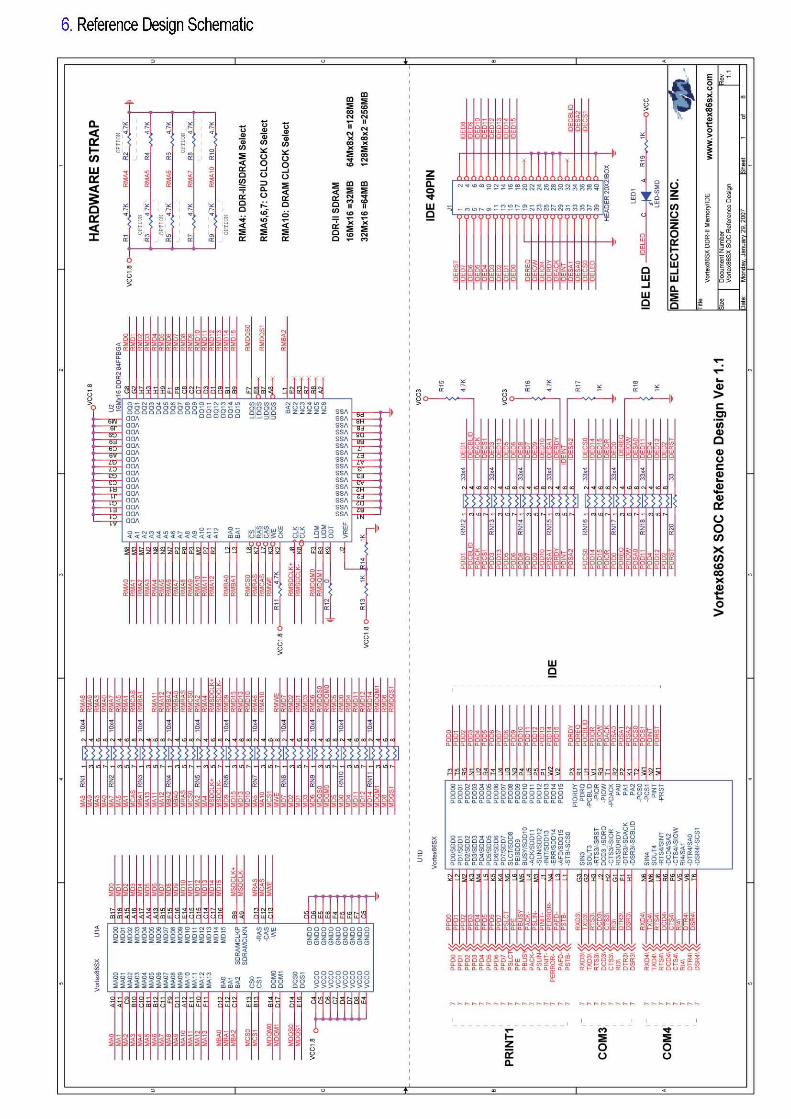
5 Rreference Design Schematic .......................................... 22
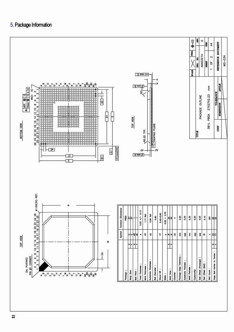
6 Package Information ........................................................ 31
Vortex86SX 32-Bit x86 Embedded SoC
Vortex86SX Brief Datasheet Version 1.000, 2/28, 2007
3
1 OverviewVortex86SX is the x86 SoC (System on Chip) with 0.13
micron process and ultra low power consumption design (less than 1 watt). This comprehensive SoC has been integrated with rich features, such as various I/O (RS-232, Parallel, USB and GPIO), BIOS, WatchDog Timer, Power Management, MTBF counter, LoC (LAN on Chip),JTAG etc., into a 27x27 mm, 581-pin BGA packing single chip. The Vortex86SX is compatible with Win CE, Linux and DOS. It integrates 32KB write through direct map L1 cache, 16-bit ISA bus, PCI Rev. 2.1 32-bit bus interface at 33 MHz, SDRAM, DDR2, ROM controller, IPC (Internal Peripheral Controllers with DMA and interrupt timer/counter included),
SPI (Serial Peripheral Interface), Fast Ethernet MAC, FIFO UART, USB2.0 Host and IDE controller into a System-on-Chip (SoC) design. Furthermore, this outstanding Vortex86SX SoC can not only meet the requirements of embedded applications, such as Electronics Billboard, Firewall Router, Industrial Single-Board-Computers, Receipt Printer Controller, Thin Client PC, Auto Vehicle Locator, Finger Print Identification, Web Camera Thin Server, RS232-to-TCP Transmitter. but also can meet the critical temperature demand, spanning from -40 to +85 ℃.
2 Features x86 Processor Core
– 6 stage pipe-line Embedded I/D Separated L1 Cache
– 16K I-Cache, 16K D-Cache SDRAM/DDRII Control Interface
– 16 bits data bus – Support DLL for clock phase auto-adjustion – SDRAM support up to 133MHz – SDRAM support up to 128Mbytes – DDRII support up to 166MHz – DDRII support up to 256Mbytes
IDE Controller – Support 2 channels Ultra-DMA 100 (Disk x 4)
LPC (Low Pin Count) Bus Interface – Support 2 programable registers to decode LPC
address MAC Controller x 1 PCI Control Interface
– Up to 3 sets PCI master device – 3.3V I/O
ISA Bus Interface – AT clock programmable – 8/16 Bit ISA device with Zero-Wait-State – Generate refresh signals to ISA interface during
DRAM refresh cycle DMA Controller Interrupt Controller
Counter/Timers
– 2 sets of 8254 timer controller – Timer output is 5V tolerance I/O on 2nd Timer
MTBF Counter Real Time Clock
– Below 2uA power comsuption on Internal Mode (Estimation Value)
FIFO UART Port x 5 (5 sets COM Port) – Compatible with 16C550/16C552 – Default internal pull-up – Supports the programmable baud rate generator
with the data rate from 50 to 460.8K bps – The character options are programmable for 1 start
bits; 1, 1.5 or 2 stop bits; even, odd or no parity; 5~8 data bits
– Support TXD_En Signal on COM1/COM2 – Port 80h output data could be sent to COM1 by
software programming Parallel Port x 1
– Support SPP/EPP/ECP mode General Chip Selector
– 2 sets extended Chip Selector – I/O-map or Memory-map could be configurable – I/O Addressing: From 2 byte to 64K byte – Memory Address: From 512 byte to 4G Byte
General Programmable I/O – Supports 40 dedicated programmable I/O pins – Each GPIO pin can be individually configured to be
an input/output pin USB 2.0 Host Support
– Supports HS, FS and LS – 4 port
PS/2 Keyboard and Mouse Interface Support – Compatible with 8042 controller
Redundant System Support Speaker out Embedded 256KB Flash
– For BIOS storage – The Flash could be disable & use external Flash
ROM JTAG Interface supported for S.W. debugging Input clock
– 14.318MHz – 32.768KHz
Output clock – 24 MHz – 25 MHz
Operating Voltage Range – Core voltage: 1.2 V ~ 1.4V – I/O voltage: 1.8V ± 5% , 3.3 V ± 10 %
Operating temperature – -40℃ ~ 85℃
Package Type – 27x27mm, 581 ball BGA
Vortex86SX 32-Bit x86 Embedded SoC
Vortex86SX Brief Datasheet
Version 1.000, 2/28 2007 4
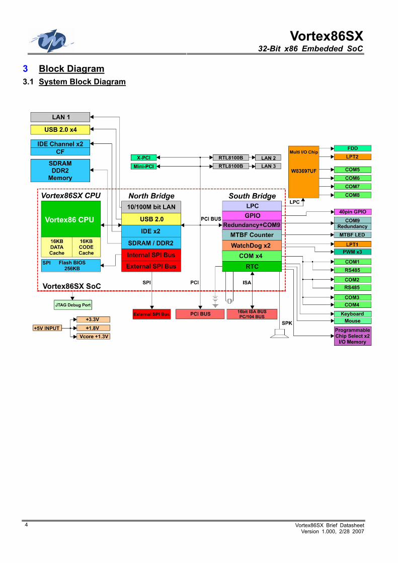
3 Block Diagram 3.1 System Block Diagram
Vortex86SX 32-Bit x86 Embedded SoC
Vortex86SX Brief Datasheet Version 1.000, 2/28, 2007
5
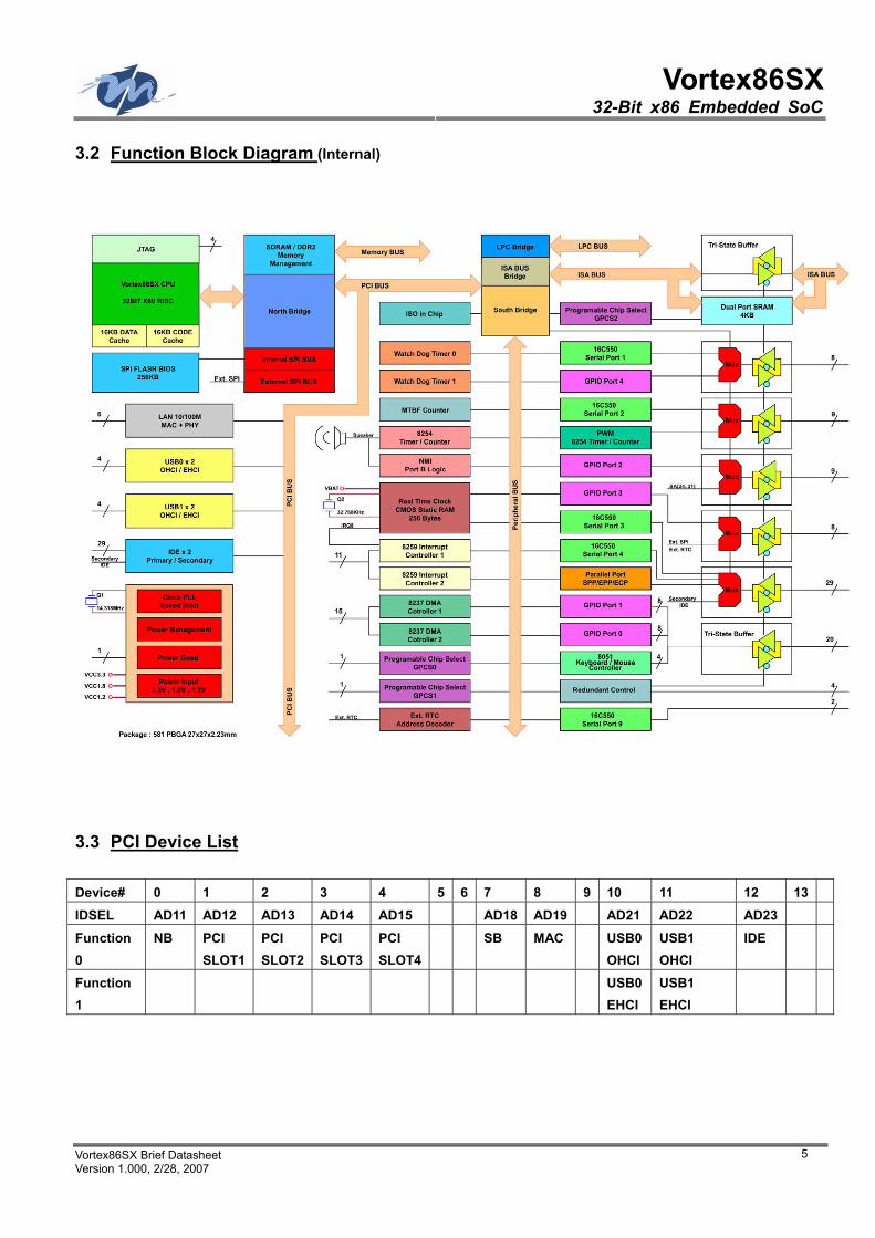
3.2 Function Block Diagram (Internal)
3.3 PCI Device List Device# 0 1 2 3 4 5 6 7 8 9 10 11 12 13IDSEL AD11 AD12 AD13 AD14 AD15 AD18 AD19 AD21 AD22 AD23 Function 0
NB PCI SLOT1
PCI SLOT2
PCI SLOT3
PCI SLOT4
SB MAC USB0 OHCI
USB1 OHCI
IDE
Function 1
USB0 EHCI
USB1 EHCI
Vortex86SX 32-Bit x86 Embedded SoC
Vortex86SX Brief Datasheet
Version 1.000, 2/28 2007 6
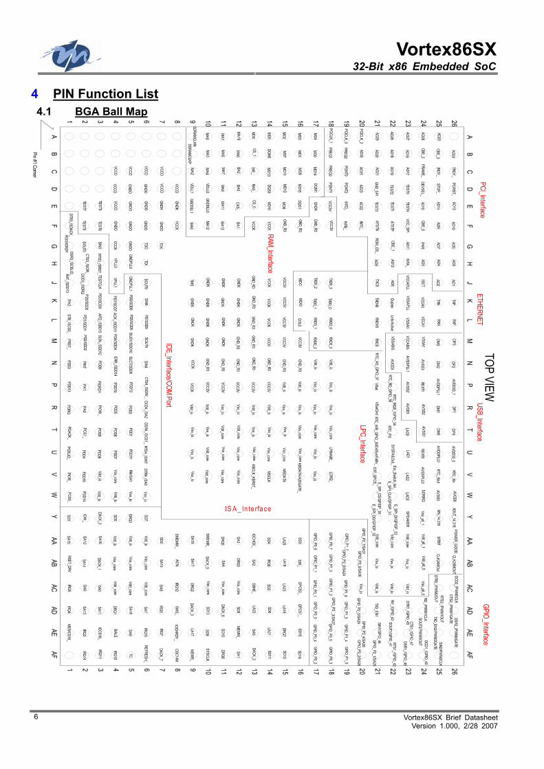
4 PIN Function List 4.1 BGA Ball Map
P
DCD4_/SA2
STB_/SCS0_
PDD0
DRQ3
TEST8
8
VCC3V
SIN1/GPIO_44
J
GNDK
Vdd_core
V
RTC_IRQ8_/GPIO_34
SD5
GPIO_P2_7/SA31
SA1
U
2
DCD2_/PWM
0CLK
VPLL0
PDD12
RXD0_3
VCC3V
AE
CBE_3
PD0/SDD0
LAD3
SD3
SA0
18
GNDK
PCI_Interface
16
REFRESH_
LA18
SA15
SA13
MA9
AB
Vss_io
Vss_io
AD9
E_SPI_DO/GPIOP_32
AD14
DCD3_/SDRQ
Vdd_core
N
PD7/SDD7
PDD2
PDRQRI3/SIORDY
DACK_7
SA18
RXD0_0
GND_R3
TRDY_
TXN
GNDK
GPIO_P1_0
GPIO_P2_5/SA29
VSSA0
IOCHCK_
AC
5
AD16
XIN_14.318
PIOW_
GNDO
Vss_io
A
AD20
SIN4
GPIO_P0_4
IOR_
IRQ9
TXEN0
GND_R3
17
SA10
OSC14M
DACK_0
0WS_
Vss_io
DSR1_/GPIO_46AD17
SIN2/PWM
2CLK
AE
M
DTR4_/SA0
PRST_
PCS1_
PDD5
SA16
Vdd_pll_1REXT1
GNDPLL0
Vss_io
CBE_2
DP0
RXD0_2
VCC3V
VBatGndRTC_W
R_GPIO_35
SD9
DRQ5
15
GNDK
6
AD5
AD25
GNDO
C
Vdd_io
Vdd_core
AF
AD24
SIN3
LAD1
KBCLK_KBRST_
SD7
ISET
TXD0_318
IRQ14
SA11
SA5
BALE
GPCS0_
GND_R3
Vss_io
AD10
STOP_
1
GNDK
DSR4_/SCS1_
BUSY/SDD10
PDD13
MA11
SD13
T
Vss_core
Vdd_io
SOUT1/GPIO_41
VCC3V
ROM_CS_
PA1
DACK_2CS_1
21
GND_R3
7
AD4
GNDO
12
GNDK
Vdd_core
Y
TDO
LAD0
VSSA1
SA19
IRQ3
Vdd_core
19
IRQ10
SA6
CTS4_/SIOW_
MD13
PGNT0
CAS_
VCCO
TEST3
VCC3V
Vss_io
AD6RTC_PS
EXT_GPCS_
DSR3_/SCBLID_
PE/SDD9
MA8
DACK_3
Y
Vss_core
GND_R3
Vdd_io
GNDO
Vss_core
L
RTC_AS_GPIO_37
MA2
ACK_/SDD11VPLL1
DQM0
MDIO
VCCK
8
AD3
VCCO
VCCAPLL
RXP
Vss_core
AD21
AD27
Vss_pll_1
PREQ0
INTA_
MSCLK
L
IRQ6
PA0
SDRAMCLKP
GPIO_P1_5
BA0
MD2
Vss_io
Vss_core
AD11
CLK24MOut
TXD0_2
PDD8PDD9
DQM1
17
GND_R3
AF
Vdd_io
K
PCIRST_
MA10
PCS0_
GNDPLL1
DRQ6
Vdd_io
9
AD2
DTR1_/GPIO_45
IRDY_DM
0
10
Vss_core
AD28
PREQ1
POWER_GOOD
DRQ2
3
GNDK
LA22
MD12
GPIO_P1_4
IOCHRDY_
MD7
R
Vdd_core
VCC3V
Vss_io
Vss_io
TOP VIEW
E_SPI_DI/GPIOP_33
AD15
AVDD33_0
TEST1
SD12
PDD6
PDD15
DQS1
25
VCCO
9
GND_R3
H
J
22
VBatAD29
SA7
DRQ0
SD14
P
Vss_core
10
AD1
RTS2_/PWM
1OUT
SOUT2/PWM
0OUT
RXN
AVSSPLL0
MDC
VCC3V
Vss_core
GPIO_P2_4/SA28
SOUT9
PREQ2
GPIO_P2_1/SA25
AVDD1
19
GNDK
AA
MD1
MA4
GPIO_P1_1
GPCS1_
PDD11
W Vss_io
Vss_ioVss_io
RTC_Xin
PIOR_
INTB_
Vdd_core
IRQ11
PDD7
DRQ7
SDRAMCLKN
GND_R3
R
VCC3V
VCC3V
H
23CTS1_/GPIO_47
MA3
SA2
LA23
AD0
CTS2_/PWM
1GATE
RTC_Xout
VSSAPLL
Vss_io
Vss_core
GNDO
RAM_Interface
TCK
RTS4_/SINT
GPIO_P0_5
VCCA0
AVDD3
AVSS1
TEST0
VCCK
SA8
PD3/SDD3
PCICLK_0
GPIO_P2_3/SA27
PDD3
Vss_io
Vss_io
AD18
SMEM
R_
SBHE_
MD9
SA9
LA17
VCCO
VCCO
AD7
COL0
G
ExtSysFailIn_
TC
MD15
GND_SPI
SA14
16
CLK25MOUT
DSR2_/PWM
0GATE
DTR2_/PWM
2OUT
TXP
N
Vss_core
GNDO
IDE_Interface/COM Port
T
11
SYSFAILOut_
FRAME_
PIORDY
Vdd_pll_0VCCA1
AVDDPLL1
AVSS3
AVDDPLL0
GNDO
INIT_/SDD13
PCICLK_1
GPIO_P1_6
MD5
24
GND_R3
Vss_io
AD19
AVDD33_1
2
GNDK
PDD14
DACK_1
VCCO
G
Vdd_core
RI1_/GPIO_43
PD1/SDD1
Vss_pll_0
RXD0_1
VCC3V
F
TMS
XOUT_14.318
LA20
RTS3_/SRST_
MA6
VDLL0
SD10
20
GND_R3
Pin #1 Corner
TXD_EN2/PWM
2GATE
VCCABG
GNDK
Vss_core
VCCK
IS A _ In te rfa ce
W
AD30
PINT
SERIRQ
GNDDLL0
Vss_core
IRQ15
MA5
TXD0_1
VCCK
Vss_io
RI2_/PWM
1CLK
KBDATA/A20GATE_
6
GNDK
TESTCLK
PD5/SDD5
IRQ12VCCO
K
VCCK
Vdd_io
AD12
SOUT4
Vdd_core
E
SPEAKER
TDI
LA21M
D10
RI4/SA1
SD8
VCC_SPI
RXC0
VCCK
3
E_SPI_CS/GPIOP_30
REXT0
SD4
GNDK
Vss_core
VCCK
GPIO_Interface
AD26
SIN9
GPIO_P0_6
GNDDLL1
A
20
MA7
PDD4
Vss_io
Vss_io
12
LFRAME_
SA17
SD2
TEST2
UAB
SYSCLK
DRQ1
GPIO_P1_2
INTD_
Vdd_io
DP3
AFD_/SDD15
M
Vdd_io
D
1
Ext_Switch_fail_
SLCT/SDD8
CTS3_/SIOR_
SD1
DQS0
AVDD0
GNDO
Vdd_ioE_SPI_CLK/GPIOP_31
DEVSEL_
DACK_5
TEST5
22
Vss_coreGND_R3
LPC_InterfaceGPIO_P2_6/SA30
MD14
PGNT1
SD6
5
GNDK
21
MD6
SD15
GNDO
D
Vdd_io
Vss_io13
GPIO_P0_1
SMEM
W_
AVSSPLL1
IRQ5
MA12
GPIO_P1_3
INTC_
Link/Active
23
GND_R3Vdd_io
TXD_EN1
MTBF
MD4
26
GNDK
C
PDD1
PA2
MD8
CS_0
F
Vss_core
AD
DM3
CBE_1
AD22
RSET_DRV
TXD0_0
VCC3V
GND_R3
RTC_RD_GPIO_36
MEM
CS16_
SOUT3
GPIO_P0_2
AVSS0
7
GND_R3
USB_Interface
244
SD0
VCCO
V
GNDK
14
LAD2
AVDD2
VDLL1
Vss_core
IRQ7
PD6/SDD6
MA13
PCICLK_2
GPIO_P1_7
RXDV0
VCCKVdd_io
AD8
VSSABG
ERR_/SDD144
GNDK
B
MD11
SLIN_/SDD12
DTR3_/SDACK_
WE_
TEST7
AA
DM2
AD13
AD23
SA12
VCC3V
VCCK
ATSTP
AD31
MA0
PDD10
GPIO_P0_7
MEM
W_
11
VCCK
ETHERNET
26
SA4
Vss_core
15
PGNT2
MSDATA
AD IRQ4
LA19
PD4/SDD4
MEM
R_
GPIO_P2_2/SA26
GPIO_P2_0/SA24
Vdd_io
Vdd_io
Vss_io
DP2
DCD1_/GPIO_40
MD3
TEST4
PD2/SDD2
PCBLID_
IOW_
DACK_6
TEST6
13
DM1
PAR
RTS1_/GPIO_42
B
Vdd_io
Vdd_core
AC
ATSTN
MA1
PDACK_
LDRQ_
Duplex
GND_R3
SA3
25
Vss_core
GPIO_P0_3
GPIO_P0_0
AEN
AVSS2
14
GNDK
RAS_
BA2
SD11
IOCS16_
BA1
E
Vdd_io
Vdd_io
Vss_io
CBE_0
DP1
MD0
TXC0
Vortex86SX 32-Bit x86 Embedded SoC
Vortex86SX Brief Datasheet Version 1.000, 2/28, 2007
7
4.2 Signal Description This chapter provides a detailed description of Vortex86SX signals. A signal with the symbol ”_n” at the end of itself indicates
that this pin is low active. Otherwise, it is high active.
The following notations are used to describe the signal types:
I Input pin
O Output pin OD Output pin with open-drain I/O Bi-directional Input/Output pin
System (7 PINs)
PIN No. Symbol Type Description
AA26 PWRGOOD I Power-Good Input. This signal comes from Power Good of the power supply to indicate that the power is available. The Vortex86SX uses this signal to generate reset sequence for the system.
AB26 25MOUT O 25MHz Clock output. Y26 XOUT_14.318 O Crystal-out. Frequency output from the inverting amplifier (oscillator).
Y25 XIN_14.318 I Crystal-in. 14.318MHz frequency input, within 100 ppm tolerance, to the amplifier (oscillator).
AA25 MTBF MTBF Flag output. AB25 CLK24MOUT O 24MHz Clock output
Y23 SPEAKER O Speaker Output. This pin is used to control the Speaker Output and should be connected to the Speaker
SDRAM /DDRII Interface (44 PINs)
PIN No. Symbol Type Description
B9 SDRAMCLK O Clock output. This pin provides the fundamental timing for the SDRAM /DDR controller.
A9 SDRAMCLKN O Clock output. This pin provides the fundamental timing for the SDRAM /DDR controller.
D13 RAS_ O Row Address Strobe. When asserted, this signal latches row address on positive edge of the SDRAM/DDR clock. This signal also allows row access and pre-charge.
E12 CAS_ O Column Address Strobe. When asserted, this signal latches column address on the positive edge of the SDRAM/DDR clock. This signal also allows column access and pre-charge.
C13 WE_ O Memory Write Enable. This pin is used as a write enable for the memory data bus.
B13, E13 CS_[1:0] O
Chip Select CS[1:0]. These two pins activate the SDRAM devices. First Bank of SDRAM accepts any command when the CS0_n pin is active low. Second Bank of SDRAM accepts any command when the CS1_n pin is active low. For DDRII, only CS0_n activates the DDR device.
B14, D17 DQM[1:0] O Data Mask DQM[1:0]. These pins act as synchronized output enables during read cycles and byte masks during write cycles.
E16, D14 DQS[1:0] I/O Data Strobe DQS[1:0 for DDR only. Output with write data, input with the read data for source synchronous operation.
Vortex86SX 32-Bit x86 Embedded SoC
Vortex86SX Brief Datasheet
Version 1.000, 2/28 2007 8
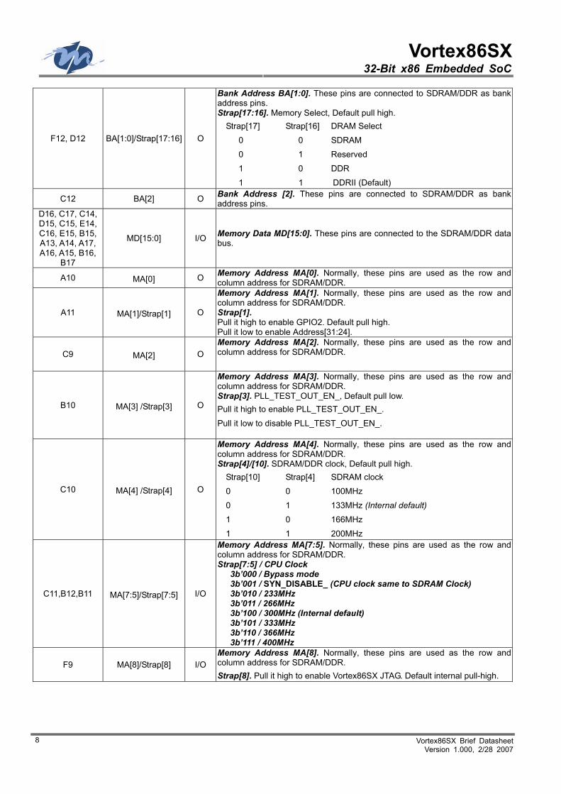
F12, D12 BA[1:0]/Strap[17:16] O
Bank Address BA[1:0]. These pins are connected to SDRAM/DDR as bank address pins. Strap[17:16]. Memory Select, Default pull high.
Strap[17] Strap[16] DRAM Select
0 0 SDRAM
0 1 Reserved
1 0 DDR
1 1 DDRII (Default)
C12 BA[2] O Bank Address [2]. These pins are connected to SDRAM/DDR as bank address pins.
D16, C17, C14, D15, C15, E14, C16, E15, B15, A13, A14, A17, A16, A15, B16,
B17
MD[15:0] I/O Memory Data MD[15:0]. These pins are connected to the SDRAM/DDR data bus.
A10 MA[0] O Memory Address MA[0]. Normally, these pins are used as the row and column address for SDRAM/DDR.
A11 MA[1]/Strap[1] O
Memory Address MA[1]. Normally, these pins are used as the row and column address for SDRAM/DDR. Strap[1]. Pull it high to enable GPIO2. Default pull high. Pull it low to enable Address[31:24].
C9 MA[2] O Memory Address MA[2]. Normally, these pins are used as the row and column address for SDRAM/DDR.
B10 MA[3] /Strap[3] O
Memory Address MA[3]. Normally, these pins are used as the row and column address for SDRAM/DDR. Strap[3]. PLL_TEST_OUT_EN_, Default pull low. Pull it high to enable PLL_TEST_OUT_EN_.
Pull it low to disable PLL_TEST_OUT_EN_.
C10 MA[4] /Strap[4] O
Memory Address MA[4]. Normally, these pins are used as the row and column address for SDRAM/DDR. Strap[4]/[10]. SDRAM/DDR clock, Default pull high.
Strap[10] Strap[4] SDRAM clock
0 0 100MHz
0 1 133MHz (Internal default)
1 0 166MHz
1 1 200MHz
C11,B12,B11 MA[7:5]/Strap[7:5] I/O
Memory Address MA[7:5]. Normally, these pins are used as the row and column address for SDRAM/DDR. Strap[7:5] / CPU Clock
3b’000 / Bypass mode 3b’001 / SYN_DISABLE_ (CPU clock same to SDRAM Clock) 3b’010 / 233MHz 3b’011 / 266MHz 3b’100 / 300MHz (Internal default) 3b’101 / 333MHz 3b’110 / 366MHz 3b’111 / 400MHz
F9 MA[8]/Strap[8] I/O Memory Address MA[8]. Normally, these pins are used as the row and column address for SDRAM/DDR. Strap[8]. Pull it high to enable Vortex86SX JTAG. Default internal pull-high.
Vortex86SX 32-Bit x86 Embedded SoC
Vortex86SX Brief Datasheet Version 1.000, 2/28, 2007
9
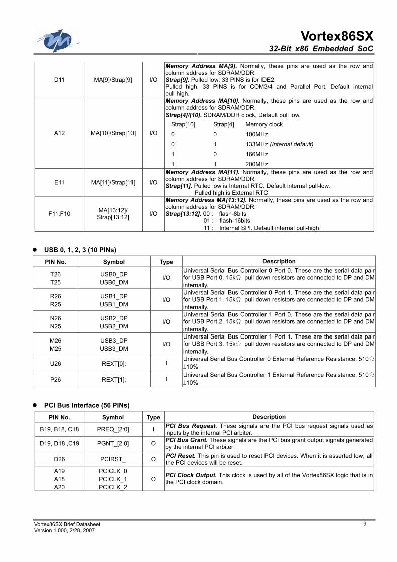
D11 MA[9]/Strap[9] I/O
Memory Address MA[9]. Normally, these pins are used as the row and column address for SDRAM/DDR. Strap[9]. Pulled low: 33 PINS is for IDE2. Pulled high: 33 PINS is for COM3/4 and Parallel Port. Default internal pull-high.
A12 MA[10]/Strap[10] I/O
Memory Address MA[10]. Normally, these pins are used as the row and column address for SDRAM/DDR. Strap[4]/[10]. SDRAM/DDR clock, Default pull low.
Strap[10] Strap[4] Memory clock
0 0 100MHz
0 1 133MHz (Internal default)
1 0 166MHz
1 1 200MHz
E11 MA[11]/Strap[11] I/O
Memory Address MA[11]. Normally, these pins are used as the row and column address for SDRAM/DDR. Strap[11]. Pulled low is Internal RTC. Default internal pull-low.
Pulled high is External RTC
F11,F10 MA[13:12]/ Strap[13:12] I/O
Memory Address MA[13:12]. Normally, these pins are used as the row and column address for SDRAM/DDR. Strap[13:12]. 00 : flash-8bits
01 : flash-16bits 11 : Internal SPI. Default internal pull-high.
USB 0, 1, 2, 3 (10 PINs)
PIN No. Symbol Type Description
T26 T25
USB0_DP USB0_DM
I/O Universal Serial Bus Controller 0 Port 0. These are the serial data pair for USB Port 0. 15kΩ pull down resistors are connected to DP and DM internally.
R26 R25
USB1_DP USB1_DM
I/O Universal Serial Bus Controller 0 Port 1. These are the serial data pair for USB Port 1. 15kΩ pull down resistors are connected to DP and DM internally.
N26 N25
USB2_DP USB2_DM
I/O Universal Serial Bus Controller 1 Port 0. These are the serial data pair for USB Port 2. 15kΩ pull down resistors are connected to DP and DM internally.
M26 M25
USB3_DP USB3_DM
I/O Universal Serial Bus Controller 1 Port 1. These are the serial data pair for USB Port 3. 15kΩ pull down resistors are connected to DP and DM internally.
U26 REXT[0]: I Universal Serial Bus Controller 0 External Reference Resistance. 510Ω±10%
P26 REXT[1]: I Universal Serial Bus Controller 1 External Reference Resistance. 510Ω±10%
PCI Bus Interface (56 PINs)
PIN No. Symbol Type Description
B19, B18, C18 PREQ_[2:0] I PCI Bus Request. These signals are the PCI bus request signals used as inputs by the internal PCI arbiter.
D19, D18 ,C19 PGNT_[2:0] O PCI Bus Grant. These signals are the PCI bus grant output signals generated by the internal PCI arbiter.
D26 PCIRST_ O PCI Reset. This pin is used to reset PCI devices. When it is asserted low, all the PCI devices will be reset.
A19 A18 A20
PCICLK_0 PCICLK_1 PCICLK_2
O PCI Clock Output. This clock is used by all of the Vortex86SX logic that is in the PCI clock domain.
Vortex86SX 32-Bit x86 Embedded SoC
Vortex86SX Brief Datasheet
Version 1.000, 2/28 2007 10
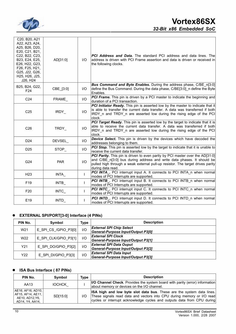
C20, B20, A21 A22, A23, A24, A25, B26, D20, E20, C21, B21, C22, B22, C23, B23, E24, E25, E26, H22, G23, F26, F25, H21, G25, J22, G26, H25, H26, J25,
J26, H24
AD[31:0] I/O PCI Address and Data. The standard PCI address and data lines. The address is driven with PCI Frame assertion and data is driven or received in the following clocks.
B25, B24, G22, F24 CBE_[3:0] I/O
Bus Command and Byte Enables. During the address phase, C/BE_n[3:0] define the Bus Command. During the data phase, C/BE[3:0]_n define the Byte Enables.
C24 FRAME_ I/O PCI Frame. This pin is driven by a PCI master to indicate the beginning and duration of a PCI transaction.
C25 IRDY_ I/O
PCI Initiator Ready. This pin is asserted low by the master to indicate that it is able to transfer the current data transfer. A data was transferred if both IRDY_n and TRDY_n are asserted low during the rising edge of the PCI clock.
C26 TRDY_ I/O
PCI Target Ready. This pin is asserted low by the target to indicate that it is able to receive the current data transfer. A data was transferred if both IRDY_n and TRDY_n are asserted low during the rising edge of the PCI clock.
D24 DEVSEL_ I/O Device Select. This pin is driven by the devices which have decoded the addresses belonging to them.
D25 STOP_ I/O PCI Stop. This pin is asserted low by the target to indicate that it is unable to receive the current data transfer.
G24 PAR I/O
PCI Parity. This pin is driven to even parity by PCI master over the AD[31:0] and C/BE_n[3:0] bus during address and write data phases. It should be pulled high through a weak external pull-up resistor. The target drives parity during data read.
H23 INTA_ I PCI INTA_. PCI interrupt input A. It connects to PCI INTA_n when normal modes of PCI Interrupts are supported.
F19 INTB_ I PCI INTB_. PCI interrupt input B. It connects to PCI INTB_n when normal modes of PCI Interrupts are supported.
F20 INTC_ I PCI INTC_. PCI interrupt input C. It connects to PCI INTC_n when normal modes of PCI Interrupts are supported.
E19 INTD_ I PCI INTD_. PCI interrupt input D. It connects to PCI INTD_n when normal modes of PCI Interrupts are supported.
EXTERNAL SPI/PORT[3-0] Interface (4 PINs)
PIN No. Symbol Type Description
W21 E_SPI_CS_/GPIO_P3[0] I/O External SPI Chip Select General-Purpose Input/Output P3[0]
W22 E_SPI_CLK/GPIO_P3[1] I/O External SPI Clock General-Purpose Input/Output P3[1]
Y21 E_SPI_DO/GPIO_P3[2] I/O External SPI Data Ouput General-Purpose Input/Output P3[2]
Y22 E_SPI_DI/GPIO_P3[3] I/O External SPI Data Input General-Purpose Input/Output P3[3]
ISA Bus Interface ( 87 PINs)
PIN No. Symbol Type Description
AA13 IOCHCK_ I I/O Channel Check. Provides the system board with parity (error) information about memory or devices on the I/O channel.
AE16, AF16, AD10, AF15, AF14, AE11,
AE10, AD12,Y6, AD14, Y4, AA14,
SD[15:0] I/O ISA high and low byte slot data bus. These are the system data lines.These signals read data and vectors into CPU during memory or I/O readcycles or interrupt acknowledge cycles and outputs data from CPU during
Vortex86SX 32-Bit x86 Embedded SoC
Vortex86SX Brief Datasheet Version 1.000, 2/28, 2007
11
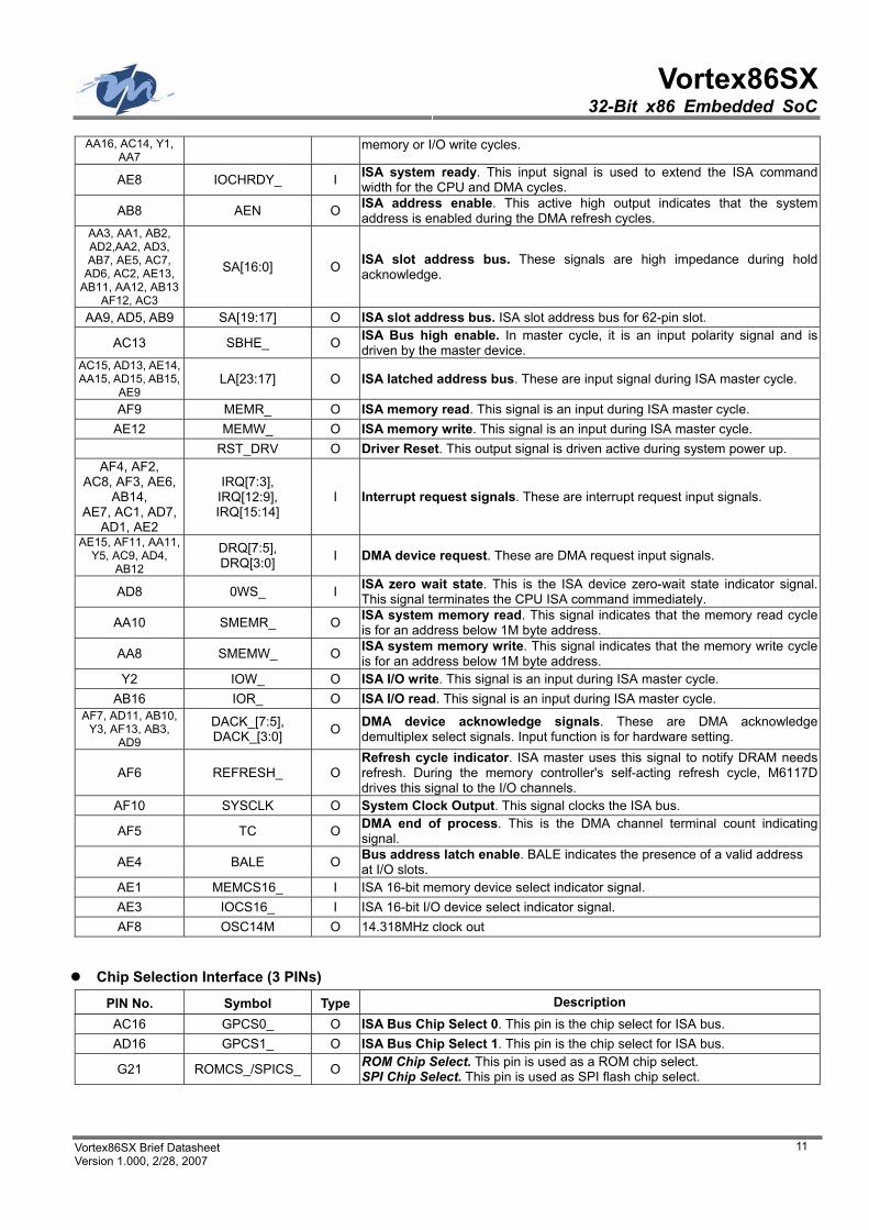
AA16, AC14, Y1, AA7
memory or I/O write cycles.
AE8 IOCHRDY_ I ISA system ready. This input signal is used to extend the ISA commandwidth for the CPU and DMA cycles.
AB8 AEN O ISA address enable. This active high output indicates that the systemaddress is enabled during the DMA refresh cycles.
AA3, AA1, AB2, AD2,AA2, AD3, AB7, AE5, AC7,
AD6, AC2, AE13, AB11, AA12, AB13
AF12, AC3
SA[16:0] O ISA slot address bus. These signals are high impedance during holdacknowledge.
AA9, AD5, AB9 SA[19:17] O ISA slot address bus. ISA slot address bus for 62-pin slot.
AC13 SBHE_ O ISA Bus high enable. In master cycle, it is an input polarity signal and isdriven by the master device.
AC15, AD13, AE14, AA15, AD15, AB15,
AE9 LA[23:17] O ISA latched address bus. These are input signal during ISA master cycle.
AF9 MEMR_ O ISA memory read. This signal is an input during ISA master cycle. AE12 MEMW_ O ISA memory write. This signal is an input during ISA master cycle.
RST_DRV O Driver Reset. This output signal is driven active during system power up. AF4, AF2,
AC8, AF3, AE6, AB14,
AE7, AC1, AD7, AD1, AE2
IRQ[7:3], IRQ[12:9], IRQ[15:14]
I Interrupt request signals. These are interrupt request input signals.
AE15, AF11, AA11, Y5, AC9, AD4,
AB12
DRQ[7:5], DRQ[3:0] I DMA device request. These are DMA request input signals.
AD8 0WS_ I ISA zero wait state. This is the ISA device zero-wait state indicator signal.This signal terminates the CPU ISA command immediately.
AA10 SMEMR_ O ISA system memory read. This signal indicates that the memory read cycleis for an address below 1M byte address.
AA8 SMEMW_ O ISA system memory write. This signal indicates that the memory write cycleis for an address below 1M byte address.
Y2 IOW_ O ISA I/O write. This signal is an input during ISA master cycle. AB16 IOR_ O ISA I/O read. This signal is an input during ISA master cycle.
AF7, AD11, AB10, Y3, AF13, AB3,
AD9
DACK_[7:5], DACK_[3:0] O DMA device acknowledge signals. These are DMA acknowledge
demultiplex select signals. Input function is for hardware setting.
AF6 REFRESH_ O Refresh cycle indicator. ISA master uses this signal to notify DRAM needsrefresh. During the memory controller's self-acting refresh cycle, M6117Ddrives this signal to the I/O channels.
AF10 SYSCLK O System Clock Output. This signal clocks the ISA bus.
AF5 TC O DMA end of process. This is the DMA channel terminal count indicatingsignal.
AE4 BALE O Bus address latch enable. BALE indicates the presence of a valid address at I/O slots.
AE1 MEMCS16_ I ISA 16-bit memory device select indicator signal. AE3 IOCS16_ I ISA 16-bit I/O device select indicator signal. AF8 OSC14M O 14.318MHz clock out
Chip Selection Interface (3 PINs)
PIN No. Symbol Type Description AC16 GPCS0_ O ISA Bus Chip Select 0. This pin is the chip select for ISA bus. AD16 GPCS1_ O ISA Bus Chip Select 1. This pin is the chip select for ISA bus.
G21 ROMCS_/SPICS_ O ROM Chip Select. This pin is used as a ROM chip select. SPI Chip Select. This pin is used as SPI flash chip select.
Vortex86SX 32-Bit x86 Embedded SoC
Vortex86SX Brief Datasheet
Version 1.000, 2/28 2007 12
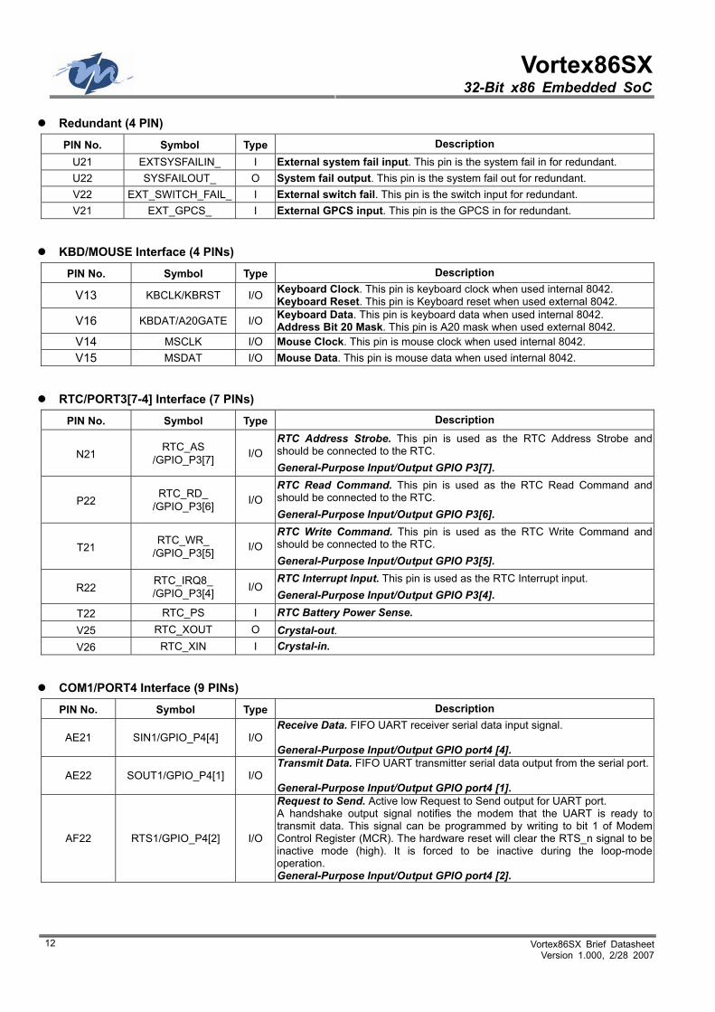
Redundant (4 PIN)
PIN No. Symbol Type Description U21 EXTSYSFAILIN_ I External system fail input. This pin is the system fail in for redundant. U22 SYSFAILOUT_ O System fail output. This pin is the system fail out for redundant. V22 EXT_SWITCH_FAIL_ I External switch fail. This pin is the switch input for redundant. V21 EXT_GPCS_ I External GPCS input. This pin is the GPCS in for redundant.
KBD/MOUSE Interface (4 PINs)
PIN No. Symbol Type Description
V13 KBCLK/KBRST I/O Keyboard Clock. This pin is keyboard clock when used internal 8042. Keyboard Reset. This pin is Keyboard reset when used external 8042.
V16 KBDAT/A20GATE I/O Keyboard Data. This pin is keyboard data when used internal 8042. Address Bit 20 Mask. This pin is A20 mask when used external 8042.
V14 MSCLK I/O Mouse Clock. This pin is mouse clock when used internal 8042. V15 MSDAT I/O Mouse Data. This pin is mouse data when used internal 8042.
RTC/PORT3[7-4] Interface (7 PINs)
PIN No. Symbol Type Description
N21 RTC_AS
/GPIO_P3[7] I/O RTC Address Strobe. This pin is used as the RTC Address Strobe and should be connected to the RTC. General-Purpose Input/Output GPIO P3[7].
P22 RTC_RD_
/GPIO_P3[6] I/O RTC Read Command. This pin is used as the RTC Read Command and should be connected to the RTC. General-Purpose Input/Output GPIO P3[6].
T21 RTC_WR_
/GPIO_P3[5] I/O RTC Write Command. This pin is used as the RTC Write Command and should be connected to the RTC. General-Purpose Input/Output GPIO P3[5].
R22 RTC_IRQ8_ /GPIO_P3[4] I/O
RTC Interrupt Input. This pin is used as the RTC Interrupt input. General-Purpose Input/Output GPIO P3[4].
T22 RTC_PS I RTC Battery Power Sense. V25 RTC_XOUT O Crystal-out. V26 RTC_XIN I Crystal-in.
COM1/PORT4 Interface (9 PINs)
PIN No. Symbol Type Description
AE21 SIN1/GPIO_P4[4] I/O Receive Data. FIFO UART receiver serial data input signal. General-Purpose Input/Output GPIO port4 [4].
AE22 SOUT1/GPIO_P4[1] I/O Transmit Data. FIFO UART transmitter serial data output from the serial port. General-Purpose Input/Output GPIO port4 [1].
AF22 RTS1/GPIO_P4[2] I/O
Request to Send. Active low Request to Send output for UART port. A handshake output signal notifies the modem that the UART is ready to transmit data. This signal can be programmed by writing to bit 1 of Modem Control Register (MCR). The hardware reset will clear the RTS_n signal to be inactive mode (high). It is forced to be inactive during the loop-mode operation. General-Purpose Input/Output GPIO port4 [2].
Vortex86SX 32-Bit x86 Embedded SoC
Vortex86SX Brief Datasheet Version 1.000, 2/28, 2007
13
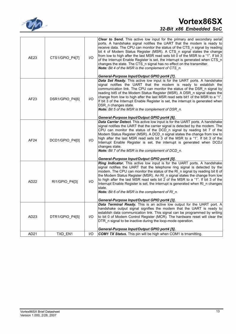
AE23 CTS1/GPIO_P4[7] I/O
Clear to Send. This active low input for the primary and secondary serial ports. A handshake signal notifies the UART that the modem is ready to receive data. The CPU can monitor the status of the CTS_n signal by reading bit 4 of Modem Status Register (MSR). A CTS_n signal states the change from low to high after the last MSR read sets bit 0 of the MSR to a “1”. If bit 3 of the Interrupt Enable Register is set, the interrupt is generated when CTS_n changes the state. The CTS_n signal has no effect on the transmitter. Note: Bit 4 of the MSR is the complement of CTS_n. General-Purpose Input/Output GPIO port4 [7].
AF23 DSR1/GPIO_P4[6] I/O
Data Set Ready. This active low input is for the UART ports. A handshake signal notifies the UART that the modem is ready to establish the communication link. The CPU can monitor the status of the DSR_n signal by reading bit5 of the Modem Status Register (MSR). A DSR_n signal states the change from low to high after the last MSR read sets bit1 of the MSR to a “1”. If bit 3 of the Interrupt Enable Register is set, the interrupt is generated when DSR_n changes state. Note: Bit 5 of the MSR is the complement of DSR_n. General-Purpose Input/Output GPIO port4 [6].
AF24 DCD1/GPIO_P4[0] I/O
Data Carrier Detect. This active low input is for the UART ports. A handshake signal notifies the UART that the carrier signal is detected by the modem. The CPU can monitor the status of the DCD_n signal by reading bit 7 of the Modem Status Register (MSR). A DCD_n signal states the change from low to high after the last MSR read sets bit 3 of the MSR to a “1”. If bit 3 of the Interrupt Enable Register is set, the interrupt is generated when DCDJ changes state. Note: Bit 7 of the MSR is the complement of DCD_n. General-Purpose Input/Output GPIO port4 [0].
AD22 RI1/GPIO_P4[3] I/O
Ring Indicator. This active low input is for the UART ports. A handshake signal notifies the UART that the telephone ring signal is detected by the modem. The CPU can monitor the status of the RI_n signal by reading bit 6 of the Modem Status Register (MSR). An RI_n signal states the change from low to high after the last MSR read sets bit 2 of the MSR to a “1”. If bit 3 of the Interrupt Enable Register is set, the interrupt is generated when RI_n changes state. Note: Bit 6 of the MSR is the complement of RI_n. General-Purpose Input/Output GPIO port4 [3].
AD23 DTR1/GPIO_P4[5] I/O
Data Terminal Ready. This is an active low output for the UART port. A handshake output signal signifies the modem that the UART is ready to establish data communication link. This signal can be programmed by writing to bit 0 of Modem Control Register (MCR). The hardware reset will clear the DTR_n signal to be inactive during the loop-mode operation. General-Purpose Input/Output GPIO port4 [5].
AD21 TXD_EN1 I/O COM1 TX Status. This pin will be high when COM1 is trnamitting.
Vortex86SX 32-Bit x86 Embedded SoC
Vortex86SX Brief Datasheet
Version 1.000, 2/28 2007 14
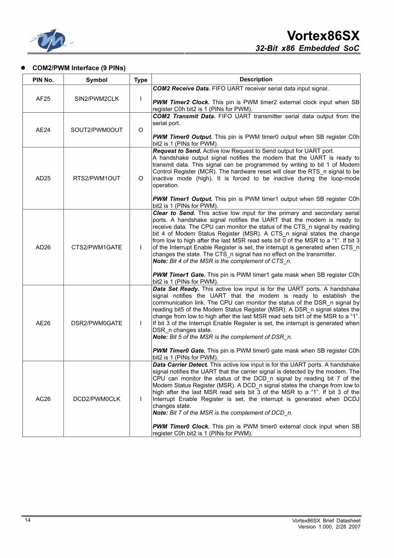
COM2/PWM Interface (9 PINs)
PIN No. Symbol Type Description
AF25 SIN2/PWM2CLK I
COM2 Receive Data. FIFO UART receiver serial data input signal. PWM Timer2 Clock. This pin is PWM timer2 external clock input when SB register C0h bit2 is 1 (PINs for PWM).
AE24 SOUT2/PWM0OUT O
COM2 Transmit Data. FIFO UART transmitter serial data output from the serial port. PWM Timer0 Output. This pin is PWM timer0 output when SB register C0h bit2 is 1 (PINs for PWM).
AD25 RTS2/PWM1OUT O
Request to Send. Active low Request to Send output for UART port. A handshake output signal notifies the modem that the UART is ready to transmit data. This signal can be programmed by writing to bit 1 of Modem Control Register (MCR). The hardware reset will clear the RTS_n signal to be inactive mode (high). It is forced to be inactive during the loop-mode operation. PWM Timer1 Output. This pin is PWM timer1 output when SB register C0h bit2 is 1 (PINs for PWM).
AD26 CTS2/PWM1GATE I
Clear to Send. This active low input for the primary and secondary serial ports. A handshake signal notifies the UART that the modem is ready to receive data. The CPU can monitor the status of the CTS_n signal by reading bit 4 of Modem Status Register (MSR). A CTS_n signal states the change from low to high after the last MSR read sets bit 0 of the MSR to a “1”. If bit 3 of the Interrupt Enable Register is set, the interrupt is generated when CTS_n changes the state. The CTS_n signal has no effect on the transmitter. Note: Bit 4 of the MSR is the complement of CTS_n. PWM Timer1 Gate. This pin is PWM timer1 gate mask when SB register C0h bit2 is 1 (PINs for PWM).
AE26 DSR2/PWM0GATE I
Data Set Ready. This active low input is for the UART ports. A handshake signal notifies the UART that the modem is ready to establish the communication link. The CPU can monitor the status of the DSR_n signal by reading bit5 of the Modem Status Register (MSR). A DSR_n signal states the change from low to high after the last MSR read sets bit1 of the MSR to a “1”. If bit 3 of the Interrupt Enable Register is set, the interrupt is generated when DSR_n changes state. Note: Bit 5 of the MSR is the complement of DSR_n. PWM Timer0 Gate. This pin is PWM timer0 gate mask when SB register C0h bit2 is 1 (PINs for PWM).
AC26 DCD2/PWM0CLK I
Data Carrier Detect. This active low input is for the UART ports. A handshake signal notifies the UART that the carrier signal is detected by the modem. The CPU can monitor the status of the DCD_n signal by reading bit 7 of the Modem Status Register (MSR). A DCD_n signal states the change from low to high after the last MSR read sets bit 3 of the MSR to a “1”. If bit 3 of the Interrupt Enable Register is set, the interrupt is generated when DCDJ changes state. Note: Bit 7 of the MSR is the complement of DCD_n. PWM Timer0 Clock. This pin is PWM timer0 external clock input when SB register C0h bit2 is 1 (PINs for PWM).
Vortex86SX 32-Bit x86 Embedded SoC
Vortex86SX Brief Datasheet Version 1.000, 2/28, 2007
15
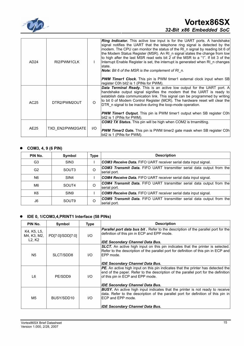
AD24 RI2/PWM1CLK I
Ring Indicator. This active low input is for the UART ports. A handshake signal notifies the UART that the telephone ring signal is detected by the modem. The CPU can monitor the status of the RI_n signal by reading bit 6 of the Modem Status Register (MSR). An RI_n signal states the change from low to high after the last MSR read sets bit 2 of the MSR to a “1”. If bit 3 of the Interrupt Enable Register is set, the interrupt is generated when RI_n changes state. Note: Bit 6 of the MSR is the complement of RI_n. PWM Timer1 Clock. This pin is PWM timer1 external clock input when SB register C0h bit2 is 1 (PINs for PWM).
AC25 DTR2/PWM2OUT O
Data Terminal Ready. This is an active low output for the UART port. A handshake output signal signifies the modem that the UART is ready to establish data communication link. This signal can be programmed by writing to bit 0 of Modem Control Register (MCR). The hardware reset will clear the DTR_n signal to be inactive during the loop-mode operation. PWM Timer1 Output. This pin is PWM timer1 output when SB register C0h bit2 is 1 (PINs for PWM).
AE25 TXD_EN2/PWM2GATE I/O
COM2 TX Status. This pin will be high when COM2 is trnamitting. PWM Timer2 Gate. This pin is PWM timer2 gate mask when SB register C0h bit2 is 1 (PINs for PWM).
COM3, 4, 9 (6 PIN)
PIN No. Symbol Type Description
G3 SIN3 I COM3 Receive Data. FIFO UART receiver serial data input signal.
G2 SOUT3 O COM3 Transmit Data. FIFO UART transmitter serial data output from the serial port.
N6 SIN4 I COM4 Receive Data. FIFO UART receiver serial data input signal.
M6 SOUT4 O COM4 Transmit Data. FIFO UART transmitter serial data output from the serial port.
K6 SIN9 I COM9 Receive Data. FIFO UART receiver serial data input signal.
J6 SOUT9 O COM9 Transmit Data. FIFO UART transmitter serial data output from the serial port.
IDE 0, 1/COM3,4,PRINT1 Interface (58 PINs)
PIN No. Symbol Type Description
K4, K5, L5, M4, K3, M2,
L2, K2 PD[7:0]/SDD[7:0] I/O
Parallel port data bus bit . Refer to the description of the parallel port for the definition of this pin in ECP and EPP mode. IDE Secondary Channel Data Bus.
N5 SLCT/SDD8 I/O
SLCT. An active high input on this pin indicates that the printer is selected. Refer to the description of the parallel port for definition of this pin in ECP and EPP mode. IDE Secondary Channel Data Bus.
L6 PE/SDD9 I/O
PE. An active high input on this pin indicates that the printer has detected theend of the paper. Refer to the description of the parallel port for the definition of this pin in ECP and EPP mode. IDE Secondary Channel Data Bus.
M5 BUSY/SDD10 I/O
BUSY. An active high input indicates that the printer is not ready to receivedata. Refer to the description of the parallel port for definition of this pin in ECP and EPP mode. IDE Secondary Channel Data Bus.
Vortex86SX 32-Bit x86 Embedded SoC
Vortex86SX Brief Datasheet
Version 1.000, 2/28 2007 16
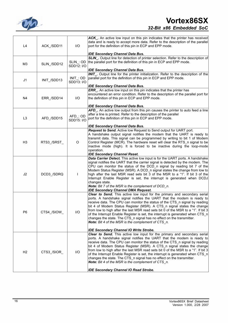
L4 ACK_/SDD11 I/O
ACK_. An active low input on this pin indicates that the printer has received data and is ready to accept more data. Refer to the description of the parallel port for the definition of this pin in ECP and EPP mode. IDE Secondary Channel Data Bus.
M3 SLIN_/SDD12 SLIN_: OD SDD12: I/O
SLIN_. Output line for detection of printer selection. Refer to the description of the parallel port for the definition of this pin in ECP and EPP mode. IDE Secondary Channel Data Bus.
J1 INIT_/SDD13 INIT_: OD SDD13: I/O
INIT_. Output line for the printer initialization. Refer to the description of the parallel port for the definition of this pin in ECP and EPP mode. IDE Secondary Channel Data Bus.
N4 ERR_/SDD14 I/O
ERR_. An active low input on this pin indicates that the printer has encountered an error condition. Refer to the description of the parallel port for the definition of this pin in ECP and EPP mode. IDE Secondary Channel Data Bus.
L3 AFD_/SDD15 AFD_: OD SDD15: I/O
AFD_. An active low output from this pin causes the printer to auto feed a line after a line is printed. Refer to the description of the parallel port for the definition of this pin in ECP and EPP mode. IDE Secondary Channel Data Bus.
H3 RTS3_/SRST_ O
Request to Send. Active low Request to Send output for UART port. A handshake output signal notifies the modem that the UART is ready to transmit data. This signal can be programmed by writing to bit 1 of Modem Control Register (MCR). The hardware reset will clear the RTS_n signal to be inactive mode (high). It is forced to be inactive during the loop-mode operation. IDE Secondary Channel Reset.
J2 DCD3_/SDRQ I
Data Carrier Detect. This active low input is for the UART ports. A handshake signal notifies the UART that the carrier signal is detected by the modem. The CPU can monitor the status of the DCD_n signal by reading bit 7 of the Modem Status Register (MSR). A DCD_n signal states the change from low to high after the last MSR read sets bit 3 of the MSR to a “1”. If bit 3 of the Interrupt Enable Register is set, the interrupt is generated when DCDJ changes state. Note: Bit 7 of the MSR is the complement of DCD_n. IDE Secondary Channel DMA Request.
P6 CTS4_/SIOW_ I/O
Clear to Send. This active low input for the primary and secondary serial ports. A handshake signal notifies the UART that the modem is ready to receive data. The CPU can monitor the status of the CTS_n signal by reading bit 4 of Modem Status Register (MSR). A CTS_n signal states the change from low to high after the last MSR read sets bit 0 of the MSR to a “1”. If bit 3 of the Interrupt Enable Register is set, the interrupt is generated when CTS_n changes the state. The CTS_n signal has no effect on the transmitter. Note: Bit 4 of the MSR is the complement of CTS_n. IDE Secondary Channel IO Write Strobe.
H2 CTS3_/SIOR_ I/O
Clear to Send. This active low input for the primary and secondary serial ports. A handshake signal notifies the UART that the modem is ready to receive data. The CPU can monitor the status of the CTS_n signal by reading bit 4 of Modem Status Register (MSR). A CTS_n signal states the change from low to high after the last MSR read sets bit 0 of the MSR to a “1”. If bit 3 of the Interrupt Enable Register is set, the interrupt is generated when CTS_n changes the state. The CTS_n signal has no effect on the transmitter. Note: Bit 4 of the MSR is the complement of CTS_n. IDE Secondary Channel IO Read Strobe.
Vortex86SX 32-Bit x86 Embedded SoC
Vortex86SX Brief Datasheet Version 1.000, 2/28, 2007
17
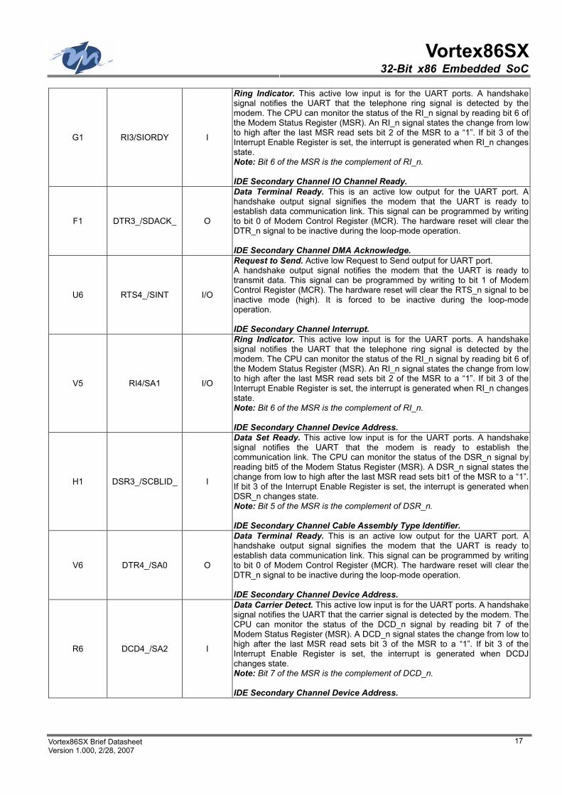
G1 RI3/SIORDY I
Ring Indicator. This active low input is for the UART ports. A handshake signal notifies the UART that the telephone ring signal is detected by the modem. The CPU can monitor the status of the RI_n signal by reading bit 6 of the Modem Status Register (MSR). An RI_n signal states the change from low to high after the last MSR read sets bit 2 of the MSR to a “1”. If bit 3 of the Interrupt Enable Register is set, the interrupt is generated when RI_n changes state. Note: Bit 6 of the MSR is the complement of RI_n. IDE Secondary Channel IO Channel Ready.
F1 DTR3_/SDACK_ O
Data Terminal Ready. This is an active low output for the UART port. A handshake output signal signifies the modem that the UART is ready to establish data communication link. This signal can be programmed by writing to bit 0 of Modem Control Register (MCR). The hardware reset will clear the DTR_n signal to be inactive during the loop-mode operation. IDE Secondary Channel DMA Acknowledge.
U6 RTS4_/SINT I/O
Request to Send. Active low Request to Send output for UART port. A handshake output signal notifies the modem that the UART is ready to transmit data. This signal can be programmed by writing to bit 1 of Modem Control Register (MCR). The hardware reset will clear the RTS_n signal to be inactive mode (high). It is forced to be inactive during the loop-mode operation. IDE Secondary Channel Interrupt.
V5 RI4/SA1 I/O
Ring Indicator. This active low input is for the UART ports. A handshake signal notifies the UART that the telephone ring signal is detected by the modem. The CPU can monitor the status of the RI_n signal by reading bit 6 of the Modem Status Register (MSR). An RI_n signal states the change from low to high after the last MSR read sets bit 2 of the MSR to a “1”. If bit 3 of the Interrupt Enable Register is set, the interrupt is generated when RI_n changes state. Note: Bit 6 of the MSR is the complement of RI_n. IDE Secondary Channel Device Address.
H1 DSR3_/SCBLID_ I
Data Set Ready. This active low input is for the UART ports. A handshake signal notifies the UART that the modem is ready to establish the communication link. The CPU can monitor the status of the DSR_n signal by reading bit5 of the Modem Status Register (MSR). A DSR_n signal states the change from low to high after the last MSR read sets bit1 of the MSR to a “1”. If bit 3 of the Interrupt Enable Register is set, the interrupt is generated when DSR_n changes state. Note: Bit 5 of the MSR is the complement of DSR_n. IDE Secondary Channel Cable Assembly Type Identifier.
V6 DTR4_/SA0 O
Data Terminal Ready. This is an active low output for the UART port. A handshake output signal signifies the modem that the UART is ready to establish data communication link. This signal can be programmed by writing to bit 0 of Modem Control Register (MCR). The hardware reset will clear the DTR_n signal to be inactive during the loop-mode operation. IDE Secondary Channel Device Address.
R6 DCD4_/SA2 I
Data Carrier Detect. This active low input is for the UART ports. A handshake signal notifies the UART that the carrier signal is detected by the modem. The CPU can monitor the status of the DCD_n signal by reading bit 7 of the Modem Status Register (MSR). A DCD_n signal states the change from low to high after the last MSR read sets bit 3 of the MSR to a “1”. If bit 3 of the Interrupt Enable Register is set, the interrupt is generated when DCDJ changes state. Note: Bit 7 of the MSR is the complement of DCD_n. IDE Secondary Channel Device Address.
Vortex86SX 32-Bit x86 Embedded SoC
Vortex86SX Brief Datasheet
Version 1.000, 2/28 2007 18
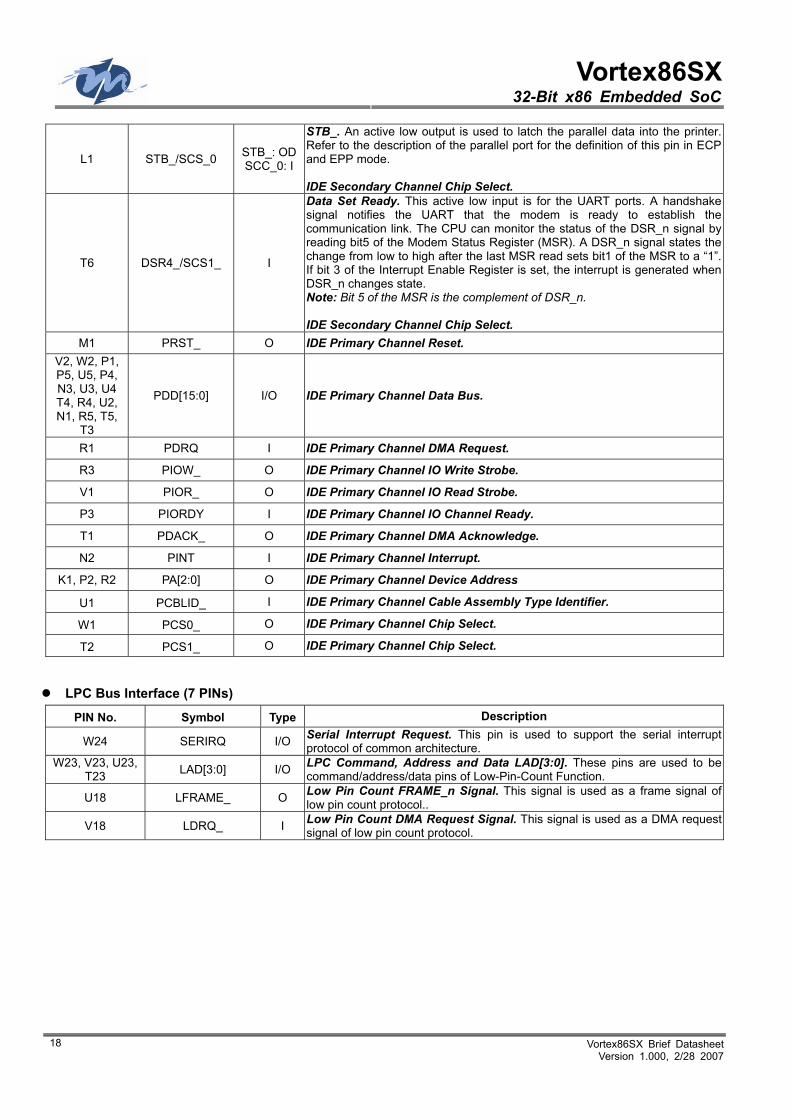
L1 STB_/SCS_0 STB_: OD SCC_0: I
STB_. An active low output is used to latch the parallel data into the printer. Refer to the description of the parallel port for the definition of this pin in ECP and EPP mode. IDE Secondary Channel Chip Select.
T6 DSR4_/SCS1_ I
Data Set Ready. This active low input is for the UART ports. A handshake signal notifies the UART that the modem is ready to establish the communication link. The CPU can monitor the status of the DSR_n signal by reading bit5 of the Modem Status Register (MSR). A DSR_n signal states the change from low to high after the last MSR read sets bit1 of the MSR to a “1”. If bit 3 of the Interrupt Enable Register is set, the interrupt is generated when DSR_n changes state. Note: Bit 5 of the MSR is the complement of DSR_n. IDE Secondary Channel Chip Select.
M1 PRST_ O IDE Primary Channel Reset. V2, W2, P1, P5, U5, P4, N3, U3, U4 T4, R4, U2, N1, R5, T5,
T3
PDD[15:0] I/O IDE Primary Channel Data Bus.
R1 PDRQ I IDE Primary Channel DMA Request.
R3 PIOW_ O IDE Primary Channel IO Write Strobe.
V1 PIOR_ O IDE Primary Channel IO Read Strobe.
P3 PIORDY I IDE Primary Channel IO Channel Ready.
T1 PDACK_ O IDE Primary Channel DMA Acknowledge.
N2 PINT I IDE Primary Channel Interrupt.
K1, P2, R2 PA[2:0] O IDE Primary Channel Device Address
U1 PCBLID_ I IDE Primary Channel Cable Assembly Type Identifier.
W1 PCS0_ O IDE Primary Channel Chip Select.
T2 PCS1_ O IDE Primary Channel Chip Select.
LPC Bus Interface (7 PINs)
PIN No. Symbol Type Description
W24 SERIRQ I/O Serial Interrupt Request. This pin is used to support the serial interrupt protocol of common architecture.
W23, V23, U23, T23 LAD[3:0] I/O LPC Command, Address and Data LAD[3:0]. These pins are used to be
command/address/data pins of Low-Pin-Count Function.
U18 LFRAME_ O Low Pin Count FRAME_n Signal. This signal is used as a frame signal of low pin count protocol..
V18 LDRQ_ I Low Pin Count DMA Request Signal. This signal is used as a DMA request signal of low pin count protocol.
Vortex86SX 32-Bit x86 Embedded SoC
Vortex86SX Brief Datasheet Version 1.000, 2/28, 2007
19
GPIO Interface (24 PINs)
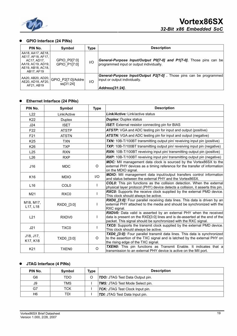
PIN No. Symbol Type Description AA18, AA17, AE18, AE17, AF18, AF17,
AC17, AD17, AA19, AC19, AD19, AE19, AB18, AC18,
AB17, AF19
GPIO_P0[7:0] GPIO_P1[7:0] I/O General-Purpose Input/Output P0[7-0] and P1[7-0]. Those pins can be
programmed input or output individually.
AA20, AB20, AD20, AE20, AD18, AF20,
AF21, AB19
GPIO_P2[7:0]/Address[31:24] I/O
General-Purpose Input/Output P2[7-0] . Those pins can be programmed input or output individually. Address[31:24].
Ethernet Interface (24 PINs)
PIN No. Symbol Type Description
L22 Link/Active Link/Active: Link/active status K22 Duplex Duplex: Duplex status J24 ISET ISET: External resistor connecting pin for BIAS F22 ATSTP ATSTP: VGA and ADC testing pin for input and output (positive) F21 ATSTN ATSTN: VGA and ADC testing pin for input and output (negative) K25 TXN TXN: 10B-T/100BT transmitting output pin/ reveiving input pin (positive) K26 TXP TXP: 10B-T/100BT transmitting output pin/ reveiving input pin (negative)L25 RXN RXN: 10B-T/100BT reveiving input pin/ transmitting output pin (positive) L26 RXP RXP: 10B-T/100BT reveiving input pin/ transmitting output pin (negative)
J16 MDC O MDC: MII management data clock is sourced by the Vortex86SX to the external PHY devices as a timing reference for the transfer of information on the MDIO signal.
K16 MDIO I/O MDIO: MII management data input/output transfers control information and status between the external PHY and the Vortex86SX.
L16 COL0 I COL0: This pin functions as the collision detection. When the external physical layer protocol (PHY) device detects a collision, it asserts this pin.
M21 RXC0 I RXC0: Supports the receive clock supplied by the external PMD device. This clock should always be active.
M18, M17, L17, L18 RXD0_[3:0] I
RXD0_[3:0]: Four parallel receiving data lines. This data is driven by an external PHY attached to the media and should be synchronized with the RXC signal.
L21 RXDV0 I RXDV0: Data valid is asserted by an external PHY when the received data is present on the RXD[3:0] lines and is de-asserted at the end of the packet. This signal should be synchronized with the RXC signal.
J21 TXC0 I TXC0: Supports the transmit clock supplied by the external PMD device. This clock should always be active.
J18, J17, K17, K18
TXD0_[3:0] O TXD0_[3:0]: Four parallel transmit data lines. This data is synchronized to the assertion of the TXC signal and is latched by the external PHY on the rising edge of the TXC signal.
K21 TXEN0 O TXEN0: This pin functions as Transmit Enable. It indicates that a transmission to an external PHY device is active on the MII port.
JTAG Interface (4 PINs)
PIN No. Symbol Type Description
G6 TDO O TDO: JTAG Test Data Output pin.
J9 TMS I TMS: JTAG Test Mode Select pin. G7 TCK I TCK: JTAG Test Clock Input pin. H6 TDI I TDI: JTAG Test Data Input pin.
Vortex86SX 32-Bit x86 Embedded SoC
Vortex86SX Brief Datasheet
Version 1.000, 2/28 2007 20
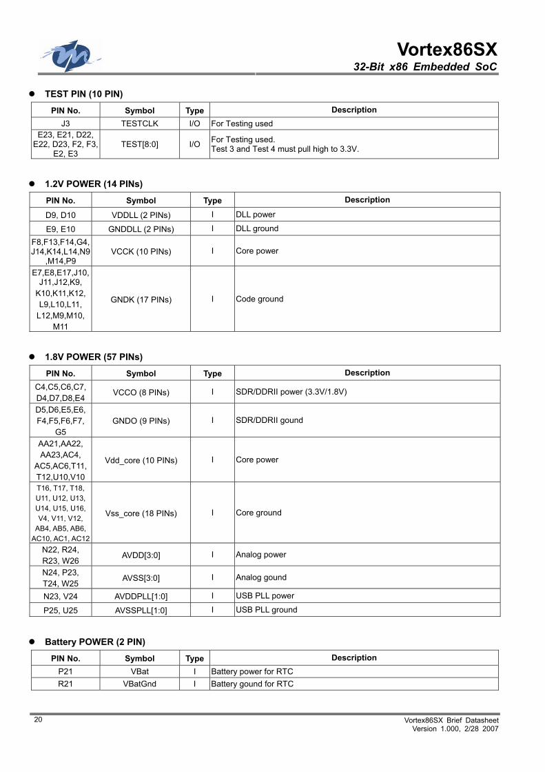
TEST PIN (10 PIN)
PIN No. Symbol Type Description J3 TESTCLK I/O For Testing used
E23, E21, D22, E22, D23, F2, F3,
E2, E3 TEST[8:0] I/O For Testing used.
Test 3 and Test 4 must pull high to 3.3V.
1.2V POWER (14 PINs)
PIN No. Symbol Type Description
D9, D10 VDDLL (2 PINs) I DLL power
E9, E10 GNDDLL (2 PINs) I DLL ground F8,F13,F14,G4,J14,K14,L14,N9
,M14,P9 VCCK (10 PINs) I Core power
E7,E8,E17,J10,J11,J12,K9,
K10,K11,K12, L9,L10,L11,
L12,M9,M10, M11
GNDK (17 PINs) I Code ground
1.8V POWER (57 PINs)
PIN No. Symbol Type Description C4,C5,C6,C7, D4,D7,D8,E4
VCCO (8 PINs) I SDR/DDRII power (3.3V/1.8V)
D5,D6,E5,E6, F4,F5,F6,F7,
G5 GNDO (9 PINs) I SDR/DDRII gound
AA21,AA22, AA23,AC4,
AC5,AC6,T11, T12,U10,V10
Vdd_core (10 PINs) I Core power
T16, T17, T18, U11, U12, U13, U14, U15, U16, V4, V11, V12,
AB4, AB5, AB6, AC10, AC1, AC12
Vss_core (18 PINs) I Core ground
N22, R24, R23, W26
AVDD[3:0] I Analog power
N24, P23, T24, W25
AVSS[3:0] I Analog gound
N23, V24 AVDDPLL[1:0] I USB PLL power
P25, U25 AVSSPLL[1:0] I USB PLL ground
Battery POWER (2 PIN)
PIN No. Symbol Type Description P21 VBat I Battery power for RTC R21 VBatGnd I Battery gound for RTC
Vortex86SX 32-Bit x86 Embedded SoC
Vortex86SX Brief Datasheet Version 1.000, 2/28, 2007
21
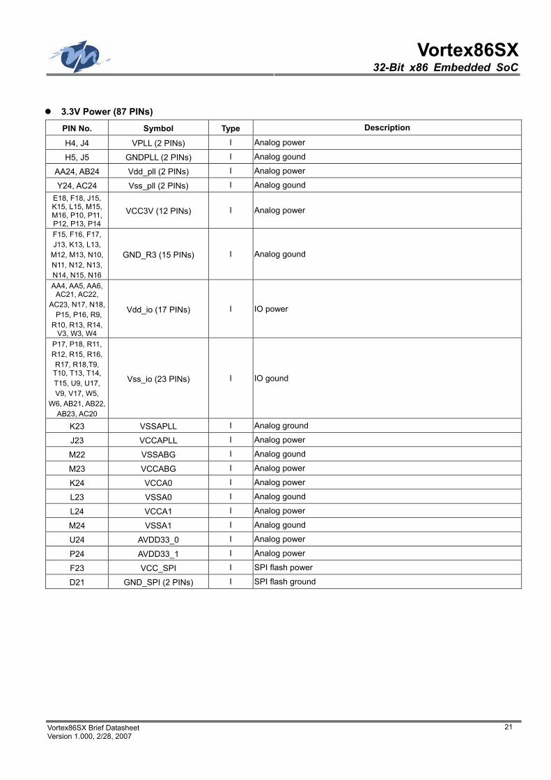
3.3V Power (87 PINs)
PIN No. Symbol Type Description
H4, J4 VPLL (2 PINs) I Analog power
H5, J5 GNDPLL (2 PINs) I Analog gound
AA24, AB24 Vdd_pll (2 PINs) I Analog power
Y24, AC24 Vss_pll (2 PINs) I Analog gound E18, F18, J15, K15, L15, M15, M16, P10, P11, P12, P13, P14
VCC3V (12 PINs) I Analog power
F15, F16, F17, J13, K13, L13,
M12, M13, N10, N11, N12, N13, N14, N15, N16
GND_R3 (15 PINs) I Analog gound
AA4, AA5, AA6, AC21, AC22,
AC23, N17, N18, P15, P16, R9, R10, R13, R14,
V3, W3, W4
Vdd_io (17 PINs) I IO power
P17, P18, R11, R12, R15, R16, R17, R18,T9,
T10, T13, T14, T15, U9, U17, V9, V17, W5,
W6, AB21, AB22, AB23, AC20
Vss_io (23 PINs) I IO gound
K23 VSSAPLL I Analog ground
J23 VCCAPLL I Analog power
M22 VSSABG I Analog gound
M23 VCCABG I Analog power
K24 VCCA0 I Analog power
L23 VSSA0 I Analog gound
L24 VCCA1 I Analog power
M24 VSSA1 I Analog gound
U24 AVDD33_0 I Analog power
P24 AVDD33_1 I Analog power
F23 VCC_SPI I SPI flash power
D21 GND_SPI (2 PINs) I SPI flash ground
5 5
4 4
3 3
2 2
1 1
DD
CC
BB
AA
ISA
BU
SPC
I BU
S
Vor
tex8
6SX
SO
C R
efer
ence
Des
ign
1.1
Vor
tex8
6SX
PC
I/IS
A B
US
DM
P EL
ECTR
ON
ICS
INC
.
28
Mon
day,
Jan
uary
29,
200
7
Title
Size
Doc
umen
t Num
ber
Rev
Dat
e:S
heet
of
SA
0S
A1
SA
2S
A3
SA
5S
A6
SA
7S
A8
SA
9S
A10
SA
11S
A12
SA
13S
A14
SA
15S
A16
SA
17S
A18
SA
19
LA17
LA18
LA19
LA20
LA21
LA22
LA23
DR
Q0
DR
Q1
DR
Q2
DR
Q3
DR
Q5
DR
Q6
DR
Q7
DA
CK
0D
AC
K1
DA
CK
2D
AC
K3
DA
CK
5D
AC
K6
DA
CK
7
TCRE
FRE
SH
ME
MC
S16
IOC
S16
MEM
WR
STD
RV
IOC
HC
KA
EN
SB
HE
MEM
R
IRQ
14IR
Q15
IOC
HR
DY
IRQ
9IR
Q10
IRQ
11IR
Q12
IRQ
4IR
Q5
IRQ
6IR
Q7
IRQ
3
OW
SS
MEM
RSM
EMW
IOW
IOR
SA
4
SA
[0..1
9]
SD
[0..1
5]
SD
8
SD
1
SD
9
SD
3
SD
15
SD
4
SD
7
SD
11S
D12
SD
13
SD
5
SD
0
SD
10
SD
6
SD
14
SD
2
GP
CS
0G
PC
S1
BA
LE
PC
ICLK
1
INT-
B
CB
E-2
AD
27
PG
NT-
0
AD
30IN
T-C
AD
25
AD
19
INT-
D
STO
P-
AD
22
AD
5
AD
17
AD
31
AD
4
AD
29
AD
14
AD
23
AD
16
AD
2
PC
ICLK
1RCB
E-1
AD
18
AD
8A
D7
AD
10
DE
VS
EL-
CB
E-3
AD
28
AD
15
AD
13
AD
3
AD
[0..3
1]
INT-
A
PA
R
FRA
ME
-A
D21
IRD
Y-
TRD
Y-
CB
E-0
PR
EQ
-0
AD
11
AD
6
AD
1
AD
24
AD
20
AD
12
AD
0
AD
26
AD
9
PC
IRS
T-
AD
[0..3
1]8
SMEM
W8
MEM
W8
IRQ
128
IRQ
148
IOC
S16
8
RE
FRE
SH
8
IRQ
38
SB
HE
8
IOW
8
IRQ
58
IRQ
68
IRQ
98
IRQ
78
ME
MC
S16
8
IOR
8
IRQ
118
IRQ
158
RS
TDR
V8
MEM
R8
BA
LE8
IRQ
48
SM
EMR
8O
WS
8
AE
N8
IRQ
108
TC8
IOC
HR
DY
8D
RQ
08
SD
[0..1
5]8
SA
[0..1
9]8
IOC
HC
K8
DR
Q1
8D
RQ
28
DR
Q3
8D
RQ
58
DR
Q6
8D
RQ
78
DA
CK
08
DA
CK
18
DA
CK
28
DA
CK
38
DA
CK
58
DA
CK
68
DA
CK
78
LA17
8LA
188
LA19
8LA
208
LA21
8LA
228
LA23
8
FRA
ME
-8
TRD
Y-
8
STO
P-8
CB
E-0
8C
BE
-18
CB
E-2
8C
BE
-38
PC
IRS
T-8
PG
NT-
08
PR
EQ
-08
IRD
Y-
8
PA
R8
DE
VS
EL-
8
INT-
A8
INT-
B8
INT-
C8
INT-
D8
GP
CS
04
GP
CS
14
OS
C8
SY
SC
LK8
PC
ICLK
18
R22
22
U1C
Vor
tex8
6SX
H24
J26
J25
H26
H25
G26
J22
G25
H21
F25
F26
G23
H22
E26
E25
E24
B23
C23
B22
C22
B21
C21
E20
D20
B26
A25
A24
A23
A22
A21
B20
C20
C18
B18
B19
C19
D18
D19 F24
G22
B24
B25
A19
A18
A20
D26
C24
C25
C26
D24
D25
G24
H23 F19
F20
E19
AD
00A
D01
AD
02A
D03
AD
04A
D05
AD
06A
D07
AD
08A
D09
AD
10A
D11
AD
12A
D13
AD
14A
D15
AD
16A
D17
AD
18A
D19
AD
20A
D21
AD
22A
D23
AD
24A
D25
AD
26A
D27
AD
28A
D29
AD
30A
D31
PR
EQ
0P
RE
Q1
PR
EQ
2
PG
NT0
PG
NT1
PG
NT2
CB
E0
CB
E1
CB
E2
CB
E3
PC
ICLK
0
PC
ICLK
1
PC
ICLK
2
-PC
IRS
T
-FR
AM
E-IR
DY
-TR
DY
-DE
VS
EL
-STO
PP
AR
-INTA
-INTB
-INTC
-INTD
U1B
Vor
tex8
6SX
AA
7Y
1A
C14
AA
16A
A14 Y4
AD
14 Y6
AD
12A
E10
AE
11A
F14
AF1
5A
D10
AF1
6A
E16
AC
3A
F12
AB
13A
A12
AB
11A
E13
AC
2A
D6
AC
7A
E5
AB
7A
D3
AA
2A
D2
AB
2A
A1
AA
3A
B9
AD
5A
A9
AE
9A
B15
AD
15A
A15
AE
14A
D13
AC
15
AB
12A
D4
AC
9Y
5A
A11
AF1
1A
E15
AE
2A
D1
AD
7A
C1
AE
7A
B14
AE
6A
F3A
C8
AF2
AF4
AD
9A
B3
AF1
3Y
3A
B10
AD
11A
F7
AE
8A
A13
AB
8A
C13
AF9
AE
12A
B1
AD
8A
A10
AA
8Y
2A
B16
AF6
AF1
0A
F5A
E4
AE
1A
E3
AF8
AC
16A
D16
G21
SD
00S
D01
SD
02S
D03
SD
04S
D05
SD
06S
D07
SD
08S
D09
SD
10S
D11
SD
12S
D13
SD
14S
D15
SA
00S
A01
SA
02S
A03
SA
04S
A05
SA
06S
A07
SA
08S
A09
SA
10S
A11
SA
12S
A13
SA
14S
A15
SA
16S
A17
SA
18S
A19
LA17
LA18
LA19
LA20
LA21
LA22
LA23
DR
Q0
DR
Q1
DR
Q2
DR
Q3
DR
Q5
DR
Q6
DR
Q7
IRQ
03IR
Q04
IRQ
05IR
Q06
IRQ
07IR
Q09
IRQ
10IR
Q11
IRQ
12IR
Q14
IRQ
15
DA
CK
0D
AC
K1
DA
CK
2D
AC
K3
DA
CK
5D
AC
K6
DA
CK
7
-IOC
HR
DY
-IOC
HC
KA
EN
-SB
HE
-ME
MR
-ME
MW
RS
ET_
DR
V-0
WS
-SM
EM
R-S
ME
MW
-IOW
-IOR
-RE
FRE
SH
SY
SC
LKTCB
ALE
-ME
MC
S16
-IOC
S16
OS
C14
M-G
PC
S0
-GP
CS
1-R
OM
CS
R23
22TP
1
R21
22
5 5
4 4
3 3
2 2
1 1
DD
CC
BB
AA
USB
x2
LAN
LINK
TX/RX
USB
x2
LAN
USB
x4
RJ4
5
Vor
tex8
6SX
SO
C R
efer
ence
Des
ign
1.1
Vor
tex8
6SX
LA
N/U
SB
DM
P EL
ECTR
ON
ICS
INC
.
38
Mon
day,
Jan
uary
29,
200
7
Title
Size
Doc
umen
t Num
ber
Rev
Dat
e:S
heet
of
AV
DD
0
AV
DD
1
AV
DD
3
AV
DD
PLL
0
AV
DD
PLL
1
AV
DD
33
VC
CA
PLL
VC
CA
BG
VC
CA
0
US
BD
0+U
SB
D0-
US
BD
1+U
SB
D1-
US
BD
2+U
SB
D2-
US
BD
3+U
SB
D3-
LUS
BD
0-LU
SB
D1-
LUS
BD
1+
LUS
BD
2-LU
SB
D2+
TXD
+
ARX+
DU
PLE
X
TXD
-
ATX+
ATX-
LIN
K/A
CTI
VE
CC
MT
ARX-
RX
IN-
RX
IN+
CC
T
TXD
+TX
D-
RX
IN+
RX
IN-
LIN
K/A
CTI
VE
DU
PLE
X
VC
CA
PLL
VC
CA
BG
VC
CA
0
AV
DD
0
AV
DD
1
AV
DD
3
AV
DD
PLL
0
AV
DD
PLL
1
AV
DD
33
LUS
BD
3-LU
SB
D3+LU
SB
D0+
US
BD
2-LU
SB
D2-
LUS
BD
2+U
SB
D2+
LUS
BD
0-
LUS
BD
0+
US
BD
0-
US
BD
0+
LUS
BD
1-
LUS
BD
1+
US
BD
1-
US
BD
1+
LUS
BD
3-
LUS
BD
3+U
SB
D3+
US
BD
3-
GGND
GGND
VC
C
GGND
GGND
VC
C3
VC
C3
VC
C1.
8V
CC
1.8
VC
C1.
8V
CC
1.8
VC
C1.
8
VC
C3
VC
C3
GGNDV
CC
VC
C
L2
SF2
0129
00Y
SB
1
4 2
3
R28
1K
R24
6.19
K 1
%
C22
104
C23
103
R32
50C
11
104
C1
104
L4
SF2
0129
00Y
SB1
4 2
3
F2LP
-ISM
110
0805
C9
104
C3
104
U3
TS61
21A
6 8 7 3 2 1
11 10 9 14 15 16
RD
+
RD
-
CT
TD-
CT
TD+
RX
+
CT
RX
-
TX-
CM
T
TX+
L1
SF2
0129
00Y
SB
1
42
3
C5
104
C21
103
L7B
EA
D
US
B1A
1
UL-
1
U1
U2
U3
U4
H5
H6
U5
U6
U7
U8
H3
H4
VC
C-D
ATA
+DA
TAG
ND
HO
LEH
OLE
VC
C-D
ATA
+DA
TAG
ND
HO
LEH
OLE
L5B
EA
D
C8
103
C14
104
L10
BE
AD
J2
HE
AD
ER
5X
2/B
OX
12
34
56
78
910
R31
50
R25
510
L6B
EA
D
R35
75
C6
103
U1F
Vor
tex8
6SX
W26
R23
R24
N22
W25
T24
P23
N24
V24
N23
U25
P25
U24
P24
T26
R26
N26
M26
T25
R25
N25
M25
U26
P26
L22
K22 J23
K23
M22
M23
K24 L24
L23
M24J24
F22
F21
K26
K25 L26
L25
M18
M17L17
L18
J18
J17
K17
K18 L21
L16
K16 J16
M21J21
K21
AB
26
AV
DD
0
AV
DD
1
AV
DD
2
AV
DD
3
AV
SS
0
AV
SS
1
AV
SS
2
AV
SS
3
AV
DD
PLL
0
AV
DD
PLL
1
AV
SS
PLL
0
AV
SS
PLL
1
AV
DD
33_0
AV
DD
33_1
DP
0
DP
1
DP
2
DP
3
DM
0
DM
1
DM
2
DM
3
RE
XT0
RE
XT1
Link
/Act
ive
Dup
lex
VC
CA
PLL
VS
SA
PLL
VS
SA
BG
VC
CA
BG
VC
CA
0
VC
CA
1
VS
SA
0
VS
SA
1
ISE
T
ATS
TPA
TSTN
TXP
TXN
RX
PR
XN
RX
D03
RX
D02
RX
D01
RX
D00
TXD
03TX
D02
TXD
01TX
D00
RX
DV
0
CO
L0
MD
IOM
DC
RX
C0
TXC
0TX
EN
0C
LK25
MO
UT
C10
103
C7
104
R29
50
L13
BE
AD
R26
510
C13
104
C2
103
L8B
EA
D
L12
BE
AD
R30
50
C19
103
R27
1K
C12
103
R36
75
L9B
EA
D
L11
BE
AD
F1LP
-ISM
110
0805
R34
75
C18
104
C15
104
C4
103
C16
104
US
B1B
1
UL-
2
H1
H2
L10
L12 L8L7L6 L5 L4L3 L2L1
L9 L11
HO
LEH
OLE
PLE
D0
PLE
D1
NC
NC
RO
-N
CN
C
RO
+
TD-
TD+
VC
CV
CC
C20
104
R33
75
L3
SF2
0129
00Y
SB1
42
3
C17
102/
3KV
5 5
4 4
3 3
2 2
1 1
DD
CC
BB
AA
SPEA
KER
KB
D
MOUSE
KB
D/M
OU
SE
JTA
G
POW
ER G
OO
D
RED
UN
DA
NC
Y
LPC
BU
S
MTB
F LE
D
POW
ER L
ED
JTA
G
Vor
tex8
6SX
SO
C R
efer
ence
Des
ign
1.1
Vor
tex8
6SX
KB
D/M
S/L
PC
/JTA
G
DM
P EL
ECTR
ON
ICS
INC
.
48
Mon
day,
Jan
uary
29,
200
7
Title
Size
Doc
umen
t Num
ber
Rev
Dat
e:S
heet
of
VP
LL0
VD
LL0
VD
DP
LL0
TDO
TDI
TCK
TMS VP
LL0
VD
LL0
PW
RG
D
KB
CLK
KB
DA
TAM
SC
LKM
SD
ATA
RX
D9\
TXD
9\
SY
S-F
AIL
-INS
YS
-FA
IL-O
UT
SY
S-S
W-IN
SY
S-G
PC
S-IN
SP
EA
KE
R
SP
EA
KE
R
KB
DA
TA
MS
CLK
MS
DAT
A
MTB
F-O
UT
TMS
TDO
TDI
KB
CLK
PW
RG
D
SY
S-F
AIL
-OU
TTX
D9\
GP
CS
0
RX
D9\
SY
S-F
AIL
-INS
YS
-GP
CS
-INS
YS
-SW
-IN
XY
2
XY
1
XX
1
XX
2
GP
CS
1
VD
DP
LL0
TCK
MTB
F-O
UT
GP
CS
02
GP
CS
12
PW
RG
D6
VC
C1.
2
VC
C3
VC
C3
VC
C
VC
C
GGND
VC
C
VC
C3
VC
C3
VBAT
VC
C3
VC
C3
VC
C3
VC
C
VC
C
VC
C
L14
BE
AD
R42
330
C40
104
C33
47pF
LED
3
LED
-SM
D
AC
C34
47pFL1
6B
EA
D
C41
103
J4 HE
AD
ER
2
1 2
D1
FM16
0A
C
C30
104
C26
22pF
F3LP
-ISM
110
0805
J5 PS
/2 K
B/M
S
1 2 3 4 5 6 7 8 9 10 11 12
13 14 15 16 17
J3
HE
AD
ER
5-1
.25m
m
1 2 3 4 5
L19
BE
AD
J6
HE
AD
ER
5X
2-2.
0mm
12
34
56
78
910
R39
1M R40
1M
R38
1K
C25
104
U1G
Vor
tex8
6SX
AA
26
Y26
Y25
AA
25
AB
25U
21U
22V
22V
21
V13
V16
V14
V15
R21
P21
V26
V25
W24
T23
U23
V23
W23
U18
V18
G6
H6
G7
J9 J3 D23
E22
D22
E21
E23
D10
D9
E10
E9
H4
J4H5
J5AB
24
AA
24
AC
24
Y24
E3 F3E2F2K6 J6
Y23
PO
WE
R_G
OO
D
XO
UT_
1431
8
XIN
_143
18
MTB
F
CLK
24M
Out
-Ext
Sys
FailI
n-S
YS
FAIL
Out
Ext
_Sw
itch_
fail
EX
T_G
PC
S
KB
CLK
/-KB
RS
TK
BD
ATA
/-A20
GA
TEM
SC
LKM
SD
ATA
VB
atG
nd
VB
at
RTC
_Xin
RTC
_Xou
t
SE
RIR
Q
LAD
0LA
D1
LAD
2LA
D3
-LFR
AM
E-L
DR
Q
TDO
TDI
TCK
TMS
TES
TCLK
TES
T0TE
ST1
TES
T2TE
ST3
TES
T4
VD
LL0
VD
LL1
GN
DD
LL0
GN
DD
LL1
VP
LL0
VP
LL1
GN
DP
LL0
GN
DP
LL1
Vdd
_pll_
0
Vdd
_pll_
1
Vss
_pll_
0
Vss
_pll_
1
N2S
S2N
-GN
Tx-R
EQ
x
SIN
9S
OU
T9
SP
EA
KE
R
C31
47pF
C28
22pF
RN
2010
Kx4
1 23 45 67 8
D2
1N41
48A
C
R46
1K
L15
BE
AD
L18
BE
AD C
38
104
R37
1K
U4
MAX
809S
V
R G
VC
C
-RS
T
GN
D
C32
47pF
Q1
3904
C36
104
BT1
CR
2354
+ -
L17
BE
AD
SP
1
BU
ZZE
RR
444.
7K
C39
103
R45
1KLE
D2
LED
-SM
D
AC
Y1
14.3
18M
Hz
12
C27
22pF
C24
10pF
L20
BE
AD
Y2
32.7
68K
Hz
12
C37
103
C29
22pF
R41
4.7K
R43
22
RN
1910
Kx4
1 23 45 67 8
C35
104
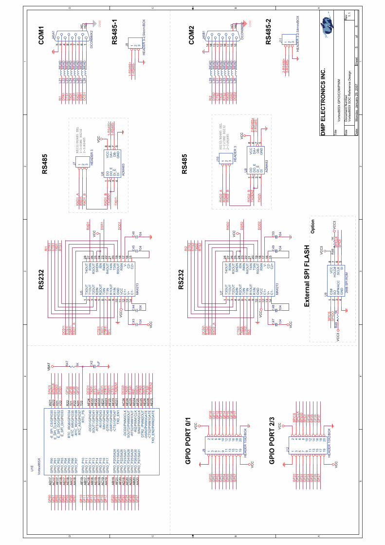
5 5
4 4
3 3
2 2
1 1
DD
CC
BB
AA
1-2:COM1 RS232
2-3:RS485
RS232/RS485 SEL
RS4
85-2
2-3:RS485
RS232/RS485 SEL
1-2:COM2 RS232
RS4
85-1
CO
M1
CO
M2
RS2
32
RS2
32G
PIO
PO
RT
0/1
GPI
O P
OR
T 2/
3
RS4
85
RS4
85
Exte
rnal
SPI
FLA
SHO
ptio
n
Vor
tex8
6SX
SO
C R
efer
ence
Des
ign
1.1
Vor
tex8
6SX
GP
IO/C
OM
/PW
M
DM
P EL
ECTR
ON
ICS
INC
.
58
Mon
day,
Jan
uary
29,
200
7
Title
Size
Doc
umen
t Num
ber
Rev
Dat
e:S
heet
of
GP
00G
P01
GP
02G
P03
GP
04G
P05
GP
06G
P07
GP
10G
P11
GP
12G
P13
GP
14G
P15
GP
17
GP
20G
P21
GP
22G
P23
GP
24G
P25
GP
26G
P27
SP
ICS
SP
ICLK
SP
IDO
SP
IDI
GP
34G
P35
GP
36G
P37
DC
D1\
TXD
1\R
TS1\
RI1
\R
XD
1\D
TR1\
DS
R1\
CTS
1\TX
DEN
1
GP
16
GP
00G
P01
GP
02G
P03
GP
04G
P05
GP
06G
P07
GP
15
GP
12
GP
14
GP
10
GP
13
GP
17
GP
11
GP
16
RI1
\
DC
D1\
DTR
1\
DS
R1\
CTS
1
RX
D1
TXD
1\
DTR
1
RTS
1\
TXD
1
CTS
1\
RX
D1_
A
DC
D1
DS
R1
RI1
DTR
1
DC
D1
RTS
1
RTS
1R
I1
DC
D2\
DTR
2\
RX
D2
RTS
2\
RX
D2_
A
DC
D2
TXD
2\C
TS2\
DS
R2
RI2
\
DS
R2\
CTS
2
RTS
2
DTR
2R
I2
TXD
2
RTS
2
DC
D2
CTS
2D
TR2
DS
R2
TXD
2
RX
D2
RI2
RX
D1_
A
1-R
S48
5+TX
DEN
1R
XD
1_B
1-R
S48
5-
RX
D1_
B
TXD
1\
RX
D1\
2-R
S48
5-2-
RS
485+
TXD
2\
RX
D2_
B
2-R
S48
5-TX
DEN
2
RX
D2_
A
RX
D2_
B
2-R
S48
5+
RX
D2\
1-R
S48
5+1-
RS
485-
GP
25G
P24
GP
36G
P26
GP
27
SP
IDO
GP
35
GP
23G
P34
GP
20G
P21
SP
ICLK
SP
ICS
GP
37
GP
22S
PID
I
DS
R1
TXD
1C
TS1
RX
D1
DC
D2\
TXD
2\R
TS2\
RI2
\R
XD
2\D
TR2\
DS
R2\
CTS
2\TX
DEN
2
SP
ICS
SP
IDO
SP
IDI
SP
ICLK
VC
C
VC
C
VC
C
VC
C
VC
C
VC
C
GGND
VC
C
VC
C
VC
C
GGND
VC
C VC
C
VBAT
VC
CV
CC
3V
CC
3
VC
C3
C45
104
U7
MAX
213
1 2 3 4 5 6 7 8 9 10 11 12 13 141516171819202122232425262728
T3O
UT
T1O
UT
T2O
UT
R2I
NR
2OU
TT2
INT1
INR
1OU
TR
1IN
GN
DV
CC
C1+
V+
C1-
C2+C2-V-
R5I
NR
5OU
TT3
INT4
INR
4OU
TR
4IN
/EN
SH
DN
R3O
UT
R3I
NT4
OU
T
C46
104
R47
1K
R48
1K
C48
104
L26
BE
AD
C44
104
L24
BE
AD
L36
BE
AD
L31
BE
AD
L34
BE
AD
L30
BE
AD
U1E
Vor
tex8
6SX
AD
17A
C17
AF1
7A
F18
AE
17A
E18
AA
17A
A18
AF1
9A
B17
AC
18A
B18
AE
19A
D19
AC
19A
A19
AB
19A
F21
AF2
0A
D18
AE
20A
D20
AB
20A
A20
AE
21
AE
22A
F22
AE
23A
F23
AF2
4
AD
22
AD
23
AD
21
W21
W22
Y21
Y22
AF2
5
AE
24A
D25
AD
26A
E26
AC
26
AD
24
AC
25
AE
25
N21
P22
T21
R22
T22
GP
IO_P
00G
PIO
_P01
GP
IO_P
02G
PIO
_P03
GP
IO_P
04G
PIO
_P05
GP
IO_P
06G
PIO
_P07
GP
IO_P
10G
PIO
_P11
GP
IO_P
12G
PIO
_P13
GP
IO_P
14G
PIO
_P15
GP
IO_P
16G
PIO
_P17
GP
IO_P
20/S
A24
GP
IO_P
21/S
A25
GP
IO_P
22/S
A26
GP
IO_P
23/S
A27
GP
IO_P
24/S
A28
GP
IO_P
25/S
A29
GP
IO_P
26/S
A30
GP
IO_P
27/S
A31
SIN
1/G
PIO
44
SO
UT1
/GP
IO41
-RTS
1/G
PIO
42
-CTS
1/G
PIO
47-D
SR
1/G
PIO
46
-DC
D1/
GP
IO40
-RI1
/GP
IO43
-DTR
1/G
PIO
45
TXD
_EN
1
-E_S
PI_
CS
/GP
IO30
E_S
PI_
CLK
/GP
IO31
E_S
PI_
DO
/GP
IO32
E_S
PI_
DI/G
PIO
33
SIN
2/P
WM
2CLK
SO
UT2
/PW
M0O
UT
-RTS
2/P
WM
1OU
T
-CTS
2/P
WM
1GA
TE-D
SR
2/P
WM
0GA
TE
-DC
D2/
PW
M0C
LK
-RI2
/PW
M1C
LK
DTR
2_/P
WM
2OU
T
TXD
_EN
2/P
WM
2GA
TE
RTC
_AS
/GP
IO37
-RTC
_RD
/GP
IO36
-RTC
_WR
/GP
IO35
RTC
_IR
Q8/
GP
IO34
RTC
_PS
L28
BE
AD
C42
1uF
L27
BE
AD
L32
BE
AD
U5
MAX
213
1 2 3 4 5 6 7 8 9 10 11 12 13 141516171819202122232425262728
T3O
UT
T1O
UT
T2O
UT
R2I
NR
2OU
TT2
INT1
INR
1OU
TR
1IN
GN
DV
CC
C1+
V+
C1-
C2+C2-V-
R5I
NR
5OU
TT3
INT4
INR
4OU
TR
4IN
/EN
SH
DN
R3O
UT
R3I
NT4
OU
T
J11
HE
AD
ER
3-2
.54m
m/B
OX
1 2 3
J12
HE
AD
ER
10X
2/B
OX
12
34
56
78
910
1112
1314
1516
1718
1920
U9 2M
B S
PI R
OM
1 2 3 45678
CS
#S
OW
P#/
AC
CG
ND
SI
SC
LKH
OLD
#V
CC
C47
104
C49
104
J45B
1
DC
ON
9MX
2
14 18 13 17 12 16 11 15 10H
3H
4L3
5B
EA
D
J10
HE
AD
ER
3
1 2 3
J7 HE
AD
ER
3
1 2 3
L23
BE
AD
U6
AD
M48
3
58 6 7
1 2 3 4G
ND
VC
CD
A+
DB
-
DO
DO
_ED
I_E
DI
C50
104
J45A
1
DC
ON
9MX
2
5 9 4 8 3 7 2 6 1H
1H
2
L22
BE
AD
J9
HE
AD
ER
10X
2/B
OX
12
34
56
78
910
1112
1314
1516
1718
1920
L21
BE
AD
J8
HE
AD
ER
3-2
.54m
m/B
OX
1 2 3
L25
BE
AD
L29
BE
AD
L33
BE
AD
U8
AD
M48
3
58 6 7
1 2 3 4G
ND
VC
CD
A+
DB
-
DO
DO
_ED
I_E
DI
C43
104
R49
1K
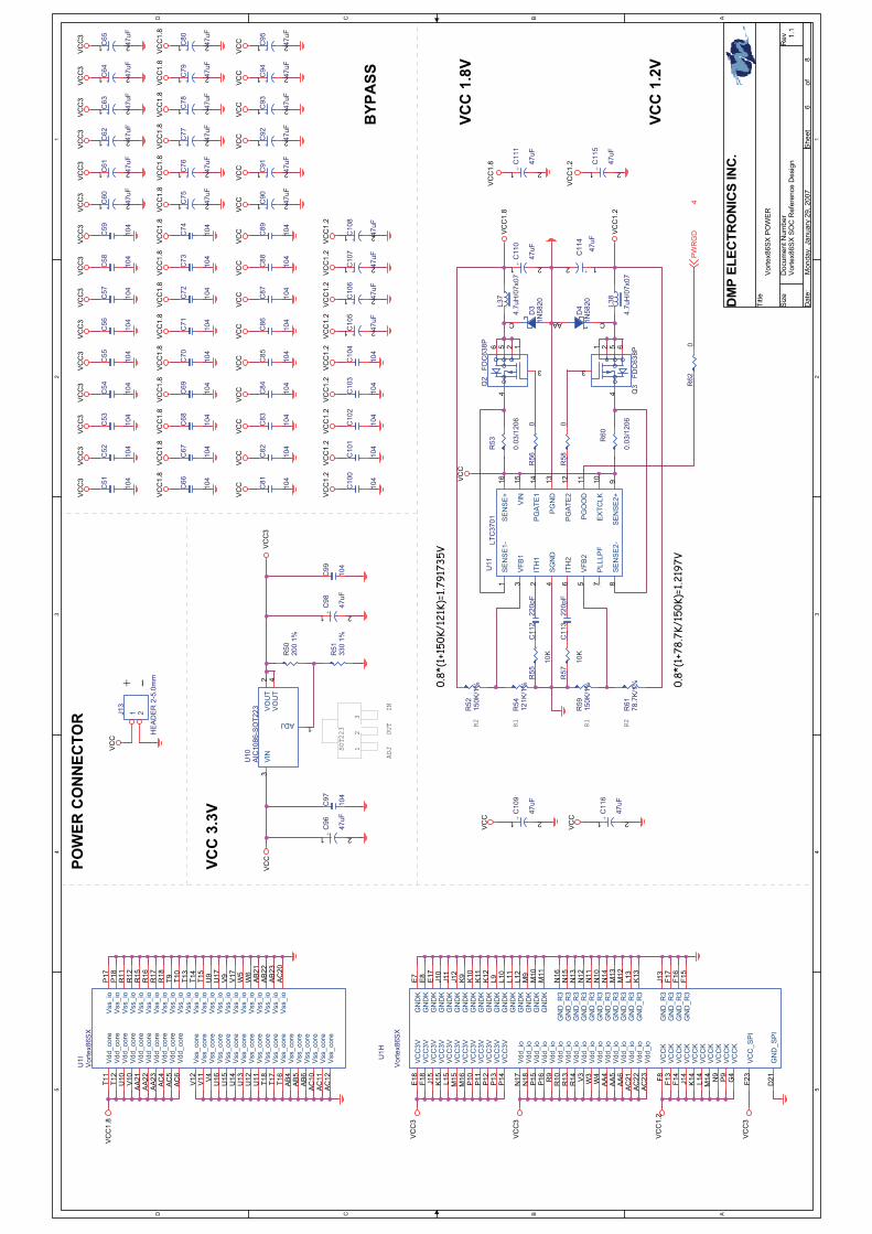
5 5
4 4
3 3
2 2
1 1
DD
CC
BB
AA
VCC
3.3
V
VCC
1.2
V
VCC
1.8
V
R1 R1 R2R2
0.8*
(1+150
K/12
1K)=1.7
9173
5V
0.8*
(1+7
8.7K
/150
K)=1.219
7V
2 OUT
13
SOT223
INADJ
+ -
POW
ER C
ON
NEC
TOR
BYP
ASS
Vor
tex8
6SX
SO
C R
efer
ence
Des
ign
1.1
Vor
tex8
6SX
PO
WE
R
DM
P EL
ECTR
ON
ICS
INC
.
68
Mon
day,
Jan
uary
29,
200
7
Title
Size
Doc
umen
t Num
ber
Rev
Dat
e:S
heet
of
PW
RG
D4
VC
C1.
8
VC
C3
VC
C3
VC
C1.
2
VC
C3
VC
C3
VC
C
VC
C
VC
C1.
8
VC
C1.
2
VC
C1.
8V
CC
VC
CV
CC
1.2
VC
C3
VC
C3
VC
C3
VC
C3
VC
C3
VC
C3
VC
C3
VC
C3
VC
C3
VC
C3
VC
C3
VC
C3
VC
C3
VC
C3
VC
C3
VC
C1.
8V
CC
1.8
VC
C1.
8V
CC
1.8
VC
C1.
8V
CC
1.8
VC
C1.
8V
CC
1.8
VC
C1.
8V
CC
1.8
VC
C1.
8V
CC
1.8
VC
C1.
8V
CC
1.8
VC
C1.
8
VC
CV
CC
VC
CV
CC
VC
CV
CC
VC
CV
CC
VC
CV
CC
VC
CV
CC
VC
CV
CC
VC
C
VC
C
VC
C1.
2V
CC
1.2
VC
C1.
2V
CC
1.2
VC
C1.
2V
CC
1.2
VC
C1.
2V
CC
1.2
VC
C1.
2
Q2
FDC
638P 2 1
4
3
6 5
C11
322
0pF
R53
0.03
/120
6
+
C98
47uF
1 2L3
8
4.7u
H/0
7x07
+
C96
47uF
1 2
C57
104
C53
104
C58
104
C54
104
C55
104
C59
104
C56
104
C52
104
C51
104
C10
1
104
C10
0
104
C10
4
104
C10
2
104
C10
3
104
C85
104
C86
104
C82
104
C83
104
C81
104
C87
104
C88
104
C84
104
C89
104
+C93
47uF
1 2
+C94
47uF
1 2
+C95
47uF
1 2
+C90
47uF
1 2
+C91
47uF
1 2
+C92
47uF
1 2
+C60
47uF
1 2
+C65
47uF
1 2
+C64
47uF
1 2
+C63
47uF
1 2
+C62
47uF
1 2
+C61
47uF
1 2
C68
104
C70
104
C74
104
C73
104
C66
104
C67
104
C72
104
C71
104
C69
104
+C76
47uF
1 2
+C77
47uF
1 2
+C80
47uF
1 2
+C75
47uF
1 2
+C78
47uF
1 2
+C79
47uF
1 2
+
C11
1
47uF
1 2
U1I
Vor
tex8
6SX
T11
T12
U10
V10
AA
21A
A22
AA
23A
C4
AC
5A
C6
T16
T17
T18
U11
U12
U13
U14
U15
U16V4
V11
V12
P17
P18
R11
R12
R15
R16
R17
R18
T9 T10
T13
T14
T15
U9
U17
V9
V17
W5
W6
AB
21A
B22
AB
23A
C20
AB
4A
B5
AB
6A
C10
AC
11A
C12
Vdd
_cor
eV
dd_c
ore
Vdd
_cor
eV
dd_c
ore
Vdd
_cor
eV
dd_c
ore
Vdd
_cor
eV
dd_c
ore
Vdd
_cor
eV
dd_c
ore
Vss
_cor
eV
ss_c
ore
Vss
_cor
eV
ss_c
ore
Vss
_cor
eV
ss_c
ore
Vss
_cor
eV
ss_c
ore
Vss
_cor
eV
ss_c
ore
Vss
_cor
eV
ss_c
ore
Vss
_io
Vss
_io
Vss
_io
Vss
_io
Vss
_io
Vss
_io
Vss
_io
Vss
_io
Vss
_io
Vss
_io
Vss
_io
Vss
_io
Vss
_io
Vss
_io
Vss
_io
Vss
_io
Vss
_io
Vss
_io
Vss
_io
Vss
_io
Vss
_io
Vss
_io
Vss
_io
Vss
_cor
eV
ss_c
ore
Vss
_cor
eV
ss_c
ore
Vss
_cor
eV
ss_c
ore
D3
1N58
20
AC
R50
200
1%
R52
150K
/1%
C99
104
R55
10K
C11
222
0pF
R56
0
R61
78.7
K/1
%
C97
104
R51
330
1%
+
C11
6
47uF
1 2
J13
HE
AD
ER
2-5
.0m
m
1 2
Q3
FDC
638P
21
4
3
65
R54
121K
/1%
+C10
8
47uF
1 2
+C10
5
47uF
1 2
+C10
7
47uF
1 2
+C10
6
47uF
1 2
+
C11
5
47uF
1 2
U1H
Vor
tex8
6SX
E18 F1
8J1
5K
15 L15
M15
M16
P10
N16
N15
N13
N12
N11
N10
N14
M13
M12
L13
K13
F8 F13
F14
J14
K14 L14
M14 N9
P9
G4
E7
E8
E17
J10
J11
J12
K9
K10
K11
K12
L9 L10
L11
L12
M9
M10
M11
P11
P12
P13
P14
J13
F17
F16
F15
F23
D21
N17
N18
P15
P16 R
9R
10R
13R
14 V3
W3
W4
AA
4A
A5
AA
6A
C21
AC
22A
C23
VC
C3V
VC
C3V
VC
C3V
VC
C3V
VC
C3V
VC
C3V
VC
C3V
VC
C3V
GN
D_R
3G
ND
_R3
GN
D_R
3G
ND
_R3
GN
D_R
3G
ND
_R3
GN
D_R
3G
ND
_R3
GN
D_R
3G
ND
_R3
GN
D_R
3
VC
CK
VC
CK
VC
CK
VC
CK
VC
CK
VC
CK
VC
CK
VC
CK
VC
CK
VC
CK
GN
DK
GN
DK
GN
DK
GN
DK
GN
DK
GN
DK
GN
DK
GN
DK
GN
DK
GN
DK
GN
DK
GN
DK
GN
DK
GN
DK
GN
DK
GN
DK
GN
DK
VC
C3V
VC
C3V
VC
C3V
VC
C3V
GN
D_R
3G
ND
_R3
GN
D_R
3G
ND
_R3
VC
C_S
PI
GN
D_S
PI
Vdd
_io
Vdd
_io
Vdd
_io
Vdd
_io
Vdd
_io
Vdd
_io
Vdd
_io
Vdd
_io
Vdd
_io
Vdd
_io
Vdd
_io
Vdd
_io
Vdd
_io
Vdd
_io
Vdd
_io
Vdd
_io
Vdd
_io
+
C11
0
47uF
1 2
R62
0
U10
AIC
1086
-SO
T223
3
1
2 4V
IN
ADJ
VO
UT
VO
UT
R58
0
U11
LTC
3701
1 23 4 56 7 8910111213141516
SE
NS
E1-
ITH
1
VFB
1
SG
ND
VFB
2
ITH
2
PLL
LPF
SE
NS
E2-
SE
NS
E2+
EX
TCLK
PG
OO
D
PG
ATE
2
PG
ND
PG
ATE
1
VIN
SE
NS
E+
+
C10
9
47uF
1 2
D4
1N58
20
A C
R59
150K
/1%
L37
4.7u
H/0
7x07
R60
0.03
/120
6
R57
10K
+
C11
4
47uF
12
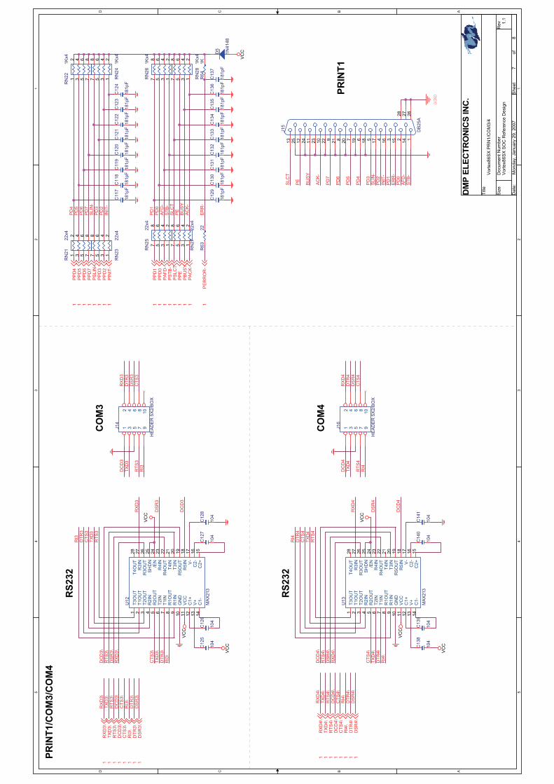
5 5
4 4
3 3
2 2
1 1
DD
CC
BB
AA
RS2
32
RS2
32
PRIN
T1
CO
M3
CO
M4
PRIN
T1/C
OM
3/C
OM
4
Vor
tex8
6SX
SO
C R
efer
ence
Des
ign
1.1
Vor
tex8
6SX
PR
N1/
CO
M3/
4
DM
P EL
ECTR
ON
ICS
INC
.
78
Mon
day,
Jan
uary
29,
200
7
Title
Size
Doc
umen
t Num
ber
Rev
Dat
e:S
heet
of
ER
R-
AC
K-
BU
SY
STB-
PE
STB-
AC
K-
INIT
-
PD
6
PD
3
BU
SY
PD
4
PD
1
PD
2
AFD
-
SLC
T
PD
7
ER
R-
PD
5
PD
0
PE
SLI
N-
RI3
\
DC
D3\
DTR
3\
DS
R3\
CTS
3
RX
D3
TXD
3\
DTR
3
RTS
3\
TXD
3
CTS
3\
RX
D3\
DC
D3
DS
R3
RI3
RTS
3
RX
D4
TXD
4\
RI4
\
CTS
4\D
SR
4
DC
D4
DTR
4\
CTS
4\
DTR
4\
DTR
3\R
I3\ DC
D4\
RTS
4\TX
D4\
RI4
\
CTS
3\
RX
D3\
DS
R3\
RTS
3\D
CD
3\
TXD
3\
RX
D4\
DS
R4\
PD
1P
D0
AFD
-
SLC
T
DC
D3
RX
D3
DTR
3D
SR
3R
TS3
CTS
3R
I3
TXD
3
DS
R4
RX
D4
CTS
4
DTR
4
RTS
4
TXD
4
RI4
DC
D4
PD
7P
D6
INIT
-P
D2
PD
5P
D4
SLI
N-
PD
3
DTR
4
RTS
4
RTS
4\
RX
D4\
RI4
CTS
4
DS
R4\
DC
D4\
TXD
4
PP
D4
1P
PD
51
PP
D6
1P
PD
71
PS
LCT
1P
PE
1P
BU
SY
1P
AC
K-
1
PIN
IT-
1
PE
RR
OR
-1
PA
FD-
1PS
TB-
1
DTR
4\1
RX
D4\
1
DS
R4\
1
DC
D4\
1
RI3
\1
TXD
3\1
CTS
3\1
DS
R3\
1
CTS
4\1
RTS
4\1
RX
D3\
1
RI4
\1
DTR
3\1
DC
D3\
1R
TS3\
1
TXD
4\1
PP
D1
1P
PD
01
PP
D2
1
PS
LIN
-1
PP
D3
1
GGND
VC
C
VC
C
VC
C
VC
C
VC
C
VC
C
VC
C
C13
7
181p
F
R64
1KR
N28
1Kx4
12
34
56
78
C12
6
104
C13
1
181p
F
C13
8
104
C13
4
181p
F
RN
261K
x4
12
34
56
78
C11
9
181p
FU
12
MAX
213
1 2 3 4 5 6 7 8 9 10 11 12 13 141516171819202122232425262728
T3O
UT
T1O
UT
T2O
UT
R2I
NR
2OU
TT2
INT1
INR
1OU
TR
1IN
GN
DV
CC
C1+
V+
C1-
C2+C2-V-
R5I
NR
5OU
TT3
INT4
INR
4OU
TR
4IN
/EN
SH
DN
R3O
UT
R3I
NT4
OU
T
RN
2322
x4
12
34
56
78
RN
241K
x4
12
34
56
78
C13
5
181p
F
C12
2
181p
F
RN
2522
x4
12
34
56
78
C14
0
104
J14
HE
AD
ER
5X
2/B
OX
12
34
56
78
910
C12
5
104
C13
0
181p
F
R63
22
J15
DB
25A
11421531641751861972082192210231124122513
262728
C13
2
181p
F
C13
6
181p
FD
5
1N41
48
C12
3
181p
F
C11
7
181p
F
RN
2722
x41
23
45
67
8
RN
2122
x41
23
45
67
8
C14
1
104
J16
HE
AD
ER
5X
2/B
OX
12
34
56
78
910
C12
0
181p
F
U13
MAX
213
1 2 3 4 5 6 7 8 9 10 11 12 13 141516171819202122232425262728
T3O
UT
T1O
UT
T2O
UT
R2I
NR
2OU
TT2
INT1
INR
1OU
TR
1IN
GN
DV
CC
C1+
V+
C1-
C2+C2-V-
R5I
NR
5OU
TT3
INT4
INR
4OU
TR
4IN
/EN
SH
DN
R3O
UT
R3I
NT4
OU
T
C11
8
181p
F
C12
7
104
C13
9
104
C12
8
104
C13
3
181p
F
C12
9
181p
F
RN
221K
x41
23
45
67
8
C12
4
181p
F
C12
1
181p
F
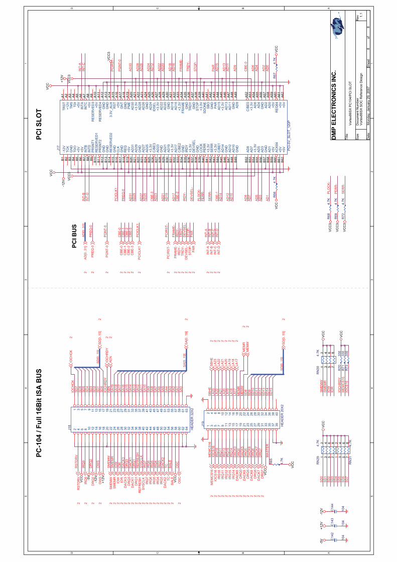
5 5
4 4
3 3
2 2
1 1
DD
CC
BB
AA
PC-1
04 /
Full
16B
it IS
A B
US
PCI B
US
PCI S
LOT
Vor
tex8
6SX
SO
C R
efer
ence
Des
ign
1.1
Vor
tex8
6SX
PC
104/
PC
I SLO
T
DM
P EL
ECTR
ON
ICS
INC
.
88
Mon
day,
Jan
uary
29,
200
7
Title
Size
Doc
umen
t Num
ber
Rev
Dat
e:S
heet
of
SA
[0..1
9]
IOC
HC
KS
D7
SD
6IR
Q9
SD
5S
D4
DR
Q2
SD
3S
D2
OW
SS
D1
SD
0IO
CH
RD
YSM
EMW
AE
NS
MEM
RS
A19
IOW
SA
18IO
RS
A17
DA
CK
3S
A16
DR
Q3
SA
15D
AC
K1
SA
14D
RQ
1S
A13
RE
FRE
SH
SA
12S
YS
CLK
SA
11IR
Q7
SA
10IR
Q6
SA
9IR
Q5
SA
8IR
Q4
SA
7IR
Q3
SA
6D
AC
K2
SA
5TC
SA
4B
ALE
SA
3S
A2
OS
CS
A1
SA
0
ME
MC
S16
SB
HE
IOC
S16
LA23
IRQ
10LA
22IR
Q11
LA21
IRQ
12IR
Q15
LA19
IRQ
14LA
18D
AC
K0
LA17
DR
Q0
MEM
RD
AC
K5
MEM
WD
RQ
5S
D8
DA
CK
6S
D9
DR
Q6
SD
10D
AC
K7
SD
11D
RQ
7S
D12
SD
13M
AST
ERS
D14
SD
15
LA20
SD
[0..1
5]
SD
[0..1
5]
RS
TDR
V
SD
0S
D1
SD
2S
D3
SD
6S
D7
SD
5S
D4
IOC
HR
DY
IOC
S16
ME
MC
S16
SM
EMR
SMEM
W
IOW
IOR
INT-
AIN
T-B
INT-
CIN
T-D
TRD
Y-
DE
VS
EL-
STO
P-P
AR
PC
IRS
T-
FRA
ME
-IR
DY
-
PC
ICLK
1
CB
E-0
CB
E-1
CB
E-2
CB
E-3
PG
NT-
0
PR
EQ
-0
AD
1
AD
7
AD
15
PE
RR
-
CB
E-3
PLO
CK
-
AD
11
AD
28
INT-
C
AD
17
AD
4
AD
29
AD
23
AD
20
AD
6
AD
10
CB
E-2
PC
ICLK
1
AD
8
AD
25
AD
2
INT-
B
FRA
ME
-
AD
19
IRD
Y-
AD
26A
D27
SE
RR
-
STO
P-
PG
NT-
0
AD
5
AD
14
PC
IRS
T-
TRD
Y-
AD
30
AD
24
INT-
D
AD
12
INT-
A
AD
16
AD
31
AD
3
DE
VS
EL-
AD
12
AD
18
AD
9
AD
13
PR
EQ
-0
AD
22A
D21
AD
0
PA
R
CB
E-0
CB
E-1 P
LOC
K-
SE
RR
-
PE
RR
-
AD
[0..3
1]R
STD
RV
2
IRQ
92
DA
CK
12
DR
Q1
2
SY
SC
LK2
IRQ
72
IRQ
52
IRQ
42
IRQ
32
TC2
BA
LE2
AE
N2
SA
[0..1
9]2
MEM
R2
MEM
W2
IRQ
102
IRQ
112
IRQ
122
IRQ
152
IRQ
142
DA
CK
52
DR
Q5
2
SD
[0..1
5]2
IOC
HR
DY
2
OW
S2
ME
MC
S16
2IO
CS
162
IOC
HC
K2
SB
HE
2
IOR
2IO
W2
SM
EMR
2SM
EMW
2
OS
C2
DA
CK
32
DR
Q3
2
IRQ
62
DA
CK
22
DR
Q2
2
DA
CK
02
DA
CK
62
DA
CK
72
DR
Q0
2
DR
Q6
2
DR
Q7
2
RE
FRE
SH
2
LA17
2LA
182
LA19
2LA
202
LA21
2LA
222
LA23
2
SD
[0..1
5]2
AD
[0..3
1]2
FRA
ME
-2
TRD
Y-
2
STO
P-2
CB
E-0
2C
BE
-12
CB
E-2
2C
BE
-32
PC
IRS
T-2
PG
NT-
02
PR
EQ
-02
PC
ICLK
12
IRD
Y-
2
PA
R2
DE
VS
EL-
2
INT-
B2
INT-
C2
INT-
D2
INT-
A2
VC
C
VC
C
-5V
-12V
VC
C
VC
C
VC
CV
CC
VC
C
VC
C3
+12V
-12V
VC
C3
VC
CV
CC
VC
CV
CC
VC
C3
VC
C3
VC
C3
VC
C3
+12V
-12V
+12V
-5V
R72
4.7K
J18
HE
AD
ER
32X
212
34
56
78
910
1112
1314
1516
1718
1920
2122
2324
2526
2728
2930
3132
3334
3536
3738
3940
4142
4344
4546
4748
4950
5152
5354
5556
5758
5960
61 6362 64
J19
HE
AD
ER
20X
2
12
34
56
78
910
1112
1314
1516
1718
1920
2122
2324
2526
2728
2930
3132
3334
3536
3738
3940
J17
PC
I-5V
_SLO
T_12
0P
A1
A2
A3
A4
A5
A6
A7
A8
A9
A10
A11
A12
A13
A14
A15
A16
A17
A18
A19
A20
A21
A22
A23
A24
A25
A26
A27
A28
A29
A30
A31
A32
A33
A34
A35
A36
A37
A38
A39
A40
A41
A42
A43
A44
A45
A46
A47
A48
A49
A52
A53
A54
A55
A56
A57
A58
A59
A60
A61
A62
B1
B2
B3
B4
B5
B6
B7
B8
B9
B10
B11
B12
B13
B14
B15
B16
B17
B18
B19
B20
B21
B22
B23
B24
B25
B26
B27
B28
B29
B30
B31
B32
B33
B34
B35
B36
B37
B38
B39
B40
B41
B42
B43
B44
B45
B46
B47
B48
B49
B52
B53
B54
B55
B56
B57
B58
B59
B60
B61
B62
TRS
T+1
2VTM
STD
I+5
VIN
TAIN
TC +5V
RE
SE
RV
ED
3+5
VR
ES
ER
VE
D4
GN
DG
ND
3.3V
_AU
XR
ST
+5V
GN
TG
ND
PM
EA
D30
+3.3
VA
D28
AD
26G
ND
AD
24ID
SE
L+3
.3V
AD
22A
D20
GN
DA
D18
AD
16+3
.3V
FRA
ME
GN
DTR
DY
GN
DS
TOP
+3.3
VS
DO
NE
SB
OG
ND
PA
RA
D15
+3.3
VA
D13
AD
11G
ND
AD
9
C/B
E0
+3.3
VA
D6
AD
4G
ND
AD
2A
D0
+5V
RE
Q64
+5V
+5V
-12V
TCK
GN
DTD
O+5
V+5
VIN
TBIN
TDP
RS
NT1
RE
SE
RV
ED
1P
RS
NT2
GN
DG
ND
RE
SE
RV
ED
2G
ND
CLK
GN
DR
EQ
+5V
AD
31A
D29
GN
DA
D27
AD
25+3
.3V
C/B
E3
AD
23G
ND
AD
21A
D19
+3.3
VA
D17
C/B
E2
GN
DIR
DY
+3.3
VD
EV
SE
LG
ND
LOC
KP
ER
R+3
.3V
SE
RR
+3.3
VC
/BE
1A
D14
GN
DA
D12
AD
10G
ND
AD
8A
D7
+3.3
VA
D5
AD
3G
ND
AD
1+5
VA
CK
64+5
V+5
V
R66
4.7K
R69
4.7K
R65
4.7K
R68
4.7K
R67
4.7K
RN
314.
7K
12
34
56
78
RN
294.
7K1
23
45
67
8
R70
330
C14
4
104
C14
2
104
C14
3
104
RN
304.
7K1
23
45
67
8
R71
330
R73
330