Volume 12 21 February 2021 Chemical Science
9
Chemical Science rsc.li/chemical-science Volume 12 Number 7 21 February 2021 Pages 2315–2684 ISSN 2041-6539 EDGE ARTICLE Eliseo Ruiz, Phimphaka Harding, David J. Harding, Christian A. Nijhuis et al. Room temperature conductance switching in a molecular iron(III ) spin crossover junction
Transcript of Volume 12 21 February 2021 Chemical Science

Chemical Sciencersc.li/chemical-science
Volume 12Number 721 February 2021Pages 2315–2684
ISSN 2041-6539
EDGE ARTICLEEliseo Ruiz, Phimphaka Harding, David J. Harding, Christian A. Nijhuis et al.Room temperature conductance switching in a molecular iron(III) spin crossover junction

ChemicalScience
EDGE ARTICLE
Ope
n A
cces
s A
rtic
le. P
ublis
hed
on 1
0 N
ovem
ber
2020
. Dow
nloa
ded
on 1
2/26
/202
1 4:
34:2
2 A
M.
Thi
s ar
ticle
is li
cens
ed u
nder
a C
reat
ive
Com
mon
s A
ttrib
utio
n-N
onC
omm
erci
al 3
.0 U
npor
ted
Lic
ence
.
View Article OnlineView Journal | View Issue
Room temperatu
aDepartment of Chemistry, National Uni
Singapore 117543, Singapore. E-mail: chmnbDepartament de Quımica Inorganica, Ins
Computacional, Universitat de Barcelona,
E-mail: [email protected] Materials and Nanotechnology C
Thasala, Nakhon Si Thammarat, 80160, Tha
[email protected] Synchrotron Light Source, Natio
Link, Singapore 117603, SingaporeeAustralian Synchrotron Clayton, Victoria 31fSchool of Chemistry and Physics, Queensl
Queensland 4001, AustraliagCentre for Advanced 2D Materials & Gra
Singapore, 6 Science Drive 2, Singapore 117
† Electronic supplementary information ((section S1, and Fig. S1), device characterithe temperature dependent XAS spectratheoretical analysis (section S2). See DOI:
Cite this: Chem. Sci., 2021, 12, 2381
All publication charges for this articlehave been paid for by the Royal Societyof Chemistry
Received 19th August 2020Accepted 9th November 2020
DOI: 10.1039/d0sc04555a
rsc.li/chemical-science
© 2021 The Author(s). Published by
re conductance switching ina molecular iron(III) spin crossover junction†
Senthil Kumar Karuppannan, a Alejandro Martın-Rodrıguez,b Eliseo Ruiz,*b
Phimphaka Harding, *c David J. Harding, *c Xiaojiang Yu,d Anton Tadich,e
Bruce Cowie,f Dongchen Qif and Christian A. Nijhuis *ag
Herein, we report the first room temperature switchable Fe(III) molecular spin crossover (SCO) tunnel
junction. The junction is constructed from [FeIII(qsal-I)2]NTf2 (qsal-I ¼ 4-iodo-2-[(8-quinolylimino)
methyl]phenolate) molecules self-assembled on graphene surfaces with conductance switching of one
order of magnitude associated with the high and low spin states of the SCO complex. Normalized
conductance analysis of the current–voltage characteristics as a function of temperature reveals that
charge transport across the SCO molecule is dominated by coherent tunnelling. Temperature-
dependent X-ray absorption spectroscopy and density functional theory confirm the SCO complex
retains its SCO functionality on the surface implying that van der Waals molecule—electrode interfaces
provide a good trade-off between junction stability while retaining SCO switching capability. These
results provide new insights and may aid in the design of other types of molecular devices based on SCO
compounds.
Introduction
Spin crossover (SCO) molecules are promising candidates in thedevelopment of various spintronic and data storage devices asthey can switch between two electronic states, dened by theirhigh spin (HS) and low spin (LS) states.1–3 Given that switchingcan be triggered by various external stimuli, such as, tempera-ture, pressure, light, or adsorption of guest molecules, SCOmolecules also nd applications as smart materials thatrespond to several stimuli. Devices based on thin lms4–7 (witha thickness of typically 10–100 nm) of SCO molecules exhibit
versity of Singapore, 3 Science Drive,
titut de Recerca de Quımica Teorica i
Diagonal 645, 08028 Barcelona, Spain.
enter of Excellence, Walailak University,
iland. E-mail: [email protected];
nal University of Singapore, 5 Research
68, Australia
and University of Technology, Brisbane,
phene Research, National University of
546, Singapore
ESI) available: The XPS characterizationstics of various SCO junction (Table S1),of powder SCO sample, and detailed10.1039/d0sc04555a
the Royal Society of Chemistry
spin-polarized current switching,8 voltage-bias,9 and stretch-ing10 induced resistance switching, and memristive proper-ties,11 but it is still challenging, however, to incorporate SCOmolecules in molecular tunnel junctions as they are prone todecomposition, or conformational distortion, such that theylose their SCO properties.4,5,8 In addition, the molecule–elec-trode coupling has to be optimized because too strong mole-cule–electrode coupling leads to drastic alteration of theirmagnetic properties, even a complete loss of SCO behaviour,12–14
yet too weak coupling compromises stability of the devices.11,15 Asummary of these different parameters for the SCO molecule-based junctions is given in Table S1.† Here we report a molec-ular tunnel junction with a monolayer (unlike the morecommon multi-layers) of FeIII SCO molecules adsorbed via self-assembly on single-layer graphene on Cu and with EGaIn top-contacts that can be switched between HS and LS states ata remarkably high-temperature T ¼ 310 K resulting in a 10-foldchange in the conductivity of the junction. Importantly, bothelectrodes form van der Waals contacts with the SCO moleculesensuring an optimal trade-off between junction stability andcoupling strength so that the SCO properties are retained incontrast to other approaches that rely on covalent or electro-static interactions and in which the interface chemistry is oennot controlled. Spectroscopy and DFT calculations show that,unlike other systems, the FeIII state is preserved illustrating thepotential of FeIII SCO materials as a new class of switchablemolecular materials.
As noted above overly strong molecule—electrode couplinginteractions can result in the adsorption of mixtures of HS and
Chem. Sci., 2021, 12, 2381–2388 | 2381

Fig. 1 (A) Schematic illustration of the SCO molecule based devicewith the EGaIn top-electrode stabilized in a small through-hole ina rubber stamp (made of PDMS) and (B) the SCO based molecularjunction of the form of Cu//SLG//[FeIII(qsal-I)2]NTf2//GaOx/EGaIn(EGaIn ¼ eutectic alloy of Ga and In).
Chemical Science Edge Article
Ope
n A
cces
s A
rtic
le. P
ublis
hed
on 1
0 N
ovem
ber
2020
. Dow
nloa
ded
on 1
2/26
/202
1 4:
34:2
2 A
M.
Thi
s ar
ticle
is li
cens
ed u
nder
a C
reat
ive
Com
mon
s A
ttrib
utio
n-N
onC
omm
erci
al 3
.0 U
npor
ted
Lic
ence
.View Article Online
LS molecules. Consequently, the relative population of the twospin states cannot be changed by external stimuli.11,13,15 Forexample, thin lms of [Fe(NCS)2(phen)2] on Cu(100) traps themolecules in either the HS or LS state, but adding a CuN layerdecouples the SCO molecules from the substrate allowing themto be electrically switched.15 To reduce the electrode—moleculecoupling strength, highly oriented pyrolytic graphite (HOPG)has been used as a substrate onto which SCOs form non-covalent monolayers.16–19 This strategy resulted in thermallyand light-activated SCO monolayers17,18 likely because the vander Waals interactions between SCO molecules and HOPG areweaker than between SCO molecules and bare metals.
While the above thin lms show promise, molecular SCOdevices are still rare. Using break junctions, [Fe(bpp-py)2]
2+
(bpp-py ¼ 2,6-(bis(pyrazol-1-yl)-4-pyridyl)pyridine)20 and [Fe(tpy-R)(tpy-R0)]2+ (tpy-R ¼ substituted terpyridine)21 showed voltage-induced switching of the spin sate. Van der Zant and co-workersshowed that [Fe(tpy-C6H4-S)2] placed between two gold elec-trodes can be stretched to induce a change in the spin state andconductance.21 An inherent challenge with break junctions isthe high failure rate and difficulty in achieving consistentorientation of the molecules in the junction. Recently,[Fe(HB(tz)3)2] molecules have been incorporated in large-areajunctions1–4,22 in the form of thin lms (6–100 nm thick), butdepending on the fabrication methods either conductanceswitching was associated with a LS / HS transition,7 or HS /
LS4,5 highlighting the challenges in controlling the character-istics of the device.
Despite these successes, comparatively few systems havebeen used in molecular junctions, almost all of them are FeII
SCOs, and in many cases, the switching occurs only at very lowtemperatures.11,23–25 By comparison, despite their greaterrobustness, FeIII SCO complexes are almost entirely absent inSCO molecular junctions. The rst report involved subliming[Fe(pap)2]ClO4 (pap ¼ N-2-pyridylmethylidene-2-hydroxyphenylaminato) onto Au(111), but only a small propor-tion of the molecules were switchable.11 Use of Cu2N islands onthe Au(111) surface decouples the SCO molecules from the Auand allowed for more efficient electrical switching using an STMtip at low T ¼ 4.5 K.24 Nevertheless, the harshness of thedeposition technique risks changing the oxidation state of theiron centre and it was not conrmed that the SCO moleculesremain in the FeIII state on the surface.
To address these challenges to obtain robust molecular SCOjunctions, we selected [FeIII(qsal-I)2]NTf2 (qsal-I ¼ 4-iodo-2-[(8-quinolylimino)methyl]phenolate) as it exhibits a stronglyhysteretic spin transition at room temperature.26 We haveshown before that single-layer graphene (SLG) on Cu (Cu//SLGwhere “//” denotes a van der Waals interface) is an excellentplatform to form stable monolayers of functional molecules dueto favorable van der Waals interactions27 yet without chargetransfer between the molecules and the surface ensuring themolecular frontier orbitals remain localized on the molecules;28
we have used this approach to make efficient molecular diodes.Here we report that Cu//SLG//[FeIII(qsal-I)2]NTf2//GaOx/EGaInjunctions (the EGaIn top-electrode also forms a van der Waalscontact with the monolayer, Fig. 1) show clear spin-state
2382 | Chem. Sci., 2021, 12, 2381–2388
switching, leading to one order of magnitude change inconductance. These results are supported by extensive theo-retical modeling and represent the rst example of a roomtemperature switchable FeIII SCO molecular junction.
Results and discussionCharacterization of the Cu//SLG//[FeIII(qsal-I)2]NTf2
The device architecture is illustrated in Fig. 1. Briey, graphenewas grown on Cu foil using the chemical vapour depositionmethod, as described elsewhere.29 The synthesis of [FeIII(qsal-I)2]NTf2 has been reported elsewhere.26 We physisorbed[FeIII(qsal-I)2]NTf2 onto the SLG by immersing the CU//SLGsubstrate in a 1.0 mM solution of [FeIII(qsal-I)2]NTf2 inCH2Cl2. We formed junctions by contacting a monolayer ofphysisorbed [FeIII(qsal-I)2]NTf2 with GaOx/EGaIn to-electrodes(EGaIn stands for eutectic gallium–indium; 75.5% Ga and24.5% In by weight). Here, the EGaIn was stabilized ina through-hole in polydimethylsiloxane (PDMS) and the fabri-cation of this top contact has been reported elsewhere.30
We used Raman spectroscopy to determine the quality of thegraphene31 and to obtain additional information regarding thegraphene–molecule interactions. The important features in theRaman spectra of graphene are the sharp peak at �1587 cm�1
which corresponds to the rst order Raman scattering processin graphene (called the G band) and the second order peakinvolving two phonons at 2678 cm�1 is associated with twophonons (called a 2D band). In the case of disordered graphene,we can also observe another second order peak at about half ofthe frequency of the 2D band (�1200 cm�1), which is called thedisorder-induced D-band involving one phonon and one defect.The relative intensity of the D-band is directly proportional tothe level of defects in the sample.31 Fig. 2A shows the Ramanspectrum of our pristine Cu//SLG sample. The intensity ratio of
© 2021 The Author(s). Published by the Royal Society of Chemistry
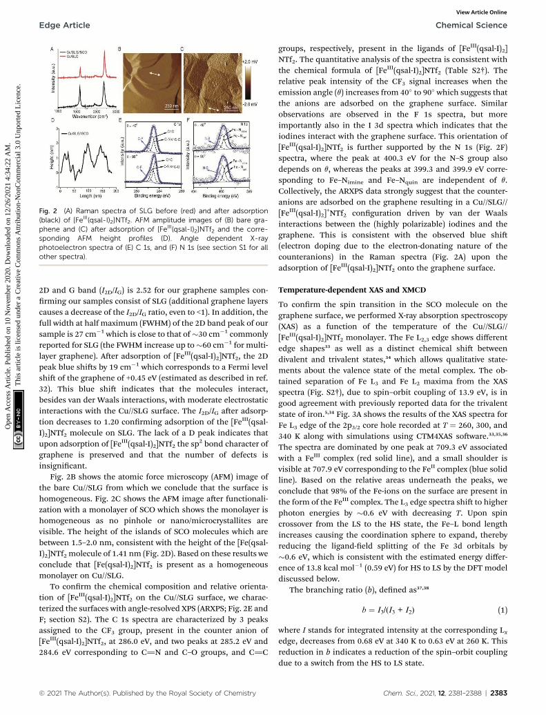
Fig. 2 (A) Raman spectra of SLG before (red) and after adsorption(black) of [FeIII(qsal-I)2]NTf2. AFM amplitude images of (B) bare gra-phene and (C) after adsorption of [FeIII(qsal-I)2]NTf2 and the corre-sponding AFM height profiles (D). Angle dependent X-rayphotoelectron spectra of (E) C 1s, and (F) N 1s (see section S1 for allother spectra).
Edge Article Chemical Science
Ope
n A
cces
s A
rtic
le. P
ublis
hed
on 1
0 N
ovem
ber
2020
. Dow
nloa
ded
on 1
2/26
/202
1 4:
34:2
2 A
M.
Thi
s ar
ticle
is li
cens
ed u
nder
a C
reat
ive
Com
mon
s A
ttrib
utio
n-N
onC
omm
erci
al 3
.0 U
npor
ted
Lic
ence
.View Article Online
2D and G band (I2D/IG) is 2.52 for our graphene samples con-rming our samples consist of SLG (additional graphene layerscauses a decrease of the I2D/IG ratio, even to <1). In addition, thefull width at half maximum (FWHM) of the 2D band peak of oursample is 27 cm�1 which is close to that of�30 cm�1 commonlyreported for SLG (the FWHM increase up to�60 cm�1 for multi-layer graphene). Aer adsorption of [FeIII(qsal-I)2]NTf2, the 2Dpeak blue shis by 19 cm�1 which corresponds to a Fermi levelshi of the graphene of +0.45 eV (estimated as described in ref.32). This blue shi indicates that the molecules interact,besides van der Waals interactions, with moderate electrostaticinteractions with the Cu//SLG surface. The I2D/IG aer adsorp-tion decreases to 1.20 conrming adsorption of the [FeIII(qsal-I)2]NTf2 molecule on SLG. The lack of a D peak indicates thatupon adsorption of [FeIII(qsal-I)2]NTf2 the sp
2 bond character ofgraphene is preserved and that the number of defects isinsignicant.
Fig. 2B shows the atomic force microscopy (AFM) image ofthe bare Cu//SLG from which we conclude that the surface ishomogeneous. Fig. 2C shows the AFM image aer functionali-zation with a monolayer of SCO which shows the monolayer ishomogeneous as no pinhole or nano/microcrystallites arevisible. The height of the islands of SCO molecules which arebetween 1.5–2.0 nm, consistent with the height of the [Fe(qsal-I)2]NTf2 molecule of 1.41 nm (Fig. 2D). Based on these results weconclude that [Fe(qsal-I)2]NTf2 is present as a homogeneousmonolayer on Cu//SLG.
To conrm the chemical composition and relative orienta-tion of [FeIII(qsal-I)2]NTf2 on the Cu//SLG surface, we charac-terized the surfaces with angle-resolved XPS (ARXPS; Fig. 2E andF; section S2). The C 1s spectra are characterized by 3 peaksassigned to the CF3 group, present in the counter anion of[FeIII(qsal-I)2]NTf2, at 286.0 eV, and two peaks at 285.2 eV and284.6 eV corresponding to C]N and C–O groups, and C]C
© 2021 The Author(s). Published by the Royal Society of Chemistry
groups, respectively, present in the ligands of [FeIII(qsal-I)2]NTf2. The quantitative analysis of the spectra is consistent withthe chemical formula of [FeIII(qsal-I)2]NTf2 (Table S2†). Therelative peak intensity of the CF3 signal increases when theemission angle (q) increases from 40� to 90� which suggests thatthe anions are adsorbed on the graphene surface. Similarobservations are observed in the F 1s spectra, but moreimportantly also in the I 3d spectra which indicates that theiodines interact with the graphene surface. This orientation of[FeIII(qsal-I)2]NTf2 is further supported by the N 1s (Fig. 2F)spectra, where the peak at 400.3 eV for the N–S group alsodepends on q, whereas the peaks at 399.3 and 399.9 eV corre-sponding to Fe–Nimine and Fe–Nquin are independent of q.Collectively, the ARXPS data strongly suggest that the counter-anions are adsorbed on the graphene resulting in a Cu//SLG//[FeIII(qsal-I)2]
+NTf2 conguration driven by van der Waalsinteractions between the (highly polarizable) iodines and thegraphene. This is consistent with the observed blue shi(electron doping due to the electron-donating nature of thecounteranions) in the Raman spectra (Fig. 2A) upon theadsorption of [FeIII(qsal-I)2]NTf2 onto the graphene surface.
Temperature-dependent XAS and XMCD
To conrm the spin transition in the SCO molecule on thegraphene surface, we performed X-ray absorption spectroscopy(XAS) as a function of the temperature of the Cu//SLG//[FeIII(qsal-I)2]NTf2 monolayer. The Fe L2,3 edge shows differentedge shapes33 as well as a distinct chemical shi betweendivalent and trivalent states,34 which allows qualitative state-ments about the valence state of the metal complex. The ob-tained separation of Fe L3 and Fe L2 maxima from the XASspectra (Fig. S2†), due to spin–orbit coupling of 13.9 eV, is ingood agreement with previously reported data for the trivalentstate of iron.5,34 Fig. 3A shows the results of the XAS spectra forFe L3 edge of the 2p3/2 core hole recorded at T ¼ 260, 300, and340 K along with simulations using CTM4XAS soware.33,35,36
The spectra are dominated by one peak at 709.3 eV associatedwith a FeIII complex (red solid line), and a small shoulder isvisible at 707.9 eV corresponding to the FeII complex (blue solidline). Based on the relative areas underneath the peaks, weconclude that 98% of the Fe-ions on the surface are present inthe form of the FeIII complex. The L3 edge spectra shi to higherphoton energies by �0.6 eV with decreasing T. Upon spincrossover from the LS to the HS state, the Fe–L bond lengthincreases causing the coordination sphere to expand, therebyreducing the ligand-eld splitting of the Fe 3d orbitals by�0.6 eV, which is consistent with the estimated energy differ-ence of 13.8 kcal mol�1 (0.59 eV) for HS to LS by the DFT modeldiscussed below.
The branching ratio (b), dened as37,38
b ¼ I3/(I3 + I2) (1)
where I stands for integrated intensity at the corresponding Lxedge, decreases from 0.68 eV at 340 K to 0.63 eV at 260 K. Thisreduction in b indicates a reduction of the spin–orbit couplingdue to a switch from the HS to LS state.
Chem. Sci., 2021, 12, 2381–2388 | 2383

Fig. 3 (A) The X-ray absorption spectra (XAS) of the Fe L3 edge fora monolayer of [FeIII(qsal-I)2]NTf2 on graphene at different tempera-tures, along with simulated peaks for octahedral (Oh) Fe
2+ and Fe3+
ions obtained with the CTM4XAS program. The XAS spectra of Fe L3edges for two different external magnetic field directions at (B) 340 K,(C) 300 K, and (D) 260 K. The difference between the XAS signalsobserved at +1.5 T and �1.5 T defines the XMCD signal.
Fig. 4 (A) Heatmap of log│J│ vs. (V) curves, the solid black line is thehlog10|J|iG vs. V curve. (B) J(V) curves recorded as a function oftemperature 340 / 240 / 340 K at intervals of 10 K for Cu//SLG//[FeIII(qsal-I)2]NTf2//GaOx/EGaIn junction. (C) J as a function oftemperature at �1.0 V applied bias (solid lines are visual guides), and(D) normalized differential conductance for the Cu//SLG//[FeIII(qsal-I)2]NTf2//GaOx/EGaIn junction at different temperature; solid lines arefits to the eqn (2).
Chemical Science Edge Article
Ope
n A
cces
s A
rtic
le. P
ublis
hed
on 1
0 N
ovem
ber
2020
. Dow
nloa
ded
on 1
2/26
/202
1 4:
34:2
2 A
M.
Thi
s ar
ticle
is li
cens
ed u
nder
a C
reat
ive
Com
mon
s A
ttrib
utio
n-N
onC
omm
erci
al 3
.0 U
npor
ted
Lic
ence
.View Article Online
We performed temperature-dependent XAS measurements ofour SCO compound in powder form to conrm whether theswitching characteristics of the SCO molecule on graphene aresimilar to that of the powder form. Fig. S3† shows the Fe L2,3 edgespectra with spin–orbit coupling energy of 13.4 eV which conrmsthe presence of FeIII in the SCO complex. Both L2 (720 eV) and L3(707 eV) edges shi to higher binding energy with decreasingtemperature from 340 K to 120 K, which conrms the HS to LStransition of the molecule occurs at lower temperature in thepowder form (see Fig. S3B† for T dependent magnetic hysteresisloop) as compared to that of themolecule on the graphene surfacein agreement with a previously reported transition of the SCOmolecule in powder form where the transition temperature T1/2for cooling is 248 K and T1/2 for heating is 278 K.26,39
To further conrm the spin transition of the monolayers ongraphene, we recorded the X-ray magnetic circular dichroism(XMCD) spectra in total electron yield mode with a magneticeld applied to the sample, which is parallel to the circularlypolarized photoelectron propagation vector. All the spectra arereported with a magnetic eld of �1.5 T at different tempera-tures. Fig. 3B–D show the results for the Fe L3 edge and that theHS complex shows a higher XMCD signal than the LS complex.40
The observed negative XMCD signal (Fig. 3B) at a photon energyof 710.3 eV indicates the presence of spin-polarized FeIII withoctahedral symmetry.36,41 Fig. 3D shows only a weak negativeXMCD signal at 710 eV at 260 K which indicates that the SCOcomplex switches from HS (S ¼ 5/2) to LS (S ¼ 1/2) (see DFTcalculations below) since the LS state has a smaller number ofuncompensated spins than the HS state. It is important to notethat, we only have a monolayer of the SCO complex adsorbed on
2384 | Chem. Sci., 2021, 12, 2381–2388
the surface, and consequently, the signal is very small whichprevents us to quantitatively t to the spectra.15 These resultsare consistent with the magnetic susceptibility measurement ofthe SCO molecule in powder form reported before showing anabrupt SCO transition with noticeable hysteresis.26 Thus, theobserved results lead to the utilization of the spin-stateconductance switching on the graphene surface for the inde-pendent switchability of the magnetic molecules in magnetictunnel junctions at room temperature.
Charge transport measurements
To investigate how the tunnelling characteristics of the junc-tions change with T, we determined the electrical propertieswith a statistically large number of J(V) curves to allow us toselect devices which had their characteristics within one log-standard deviation for temperature dependent measurementsusing well-established methods.42–44 We fabricated 50 Cu//SLG//[FeIII(qsal-I)2]NTf2//GaOx/EGaIn junctions with cone-shapedtips of EGaIn using 8 different substrates with a yield of non-shoring junctions of 88%. Fig. 4A shows the heatmap of allJ(V) curves (1150 in total) along with the Gaussian log-averagecurrent densities, hlog10|J|iG, (solid black line). The log-standard deviations, slog,G, fall in the range of 0.4 to 0.8which are comparable to other highly reproducible EGaInjunctions.29,30,45–48 Given the high yields and small spread in thedata we conclude the formation of Cu//SLG//[FeIII(qsal-I)2]NTf2//EGaIn junctions is highly reproducible. None of the junctionsshorted during 25 consecutive J(V) sweeps from which weconclude that the junctions are stable.
We measured the J(V) curves of Cu//SLG//[FeIII(qsal-I)2]NTf2//GaOx/EGaIn junctions as a function of temperature (T ¼ 240–
© 2021 The Author(s). Published by the Royal Society of Chemistry

Edge Article Chemical Science
Ope
n A
cces
s A
rtic
le. P
ublis
hed
on 1
0 N
ovem
ber
2020
. Dow
nloa
ded
on 1
2/26
/202
1 4:
34:2
2 A
M.
Thi
s ar
ticle
is li
cens
ed u
nder
a C
reat
ive
Com
mon
s A
ttrib
utio
n-N
onC
omm
erci
al 3
.0 U
npor
ted
Lic
ence
.View Article Online
340 K) using EGaIn stabilized in a through-hole in a micro-uidic network in PDMS (polydimethylsiloxane) followinga previously reported method30 (section S3). Fig. 4B shows theJ(V) characteristics recorded while cooling and subsequentheating of the junction (Fig. S4 and S5† show another 2 sets ofdata). Fig. 4C shows the corresponding evolution of the valuesof J at�1.0 and +1.0 V. The observed difference in the width andthe position of the hysteresis under positive and negative biaspolarity is most likely due to small conformational differencesof the SCO complex similar to observations made by Miyamachiet al.15 and Poggini et al.4 Moreover, from these data we makethe following 3 observations. (1) The value of J changes by oneorder of magnitude with T. This large switch in the observedcurrent proves that FeIII complexes can perform similarly well asFeII complexes and the transition from HS / LS does notpreclude efficient current switching in molecular junctions. Inthe case of Fe(II) complexes the two spin states HS and LS areparamagnetic and diamagnetic, respectively. It has been sug-gested that as both spin states are paramagnetic in the case ofFe(III), the magnitude of the change in current upon SCO wouldbe less for Fe(III) compared to Fe(II).5,15 Our results show that thisis not necessarily true. (2) The SCO transition occurs aroundroom temperature from 300 to 330 K. This switching tempera-ture is consistent with the XAS and XMCD results discussedabove. (3) The SCO transition of [FeIII(qsal-I)2]NTf2 in thejunction is more gradual with the average transition tempera-ture T1/2 (the temperature at which 50% HS to LS conversion)shied from 263 (for [FeIII(qsal-I)2]NTf2 in the powder form) toca. 300 K. As our original report showed,26 andmore recent workconrms, the hysteresis in [FeIII(qsal-I)2]NTf2 is intimatelyassociated with a conformational change in the NTf2 anion.49
The adsorption of the NTf2 anions on the SLG surface likelyprevents such conformational change and the presence of onlya single layer of [FeIII(qsal-I)2]
+ cations will further reducecooperativity leading to an increase in the spin transitiontemperature and a loss of hysteresis in the junction.49 It isnoteworthy that in the [Fe(HB(trz)3)2] system, which alsoincorporates an EGaIn top-electrode, a small shi in T1/2 tohigher temperature is observed.5 Moreover, a very recent reportwith an Fe(III) compound shows a shi from 80 K (bulk) to 200 K(junction).50 These results show that the Cu//SLG is a promisingplatform to anchor SCO molecules in a stable manner withoutcompromising their SCO behaviour.
Recently, the SCO behaviour of Au//[FeII(HB(trz)3)2]//Ga2O3/EGaIn junctions with 6.7 nm thick lms (�7 molecular layers)directly adsorbed on Au was reported. Here, an anomalous SCOtransition was observed within 1 K for which no explanation wasgiven.5 In a follow up study, a very broad SCO transition from100–300 K was reported for Au//[Fe(H2B(pz)2)2(phen)]//GaOx/EGaIn junctions with 5.6 nm thick molecular lms. The authorsproposed a switch in the mechanism of charge transport fromcoherent tunnelling in the LS state to incoherent tunnelling (orhopping) in the HS state. However, a plateau of the current stateat high T was not observed and Arrhenius plots of the low orhigh conductance states were not reported, hampering eluci-dation of the mechanism of charge transport experimentally.4
© 2021 The Author(s). Published by the Royal Society of Chemistry
In general, to establish the mechanism of charge transport itis important to perform J(V) measurements as a function ofT.5,48,51,52 Coherent tunnelling is independent of the T, and theJ(V) curve is parabolic in nature.51,52 In contrast, incoherenttunnelling (or hopping) is thermally activated where chargeshop to available molecule energy states causing deviations fromparabolic behaviour,53 and strongly depends on the T andweakly dependents on the tunneling distance. However, toelucidate the mechanism of charge transport across the Cu//SLG//[FeIII(qsal-I)2]NTf2//GaOx/EGaIn junctions in the high andlow conduction states, we performed normalized differentialconductance (NDC) analysis using eqn (2), as describedbefore,51,52 to determine whether the J(V) curves are parabolic.
NDC ¼ dJ
dV:V
J¼ dðlog JÞ
dðlog VÞ (2)
For the NDC analysis we used the individual J(V) traces ob-tained at 340 and 250 K. Fig. 4D shows the NDC curves showtypical parabolic behaviour approaching NDC ¼ 3 at �1.0 Vcharacteristic for coherent tunnelling. The NDC plots showa small asymmetry which is likely due to the different top andbottom electrode materials. The calculations below show thatmolecular orbitals are available (i.e., have their energies close tothe energy of the Fermi level, EF) for charge transport whichexplains the relatively high tunnelling currents (10–100 timeshigher than for junctions with conjugated molecules of similarlength that are dominated by off resonant tunnelling54–56).Therefore, we conclude that the dominant mechanism ofcharge transport is resonant coherent tunnelling.
Theoretical modelling of the junction
We modelled the complex structure of the EGaIn electrode bystarting with the X-ray structure of a-gallium57 [100] onto whicha monolayer of O2 molecules was placed. We added randomlypositioned Ga and In atoms following the experimental stoi-chiometric ratio of EGaIn (the eutectic is composed of 75.5% Gaand 24.5 Ga% In by weight) to obtain the fully optimized topelectrode. Different binding conformations of [FeIII(qsal-I)2]NTf2 with SLG were considered (see section S2), but theconformation with the two iodine atoms interacting with gra-phene is the most stable one (see Fig. 5), which is consistentwith the XPS result discussed earlier. We hypothesize thata combination of anion/p and I/p interactions aid non-covalent attachment of [FeIII(qsal-I)2]NTf2 to the graphenesurface. Finally, the complete junction including the Cu//SLGbottom electrode was fully optimized for the high- and low-spin states of the metal complex (the cif les of the optimizedstructures can be found in the ESI, Fig. S6†).
The relative stability of the two states of the metal complexwas computed using the non-hybridmeta-GGA SCAN functional,which indicates that the S ¼ 1/2 low-spin state is the groundstate, which is 28.0 kcal mol�1 (1.21 eV) more stable than the S¼5/2 high-spin state, which is consistent with the observed shi(1.66 eV) in the XAS spectra of the powder form of [FeIII(qsal-I)2]NTf2 (Fig. S3†).26 Here we report that the stabilization of the HS
Chem. Sci., 2021, 12, 2381–2388 | 2385
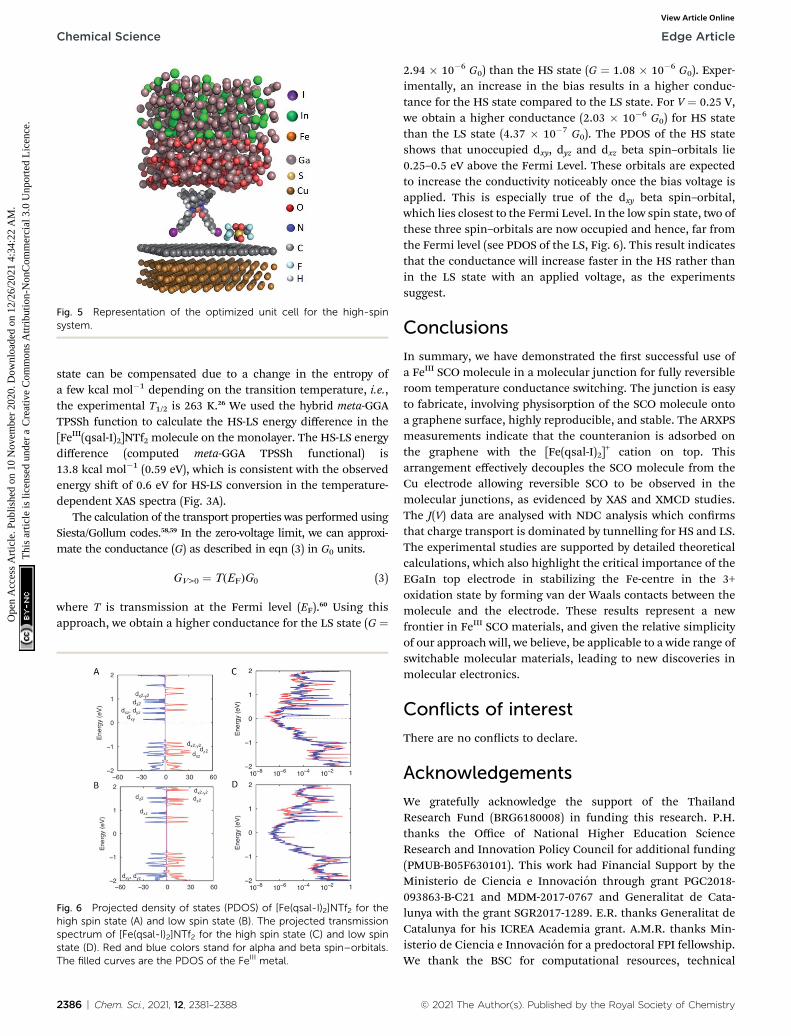
Fig. 5 Representation of the optimized unit cell for the high-spinsystem.
Chemical Science Edge Article
Ope
n A
cces
s A
rtic
le. P
ublis
hed
on 1
0 N
ovem
ber
2020
. Dow
nloa
ded
on 1
2/26
/202
1 4:
34:2
2 A
M.
Thi
s ar
ticle
is li
cens
ed u
nder
a C
reat
ive
Com
mon
s A
ttrib
utio
n-N
onC
omm
erci
al 3
.0 U
npor
ted
Lic
ence
.View Article Online
state can be compensated due to a change in the entropy ofa few kcal mol�1 depending on the transition temperature, i.e.,the experimental T1/2 is 263 K.26 We used the hybrid meta-GGATPSSh function to calculate the HS-LS energy difference in the[FeIII(qsal-I)2]NTf2 molecule on the monolayer. The HS-LS energydifference (computed meta-GGA TPSSh functional) is13.8 kcal mol�1 (0.59 eV), which is consistent with the observedenergy shi of 0.6 eV for HS-LS conversion in the temperature-dependent XAS spectra (Fig. 3A).
The calculation of the transport properties was performed usingSiesta/Gollum codes.58,59 In the zero-voltage limit, we can approxi-mate the conductance (G) as described in eqn (3) in G0 units.
GV>0 ¼ T(EF)G0 (3)
where T is transmission at the Fermi level (EF).60 Using thisapproach, we obtain a higher conductance for the LS state (G ¼
Fig. 6 Projected density of states (PDOS) of [Fe(qsal-I)2]NTf2 for thehigh spin state (A) and low spin state (B). The projected transmissionspectrum of [Fe(qsal-I)2]NTf2 for the high spin state (C) and low spinstate (D). Red and blue colors stand for alpha and beta spin–orbitals.The filled curves are the PDOS of the FeIII metal.
2386 | Chem. Sci., 2021, 12, 2381–2388
2.94 � 10�6 G0) than the HS state (G ¼ 1.08 � 10�6 G0). Exper-imentally, an increase in the bias results in a higher conduc-tance for the HS state compared to the LS state. For V ¼ 0.25 V,we obtain a higher conductance (2.03 � 10�6 G0) for HS statethan the LS state (4.37 � 10�7 G0). The PDOS of the HS stateshows that unoccupied dxy, dyz and dxz beta spin–orbitals lie0.25–0.5 eV above the Fermi Level. These orbitals are expectedto increase the conductivity noticeably once the bias voltage isapplied. This is especially true of the dxy beta spin–orbital,which lies closest to the Fermi Level. In the low spin state, two ofthese three spin–orbitals are now occupied and hence, far fromthe Fermi level (see PDOS of the LS, Fig. 6). This result indicatesthat the conductance will increase faster in the HS rather thanin the LS state with an applied voltage, as the experimentssuggest.
Conclusions
In summary, we have demonstrated the rst successful use ofa FeIII SCO molecule in a molecular junction for fully reversibleroom temperature conductance switching. The junction is easyto fabricate, involving physisorption of the SCO molecule ontoa graphene surface, highly reproducible, and stable. The ARXPSmeasurements indicate that the counteranion is adsorbed onthe graphene with the [Fe(qsal-I)2]
+ cation on top. Thisarrangement effectively decouples the SCO molecule from theCu electrode allowing reversible SCO to be observed in themolecular junctions, as evidenced by XAS and XMCD studies.The J(V) data are analysed with NDC analysis which conrmsthat charge transport is dominated by tunnelling for HS and LS.The experimental studies are supported by detailed theoreticalcalculations, which also highlight the critical importance of theEGaIn top electrode in stabilizing the Fe-centre in the 3+oxidation state by forming van der Waals contacts between themolecule and the electrode. These results represent a newfrontier in FeIII SCO materials, and given the relative simplicityof our approach will, we believe, be applicable to a wide range ofswitchable molecular materials, leading to new discoveries inmolecular electronics.
Conflicts of interest
There are no conicts to declare.
Acknowledgements
We gratefully acknowledge the support of the ThailandResearch Fund (BRG6180008) in funding this research. P.H.thanks the Office of National Higher Education ScienceResearch and Innovation Policy Council for additional funding(PMUB-B05F630101). This work had Financial Support by theMinisterio de Ciencia e Innovacion through grant PGC2018-093863-B-C21 and MDM-2017-0767 and Generalitat de Cata-lunya with the grant SGR2017-1289. E.R. thanks Generalitat deCatalunya for his ICREA Academia grant. A.M.R. thanks Min-isterio de Ciencia e Innovacion for a predoctoral FPI fellowship.We thank the BSC for computational resources, technical
© 2021 The Author(s). Published by the Royal Society of Chemistry

Edge Article Chemical Science
Ope
n A
cces
s A
rtic
le. P
ublis
hed
on 1
0 N
ovem
ber
2020
. Dow
nloa
ded
on 1
2/26
/202
1 4:
34:2
2 A
M.
Thi
s ar
ticle
is li
cens
ed u
nder
a C
reat
ive
Com
mon
s A
ttrib
utio
n-N
onC
omm
erci
al 3
.0 U
npor
ted
Lic
ence
.View Article Online
expertise, and assistance. We express thanks to the Ministry ofEducation singapore for supporting this research (award no.MOE2018-T2-1-088), and the PrimeMinister's Office, Singapore,under its Medium-Sized Centre program. We kindly acknowl-edge the Singapore Synchrotron Light Source (SSLS) supportingour experiments at the SINS beamline under NUS core supportC-380-003-003-001. We would like to acknowledge So X-ray(SXR) Beamline at the Australian Synchrotron.
References
1 K. Senthil Kumar and M. Ruben, Coord. Chem. Rev., 2017,346, 176–205.
2 C. Leer, V. Davesne, L. Salmon, G. Molnar, P. Demont,A. Rotaru and A. Bousseksou, Magnetochemistry, 2016, 2, 18.
3 A. Bousseksou, G. Molnar, L. Salmon and W. Nicolazzi,Chem. Soc. Rev., 2011, 40, 3313–3335.
4 L. Poggini, M. Gonidec, R. K. C. Balasubramanyam,L. Squillantini, G. Pecastaings, A. Caneschi and P. Rosa, J.Mater. Chem. C, 2019, 7, 5343–5347.
5 L. Poggini, M. Gonidec, J. H. Gonzalez-Estefan,G. Pecastaings, B. Gobaut and P. Rosa, Adv. Electron.Mater., 2018, 4, 1800204.
6 C. Leer, S. Rat, J. S. Costa, M. D. Manrique-Juarez,C. M. Quintero, L. Salmon, I. Seguy, T. Leichle, L. Nicu,P. Demont, A. Rotaru, G. Molnar and A. Bousseksou, Adv.Mater., 2016, 28, 7508–7514.
7 V. Shalabaeva, K. Ridier, S. Rat, M. D. Manrique-Juarez,L. Salmon, I. Seguy, A. Rotaru, G. Molnar andA. Bousseksou, Appl. Phys. Lett., 2018, 112, 013301.
8 A. C. Aragones, D. Aravena, J. I. Cerda, Z. Acıs-Castillo, H. Li,J. A. Real, F. Sanz, J. Hihath, E. Ruiz and I. Dıez-Perez, NanoLett., 2016, 16, 218–226.
9 H. Hao, T. Jia, X. Zheng, L. Song and Z. Zeng, J. Mater. Chem.C, 2017, 5, 11598–11604.
10 R. Frisenda, G. D. Harzmann, J. A. Celis Gil, J. M. Thijssen,M. Mayor and H. S. J. Van Der Zant, Nano Lett., 2016, 16,4733–4737.
11 T. Jasper-Toennies, M. Gruber, S. Karan, H. Jacob, F. Tuczekand R. Berndt, Nano Lett., 2017, 17, 6613–6619.
12 M. Mannini, P. Sainctavit, R. Sessoli, C. Cartier dit Moulin,F. Pineider, M.-A. Arrio, A. Cornia and D. Gatteschi,Chem.–Eur. J., 2008, 14, 7530–7535.
13 A. Pronschinske, Y. Chen, G. F. Lewis, D. A. Shultz,A. Calzolari, M. Buongiorno Nardelli and D. B. Dougherty,Nano Lett., 2013, 13, 1429–1434.
14 S. Beniwal, X. Zhang, S. Mu, A. Naim, P. Rosa, G. Chastanet,J.-F. Letard, J. Liu, G. E. Sterbinsky, D. A. Arena, P. A. Dowbenand A. Enders, J. Phys.: Condens. Matter, 2016, 28, 206002.
15 T. Miyamachi, M. Gruber, V. Davesne, M. Bowen, S. Boukari,L. Joly, F. Scheurer, G. Rogez, T. K. Yamada, P. Ohresser,E. Beaurepaire and W. Wulekel, Nat. Commun., 2012, 3,936–938.
16 M. S. Alam, M. Stocker, K. Gieb, P. Muller, M. Haryono,K. Student and A. Grohmann, Angew. Chem., Int. Ed., 2010,49, 1159–1163.
© 2021 The Author(s). Published by the Royal Society of Chemistry
17 L. Kipgen, M. Bernien, S. Ossinger, F. Nickel, A. J. Britton,L. M. Arruda, H. Naggert, C. Luo, C. Lotze, H. Ryll,F. Radu, E. Schierle, E. Weschke, F. Tuczek and W. Kuch,Nat. Commun., 2018, 9, 2984.
18 M. Bernien, H. Naggert, L. M. Arruda, L. Kipgen, F. Nickel,J. Miguel, C. F. Hermanns, A. Kruger, D. Kruger,E. Schierle, E. Weschke, F. Tuczek and W. Kuch, ACS Nano,2015, 9, 8960–8966.
19 M. Bernien, D. Wiedemann, C. F. Hermanns, A. Kruuger,D. Rolf, W. Kroener, P. Muuller, A. Grohmann andW. Kuch, J. Phys. Chem. Lett., 2012, 3, 3431–3434.
20 V. Meded, A. Bagrets, K. Fink, R. Chandrasekar, M. Ruben,F. Evers, A. Bernand-Mantel, J. S. Seldenthuis, A. Beukmanand H. S. J. Van Der Zant, Phys. Rev. B, 2011, 83, 1–13.
21 G. D. Harzmann, R. Frisenda, H. S. J. Van Der Zant andM. Mayor, Angew. Chem., Int. Ed., 2015, 54, 13425–13430.
22 Y. Zhang, I. Seguy, K. Ridier, V. Shalabaeva, M. Piedrahita-Bello, A. Rotaru, L. Salmon, G. Molnar and A. Bousseksou,J. Phys.: Condens. Matter, 2020, 32, 214010.
23 T. G. Gopakumar, M. Bernien, H. Naggert, F. Matino,C. F. Hermanns, A. Bannwarth, S. Muhlenberend, A. Kruger,D. Kruger, F. Nickel, W. Walter, R. Berndt, W. Kuch andF. Tuczek, Chem.–Eur. J., 2013, 19, 15702–15709.
24 T. Jasper-Tonnies, M. Gruber, S. Karan, H. Jacob, F. Tuczekand R. Berndt, J. Phys. Chem. Lett., 2017, 8, 1569–1573.
25 G. Serrano, E. Velez-Fort, I. Cimatti, B. Cortigiani,L. Malavolti, D. Betto, A. Ouerghi, N. B. Brookes,M. Mannini and R. Sessoli, Nanoscale, 2018, 10, 2715–2720.
26 N. Phukkaphan, D. L. Cruickshank, K. S. Murray,W. Phonsri, P. Harding and D. J. Harding, Chem.Commun., 2017, 53, 9801–9804.
27 B. Long, M. Manning, M. Burke, B. N. Szafranek,G. Visimberga, D. Thompson, J. C. Greer, I. M. Povey,J. MacHale, G. Lejosne, D. Neumaier and A. J. Quinn, Adv.Funct. Mater., 2012, 22, 717–725.
28 P. Song, S. Guerin, S. J. R. Tan, H. V. Annadata, X. Yu,M. Scully, Y. M. Han, M. Roemer, K. P. Loh, D. Thompsonand C. A. Nijhuis, Adv. Mater., 2018, 30, 1706322.
29 P. Song, C. S. S. Sangeeth, D. Thompson, W. Du, K. P. Lohand C. A. Nijhuis, Adv. Mater., 2016, 28, 631–639.
30 A. Wan, L. Jiang, C. S. S. Sangeeth and C. A. Nijhuis, Adv.Funct. Mater., 2014, 24, 4442–4456.
31 L. M. Malard, M. A. Pimenta, G. Dresselhaus andM. S. Dresselhaus, Phys. Rep., 2009, 473, 51–87.
32 C. F. Chen, C. H. Park, B. W. Boudouris, J. Horng, B. Geng,C. Girit, A. Zettl, M. F. Crommie, R. A. Segalman,S. G. Louie and F. Wang, Nature, 2011, 471, 617–620.
33 A. Bhattacharyya, E. Stavitski, J. Dvorak and C. E. Martınez,Geochim. Cosmochim. Acta, 2013, 122, 89–100.
34 P. A. Van Aken and B. Liebscher, Phys. Chem. Miner., 2002,29, 188–200.
35 E. Stavitski and F. M. F. de Groot, Micron, 2010, 41, 687–694.36 M. Sassi, C. I. Pearce, P. S. Bagus, E. Arenholz and
K. M. Rosso, J. Phys. Chem. A, 2017, 121, 7613–7618.37 K. S. Kumar, M. Studniarek, B. Heinrich, J. Arabski,
G. Schmerber, M. Bowen, S. Boukari, E. Beaurepaire,J. Dreiser and M. Ruben, Adv. Mater., 2018, 30, 1–7.
Chem. Sci., 2021, 12, 2381–2388 | 2387

Chemical Science Edge Article
Ope
n A
cces
s A
rtic
le. P
ublis
hed
on 1
0 N
ovem
ber
2020
. Dow
nloa
ded
on 1
2/26
/202
1 4:
34:2
2 A
M.
Thi
s ar
ticle
is li
cens
ed u
nder
a C
reat
ive
Com
mon
s A
ttrib
utio
n-N
onC
omm
erci
al 3
.0 U
npor
ted
Lic
ence
.View Article Online
38 B. Warner, J. C. Oberg, T. G. Gill, F. El Hallak,C. F. Hirjibehedin, M. Serri, S. Heutz, M. A. Arrio,P. Sainctavit, M. Mannini, G. Poneti, R. Sessoli andP. Rosa, J. Phys. Chem. Lett., 2013, 4, 1546–1552.
39 W. Thammasangwan, P. Harding, S. G. Telfer, A. Alkas,W. Phonsri, K. S. Murray, R. Clerac, M. Rouzieres,G. Chastanet and D. J. Harding, Eur. J. Inorg. Chem., 2020,1325–1330.
40 J. K. Kowalska, B. Nayyar, J. A. Rees, C. E. Schiewer, S. C. Lee,J. A. Kovacs, F. Meyer, T. Weyhermuller, E. Otero andS. DeBeer, Inorg. Chem., 2017, 56, 8147–8158.
41 E. Lee, D. H. Kim, J. Hwang, K. Lee, S. Yoon, B. J. Suh,K. Hyun Kim, J.-Y. Kim, Z. H. Jang, B. Kim, B. I. Min andJ.-S. Kang, Appl. Phys. Lett., 2013, 102, 133703.
42 W. F. Reus, C. A. Nijhuis, J. R. Barber, M. M. Thuo, S. Tricardand G. M. Whitesides, J. Phys. Chem. C, 2012, 116, 6714–6733.
43 C. A. Nijhuis, W. F. Reus, J. R. Barber and G. M. Whitesides,J. Phys. Chem. C, 2012, 116, 14139–14150.
44 C. S. S. Sangeeth, A. Wan and C. A. Nijhuis, J. Am. Chem. Soc.,2014, 136, 11134–11144.
45 A. Krzykawska, M. Wrobel, K. Kozieł and P. Cyganik, ACSNano, 2020, 14, 6043–6057.
46 O. E. Castaneda Ocampo, P. Gordiichuk, S. Catarci,D. A. Gautier, A. Herrmann and R. C. Chiechi, J. Am. Chem.Soc., 2015, 137, 8419–8427.
47 H. J. Um, G. D. Kong and H. J. Yoon, ACS Appl. Mater.Interfaces, 2018, 10, 34758–34764.
48 K. S. Kumar, R. R. Pasula, S. Lim and C. A. Nijhuis, Adv.Mater., 2016, 28, 1824–1830.
2388 | Chem. Sci., 2021, 12, 2381–2388
49 J. J. Whittaker, P. Harding, J. K. Clegg and D. J. Harding,Cryst. Growth Des., 2020, 20, 7006–7011.
50 A. Gee, A. H. Jaafar, B. Brachnakova, J. Massey,C. H. Marrows, I. Salitros and N. T. Kemp, J. Phys. Chem.C, 2020, 124, 13393–13399.
51 A. Vilan, J. Phys. Chem. C, 2007, 111, 4431–4444.52 S. K. Karuppannan, E. H. L. Neoh, A. Vilan and C. A. Nijhuis,
J. Am. Chem. Soc., 2020, 142, 3513–3524.53 A. Vercik, L. C. O. Vercik and G. Bueno, J. Appl. Phys., 2019,
125, 025101.54 T. Wang, W. Du, N. Tomczak, L. Wang and C. A. Nijhuis, Adv.
Sci., 2019, 6, 1970122.55 Y. Zhang, X. Qiu, P. Gordiichuk, S. Soni, T. L. Krijger,
A. Herrmann and R. C. Chiechi, J. Phys. Chem. C, 2017,121, 14920–14928.
56 Y. Zhang, S. Soni, T. L. Krijger, P. Gordiichuk, X. Qiu, G. Ye,H. T. Jonkman, A. Herrmann, K. Zojer, E. Zojer andR. C. Chiechi, J. Am. Chem. Soc., 2018, 140, 15048–15055.
57 A. Ruhm, H. Reichert, W. Donner, H. Dosch, C. Grutter andJ. Bilgram, Phys. Rev. B: Condens. Matter Mater. Phys., 2003,68, 1–11.
58 J. M. Soler, E. Artacho, J. D. Gale, A. Garcıa, J. Junquera,P. Ordejon and D. Sanchez-Portal, J. Phys.: Condens. Matter,2002, 14, 2745–2779.
59 J. Ferrer, C. J. Lambert, V. M. Garcıa-Suarez, D. Z. Manrique,D. Visontai, L. Oroszlany, R. Rodrıguez-Ferradas, I. Grace,S. W. D. Bailey, K. Gillemot, H. Sadeghi andL. A. Algharagholy, New J. Phys., 2014, 16, 093029.
60 M. Di Ventra, Electrical Transport in Nanoscale Systems,Cambridge University Press, Cambridge, 2008, p. 126.
© 2021 The Author(s). Published by the Royal Society of Chemistry