Voltage and 3 Current Laws - ee.unsoed.ac.idstwn/kul/tke131205/ECA8e-03.pdf · SECTION 3.2...
40
INTRODUCTION In Chap. 2 we were introduced to independent voltage and current sources, dependent sources, and resistors. We discovered that dependent sources come in four varieties, and are controlled by a voltage or current which exists elsewhere. Once we know the voltage across a resistor, we know its current (and vice versa); this is not the case for sources, however. In general, circuits must be analyzed to determine a complete set of voltages and currents. This turns out to be reasonably straightforward, and only two simple laws are needed in addition to Ohm’s law. These new laws are Kirchhoff’s current law (KCL) and Kirchhoff’s voltage law (KVL), and they are simply restatements of charge and energy conservation, respectively. They apply to any circuit we will ever encounter, although in later chapters we will learn more efficient techniques for specific types of situations. 3.1 • NODES, PATHS, LOOPS, AND BRANCHES We now focus our attention on the current-voltage relationships in simple networks of two or more circuit elements. The elements will be connected by wires (sometimes referred to as “leads”), which have zero resistance. Since the network then appears as a number of sim- ple elements and a set of connecting leads, it is called a lumped- parameter network. A more difficult analysis problem arises when we are faced with a distributed-parameter network, which contains an essentially infinite number of vanishingly small elements. We will concentrate on lumped-parameter networks in this text. KEY CONCEPTS New Circuit Terms: Node, Path, Loop, and Branch Kirchhoff’s Current Law (KCL) Kirchhoff’s Voltage Law (KVL) Analysis of Basic Series and Parallel Circuits Combination of Series and Parallel Sources Reduction of Series and Parallel Resistor Combinations Voltage and Current Division Ground Connections Voltage and Current Laws CHAPTER 3 39
Transcript of Voltage and 3 Current Laws - ee.unsoed.ac.idstwn/kul/tke131205/ECA8e-03.pdf · SECTION 3.2...
INTRODUCTIONIn Chap. 2 we were introduced to independent voltage and current
sources, dependent sources, and resistors. We discovered that
dependent sources come in four varieties, and are controlled by a
voltage or current which exists elsewhere. Once we know the
voltage across a resistor, we know its current (and vice versa);
this is not the case for sources, however. In general, circuits must
be analyzed to determine a complete set of voltages and currents.
This turns out to be reasonably straightforward, and only two
simple laws are needed in addition to Ohm’s law. These new laws
are Kirchhoff’s current law (KCL) and Kirchhoff’s voltage law
(KVL), and they are simply restatements of charge and energy
conservation, respectively. They apply to any circuit we will ever
encounter, although in later chapters we will learn more efficient
techniques for specific types of situations.
3.1 • NODES, PATHS, LOOPS, AND BRANCHESWe now focus our attention on the current-voltage relationships insimple networks of two or more circuit elements. The elements willbe connected by wires (sometimes referred to as “leads”), which havezero resistance. Since the network then appears as a number of sim-ple elements and a set of connecting leads, it is called a lumped-parameter network. A more difficult analysis problem arises whenwe are faced with a distributed-parameter network, which containsan essentially infinite number of vanishingly small elements. We willconcentrate on lumped-parameter networks in this text.
KEY CONCEPTS
New Circuit Terms: Node,Path, Loop, and Branch
Kirchhoff’s Current Law (KCL)
Kirchhoff’s Voltage Law (KVL)
Analysis of Basic Series andParallel Circuits
Combination of Series andParallel Sources
Reduction of Series andParallel ResistorCombinations
Voltage and Current Division
Ground Connections
Voltage andCurrent Laws
CH
AP
TE
R
3
39
CHAPTER 3 VOLTAGE AND CURRENT LAWS40
In circuits assembled in the real world, the wires will
always have finite resistance. However, this resistance
is typically so small compared to other resistances in
the circuit that we can neglect it without introducing
significant error. In our idealized circuits, we will
therefore refer to “zero resistance” wires from now on.
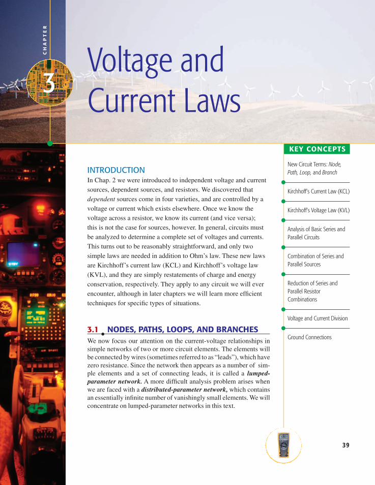
■ FIGURE 3.1 (a) A circuit containing three nodesand five branches. (b) Node 1 is redrawn to look liketwo nodes; it is still one node.
(a)
1
2
3
(b)
1
2
3
A point at which two or more elements have a common connection iscalled a node. For example, Fig. 3.1a shows a circuit containing threenodes. Sometimes networks are drawn so as to trap an unwary student intobelieving that there are more nodes present than is actually the case. Thisoccurs when a node, such as node 1 in Fig. 3.1a, is shown as two separatejunctions connected by a (zero-resistance) conductor, as in Fig. 3.1b. How-ever, all that has been done is to spread the common point out into acommon zero-resistance line. Thus, we must necessarily consider all of theperfectly conducting leads or portions of leads attached to the node as partof the node. Note also that every element has a node at each of its ends.
Suppose that we start at one node in a network and move through a sim-ple element to the node at the other end. We then continue from that nodethrough a different element to the next node, and continue this movementuntil we have gone through as many elements as we wish. If no node wasencountered more than once, then the set of nodes and elements that wehave passed through is defined as a path. If the node at which we started isthe same as the node on which we ended, then the path is, by definition, aclosed path or a loop.
For example, in Fig. 3.1a, if we move from node 2 through the currentsource to node 1, and then through the upper right resistor to node 3, wehave established a path; since we have not continued on to node 2 again, wehave not made a loop. If we proceeded from node 2 through the currentsource to node 1, down through the left resistor to node 2, and then upthrough the central resistor to node 1 again, we do not have a path, since anode (actually two nodes) was encountered more than once; we also do nothave a loop, because a loop must be a path.
Another term whose use will prove convenient is branch. We define abranch as a single path in a network, composed of one simple element andthe node at each end of that element. Thus, a path is a particular collectionof branches. The circuit shown in Fig. 3.1a and b contains five branches.
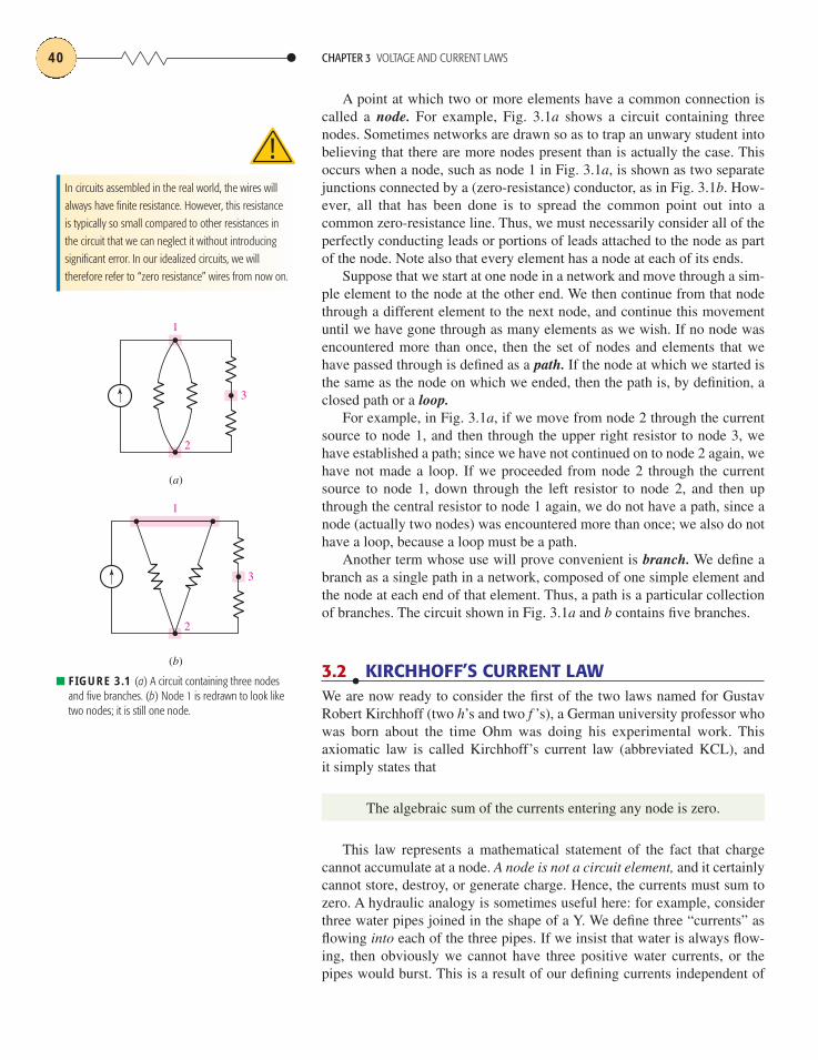
3.2 • KIRCHHOFF’S CURRENT LAWWe are now ready to consider the first of the two laws named for GustavRobert Kirchhoff (two h’s and two f ’s), a German university professor whowas born about the time Ohm was doing his experimental work. Thisaxiomatic law is called Kirchhoff’s current law (abbreviated KCL), andit simply states that
The algebraic sum of the currents entering any node is zero.
This law represents a mathematical statement of the fact that chargecannot accumulate at a node. A node is not a circuit element, and it certainlycannot store, destroy, or generate charge. Hence, the currents must sum tozero. A hydraulic analogy is sometimes useful here: for example, considerthree water pipes joined in the shape of a Y. We define three “currents” asflowing into each of the three pipes. If we insist that water is always flow-ing, then obviously we cannot have three positive water currents, or thepipes would burst. This is a result of our defining currents independent of
SECTION 3.2 KIRCHHOFF’S CURRENT LAW 41
the direction that water is actually flowing. Therefore, the value of eitherone or two of the currents as defined must be negative.
Consider the node shown in Fig. 3.2. The algebraic sum of the four cur-rents entering the node must be zero:
iA + iB + (−iC) + (−iD) = 0
However, the law could be equally well applied to the algebraic sum ofthe currents leaving the node:
(−iA) + (−iB) + iC + iD = 0
We might also wish to equate the sum of the currents having referencearrows directed into the node to the sum of those directed out of the node:
iA + iB = iC + iD
which simply states that the sum of the currents going in must equal the sumof the currents going out.
■ FIGURE 3.2 Example node to illustrate the applica-tion of Kirchhoff’s current law.
iC
iBiA
iD
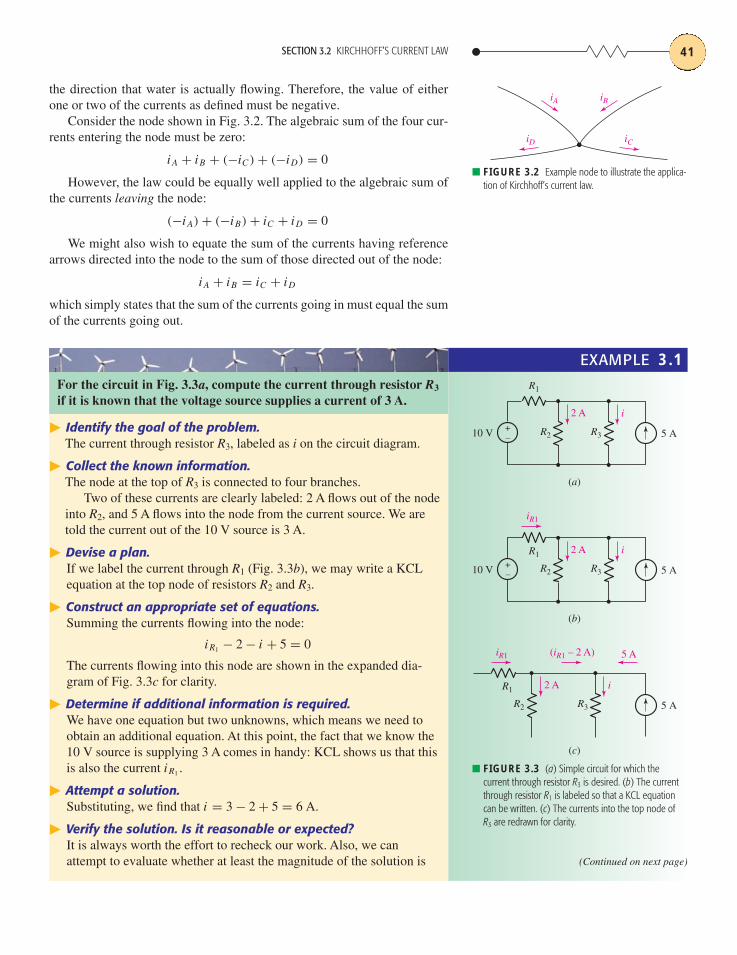
For the circuit in Fig. 3.3a, compute the current through resistor R3if it is known that the voltage source supplies a current of 3 A.
� Identify the goal of the problem.The current through resistor R3, labeled as i on the circuit diagram.
� Collect the known information.The node at the top of R3 is connected to four branches.
Two of these currents are clearly labeled: 2 A flows out of the nodeinto R2, and 5 A flows into the node from the current source. We aretold the current out of the 10 V source is 3 A.
� Devise a plan.If we label the current through R1 (Fig. 3.3b), we may write a KCLequation at the top node of resistors R2 and R3.
� Construct an appropriate set of equations.Summing the currents flowing into the node:
iR1 − 2 − i + 5 = 0
The currents flowing into this node are shown in the expanded dia-gram of Fig. 3.3c for clarity.
� Determine if additional information is required.We have one equation but two unknowns, which means we need toobtain an additional equation. At this point, the fact that we know the10 V source is supplying 3 A comes in handy: KCL shows us that thisis also the current iR1 .
� Attempt a solution.Substituting, we find that i = 3 − 2 + 5 = 6 A.
� Verify the solution. Is it reasonable or expected?It is always worth the effort to recheck our work. Also, we canattempt to evaluate whether at least the magnitude of the solution is
EXAMPLE 3.1
(Continued on next page)
■ FIGURE 3.3 (a) Simple circuit for which thecurrent through resistor R3 is desired. (b) The currentthrough resistor R1 is labeled so that a KCL equationcan be written. (c) The currents into the top node of R3 are redrawn for clarity.
(a)
+–
R2 R3
R1
5 A10 V
i2 A
(c)
R2 R3
R1
5 A
5 A
i2 A
iR1 (iR1 – 2 A)
(b)
+–
R2 R3
R1
5 A10 V
i2 A
iR1
CHAPTER 3 VOLTAGE AND CURRENT LAWS42
■ FIGURE 3.5 The potential difference betweenpoints A and B is independent of the path selected.
v1
+
–v3
–
+
v2+ –
A C
B
1
2
3
A compact expression for Kirchhoff’s current law is N∑
n=1
in = 0 [1]
which is just a shorthand statement for
i1 + i2 + i3 + · · · + iN = 0 [2]
When Eq. [1] or Eq. [2] is used, it is understood that the N currentarrows are either all directed toward the node in question, or are all directedaway from it.
3.3 • KIRCHHOFF’S VOLTAGE LAWCurrent is related to the charge flowing through a circuit element, whereasvoltage is a measure of potential energy difference across the element.There is a single unique value for any voltage in circuit theory. Thus, the en-ergy required to move a unit charge from point A to point B in a circuit musthave a value independent of the path chosen to get from A to B (there isoften more than one such path). We may assert this fact through Kirchhoff’svoltage law (abbreviated KVL):
The algebraic sum of the voltages around any closed path is zero.
In Fig. 3.5, if we carry a charge of 1 C from A to B through element 1,the reference polarity signs for v1 show that we do v1 joules of work.1 Now
(1) Note that we chose a 1 C charge for the sake of numerical convenience: therefore, we did (1 C)(v1 J/C) = v1 joules of work.
reasonable. In this case, we have two sources—one supplies 5 A, andthe other supplies 3 A. There are no other sources, independent ordependent. Thus, we would not expect to find any current in thecircuit in excess of 8 A.
PRACTICE ●
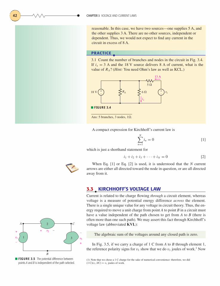
3.1 Count the number of branches and nodes in the circuit in Fig. 3.4.If ix = 3 A and the 18 V source delivers 8 A of current, what is thevalue of RA? (Hint: You need Ohm’s law as well as KCL.)
Ans: 5 branches, 3 nodes, 1�.
■ FIGURE 3.4
+–
+–
vxRA
13 A
ix
5 �
6 �18 V

SECTION 3.3 KIRCHHOFF’S VOLTAGE LAW 43
if, instead, we choose to proceed from A to B via node C, then we expend(v2 − v3) joules of energy. The work done, however, is independent of thepath in a circuit, and so any route must lead to the same value for the volt-age. In other words,
v1 = v2 − v3 [3]
It follows that if we trace out a closed path, the algebraic sum of the volt-ages across the individual elements around it must be zero. Thus, we maywrite
v1 + v2 + v3 + · · · + vN = 0
or, more compactly, N∑
n=1
vn = 0 [4]
We can apply KVL to a circuit in several different ways. One methodthat leads to fewer equation-writing errors than others consists of movingmentally around the closed path in a clockwise direction and writing downdirectly the voltage of each element whose (+) terminal is entered, andwriting down the negative of every voltage first met at the (−) sign. Apply-ing this to the single loop of Fig. 3.5, we have
−v1 + v2 − v3 = 0
which agrees with our previous result, Eq. [3].
In the circuit of Fig. 3.6, find vx and ix.
We know the voltage across two of the three elements in the circuit.Thus, KVL can be applied immediately to obtain vx .
Beginning with the bottom node of the 5 V source, we apply KVLclockwise around the loop:
−5 − 7 + vx = 0
so vx = 12 V.KCL applies to this circuit, but only tells us that the same current
(ix ) flows through all three elements. We now know the voltage acrossthe 100 � resistor, however.
Invoking Ohm’s law,
ix = vx
100= 12
100A = 120 mA
PRACTICE ●
3.2 Determine ix and vx in the circuit of Fig. 3.7.
Ans: vx = −4 V; ix = −400 mA.
EXAMPLE 3.2
■ FIGURE 3.6 A simple circuit with two voltagesources and a single resistor.
+–
+–
5 V
7 V
100 � vx
+
–
ix
■ FIGURE 3.7
+–
+ –
3 V
1 V
10 � vx
+
–
ix
CHAPTER 3 VOLTAGE AND CURRENT LAWS44
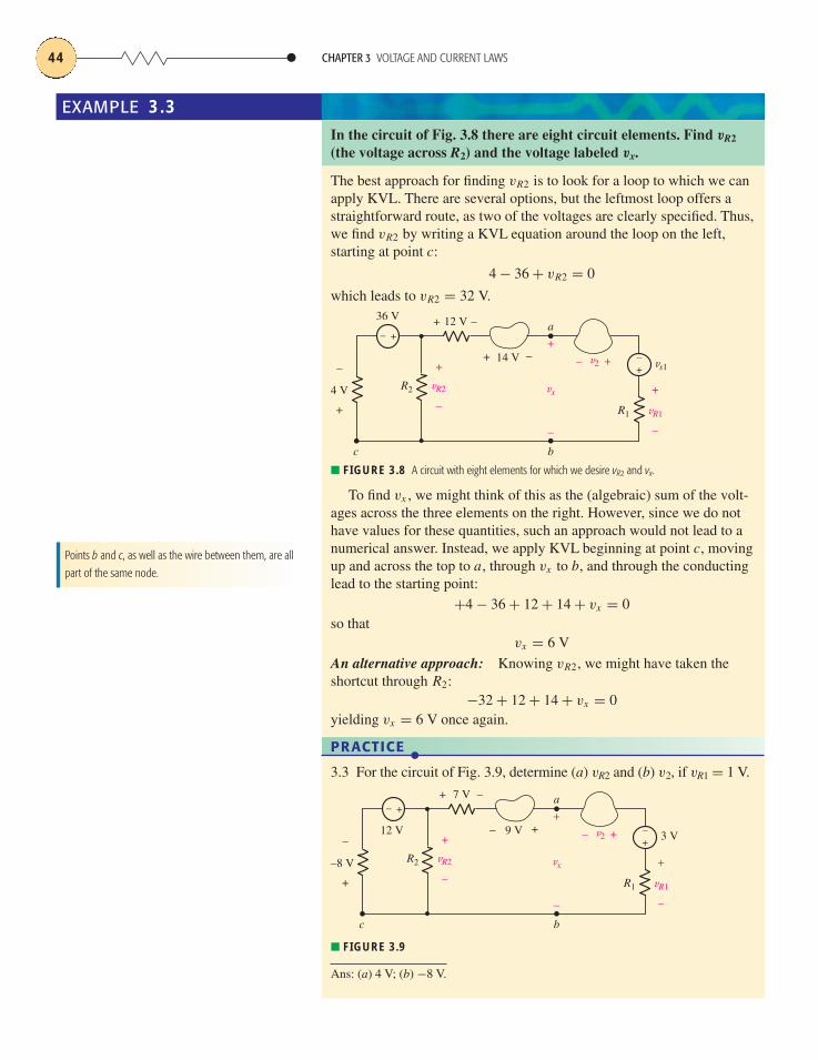
EXAMPLE 3.3In the circuit of Fig. 3.8 there are eight circuit elements. Find vR2(the voltage across R2) and the voltage labeled vx.
The best approach for finding vR2 is to look for a loop to which we canapply KVL. There are several options, but the leftmost loop offers astraightforward route, as two of the voltages are clearly specified. Thus,we find vR2 by writing a KVL equation around the loop on the left,starting at point c:
4 − 36 + vR2 = 0
which leads to vR2 = 32 V.
To find vx , we might think of this as the (algebraic) sum of the volt-ages across the three elements on the right. However, since we do nothave values for these quantities, such an approach would not lead to anumerical answer. Instead, we apply KVL beginning at point c, movingup and across the top to a, through vx to b, and through the conductinglead to the starting point:
+4 − 36 + 12 + 14 + vx = 0so that
vx = 6 V
An alternative approach: Knowing vR2, we might have taken theshortcut through R2:
−32 + 12 + 14 + vx = 0yielding vx = 6 V once again.
■ FIGURE 3.8 A circuit with eight elements for which we desire vR2 and vx.
+–
+–
4 V
–
+
vx
+
–
vR2
–
+
vR1
+
–
v2 +–
+ –12 V
+ –14 V
R1
R2
vs1
bc
a36 V
Points b and c, as well as the wire between them, are all
part of the same node.
PRACTICE ●
3.3 For the circuit of Fig. 3.9, determine (a) vR2 and (b) v2, if vR1 = 1 V.
■ FIGURE 3.9
+–
+–
–8 V
–
+
vx
+
–
vR2
–
+
vR1
+
–
v2 +–
+ –7 V
– +9 V12 V
R1
R2
3 V
bc
a
Ans: (a) 4 V; (b) −8 V.
SECTION 3.3 KIRCHHOFF’S VOLTAGE LAW 45
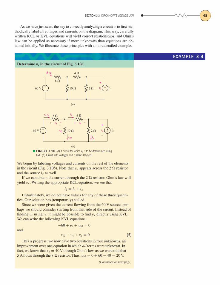
Determine vx in the circuit of Fig. 3.10a.
EXAMPLE 3.4
+–
vx
(a)
4 �
8 �
2 �10 �60 V ix
+
–
5 A
+–
vx
(b)
4 �8 �
2 �10 �60 V ix
+
–
5 A
v10
+
–
v4+ –v8+ –
i4
i10 i2
■ FIGURE 3.10 (a) A circuit for which vx is to be determined usingKVL. (b) Circuit with voltages and currents labeled.
We begin by labeling voltages and currents on the rest of the elementsin the circuit (Fig. 3.10b). Note that vx appears across the 2 � resistorand the source ix as well.
If we can obtain the current through the 2 � resistor, Ohm’s law willyield vx . Writing the appropriate KCL equation, we see that
i2 = i4 + ix
Unfortunately, we do not have values for any of these three quanti-ties. Our solution has (temporarily) stalled.
Since we were given the current flowing from the 60 V source, per-haps we should consider starting from that side of the circuit. Instead offinding vx using i2, it might be possible to find vx directly using KVL.We can write the following KVL equations:
−60 + v8 + v10 = 0and
−v10 + v4 + vx = 0 [5]
This is progress: we now have two equations in four unknowns, animprovement over one equation in which all terms were unknown. Infact, we know that v8 = 40 V through Ohm’s law, as we were told that5 A flows through the 8 � resistor. Thus, v10 = 0 + 60 − 40 = 20 V,
(Continued on next page)
As we have just seen, the key to correctly analyzing a circuit is to first me-thodically label all voltages and currents on the diagram. This way, carefullywritten KCL or KVL equations will yield correct relationships, and Ohm’slaw can be applied as necessary if more unknowns than equations are ob-tained initially. We illustrate these principles with a more detailed example.

so Eq. [5] reduces tovx = 20 − v4
If we can determine v4, the problem is solved.The best route to finding a numerical value for the voltage v4 in this
case is to employ Ohm’s law, which requires a value for i4. From KCL,we see that
i4 = 5 − i10 = 5 − v10
10= 5 − 20
10= 3
so that v4 = (4)(3) = 12 V and hence vx = 20 − 12 = 8 V.
CHAPTER 3 VOLTAGE AND CURRENT LAWS46
■ FIGURE 3.12 (a) A single-loop circuit with fourelements. (b) The circuit model with source voltagesand resistance values given. (c) Current and voltagereference signs have been added to the circuit.
(a)
+–
+–
+ –
vs1
vs2
(b)
R1
R2
i
vR2
+
–
vR1+ –
i
ii
+–
+ –
vs1
vs2
(c)
R1
R2
3.4 • THE SINGLE-LOOP CIRCUITWe have seen that repeated use of KCL and KVL in conjunction with Ohm’slaw can be applied to nontrivial circuits containing several loops and a num-ber of different elements. Before proceeding further, this is a good time tofocus on the concept of series (and, in the next section, parallel) circuits, asthey form the basis of any network we will encounter in the future.
All of the elements in a circuit that carry the same current are said to beconnected in series. As an example, consider the circuit of Fig. 3.10. The60 V source is in series with the 8 � resistor; they carry the same 5 A cur-rent. However, the 8 � resistor is not in series with the 4 � resistor; theycarry different currents. Note that elements may carry equal currents andnot be in series; two 100 W light bulbs in neighboring houses may very wellcarry equal currents, but they certainly do not carry the same current and arenot connected in series.
Figure 3.12a shows a simple circuit consisting of two batteries andtwo resistors. Each terminal, connecting lead, and solder glob is assumed tohave zero resistance; together they constitute an individual node of the circuitdiagram in Fig. 3.12b. Both batteries are modeled by ideal voltage sources;any internal resistances they may have are assumed to be small enough toneglect. The two resistors are assumed to be ideal (linear) resistors.
We seek the current through each element, the voltage across each ele-ment, and the power absorbed by each element. Our first step in the analy-sis is the assumption of reference directions for the unknown currents.Arbitrarily, let us select a clockwise current i which flows out of the upperterminal of the voltage source on the left. This choice is indicated by an ar-row labeled i at that point in the circuit, as shown in Fig. 3.12c. A trivial
PRACTICE ●
3.4 Determine vx in the circuit of Fig. 3.11.
Ans: vx = 12.8 V.
■ FIGURE 3.11
+–
vx
2 �
8 �
2 �10 �30 V ix
+
–
2 A
SECTION 3.4 THE SINGLE-LOOP CIRCUIT 47
application of Kirchhoff’s current law assures us that this same current mustalso flow through every other element in the circuit; we emphasize this factthis one time by placing several other current symbols about the circuit.
Our second step in the analysis is a choice of the voltage reference for eachof the two resistors. The passive sign convention requires that the resistor cur-rent and voltage variables be defined so that the current enters the terminal atwhich the positive voltage reference is located. Since we already (arbitrarily)selected the current direction,vR1 andvR2 are defined as in Fig. 3.12c.
The third step is the application of Kirchhoff’s voltage law to the onlyclosed path. Let us decide to move around the circuit in the clockwisedirection, beginning at the lower left corner, and to write down directlyevery voltage first met at its positive reference, and to write down the nega-tive of every voltage encountered at the negative terminal. Thus,
−vs1 + vR1 + vs2 + vR2 = 0 [6]
We then apply Ohm’s law to the resistive elements:
vR1 = R1i and vR2 = R2i
Substituting into Eq. [6] yields
−vs1 + R1i + vs2 + R2i = 0
Since i is the only unknown, we find that
i = vs1 − vs2
R1 + R2
The voltage or power associated with any element may now be obtained byapplying v = Ri, p = vi , or p = i2R.
PRACTICE ●
3.5 In the circuit of Fig. 3.12b, vs1 = 120 V, vs2 = 30 V, R1 = 30 �,and R2 = 15 �. Compute the power absorbed by each element.
Ans: p120V = −240 W; p30V = +60 W; p30� = 120 W; p15� = 60 W.
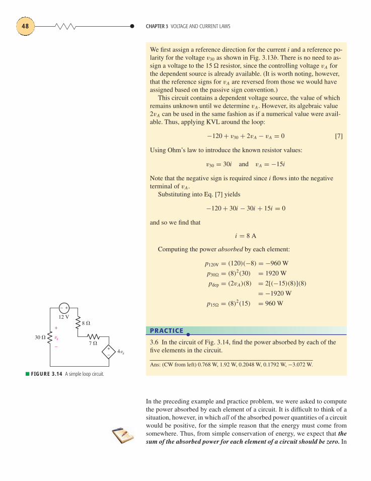
EXAMPLE 3.5
Compute the power absorbed in each element for the circuit shownin Fig. 3.13a.
(Continued on next page)
2vA
30 �
15 �
+ –
120 V+
–vA
–
+
(a) (b)
i2vA
30 �
15 �
v30++
––
120 V+
–
vA
–
+
■ FIGURE 3.13 (a) A single-loop circuit containing a dependent source. (b) The current i andvoltage v30 are assigned.
CHAPTER 3 VOLTAGE AND CURRENT LAWS48
We first assign a reference direction for the current i and a reference po-larity for the voltage v30 as shown in Fig. 3.13b. There is no need to as-sign a voltage to the 15 � resistor, since the controlling voltage vA forthe dependent source is already available. (It is worth noting, however,that the reference signs for vA are reversed from those we would haveassigned based on the passive sign convention.)
This circuit contains a dependent voltage source, the value of whichremains unknown until we determine vA. However, its algebraic value2vA can be used in the same fashion as if a numerical value were avail-able. Thus, applying KVL around the loop:
−120 + v30 + 2vA − vA = 0 [7]
Using Ohm’s law to introduce the known resistor values:
v30 = 30i and vA = −15i
Note that the negative sign is required since i flows into the negativeterminal of vA.
Substituting into Eq. [7] yields
−120 + 30i − 30i + 15i = 0
and so we find that
i = 8 A
Computing the power absorbed by each element:
p120v = (120)(−8) = −960 W
p30� = (8)2(30) = 1920 W
pdep = (2vA)(8) = 2[(−15)(8)](8)
= −1920 W
p15� = (8)2(15) = 960 W+–
12 V
30 �
8 �
7 �+–
vx
+
–4vx
■ FIGURE 3.14 A simple loop circuit.
In the preceding example and practice problem, we were asked to computethe power absorbed by each element of a circuit. It is difficult to think of asituation, however, in which all of the absorbed power quantities of a circuitwould be positive, for the simple reason that the energy must come fromsomewhere. Thus, from simple conservation of energy, we expect that thesum of the absorbed power for each element of a circuit should be zero. In
PRACTICE ●
3.6 In the circuit of Fig. 3.14, find the power absorbed by each of thefive elements in the circuit.
Ans: (CW from left) 0.768 W, 1.92 W, 0.2048 W, 0.1792 W, −3.072 W.

SECTION 3.5 THE SINGLE-NODE-PAIR CIRCUIT 49
other words, at least one of the quantities should be negative (neglecting thetrivial case where the circuit is not operating). Stated another way, the sumof the supplied power for each element should be zero. More pragmatically,the sum of the absorbed power equals the sum of the supplied power,which seems reasonable enough at face value.
Let’s test this with the circuit of Fig. 3.13 from Example 3.5, whichconsists of two sources (one dependent and one independent) and tworesistors. Adding the power absorbed by each element, we find∑
all elements
pabsorbed = −960 + 1920 − 1920 + 960 = 0
In reality (our indication is the sign associated with the absorbed power)the 120 V source supplies +960 W, and the dependent source supplies+1920 W. Thus, the sources supply a total of 960 + 1920 = 2880 W. Theresistors are expected to absorb positive power, which in this case sums to atotal of 1920 + 960 = 2880 W. Thus, if we take into account each elementof the circuit, ∑
pabsorbed =∑
psupplied
as we expect.Turning our attention to Practice Problem 3.6, the solution to which
the reader might want to verify, we see that the absorbed powers sumto 0.768 + 1.92 + 0.2048 + 0.1792 − 3.072 = 0. Interestingly enough, the12 V independent voltage source is absorbing +1.92 W, which means it isdissipating power, not supplying it. Instead, the dependent voltage sourceappears to be supplying all the power in this particular circuit. Is such athing possible? We usually expect a source to supply positive power, butsince we are employing idealized sources in our circuits, it is in fact possi-ble to have a net power flow into any source. If the circuit is changed insome way, the same source might then be found to supply positive power.The result is not known until a circuit analysis has been completed.
3.5 • THE SINGLE-NODE-PAIR CIRCUITThe companion of the single-loop circuit discussed in Sec. 3.4 is the single-node-pair circuit, in which any number of simple elements are connectedbetween the same pair of nodes. An example of such a circuit is shown inFig. 3.15a. KVL forces us to recognize that the voltage across each branchis the same as that across any other branch. Elements in a circuit having acommon voltage across them are said to be connected in parallel.
(Continued on next page)
Find the voltage, current, and power associated with each elementin the circuit of Fig. 3.15a.
We first define a voltage v and arbitrarily select its polarity as shown inFig. 3.15b. Two currents, flowing in the resistors, are selected in con-formance with the passive sign convention, as shown in Fig. 3.15b.
EXAMPLE 3.6
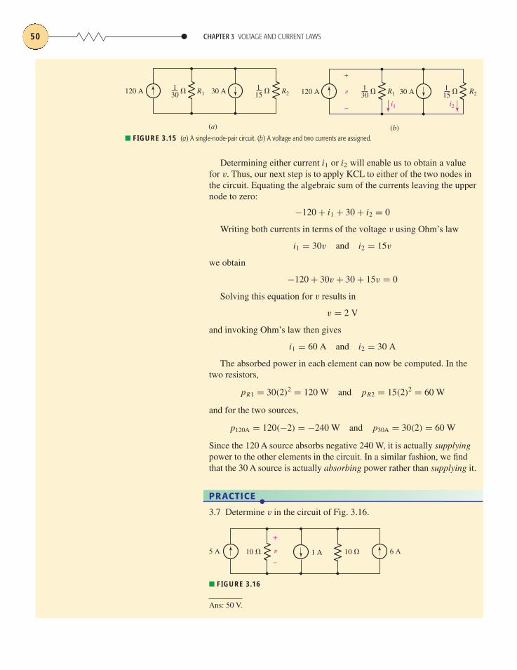
CHAPTER 3 VOLTAGE AND CURRENT LAWS50
5 A 6 A1 A10 � 10 �v
+
–
■ FIGURE 3.16
PRACTICE ●
3.7 Determine v in the circuit of Fig. 3.16.
Ans: 50 V.
(a)
�120 A 30 AR1 R2
(b)
120 A 30 AR1 R2v
+
– i1 i2
115�1
30 �115�1
30
■ FIGURE 3.15 (a) A single-node-pair circuit. (b) A voltage and two currents are assigned.
Determining either current i1 or i2 will enable us to obtain a valuefor v. Thus, our next step is to apply KCL to either of the two nodes inthe circuit. Equating the algebraic sum of the currents leaving the uppernode to zero:
−120 + i1 + 30 + i2 = 0
Writing both currents in terms of the voltage v using Ohm’s law
i1 = 30v and i2 = 15v
we obtain
−120 + 30v + 30 + 15v = 0
Solving this equation for v results in
v = 2 V
and invoking Ohm’s law then gives
i1 = 60 A and i2 = 30 A
The absorbed power in each element can now be computed. In thetwo resistors,
pR1 = 30(2)2 = 120 W and pR2 = 15(2)2 = 60 W
and for the two sources,
p120A = 120(−2) = −240 W and p30A = 30(2) = 60 W
Since the 120 A source absorbs negative 240 W, it is actually supplyingpower to the other elements in the circuit. In a similar fashion, we findthat the 30 A source is actually absorbing power rather than supplying it.
SECTION 3.6 SERIES AND PARALLEL CONNECTED SOURCES 51
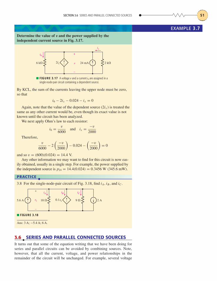
Determine the value of v and the power supplied by the independent current source in Fig. 3.17.
EXAMPLE 3.7
2 k�2ix6 k� 24 mAv
+
–
ix
i6
■ FIGURE 3.17 A voltage v and a current i6 are assigned in asingle-node-pair circuit containing a dependent source.
By KCL, the sum of the currents leaving the upper node must be zero,so that
i6 − 2ix − 0.024 − ix = 0
Again, note that the value of the dependent source (2ix ) is treated thesame as any other current would be, even though its exact value is notknown until the circuit has been analyzed.
We next apply Ohm’s law to each resistor:
i6 = v
6000and ix = −v
2000
Therefore,v
6000− 2
( −v
2000
)− 0.024 −
( −v
2000
)= 0
and so v = (600)(0.024) = 14.4 V.Any other information we may want to find for this circuit is now eas-
ily obtained, usually in a single step. For example, the power supplied bythe independent source is p24 = 14.4(0.024) = 0.3456 W (345.6 mW).
Ans: 3 A; −5.4 A; 6 A.
2 A0.1vx 9 �18 �5.6 A vx
+
–
iBiA iC
■ FIGURE 3.18
PRACTICE ●
3.8 For the single-node-pair circuit of Fig. 3.18, find iA, iB , and iC .
3.6 • SERIES AND PARALLEL CONNECTED SOURCESIt turns out that some of the equation writing that we have been doing forseries and parallel circuits can be avoided by combining sources. Note,however, that all the current, voltage, and power relationships in theremainder of the circuit will be unchanged. For example, several voltage
CHAPTER 3 VOLTAGE AND CURRENT LAWS52
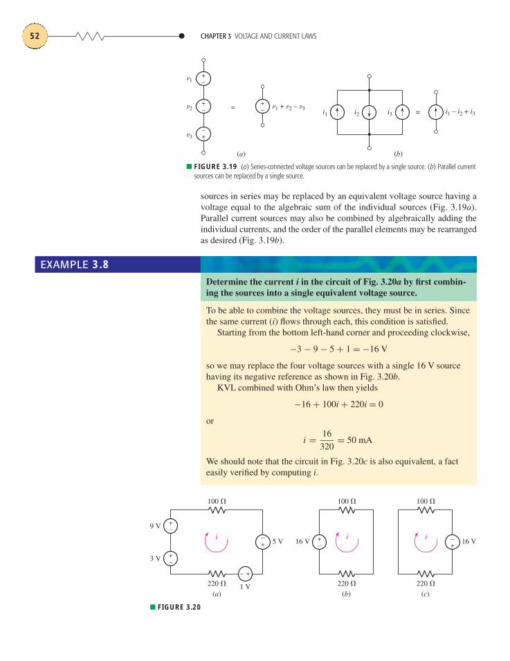
EXAMPLE 3.8Determine the current i in the circuit of Fig. 3.20a by first combin-ing the sources into a single equivalent voltage source.
To be able to combine the voltage sources, they must be in series. Sincethe same current (i) flows through each, this condition is satisfied.
Starting from the bottom left-hand corner and proceeding clockwise,
−3 − 9 − 5 + 1 = −16 V
so we may replace the four voltage sources with a single 16 V sourcehaving its negative reference as shown in Fig. 3.20b.
KVL combined with Ohm’s law then yields
−16 + 100i + 220i = 0
or
i = 16
320= 50 mA
We should note that the circuit in Fig. 3.20c is also equivalent, a facteasily verified by computing i.
(a)
+–
+–
9 V
5 V
1 V
3 V
–+
100 �
220 �(b)
+–
16 V
100 �
ii
(c)
–+
16 V
100 �
220 � 220 �
i
+–
■ FIGURE 3.20
=
(a)
v1
v2+– v1 + v2 – v3
v3
+–
+–
+–
■ FIGURE 3.19 (a) Series-connected voltage sources can be replaced by a single source. (b) Parallel currentsources can be replaced by a single source.
=
(b)
i1 i2 i3 i1 – i2 + i3
sources in series may be replaced by an equivalent voltage source having avoltage equal to the algebraic sum of the individual sources (Fig. 3.19a).Parallel current sources may also be combined by algebraically adding theindividual currents, and the order of the parallel elements may be rearrangedas desired (Fig. 3.19b).

SECTION 3.6 SERIES AND PARALLEL CONNECTED SOURCES 53
PRACTICE ●
3.9 Determine the current i in the circuit of Fig. 3.21 after first replac-ing the four sources with a single equivalent source.
Ans: −54 A.
+–4 V
3 V
5 V
–+
1 V
– +
–+
47 �
7 �
i
■ FIGURE 3.21
Determine the voltage v in the circuit of Fig. 3.22a by first combin-ing the sources into a single equivalent current source.
The sources may be combined if the same voltage appears across eachone, which we can easily verify is the case. Thus, we create a newsource, arrow pointing upward into the top node, by adding the currentsthat flow into that node:
2.5 − 2.5 − 3 = −3 A
One equivalent circuit is shown in Fig. 3.22b.KCL then allows us to write
−3 + v
5+ v
5= 0
Solving, we find v = 7.5 V.Another equivalent circuit is shown in Fig. 3.22c.
EXAMPLE 3.9
5 � 5 �v
+
–
2.5 A 2.5 A 3 A
(a)
5 � 5 �v
+
–
3 A
(c)
5 � 5 �v
+
–
–3 A
(b)
■ FIGURE 3.22(Continued on next page)
CHAPTER 3 VOLTAGE AND CURRENT LAWS54
PRACTICE ●
3.10 Determine the voltage v in the circuit of Fig. 3.23 after firstreplacing the three sources with a single equivalent source.
Ans: 50 V.
10 �10 � v
+
–
5 A 6 A1 A
■ FIGURE 3.23
To conclude the discussion of parallel and series source combinations,we should consider the parallel combination of two voltage sources and theseries combination of two current sources. For instance, what is the equiva-lent of a 5 V source in parallel with a 10 V source? By the definition of avoltage source, the voltage across the source cannot change; by Kirchhoff’svoltage law, then, 5 equals 10 and we have hypothesized a physical impos-sibility. Thus, ideal voltage sources in parallel are permissible only wheneach has the same terminal voltage at every instant. In a similar way, twocurrent sources may not be placed in series unless each has the same cur-rent, including sign, for every instant of time.
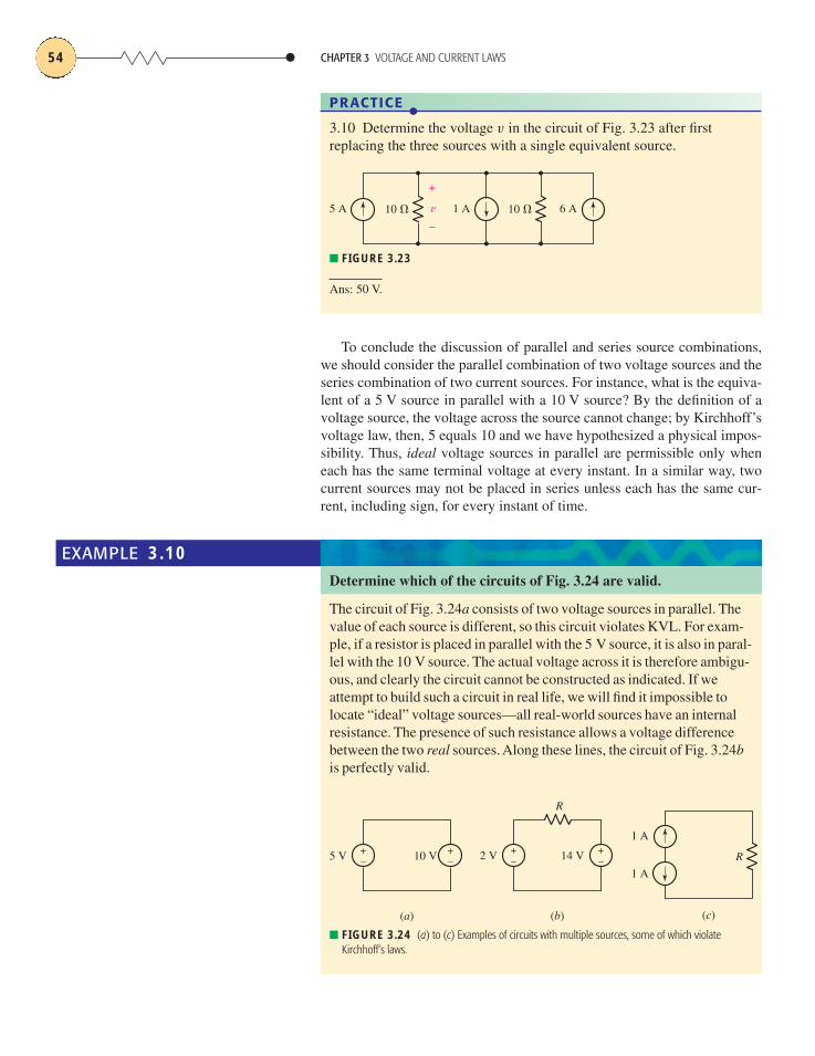
EXAMPLE 3.10Determine which of the circuits of Fig. 3.24 are valid.
The circuit of Fig. 3.24a consists of two voltage sources in parallel. Thevalue of each source is different, so this circuit violates KVL. For exam-ple, if a resistor is placed in parallel with the 5 V source, it is also in paral-lel with the 10 V source. The actual voltage across it is therefore ambigu-ous, and clearly the circuit cannot be constructed as indicated. If weattempt to build such a circuit in real life, we will find it impossible tolocate “ideal” voltage sources—all real-world sources have an internalresistance. The presence of such resistance allows a voltage differencebetween the two real sources. Along these lines, the circuit of Fig. 3.24bis perfectly valid.
+–5 V +
–10 V
(a)
+–
R
2 V +–14 V
(b)
R
1 A
1 A
(c)
■ FIGURE 3.24 (a) to (c) Examples of circuits with multiple sources, some of which violateKirchhoff’s laws.
SECTION 3.7 RESISTORS IN SERIES AND PARALLEL 55
The circuit of Fig. 3.24c violates KCL: it is unclear what currentactually flows through the resistor R.
PRACTICE ●
3.11 Determine whether the circuit of Fig. 3.25 violates either ofKirchhoff’s laws.
Ans: No. If the resistor were removed, however, the resulting circuit would.
R5 A 3 A
■ FIGURE 3.25
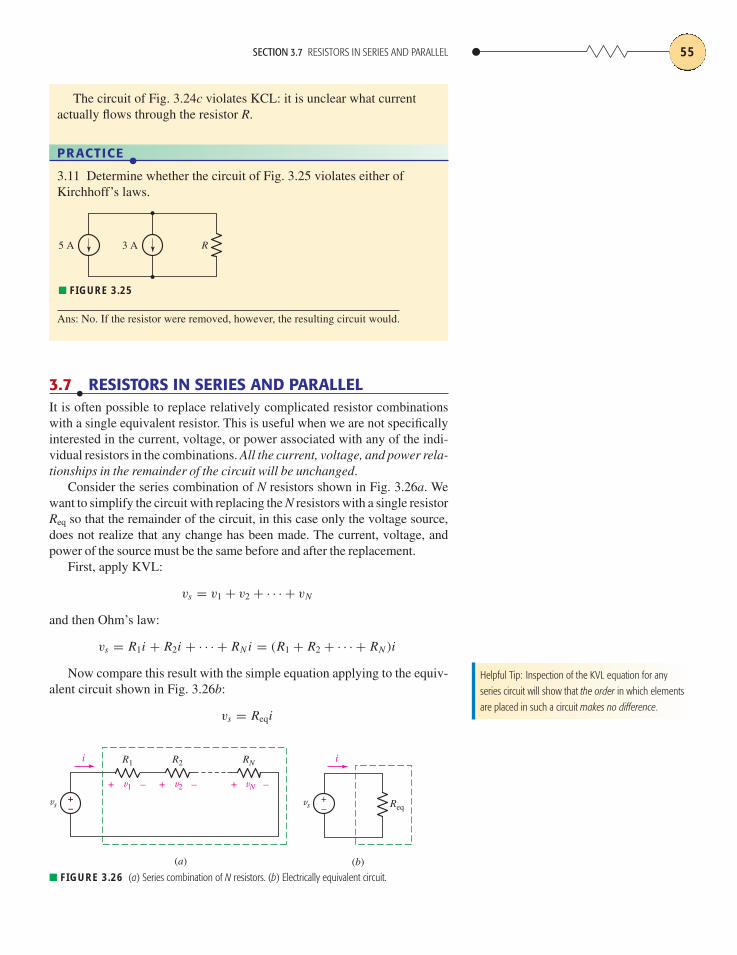
3.7 • RESISTORS IN SERIES AND PARALLELIt is often possible to replace relatively complicated resistor combinationswith a single equivalent resistor. This is useful when we are not specificallyinterested in the current, voltage, or power associated with any of the indi-vidual resistors in the combinations. All the current, voltage, and power rela-tionships in the remainder of the circuit will be unchanged.
Consider the series combination of N resistors shown in Fig. 3.26a. Wewant to simplify the circuit with replacing the N resistors with a single resistorReq so that the remainder of the circuit, in this case only the voltage source,does not realize that any change has been made. The current, voltage, andpower of the source must be the same before and after the replacement.
First, apply KVL:
vs = v1 + v2 + · · · + vN
and then Ohm’s law:
vs = R1i + R2i + · · · + RN i = (R1 + R2 + · · · + RN )i
Now compare this result with the simple equation applying to the equiv-alent circuit shown in Fig. 3.26b:
vs = Reqi
v1+ – v2+ – vN+ –
(a)
R1 R2 RN
vs++––
i
(b)
Reqvs
+–
i
■ FIGURE 3.26 (a) Series combination of N resistors. (b) Electrically equivalent circuit.
Helpful Tip: Inspection of the KVL equation for any
series circuit will show that the order in which elements
are placed in such a circuit makes no difference.
Thus, the value of the equivalent resistance for N series resistors is
[8]
We are therefore able to replace a two-terminal network consisting of Nseries resistors with a single two-terminal element Req that has the same v-i relationship.
It should be emphasized again that we might be interested in the current,voltage, or power of one of the original elements. For example, the voltageof a dependent voltage source may depend upon the voltage across R3.Once R3 is combined with several series resistors to form an equivalent re-sistance, then it is gone and the voltage across it cannot be determined untilR3 is identified by removing it from the combination. In that case, it wouldhave been better to look ahead and not make R3 a part of the combinationinitially.
Req = R1 + R2 + · · · + RN
CHAPTER 3 VOLTAGE AND CURRENT LAWS56
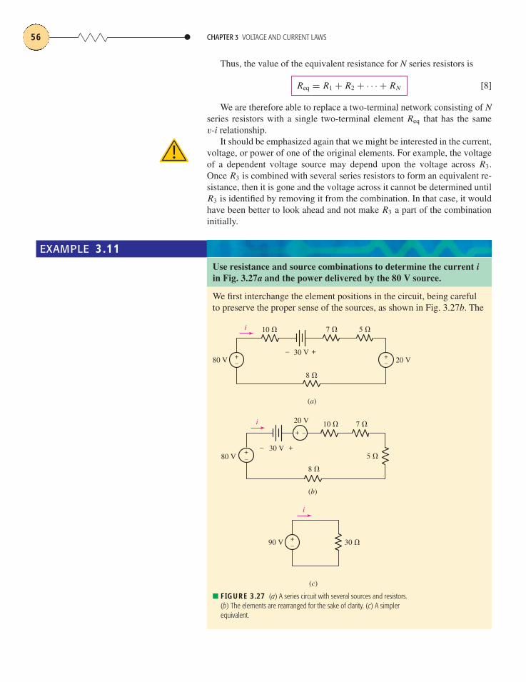
EXAMPLE 3.11Use resistance and source combinations to determine the current iin Fig. 3.27a and the power delivered by the 80 V source.
We first interchange the element positions in the circuit, being carefulto preserve the proper sense of the sources, as shown in Fig. 3.27b. The
30 V– +
(a)
80 V +–
+–
i
8 �
10 � 7 �
20 V
5 �
+–
+ –
i
80 V
10 �
30 V
20 V
– +
8 �
7 �
5 �
(b)
(c)
90 V +–
i
30 �
■ FIGURE 3.27 (a) A series circuit with several sources and resistors.(b) The elements are rearranged for the sake of clarity. (c) A simplerequivalent.
SECTION 3.7 RESISTORS IN SERIES AND PARALLEL 57
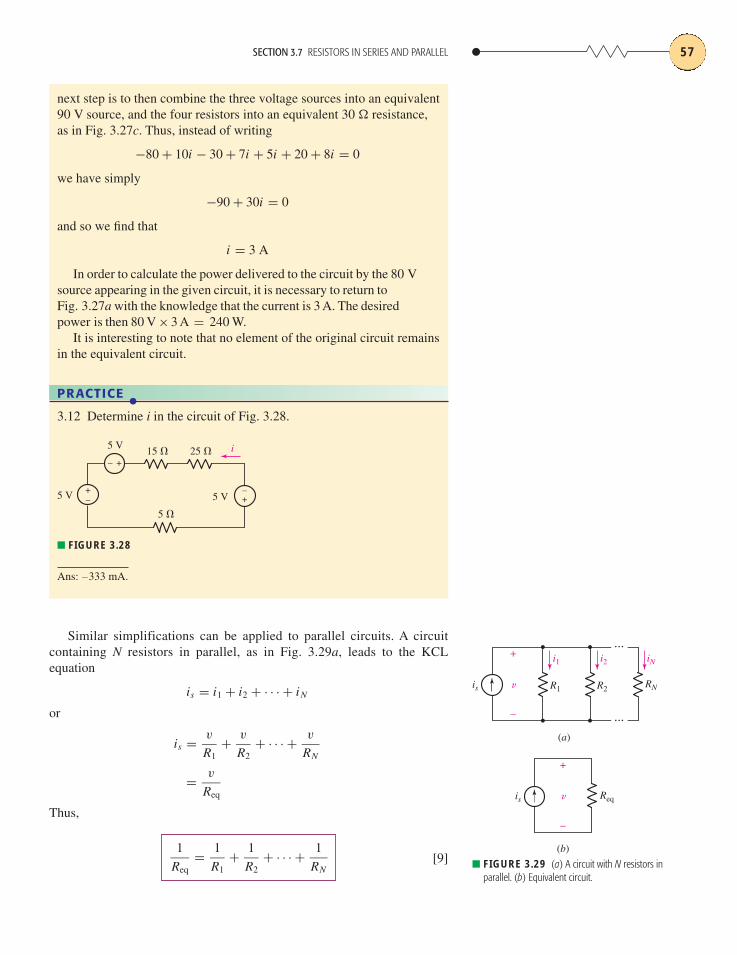
Similar simplifications can be applied to parallel circuits. A circuitcontaining N resistors in parallel, as in Fig. 3.29a, leads to the KCLequation
is = i1 + i2 + · · · + iN
or
is = v
R1+ v
R2+ · · · + v
RN
= v
Req
Thus,
[9]1
Req= 1
R1+ 1
R2+ · · · + 1
RN
next step is to then combine the three voltage sources into an equivalent90 V source, and the four resistors into an equivalent 30 � resistance,as in Fig. 3.27c. Thus, instead of writing
−80 + 10i − 30 + 7i + 5i + 20 + 8i = 0
we have simply
−90 + 30i = 0
and so we find that
i = 3 A
In order to calculate the power delivered to the circuit by the 80 Vsource appearing in the given circuit, it is necessary to return toFig. 3.27a with the knowledge that the current is 3 A. The desiredpower is then 80 V × 3 A � 240 W.
It is interesting to note that no element of the original circuit remainsin the equivalent circuit.
PRACTICE ●
3.12 Determine i in the circuit of Fig. 3.28.
Ans: −333 mA.
+– +
–
+–
i
5 V 5 V
15 �5 V
5 �
25 �
■ FIGURE 3.28
R2R1is RNv
+
–
i2i1 iN
(a)
...
...
is Reqv
+
–
(b)
■ FIGURE 3.29 (a) A circuit with N resistors inparallel. (b) Equivalent circuit.

CHAPTER 3 VOLTAGE AND CURRENT LAWS58
which can be written as
R−1eq = R−1
1 + R−12 + · · · + R−1
N
or, in terms of conductances, as
Geq = G1 + G2 + · · · + G N
The simplified (equivalent) circuit is shown in Fig. 3.29b.A parallel combination is routinely indicated by the following shorthand
notation:
Req = R1‖R2‖R3
The special case of only two parallel resistors is encountered fairly of-ten, and is given by
Req = R1‖R2
= 11
R1+ 1
R2
Or, more simply,
[10]
The last form is worth memorizing, although it is a common error toattempt to generalize Eq. [10] to more than two resistors, e.g.,
Req = R1 R2 R3
R1 + R2 + R3
A quick look at the units of this equation will immediately show that theexpression cannot possibly be correct.
Req = R1 R2
R1 + R2
PRACTICE ●
3.13 Determine v in the circuit of Fig. 3.30 by first combining the threecurrent sources, and then the two 10 � resistors.
Ans: 50 V.
10 �10 � v
+
–
5 A 6 A1 A
■ FIGURE 3.30
SECTION 3.7 RESISTORS IN SERIES AND PARALLEL 59
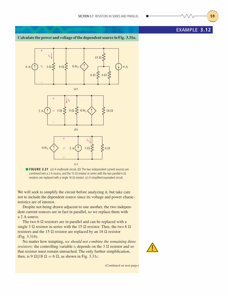
Calculate the power and voltage of the dependent source in Fig. 3.31a.
EXAMPLE 3.12
4 A0.9i3
15 �
6 � 6 �
3 �6 A vx
+
–
i3
9 �
(a)
0.9i33 � 9 � 18 �
(b)
2 A v
+
–
i3
0.9i3 3 �2 A 6 �v
+
–
i3
(c)
■ FIGURE 3.31 (a) A multinode circuit. (b) The two independent current sources arecombined into a 2 A source, and the 15 � resistor in series with the two parallel 6 �
resistors are replaced with a single 18 � resistor. (c) A simplified equivalent circuit.
We will seek to simplify the circuit before analyzing it, but take carenot to include the dependent source since its voltage and power charac-teristics are of interest.
Despite not being drawn adjacent to one another, the two indepen-dent current sources are in fact in parallel, so we replace them witha 2 A source.
The two 6 � resistors are in parallel and can be replaced with asingle 3 � resistor in series with the 15 � resistor. Thus, the two 6 �resistors and the 15 � resistor are replaced by an 18 � resistor(Fig. 3.31b).
No matter how tempting, we should not combine the remaining threeresistors; the controlling variable i3 depends on the 3 � resistor and sothat resistor must remain untouched. The only further simplification,then, is 9 �‖18 � = 6 �, as shown in Fig. 3.31c.
(Continued on next page)
CHAPTER 3 VOLTAGE AND CURRENT LAWS60
5 �
5 �
6 � 9 �
3 �3 �
3 � 3 �
1 A vx
+
–
i3
■ FIGURE 3.32
Applying KCL at the top node of Fig. 3.31c, we have
−0.9i3 − 2 + i3 + v
6= 0
Employing Ohm’s law,
v = 3i3
which allows us to compute
i3 = 10
3A
Thus, the voltage across the dependent source (which is the same asthe voltage across the 3 � resistor) is
v = 3i3 = 10 V
The dependent source therefore furnishes v × 0.9i3 =10(0.9)(10/3) = 30 W to the remainder of the circuit.
Now if we are later asked for the power dissipated in the 15 � resis-tor, we must return to the original circuit. This resistor is in series withan equivalent 3 � resistor; a voltage of 10 V is across the 18 � total;therefore, a current of 5/9 A flows through the 15 � resistor and thepower absorbed by this element is (5/9)2(15) or 4.63 W.
PRACTICE ●
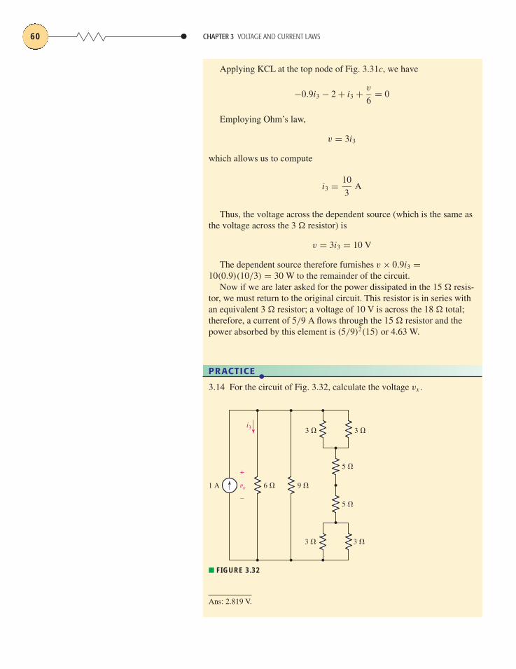
3.14 For the circuit of Fig. 3.32, calculate the voltage vx .
Ans: 2.819 V.
SECTION 3.8 VOLTAGE AND CURRENT DIVISION 61
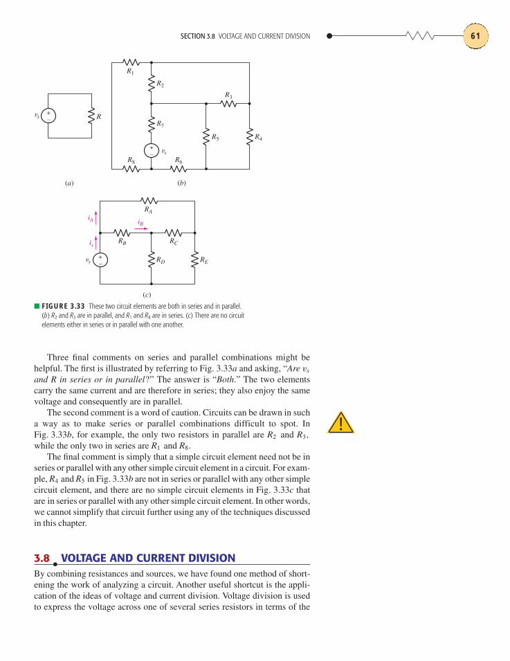
Three final comments on series and parallel combinations might behelpful. The first is illustrated by referring to Fig. 3.33a and asking, “Are vs
and R in series or in parallel?” The answer is “Both.” The two elementscarry the same current and are therefore in series; they also enjoy the samevoltage and consequently are in parallel.
The second comment is a word of caution. Circuits can be drawn in sucha way as to make series or parallel combinations difficult to spot. InFig. 3.33b, for example, the only two resistors in parallel are R2 and R3,
while the only two in series are R1 and R8.
The final comment is simply that a simple circuit element need not be inseries or parallel with any other simple circuit element in a circuit. For exam-ple, R4 and R5 in Fig. 3.33b are not in series or parallel with any other simplecircuit element, and there are no simple circuit elements in Fig. 3.33c thatare in series or parallel with any other simple circuit element. In other words,we cannot simplify that circuit further using any of the techniques discussedin this chapter.
3.8 • VOLTAGE AND CURRENT DIVISIONBy combining resistances and sources, we have found one method of short-ening the work of analyzing a circuit. Another useful shortcut is the appli-cation of the ideas of voltage and current division. Voltage division is usedto express the voltage across one of several series resistors in terms of the
+–
(a)
vs R
(b)
vs+–
R3
R2
R1
R7
R5 R4
R6R8
(c)
vs+–
RCRB
RA
RD RE
iBiA
is
■ FIGURE 3.33 These two circuit elements are both in series and in parallel. (b) R2 and R3 are in parallel, and R1 and R8 are in series. (c) There are no circuitelements either in series or in parallel with one another.
voltage across the combination. In Fig. 3.34, the voltage across R2 is foundvia KVL and Ohm’s law:
v = v1 + v2 = iR1 + iR2 = i(R1 + R2)
so
i = v
R1 + R2
Thus,
v2 = iR2 =(
v
R1 + R2
)R2
or
v2 = R2
R1 + R2v
and the voltage across R1 is, similarly,
v1 = R1
R1 + R2v
If the network of Fig. 3.34 is generalized by removing R2 and replacingit with the series combination of R2, R3, . . . , RN , then we have the generalresult for voltage division across a string of N series resistors
[11]
which allows us to compute the voltage vk that appears across an arbitraryresistor Rk of the series.
vk = Rk
R1 + R2 + · · · + RNv
CHAPTER 3 VOLTAGE AND CURRENT LAWS62
i
v2
+
–
v1+ –
v
+
–
R1
R2
■ FIGURE 3.34 An illustration of voltage division.
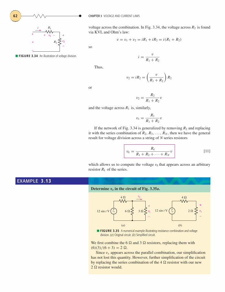
Determine vx in the circuit of Fig. 3.35a.
EXAMPLE 3.13
i3
vx
+
–
4 �
6 �12 sin t V 3 �+–
4 Ω
2 �
(b)(a)
12 sin t V vx
+
–
+–
■ FIGURE 3.35 A numerical example illustrating resistance combination and voltagedivision. (a) Original circuit. (b) Simplified circuit.
We first combine the 6 � and 3 � resistors, replacing them with(6)(3)/(6 + 3) = 2 �.
Since vx appears across the parallel combination, our simplificationhas not lost this quantity. However, further simplification of the circuitby replacing the series combination of the 4 � resistor with our new2 � resistor would.
SECTION 3.8 VOLTAGE AND CURRENT DIVISION 63
Thus, we proceed by simply applying voltage division to the circuitin Fig. 3.35b:
vx = (12 sin t)2
4 + 2= 4 sin t volts
PRACTICE ●
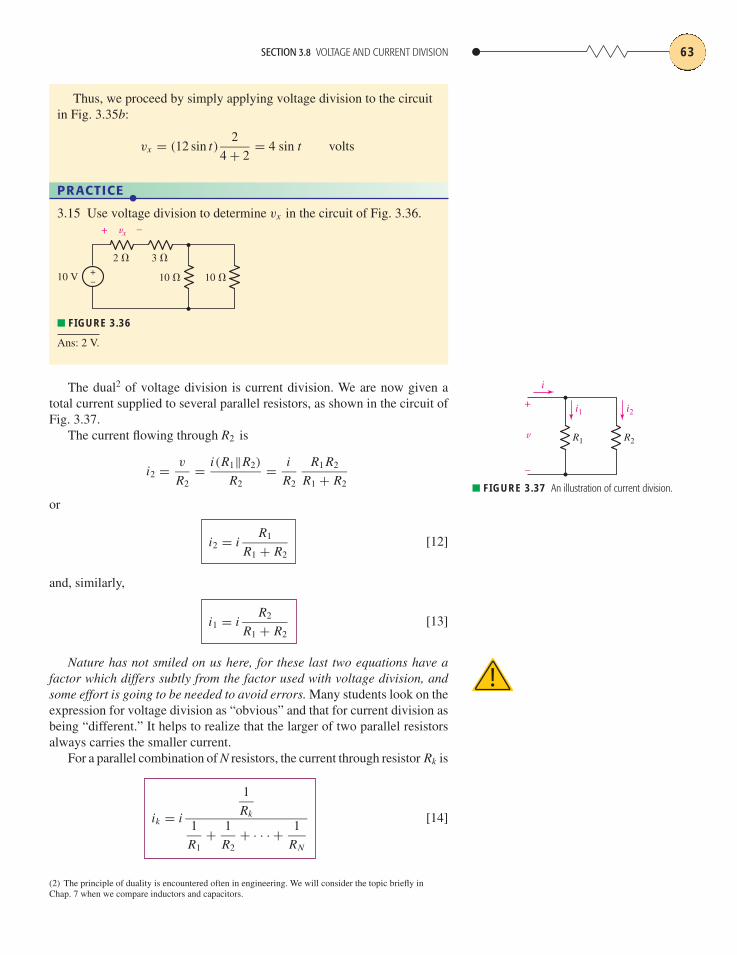
3.15 Use voltage division to determine vx in the circuit of Fig. 3.36.
Ans: 2 V.
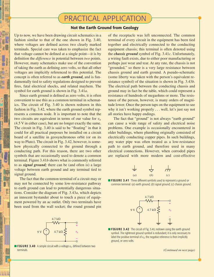
The dual2 of voltage division is current division. We are now given atotal current supplied to several parallel resistors, as shown in the circuit ofFig. 3.37.
The current flowing through R2 is
i2 = v
R2= i(R1‖R2)
R2= i
R2
R1 R2
R1 + R2
or
[12]
and, similarly,
[13]
Nature has not smiled on us here, for these last two equations have afactor which differs subtly from the factor used with voltage division, andsome effort is going to be needed to avoid errors. Many students look on theexpression for voltage division as “obvious” and that for current division asbeing “different.” It helps to realize that the larger of two parallel resistorsalways carries the smaller current.
For a parallel combination of N resistors, the current through resistor Rk is
[14]ik = i
1
Rk
1
R1+ 1
R2+ · · · + 1
RN
i1 = iR2
R1 + R2
i2 = iR1
R1 + R2
+–10 V
2 � 3 �
10 � 10 �
vx+ –
■ FIGURE 3.36
i
v
+
–
R2R1
i1 i2
■ FIGURE 3.37 An illustration of current division.
(2) The principle of duality is encountered often in engineering. We will consider the topic briefly inChap. 7 when we compare inductors and capacitors.

Written in terms of conductances,
ik = iGk
G1 + G2 + · · · + G N
which strongly resembles Eq. [11] for voltage division.
CHAPTER 3 VOLTAGE AND CURRENT LAWS64
EXAMPLE 3.14Write an expression for the current through the 3 � resistor in thecircuit of Fig. 3.38.
The total current flowing into the 3 �–6 � combination is
i(t) = 12 sin t
4 + 3‖6= 12 sin t
4 + 2= 2 sin t A
and thus the desired current is given by current division:
i3(t) = (2 sin t)
(6
6 + 3
)= 4
3sin t A
i3
vx
+
–
4 �
6 �12 sin t V 3 �+–
■ FIGURE 3.38 A circuit used as an example ofcurrent division. The wavy line in the voltage sourcesymbol indicates a sinusoidal variation with time.
Unfortunately, current division is sometimes applied when it is notapplicable. As one example, let us consider again the circuit shown inFig. 3.33c, a circuit that we have already agreed contains no circuit ele-ments that are in series or in parallel. Without parallel resistors, there is noway that current division can be applied. Even so, there are too many stu-dents who take a quick look at resistors RA and RB and try to apply currentdivision, writing an incorrect equation such as
iA = iSRB
RA + RB
Remember, parallel resistors must be branches between the same pair ofnodes.
PRACTICE ●
3.16 In the circuit of Fig. 3.39, use resistance combination methodsand current division to find i1, i2, and v3.
i1i2
v3
+
–
125 � 50 � 240 � 20 �
2 � 40 �
120 mA
■ FIGURE 3.39
Ans: 100 mA; 50 mA; 0.8 V.
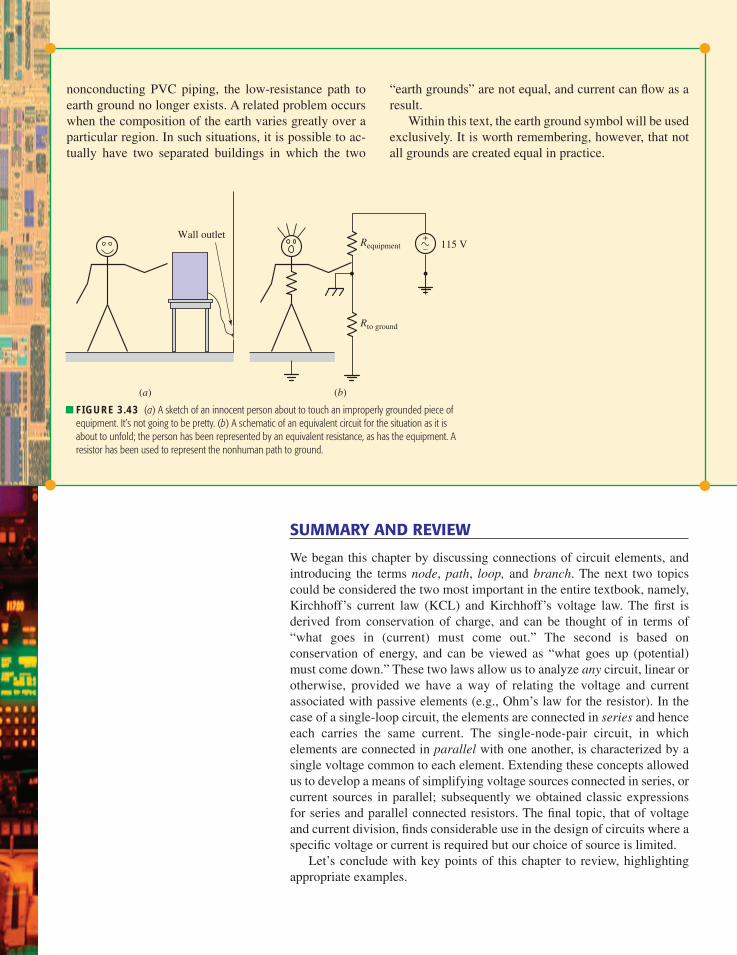
Up to now, we have been drawing circuit schematics in afashion similar to that of the one shown in Fig. 3.40,where voltages are defined across two clearly markedterminals. Special care was taken to emphasize the factthat voltage cannot be defined at a single point—it is bydefinition the difference in potential between two points.However, many schematics make use of the conventionof taking the earth as defining zero volts, so that all othervoltages are implicitly referenced to this potential. Theconcept is often referred to as earth ground, and is fun-damentally tied to safety regulations designed to preventfires, fatal electrical shocks, and related mayhem. Thesymbol for earth ground is shown in Fig. 3.41a.
Since earth ground is defined as zero volts, it is oftenconvenient to use this as a common terminal in schemat-ics. The circuit of Fig. 3.40 is shown redrawn in thisfashion in Fig. 3.42, where the earth ground symbol rep-resents a common node. It is important to note that thetwo circuits are equivalent in terms of our value for va
(4.5 V in either case), but are no longer exactly the same.The circuit in Fig. 3.40 is said to be “floating” in that itcould for all practical purposes be installed on a circuitboard of a satellite in geosynchronous orbit (or on itsway to Pluto). The circuit in Fig. 3.42, however, is some-how physically connected to the ground through aconducting path. For this reason, there are two othersymbols that are occasionally used to denote a commonterminal. Figure 3.41b shows what is commonly referredto as signal ground; there can be (and often is) a largevoltage between earth ground and any terminal tied tosignal ground.
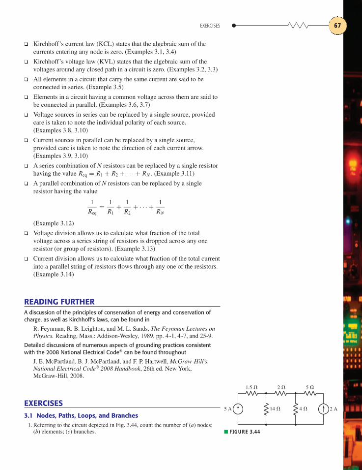
The fact that the common terminal of a circuit may ormay not be connected by some low-resistance pathwayto earth ground can lead to potentially dangerous situa-tions. Consider the diagram of Fig. 3.43a, which depictsan innocent bystander about to touch a piece of equip-ment powered by an ac outlet. Only two terminals havebeen used from the wall socket; the round ground pin
PRACTICAL APPLICATIONNot the Earth Ground from Geology
PRACTICAL APPLICATION
of the receptacle was left unconnected. The commonterminal of every circuit in the equipment has been tiedtogether and electrically connected to the conductingequipment chassis; this terminal is often denoted usingthe chassis ground symbol of Fig. 3.41c. Unfortunately,a wiring fault exists, due to either poor manufacturing orperhaps just wear and tear. At any rate, the chassis is not“grounded,” so there is a very large resistance betweenchassis ground and earth ground. A pseudo-schematic(some liberty was taken with the person’s equivalent re-sistance symbol) of the situation is shown in Fig. 3.43b.The electrical path between the conducting chassis andground may in fact be the table, which could represent aresistance of hundreds of megaohms or more. The resis-tance of the person, however, is many orders of magni-tude lower. Once the person taps on the equipment to seewhy it isn’t working properly . . . well, let’s just say notall stories have happy endings.
The fact that “ground” is not always “earth ground”can cause a wide range of safety and electrical noiseproblems. One example is occasionally encountered inolder buildings, where plumbing originally consisted ofelectrically conducting copper pipes. In such buildings,any water pipe was often treated as a low-resistancepath to earth ground, and therefore used in manyelectrical connections. However, when corroded pipesare replaced with more modern and cost-effective
+–9 V
4.7 k�
4.7 k� va
+
–
■ FIGURE 3.40 A simple circuit with a voltage va defined between twoterminals.
+–9 V
4.7 k�
4.7 k� va
+
–
■ FIGURE 3.42 The circuit of Fig. 3.40, redrawn using the earth groundsymbol. The rightmost ground symbol is redundant; it is only necessary tolabel the positive terminal of va; the negative reference is then implicitlyground, or zero volts.
(a) (b) (c)
■ FIGURE 3.41 Three different symbols used to represent a ground orcommon terminal: (a) earth ground; (b) signal ground; (c) chassis ground.
(Continued on next page)
nonconducting PVC piping, the low-resistance path toearth ground no longer exists. A related problem occurswhen the composition of the earth varies greatly over aparticular region. In such situations, it is possible to ac-tually have two separated buildings in which the two
“earth grounds” are not equal, and current can flow as aresult.
Within this text, the earth ground symbol will be usedexclusively. It is worth remembering, however, that notall grounds are created equal in practice.
(a)
Wall outletRequipment
Rto ground
(b)
115 V+–
■ FIGURE 3.43 (a) A sketch of an innocent person about to touch an improperly grounded piece ofequipment. It’s not going to be pretty. (b) A schematic of an equivalent circuit for the situation as it isabout to unfold; the person has been represented by an equivalent resistance, as has the equipment. Aresistor has been used to represent the nonhuman path to ground.
SUMMARY AND REVIEW
We began this chapter by discussing connections of circuit elements, andintroducing the terms node, path, loop, and branch. The next two topicscould be considered the two most important in the entire textbook, namely,Kirchhoff’s current law (KCL) and Kirchhoff’s voltage law. The first isderived from conservation of charge, and can be thought of in terms of“what goes in (current) must come out.” The second is based onconservation of energy, and can be viewed as “what goes up (potential)must come down.” These two laws allow us to analyze any circuit, linear orotherwise, provided we have a way of relating the voltage and currentassociated with passive elements (e.g., Ohm’s law for the resistor). In thecase of a single-loop circuit, the elements are connected in series and henceeach carries the same current. The single-node-pair circuit, in whichelements are connected in parallel with one another, is characterized by asingle voltage common to each element. Extending these concepts allowedus to develop a means of simplifying voltage sources connected in series, orcurrent sources in parallel; subsequently we obtained classic expressionsfor series and parallel connected resistors. The final topic, that of voltageand current division, finds considerable use in the design of circuits where aspecific voltage or current is required but our choice of source is limited.
Let’s conclude with key points of this chapter to review, highlightingappropriate examples.
EXERCISES 6767
❑ Kirchhoff’s current law (KCL) states that the algebraic sum of thecurrents entering any node is zero. (Examples 3.1, 3.4)
❑ Kirchhoff’s voltage law (KVL) states that the algebraic sum of thevoltages around any closed path in a circuit is zero. (Examples 3.2, 3.3)
❑ All elements in a circuit that carry the same current are said to beconnected in series. (Example 3.5)
❑ Elements in a circuit having a common voltage across them are said tobe connected in parallel. (Examples 3.6, 3.7)
❑ Voltage sources in series can be replaced by a single source, providedcare is taken to note the individual polarity of each source. (Examples 3.8, 3.10)
❑ Current sources in parallel can be replaced by a single source, provided care is taken to note the direction of each current arrow.(Examples 3.9, 3.10)
❑ A series combination of N resistors can be replaced by a single resistorhaving the value Req = R1 + R2 + · · · + RN . (Example 3.11)
❑ A parallel combination of N resistors can be replaced by a singleresistor having the value
1
Req= 1
R1+ 1
R2+ · · · + 1
RN
(Example 3.12)
❑ Voltage division allows us to calculate what fraction of the totalvoltage across a series string of resistors is dropped across any oneresistor (or group of resistors). (Example 3.13)
❑ Current division allows us to calculate what fraction of the total currentinto a parallel string of resistors flows through any one of the resistors.(Example 3.14)
READING FURTHERA discussion of the principles of conservation of energy and conservation ofcharge, as well as Kirchhoff’s laws, can be found in
R. Feynman, R. B. Leighton, and M. L. Sands, The Feynman Lectures onPhysics. Reading, Mass.: Addison-Wesley, 1989, pp. 4-1, 4-7, and 25-9.
Detailed discussions of numerous aspects of grounding practices consistentwith the 2008 National Electrical Code® can be found throughout
J. E. McPartland, B. J. McPartland, and F. P. Hartwell, McGraw-Hill’sNational Electrical Code® 2008 Handbook, 26th ed. New York, McGraw-Hill, 2008.
EXERCISES3.1 Nodes, Paths, Loops, and Branches
1. Referring to the circuit depicted in Fig. 3.44, count the number of (a) nodes;(b) elements; (c) branches.
4 � 2 A5 A 14 �
1.5 � 2 � 5 �
■ FIGURE 3.44
CHAPTER 3 VOLTAGE AND CURRENT LAWS68
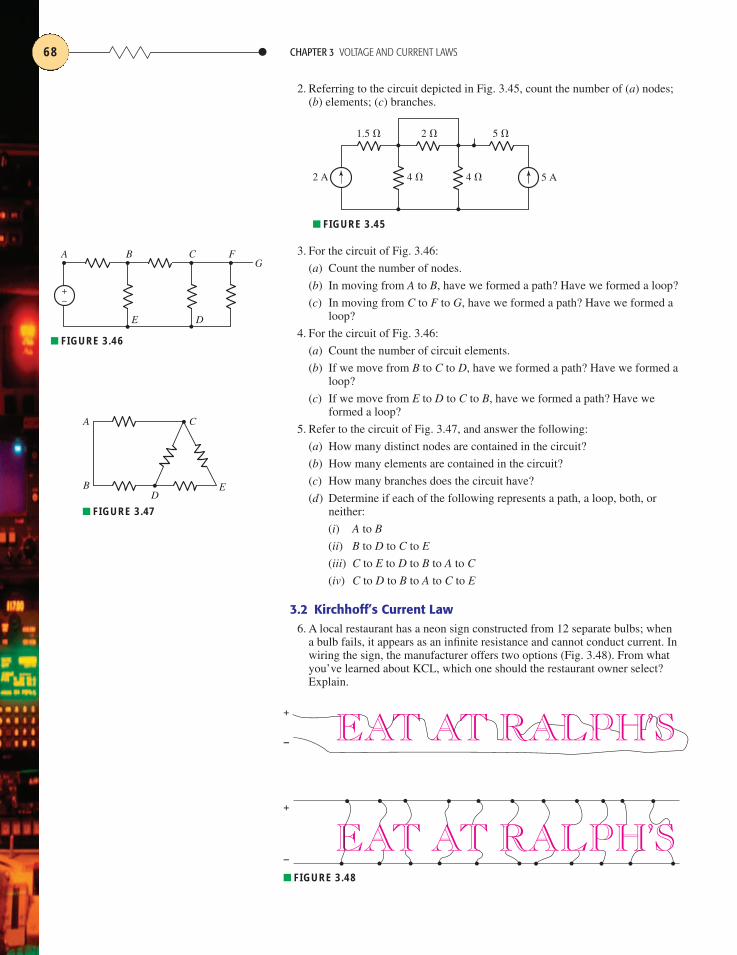
2. Referring to the circuit depicted in Fig. 3.45, count the number of (a) nodes;(b) elements; (c) branches.
+–
A B C FG
E D
■ FIGURE 3.46
CA
B ED
■ FIGURE 3.47
4 � 5 A2 A 4 �
1.5 � 2 � 5 �
■ FIGURE 3.45
EAT AT RALPH’S
EAT AT RALPH’S
+
–
+
–
■ FIGURE 3.48
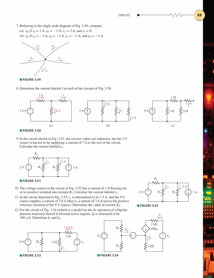
3. For the circuit of Fig. 3.46:
(a) Count the number of nodes.
(b) In moving from A to B, have we formed a path? Have we formed a loop?
(c) In moving from C to F to G, have we formed a path? Have we formed aloop?
4. For the circuit of Fig. 3.46:
(a) Count the number of circuit elements.
(b) If we move from B to C to D, have we formed a path? Have we formed aloop?
(c) If we move from E to D to C to B, have we formed a path? Have weformed a loop?
5. Refer to the circuit of Fig. 3.47, and answer the following:
(a) How many distinct nodes are contained in the circuit?
(b) How many elements are contained in the circuit?
(c) How many branches does the circuit have?
(d) Determine if each of the following represents a path, a loop, both, orneither:
(i) A to B
(ii) B to D to C to E
(iii) C to E to D to B to A to C
(iv) C to D to B to A to C to E
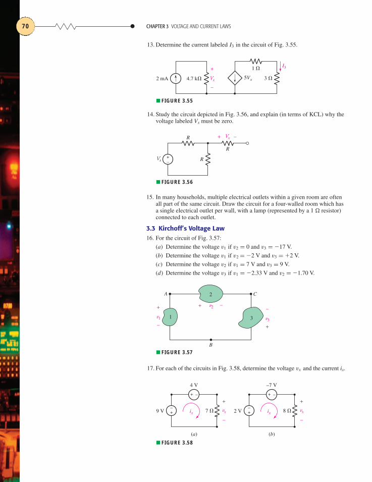
3.2 Kirchhoff’s Current Law6. A local restaurant has a neon sign constructed from 12 separate bulbs; when
a bulb fails, it appears as an infinite resistance and cannot conduct current. Inwiring the sign, the manufacturer offers two options (Fig. 3.48). From whatyou’ve learned about KCL, which one should the restaurant owner select?Explain.
EXERCISES 6969
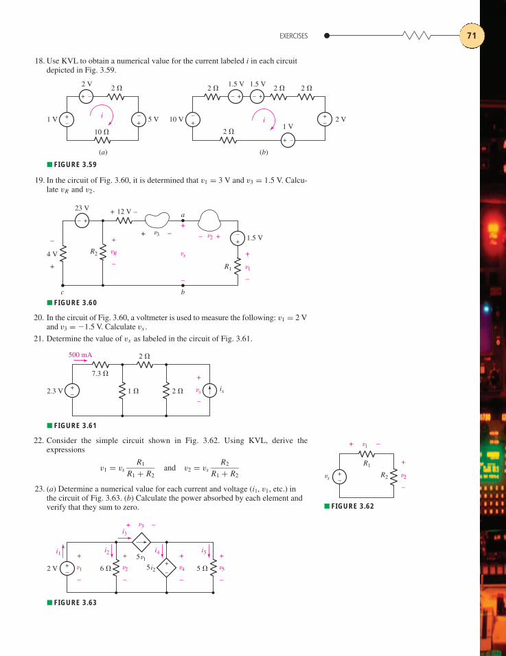
7. Referring to the single node diagram of Fig. 3.49, compute:
(a) iB, if iA = 1 A, iD = �2 A, iC = 3 A, and iE = 0;
(b) iE, if iA = �1 A, iB = �1 A, iC = �1 A, and iD = �1 A.
iC
iBiA
iD
iE
■ FIGURE 3.49
+–
6 A1.5 V
7 A I
I3 A
3 A
I2 A 9 A
(a) (b) (c)
1 �
1 � 5 �
■ FIGURE 3.50
+–
R2 R3
R1
3 A2 V
1 Ai2
■ FIGURE 3.51
8. Determine the current labeled I in each of the circuits of Fig. 3.50.
9. In the circuit shown in Fig. 3.51, the resistor values are unknown, but the 2 Vsource is known to be supplying a current of 7 A to the rest of the circuit.Calculate the current labeled i2.
+–
R2 R3
R1
7 A– 2 V
–3 Ai2
■ FIGURE 3.52
RA 6 �
5 �+–
+–
ix
–1.6 A
9 V vx
■ FIGURE 3.53
+–
+–
+ –V1 V2
R1
R2 1 k�
1 k�
150IBIB
IE
IC
■ FIGURE 3.54
10. The voltage source in the circuit of Fig. 3.52 has a current of 1 A flowing outof its positive terminal into resistor R1. Calculate the current labeled i2.
11. In the circuit depicted in Fig. 3.53, ix is determined to be 1.5 A, and the 9 Vsource supplies a current of 7.6 A (that is, a current of 7.6 A leaves the positivereference terminal of the 9 V source). Determine the value of resistor RA.
12. For the circuit of Fig. 3.54 (which is a model for the dc operation of a bipolarjunction transistor biased in forward active region), IB is measured to be100 μA. Determine IC and IE.
CHAPTER 3 VOLTAGE AND CURRENT LAWS70
Vs+–
R
R
R
Vx+ –
■ FIGURE 3.56
v1
+
–v3
–
+
v2+ –
A C
B
1
2
3
■ FIGURE 3.57
13. Determine the current labeled I3 in the circuit of Fig. 3.55.
2 mA 4.7 k� 3 �
1 �
5VxVx
+
–
I3
■ FIGURE 3.55
14. Study the circuit depicted in Fig. 3.56, and explain (in terms of KCL) why thevoltage labeled Vx must be zero.
15. In many households, multiple electrical outlets within a given room are oftenall part of the same circuit. Draw the circuit for a four-walled room which hasa single electrical outlet per wall, with a lamp (represented by a 1 � resistor)connected to each outlet.
3.3 Kirchoff’s Voltage Law16. For the circuit of Fig. 3.57:
(a) Determine the voltage v1 if v2 = 0 and v3 = �17 V.
(b) Determine the voltage v1 if v2 = �2 V and v3 = �2 V.
(c) Determine the voltage v2 if v1 = 7 V and v3 = 9 V.
(d) Determine the voltage v3 if v1 = �2.33 V and v2 = �1.70 V.
17. For each of the circuits in Fig. 3.58, determine the voltage vx and the current ix.
–+
–+
9 V
4 V
7 � vx
+
–
ix–+
–+
2 V
–7 V
8 � vx
+
–
ix
(a) (b)
■ FIGURE 3.58
EXERCISES 71
+– +
–
+ –
1 V
2 V
5 V
2 �
10 �
(a)
i +–+
–
+ –
+–
10 V
1.5 V
+–
1.5 V
2 V
2 �
2 �1 V
2 � 2 �
(b)
i
■ FIGURE 3.59
+–
+–
4 V
–
+
vx
+
–
vR
–
+
v1
+
–
v2 +–
+ –12 V
+ –v3
R1
R2
1.5 V
bc
a23 V
■ FIGURE 3.60
18. Use KVL to obtain a numerical value for the current labeled i in each circuitdepicted in Fig. 3.59.
19. In the circuit of Fig. 3.60, it is determined that v1 = 3 V and v3 = 1.5 V. Calcu-late vR and v2.
20. In the circuit of Fig. 3.60, a voltmeter is used to measure the following: v1 = 2 Vand v3 = �1.5 V. Calculate vx .
21. Determine the value of vx as labeled in the circuit of Fig. 3.61.
+–
vx
2 �
7.3 �
2 �1 �2.3 V ix
+
–
500 mA
■ FIGURE 3.61
22. Consider the simple circuit shown in Fig. 3.62. Using KVL, derive theexpressions
v1 = vsR1
R1 + R2and v2 = vs
R2
R1 + R2
23. (a) Determine a numerical value for each current and voltage (i1, v1, etc.) inthe circuit of Fig. 3.63. (b) Calculate the power absorbed by each element andverify that they sum to zero.
+–
R2
R1
vs v2
+
–
v1+ –
■ FIGURE 3.62
5i2
5v1
5 �6 �2 V v1
+
–
v2
+
–
v4
+
–
v5
+
–
v3+ –
i4i2 i5
+–
+
–
i1
i3
■ FIGURE 3.63
CHAPTER 3 VOLTAGE AND CURRENT LAWS72
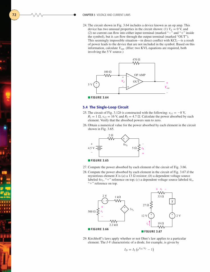
24. The circuit shown in Fig. 3.64 includes a device known as an op amp. Thisdevice has two unusual properties in the circuit shown: (1) Vd = 0 V, and(2) no current can flow into either input terminal (marked “−” and “+” insidethe symbol), but it can flow through the output terminal (marked “OUT”).This seemingly impossible situation—in direct conflict with KCL—is a resultof power leads to the device that are not included in the symbol. Based on thisinformation, calculate Vout. (Hint: two KVL equations are required, bothinvolving the 5 V source.)
1 k�
2.2 k�
500 �
+–
– +
2 V
3vxvx
+
–
■ FIGURE 3.66
+–
+–
ix
X27 �
33 �
19 �
2 V12 V
v1+ –
■ FIGURE 3.67
+–5 V
Vd
+
– Vout
+
–
100 �
470 �
OP AMP
OUT
+
–
■ FIGURE 3.64
3.4 The Single-Loop Circuit25. The circuit of Fig. 3.12b is constructed with the following: vs1 = �8 V,
R1 = 1 �, vs2 = 16 V, and R2 = 4.7 �. Calculate the power absorbed by eachelement. Verify that the absorbed powers sum to zero.
26. Obtain a numerical value for the power absorbed by each element in the circuitshown in Fig. 3.65.
8vA
2 �
5 �
+ –
4.5 V+
–vA
–
+
■ FIGURE 3.65
27. Compute the power absorbed by each element of the circuit of Fig. 3.66.
28. Compute the power absorbed by each element in the circuit of Fig. 3.67 if themysterious element X is (a) a 13 � resistor; (b) a dependent voltage sourcelabeled 4v1, “�” reference on top; (c) a dependent voltage source labeled 4ix,“�” reference on top.
29. Kirchhoff’s laws apply whether or not Ohm’s law applies to a particularelement. The I-V characteristic of a diode, for example, is given by
ID = IS(eVD/VT − 1
)
EXERCISES 73
where VT = 27 mV at room temperature and IS can vary from 10−12 to 10−3 A. In the circuit of Fig. 3.68, use KVL/KCL to obtain VD if IS = 29 pA.(Note: This problem results in a transcendental equation, requiring an iterativeapproach to obtaining a numerical solution. Most scientific calculators willperform such a function.)
3.5 The Single-Node-Pair Circuit30. Referring to the circuit of Fig. 3.69, (a) determine the two currents i1 and i2;
(b) compute the power absorbed by each element.
+–
100 �
3 V ID VD
+
–
■ FIGURE 3.68
3 A 7 A 2 �R1 R2v
+
– i1 i2
4 �
■ FIGURE 3.69
–2 A 3 A 6 �R1 R2v
+
– i1 i2
10 �
■ FIGURE 3.70
1 A 2 A5 � 5 Av
+
–5 �
■ FIGURE 3.71
3 �3ix1 � 2 Av
+
–
ix
■ FIGURE 3.72
2.8 k�
4.7 k�
1 k�
5 mA
3 mA
■ FIGURE 3.73
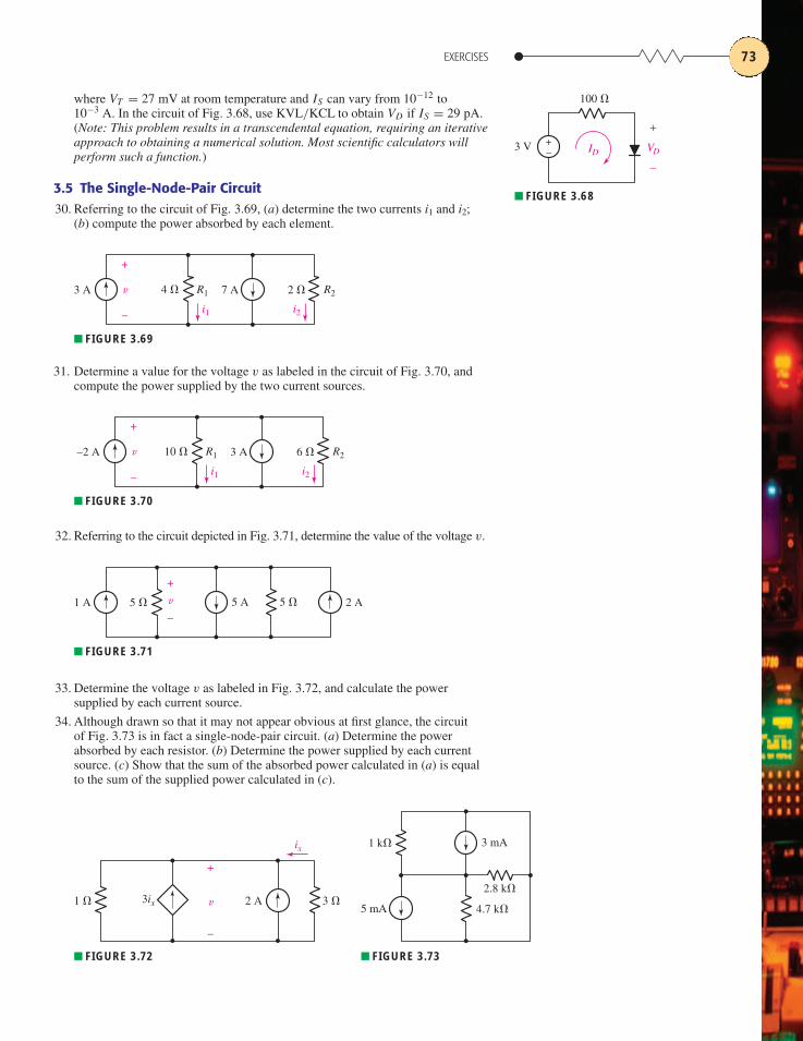
31. Determine a value for the voltage v as labeled in the circuit of Fig. 3.70, andcompute the power supplied by the two current sources.
32. Referring to the circuit depicted in Fig. 3.71, determine the value of the voltage v.
33. Determine the voltage v as labeled in Fig. 3.72, and calculate the powersupplied by each current source.
34. Although drawn so that it may not appear obvious at first glance, the circuitof Fig. 3.73 is in fact a single-node-pair circuit. (a) Determine the powerabsorbed by each resistor. (b) Determine the power supplied by each currentsource. (c) Show that the sum of the absorbed power calculated in (a) is equalto the sum of the supplied power calculated in (c).

41. (a) Determine the values for IX and VY in the circuit shown in Fig. 3.79.(b) Are those values necessarily unique for that circuit? Explain. (c) Simplifythe circuit of Fig. 3.79 as much as possible and still maintain the values for vand i. (Your circuit must contain the 1 � resistor.)
CHAPTER 3 VOLTAGE AND CURRENT LAWS74
3.6 Series and Parallel Connected Sources35. Determine the numerical value for veq in Fig. 3.74a, if (a) v1 = 0, v2 = �3 V,
and v3 = �3 V; (b) v1 = v2 = v3 = 1 V; (c) v1 = �9 V, v2 = 4.5 V, v3 = 1 V.
36. Determine the numerical value for ieq in Fig. 3.74b, if (a) i1 = 0, i2 = �3 A,and i3 = �3 A; (b) i1 = i2 = i3 = 1 A; (c) i1 = �9 A, i2 = 4.5 A, i3 = 1 A.
37. For the circuit presented in Fig. 3.75, determine the current labeled i by firstcombining the four sources into a single equivalent source.
38. Determine the value of v1 required to obtain a zero value for the current la-beled i in the circuit of Fig. 3.76.
7 A 8 A2 � 5 Av
+
–3 �
■ FIGURE 3.77
=
(a)
v1
v2
v3
+–
+– veq
+–
+–
=
(b)
i1 i2 i3 ieq
■ FIGURE 3.74
–+
+–
6 V
2 V
12 V 2 V
–+
1 k�
+–
i
■ FIGURE 3.75
–+
–+
4 V
v1
2 V 1 V
+–
7 �
7 �+–
i
■ FIGURE 3.76
1.28 A –2.57 A1 � ISv
+
–1 �
■ FIGURE 3.78
–3 A 3 A
IX 3 V–4 A 1 �v
+
– i
+–
4 V+–
VY+–
■ FIGURE 3.79
39. (a) For the circuit of Fig. 3.77, determine the value for the voltage labeled v,after first simplifying the circuit to a single current source in parallel with two resistors. (b) Verify that the power supplied by your equivalent source is equal tothe sum of the supplied powers of the individual sources in the original circuit.
40. What value of IS in the circuit of Fig. 3.78 will result in a zero voltage v?
EXERCISES 75
2 �
2 �3 �
1 �
1 �
2 �
4 �
(a) (b)
■ FIGURE 3.80
+–
+–
2 � 7 �
1 �
5 �
1 V3 V
i
■ FIGURE 3.82
2 �
1 �
4 �
(a)
1 � 4 � 3 �
(b)
■ FIGURE 3.81
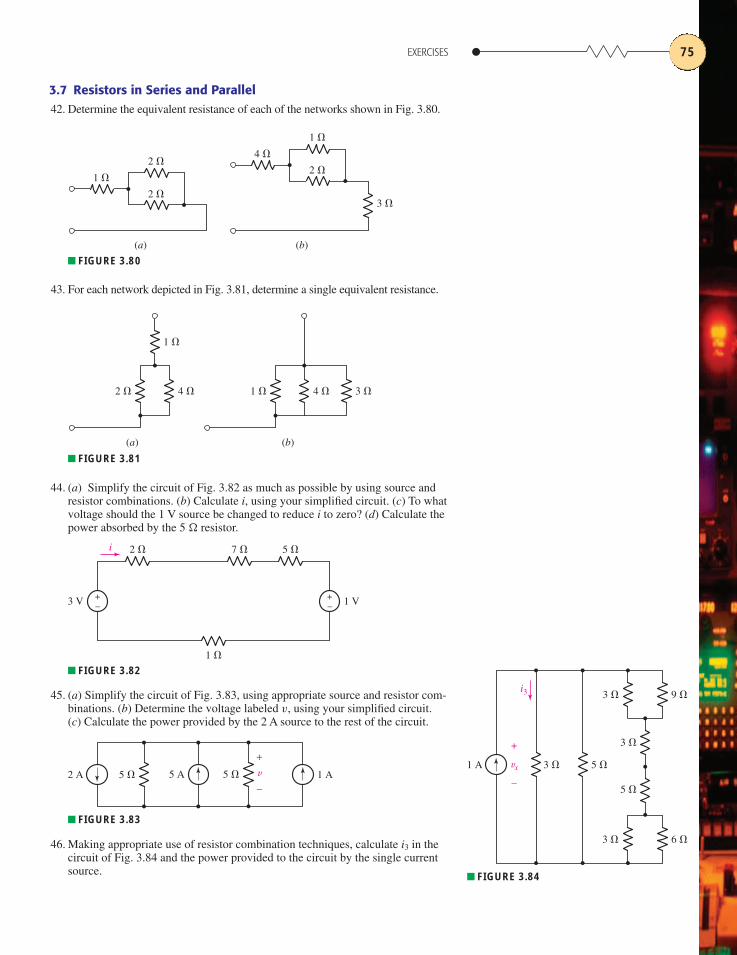
3.7 Resistors in Series and Parallel42. Determine the equivalent resistance of each of the networks shown in Fig. 3.80.
43. For each network depicted in Fig. 3.81, determine a single equivalent resistance.
44. (a) Simplify the circuit of Fig. 3.82 as much as possible by using source andresistor combinations. (b) Calculate i, using your simplified circuit. (c) To whatvoltage should the 1 V source be changed to reduce i to zero? (d) Calculate thepower absorbed by the 5 � resistor.
45. (a) Simplify the circuit of Fig. 3.83, using appropriate source and resistor com-binations. (b) Determine the voltage labeled v, using your simplified circuit. (c) Calculate the power provided by the 2 A source to the rest of the circuit.
2 A 1 A5 � 5 A v
+
–5 �
■ FIGURE 3.83
46. Making appropriate use of resistor combination techniques, calculate i3 in thecircuit of Fig. 3.84 and the power provided to the circuit by the single currentsource.
3 � 5 �
6 �3 �
1 A
9 �3 �
5 �
3 �
vx
+
–
i3
■ FIGURE 3.84
CHAPTER 3 VOLTAGE AND CURRENT LAWS76
4 A 2i
6 �
15 �3�
6 � 9 A6 �3 A
i
■ FIGURE 3.86
49. Calculate the equivalent resistance Req of the network shown in Fig. 3.87 if R1 = 2R2 = 3R3 = 4R4 etc. and R11 = 3 �.
Req
R2 R5 R8
R3
R1 R4 R7 R10 R11
R6 R9
■ FIGURE 3.87
i
v2
+
–
v1+ –
v
+
–
R1
R2
■ FIGURE 3.88
i
v
+
–
R2R1
i1 i2
■ FIGURE 3.89
3 � 15 �
6 �6 �
2 A 4i
9 �
vx
+
–
i
■ FIGURE 3.85
47. Calculate the voltage labeled vx in the circuit of Fig. 3.85 after first simplify-ing, using appropriate source and resistor combinations.
48. Determine the power absorbed by the 15 � resistor in the circuit of Fig. 3.86.
50. Show how to combine four 100 � resistors to obtain an equivalent resistanceof (a) 25 �; (b) 60 �; (c) 40 �.
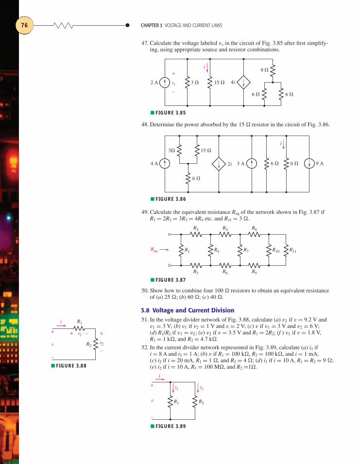
3.8 Voltage and Current Division51. In the voltage divider network of Fig. 3.88, calculate (a) v2 if v = 9.2 V and
v1 = 3 V; (b) v1 if v2 = 1 V and v = 2 V; (c) v if v1 = 3 V and v2 = 6 V; (d) R1/R2 if v1 = v2; (e) v2 if v = 3.5 V and R1 = 2R2; (f ) v1 if v = 1.8 V, R1 = 1 k�, and R2 = 4.7 k�.
52. In the current divider network represented in Fig. 3.89, calculate (a) i1 if i = 8 A and i2 = 1 A; (b) v if R1 = 100 k�, R2 = 100 k�, and i = 1 mA; (c) i2 if i = 20 mA, R1 = 1 �, and R2 = 4 �; (d) i1 if i = 10 A, R1 = R2 = 9 �;(e) i2 if i = 10 A, R1 = 100 M�, and R2 =1�.
EXERCISES 77
+–3 V
2 � 3 �
2 � 10 �
vx+ –
■ FIGURE 3.91
v
+
–
R4R1
i1 i4
R2
i2
R3
i3
■ FIGURE 3.90
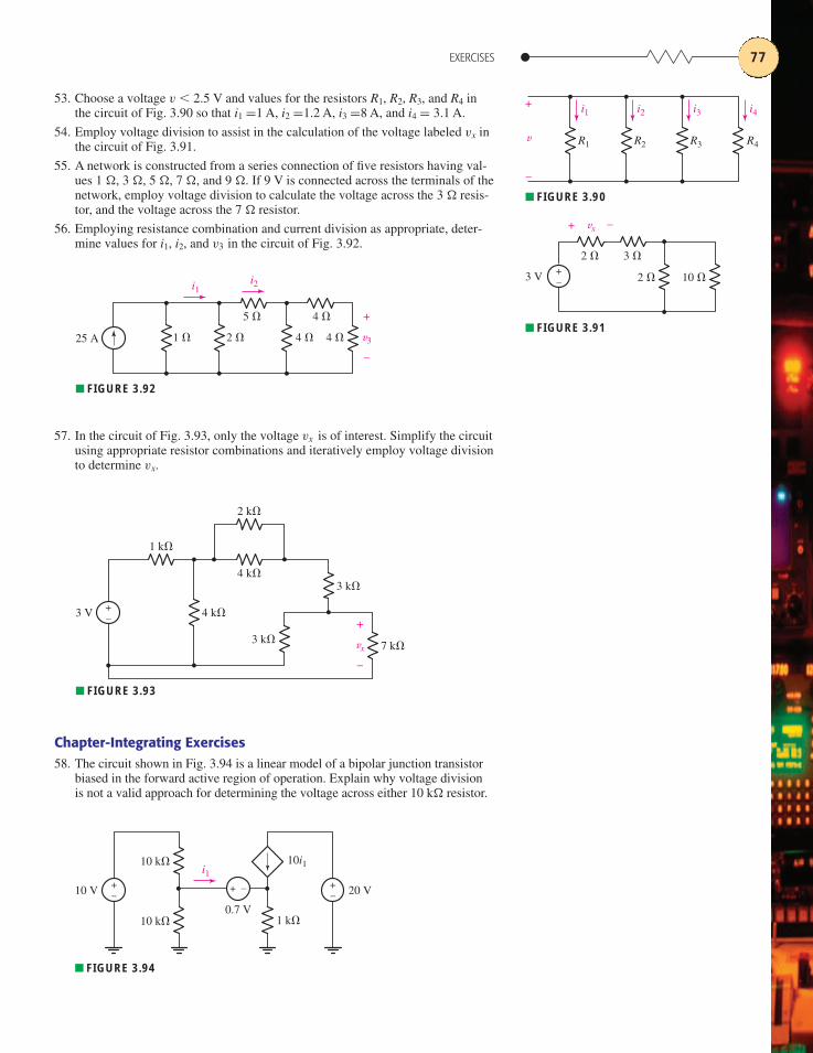
53. Choose a voltage v � 2.5 V and values for the resistors R1, R2, R3, and R4 inthe circuit of Fig. 3.90 so that i1 =1 A, i2 =1.2 A, i3 =8 A, and i4 = 3.1 A.
54. Employ voltage division to assist in the calculation of the voltage labeled vx inthe circuit of Fig. 3.91.
55. A network is constructed from a series connection of five resistors having val-ues 1 �, 3 �, 5 �, 7 �, and 9 �. If 9 V is connected across the terminals of thenetwork, employ voltage division to calculate the voltage across the 3 � resis-tor, and the voltage across the 7 � resistor.
56. Employing resistance combination and current division as appropriate, deter-mine values for i1, i2, and v3 in the circuit of Fig. 3.92.
v3
+
–
1 � 2 �
5 � 4 �
4 � 4 �25 A
i1i2
■ FIGURE 3.92
57. In the circuit of Fig. 3.93, only the voltage vx is of interest. Simplify the circuitusing appropriate resistor combinations and iteratively employ voltage divisionto determine vx.
2 k�
4 k�3 k�
7 k�
4 k�
3 k�
3 V +–
1 k�
vx
+
–
■ FIGURE 3.93
+–
+–
+ –10 V 20 V
0.7 V
10 k�
10 k� 1 k�
10i1i1
■ FIGURE 3.94
Chapter-Integrating Exercises58. The circuit shown in Fig. 3.94 is a linear model of a bipolar junction transistor
biased in the forward active region of operation. Explain why voltage divisionis not a valid approach for determining the voltage across either 10 k� resistor.
CHAPTER 3 VOLTAGE AND CURRENT LAWS78
10 � 10 � 50 � 4 �
40 �20 � 20 �
2 V +–
■ FIGURE 3.97
1 �
2 �2 �
5 �
5 �
2 A
2 �
■ FIGURE 3.98
6 cos 2300t �V
1 k�
3 k� 3.3 k�15 k� gmv�v�
+
–
vout
+
–
+–
■ FIGURE 3.96
12 cos 1000t mV
30 �
15 k� 1 k�10 k�gmv�v�
+
–
vout
+
–
+–
■ FIGURE 3.95
61. With regard to the circuit shown in Fig. 3.97, compute (a) the voltage acrossthe two 10 � resistors, assuming the top terminal is the positive reference; (b) the power dissipated by the 4 � resistor.
59. A common midfrequency model for a field effect–based amplifier circuit isshown in Fig. 3.95. If the controlling parameter gm (known as the transconduc-tance) is equal to 1.2 mS, employ current division to obtain the current throughthe 1 k� resistor, and then calculate the amplifier output voltage vout.
60. The circuit depicted in Fig. 3.96 is routinely employed to model the midfre-quency operation of a bipolar junction transistor–based amplifier. Calculate theamplifier output vout if the transconductance gm is equal to 322 mS.
62. Delete the leftmost 10 � resistor in the circuit of Fig. 3.97, and compute (a) the current flowing into the left-hand terminal of the 40 � resistor; (b) thepower supplied by the 2 V source; (c) the power dissipated by the 4 �resistor.
63. Consider the seven-element circuit depicted in Fig. 3.98. (a) How many nodes,loops, and branches does it contain? (b) Calculate the current flowing througheach resistor. (c) Determine the voltage across the current source, assuming thetop terminal is the positive reference terminal.


