
VOICE SWITCHED SPEAKERPHONE CIRCUITradiocom.dn.ua/image/data/pdf/MC33219A_MOT.pdf · The Motorola...
28
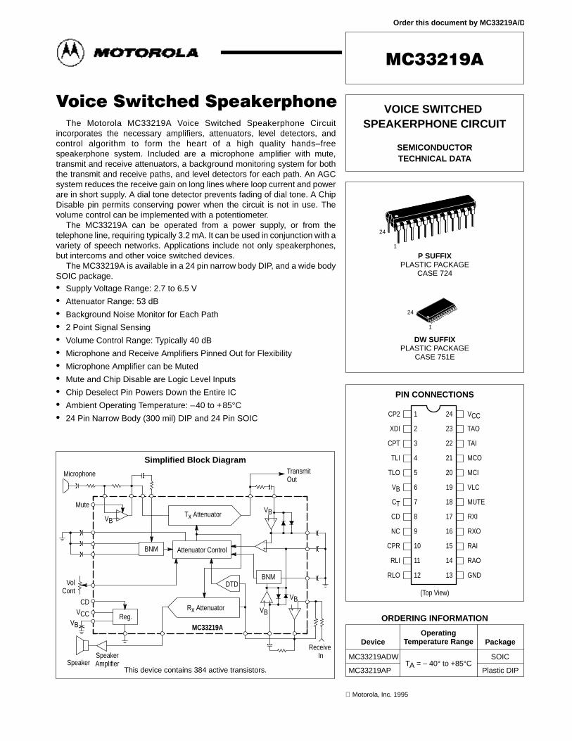
Order this document by MC33219A/D Device Operating Temperature Range Package SEMICONDUCTOR TECHNICAL DATA DW SUFFIX PLASTIC PACKAGE CASE 751E VOICE SWITCHED SPEAKERPHONE CIRCUIT PIN CONNECTIONS ORDERING INFORMATION MC33219ADW MC33219AP T A = – 40° to +85°C SOIC Plastic DIP 24 1 P SUFFIX PLASTIC PACKAGE CASE 724 24 1 CP2 1 24 (Top View) V CC 2 3 4 5 6 7 8 9 10 11 12 23 22 21 20 19 18 17 16 15 14 13 XDI CPT TLI TLO V B C T CD NC CPR RLI RLO TAO TAI MCO MCI VLC MUTE RXI RXO RAI RAO GND Simplified Block Diagram This device contains 384 active transistors. Microphone Transmit Out Mute Vol Cont V B V B V B V B V B BNM Reg. R x Attenuator MC33219A V CC T x Attenuator Attenuator Control DTD Speaker Amplifier Speaker CD Receive In BNM The Motorola MC33219A Voice Switched Speakerphone Circuit incorporates the necessary amplifiers, attenuators, level detectors, and control algorithm to form the heart of a high quality hands–free speakerphone system. Included are a microphone amplifier with mute, transmit and receive attenuators, a background monitoring system for both the transmit and receive paths, and level detectors for each path. An AGC system reduces the receive gain on long lines where loop current and power are in short supply. A dial tone detector prevents fading of dial tone. A Chip Disable pin permits conserving power when the circuit is not in use. The volume control can be implemented with a potentiometer. The MC33219A can be operated from a power supply, or from the telephone line, requiring typically 3.2 mA. It can be used in conjunction with a variety of speech networks. Applications include not only speakerphones, but intercoms and other voice switched devices. The MC33219A is available in a 24 pin narrow body DIP, and a wide body SOIC package. • Supply Voltage Range: 2.7 to 6.5 V • Attenuator Range: 53 dB • Background Noise Monitor for Each Path • 2 Point Signal Sensing • Volume Control Range: Typically 40 dB • Microphone and Receive Amplifiers Pinned Out for Flexibility • Microphone Amplifier can be Muted • Mute and Chip Disable are Logic Level Inputs • Chip Deselect Pin Powers Down the Entire IC • Ambient Operating Temperature: –40 to + 85°C • 24 Pin Narrow Body (300 mil) DIP and 24 Pin SOIC Motorola, Inc. 1995
Transcript of VOICE SWITCHED SPEAKERPHONE CIRCUITradiocom.dn.ua/image/data/pdf/MC33219A_MOT.pdf · The Motorola...
Order this document by MC33219A/D
DeviceOperating
Temperature Range Package
SEMICONDUCTORTECHNICAL DATA
DW SUFFIXPLASTIC PACKAGE
CASE 751E
VOICE SWITCHED SPEAKERPHONE CIRCUIT
PIN CONNECTIONS
ORDERING INFORMATION
MC33219ADW
MC33219APTA = – 40° to +85°C
SOIC
Plastic DIP
24
1
P SUFFIXPLASTIC PACKAGE
CASE 724
24
1
CP2 1 24
(Top View)
VCC
2
3
4
5
6
7
8
9
10
11
12
23
22
21
20
19
18
17
16
15
14
13
XDI
CPT
TLI
TLO
VB
CT
CD
NC
CPR
RLI
RLO
TAO
TAI
MCO
MCI
VLC
MUTE
RXI
RXO
RAI
RAO
GND
Simplified Block Diagram
This device contains 384 active transistors.
Microphone TransmitOut
Mute
VolCont
VBVB
VB
VB
VB
BNM
Reg.Rx Attenuator
MC33219A
VCC
Tx Attenuator
Attenuator Control
DTD
SpeakerAmplifierSpeaker
CD
Receive In
BNM
1MOTOROLA ANALOG IC DEVICE DATA
The Motorola MC33219A Voice Switched Speakerphone Circuit
incorporates the necessary amplifiers, attenuators, level detectors, andcontrol algorithm to form the heart of a high quality hands–freespeakerphone system. Included are a microphone amplifier with mute,transmit and receive attenuators, a background monitoring system for boththe transmit and receive paths, and level detectors for each path. An AGCsystem reduces the receive gain on long lines where loop current and powerare in short supply. A dial tone detector prevents fading of dial tone. A ChipDisable pin permits conserving power when the circuit is not in use. Thevolume control can be implemented with a potentiometer.
The MC33219A can be operated from a power supply, or from thetelephone line, requiring typically 3.2 mA. It can be used in conjunction with avariety of speech networks. Applications include not only speakerphones,but intercoms and other voice switched devices.
The MC33219A is available in a 24 pin narrow body DIP, and a wide bodySOIC package.
• Supply Voltage Range: 2.7 to 6.5 V
• Attenuator Range: 53 dB
• Background Noise Monitor for Each Path
• 2 Point Signal Sensing
• Volume Control Range: Typically 40 dB
• Microphone and Receive Amplifiers Pinned Out for Flexibility
• Microphone Amplifier can be Muted
• Mute and Chip Disable are Logic Level Inputs
• Chip Deselect Pin Powers Down the Entire IC
• Ambient Operating Temperature: –40 to +85°C• 24 Pin Narrow Body (300 mil) DIP and 24 Pin SOIC
Motorola, Inc. 1995

MC33219A
2 MOTOROLA ANALOG IC DEVICE DATA
MAXIMUM RATINGS
Rating Symbol Min Max Unit
Supply Voltage VCC –0.5 7.0 Vdc
Any Input Vin –0.4 VCC + 0.4 Vdc
Maximum Junction Temperature TJ – +150 °C
Storage Temperature Range Tstg –65 +150 °C
NOTE: Devices should not be operated at or outside these values. The “Recommended OperatingConditions” provide for actual device operation.
RECOMMENDED OPERATING CONDITIONS
Characteristic Symbol Min Typ Max Unit
Supply Voltage (Non–AGC Range) VCC 3.5 – 6.5 Vdc(AGC Range) 2.7 – 3.5
Maximum Attenuator Input Signal Vin(max) – – 300 mVrms
Volume Control Input (Pin 19) VINVLC VB – 1.1 – VB Vdc
Logic Input Voltage (Pins 8, 18) VINL VdcLow 0 – 0.8High 2.0 – VCC
Operating Temperature Range TA –40 – 85 °C
VB Output Current (VCC = 5.0 V) IVB – SeeFigure 12
– mA
ELECTRICAL CHARACTERISTICS (TA = 25°C, VCC = 5.0 V, CD ≤ 0.8 V, unless noted. See Figure 2.)
Characteristic Symbol Min Typ Max Unit
POWER SUPPLY
Supply Current (Enabled, CD ≤ 0.8, VB Open) ICCE mAIdle Mode 2.0 3.2 5.0Tx Mode – 4.2 –Rx Mode – 4.0 –
Supply Current (Disabled, CD = 2.0 V, VB Open) ICCD µAVCC = 3.0 V – 65 –VCC = 5.0 V 50 110 170VCC = 6.5 V – 145 –
VB Output Voltage (IVB = 0, CD = 0) VB VdcVCC = 2.7 V – 0.9 –VCC = 5.0 V 2.1 2.2 2.3VCC = 6.5 V – 3.0 –
VB Output Resistance (IVB ≤ –1.0 mA) ROVB – 600 – Ω
PSRR @ VB versus VCC, f = 1.0 kHz, CVB = 100 µF PSRR – 57 – dB
ATTENUATOR CONTROL
CT Voltage (with Respect to VB) VCT – VB mVRx Mode (VLC = VB) – 150 –Idle Mode – 0 –Tx Mode – –100 –
CT Source Current (Switching to Rx Mode) ICTR –110 –90 –70 µA
CT Sink Current (Switching to Tx Mode) ICTT 35 50 65 µA
CT Idle Current ICTI –3.0 0 3.0 µA
Dial Tone Detector Threshold (with Respect to VB at RAI) VDT –40 –20 –8.0 mV
VLC Input Current @ IVLC µAVLC = VB – 0 –VLC = VB – 1.0 V –8.0 –6.0 –3.0
VLC Input Resistance RVLC – 167 – kΩ

MC33219A
3MOTOROLA ANALOG IC DEVICE DATA
ELECTRICAL CHARACTERISTICS (TA = 25°C, VCC = 5.0 V, CD ≤ 0.8 V, unless noted. See Figure 2.)
Characteristic Symbol Min Typ Max Unit
ATTENUATORS
Receive Attenuator Gain (f = 1.0 kHz) dBFull Volume
Rx Mode GRX 3.0 6.7 9.0Tx Mode GRXT –49 –46 –43Idle Mode GRXI –28 –25 –22Range (Rx to Tx Mode) ∆GRX 50 53 56
Volume Control Range (Rx Mode Only, VLC Varied from VB to (VB – 1.0 V))
VCR 34 40 46 dB
AGC Attenuation Range (VCC = 3.5 to 2.7 V, Receive Mode Only, VLC = VB)
GAGC 20 26 36 dB
Transmit Attenuator Gain (f = 1.0 kHz) dBTx Mode GTX 3.0 6.7 9.0Rx Mode GTXR –49 –46 –43Idle Mode GTXI –19 –16 –13Range (Tx to Rx Mode) ∆GTX 50 53 56
RAO, TAO Output Current CapabilityVCC ≥ 3.0 VVCC < 3.0 V
IOATT––
2.50.7
––
mA peak
RAO Offset Voltage with Respect to VB VRAO mVdcRx Mode – 120 –Idle Mode – 0 –Tx Mode – –10 –
TAO Offset Voltage with Respect to VB VTAO mVdcRx Mode – 0 –Idle Mode – –8.0 –Tx Mode – 70 –
RAI, TAI Input Impedance (Vin < 300 mVrms) RINATT – 100 – kΩ
RAI, TAI Input Offset Voltage with Respect to VB VINATT – 0 – mVdc
MICROPHONE AMPLIFIER (Pins 20, 21)
Output Offset with Respect to VB (RF = 300 kΩ) MCOVOS – –9.0 – mVdc
Input Bias Current (Pin 20) IMBIAS – –30 – nA
Open Loop Gain (f < 100 Hz) VVOLM – 70 – dB
Gain Bandwidth GBWM – 1.5 – MHz
Maximum Output Voltage Swing (1% THD) VOMAX – 4.1 – Vp–p
Maximum Output Current Capability IOMCO – 2.0 – mA peak
Muting (∆ Gain) – RF = 300 kΩ RF = 100 kΩ
GMT 70–
7868
––
dB
RECEIVE AMPLIFIER (Pins 16, 17)
Output Offset with Respect to VB (RF = 10 kΩ) RXOVOS – –1.0 – mVdc
Input Bias Current (Pin 17) IRBIAS – –30 – nA
Open Loop Gain (f < 100 Hz) AVOLR – 70 – dB
Gain Bandwidth GBWR – 1.5 – MHz
Maximum Output Voltage Swing (1% THD) VOMAX – 4.1 – Vp–p
Maximum Output Current Capability IORXO – 2.0 – mA peak

MC33219A
4 MOTOROLA ANALOG IC DEVICE DATA
ELECTRICAL CHARACTERISTICS (TA = 25°C, VCC = 5.0 V, CD ≤ 0.8 V, unless noted. See Figure 2)
Characteristic Symbol Min Typ Max Unit
LEVEL DETECTORS AND BACKGROUND NOISE MONITORS
Tx–Rx Switching Threshold (Pins 4, 11) ITH 0.8 1.0 1.2 µA
CPR, CPT Output Resistance (for Pulldown) RCP – 5.0 – Ω
CPR, CPT Leakage Current ICPLK – –0.2 – µA
CPR, CPT Nominal DC Voltage (No Signal) VCP – 1.9 – Vdc
TLO, RLO, CP2 Source Current (@ VB – 1.0 V) ILDOH – –2.0 – mA
TLO, RLO, CP2 Output Resistance RLD – 500 – Ω
TLO, RLO, CP2 Sink Current (@ VB + 1.0 V) ILDOL – 2.0 – µA
MUTE INPUT (Pin 18)
Switching Threshold (See Text) VTHMT – 1.0–1.4 – Vdc
Input Resistance (Vin = 0.85 V) RMT 70 115 160 kΩ
Input Current (Vin = 5.0 V) IMT – 75 – µA
TimingTo MuteTo Enable
tMTtENM
––
1.55.0
––
µs
CD INPUT (Pin 8)
Switching Threshold VTHCD – 1.5 – Vdc
Input Resistance (Vin = 0.8 V) RCD 150 235 350 kΩ
Input Current (Vin = 5.0 V) ICD – 40 – µA
TimingTo DisableTo Enable
tCDtENC
––
5.0See
Figure 22
––
µs
SYSTEM DISTORTION (See Figure 1)
Microphone Amplifier + Tx Attenuator Distortion THDT – 0.05 3.0 %
Receive Amplifier + Rx Attenuator Distortion THDR – 0.05 3.0 %
TYPICAL TEMPERATURE PERFORMANCE
Characteristic –40°C 0°C 25°C 85°C Unit
Power Supply CurrentEnabled, VB OpenDisabled, VB Open
3.18131
3.23119
3.23110
3.12121
mAµA
VB Output Voltage (IVB = 0) 2.09 2.17 2.22 2.31 Vdc
CT Source CurrentSwitching to Rx Mode
–80 –87 –90 –90 µA
CT Sink CurrentSwitching to Tx Mode
43 47 50 51 µA
Attenuator “On” Gain 6.9 6.8 6.7 6.6 dB
Attenuator Range 53 53 53 53 dB
Volume Control Range (Rx Mode Only, VLC Varied from VB to (VB – 1.0 V)) 36 39 40 41 dB
AGC Attenuation Range 32 24 26 30 dB
Temperature data is typical performance only, based on sample characterization, and does not provide guaranteed limits over temperature.

MC33219A
5MOTOROLA ANALOG IC DEVICE DATA
Figure 1. System Distortion Test
Vout
Vin3.5 mV1.0 kHz
VBTx Attenuator
23TAO
TAI
222120
MCI MCO
3.0 k 300 k
NOTE: Rx Attenuator forced to receive mode.
NOTE: Tx Attenuator forced to transmit mode.
Vout
Vin350 mV1.0 kHz
VBRx Attenuator
14RAO
RAI
151617
RXI RXO
10 k 10 k

MC33219A
6 MOTOROLA ANALOG IC DEVICE DATA
PIN FUNCTION DESCRIPTION
Pin Symbol Description
1 CP2 A capacitor at this pin stores voltage representing the transmit background noise and speech levelsfor the background noise monitor.
2 XDI Input to the transmit background noise monitor.
3 CPT An RC sets the time constant for the transmit background noise monitor.
4 TLI Input to the transmit level detector.
5 TLO Output of the transmit level detector.
6 VB A mid–supply reference voltage, and analog ground for the amplifiers. This must be well bypassed forproper power supply rejection.
7 CT An RC sets the switching time between transmit, receive and idle modes.
8 CD Chip Disable (Logic Input). When low, the IC is active. When high, the entire IC is powered down andnon–functional, except for VB. Input impedance is nominally 125 kΩ.
9 NC No internal connection.
10 CPR An RC sets the time constant for the receive background noise monitor.
11 RLI Input to the receive level detector.
12 RLO Output of the receive level detector.
13 GND Ground pin for the entire IC.
14 RAO Output of the receive attenuator.
15 RAI Input to the receive attenuator and the dial tone detector. Input impedance is nominally 100 kΩ.
16 RXO Output of the receive amplifier.
17 RXI Inverting input of the receive amplifier. Bias current flows out of the pin.
18 MUTE Mute Input (Logic Input). A logic low sets normal operation. A logic high mutes the microphone amplifier only. Input impedance is nominally 67 kΩ.
19 VLC Volume control. When VLC = VB, maximum receive gain is set when in the receive mode. WhenVLC = VB – 1.0 V, receive gain is down ≈ 40 dB. No effect in the transmit or idle mode. Current flow isout of the pin. Input impedance is nominally 167 kΩ.
20 MCI Inverting input of the microphone amplifier. Bias current flows out of the pin.
21 MCO Output of the microphone amplifier.
22 TAI Input of the transmit attenuator. Input impedance is nominally 100 kΩ.
23 TAO Output of the transmit attenuator.
24 VCC Power Supply Pin. Operating Range is 2.7 V to 6.5 Vdc. Bypassing is required.

MC33219A
7MOTOROLA ANALOG IC DEVICE DATA
CPR
Figure 2. MC33219A Block Diagram and Test Circuit
NOTES: 1. All capacitors are in µF unless otherwise noted.2. Values shown are suggested initial values only. See Applications Information for circuit adjustments.
MC34119
SpeakerAmplifier
Receive InputFrom 2–4 Wire
Converter
Rx Attenuator
Attenuator Control Circuit
Tx Attenuator
Bias
AGC
TxBNM
Dial Tone Detector
RxBNM
0.15.1 kR2
10 k
10 k
0.1
1.047
100 kVCC
100
1515 k
1.0
100 VB
VB
VTH
0.1
VolumeControl
(See Figure 28)
VB
Normal
NormalMute
Mute
Disable
VLC
CD
GND
VCC
0.47
From Microphone Transmit Output
To 2–4 Wire Converter 470.14.7 k
0.1
5.1 k300 k 1.0100 k
VCC
VB
CT
TLO
RXI
6
7
5
17
16
RXO
15
RAI
14
RAO
11
RLI
12
RLO
1013
24
8
19
18
20
2221
TAIMCO
3.0 k
VB
3
CPT
4
TLI2
XDI
23
TAO
1
CP2
Tx–Rx Comp.MC33219A
VB
VB
VCCVB
MCI
R1

MC33219A
8 MOTOROLA ANALOG IC DEVICE DATA
– 1.4
10
–100
10
VLC VOLTAGE, WITH RESPECT TO VB (V)
ATTE
NU
ATO
R G
AIN
(dB)
Figure 3. Attenuator Gain versus V CT (Pin 7)
VCT – VB (mV)
Figure 4. Receive Attenuator versus Volume Control
REC
EIVE
ATT
ENU
ATO
R G
AIN
(dB)
0– 50 50 150100 –1.2 – 0.8–1.0 0– 0.6
0
–10
– 20
– 30
– 40
0
–10
– 20
– 30
– 40
– 50– 50
Transmit Attenuator
ReceiveAttenuator
Circuit in Receive Mode
– 0.4 – 0.2
VCC ≥ 3.5 VVCC = 3.3 V
VCC ≤ 2.9 V
2.0 µA
Vout
1.0 µF
500
TLIRLIXDI
TLORLOCP2
Iin
Figure 5. Receive Gain versus V CC
0
200
2.7
10
V out
B
, OU
TPU
T VO
LTAG
E (m
V)
Figure 6. Level Detector DC Transfer Characteristics
2.9 3.1 3.53.3
–10
– 20
– 30
– 50
– 40
100
– 50
–100
150
REC
EIVE
ATT
ENU
ATO
R G
AIN
(dB)
Iin, DC INPUT CURRENT (µA)
– 40 – 80 – 120 – 160 –200
– V
VCC (V)
Circuit in Receive Mode
0
0
50
V out
B
, OU
TPU
T VO
LTAG
E (m
V)–
V
100
100
0
100
f, FREQUENCY (Hz)Vin, INPUT SIGNAL (mVrms)
Figure 7. Level Detector AC Transfer Characteristics
Figure 8. Level Detector AC Transfer Characteristics versus Frequency
300 1.0 k 10 k
20
– 20
60
0
60
20
0
– 60
– 20
–100
R = 5.1 k, C = 0.1 µF
2.0 µA
Vout
1.0 µF
500
TLIRLIXDI
TLORLOCP2
Vin@ 1.0 kHz
40 80 120 160 200
C
R
Vin = 100 mVrms
2.0 µA
Vout
1.0 µF
500
TLIRLIXDI
TLORLOCP2
Vin
C
5.1 k
0.1 µF
R = 10 k, C = 0.047 µFR = 10 k, C = 0.1 µF
V out
B
, OU
TPU
T VO
LTAG
E (m
V)–
V

MC33219A
9MOTOROLA ANALOG IC DEVICE DATA
INPU
T C
UR
REN
T (
A)
µ
INPUT VOLTAGE (V)
120
0
60IN
PUT
CU
RR
ENT
( A
)µ
Figure 9. CD Input Characteristics (Pin 8)
INPUT VOLTAGE (V)
Figure 10. Mute Input Characteristics (Pin 18)
40
20
0
80
40
01.0 2.0 3.0 4.0 5.0 6.0 0 1.0 2.0 3.0 5.0 7.04.0
Valid for Vin ≤ VCC
7.0 6.0
Valid for Vin ≤ VCC
V B(V
)
0
4.0
0
6.0
IB, OUTPUT CURRENT (mA)
I CC
(mA)
VCC (V)
Figure 11. Power Supply Current Figure 12. V B Output Characteristics
3.0
2.0
1.0
5.0
3.0
2.0
0– 0.5 –1.0 –1.51.0 2.0 3.0 4.0 5.0 6.5
1.0
0
4.0
VCC = 5.0 V
VCC = 6.5 V
VCC = 3.0 V
CD ≤ 0.8 VIdle Mode
CD ≥ 2.0 V
145 µA
–2.0
VCC = 4.0 V
2.5
6.0
200
100
VCC (V)
PSR
R (d
B)
f, FREQUENCY (Hz)
Figure 13. V B Power Supply Rejection versus Frequency and V B Capacitor
Figure 14. Receive Amp andMicrophone Amp Output Swing
80
60
20
0
4.0
2.0
01.0 k 10 k 20 k 3.5 4.5 5.5 6.5
P–P
OU
TPU
T SW
ING
(V)
40
CVB = 1000 µF
CVB = 33 µF
CVB = 100 µFTHD ≤ 1.0%THD = 5.0 %

MC33219A
10 MOTOROLA ANALOG IC DEVICE DATA
INPU
T C
UR
REN
T (
A)
µ
– 1.4
0
1.0 k
100
VLC VOLTAGE, WITH RESPECT TO VB (V)
∆G
AIN
, MU
TIN
G (d
B)Figure 15. Microphone Amplifier Muting
versus Feedback Resistor
RF, FEEDBACK RESISTOR (Ω)
Figure 16. VLC Input Current (Pin 19)
80
60
40
20
0
–2.0
–4.0
–6.0
–8.0
–1010 k 100 k 300 k –1.2 –1.0 – 0.8 0– 0.6
2.7 V ≤ VCC ≤ 6.5 V
2.7 V ≤ VCC ≤ 6.5 V
– 0.4 – 0.2
Figure 17. Idle Transmit Timing
NOTE: Refer to Figure 2 for component values. Timing and output amplitudes shown are nominal, and are for the indicated input signal andcomponent values. Actual timing and outputs will vary with the application.
ÎÎÎÎÎÎÎÎÎÎÎÎÎ
ÎÎÎÎÎÎÎÎÎÎÎÎÎ
ÎÎÎÎÎÎÎÎÎÎÎÎÎ
ÎÎÎÎÎÎÎÎÎÎÎÎÎ
ÎÎÎÎ
ÎÎÎÎ
ÎÎÎÎ
ÎÎÎÎ
ÎÎÎ
ÎÎÎ
ÎÎÎ
ÎÎÎ
ÎÎÎ
ÎÎÎ
ÎÎÎ
ÎÎÎ
ÎÎÎ
ÎÎÎ
ÎÎÎ
ÎÎÎÎ
ÎÎÎÎ
ÎÎÎÎ
ÎÎÎÎ
ÎÎÎÎ
ÎÎÎÎ
ÎÎÎÎ
ÎÎÎÎÎÎÎÎÎÎÎÎÎ
ÎÎÎÎÎÎÎÎÎÎÎÎÎ
ÎÎÎÎÎÎÎÎÎÎÎÎÎ
ÎÎÎÎÎÎÎÎÎÎÎÎÎ
ÎÎÎÎÎÎÎÎÎÎÎÎÎ
ÎÎÎÎÎÎÎÎÎÎÎÎÎ
ÎÎÎÎÎÎÎÎÎÎÎÎÎ
TAIInput
CPT
CT
TLO
TAOOutput
30 ms
360 ms
36 mV
100 mV
120 mV170 mV
270 mV
85 ms420 mVrms
37 mVrms
5.0 mVrms1.0 s
200 mVrms, 1.0 kHz
Idle
225 ms Time Constant
Tx

MC33219A
11MOTOROLA ANALOG IC DEVICE DATA
ÎÎÎÎÎÎÎÎÎÎÎÎÎ
ÎÎÎÎÎÎÎÎÎÎÎÎÎ
ÎÎÎÎÎÎÎÎÎÎÎÎÎ
ÎÎÎÎÎÎÎÎÎÎÎÎÎ
ÎÎÎÎÎÎÎÎÎÎÎÎÎ
ÎÎÎ
ÎÎÎ
ÎÎÎ
ÎÎÎ
ÎÎÎ
ÎÎÎ
ÎÎÎ
ÎÎÎ
ÎÎÎ
ÎÎÎÎÎÎ
ÎÎÎ
ÎÎÎ
ÎÎÎ
ÎÎÎ
ÎÎÎ
ÎÎÎ
ÎÎÎ
ÎÎÎ
ÎÎÎ
ÎÎÎ
ÎÎÎ
ÎÎÎÎÎÎÎÎÎÎÎÎÎ
ÎÎÎÎÎÎÎÎÎÎÎÎÎ
ÎÎÎÎÎÎÎÎÎÎÎÎÎ
ÎÎÎÎÎÎÎÎÎÎÎÎÎ
ÎÎÎÎÎÎÎÎÎÎÎÎÎ
ÎÎÎÎÎÎÎÎÎÎÎÎÎ
Figure 18. Idle Receive Timing
NOTE: Refer to Figure 2 for component values. Timing and output amplitudes shown are nominal, and are for the indicated input signal andcomponent values. Actual timing and outputs will vary with the application.
RAIInput
CPR
CT
RLO
RAOOutput
30 ms
450 ms
100 mV
270 mV
85 ms420 mVrms
5.0 mVrms1.0 s
200 mVrms, 1.0 kHz
Rx
Idle
225 ms Time Constant
150 mV
MC33219A
12 MOTOROLA ANALOG IC DEVICE DATA
72 ms
ÎÎÎÎÎÎÎÎÎÎ
ÎÎÎÎÎÎÎÎÎÎ
ÎÎÎÎÎÎÎÎÎÎ
ÎÎÎÎÎÎÎÎÎÎ
ÎÎÎÎÎÎÎÎÎ
ÎÎÎÎÎÎÎÎÎ
ÎÎÎÎÎÎÎÎÎ
ÎÎÎÎÎÎÎÎÎ
ÎÎÎÎÎÎÎÎÎÎ
ÎÎÎÎÎÎÎÎÎÎ
ÎÎÎÎÎÎÎÎÎÎ
ÎÎÎÎÎÎÎÎÎÎ
ÎÎÎ
ÎÎÎ
ÎÎÎ
ÎÎÎ
ÎÎÎ
ÎÎÎ
ÎÎÎ
ÎÎÎ
ÎÎÎÎÎÎÎ
ÎÎÎÎÎÎÎ
ÎÎÎÎÎÎÎ
ÎÎÎÎÎÎÎ
ÎÎÎÎÎÎÎ
ÎÎÎÎÎÎÎ
ÎÎÎÎÎÎÎ
ÎÎÎÎÎÎÎ
ÎÎÎÎÎÎÎ
ÎÎÎÎÎÎÎÎÎÎÎÎÎÎÎÎ
ÎÎÎÎÎÎÎÎÎ
ÎÎÎÎÎÎÎÎÎ
ÎÎÎÎÎÎÎÎÎ
ÎÎÎÎÎÎÎÎÎ
ÎÎ
ÎÎ
ÎÎ
ÎÎ
ÎÎ
ÎÎÎ
ÎÎÎ
ÎÎÎ
ÎÎÎ
ÎÎÎ
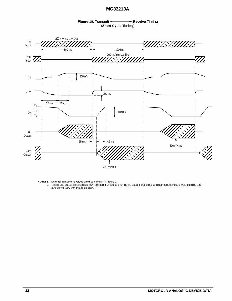
Figure 19. Transmit Receive Timing(Short Cycle Timing)
NOTE: 1. External component values are those shown in Figure 2.2. Timing and output amplitudes shown are nominal, and are for the indicated input signal and component values. Actual timing and
outputs will vary with the application.
TAIInput
TLO
RLO
CT
RAIInput
93 ms
≈ 300 ms
200 mVrms, 1.0 kHz
Rx
250 mV
TAOOutput
RAOOutput
≈ 300 ms
200 mVrms, 1.0 kHz
200 mV
18 ms 42 ms430 mVrms
430 mVrms
200 mV
Idle
Tx

MC33219A
13MOTOROLA ANALOG IC DEVICE DATA
ÎÎÎÎÎÎÎÎÎÎ
ÎÎÎÎÎÎÎÎÎÎ
ÎÎÎÎÎÎÎÎÎÎ
ÎÎÎÎÎÎÎÎÎÎ
ÎÎÎÎÎÎÎÎÎÎ
ÎÎÎÎÎÎÎÎÎÎ
ÎÎÎÎÎÎÎÎÎÎ
ÎÎÎÎÎÎÎÎÎÎ
ÎÎÎÎÎÎÎÎÎÎ
ÎÎÎÎÎÎÎÎÎÎ
ÎÎÎÎÎÎÎÎÎÎ
ÎÎÎÎÎÎÎÎÎÎ
ÎÎ
ÎÎ
ÎÎ
ÎÎ
ÎÎ
ÎÎ
ÎÎ
ÎÎ
ÎÎ
ÎÎ
ÎÎ
ÎÎ
ÎÎ
ÎÎÎÎÎÎÎÎÎÎ
ÎÎÎÎÎÎÎÎÎÎ
ÎÎÎÎÎÎÎÎÎÎ
ÎÎÎÎÎÎÎÎÎÎ
ÎÎÎÎÎÎÎÎÎÎ
ÎÎ
ÎÎ
ÎÎ
ÎÎ
ÎÎ
ÎÎÎÎÎÎÎÎÎÎ
ÎÎÎÎÎÎÎÎÎÎ
ÎÎÎÎÎÎÎÎÎÎ
ÎÎÎÎÎÎÎÎÎÎ
ÎÎÎÎÎÎÎÎÎÎ
Figure 20. Transmit Receive Timing(Long Cycle Timing)
NOTE: 1. External component values are those shown in Figure 2.2. Timing and output amplitudes shown are nominal, and are for the indicated input signal and component values. Actual timing and
outputs will vary with the application.3. Time t1 depends on the ratio of the on–off amplitude of the signal at TAI.
TAIInput
TLO
RLO
CT
RAIInput
≈ 1.0 s
200 mVrms, 1.0 kHz
TAOOutput
RAOOutput
200 mVrms, 1.0 kHz
200 mV
430 mVrms
430 mVrms
32 mVrms
250 mV
t1
ÎÎÎÎÎÎÎÎÎÎ
ÎÎÎÎÎÎÎÎÎÎ
ÎÎÎÎÎÎÎÎÎÎ
ÎÎÎÎÎÎÎÎÎÎ
ÎÎÎÎÎÎÎÎÎÎ
40 ms
72 ms
≈ 1.0 s
130 ms
200 mV
225 msTime Constant
Rx
Idle
Tx

MC33219A
14 MOTOROLA ANALOG IC DEVICE DATA
ÎÎÎÎÎÎÎÎÎÎ
ÎÎÎÎÎÎÎÎÎÎ
ÎÎÎÎÎÎÎÎÎÎ
ÎÎÎÎÎÎÎÎÎÎ
ÎÎÎÎÎÎÎÎÎÎ
ÎÎÎÎÎÎÎÎÎÎ
ÎÎÎÎÎÎÎÎÎÎ
ÎÎÎÎÎÎÎÎÎÎ
ÎÎÎÎÎÎÎÎÎÎ
ÎÎÎÎÎÎÎÎÎÎ
ÎÎÎÎÎÎÎÎÎÎ
ÎÎÎÎÎÎÎÎÎÎ
ÎÎ
ÎÎ
ÎÎ
ÎÎ
ÎÎ
ÎÎ
ÎÎ
ÎÎ
ÎÎ
ÎÎ
ÎÎ
ÎÎ
ÎÎ
ÎÎÎÎÎÎÎÎÎÎ
ÎÎÎÎÎÎÎÎÎÎ
ÎÎÎÎÎÎÎÎÎÎ
ÎÎÎÎÎÎÎÎÎÎ
ÎÎÎÎÎÎÎÎÎÎ
ÎÎ
ÎÎ
ÎÎ
ÎÎ
ÎÎ
ÎÎÎÎÎÎÎÎÎÎ
ÎÎÎÎÎÎÎÎÎÎ
ÎÎÎÎÎÎÎÎÎÎ
ÎÎÎÎÎÎÎÎÎÎ
ÎÎÎÎÎÎÎÎÎÎ
Figure 21. Transmit Receive Timing(Long Cycle Timing)
NOTE: 1. External component values are those shown in Figure 2, except the capacitor at CT is 6.8 µF.2. Timing and output amplitudes shown are nominal, and are for the indicated input signal and component values. Actual timing and
outputs will vary with the application.3. Time t1 depends on the ratio of the on–off amplitude of the signal at TAI.
TAIInput
TLO
RLO
CT
RAIInput
≈ 1.0 s
200 mVrms, 1.0 kHz
TAOOutput
RAOOutput
200 mVrms, 1.0 kHz
200 mV
430 mVrms
430 mVrms
32 mVrms
250 mV
t1
ÎÎÎÎÎÎÎÎÎÎ
ÎÎÎÎÎÎÎÎÎÎ
ÎÎÎÎÎÎÎÎÎÎ
ÎÎÎÎÎÎÎÎÎÎ
ÎÎÎÎÎÎÎÎÎÎ
20 ms
32 ms
≈ 1.0 s
90 ms
200 mV
100 msTime Constant
Rx
Idle
Tx

MC33219A
15MOTOROLA ANALOG IC DEVICE DATA
Figure 22. Chip Disable Timing
NOTE: Enable time t1 depends on the length of tOFF according to the following chart:
CD Input(Pin 8)
tOFF
5.0 µsÎÎÎÎÎÎÎÎÎÎÎÎÎÎ
ÎÎÎÎÎÎÎÎÎÎÎÎÎÎ
ÎÎÎÎÎÎÎÎÎÎÎÎÎÎ
ÎÎÎÎÎÎÎÎÎÎÎÎÎÎ
ÎÎÎÎ
ÎÎÎÎ
ÎÎÎÎ
ÎÎÎÎ
ÎÎÎÎÎÎÎÎÎÎÎÎÎÎ
ÎÎÎÎÎÎÎÎÎÎÎÎÎÎ
ÎÎÎÎÎÎÎÎÎÎÎÎÎÎ
ÎÎÎÎÎÎÎÎÎÎÎÎÎÎ
ÎÎÎÎ
ÎÎÎÎ
ÎÎÎÎ
ÎÎÎÎ
Figure 23. Mute Timing
Output atRAO, TAO
Mute Input(Pin 18)
Output atMCO
t1
1.5 µs 5.0 µs
≤ 50 ms100 ms500 ms5.0 s
tOFF–
5.0 µs64 ms80 ms
to 60%
5.0 µs14 ms72 ms100 ms
to 100%
t1

MC33219A
16 MOTOROLA ANALOG IC DEVICE DATA
FUNCTIONAL DESCRIPTION
IntroductionThe fundamental difference between the operation of a
speakerphone and a telephone handset is that ofhalf–duplex versus full–duplex. The handset is full duplex,meaning conversation can occur in both directions (transmitand receive) simultaneously. This is possible due to boththe low sound level at the receiver, and the fact that theacoustic coupling from the earpiece to the mouthpiece isalmost non–existent (the receiver is normally held against aperson’s ear). The loop gain from the receiver to themicrophone and through the circuit is well below thatneeded to sustain oscillations.
A speakerphone, on the other hand, has higher gain levelsin both the transmit and receive paths, and attempting toconverse full duplex results in oscillatory problems due to theloop that exists within the speakerphone circuit. The loop isformed by the hybrid, the acoustic coupling (speaker tomicrophone), and the transmit and receive paths (betweenthe hybrid and the speaker/microphone). The only practicaland economical method used to date is to design thespeakerphone to function in a half duplex mode; i.e., only oneperson speaks at a time, while the other listens. To achievethis requires a circuit which can detect who is talking (inreality, who is talking louder), switch on the appropriate path(transmit or receive), and switch off (attenuate) the otherpath. In this way, the loop gain is maintained less than unity.When the talkers exchange function, the circuit must quicklydetect this, and switch the circuit appropriately. By providingspeech level detectors, the circuit operates in a “hands–free”mode, eliminating the need for a “push–to–talk” switch.
The MC33219A provides the necessary circuitry toperform a voice switched, half duplex, speakerphonefunction. The IC includes transmit and receive attenuators,pre–amplifiers, level detectors and background noisemonitors for each path. An attenuator control circuitautomatically adjusts the gain of the transmit and receiveattenuators based on the relative strengths of the voicesignals present, the volume control, and the supply voltage(when low). The detection sensitivity and timing areexternally controllable. Please refer to the Block Diagram(Figure 2) when reading the following sections.
Transmit and Receive AttenuatorsThe transmit and receive attenuators are complementary,
performing a log–antilog function. When one is at maximumgain (≈ 6.7 dB), the other is at maximum attenuation(≈ –46 dB); they are never both fully on or fully off. Bothattenuators are controlled by a single output from theAttenuator Control Circuit which ensures the sum of their
gains will remain constant at a typical value of –40 dB.Their purpose is to provide the half–duplex operationrequired in a speakerphone.
The attenuators are non–inverting, and have a usablebandwidth of 50 kHz. The input impedance of eachattenuator (TXI and RXI) is nominally 100 kΩ (see Figure 24),and the input signal should be limited to 300 mVrms (850 mVp–p) to prevent distortion. That maximum recommendedinput signal is independent of the volume control setting. Boththe input and output are biased at ≈ VB. The outputimpedance is <10 Ω until the output current limit (see specs)is reached.
Figure 24. Attenuator Input Stage
VB
TAI(RAI)
VB
90 k10 k
The attenuators are controlled by the single output of theAttenuator Control Circuit, which is measurable at CT (Pin 7).When the circuit detects speech signals directing it to thereceive mode (by means of the level detectors describedbelow), an internal current source of 90 µA will charge the CTcapacitor to a voltage positive with respect to VB (seeFigure 25). At the maximum volume control setting, thisvoltage will be approximately 150 mV, and the receiveattenuator will have a gain of 6.7 dB. When the circuit detectsspeech signals directing it to the transmit mode, an internalcurrent source of 50 µA will take the capacitor toapproximately –100 mV with respect to VB (the transmitattenuator will have a gain of 6.7 dB). When there is nospeech present in either path, the current sources are shutoff, and the voltage at CT will decay to be equal to VB. This isthe idle mode, and the attenuators’ gains are nearly halfwaybetween their fully ON and fully OFF positions (–25 dB for theRx attenuator, –16 dB for the Tx attenuator). Monitoring theCT voltage (with respect to VB) is the most direct method ofmonitoring the circuit’s mode, and its response.
The inputs to the Attenuator Control Section are six: TheTx–Rx comparator operated by the level detectors, twobackground noise monitors, the volume control, the dialtonedetector, and the AGC circuit. These six functions aredescribed as follows.

MC33219A
17MOTOROLA ANALOG IC DEVICE DATA
Figure 25. C T Attenuator Control Circuit
VB
I190 µA
ToAttenuators
RT
CT
Tx
TX–Rx Comp.Vol. ControlDial Tone Det.
Voltage Clamps
Control CircuitI250 µA
CT
MC33219A
Rx
BackgroundMonitors
AGC
Level DetectorsThere are two identical level detectors: one on the receive
side and one on the transmit side (refer to Figure 26). Eachlevel detector is a high gain amplifier with back–to–backdiodes in the feedback path, resulting in non–linear gain,which permits operation over a wide dynamic range ofspeech levels. Refer to the graphs of Figures 6, 7 and 8 fortheir DC and AC transfer characteristics. The sensitivity ofeach level detector is determined by the external resistor andcapacitor at their input (TLI and RLI). The output charges anexternal capacitor through a diode and limiting resistor, thusproviding a DC representation of the input AC signal level.The outputs have a quick rise time (determined by thecapacitor and an internal 500 Ω resistor), and a slow decaytime set by an internal current source and the capacitor. Thecapacitors on the two outputs should have the same value(±10%) to prevent timing problems.
Referring to Figure 2, the outputs of the two level detectorsdrive the Tx–Rx comparator. The comparator’s output statedepends on whether the transmit or receive speech signal isstronger, as sensed by the level detectors. The AttenuatorControl Circuit uses this signal, along with the backgroundnoise monitors, to determine which mode to set.
Figure 26. Level Detector
TLO(RLO)1.0 µF
500 Ω
2.0 µA
TLI(RLI)
VB
RCSignalInput
External Component Values are Application Dependent.
Background Noise MonitorsThe purpose of the background noise monitors is to
distinguish speech (which consists of bursts) frombackground noise (a relatively constant signal). There aretwo background noise monitors: one for the receive path andone for the transmit path. Refering to Figure 27, each isoperated on by a level detector, which provides a DCvoltage representative of the combined speech and noiselevel. However, the peaks, valleys, and bursts, which arecharacteristic of speech, will cause the DC voltage (at CP2or RLO) to increase relatively quickly, causing the output ofthe next amplifier to also rise quickly. If that increaseexceeds the 36 mV offset, and at a speed faster than thetime constant at CPT (CPR), the output of the lastcomparator will change, indicating the presence of speechto the attenuator control circuit. This will keep the circuit ineither the transmit or the receive mode, depending on whichside has the stronger signals. When a new continuous signalis applied, the time constant at CPT (CPR) determines howlong it takes the circuit to decide that the new sound iscontinuous, and is therefore background noise. The systemrequires that the average speech signal be stronger than thebackground noise level (by 6.0–7.0 dB) for proper speechdetection.
When only background noise is present in both paths, theoutput of the monitors will indicate the absence of speech,allowing the circuit to go to the idle mode.
AGC CircuitIn the receive mode only, the AGC circuit decreases the
gain of the receive attenuator when the supply voltage atVCC falls below 3.5 V, according to the graph of Figure 5.The gain of the transmit path changes in a complementarymanner.
The purpose of this feature is to reduce the power (andcurrent) used by the speaker when the speakerphone ispowered by the phone line, and is connected to a longtelephone line, where the available power is limited.Reducing the speaker power controls the voltage sag at VCC,reduces clipping and distortion at the speaker output, andprevents possible erratic operation.

MC33219A
18 MOTOROLA ANALOG IC DEVICE DATA
Figure 27. Background Noise Monitor
18.6 k
500 Ω
XDI(RLI)
VB
RCSignalInput
31.7 k
VB
CP2(RLO)
CPT(CPR)
2.0 µA36 mV
47 µF
100 k
To AttenuatorControl Circuit
BackgroundNoise Monitor VCC
1.0 µFExternal Component Values are Application Dependent.
Volume ControlThe volume control input at VLC (Pin 19) is sensed as a
voltage with respect to VB. The volume control affects theattenuators in the receive mode only . It has no effect in theidle or transmit modes.
By varying the voltage at the VLC pin (Pin 19), the volumecontrol varies the gain of the attenuators. Maximum receiveattenuator gain (6.7 dB) occurs when VLC = VB. As VLC isreduced below VB, the gain of the receive attenuator isreduced, and the transmit attenuator gain increases in acomplementary manner. The usable range of the VLC pin is≈ 1.1 V for VCC ≥ 3.5 V, providing a range of ≈ 40 dB (seeFigure 4). At VCC < 3.5 V, the range is reduced due to thelower VB voltage, and the AGC function.
The configuration of the external volume controlpotentiometer circuit depends on whether the VCC supplyvoltage is regulated or if it varies, such as in a phone linepowered circuit (see Figure 28). If the supply voltage isregulated, the circuit on the left can be used. The value of thelower resistor (R1) depends on the value of VCC, so thatPin 19 can be varied from VB to ≈ 1.1 V below VB.
In a phone line powered circuit, the value of VCC, andconsequently VB, will vary with line length and with theamount of sound at the speaker. In this case, the circuit onthe right side of Figure 28 must be used to provide a fixedreference voltage for the potentiometer. With this circuit, thevolume setting will not vary when VCC is ≥ 3.5 V. As VCC fallsbelow 3.5 V, the zener diode will drop out of regulation, butthe AGC circuit will ensure that instabilities do not occur.
The bias current at VLC flows out of the pin and dependson the voltage at the pin (see Figure 16). The capacitor fromVLC to VB helps reduce any effects of ripple or noise on VB.
Figure 28. Volume Control
50 k50 k
R1
3160
To VLC(Pin 19)
0.1
VB
VolumeControl
To VLC(Pin 19)
0.1
VolumeControl
VB
6.5 V6.0 V5.0 V4.0 V
VCC86 k72 k50 k25 k
R1
Regulated Supply Unregulated Supply
LM38
5-1.
2
Dial Tone DetectorWhen the speakerphone is initially taken off–hook, the dial
tone signal will switch the circuit to the receive mode.However, since the dial tone is a continuous signal, theMC33219A would consider it as background noise ratherthan speech, and would therefore switch from receive to idle,causing the dial tone sound level to fade. The dial tonedetector prevents the fading by disabling the backgroundnoise monitor.
The dial tone detector is a comparator with one sideconnected to the receive attenuator input (RAI), and the otherinput connected to VB with a –20 mV offset (see Figure 29).If the circuit is in the receive mode and the incoming signalhas peaks greater than 20 mV (14 mV rms), the comparator’soutput will change, disabling the receive idle mode. Thereceive attenuator will then be at a setting determined solelyby the volume control. NOTE: The dial tone detector is not afrequency discriminating circuit.
Figure 29. Dial Tone Detector
To AttenuatorControl Circuit
To Rx Attenuator
VB
20 mV
RAI
Microphone Amplifier, MuteThe microphone amplifier (Pins 20, 21) has the
non–inverting input internally connected to VB, while theinverting input and the output are pinned out. Unlike most opamps, the amplifier has an all NPN output stage, whichmaximizes phase margin and gain–bandwidth. This featureensures stability at gains less than unity, as well as with awide range of reactive loads. The open loop gain is typically70 dB (f < 100 Hz), and the gain–bandwidth is typically1.5 MHz. The maximum p–p output swing, for 1.0% or lessdistortion, is shown in Figure 14. The output impedance is<10 Ω until current limiting is reached (typically 2.0 mA peak).The input bias current at MCI is typically 30 nA out of the pin.
The mute function (Pin 18), when activated, will reduce thegain of the amplifier by shorting the external feedbackresistor (RMF in Figure 30). The amplifier is not disabled inthis mode; MCO remains a low impedance output, and MCIremains a virtual ground at VB. The amount of muting (the
MC33219A
19MOTOROLA ANALOG IC DEVICE DATA
change in gain) depends on the value of the externalfeedback resistor, according to the graph of Figure 15.Muting occurs as the mute input pin is taken from ≈ 1.0 V to≈ 1.4 V. The voltage on this pin must be ≤ 0.8 V for normaloperation, and ≥ 2.0 V for muting. See Figure 10 for inputcurrent requirements. The input must be kept within therange of VCC and GND. If the input is taken more than 0.4 Vabove VCC or below GND excessive currents will flow, andthe device’s operation will be distorted. If the mute function isnot used, the pin should be grounded.
Figure 30. Microphone Amplifier and Mute
VCC
VBRMIFrom Microphone
50 k
50 k
Mute
RMF
MCOMCI
Receive AmplifierThe receive amplifier (Pins 16, 17) has the non–inverting
input internally connected to VB, while the inverting input andthe output are pinned out. Unlike most op amps, the amplifierhas an all NPN output stage, which maximizes phase marginand gain–bandwidth. This feature ensures stability at gainsless than unity, as well as with a wide range of reactive loads.The open loop gain is typically 70 dB (f < 100 Hz), and thegain–bandwidth is typically 1.5 MHz. The maximum p–poutput swing for 1.0% or less distortion is shown in Figure 14.The output impedance is <10 Ω until current limiting isreached (typically 2.0 mA peak). The input bias current atRXI is typically 30 nA out of the pin.
Power Supply, V B and Chip DisableThe power supply voltage at Pin 24 is to be between 3.5
and 6.5 V for normal operation, and down to 2.7 V with theAGC in effect (see AGC section). The supply current requiredis typically 3.2 mA in the idle mode, and ≈ 4.0 mA in thetransmit and receive modes. Figure 11 shows the supplycurrent for both the normal and disabled modes.
The output voltage at VB (Pin 6) is approximately equal to(VCC – 0.7)/2, and provides an AC ground for the internalamplifiers and the system. The output impedance at VB isapproximately 600 Ω, and in conjunction with the externalcapacitor at VB forms a low pass filter for power supply noiserejection. The choice of the VB capacitor size is applicationdependent based on whether the circuit is powered by thetelephone line or a regulated supply. See Figure 13 forPSRR information. Since VB biases the microphone andreceive amplifiers, the amount of supply rejection at theiroutputs is a function of the rejection at VB, as well as thegains of the amplifiers.
The amount of current which can be sourced out of the VBpin depends on the VCC voltage (see Figure 12). Drawingcurrent in excess of that shown in Figure 12 will cause VB todrop low enough to disrupt the circuit’s operation. This pincan sink ≈ 100 µA when enabled, and 0 µA when disabled.
The Chip Disable (Pin 8) permits powering down the ICfor power conservation. With CD between 0 and 0.8 V,normal operation is in effect. With CD between 2.0 V andVCC, the IC is powered down, and the supply current dropsto about 110 µA (at VCC = 5.0 V, see Figure 11). When CD ishigh, the microphone and receive amplifiers, the leveldetectors, and the two attenuators are disabled (theiroutputs go to a high impedance). The background noisemonitors are disabled, and Pins 3 and 10 will go to VCC. TheVB output, however, remains active, except that it cannotsink any current.
The CD input must be kept within the range of VCC andGND. See Figure 9 for input current requirements. If the inputis taken more than 0.4 V above VCC or below GND excessivecurrents will flow, and the device’s operation will be distorted.If the disable function is not used, the pin should beconnected to ground.

MC33219A
20 MOTOROLA ANALOG IC DEVICE DATA
APPLICATIONS INFORMATION
Switching and Response Time TheoryThe switching time of the MC33219A circuit is dominated
first by the components at CT (Pin 7, see Figure 2), andsecond by the capacitors at the level detector outputs (RLO,TLO).
The transition time to receive or to transmit mode fromeither idle or the other mode is determined by the capacitorat CT, along with the internal current sources (refer toFigure 25). The switching time is:
TV CT
IWhen switching from idle to receive, ∆V = 150 mV,
I = 90 µA, the CT capacitor is 15 µF, and ∆T calculates to≈ 25 ms. When switching from idle to transmit, ∆V = 100 mV,I = 50 µA, the CT capacitor is 15 µF, and ∆T calculates to≈ 30 ms.
When the circuit switches to idle, the internal currentsources are shut off, and the time constant is determined bythe CT capacitor and RT, the external resistor (seeFigure 25). With CT = 15 µF, and RT = 15 kΩ, the timeconstant is ≈ 225 ms, giving a total switching time of ≈ 0.68 s(for 95% change). The switching period to idle begins whenboth speakers have stopped talking. The switching time backto the original mode will depend on how soon that speakerbegins speaking again. The sooner the speaking startsduring the “decay to idle” period, the quicker the switchingtime, since a smaller voltage excursion is required. Thatswitching time is determined by the internal current sourcesas described above.
When the circuit switches directly from receive totransmit (or vice versa), the total switching time dependsnot only on the components and currents at the CT pin, butalso on the response of the level detectors, the relativeamplitude of the two speech signals, and the mode of thecircuit, since the two level detectors are connecteddifferently to the two attenuators.
The rise time of the level detector’s outputs (RLO, TLO) isnot significant since it is so short. The decay time, however,provides a significant part of the “hold time” necessary tohold the circuit (in transmit or receive) during the normalpauses in speech. The capacitors at the two outputs mustbe equal value (±10%) to prevent problems in timing andlevel response.
The components at the inputs of the level detectors (RLI,TLI) do not affect the switching time, but rather affect therelative signal levels required to switch the circuit, as well asthe frequency response of the detectors. They must beadjusted for proper switching response as described later inthis section.
Switching and Response Time MeasurementsUsing burst of 1.0 kHz sine waves to force the circuit to
switch among its modes, the timing results were measuredand are indicated in Figures 17–21.
a) In Figure 17, when a signal is applied to the transmitattenuator only (normally via the microphone and themicrophone amplifier), the transmit background noisemonitor immediately indicates the “presence of speech” asevidenced by the fact that CPT begins rising. The slope ofthe rising CPT signal is determined by the external resistorand capacitor on that pin. Even though the transmit
attenuator is initially in the idle mode (–16 dB), there issufficient signal at its output to cause TLO to increase. Theattenuator control circuit then forces the circuit to thetransmit mode, evidenced by the change at the CT pin. Theattenuator output signal is then 6.7 dB above the input.
With the steady sine wave applied to the transmit input,the circuit will stay in the transmit mode until the CPT pin getsto within 36 mV of its final value. At that point, the internalcomparator (see Figure 27) switches, indicating to theattenuator control circuit that the signal is not speech, butrather it is a steady background noise. The circuit now beginsto decay to idle, as evidenced by the change at CT and TLO,and the change in amplitude at TAO.
When the input signal at TAI is removed (or reduced), theCPT pin drops quickly, allowing the circuit to quickly respondto any new speech which may appear afterwards. Thevoltage at CT decays according to the time constant of itsexternal components, if not already at idle.
The voltage change at CP2, CPT, and TAO depends onthe input signal’s amplitude and the components at XDI andTLI. The change at CT is internally fixed at the level shown.The timing numbers shown depend both on the signalamplitudes and the components at the CT and CPT pins.
b) Figure 18 indicates what happens when the same signalis applied to the receive side only. RLO and CPR reactsimilarly to TLO and CPT. However, the circuit does not switchto idle when CPR finishes transitioning since the dial tonedetector disables the background noise monitor, allowing thecircuit to stay in the receive mode as long as there is a signalpresent. If the input signal amplitude had been less than thedial tone detector’s threshold, the circuit response would havebeen similar to that shown in Figure 17. The voltage changeat CT depends on the setting of the volume control (Pin 19).The 150 mV represent maximum volume setting.
c) Figure 19 indicates the circuit response when transmitand receive signals are alternately applied, with relatively shortcycle times (300 ms each) so that neither attenuator will beginto go to idle during its “on” time. Figure 20 indicates the circuitresponse with longer cycle times (1.0 s each), where thetransmit side is allowed to go to idle. Figure 21 is the same asFigure 20, except the capacitor at CT has been reduced from15 µF to 6.8 µF, providing a quicker switching time. Thereactions at the various pins are shown. The response times atTAO and RAO are different, and typically slightly longer thanwhat is shown in Figures 17 and 18 due to:
– the larger transition required at the CT pin,– the greater difference in the levels at RLO and TLO due
to the positions of the attenuators as well as their decaytime, and
– response time of the background noise monitors.The timing responses shown in these three figures are
representative for those input signal amplitudes and burstdurations. Actual response time will vary for different signalconditions.
NOTE: While it may seem desirable to decrease theswitching time between modes by reducing the capacitor atCT, this should be done with caution for two reasons:
1) If the switching time is too short, the circuit responsemay appear to be “too quick” to the user, who may considerits operation erratic. The recommended values in this datasheet, along with the accompanying timings, provide what

MC33219A
21MOTOROLA ANALOG IC DEVICE DATA
experience has shown to be a “comfortable response” bythe circuit.
2) The distortion in the receive attenuator will increase asthe CT capacitor value is decreased. The extra THD will bemost noticeable at the lower frequencies and at the lowerampitudes. Table 1 provides a guideline for this issue.
Table 1. THD versus C T CapacitorÁÁÁÁÁ
ÁÁÁÁÁ
ÁÁÁÁÁ
ÁÁÁÁÁ
CTCapacitor
ÁÁÁÁ
ÁÁÁÁ
ÁÁÁÁ
ÁÁÁÁ
Idle – RxTransition
ÁÁÁÁÁ
ÁÁÁÁÁ
ÁÁÁÁÁ
ÁÁÁÁÁ
Input@ RAI
ÁÁÁ
ÁÁÁ
ÁÁÁ
ÁÁÁ
Freq.
ÁÁÁÁ
ÁÁÁÁ
ÁÁÁÁ
ÁÁÁÁ
THD@ RAO
ÁÁÁÁÁ
ÁÁÁÁÁ
ÁÁÁÁÁ
ÁÁÁÁÁ
15 µF
ÁÁÁÁ
ÁÁÁÁ
ÁÁÁÁ
ÁÁÁÁ
25 ms
ÁÁÁÁÁ
ÁÁÁÁÁ
ÁÁÁÁÁ
ÁÁÁÁÁ
20 mVrms
ÁÁÁ
ÁÁÁ
ÁÁÁ
ÁÁÁ
300 Hz
ÁÁÁÁ
ÁÁÁÁ
ÁÁÁÁ
ÁÁÁÁ
1.2%
ÁÁÁÁÁ
ÁÁÁÁÁ
ÁÁÁÁÁ
ÁÁÁÁÁ
ÁÁÁÁ
ÁÁÁÁ
ÁÁÁÁ
ÁÁÁÁ
ÁÁÁÁÁ
ÁÁÁÁÁ
ÁÁÁÁÁ
ÁÁÁÁÁ
ÁÁÁ
ÁÁÁ
ÁÁÁ
ÁÁÁ
1.0 KHz
ÁÁÁÁ
ÁÁÁÁ
ÁÁÁÁ
ÁÁÁÁ
0.25%
ÁÁÁÁÁ
ÁÁÁÁÁ
ÁÁÁÁÁ
ÁÁÁÁÁ
ÁÁÁÁ
ÁÁÁÁ
ÁÁÁÁ
ÁÁÁÁ
ÁÁÁÁÁ
ÁÁÁÁÁ
ÁÁÁÁÁ
ÁÁÁÁÁ
100 mVrms
ÁÁÁ
ÁÁÁ
ÁÁÁ
ÁÁÁ
300 Hz
ÁÁÁÁ
ÁÁÁÁ
ÁÁÁÁ
ÁÁÁÁ
0.5%
ÁÁÁÁÁ
ÁÁÁÁÁ
ÁÁÁÁÁ
ÁÁÁÁÁ
ÁÁÁÁ
ÁÁÁÁ
ÁÁÁÁ
ÁÁÁÁ
ÁÁÁÁÁ
ÁÁÁÁÁ
ÁÁÁÁÁ
ÁÁÁÁÁ
ÁÁÁ
ÁÁÁ
ÁÁÁ
ÁÁÁ
1.0 KHz
ÁÁÁÁ
ÁÁÁÁ
ÁÁÁÁ
ÁÁÁÁ
0.2%
ÁÁÁÁÁ
ÁÁÁÁÁ
ÁÁÁÁÁ
ÁÁÁÁÁ
6.8 µF
ÁÁÁÁ
ÁÁÁÁ
ÁÁÁÁ
ÁÁÁÁ
12 ms
ÁÁÁÁÁ
ÁÁÁÁÁ
ÁÁÁÁÁ
ÁÁÁÁÁ
20 mVrms
ÁÁÁ
ÁÁÁ
ÁÁÁ
ÁÁÁ
300 Hz
ÁÁÁÁ
ÁÁÁÁ
ÁÁÁÁ
ÁÁÁÁ
5.0%
ÁÁÁÁÁ
ÁÁÁÁÁ
ÁÁÁÁÁ
ÁÁÁÁÁ
ÁÁÁÁ
ÁÁÁÁ
ÁÁÁÁ
ÁÁÁÁ
ÁÁÁÁÁ
ÁÁÁÁÁ
ÁÁÁÁÁ
ÁÁÁÁÁ
ÁÁÁ
ÁÁÁ
ÁÁÁ
ÁÁÁ
1.0 KHz
ÁÁÁÁ
ÁÁÁÁ
ÁÁÁÁ
ÁÁÁÁ
0.7%
ÁÁÁÁÁ
ÁÁÁÁÁ
ÁÁÁÁÁ
ÁÁÁÁÁ
ÁÁÁÁ
ÁÁÁÁ
ÁÁÁÁ
ÁÁÁÁ
ÁÁÁÁÁ
ÁÁÁÁÁ
ÁÁÁÁÁ
ÁÁÁÁÁ
100 mVrms
ÁÁÁ
ÁÁÁ
ÁÁÁ
ÁÁÁ
300 Hz
ÁÁÁÁ
ÁÁÁÁ
ÁÁÁÁ
ÁÁÁÁ
1.3%
ÁÁÁÁÁ
ÁÁÁÁÁ
ÁÁÁÁÁ
ÁÁÁÁÁ
ÁÁÁÁ
ÁÁÁÁ
ÁÁÁÁ
ÁÁÁÁ
ÁÁÁÁÁ
ÁÁÁÁÁ
ÁÁÁÁÁ
ÁÁÁÁÁ
ÁÁÁ
ÁÁÁ
ÁÁÁ
ÁÁÁ
1.0 KHz
ÁÁÁÁ
ÁÁÁÁ
ÁÁÁÁ
ÁÁÁÁ
0.35%
ÁÁÁÁÁ
ÁÁÁÁÁ
ÁÁÁÁÁ
ÁÁÁÁÁ
3.0 µF
ÁÁÁÁ
ÁÁÁÁ
ÁÁÁÁ
ÁÁÁÁ
5.0 ms
ÁÁÁÁÁ
ÁÁÁÁÁ
ÁÁÁÁÁ
ÁÁÁÁÁ
20 mVrms
ÁÁÁ
ÁÁÁ
ÁÁÁ
ÁÁÁ
300 Hz
ÁÁÁÁ
ÁÁÁÁ
ÁÁÁÁ
ÁÁÁÁ
11%
ÁÁÁÁÁ
ÁÁÁÁÁ
ÁÁÁÁÁ
ÁÁÁÁÁ
ÁÁÁÁ
ÁÁÁÁ
ÁÁÁÁ
ÁÁÁÁ
ÁÁÁÁÁ
ÁÁÁÁÁ
ÁÁÁÁÁ
ÁÁÁÁÁ
ÁÁÁ
ÁÁÁ
ÁÁÁ
ÁÁÁ
1.0 KHz
ÁÁÁÁ
ÁÁÁÁ
ÁÁÁÁ
ÁÁÁÁ
1.8%
ÁÁÁÁÁ
ÁÁÁÁÁ
ÁÁÁÁÁ
ÁÁÁÁÁ
ÁÁÁÁ
ÁÁÁÁ
ÁÁÁÁ
ÁÁÁÁ
ÁÁÁÁÁ
ÁÁÁÁÁ
ÁÁÁÁÁ
ÁÁÁÁÁ
100 mVrms
ÁÁÁ
ÁÁÁ
ÁÁÁ
ÁÁÁ
300 Hz
ÁÁÁÁ
ÁÁÁÁ
ÁÁÁÁ
ÁÁÁÁ
2.6%
ÁÁÁÁÁ
ÁÁÁÁÁ
ÁÁÁÁÁ
ÁÁÁÁÁ
ÁÁÁÁ
ÁÁÁÁ
ÁÁÁÁ
ÁÁÁÁ
ÁÁÁÁÁ
ÁÁÁÁÁ
ÁÁÁÁÁ
ÁÁÁÁÁ
ÁÁÁ
ÁÁÁ
ÁÁÁ
ÁÁÁ
1.0 KHz
ÁÁÁÁ
ÁÁÁÁ
ÁÁÁÁ
ÁÁÁÁ
0.7 %
Considerations in the Design of a SpeakerphoneThe design and adjustment of a speakerphone involves
human interface issues as well as proper signal levels.Because of this fact, it is not practical to do all of the designmathematically. Certain parts of the design must be done bytrial and error, most notably the switching response and the“How does it sound?” part of the testing. Among therecommendations for a successful design are:
1) Design the enclosure concurrently with theelectronics. Do not leave the case design to the end as its
properties are just as important (just as equally important) asthe electronics. One of the major issues involved in aspeakerphone design is the acoustic coupling of the speakerto the microphone, which must be minimized. Thisparameter is dependent entirely on the design of theenclosure, the mounting of the speaker and the microphone,and their characteristics.
2) Ensure the speaker is optimally mounted. This factalone can make a difference of several dB in the sound levelfrom the speaker, as well as the sound quality. The speakermanufacturer should be consulted for this information.
3) Do not breadboard the circuit with the microphone andspeaker hanging out in midair. It will not work. The speakerand microphone must be in a suitable enclosure, preferablyone resembling the end product. If this is not feasible,temporarily use some other properly designed enclosure,such as one of the many speakerphones on the market.
4) Do not breadboard the circuit on a wirewrapped boardor a plug–in prototyping board. Use a PC board, preferablywith a ground plane. Proper filtering of the supply voltage atthe VCC pin is essential.
5) The speakerphone must be tested with the intendedhybrid and connected to a phone line or phone line simulator.The performance of the hybrid is just as important as theenclosure and the speakerphone IC.
6) When testing the speakerphone, be conscious of theenvironment. If the speakerphone is in a room with largewindows and tile floors, it will sound different than if it is in acarpeted room with drapes. Additionally, be conscious of thebackground noise in a room.
7) When testing the speakerphone on a phone line, makesure the person at the other end of the phone line is not in thesame room as the speakerphone.
Design ProcedureA recommended sequence follows in Figure 31,
assuming the end product enclosure is available, with theintended production microphone and speaker installed, andthe PC boards or temporary substitutes installed.
Figure 31. Basic Block Diagram for Design Purposes
AcousticCoupling Control HybridGST
(GAC)
V1
Tip
Ring
R1
V2
R2Rx Attenuator
VM
MCI
MikeAmp
SpeakerAmp
RAO
MCO
RAI
TAOTAI
I1
I2
RXO RXI
TLI
RLI
Tx Attenuator
Speaker
Microphone

MC33219A
22 MOTOROLA ANALOG IC DEVICE DATA
1) Design the hybrid, ensuring proper interface with thephone line for both DC and AC characteristics. The returnloss must be adjusted to comply with the appropriateregulatory agency. The sidetone should then be adjustedaccording to the intent of the product. If the product is aspeakerphone only (without a handset), the sidetone gain(GST) should be adjusted for maximum loss. If a handset ispart of the end product, the sidetone must be adjusted for theminimum acceptable sidetone levels in the handset.Generally, for the speakerphone interface, 10–20 dBsidetone loss is preferred for GST.
2) Check the acoustic coupling of the enclosure (GAC inFigure 31). With a steady sound coming out of the speaker,measure the rms voltage on the speaker terminals and the rmsvoltage out of the microphone. Experience has shown that theloss should be at least 40 dB, preferably 50 dB. This shouldbe checked over the frequency range of 20 Hz to 10 kHz.
3) Adjust the transmit path for proper signal levels, basedon the lowest speech levels as well as the loudest. Based onthe typical levels from commonly available microphones, again of about 35–45 dB is required from the microphoneterminals to Tip and Ring. Most of that gain should be in themicrophone amplifier to make best use of the transmitattenuator, but the maximum input level at TAI must not beexceeded. If a signal generator is used instead of amicrophone for testing, the circuit can be locked into thetransmit mode by grounding CPT (Pin 3). Frequencyresponse can generally be tailored with capacitors at themicrophone amplifier.
4) Adjust the receive path for proper signal levels based onthe lowest speech levels as well as the loudest. A gain ofabout 30 dB is required from Tip and Ring to the speakerterminals for most applications (at maximum volume). Mostof that gain should be in the receive amplifier (at RXI, RXO) tomake best use of the receive attenuator, but the maximuminput level at RAI must not be exceeded. If a signal generatoris used for signal injection during testing, the circuit can belocked into the receive mode by grounding CPR (Pin 10),although this is usually not necessary since the dial tonedetector will keep the circuit in the receive mode. Frequencyresponse can generally be tailored with capacitors at thereceive amplifier.
5) Check that the loop gain (i.e., the receive path gain +acoustic coupling gain + transmit path gain + sidetone gain)is less than 0 dB over all frequencies. If not, “singing” willoccur: a steady oscillation at some audible frequency.
6) a) The final step is to adjust the resistors at the leveldetector inputs (RLI and TLI) for proper switching response(the switchpoint occurs when I1 = I2). This has to be the laststep, as the resistor values depend on all of the aboveadjustments, which are based on the mechanical, as well asthe electrical, characteristics of the system. NOTE: Anextreme case of level detector misadjustment can result in“motorboating”. In this condition, with a receive signalapplied, sound from the speaker enters the microphone, andcauses the circuit to switch to the transmit mode. This causesthe speaker sound to stop (as well as the sound into themicrophone), allowing the circuit to switch back to the receivemode. This sequence is then repeated, usually, at a rate of afew Hz. The first thing to check is the acoustic coupling, andthen the level detectors.
b) Starting with the recommended values for R1 and R2 (inFigure 2), hold a normal conversation with someone onanother phone. If the resistor values are not optimum, one ofthe talkers will dominate, and the other will have difficulty
getting through. If, for example, the person at thespeakerphone is dominant, the transmit path is overlysensitive, and the receive path is not sensitive enough. In thiscase, R1 (at TLI) should be increased, or R2 (at RLI)decreased, or both. Their exact value is not critical at thispoint, only their relative value. Keeping R1 and R2 in therange of 2.0–20 k, adjust them until a suitable switchingresponse is found.
c) Then have the person at the other end of the phone linespeak loud continuously, or connect to a recording which issomewhat strong. Monitor the state of the circuit (bymeasuring the CT versus VB pins, and by listening carefully tothe speaker) to check that the sound out of the speaker is notattempting to switch the circuit to the transmit side (throughacoustic coupling). If it is, increase R1 (at TLI) in small stepsjust enough to stop the switching (this desensitizes thetransmit side). If R1 has been changed a large amount, it maybe necessary to readjust R2 for switching response. If thiscannot be achieved in a reasonable manner, the acousticcoupling is too strong.
d) Next, have the person at the speakerphone speaksomewhat loudly, and again monitor the state of the circuit,primarily by having the person at the other end listen carefullyfor fading. If there is obvious fading of the sound, increase R2so as to desensitize the receive side. Increase R2 justenough to stop the fading. If this cannot be achieved in areasonable manner, the sidetone coupling is too strong.
e) If necessary, readjust R1 and R2 a small amountrelative to each other, to further optimize the switchingresponse.
Transmit/Receive Detection PriorityAlthough the MC33219A was designed to have an idle
mode such that the transmit side has a small priority (the idlemode position is closer to the full transmit side), the idle modeposition can be moved with respect to the transmit or thereceive side. With this done, the ability to gain control of thecircuit by each talker will be changed.
By connecting a resistor from CT (Pin 7) to ground, thecircuit will be biased more towards the transmit side. Theresistor value is calculated from:
R RT VBV
1where R is the added resistor, RT is the resistor normallybetween Pins 6 and 7 (typically 15 kΩ), and ∆V is the desiredchange in the CT voltage at idle.
By connecting a resistor from CT (Pin 7) to VCC, the circuitwill be biased towards the receive side. The resistor value iscalculated from:
R RT VCC –VB
V 1
R, RT, and ∆V are the same as above. Switching responseand the switching time will be somewhat affected in eachcase due to the different voltage excursions required to get totransmit and receive from idle. For practical considerations,the ∆V shift should not exceed 50 mV.
Disabling the Idle ModeFor testing or circuit analysis purposes, the transmit or
receive attenuators can be set to the ON position, even withsteady signals applied, by disabling the background noisemonitors. Grounding the CPR pin will disable the receivebackground noise monitor, thereby indicating the “presence

MC33219A
23MOTOROLA ANALOG IC DEVICE DATA
of speech” to the attenuator control block. Grounding CPTdoes the same for the transmit path.
Additionally, the receive background noise monitor isautomatically disabled by the dial tone detector whenever thereceive signal exceeds the detector’s threshold.
Dial Tone Detector ThresholdThe threshold for the dial tone detector is internally set at
≈ 20 mV (14 mVrms) below VB (see Figure 29). Thatthreshold can be adjusted if desired by changing the bias atRAI. The method used depends on how the input of thereceive attenuator is connected to other circuitry.
a) If the attenuator input (RAI) is DC coupled to the receiveamplifier (Pins 15 to 16 as in Figure 2), or to some otheramplifier in the system, then the threshold is changed byforcing a small offset on that amplifier. As shown in Figure 32,connect a resistor (RTO) from the summing node to eitherground or VCC, depending on whether the dial tone detectorthreshold is to be increased or decreased. RF and RI are theresistors normally used to set the gain of that amplifier.
Figure 32. Adjusting Dial Tone DetectorThreshold (DC Coupled)
RIAudioSignal
Input
100 k
RXO
RTOVCC orGND
VB
VB
RXI
RF
RAI
20 mV
VB
Attenuator
ToAttentuatorControlCircuit
Adding RTO and connecting it to ground will shift RXO andRAI upward, thereby increasing the dial tone detectorthreshold. In this case, RTO is calculated from:
RTO VB RF
VVB is the voltage at Pin 6, and ∆V is the amount that thedetector’s threshold is increased. For example, if VB = 2.2 V,and RF = 10 k, and the threshold is to be increased by 20 mV,RTO calculates to 1.1 MΩ.
Connecting RTO to VCC will shift RXO downward, therebydecreasing the dial tone detector threshold. In this case, RTOis calculated from:
RTO (VCC – VB) RF
V
For example, if VCC = 5.0 V, VB = 2.2 V, and RF = 10 k andthe threshold is to be decreased by 10 mV, RTO calculates to2.8 MΩ.
b) If the receive attenuator input is AC coupled to thereceive amplifier or to other circuitry, then the offset is set atRAI. The circuits in Figure 33 are suggested for changingthe threshold.
Figure 33. Adjusting Dial Tone Detector Threshold (AC Coupled)
AudioSignal Input
VCC
3.0 k
56 k
RTO RAI
VB
To Increase The Threshold
To Decrease The Threshold
100 k
VB
20 mV
VB
Attenuator
ToControlCircuit
DTD
Audio Signal Input
RTO RAI 100 k
VB
20 mV
VB
Attenuator
ToControlCircuit
DTD
56 k
3.0 k
VB
To increase the threshold, use the first circuit in Figure 33.The voltage at the top of the 3.0 k resistor is between 90 and180 mV above VB (depending on VCC). RTO and the 100 kinput impedance form a voltage divider to create the desiredoffset at RAI. RTO is calculated from:
RTO ((VCC – VB) 0.05)
V– 1 (100 k)
For example, if VCC = 5.0 V, and the threshold is to beincreased by 20 mV (∆V), RTO calculates to ≈ 600 kΩ.
If the threshold is to be decreased, use the second circuitin Figure 33. RTO is calculated from:
RTO (VB 0.05)
V– 1 (100 k)
RFI InterferencePotential radio frequency interference (RFI) problems
should be addressed early in the electrical and mechanicaldesign of the speakerphone. RFI may enter the circuitthrough Tip and Ring, through the microphone wiring to themicrophone amplifier (which should be short), or through anyof the PC board traces. The most sensitive pins on theMC33219A are the inputs to the level detectors (RLI, TLI,XDI) since, when there is no speech present, the inputs arehigh impedance and these op amps are in a near open–loopcondition. The board traces to these pins should be kept

MC33219A
24 MOTOROLA ANALOG IC DEVICE DATA
short, and the resistor and capacitor for each of these pinsshould be physically close to the pins. All other input pinsshould also be considered sensitive to RFI signals.
In The Final Analysis ...Proper operation of a speakerphone is a combination of
proper mechanical (acoustic) design in addition to properelectronic design.The acoustics of the enclosure must beconsidered early in the design of a speakerphone. Ingeneral, electronics cannot compensate for poor acoustics,low speaker quality, low microphone quality, or anycombination of these items. Proper acoustic separation ofthe speaker and microphone is essential. The physicallocation of the microphone, along with the characteristics ofthe selected microphone, will play a large role in the qualityof the transmitted sound. The microphone and speaker
vendors can usually provide additional information on theuse of their products.
In the final analysis, the circuit will have to be fine–tuned tomatch the acoustics of the enclosure, the specific hybrid, andthe specific speaker and microphone selected. Thecomponents shown in this data sheet should be consideredas starting points only. The gains of the transmit and receivepaths are easily adjusted at the microphone and receiveamplifiers, respectively. The switching response can then befine tuned by varying (in small steps) the components at thelevel detector inputs (TLI, RLI) until satisfactory operation isobtained for both long and short lines.
For additional information on speakerphone design pleaserefer to The Bell System Technical Journal, Volume XXXIX(March 1960, No. 2).
MC33219A
25MOTOROLA ANALOG IC DEVICE DATA
GLOSSARY
Attenuat ion – A decrease in magnitude of acommunication signal, usually expressed in dB.
Bandwidth – The range of information carryingfrequencies of a communication system.
Battery – The voltage which provides the loop current tothe telephone from the CO. The name is derived from the factthat COs have always used batteries, in conjunction with ACpower, to provide this voltage.
C–Message Filter – A frequency weighting whichevaluates the effects of noise on a typical subscriber’ssystem.
Central Office – Abbreviated CO, it is a main telephoneoffice, usually within of a few miles of its subscribers, thathouses switching gear for interconnection within itsexchange area, and to the rest of the telephone system. ACO can handle up to 10,000 subscriber numbers.
CO – See Central Office.CODEC – Coder/Decoder – In the Central Office, it
converts the transmit signal to digital, and converts the digitalreceive signal to analog.
dB – A power or voltage measurement unit, referred toanother power or voltage. It is generally computed as:
10 x log (P1/P2)for power measurements, and
20 x log(V1/V2)for voltage measurements.dBm – An indication of signal power. 1.0 mW across
600 Ω, or 0.775 Vrms, is defined as 0 dBm. Any other voltagelevel is converted to dBm by:
dBm = 20 x log (Vrms/0.775), ordBm = [20 x log (Vrms)] + 2.22.
dBmp – Indicates dBm measurement using apsophometric weighting filter.
dBrn – Indicates a dBm measurement relative to 1.0 pWpower level into 600 Ω. Generally used for noisemeasurements, 0 dBrn = –90 dBm.
dBrnC – Indicates a dBrn measurement using aC–message weighting filter.
DTMF – Dual Tone MultiFrequency. It is the “tone dialing”system based on outputting two non–harmonic relatedfrequencies simultaneously to identify the number dialed.Eight frequencies have been assigned to the four rows andfour columns of a keypad.
Four Wire Circuit – The portion of a telephone, or centraloffice, which operates on two pairs of wires. One pair is forthe Transmit path, and one pair is for the Receive path.
Full Duplex – A transmission system which permitscommunication in both directions simultaneously. Thestandard handset telephone system is full duplex.
Gain – The change in signal amplitude (increase ordecrease) after passing through an amplifier or other circuitstage. Usually expressed in dB, an increase is a positivenumber and a decrease is a negative number.
Half Duplex – A transmission system which permitscommunication in one direction at a time. CB radios, with“push–to–talk” switches, and voice activated speakerphonesare half duplex.
Hookswitch – A switch within the telephone whichconnects the telephone circuit to the subscriber loop. Thename is derived from old telephones where the switch wasactivated by lifting the receiver off and onto a hook on the sideof the phone.
Hybrid – A two–to–four wire converter.Idle Channel Noise – Residual background noise when
transmit and receive signals are absent.Line Card – The printed circuit board and circuitry in the
CO or PBX which connects to the subscriber’s phone line. Aline card may hold circuitry for one subscriber or a number ofsubscribers.
Longitudinal Balance – The ability of the telephonecircuit to reject longitudinal signals on Tip and Ring.
Longitudinal Signals – Common mode signals.Loop – The loop formed by the two subscriber wires (Tip
and Ring) connected to the telephone at one end, and thecentral office (or PBX) at the other end. Generally it is afloating system, not referred to ground, or AC power.
Loop Current – The DC current which flows through thesubscriber loop. It is typically provided by the central office orPBX, and ranges from 20–120 mA.
Mute – Reducing the level of an audio signal, generally sothat it is inaudible. Partial muting is used in someapplications.
OFF Hook – The condition when the telephone isconnected to the phone system, permitting the loop current toflow. The central office detects the DC current as anindication that the phone is busy.
ON Hook – The condition when the telephone isdisconnected from the phone system, and no DC loopcurrent flows. The central office regards an ON hook phoneas available for ringing.
PABX – Private Automatic Branch Exchange. In effect, aminiature central office; it is a customer owned switchingsystem servicing the phones within a facility, such as anoffice building. A portion of the PABX connects to the Bell (orother local) telephone system.
Power Supply Rejection Ratio – The ability of a circuit toreject outputting noise or ripple, which is present on thepower supply lines. PSRR is usually expressed in dB.
Protection, Primary – Usually consisting of carbonblocks or gas discharge tubes, it absorbs the bulk of alightning induced transient on the phone line by clamping thevoltages to less than ±1500 V.
Protection, Secondary – Usually located within thetelephone, it protects the phone circuit from transient surges.Typically, it must be capable of clamping a ±1.5 kV surge of1.0 ms duration.
Pulse Dialing – A dialing system whereby the loop currentis interrupted a number of times in quick succession. Thenumber of interruptions corresponds to the number dialed,and the interruption rate is typically 10 per second. The oldrotary phones and many new pushbutton phones use pulsedialing.
Receive Path – Within the telephone, it is the speechpath from the phone line (Tip and Ring) towards thereceiver or speaker.
REN – Ringer Equivalence Number. An indication of theimpedance (or loading factor) of a telephone bell or ringercircuit. An REN of 1.0 equals ≈ 8.0 kΩ. The Bell systemtypically permits a maximum of 5.0 REN (1.6 kΩ) on anindividual subscriber line. A minimum REN of 0.2 (40 kΩ) isrequired by the Bell system.

MC33219A
26 MOTOROLA ANALOG IC DEVICE DATA
Return Loss – Expressed in dB, it is a measure of howwell the telephone’s AC impedance matches the line’s ACcharacteristic impedance. With a perfect match, there is noreflected signal, and therefore infinite return loss. It iscalculated from:
RL 20 log(ZLINE ZCKT)
(ZLINE ZCKT)
Ring – One of the two wires connecting the central officeto a telephone. The name is derived from the ring portion ofthe plugs used by operators (in older equipment) to make theconnection. Ring is traditionally negative with respect to Tip.
Sidetone Rejection – The rejection (in dB) of the reflectedsignal in the receive path resulting from a transmit signalapplied to the phone and phone line.
SLIC – Subscriber Line Interface Circuit. It is the circuitrywithin the CO or PBX which connects to the user’s phoneline.
Subscriber – The customer at the telephone end of theline.
Subscriber Line – The system consisting of the user’stelephone, the interconnecting wires, and the central officeequipment dedicated to that subscriber (also referred to asa loop).
Tip – One of the two wires connecting the central office toa telephone. The name is derived from the tip of the plugsused by operators (in older equipment) to make theconnection. Tip is traditionally positive with respect to Ring.
Transmit Path – Within the telephone it is the speechpath from the microphone towards the phone line (Tip andRing).
Two Wire Circuit – Refers to the two wires connecting thecentral office to the subscriber’s telephone. Commonlyreferred to as Tip and Ring, the two wires carry both transmitand receive signals in a differential manner.
Two–to–Four Wire Converter – A circuit which has fourwires (on one side): two (signal and ground) for the outgoingsignal and two for the incoming signal. The outgoing signal issent out differentially on the two wire side, and incomingdifferential signals received on the two wire side are directedto the receive path of the four wire side. Additional circuitwithin cancels the reflected outgoing signal to keep itseparate from the incoming signal.
Voiceband – That portion of the audio frequency rangeused for transmission across the telephone system. Typicallyit is 300–3400 Hz.
Suggested Vendors
MicrophonesPrimo Microphones Inc.Bensenville, IL 601061–800–76–PRIMO
Telecom TransformersMicrotran Co., Inc. Stancor ProductsValley Stream, NY 11528 Logansport, IN 46947516–561–6050 219–722–2244Various models – ask for catalog Various models – ask for catalogand Application Bulletin F232
PREM Magnetics, Inc.McHenry, IL 60050815–385–2700Various models – ask for catalog
Motorola does not endorse or warrant the suppliers referenced.

MC33219A
27MOTOROLA ANALOG IC DEVICE DATA
MIN MAXMILLIMETERS
1.27 BSC
2.54 BSC
7.62 BSC
31.256.353.690.38
1.02
0.182.80
0° 0.51
32.136.854.440.51
1.52
0.303.55
15° 1.01
MIN MAXINCHES
1.2650.2700.1750.020
0.060
0.0120.140
15° 0.040
0.050 BSC
0.100 BSC
0.300 BSC
1.2300.2500.1450.015
0.040
0.0070.110
0° 0.020
DW SUFFIXPLASTIC PACKAGE
CASE 751E–04
OUTLINE DIMENSIONS
P SUFFIXPLASTIC PACKAGE
CASE 724–03
T0.010 (0.25) A BM S SMIN MINMAX MAX
MILLIMETERS INCHESDIM
ABCDFGJKMPR
15.257.402.350.350.41
0.230.13
0° 10.050.25
15.547.602.650.490.90
0.320.29
8° 10.550.75
0.6010.2920.0930.0140.016
0.0090.005
0° 0.3950.010
0.6120.2990.1040.0190.035
0.0130.011
8° 0.4150.029
1.27 BSC 0.050 BSC
NOTES:1. DIMENSIONING AND TOLERANCING PER ANSI
Y14.5M, 1982.2. CONTROLLING DIMENSION: MILLIMETER.3. DIMENSIONS A AND B DO NOT INCLUDE
MOLD PROTRUSION.4. MAXIMUM MOLD PROTRUSION 0.15 (0.006)
PER SIDE.5. DIMENSION D DOES NOT INCLUDE DAMBAR
PROTRUSION. ALLOWABLE DAMBARPROTRUSION SHALL BE 0.13 (0.005) TOTAL INEXCESS OF D DIMENSION AT MAXIMUMMATERIAL CONDITION.
–A–
–B–
1 12
24 13
–T–
C
KSEATINGPLANE
R X 45°
G 22 PL
P 12 PL
0.010 (0.25) BM M
F
J
M
D 24 PL
DIMABCDEFGJKLMN
NOTES:1. CHAMFERED CONTOUR OPTIONAL.2. DIMENSION L TO CENTER OF LEADS WHEN
FORMED PARALLEL.3. DIMENSIONING AND TOLERANCING PER ANSI
Y14.5M, 1982.4. CONTROLLING DIMENSION: INCH.
1 12
1324
–A–
–B–
C
K
N
–T–SEATINGPLANE
GE
F
D 24 PL
J 24 PL
M
NOTE 1
L
0.25 (0.010) T AM M
0.25 (0.010) T BM M

MC33219A
28 MOTOROLA ANALOG IC DEVICE DATA
Motorola reserves the right to make changes without further notice to any products herein. Motorola makes no warranty, representation or guarantee regardingthe suitability of its products for any particular purpose, nor does Motorola assume any liability arising out of the application or use of any product or circuit,and specifically disclaims any and all liability, including without limitation consequential or incidental damages. “Typical” parameters can and do vary in differentapplications. All operating parameters, including “Typicals” must be validated for each customer application by customer’s technical experts. Motorola doesnot convey any license under its patent rights nor the rights of others. Motorola products are not designed, intended, or authorized for use as components insystems intended for surgical implant into the body, or other applications intended to support or sustain life, or for any other application in which the failure ofthe Motorola product could create a situation where personal injury or death may occur. Should Buyer purchase or use Motorola products for any suchunintended or unauthorized application, Buyer shall indemnify and hold Motorola and its officers, employees, subsidiaries, affiliates, and distributors harmlessagainst all claims, costs, damages, and expenses, and reasonable attorney fees arising out of, directly or indirectly, any claim of personal injury or deathassociated with such unintended or unauthorized use, even if such claim alleges that Motorola was negligent regarding the design or manufacture of the part.Motorola and are registered trademarks of Motorola, Inc. Motorola, Inc. is an Equal Opportunity/Affirmative Action Employer.
Literature Distribution Centers:USA/EUROPE: Motorola Literature Distribution; P.O. Box 20912; Phoenix, Arizona 85036.JAPAN: Nippon Motorola Ltd.; 4–32–1, Nishi–Gotanda, Shinagawa–ku, Tokyo 141, Japan.ASIA PACIFIC: Motorola Semiconductors H.K. Ltd.; Silicon Harbour Center, No. 2 Dai King Street, Tai Po Industrial Estate, Tai Po, N.T., Hong Kong.
MC33219A/D
◊ CODELINE TO BE PLACED HERE