My Million Dollar Spending Sophia Cristiani. Sand Volleyball Court 6,000-10,000 (So 10,000)

Undergraduate Lecture Notes in Physics
Vittorio DegiorgioIlaria Cristiani
PhotonicsA Short Course
Second Edition

Undergraduate Lecture Notes in Physics (ULNP) publishes authoritative texts coveringtopics throughout pure and applied physics. Each title in the series is suitable as a basis forundergraduate instruction, typically containing practice problems, worked examples, chaptersummaries, and suggestions for further reading.
ULNP titles must provide at least one of the following:
• An exceptionally clear and concise treatment of a standard undergraduate subject.• A solid undergraduate-level introduction to a graduate, advanced, or non-standard subject.• A novel perspective or an unusual approach to teaching a subject.
ULNP especially encourages new, original, and idiosyncratic approaches to physics teachingat the undergraduate level.
The purpose of ULNP is to provide intriguing, absorbing books that will continue to be thereader’s preferred reference throughout their academic career.
Series editors
Neil AshbyProfessor Emeritus, University of Colorado, Boulder, CO, USA
William BrantleyProfessor, Furman University, Greenville, SC, USA
Matthew DeadyProfessor, Bard College Physics Program, Annandale-on-Hudson, NY, USA
Michael FowlerProfessor, University of Virginia, Charlottesville, VA, USA
Morten Hjorth-JensenProfessor, University of Oslo, Oslo, Norway
Michael InglisProfessor, SUNY Suffolk County Community College, Long Island, NY, USA
Heinz KloseProfessor Emeritus, Humboldt University Berlin, Germany
Helmy SherifProfessor, University of Alberta, Edmonton, AB, Canada
More information about this series at http://www.springer.com/series/8917
Vittorio Degiorgio • Ilaria Cristiani
PhotonicsA Short Course
Second Edition
123
Vittorio DegiorgioDepartment of Electrical, Computerand Biomedical Engineering
University of PaviaPaviaItaly
Ilaria CristianiDepartment Electrical, Computerand Biomedical Engineering
University of PaviaPaviaItaly
ISSN 2192-4791 ISSN 2192-4805 (electronic)Undergraduate Lecture Notes in PhysicsISBN 978-3-319-20626-4 ISBN 978-3-319-20627-1 (eBook)DOI 10.1007/978-3-319-20627-1
Library of Congress Control Number: 2015947401
Springer Cham Heidelberg New York Dordrecht London© Springer International Publishing Switzerland 2014, 2016This work is subject to copyright. All rights are reserved by the Publisher, whether the whole or partof the material is concerned, specifically the rights of translation, reprinting, reuse of illustrations,recitation, broadcasting, reproduction on microfilms or in any other physical way, and transmissionor information storage and retrieval, electronic adaptation, computer software, or by similar or dissimilarmethodology now known or hereafter developed.The use of general descriptive names, registered names, trademarks, service marks, etc. in thispublication does not imply, even in the absence of a specific statement, that such names are exempt fromthe relevant protective laws and regulations and therefore free for general use.The publisher, the authors and the editors are safe to assume that the advice and information in thisbook are believed to be true and accurate at the date of publication. Neither the publisher nor theauthors or the editors give a warranty, express or implied, with respect to the material contained herein orfor any errors or omissions that may have been made.
Printed on acid-free paper
Springer International Publishing AG Switzerland is part of Springer Science+Business Media(www.springer.com)

Preface
Apart from a number of small corrections and updates, the main change withrespect to the first edition is that a set of problems is provided at the end of eachchapter, except the last one. The problems deal with numerical computationsdesigned to illustrate the magnitudes of important quantities, and are also meant toreinforce the understanding of the material presented and to test the students’ abilityto apply theoretical formulas.
Pavia, Italy Vittorio DegiorgioMay 2015 Ilaria Cristiani
Preface to the First Edition
The invention of the laser in 1960 has brought new ideas and new methods to manyareas of science and technology. Starting from the consideration that, in a simplifiedview, a light beam can be seen as a stream of energy quanta, known as photons, thename “photonics” has been coined, in analogy to electronics, to indicate the gen-eration and use of photon streams for engineering applications. The applications ofphotonics are everywhere around us from long-distance communications to DVDplayers, from industrial manufacturing to health-care, from lighting to image for-mation and display.
Many university programs in electrical engineering and applied physics proposecourses on photonics. Our aim is to offer a concise, rigorous, updated book, that canserve as a textbook for an advanced undergraduate course. We believe that the bookcan be also useful for graduate students, professionals, and researchers who want tounderstand the principles and the functions of photonic devices.
The description of photonic devices essentially consists in a treatment of theinteractions between optical waves and materials. When the interaction isnon-resonant, an approach using Maxwell’s equations and the macroscopic optical
v

properties of materials is adequate. The description of optical amplification pro-cesses is more complex, because it becomes unavoidable to introduce quantumconcepts. Our aim is to make laser action in atomic and semiconductor systemsunderstandable also to an audience that has little background in quantummechanics. Since photonics is based on a very fruitful interplay between physicsand engineering, we have tried to keep the balance between these two aspects in allchapters. In order to give a feeling for the correct order of magnitudes of the dis-cussed phenomena, several numerical examples are given throughout the book.
The book is divided into eight chapters. The first two chapters provide thebackground in electromagnetism and optics for the entire book. In particular, thesecond chapter describes the main optical components and methods of linearradiation–matter interactions. The third chapter covers the principles of lasers, andthe properties of continuous and pulsed laser sources. Chapters 4 and 7 deal withnonlinear interactions that produce processes such as modulation, switching, andfrequency conversion of optical beams. Chapter 5 describes photonic devices basedon semiconductors, including not only lasers, but also light-emitting diodes andphotodetectors. The properties of optical fibers, and of different fiber-optic com-ponents and devices are the subject of Chap. 6. The last chapter discusses the mostimportant applications, emphasizing the main principles, while avoiding detailedtechnical descriptions that may quickly become obsolete in this rapidly changingfield. Introductory information is also given on arguments of particular practicalimportance, such as solid-state lighting, displays, and photovoltaic cells.
It should be emphasized that the invention of the laser has deeply affected manyfields of research, either by putting topics, such as optical spectroscopy, lightscattering, and coherence theory on a completely different footing, or by creatingentirely new topics, such as the physics of coherent light sources, nonlinear opticsand quantum optics. Our text does not touch upon those new topics that generallyrequire a deeper understanding of quantum concepts. The only exception is non-linear optics, which can be mostly discussed in classical terms.
The book systematically uses the SI metric system with the exception of the useof the electron volt (eV) for the energy of photons and atomic levels. The system ofunits is summarized in Appendix A, together with a list of values of some fun-damental physical constants. Use of acronyms is kept to a minimum, and the list ofthose used is given in Appendix B.
The book is intended to be self-contained. The prerequisites include a back-ground knowledge from standard courses in general physics, electromagnetic fields,and basic electronics. Some background in quantum physics would be helpful.Considering the level of treatment, we have judged it not useful to provide refer-ences to articles that have appeared in scientific journals. Instead, to help aninterested reader gain a deeper insight into the fundamentals of photonics or into aparticular application, a bibliography containing a selection of a few excellentreference books is given.
vi Preface

We are especially indebted to Lee Carroll for providing us with many sugges-tions that greatly improved the presentation. We also acknowledge useful conver-sations with Antoniangelo Agnesi, Cosimo Lacava, Roberto Piazza, and GiancarloReali.
Pavia, Italy Vittorio DegiorgioFebruary 2014 Ilaria Cristiani
Preface vii

Contents
1 Electromagnetic Optics . . . . . . . . . . . . . . . . . . . . . . . . . . . . . . . . . 11.1 Spectrum of Electromagnetic Waves . . . . . . . . . . . . . . . . . . . . . 11.2 Electromagnetic Waves in Vacuum. . . . . . . . . . . . . . . . . . . . . . 31.3 Polarization of Light . . . . . . . . . . . . . . . . . . . . . . . . . . . . . . . . 51.4 Paraxial Approximation . . . . . . . . . . . . . . . . . . . . . . . . . . . . . . 6
1.4.1 Spherical Waves. . . . . . . . . . . . . . . . . . . . . . . . . . . . . 81.4.2 Gaussian Spherical Waves . . . . . . . . . . . . . . . . . . . . . . 9
1.5 Diffraction Fresnel Approximation . . . . . . . . . . . . . . . . . . . . . . 131.6 Fraunhofer Diffraction. . . . . . . . . . . . . . . . . . . . . . . . . . . . . . . 17
1.6.1 Rectangular and Circular Apertures. . . . . . . . . . . . . . . . 191.6.2 Periodical Transmission Function . . . . . . . . . . . . . . . . . 21
2 Optical Components and Methods. . . . . . . . . . . . . . . . . . . . . . . . . 252.1 Electromagnetic Waves in Matter . . . . . . . . . . . . . . . . . . . . . . . 252.2 Reflection and Refraction . . . . . . . . . . . . . . . . . . . . . . . . . . . . 28
2.2.1 Dielectric Interface . . . . . . . . . . . . . . . . . . . . . . . . . . . 282.2.2 Reflection from a Metallic Surface . . . . . . . . . . . . . . . . 332.2.3 Anti-reflection Coating . . . . . . . . . . . . . . . . . . . . . . . . 352.2.4 Multilayer Dielectric Mirror . . . . . . . . . . . . . . . . . . . . . 382.2.5 Beam Splitter . . . . . . . . . . . . . . . . . . . . . . . . . . . . . . . 402.2.6 Total-Internal-Reflection Prism. . . . . . . . . . . . . . . . . . . 412.2.7 Evanescent Wave . . . . . . . . . . . . . . . . . . . . . . . . . . . . 422.2.8 Thin Lens and Spherical Mirror . . . . . . . . . . . . . . . . . . 452.2.9 Focusing Spherical Waves . . . . . . . . . . . . . . . . . . . . . . 472.2.10 Focusing Gaussian Spherical Waves . . . . . . . . . . . . . . . 482.2.11 Matrix Optics. . . . . . . . . . . . . . . . . . . . . . . . . . . . . . . 50
2.3 Fourier Optics . . . . . . . . . . . . . . . . . . . . . . . . . . . . . . . . . . . . 522.4 Spectral Analysis . . . . . . . . . . . . . . . . . . . . . . . . . . . . . . . . . . 54
2.4.1 Dispersive Prism . . . . . . . . . . . . . . . . . . . . . . . . . . . . 542.4.2 Transmission Grating . . . . . . . . . . . . . . . . . . . . . . . . . 55
ix

2.4.3 Reflection Grating . . . . . . . . . . . . . . . . . . . . . . . . . . . 572.4.4 Fabry-Perot Interferometer . . . . . . . . . . . . . . . . . . . . . . 59
2.5 Waves in Anisotropic Media . . . . . . . . . . . . . . . . . . . . . . . . . . 632.5.1 Polarizers and Birefringent Plates . . . . . . . . . . . . . . . . . 662.5.2 Jones Matrices . . . . . . . . . . . . . . . . . . . . . . . . . . . . . . 682.5.3 Rotatory Power . . . . . . . . . . . . . . . . . . . . . . . . . . . . . 712.5.4 Faraday Effect . . . . . . . . . . . . . . . . . . . . . . . . . . . . . . 732.5.5 Optical Isolator . . . . . . . . . . . . . . . . . . . . . . . . . . . . . 74
2.6 Waveguides . . . . . . . . . . . . . . . . . . . . . . . . . . . . . . . . . . . . . . 76
3 The Laser . . . . . . . . . . . . . . . . . . . . . . . . . . . . . . . . . . . . . . . . . . 813.1 Conventional Light Sources . . . . . . . . . . . . . . . . . . . . . . . . . . . 813.2 Origins of the Laser . . . . . . . . . . . . . . . . . . . . . . . . . . . . . . . . 833.3 Properties of Oscillators . . . . . . . . . . . . . . . . . . . . . . . . . . . . . 843.4 Emission and Absorption of Light . . . . . . . . . . . . . . . . . . . . . . 87
3.4.1 Einstein Treatment . . . . . . . . . . . . . . . . . . . . . . . . . . . 913.5 Optical Amplification . . . . . . . . . . . . . . . . . . . . . . . . . . . . . . . 933.6 Scheme and Characteristics of the Laser . . . . . . . . . . . . . . . . . . 963.7 Rate Equations . . . . . . . . . . . . . . . . . . . . . . . . . . . . . . . . . . . . 993.8 The Laser Cavity . . . . . . . . . . . . . . . . . . . . . . . . . . . . . . . . . . 1013.9 Solid-State and Gas Lasers . . . . . . . . . . . . . . . . . . . . . . . . . . . 1043.10 Pulsed Lasers . . . . . . . . . . . . . . . . . . . . . . . . . . . . . . . . . . . . . 108
3.10.1 Q-Switching . . . . . . . . . . . . . . . . . . . . . . . . . . . . . . . 1093.10.2 Mode-Locking . . . . . . . . . . . . . . . . . . . . . . . . . . . . . . 111
3.11 Properties of Laser Light . . . . . . . . . . . . . . . . . . . . . . . . . . . . . 1153.11.1 Directionality . . . . . . . . . . . . . . . . . . . . . . . . . . . . . . . 1153.11.2 Monochromaticity. . . . . . . . . . . . . . . . . . . . . . . . . . . . 1163.11.3 Spectrum of Laser Pulses . . . . . . . . . . . . . . . . . . . . . . 117
4 Modulators . . . . . . . . . . . . . . . . . . . . . . . . . . . . . . . . . . . . . . . . . 1214.1 Linear Electro-Optic Effect . . . . . . . . . . . . . . . . . . . . . . . . . . . 121
4.1.1 Phase Modulation. . . . . . . . . . . . . . . . . . . . . . . . . . . . 1234.1.2 Amplitude Modulation . . . . . . . . . . . . . . . . . . . . . . . . 126
4.2 Quadratic Electro-Optic Effect . . . . . . . . . . . . . . . . . . . . . . . . . 1334.2.1 Liquid Crystal Modulators . . . . . . . . . . . . . . . . . . . . . . 135
4.3 Acousto-Optic Effect. . . . . . . . . . . . . . . . . . . . . . . . . . . . . . . . 1374.3.1 Acousto-Optic Modulation. . . . . . . . . . . . . . . . . . . . . . 1394.3.2 Acousto-Optic Deflection . . . . . . . . . . . . . . . . . . . . . . 142
x Contents

5 Semiconductor Devices . . . . . . . . . . . . . . . . . . . . . . . . . . . . . . . . . 1455.1 Optical Properties of Semiconductors . . . . . . . . . . . . . . . . . . . . 1455.2 Semiconductor Lasers . . . . . . . . . . . . . . . . . . . . . . . . . . . . . . . 148
5.2.1 Homojunction Laser . . . . . . . . . . . . . . . . . . . . . . . . . . 1485.2.2 Double-Heterojunction Structures . . . . . . . . . . . . . . . . . 1515.2.3 Emission Properties . . . . . . . . . . . . . . . . . . . . . . . . . . 155
5.3 Semiconductor Amplifiers . . . . . . . . . . . . . . . . . . . . . . . . . . . . 1595.4 Electroluminescent Diodes . . . . . . . . . . . . . . . . . . . . . . . . . . . . 159
5.4.1 LEDs . . . . . . . . . . . . . . . . . . . . . . . . . . . . . . . . . . . . 1595.4.2 OLEDs . . . . . . . . . . . . . . . . . . . . . . . . . . . . . . . . . . . 161
5.5 Photodetectors . . . . . . . . . . . . . . . . . . . . . . . . . . . . . . . . . . . . 1625.5.1 Photoelectric Detectors . . . . . . . . . . . . . . . . . . . . . . . . 1625.5.2 Semiconductor Photodetectors . . . . . . . . . . . . . . . . . . . 1655.5.3 CCD Image Sensors . . . . . . . . . . . . . . . . . . . . . . . . . . 167
5.6 Electro-Absorption Modulators . . . . . . . . . . . . . . . . . . . . . . . . . 167
6 Optical Fibers . . . . . . . . . . . . . . . . . . . . . . . . . . . . . . . . . . . . . . . 1716.1 Properties of Optical Fibers . . . . . . . . . . . . . . . . . . . . . . . . . . . 171
6.1.1 Numerical Aperture . . . . . . . . . . . . . . . . . . . . . . . . . . 1736.1.2 Modal Properties . . . . . . . . . . . . . . . . . . . . . . . . . . . . 173
6.2 Attenuation . . . . . . . . . . . . . . . . . . . . . . . . . . . . . . . . . . . . . . 1766.3 Dispersion . . . . . . . . . . . . . . . . . . . . . . . . . . . . . . . . . . . . . . . 178
6.3.1 Dispersive Propagation of Ultrashort Pulses . . . . . . . . . . 1786.4 Fiber Types . . . . . . . . . . . . . . . . . . . . . . . . . . . . . . . . . . . . . . 1826.5 Fiber-Optic Components . . . . . . . . . . . . . . . . . . . . . . . . . . . . . 1856.6 Fiber Amplifiers . . . . . . . . . . . . . . . . . . . . . . . . . . . . . . . . . . . 1876.7 Fiber Lasers . . . . . . . . . . . . . . . . . . . . . . . . . . . . . . . . . . . . . . 190
7 Nonlinear Optics . . . . . . . . . . . . . . . . . . . . . . . . . . . . . . . . . . . . . 1937.1 Introduction . . . . . . . . . . . . . . . . . . . . . . . . . . . . . . . . . . . . . . 1937.2 Second-Harmonic Generation . . . . . . . . . . . . . . . . . . . . . . . . . . 194
7.2.1 Second-Order Nonlinear Optical Materials . . . . . . . . . . . 1987.2.2 Phase Matching . . . . . . . . . . . . . . . . . . . . . . . . . . . . . 2017.2.3 SHG with Ultrashort Pulses . . . . . . . . . . . . . . . . . . . . . 203
7.3 Parametric Effects. . . . . . . . . . . . . . . . . . . . . . . . . . . . . . . . . . 2057.4 Third-Order Effects. . . . . . . . . . . . . . . . . . . . . . . . . . . . . . . . . 2087.5 Stimulated Raman Scattering . . . . . . . . . . . . . . . . . . . . . . . . . . 2147.6 Stimulated Brillouin Scattering . . . . . . . . . . . . . . . . . . . . . . . . . 218
8 Applications . . . . . . . . . . . . . . . . . . . . . . . . . . . . . . . . . . . . . . . . . 2218.1 Information and Communication Technology . . . . . . . . . . . . . . . 221
8.1.1 Optical Communications . . . . . . . . . . . . . . . . . . . . . . . 2228.1.2 Optical Memories . . . . . . . . . . . . . . . . . . . . . . . . . . . . 2248.1.3 Integrated Photonics . . . . . . . . . . . . . . . . . . . . . . . . . . 226
Contents xi

8.2 Optical Metrology and Sensing . . . . . . . . . . . . . . . . . . . . . . . . 2278.2.1 Measurements of Distance . . . . . . . . . . . . . . . . . . . . . . 2278.2.2 Velocimetry . . . . . . . . . . . . . . . . . . . . . . . . . . . . . . . . 2308.2.3 Optical Fiber Sensors . . . . . . . . . . . . . . . . . . . . . . . . . 233
8.3 Laser Materials Processing. . . . . . . . . . . . . . . . . . . . . . . . . . . . 2358.4 Biomedical Applications . . . . . . . . . . . . . . . . . . . . . . . . . . . . . 236
8.4.1 Ophtalmology . . . . . . . . . . . . . . . . . . . . . . . . . . . . . . 2378.4.2 Bioimaging . . . . . . . . . . . . . . . . . . . . . . . . . . . . . . . . 238
8.5 Liquid Crystal Displays . . . . . . . . . . . . . . . . . . . . . . . . . . . . . . 2398.6 LED Applications. . . . . . . . . . . . . . . . . . . . . . . . . . . . . . . . . . 2408.7 Photovoltaic Cells. . . . . . . . . . . . . . . . . . . . . . . . . . . . . . . . . . 241
Appendix A: System of Units and Relevant Physical Constants . . . . . . 243
Appendix B: List of Acronyms . . . . . . . . . . . . . . . . . . . . . . . . . . . . . . 245
Reading List . . . . . . . . . . . . . . . . . . . . . . . . . . . . . . . . . . . . . . . . . . . 247
Index . . . . . . . . . . . . . . . . . . . . . . . . . . . . . . . . . . . . . . . . . . . . . . . . 249
xii Contents

Chapter 1Electromagnetic Optics
Abstract Light is an electromagnetic phenomenon that is described, in commonwith radio waves, microwaves and X-rays, by Maxwell equations. This chapterbriefly reviews those aspects of electromagnetic theory that are particularly rele-vant for optics. The propagation of quasi-collimated monochromatic light beams,Gaussian waves, is treated by using the paraxial approximation. Diffraction theoryis described as an approximate theory of wave propagation. In particular the Fres-nel approach is shown to be equivalent to the paraxial picture. Finally, the use ofthe Fraunhofer approximation allows establishing a very useful relation between thefar-field pattern of the diffracted field and the spatial Fourier transform of the fielddistribution immediately after the screen plane.
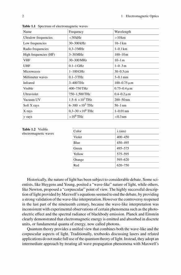
1.1 Spectrum of Electromagnetic Waves
The typical nomenclature of electromagnetic waves is given in Table1.1, along withthe wavelength ranges associated with the different spectral bands. The field ofPhotonics covers the infrared, visible, and ultraviolet wavelength ranges.
The term “light” is born to indicate electromagnetic radiation having wavelengthwithin the interval 0.4–0.75µm,which is the interval spannedby the radiation emittedby the sun. As a result of biological adaptation, this is also the wavelength range towhich the retina of our eyes is sensitive. In contemporary scientific terminology, theterm “light” is also applied to infrared and ultraviolet radiation.
In this text ν expresses the frequencyof light, and ismeasured in units of hertz (Hz).Alternatively, ω = 2πν, the angular frequency of light can be used, and is measuredin radians per second. The wavelength of light, expressed as λ, is usually measuredin micrometers/microns (1 µm = 10−6 m) or nanometers (1 nm = 10−9 m). Thespeed of light in vacuum is expressed as c, and is related to the wavelength andfrequency by c = λν. In general, the International System (SI) of units will be used.Appendix A gives the list of prefixes used to indicate multiples and submultiples ofthe fundamental units.
Table1.2 shows the wavelength ranges corresponding to different colors of visibleelectromagnetic waves.
© Springer International Publishing Switzerland 2016V. Degiorgio and I. Cristiani, Photonics, Undergraduate Lecture Notes in Physics,DOI 10.1007/978-3-319-20627-1_1
1
2 1 Electromagnetic Optics
Table 1.1 Spectrum of electromagnetic waves
Name Frequency Wavelength
Ultralow frequencies <30kHz >10km
Low frequencies 30–300kHz 10–1km
Radio frequencies 0.3–3MHz 1–0.1km
High frequencies (HF) 3–30MHz 100–10m
VHF 30–300MHz 10–1m
UHF 0.1–1GHz 1–0 .3m
Microwaves 1–100GHz 30–0.3cm
Millimeter waves 0.1–3THz 3–0.1mm
Infrared 3–400THz 100–0.75µm
Visible 400–750THz 0.75–0.4µm
Ultraviolet 750–1,500THz 0.4–0.2µm
Vacuum UV 1.5–6 ×10³ THz 200–50nm
Soft X rays 6–300 ×103 THz 50–1nm
X rays 0.3–30×106 THz 1–0.01nm
γ rays >106 THz <0.3nm
Table 1.2 Visibleelectromagnetic waves
Color λ (nm)
Violet 400–450
Blue 450–495
Green 495–575
Yellow 575–595
Orange 595–620
Red 620–750
Historically, the nature of light has been subject to considerable debate. Some sci-entists, like Huygens and Young, posited a “wave-like” nature of light, while others,like Newton, proposed a “corpuscular” point of view. The highly successful descrip-tion of light provided byMaxwell’s equations seemed to end the debate, by providinga strong validation of thewave-like interpretation. However the controversy reopenedin the last part of the nineteenth century, because the wave-like interpretation wasinconsistent with experimental observations of certain phenomena such as the photo-electric effect and the spectral radiance of blackbody emission. Planck and Einsteinclearly demonstrated that electromagnetic energy is emitted and absorbed in discreteunits, or fundamental quanta of energy, now called photons.
Quantum theory provides a unified view that combines both the wave-like and thecorpuscular aspects of light. Traditionally, textbooks discussing lasers and relatedapplications do notmake full use of the quantum theory of light. Instead, they adopt anintermediate approach by treating all wave propagation phenomena with Maxwell’s

1.1 Spectrum of Electromagnetic Waves 3
equations, and introducing light quanta only when discussing absorption and emis-sion phenomena. This intermediate approach is also used in this book, as it is partic-ularly suited to a concise introduction to Photonics.
Considering a monochromatic plane wave with frequency ν and wave vector k,the corresponding photon is a quasi-particle without mass, with an energy of hν
and a momentum of hk/(2π). The universal constant, h, called Planck constant,has value 6.55 × 1034 J·s. Usually the photon energy is conveniently expressed inunits of electronvolt (eV): 1eV is the energy acquired by an electron (electric chargee = 1.6 × 10⁻¹⁹ C) when it is accelerated by a potential difference of 1V, and so1 eV = 1.6 × 10⁻¹⁹ J.
1.2 Electromagnetic Waves in Vacuum
The vacuum propagation of electromagnetic waves is described by Maxwell’sequations:
∇ · E = 0, (1.1)
∇ · B = 0, (1.2)
∇ × B = εoμo∂E∂t
, (1.3)
∇ × E = −∂B∂t
, (1.4)
where E is the electric field (measured in V/m), and B is the magnetic induction(measured in T ). The constant εo = 8.854 × 10⁻¹² F/m is called the dielectricconstant (or electric permittivity) of free space, and μo = 4π × 10−7 H/m is thevacuum magnetic permeability.
Recalling a general property of differential operators:
∇ × (∇ × E) = ∇(∇ · E) − ∇2E, (1.5)
taking the rotor of both members of (1.4), and using (1.1), it is found that:
∇ × (∇ × E) = −∇2E = −∂(∇ × B)
∂t. (1.6)
By using (1.3), one obtains a single equation, called the wave equation, in whichthe unknown function is the electric field:
∇2E = 1
c2∂2E∂t2
, (1.7)

4 1 Electromagnetic Optics
where c = (εoμo)−1/2 is the propagation velocity of the electromagnetic wave. It
can be shown that B satisfies an equation that is identical to (1.7).The wave described by (1.7) transports both energy and momentum. The flow of
electromagnetic energy is governed by the Poynting vector, defined as:
SP = E × H, (1.8)
where H = B/μo is the magnetic field (units: A/m). The modulus of SP, which hasdimension W/m2, represents the power per unit area transported by the electromag-netic wave.
An important particular solution of (1.7) is the monochromatic plane wave:
E = Eo cos (ωt − k · r + φ) = Eo Re{exp[−i(ωt − k · r + φ])}, (1.9)
where k is the propagation vector, with modulus k = 2π/λ = ω/c, and φ is aconstant phase that can always be put equal to 0 by an appropriate choice of thetime origin. The wave described by (1.9) generates plane equal-phase surfaces (alsocalled wavefronts) that are perpendicular to k.
By substituting (1.9) into (1.1), one finds: ik ·E = 0, that is: E ⊥ k. Analogously,from (1.2) one derives B ⊥ k. In addition, Maxwell equations say that E ⊥ B,that E and B have the same phase, and that B = √
εoμo E . Summarizing, theelectromagnetic plane wave is a transverse wave, in which electric and magneticfield vectors are mutually orthogonal and lie in a plane that is perpendicular to thepropagation direction.
The Poynting vector of the plane wave is parallel to the propagation vector k. Byinserting (1.9) into (1.8), the following expression is found:
SP = cεo E2o
kkcos2(ωt − k · r + φ). (1.10)
Optical fields oscillate at very high frequencies. For instance, at the wavelengthλ = 1µm, the corresponding oscillation period is T = λ/c = 3.3×10⁻¹⁵ s = 3.3 fs.In most cases it is more significant to consider time averaged quantities instead ofinstantaneous values. To this end, it is useful to recall a general property of sinusoidalfunctions: given two functions oscillating at the same frequency, a(t) = A cos(ωt +φA) and b(t) = B cos(ωt + φB), the time average of the product is:
〈a(t)b(t)〉 = 1
2AB cos(φA − φB). (1.11)
Using (1.11), it is found that the time-average of the modulus of SP, which is theintensity of the wave, is given by:
I = cεo E2
o
2. (1.12)

1.2 Electromagnetic Waves in Vacuum 5
As shown in (1.9), the electric field can be described by using complex exponen-tials of the type E = Eoexp[−i(ωt − k · r + φ)] instead of real sinusoidal functions.In this text the exponential notation will be often used to simplify the calculations. Inany case it should never be forgotten that only the real part of the complex exponentialcorresponds to the real electric field.
1.3 Polarization of Light
The direction of polarization of an electromagnetic wave is the direction of the vectorE. Assume that a plane wave is propagating in the z direction. The electric field isoriented in the x-y plane. Its x and y components are both sinusoidal functions oftime:
Ex = Exo cos(ωt − kz), (1.13)
Ey = Eyo cos(ωt − kz + φ), (1.14)
where φ is the phase shift between the two components. Putting X = Ex/Exo =cos(ωt −kz) and Y = Ey/Eyo = cos(ωt −kz +φ) = cos(ωt −kz) cosφ−sin(ωt −kz) sin φ, it is possible to write an implicit equation containing X and Y , but not thespatio-temporal coordinates:
X cosφ − Y =√1 − X2 sin φ. (1.15)
By squaring both sides of (1.15) one obtains:
X2 + Y 2 − 2XY cosφ = sin2 φ, (1.16)
hence:E2
x
E2xo
+ E2y
E2yo
− 2Ex Ey
Exo Eyocosφ = sin2 φ. (1.17)
Equation (1.17) describes the trajectory of the endpoint of the vector E in theplane x-y. The motion is periodic in time, with period T = 1/ν. In the general case,the trajectory is an ellipse, as shown in Fig. 1.1, and the wave is said to be ellipticallypolarized. In the particular case of φ = 0, the ellipse reduces to a straight line, i.e.,the direction of the electric field vector does not change with time. The straight lineforms an angle α with the x axis, given by the relation tan(α) = Eyo/Exo. Linearpolarization is also obtained when φ = π , in this case the polarization directionforms an angle −α with the y axis.
In the case φ = ±π/2 and Exo = Eyo, the endpoint of the vector E sketches outa circle in one optical period, and so the wave is said to be circularly polarized. Therotation of E can be clockwise, if φ = π/2, or anti-clockwise, if φ = −π/2.

6 1 Electromagnetic Optics
Fig. 1.1 Polarization of electromagnetic waves for different values of the phase shift between Exand Ey
Ageneric polarization state can also be described as a superposition of two circularpolarizations, each having a different amplitude and phase. If the two amplitudesare different the resulting polarization is elliptical. If the amplitudes are equal, thesuperposition corresponds to a linear polarization, having direction controlled by thephase shift between the two circular polarizations.
It is usually said that the light emitted by the Sun and by conventional sources isunpolarized. What is meant here is that the direction of the electric field observed ina given point is an essentially random function of time
1.4 Paraxial Approximation
Representing the field of the monochromatic wave as: E(r, t) = E(r)exp(−iωt),and substituting this expression into the wave equation (1.7), allows the so-calledHelmholtz equation to be obtained:

1.4 Paraxial Approximation 7
(∇2 + k2)E(r) = 0 (1.18)
In real situations one never dealswith ideal planewaves, but ratherwith collimatedbeams, like those emitted by lasers. It is therefore useful to develop approximatedtreatments applicable to light beams possessing a relatively small distribution ofwave vectors. Since the discussion will only concern the spatial properties of mono-chromatic fields, the time-dependent term exp(−iωt) will be omitted from now onin this chapter inside all the expressions involving the electric field.
Considering a light beam that travels along the z axis, and substituting the fol-lowing expression for the electric field inside (1.18):
E(x, y, z) = U (x, y, z)exp(ikz), (1.19)
the Helmholtz equation becomes:
∂2U
∂x2+ ∂2U
∂y2+ ∂2U
∂z2+ 2ik
∂U
∂z= 0. (1.20)
It is now assumed that U is a slowly varying function of z, where slowly varyingmeans that the spatial scale over which U has significant variations is much biggerthan the wavelength λ, as qualitatively shown in Fig. 1.2. Mathematically, this isequivalent to state that:
dU
dz� kU. (1.21)
A consequence of (1.21) is that the second derivative of U with respect to z ismuch smaller than kdU/dz, and so it can be neglected inside (1.20), obtaining theso-called paraxial equation:
∂2U
∂x2+ ∂2U
∂y2+ 2ik
∂U
∂z= 0. (1.22)
Fig. 1.2 Paraxial approximation

8 1 Electromagnetic Optics
In order to better clarify the meaning of the paraxial approximation, it is useful toconsider the simple case of a wave made by the superposition of three plane waves,one having vector k directed along the z axis, the two others with k laying in theplane x-z and forming angles ±α with the z axis. By assuming that the three planewaves have the same amplitude Uo, U (x, y, z) can be written as:
U (x, y, z) = Uo{1 + exp[ik(cosα − 1)z][exp(ikx sin α) + exp(−ikx sin α)]}.
The first derivative with respect to z is:
dU
dz= ik(cosα − 1)(U − Uo).
If α is small, then the quantity cosα − 1 is also small with respect to 1. Thereforeit is demonstrated that:
∣∣∣dU
dz
∣∣∣ � |k(U − Uo)| < |kU |.
1.4.1 Spherical Waves
An important particular solution of the wave equation (1.7) is a wave with sphericalwavefronts, whose electric field, in scalar form, is expressed as:
E = Ao
|r − ro|exp(ik|r − ro|) (1.23)
The origin of the spherical wave is at point ro having coordinates xo, yo, zo.Putting the origin on the z axis means xo = yo = 0, and the distance |r − ro| is givenby:
|r − ro| =√
x2 + y2 + (z − zo)2
= (z − zo)
√
1 + x2 + y2
(z − zo)2(1.24)
The paraxial approximation is applied to (1.24) by assuming that the fractionappearing under the square root in the last term is small compared to 1. By expandingthe square root in a power series, and keeping only the first-order term, the followingexpression is derived:
|r − ro| ≈ (z − zo)
[1 + x2 + y2
2(z − zo)2
]. (1.25)

1.4 Paraxial Approximation 9
Fig. 1.3 Convention for the sign of the radius of curvature of the spherical wave
To use (1.25) instead of (1.24) is analogous to approximating the spherical wave-front with a paraboloid. The validity of (1.25) is clearly limited to situations in whichonly that part of the wavefront for which the distance from the z axis is much lessthan z − zo is considered.
Calling R(z) = z−zo the radius of curvature of the wavefront allows the complexamplitude of the electric field associated to the spherical wave to be written as:
U (x, y, z) = Ao
R(z)exp
(ik
x2 + y2
2R(z)
). (1.26)
The radius of curvature can be positive or negative: the chosen convention (shownin Fig. 1.3) being that positive R indicates a wavefront having convexity orientedtoward positive z, i.e. when the wave is diverging.
1.4.2 Gaussian Spherical Waves
As will be shown in Chap.3, the beam emitted by a laser can usually be described asa spherical wave presenting a Gaussian amplitude distribution in the x-y plane. Theelectric field of this Gaussian spherical wave is:
U (x, y, z) = A(z)exp
[− x2 + y2
w2
]exp
[ik(x2 + y2)
2R
]
= A(z)exp
[ik(x2 + y2)
2q
], (1.27)
where w is the distance from the z axis at which the field amplitude is reduced by afactor 1/e. The parameter w can be called radius of the Gaussian wave.

10 1 Electromagnetic Optics
The quantity q appearing in the right-hand side of (1.27) is called the complexradius of curvature. It is defined by the expression:
1
q= 1
R+ i
λ
πw2 (1.28)
By substituting (1.27) inside (1.22), one obtains:
[k2
q2
(dq
dz− 1
)(x2 + y2
) + 2ik
q
(q
A
d A
dz+ 1
)]A(z) = 0 (1.29)
Equation (1.29) can be satisfied for all possible values of x and y provided that:
dq
dz= 1 ; d A(z)
dz= − A(z)
q(z). (1.30)
By using the initial conditions q(zo) = qo, A(zo) = Ao, the following solutionsto (1.30) are found:
q(z) = qo + z − zo ; A(z)
Ao= qo
q(z). (1.31)
It is therefore demonstrated that the Gaussian spherical wave is a solution of theparaxial equation. This means that the wave does not change its functional formunder propagation. What happens is that the amplitude A(z) and the complex radiusof curvature q(z) change with z following simple algebraic laws. In particular theevolution of q(z) is identical to that of the radius of curvature of the spherical wave.
The case of a Gaussian spherical wave having a planar wavefront at z = 0 is nowconsidered. If the radius of curvature of the wavefront is infinite for z = 0, then thereciprocal of the complex radius of curvature at z = 0, as derived from (1.28), is:1/qo = iλ/(πw2
o), where wo is the beam radius at z = 0. The field distribution atz = 0 is:
U (xo, yo, 0) = Aoexp
[ik(x2o + y2o )
2qo
]= Aoexp
[− x2o + y2o
w2o
]. (1.32)
Having assigned U (xo, yo, 0), the field distribution at the generic coordinate zis immediately derived by using the two conditions of (1.31) that describe how theamplitude and the complex radius of curvature are modified during the propagationalong the z axis. Note that the propagation problem is solved through the algebraicrelations (1.31) without making use of the differential equation (1.22). It is found:
U (x, y, z) = Aoqo
qo + zexp
[ik(x2 + y2)
2(qo + z)
], (1.33)

1.4 Paraxial Approximation 11
which can also be written as:
U (x, y, z) = Aowo
w(z)exp [−iψ(z)]exp
[ik(x2 + y2)
2q(z)
], (1.34)
where
q(z) = z + qo = z − iπw2o
λ, (1.35)
w(z) = wo
√
1 +(
λz
πw2o
)2
= wo
√
1 +(
z
zR
)2
, (1.36)
and
ψ(z) = arctan( λz
πw2o
)= arctan
( z
zR
). (1.37)
The quantity zR is called Rayleigh length, and is defined as follows:
zR = πw2o
λ. (1.38)
The behavior of the beam radius w(z) is reported in Fig. 1.4. It is seen that theGaussian spherical wave has the minimum radius at the position (usually calledbeam waist) in which its wavefront is planar. The Rayleigh length represents thepropagation distance at which the beam radius becomes larger than wo by a factor√2. The beam radius is slowly growing for z ≤ zR and tends to grow linearly as
z zR .Equation (1.34) indicates that the propagating Gaussian spherical wave acquires,
with respect to the plane wave, an additional phase delay of ψ(z) that, according to(1.37), varies from −π/2 for z � zR to π/2 for z zR , as shown in Fig. 1.5.
By using (1.28) and (1.35) the z-dependence of the radius of curvature of thewavefront is derived:
Fig. 1.4 Gaussian sphericalwave: behavior of the beamradius, w(z), as a function ofthe propagation distance

12 1 Electromagnetic Optics
Fig. 1.5 Gaussian sphericalwave: behavior of theadditional phase delay, ψ(z),as a function of thepropagation distance
Fig. 1.6 Gaussian sphericalwave: behavior of the radiusof curvature of thewavefront, R(z), as afunction of the propagationdistance
R(z) = z + 1
z
(πw2o
λ
)2 = z + zR2
z. (1.39)
The behavior of R(z) is illustrated in Fig. 1.6.It is interesting to discuss the behavior of the Gaussian spherical wave at distances
from the waist plane much larger than the Rayleigh length. If z zR , one findsfrom (1.36):
w(z) ≈ λz
πwo. (1.40)
Since the beam radius grows proportionally to distance, most of the propagatingpower is concentrated inside a cone having the aperture:
θo = λ
πwo. (1.41)
1.4 Paraxial Approximation 13
The angle θo is the divergence angle of the beam. Equation (1.41) expresses avery general concept for wave propagation: the finite transversal size of the beamis necessarily associated to an angular spread of the wave vector directions. Apartfrom a numerical factor of the order of one, the divergence angle is given by the ratiobetween wavelength and transversal size of the light beam. As it will be seen in thefollowing sections, the same result is found in the classical diffraction problem, inwhich a planewave crossing a screenwith a circular aperture of radius D/2 generatesa beam with an angular spread ≈2λ/D.
To complete the discussion concerning the behavior at z zR , (1.39) shows thatR(z) approaches the value of z, that is, it tends towards the value expected for aspherical wave centered at z = 0.
The paraxial equation admits other beam-like solutions that, like the sphericalGaussian wave, do not change their shape during free propagation. An interestingfamily of such solutions is that of Hermite-Gauss spherical waves, whose amplitude,in Cartesian coordinates, is the product of a Gaussian function times two Hermitepolynomials:
U (x, y, z) = Aowo
w(z)exp [−i(l + m + 1)ψ(z)]
exp[ik(x2 + y2)
2q(z)
]Hl
(√2
x
w(z)
)Hm
(√2
y
w(z)
), (1.42)
where the Hermite polynomial of order n is defined as
Hn(ξ) = exp(ξ2)(−1)n dn
dξnexp(−ξ2). (1.43)
Applying (1.43) to generate, as an example, the polynomials of order 0, 1, 2, it isfound:
H0(ξ) = 1; H1(ξ) = 2ξ ; H2(ξ) = 4ξ2 − 2. (1.44)
The Hermite-Gaussian beam of order (0,0) is the simple Gaussian beam. As willbe seen in Chap.3, the Hermite-Gaussian beams are useful to describe the fielddistribution inside laser cavities.
To summarize, the treatment developed in this section has demonstrated thatGaussian spherical waves have propagation properties similar to those of sphericalwaves in the geometrical optics approach. However one important difference is thatall the formulas developed in this section include the effects due to diffraction.
1.5 Diffraction Fresnel Approximation
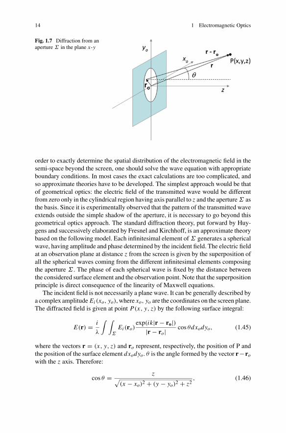
The classical diffraction theory concerns the situation illustrated in the scheme ofFig. 1.7. A monochromatic plane wave, with propagation vector k parallel to the zaxis is transmitted through an apertureΣ in an opaque screen laying on plane x-y. In
14 1 Electromagnetic Optics
Fig. 1.7 Diffraction from anaperture Σ in the plane x-y
order to exactly determine the spatial distribution of the electromagnetic field in thesemi-space beyond the screen, one should solve the wave equation with appropriateboundary conditions. In most cases the exact calculations are too complicated, andso approximate theories have to be developed. The simplest approach would be thatof geometrical optics: the electric field of the transmitted wave would be differentfrom zero only in the cylindrical region having axis parallel to z and the apertureΣ asthe basis. Since it is experimentally observed that the pattern of the transmitted waveextends outside the simple shadow of the aperture, it is necessary to go beyond thisgeometrical optics approach. The standard diffraction theory, put forward by Huy-gens and successively elaborated by Fresnel and Kirchhoff, is an approximate theorybased on the following model. Each infinitesimal element ofΣ generates a sphericalwave, having amplitude and phase determined by the incident field. The electric fieldat an observation plane at distance z from the screen is given by the superposition ofall the spherical waves coming from the different infinitesimal elements composingthe aperture Σ . The phase of each spherical wave is fixed by the distance betweenthe considered surface element and the observation point. Note that the superpositionprinciple is direct consequence of the linearity of Maxwell equations.
The incident field is not necessarily a plane wave. It can be generally described bya complex amplitude Ei (xo, yo), where xo, yo are the coordinates on the screen plane.The diffracted field is given at point P(x, y, z) by the following surface integral:
E(r) = i
λ
∫ ∫
Σ
Ei (ro)exp(ik|r − ro|)
|r − ro| cos θdxodyo, (1.45)
where the vectors r = (x, y, z) and ro represent, respectively, the position of P andthe position of the surface element dxodyo. θ is the angle formed by the vector r−ro
with the z axis. Therefore:
cos θ = z√
(x − xo)2 + (y − yo)2 + z2, (1.46)

1.5 Diffraction Fresnel Approximation 15
and
|r − ro| =√
(x − xo)2 + (y − yo)2 + z2 = z
√
1 + (x − xo)2 + (y − yo)2
z2.
(1.47)The imaginary unit i placed in front of the integral (1.45) indicates that the spher-
ical wave coming from the generic surface element is phase-shifted by π/2 withrespect to the incident wave. Provided that the diffracted field is evaluated at anobservation point satisfying the condition z λ, the integral (1.45) represents agood approximation to the exact solution.
The integral (1.45) can be extended to thewhole plane x-y by inserting a transmis-sion function τ(xo, yo), which takes the value 1 inside the aperture Σ and 0 outside.The introduction of τ(xo, yo) allows for generalizing the treatment to partially trans-mitting screens and/or phase screens, in which case τ becomes a complex quantitywith a modulus taking intermediate values between 0 and 1.
The generalized diffraction integral is written as:
E(r) = i
λ
∫ ∞
−∞dxo
∫ ∞
−∞τ(xo, yo)Ei (ro)
exp(ik|r − ro|)|r − ro| cos θdyo. (1.48)
Diffraction theory, as expressed in (1.48), constitutes an approximate propagationtheory of electromagnetic waves. In fact, once a field distribution is defined on theplane z = 0 immediately beyond the screen plane, the integral (1.48) gives the fielddistribution at any later generic plane z.
In many cases it is useful to consider the Fresnel approximation, which assumesthat the angle θ is small for all the considered points. Mathematically, this is equiva-lent to the assumption that the fraction appearing inside the square root in the right-hand member of (1.47) is small compared to 1. By truncating the series expansionof (1.47) at the first order, the following expression is obtained:
|r − ro| ≈ z
[1 + (x − xo)
2 + (y − yo)2
2z2
]. (1.49)
Considering the fraction inside the integral (1.48), the approximation |r−ro| = zcan be used for the denominator, but not for the numerator. In general, in the case ofan exponential of the type exp[i(A + A1)], the assumption that A1 is much smallerthan A is not in itself a sufficient condition to neglect A1. Since the exponential isa periodic function with period 2π , A1 can be neglected only if it is much smallerthan 2π .
By substituting (1.49) inside (1.48), and putting cos θ = 1, the diffraction integralunder the Fresnel approximation becomes:

16 1 Electromagnetic Optics
E(r) = i exp(ikz)
λz
∫ ∞
−∞dxo
∫ ∞
−∞τ(xo, yo)Ei (ro)exp
{ik
2z[(x − xo)
2 + (y − yo)2]
}dyo (1.50)
The integral (1.50) is a convolution of a complex Gaussian nucleus with the fielddistribution present in the plane immediately after the screen.
The Fresnel approximation is valid provided that the first neglected term at theexponent of the complex exponential is small compared to 2π :
k(x − xo)4
4z3� 2π. (1.51)
Considering, as an example, a circular aperture of diameter D, (1.51) is verified if:
z3 D4
λ. (1.52)
However, it should bementioned that the comparison of the Fresnel approximationwith exact numerical results shows a good agreement even in cases in which thecondition (1.52) is not fully satisfied.
The Fresnel approximation is now applied to describe the free propagation of aGaussian spherical wave. It is assumed that the wave has its waist on the plane z = 0.This means that the radius of curvature of the wavefront is infinite at z = 0, and thus:1/qo = iλ/(πw2
o), where wo is the beam radius at z = 0. The field distribution atz = 0 is:
Ei (xo, yo) = Aoexp
[ik(x2o + y2o )
2qo
]. (1.53)
The field distribution at the generic plane z is derived by inserting (1.53) into(1.50), and putting τ(xo, yo) = 1. The diffraction integral is calculated by separatingthe integration variables. The result is:
E(x, y, z) = Aoi exp(ikz)
λzJ (x, z)J (y, z), (1.54)
where:
J (x, z) =∫ ∞
−∞exp
[ik(x − xo)
2
2z
]exp
[ikx2o2qo
]dxo. (1.55)
Recalling that:
∫ ∞
−∞exp
(− x2
w2
)dx =
∫ ∞
−∞exp
[− (x − a)2
w2
]dx = √
π w, (1.56)
1.5 Diffraction Fresnel Approximation 17
where a is an arbitrary constant, the integral (1.55) is readily calculated by expressingthe integrand function as a displaced Gaussian function:
J (x, z) =∫ ∞−∞
exp
[ik
2
(qo + z
qozx2o − 2xxo
z+ x2
z
)]
dxo
= exp
[ikx2
2(qo + z)
] ∫ ∞∞
exp
{ik(qo + z)
2qoz
[xo − qox
qo + z
]2}
dxo. (1.57)
The final expression of E(x, y, z) is:
E(x, y, z) = Aoqo
qo + zeikzexp
[ik(x2 + y2)
2(qo + z)
](1.58)
This result, which exactly matches (1.33), is not surprising because the Fresnelapproximation of the diffraction integral is essentially equivalent to the paraxialapproximation.
1.6 Fraunhofer Diffraction
A further simplification to diffraction theory is introduced by the Fraunhofer approx-imation, which consists of neglecting the terms quadratic in xo and yo in the exponentinside (1.50). This simplification is valid when the terms to be neglected are smallin comparison to π . This requires:
z (x2o + y2o )
λ. (1.59)
For a circular aperture with diameter D, the maximum value of x2o + y2o is D2/4,therefore the condition (1.59) becomes:
z D2
4λ. (1.60)
In most practical cases it may be very difficult to satisfy such a condition. If, forinstance, λ = 0.6µm, and D = 5cm, then (1.60) requires z 3km. This exampleexplainswhy the Fraunhofer approximation is also called the far-field approximation.As it will be described in the next chapter, a converging lens can be used to bringthe far field into the lens focal plane. By exploiting this possibility, the Fraunhoferapproximation can be utilized in various applications.

18 1 Electromagnetic Optics
Fig. 1.8 Decomposition of an optical wave into plane waves
The integral (1.50), as written in the Fraunhofer approximation, becomes:
E(x, y, z) = i exp(ikz)
λzexp
[ik
2z(x2 + y2)
]
∫ ∞
−∞dxo
∫ ∞
−∞τ(xo, yo)Ei (xo, yo)exp[−i(k/z)(xxo + yyo)]dyo. (1.61)
Apart from amultiplicative factor, the field distribution E(x, y, z) given by (1.61)is the two-dimensional Fourier transform of the distribution at z = 0. The twovariables that are conjugated to xo, yo are: fx = x/(λz) and fy = y/(λz). These are
the components of the spatial frequency f, having modulus f =√
f 2x + f 2y .
In order to grasp the physical meaning of the quantity f, it should be recalled thatthe field τ Ei present immediately after the plane xo-yo can always be described as asuperposition of plane waves. As shown in Fig. 1.8, each plane wave is characterizedby a different vectork. The direction ofk is determinedby assigning the two anglesαx
andαy , formedbykwith the axes x and y.Once givenαx andαy , the angleαz betweenk and z may be calculated from the relation: cos2 αx + cos2 αy + cos2 αz = 1. Forevery pair of values of αx and αy , there corresponds a spatial frequency f withcomponents fx = λ−1 cosαx e fy = λ−1 cosαy . The modulus of f is:
f =√1 − cos2 αz
λ= sin αz
λ. (1.62)
The term “spatial frequency” comes from the fact that f −1 is the spacing (spatialperiod) of the projected wavefronts on the plane xo-yo, as shown in Fig. 1.8. If theplane wave propagates perpendicularly to z, αz = π/2 and f −1 = λ. If k is parallelto z, αz = 0, and f −1 becomes infinite.
Equation (1.62) indicates that the plane wave characterized by αx and αy is repre-sented on the plane z in the far field by the point x = fxλz and y = fyλz. In the casewhere the field incident on the screen is a plane wave directed along z, E(x, y, z) issimply the Fourier transform of the transmission function τ(xo, yo).

1.6 Fraunhofer Diffraction 19
1.6.1 Rectangular and Circular Apertures
As a first example of the application of the Fraunhofer approximation, a rectangularaperture illuminated by a plane wave propagating along z is here considered. Theassumed transmission function is:
τ(xo, yo) = rect
(xo
Lx
)rect
(yo
L y
), (1.63)
where rect (x) is unitary inside the interval −0.5 ≤ x ≤ 0.5 and is 0 elsewhere.The transform of (1.63) is: F{τ(xo, yo)} = Lx L y sin c(π Lx fx ) sin c(π L y fy)wheresinc(x) = sinx/x . By substitution into (1.61), it is found:
E(x, y, z) = Aoi exp(ikz)
λzexp
[ik
2z(x2 + y2)
]Lx L y sinc
(π
x Lx
λz
)sinc
(π
yL y
λz
),
(1.64)
where Ao is the amplitude of the incident wave.Figure1.9 shows the image of the diffractedwave, whereas Fig. 1.10 illustrates the
transversal behavior of the optical intensity I (x, y, z), proportional to |E(x, y, z)|2,along the x axis. While the wave incident on the aperture consists only of the prop-agation vector parallel to z, the diffracted wave has a distribution in k vectors thatbecomes wider as the size of the aperture reduces. In fact, the width of the maindiffraction lobe, evaluated along x as the distance between the first two zeroes, is:Δx = λz/Lx , or, in other terms, the angular aperture of the main diffraction lobe isλ/(2Lx ).
As a second example, consider a circular aperture having a transmission function:
τ(xo, yo) = circ(ro
R
), (1.65)
Fig. 1.9 Fraunhoferdiffraction from a squareaperture: image of thediffracted wave

20 1 Electromagnetic Optics
Fig. 1.10 Fraunhoferdiffraction from a squareaperture: intensity versus x
where circ(ro/R) is equal to 1 inside the circle of radius R and 0 elsewhere. Using(1.61), the diffracted field is found to be:
E(r) = Aoi exp(ikz)
λzexp
[ik
2zr2
]R2 J1[r R/(λz)]
r R/(λz), (1.66)
where J1 is the order 1 Bessel function. The intensity distribution I (r), proportionalto |E(r)|2, is called Airy function. Figure1.11 shows the image of the diffractedwave, and Fig. 1.12 gives the behavior of I (r). The radius corresponding to the firstzero is: 0.61 λz/R. Here again it is found that the angular spread of the diffractedwave is of the order of the ratio between wavelength and size of the aperture.
Fig. 1.11 Fraunhoferdiffraction from a circularaperture: image of thediffracted wave

1.6 Fraunhofer Diffraction 21
Fig. 1.12 Fraunhoferdiffraction from a circularaperture: behavior of thediffracted intensity I (r) as afunction of the distance fromthe z axis
1.6.2 Periodical Transmission Function
Consider a plane wave propagating along z that illuminates a square aperture ofside L that has a transmission function varying sinusoidally along x , with periodd = 1/ fo:
τ(xo, yo) = 1 + m cos (2π foxo)
2rect
( xo
L
)rect
( yo
L
), (1.67)
where the parameter m is the modulation depth.The Fourier transform of the fraction that appears in the right-hand member of
(1.67) is:
F
{1 + m cos 2π foxo
2
}= 1
2δ( fx , fy) + m
4δ( fx + fo, fy) + m
4δ( fx − fo, fy),
(1.68)where δ(x) is the Dirac delta function, which is infinite at x = 0 and zero elsewhere.Recalling that the Fourier transform of the product of two functions is the convolutionof the two transforms, the far-field diffraction pattern is given by:
E(x, y, z) = Aoi L2exp(ikz)
2λzexp
[ik
2z(x2 + y2)
]sinc
(π
yL
λz
)
{sinc
(π
x L
λz
)+ m
2sinc
[π
L
λz(x + foλz)
]+ m
2sinc
[π
L
λz(x − foλz)
]}.
(1.69)
The behavior of the diffracted intensity as a function of x is reported in Fig. 1.13.The three peaks correspond to three diffracted waves. The central peak, i.e., the zero-th order wave, represents the fraction of incident wave that is still propagating along

22 1 Electromagnetic Optics
Fig. 1.13 Diffractedintensity from a periodicaltransmission function
z, with a distribution of k vectors arising from the diffracting effect due to the finitesize of the aperture. The lateral peaks, symmetrically positioned around the centralone, represent waves with propagation vectors laying in the x-z plane and formingthe angles±λ/d with the z axis. These two waves constitute the diffraction order+1and −1, respectively. The spatial separation between order 0 and order ±1 is foλz,which means that the angular separation is ± foλ. The two first-order diffractionpeaks are broadened, like the central peak, because of the finite size of the aperture.
At this point it is easy to understand what happens if the transmission functionτ(xo, yo) is a periodic function with a square profile instead of a sinusoidal profile.The square profile contains, with decreasing amplitude, all the harmonics. As aconsequence, diffracted waves with orders higher than 1 are generated.
An other interesting case is that of a phase screen, having a transmission functionthat is a complex function with unitary modulus and sinusoidal phase:
τ(xo, yo) = exp
[im sin (2π foxo)
2
]rect
( xo
L
)rect
( yo
L
). (1.70)
Such a transfer function can be realized by using a transparent material with aperiodic modulation of index of refraction or of thickness along the coordinate xo.Recalling that:
exp
[im sin 2π foxo
2
]=
∞∑
q=−∞Jq
(m
2
)exp(i2πq foxo), (1.71)
where Jq is the q-th order first-type Bessel function, and using the convolutiontheorem, one finds:

1.6 Fraunhofer Diffraction 23
E(x, y, z) = Aoi L2exp(ikz)
2λzexp
[ ik
2z(x2 + y2)
]sin c
(π
yL
λz
)
∞∑
q=−∞Jq
(m
2
)sin c
[π L
λz(x − q foλz)
](1.72)
Equation (1.72) shows that the sinusoidal phase profile presents, in principle, allpossible diffraction orders. The amplitude of the generic order q is determined bythe value of the corresponding Bessel function for the argument m/2. Note that thetransmitted beam (that is, the zero-th order) can be totally suppressed in the particularcase of m/2 coinciding with a zero of J0.
As it will be seen in the next chapter, the diffraction from periodical transmissionprofiles has important applications to spectral measurements performed by usinggratings. The Fraunhofer approximation allows calculating not only the geometricalproperties, but also the power partitioning over the various diffraction orders of thegrating.
Problems
1.1 Consider the plane electromagnetic wave whose electric field is given by theexpressions (in SI units) Ex = 0, Ey = 200 cos[12π × 1014(t − z/c) + π/2], andEz = 0. What are the frequency, wavelength, direction of motion, amplitude, initialphase angle, and polarization of the wave?
1.2 Consider the plane electromagnetic wave in vacuumwhose electric field is givenby the expression E = Eo cos(ωt − kz). Assuming that the electric field amplitudeEo is 100V/m, calculate the amplitude of the magnetic field Bo in units of Tesla andthe intensity I in units of W/m2.
1.3 A plane electromagnetic wave propagating along the z axis has the followingelectric field components: Ex (t, z) = Eo cos(ωt − kz), and Ey(t, z) = √
3Eo cos(ωt − kz). Determine the angle formed by its polarization direction with the x axis.
1.4 A Gaussian beam at wavelength λ = 0.63µm has a radius at the beam waistof wo = 0.5mm. Calculate the beam radius w and the radius of curvature of thewavefront at a distance of 5 m from the beam waist.
1.5 A plane electromagnetic wave has wavelength λ = 500nm and a wave vectork that lies in the x-z plane, forming an angle αx = 60◦ with the x axis. Determinethe spatial frequency of the phase pattern on the z = 0 plane.
1.6 A plane wave of wavelength λ = 500nm illuminates a circular aperture havingdiameter D = 100µm. The diffraction pattern is observed on a screen placed at adistance of 30cm from the plane of the aperture. (i) check whether the condition forFraunhofer diffraction is satisfied; (ii) determine the position of the first zero of theAiry function.

Chapter 2Optical Components and Methods
Abstract In this chapter, after presenting Maxwell equations inside matter anddescribing reflection and refraction processes, the interaction of optical waves withsimple optical components such as mirrors, prisms, and lenses is examined. The dif-ferent methods for measuring the power spectrum of an optical beam are describedand compared in Sect. 2.3. In Sect. 2.4, after treating wave propagation in anisotropicmaterials, the methods used for fixing or modifying the polarization state of an opti-cal beam are presented. Finally, Sect. 2.5 introduces the important subject of opticalwaveguides.
2.1 Electromagnetic Waves in Matter
Inside a medium Maxwell’s equations take the following form:
∇ · D = ρ (2.1)
∇ · B = 0 (2.2)
∇ × H = J + ∂D∂t
(2.3)
∇ × E = −∂B∂t
, (2.4)
where D is the electric displacement vector (measured in units of C/m2). The quan-tities ρ and J are, respectively, the electric charge density (C/m3) and the currentdensity (A/m2). Here the treatment is limited to dielectric media, in which there areno free electric charges or currents, so that one can put J = ρ = 0.
The relations connecting D to E and B to H inside the medium become:
D = εoE + P (2.5)
B = μo(H + M). (2.6)
© Springer International Publishing Switzerland 2016V. Degiorgio and I. Cristiani, Photonics, Undergraduate Lecture Notes in Physics,DOI 10.1007/978-3-319-20627-1_2
25

26 2 Optical Components and Methods
The new vectors P and M are, respectively, the unit-volume electric polar-ization and the unit-volume magnetization inside the medium. In this book non-ferromagnetic media are only considered, and so it is possible to simplify the treat-ment by putting M = 0. The wave equation inside the medium is the following:
∇2E = 1
c2∂2E∂t2
+ μo∂2P∂t2
. (2.7)
In order to solve wave propagation problems, it is necessary to associate an equa-tion relating P to E to (2.7). It is useful to recall what is the physical meaning ofP. The medium is a collection of positively charged nuclei and negatively-chargedbound electrons. Under the action of an electric field the electron clouds are slightlydisplaced from their equilibrium position, so that a macroscopic electric dipole iscreated. Limiting the discussion to the time-dependence, it is clear that the mediumresponse to the application of an electric field cannot be instantaneous. Therefore, aconvolution relation should be used:
P(r, t) = εo
∫ t
−∞R(t − t ′)E(r, t ′)dt ′, (2.8)
where R(t − t ′) is the response function of the medium.The electric field E(r, t) associated with a generic light beam can always be
described as a weighted superposition of sinusoidal functions oscillating at differentfrequencies, as expressed by the integral:
E(r, t) = 1
2π
∫ ∞
−∞dωE(r, ω)exp(−iωt). (2.9)
The complex quantity E(r, ω) represents the weight of the component at angularfrequency ω. From a mathematical point of view, E(r, ω) is the Fourier transformof E(r, t).
The inversion of (2.9) gives:
E(r, ω) =∫ ∞
−∞dt E(r, t)exp(iωt). (2.10)
Recalling that the Fourier transform of the convolution of two functions is theproduct of their Fourier transforms, the Fourier transform of P(r, t) is expressed by:
P(r, ω) = εoχ(ω)E(r, ω), (2.11)
where χ(ω), called electric susceptibility, is given by:
χ(ω) =∫ ∞
−∞R(t)exp(iωt)dt . (2.12)

2.1 Electromagnetic Waves in Matter 27
By substituting (2.11) inside (2.5), it is found that the electric displacementD(r, ω), generated by a monochromatic electric field oscillating at the frequencyω, is proportional to E(r, ω):
D(r, ω) = εo(1 + χ)E(r, ω) = εoεr E(r, ω). (2.13)
The dimensionless constant εr is called relative dielectric constant or relativeelectric permittivity. The wave propagation velocity inside the dielectric medium is:
u = 1√εoεrμo
= c
n(2.14)
The quantity n, called index of refraction of the medium, is given by:
n = √εr = √
1 + χ. (2.15)
In the more general case, in which the relative magnetic permeability of thematerial, μr , may be different from 1, it is found that n = √
εrμr .Since the frequency of oscillation cannot change when the wave goes from one
medium to the other, the change of velocity is associatedwith a change ofwavelength.Specifically, if λ is the vacuum wavelength, then the wavelength inside a medium ofindex of refraction n is: λ′ = λ/n.
Since χ(ω) is frequency-dependent, also n(ω) = √1 + χ(ω) is frequency-
dependent. This phenomenon is called optical dispersion. As an example, over itstransparency window going from 0.35 to 2.3 µm, the index of refraction of theborosilicate glass called BK7 decreases monotonically from 1.54 at 0.35 µm to1.49 at 2.3 µm. This behavior is called normal dispersion. The dispersion is said tobe anomalous when the index of refraction increases as a function of wavelength.As it will be seen in Chap.6, the propagation of ultrashort light pulses is stronglyinfluenced by optical dispersion.
The electric field of the monochromatic plane wave inside the medium is stillgiven by (1.9). The only difference is that the modulus of the propagation vector isnow:
k = ω
u= ω
c
√1 + χ = ω
cn, (2.16)
and (1.12) becomes:
I = cεonE2
o
2. (2.17)
The propagation inside a medium with a real χ proceeds similarly to vacuumpropagation, the only difference being in the propagation velocity. However, if χ
is a complex quantity, then n is also complex, and can be written as: n = n′ +in′′. Assuming that a monochromatic plane wave, traveling along z, enters into themedium at z = 0, the electric field at the generic coordinate z is:

28 2 Optical Components and Methods
E = Eoexp{−i([ωt − (ω/c)(n′ + in′′)z]}. (2.18)
The intensity I (z), which is proportional to the square of the field modulus, isgiven by:
I (z) = Ioexp[−2(ω/c)n′′z] = Ioexp(−αz), (2.19)
where Io is the intensity at z = 0. Equation (2.19) shows that, if n′′ > 0, the waveintensity decays exponentially during propagation with an attenuation coefficient,α = 2(ω/c)n′′, proportional to the imaginary part of the refractive index. The atten-uation may be due to absorption or to scattering.
2.2 Reflection and Refraction
In this section the laws of reflection and refraction are introduced and applied todescribe the behavior of different optical components, such as mirrors and lenses.
2.2.1 Dielectric Interface
Amonochromatic plane wave is incident at the planar boundary between two dielec-tric media, characterized by refractive indices n1 and n2. According to the geometryshown in Fig. 2.1, the wave is coming from medium 1, and its wave-vector ki formsan angle θi with the normal to the boundary. The planar boundary is taken to coin-cide with the x-y plane, and ki lies on the y-z plane. The plane containing ki andthe normal to the planar boundary is known as the incidence plane. In the case ofFig. 2.1, y-z is the incidence plane.
Part of the wave will be reflected and part will be transmitted. Let θr and θt
be the reflection and transmission angles, respectively. By imposing the continuityconditions at the boundary for the tangential components of the electric andmagnetic
Fig. 2.1 Reflection andrefraction at a dielectricboundary

2.2 Reflection and Refraction 29
fields, it is possible to calculate the direction and the complex amplitude of thereflected and transmitted (also called refracted) waves.
It is useful to consider separately two different polarization states of the incidentwave: (a) a wave linearly polarized in a direction perpendicular to the incidenceplane, this is usually called σ case; (b) a wave linearly polarized in the incidenceplane, this is usually called π case. Any arbitrary polarization state of the incidentwave can always be described as a linear superposition of these two states.
• σ case.Putting |ki| = kon1, where ko = 2π/λ, the electric field of the incident wave is:
Ei = Eiexp(−iωt + iko yn1 sin θi + ikozn1 cos θi )x, (2.20)
where x is the unit vector directed along x . The electric fields Er and Et of thereflected and transmitted waves are written as:
Er = Erexp(−iωt + iko yn1 sin θr − ikozn1 cos θr )x, (2.21)
andEt = Etexp(−iωt + iko yn2 sin θt + ikozn2 cos θt )x. (2.22)
The continuity condition for the tangential component of the electric field at z = 0is:
Eiexp(iko yn1 sin θi )x + Erexp(iko yn1 sin θr )x = Etexp(iko yn2 sin θt )x. (2.23)
In order to satisfy (2.23) for any y, the reflection and transmission angles shouldsatisfy the relations:
θi = θr , (2.24)
andn1 sin θi = n2 sin θt . (2.25)
Equation (2.25) is known as Snell’s law.By using (2.24) and (2.25), (2.23) simply becomes
Ei + Er = Et (2.26)
In order to derive Er and Et , a second equation is needed besides that of (2.26).The continuity of the tangential component of the magnetic field is expressed as:
Hi cos θi − Hr cos θr = Ht cos θt (2.27)
Recalling that the electric field amplitude is related to themagnetic field amplitudeby the expression H = √
εrεo/μo E , (2.27) can be written as:

30 2 Optical Components and Methods
Ei cos θi − Er cos θr = n2
n1Et cos θt . (2.28)
The solution of the system of (2.26) and (2.28) can be presented in terms of thetransmission and reflection coefficients, τσ and ρσ , respectively:
τσ = Et
Ei= 2n1 cos θi
n1 cos θi + n2 cos θt= 2 sin θt cos θi
sin (θi + θt ), (2.29)
ρσ = Er
Ei= n1 cos θi − n2 cos θt
n1 cos θi + n2 cos θt= − sin (θi − θt )
sin (θi + θt ). (2.30)
If the incident beam is coming from medium 2, one can repeat the treatmentfinding two new coefficients, τ ′
σ and ρ′σ , related to the previous ones as follows:
ρ′σ = −ρσ ; τσ τ ′
σ = 1 − ρ2σ (2.31)
• π case.Following a treatment similar to that of the σ case, it is found that:
τπ = Et
Ei= 2n1 cos θi
n1 cos θt + n2 cos θi= 2 sin θt cos θi
sin (θi + θt ) cos (θi − θt ), (2.32)
ρπ = Er
Ei= n1 cos θt − n2 cos θi
n1 cos θt + n2 cos θi= − tan (θi − θt )
tan (θi + θt ). (2.33)
If the beam arrives at the boundary from medium 2, it is found that the relationsbetween the coefficients τ ′
π , ρ′π and the coefficients τπ and ρπ are identical to those
of (2.31).In the case of normal incidence, θi = θr = θt = 0, and ρσ coincides with ρπ :
ρσ (θi = 0) = ρπ(θi = 0) = −n2 − n1
n2 + n1. (2.34)
If n2 > n1, the field reflection coefficient is negative. This indicates that the phaseof Er is changed by π with respect to Ei . If n2 < n1, Er has the same phase as Ei .
In order to derive how the incident power splits between transmission and reflec-tion, it should be recalled that the power arriving on a generic surfaceΣ , is determinedas the time average of the flux of the Poynting vector through the surface. Projectingthe Poynting vector on the direction perpendicular to the surface, allows the followingexpression for Pi to be given:
Pi = (1/2)cεon1Σ |Ei |2 cos θi . (2.35)

2.2 Reflection and Refraction 31
Similarly, for the transmitted and reflected power:
Pr = (1/2)cεon1Σ |Er |2 cos θi Pt = (1/2)cεon2Σ |Et |2 cos θt . (2.36)
Therefore the reflectance R and the transmittance T are given by:
R = Pr
Pi= |Er |2
|Ei |2 = |ρ|2 (2.37)
T = Pt
Pi= |τ |2 n2 cos θt
n1 cos θi. (2.38)
Note that R + T = 1, whereas the sum |ρ|2 + |τ |2 is, in general, �= 1.The behavior of R as a function of θi depends on whether n1 is smaller or larger
than n2. Therefore the two cases are discussed separately.
• n1 < n2Considering, as an example, an air/glass boundary with a ratio n2/n1 = 1.5, the
behavior of Rπ e Rσ for a wave coming from air is illustrated in Fig. 2.2. At normalincidence (θi = 0), using (2.34), it is found that Rπ (θi = 0) = Rσ (θi = 0) = 0.04.The reflectance Rσ is monotonically increasing with θi reaching a value of 1 atθi = π/2 = 90◦. On the other hand, Rπ at first decreases till it vanishes at θi = θB ,and then increases, becoming equal to 1 at θi = π/2.
The angle θB is derived by noting that the reflection coefficient ρπ vanishes ifthe denominator of the fraction at right-hand side of (2.33) becomes infinite. Thishappens if: θi + θt = π/2. From this condition, by using Snell’s law, the followingexpression of θB , called Brewster’s angle, is derived:
Fig. 2.2 Reflectance versus incidence angle for n2/n1 = 1.5

32 2 Optical Components and Methods
tan θB = n2
n1(2.39)
As an example, if n2/n1 = 1.5, θB = 56◦, and Rσ (θB) = 0.147.In general, ρ is a complex quantity that can be written as ρ = √
R exp(iφ), whereφ is the phase shift of the reflected field with respect to the incident field. In the σ
case, (2.30) shows that φσ = π over the whole interval 0 ≤ θi ≤ π/2. In the π case,(2.33) indicates that φπ is equal to π within the interval 0 ≤ θi < θB , and vanishesfor θB ≤ θi ≤ π/2.
• n1 > n2In this case, Snell’s law indicates that θt is larger than θi . Therefore, as θi grows,
there will be an incidence angle, θc, smaller than π/2, at which θt becomes π/2. Ifθi ≥ θc there is no transmitted beam, and so the power reflection coefficient is equalto 1. The total reflection angle or limit angle, θc, is defined by the relation:
sin θc = n2/n1 (2.40)
Considering the glass/air interface, n1/n2 = 1.5, for which θc = 41.8◦, thebehavior of Rπ and Rσ is illustrated in Fig. 2.3. As in the previous case, Rπ vanishesat the Brewster angle, θB = 33.7◦.
The field reflection coefficient is a real quantity for θi ≤ θc. If θi > θc, cos θt
becomes imaginary:
cos θt =√1 − sin2 θt =
√
1 − n21
n22
sin2 θi = i
√n21
n22
sin2 θi − 1. (2.41)
Fig. 2.3 Reflectance versus incidence angle for n1/n2 = 1.5

2.2 Reflection and Refraction 33
By substituting (2.41) into the expressions for ρ, it is seen that the field reflectioncoefficient becomes complex. In the σ case, the phase φσ of ρσ is 0 for θi ≤ θc, andgrows from 0 to π in the interval θc ≤ θi ≤ π/2 according to the expression:
tan
(φσ
2
)=
√sin2 θi − sin2 θc
cos θi. (2.42)
In the π case, φπ vanishes in the interval 0 ≤ θi ≤ θB , and is equal to π inthe interval θB < θi ≤ θc, decreasing from π to 0 in the interval θc ≤ θi ≤ π/2according to the expression:
tan
(φπ
2
)= cosθi sin2 θc√
sin2 θi − sin2 θc
. (2.43)
2.2.2 Reflection from a Metallic Surface
The most commonly used mirrors are made by depositing a thin metallic layer on aglass substrate. It is therefore interesting to discuss the case in which medium 2 inFig. 2.1 is a metal. Metals contain electrons that are free to move inside the crystal.In a simplified approach, the relative dielectric constant of the metal is written asthe sum of two terms, one due to bound electrons, ε′, and the other related to freeelectrons:
εm = ε′ + iσ
εoω, (2.44)
where σ is the frequency-dependent electric conductivity of the metal:
σ(ω) = σ(0)1 + iωτ
1 + ω2τ 2. (2.45)
The quantity τ is a relaxation time that depends on the nature of the metal. Thezero-frequency conductivity is given by:
σ(0) = Ne2τ
me, (2.46)
where N is the density of free electrons, me is the electron mass, and e is the electroncharge.
34 2 Optical Components and Methods
The free electron gas inside the metal has a characteristic frequency of oscillation,called the plasma frequency, related to σ(0) by the expression:
ωp =√
σ(0)
ε′εoτ=
√Ne2
ε′εome(2.47)
Electromagnetic radiation having frequency close to the plasma frequency isstrongly absorbed by the metal, and so the refractive index must be written as acomplex quantity, nm = √
εm = n′ + in′′. Limiting the discussion to normal inci-dence (θi = 0), the reflectance of the air-metal interface, derived by using (2.34), isgiven by:
R = |nm − 1|2|nm + 1|2 = n′2 + n′′2 + 1 − 2n′
n′2 + n′′2 + 1 + 2n′ . (2.48)
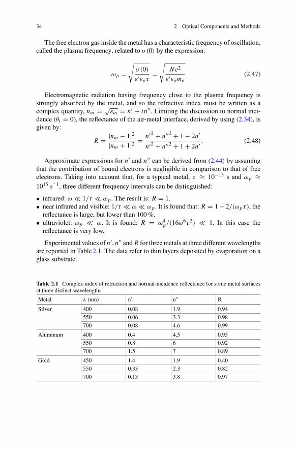
Approximate expressions for n′ and n′′ can be derived from (2.44) by assumingthat the contribution of bound electrons is negligible in comparison to that of freeelectrons. Taking into account that, for a typical metal, τ ≈ 10−13 s and ωp ≈1015 s
−1, three different frequency intervals can be distinguished:
• infrared: ω � 1/τ � ωp. The result is: R = 1.• near infrared and visible: 1/τ � ω � ωp. It is found that: R = 1− 2/(ωpτ), thereflectance is large, but lower than 100%.
• ultraviolet: ωp � ω. It is found: R = ω4p/(16ω
6τ 2) � 1. In this case thereflectance is very low.
Experimental values of n′, n′′ and R for threemetals at three different wavelengthsare reported in Table2.1. The data refer to thin layers deposited by evaporation on aglass substrate.
Table 2.1 Complex index of refraction and normal-incidence reflectance for some metal surfacesat three distinct wavelengths
Metal λ (nm) n′ n′′ R
Silver 400 0.08 1.9 0.94
550 0.06 3.3 0.98
700 0.08 4.6 0.99
Aluminum 400 0.4 4.5 0.93
550 0.8 6 0.92
700 1.5 7 0.89
Gold 450 1.4 1.9 0.40
550 0.33 2.3 0.82
700 0.13 3.8 0.97

2.2 Reflection and Refraction 35
One problemwith metallic mirrors is that the fraction of incident power that is notreflected is absorbed. When reflecting high-intensity beams, such as those comingfrom laser sources, the temperature rise due to this absorption may cause damage tothe metallic layer.
2.2.3 Anti-reflection Coating
The reflectance of a boundary separating two transparent media can be stronglymodified by inserting thin dielectric layers. The structure investigated in this section,shown in Fig. 2.4, consists of a single layer of refractive index n2 and thickness dseparating media 1 and 3 which have refractive indices n1 and n3, respectively. It isassumed that n1 < n2 < n3.
Considering a monochromatic plane wave perpendicularly incident on the bound-ary 1–2, and calling Ei the incoming electric field, thefirst contribution to the reflectedfield is: Er1 = ρ12Ei . The transmitted field Et1 = τ12Ei is partially back-reflectedby the interface 2–3, producing a second contribution to the reflected field givenby: Er2 = exp(iΔ)ρ23τ21Et1. This contribution is phase-shifted with respect to thefirst one because the wave has traveled back and forth inside layer 2. The shift is:Δ = 4πn2d/λ, where λ is the vacuumwavelength of the incident wave. Note that, inthis case, the coefficients ρ12 and ρ23 have the same sign, so that no contribution tothe phase shift between Er1 and Er2 is coming from the reflections at the interfaces.
Since the wave back-reflected from the surface 2–3 is partially reflected againwhen it reaches the surface 2–1, the total reflected field should be calculated byadding an infinite number of multiple reflections. Assuming that the reflectance ofthe interfaces 1–2 and 2–3 is small, which alsomeans that τ21τ12 ≈ 1, the summationcan be truncated by taking only the first two terms:
Er = Er1 + Er2 = [ρ12 + exp(iΔ)ρ23]Ei (2.49)
It is clear from (2.49) that Er vanishes through destructive interference if Er2and Er1 have the same amplitude, but opposite sign. The amplitudes of the two
Fig. 2.4 Anti-reflectioncoating
36 2 Optical Components and Methods
fields are the same if ρ12 = ρ23. According to (2.34), this is equivalent to sayingthat (n2/n1) = (n3/n2), or: n2 = √
n3n1. This means that the intermediate layershould have an index of refraction that is the geometric mean of n1 and n3. The twocontributions have opposite sign if Δ = π , which implies d = λ/(4n2). This meansthat the layer thickness must be a quarter of the wavelength inside the medium.
The fact that the condition imposed on the layer thickness d is wavelength-dependent indicates that there is a price to pay for eliminating reflection: the methodworks exactly at only one specific wavelength. In other words this anti-reflectioncoating is chromatic.
Instead of using the approximate expression given by (2.49), Er can be exactlycalculated by summing up an infinite number of multiple reflections or by writing theboundary conditions at the two interfaces. The latter approach is themore convenient,also because it can be more easily generalized to an arbitrary number of layers.
Consider first the interface 1–2; at left there are two waves, the incident wavewith field Ei and the reflected wave with field Er , at right there is a wave leaving theinterface, with field E ′
t and one arriving at the interface, with field E ′r . The boundary
conditions are:
Ei + Er = E ′t + E ′
r
Ei − Er = (n2/n1)(E ′t + E ′
r ). (2.50)
Taking into account that the wave crossing layer 2 acquires a phase shift of Δ/2,the following boundary conditions are written for the interface 2–3:
exp(iΔ/2)E ′t + exp(−iΔ/2)E ′
r = Et
exp(iΔ/2)E ′t + exp(−iΔ/2)E ′
r = (n3/n2)Et . (2.51)
Equations (2.50) and (2.51) constitute a linear system of four equations in fourvariables that can be exactly solved. The expression obtained for Er is:
Er = ρ12Ei + ρ23Eiτ12τ21exp(iΔ)
1 − ρ23ρ21exp(iΔ)(2.52)
Recalling that τ12τ21 = 1−ρ212, it is immediately apparent that the conditions for
a vanishing Er derived from (2.52) coincide with those imposed by the approximateexpression (2.49).
Table2.2 gives the index of refraction and the transparency window of severaldielectric materials. The index of refraction of the thin film depends not only onthe wavelength, but also on the preparation method, and so the values of n listedin Table2.2 should be only considered as indicative. The deposition of layers withprecisely controlled thickness is usually performed by vacuum evaporation methods.In order to have an idea of the required thickness, consider the anti-reflection coatingof an air-glass surface. Taking λ = 550 nm, n1 = 1 (air), and n3 = 1.52 (glass), the

2.2 Reflection and Refraction 37
Table 2.2 Properties of materials used for deposition of thin films
Material n Transparency window (µm)
Criolite Na3 Al F6 1.35 0.15–14
Magnesium fluoride MgF2 1.38 0.12–8
Silicon oxide Si O2 1.46 0.17–8
Aluminum oxide Al2O3 1.62 0.15–6
Silicon monoxide Si O 1.9 0.5–8
Zirconium oxide Zr O2 2.00 0.3–7
Cerium oxide CeO2 2.2 0.4–16
Titanium oxide T i O2 2.3 0.4–12
Zinc sulfide ZnS 2.32 0.4–14
Cadmium telluride CdT e 2.69 0.9–16
Silicon Si 3.5 1.1–10
Germanium Ge 4.05 1.5–16
Lead telluride PbT e 5.1 3.9–20
coating should be made with a material having n2 = √1.52 = 1.23 and thickness
d = 550/(4n2) = 112 nm. In practice, given the list of available materials inTable2.2, the best choice would be magnesium fluoride. A quarter-wave layer ofMgF2 reduces the reflectance from 4 to 1.3%.
By using more than one layer it is possible to cancel completely the reflectanceof the air-glass surface. For instance, the sequence of two quarter-wave layers withrefractive indices n2 and n′
2, produces a vanishing reflectance if n′2/n2 = √
n3/n1.Putting n1 = 1 e n3 = 1.52, one finds n′
2/n2 = 1.23. Zero-reflectance is obtainedby choosing from Table2.2 Zr O2 (n′
2 = 2.00) and Al2O3 (n2 = 1.62).Up to now normal incidence has been assumed. What happens if θi is different
from 0, as shown in Fig. 2.5? The phase difference between the first and the secondreflection becomes:
Fig. 2.5 Anti-reflectioncoating: non-normalincidence. The optical pathdifference between kr2 andkr1 is: 2n2 AB − n1 AH

38 2 Optical Components and Methods
Δ′ = 22πn2
λ
d
cosθt− 2πn1d
λtgθt sinθi = 4πn2d
λcosθt , (2.53)
where θt , the propagation angle inside medium 2, is related to θi by Snell’s law.It is important to note that, once d and n2 are fixed, the wavelength at which thereflectance vanishes, corresponding to Δ′ = π , depends on θi .
2.2.4 Multilayer Dielectric Mirror
By using a sequence of dielectric layers it is possible to obtain high reflectance atany desired wavelength. An important advantage of multilayer dielectric mirrors,as compared to metallic mirrors, is that there is no absorption. This means they canstand high intensities of visible lightwithout being damaged.An important differenceis that metallic mirrors have a broad-band reflectance, whereas the reflectance ofdielectric mirrors is narrow-banded.
The structure of a multilayer dielectric mirror is sketched in Fig. 2.6: betweenmedium 1 (air) and medium 2 (glass substrate) there is a sequence of alternatinglayers ABAB..A with refractive indices n A > nB , and n A > n2.
Clearly, the maximum reflectance will be obtained when the fields reflected by allthe interfaces add up in phase at the first interface, so that constructive interference isexploited. The field reflected at the interface 1-A is phase-shifted by π with respectto the incident field because n A > n1. The field reflected at the first A–B interfacedoes not suffer any phase-shift because n A > nB , but, upon arriving at the interface1-A, it will acquire the phase shift 4πn AdA/λ because of the propagation back andforth within the layer thickness dA. This second reflection will be in phase with thefirst one if the layer thickness corresponds to a quarter wavelength: dA = λ/(4n A).By analyzing all subsequent reflections in a similar way, it is immediately clear thatthe maximum reflectance, Rmax, is obtained if all the layers A and B have a quarterwavelength thickness. The number 2N + 1 of layers is always an odd number, inorder to ensure that the last reflection (occurring at the A-2 interface) is also in phasewith the previous ones.
Fig. 2.6 Multilayerdielectric mirror
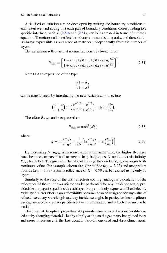
2.2 Reflection and Refraction 39
A detailed calculation can be developed by writing the boundary conditions ateach interface, and noting that each pair of boundary conditions corresponding to aspecific interface, such as (2.50) and (2.51), can be expressed in terms of a matrixequation. Therefore each interface introduces a transmission matrix, and the solutionis always expressible as a cascade of matrices, independently from the number oflayers.
The maximum reflectance at normal incidence is found to be:
Rmax =[1 − (n A/n1)(n A/n2)(n A/nB)2N
1 + (n A/n1)(n A/n2)(n A/nB)2N
]2. (2.54)
Note that an expression of the type
(1 − a
1 + a
),
can be transformed, by introducing the new variable b = ln a, into
(1 − a
1 + a
)=
(e−b/2 − eb/2
e−b/2 + eb/2
)= tanh
(b
2
).
Therefore Rmax can be expressed as:
Rmax = tanh2(Nξ), (2.55)
where:
ξ = ln(n A
nB
)+ 1
2N
[ln
(n A
n1
)+ ln
(n A
n2
)](2.56)
By increasing N , Rmax is increased and, at the same time, the high-reflectanceband becomes narrower and narrower. In principle, as N tends towards infinity,Rmax tends to 1. The greater is the ratio of n A/nB , the quicker Rmax converges to itsmaximum value. For example, alternating zinc sulfide (n A = 2.32) and magnesiumfluoride (nB = 1.38) layers, a reflectance of R = 0.99 can be reached using only 13layers.
Similarly to the case of the anti-reflection coating, analogous calculation of thereflectance of the multilayer mirror can be performed for any incidence angle, pro-vided the propagation path inside each layer is appropriately expressed. The dielectricmultilayer mirror offers a great flexibility because it can be designed for any value ofreflectance at any wavelength and any incidence angle. In particular, beam splittershaving any arbitrary power partition between transmitted and reflected beam can bemade.
The idea that the optical properties of a periodic structure can be considerably var-ied not by changing materials, but by simply acting on the geometry has gained moreand more importance in the last decade. Two-dimensional and three-dimensional

40 2 Optical Components and Methods
periodic structures made of dielectric or semiconductor materials, called photoniccrystals, are increasingly utilized in photonic devices. It is interesting to note that thiskind of phenomenon occurs also in Nature. For example, the brilliant colors of somebutterflies are due not to absorption, but to the presence of periodic dielectric layerson their wings. A phenomenon typical of periodic structures is iridescence, due to thefact that the wavelength of maximum reflectance depends on the incidence angle.This pleasing visual effect, also called opalescence, can be observed with opals,semi-precious stones consisting of a three-dimensional periodical arrangement ofsub-micrometric silica spheres.
2.2.5 Beam Splitter
As mentioned in the previous section, beam splitters are semi-reflecting mirrors thatdivide an optical beam into two parts propagating in different directions. In order tounderstand the behavior of some optical systems utilizing beam splitters, it is usefulto know the phase relation between transmitted and reflected fields.
Let τ = τoexp(iφτ ) and ρ = ρoexp(iφρ) be, respectively, the transmission andreflection coefficients for the electric field.The actual value takenby these coefficientsdepends onmany parameters, such as the beam-splitter structure, the incidence angle,and the wavelength of the incident beam. On the other hand, as will be shown, thephase difference φτ − φρ is expressed by a general law.
The scheme of Fig. 2.7 shows a beam-splitter symmetrically illuminated on bothsides by two identical light beams having the same phase, polarization, incidenceangle, and intensity Io. Calling I1 and I2 the intensities of the two output beams andassuming no losses, it should be expected, for symmetry reason, that I1 = I2 = Io.Since the field E1 at output 1 is the sum of two contributions, one coming fromreflection and the other from transmission, E1 = ρEo + τ Eo, the intensity at output1 is given by: I1 = |ρ + τ |2 Io. The condition I1 = Io is satisfied if:
|ρ + τ |2 = [ττ ∗ + ρρ∗ + 2Re(τρ∗)] = 1. (2.57)
Fig. 2.7 Two identical lightbeams impinging on the twosides of a beam splitter

2.2 Reflection and Refraction 41
Since ττ ∗ + ρρ∗ = 1, the quantity Re(τρ∗) = τoρocos(φτ − φρ) must be nil,therefore:
φτ − φρ = π
2. (2.58)
Equation (2.58) is a general relation, valid for any lossless beam-splitter, regardlessof the structure of the mirror or the incidence angle. The only limitation is that thebeam-splitter should be symmetrical. It is easy to generalize to the non-symmetricalcase: calling φτ and φρ the phase shifts for a beam incident to the left of the mirror,and φ′
τ and φ′ρ the phase shifts for a beam incident to the right of the mirror, instead
of (2.58), the following relation is found:
φτ + φ′τ − φρ − φ′
ρ = π. (2.59)
2.2.6 Total-Internal-Reflection Prism
The total-internal-reflection glass prism, shown in Fig. 2.8, behaves as a 100%-reflectance mirror if the incident beam undergoes total reflections at the two glass-airinterfaces. This happens if the incidence angles at the glass-air boundaries are largerthan the limit angle. In the case of the figure, θi = 45◦, which is larger than θc fora normal optical glass. The spurious reflection of about 4% at the air-glass inputinterface can be eliminated by an anti-reflection coating.
Whereas multilayer dielectric mirrors present high reflectance in a narrow wave-length band, the total-internal-reflection mirror is a broadband component. The onlylimitations could come from the decrease of the refractive index of the glass as thewavelength is increased, which could move θc to a value larger than 45◦.
An interesting property of the total-internal-reflection prism is that the reflectedbeam is always propagating in the opposite direction with respect to the incidentbeam, whatever is the angle of incidence, provided that the propagation vector of thebeam lies in a plane perpendicular to the prism axis (this is the plane of Fig. 2.8).Such a property is not shared by normal mirrors. Instead of a prism, it is possibleto use a trihedral (see Fig. 2.9), known as the corner cube. With this, the beam isretro-reflected after three internal reflections, and it is possible to obtain a back-propagating reflected beam for any direction of incidence. In practical applications,
Fig. 2.8 Total internalreflection prism

42 2 Optical Components and Methods
Fig. 2.9 Corner cube
Fig. 2.10 Cat’s eye
the back-reflectors placed on vehicles or on wayside posts have a structure imitatingan array of corner cubes.
This same property of the corner cube is also shared by the combination of a lensplus a mirror placed in the focal plane of the lens, known as a cat’s eye (see Fig. 2.10).
2.2.7 Evanescent Wave
A linearly polarized beam impinges on the glass-air planar boundary with an inci-dence angle θi ≥ θc. Assume that the boundary coincides with the x-y plane, that thepropagation vector k1 of the incident beam lies in the y-z plane, and that the beamis polarized along x as shown in Fig. 2.11a. Using the subscript 1 for glass and 2 forair, the electric fields of the incident and transmitted waves can be written as:
Ei = Eiexp[−i(ωt − k1y y − k1z z)]xEt = Etexp[−i(ωt − k2y y − k2z z)]x, (2.60)
where k1y = −kon1sinθi and k1z = kon1cosθi .The continuity condition at the boundary z = 0 imposes k1y = k2y . Using the
relation:
k2 = kon2 =√
k2y2 + k2z
2, (2.61)

2.2 Reflection and Refraction 43
Fig. 2.11 a Geometry fortotal internal reflection.b Transmission of theevanescent wave by a pair ofprisms
it is found: k2z = ko
√n2
2 − n12sin2θi . If θi > θc, the term under square root is
negative, so that k2z becomes imaginary. Putting√
n22 − n1
2sin2θi = iΓ n2, whereΓ is a real quantity, it is found:
Et = Etexp[−i(ωt + kon1sinθi y)]exp(−Γ kon2z)x. (2.62)
The condition of total internal reflection at the boundary between glass and airdoes not imply that there is no electromagnetic field in the air beyond the glass.Indeed Eq. (2.62) describes a wave, known as evanescent wave, running parallel tothe glass-air interface, with an amplitude that is an exponentially decreasing functionof the penetration distance z. The electromagnetic energy density inside medium 2,being proportional to |Et |2, is also exponentially decreasingwith z, becoming smallerby a factor e−1 at the distance:
δ = 1
2Γ kon2= λ
4π√
n12 sin2 θi − n2
2. (2.63)
For instance, if n1 = 1.5, n2 = 1, θi = π/4, it follows that Γ = 0.354, thereforeδ = λ/4.44. Taking the central wavelength of the visible range, λ = 0.55 µm, it isfound that δ = 120 nm.
In order to derive the amplitude of the transmitted and reflected fields, the follow-ing boundary conditions are written:
Ei + Er = Et (2.64)
Ei − Er = iγ Et , (2.65)
where γ = Γ n2/(n1cosθi ) is a real quantity. The solutions of (2.64) and (2.65) are:
Et = 2
1 + iγEi ; Er = 1 − iγ
1 + iγEi . (2.66)

44 2 Optical Components and Methods
Note that |Ei | = |Er |, thus confirming total reflectance, even if |Et | is differentfrom 0.
By placing a second prism in the vicinity of the totally reflecting one, it is possibleto exploit a tunnel effect, by “catching” some part of the evanescent wave. Such atechnique, called frustrated total internal reflection, allows for the realization of apartially transmitting mirror, with a transmittance controlled by the thickness ofthe air-gap between the two prisms. Consider the configuration in Fig. 2.11b, wherethere is an air-gap of thickness d between the two prisms. In order to write down theboundary conditions at the two interfaces, it is necessary to assume that inside thegap there are two evanescent waves decaying in opposite directions. The continuityconditions at the first interface are:
Ei + Er = E ′t + E ′
r , (2.67)
andEi − Er = iγ (E ′
t − E ′r ), (2.68)
where E ′t and E ′
r are the fields of the two evanescent waves, the first decaying asa function of z and the second growing as a function of z. Similarly, the continuityconditions at the second interface are:
exp[−d/(2δ)]E ′t + exp[d/(2δ)]E ′
r = Et , (2.69)
andexp[−d/(2δ)]E ′
t − exp[d/(2δ)]E ′r = −(i/γ )Et . (2.70)
By eliminating E ′t and E ′
r , Et and Er can be calculated. In particular, the trans-mittance T is found to be:
T = |Et |2|Ei |2 = exp(−d/δ)
[(1 + exp(−d/δ)
)/2
]2+ A
(1 − exp(−d/δ)
)2 , (2.71)
where A = (1− γ 2)2/(16γ 2). It is seen from (2.71) that, for d tending to 0, T tendsto 1, as expected. If d δ, T is approximated by:
T ≈ 4exp(−d/δ)
1 + 4A, (2.72)
which shows an exponential decay of T as a function of d. The set of two prisms istherefore equivalent to a variable-transmittance attenuator.

2.2 Reflection and Refraction 45
2.2.8 Thin Lens and Spherical Mirror
So far in this chapter only situations involving planewaves and plane boundaries havebeen considered. In this section spherical boundaries are discussed, concentratingthe attention on the important optical component of the lens.
The lens, as shown in Fig. 2.12, is formed by joining two spherical caps madeof glass. The radii of curvature of the two surfaces, ρ1 and ρ2, are conventionallytaken to be positive if the surfaces are convex. The thin-lens approximation consistsin assuming that the lens thickness is much smaller than the radii of curvature of thetwo spherical surfaces. Neglecting reflections at the two surfaces, the effect of thelens on the incident field E1 is described by a transmission function τ f (x, y):
E2(x, y, z, t) = τ f (x, y)E1(x, y, z, t). (2.73)
This transmission function has a unitary modulus and a phase that is locallydependent on the glass thickness:
τ f (x, y) = exp{iko[nΔ(x, y) + Δo − Δ(x, y)]}, (2.74)
where n is the glass refractive index, Δ(x, y) is the lens thickness at the transversalposition (x, y), and Δo = Δ(0, 0) is the thickness on the optical axis.
The phase shift is the sum of two contributions, one due to the path inside theglass, konΔ(x, y), and the other due to the path in air, ko[Δo − Δ(x, y)]. The lensthickness at the generic point (x, y) is:
Δ(x, y) = Δo +√
ρ12 − (x2 + y2) − ρ1 +√
ρ22 − (x2 + y2) − ρ2 (2.75)
Fig. 2.12 Thin lens made of two glass caps with radii of curvature ρ1 and ρ2

46 2 Optical Components and Methods
Equation (2.75) can be simplified by assuming that the lens diameter is muchsmaller than the radii of curvature of the two surfaces, so that:
√ρ12 − (x2 + y2) = ρ1
√
1 − x2 + y2
ρ12≈ ρ1
[1 − x2 + y2
2ρ12
], (2.76)
and √ρ22 − (x2 + y2) ≈ ρ2
[1 − x2 + y2
2ρ22
]. (2.77)
In the power expansion of the square-root terms, only the first-order terms in(x2 + y2) are kept. This is equivalent to approximate the spherical surface witha paraboloidal surface, similarly to the paraxial approach used in Chap. 1 for thedescription of spherical waves.
Inserting (2.76) and (2.77) into (2.75):
Δ(x, y) = Δo − x2 + y2
2
(1
ρ1+ 1
ρ2
). (2.78)
By substituting inside (2.74):
τ f (x, y) = exp(ikonΔo)exp
[−iko
x2 + y2
2 f
], (2.79)
where f , called focal length, is defined by the relation:
1
f= (n − 1)
(1
ρ1+ 1
ρ2
)(2.80)
Note that f has a sign: f > 0 means converging lens, f < 0 diverging lens. Sincef depends on n, and, in turn, n changes with wavelength, the lens focuses differentwavelengths to different distances, that is, it suffers from a chromatic aberration.
The spherical mirror is described similarly to the lens, the main difference beingthat it works in reflection instead of transmission. The mirror shown in Fig. 2.13has center in O and radius of curvature ρ. Consider a beam parallel to the opticalaxis, incident at point P with an incidence angle α. The reflected beam intersects theoptical axis at point F. The distance of F from O is: O F = O P/(2cosα). Since O Fdepends on α, parallel beams impinging on the mirror in different points producereflected beams crossing the optical axis at different positions. However, if onlybeams traveling close to the optical axis are considered (i.e. where cosα ≈ 1), itis found that O F ≈ O P/2 = ρ/2. Under this approximation, which is equivalentto treating the surface as paraboloidal instead of spherical, it can be said that thespherical mirror brings all parallel beams to converge at a single point a distance ρ/2from the mirror surface. In other words, the mirror behaves in reflection just as a lens

2.2 Reflection and Refraction 47
Fig. 2.13 Spherical mirrorwith radius of curvature ρ
having a focal length f = ρ/2. Note that the focal length of the spherical mirroris independent of the wavelength. All large astronomical telescopes use parabolicmirrors instead of lenses.
2.2.9 Focusing Spherical Waves
A spherical wave traveling along the z axis impinges on a thin lens located at theplane z = 0. If R1 is the radius of curvature of the wavefront, then, under the paraxialapproximation, the electric field E1 of the wave at z = 0 is given by:
E1(x, y, 0) = Ao
R1exp
(iko
x2 + y2
2R1
). (2.81)
The field distribution transmitted through the lens, E2 = τ f E1, calculated byusing (2.79) and (2.81), is again that of a spherical wave, with the modified radiusof curvature R2, which is related to R1 by:
1
R2= 1
R1− 1
f. (2.82)
If R1 = f , R2 becomes infinite, which means that a spherical wave originatingfrom the left focus is converted into a parallel beam (planewave). If R1 > f , R2 < 0,indicating that the diverging wave is converted into a converging wave. If R1 f ,R2 ≈ f , that is, a plane wave is converted into a spherical wave converging at theright focal plane. In practice, the wave will not converge to a point, but the beamspot at focus will be described by an Airy function (see Sect. 1.6.1) because of thediffraction effect introduced by the finite dimension of the lens-diameter.
The ratio between the lens radius and the focal length is called numerical aperture(NA) of the lens. It describes the light-gathering capacity of the lens.

48 2 Optical Components and Methods
Relation (2.82) can also be interpreted in the following way: given a point-likeobject P at distance R1 on the left, the lens creates a real image Q of P at distanceR2 on the right. This is the standard interpretation given by geometrical optics. IfP is on the optical axis, Q is also on the same axis. What happens if the point-likeobject P′ is off-axis? Assigning to P′ the coordinates (xo, 0, R1), the electric field ofthe spherical wave originated at P′, evaluated at the lens plane z = 0, is now:
E1(x, y, 0) = Ao
R1exp
{ iko
2R1[(x − xo)
2 + y2]}. (2.83)
Using again the relation E2 = τ f E1, after some algebra the following expressionis found for E2:
E2(x, y, 0) = Aoexp(iφ)
R1exp
{iko
2R2
[(x + f
R1 − fxo)
2 + y2]}
, (2.84)
whereφ depends on xo and on the lens parameters, but not on x and y. Equation (2.84)shows that the image of P′ is at point Q′ having coordinates [− f xo/(R1− f ), 0, R2].It can be said that the lens creates an imageQQ′ of the segment PP′. If R1 > f , the realimage is upside-down, with a magnification f/(R1 − f ). This approach is thereforeequivalent to the geometrical-optics treatment. The topic of image formation hasimportant applications but will not be further discussed in this text.
Another case to be considered is that of a plane wave having a propagation direc-tion slightly tilted with respect to the optical axis. To simplify the discussion it isassumed that the wave vector k is in the plane x-z, forming an angle α with x . Atz = 0 the incident field is expressed as E1 = Aoexp(ikoαx), where sin α has beenapproximated as α. After using E2 = τ f E1 again, and applying some algebra, it isfound that:
E2(x, y, 0) = Aoexp(iφ)exp
{− iko
2 f
[(x − α f )2 + y2
]}(2.85)
where φ = kα2 f/2. Equation (2.85) describes a spherical wave that converges atthe point (α f, 0, f ) located on the right focal plane, as shown in Fig. 2.14.
Generalizing the treatment, it can be stated that a biunique correspondence isestablished between the propagation direction of the incident wave and points on theright focal plane.
2.2.10 Focusing Gaussian Spherical Waves
If the wave impinging on the lens is a Gaussian spherical wave with a complex radiusof curvature of the wavefront q1, then it can be immediately shown, by using (2.73)and (2.79), that the transmitted wave is still a Gaussian spherical wave. The new

2.2 Reflection and Refraction 49
Fig. 2.14 A plane wavecorresponds to a point at thefocal plane of a lens
complex radius of curvature q2 satisfies the relation:
1
q2= 1
q1− 1
f. (2.86)
Since the beam radius is unchanged by crossing the lens, w1 = w2, one finds that(2.86) coincides with (2.82). As an example, if f > 0 and E1 describes a divergingGaussian wave with R1 > f , the transmitted Gaussian wave has a negative radiusof curvature of the wavefront, R2 < 0, and is, therefore, converging. There is a basicdifference between this case and the one treated in the previous section: the theoryof Gaussian waves accounts intrinsically for diffraction effects, such that the waveconverges to a finite-size beam spot.
Once q2 at z = 0 is assigned, it is possible to obtain the distance z f at which thefocused beam takes the minimum radius, and also the minimum radius w f , by usingrelations 1.35 and 1.36. The results of the calculation are:
z f = |R2|1 + [λ|R2|/(πw2
1)]2, w f = w1√
1 + [πw21/(λ|R2|)]2
. (2.87)
Assuming that R1 f , which means |R2| ≈ f , and πw21 λ f , the relations of
(2.87) simplify as follows:
z f ≈ f, w f ≈ λ f
πw1(2.88)
It is useful to calculate the Rayleigh length at focus:
z f R = πw2f
λ≈ λ
π
(f
w1
)2
. (2.89)
50 2 Optical Components and Methods
The length 2z f R defines the field depth, that is, the interval of distance over whichthe beam remains focused. As an example, putting f = 20 cm, w1 = 2 mm, λ =0.5µm (note thatπw2
1/(λ f ) is 1), one finds thatw f = 16µm and z f R = 1.6mm.From a mathematical point of view, the Gaussian spherical wave has an infinite
extension on the transversal plane. In reality, practical optical components have alimited size, and so the tails of the Gaussian distribution are lost. The empiricalcriterion for applying the theory of Gaussian waves is if the lost power is sufficientlysmall. Considering a lens (or amirror)with diameter d, the power fraction interceptedby the lens is given by:
T f =∫ d/20 2πr exp(− 2r2
w2 )dr∫ ∞0 2πr exp(− 2r2
w2 )dr= 1 − exp
(− d2
2w2
)(2.90)
As an example, if d = 2w, the intercepted power fraction is 86%, if d = 3w,T f = 0.99. Therefore, if d > 3w, it is reasonable to assume the applicability of theGaussian wave theory.
2.2.11 Matrix Optics
Within the geometrical optics approximation, a useful approach is that of associatinga 2 × 2 matrix, called ABC D matrix, with each optical component.
The ray present at the coordinate z is characterized by two parameters, the distancer(z) from the optical axis, and the angle its direction formswith the optical axis,φ(z).Within the paraxial approximation, φ(z) is simply the derivative of r with respect toz. The ray is represented by a one-column matrix:
R =(
rφ
). (2.91)
Every optical component is represented by a 2 × 2 matrix of the type:
M =(
A BC D
), (2.92)
connecting the output vector Ru to the input vector Ri according to:
Ru = MRi. (2.93)
Using refraction laws and the properties of lenses and mirrors discussed in thepreceding sections, the ABC D matrices of the components shown in Fig. 2.15 canbe written as follows.
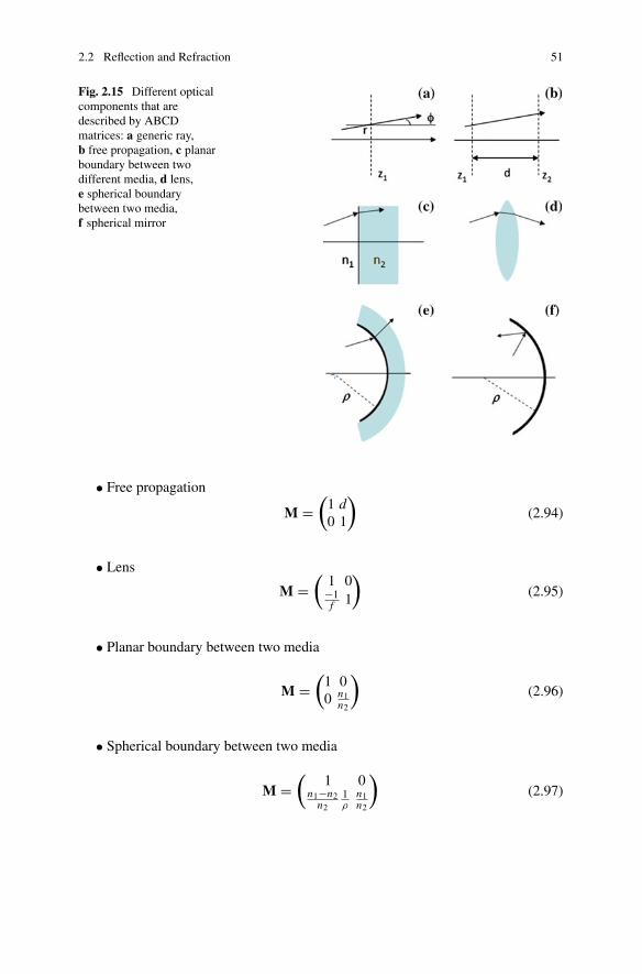
2.2 Reflection and Refraction 51
Fig. 2.15 Different opticalcomponents that aredescribed by ABCDmatrices: a generic ray,b free propagation, c planarboundary between twodifferent media, d lens,e spherical boundarybetween two media,f spherical mirror
• Free propagation
M =(1 d0 1
)(2.94)
• Lens
M =(
1 0−1
f 1
)(2.95)
• Planar boundary between two media
M =(1 00 n1
n2
)(2.96)
• Spherical boundary between two media
M =(
1 0n1−n2
n21ρ
n1n2
)(2.97)

52 2 Optical Components and Methods
• Spherical mirror
M =(
1 0−2ρ
1
)(2.98)
Note that the determinant of a generic ABC D matrix is given by:
AD − BC = n1/n2. (2.99)
If the two media are the same, the determinant is equal to 1, as expected if theoptical element does not introduce losses.
Anoptical systemmadeby a cascadeof various elements is represented by amatrixthat is the ordered product of all the individual matrices describing each element.The order is important because the matrix product is generally non-commutative.
2.3 Fourier Optics
As discussed in Sect. 1.6, the Fraunhofer approximation of the diffraction integral isonly valid in the far field, at distances from the screen that are much larger than thetypical size of optical instruments. Therefore, it is of great practical importance tofind a method of transporting the far-field behavior to short distances. In this sectionit will be shown that the insertion of a lens can solve the problem.
Consider a thin lens having a focal distance f and positioned at z = 0, that isilluminated from the left by a wave propagating along the z axis. By assuming thatthe field distribution in the left focal plane of the lens is known, Ei (xo, yo,− f ),the aim of the calculation is to derive the field distribution at the right focal plane,E f (x f , y f , f ). The calculation is performed according to the following scheme:(a) the wave is propagated from the plane z = − f to the plane z = 0 by usingFresnel diffraction, as expressed by (1.50); (b) at z = 0 the field distribution is mul-tiplied by the lens transmission function τ f (x, y); (c) the obtained field distributionis propagated to the plane z = f by using again Fresnel diffraction.
Step (a) of the calculation gives:
E(x, y, 0) = i exp(ik f )
λ f
∫ ∞
−∞dxo
∫ ∞
−∞Ei (xo, yo,− f )exp
{ik
2 f[(x − xo)
2 + (y − yo)2]
}dyo. (2.100)
Steps (b) and (c) require calculating the integral:
E f (x f , y f , f ) = i exp(ik f )
λ f
∫ ∞
−∞dx
∫ ∞
−∞E(x, y, 0)τ f (x, y)exp
{ ik
2 f[(x − x f )
2 + (y − y f )2]
}dy. (2.101)

2.3 Fourier Optics 53
By inserting (2.100), and the expression of τ f given by (2.79), into (2.101), oneobtains:
E f (x f , y f , f ) = − exp[2ik f + ik(n − 1)Δo]λ2 f 2
∫ ∞
−∞dxo
∫ ∞
−∞dyo Ei (xo, yo,− f )
∫ ∞
−∞dx
∫ ∞
−∞dy exp
{ik
2 f[(x − x f )
2 + (y − y f )2 + (x − xo)
2 + (y − yo)2 − x2 − y2]
}. (2.102)
The dxdy integral is solved bywriting the integrand function as the exponential ofa square term. Noting that: (x −x f )
2+(y− y f )2+(x −xo)
2+(y− yo)2−x2− y2 =
(x − xo − x f )2 + (y − yo − y f )
2 − 2(xox f + yo y f ), it is finally found:
E f (x f , y f , f ) = exp[2ik f + ik(n − 1)Δo]λ f
∫ ∞
−∞dxo
∫ ∞
−∞dyo Ei (xo, yo,− f )exp
[ik
f(xox f + yo y f )
]. (2.103)
Equation (2.103) represents a very important result: it states that the field dis-tribution at the right-hand focal plane of the lens is the two-dimensional Fouriertransform of the distribution at the left-hand plane. Such a result is consistent withthe consideration, developed at the end of Sect. 2.2.9, that a biunique correspondenceexists between the propagation direction of the incident wave and points on the rightfocal plane. In fact to perform the spatial Fourier transform of the field distributionis the same as describing the field by a superposition of plane waves.
Equation (2.103) has a fundamental role in many optical processing techniques.For instance, it suggests that spatial filtering of optical signals can be performedby placing an appropriate filter at the right-hand focal plane, and reconstructingthe filtered signal with a second confocal lens. An example is shown in Fig. 2.16,where a pinhole is used as a low-pass filter, i.e. a filter transmitting only low spatialfrequencies.
Fig. 2.16 Scheme of spatial filtering of an optical beam

54 2 Optical Components and Methods
2.4 Spectral Analysis
The electric field E(t) associated with a generic light beam can always be described,as discussed in Sect. 2.1, as a weighted superposition of sinusoidal functions oscil-lating at different frequencies. The Fourier transform of E(t) is the complex quantityE(ω) (given by (2.10)) that represents the amplitude and the phase of the field com-ponent at angular frequency ω.
The power spectrum of the light beam, S(ω), is defined as:
S(ω) = cεo|E(ω)|2
2(2.104)
It should benoted that S(ω)does not contain any informationon the phase of E(ω).This means that the knowledge of S(ω) is not sufficient, in general, for reconstructingthe temporal behavior of E(t).
The usual method to measure the power spectrum of an optical signal is that ofcollimating a sample beam and sending it through a dispersive system in order toangularly separate the different frequency components. This method was introducedby Newton, who first observed the spectrum of solar light through a glass prism.Instead of using the dispersion properties of glass, angular separation can be gen-erated by diffraction gratings, i.e. structures with periodic transmission functions.Almost all modern commercial spectrometers are based on gratings. As will be seen,there is another method, consisting of the use of a narrow-band tunable filter. Thismethod is conceptually similar to that used to measure the power spectrum of electri-cal signals. In the optical case, the narrow-band filter is a Fabry-Perot interferometer.
An important parameter for assessing the performance of a spectrometer is thefrequency resolution δν, defined as the minimum frequency separation that can beresolved by the spectrometer. Calling νo the central frequency of the signal to beanalyzed, the resolving power of the instrument at that frequency is calculated as:
Pr = νo
δν= λo
δλ, (2.105)
where λo = c/νo and δλ is the minimumwavelength separation that can be resolved.When writing the right-hand member of (2.105), the assumption δν � νo has beenmade. In fact, by differentiating νλ = c around νo, it is obtained: λodν − νodλ = 0,hence (2.105).
2.4.1 Dispersive Prism
Optical components fabricated from dispersive materials refract light of differentwavelengths by different angles. Consider a collimated light beam that impingeson a glass prism at an incidence angle θi , as shown in Fig. 2.17. Since the angle

2.4 Spectral Analysis 55
Fig. 2.17 Dispersive prism
of refraction depends on the refractive index, which is wavelength dependent, thedirection of the emergent beam is also wavelength dependent.
The deflection angle θ , calculated from the refraction law, is given by:
θ = θi − α + arcsin[sin α
√n2 − sin2θi − sinθicosα
], (2.106)
where α is the prism angle and n the refractive index of the glass.What’s the minimumwavelength separation δλ that can be resolved? Clearly, this
depends on the minimum angular resolution. Even assuming that the incident beamis monochromatic and perfectly collimated, the output beam will present an angularspread due to diffraction. If L is the minimum size between prism size and incidentbeam diameter, and λo is the wavelength of the incident beam, the angular spreadwill be δθ ≈ λo/L . In order to resolve two different wavelengths, the difference intheir deflection angles should be larger than δθ . Therefore, the wavelength resolutionis given by:
δλ =(
dθ
dλ
)−1
δθ, (2.107)
where dθ/dλ is calculated by assigning the dependence of n on λ. Taking typicalvalues for the parameters appearing inside (2.106), α = θi = π/4, n = 1.5, it isfound that dθ/dλ ≈ dn/dλ. Therefore, the resolving power of the dispersive prismcan be written as:
Pr = λo
δλ≈ L
dn
dλ(2.108)
If dn/dλ = (10 µm)−1, and L = 1 cm, then Pr = 103.
2.4.2 Transmission Grating
The diffraction grating is an optical component that periodically modulates (in thetransversal direction) the amplitude or phase of an incident wave. The treatmenthere is limited to linear gratings in which the diffracting elements consist of parallellines ruled on glass or metal. These gratings may be used either in transmission or

56 2 Optical Components and Methods
in reflection. The most common transmission grating is made of a periodic array ofnarrow slits on an opaque screen. The slit width is smaller than the wavelength, sothat the diffracted field has a wide angular spread.
Assume that the grating plane coincides with the x-y plane, and that the slits areparallel to the x axis and have spacing d. The wave vector of the incident plane wavelies in the y-z plane and forms an angle θi with the z axis, as shown in Fig. 2.18. Thespatial distribution of the field in the half-space beyond the grating is determined bythe interference among the diffracted waves coming from all the slits. Note that inthe approximation of a far-field projection the interfering beams can be consideredas parallel. Diffractive interference will occur only in those directions satisfying thecondition:
qλ = d(sin θq − sin θi ), (2.109)
where q = 0,±1,±2, . . .. Equation (2.109) defines a discrete set of directions inwhich a diffracted beam can be observed.
In particular, the beam corresponding to the order of q = 0 is simply the trans-mitted beam: sin θ0 = sin θi .
Equation (2.109) says that the directions of the diffraction orders (except for theorder 0) are wavelength-dependent. Therefore the grating is a dispersive structure.As such it can be used, like the dispersive prism, to analyze the power spectrum ofan optical signal.
Similarly to the case of the prism, the limit to the wavelength resolution comesfrom the diffraction effect due to the finite size of the grating. At θi = 0 the first-orderdiffracted field, as derived from the theory of Fraunhofer diffraction, is expressed by(1.69). This equation shows that, in the far-field plane at distance z from the gratingplane, the peak corresponding to the diffracted field is transversally displaced by
Fig. 2.18 Transmissiongrating. The path differencebetween the two diffractedbeams is: AC − B H =d sin θq − d sin θi

2.4 Spectral Analysis 57
λz/d and has a width λz/L . This means that the resolving power of the grating is:
Pr = λz/d
λz/L= L
d= N , (2.110)
where L is the size of the grating, and N the number of illuminated slits. Note that Ncoincides with L/d only if the collimated beam fully covers the grating surface. Byintroducing the number of slits per unit length, fo = 1/d, N = fo L . Taking, e.g.,fo = 103 mm−1 and L = 1 cm, the resolving power is 104, one order of magnitudelarger than that of the dispersive prism. As shown by (2.109), the angular separationbetween two wavelengths grows by increasing the diffraction order: for the order q,the resolving power becomes Pr = q N . However, the fraction of diffracted opticalpower in a given order decreases with the value of q.
A problem arising from the use of a grating in spectral analysis is an ambiguitythat can appear if the optical signal has a very broad wavelength spectrum. Indeed,considering (2.109), it can be seen that the first-order diffraction of the wavelengthλ1 appears in the same direction as the second-order diffraction of the wavelengthλ1/2. This means that there is an upper limit to the spectral width that can be unam-biguously analyzed by the grating. For very broad spectra it is more convenient touse a dispersing prism.
Instead of an amplitude grating, a phase grating can be used: this is discussed inSect. 1.6.2. Most of the properties of the amplitude grating are also shared by thephase grating.
The description of the diffraction properties of gratings assumes that the diffractedfield is observed in the far field. Since, in order to have a good resolving power,the grating size must be of the order of centimeters, far field means a distance ofkilometers, as discussed in Sect. 1.6. However, by exploiting the properties of lenses(or spherical mirrors) discussed in Sect. 2.3, the far field can be brought to the focalplane of a lens placed beyond the grating: this is the approach adopted by all practicalspectrometers.
2.4.3 Reflection Grating
Reflection gratings are made by creating a linear alternation of reflecting and opaquezones on a surface, as shown in Fig. 2.19.
In the case of the reflection grating, the diffractive effects are observed in thebackward direction. The directions of constructive interference are given by:
qλ = d(sin θi + sin θq), (2.111)
where q is 0,±1,±2, . . . and θi is the incidence angle. Inside (2.111) diffractionangles are positive if the corresponding directions stay in the upper half-plane with

58 2 Optical Components and Methods
Fig. 2.19 Reflectiongrating. The black zones areopaque, and the grey zonesare reflecting
respect to the grating plane normal. The zeroth-order beam propagates at the angleθ0 = −θi , corresponding to specular reflection, that is independent from λ.
In a transmission grating the diffraction lobe due to a single slit presentsmaximumintensity in correspondence with the direction of incidence. As a consequence, thelargest fraction of diffracted power goes to order 0. This is useless from the pointof view of spectral analysis because the zeroth order is not dispersive. Similarly, inthe case of a reflection grating the largest fraction of diffracted power would appearin specular reflection. Diffraction gratings can be optimized such that most of thepower goes into a certain diffraction order, q0 �= 0, leading to a high diffractionefficiency for that order. This is indeed possible by using a so-called blazed grating(see Fig. 2.20), in which the reflecting elements are tilted by an angle θg with respectto the grating plane, obtaining a sawtooth-like profile.
The specular reflection from the tilted elements appears in a direction formingan angle θr = −(θi − θg) + θg = (2θg − θi ) with the normal to the grating plane.It is intuitive to expect that the maximum of the diffraction lobe associated to asingle reflecting element occurs in the direction of specular reflection relative to thatsegment. By imposing that such direction coincides with that of the diffraction orderq0, θqo = θr , the following relation is found:
θg = θi + θqo
2. (2.112)
By substituting (2.112) inside (2.111):
qoλ = d[sin θi + sin (2θg − θi )]. (2.113)
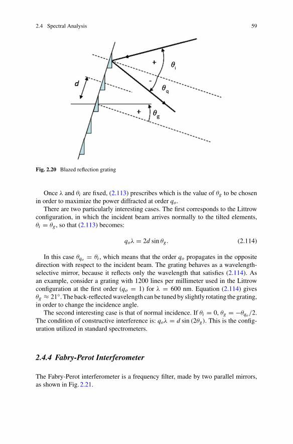
2.4 Spectral Analysis 59
Fig. 2.20 Blazed reflection grating
Once λ and θi are fixed, (2.113) prescribes which is the value of θg to be chosenin order to maximize the power diffracted at order qo.
There are two particularly interesting cases. The first corresponds to the Littrowconfiguration, in which the incident beam arrives normally to the tilted elements,θi = θg , so that (2.113) becomes:
qoλ = 2d sin θg. (2.114)
In this case θqo = θi , which means that the order qo propagates in the oppositedirection with respect to the incident beam. The grating behaves as a wavelength-selective mirror, because it reflects only the wavelength that satisfies (2.114). Asan example, consider a grating with 1200 lines per millimeter used in the Littrowconfiguration at the first order (qo = 1) for λ = 600 nm. Equation (2.114) givesθg ≈ 21◦. The back-reflectedwavelength canbe tunedby slightly rotating the grating,in order to change the incidence angle.
The second interesting case is that of normal incidence. If θi = 0, θg = −θqo/2.The condition of constructive interference is: qoλ = d sin (2θg). This is the config-uration utilized in standard spectrometers.
2.4.4 Fabry-Perot Interferometer
The Fabry-Perot interferometer is a frequency filter, made by two parallel mirrors,as shown in Fig. 2.21.
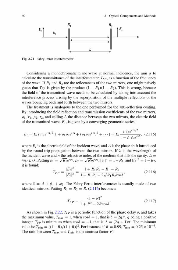
60 2 Optical Components and Methods
Fig. 2.21 Fabry-Perot interferometer
Considering a monochromatic plane wave at normal incidence, the aim is tocalculate the transmittance of the interferometer, TFP, as a function of the frequencyof the wave. If R1 and R2 are the reflectances of the two mirrors, one might naivelyguess that TFP is given by the product (1 − R1)(1 − R2). This is wrong, becausethe field of the transmitted wave needs to be calculated by taking into account theinterference process arising by the superposition of the multiple reflections of thewaves bouncing back and forth between the two mirrors.
The treatment is analogous to the one performed for the anti-reflection coating.By introducing the field reflection and transmission coefficients of the two mirrors,ρ1, τ1, ρ2, τ2, and calling L the distance between the two mirrors, the electric fieldof the transmitted wave, Et , is given by a converging geometric series:
Et = Eiτ1τ2eiΔ/2[1 + ρ1ρ2eiΔ + (ρ1ρ2eiΔ)2 + · · · ] = Eiτ1τ2eiΔ/2
1 − ρ1ρ2eiΔ, (2.115)
where Ei is the electric field of the incident wave, andΔ is the phase shift introducedby the round-trip propagation between the two mirrors. If λ is the wavelength ofthe incident wave and n the refractive index of the medium that fills the cavity, Δ =4πnL/λ. Putting ρ1 = √
R1eiφ1 , ρ2 = √R2eiφ2 , |τ1|2 = 1− R1, and |τ2|2 = 1− R2,
it is found:
TF P = |Et |2|Ei |2 = 1 + R1R2 − R1 − R2
1 + R1R2 − 2√
R1R2cosδ, (2.116)
where δ = Δ + φ1 + φ2. The Fabry-Perot interferometer is usually made of twoidentical mirrors. Putting R1 = R2 = R, (2.116) becomes:
TF P = (1 − R)2
1 + R2 − 2Rcosδ. (2.117)
As shown in Fig. 2.22, TFP is a periodic function of the phase delay δ, and takesthe maximum value, Tmax = 1, when cosδ = 1, that is δ = 2qπ , q being a positiveinteger. TFP is minimum when cosδ = −1, that is, δ = (2q + 1)π . The minimumvalue is: Tmin = [(1− R)/(1+ R)]2. For instance, if R = 0.99, Tmin = 0.25×10⁻⁴.The ratio between Tmax and Tmin is the contrast factor F :
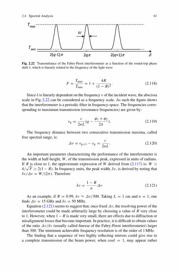
2.4 Spectral Analysis 61
Fig. 2.22 Transmittance of the Fabry-Perot interferometer as a function of the round-trip phaseshift δ, which is linearly related to the frequency of the light wave
F = Tmax
Tmin= 1 + 4R
(1 − R)2. (2.118)
Since δ is linearly dependent on the frequency ν of the incident wave, the abscissascale in Fig. 2.22 can be considered as a frequency scale. As such the figure showsthat the interferometer is a periodic filter in frequency-space. The frequencies corre-sponding to maximum transmission (resonance frequencies) are given by:
νq = c
2nL(q − φ1 + φ2
2π). (2.119)
The frequency distance between two consecutive transmission maxima, calledfree spectral range, is:
Δν = νq+1 − νq = c
2nL. (2.120)
An important parameter characterizing the performance of the interferometer isthe width at half-height, W , of the transmission peak, expressed in units of radians.If R is close to 1, the approximate expression of W derived from (2.117) is: W �4/
√F � 2(1− R). In frequency units, the peak width, δν, is derived by noting that
δν/Δν = W/(2π). Therefore:
δν = 1 − R
πΔν (2.121)
As an example, if R = 0.99, δν ≈ Δν/300. Taking L = 1 cm and n = 1, onefinds Δν = 15 GHz and δν = 50 MHz.
Equation (2.121) seems to suggest that, once fixedΔν, the resolving power of theinterferometer could be made arbitrarily large by choosing a value of R very closeto 1. However, when 1− R is made very small, there are effects due to diffraction ormisalignment losses that become important. In practice, it is difficult to obtain valuesof the ratio Δν/δν (usually called finesse of the Fabry-Perot interferometer) largerthan 300. The minimum achievable frequency resolution is of the order of 1MHz.
The finding that a sequence of two highly reflecting mirrors could give rise toa complete transmission of the beam power, when cosδ = 1, may appear rather

62 2 Optical Components and Methods
counter-intuitive. It is important to take into account that TFP is the result of asteady-state calculation. If it is assumed that the interferometer is illuminated byan intensity step-function, starting at t = 0, it is clear that the initial transmittanceis very low. If the incident frequency corresponds to a resonance, what happens isthat optical power is progressively accumulated inside the interferometer, and theoutput intensity progressively grows, by approaching asymptotically the value of theinput intensity. As an example, if R = 0.99 and the incident power is 1W, the outputpower of 1Wwill be reached onlywhen the power bouncing back and forth inside thecavity attains the value of 100W. It can be shown that the time constant controllingsuch a transient is the reciprocal of the frequency resolution δν. In other terms, thelarger is the resolving power of the instrument, the longer is its time-response.
In order to use the Fabry-Perot interferometer for spectral analysis, one should beable to continuously shift the transmission peaks by changing the optical path nL , sothat a scan of the frequency interval between two consecutive resonant frequenciescan be performed. What is the change in L , δL , required to scan a given free spectralrange? Assuming that the interferometer is initially tuned to νq , the condition tosatisfy is that the new resonance ν′
q−1 corresponding to the modified length L + δLshould coincide with νq :
νq = qc
2L= ν′
q−1 = (q − 1)c
2(L − δL)(2.122)
From (2.122) it is found:
δL = L
q= c
2νq= λq
2. (2.123)
Therefore in order to scan a free spectral range it is sufficient to change the mirrordistance by half wavelength.
In practical cases, the scan is performed by attaching one of the mirrors to apiezoceramic, and varying the ceramic thickness by the application of a slow voltageramp. The mirror displacement is proportional to the applied voltage, and thereforechanges linearly with time. In such a measurement, the time scale is transformedinto a frequency scale, and so the observed temporal dependence of the transmittedpower coincides with the spectral distribution of the incoming optical signal.
As an alternative approach, scanning of the resonant frequency can also be per-formed by keeping L fixed and changing the refractive index of the medium insidethe Fabry-Perot cavity. This can be done by putting the interferometer inside a sealedgas cell and sweeping the pressure.
When L is larger than a few centimeters, spherical mirrors are used instead ofplane mirrors. The advantage of this approach is that the alignment tolerance is lesscritical, and diffraction losses are lower.
To avoid ambiguity in spectral analysis, the spectral width of the incoming beamshould be narrower than the free spectral range. This means that the Fabry-Perotinterferometer is useful only for narrow-band signals.

2.5 Waves in Anisotropic Media 63
2.5 Waves in Anisotropic Media
Manipulation of light polarization is a key issue in several applications. Main goalsinclude controlled modification of the polarization state of a beam or selective trans-mission of that portion of beam polarized in a particular linear direction. To this end,components based on materials that exhibit an anisotropy in transmission or refrac-tion are usually exploited. All media constituted by randomly positioned atoms (ormolecules), like gases, liquids, and amorphous solids (glasses) are isotropic, that is,their macroscopic properties are independent of the orientation with respect to anapplied field. In contrast, ordered media (crystals) or partially ordered media (liquidcrystals) may be anisotropic. A consequence of this anisotropy is that the velocityof an optical wave inside the medium will depend on its propagation direction andpolarization state. As will be seen, anisotropic materials can be used to change thepolarization state of an optical beam.
Inside an anisotropicmedium the relation between the electric field and the electricdisplacement is described by a tensor:
Di (r, ω) = εo
∑εi j E j (r, ω). (2.124)
The indices i, j can take values 1, 2, 3, corresponding to the axes x, y, z. Equa-tion (2.124) describes a system of three linear equations connecting the Cartesiancomponents of E to those of D. The electric permittivity tensor, εi j , is expressed bya 3× 3 matrix. It can be demonstrated that such a matrix is symmetric, which meansthat εi j = ε j i . Symmetric matrices can be made diagonal by an appropriate choice ofthe coordinate system. With reference to the diagonal axes, usually called principalaxes, the off-diagonal elements of the electric permittivity matrix vanish:
⎛
⎝ε11 0 00 ε22 00 0 ε33
⎞
⎠ (2.125)
From now on, unless otherwise specified, it will be assumed that the referencesystem is the system of principal axes.
In the general case in which E has an arbitrary direction inside the anisotropicmedium, the vector D will not be parallel to E. Considering a monochromatic planewave with wave vector k, propagating inside an anisotropic medium, Maxwell’sequations indicate that D and H are both perpendicular to k, whereas E is perpen-dicular to H, but not, in general, to k. However, if E is directed along one of theprincipal axes, E and D are parallel, but the relative permittivity will take differentvalues depending on the specific principal axis. Note that the polarization directioninside an anisotropic medium is the direction of D, not of E.

64 2 Optical Components and Methods
It is useful to distinguish three situations:
• isotropic medium, ε11 = ε22 = ε33, the refractive index n = √ε11 is a scalar
quantity. The wave propagation velocity is the same for all directions and allpolarizations.
• uniaxial medium, ε11 = ε22 �= ε33, it is possible to define an ordinary refractiveindex no = √
ε11 = √ε22 and an extraordinary refractive index ne = √
ε33. Thez axis is called optical axis.
• biaxial medium, ε11 �= ε22 �= ε33, the medium is characterized by three distinctrefractive indices.
In order to describewave propagation in a uniaxialmedium, it is better to start witha simple situation, namely that of a wave propagating in a direction perpendicular tothe optical axis. Assuming that k is parallel to the x axis,D lies in the y-z plane. If thewave is linearly polarized along y, then its velocity will be c/no, where no = √
ε22.Analogously, if the wave is polarized along z, then the propagation velocity will bec/ne, where ne = √
ε33. In both cases, the wave polarization does not change duringpropagation. What happens now if the linear polarization direction is not coincidentwith a principal axis? By exploiting the linearity of Maxwell equations, the planewave can be described as a linear combination of two waves, one polarized along yand the other polarized along z. The twowaves travel with different velocities, and soa phase delay arises. When recombined, the resulting wave is elliptically polarized.
In the general case, in which k is not directed along a principal axis, the situation ismore complicated. It would be useful to discover if it is also the case that there are two“special” linear polarization directions possessing the property that the polarizationremains unchanged during propagation. Luckily, straightforward theory shows notonly that those special directions exist, but also provides the means of determiningthem. Once the directions are found, the propagation is treated by describing D asthe sum of two principal polarization modes.
The principal directions are found by using a geometric construction based on theindex ellipsoid that is described by the equation:
x2
n12 + y2
n22 + z2
n32 = 1. (2.126)
Consider the ellipse generated by intersecting the ellipsoid with the plane perpen-dicular to k and containing the origin of the coordinate system, as shown in Fig. 2.23.The two principal modes have polarization directions given by the ellipse axes. Inaddition, if na and nb are the lengths of the ellipse semi-axes, then the propagationvelocities of the two modes are c/na and c/nb, respectively.
In the case of a uniaxial medium, by taking the symmetry axis parallel to z, andputting n1 = n2 = no, and n3 = ne, (2.126) becomes:
x2 + y2
no2 + z2
ne2 = 1. (2.127)

2.5 Waves in Anisotropic Media 65
Fig. 2.23 Index ellipsoid
From now on, the discussion is restricted to uniaxial media. It can be assumedwithout loss of generality that k is in the plane x-z, forming an angle θ with the zaxis. The plane that is perpendicular to k and passes through the origin has equation:xsinθ + zcosθ = 0. The intersection of this plane with the index ellipsoid gives anellipse that has one axis coincident with y, and the other one, placed in the x-z plane,forming an angle θ with z. The length of the first semi-axis is no. The length of thesecond semi-axis, called nθ , satisfies the equation:
1
n2θ
= cos2 θ
no2 + sin2θ
ne2 (2.128)
A generic plane wave with wave vector k can be described as the superposition ofan ordinary wave and an extraordinary wave. The former, polarized perpendicularlyto the plane defined by k and z, travels at velocity c/no. The latter, polarized in theplane defined by k and z, travels at velocity c/nθ . If θ = 0, then nθ = no, thatis, for a wave propagating along the optical axis the medium behaves as though itwere isotropic. If θ = 90◦, the extraordinary wave is polarized along z, and has apropagation velocity c/ne.
For the ordinary wave, D has no components along z, therefore D is parallel to E,and the Poynting vector is parallel to k. For the extraordinary wave, if 0 < θ < 90◦,D has nonzero components along both z and x . Therefore D is not parallel to E. Theconsequence is that the Poynting vector forms with k a non-zero angle, ψ , calledwalk-off angle. ψ is given by the relation:

66 2 Optical Components and Methods
tanψ = sin(2θ)n2θ
2
(1
ne2 − 1
no2
)(2.129)
If the propagating wave is a collimated beam, the effect of walk-off is to generatea spatial separation between ordinary and extraordinary beams.
Up to now the treatment has concerned the propagation inside the crystal. It isalso important to see what happens when a wave coming from an isotropic medium,impinges on the crystal surface. The discussion is here limited to the case of a uniaxialcrystal having the optical axis in the incidence plane. An incident wave that is linearlypolarized perpendicularly to the incidence plane (σ case) propagates in the crystalas an ordinary wave, whereas an incident π wave will behave as an extraordinarywave. Since the refractive index is different in the two cases, the refraction anglescalculated by Snell’s law will also be different. In the case of arbitrary polarization,an object seen through the uniaxial crystal will present a double image, hence thename birefringent crystal.
The refractive indices of a few birefringent crystals are given in Table2.3. Bire-fringence is said to be positive if ne > no, as in the case of quartz crystal, and negativeif ne < no, as in the case of calcite crystal.
2.5.1 Polarizers and Birefringent Plates
Many applications require a well-defined polarization state. Conventional opticalsources produce light having a polarization state that changes randomly with time(unpolarized light). Some lasers emit polarized light. Birefringent crystals are usedto generate polarized light or to modify the state of polarization of a light beam.
The simplest polarizer is made from a dichroic material. This is an anisotropicmaterial having, for instance, a large absorption coefficient for light polarized alongthe optical axis, and a small absorption for light polarized perpendicularly to the
Table 2.3 Refractive indices of some birefringent crystals
Crystal no ne λ (nm)
Calcite, CaCO3 1.658 1.486 589
Quartz, SiO2 1.543 1.552 589
Rutile, TiO2 2.616 2.903 589
Corundum, Al2O3 1.768 1.760 589
Lithium niobate,LiNbO3
2.304 2.212 589
Barium borate,BaB2O4
1.678 1.553 589
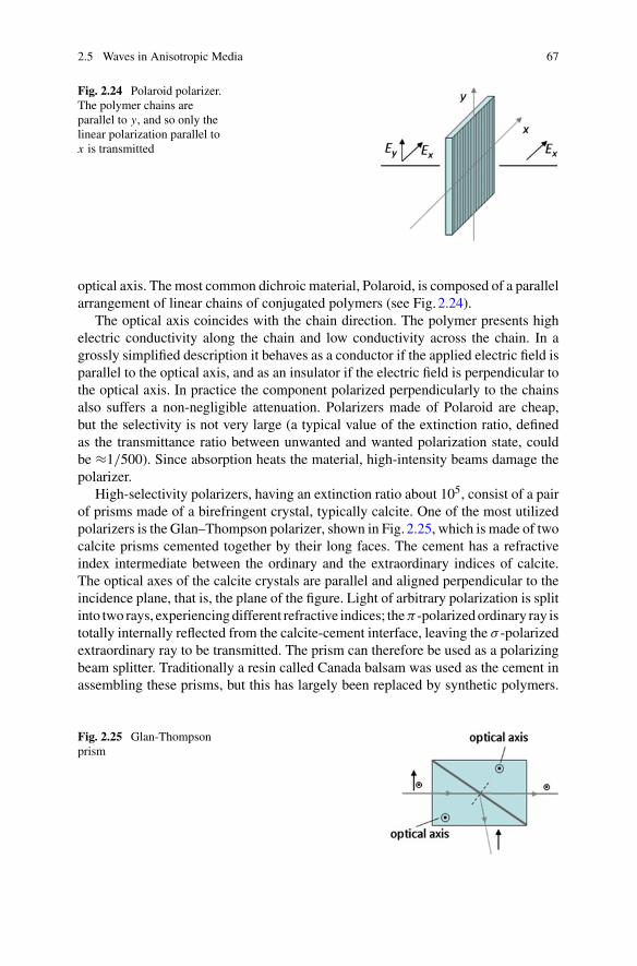
2.5 Waves in Anisotropic Media 67
Fig. 2.24 Polaroid polarizer.The polymer chains areparallel to y, and so only thelinear polarization parallel tox is transmitted
optical axis. The most common dichroic material, Polaroid, is composed of a parallelarrangement of linear chains of conjugated polymers (see Fig. 2.24).
The optical axis coincides with the chain direction. The polymer presents highelectric conductivity along the chain and low conductivity across the chain. In agrossly simplified description it behaves as a conductor if the applied electric field isparallel to the optical axis, and as an insulator if the electric field is perpendicular tothe optical axis. In practice the component polarized perpendicularly to the chainsalso suffers a non-negligible attenuation. Polarizers made of Polaroid are cheap,but the selectivity is not very large (a typical value of the extinction ratio, definedas the transmittance ratio between unwanted and wanted polarization state, couldbe ≈1/500). Since absorption heats the material, high-intensity beams damage thepolarizer.
High-selectivity polarizers, having an extinction ratio about 105, consist of a pairof prisms made of a birefringent crystal, typically calcite. One of the most utilizedpolarizers is the Glan–Thompson polarizer, shown in Fig. 2.25, which is made of twocalcite prisms cemented together by their long faces. The cement has a refractiveindex intermediate between the ordinary and the extraordinary indices of calcite.The optical axes of the calcite crystals are parallel and aligned perpendicular to theincidence plane, that is, the plane of the figure. Light of arbitrary polarization is splitinto two rays, experiencingdifferent refractive indices; theπ -polarizedordinary ray istotally internally reflected from the calcite-cement interface, leaving the σ -polarizedextraordinary ray to be transmitted. The prism can therefore be used as a polarizingbeam splitter. Traditionally a resin called Canada balsam was used as the cement inassembling these prisms, but this has largely been replaced by synthetic polymers.
Fig. 2.25 Glan-Thompsonprism

68 2 Optical Components and Methods
Fig. 2.26 Birefringent plate
The Glan-Thompson polarizer operates over a very wide wavelength range, from350nm to 2.3µm. This type of polarizer can handle much higher optical powersthan the dichroic polarizers.
Thin plates made of a birefringent crystal are used to change the polarization stateof a light beam. The plate faces are parallel to the x-z plane, and the light beamtravels in the y direction, perpendicular to the optical axis z, as shown in Fig. 2.26.If the incident beam is linearly polarized in the x direction (ordinary wave), thenthe propagation across the plate does not modify the polarization state, but simplyintroduces a phase shift Δφo = 2πnod/λ, where d is the plate thickness. Similarly,no modification of the polarization state occurs for the beam polarized along z,which is phase-shifted by: Δφe = 2πned/λ. An input wave linearly polarized in anarbitrary direction can be described as the sum of an ordinary and an extraordinarywave. The two waves are initially in phase, but acquire, on crossing the plate, a phasedifference Δφ = 2π(ne − no)d/λ. In general, the output polarization is elliptical.An important particular case is a birefringent plate that gives a phase difference of|Δφ| = π . This is known as a half-wave plate. When linearly-polarized light isincident upon a half-wave plate, the emergent light is also linearly-polarized. If thepolarization direction of the incident lightmakes an angleα with the optical axis, thenthe polarization direction of the emergent beam makes an angle −α with the sameaxis, therefore the direction of polarization has been rotated through an angle 2α, asshown in Fig. 2.27. A plate for which |Δφ| = π/2 is called a quarter-wave plate.When linearly-polarized light is incident upon a quarter-wave plate, the emergentlight is in general elliptically polarized. If, however, α = π/4, the emergent light iscircularly polarized.
2.5.2 Jones Matrices
The propagation of polarized light beams trough anisotropic optical elements isconveniently described by using the Jones formalism, in which the electric field ofthe light wave is represented by a two-component vector and the optical element bya 2 × 2 transfer matrix.

2.5 Waves in Anisotropic Media 69
Fig. 2.27 Rotation of thepolarization direction in ahalf-wave plate
In general, the electric field of a monochromatic plane wave propagating along zcan be described as the sum of two components:
E(z, t) = Exexp[−i(ωt − kz + φx )]x + Eyexp[−i(ωt − kz + φy)]y, (2.130)
where x and y are unit vectors, directed along x and y, respectively. Equation (2.130)can be written as:
E(z, t) = Eoexp[−i(ωt − kz + φx )]V, (2.131)
where Eo =√
Ex2 + Ey
2, and V is the Jones vector represented by the columnmatrix: (
cosαeiφ sin α
), (2.132)
where α = arctan(Ey/Ex ) and φ = φy − φx .The adopted sign convention considers the angles measured counter-clockwise as
being positive.The vector (2.132) corresponds to a generic elliptical polarization. If the wave is
linearly polarized, φ = 0. The following Jones vectors describe a linearly polarizedfield with a polarization direction forming the angle α with the x axis, or directedalong the x axis, or along the y axis, respectively:
(cosαsinα
);
(10
);
(01
). (2.133)
For a circularly polarized wave, α = π/4 and φ = ±π/2. Therefore the Jonesvectors associated with clockwise and counter-clockwise circular polarization arerespectively given by:
1√2
(1i
); 1√
2
(1−i
). (2.134)
Two waves represented by the vectors V1 and V2 have orthogonal polarizationstates if the scalar product of the two vectors is zero. As an example, the linear

70 2 Optical Components and Methods
polarization states along x and y are mutually orthogonal. An arbitrary polarizationstate can always be described as the sum of two orthogonal polarization states.
An optical component modifying the polarization state of an incident beam isdescribed by a transfer matrix T. If Vi represents the incident wave, then the Jonesvector of the emergent wave is given by: Vu = TVi. If the beam goes through asequence of components with matrices T1, . . . , Tn, then the emergent wave is givenby: Vu = Tn . . . T1Vi. Note that, in general, the T matrices do not commute.
The polarizers having optical axis along x and y are represented, respectively, bythe matrices Tpx e Tpy:
Tpx =(1 00 0
); Tpy =
(0 00 1
). (2.135)
The birefringent plate having optical axis directed along x introduces a phaseshift Δφ between the x and y components of the electric field, without modifyingthe amplitude ratio Ex/Ey . It is represented by:
Tr =(1 00 exp(iΔφ)
). (2.136)
The phase shift is given byΔφ = 2π(ne −no)d/λ, where d is the plate thickness.The half-wave plate corresponds to Δφ = π , and the quarter-wave plate to Δφ =π/2.
The polarization rotation matrix,
R(θ) =(cosθ −sinθsinθ cosθ
), (2.137)
represents an optical component that rotates the polarization direction. If the incidentwave is linearly polarized at an angle θ1, the emergent wave is linearly polarized atthe angle θ2 = θ1 + θ .
It is important to take into account that Jones vectors and matrices change whenthe coordinate system is changed. If a field is described by the vector V, once thecoordinate system is rotated by the angle θ , the same field is described by the newvector V′:
V′ = R(−θ)V. (2.138)
A polarizer having its optical axis that forms an angle θ with the x axis is repre-sented by the matrix:
Tpθ = R(θ)TpxR(−θ) =(
cos2θ sinθcosθsinθcosθ sin2θ
). (2.139)
Similarly, the matrix describing an optical retarder (birefringent plate) having theoptical axis rotated by θ with respect to x is written as:

2.5 Waves in Anisotropic Media 71
Trθ = R(θ)TrR(−θ)
=(1 + [exp(iΔφ) − 1]sin2θ [1 − exp(iΔφ)]sinθcosθ[1 − exp(iΔφ)]sinθcosθ exp(iΔφ) − [exp(iΔφ) − 1]sin2θ
). (2.140)
2.5.3 Rotatory Power
Certain materials present a particular type of birefringence: the two fundamentalmodes of propagation are circularly rather than linearly polarized waves, with right-and left-circular polarizations traveling at different velocities, c/n+ and c/n−. Thisproperty, known as optical activity, is typical of materials having an intrinsicallyhelical structure at the molecular or crystalline level.
As mentioned in Sect. 1.3, a linearly polarized wave can be decomposed into thesum of two circularly polarized waves having the same amplitude. By using Jonesmatrices, one can write:
(cosθsinθ
)= 1
2exp(−iθ)
(1i
)+ 1
2exp(iθ)
(1−i
). (2.141)
If L is the thickness of the optically active medium, the phase delay between thetwocircularly polarizedwaves is givenby:φ = 2π L(n+−n−)/λ. The recombinationof the two emergent waves produces a linearly polarized beam (see Fig. 2.28) with apolarization direction rotated with respect to that of the incident beam:
1
2exp(−iθ)
(1i
)+ 1
2exp[i(θ − φ)]
(1−i
)
= exp(−iφ/2)
(cos(θ − φ/2)sin(θ − φ/2)
). (2.142)
The rotation per unit length, called rotatory power ρ, is:
ρ = φ
2L= π(n+ − n−)
λ. (2.143)
Fig. 2.28 Rotatory power

72 2 Optical Components and Methods
A typical optically active crystal is quartz. For propagation along the optical axis,the rotatory power is 4 rad/cm at λ = 589 nm. Also disordered media containingchiral molecules, as, for instance, sugar molecules, can show optical activity. Foran aqueous solution containing 0.1 g/cm3 of sugar, ρ = 10−2 rad/cm. The sugarconcentration can therefore be determined by measuring the rotatory power.
From a formal point of view, the optical activity can be explained only assumingthe presence of anti-symmetric off-diagonal terms inside the εi j matrix. Such apresence would contradict the assertion that the matrix εi j is symmetric. However, itcan be shown that such a symmetry property applies only for spatially homogeneousfields, that is, infinite wavelength fields. If λ is finite, the local value of D depends,in general, on E and its spatial derivatives. At first order:
Di = εo
∑
jm
(εi j E j + iγi jm
∂ E j
∂xm
). (2.144)
whereas εi j is symmetrical, the third-order tensor γi jm is anti-symmetrical withrespect to the indices i j : γi jm = −γ j im . If there is no absorption, then γi jm isreal. In the case of an incident plane wave with wave vector k, it is found that∂ E j/∂xm = i E j km . Hence:
Di = εo
∑
jm
(εi j E j + iγi jm E j km
). (2.145)
D is related to E by the new electric permittivity tensor:
ε′i j = εi j + i
∑
m
γi jmkm, (2.146)
which is the sum of a symmetric and an anti-symmetric term, the latter vanishing ifthe modulus of k vanishes, that is, if the wavelength becomes infinite.
For an isotropic medium, (2.145) becomes:
Di = εo[εr Ei + iγ (E × k)i ], (2.147)
where (E × k)i denotes the i-th component of the cross product, and γ is a scalarquantity. Assuming k parallel to z, the D components along x and y, as derived from(2.147), are:
Dx = εo[εr Ex + iγ k Ey] (2.148)
Dy = εo[εr Ey − iγ k Ex ]. (2.149)
These two equations show that a linear polarization cannot propagate unchangedinside an optically activemedium, due to the fact that Ex generates Dy , and viceversa.Considering that the electric field of a right- (left-) circularly polarized beam iswritten

2.5 Waves in Anisotropic Media 73
as: E± = Ex ± i Ey , by using (2.148) and (2.149) the quantities D± = Dx ± i Dy
may be written as:D+ = εo[εr + γ k]E+ (2.150)
D− = εo[εr − γ k]E− (2.151)
These two equations show that circular polarization indeed represents a propaga-tion mode inside the optically active medium. The refractive indices seen by the twocircular polarizations are: n± = √
εr ± γ k. Assuming that the second term undersquare root is much smaller than the first one, putting k = nω/c and εr = n2,one obtains the approximate relation: n± = n[1 ± γ k/(2)], and, consequently,ρ = πγ k/(nλ).
2.5.4 Faraday Effect
There are various means to change the optical properties of a medium by applyingan external field. In this section the magneto-optic effect known as Faraday effect isdescribed. It consists in the induction of rotatory power through the application ofa static magnetic field. The effect is longitudinal, since the applied magnetic fieldB is parallel to the propagation direction of the linearly-polarized optical wave. Thepolarization direction is rotated by an angle θ = CV BL , where L is the propagationlength and CV is the Verdet constant. The sign of θ changes with the sign of B, but itdoes not change by reversing the propagation direction. Therefore the rotation effectis doubled if the beam travels back and forth inside the medium.
In the standard configuration of the Faraday rotator the medium has a cylindricalshape and is placed inside a solenoid. The longitudinal magnetic field is created byan electric current flowing into the solenoid.
In the presence of the magnetic field, the relation between D and E can be written,similarly to (2.144), as:
D = εo[εr E + iγB(B × E)], (2.152)
where γB is called magneto-gyration coefficient. The rotatory power is given by:
ρ = CV B = −πγB B
nλ. (2.153)
Thebig difference between apassive rotator, such as a quartz plate, and theFaradayrotator is made clear by considering the situation in which the wave transmitted inone direction is reflected back and retransmitted in the opposite direction. In thecase of the passive rotator there is no net polarization rotation because the rotationgenerated in the forward path is canceled during the backward path, while in the

74 2 Optical Components and Methods
case of the Faraday rotator the effect is doubled. The Faraday rotator is said to be anonreciprocal device.
The Faraday effect can be found in gases, liquids, and solids. Since itsmicroscopicorigin is connected to the Zeeman effect, theVerdet constant becomes largerwhen thewavelength of the optical wave gets close to absorption lines. The most commonlyutilizedmaterials are doped glasses and crystals, like YIG (yttrium iron garnet), TGG(terbium gallium garnet) and TbAlG (terbium aluminum garnet). As an example, theVerdet constant of TGG is: CV = −134 rad/(T · m) at λ = 633 nm, and becomes−40 rad/(T · m) at λ = 1064 nm.
There are some ferromagnetic materials (containing Fe, Ni, Co) that exhibit largevalues of CV , but they also have a very large absorption coefficient, so the Faradayrotation can only be observed in reflection. They have an important application inoptical memories, as will be mentioned in Chap. 8.
2.5.5 Optical Isolator
An optical isolator is a device that transmits light in only one direction, therebypreventing reflected light from returning back to the source. Isolators are utilized inmany laser applications, since back-reflected beams often have deleterious effectson the operating conditions of optical devices.
A Faraday isolator may be constructed by placing a Faraday rotator between twopolarizers, as shown in Fig. 2.29. The optical axis of polarizer 1 is along x , the Faradaycell rotates clockwise the polarization direction by π/4, the optical axis of polarizer2 makes a π/4 angle with the x axis, so that the forward traveling wave is fullytransmitted by the device. If a portion of the transmitted wave is back-reflected by a
Fig. 2.29 Faraday isolator

2.5 Waves in Anisotropic Media 75
subsequent optical component, it travels inside the isolator in the backward direction.Assuming that reflection does not alter the polarization state, the reflected beam isfully transmitted by polarizer 2, and its polarization direction suffers a clockwiserotation of π/4 by the Faraday cell. The backward beam becomes y-polarized, andtherefore is blocked by polarizer 1.
The behavior of the isolator can be mathematically described by Jones matrices.Let Vi and Vu be the Jones vectors of the incident and emergent waves, respec-tively, and call T1, T2, T3, the matrices representing polarizer 1, Faraday rotator, andpolarizer 2, respectively. It is important to recall that all vectors and matrices mustbe expressed with reference to the same x-y coordinate system. The output field isrelated to the input field by the following expression:
Vu = T3T2T1Vi
=(1/2 1/21/2 1/2
)(√2/2 −√
2/2√2/2
√2/2
)(1 00 0
)(10
)=
(√2/2√2/2
). (2.154)
As expected, the emergent wave is linearly polarized at π/4 with respect to thex axis. The back-reflected beam crosses the sequence of devices in opposite order,and is completely blocked by the isolator:
V′u = T1T2T3Vu =
(00
). (2.155)
Note that T3 seems to have no role in the proposed scheme. In practice, however,it may happen that back-reflection modifies the polarization state. In such a case therole of polarizer 2 becomes important.
Fig. 2.30 Faraday isolator including a half-wave plate

76 2 Optical Components and Methods
The sequence of a Faraday rotator plus a half-wave plate constitutes anothernonreciprocal device, as schematically depicted in Fig. 2.30. If the former rotatesthe polarization direction by π/4, and the latter by −π/4, a linearly polarized beamdoes not change its polarization state by crossing the device. On the contrary, for abeam coming from the opposite direction, the two rotations have the same sign, sothat its polarization direction is rotated by π/2. Such a device can be used to makeuni-directional the wave propagation in a circular path.
2.6 Waveguides
Waveguides are strips of dielectric material embedded in another dielectric materialof lower index of refraction. Starting from the advent of optical communications, thedevelopment of integrated optical systems has become more and more important. Insuch systems the light propagates in a confined regime through optical waveguides,instead of free space, without suffering from the effect of diffraction.
A light beam traveling in a direction that is only slightly tilted with respect to theguide axis is totally reflected at the boundary between the two media, provided theincidence angle is larger than the limit angle. So that the guide can completely trapa light beam in a diffraction-less propagation: the optical power should be mainlyconfined inside the guide, with only an evanescent tail extending outside.
Many aspects of guided propagation can be understood by studying the simplecase of a planar dielectricwaveguide, consisting of a slab of thickness d and refractiveindex n1, usually called core, surrounded by a cladding of lower refractive index n2,as shown in Fig. 2.31. In a planar waveguide, confinement is guaranteed only in onedimension. Light rays making angles θ with the z-axis, in the x-z plane, undergototal internal reflection if cosθ ≥ n2/n1. The electromagnetic theory predicts theexistence of waveguide modes, that is, transverse field distributions that are invariantin the propagation. Here, the discussion is limited to waves linearly polarized alongx , that is, to transverse electric-field modes (TE modes). The propagation propertiesare derived by writing the Helmholtz equation inside the two media,
Fig. 2.31 Scheme of aplanar waveguide

2.6 Waveguides 77
(∇2 + (n1ko)2)E(r) = 0 (2.156)
(∇2 + (n2ko)2)E(r) = 0, (2.157)
and imposing the boundary conditions.By assuming that the wave propagates along z with a propagation constant β, the
electric field can be generally written as:
E(x, z, t) = A(x)exp[i(βz − ωt)] (2.158)
By substitution of (2.158) into (2.156), the equation relative to medium 1 (thecore) becomes:
d2A
dx2+ [(n1ko)
2 − β2]A(x) = 0. (2.159)
Similarly, inside the cladding:
d2A
dx2+ [(n2ko)
2 − β2]A(x) = 0 (2.160)
Since the propagation constant of the guided wave must be intermediate betweenn2ko and n1ko, the solution of (2.159) is a periodic function, A1 cos(γ1x), and thatof (2.160) is an exponential function, A2exp(−γ2x), where the real quantities γ1 andγ2 are given, respectively, by:
γ1 =√
n12ko
2 − β2, (2.161)
and
γ2 =√
β2 − n22ko
2 (2.162)
By imposing the continuity of the field amplitude and its derivative at x = d/2,it is found:
A1 cos(γ1d/2) = A2 exp(−γ2d/2), (2.163)
andA1γ1 sin(γ1d/2) = A2γ2 exp(−γ2d/2). (2.164)
Non-zero field amplitudes A1 and A2 exist only if the following condition issatisfied:
tan(γ1d/2) = γ2
γ1. (2.165)
This is a transcendental equation in the variable β. A graphic solution can befound by plotting the right- and left-hand sides as functions of β.

78 2 Optical Components and Methods
What has been calculated is the propagation constant of the fundamental mode. Itcan be shown that the waveguide can support a discrete sequence of modes, whosepropagation constants are derived by generalizing (2.165) as follows:
tan(γ1d/2 − mπ/2) = γ2
γ1, (2.166)
where m = 0, 1, . . ..Whereas a solution always exists for the fundamental mode, a value of the propa-
gation constant β1 of the m = 1 mode satisfying the condition n2ko ≤ β1 ≤ n1ko isfound only if the mode frequency ν is larger than the cut-off frequency νc given by:
νc = c
2d√
n12 − n2
2, (2.167)
By increasing the mode order m, the cut-off frequency increases. Therefore, byincreasing the frequency, the guide accepts more and more propagation modes.According to (2.167), to be single-mode the waveguide must be thin, and the refrac-tive index difference n1 − n2 needs to be small. As it will be seen in the followingchapters, there are various applications requiring single-mode propagation.
Concerning the field distribution of the waveguide modes, it should be noted that,by increasing m, the field penetrates deeper into the cladding. Correspondingly, thepropagation constant βm decreases with m.
Most of the considerations developed for the propagation in slab waveguides alsoapply for the case of channel waveguides, in which the confinement of the light beamis guaranteed on two dimensions. A very important example of channel waveguideis the optical fiber (Fig. 2.32a), which is a waveguide with a cylindrical symme-try that will be discussed in greater details in Chap.6. Figure2.32b–d illustrate thetypical geometries of different channel waveguides fabricated on planar substrates,which constitute the basic structures of several integrated optical devices, like opticalmodulators (Chap.4) and semiconductor lasers or amplifiers (Chap.5). In the recentyears, the evolution of communication systems has driven the development of opti-cal circuits mainly based on silicon deposited on silicon oxide (silicon on insulator,SOI) in which several electronic and photonic functions are integrated on the same
Fig. 2.32 Scheme of themost commonly used opticalwaveguide geometries:a optical fiber, b embeddedwaveguide, c rib waveguide,d ridge waveguide. Thedarker regions represent thecores in which the light isconfined

2.6 Waveguides 79
chip. Miniaturization is a key issue for this application, as it will be discussed inSect. 8.1.3, and waveguides with cross-sections of hundreds of nanometers and veryhigh refractive contrast are needed. This provides high confinement of the light thatcan be bent in curved waveguides, thus making feasible the fabrication of complexnetworks of waveguides on a very small area.
Problems
2.1 Given that the wavelength of a light signal in vacuum is 600nm, what will it bein a glass block having a refractive index n = 1.50?
2.2 A glass block having an index of 1.55 is coated with a layer of magnesiumfluoride of index 1.32. For light traveling in the glass, what is the total reflectionangle at the interface?
2.3 Yellow light from a sodium lamp (λ = 589 nm) traverses a tank of benzene (ofindex 1.50), which is 30-m long, in a time τ1. If it takes time τ2 for the light to passthrough the same tank when filled with carbon disulfide (of index 1.63), determinethe value of τ2 − τ1.
2.4 Light having a vacuum wavelength of 600 nm, traveling in a glass (n = 1.48)block, is incident at 45◦ on a glass-air interface. It is then totally internally reflected.Determine the distance into the air at which the amplitude of the evanescent wavehas dropped to a value of 1/e of its maximum value at the interface.
2.5 A beam of light in air strikes the surface of a transparent material having anindex of refraction of 1.5 at an angle with the normal of 40◦. The incident light hascomponent E-field amplitudes parallel and perpendicular to the plane-of-incidence of10 and 20V/m, respectively. Determine the corresponding reflected field amplitudes.
2.6 The complex index of refraction of silver at λ = 532nm is n′ + in′′ = 0.14 −3.05i . Calculate: (i) the reflectance of an air-silver surface at normal incidence; (ii)the transmittance of a 100µm silver plate.
2.7 A Gaussian beam at wavelength λ = 0.63 µm having a spot size at the beamwaist of wo = 0.5 mm is to be focused to a spot size of 30 µm by a lens positionedat a distance of 0.5m from the beam waist. What focal length should the lens have?
2.8 A Gaussian beam with λ = 800nm and wo = 0.1mm at z = 0 is propagatingalong the z axis. A plano-convex lens, made of a spherical glass cap having a radiusof curvature of 4 cm, is placed at z1 = 20cm. The refractive index of the glass isn = 1.8. Determine: (i) at which coordinate z2 the beam is focused; (ii) the beamspot size at z2; (iii) the lens diameter to be chosen in order to collect 99% of thebeam power.

80 2 Optical Components and Methods
2.9 A blazed reflection grating with pitch d = 1200nm and blazing angle θg =20◦ is used in the Littrow configuration. Determine which incident wavelength isdiffracted at second order in the backward direction.
2.10 A Fabry-Perot interferometer made by two identical mirrors at distance d =1mm is illuminated by a light beam containing two wavelengths λ1 = 1064nm andλ2 = λ1 + Δλ, where Δλ = 0.05nm. Determine which is the minimum reflectanceof the two mirrors required to obtain a resolving power Pr ≥ λ1/Δλ.
2.11 Consider a light beam at λ = 589nm traveling along the z-axis and linearlypolarized along the x-axis. The light beam crosses, in succession, a quarter-waveplate and a polarizer. The optical axis of the quarter-wave plate is in the x-y plane,forming an angle π/4 with the x-axis. The optical axis of the polarizer is parallelto the y-axis. Write the Jones matrix of the quarter-wave plate in the x-y referenceframe, and calculate the fraction of the incident power that is transmitted by thepolarizer.
2.12 Consider the following sequence of components: a polarizer P1, a Faradayrotator that rotates counterclockwise the linear polarization direction of the incomingbeam by 45◦, a calcite half-wave plate, and a second polarizer P2. Assume thatthe incoming beam travels along y and is linearly polarized along x , that the twopolarizers have optical axes parallel to x , and that the optical axis of the calcite platelies in the x-z plane. (i) Calculate which angle the optical axis of the plate shouldform with the x axis in order to ensure a unitary transmission. (ii) Write the Jonesmatrix of the half-wave plate in the x-z reference frame.

Chapter 3The Laser
Abstract All the light sources utilized before the invention of the laser are basedon spontaneous emission processes from excited atoms. Since each atom emits in arandom direction with a random phase, conventional light sources are intrinsicallychaotic. The laser is a completely different light source, because it is based on stim-ulated emission instead of spontaneous emission, which means that atoms emit in acooperative way, generating amonochromatic and collimated light beam. The funda-mental ingredient for making a laser is the optical amplifier. A mechanism selectingwavelength and direction is provided by the positive feedback that transforms theamplifier into an oscillator. In this chapter, after shortly mentioning conventionallight sources, especially thermal sources, and after giving a brief historical introduc-tion to the laser, the general scheme of the oscillator is first discussed. Successively,by using an elementary treatment of the interaction between light and atoms, theconditions under which a set of atoms can become an optical amplifier are derived.After discussing the general laser scheme, the steady-state and pulsed behavior ispresented, together with a concise description of a few solid-state and gas lasers. Thechapter ends with a comparison between the laser and the conventional light source.
3.1 Conventional Light Sources
Conventional light sources, like flames, incandescent lamps, and electric dischargelamps, operate by converting an input energy (chemical, thermal, and electrical,respectively) to light. The light is emitted over the full solid angle, usually witha very broad frequency spectrum, except for the case of low gas-pressure electricdischarge lamps. The main application of these sources is to provide illumination,in substitution to the Sun.
It is of historical importance to discuss the emission of incandescent sources,such as the Sun (which converts nuclear energy from fusion reactions into light), ora common household tungsten-filament lamp. The study of the emission spectrumfrom these incandescent sources and of its dependence on the absolute temperature Thas had a profound impact on modern physics. In the theoretical treatment proposedduring the nineteenth century, an ideal body consisting of a closed cavity kept in
© Springer International Publishing Switzerland 2016V. Degiorgio and I. Cristiani, Photonics, Undergraduate Lecture Notes in Physics,DOI 10.1007/978-3-319-20627-1_3
81

82 3 The Laser
thermal equilibrium at temperature T was considered, under the assumption that theinner walls of the cavity could emit radiation at all possible frequencies. By using ageneral thermodynamic argument, Kirchhoff demonstrated that the spectrum of the“blackbody” radiation from such a cavity depends only on T , and is independentof the nature of the material or the shape of the cavity. Defining ρ(ν, T )dν as thedensity of electromagnetic energy inside the cavity in the frequency interval betweenν and ν + dν, a very strong inconsistency between predictions based on Maxwellequations and experimental observations of ρ(ν, T ) was discovered. By making therevolutionary assumption that the energy of the dipole oscillating at frequency ν canonly take discrete values that are multiples of the fundamental quantum hν, Planckwas able to provide the solution to this problem in 1901, obtaining the followingexpression:
ρ(ν, T ) = 8πhν3
c31
exp(hν/kB T ) − 1. (3.1)
Besides the Boltzmann constant of kB = 1.38× 10⁻²³ J ·K−1, (3.1) contains thenew universal constant of h, called Planck constant, having value 6.55× 10⁻³⁴ J · s.
By making the derivative of (3.1), one finds that the frequency νm correspondingto the maximum value of ρ(ν, T ) is proportional to T , following the approximaterelation: νm ≈ 5kB T/h.
Introducing the peak wavelength λm = c/νm , expressing λm in meters e T inKelvin, the following relation, usually called Wien’s law, is obtained:
λm T = 0.288 × 10⁻² m · K. (3.2)
Figure3.1 shows the blackbody emission spectra of the Sun (5500K) and atungsten-filament lamp (1500K). In the first case the peak of the emission is inthe visible range, whereas in the second case a large portion of the emitted radiationis in the infrared, indicating that the incandescent lamp is a low-efficiency source ofvisible light.
Fig. 3.1 Blackbody emission spectra, as calculated for the Sun (T = 5500K) and for a tungsten-filament lamp (T = 1500K). The two curves are normalized to the same maximum value
3.1 Conventional Light Sources 83
The electric-discharge lamp, also known as the fluorescent lamp, uses electroncollisions to generate the atomic excitation for light emission. Notwithstanding thefact that the working temperature can be much lower, this approach provides a higherconversion efficiency of electrical power to visible light power than incandescentsources.
3.2 Origins of the Laser
Whereas traditional light sources consist of a collection of independently emittingatoms, the laser is a source in which individual emitters have a correlated phase andalso well defined emission direction.
In an important paper published in 1916 Einstein considered a blackbody cavityin thermal equilibrium containing a set of two-level atoms, and showed that thebalance between absorption and emission processes becomes compatible with theblackbody law only if one assumes the existence of a previously unknown process,called stimulated emission. At that time, it was not noted that this new process canresult in optical amplification. It took a further four decades before proposals aimedat using stimulated emission to amplify optical beams were put forward.
The first amplifier based on stimulated emission, called maser (acronym of“Microwave Amplification by Stimulated Emission of Radiation”), used ammoniamolecules in a high magnetic field, and had emission in the microwave frequencyrange, at 23.87GHz. The experiment was performed at the Columbia University,New York, by Gordon, Zeiger and Townes in 1954. They sent a beam of excitedammonia molecules into a resonant cavity, obtaining a self-sustaining emission. Amaser amplifier had an important role in the first demonstration of long-distancecommunications using the reflection of a microwave signal from an orbiting satellitein space. In this experiment, performed by a Bell Labs team led by Pierce in 1960,a maser was used as a very sensitive low-noise device to amplify the faint signalscoming from the satellite.
The fundamental step for the birth of Quantum Electronics (this was the initialname given to this new field) was the invention in 1960 of the first oscillator emittingvisible light, the ruby laser, created by Maiman, a researcher working at the HughesResearch Laboratories in California. Such a realization had been prepared by thetheoretical studies of Townes in the United States, and Basov and Prokhorov inRussia, studies that were awarded the Nobel Prize in 1964. The acronym “laser”comes from maser, with the substitution of “light” for “microwave”. The laser isindeed an oscillator, even if the acronym laser (Light Amplification by StimulatedEmission of Radiation) seems to describe an amplifier.
Starting from 1960, Photonics (this is the name nowmore frequently used insteadof Quantum Electronics) had a very rapid development. In a few years, laser actionwas demonstrated in a wide variety of solid, liquid, and gaseous materials. A turningpointwas the invention in 1962 of the semiconductor laser; a very small device havinghigh efficiency and long operating lifetime, which can be fabricated using the same

84 3 The Laser
technology developed for integrated electronic circuits and devices. Normally everytype of laser emits one (or more) well-defined wavelengths that are characteristicof the material used for amplification. A very important property of semiconductorlasers is that they can be designed to work at a pre-selected wavelength, by tuningthe chemical composition of the active layer.
3.3 Properties of Oscillators
An oscillator is a device that generates a sinusoidal signal with a stable amplitude andfixed frequency. The capability of producing oscillating electric fields at higher andhigher frequencies has played a basic role in the development of telecommunicationsystems, of computers, and, in general, of all electronic instrumentation. The laseris a device that extends the working principle of the electronic oscillator to opti-cal frequencies. The analogy with the electronic device is conceptually important,because it explains at first glance the different emission properties of a laser withrespect to traditional light sources. At the same time, the analogy immediately sug-gests that lasers can play a very important role in the information and communicationtechnology.
In this section the general properties of oscillators are discussed, showing that anoscillating output signal can be generated by a scheme involving the combination ofamplification with positive feedback. The discussion is developed generally, withoutspecifying the exact nature of the signal. The description of the optical amplifier andthe corresponding oscillator is deferred to the following sections.
In the block scheme presented in Fig. 3.2, the input and output signals Si e Su
may represent a displacement in the case of the mechanical oscillator, a voltage forthe electronic oscillator or an electric field for a microwave or optical oscillator. Theinput signal Si goes through an amplifier with gain G. The fraction β of the amplifieroutput is fed back and added to Si . Therefore, in the stationary regime, the outputsignal Su is given by:
Su = GSi + βG2Si + β2G3Si + · · · (3.3)
Fig. 3.2 General scheme of the oscillator: amplifier with positive feedback

3.3 Properties of Oscillators 85
By assuming that |βG| < 1, the geometric series represented by (3.3) is conver-gent. One obtains:
Su = SiG
1 − βG. (3.4)
The quantity βG is called loop gain. The transfer function of the amplifier withfeedback, defined as the ratio between output and input, is given by:
T = Su
Si= G
1 − βG. (3.5)
The signal Si is taken as a sinusoidal function of time with angular frequency ω.Generally speaking, both G and β are complex functions of ω. In order to make thetreatment more explicit, assume that β is independent of ω and that the frequencydependence of G has a resonance at ωo:
G(ω) = Go
1 + i(ω − ωo)τ(3.6)
The power amplification |G(ω)|2 is:
|G(ω)|2 = |Go|21 + (ω − ωo)2τ 2
(3.7)
The function (3.7) is a Lorentzian (from Lorentz), and represents the effectivebehavior of absorption (or gain) as a function of the angular frequency in mostpractical cases. The quantity τ−1 is the half-width at half-height of the Lorentzianfunction.
Through substitution of (3.6) inside (3.5), one finds the transfer function of thesystem with feedback:
T (ω) = Go
1 + i(ω − ωo)τ − βGo= G f o
1 + i(ω − ωo)τ f, (3.8)
where G f o = Go/(1 − βGo), and τ f = τ/(1 − βGo). It is evident that positivefeedback increases the peak gain, and, at the same time, decreases the frequencyband, such that the product between frequency band and peak gain is left unchanged.Figure3.3 shows the behavior of the power transfer function, |T (ω)|2, for increasingvalues of the loop gain, within the interval 0 < βGo < 1.
For βGo tending to 1, Gfo tends to infinity and the bandwidth Γ f = 2τ−1f tends
to 0. The condition βGo = 1 is the threshold condition for the operation of theoscillator: in fact, if G f o becomes infinite, the system can provide a finite outputsignal even if the input is infinitesimal.
What kind of output signal is generated by such an oscillator? Since the bandwidthbecomes infinitely narrow around ωo, the output signal must be a sinusoidal oscilla-tion at frequency ωo. In the general case, in which β also depends on ω, the angular

86 3 The Laser
Fig. 3.3 Behavior of thefrequency response of theamplifier with positivefeedback for various valuesof the loop gain
frequency corresponding to maximum loop gain can be different fromωo. If the loopgain is larger than 1, the oscillation is triggered by the noise always present insidea real-world loop: from amongst all the noise frequency components, the systempreferentially amplifies the component with angular frequency ωo.
The treatment developed thus far would indicate that the output signal Su iscontinuously growing when the gain is above the threshold value Goth = β−1.This is clearly impossible, because it would violate energy conservation. Since thesupply power of the amplifier has a finite value, the output power must also have afinite upper bound.
The steady-state value of Su can be derived using a treatment that includes nonlin-ear effects. It is a general property of an amplifier that the gain must decrease whenthe amplitude of the output signal becomes large. This effect is called saturation.As shown qualitatively in Fig. 3.4, the gain Go must be a decreasing function of Su ,going to 0 when Su becomes large.
The working operation of an oscillator is as follows: initially the oscillator isdesigned to have a small-signal gain larger than β−1. As long as Su grows through
Fig. 3.4 Saturation of theamplifier: behavior of gain asa function of the outputsignal Su . The working pointof the oscillator is given bythe condition βGo(Sus) = 1

3.3 Properties of Oscillators 87
successive amplifications within the loop, the gain Go(Su) decreases: the stationarystate is reached when Su attains the saturation value Sus , in correspondence of whichthe saturated loop gain is equal to 1. By looking at Fig. 3.4 it is evident that, ifSu < Sus the loop gain is >1 so that Su is growing toward the stationary value,whereas, if Su > Sus , the loop gain becomes <1 so that Su is now decreasingtoward the stationary value. The conclusion is that the stable point of the oscillatorcorresponds to the situation in which the saturated loop gain is equal to 1.
3.4 Emission and Absorption of Light
The general discussion of the preceding section shows that the essential ingredientfor building an optical oscillator is the optical amplifier. In this section an elementarydescription of the interactions between atoms and light is presented, as a preliminarystep toward the treatment of the optical amplifier.
An atom is made of a nucleus with a positive electric charge at the center and asurrounding electron cloud of negative electric charge. Viewing the atom as a micro-scopic planetary system, its internal energy can be defined as the sum of the poten-tial energy associated to the spatial distribution of electric charges plus the kineticenergy of the electrons that are undergoing a rotational motion around the nucleus.The configuration of the atom can be determined, at least in principle, by solvingthe Schrödinger equation for the system. Quantum mechanics demonstrates that theinternal energy of the atom can take only discrete values, here called E0, E1, E2 . . .
in increasing order, where E0 is the energy of the equilibrium configuration (groundstate), and E j , with j > 0, is the energy of the j-th excited state. In an intuitivemodel the excited state corresponds to one (or more) electrons having moved fromthe equilibriumorbit to an outer, higher energy, orbit. The atommaymake a transitionfrom its initial state to an upper excited state by absorbing a photon, or it may decayfrom an excited state to a lower-energy state by emitting a photon, but all transitionsmust satisfy the energy conservation relation:
νik = Ei − Ek
h, (3.9)
where Ei > Ek . The atom in the state k can move to the state i by absorbing aphoton, only if it is illuminated by light having frequency νik . Analogously the atomdecaying from state i to state k emits a quantum of light at frequency νik . Each type ofatom has different energy levels, and so it has a different discrete set of characteristicfrequencies νik . It should be mentioned that not all atomic transitions are radiative,i.e., are compatible with the absorption or emission of light. There are quantummechanical selection rules (not discussed here) that determine which transitions areradiative.
It is useful to have in mind the order of magnitude of the energy differencefor atomic transitions associated to visible light. Considering, as an example, light

88 3 The Laser
Fig. 3.5 Absorption and emission processes between levels 0 and 1
with a wavelength of λ = 0.5µm, and frequency ν = c/λ = 6 × 10¹⁴ Hz, thecorresponding energy difference, calculated from (3.9), is 2.5eV.
Consider a box containing Nt identical atoms per unit volume, illuminated by amonochromatic wave with intensity I and frequency ν close to ν10. If the intensityis divided by the photon energy, it gives the photon flux Φ = I/(hν), which is thenumber of photons crossing the unit area in the unit time.
A schematic of the different absorption and emission processes is illustrated inFig. 3.5. Some atoms will absorb a photon moving from the ground level 0 to level1. The number of absorption processes per unit time and unit volume must be pro-portional to the number of available photons and to the number of atoms on level 0.Every absorption reduces by 1 the number of atoms on level 0, therefore:
− d N0
dt= σ01(ν)ΦN0, (3.10)
where N0(t) is the number of atoms per unit volume on level 0 at time t , called thepopulation of level 0 at time t . The minus sign in front of the derivative inside (3.10)indicates that absorption processes decrease the population of level 0.
The proportionality constant σ01(ν), called absorption cross-section, representsthe probability of absorption of a photon by the atom, and has dimensions of an area.Since the energy of the excited atomic levels is always defined with some spread,σ01(ν) is a function of ν that is peaked at ν10, but has a non-zero broadening. It istypically described by a Lorentzian function.
The excited atom goes back to the ground state by spontaneously emitting a pho-ton. The spontaneous emission is spatially isotropic, and has a spectral distributionidentical to that of the absorption cross-section. It is important to point out that theradiation spontaneously emitted by a given atom has no memory of the direction,frequency or phase of the exciting radiation, and that it is uncorrelated with theemission of other nearby atoms.
By assuming that at t = 0 there are some excited atoms on level 1, it is foundthat the intensity of spontaneous emission decays exponentially with time. The timeconstant τ10, which is characteristic of the considered transition, is called lifetimeof the level 1. The reciprocal A10 = τ−1
10 represents the decay probability from 1

3.4 Emission and Absorption of Light 89
to 0 per unit time. Considering that every spontaneous emission reduces the num-ber N1 by 1, and that the number of spontaneous emission processes per unit timeand unit volume is given by A10N1, the decrease of the population of level 1 isdescribed by:
− d N1
dt= A10N1 (3.11)
In 1917 Einstein demonstrated that the presence of quasi-resonant radiation at afrequency close to ν10 stimulates the decay of the excited atom from state 1 to state 0.
In analogy with the absorption process, the number of stimulated emissionprocesses per unit time and unit volume can be written as:
− d N1
dt= σ10(ν)ΦN1, (3.12)
where σ10(ν) is the stimulated emission cross-section, which, as shown in the nextsection, coincides with the absorption cross-section.
If the atoms are at an absolute temperature of T , then the ratio between N1 andN0 is given by the Boltzmann factor:
N1
N0= exp
(−hν10
kB T
). (3.13)
As an example, for a transition in the red light region (hν10 = 2eV) at roomtemperature (T = 300K), it is found: N1/N0 = e−80 ≈ 10−35. This means that theprobability of finding an excited atom is negligible, for a transition in the visible atroom temperature.
If all the atoms are in the lower energy state (i.e., the level 0), a quasi-resonant lightbeam initially generates only absorption processes. If some fraction of the atoms arein level 0, and the rest are in level 1, then a competition arises between absorption andstimulated emission processes. If N0 > N1, absorption prevails. However, if N0 <
N1, then the number of generated photons overcomes the number of absorptions.The condition of N0 < N1 is called the population inversion condition.
The important aspect of the stimulated emission process is that, in contrast to thecase of spontaneous emission, the emitted radiation has the same direction, polar-ization, frequency and phase of the incident radiation. As such, a light beam havinga frequency close to ν10 experiences amplification after passing through a volumecontaining a collection of atoms that are prepared in a state of population inversion.In order to build an optical amplifier, it is necessary to find a means of creating andmaintaining a population inversion.
What happens if a set of two-level atoms is illuminated with a photon flux Φ atfrequency ν10? By combining (3.10), (3.11), and (3.12), and taking into account the
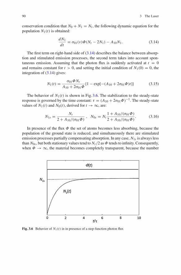
90 3 The Laser
conservation condition that N0 + N1 = Nt , the following dynamic equation for thepopulation N1(t) is obtained:
d N1
dt= σ01(ν)Φ(Nt − 2N1) − A10N1. (3.14)
The first term on right-hand side of (3.14) describes the balance between absorp-tion and stimulated emission processes, the second term takes into account spon-taneous emission. Assuming that the photon flux is suddenly activated at t = 0and remains constant for t > 0, and setting the initial condition of N1(0) = 0, theintegration of (3.14) gives:
N1(t) = σ01ΦNt
A10 + 2σ01Φ{1 − exp[−(A10 + 2σ01Φ)t]} (3.15)
The behavior of N1(t) is shown in Fig. 3.6. The stabilization to the steady-stateresponse is governed by the time constant: τ = (A10 + 2σ01Φ)−1. The steady-statevalues of N1(t) and N0(t), derived for t → ∞, are:
N1s = Nt
2 + A10/(σ01Φ), N0s = Nt
1 + A10/(σ01Φ)
2 + A10/(σ01Φ). (3.16)
In presence of the flux Φ the set of atoms becomes less absorbing, because thepopulation of the ground state is reduced, and simultaneously there are stimulatedemission processes partially compensating absorption. In any case, N1s is always lessthan N0s , but both stationary values tend to Nt/2 asΦ tends to infinity. Consequently,when Φ → ∞, the material becomes completely transparent, because the number
Fig. 3.6 Behavior of N1(t) in in presence of a step-function photon flux

3.4 Emission and Absorption of Light 91
of stimulated emission processes compensates for the absorption processes. The firstof relations (3.16) can be written as:
N1s = Nt
2
1
1 + Φs/Φ(3.17)
where Φs = A10/(2σ10) is the saturation flux for the considered transition.
3.4.1 Einstein Treatment
In his 1917 article, Einstein not only introduced the new concept of stimulated emis-sion, but also derived in a simple way the relations connecting emission and absorp-tion processes. In this section the main steps of the treatment are reproduced.
Einstein considered a set of atoms inside a blackbody cavity at temperature T,observing that, at thermal equilibrium, the number of atoms per unit time makingthe transition from level 0 to level 1 must coincide with the number of atoms makingthe opposite transition. The radiation thermally generated inside the cavity is notat all monochromatic, but it presents a frequency spread comparable or even largerthan the bandwidth Δν10 of the absorption cross-section of the considered atomictransition. In such cases, in order to express the number of absorption processes,one should use, instead of (3.10) that refers to a monochromatic photon flux, thefollowing integral:
d N0
dt= −N0
∫σ01(ν
′)φ(ν′)dν′, (3.18)
where φ(ν′) is now the incident flux per unit frequency. The total incident flux isgiven by the integral:
Φ =∫
φ(ν′)dν′ (3.19)
Of course, (3.18) reduces to (3.10) if the incident flux is monochromatic: φ(ν′) =Φδ(ν′ − ν), where δ(ν′ − ν) is Dirac delta function. In contrast, if the bandwidth ofφ(ν′) is much larger than Δν10, then (3.18) can be approximated as:
d N0
dt= −c−1B01φ(ν10)N0, (3.20)
where
B01 = c∫
σ01(ν′)dν′ (3.21)
is the absorption coefficient (expressed in units: m3s−2).

92 3 The Laser
Balancing spontaneous emission and absorption processes, and introducing theenergy density ρ(ν) = (hν)φ(ν)/c instead of the photon flux, one finds:
hν10A10N1 = ρ(ν10)B01N0 (3.22)
Taking into account that N0/N1 is given by (3.13), (3.22) gives a dependence ofρ(ν) on temperature that, rather surprisingly, is different from the expression (3.1). Atthis point, Einstein made the hypothesis that a third process must be occurring, whichhe called stimulated emission. By expressing the number of stimulated emissionprocesses per unit time with a relation similar to that used for absorption processes,(3.12) transforms into:
d N1
dt= −c−1B10φ(ν)N1 (3.23)
where B10 is the stimulated emission coefficient:
B10 = c∫
σ10(ν′)dν′ (3.24)
The balance between absorption and emission, including now also stimulatedemission, becomes:
hν10A10N1 + ρ(ν10)B10N1 = ρ(ν10)B01N0. (3.25)
From (3.25) the following expression is derived:
ρ(ν10) = hν10A10
B01(N0/N1) − B10. (3.26)
By taking into account (3.13), and comparing (3.26) with (3.1), the followingrelations are obtained:
B10 = B01 ,A10
B01= 8πν10
2
c3(3.27)
Note that the equality B10 = B01 implies that σ10 = σ01.Relations (3.27) show symmetry between absorption and stimulated emission
processes, and demonstrate that the spontaneous emission coefficient A10 is propor-tional to B01. The quantum-mechanical calculation, not discussed here, shows thatB01 is proportional to ν10. As a consequence, A10 is proportional to the cube of thefrequency: this means that the spontaneous decay time τ10 = (A10)
−1 is much longerfor infrared transitions with respect to visible transitions, and becomes very short forUV or soft X-ray transitions. As will be seen, very short decay times of the excitedlevel make it much more difficult to create and maintain a population inversion fora given transition, and so it is comparatively difficult to build optical amplifiers andlasers in the UV or soft X-ray region.

3.5 Optical Amplification 93
3.5 Optical Amplification
In this section it is described how to obtain optical amplification. It is clear from theprevious sections that it is impossible to obtain a steady-state population inversion onthe transition 0–1 using an approach dealing only with levels 0 and 1. The excitationprocess must involve a third level.
Three-level system. The discussion starts by considering a three-level system, likethe one shown in Fig. 3.7. The scheme is the same as that used in the first laser; theruby laser. The aim is to obtain a population inversion between the ground level 0and the excited level 1. In the jargon of Photonics the process producing populationinversion is called pumping process, and the amplifying medium is called activemedium. The idea is to pump with light resonant with the transition between level 0and level 2. In presence of a photon flux Φp(ν) at ν02, absorption processes excitingatoms to level 2 occur. The spontaneous decay from level 2 to level 1 populateslevel 1. Intuitively, one could predict that population inversion can be obtained if thespontaneous decay process from 2 to 1 is quicker than the process from 1 to 0. Ina regime of dynamic equilibrium, this does indeed create a “bottleneck” that favorsthe growth of N1.
The quantitative treatment of the three-level scheme is based on the so-calledrate equations. These describe the population dynamics by taking into account allpossible emission and absorption processes among the three levels:
d N1
dt= A21N2 − A10N1 (3.28)
d N2
dt= W02p(N0 − N2) − (A20 + A21)N2, (3.29)
where A10, A20 and A21 are spontaneous decay probabilities per unit time, and W02p
is the probability per unit time of a transition from level 0 to level 2 under the actionof the pump. Using (3.18), one finds: W02p = ∫
σ02(ν′)φp(ν
′)dν′.
Fig. 3.7 Three- and four-level schemes. The vertical direction indicates increasing energy of theatomic levels

94 3 The Laser
Since the sum of the three populations coincides with the total number of atomsper unit volume Nt :
N0 + N1 + N2 = Nt , (3.30)
N0 can be eliminated from (3.29), so that a systemof two equationswith twounknownfunctions is obtained. If W02p is constant, then the system can be easily solved. Herethe discussion is limited to the steady-state solutions, obtained by putting all thetime-derivatives equal to 0.
The steady-state population inversion is given by:
Ns = N1s − N0s = Nt
1 − A10A21
W02p+A20+A21W02p
1 + A10A21
2W02p+A20+A21W02p
. (3.31)
In order to obtain amplification, Ns should be positive, which means that the signof the fraction appearing at right-hand side of (3.31) must be positive. For very largevalues of the pump parameter, W02p � A20 + A21, it is a necessary condition thatA21 > A10, in agreement with the intuitive considerations mentioned above. It isinteresting to note that, if A21 � A10 and simultaneously W02p � A20 + A21, then(3.31) reduces to Ns = Nt . This means that all the atoms have been excited to level1.
The condition Ns = 0 gives the threshold value of the pump parameter:
W02pth = A10A20 + A21
A21 − A10. (3.32)
To avoid excessive values of W02pth , systems in which A21 is much larger thanA10 are usually chosen. The first laser (i.e., the ruby laser) has the simple three-levelscheme, with A21 many orders of magnitude larger than A10.
Four-level system. Optical amplification can be also achieved by using a four-levelscheme, illustrated in Fig. 3.7. In this scheme, the pump excites the atom from theground level to level 3; level 2 is then populated by the spontaneous decay from 3 to2, and optical amplification occurs between 2 and 1, at a frequency ν21. Intuitivelyit can be expected that population inversion between 2 and 1 can be achieved, if thespontaneous decay time from 3 to 2 is short, from 2 to 1 is long, and from 1 to 0 isshort.
There is an important difference between the three- and four-level schemes. Inthe three-level scheme, the amplifier exploits the transition 1 to 0, in which the lowerlevel is the ground level. As a consequence, in order to reach threshold, which meanszero population inversion, at least half of the atoms must be excited. In the four-levelscheme the amplifier exploits a transition between two excited states. This meansthat, since level 1 is initially empty, a positive population inversion is technicallyachieved when even only one atom is brought to level 2. As a result, the four-level

3.5 Optical Amplification 95
scheme requires much lower pump power with respect to the three-level scheme forlasing, and so most practical lasers operate using a four-level scheme.
The dynamics of the four-level system is described by the following rate equations:
d N3
dt= W03p(N0 − N3) − (A30 + A31 + A32)N3 (3.33)
d N2
dt= A32N3 − (A20 + A21)N2 (3.34)
d N1
dt= A31N3 + A21N2 − A10N1, (3.35)
where W03p = ∫σ03(ν
′)φp(ν′)dν′.
The system (3.33)–(3.35) is completed by:
N0 + N1 + N2 + N3 = Nt . (3.36)
Again, the discussion is limited to the steady-state solutions, by putting all timederivatives equal to 0. The steady-state population inversion is found to be:
Ns = N2s − N1s = Nt(1 − C1)W03p
C2 + C3W03p, (3.37)
where
C1 = A31A21 + A31A20 + A32A21
A10A32(3.38)
C2 = (A21 + A20)(A30 + A31 + A32)
A32(3.39)
C3 = A31A21 + A31A20 + A32A10 + 2A10A21 + 2A10A20
A10A32. (3.40)
As expected from intuitive considerations, the threshold pumpparameterW03pth isequal to 0. The steady-state population inversion Ns becomes positive when C1 < 1.In many practical cases A20 � A21 and A31 � A32, so that the condition Ns > 0simply reduces to: A21 < A10.
Since the rate equations constitute a set of linear first-order differential equations,one can determine analytically the complete time-dependent solutions, once the ini-tial conditions are given. The important feature of these solutions is that they givethe response time of the atomic system τr . The atomic system can follow variationsof the pump power only if they happen on a time-scale that is not shorter than τr .
Optical amplifier. Consider the propagation of a monochromatic light beam, atfrequency ν close to ν21, inside an amplifying medium made of four-level atoms.

96 3 The Laser
Assuming that the beam propagates along the z axis and that the amplifier extendsfrom z = 0 to z = L , the infinitesimal variation of the photon flux Φ over dz at z isgiven by the following balance between stimulated emission and absorption:
dΦ = σ(ν)(N2 − N1)Φdz. (3.41)
For simplicity of notation σ appears instead of σ12.In the small-signal regime the photon flux can be considered sufficiently weak
so as not to appreciably modify the populations of atomic levels. If N2 − N1 isindependent of z, then (3.41) becomes a linear equation, and its integration gives:
Φ(z) = Φo eg(ν)z, (3.42)
where Φo is the input flux at z = 0, and g(ν) = σ(ν)(N2 − N1) is the gain per unitlength. The total gain, calculated as the ratio output to input, is:
G = eg(ν)L (3.43)
Note that (3.41) does not contain the contribution of spontaneous emission,because spontaneous emission is spread over all directions and all frequencies withinthe transition bandwidth. As such, it can be assumed that very few photons are spon-taneously emitted along z at frequency ν. Spontaneous emission is an intrinsic noisesource for the optical amplifier. Concerning noise, the difference between the elec-tronic amplifier and the optical amplifier is that for an electronic amplifier hν issmaller than kB T (i.e. the noise is essentially thermal), while for the optical ampli-fier hν is much larger than kB T , so that thermal noise is negligible.
3.6 Scheme and Characteristics of the Laser
As discussed in Sect. 3.3, an oscillator is an amplifier inserted in a positive feedbackscheme. Therefore, in order to make a laser (i.e., an optical oscillator), one shouldcreate a feedback loop in which some part of the amplifier output is returned tothe input. Two typical schemes are shown in Fig. 3.8. In the ring cavity the opticalbeam follows a closed loop, propagating either clockwise or counter-clockwise. Inthe two-mirror scheme, the two flat or curved mirrors are set up facing each other,so that an optical wave can bounce back and forth between the two mirrors. Sucha cavity is known as Fabry-Perot cavity, because it has the same structure of theFabry-Perot interferometer treated in Sect. 2.4.4. Compared to the ring cavity, theFabry-Perot cavity is simpler, more compact, and has the advantage that, in a singleround-trip, the laser beam crosses twice the amplifier. Usually the amplifier has acylindrical geometry and the laser beam propagates along the axis of the cylinder.One of the mirrors is partially transmitting, so that a fraction of the optical powertraveling inside the cavity is coupled out as the laser emission.

3.6 Scheme and Characteristics of the Laser 97
Fig. 3.8 Laser configurations. Mirrors 1 and 3 are totally reflecting, the laser output comes frommirror 2 that is partially transmitting
Because of the finite transverse dimensions of the active medium and mirrors,a light beam that travels even slightly off-axis will leave the cavity region after agiven number of passes between the two mirrors. Therefore, in order to be amplifiedby many passes, the laser beam must travel very closely along the cavity axis. Thisresults in a highly directional laser output.
The laser threshold condition corresponds to the situation in which the loop gain isequal to 1. Introducing an idealized signal, E(t), into the cavity, and then determininghow the signal changes after a single one-loop pass, allows the loop gain to bededuced.
The calculation is performed by considering a Fabry-Perot cavity with a distanceL between mirrors, and an electric-field reflectivity of ρ1 and ρ2 for mirror-1 andmirror-2, respectively. The amplifier is made of a material with refractive index n,has a length l, and provides a gain G for the optical intensity (or photon flux). Inorder to fully understand the behavior of the laser cavity it is necessary to considerthe light beam as a wave, possessing amplitude and phase, instead of a stream ofphotons. Taking into account that the intensity is proportional to the modulus-squareof the field, and that a wave of angular frequency ω, traveling for a distance z ina medium with index of refraction n, undergoes a phase shift of (ω/c)nz, then theeffect of the amplifier is that of multiplying the electric field of the input wave by acomplex factor
√G exp[i(ω/c)nl]. By considering also the free propagation in air
over the distance L − l and the reflections on the two mirrors, the electric field E ′(t)of the wave that has completed a round trip is given by:
E ′(t) = E(t)ρ1ρ2 G exp[i(2ω/c)(L − l + nl)]. (3.44)
The threshold condition, that is the unitary loop-gain condition, is obtained byputting E ′ = E :
ρ1ρ2 Gexp[i(2ω/c)(L − l + nl)] = 1. (3.45)

98 3 The Laser
Since the loop gain is a complex quantity, the threshold condition breaks downinto two conditions:
• The modulus of the loop gain must be equal to 1.• The phase of the loop gain must be equal to 2qπ , where q is a positive integer.
In general, ρ1 and ρ2 are complex quantities, because, as described in Sect. 2.2,the reflected field differs in both amplitude and phase with respect to the incidentfield. Therefore, one may have: ρ1 = √
R1exp(iφ1), ρ2 = √R2exp(iφ2), where R1
are R2 are the reflection coefficients for the optical power. Given that G = exp(gl),the unity modulus condition determines the threshold value gth of the gain per unitlength inside the amplifier:
√R1R2 exp(gthl) = 1. (3.46)
The phase condition defines a discrete set of oscillation frequencies, νq , usuallycalled longitudinal modes. Taking L ′ = L − l + nl as the optical path betweenmirror 1 and mirror 2, the following expression is derived from (3.45):
νq = c
2L ′ (q − φ1 + φ2
2π). (3.47)
This coincides with the relation (2.119), derived in Sect. 2.4.4 for the resonancefrequencies of the Fabry-Perot interferometer.
The frequency difference between two adjacent modes, Δν = νq+1 − νq , is:
Δν = c
2L ′ . (3.48)
As it would be expected, this relation reproduces (2.120). Note that 2L ′ is theoptical path corresponding to one round trip inside the laser cavity, therefore 2L ′/cis the time taken by light to make one round trip. Consider a numerical example: ifL ′ = 7.5cm, 2L ′/c = 0.5ns, and Δν = 2GHz.
Figure3.9 qualitatively shows g(ν), which is proportional to the stimulated-emission cross-section σ21, and so is a function centered at ν21, with a half-heightwidth Δν21. The figure refers to a laser operating above threshold, because the peakvalue of g(ν) is larger than gth . The laser has two longitudinal modes, correspondingto two auto-frequencies, running in the cavity. In general, the laser will operate onlyif at least one of the auto-frequencies νq belongs to the frequency interval over whichthe above-threshold condition is satisfied. This will certainly happen ifΔν is smallerthan Δν21.

3.7 Rate Equations 99
Fig. 3.9 Gain per unit length as a function of frequency. A set of auto-frequencies is also shown
3.7 Rate Equations
The general discussion of Sect. 3.3 indicates that the steady-state behavior of theoscillator above threshold is determined by the gain-saturation effects. In this sectiona simple nonlinear laser model is discussed, in which saturation effects are included.
The model considers an amplifier working on a four-level scheme, inserted intoa Fabry-Perot cavity and operating on a single longitudinal mode. The treatment isgreatly simplified by assuming that the dynamic behavior of the laser is determinedby only two time-dependent quantities, the total number of photons inside the cavity,Q(t), and the population of the upper laser level N2(t). The implicit assumption isthat level 3 has a very fast spontaneous decay toward level 2, and level 1 is rapidlydecaying toward level 0, so that N1 is close to 0 and N2 can be taken to coincide withthe population inversion. The nonlinear equations expressing the balance betweengain and losses are the following:
d Q
dt= V B QN2 − Q
τc(3.49)
d N2
dt= W − B QN2 − N2
τ, (3.50)
where B is proportional to the stimulated emission coefficient, V is the volumeoccupied by the laser mode inside the active medium and W is the number of atomsbrought to level 2 by the pump per unit time and volume. W is proportional to thepump power Pp. The time constant τ is the spontaneous decay time of level 2, andτc represents the decay time of the photon number inside the cavity in absence ofpump. In general, τc, sometimes called photon lifetime of the laser cavity, depends

100 3 The Laser
on all cavity losses, including, besides the useful loss of the semi-transparent outputmirror, also losses due to diffraction, to misalignments and to defects of the opticalcomponents. If the only important loss is due to the output mirror having reflectanceR, then τc is expressed as:
τc = 2L ′
c(1 − R). (3.51)
The two rate equations have a very simple meaning. Equation (3.49) indicatesthat the total number of photons inside the cavity increases because of stimulatedemission, but decreases because of losses. Equation (3.50) says that the number ofatoms on the upper level N2 increases because of the pumping process, but decreasesbecause of the emission processes.
The steady-state solutions, Qs and N2s , are obtained by putting the time-derivatives equal to 0. In general, nonlinear systemsmay admit more than one steady-state solution. Indeed, in the case of (3.49) and (3.50), it is found that two solutionsexist:
Qs = 0
N2s = Wτ, (3.52)
and
Qs = V τc(W − Wth)
N2s = (V Bτc)−1, (3.53)
whereWth = (V Bττc)
−1. (3.54)
By performing a stability analysis on the pump parameter W , it is possible todetermine which of the solutions is stable and therefore has a real physical basis.The solution (3.52) is stable, provided that W ≤ Wth . In this situation, the value ofthe pump parameter is too small to compensate for cavity losses. The loop gain isthen smaller than 1 and so the laser is below threshold. Note that below threshold thelaser cavity contains the photons due to spontaneous emission processes, and evenif Qs is small, it will not be exactly zero. The mathematical result of Qs = 0 is dueto the fact that the contributions of spontaneous emission do not appear in the abovesimplified rate equations.
As the parameter W increases, there is an exchange of stability between the twosolutions. The solution (3.53) is stable, provided that W > Wth , i.e., if the loop gainis larger than 1, meaning that the laser is above threshold.
The solution (3.53) also indicates that, when the laser is above threshold, thepopulation of the upper level does not grow as W is increased, but remains clampedto the threshold value: this is consistent with the fact that in the steady-state regimethe saturated loop-gain should be equal to 1. Below threshold the pump power is

3.7 Rate Equations 101
Fig. 3.10 Laser outputpower as a function of pumppower. Ppth is the thresholdpump power
completely used to populate the upper level of the atomic transition until the loopgain inside the cavity approaches 1. Above threshold the fraction of pump power thatexceeds the threshold value is converted into laser power.
With the assumption that cavity losses are due only to the transmission throughthe output mirror, the laser output power is given by:
Ps = hνQs
τc. (3.55)
The behavior of Ps as a function of the pump power is presented in Fig. 3.10.An important parameter is the laser efficiency, defined as the ratio between output
optical power and pump power:
η = Ps
Pp. (3.56)
For the first laser, i.e., the ruby laser, η was of the order of 10−3. As it will be seen,there are lasers for which η can approach 0.5.
As a final comment to this section, it should be emphasized that the treatment hasimplicitly assumed that the active medium is made of a dilute set of atoms. In otherwords, the atoms are sufficiently far apart one from the other so that the energy levelstructure of the isolated atom is not modified. Most existing lasers are consistentwith this assumption, but there are exceptions, the most important of which aresemiconductor lasers. In any case, even if some change in the structure of the rateequations needs to be introduced, the main conclusions drawn from the discussionof (3.49) and (3.50) remains largely valid for all types of lasers.
3.8 The Laser Cavity
The two finite-size mirrors of the Fabry-Perot laser constitute an open cavity thatis intrinsically lossy, because of diffraction. A general property of optical cavitiesis that there is a discrete number of possible field configurations, known as cavitymodes. In this section the discussion is limited to Fabry-Perot cavities made with

102 3 The Laser
Fig. 3.11 Laser cavity made by two spherical mirrors at distance L
sphericalmirrors. A very remarkable result of the treatment is that, within the paraxialapproximation, the cavity modes are Gaussian spherical waves.
The cavity, as shown in Fig. 3.11, is made by two spherical mirrors at distanceL . The radii of curvature of the mirrors, called ρ1 and ρ2, are considered positive ifthe mirror concavity is directed inwards in the cavity. Gaussian spherical waves arepossible candidates as cavity modes because their shape is invariant in free propaga-tion and in reflection from a spherical mirror, as discussed in Sect. 1.4.2. The generalcondition ensuring that the wave reflected by a spherical mirror retraces back exactlythe incident wave is that the radius of curvature of the wavefront of the incident wavecoincides with the radius of curvature of the spherical mirror surface. If such a con-dition can be satisfied for both mirrors, the Gaussian spherical wave is then reflectedback and forth between the two mirrors without a change in the transverse profile.By assuming that the beam waist inside the cavity is at distance zm from mirror 1,and recalling that the z-dependence of the radius of curvature of the wavefront isgiven by (1.39), the two conditions are:
zm + zR2
zm= ρ1 ; L − zm + zR
2
L − zm= ρ2 (3.57)
The two unknown quantities inside (3.57) are zm and zR , or zm and wo, if onerecalls that wo is related to zR by (1.38). Introducing the two parameters g1 =1 − L/ρ1 and g2 = 1 − L/ρ2, the solutions of (3.57) are expressed as follows:
zm = g2(1 − g1)
g1 + g2 − 2g1g2L ; zR =
√g1g2(1 − g1g2)
g1 + g2 − 2g1g2L . (3.58)
Noting that, for a symmetrical cavity, g1 = g2, one finds from (3.58) that zm =L/2, which means that the waist of the Gaussian spherical wave is in the center ofthe cavity.

3.8 The Laser Cavity 103
The beam radii w1 and w2 at the two mirrors are given by:
w12 = Lλ
π
√g2
g1(1 − g1g2); w2
2 = Lλ
π
√g1
g2(1 − g1g2). (3.59)
Up to this point, only the spatial dependence of the mode was considered. Thesecond step is that of determining the resonance frequencies, by using the requirementthat the complete round-trip phase delay be a multiple of 2π . The calculation musttake into account that the Gaussian spherical wave acquires during propagation anadditional phase delay ψ(z), given by (1.37), with respect to the plane wave. Theresonance condition reads:
2
[2πνq
cL − ψ(zm) + ψ(L − zm)
]+ (φ1 + φ2) = 2qπ, (3.60)
where q is a positive integer, and φ1, φ2 are the phase shifts due to the reflectionsfrom the mirrors. By combining (3.58) and (3.60), it is finally found:
νq =(
q − φ1 + φ2
2π+ arccos
√g1g2
π
) c
2L(3.61)
If comparedwith (3.47), (3.61) shows that theGaussianwave approach produces arigid shift of the resonance frequencies found with the plane wave treatment, keepingunchanged the frequency difference between adjacent resonances.
Equation (3.61) gives real resonance frequencies only if the condition
0 ≤ g1g2 ≤ 1 (3.62)
is satisfied.The condition (3.62) can be conveniently displayed in the g1–g2 plane, as shown
in Fig. 3.12. The shaded areas in the diagram of Fig. 3.12, in which the condition(3.62) is fulfilled, correspond to stable cavities, and the clear areas, in which (3.62) isviolated, correspond to unstable cavities. Unstable cavities are very lossy, thereforelasers normally use stable cavities.
It is instructive to discuss a numerical example. Considering a stable symmetriccavity with g1g2 = 0.5, the beamwaist of the Gaussian wave, calculated from (3.58),is: wo ≈ 1.1
√Lλ/π . Therefore, the Gaussian wave emitted by such a laser cavity
has a divergence angle given by: θo = λ/(πwo) ≈ 0.9√
λ/π L . Taking, for instance,λ = 500nm and L = 10cm, it is found: wo ≈ 0.14mm and θo ≈ 1.14 × 10⁻³ rad.
It should be recalled that the full theory based on the paraxial approximationpredicts the existence of generalized Gaussian modes presenting a more complicatedtransverse field distribution, as the Hermite-Gauss modes described in Sect. 1.4.2.The presence of the higher-order transverse modes in the laser output is considered inalmost all cases a nuisance. It is a general fact that the higher-order transverse modesextend farther out in the transverse direction and have more of their energy at greater

104 3 The Laser
Fig. 3.12 A g1–g2 stability diagram for a general spherical laser cavity
distances from the axis than does the Gaussian mode. Suppose the transverse sizeof a cavity is defined by a limiting aperture of diameter 2a, which can be the mirror(or the laser rod) diameter or even an iris placed inside the cavity for mode-controlpurpose. All the mode losses will increase as the aperture radius a is reduced towardthe mode size w. This loss will be larger for the higher-order modes because of theirlarger transverse spread. The single-mode condition can be expressed by stating thatthe quantity NF = a2/(λL), known as the Fresnel number of the cavity, should havea value around 1. In the common terminology, a laser operating on a single transversemode, i.e., emitting a Gaussian wave, is said to work on the TEM00 mode, whereTEM stays for “transverse electromagnetic”.
3.9 Solid-State and Gas Lasers
It has been shown in the previous sections that it is possible to obtain optical ampli-fication by exciting specific energy levels of atoms. Ions, which are atoms that havelost or gained one or more electrons, can be also candidates for laser action.
Molecules have an internal energy due not only to their electronic structure, butalso to their vibrational and rotational motion. As predicted by quantum mechanics,molecules present discrete vibrational and rotational energy levels, and can maketransitions among these levels by absorbing or emitting electromagnetic radiation.While lasers based on electronic transitions emit in the visible or near infrared,molecular lasers typically emit in the middle infrared, because the energy jumpsassociated with vibrational and rotational transitions are of the order of 0.1 and0.01eV, respectively.

3.9 Solid-State and Gas Lasers 105
Fig. 3.13 Ruby laser:simplified scheme of theenergy levels of the ion Cr3+
There are also lasers utilizing transitions that are both electronic and vibrational(termed “vibronic”). These lasers are interesting because they can be tuned to emitwithin a rather wide band of wavelengths.
In this section, only solid-state and gas lasers are considered. The descriptions ofsemiconductor lasers and fiber-optic lasers are deferred to Chaps. 5 and 6, respec-tively.
Solid-state lasers. The term solid-state laser indicates a laser using a dielectric crystal(or a glass) doped with a small quantity of impurities as the active medium. The firstlaser ever made (i.e., the ruby laser in 1960) was a solid-state laser. Ruby is a pieceof Al2O3 crystal, in which a small fraction of Al3+ ions are replaced by chromiumions. In the ruby crystals used as active media the percentage of Cr2O3 is typically0.05% by weight. The pure Al2O3 crystal, called corundum, by itself is perfectlytransparent in the visible. It appears red when doped with chromium, because Cr3+ions have two absorption bands in the visible range, one in the green and the otherin the violet, as shown in the simplified scheme of Fig. 3.13.
The ruby laser is a three-level laser: level 0 is the ground level, level 1 is thefirst excited level, level 2 is represented by the two absorption bands. The pumppower comes from a lamp, emitting light on a broad spectrum that includes the greenand violet wavelengths required to excite the chromium ions to level 2. Level 1 ispopulated by spontaneous decay processes from level 2. The lifetime of level 2 isof the order of picoseconds, while that of level 1 is of the order of milliseconds.As shown in Sect. 3.5, it is possible to create population inversion between 1 and 0under such conditions. The fact that level 2 is made by two relatively broad bandsinstead of a sharp energy level is very helpful, because it ensures a larger absorptionof the broad-band light emitted by the lamp. The energy difference between excitedand ground level is E1 − E0 = 1.79eV, corresponding to red light with wavelengthλ = 0.6943µm.
The active medium is a cylindrical monocrystal with a length of a few centimetersand diameter of a few millimeters. In the first laser the two end faces of the rubybar were made flat and parallel, and were coated with a thin silver layer, in orderto create cavity mirrors. The pump light was provided by a helical xenon flashtubesurrounding the active rod. The ruby laser has a high threshold power, a low efficiency(typically, η ≈ 0.1%), and exhibits large fluctuations in output power. Consequently,although it is of historical and illustrative importance, the ruby laser is no longer usedin modern applications.

106 3 The Laser
Following the example of the ruby laser, many different solid-state lasers havebeen developed, mainly by choosing active ions that belong to the transition metals(in particular, Cr, Ti), or rare earths (in particular, Nd, Er, Yb). A common featureof such ions is that they have excited levels with very long decay times, termedmetastable levels. These metastable levels make it easy to build up the populationinversion needed for optical amplification.
By doping the Al2O3 crystal (which is also known as sapphire) with titaniuminstead of chromium, a titanium-sapphire laser material can be produced. Whenpumped by green light, this laser is tunable over a very broad wavelength range,from 700 to 1000nm, by exploiting a vibronic transition.
The most important solid-state laser is the neodymium laser, in which the hostmedium is often a YAG (yttrium aluminium garnet, or Y2Al5O12) crystal, in whichsome of the Y 3+ ions are replaced by Nd3+ ions. Besides YAG, other host media,such as yttrium vanadate (Y V O4), can be used.
The simplified scheme of the energy levels of the ion Nd3+ in YAG is shown inFig. 3.14. Themain difference with respect to the ruby laser is that the laser transitioninvolves two excited levels, that is, one deals with a four-level scheme. The twoabsorption bands that play the role of level 3 are centered on the wavelengths 0.73and 0.81µm. These bands are coupled by a fast non-radiative decay (A32 ≈ 107 s−1)to level 2, which is the upper level of the laser transition. The spontaneous decaytime from 2 to 1 is of the order of hundreds of microseconds, much longer thanthe spontaneous decay time from 1 to 0. The laser emission is in the infrared, atλ = 1.064µm. The structure of the Nd:YAG laser is similar to that of the ruby laser.The Nd:YAG laser has a much lower threshold power and a much larger efficiency(η around 1–3%) when compared to the ruby laser. While the ruby laser can onlywork as a pulsed laser, the Nd laser can operate both as a continuous wave (CW)laser with output power up to hundreds of watts, and a pulsed laser with a pulserepetition rate of 10–100Hz. The half-height gain bandwidth is around 200GHz,and so the laser operates simultaneously on many longitudinal modes, when it has aFabry-Perot cavity with a length of a few centimeters.
In the early times of solid-state lasers, the pump light was provided by electricdischarge lamps. The modern trend is to use, instead of lamps, another laser, thesemiconductor laser. In the case of the Nd laser, the optimum pump source is the
Fig. 3.14 Neodymium laser:simplified scheme of theenergy levels of the ionNd3+

3.9 Solid-State and Gas Lasers 107
AlGaAs semiconductor laser, which emits at 0.81µm, and is in resonance with oneof the absorption lines of the Nd3+ ion. The important advantage in such a schemeis that all the pump power can be used to create the population inversion, while lessthan 50%of the lamp pump power has awavelength overlap that drives the excitationfrom level 0 to level 3. Another important advantage is that the collimated light fromthe semiconductor pump laser can be easily directed into the target laser medium.This is not the case for discharge lamps, because they emit over the whole solidangle, making it difficult to fully harness all the pump power available. Typically aNd laser pumped by a semiconductor laser has an output power of about 30% theinput pump power.
TheNd laser is useful in a great many applications, includingmaterials processing(drilling, welding, marking of industrial products, etc.), optical radar, and biomedicalapplications. It can also be used to create green laser light, through a process knownas second-harmonic generation, as it will be discussed in Chap. 7.
A useful property of rare earth ions (Nd, Er, Yb, etc.) is that they can provideoptical amplification even when randomly dispersed in a transparent glass matrix,instead of a highly ordered crystal. A particularly important exploitation of thisproperty is represented by the development of fiber-optic amplifiers and oscillators,as will be discussed in Chap. 6.
Gas lasers. Shortly after the invention of the ruby laser, it was shown that it is alsopossible to have population inversion in a gaseous medium. Gas lasers are almostalways pumped using an electric discharge inside the active medium. The gas istypically contained inside a capillary tube. If the voltage applied across the tube issufficiently large, a fraction of the gas atoms (or molecules) becomes ionized, and thegas, which is an insulator at rest, becomes a conductor of electric current. The freeelectrons, accelerated by the external electric field, collide with the atoms, generatinga great variety of excited states. By choosing the gas mixture and pressure correctly,along with the value of the electric current density, laser oscillation can be achievedin many gaseous media.
The first gas laser, which alsowas the first CW laser (Bell Telephone Laboratories,1960), was the He-Ne laser, made using a transition between two excited levels of theneon atom, emitting infrared radiation at 1.15µm. The capillary tube is filled with amixture of helium and neon atoms, typically in the ratio 10 : 1, at a pressure aroundone hundredth of an atmosphere. The helium atoms excited by electronic collisionsselectively transfer their excitation energy to neon atoms, generating populationinversion on certain neon transitions. Besides operating at 1.15µm, the He-Ne lasercan emit at 0.633 and 3.39µm. The most interesting wavelength for applications isthe red emission. Commercial He-Ne lasers typically have a cavity length between10 and 100cm, and an output power between 1 and 50mW. The output beam has avery stable pointing direction and a very small angular spread—the divergence angleis typically 10−4 rad. The laser can be frequency-stabilized, in order to provide amonochromatic beam with a linewidth of the order of 1kHz. During a few decadesfollowing its invention, the He-Ne laser was the laser of choice for those applicationsrequiring low power and high beam-stability, such as bar-code reading, telemetry,

108 3 The Laser
velocimetry, and alignment in civil and mechanical engineering. In most of theseapplications the He-Ne laser has now been replaced by the smaller and cheapersemiconductor laser.
An important gas laser is the carbon dioxide (CO2) laser, emitting in the middleinfrared at the wavelength λ = 10.6µm, corresponding to a transition betweentwo excited vibrational levels of the CO2 molecule. The active gas mixture, madeof carbon dioxide, nitrogen and helium, is pumped by an electric discharge, whichcan be longitudinal (electric current flowing along the axis of the optical cavity) ortransversal. The gas mixture is usually flowed along the laser tube in order to refreshthe active medium. The structure of the CO2 laser depends on the desired outputpower. The most common configuration utilizes a longitudinal electric dischargeand a slow longitudinal gas flow. Cooling the lateral walls of the laser tube with awater circulation system provides the necessary heat dissipation. With a laser tube1m long, filled at a pressure of 2.5× 10³ Pa, a continuous output power of the orderof 100W can be produced. By replacing the slow gas flow with a supersonic flow(which also acts as an effective means of heat removal) the output power can beincreased to 1kW. A even higher output power of up to 20kW can be reached byincreasing the pressure to ≈ 1.3 × 10⁴ Pa and using a transversal electric dischargeand transversal gas flow. In some cases, a radio-frequency electric discharge (at 30–50MHz) is used instead of a continuous discharge. This has the advantage that noelectrodes inside the laser tube are needed. The CO2 laser has a very high efficiency,typically η ≈ 20%. This is an extremely important property for a high-power laserused in industrial applications. Indeed the main applications of the CO2 laser are inthe area of materials processing. Surgical applications have also been tested, usingthe laser as a lancet to exploit the fact that biological tissues strongly absorb 10.6-µmradiation.
Another useful class of gas lasers is the excimer laser, which emits powerfulpulses of ultraviolet light. In this laser a pulsed electric discharge creates excitedbi-atomic molecules formed by a noble gas element (argon or krypton) and a halo-gen element (fluorine or chlorine). The molecule is formed because the chemicalbehavior of an excited noble gas atom is similar to that of an alkali atom. The excitedmolecules dissociate by emitting ultraviolet light. For instance, the argon-fluorine(Ar-F) excimer laser can emit 10–100ns pulses at 193nm, with a repetition rate ofhundreds of H z and an average output power of several watts. The excimer laser hasvery important applications in the fields of photolithography for microelectronicsand ophthalmology for the myopia treatment.
3.10 Pulsed Lasers
Some of the most important applications of lasers involve pulsed operation. Thereare different methods of obtaining laser pulses. One method is to pulse the pumpdriving the laser emission, as it is the case for excimer lasers. Another possibility isto use an external switch that transmits the output of a CW laser for short periods oftime. Naturally, the minimum pulse duration that can be obtained with this approach
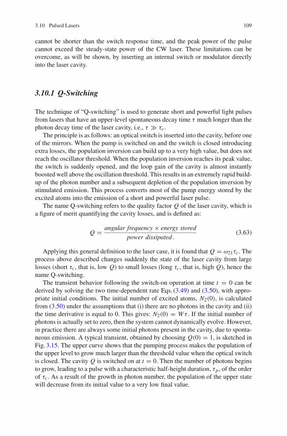
3.10 Pulsed Lasers 109
cannot be shorter than the switch response time, and the peak power of the pulsecannot exceed the steady-state power of the CW laser. These limitations can beovercome, as will be shown, by inserting an internal switch or modulator directlyinto the laser cavity.
3.10.1 Q-Switching
The technique of “Q-switching” is used to generate short and powerful light pulsesfrom lasers that have an upper-level spontaneous decay time τ much longer than thephoton decay time of the laser cavity, i.e., τ � τc.
The principle is as follows: an optical switch is inserted into the cavity, before oneof the mirrors. When the pump is switched on and the switch is closed introducingextra losses, the population inversion can build up to a very high value, but does notreach the oscillator threshold. When the population inversion reaches its peak value,the switch is suddenly opened, and the loop gain of the cavity is almost instantlyboosted well above the oscillation threshold. This results in an extremely rapid build-up of the photon number and a subsequent depletion of the population inversion bystimulated emission. This process converts most of the pump energy stored by theexcited atoms into the emission of a short and powerful laser pulse.
The name Q-switching refers to the quality factor Q of the laser cavity, which isa figure of merit quantifying the cavity losses, and is defined as:
Q = angular frequency × energy stored
power dissipated.(3.63)
Applying this general definition to the laser case, it is found that Q = ω21τc. Theprocess above described changes suddenly the state of the laser cavity from largelosses (short τc, that is, low Q) to small losses (long τc, that is, high Q), hence thename Q-switching.
The transient behavior following the switch-on operation at time t = 0 can bederived by solving the two time-dependent rate Eqs. (3.49) and (3.50), with appro-priate initial conditions. The initial number of excited atoms, N2(0), is calculatedfrom (3.50) under the assumptions that (i) there are no photons in the cavity and (ii)the time derivative is equal to 0. This gives: N2(0) = Wτ . If the initial number ofphotons is actually set to zero, then the system cannot dynamically evolve. However,in practice there are always some initial photons present in the cavity, due to sponta-neous emission. A typical transient, obtained by choosing Q(0) = 1, is sketched inFig. 3.15. The upper curve shows that the pumping process makes the population ofthe upper level to grow much larger than the threshold value when the optical switchis closed. The cavity Q is switched on at t = 0. Then the number of photons beginsto grow, leading to a pulse with a characteristic half-height duration, τp, of the orderof τc. As a result of the growth in photon number, the population of the upper statewill decrease from its initial value to a very low final value.

110 3 The Laser
Fig. 3.15 Time evolution of the population of the upper laser level (upper diagram) and of thelaser output power (lower diagram) in a Q-switched laser. The Q-switching operation is performedat t = 0
In order to derive the order of magnitude of the peak power, it can be assumedthat the total number of photons inside the pulse coincides with the total number ofexcited atoms at t = 0, V N2(0), leading to a peak output power estimate of:
Ppeak = hνV Wτ
τc. (3.64)
Recalling that the steady-state output power Ps is given by (3.55), and assuming,for simplicity, that W � Wth , the ratio of peak power to steady-state power in theemission is:
Ppeak
Ps= τ
τc. (3.65)
Equation (3.65) clearly shows that theQ-switching operation is only advantageousfor active media having a long spontaneous decay time of their excited levels, suchas solid-state and CO2 lasers. If one takes τ = 300µs and τc = 10ns for the caseof a Nd-YAG laser, then the power ratio can be up to 3 × 10⁴. A laser designed foran average output power of 1W can have a Q-switching pulse (sometimes called a“giant pulse” in the literature) with a peak power of 30kW.
The optical switch used inQ-switching can be realized exploiting the electro-opticor acousto-optic effects later described in Chap. 4. Another interesting possibility,
3.10 Pulsed Lasers 111
frequently utilized, is the inclusion of a saturable absorber in the optical cavityfor “passive” Q-switching. The absorber can be modeled as the two-level systemdescribed in Sect. 3.4, with an intensity-dependent absorption. The absorption lossis high in the early stages of the oscillation build-up, because the slowly increasingintensity is not large enough to saturate the absorption. However, once the intensityin the cavity exceeds a certain level (the saturation level, see (3.17)), the loss quicklydecreases, and the resulting effect is similar to that of a sudden opening of an opticalswitch.
3.10.2 Mode-Locking
Q-switching produces pulses with a duration ranging from a few nanoseconds tohundreds of nanoseconds. Another technique, known as “mode-locking”, is capableof producing pulses on the femtosecond and picosecond scale. Whereas Q-switchingcan work equally well with lasers in single-mode or multi-mode operation, mode-locking requires a large number of longitudinal modes in the cavity.
Consider a CW laser oscillating on N longitudinal modes. The frequency differ-ence between adjacent modes isΔν. For a Fabry-Perot cavity, Δν is given by (3.48).
The electric field associated to the laser beam is written as:
E(t) =N∑
k=1
Ekexp[−i(ωk t + φk)], (3.66)
where the amplitudes Ek are real and time-independent. The laser intensity, whichis proportional to |E(t)|2, is the sum of the intensities of the N modes plus the sumof N (N − 1) interference terms, each having zero time-average. If the phases φk arerandom and mutually uncorrelated, then the interference terms tend to cancel eachother, such that:
I (t) =N∑
k=1
Ik + ΔI (t), (3.67)
where ΔI (t) is a small randomly fluctuating term.The mode-locking operation consists in introducing a fixed relation among the
phases of different modes, expressed by:
φk − φk−1 = φo, (3.68)
where φo is an arbitrary constant. To simplify the algebra, it is assumed that N is anodd number and that the frequency of the central mode coincides with the centralfrequency ν21 of the gain band. Since N is odd, it can be written as: N = 2n + 1.

112 3 The Laser
By calling m the integer number that takes all values in the interval −n ≤ m ≤ n,assuming equal amplitudes, Em = Eo, and using (3.68), (3.66) then becomes:
E(t) =n∑
m=−n
Eoexp{−i[(ωo + mΔω)t + mφo]} = A(t)Eoexp(−iωot), (3.69)
where
A(t) =n∑
m=−n
exp[−im(Δωt + φo)]. (3.70)
It is convenient to introduce the new temporal variable t ′, connected to t by therelation Δωt + φo = Δωt ′. To use t ′ instead of t is equivalent to shifting the timeaxis by the quantity φo/Δω. The summation in the right-hand member of (3.70) is ageometric progression with common ratio exp(iΔωt ′). It is found:
A(t ′) =n∑
−n
exp(−imΔωt ′) = sin[(2n + 1)Δωt ′/2]sin(Δωt ′/2)
. (3.71)
The time-dependent intensity is derived from (3.71) by recalling that I (t ′) isproportional to Eo
2A2(t ′). As an example, the function I (t ′) is plotted in Fig. 3.16,for N = 11 and Δν = 100MHz. The intensity profile is a periodic sequence ofpulses, separated by a period of:
T = 2π
Δω= 1
Δν. (3.72)
Fig. 3.16 Temporal behavior of the output intensity of a mode-locked laser in the case of an equal-amplitude mode spectrum. In this numerical example 11 modes with a frequency separation of100MHz are considered

3.10 Pulsed Lasers 113
The peak intensity, Ip, is obtained by calculating A2(t ′) in the limit of t ′ tendingto 0. The result is:
Ip = N 2 Io = N IL , (3.73)
where Io is the intensity of one mode and IL = N Io is the average laser intensity.It is important to note that the pulsed behavior is the consequence of an inter-
ference effect, As such, mode-locking does not change the average power of theemission, it simply re-distributes the power non-uniformly in time. Therefore, theenergy contained in a single pulse must be equal to that of the integrated poweremitted by the CW laser over a period T . Consequently, the pulse duration τp canbe determined from the following equality:
τp Ip = T N IL τp = T
N. (3.74)
Recalling that T is the reciprocal ofΔν and that N = Δν21/Δν, the very importantresult is found that τp = (Δν21)
−1, regardless of the cavity length. As an example,the Nd-Y AG laser has a typical gain bandwidth of 200GHz, and so the minimumpulse duration that can be obtained from mode-locked operation is 5ps. For a Nd-glass laser, the bandwidth is one order-of-magnitude broader than that of a Nd-Y AGlaser, and so its minimum pulse duration is of the order of 500 fs. The pulse durationcan be reduced by another order of magnitude bymode-locking the Ti-sapphire laser.
The Fourier transform of the emitted field, E(ω), can be described as the productof an infinite comb of Dirac delta functions with a rectangle function:
E(ω) =∞∑
k→−∞Eorect
(2ω − ωo
Δω12
)δ(ω − ωk) (3.75)
where rect (x) is a function which takes value 1 if−0.5 ≤ x ≤ 0.5 and 0 if |x | > 0.5.Recalling that the inverse Fourier transform of the product of two functions of ω isthe convolution of the two anti-transforms, and that the Fourier anti-transform of rectis the sinc function, it can be verified that the anti-transform of (3.75) is preciselygiven by (3.69). The interesting aspect of this Fourier approach is that it allows fora general treatment to the more realistic case of unequal mode amplitudes. Indeedthe typical situation would be that in which the amplitudes of Ek are distributedaccording to a bell-shaped function, with maximum at k = 0. By using a Gaussiandistribution, E(ω) can be expressed as:
E(ω) =∞∑
k→−∞Eoexp
[(ωo − ωk)
2
Δω122
]δ(ω − ωk). (3.76)
It is apparent that the anti-transform of (3.76) gives an E(t) that consists in aperiodic sequence of Gaussian pulses, each having a duration inversely proportional

114 3 The Laser
to the bandwidth. It should be noted that the secondary maxima that are present in theintensity plot of Fig. 3.16 disappear when aGaussian distribution ofmode amplitudesis used instead of the rectangle function.
Mode-locking can be achieved in various ways. One method is to internally mod-ulate the losses of the laser at a frequency which is equal to the intermode frequencyspacing Δν. With this approach the laser behavior can be intuitively understood asa self-adjusting process: if losses are minimal at times to, to + T , etc., in order tomaximize the efficiency the laser will prefer to emit pulses at to, to + T , etc., insteadof operating at constant intensity. The loss modulation can be obtained by insertinginto the laser cavity an electro-optic or acousto-optic modulator.
The description of the N -mode laser as a collection of N independent oscillatorsis a rather rough approximation. In practice, even without any external intervention,the modes are interacting because they are driven by emission from the same activeatoms. Generally speaking, the existence of interactions among the modes tendsto favor the process of mode-locking. What prevents the laser from spontaneouslyoperating in a mode-locked regime is the fact that real longitudinal modes are notexactly equally spaced in frequency. The optical path appearing in (3.47) contains theindex of refraction of the activemedium,which is a frequency-dependent quantity.Asa consequence, (3.47) should be viewed as an implicit expression for the resonancefrequencies of the laser cavity, producing a spacing that is slightly different for eachpair of adjacent modes. Only if the modulation depth exceeds a threshold value, theamplitude (or phase) modulation forces the modes to become equally spaced andlocks the mode phases.
Mode-locking can also be achieved by passive methods. A frequently usedapproach is to insert a saturable absorber in the cavity. Initially, the multimode laserhas random intensity fluctuations, but the saturable absorber selectively transmitsthe fluctuations of high intensity, while absorbing those of low intensity. After manypasses through the cavity, only a single high-intensity pulse is formed. In this scheme,it is essential to use a saturable absorber with a recovery time much shorter than theperiod T . Semiconductor saturable-absorber mirrors (SESAMs) can also providepassive mode-locking. Furthermore, as it will be explained in Chap. 7, spontaneousmode-locking can be achieved in solid-state lasers by exploiting the nonlinear opticalbehavior of the active medium. This method is called Kerr-lens mode locking.
Ultrashort pulses of high peak power can be obtained by simultaneously operat-ing in the same laser cavity mode-locking and Q-switching. In such a situation theobtained mode-locked train has an envelope that follows the time evolution of theQ-switching pulse. As an example, Fig. 3.17 illustrates the result of an experimentin which a passively mode-locked diode-pumped Nd-Y V O4 laser is Q-switchedby an acousto-optic switch. The output train is made up of about 20 mode-lockedpulses, separated by a period of 5.6ns corresponding to the cavity round trip time.The measured width of the pulses was about 9ps.

3.11 Properties of Laser Light 115
Fig. 3.17 Output intensity of a simultaneously mode-locked and Q-switched Nd-Y V O4 laser
3.11 Properties of Laser Light
Laser light differs from the light emitted by conventional sources in many aspects.The most relevant properties of laser emission are reviewed below.
3.11.1 Directionality
Laser radiation is characterized by a high degree of directionality. While traditionallight sources emit in all directions and with a wide frequency range, the laser (as anoscillator) has a built-in selection mechanism for frequency and direction. The originof the directionality can be intuitively understood, if one considers that only raystraveling back-and forth between the cavitymirrors, along the cavity axis, are stronglyamplified by the active medium. As discussed in Sect. 3.8, the spatial properties oflaser beams can be described in terms of Gaussian waves. If the cavity supportsseveral transverse modes, then the fundamental mode TEM00, can be selected byplacing an aperture within the cavity. The TEM00 laser emission has an angularspread θo typically in the range 10−4 − 10−3 radians.
The beam can be further collimated by a telescope consisting of a pair of twoconverging lenses sharing a common focus. If the focal length of the first lens isf1 and that of the second lens is f2 > f1, then the beam diameter is increased bythe factor f2/ f1, and, consequently, the beam divergence is decreased by the samefactor.

116 3 The Laser
In many applications, such as writing and reading optical memories, a laser beamis focused to a very small spot size. Using a lens with focal length f , the spot sizein the focal plane is approximated by w f ≈ θo f . Taking θo = 10−4 and f = 1cm,it is found that w f = 1µm. This shows that the small divergence of a laser beamenables the concentration of the output power to an area having the size of the opticalwavelength. This is useful for many applications. In the case of materials processing,the intensity at focus can be easily large enough to strongly heat the material, andlocally produce melting or even vaporization.
3.11.2 Monochromaticity
There are applications, such as optical communications, in which it is essential tohave a single-frequency optical source. This requires suppression not only of higher-order transverse modes, but also of all-but-one longitudinal modes. In almost allcases, the bandwidth of the frequency-dependent gain profile Δν21 is much largerthan the frequency spacing between adjacent longitudinalmodes,Δν, and so the laserhas a natural tendency to operate with multiple modes. Single-mode behavior canbe enforced by using compound cavities or, more effectively, by using a frequency-selective feedbackmechanism. An example of this approach will be given in Chap.5,where single-mode semiconductor lasers will be discussed.
The emission frequency of a single-mode laser, νL , always has fluctuations orig-inated by external disturbances. Since νL is linearly dependent on the optical pathL ′ between the two laser mirrors, the frequency stability of the laser depends onthe stability of L ′. As shown in Sect. 2.4.4, to shift by Δν the mode frequency, it issufficient to change the mirror separation by half wavelength. This means that smallvariations in the mirror separation can induce large changes of the laser emissionwavelength. Therefore, in order tominimize thewavelengthfluctuations of the single-mode laser, the cavity length must be kept fixed by rigid construction, with isolationfrom mechanical vibrations, and also with temperature control. In a stable single-mode laser the linewidth δνL of the emitted radiation can be of the order of 1MHz,and even lower values of 1kHz can be achieved using active frequency-stabilizationmethods.
A useful feature of some types of lasers is the possibility to tune the emissionwavelength without changing the active medium, but simply acting on an opticalcomponent inside the cavity.
It should be noted that, in principle at least, one can filter both the direction andfrequency of light emitted by a conventional source, in order to achieve a divergenceand bandwidth comparable to a laser source. However, the resulting beam wouldbe not only extremely weak, but also characterized by large amplitude and phasefluctuations.

3.11 Properties of Laser Light 117
3.11.3 Spectrum of Laser Pulses
The light emitted by conventional optical sources contains many frequency com-ponents. Each component has a random phase, uncorrelated with that of the othercomponents. In the laser case, it is possible to have a multi-frequency emission inwhich the phases of different frequency components are mutually correlated, as it hasbeen shown in Sect. 3.10.2. This is very important because it allows for the possibil-ity of optical signals having a pre-determined time-dependent (and space-dependent)amplitude and phase, analogous towhat can be done in the range of radio-frequenciesor microwaves with an electronic function generator.
In this section the relation between pulse duration and spectral width is derivedby considering a specific pulse shape, that of the time-dependent field amplitudedescribed by a Gaussian function. Assuming that the intensity peak is at t = 0, theelectric field can be expressed as:
E(t) = Aoexp
(− t2
2τi2
)exp(−iωot), (3.77)
where ωo is the central frequency, and τi is the time delay at which the intensity isreduced by a factor 1/e with respect to the peak value. The pulse duration τp, definedas the width at half-height of the intensity peak, is related to τi as follows:
τp = 2√
ln2τi = 1.67τi . (3.78)
Recalling the definite integral:
∫ ∞
0exp(−a2t2)dt =
√π
2a, (3.79)
the Fourier transform of (3.77) can be immediately calculated, obtaining:
E(ω) = √2πτi Ao exp
(− τi
2(ω − ωo)2
2
). (3.80)
Note that E(ω) is a real function, which means that all the frequency componentshave the same phase. This type of optical pulse is known as a “transform-limited”pulse. Equation (3.80) shows that the power spectrumof theGaussian pulse, Sp(ω) ∝|E(ω)|2, is also a Gaussian function. The Gaussian pulse, together with its powerspectrum, is illustrated in Fig. 3.18. The width at half-height of the power spectrum,Δνp, satisfies the relation:
Δνpτp = 2 ln2
π= 0.441. (3.81)

118 3 The Laser
Fig. 3.18 The Gaussian pulse and its power spectrum
It is a general property of transform-limited light pulses that the bandwidth-duration product is a number of the order of 1. The precise value of the productdepends on the shape of the pulse. In the more general case of pulses which arenot transform-limited, (3.81) gives only the lower bound of the bandwidth-durationproduct. To consider an extreme situation, a short pulse of solar light can be createdby using a fast switch on a Sun beam. This pulse would have the spectrum of Sunlight, regardless of its duration, so that the bandwidth-duration product would belarger than 0.441 by many orders of magnitude.
Problems
3.1 What is the momentum of a 1018-Hz X-ray photon?
3.2 If 0.5% of the light intensity incident into a medium is absorbed per millimeter,what fraction is transmitted if the medium is 10cm long? Calculate the absorptioncoefficient α.
3.3 Calculate the photon decay time τc for a ring laser cavity having length 30cmand mirror reflectances R1 = 0.95 and R2 = 0.85.
3.4 An Nd-YAG laser having a Fabry-Perot cavity of length 30cm and an activemedium of length 5cm is operated in the mode-locking regime. Assuming that theindex of refraction of the active medium is n = 2 and that the gain bandwidth is200GHz, calculate the repetition period T and the duration τp of the emitted pulses.
3.5 Considering that the gain bandwidth of a He-Ne laser is 1.5GHz, which is themaximumFabry-Perot cavity length that ensures single longitudinalmode operation?
3.6 Calculate the mirror reflectance required to sustain oscillation in a symmetricFabry-Perot laser cavity, assuming that the active medium has a small-signal gaincoefficient of 1m−1 and is 0.1m long.

Problems 119
3.7 Consider a Fabry-Perot cavity Nd-YAG laser, in which the Nd-YAG crystal haslength L = 2cm and mirror 1 is totally reflecting. Assuming that the populationinversion inside the active medium is N2 − N1 = 1 × 1018 cm−3, the stimulatedemission cross-section is σ21 = 3.5 × 10⁻¹⁹ cm2, the loop gain is equal to 2, deter-mine the reflectance of mirror 2.

Chapter 4Modulators
Abstract The application of an external field can modify the optical properties of amaterial. By controlling the strength and frequency of the external field, the ampli-tude, phase, or polarization of the optical beam can be controlled and modulated.The most important modulation methods are those using electric fields, but bothacoustic fields and magnetic fields can be exploited. This chapter describes linearand quadratic electro-optic effects, and explains the most common modulation andswitching schemes. Modulation methods based on liquid crystals are also brieflydiscussed. The final part of the chapter is devoted to the acousto-optic effect and itsapplications to amplitude modulation and to beam deflection.
4.1 Linear Electro-Optic Effect
The electro-optic effect is the change in the index of refraction due to an appliedelectric field. If the refractive index change is proportional to the applied field, thenthe effect is known as Pockels effect. If the index change is quadratically-dependenton the applied field, then the effect is known as Kerr effect. As it will be seen, thePockels effect can exist only in crystalline materials, and is absent in amorphousmaterials, such as glasses and fluids. In contrast, the Kerr effect is present in allclasses of materials.
In general, crystals are anisotropic media, in which D and P are related to the fieldE by a second-rank tensor, as was seen in Chap.2. In particular:
Pi(ω) = εo
3∑
j=1
χijEj(ω), (4.1)
where the indices i, j can take the values 1, 2, 3. As usual, 1 = x, 2 = y, 3 = z. Theelectric susceptibility tensor χij is connected to εij by the relations εii = 1+χii, and,for i �= j, εij = χij. The two tensors have the same diagonal system of coordinates.
The electro-optic effect modifies the relation between P and E, by introducingadditional terms dependent on an external field E′. In the case of the Pockels effect,the additional terms are linear with respect to the external field components:
© Springer International Publishing Switzerland 2016V. Degiorgio and I. Cristiani, Photonics, Undergraduate Lecture Notes in Physics,DOI 10.1007/978-3-319-20627-1_4
121

122 4 Modulators
Pi(ω) = εo
3∑
j,k=1
(χij + χijkE′k)Ej(ω). (4.2)
Equation (4.2) is nonlinear because it contains terms proportional to the productof two electric fields. A general description of nonlinear interactions will be given inChap.7. In the case under discussion here, it is important to keep in mind that E isthe electric field associated with an optical wave, while E′ is a field generated by anelectronic device. Thus the oscillation frequency of E is several orders of magnitudelarger than that of E′. The external field acts as a parameter modifying the electricsusceptibility of the medium, and, consequently, its refractive index.
In a centrosymmetric medium all the components of χijk vanish. In fact, thepresence of non-zero components would induce the existence of terms cubic inthe electric field inside the electromagnetic energy density. Cubic terms change signwhen the variable changes sign, but, in a centrosymmetricmedium, the energy densitycannot depend on the sign of the electric field.
The tensor χijk has 33 = 27 components, but, since it is symmetric with respectto the exchange of i with j, only 18 components are independent. For all crystalclasses, symmetry considerations can be used to predict which components of χijkare independent and non-zero.
In the scientific literature the name electro-optic tensor designs rijk , which isconnected to χijk by the relation:
χijk = −(1 + χii)(1 + χjj)rijk (4.3)
A single index n can be introduced to replace the ij pair, using the following con-vention: n = 1, 2, 3, 4, 5, 6 corresponds to ij = 11, 22, 33, 23, 13, 12, respectively.For instance, in this contracted notation, r123 becomes r63 and r333 becomes r33. Thevalues of the refractive indices and of the non-zero electro-optic coefficients of sometypical crystals are reported in Table4.1.
Table 4.1 Properties of some electro-optic crystals at λ = 633nm
Crystal Class Indices of refraction r (10−12 m/V)
LiNbO3 3m no = 2.272, ne = 2.187 r33 = 30.8, r13 = 8.6
r22 = 3.4, r51 = 28
KNbO3 mm2 n1 = 2.279, n2 = 2.329 r33 = 25, r13 = 10
n3 = 2.167
LiTaO3 3m no = 2.175, ne = 2.180 r33 = 33, r13 = 8
KDP 42m no = 1.51, ne = 1.47 r41 = r52 = 8.6, r63 = 10.6
ADP 42m no = 1.52, ne = 1.48 r41 = r52 = 28, r63 = 8.5
Lithium niobate (LiNbO3), potassium niobate (KNbO3), lithium tantalate (LiTaO3), potassium di-hydrogenated phosphate (KH2PO4, usually designed as KDP), ammonium di-hydrogenated phos-phate (NH4H2PO4, usually designed as ADP)

4.1 Linear Electro-Optic Effect 123
Crystals that have a symmetry supporting the Pockels effect also exhibit piezo-electric effects. This means that they expand and contract under the application ofan external electric field. Piezoelectric effects are usually negligible for frequenciesof the applied field larger than some MHz.
Up to frequencies of the order of 1THz, the induced polarization contains contri-butions from the displacements of both ions and electrons. Above 1THz, there areonly electronic contributions and coefficients are proportionally smaller. The valuesreported in Table4.1 refer to the frequency range between 1 MHz and 1THz.
From a general point of view the wave propagation inside the electro-optic crystalshould be treated by inserting (4.2) into the wave equation (2.7). Since, as it has beenseen in Chap.2, the propagation characteristics are fully described by means of theindex ellipsoid, the effect of the electric field is expressed most conveniently in termsof changes of the index ellipsoid. In presence of E′, (2.126) is modified as follows:
( 1
n21+ a1
)x2 +
( 1
n22+ a2
)y2 +
( 1
n23+ a3
)z2
+ 2a4yz + 2a5xz + 2a6xy = 1,
(4.4)
where the coefficients an are given by:
an =3∑
k=1
rnkE′k (4.5)
As an example, considering KDP, which has only three non-zero components ofrnk , (4.4) becomes:
x2 + y2
n2o+ z2
n2e+ 2r41E′
1yz + 2r52E′2xz + 2r63E′
3yz = 1 (4.6)
The effect of the additional terms is that ofmodifying the direction of the dielectricaxes and the length of the semi-axes. The modulator configurations described in thefollowing sections will deal with rather simple situations in which E′ is directedalong the optical axis z and the light beam propagates along a principal axis.
4.1.1 Phase Modulation
The phase of an optical wave can be electro-optically modulated. For this type ofapplication, the optical wave is linearly polarized in a direction that is parallel toone of the principal axes of the crystal in presence of the external field, so thatits polarization state does not change during propagation. In order to illustrate themethod two specific situations are below discussed in some detail.

124 4 Modulators
Modulation based on r33. Lithium niobate is a crystal often used in electro-opticmodulation. It has a high electro-optic coefficient r33, as shown in Table4.1. Theconfiguration adopted to access the r33 term is having the light beam traveling alongx, linearly polarized along the optical axis z (extraordinary wave), and the externalelectric field E′ parallel to z. In this configuration the extraordinary wave propagateswithout changing its state of polarization, whether E′ is present or not. Using (4.2),it is found that the only non-zero component of P is that which lies along z:
P3 = εo(χ33 + χ333E′3)E3 = εo(χ33 − n4er33E′
3)E3 (4.7)
Equation (4.7) indicates that the extraordinary indexof refraction,ne = √1 + χ33,
is modified by the presence of E′, and becomes:
n′e =
√1 + χ33 − n4er33E′
3 = √1 + χ33
√
1 − n4er33E′3
1 + χ33
≈ ne − r33ne3E′
3
2,
(4.8)
where, taking into account that n4er33E′3 is usually much smaller than 1 + χ33, the
approximate expression is obtained by a truncated series expansion of the squareroot term.
Calling L the crystal length, the phase delay caused by the Pockels effect is givenby:
Δφ = 2π(n′e − ne)
L
λ= −2π
r33n3eE′3
2
L
λ. (4.9)
If L is a few centimeters and λ is around 1µm, then the ratio of L/λ is of the orderof 104. This means that a refractive index variation of just 10−4 can give a phasedelay Δφ of the order of π radians.
A phase modulator can be realized by using a lithium niobate crystal cut asa parallelepiped along the principal axes. A voltage difference V across the crystalthickness d induces an electric field E′ = V/d directed along z. The wave propagateswithout changing polarization, and acquires a phase delayΔφ. Taking Eocos(ωot) asthe electric field of the incident wave, and assuming, for simplicity, that the appliedvoltage oscillates with an angular frequency ωm, such that V(t) = Vosin(ωmt), theelectric field of the wave that travels for a length L inside the crystal is:
E(t) = Eocos{ωot − 2π
λ
[ne − r33n3e
2dVosin(ωmt)
]L}. (4.10)
Equation (4.10) describes a wave at frequency ωo, phase modulated at the fre-quency ωm.
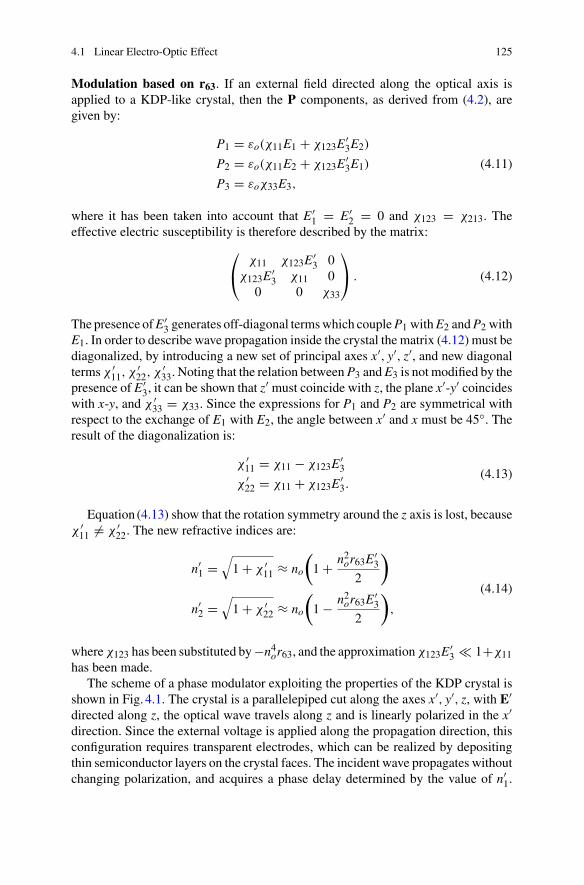
4.1 Linear Electro-Optic Effect 125
Modulation based on r63. If an external field directed along the optical axis isapplied to a KDP-like crystal, then the P components, as derived from (4.2), aregiven by:
P1 = εo(χ11E1 + χ123E′3E2)
P2 = εo(χ11E2 + χ123E′3E1)
P3 = εoχ33E3,
(4.11)
where it has been taken into account that E′1 = E′
2 = 0 and χ123 = χ213. Theeffective electric susceptibility is therefore described by the matrix:
⎛
⎝χ11 χ123E′
3 0χ123E′
3 χ11 00 0 χ33
⎞
⎠ . (4.12)
The presence ofE′3 generates off-diagonal termswhich coupleP1 withE2 andP2 with
E1. In order to describe wave propagation inside the crystal the matrix (4.12) must bediagonalized, by introducing a new set of principal axes x′, y′, z′, and new diagonalterms χ ′
11, χ′22, χ
′33. Noting that the relation betweenP3 andE3 is not modified by the
presence of E′3, it can be shown that z′ must coincide with z, the plane x′-y′ coincides
with x-y, and χ ′33 = χ33. Since the expressions for P1 and P2 are symmetrical with
respect to the exchange of E1 with E2, the angle between x′ and x must be 45◦. Theresult of the diagonalization is:
χ ′11 = χ11 − χ123E′
3
χ ′22 = χ11 + χ123E′
3.(4.13)
Equation (4.13) show that the rotation symmetry around the z axis is lost, becauseχ ′11 �= χ ′
22. The new refractive indices are:
n′1 =
√1 + χ ′
11 ≈ no
(1 + n2or63E′
3
2
)
n′2 =
√1 + χ ′
22 ≈ no
(1 − n2or63E′
3
2
),
(4.14)
whereχ123 has been substituted by−n4or63, and the approximationχ123E′3 � 1+χ11
has been made.The scheme of a phase modulator exploiting the properties of the KDP crystal is
shown in Fig. 4.1. The crystal is a parallelepiped cut along the axes x′, y′, z, with E′directed along z, the optical wave travels along z and is linearly polarized in the x′direction. Since the external voltage is applied along the propagation direction, thisconfiguration requires transparent electrodes, which can be realized by depositingthin semiconductor layers on the crystal faces. The incident wave propagates withoutchanging polarization, and acquires a phase delay determined by the value of n′
1.
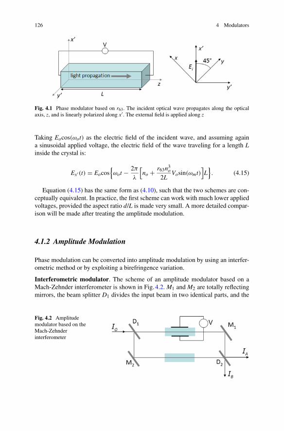
126 4 Modulators
Fig. 4.1 Phase modulator based on r63. The incident optical wave propagates along the opticalaxis, z, and is linearly polarized along x′. The external field is applied along z
Taking Eocos(ωot) as the electric field of the incident wave, and assuming againa sinusoidal applied voltage, the electric field of the wave traveling for a length Linside the crystal is:
Ex′(t) = Eocos{ωot − 2π
λ
[no + r63n3o
2LVosin(ωmt)
]L}. (4.15)
Equation (4.15) has the same form as (4.10), such that the two schemes are con-ceptually equivalent. In practice, the first scheme can work with much lower appliedvoltages, provided the aspect ratio d/L is made very small. A more detailed compar-ison will be made after treating the amplitude modulation.
4.1.2 Amplitude Modulation
Phase modulation can be converted into amplitude modulation by using an interfer-ometric method or by exploiting a birefringence variation.
Interferometric modulator. The scheme of an amplitude modulator based on aMach-Zehnder interferometer is shown in Fig. 4.2. M1 and M2 are totally reflectingmirrors, the beam splitter D1 divides the input beam in two identical parts, and the
Fig. 4.2 Amplitudemodulator based on theMach-Zehnderinterferometer

4.1 Linear Electro-Optic Effect 127
beam splitterD2 recombines the two beams at the two outputs A and B. Two identicallithium niobate crystals are inserted in the upper and lower branches of the interfer-ometer. The optical beams propagate through the crystals in a direction perpendicularto the optical axis and are linearly polarized along the optical axis. Qualitatively thebehavior is as follows. If the upper and lower optical paths are identical, then thereis constructive interference at output A and destructive interference at output B. Ifall the components are lossless, then the optical intensity at A, IA, coincides with theinput intensity, Io, and IB is zero. By applying an electric field to the upper crystal,the index of refraction is changed, such that the wave traveling in the upper branchwill acquire an additional phase delay. As a consequence, the interferometer will beunbalanced, and some part of the input intensity will appear at output B.
The electric field of the wave at the output A (or B), EA (EB), is the sum of thecontributions coming from the upper and lower branch of the interferometer. TakingEocos(ωot) as the electric field of the incident wave, and considering all the phasedelays experienced by the beams propagating in the upper and lower branch of theinterferometer, the electric fields EA and EB of the two output beams are expressedas:
EA = Eo
2[cos(ωot − φ1) + cos(ωot − φ2)]
EB = Eo
2[cos(ωot − φ3) + cos(ωot − φ4)]
(4.16)
Calling φτ and φρ the phase delays in transmission and reflection due to the beamsplitters D1 and D2, and φM the phase delay due to reflection at M1 and M2, the phasedelays of (4.16) are expressed as:
φ1 = φτ + 2πLup/λ + φρ + φM
φ2 = φρ + 2πLdown/λ + φτ + φM
φ3 = φτ + 2πLup/λ + φτ + φM
φ4 = φρ + 2πLdown/λ + φρ + φM .
(4.17)
The upper and lower optical paths are given by:Lup = n′eL+Lo,Ldown = neL+Lo,
respectively, where L is the length of the two crystals and Lo is the path in air. Takinginto account that φτ and φρ are related by (2.58), it is found that: φ1 − φ2 = Δφ,and φ3 − φ4 = Δφ − π . Δφ is the phase delay caused by the Pockels effect, and isgiven by (4.9).
The intensity IA(IB) at output A(B) is proportional to the square of EA(EB). Recall-ing that:
cosα + cosβ = 2cos
(α + β
2
)cos
(α − β
2
)
it is found that:
IA = Iocos2(φ1 − φ2
2
)= Iocos
2(Δφ
2
), (4.18)

128 4 Modulators
and
IB = Iocos2(φ3 − φ4
2
)= Iosin
2(Δφ
2
). (4.19)
Equations (4.18) and (4.19) show that, ifΔφ = ±π , then thewhole input intensityis transferred to output B. The applied voltage needed for a phase shift of π , knownas the half-wave voltage, is given by:
Vπ = λd
r33Lne3 . (4.20)
Since the transmittance of the Mach-Zehnder interferometer, observed at out-put B, ranges from 0 to 1 when the applied voltage is changed from 0 to Vπ , theinterferometer can be used as an electro-optic switch.
If the applied voltage is a continuously varying signal, for instance the sinusoidalfunction V(t) = Vmsin(ωmt), then the device behaves as an amplitude modulator.However, the output intensity is not linearly dependent on the applied voltage. In orderto obtain a linear relation, at least in the small signal regime, theworking region shouldbe shifted around the inflexion point of the curve IB/Io versus V , as shown in Fig. 4.3.This can be achieved by adding a DC bias voltage Vπ/2 = Vπ/2, which introduces afixed phase shift π/2. The total applied voltage becomes: V = Vπ/2 + Vmsin(ωmt).By using (4.19), the ratio IB/Io takes the expression:
IB
Io= sin2
[π
4+ πVmsin(ωmt)
2Vπ
]. (4.21)
Fig. 4.3 Analog modulation based on the Mach-Zehnder interferometer

4.1 Linear Electro-Optic Effect 129
Fig. 4.4 Equivalent electriccircuit of the crystal withapplied voltage
If Vm/Vπ � 1, (4.21) can be approximated as:
IB
Io= 1
2
{1 + 2sin
[πVmsin(ωmt)
2Vπ
]}≈ 1
2
[1 + πVmsin(ωmt)
Vπ
], (4.22)
obtaining a linear relation between applied voltage and output intensity. The ampli-tude modulation used in optical communications operates around the inflexion pointof the curve IB versus V .
The intrinsic response time of the Pockels effect can be smaller than 10−11 s. Thelimits to the speed of the device come from electrical capacitive effects: the crystalbehaves as a capacitor with capacity C, charged by a voltage generator with internalresistance Rs (see Fig. 4.4). Therefore, if the modulation frequency ωm is larger than(RsC)−1, thenmost of the applied voltage will be dropped across Rs instead of acrossthe crystal. Considering the problem in the time domain, the response time is givenby RsC. Recalling that C = εoεrA/d, where A is the surface area, a quick calculationshows that the typical response time is of the order of 1 ns.
A method to reduce the response time is to put a coil with inductance Lo and aresistor Ro in parallel to the crystal, such that ωm
2 = (LoC)−1 and Ro � Rs. Atresonance, the impedance of the parallel RoLoC is equal to Ro, and so the appliedvoltage is dropped almost completely across the crystal. The price to pay in thisconfiguration is that the device can operate only in a band of modulation frequenciescentered at ωm with a width Δω = (RoC)−1.
The modulation induced by the applied field is effective only if the transit timeof the optical wave through the crystal is smaller than the modulation period Tm =2π/ωm. Indeed, instead of using (4.9), Δφ should be more generally calculated as:
Δφ = −2πr33ne3
2λ
∫ L
0E′3dz = −ωr33ne
2
2
∫ t+τd
tE′3(t
′)dt′, (4.23)
where τd = Lne/c is the transit time through the crystal, and E′3(t
′) is the instan-taneously applied field. In the right-hand member of (4.23), the spatial integra-tion has been substituted by a temporal integration by putting dt′ = nedz/c. IfE′3 = E′
osin(ωmt), Δφ is given by:
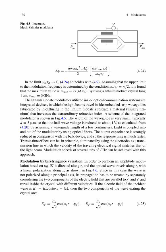
130 4 Modulators
Fig. 4.5 IntegratedMach-Zehnder modulator
Δφ = −ωr33ne2τdE′
o
2
[sin(ωmτd)
ωmτd
]. (4.24)
In the limit ωmτd → 0, (4.24) coincides with (4.9). Assuming that the upper limitto the modulation frequency is determined by the condition ωmτd = π/2, it is foundthat the maximum value is: νmax = c/(4Lne). By using a lithium niobate crystal long1cm, νmax = 3GHz.
The lithiumniobatemodulators utilized inside optical communication systems areintegrated devices, in which the light beams travel inside embedded strip waveguidesfabricated by in-diffusing in the lithium niobate substrate a material (usually tita-nium) that increases the extraordinary refractive index. A scheme of the integratedmodulator is shown in Fig. 4.5. The width of the waveguide is very small, typicallyd = 5 µm, so that the half-wave voltage is reduced to about 1V, as calculated from(4.20) by assuming a waveguide length of a few centimeters. Light is coupled intoand out of the modulator by using optical fibers. The output capacitance is stronglyreduced in comparison with the bulk device, and so the response time is much faster.Transit-time effects can be, in principle, eliminated by using the electrodes as a trans-mission line in which the velocity of the traveling electrical signal matches that ofthe light beam. Modulation speeds of several tens of GHz can be achieved with thisapproach.
Modulation by birefringence variation. In order to perform an amplitude modu-lation based on r63, E′ is directed along z, and the optical wave travels along z, witha linear polarization along x, as shown in Fig. 4.6. Since in this case the wave isnot polarized along a principal axis, its propagation has to be treated by separatelyconsidering the two components of the electric field that are parallel to x′ and y′ andtravel inside the crystal with different velocities. If the electric field of the incidentwave is Ex = Eocos(ωot − kz), then the two components of the wave exiting thecrystal are:
Ex′ = Eo√2cos(ωot − φx′) ; Ey′ = Eo√
2cos(ωot − φy′). (4.25)

4.1 Linear Electro-Optic Effect 131
Fig. 4.6 Amplitude modulator based on r63. The input wave is linearly polarized along x. The axisof the output polarizer is along y
The relative phase delay is:
Δφ = φx′ − φy′ = 2πn3or63V
λ, (4.26)
where V = LE′3 is the applied voltage. The output wave is elliptically polarized,
that is, a modulation of the polarization is produced. In order to transform the deviceinto an amplitude modulator, it is sufficient to add a polarizer with the optical axisparallel to y, as shown in Fig. 4.6. The electric field of the wave transmitted by thepolarizer is the sum of the projections of Ex′ and Ey′ on the y axis:
Ey = (Eo/2)[cos(ωot − φy′) − cos(ωot − φx′)]= Eosin(ωot − φo)sin(Δφ/2),
(4.27)
where φo = (φx′ + φy′)/2. The ratio between output and input intensity is:
Iu
Io= sin2
(Δφ
2
)= sin2
( πV
2Vπ
), (4.28)
where
Vπ = λ
2r63n3o(4.29)
is the half-wave voltage for this configuration.Equation (4.28) is identical to (4.19), therefore the two amplitude modulators are
equivalent in principle. However, by comparing (4.29) with (4.20), a very importantdifference appears: if the electric field E′ is applied transversally to the directionof wave propagation, then Vπ becomes proportional to the aspect ratio d/L. As aconsequence, if a small aspect ratio is used for the transverse modulation, as in thecase of the integrated modulator of Fig. 4.5, then Vπ can be of the order of 1V. Incontrast, the longitudinal modulation scheme of Fig. 4.6, taking also into account that

132 4 Modulators
the electro-optic coefficient of KDP is much smaller than that of lithium niobate, hasa half-wave voltage of several kilovolts.
It is instructive to discuss the amplitude modulator of Fig. 4.6 by using the for-malism of Jones matrices described in Sect. 2.5.2. Defining Vo as the Jones vector ofthe input wave, Vu the vector of the output wave, T1, T2, T3, the matrices describingthe input polarizer, the electro-optic crystal, and the output polarizer, respectively,then Vu is given by:
Vu = T3T2T1Vo(0 00 1
) ((exp(−iΔφ) + 1
)/2
(exp(−iΔφ) − 1
)/2(
exp(−iΔφ) − 1)/2
(exp(−iΔφ) + 1
)/2
) (1 00 0
) (10
)
=(
0[exp(−iΔφ) − 1
]/2
).
(4.30)
The ratio between output and input intensity is simply given by:
Iu
Io=
∣∣∣∣exp(−iΔφ) − 1
2
∣∣∣∣
2
= 1 − cos(Δφ)
2= sin2
(Δφ
2
), (4.31)
which coincides with (4.28).In order to operate the modulator in a linear region, a quarter-wave plate, having
x′ and y′ as principal axes, can be inserted after the crystal. Using the x and y axesas the reference system, the matrix describing the plate is:
T′2 =
((exp(−iπ/2) + 1
)/2
(exp(−iπ/2) − 1
)/2(
exp(−iπ/2) − 1)/2
(exp(−iπ/2) + 1
)/2
). (4.32)
The output signal becomes:
Vu = T3T′2T2T1Vi =
(0(
exp(−i(Δφ + π/2) − 1)/2
), (4.33)
and the ratio Iu/Io is given by:
Iu
Io= 1 − cos(Δφ + π/2)
2= sin2
(Δφ
2+ π
4
). (4.34)
The insertion of the quarter-wave plate has the effect of shifting the operatingpoint of the modulator to the inflexion point of the curve Iu/Io versus V . Note that inthe case of the interferometric amplitudemodulator described in the previous section,the same effect was obtained by applying a bias voltage equal to Vπ/2 (see Fig. 4.3).
A transverse modulation scheme could also be applied to the KDP modulator, asshown in Fig. 4.7, where E′ is parallel to z, and the light beam propagates in the y′direction, with a linear polarization at 45◦ with z. The phase delay Δφ between thex′ and z components is given by:

4.1 Linear Electro-Optic Effect 133
Fig. 4.7 Amplitude modulator based on r63 in a transverse scheme. The external electric field isapplied along z and the light beam propagates along y′
Δφ = φx′ − φz = 2πL
λ
(no − ne + n3or63V
2d
), (4.35)
where d is the crystal thickness. Equation (4.35) shows that Δφ is non-zero even inabsence of E′. This is obvious, because the light beam is not propagating along theoptical axis. However, the presence of the voltage-independent term complicates theutilization of the transverse configuration.
The electro-optic methods described in this section are also utilized for the gen-eration of ultrashort laser pulses. In the case of a Q-switched laser, a fast opticalswitch can be realized by inserting into the cavity an electro-optic shutter that blocksthe laser beam when voltage is applied to the crystal and is suddenly opened byremoving the voltage. Electro-optic modulators can be used to drive a laser in themode-locking regime by intra-cavity modulation at a frequency ωm ≈ 2πΔν, whereΔν is the frequency difference between two adjacent longitudinal modes of the lasercavity.
4.2 Quadratic Electro-Optic Effect
Centrosymmetric materials may exhibit a quadratic electro-optic effect, i.e. a refrac-tive index change proportional to the square of the applied electric field:
Δn = nK E′2, (4.36)
where nK , measured in m2/V2, is the Kerr constant. It should be mentioned thatmany authors define differently the Kerr constant, by writing Δn = λn′
K E′2,where λ is the wavelength of the modulated light beam and the constant n′
K is mea-sured in m/V2.

134 4 Modulators
In general terms, the relation between P and E takes the following form:
Pi = εo
⎛
⎝∑
j
χijEj +∑
j,k,l
χijklE′kE′
lEj
⎞
⎠ (4.37)
The tensor χijkl has 34 = 81 components. In an isotropic material, only thecomponents of the type χiiii or χiikk are non-zero.
Because of the Kerr effect, an isotropic material becomes uniaxial, taking thedirection of the applied electric field as the optical axis. Assume that χ is the electricsusceptibility and n = √
1 + χ the refractive index of the isotropic material, and thatE′ is parallel to z. For a wave traveling along y and linearly polarized along z theextraordinary index of refraction is:
ne = n + neK E′2 (4.38)
where ne2 is proportional to the component χ3333. For the wave traveling along y, but
polarized along x, the ordinary refractive index is:
no = n + noK E′2, (4.39)
where no2 is proportional to χ1133. Therefore the two Kerr constants are generally
different.In solid media the Kerr effect is mainly connected with a displacement of electron
clouds,whereas influidmedia important contributionsmaycome from theorientationof anisotropic molecules. The electro-optic effects of electronic origin are usuallysmall, but have very short response times. In contrast, orientational Kerr effects canbe large, but have correspondingly long response times.
In absence of an applied field a liquid consisting of elongated molecules behavesas an isotropic medium because the molecular orientations are completely random.When an electric field is applied, the molecules tend to orient parallel to each other,and the medium becomes uniaxial. If E′ is not very large, then the first-order theorypredicts that the change in refractive index is proportional to E′2, and that no
K =−ne
K/2. For large E′, the molecules become all parallel to the field, and the mediumbirefringence attains a saturation value.
In principle the Kerr effect can be utilized for electro-optic modulation by usingschemes similar to those of Pockels modulators. In practice, the most importantapplications involve liquid crystals, and are discussed in the next section.
A very interesting aspect of the Kerr effect is that, being quadratic, it can also beeffective when the applied field is oscillating at very large frequencies, such as theoptical frequencies. This is known as the optical Kerr effect, and will be discussedin Chap.7.

4.2 Quadratic Electro-Optic Effect 135
4.2.1 Liquid Crystal Modulators
A particularly large quadratic electro-optic effect is shown by liquid crystals, withvery important applications in displays or in other situations not requiring fastresponse times. In normal cases a solid material, when heated to its melting point,becomes a liquid, and undergoes a phase transition from an ordered state to a dis-ordered state. Liquid crystals are a particular class of materials that present one (ormore) intermediate states between the crystalline solid and the isotropic liquid. Theyare fluid-like, yet the arrangement of molecules exhibits structural order. A charac-teristic of liquid crystals is the rod-like shape of their molecules. Within the liquidcrystal family, there are three distinct molecular structures: nematic, cholesteric,and smectic, as shown in Fig. 4.8. Only the first two structures are of importance inmodulators and displays. In the nematic phase, the elongated molecules are alignedparallel to each other, but they are free to move relative to each other so that thephase has liquid properties. In the cholesteric phase, the material is made up froma large number of planes each having a nematic-like structure, but with each planeshowing a progressive change in the molecular axis direction from the one below.The molecular axis directions thus display a helical twist through the material.
The nematic temperature range of a single compound is usually limited to a fewtens of degrees. For instance, the compound known as 5CB is crystalline below 24 ◦C,is nematic between 24◦ and 35.3 ◦C, and becomes a liquid above 35.3 ◦C. For displayapplications a wide nematic range is highly desirable. To widen the nematic range,mixtures of several components are commonly used.
Liquid crystals are optically anisotropic: the nematic phase is birefringent and thecholesteric phase presents rotatory power. A light beam traveling across a nematicliquid crystal layer in a direction perpendicular to the molecular orientation behavesas an extraordinary wave if linearly polarized along the molecular axis. If an appliedelectric field forces the molecules to align parallel to the propagation direction ofthe light beam, then the wave becomes an ordinary wave. Therefore the effect ofthe electric field is that to change the phase delay experienced by the light beam,from 2πneL/λ to 2πnoL/λ, where L is the layer thickness. Since the liquid crystalbirefringence can be quite large, typically ne − no ≈ 0.1, a difference in phase delayequal to π can be obtained with a layer thickness of just a fewmicrons. It is therefore
Fig. 4.8 Liquid crystals

136 4 Modulators
Fig. 4.9 Optical switch based on a twisted nematic liquid crystal cell. The switch is open if thereis no applied voltage. The light beam is blocked if the liquid crystal molecules are forced to alignparallel to z by a sufficiently large voltage
possible to make an electro-optic switch or modulator using a very thin liquid crystalfilm.
When a nematic liquid crystal material comes into contact with a solid surface,the molecules can become aligned either perpendicular to the surface (homeotropicordering) or parallel to the surface (homogeneous ordering), depending on the treat-ment of the surface. In the case of homogeneous ordering, the orientation direction ofthe molecules is selected by rubbing the surface along a particular direction before itcomes into contact with the liquid crystal. The molecules will take up an orientationparallel to the direction of rubbing.
A typical example of electro-optic effects in liquid crystals is given by the cellusing a “twisted nematic liquid crystal”, as shown in Fig. 4.9. The liquid crystallayer is closed inside a glass cell, in which opposing walls are treated to producea homogeneous ordering with orientations at right angles to each other. Thus themolecular axis undergoes a gradual rotation across the cell, from 0◦ at one wall to90◦ at the opposite wall. The twisted nematic phase obtained in this way has the samerotatory power of a cholesteric phase. When a linearly polarized light beam travelsacross the cell its polarization direction undergoes a 90◦ rotation.By applying a strongenough electric field perpendicularly to the cell walls, the molecules are forced toalign homeotropically. In this state the light beam will travel across the cell withoutchanging its polarization. By inserting the cell between two crossed polarizers, anelectro-optic switch can then be constructed. With no applied voltage, the light beamis transmitted through the second polarizer. When voltage is applied the directionof polarization of the light traversing the cell is not rotated and hence cannot pass

4.2 Quadratic Electro-Optic Effect 137
through the second polarizer. The device operates with an applied voltage of a fewvolts, but has long response times, since the electro-optic effect is based onmolecularrotations. The typical application is in the field of displays, as it will be discussed inChap.8.
4.3 Acousto-Optic Effect
The acousto-optic effect is the change in the refractive index of a medium due tothe mechanical strains associated with the passage of an acoustic wave inside themedium. The refractive index changes are caused by the photoelastic effect whichoccurs in all materials under a mechanical stress.
Consider the case of amonochromatic planewave of frequency νi andwave vectorki, traveling in a medium in which an acoustic wave of frequency νs and wave vectorks is present. Qualitatively the interaction between the light wave and the acousticwave can be described in the following way. The acoustic wave induces a periodicvariation of the refractive index, which constitutes a three-dimensional phase grating,as shown in Fig. 4.10. The periodicity is given by the acousticwavelengthλs = us/νs,where us is the sound velocity. It is assumed that ks is parallel to the z axis, and thatki lies in the y-z plane, forming an angle θ with the y-axis, as shown in Fig. 4.11.Considering the acousticwavefronts as partially reflecting surfaces, a diffracted beamcan be formed only if there is constructive interference among the reflections comingfrom all the reflecting surfaces, similarly to the case of the multilayer mirror treatedin Sect. 2.2.4. It is clear from this approach that the diffracted beam, if it exists, willhave a wave vector kd forming an angle θ with the y-axis.
The condition for constructive interference is found to be:
sinθ = ks
2ki= λi
2nλs, (4.40)
Fig. 4.10 An acoustic waveinduces a traveling periodicvariation of the refractiveindex

138 4 Modulators
Fig. 4.11 Acousto-opticdiffraction
where n is the index of refraction of the medium in which the waves are propagating.Once λi and ks are fixed, a diffracted beam is found only if the direction of theincident beam satisfies (4.40).
In practice, the diffraction angle is small, as shown by the following example.Consider a visible light beam at λi = 600nm, and a sound wave of frequencyνs = 100MHz. Assuming a sound velocity inside the medium of us = 3 × 10³m/s,one finds λs = us/νs = 30µm. If n = 1.5, (4.40) gives θ = 0.4◦. This means thatthe diffracted beam forms an angle α = 2θ = 0.8◦ with the incident beam.
Since the acoustic wavefronts are traveling at velocity us, one should expect thatthe frequency of the diffracted beam be Doppler shifted with respect to that of theincident beam by the amount:
ΔνD = (kd − ki) · us
2π= νs. (4.41)
The mathematical treatment of the interaction between optical wave and acousticwave, both taken as plane monochromatic waves, is sketched-out in the followingsection. A very important result is that the frequency νd and the wave vector kd ofthe diffracted beam must satisfy the following conditions:
νd = νi ± νs, (4.42)
andkd = ki ± ks. (4.43)
Equation (4.42) is essentially a confirmation of (4.41). Equation (4.43) is graph-ically expressed by the triangles in Fig. 4.12. The two equations can be interpretedas describing a collision between two quasi-particles, the incident photon, withenergy hνi and momentum (h/2π)ki, and the quantum of acoustic energy, knownas “phonon”, with energy hνs and momentum (h/2π)ks. The choice of the signinside (4.42) and (4.43) depends on the direction of the energy and momentumexchange between optical and acousticwaves. The plus sign indicates that the phonon

4.3 Acousto-Optic Effect 139
Fig. 4.12 Conservation of wave vectors in two cases. Upper part: a phonon is absorbed. Lowerpart: a phonon is generated
is absorbed, and its energy and momentum are added to the diffracted photon. Vicev-ersa, the minus sign applies when a phonon is generated. In the situation illustratedin Fig. 4.11, the acoustic wave transfers energy and momentum to the optical wave,and so the plus sign is chosen. Of course, if the acoustic wave is a stationary wave,then both signs are present at the same time. In the following examples, it will beassumed that the plus sign applies.
Since the frequency of the acoustic wave ismany orders ofmagnitude smaller thanthe optical frequency, νd is very close to νi. Therefore it is a very good approximationto assume that the modulus of kd is equal to that of ki. As a consequence, thetriangles of Fig. 4.12 can be seen as isosceles, so that it is immediately verified thatsin θ = ks/(2ki), as it has been already anticipated by the relation (4.40).
4.3.1 Acousto-Optic Modulation
The treatment of the acousto-optic interaction develops similarly to that of the electro-optic effect. The procedure is here outlinedwithout detailed calculations, only report-ing the final result.
The acoustic wave modifies the relation between E and P by introducing a strain-dependent term. The propagation of the light wave in the presence of the acoustic

140 4 Modulators
field is described by inserting the modified relation into the wave equation, and byassuming that a single diffracted beam is generated, as shown in Fig. 4.11.
The electric field of the incident monochromatic plane wave is given by:
Ei = (Eio/2)exp[−i(ωit − ki · r)] + c.c.
The diffracted beam is also taken to be a monochromatic plane wave. Its electricfield is:
Ed = (Edo/2)exp[−i(ωdt − kd · r)] + c.c.
The general definition of the component Skl of the strain tensor is:
Skl = 1
2
(∂uk
∂xl+ ∂ul
∂xk
),
where uk(r) (k = 1, 2, 3) is the Cartesian component of the displacement u(r) ofthe point r inside the strained medium. The acoustic wave generates a strain wave:
Skl(r, t) = 1
2So
kl exp[−i(ωst − ks · r)] + c.c. (4.44)
In presence of the strain wave, the relation between electric field and electricpolarization becomes:
Pi = εo
3∑
jkl=1
(χij + fijklSkl
)Ej, (4.45)
where fijkl is the acousto-optic tensor. It is usually more convenient to express theequations in terms of the photoelastic tensor, pijkl, related to fijkl by:
fijkl = −(1 + χii)(1 + χjj)pijkl.
Limiting the treatment to isotropic media, the relation between the acousto-opticand the photoelastic parameters simplifies to: f = −n4p. As a consequence, insteadof (4.45), the following expression can be used:
P = εo[χ − n4pS(r, t)]E, (4.46)
where S(r, t) = So exp[−i(ωst − ks · r)] is now the amplitude of the strain wave.Calculations are made in the stationary regime, such that the field amplitudes Eio andEdo are taken as time-independent quantities. As the incident wave is propagatinginside the medium, its amplitude Eio decreases because some of the incident power istransferred to the diffracted beam. Consequently, the amplitude of Edo grows from itsinitial value of zero. In principle, the amplitude of the acoustic wave is also changed

4.3 Acousto-Optic Effect 141
by the interaction. However, the variation of acoustic power is negligible in all thecases of practical interest.
By imposing the initial conditions of Eio(0) = Eo and Edo(0) = 0, the treatmentgives the following dependence of the field amplitudes on the propagation distance y:
Eio(y) = Eocos(hycosθ)
Edo(y) = iEosin(hycosθ),(4.47)
where:
h = πpn3
2λiSo. (4.48)
Taking L as the path-length inside the medium, the final result is that the ratiobetween diffracted and incident intensity is given by:
Id
Io= sin2
(πn3pSoL
2λi
)(4.49)
The oscillating behavior of the diffracted optical intensity versus L is explained asfollows.The incidentwave transfers power to the diffractedwaveuntil it is completelyextinguished. However, in turn, the diffracted wave generates a secondary diffractedwave that exactly coincides with the incident wave. The result is that there is aperiodic exchange of power between the two waves during propagation, with thesum of the two powers remaining constant in an ideal lossless material.
By using the amplitude So of the acoustic wave as a modulating signal, acousto-optic modulation can be achieved. Since the experimental control parameter is theintensity of the acoustic wave, Is, it is better to express the diffracted intensity as afunction of Is. Recalling that:
So =√
2Is
ρmus3 , (4.50)
where ρm is the medium density, and further defining a figure of merit, M, thatsummarizes the relevant material properties:
M = n6p2
ρmus3 , (4.51)
Equation (4.49) becomes:
Id
Io= sin2
(πL√2 λi
√MIs
)(4.52)
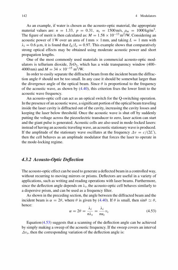
142 4 Modulators
As an example, if water is chosen as the acousto-optic material, the appropriatematerial values are: n = 1.33, p = 0.31, us = 1500m/s, ρm = 1000kg/m3.The figure of merit is then calculated as: M = 1.58 × 10⁻¹³ m2/W. Considering anacoustic power of 1W over an area of 1mm × 1mm, and taking L = 1 mm withλi = 0.6 µm, it is found that Id/Io = 0.97. This example shows that comparativelystrong optical effects may be obtained using moderate acoustic power and shortpropagation lengths.
One of the most commonly used materials in commercial acousto-optic mod-ulators is tellurium dioxide, TeO2, which has a wide transparency window (400–4000nm) and M = 34 × 10−15 m2/W.
In order to easily separate the diffracted beam from the incident beam the diffrac-tion angle θ should not be too small. In any case it should be somewhat larger thanthe divergence angle of the optical beam. Since θ is proportional to the frequencyof the acoustic wave, as shown by (4.40), this criterion fixes the lower limit to theacoustic wave frequency.
An acousto-optic cell can act as an optical switch for the Q-switching operation.In the presence of an acoustic wave, a significant portion of the optical beam travelinginside the laser cavity is diffracted out of the cavity, increasing the cavity losses andkeeping the laser below threshold. Once the acoustic wave is shut off by suddenlyputting the voltage across the piezoelectric transducer to zero, laser action can startand the giant pulse is generated. Acoustic cells are also used in mode-locked lasers:instead of having an acoustic travelingwave, an acoustic stationarywave is produced.If the amplitude of the stationary wave oscillates at the frequency Δν = c/(2L′),then the cell behaves as an amplitude modulator that forces the laser to operate inthe mode-locking regime.
4.3.2 Acousto-Optic Deflection
The acousto-optic effect can be used to generate a deflected beam in a controlledway,without recurring to moving mirrors or prisms. Deflectors are useful in a variety ofapplications, such as writing and reading operations with laser beams. Furthermore,since the deflection angle depends on λi, the acousto-optic cell behaves similarly toa dispersive prism, and can be used as a frequency filter.
As shown in the preceding section, the angle between the diffracted beam and theincident beam is α = 2θ , where θ is given by (4.40). If θ is small, then sinθ θ ,hence:
α = 2θ = λi
nλs= λi
nusνs (4.53)
Equation (4.53) suggests that a scanning of the deflection angle can be achievedby simply making a sweep of the acoustic frequency. If the sweep covers an intervalΔνs, then the corresponding variation of the deflection angle is:

4.3 Acousto-Optic Effect 143
Δα = λi
nusΔνs. (4.54)
The important figure here is the number of distinguishable angular positions, N ,determined by the ratio between Δα and the angular divergence of the laser beam.θo = λi/(πw), w being the radius of the Gaussian beam. The ratio is:
N = Δα
θo= Δνsτ, (4.55)
where τ = w/us is the transit time of the acoustic wave across the light beam. Asan example, if us = 1500 m/s (water), w = 5 mm, νs is swept from 80 to 125 MHz(Δνs = 45 MHz), one finds: N = 150.
There is an important conceptual point that should be clarified. If both ki andthe direction of ks are kept fixed, then the condition (4.43), which graphically cor-responds to the closure of the triangle in Fig. 4.12, does not give any degree offreedom: diffraction is obtained at one acoustic frequency only. This would implythat one would not get any diffracted beam during a sweep of the acoustic frequency,except at that instant in which the acoustic wave vector satisfies the equality (4.43).How can this problem be overcome? The key to the solution lies in the observa-tion that the acoustic wave is not truly a plane wave. It is transversally limited to afinite cross-section, and this results in a spread in the direction of ks, as depicted inFig. 4.13. Therefore, as νs is changed, it may still be possible to close the triangleof wave vectors by exploiting a component of the acoustic wave that has a differentdirection.
Fig. 4.13 Acousto-optic deflection

144 4 Modulators
Problems
4.1 Consider the electro-optic amplitude modulator of Fig. 4.2, using a lithium nio-bate crystal. The operating wavelength is λ = 1530 nm, the electro-optic crystal islithium niobate, the crystal length is L = 6 cm, the crystal thickness is d = 40 µm,and the output intensity IB is equal to zerowhen no voltage is applied to the crystal. (i)Calculate the value of the applied voltage Vπ required to obtain 100% transmissionat input B; (ii) Calculate the upper limit to the modulation frequency, as determinedby the condition that the transit time of the light beam through the crystal be onefifth of the modulation period.
4.2 Consider the electro-optic amplitudemodulator of Fig. 4.2, using a lithium tanta-late crystal. The operatingwavelength isλ = 1550 nm, the crystal length isL = 4 cm,the crystal thickness is d = 40 µm, and the output intensity IB is equal to zero whenno voltage is applied to the crystal. Assume that the applied voltage V is the sumof a bias voltage Vo plus a signal voltage V1. Calculate: (i) the value of Vo requiredto bring the modulator in the linear regime; (ii) the upper limit to V1, subject to thecondition that the maximum output intensity does not exceed the limit of 75% ofthe input intensity.
4.3 A light beam at λ = 1550 nm, linearly polarized along x, propagates along theoptical axis (the z axis) of a KDP crystal. A voltage V is applied to the crystal alongthe z axis. After crossing the crystal the light beam goes through a sequence of aquarter-wave plate, having the optical axis in the x-z plane forming an angle of 45◦with the x axis, and of a polarizer, with optical axis along y. Calculate the valueof V required for a 100% transmission of the incident beam through the sequencecrystal-plate-polarizer.
4.4 An amplitude modulator based on the electro-optic Kerr effect can be made byputting the Kerr cell in between two crossed polarizers, as in Fig. 4.6. The externalelectric field E′ is applied transversally, and the incident light is linearly polarized at45◦ to the electric field. Calculate the half-wave voltage Vπ/2 by assuming that thewavelength of light is 600 nm, the path-length of the light beam inside the Kerr cellis 5 cm, the distance between the two capacitor plates is 2 mm, and the electro-opticmaterial is liquid nitrobenzene (ne
K − noK = 2.6 × 10⁻¹⁸ m2/V2).
4.5 A light beam at λ = 1500 nm goes through an acousto-optic cell made of flintglass (us = 3 km/s, n = 1.95) in which an acoustic wave of frequency 200 MHzis propagating. Calculate: (i) the wavelength difference between the diffracted waveand the incident wave; (ii) the deflection angle of the diffracted wave.
4.6 A light beam at λ = 650 nm goes through an acousto-optic cell made of water(n = 1.33, p = 0.31, us = 1500 m/s, ρ = 1000 kg/m3) having a square cross-section. Calculate: (i) the frequency of the acoustic wave producing a deflection angleof 2◦; (ii) the acoustic power required to transfer all the input power to the diffractedbeam.

Chapter 5Semiconductor Devices
Abstract Themost important family of photonic devices is based on semiconductormaterials. Semiconductor lasers have high efficiency and long lifetime, are fabricatedby the same epitaxial growth techniques used in silicon microelectronics, can bedesigned to emit at almost any wavelength in the visible and near infrared range.In this chapter, after an introduction to the optical properties of semiconductors,the double-heterojunction structures used for semiconductor lasers are described,along with the main characteristics of laser emission. The subsequent sections dealwith semiconductor amplifiers and light emitting diodes. The last part of the chapterconcerns photodetectors and electro-absorption modulators.
5.1 Optical Properties of Semiconductors
The lasers described in Chap.3 are based on transitions among energy levels ofsingle atoms (or ions or molecules). In the case of semiconductor lasers the situationis different because the involved energy levels belong to the whole crystal, and notto a single atom.
In this section, a very simplified qualitative picture of the optical properties ofsemiconductors is given, with the aim of offering an intuitive description of themain processes involved in the interactions between a semiconductor crystal andan optical wave. From a phenomenological point of view semiconductors are solidswhose electrical conductivity is typically intermediate between that of a metal andthat of an insulator. Their conductivity can significantly increase by increasing thetemperature or doping the material with impurities.
The atoms in a crystal lattice are strongly interacting. As a result, instead ofindividual energy levels, energy bands belonging to the whole crystal are formed. Inthe absence of external excitations, the bands are either fully occupied by electrons orare totally unoccupied (except for the special case ofmetals). Thehighest-energy fullyoccupied band is known as the valence band, while the lowest-energy unoccupiedband is called the conduction band. These two bands are separated by a forbiddenenergy band, with bandgap energy Eg . Values of Eg for various semiconductors aregiven in Table5.1.
© Springer International Publishing Switzerland 2016V. Degiorgio and I. Cristiani, Photonics, Undergraduate Lecture Notes in Physics,DOI 10.1007/978-3-319-20627-1_5
145

146 5 Semiconductor Devices
Table 5.1 Properties of some semiconductors
Semiconductor Eg (eV) λg(µm) Type of gap
Ge 0.66 1.88 I
Si 1.11 1.15 I
AlP 2.45 0.52 I
AlAs 2.16 0.57 I
AlSb 1.58 0.75 I
GaP 2.26 0.55 I
GaAs 1.45 0.85 D
GaSb 0.73 1.70 D
GaN 3.45 0.36 D
InN 2.00 0.62 D
InP 1.35 0.92 D
InAs 0.36 3.50 D
InSb 0.17 7.30 D
In the fourth column I and D indicate, respectively, indirect bandgap and direct bandgap
At an absolute temperature of zero, an ideal semiconductor crystal has zero electricconductivity because there are no free charge carriers. An external energy source canexcite an electron, causing a transition from the valence band to the conduction band.The transition leaves a hole in the valence band. Both electrons in the conductionband and holes in the valence band are mobile charge carriers contributing to theelectric conductivity of the crystal.
The absorption of a photon with an energy of hν ≥ Eg excites an electron to theconduction band. By analogy with the case of an isolated atom, one could expectthat the excited electron decays spontaneously to the valence band by emitting aphoton. The situation inside the crystal is, however, more complicated, because theelectronmust be treated as a wave-like particle, with a wave-vector k andmomentump = hk/(2π). Near the bottom of the conduction band, the energy versusmomentumrelation is approximately parabolic:
E = Ec + h2k2
8π2mc, (5.1)
where mc, called effective mass of the electron, is different from the free electronmass me because of the effect of the interactions with the ions of the crystal lattice. Asimilar energy-momentum relation can bewritten for holes near the top of the valenceband. The illustration in Fig. 5.1 qualitatively shows the band structures of two semi-conductors, Si and GaAs. In the case of Si , the minimum of the conduction band andthe maximum of the valence band do not occur at the same k value. A semiconduc-tor that has such a band characteristic is called an indirect-bandgap semiconductor.

5.1 Optical Properties of Semiconductors 147
Fig. 5.1 Transitions in direct- and indirect-gap semiconductors
In contrast, a semiconductor like GaAs is a direct-bandgap semiconductor, becausethe minimum of the conduction band and the maximum of the valence band occurat the same k value. Table5.1 indicates that both silicon (Si) and germanium (Ge)are indirect-bandgap materials, whereas several semiconductors made by combininga trivalent with a pentavalent atom, known as III–V semiconductors, have a directbandgap. By absorbing a photon, the electron takes up not only the energy, but alsothe momentum of the photon. The order of magnitude of electron wave-vectors isk ≈ 2π/a, where a ≈ 10−8 cm is the crystal lattice constant. The modulus of thephoton wave-vector is 2π/λ. In the case of visible or near infrared light, λ is aboutfour orders of magnitude larger than a, so that it can be said that the electron momen-tum is practically unchanged by the photon absorption process. Therefore, as shownin Fig. 5.1, the transition from the valence band to the conduction band is vertical inthe E, k plane.
As a general rule the excited electron will always go to occupy the lowest energylevel in the conduction band. In correspondence, the hole will go to the highestavailable level in the valence band. To ensure momentum conservation, the decay ofthe excited electron to the valence band (also called electron-hole recombination) canbe radiative (that is, a photon is emitted) only if the bottom of the conduction bandcorresponds to the top of the valence band, i.e. if they have the same wave-number.The maximum wavelength of light that can be absorbed (and emitted) by a givensemiconductor is:
λg = hc
Eg. (5.2)
Values of λg are reported in Table5.1. In the case of indirect-bandgap, the excitedelectron quickly relaxes to the bottom of the conduction band, by making an intra-band transition in which energy and momentum are exchanged with the crystallattice. At that point the electron-hole recombination is non-radiative, and involvesthe creation of a phonon.
In an undoped semiconductor (usually called an “intrinsic” semiconductor), attemperature T , there are always some electron-hole pairs, due to thermal excitation.The electron concentration ni is equal to the hole concentration pi . Both concentra-tions are small at room temperature, because kB T � Eg .
148 5 Semiconductor Devices
A large concentration of conduction electrons can be created by doping the semi-conductor with “donor” atoms having excess valence electrons with respect to thesemiconductor. As an example, silicon, which is a tetravalent element, becomes ann-type semiconductor when a small amount of pentavalent atoms, such as phos-phorus (P) or arsenic (As), are added to it. The impurity atom needs only four ofits outer-shell electrons to bind with the neighboring Si atoms. This leaves its fifthelectron only loosely bound, and free to move into the conduction band, after aroom-temperature thermal excitation. In a similar way, n-type gallium arsenide canbe created by doping the GaAs with an element from the sixth column of the peri-odic table, such as selenium (Se), which substitutes for an As atom in the lattice. Toform p-type semiconductors with large hole populations, the crystal is doped with“acceptor” elements, having a deficiency of valence electrons with respect to thesemiconductor.
By itself, a doped semiconductor is not better than the intrinsic one, from thepoint of view of light emission. In fact it can be shown that the product of theelectron and hole concentrations, n and p, is constant for a given semiconductor atfixed temperature, that is, np = ni pi . The application of this law to an n-dopedsemiconductor shows that, when n is above ni , p becomes smaller than pi . Since thenumber of recombination processes is proportional to the product np, the number ofemitted photons is independent of the doping of the semiconductor.
5.2 Semiconductor Lasers
Efficient light emission from a direct-bandgap semiconductor requires the presenceof a large population of both type of carriers in the same crystal region. Such acondition can be realized in the depletion region of a p-n junction. Semiconductorlasers, which are currently the most important class of lasers, are based on forward-biased junctions. For this reason they are also known as diode lasers.
5.2.1 Homojunction Laser
In an n-type semiconductor at low temperature electrons occupy all the energy statesof the valence band plus the lower energy states of the conduction band up to amaximum level, EFn , known as the Fermi energy. In a similar way, inside a p-typesemiconductor electrons occupy the energy levels up to a maximum level, EFp,known as the Fermi energy of the p-type semiconductor, which is located insidethe valence band. When a p-type and an n-type regions are brought into contact,electrons diffuse from the n-region into the p-region, and holes diffuse in the oppositedirection. After a short transient period, in which recombination processes occur in anarrow region on both sides of the junction, a steady-state is reachedwhen this region,known as the depletion-layer, is completely depleted of mobile charge carriers. A
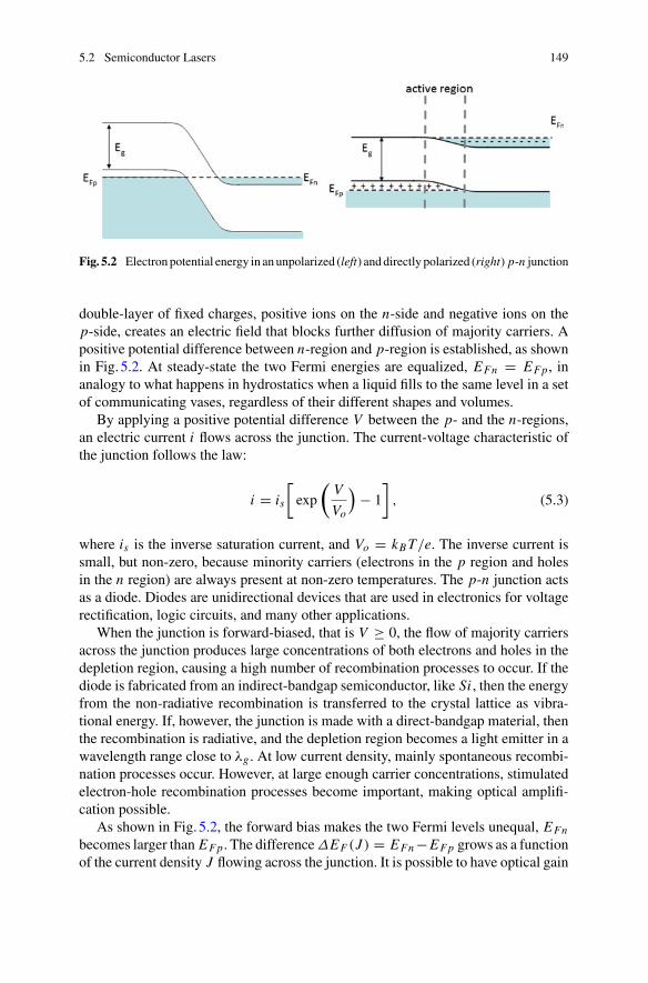
5.2 Semiconductor Lasers 149
Fig. 5.2 Electron potential energy in anunpolarized (left) anddirectly polarized (right) p-n junction
double-layer of fixed charges, positive ions on the n-side and negative ions on thep-side, creates an electric field that blocks further diffusion of majority carriers. Apositive potential difference between n-region and p-region is established, as shownin Fig. 5.2. At steady-state the two Fermi energies are equalized, EFn = EFp, inanalogy to what happens in hydrostatics when a liquid fills to the same level in a setof communicating vases, regardless of their different shapes and volumes.
By applying a positive potential difference V between the p- and the n-regions,an electric current i flows across the junction. The current-voltage characteristic ofthe junction follows the law:
i = is
[exp
(V
Vo
)− 1
], (5.3)
where is is the inverse saturation current, and Vo = kB T/e. The inverse current issmall, but non-zero, because minority carriers (electrons in the p region and holesin the n region) are always present at non-zero temperatures. The p-n junction actsas a diode. Diodes are unidirectional devices that are used in electronics for voltagerectification, logic circuits, and many other applications.
When the junction is forward-biased, that is V ≥ 0, the flow of majority carriersacross the junction produces large concentrations of both electrons and holes in thedepletion region, causing a high number of recombination processes to occur. If thediode is fabricated from an indirect-bandgap semiconductor, like Si , then the energyfrom the non-radiative recombination is transferred to the crystal lattice as vibra-tional energy. If, however, the junction is made with a direct-bandgap material, thenthe recombination is radiative, and the depletion region becomes a light emitter in awavelength range close to λg . At low current density, mainly spontaneous recombi-nation processes occur. However, at large enough carrier concentrations, stimulatedelectron-hole recombination processes become important, making optical amplifi-cation possible.
As shown in Fig. 5.2, the forward bias makes the two Fermi levels unequal, EFn
becomes larger than EFp. The differenceΔEF (J ) = EFn −EFp grows as a functionof the current density J flowing across the junction. It is possible to have optical gain

150 5 Semiconductor Devices
Fig. 5.3 Structure of the homojunction laser
only if ΔEF (J ) becomes larger than Eg . Precisely, light emission occurs in thefrequency band determined by the condition:
ΔEF (J ) ≥ hν ≥ Eg. (5.4)
Equation (5.4) can be seen as the condition for population inversion in the current-injected semiconductor.
The first semiconductor laser was operated in 1962 using a Ga As p-n junction.Since a junction in which the same material is used for both the p and the n sidesis called a homojunction, this laser is known as a homojunction laser. The lightemission was in the near infrared, at a wavelength close to λg = 0.85µm. The basicstructure of the homojunction laser is shown in Fig. 5.3. The electric current flowsalong the x axis. The active region is the depletion layer with a length of 0.2–0.5 mmand a width, in the y direction, of 0.1–0.2 mm. The thickness of the active layer alongx is very small, typically around 1 µm.
The feedback needed for laser action inside the Fabry-Perot cavity is providedby the reflections from the two parallel end faces, which are prepared by cleavagealong a crystal plane. Since the refractive index of a semiconductor is fairly large,the refractive-index mismatch at the air-semiconductor interface gives a sufficientlyhigh reflectance without the need for reflective coatings of the end facets. As anexample, the refractive index of GaAs is n = 3.6, so that the reflectance from (2.34)is R ≈ 30%.
The homojunction laser was operated continuously at the liquid nitrogen tem-perature (T = 77 K), with a threshold current density Jth ≈ 1 kA/cm2. When Tis increased, more and more electrons can occupy energy states above Fermi lev-els. This has the effect of reducing the optical gain. It can be shown that Jth growsexponentially with T , according to the law:
Jth(T ) = Jth(To) exp
(T
To− 1
). (5.5)
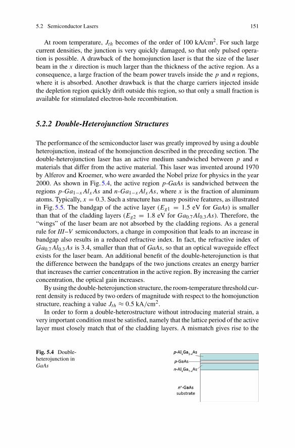
5.2 Semiconductor Lasers 151
At room temperature, Jth becomes of the order of 100 kA/cm2. For such largecurrent densities, the junction is very quickly damaged, so that only pulsed opera-tion is possible. A drawback of the homojunction laser is that the size of the laserbeam in the x direction is much larger than the thickness of the active region. As aconsequence, a large fraction of the beam power travels inside the p and n regions,where it is absorbed. Another drawback is that the charge carriers injected insidethe depletion region quickly drift outside this region, so that only a small fraction isavailable for stimulated electron-hole recombination.
5.2.2 Double-Heterojunction Structures
The performance of the semiconductor laser was greatly improved by using a doubleheterojunction, instead of the homojunction described in the preceding section. Thedouble-heterojunction laser has an active medium sandwiched between p and nmaterials that differ from the active material. This laser was invented around 1970by Alferov and Kroemer, who were awarded the Nobel prize for physics in the year2000. As shown in Fig. 5.4, the active region p-GaAs is sandwiched between theregions p-Ga1−x Alx As and n-Ga1−x Alx As, where x is the fraction of aluminumatoms. Typically, x = 0.3. Such a structure has many positive features, as illustratedin Fig. 5.5. The bandgap of the active layer (Eg1 = 1.5 eV for GaAs) is smallerthan that of the cladding layers (Eg2 = 1.8 eV for Ga0.7Al0.3As). Therefore, the“wings” of the laser beam are not absorbed by the cladding regions. As a generalrule for III–V semiconductors, a change in composition that leads to an increase inbandgap also results in a reduced refractive index. In fact, the refractive index ofGa0.7Al0.3As is 3.4, smaller than that of GaAs, so that an optical waveguide effectexists for the laser beam. An additional benefit of the double-heterojunction is thatthe difference between the bandgaps of the two junctions creates an energy barrierthat increases the carrier concentration in the active region. By increasing the carrierconcentration, the optical gain increases.
Byusing the double-heterojunction structure, the room-temperature threshold cur-rent density is reduced by two orders of magnitude with respect to the homojunctionstructure, reaching a value Jth ≈ 0.5 kA/cm2.
In order to form a double-heterostructure without introducing material strain, avery important conditionmust be satisfied, namely that the lattice period of the activelayer must closely match that of the cladding layers. A mismatch gives rise to the
Fig. 5.4 Double-heterojunction inGaAs
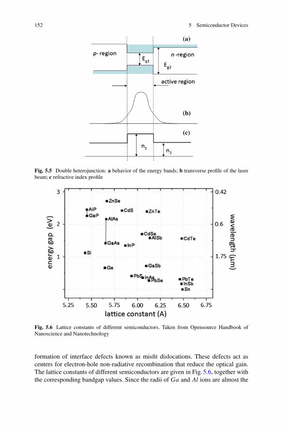
152 5 Semiconductor Devices
Fig. 5.5 Double heterojunction: a behavior of the energy bands; b transverse profile of the laserbeam; c refractive index profile
Fig. 5.6 Lattice constants of different semiconductors. Taken from Opensource Handbook ofNanoscience and Nanotechnology
formation of interface defects known as misfit dislocations. These defects act ascenters for electron-hole non-radiative recombination that reduce the optical gain.The lattice constants of different semiconductors are given in Fig. 5.6, together withthe corresponding bandgap values. Since the radii of Ga and Al ions are almost the

5.2 Semiconductor Lasers 153
Fig. 5.7 Thedouble-heterojunction laser:stripe-geometryconfiguration
same, the lattice periods of GaAs and AlAs coincide, and thus lattice-matching forthe GaAs/GaAlAs structure is very good. In the case of the quaternary compoundGa1−x I nx As1−y Py , which is used for optical-communications lasers, the alloy canbe lattice-matched to cladding layers made of InP by choosing a specific y/x ratio.It is found that the optimal value is y = 2.2 x .
Stripe geometry.Double-heterojunction lasers oftenuse the so-called stripe-geometryconfiguration shown in Fig. 5.7. By introducing an insulating oxide layer, currentfrom the positive electrode is constrained to flow in a narrow stripe. By reducingthe cross-section, the total current is correspondingly reduced for a given currentdensity. Another method to reduce the cross-section is that of creating a refractiveindex profile that produces a confinement along the y-direction, as is the case forboth the “channeled substrate laser”, and “buried heterostructure laser” structures.The size of the active region along y can be as small as a few µm, with a thresholdcurrent, ith , around 10 mA and applied voltage of 1.5–2 V.
Distributed feedback. As it has been discussed in Sect. 3.6, a Fabry-Perot lasercan operate with more than one longitudinal mode. The actual number of oscillatingmodes is determinedby the ratio between the frequencybandΔνL of the amplifier andthe distance Δν between two adjacent longitudinal modes. In several applications,among which optical communications is the most important, emission at a singlefrequency is necessary. Among the different methods to realize a single-mode semi-conductor laser, the distributed feedback geometry is themostwidely used. Figure5.8shows the scheme of a distributed feedback laser, also known as DFB laser, whichconsists of an active medium in which a periodic thickness variation is introduced inone of the cladding layers. The periodic corrugation provides optical feedback for thelaser oscillation, and the end facets are coated with antireflection coatings. The laserbehaves as an optical amplifier in which the forward and the backward beam have afrequency-selective coupling. These two counter-propagating beams are efficientlycoupled to each other only if their wavelength is such that
λ = 2neff Λ (5.6)
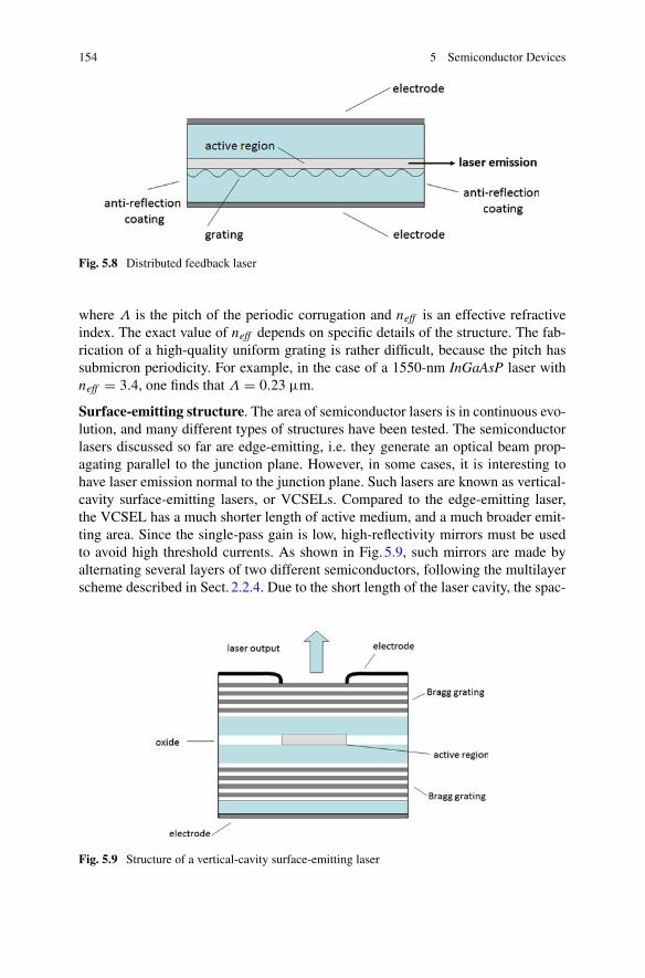
154 5 Semiconductor Devices
Fig. 5.8 Distributed feedback laser
where Λ is the pitch of the periodic corrugation and neff is an effective refractiveindex. The exact value of neff depends on specific details of the structure. The fab-rication of a high-quality uniform grating is rather difficult, because the pitch hassubmicron periodicity. For example, in the case of a 1550-nm InGaAsP laser withneff = 3.4, one finds that Λ = 0.23 µm.
Surface-emitting structure. The area of semiconductor lasers is in continuous evo-lution, and many different types of structures have been tested. The semiconductorlasers discussed so far are edge-emitting, i.e. they generate an optical beam prop-agating parallel to the junction plane. However, in some cases, it is interesting tohave laser emission normal to the junction plane. Such lasers are known as vertical-cavity surface-emitting lasers, or VCSELs. Compared to the edge-emitting laser,the VCSEL has a much shorter length of active medium, and a much broader emit-ting area. Since the single-pass gain is low, high-reflectivity mirrors must be usedto avoid high threshold currents. As shown in Fig. 5.9, such mirrors are made byalternating several layers of two different semiconductors, following the multilayerscheme described in Sect. 2.2.4. Due to the short length of the laser cavity, the spac-
Fig. 5.9 Structure of a vertical-cavity surface-emitting laser

5.2 Semiconductor Lasers 155
Fig. 5.10 Active layer of a semiconductor laser made of a multiple quantum well, with a composi-tion given by I n0.5Ga0.5P/I n0.5Ga0.5−x Alx P. The plot represents the behavior of the Al fraction,x , across the junction
ing of Δν between adjacent longitudinal modes is very large. Thus, if the frequencyof one mode coincides with the peak reflectivity of the multilayer mirrors, the twoadjacent modes fall outside the high-reflectivity band of the mirrors, and single-longitudinal-mode operation is achieved. By limiting the diameter of the emissionarea to 5–10µm, a very low threshold current is obtained (ith ≈ 1mA). Correspond-ingly, the output power is also small, typically of the order of 1 mW. However, it ispossible to build large-area (300 µm diameter) VCSELs with output power of watts.
Multiple-quantum-well. A very interesting concept recently emerged in many dis-tinct scientific and technological areas is the use of artificially tailored structures atthe nanoscale. It is beyond the scope of this text to explain the properties of nanostruc-tured materials, but the important aspect is that electrons confined in nanostructureshave discrete energy levels, instead of continuous, with the energy of those levelsfixed by the geometry of the structure, following the rules of quantummechanics. Asan example, Fig. 5.10 shows the nanostructured active layer of a semiconductor laser,in which the active region consists of a number of alternating layers of narrow andwide bandgap materials. The thickness of the narrow-bandgap layers (the “quantumwells”) and that of the wide-bandgap barriers are both about 5 nm. A laser of thistype is known as a “multiple quantum well” (MQW) laser. MQW lasers are realizedin both edge-emitting and surface-emitting configurations. In general, they have avery low threshold current density and a high efficiency. They also have a very stableemission wavelength, not influenced by changes in electric current or temperature.
5.2.3 Emission Properties
Laser emission has been obtained from many different III–V semiconductors.Table5.2 lists the most common semiconductor lasers. The trivalent atom can begallium or aluminum or indium. The pentavalent atom can be arsenic or phosphorusor antimony (Sb) or nitrogen (N ). By using combinations of two trivalent atomsand/or two pentavalent ones, the emission wavelength can be tuned, in some cases,

156 5 Semiconductor Devices
Table 5.2 Operating wavelength range of semiconductor lasers
Compound λ (µm) Compound λ (µm)
I nx Ga1−x N 0.37–0.50 Ga0.42 I n0.58As0.9P0.1 1.55
Ga1−x Alx As 0.62–0.85 I nGa AsSb 1.7–4.4
Ga0.5 I n0.5P 0.67 PbCd S 2–4
Ga0.8 I n0.2 As 0.98 PbSSe 4.2–8
Ga1−x I nx As1−y Py 1.10–1.65 PbSnSe 8–32
Ga0.27 I n0.73 As0.58P0.42 1.31 Quantum cascade 2–70
over a very broad range. This is a distinctive property of semiconductor lasers: solid-state and gas lasers operate at discrete wavelengths fixed by the position of atomic orionic energy levels (with a few exceptions), but semiconductor lasers can be designedto operate at essentially any wavelength in the visible and near infrared.
The wavelength range 0.62–0.85 µm is covered by devices using Ga1−x Alx As.Since the lattice constant of Ga1−x Alx As does not depend on the fraction x of Alatoms (see Fig. 5.6), heterojunctions containing any fraction of Al can be grownepitaxially. A limit to using large values of x comes from the fact that the compoundacquires an indirect bandgap when x ≥ 0.7. Ga1−x Alx As lasers emitting at 0.81µmhave an important application for pumping Nd-YAG lasers, as described in Sect. 3.9.Optical-communication lasers, emitting around 1.31 or 1.55 µm are based on thequaternary compound Ga1−x I nx As1−y Py grown on top of InP. By changing thefractions x and y, it would be possible to cover awide range of bandgap energies, from0.4 to 2.2 eV. In practice, because of the mismatch in atomic sizes between galliumand indium, and also between arsenic and phosphorus, only the range 0.7–1.4 eV(λ = 0.88–1.76 µm) can be usefully covered. The Ga0.8 I n0.2As laser, emitting at0.98 µm, has an important role as the pump of the fiber-optic amplifier describedin the following chapter. III-V semiconductors using nitrogen as the pentavalentatom exhibit a large bandgap, and so can emit blue and violet light. In particular,the wavelength range 0.37–0.50 µm is covered by the I nx Ga1−x N laser, which isuseful for a variety of applications, such as writing and reading Blu-ray optical discs.
By using II–V I semiconductors, lasers operating in the mid- and far-infraredrange of wavelengths can be made. Sources in this range of wavelengths are use-ful for such applications as chemical sensing and trace-gas analysis. Since the laserefficiency strongly decreases when the photon energy becomes comparable to kB T ,all these devices work at cryogenic temperatures. The same wavelength range canbe covered much more efficiently by a new family of semiconductor lasers, termedquantum cascade lasers (QCL), which make use of MQW structures in III–V semi-conductors. It goes beyond the scope of this text to describe the physical mecha-nism of QCLs, which is completely different from that of diode lasers. It suffices tomention that the QCL can be designed to emit at any wavelength in the mid- andfar-infrared, through appropriate choice of the nanostructure. The QCL can operateat room temperature as a continuous source or as a source of picosecond pulses.

5.2 Semiconductor Lasers 157
Fig. 5.11 Output powerversus input current for adouble-heterojunction laser,at three differenttemperatures
A double-heterojunction laser has an internal efficiency, defined as the ratiobetween the number of radiative recombinations and the number of injected electron-hole pairs, that can be close to 100%. The overall efficiency of the laser, definedas the ratio between emitted optical power and injected electric power, often termed“wall-plug efficiency”, can be as large as 50%.
Experimental curves of output power versus input current, at three different tem-peratures, are shown in Fig. 5.11. It is found that the threshold current grows withincreasing the temperature, as predictedby (5.5)with abest-fit parameterTo ≈ 160K.
The output beam of a semiconductor laser is usually strongly diverging, becauseof the smallness of the transverse size of the active region. Typically, the beamobserved at the output facet of a GaAs laser has an elliptical cross-section with a sizeof 1µm in the direction orthogonal to the junction (x direction), and of 10 µm in they direction. The far-field angular spread due to diffraction is about 50◦ along x and5◦ along y. By using a cylindrical lens with two different focal lengths along x andy, the beam can be collimated to obtain a circular spot having a divergence angle ofjust a few milliradians.
The spectrumof the laser emissionhas a peakwavelengthλp that depends onpumpcurrent and temperature. The wavelength interval ΔλL over which laser oscillationcan occur grows as the pump current increases, as described by (5.4). Some typicalvalues of ΔλL are reported in Table5.3. If ΔλL grows and, at the same time, thehighest emission wavelength remains fixed to hc/Eg , then the central wavelength
Table 5.3 Spectral properties of three semiconductor lasers
λ = 850 nm λ = 1300 nm λ = 1550 nm
ΔλL in nm 2.0 5.0 7.0
Δλ in nm 0.27 0.6 0.9
dλp/dT in nm/◦C 0.22 0.5 0.73
dλq/dT in nm/◦C 0.06 0.12 0.18

158 5 Semiconductor Devices
of the emission spectrum, λp, decreases with increasing pump current, at fixedtemperature.
Since Eg is a decreasing function of T , λp grows with T . Some typical valuesof the derivative dλp/dT are reported in Table5.3. Clearly, in order to stabilize theemission wavelength, precise temperature control is needed.
Table5.3 also shows typical values for the wavelength separation between twoadjacent longitudinal modes, which, according to Sect. 3.6, is expressed as Δλ =λq −λq−1 ≈ λp
2/(2L ′). The optical path L ′ is very short in the semiconductor laser,so that themodes are rather widely spaced. However the bandwidthΔλL is also large.As a consequence, the laser usually oscillates on several modes. Using the data inTable5.3, the number of oscillatingmodes, as calculated from N = ΔλL/Δλ, is 7–8.Since the index of refraction of semiconductors increases with T , the wavelength ofthe generic qth mode also increases with T . Values of dλq/dT are reported in thelast row of the same table.
The CW output power of a semiconductor laser can only be several hundreds ofmilliwatts, at most. By fabricating a two-dimensional array of lasers on a single sub-strate, and then coupling all the outputs into a single optical fiber, a monochromaticoptical power of several tens of watts can be achieved. This scheme is often used topump solid-state and fiber lasers.
An important feature of a semiconductor laser is its very long lifetime: as anexample, a test conducted on a set of GaAlAs lasers, operating at 70 ◦C with anoutput power of 5 mW, has measured a lifetime of 30,000h (3.5years of continuousoperation). GaInAsP lasers have been found to have even longer lifetimes.
By pulsing the pump, a semiconductor laser can be made to emit short pulses, foruse, as an example, in portable optical radars. It can also be intensity modulated bycontrolling the pump current. The modulating signal (typically 40–60 mA peak-to-peak) is superposed to the direct bias current. Themaximum frequency ofmodulationdepends on how quickly the carrier density in the active region can be varied. Typicalvalues are of the order of a few GHz, but, in specially designed devices, modulationfrequencies of 20–30 GHz have been demonstrated.
Diode lasers can also generate ultrashort pulses, using either active or passivemode-locking. Typically, pulse-widths of between 0.5 and 5 ps with repetition ratesof between 1 and 100 GHz can be obtained. For repetition rates below roughly10 GHz, an external cavity setup is generally required. Particularly interesting are thevertical-external-cavity surface-emitting lasers (VECSELs), which have a vertical-cavity surface-emitting structure with one of the two high-reflecting mirrors externalto the diode structure. Typical cavity lengths are from a few millimeters up to tens ofcentimeters. The gain chip generally contains a highly reflective bottom section toreflect the laser and pump light, an active semiconductor gain section, and an anti-reflective top layer. By passively mode-locking optically pumped VECSELs, it ispossible to obtain much higher pulse energies than those generated by edge-emittingstructures.

5.3 Semiconductor Amplifiers 159
5.3 Semiconductor Amplifiers
A semiconductor optical amplifier, usually known as SOA, is realized by eliminatingthe feedback elements in a semiconductor laser, usually by putting an anti-reflectioncoating on the two facets of the active region. Of course, the operating wavelengthsof SOAs are the same as those of the corresponding lasers, listed in Table5.2.
Typically, at λ = 1.55 µm, the gain per unit length g is of the order of 105 m−1
and the gain bandwidth is about 10 THz. Since g is somewhat dependent on thepolarization state of the input signal, a simple SOA does not generally preserve theinput polarization. However, it is possible to implement more complex amplifyingschemes that are polarization-preserving.
SOAs are attractive for many applications because they are small, have a largeoptical gain, and can be driven by a low-voltage supply. However, the small size ofthe active region makes the input coupling rather critical, while the large gain cangive rise to signal distortions because of saturation effects.
The most important applications of SOAs are in the optical-communication area,as will be discussed in Chap. 8.
5.4 Electroluminescent Diodes
The electroluminescent diodes fabricated from semiconductors are known as lightemitting diodes (LEDs). An LED is a solid-state light source using the spontaneousemission generated by radiative electron-hole recombinations in the active region ofthe diode under forward bias. Unlike a laser, an LED does not have an optical cavityor a threshold current. It starts emitting light as soon as a forward bias voltage isapplied to the junction, and emits incoherent and unpolarized spontaneous photons.As in a laser, the emission wavelength is determined by the bandgap energy of theused semiconductor. An other important electroluminescent diode is the organiclight-emitting diode, known as OLED, which is based on organic compounds.
5.4.1 LEDs
The first visible LED, emitting at 710nm, was demonstrated by Holonyak in1962 using a GaAsP diode. After this realization the research concerning electro-luminescent materials was extended to many different III–V semiconductors. Animportant step was made in 1994 with the invention of the blue LED. Akasaki,Amano, and Nakamura were awarded the Nobel prize in Physics in the year 2014for this invention. The light emitted by an LED has a wavelength λg = hc/Eg , anda bandwidth Δλ given by:

160 5 Semiconductor Devices
Fig. 5.12 LED emission inthe three fundamental colors
Δλ = 2kB T λg2
hc(5.7)
As an example, an LED emitting 500-nm light at room temperature, has an emis-sion bandwidth predicted by (5.7) of about 10nm. Commercially available LEDscover the spectral range from the near ultraviolet to the near infrared, with wave-lengths ranging from about 370nm to 1.65µm. As shown in Fig. 5.12, red-orangeLEDs use Ga Asx P1−x , and blue-green LEDs use I n1−x Gax N . The emission wave-length is tuned by changing the composition, which modifies the parameter ofx . Some LEDs even use indirect-bandgap semiconductors doped with impuritiesalthough these offer lower efficiency.
The structure of a surface-emitting LED is shown in Fig. 5.13. Spontaneous emis-sion radiates in all directions, but the downward-emitted light is absorbed, and theextraction of the upward-emitted light is possible only over a limited solid angle.The limitation to extraction efficiency is due to reflection from the semiconductor-airinterface. The spontaneous photons that reach this interface at an angle of incidencelarger than the limit angle θc are totally internally reflected. If the refractive indexof the semiconductor is 3.4, then this critical angle is just 17◦, and so the extrac-tion efficiency is very low. Various techniques can be used to increase the extractionefficiency: the reflectance of the semiconductor-air interface can be reduced by ananti-reflection coating, and the downward-emitted light can be recuperated by usinga transparent substrate associated to a highly-reflecting bottom surface.
An important parameter that characterizes a light source is the ratio betweenemitted optical power and injected current. For a visible LED, this ratio is around0.5 W/A. The overall LED efficiency, η, can be as large as 25%. As a comparison,the efficiency of an incandescent lamp is about 1%. High efficiency also impliesless heat generation and less damage. The lifetime of an LED can reach 50,000h ofcontinuous operation.
LEDs are currently used in a large variety of applications, some of which aredescribed in Chap.8. When an LED replaces traditional lamps, then white lightemission is usually required. White light can be obtained by mixing the emissions

5.4 Electroluminescent Diodes 161
Fig. 5.13 Structure of aGaAsP LED.A layer of Te-doped n–Ga As0.6P0.4 is grown on the substraten–Ga As. The double heterojunction is formed by superposing a layer of Zn-doped p–Ga As0.6P0.4.The LED emits in the upward direction, while the downward emitted light is absorbed by thesubstrate
of three LEDs operating at the three fundamental colors (red-green-blue, RGB).However, in practice, it is oftenmore convenient tomake use of a single blue-emittingLED coated with phosphor molecules. The phosphors absorb the blue emission, andspontaneously re-emit light of a longer wavelength. By mixing different phosphorswith different colors, white light emission is achieved. The design and fabrication ofthis white light source is both simpler and cheaper than a complex RGB system.
5.4.2 OLEDs
In an organic light-emitting diode (OLED), the electroluminescent material is anorganic compound, which is electrically conductive and behaves as an organic semi-conductor. Two thin films of organic semiconductor, forming an organic heterostruc-ture, are sandwiched between two electrodes on a transparent substrate. Electroniccharges are transported and injected into the heterostructure from the electrodes:electrons from the cathode, and holes from the anode. In analogy to the case of semi-conductor devices, the radiative recombination of electron and hole generates light.The wavelength of this emission depends on the band gap of the organic material.OLEDs can be used to produce light of a very wide range of wavelengths by modi-fying the precise structure of the organic material. OLEDs are fabricated from smallorganic molecules or conjugated polymer chains, by using standard techniques ofthin film deposition. These are simpler and less expensive than the epitaxial growthused for fabricating LEDs. The potential applications of OLEDs include thin, low-

162 5 Semiconductor Devices
cost displays with a low driving voltage, wide viewing angle, and high contrast andcolor gamut. Polymer LEDs have the added benefit of offering the possibility forprintable and flexible displays. OLEDs are used to make self-luminous displays forportable electronic devices such as cellular phones, digital cameras, and as a source ofbacklighting for liquid-crystal displays. A recent development is the White OrganicLight-Emitting Diode (WOLED), in which red, green, and blue OLED materials aresandwiched together. WOLEDs have potential for use in television technology andarchitectural lighting.
5.5 Photodetectors
A photodetector is a device that measures optical power by absorbing energy froman optical beam. All photodetectors are square-law detectors that respond to theintensity, rather than the field amplitude, of an optical signal. Commonly used pho-todetectors are based on either thermal effects or electric effects.
Thermal detectors convert the absorbed energy into heat. In a bolometer, light isabsorbed by a metallic or semiconducting resistor, or by a termistor. The tempera-ture variation induces a change in the electric resistance of the absorbing material,which is measured, for instance, by a Wheatstone bridge. Highly sensitive mod-ern bolometers use superconducting absorbers operating at cryogenic temperatures.Another possibility is to use a thermocouple, which is typically made by a ring withtwo bimetallic junctions. If one junction is kept at fixed temperature, and the otheris heated by light absorption, then an electric current flows inside the ring, becauseof an effect known as thermoelectric effect or Seebeck effect. The intensity of theelectric current is proportional to the absorbed optical power. Thermocouples areself powered and require no external form of excitation. In general, the response ofthermal detectors does not depend on the wavelength of the incident radiation. How-ever, they have a slower response time and lower sensitivity, compared to electricdetectors.
More important then thermal detectors are the detectors that use electric effects,which include photoelectric detectors, photoconductors, and photodiodes. They canbe made to be extremely sensitive, and can have response times capable of followingvery fast optical signals.
5.5.1 Photoelectric Detectors
The photoelectric effect is the emission of an electronwhen amaterial absorbs energyfrom a light beam. The emitted electrons are called photoelectrons. The effect wasdiscovered by Hertz in 1887 and explained by Einstein in 1905, for which he was

5.5 Photodetectors 163
awarded the Nobel Prize in 1921. The photoelectron is generated only if the photonenergy hν satisfies the condition:
hν ≥ Ei , (5.8)
where Ei is the ionization energy of the electron inside the material. In the case ofsolids, Ei is usually known as the “work function”. The excess energy, hν − Ei ,is transformed in kinetic energy of the photoelectron. The material can be a gas,a liquid, or a solid. Considering isolated atoms in the ground state, low ionizationenergies are found for elements belonging in the first column of the periodic table,i.e. the alkali metals. This is not surprising because these elements have only oneelectron in their outer electron shell. The cesium atom has the lowest binding energyof Ei = 3.8 eV. The highest binding energy is 24.5 eV for helium, a noble gas.Equation (5.8) states that a photoelectron can only be generated if the wavelength ofthe photon is below a threshold value given by:
λth = hc
Ei. (5.9)
For the cesium atom, λth = 327 nm, which is in the ultraviolet. While no isolatedatom emits photoelectrons under excitation from visible light, the situation is morefavorable for solids. The work function of solid cesium is 1.94 eV, corresponding toa threshold wavelength of λth = 640 nm. Even lower values of the work function arefound for cesium compounds, such as cesium antimonide. The threshold wavelengthcan reach a value of about 1.1 µm, extending the applicability of photoelectricdetectors to the near infrared.
Photoelectric cell. A photoelectric cell, also called a vacuum photodiode, can bemade by collecting the photoelectrons emitted by the photosensitive surface of anegative electrode (photocathode) at a positive electrode (anode). The quantum effi-ciency of the photosensitive surface layer, η, defined as the ratio between the numberof photoelectrons and the number of absorbed photons, can vary between 10−4 and10−1, depending on the incident wavelength and the nature of the surface layer. Thetwo electrodes are placed in a vacuum tube with a transparent window. An electriccurrent flows in a closed circuit configuration under illumination of the photocathode.The photocurrent i ph is obtained by multiplying the electron charge by the numberof photoelectrons collected by the anode per second:
i ph = ηeP
hν, (5.10)
where P is the incident optical power. The sensitivity of the photoelectric cell isexpressed by the ratio i ph/P (Ampère/Watt). As an example, if hν = 2 eV (redlight) and η = 0.1, then the sensitivity is 50 mA/W.

164 5 Semiconductor Devices
Fig. 5.14 Structure of a photomultiplier tube
Photomultiplier tube. The sensitivity of a photoelectric detector can be improvedby many orders of magnitude by multiplying the number of emitted electrons via theprocess of secondary emission. This occurs when the accelerated electrons impactintermediate electrodes, called dynodes, maintained at ever-increasing potential-differences. The resulting device, known as a photomultiplier tube, is schematicallyillustrated in Fig. 5.14. The photocathode contains combinations of materials suchas cesium, rubidium and antimony, specially selected to provide a low ionizationenergy. The number of dynodes varies between 10 and 14. Their shape and posi-tion are designed in order to guide the electrons along trajectories which maximizethe collection efficiency. Typically the potential difference between two successivedynodes is around 100 V and the supply current is around 1 mA. A photoelectronemitted by the photocathode generates m secondary electrons when it impacts thefirst dynode. Each secondary electron, when collected by the second dynode, furtherproduces secondary electrons. If there are n dynodes, then the number of electronsarriving at the anode is mn . Assuming m = 4 and n = 10, the gain of a photomulti-plier tube is: G = mn = 410 ≈ 106. With 14 dynodes, the gain can approach 108. Ifthe quantum efficiency is the same, then the sensitivity of a photomultiplier tube islarger than that of a photoelectric cell by a factor G.
The photoelectric effect has a very short intrinsic response time, comparable tothe oscillation period of the optical field. The response time of the device is limitedby two effects: (i) there is a spread in the transit time of the electrons through themultiplication structure, such that the G electrons produced by a single photoelectrondo not simultaneously reach the anode, but arrive with a spread of a few nanoseconds;(ii) the device has an equivalent capacitance, C , between the anode and the groundthat gives a time constant of RLC , because of the non-zero load resistance RL . IfC = 20 pF and RL = 50 , then the time constant is 1 ns.
A photomultiplier tubewith a gain G = 108 produces an easilymeasurable outputpulse, in response to the absorption of a single photon. Indeed G electrons bunched ina time interval τ give a current pulse with a peak value Ge/τ . Therefore the voltagepulse measured across the load resistance has a peak value GeRL/τ . If G = 108,τ = 1 ns, RL = 50 , then the peak voltage is 0.8 V. When observing the single-photoelectron pulses, very large amplitude variations are found from one pulse to

5.5 Photodetectors 165
the other, because m is not a fixed number, but a statistical variable with a Poissonprobability distribution.
When the optical power incident on the photocathode is so low that the numberof photoelectrons per unit time is less than τ−1, the electric signal at the photomulti-plier output appears as a discrete sequence of pulses. The experimental observationof this discreteness has a great conceptual relevance, because it demonstrates thatelectromagnetic energy is absorbed by matter in quantum steps.
5.5.2 Semiconductor Photodetectors
Semiconductor photodetectors are based on the generation of an electron-hole paircaused by the absorption of a photon. Sometimes this effect is called “internal pho-toelectric effect”, whereas the electron extraction process described in the precedingsection is called external photoelectric effect. The photogeneration of electron-holepairs can be exploited for photodetection purposes in different ways.
Photoconductors. The conductivity of a semiconductor that has electron and holeconcentrations of n and p, respectively, is:
σ = e(μen + μh p), (5.11)
where μe and μh are the electron and hole mobilities, respectively. When a semi-conductor is illuminated with light of a sufficient photon energy, carriers in excessof the equilibrium concentrations are generated. As a consequence, the conductiv-ity increases by an amount that is proportional to the number of photogeneratedelectron-hole pairs. Similarly to the photoelectric effect described in the previoussection, the photoconductivity has a threshold photon energy, and a correspondingthreshold wavelength, λth . For an intrinsic semiconductor, λth is determined by thecondition that the photon energy should be larger than the bandgap energy. Accord-ing to the wavelength to be detected, different semiconductors, such as germanium,silicon, lead sulfide, indium antimonide can be used. In the case of photoconductivedetectors operating at mid-infrared, low temperature operation is necessary, in orderto avoid that the thermal excitation of electron-hole pairs obscures the photoexcita-tion. Instead of using small-bandgap semiconductors, the detection of mid-infraredradiation ismore frequently performed using doped photoconductors.As an example,p-type germanium doped with Zn, cooled at 4K, can detect mid-infrared radiationup to wavelengths of about 40µm.
Photodiodes. A very important category of photodetectors is represented by pho-todiodes. A photodiode is a type of detector capable of converting light into eithercurrent or voltage, depending upon the mode of operation. As discussed in Sect. 5.1,a large internal electric field exists in the depletion layer of a p-n junction. If anelectron-hole pair is generated by photon absorption within this layer, then the twocharge carriers rapidly drift in opposite directions, the electron toward the n region

166 5 Semiconductor Devices
Fig. 5.15 Current-voltage characteristic of a photodiode. Under illumination the characteristicshifts downward by an amount proportional to the light intensity
and the hole toward the p region. If the device is left in an open circuit configuration,then an external potential appears between the p and n regions. This is known asthe photovoltaic effect. The usual way to operate the detector is to apply a reversevoltage across the junction. The current-voltage characteristic expressed by (5.3), asmodified by photon absorption, becomes:
i = is
[exp
( V
Vo
)− 1
]− i ph, (5.12)
where i ph , the photogenerated inverse current, is given by (5.10). As shown inFig. 5.15, the effect of illumination is that of vertically translating the current-voltagecharacteristic. The internal resistance of a photodiode is large, and thus it behavesessentially as a current generator.
Many photodiodes use a structure in which an intrinsic region is interposedbetween the n and p regions. These photodiodes, known as p-i-n photodiodes exhibita larger sensitive volume, and faster response time, with respect to p-n photodiodes.Furthermore the p-i-n structure has a width of the depletion region that is practicallyindependent of the applied voltage.
For the detection of visible and near-infrared radiation silicon photodiodes arethe most common choice, and can have a large efficiency: η = 0.4–0.7. For thewavelength interval 1.0–1.6 µm, InGaAs photodiodes are mostly used.
Avalanche photodiodes. The current-voltage characteristics shown in Fig. 5.15 illus-trate a feature that is not described by (5.12). When the reverse bias voltage is suf-ficiently large, a sudden increase in reverse current is observed. What happens inthis region is that carriers crossing the depletion layer acquire sufficient energy toionize lattice atoms by collision. The carriers produced in this way may, in turn, gen-

5.5 Photodetectors 167
erate further ionizing collisions in a cascade. This mechanism, known as “avalanchebreakdown”, can be destructive if the reverse current is allowed to become too large.
An avalanche photodiode (APD) is a photodiode designed to operate under veryhigh reverse bias, in order to exploit the internal amplification caused by the avalanchebreakdown. The applied voltage is kept slightly below the breakdown voltage, so thatthe APD still behaves as a linear device, giving an output signal proportional to theincident optical power. The actual value of the breakdown voltage depends on thesemiconductor material, device structure and temperature. It is typically around 50 Vfor InGaAs/InP APDs.
Some particular types of APDs can reach such a high gain that they becomesingle-photon detectors, a kind of solid-state photomultiplier tube, but requiring asupply voltage more than one order of magnitude lower than a real photomultipliertube. A possible drawback is that the gain G is rather sensitive to temperature andaging.
5.5.3 CCD Image Sensors
It is possible to convert an optical image into a digital sequence of electrical signalsusing an array of photodetectors. The invention of the charge-coupled-device (CCD)structure represented a real revolution for image recording and transmitting. Boyleand Smithwere awarded theNobel prize in Physics in the year 2009 for this invention.
The photosensitive surface is divided into a two-dimensional array of detectors.The single detector, known as “pixel”, a term coming from the contraction of “pictureelement”, is a metal-oxide-semiconductor (MOS) capacitor. In visible CCD camerasthe semiconductor is doped-silicon. A positive voltage applied between metal andsilicon traps the photogenerated electrons at the silicon surface. The number oftrapped electrons is proportional to the integral of the optical power incident on thepixel during the measurement interval. The electric charge relative to each pixel isamplified, sequentially read-out, and then recorded in digital form. Two-dimensionalarrays typically consist of 1024×1024 pixels. The pixel size is of the order of 10 µm.Colored images can also be digitally converted by simultaneously recording imagesin the three fundamental colors. Infrared CCD cameras, based on III–V or II–VIsemiconductors are also commercially available.
5.6 Electro-Absorption Modulators
An alternative to the electro-optic modulators described in Chap. 4 are the electro-absorption modulators based on semiconductors. The idea is to exploit the changein bandgap energy induced by an external electric field, an effect known as theFranz-Keldish effect. To ensure that the semiconductor is transparent to the opticalsignal, the wavelength λ of the signal to be modulated must be slightly larger than

168 5 Semiconductor Devices
Fig. 5.16 Qualitativedescription ofelectro-absorption;modification of thewavelength dependence ofthe absorption coefficient(proportional to thephotocurrent) at increasingapplied fields
λg , so that the photon energy is less than Eg . The applied electric field induces adecrease of Eg , which is equivalent to an increase of λg , as shown in Fig. 5.16. Ifthe new value of Eg is smaller or equal to the photon energy, then the modulatedsemiconductor absorbs the light beam. Therefore a time-dependent electric fieldinduces an amplitudemodulation of the optical field.Analogously, electro-absorptionswitching can be realized.
Electro-absorption is different from the electro-optic effects described in Chap.4,because the effect of the applied field is to modify the imaginary part of the refractiveindex, instead of the real part. The change of Eg is rather small: typically, a field ofabout 107 V/m is needed to induce a shift of bandgap energy of 20 meV.
An interesting aspect is that it is possible to design a monolithic structure inwhich the electro-absorptionmodulator is integrated with a laser, to act as an externalmodulator, or inside the laser cavity to act as an intra-cavity modulator for activemode-locking.
The electro-absorption modulators used in optical communications (at wave-lengths around 1.55 µm) are based on the quaternary compounds InGaAsP orInGaAlAs grown on an InP substrate. These modulators often have the form of awaveguide, with the electric field applied in a direction perpendicular to the propa-gation direction of the light beam. Multiple quantum well structures can be used toobtain high modulation speed and large extinction ratios, with low drive voltages.As an example, with a waveguided structure of length 1.5 mm and drive voltage of11 V, an extinction ratio of 30 (about 15 dB) and a maximum modulation frequencyof 20 GHz can be obtained.
Problems
5.1 Consider a semiconductor laser made of a Fabry-Perot cavity in which theoptical feedback is only due to the refractive-indexmismatch at the air-semiconductorinterface. Assuming that the cavity length is 1 mm and that the refractive index of

Problems 169
the active medium is 3.5, calculate: (i) the reflectance of the interfaces; (ii) the small-signal gain coefficient g (cm−1) at threshold; (iii) the frequency separation betweentwo adjacent longitudinal modes of the cavity.
5.2 Consider aGax I n1−x N semiconductor laser.Assuming that the bandgap energyEg is a linear function of the gallium fraction x and using the data of Table5.1,calculate the value of x to be chosen for obtaining an emissionwavelength of 420 nm.
5.3 A current is injected into a GaInAsP semiconductor laser of bandgap energyEg = 0.92 eV and refractive index n = 3.5 such that the difference in Fermi levelsE f n − E f v (see Eq. (5.4)) is 0.95 eV. If the laser cavity has length L = 300 µm,determine the maximum number of longitudinal modes that can oscillate.
5.4 Calculate the bandwidth Δλ of the light emitted by a blue Ga0.45 I n0.55N LEDat room temperature, by assuming that the bandgap energy Eg of the semiconductoris a linear function of the gallium fraction x and using the data of Table5.1.
5.5 A photodiode with an efficiency of η = 0.1 is illuminated with 10 mW ofradiation at 750 nm. Calculate the voltage output across a load resistance of 50 .
5.6 A ten-dynode photomultiplier tube with an efficiency of η = 0.1 is illuminatedwith 1 µW of radiation at 750 nm. Assuming that each incident electron generates4 secondary electrons at all dynodes, calculate the voltage output across a loadresistance of 50 .

Chapter 6Optical Fibers
Abstract This chapter describes the waveguiding properties of optical fibers, withemphasis on the single-mode fibers used in optical communications. After examiningmodal behavior and attenuation processes, the dispersive propagation of ultrashortpulses is treated in some detail. A section is dedicated to the description of severaldifferent types of fibers and their properties, followed by a presentation of some fibercomponents, such as fiber couplers and fiber mirrors, which play an important role inthe setup of fiber sensors and active fiber devices. The last two sections specificallydeal with the active devices, such as fiber amplifiers and fiber lasers.
6.1 Properties of Optical Fibers
As discussed in Sect. 2.6, optical waveguides can confine an optical beam indefi-nitely, avoiding diffraction effects. An optical fiber is a cylindrical waveguide of onetransparent material, clad by a second transparent material. It has important applica-tions in many areas, primarily optical communications. The basic structure in shownin Fig. 6.1. Both regions are typically made of glass, with the core glass having ahigher refractive index than the cladding. Within the frame of geometrical optics theconfinement effect can be explained by considering a ray which passes through thecenter of the guide and is incident on the core-cladding interface at an angle largerthan the limit angle. The ray is then able to travel along the guide by means of asequence of total internal reflections.
The glasses used in optical fibers are made predominantly by silica, Si O2, withthe addition of small amounts of other oxides, such as germania (GeO2) and alumina(Al2O3). Doping silica with germania or alumina raises the refractive index, and soa silica-based optical fiber could be made from a germania-doped silica core with apure silica cladding. Silica is an ideal material because it can be purified to a highdegree to become extremely transparent.
The fabrication of optical fibers is a two-stage process. In the first stage, a vapor-deposition method is used to make a cylindrical preform with the desired refractive
© Springer International Publishing Switzerland 2016V. Degiorgio and I. Cristiani, Photonics, Undergraduate Lecture Notes in Physics,DOI 10.1007/978-3-319-20627-1_6
171
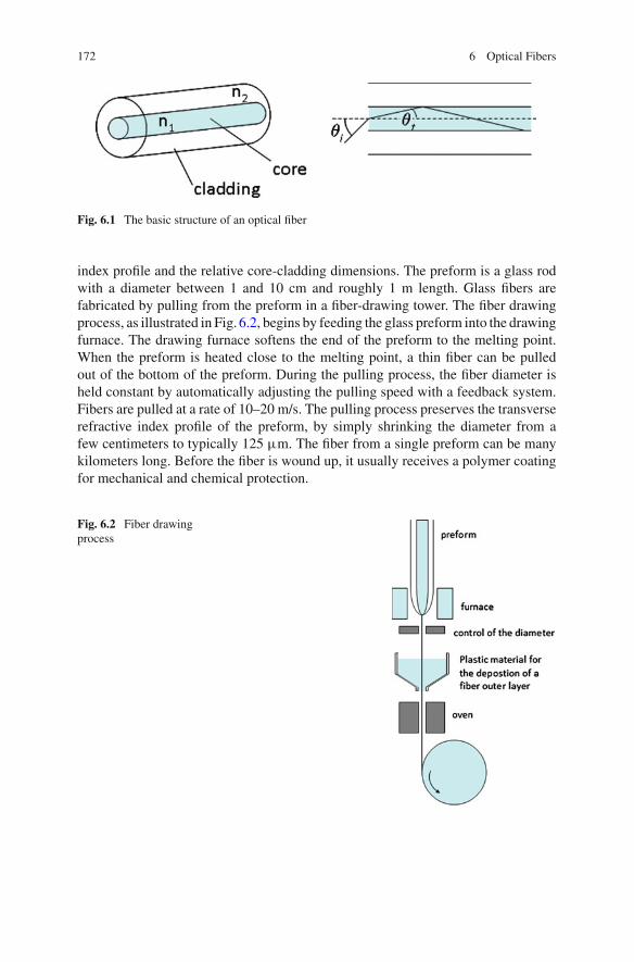
172 6 Optical Fibers
Fig. 6.1 The basic structure of an optical fiber
index profile and the relative core-cladding dimensions. The preform is a glass rodwith a diameter between 1 and 10 cm and roughly 1 m length. Glass fibers arefabricated by pulling from the preform in a fiber-drawing tower. The fiber drawingprocess, as illustrated in Fig. 6.2, begins by feeding the glass preform into the drawingfurnace. The drawing furnace softens the end of the preform to the melting point.When the preform is heated close to the melting point, a thin fiber can be pulledout of the bottom of the preform. During the pulling process, the fiber diameter isheld constant by automatically adjusting the pulling speed with a feedback system.Fibers are pulled at a rate of 10–20 m/s. The pulling process preserves the transverserefractive index profile of the preform, by simply shrinking the diameter from afew centimeters to typically 125 µm. The fiber from a single preform can be manykilometers long. Before the fiber is wound up, it usually receives a polymer coatingfor mechanical and chemical protection.
Fig. 6.2 Fiber drawingprocess

6.1 Properties of Optical Fibers 173
6.1.1 Numerical Aperture
A ray that is incident on the fiber front-face at an angle θi is refracted at an angle θt
given by the Snell’s law of (2.25):
nosinθi = n1sinθt (6.1)
where no is the refractive index of the medium in which the fiber is immersed, and n1is the refractive index of the core glass. The transmitted beam hits the core-claddinginterface at an incidence angle π/2− θt , and is totally reflected if this angle is largerthan the limit angle of arcsin(n2/n1), where n2 is the refractive index of the claddingglass. The incident ray is trapped inside the fiber if θi ≤ θmax, where the maximumacceptance angle θmax is determined by the condition:
π/2 − θt = arcsin(n2/n1) (6.2)
By using (6.1) and (6.2) it is found that θmax is given by:
sinθmax =√
n12 − n2
2
no(6.3)
The quantity nosinθmax is known as the “numerical aperture” of the fiber, usuallydesignated as N A, the same symbol used for the numerical aperture of the lens.Although the two definitions are somewhat different, the physical meaning is thesame: the numerical aperture is a measure of the light-gathering capacity of theoptical component. As an example, taking n1 = 1.48, n2 = 1.46, no = 1, one findsN A = 0.24. In this case the maximum acceptance angle is θmax = 14◦.
From now on it will be always assumed that no = 1. Sometimes it is also usefulto introduce the parameter Δ, defined as:
Δ = n12 − n2
2
2n12 ≈ n1 − n2
n1(6.4)
6.1.2 Modal Properties
The optical fiber described in the preceding section is known as a “step-index fiber”,because the refractive index profile presents an abrupt change at the core-claddinginterface. It is also possible to guide a light beam using a refractive index profilethat decreases smoothly inside the core from the center to the cladding. These fibersare known as “graded-index” fibers. Their refractive index profile can be generallyexpressed in the form:
n(r) = n2 + (n1 − n2)[1 − (r/a)γ
], (6.5)

174 6 Optical Fibers
where a is the core radius and r is the radial distance. The validity of (6.5) is limitedto the interval 0 ≤ r ≤ a. If the exponent γ tends to infinity, (6.5) reproduces astep-index profile. When γ = 2, there is a parabolic profile.
The propagation of optical waves along fibers must be treated, following the gen-eral scheme outlined in Sect. 2.6, by using the Helmholtz equation and the boundaryconditions at the core-cladding interface. Since the geometry is two-dimensional,the modes are characterized by two integer numbers, m and l. Using the cylindricalcoordinates z, r , and θ , the electric field of a generic mode, written in scalar form, isgiven by:
Elm(r, θ, z, t) = ABlm(r, θ)exp[i(βlm z − ωt)], (6.6)
where βlm is the propagation constant and Blm(r, θ) is the transverse mode profile,which is independent of the propagation distance z.
The main results of the theoretical treatment are summarized as follows. Thepropagation properties are described by a set of so-called “linearly polarized” (L Plm)modes, where an L Plm mode has m field amplitude maxima along the radial coordi-nate and 2l maxima along the circumference. The lowest order mode, i.e. the L P01mode, has a bell-shaped field amplitude distribution that is well approximated by aGaussian function:
B01(r, θ) = Boexp
(− r2
w2
), (6.7)
where w is known as the mode field radius. It has been seen in Sect. 1.4.2 that freelypropagating Gaussian waves have z-dependent parameters. In contrast, the Gaussianwave propagating inside the fiber has constant radius and a fixed planar wavefront.
While there is always a solution for the fundamental mode L P01, the existenceof higher-order modes depends on the fiber parameters. It is useful to introduce adimensionless parameter, V , known as the normalized frequency, defined as:
V = 2πa
λ
√n1
2 − n22 = 2πa
λN A. (6.8)
It can be shown that, if V is smaller than a critical value, Vc, then the fiber cansupport only the fundamental mode. In the case of a “step-index” fiber, the criticalvalue is: Vc = 2.405. In the more general case of a profile following the law (6.5),Vc is given by:
Vc = 2.405
√
1 + 2
γ. (6.9)
As an example, for γ = 2, Vc = 3.512. Above Vc the second mode, L P11, canalso propagate. As long as V increases, more and more higher-order modes canpropagate. When V � 1, the number of modes, N , that can propagate is given by

6.1 Properties of Optical Fibers 175
Fig. 6.3 Intensity of thefundamental mode plotted asa function of the ratiobetween the distance fromthe axis and the core radius,at different values of thenormalized frequency V
N = V 2
2(6.10)
At fixed fiber parameters, the condition V = Vc defines a cut-off wavelength:
λc = 2πa
Vc
√n1
2 − n22 = 2πa
VcN A. (6.11)
At wavelengths λ ≥ λc the fiber behaves as a single-mode waveguide.The intensity profile of the fundamental mode is shown in Fig. 6.3 for three values
of V . The optical power is mainly traveling inside the core, but there is also anexponential tail (the evanescent wave described in Sect. 2.2.7) extending inside thecladding. If V is larger, then the confinement inside the core ismore effective becausethen1 –n2 difference is larger. The dependence of the beam radiusw onV is describedby the empirical law:
w = a(0.65 + 1.62 V −1.5 + 2.88 V −6) (6.12)
Single-mode step-index fibers are designed by keeping the value of V close to2. Smaller values of V are avoided because the field amplitude extends increasinglyinto the cladding as V decreases. If the field amplitude is not negligible at the edgeof the cladding, then the power losses may become significant.
The single-mode condition imposes small core radius values. As an example, asingle-mode fiber, operating at λ = 1550 nm, and designed to have V = 2, can bemade by taking a/λ = 2.5 and N A = 0.12. The core radius is only 3.9 µm. Thecut-off wavelength of such a fiber is 1290 nm.

176 6 Optical Fibers
The propagation velocity of the fundamental mode is expected to be intermediatebetween the values c/n1 and c/n2, because the wave extends over both core andcladding. Its propagation constant can be written as:
β01 = 2π
λnef f , (6.13)
where the effective refractive index nef f has values in the interval n1 ≥ nef f ≥ n2.Of course, every mode has its own effective refractive index. As a general rule, if
the indices l and m are increased, then the transverse distribution is more extendedinto the cladding, and so the effective refractive index is expected to decrease.
6.2 Attenuation
The beam propagation inside the optical fiber is unavoidably lossy, so that the opticalpower decreases with the propagation distance z. Assuming linear losses, the opticalpower decays following an exponential law:
P(z) = Po exp(−αz), (6.14)
where Po is is the power launched into the fiber and α is the attenuation coefficient,already defined in Sect. 2.1. The unit commonly used to characterize loss in fibers isdecibel per kilometer (dB/km). Denoting by αo the attenuation coefficient measuredin dB/km, it is found:
αo = 10
zlog10
[Po
P(z)
]. (6.15)
If α is expressed in units of km−1, then the numerical relation between the twocoefficients is:
αo = 10 α log10e = 4.34 α (6.16)
From (6.15) it is found that the propagation distance at which the incident poweris halved, z1/2, is given by:
z1/2 = 10 log102
αo≈ 3
αo. (6.17)
As an example, if αo = 0.15 dB/km, then z1/2 = 20 km.Fiber losses are due to two effects, light scattering and absorption. Scattering
arises because there are submicroscopic random inhomogeneities in density andcomposition inside the glass, which give rise to local fluctuations in the refractiveindex. The inhomogeneities originate from thermal fluctuations in the melt of the

6.2 Attenuation 177
silica that are then frozen in, as the glass cools. Light scattering from submicroscopicscatterers, known as Rayleigh scattering, gives a wavelength-dependent attenuationcoefficient that scales as λ−4.
Silica glasses have an absorption band in the ultraviolet, due to electronic tran-sitions, and absorption bands in the mid-infrared, due to vibrational transitions. Atwavelengths greater than about 1.6 µm, absorption losses become predominant withrespect to scattering losses. The combination of scattering and absorption losses givesrise to the attenuation curve shown in Fig. 6.4, which has aminimumof≈0.15 dB/kmat about 1.55 µm. Indeed, long-distance optical communication systems use semi-conductor lasers emitting a 1.55 µm beam, as the carrier that is modulated andtransmitted through the optical fiber.
The attenuation curve of Fig. 6.4 also shows a secondaryminimumaround 1.3µm,due to the presence of an absorption peak at about 1.4 µm. This peak, due to vibra-tional transitions of theO–Hbond, occurs because of small quantities ofwater trappedinside the glass during the fiber fabrication process. This absorption peak no longerexists in recent fibers, because of improvements in the purification process. However,several networks using fibers with water impurities are still installed and in use.
Historically, the first optical-communication experiments, operating at short dis-tances, were performed at 850 nm. In optical-communication jargon, the wavelengthregion around 850 nm was called the first attenuation window. The region around1.3 µm is called the second attenuation window, and the one around 1.55 µm thethird attenuation window.
All the glasses made by different combinations of oxides offer similar infraredabsorption bands, so that the attenuation behavior shown in Fig. 6.4 is not muchchanged by varying the oxide composition. It is, however, possible to shift the vibra-tional absorption to longer wavelengths by using fluoride-based glasses instead ofoxides. The so-called “ZBLAN” glasses, made from amixture of zirconium, barium,lanthanum, aluminum, and sodium fluorides, offer attenuation minima around 3µm.
Fig. 6.4 Attenuation coefficient of a silica fiber versus wavelength

178 6 Optical Fibers
The minimum value of the attenuation coefficient is one order of magnitude lowerthan for silica glasses.
In addition to intrinsic losses, there are also fiber losses due to the departurefrom the ideal straight line configuration. In a bent fiber, the incidence angles at thecore-cladding interface change, and so the condition of total internal reflection is nolonger satisfied, meaning that the optical power is only partially trapped inside thefiber. In general, bending losses are larger for those modes that extend more intothe cladding. Typically bending losses become important when bend radii are of theorder of millimeters.
6.3 Dispersion
Optical dispersion, as defined inSect. 2.1, is related to the dependence of the refractiveindex of a material on the wavelength of the propagating beam. As discussed inSect. 6.1.2, a mode propagating in an optical fiber has an effective refractive index,which is a type of weighted average between n1 and n2. Since both materials aredispersive, one might think that the dispersion of neff is determined by that of thecore and cladding materials, to a first approximation. The situation, however, is morecomplex, because theparameterV is changedbychanging thewavelength.Therefore,the transverse field distribution is modified. As a consequence the relative weightingof n1 and n2 varies with λ. The conclusion is that the single-mode dispersion isa combination of both a material effect and a waveguide effect. The waveguidedispersion is very sensitive to the shape of the radial profile of the refractive index,such that it may significantly change on going from a step-index to a graded-indexfiber.
An intermodal dispersion occurs in multimode fibers, due to the differences ineffective refractive indices of the various modes. Even if the wavelength is the same,the differentmodes havedifferent propagation velocities.A single light pulse enteringan N -mode fiber is divided into N pulses, each traveling with a different velocity. Atthe output a broadened pulse is observed, or, for a longer propagation, a sequence ofN separated pulses.
6.3.1 Dispersive Propagation of Ultrashort Pulses
In this section, the discussion is focused on the propagation of short optical pulses insingle-mode fibers. Since a pulse can be viewed as the superposition of many waveswith different wavelengths, the fact that each wavelength travels with a differentvelocity clearly modifies the time-dependent pulse-shape. As it has been shown inSect. 3.11.3, the shorter the pulse is in time, the wider its optical spectrum. Therefore,one should expect that dispersion effects will be largest for the shortest pulses.

6.3 Dispersion 179
In order to describe pulse propagation it is useful to express the propagationconstant β(ω) = (ω/c)nef f (ω) as a power series around the central pulse frequencyωo:
β(ω) =∞∑
k=0
dkβ
dωk
(ω − ωo)k
k! , (6.18)
where the derivatives dkβ/dωk are evaluated at ωo.Assuming that the pulse spectral width, Δω, is much smaller than ωo, the power
expansion can be truncated at the quadratic term:
β(ω) = βo + β1(ω − ωo) + 1
2β2(ω − ωo)
2, (6.19)
where βo = β(ωo),
β1 = dβ
dω, (6.20)
and
β2 = d2β
dω2 . (6.21)
The electric field of the input pulse, entering the single-mode fiber at z = 0, isgiven by
E(t, 0) = A(t, 0)exp(−iωot). (6.22)
For simplicity, the term B01(r), which describes the transverse distribution of thefield amplitude and is invariant during the propagation, has been omitted.
Themathematical treatment of dispersive propagation becomes simpler if just onespecific pulse shape is considered, such as the Gaussian shape described by (3.77).This has a Fourier transform given by (3.80).
In the frequency domain, the effect of propagationmaybe regarded as a frequency-dependent phase delay, given by φ(ω, z) = β(ω)z. In this way, the Fourier transformof the field at z is simply given by:
E(ω, z) = E(ω, 0)exp[iβ(ω)z] (6.23)
By substituting (6.19) and (3.80) inside (6.23) one obtains:
E(ω, z) = √2πτi Aoexp(iβoz)exp
[−(τi
2 − iβ2z)(ω − ωo)
2
2+ iβ1z(ω − ωo)
].
(6.24)

180 6 Optical Fibers
By using (2.9), it is possible to return to the time domain, in order to recover theexpression for the time-dependent electric field at the generic coordinate z:
E(t, z) = 1
2π
∫ ∞
−∞E(ω, z)exp(−iωt)dω
= Ao√1 − iβ2z/τ 2i
exp[−i(ωot − βoz)]exp[
− (t − β1z)2(1 + iβ2z/τi2)
2τi2(1 + β2
2z2/τi4)
]
(6.25)
It is useful to separately highlight the behavior of the field amplitude and phaseby writing the electric field as:
E(t, z) = A(t, z)exp{−i[ωot − βoz + φ(t, z)]}, (6.26)
where:
A(t, z) = Ao
(1 + β22z2/τi
4)1/4exp
[− (t − β1z)2
2τi2(1 + β2
2z2/τi4)
](6.27)
and
φ(t, z) = (t − β1z)2zβ2/τi2
2τi2(1 + β2
2z2/τi4)
− arctan(β2z/τi2)
2. (6.28)
Equation (6.27) shows that the time-dependent pulse amplitude remains Gaussianduring the dispersive propagation. The pulse intensity, I (z, t), proportional to themodulus square of (6.27), reads:
I (t, z) = Io√1 + (z/L D)2
exp
[− (t − β1z)2
τi2(1 + z2/L D
2)
], (6.29)
where Io is the peak intensity of the input pulse. Equation (6.29) contains the disper-sion length L D , defined as:
L D = τi2
|β2| (6.30)
According to (6.29), the intensity observed at the coordinate z is maximum attime tp = β1z. This means that the pulse peak is propagating with a velocity, knownas the “group velocity”, which is given by:
ug = β1−1. (6.31)

6.3 Dispersion 181
The quantity β1 can be written as:
β1 = 1
c
(nef f + ω
dnef f
dω
) = ng
c, (6.32)
whereng is called group refractive index.As is the case formost transparentmaterials,the refractive index of silica glass, ngl , is an increasing function of ω. Although nef f
does not coincide with ngl , its frequency-dependence is similar, so that the derivativednef f /dω is positive. Therefore it can be quite generally said that the group velocityis smaller than the phase velocity c/nef f , according to (6.32).
Recalling that the pulse duration τp is related to τi by (3.81), the law describingthe change of pulse duration upon propagation can be derived from (6.29):
τp(z) = τp(0)
√
1 + z2
L D2 (6.33)
Equation (6.33) shows that L D represents the propagation distance above whichthere is a significant increase of the pulse duration.While the pulse spectrum remainsunchanged during propagation, the pulse duration grows with z. As a consequencethe bandwidth-duration product is no longer given by (3.81), but becomes:
Δνpτp(z) = 0.441
√
1 + z2
L D2 (6.34)
Since a lossless propagation has been considered, the pulse energy must be con-served. Indeed (6.29) shows that the intensity decreases in such a way as to keep theproduct between peak intensity and pulse duration constant during propagation.
The quantityβ2 is known as the “group velocity dispersion” (GVD) parameter, andis usually measured in units of ps2/km. At the optical-communication wavelength,λ = 1.55 µm, it is found that β2 = −20 ps2/km for a typical single-mode fiber. It isinstructive to numerically investigate the effect of pulse duration. For a 20-ps pulse,(6.30) gives L D = 20km. After a propagation length of 20km, the pulse durationis increased by a factor of
√2. For a 1-ps pulse, L D is much shorter, only 50m.
Here, the pulse duration is increased by a factor of 400, after propagating 20km.This clearly shows that the stretching effect due to dispersion plays a very importantrole for ultrashort pulses.
In the area of optical communications, it is customary to use the dispersion para-meter D, instead of β2. This is defined as:
D = dβ1
dλ= −2πcβ2
λ2(6.35)
D is measured in units of ps/(nm km). It represents the group delay per wavelength(in nm) and propagation length (in km). At λ = 1.55 µm, it is found that D =17 ps/(nm km) for a typical single-mode fiber. The so-called “normal” group-velocity
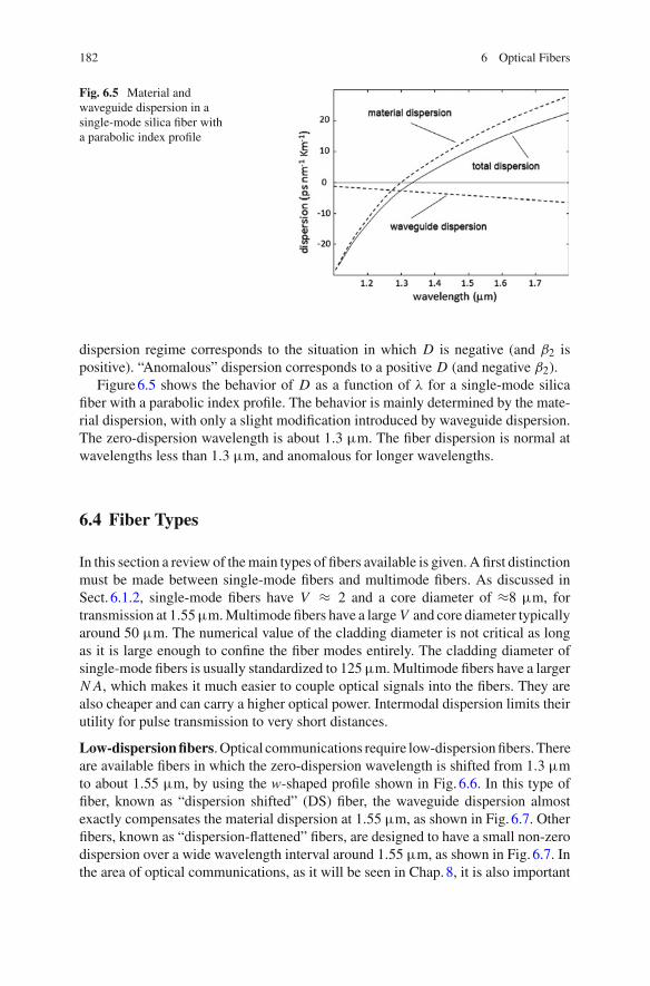
182 6 Optical Fibers
Fig. 6.5 Material andwaveguide dispersion in asingle-mode silica fiber witha parabolic index profile
dispersion regime corresponds to the situation in which D is negative (and β2 ispositive). “Anomalous” dispersion corresponds to a positive D (and negative β2).
Figure6.5 shows the behavior of D as a function of λ for a single-mode silicafiber with a parabolic index profile. The behavior is mainly determined by the mate-rial dispersion, with only a slight modification introduced by waveguide dispersion.The zero-dispersion wavelength is about 1.3 µm. The fiber dispersion is normal atwavelengths less than 1.3 µm, and anomalous for longer wavelengths.
6.4 Fiber Types
In this section a review of themain types of fibers available is given. A first distinctionmust be made between single-mode fibers and multimode fibers. As discussed inSect. 6.1.2, single-mode fibers have V ≈ 2 and a core diameter of ≈8 µm, fortransmission at 1.55µm.Multimode fibers have a large V and core diameter typicallyaround 50 µm. The numerical value of the cladding diameter is not critical as longas it is large enough to confine the fiber modes entirely. The cladding diameter ofsingle-mode fibers is usually standardized to 125µm.Multimode fibers have a largerN A, which makes it much easier to couple optical signals into the fibers. They arealso cheaper and can carry a higher optical power. Intermodal dispersion limits theirutility for pulse transmission to very short distances.
Low-dispersion fibers.Optical communications require low-dispersionfibers. Thereare available fibers in which the zero-dispersion wavelength is shifted from 1.3 µmto about 1.55 µm, by using the w-shaped profile shown in Fig. 6.6. In this type offiber, known as “dispersion shifted” (DS) fiber, the waveguide dispersion almostexactly compensates the material dispersion at 1.55 µm, as shown in Fig. 6.7. Otherfibers, known as “dispersion-flattened” fibers, are designed to have a small non-zerodispersion over a wide wavelength interval around 1.55 µm, as shown in Fig. 6.7. Inthe area of optical communications, as it will be seen in Chap. 8, it is also important

6.4 Fiber Types 183
Fig. 6.6 Refractiveindex profile in a“dispersion-shifted” fiber
Fig. 6.7 Group velocitydispersion versus λ for a“dispersion-shifted” and a“dispersion flattened” fiber
to have fibers with large normal dispersion (D ≈ −60 ps nm−1 km−1), available foruse in dispersion compensation. A short stretch of these fibers (known as “dispersioncompensating” DIS-CO) can compensate for the dispersion accumulated over a longpropagation span in an SMR fiber.
Polarization-maintaining fibers. An aspect of waveguiding that has not yet beentouched upon in this chapter is that of signal polarization. The fundamental modeL P01 is a linearly polarizedmode, but its polarizationdirection is completely arbitraryas long as the fiber has perfect cylindrical symmetry about its axis. In fact, real fibersinvariably have some slight local asymmetry, either intrinsic or due to their environ-ment, which creates a small birefringence varying randomly along their length. Asa result, the initial polarization is lost after some tens of meters, so that it becomesimpossible to predict the polarization state of the output signal. In the case of pulsepropagation, the random changes in the polarization can induce a pulse broadening.This dispersion effect, known as “polarization-mode dispersion” (PMD), is usuallysmaller than the GVD effect. For some applications it is desirable that fibers transmitlight without changing the polarization state. Such fibers are called “polarization-maintaining” fibers. One possibility is to break the cylindrical symmetry of the fiberby using an elliptical core. An alternative scheme is that of fabricating a preform that

184 6 Optical Fibers
Fig. 6.8 Polarization-maintaining fibers
Fig. 6.9 Microstructured fiber. Courtesy of NKT Photonics
contains two glass rods, inserted on the opposite sides of the fiber core, as shownin Fig. 6.8. These rods are both made of a glass that is different from the cladding,and so mechanical stress due to their different thermal expansion coefficients arisesinside the fiber structure during the cooling process. Because of stress-induced bire-fringence, the fiber becomes strongly birefringent, so that a linear polarization stateparallel to one of the principal axes is transmitted without a change in polarization.This type of fiber is sometime called “panda” fiber.
Microstructured fibers. A new family of fibers, called microstructured fibers, con-tain cylindrical air holes running parallel to the fiber axis, as shown in Fig. 6.9. Ifthe holes are organized in a regular periodic pattern, then the fiber is also calledphotonic-crystal fiber. These fibers are usually made of pure silica glass. Both thehole diameter and the minimum distance between holes are of the order of the wave-length of light.Microstructured fibers have higher losses and aremore expensive thanstandard fibers. However, they are interesting for various applications, because theirmore complicated structure gives new degrees of freedom, offering performancesnot accessible using standard fibers. Once λ is fixed, there is a very limited flexibilityregarding the choice of core diameter of standard single-mode fibers. In contrast,microstructured fibers can be designed for single mode operation with a large mode-area (mode diameter larger than 10 µm) or a very small mode-area (mode diameteraround 1 µm). Large mode-areas are interesting for transmitting high optical pow-ers, whereas small mode-areas produce intensities high enough to enhance nonlineareffects, such as the optical Kerr effect and other effects that will be described in thefollowing chapter. The dispersion properties of microstructured fibers can also be

6.4 Fiber Types 185
drastically different from those of standard fibers. In particular, the zero-dispersionwavelength can be positioned anywhere in the visible or near infrared.
Plastic optical fibers. Fibers can also be made from polymers, by using, for instancea core of polymethyl methacrylate (PMMA, n = 1.495) and a cladding of fluoroalkylmethacrylate (n = 1.402). These fibers have a transparency window in the visible,between 500 and 700 nm, have large attenuation coefficients (50–100 dB/km) andalso a large NA. They can be useful for sensors, for short-distance multimode data-transmission, and for architectural lighting.
6.5 Fiber-Optic Components
Several optical components can bemade using fibers. They are useful for themanipu-lation of optical signals that are already traveling inside fibers, so that all-fiber setupscan be realized. In this section attention is focused on two components, fiber couplersand fiber mirrors.
Couplers. Fiber couplers can couple light from one or more input fibers to one ormore output fibers. Several fibers can be thermally fused, such that their cores comeinto contact over a length of some centimeters, as shown in Fig. 6.10. When theevanescent field of one fiber reaches the core of the other fiber, a fraction, F , of thepower traveling in the first fiber is coupled into the other. An optical signal comingfrom fiber 1 can be progressively transferred to fiber 2. The power fraction that iscoupled into fiber 2 depends on the length of the coupler, L , according to the law:
F = sin2(AL), (6.36)
where the parameter A is an increasing function of λ. By varying L , fiber beam-splitters that have an arbitrary power ratio between the two output fibers can bedesigned. Fiber couplers introduce very low losses, typically 0.2–0.5 dB. Since thepower transfer depends not only on the coupling length, but also on wavelength, itis possible to design couplers, which, for instance, entirely transfer a λ1 signal fromfiber 1 to fiber 2, while leaving a λ2 signal in fiber 1. Such dichroic couplers are usedin fiber amplifiers to combine the signal input and the pump wave, as it will be seenin Sect. 6.6. Their insertion loss may be very small (below 1 dB) for both inputs.
Fig. 6.10 Scheme of a fibercoupler

186 6 Optical Fibers
In optical-communication systemswavelength-sensitive couplers are used asmul-tiplexers to combine several input signals with different wavelengths, or to separatedifferent wavelengths.
Fiber Bragg gratings. An other type of fiber component is the wavelength-selectivefiber mirror, which is conceptually similar to the multilayer mirrors discussed inSect. 2.2.4. The idea is to create a periodic change of refractive index within the core.Such a phase grating, known as “fiber Bragg grating”, has maximum reflectivitywhen the phase delay corresponding to the propagation along one period is equalto π . Therefore the wavelength of maximum reflectivity, λo, known as the Braggwavelength, is given by the relation
λo = 2mnΛ, (6.37)
where m is an integer, Λ is the periodicity of the grating and n is the refractive indexof the core.
The maximum reflectivity is calculated using the same relations (2.55) and (2.56)given in Sect. 2.2.4 for multilayer mirrors. By putting n1 = n2 = nB = n, andn A = n + Δn inside (2.56), Rmax can be expressed as:
Rmax = tanh2(
NΔn
n
), (6.38)
where N is the number of periods. The length, L , of the grating is typically of theorder of a few millimeters, and so N = L/Λ is of the order of 104. Even if Δn issmall, a maximum reflectivity very close to 100% can be obtained. As an example,taking Δn = 2 × 10⁻⁴, N = 4 × 10⁴, n = 1.5, it is found: Rmax = 99.99%. Thereflection bandwidth is typically narrower than 1 nm.
Fiber Bragg gratings are fabricated by exploiting the photosensitivity of germania-doped silica glasses to ultraviolet radiation.Radiation at awavelength around 240nm,usually coming froman excimer laser, induces a permanent change of refractive indexin the core. The increase in refractive index due to UV illumination, Δn, is small,typically about 10−4. However, this can be enhanced by forcing molecular hydrogeninto the fiber core through a high-pressure low-temperature diffusion process. Thereare variousmethods to obtain a spatially periodic illumination of the core. Themethodshown in Fig. 6.11 uses a periodic phase mask, creating interference fringes with therequired periodicity.
Fig. 6.11 Fabrication of afiber Bragg grating

6.5 Fiber-Optic Components 187
Fiber Bragg gratings are used asmirrors for fiber lasers, aswill be seen in Sect. 6.7.They also have many applications in optical communication systems and in fibersensors, as will be seen in Chap.8. A recent interesting development is that of “longperiod gratings”, in which themodulation period is larger than thewavelength. Insidethese gratings there is a wavelength-selective transfer of optical power from core tocladding. The power displaced into the cladding is ultimately dissipated, and so thegrating selectively suppresses certain wavelengths, acting as a filter.
Fiber gratings with a linear variation in the grating period (termed chirped grat-ings) are particularly useful for dispersion compensation. In these gratings, theBragg wavelength varies with position, thereby broadening the reflected spectrum.A chirped grating has the property of adding dispersion, because different wave-lengths are reflected from the grating subject to different delays. In this way, it ispossible to achieve a very large group delay dispersion, sufficient for compensatingthe dispersion of a long span of transmission fiber, in a short length of fiber grating.
6.6 Fiber Amplifiers
An optical fiber can become the active medium for optical amplification, if the fibercore is doped with rare-earth ions, such as Nd3+, Pr3+, Er3+, and Y b3+. A strongmotivation for the development of efficient fiber optical amplifiers came from thearea of optical communications. In the case of long-distance links the attenuationdue to fiber losses becomes large, and so it is necessary to periodically restore thepower level of the traveling optical signals. Fiber amplifiers offer the best physicalcompatibility with fiber transmission systems.
Amplifiers based on erbium-doped fibers, which exhibit gain over a range ofwavelengths centered on 1550 nm, were developed in the late 1980s. An importantfactor for the success of the erbium-doped fiber amplifier (EDFA) was the discov-ery that relatively high concentrations of erbium could be incorporated without ionclustering into the fiber core by co-doping with alumina.
The energy level scheme for the Er3+ ion in silica glass is presented in Fig. 6.12.By exploiting the long lifetime (about 12 ms) of the first excited level, optical gaincan be obtained for the transition between this excited level and the ground state.The system then behaves like a three-level system, similar to that of the ruby laserdescribed in Sect. 3.9. Because the ions are incorporated into a disordered solidmatrix the energy levels are considerably broadened, and so the gain is spread overa wavelength bandwidth of about 40 nm. The peak gain is obtained at 1530 nm, asshown in Fig. 6.13.
Like the solid-state lasers described in Sect. 3.9, fiber amplifiers are opticallypumped. Because of the constraints of the fiber geometry, they are longitudinallypumped, so that both pump and signal utilize the waveguiding effect of the fiber.This ensures an excellent overlap of the two waves over the entire length of thedevice, and allows the pump power to be completely absorbed and utilized.
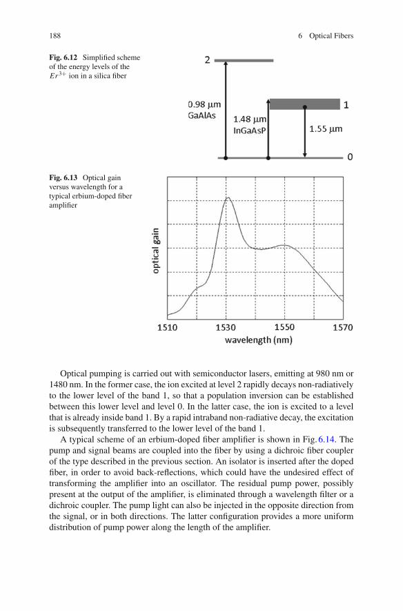
188 6 Optical Fibers
Fig. 6.12 Simplified schemeof the energy levels of theEr3+ ion in a silica fiber
Fig. 6.13 Optical gainversus wavelength for atypical erbium-doped fiberamplifier
Optical pumping is carried out with semiconductor lasers, emitting at 980 nm or1480 nm. In the former case, the ion excited at level 2 rapidly decays non-radiativelyto the lower level of the band 1, so that a population inversion can be establishedbetween this lower level and level 0. In the latter case, the ion is excited to a levelthat is already inside band 1. By a rapid intraband non-radiative decay, the excitationis subsequently transferred to the lower level of the band 1.
A typical scheme of an erbium-doped fiber amplifier is shown in Fig. 6.14. Thepump and signal beams are coupled into the fiber by using a dichroic fiber couplerof the type described in the previous section. An isolator is inserted after the dopedfiber, in order to avoid back-reflections, which could have the undesired effect oftransforming the amplifier into an oscillator. The residual pump power, possiblypresent at the output of the amplifier, is eliminated through a wavelength filter or adichroic coupler. The pump light can also be injected in the opposite direction fromthe signal, or in both directions. The latter configuration provides a more uniformdistribution of pump power along the length of the amplifier.
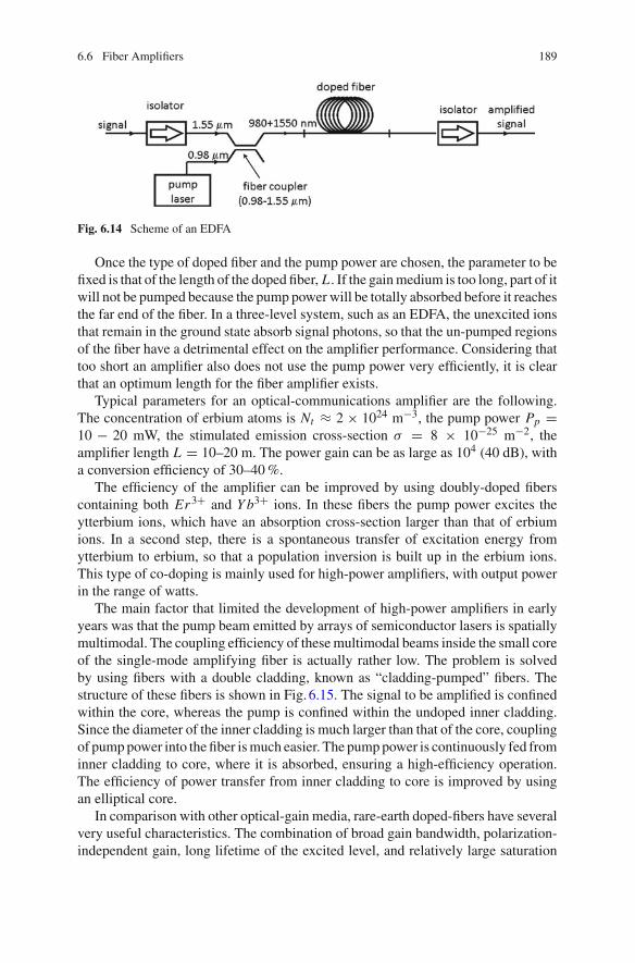
6.6 Fiber Amplifiers 189
Fig. 6.14 Scheme of an EDFA
Once the type of doped fiber and the pump power are chosen, the parameter to befixed is that of the length of the doped fiber, L . If the gainmedium is too long, part of itwill not be pumped because the pump powerwill be totally absorbed before it reachesthe far end of the fiber. In a three-level system, such as an EDFA, the unexcited ionsthat remain in the ground state absorb signal photons, so that the un-pumped regionsof the fiber have a detrimental effect on the amplifier performance. Considering thattoo short an amplifier also does not use the pump power very efficiently, it is clearthat an optimum length for the fiber amplifier exists.
Typical parameters for an optical-communications amplifier are the following.The concentration of erbium atoms is Nt ≈ 2 × 1024 m−3, the pump power Pp =10 − 20 mW, the stimulated emission cross-section σ = 8 × 10⁻²⁵ m−2, theamplifier length L = 10–20 m. The power gain can be as large as 104 (40 dB), witha conversion efficiency of 30–40%.
The efficiency of the amplifier can be improved by using doubly-doped fiberscontaining both Er3+ and Y b3+ ions. In these fibers the pump power excites theytterbium ions, which have an absorption cross-section larger than that of erbiumions. In a second step, there is a spontaneous transfer of excitation energy fromytterbium to erbium, so that a population inversion is built up in the erbium ions.This type of co-doping is mainly used for high-power amplifiers, with output powerin the range of watts.
The main factor that limited the development of high-power amplifiers in earlyyears was that the pump beam emitted by arrays of semiconductor lasers is spatiallymultimodal. The coupling efficiency of thesemultimodal beams inside the small coreof the single-mode amplifying fiber is actually rather low. The problem is solvedby using fibers with a double cladding, known as “cladding-pumped” fibers. Thestructure of these fibers is shown in Fig. 6.15. The signal to be amplified is confinedwithin the core, whereas the pump is confined within the undoped inner cladding.Since the diameter of the inner cladding is much larger than that of the core, couplingof pumppower into the fiber ismuch easier. The pumppower is continuously fed frominner cladding to core, where it is absorbed, ensuring a high-efficiency operation.The efficiency of power transfer from inner cladding to core is improved by usingan elliptical core.
In comparison with other optical-gain media, rare-earth doped-fibers have severalvery useful characteristics. The combination of broad gain bandwidth, polarization-independent gain, long lifetime of the excited level, and relatively large saturation

190 6 Optical Fibers
Fig. 6.15 Structure of a cladding-pumped optical fiber
power ensures full transparency to allmodulation formats. TheEDFAoffers the possi-bility of simultaneous amplification of multiple signals at different wavelengths (likethe multiple channels in a wavelength-division-multiplexing optical-communicationsystem). There is also a low sensitivity of the EDFA gain to pump fluctuationsoccurring on a time-scale shorter than the lifetime of the excited level τ10. Anotherimportant advantage is that the fiber geometry, with its large surface-to-volume ratio,has a good efficiency for heat dissipation.
Using schemes similar to those of EDFAs, fiber amplifiers operating at variousnear-infrared wavelengths can be made by doping silica fibers with Nd (amplifi-cation at 1.06 µ or 1.34 µm), or Y b (amplification in the range 1.05–1.12 µm).Optical amplifiers using Pr -doped ZBLAN fibers have also been tested for opera-tion in the wavelength interval 1.28–1.34 µm, where some of the existing optical-communication systems operate.
A completely different family of fiber amplifiers is represented by Raman ampli-fiers, which make use of the stimulated Raman scattering process. They will bedescribed in Chap.7.
6.7 Fiber Lasers
It is clear from the general discussion of Sect. 3.3 that the fiber amplifier can betransformed into a laser by providing an optical feedback. The initial interest in fiberlasers came from the optical-communications area, because it was thought possibleto use them as sources of high-repetition-rate pulse trains. Although the interest forsuch an application quickly vanished, fiber lasers have reached a high degree ofreliability for use in many different areas.
Fiber lasers can operate both CW and pulsed. In comparison with solid-statelasers, they have several advantages.
• When using a single-mode fiber, the output beam has a very smooth Gaussianprofile, therefore it can be focused to a very small focal spot, at variance with thebehavior of high-power semiconductor or Nd-Y AG lasers.
• The very good coupling of pump power into the fiber gives high-efficiency oper-ation.

6.7 Fiber Lasers 191
Fig. 6.16 Fiber laser schemes: a Ring cavity, b Fabry-Perot cavity
• The high surface-to-volume ratio of fiber structure provides an effective heat dis-sipation mechanism, so cooling problems are greatly simplified.
CW fiber lasers are based on Fabry-Perot cavities (see Fig. 6.16b) with mirrorsmade by fiber Bragg gratings. They use cladding pumped fibers in order to achievehigh efficiency. A particularly interesting fiber laser is the ytterbium laser. The Y b3+ion behaves like a four-level system, is pumped at 915 nm and emits in the 1000–1100 nmwavelength region. The emissionwavelength is fixed by the peak reflectanceof the FBG mirrors. The Yb-fiber laser can provide high-power outputs (up to somekilowatts). Because of its efficiency, compactness, and simplicity of cooling require-ments, it is often used in industrial processes, such asmarking, welding and precisioncutting.
Pulsed fiber lasers can be built to operate in the Q-switching regime, generatingkilohertz-frequency trains of nanosecond pulses, or in the mode-locking regime.Mode-locked fiber lasers are usually based on ring cavities (see Fig. 6.16a). Thepump beam is injected into the doped fiber by using a dichroic fiber coupler. Anotherfiber coupler is then used to extract the output beam. The mode-locking behavioris induced by inserting a modulator or a saturable absorber inside the ring. Theselasers can largely be based on telecom components, which have been developed forreliable long-termoperation andhave amoderate cost.Mode-locked erbium-dopedorytterbium-doped fiber lasers can generate trains of picosecond pulses with repetitionrates up to 20GHz. The very large gain bandwidth achievable in an ytterbium-dopedfiber is capable of supporting pulses shorter than 20 fs.
Problems
6.1 A step-index fiber has a numerical aperture of 0.15, a core refractive index of1.47 and a core diameter of 20 µm. Calculate (i) the maximum acceptance angle ofthe fiber, (ii) the refractive index of the cladding, (iii) the approximate number ofmodes with a wavelength of 800 nm that the fiber can carry.

192 6 Optical Fibers
6.2 An optical power of 10 mW is launched into an optical fiber of length 500 m.If the power emerging from the other end is 8 mW, calculate the fiber attenuation αo
in dB/km.
6.3 An erbium-doped fiber amplifier has length L = 11 m. If the stimulated-emission cross-section at λ = 1530 nm is 1.2 × 10⁻²⁰ cm2 and the populationinversion is N2 − N1 = 7 × 1017 cm−3, calculate the small-signal gain in dB units.
6.4 A light beam at λ = 1550 nm is coupled into a step-index optical fiber havingnumerical aperture N A = 0.12 and core radius a = 4.5 µm. (i) specify whether thefiber behavior will be monomodal or multimodal; (ii) calculate the parameter w ofthe fundamental mode.
6.5 A transform-limited Gaussian laser pulse having duration τp = 4 ps and angularfrequency ωo is coupled into a single-mode optical fiber. The fiber has an attenuationcoefficient αo = 0.15 dB/km and a frequency-dependent propagation constant β(ω)
following the law:
β(ω) = βo + β1(ω − ωo) + (1/2)β2(ω − ωo)2 (6.39)
where β1 = 4.90 × 10⁻⁹ s/m, β2 = −1 × 10⁻²⁷ s2/m. By assuming that the fiberlength is L = 50 km, calculate: (i) the time taken by the peak of the pulse to propagatealong the fiber; (ii) the pulse duration τp(L) at the fiber output; (iii) the ratio r betweenthe output and input energy of the laser pulse; (iv) the ratio r ′ = PL/P0, where P0and PL are the input and output peak power of the laser pulse, respectively.
6.6 Consider a step-index optical fiber with a core radius a = 4.5 µm and corerefractive index n1 = 1.494. Assuming that the normalized frequency is V = 2.15at λ = 1550 nm, calculate: (i) the cladding refractive index; (ii) the width w of thefundamental mode; (iii) the wavelength at which the fiber ceases to be single-mode.
6.7 An erbium-doped fiber amplifier has length L = 10m and a stimulated emissioncross section σ = 1.2 × 10⁻²⁰ cm2 at λ = 1550 nm. Calculate the value of thepopulation inversion N2 − N1 required to attain a small signal gain of 20 dB.
6.8 Calculate pitch and length of a fiber Bragg grating having a reflectivity peakRmax = 0.995 at λ = 1500 nm, assuming that the core average refractive index isn = 1.5 and that Δn = 2 × 10⁻⁴.
6.9 Calculate the effective refractive index nef f at λ = 1550 nm for a single-modeoptical fiber having a core radius a = 5 µm, core refractive index n1 = 1.484,cladding refractive index n2 = 1.480, by assuming that nef f = n1 f1 + n2 f2,where f1 and f2 are the power fractions traveling inside the core and the cladding,respectively. The profile of the single mode is given by the Gaussian functionexp[(x2 + y2)/w2]. The value of nef f should be given with 4 digits.
6.10 A transform-limited Gaussian laser pulse having duration τp = 1 ps is cou-pled into a single-mode optical fiber with a dispersion parameter β2 = 10 ps2/km.Calculate at which propagation distance the pulse duration is doubled.

Chapter 7Nonlinear Optics
Abstract The field of nonlinear optics ranges from fundamental studies of the inter-action of intense laser light with matter to applications such as frequency conversion,non-resonant amplification, all-optical switching. The treatment developed in thischapter restricts the attention to those topics that are of interest for applications, andlimits the notational complications to a minimum. Second-harmonic generation isdescribed in some detail in Sect. 7.2, because it is considered a case study for illus-trating the mathematical approach and the experimental methods that are generallyutilized in nonlinear optics. Section7.3 completes the description of second-ordereffects with a concise treatment of parametric amplifiers and oscillators and of sum-frequency generation. Section7.4 is devoted to a review of the main phenomenaarising from the optical Kerr effect. The subject of Sect. 7.5 is stimulated Ramanscattering, with particular emphasis on applications based on optical-fiber devices.Stimulated Brillouin scattering is described in Sect. 7.6.
7.1 Introduction
Nonlinear optics is the field of optics that considers phenomena occurring when theresponse of a medium to an applied electromagnetic field is nonlinear with respectto the amplitude of that field.
The proportionality relation between electric field and induced electric polariza-tion that was introduced in Sect. 2.1 implies that a monochromatic field oscillating atω generates a polarization P also oscillating atω. As a consequence, the propagationof a wave across a transparent medium can change the spectrum by attenuating orsuppressing some frequency component, but cannot generate new frequencies.
Nonlinear optical effects become appreciable when the displacement of chargesfrom their equilibrium position inside the material becomes so large that the induceddipole ceases to be proportional to the field amplitude E. This happens if the incidentfield amplitude is not negligible in comparisonwith the internal field Ei that holds thecharges together in thematerial. A typical value for Ei is 1011 V/m, a figure attainablewith laser fields, whereas the electric-field amplitude of conventional optical sourcescan reach at most 103 V/m. Nonlinear optics was born in the early 1960s immediatelyafter the first intense laser fields became available.
© Springer International Publishing Switzerland 2016V. Degiorgio and I. Cristiani, Photonics, Undergraduate Lecture Notes in Physics,DOI 10.1007/978-3-319-20627-1_7
193

194 7 Nonlinear Optics
The standard classification of nonlinear optical effects is based on the expansionof the electric polarization P in a series of powers of E:
P = εo(χ(1)E + χ(2)E2 + χ(3)E3 + · · · ). (7.1)
Equation (7.1) can be considered as a generalization of the linear relationexpressed by (2.11). For sake of simplicity, the notation adopted in (7.1) neglectsdispersion and uses scalar quantities.
If propagation in a medium exhibiting a non-zero χ(2) is considered, an inputfield oscillating at ω, E(t) ∝ exp(−iωt), generates a polarization component ∝χ(2) exp(−2iωt), oscillating at 2ω. Once the expression of the electric polarizationis inserted into the wave equation (2.7), the 2ω component becomes the sourceof a second-harmonic field. Analogously, if the input field contains two distinctfrequencies ω1 and ω2, then it is found that the quadratic term generates the sumfrequencyω1+ω2, and the difference frequencyω1−ω2. A similar discussion couldbe made for the cubic term. Besides optical frequency conversion, another featureof nonlinear interactions is that they can involve field-dependent modifications ofcertain material properties. This second feature opens the way to phenomena inwhich one beam can be used to control the amplitude and/or the phase of a secondbeam. To be more specific, through the optical Kerr effect a strong pump beam canchange the index of refraction of the medium in which a signal beam propagates, sothat a fully optical switch can be realized. In principle, nonlinear phenomena appearas the natural candidates for the realization of integrated all-optical devices, such asgates and logical circuits, to be used in various applications related to informationand communication technology and optical signal processing.
7.2 Second-Harmonic Generation
Consider a monochromatic plane wave having angular frequency ω and wave vectorkω propagating along the y axis inside a second-order nonlinear medium character-ized by a nonlinear susceptibility χ(2). During propagation a second-harmonic wavewill be generated, so that the total electric field of the waves traveling along y is:
E(y, t) = 1
2{Eω(y) exp[−i(ωt − kω y] + c.c.]}
+ 1
2{E2ω(y) exp[−i(2ωt − k2ω y] + c.c.]}, (7.2)
where kω = (ω/c)nω and k2ω = (2ω/c)n2ω. Here nω and n2ω are, respectively,the refractive indices experienced by the input beam, called sometimes the pumpbeam, and by the second-harmonic beam during the propagation along the nonlinearmedium.

7.2 Second-Harmonic Generation 195
Note that the field described by (7.2) is a real quantity, because of the presence ofthe complex conjugate terms. In the previous chapters many calculations have beencarried out by representing the real electric field in terms of a complex function,whose real part is the field itself. Such an approach is justified only if the real fieldand its complex representation satisfy the same propagation equations. This is trueas long as the equations are linear in the fields. The propagation equations treated inthis chapter contain nonlinear terms, and so it is mandatory to deal with real fields.
The equations describing the y-dependence of the amplitudes Eω and E2ω arederived as follows. First, by neglecting the cubic term inside (7.1), and inserting(7.2) into (7.1), an expression for P(y, t) is found. This expression will containterms oscillating at ω, 2ω, 3ω, 4ω, and also time-independent terms. Consideringonly those terms that oscillate at ω and 2ω, P(y, t) is given by:
P(y, t) = εoχ(1)
2
[Eωe−i(ωt−kω y) + c.c.] + εoχ
(1)
2
[E2ωe−i(2ωt−k2ω y) + c.c.]
+ εoχ(2)
4
[E2
ωe−2i(ωt−kω y) + c.c.] + εoχ(2)
4
[E2ω E∗
ωe−i(ωt−k2ω y+kω y) + c.c.](7.3)
As a second step, (7.2) and (7.3) are substituted inside the wave equation (2.7).By separately considering all the terms oscillating respectively as exp(−iωt) andexp(−2iωt), and further assuming that the terms containing the second-order deriv-ative with respect to y can be neglected, the following two equations are obtained:
d Eω(y)
dy= i
ωχ(2)
2cnω
E2ω E∗ω exp(iΔky), (7.4)
d E2ω(y)
dy= i
ωχ(2)
2cn2ωE2
ω exp(−iΔky), (7.5)
where Δk = k2ω − 2kω. Taking the entrance face into the medium coincident withthe plane y = 0, the initial conditions are:
Eω(0) �= 0; E2ω(0) = 0. (7.6)
Recalling that the beam intensity is related to Eω by:
Iω(y) = εonωc
2|Eω(y)|2, (7.7)
and noting that:
d Iω(y)
dy= εonωc
2
(Eω
d E∗ω
dy+ E∗
ω
d Eω
dy
), (7.8)

196 7 Nonlinear Optics
the following relation is obtained from (7.4) and (7.5):
d Iωdy
+ d I2ωdy
= 0 (7.9)
Equation (7.9) indicates that, during propagation into the lossless nonlinearmedium, there is a conservation of the overall optical power: the nonlinear mediumacts only as a catalyst, and so the second-harmonic generation (SHG) process simplyconsists of an exchange of power between the two fields.
It is not possible to find an exact analytical solution to the system of (7.4) and(7.5). However, an approximate solution is immediately found by assuming that theamplitude of the generated second-harmonic wave is so weak that the amplitudeof the fundamental wave is negligibly reduced by the SHG process. If Eω(y) isconsidered a constant, coinciding with Eω(0), then the solution of (7.5) is:
E2ω(y) = iωχ(2)
cn2ωE2
ω(0)1 − e−iΔky
iΔk(7.10)
The second-harmonic (SH) intensity is given by:
I2ω(y) = I 2ω(0)y22(ωχ(2))2
c2n2ωn2ω
4
(Δk)2sin2
(Δky
2
). (7.11)
Equation (7.11) shows that I2ω(y) is an oscillating function of y, at fixedΔk. Thismeans that there is a continuous exchange of power between pump and SH beamduring propagation. The first maximum of I2ω(y) occurs at the propagation distanceLc = π/Δk, known as the coherence length of second-harmonic generation. If thepropagation distance y exceeds Lc, the SHpower starts to decrease because the newlygenerated SH contributions have an opposite phase with respect to those generatedfor y < Lc. It is important to note that the amplitude of the spatial oscillation getsbigger and bigger as Δk decreases. Of course, if the SH power becomes large, theapproximation of no-pump-depletion is no longer applicable.
The conversion efficiency, η2ω, defined as the ratio between SH intensity at theoutput and pump intensity at the input, is expressed as:
η2ω = I2ω(L)
Iω(0)= Iω(0)L2 2(ωχ(2))2
c2n2ωn2ω
sinc2(ΔkL
2
), (7.12)
where L is the propagation length, and sinc(x) = sinx/x . The efficiency η2ω ismaximum if
Δk = k2ω − 2kω = 0, (7.13)

7.2 Second-Harmonic Generation 197
Fig. 7.1 Efficiency of thesecond-harmonic generationprocess plotted as a functionof the phase mismatch
as shown in Fig. 7.1. This condition, known as the “phase-matching” condition,implies that
n2ω = nω, (7.14)
i.e. the SH wave should travel at the same phase velocity as the pump wave, so thatall the contributions generated during propagation can add in phase.
In general terms, time-invariance and translational invariance (which meansmonochromatic plane waves interacting in an infinitely extended crystal) imposeenergy and momentum conservation among the interacting waves. Using the photonconcept, energy conservation is satisfied when two pump photons are converted intoone SH photon, andmomentum conservation requires that themomentum of the gen-erated SH photon is the sum of the momenta of the two annihilated pump photons.Therefore the phase-matching condition can be seen as a momentum conservationcondition.
By assuming Δk = 0, (7.4) and (7.5) can be exactly solved, obtaining:
I2ω(L) = Iω(0) tanh2(L/L SH ), (7.15)
and
Iω(L) = Iω(0)sech2(L/L SH ), (7.16)
where the length L SH is defined as
L SH = λ√
nωn2ω
πχ(2)Eω(0). (7.17)
It is easy to verify that I2ω(L) + Iω(L) = Iω(0) for any L . Recalling that theasymptotic limit of the hyperbolic tangent for L going to infinity is equal to 1,

198 7 Nonlinear Optics
Fig. 7.2 The second-harmonic intensity as afunction of the propagationdistance. At phase matchingI2ω asymptotically coincideswith the input intensity. Outof phase matching, I2ω is anoscillatory function
Fig. 7.3 Scheme forintracavity second-harmonicgeneration
(7.15) shows that the input intensity can be fully converted into the second-harmonicintensity, provided that the propagation distance is sufficiently long (the crystal lengthL should be much larger than LSH ). The behavior of the SH intensity as a functionof the propagation distance is illustrated in Fig. 7.2.
The first nonlinear optical experiment was performed in 1961 by Franken andcoworkers by using quartz as the nonlinear crystal. The pump was a ruby laser pulseat λ = 0.6943 µm. A very weak second-harmonic signal at λ = 0.347 µm wasdetected. In that experiment the conversion efficiency was very low, about 10−8,because the phase-matching condition was not satisfied.
SHG becomes particularly efficient if the nonlinear crystal is placed inside thelaser cavity, as schematically shown in Fig. 7.3. Intra-cavity SHG represents a veryconvenient method to generate coherent green and blue light starting from nearinfrared solid-state lasers. As an example, 532-nm green light can be generated byfrequency-doubling of a neodymium laser in a Fabry-Perot cavity in which bothmirrors are totally reflecting at 1064nm and the output mirror is totally transmittingat 532nm. Once fixed the gain in the active medium, the type of nonlinear crystal,and the cavity structure, the only free design parameter is the length L of the crystal.This is a typical optimum-coupling problem: if L is too small there is little second-harmonic generation, if L is too large there are strong cavity losses.
7.2.1 Second-Order Nonlinear Optical Materials
Similarly to the case of the Pockels effect described in Chap.4, second-order non-linear optical interactions can occur only in non-centrosymmetric materials, that
7.2 Second-Harmonic Generation 199
is, in materials that do not display inversion symmetry. Since liquids, gases, amor-phous solids (such as glass), and even many crystals do, in fact, display inversionsymmetry, χ(2) vanishes identically for such media, and consequently they cannotproduce second-order nonlinear optical interactions. Second-order optical materialsare intrinsically anisotropic, thus electric susceptibilities of any order are tensorialquantities. The i-th cartesian component of the vector P is expressed as:
Pi = εo
( 3∑
j=1
χi j E j +3∑
j,k=1
χi jk E j Ek
)(7.18)
Equation (7.18) represents an extension of the linear treatment developed inSect. 2.6 for optically anisotropic media. Assuming that the second-order tensor χi j
is diagonalized, the only non-zero components of the linear susceptibility are χ11,χ22, and χ33. Furthermore, in order to simplify the notation, only crystals possessinga symmetry axis, taken as the z-axis, will be considered. In such crystals, χ11 = χ22.
Note that (7.18) has the same structure as (4.2) that was written to describe thePockels effect, and so the properties of the third-order tensor χ(2) are similar to thoseof the electro-optic tensor, with an important difference concerning the symmetryproperties. Since the value of Pi cannot change when we exchange the position of Ek
with that of E j inside (7.18), the symmetry relation χi jk = χik j holds in this case.In the scientific and technical literature, the properties of second-order nonlinearmaterials are usually expressed in terms of the di jk tensor that is defined by:
di jk = 1
2χi jk (7.19)
In the standard notation only two indices are used, by replacing the pair jk with oneindex m running from 1 to 6. The following convention is used: m = 1 correspondsto jk = 11, m = 2 to jk = 22, m = 3 to jk = 33, m = 4 to jk = 23, m = 5 tojk = 13, and m = 6 to jk = 12. The nonlinear susceptibility tensor dim can thenbe represented as a 3 × 6 matrix.
Crystalline structures are classified according to 32 distinct symmetry classes.For each class it is possible to predict, using symmetry arguments, what tensorcomponents are non-zero. For instance, in the case of lithium niobate the non-zerocomponents are: d15, d16, d21, d22, d24, d31, d32, and d33.
In order to illustrate the basic aspects of nonlinear interactions, it is useful todiscuss some specific situations. Consider a pump beam propagating along the yaxis of a lithium niobate crystal. If the beam is an ordinary wave, linearly polarizedalong x , the index m can only take the value 1, so that, among all the non-zerocomponents of dim , the only accessible ones are d21 and d31. Since the propagationis along y, the electric polarization cannot have a longitudinal component, so d21does not play any role in the SHG process. The only surviving terms from the generalrelation (7.18) are:

200 7 Nonlinear Optics
Table 7.1 Symmetry class, transparency window and nonlinear coefficients for some nonlinearcrystals at λ = 1064nm
Crystal Class Window (µm) d (10−12 m/V)
Li NbO3 3m 0.35–5.20 d33 = 25.2, d31 = 4.6
d22 = 2.1
K T P mm2 0.35–4.50 d33 = 13.7, d31 = 6.5
d32 = 5.0
L BO mm2 0.16–2.30 d33 = 0.04, d31 = 0.85
d32 = 0.67
Lithium niobate (Li NbO3), potassium titanyl phosphate (K T i O P O4), known as KTP, lithiumtriborate (Li B3O5), known as LBO
P1(ω) = εoχ11E1(ω)
P3(2ω) = 2εod31[E1(ω)]2. (7.20)
The component P3(2ω) generates a SH field polarized along z, i.e. an extraordi-nary SH wave. Therefore the phase-matching condition becomes:
Δk = 2ω
c(ne
2ω − noω) = 0. (7.21)
If the pump beam is linearly polarized along z, the only surviving terms from thegeneral relation (7.18) are:
P3(ω) = εoχ33E3(ω)
P3(2ω) = 2εod33[E3(ω)]2 (7.22)
In this case, both pump and SH fields are extraordinary waves, and the phase-matching condition is:
Δk = 2ω
c(ne
2ω − neω) = 0. (7.23)
In order to prepare the description of the different phase-matching methods thatwill be given in the next section, it is instructive to examine the properties of somecommon nonlinear crystals—see Table7.1.
Lithium niobate and KTP exhibit large nonlinear coefficients. LBO has smallercoefficients, but its transparency window extends into the ultraviolet, and thus is thebest candidate to generate ultraviolet light by SHG.

7.2 Second-Harmonic Generation 201
7.2.2 Phase Matching
The practical importance of nonlinear optics comes from the fact that the new fieldsgenerated by nonlinear interactions can take up, in principle, all the optical power ofthe incoming fields. However, as shown in the preceding section, this is possible onlyif phase-matching is satisfied. Phase matching should be seen not only as a constraintthat limits the applicability of nonlinear effects, but also as an effective method toselect a single nonlinear interaction, from among many possible interactions. Thestructure of the equations is greatly simplified if one defines a priori which interactionwill be phase-matched. According to this criterion, only those terms relevant for SHGhave been selected in writing (7.3).
Birefringence phase matching. Since the index of refraction of anymediumchangeswith ω, it is generally not possible to satisfy the phase-matching condition (7.23).In contrast, condition (7.21) suggests the possibility of obtaining phase matchingby exploiting the crystal birefringence to compensate for material dispersion (seeFig. 7.4). As an example, lithium niobate is a uniaxial crystal presenting negativebirefringence (no > ne), as indicated in Table2.3. Taking into account that bothindices grow with ω, it can be shown that there is a frequency ωpm (corresponding toa wavelength λpm ≈ 1.1 µm), for which: no(ωpm) = ne(2ωpm). In such a situation,an ordinary input beam can be efficiently converted into an extraordinarily polarizedsecond-harmonic beam.
For a given crystal the condition no(ωpm) = ne(2ωpm) can be at most satis-fied for only one wavelength. There are, however, some degrees of freedom thatcan be exploited to obtain tunable phase matching. One possibility is offered by theconsideration that the refractive index of the extraordinary beam can be varied con-tinuously between no and ne by changing the angle between kω and the optical axis,as described by (2.128). Therefore, one can tune ωpm by rotating the crystal aroundthe axis perpendicular to the plane containing kω and the z axis. In this case there is,however, a non-zero spatial walk-off of the second-harmonic beam with respect tothe fundamental beam, because the two Poynting vectors are no longer parallel (see
Fig. 7.4 Birefringencephase matching in lithiumniobate

202 7 Nonlinear Optics
Fig. 7.5 Nonlinear crystalwith periodic inversion of theferroelectric domains
(2.129) in Chap.2). Since the spatial overlap between the two beams decreases withthe propagation distance, the walk-off effect introduces a limitation of the crystallength. Noting that the refractive indices are weakly dependent on temperature, it isalso possible to finely tune ωpm by varying T .
The method so far discussed, in which two ordinary photons at frequency ω areconverted into one extraordinary photon at frequency 2ω is known as type I phasematching. Other degrees of freedom are added to the SH experiment if two pumpbeams having the same frequency, but different directions or different polarization,are considered. A particularly interesting method, known as type I I phase matching,uses one ordinary and one extraordinary photon to generate the SH photon. Thephase-matching condition for this method is:
noω + ne
ω = 2ne2ω. (7.24)
Quasi-phase-matching. There are circumstances in which birefringence phase-matching is not suitable for an efficient SHG. For instance, the nonlinear materialmay possess insufficient birefringence to compensate for linear dispersion. Anothercase is when the application requires the use of the d33 coefficient, which is muchlarger than the off-diagonal coefficients for some crystals (see Table7.1). The d33coefficient can be accessed only if all the interacting waves have the same polariza-tion, but the problem is that the phase-matching condition (7.24) cannot be satisfiedbecause of optical dispersion. There is a method, known as quasi-phase-matching(QPM), that is alternative to birefringence phase-matching. Thismethodmakes use ofa periodically poled nonlinear crystal. As shown in Fig. 7.5, such a material consistsof a sequence of slabs parallel to the optical axis, each having a thickness Λ/2 andpresenting an alternate orientation of the optical axis. The inversion of the orientationof the optical axis does not change the index of refraction, but has the consequenceof inverting the sign of the nonlinear susceptibility, so that now d33 is not constantalong y, but exhibits a square spatial oscillation with period Λ. Considering thefirst harmonic of the function d33(y), which is expressed by the sinusoidal function(2/π)d33 exp[i(2π/Λ)y], and substituting inside (7.4) and (7.5), the phase-matchingcondition becomes:
Δk = 2ω
c(ne
2ω − neω) = 2π
Λ. (7.25)

7.2 Second-Harmonic Generation 203
Equation (7.25) implies thatΛ = 2Lc. Note that, in the case of QPM, the momen-tum of the SH photon is not equal to twice the momentum of the pump photon. Thedifference is taken up by the periodically poled crystal.
An intuitive explanation of the QPM can be given as follows. In the presenceof a wavevector mismatch, the amplitude of the generated SH wave oscillates withpropagation distance, as shown in Fig. 7.2. If the period Λ of the alternation of theoptical axis is set equal to twice Lc, then each time the SH amplitude is about tobegin to decrease because of the wavevector mismatch, a reversal of the sign of d33occurs which allows the SH amplitude to grow monotonically.
Equation (7.25) indicates that phase matching can be achieved at any desiredfrequency by appropriately choosing Λ. An important property of the periodical-poling approach to phase-matching is also that it is effective with any nonlinearcrystal, irrespective of the fact that the material might be birefringent or not. Thetechnical problem is how to fabricate a periodically poled crystal. If the nonlinearoptical material is a ferroelectric crystal, as is the case for lithium niobate and KTP,the orientation of the optical axis can be defined by a sufficiently strong static electricfield. Therefore, periodically poled structures can be fabricated by applying electricfields with a sequence of electrodes of alternating polarity. Typically, electric fieldsof the order of 20 kV/mm are applied, with a period that can be as small as 5 µm.
As an example, consider a second-harmonic-generation experiment using aneodymium laser (λ = 1064nm) and a KTP crystal. By putting 2d31 instead of χ(2)
inside (7.17), and taking d31 = 6.5pm/V, it is found that, in order to obtain a reason-able value for L SH , say 1cm, it is necessary to have an input field Eω(0) ≈ 4.7MV/m,corresponding to a laser intensity of about 5 MW/cm2. This can be obtained byfocusing the laser output or by coupling the laser beam into a nonlinear single-modewaveguide. The required intensity is however reduced by a factor 16, if QPM is usedto exploit the larger coefficient of d33 instead of d31.
7.2.3 SHG with Ultrashort Pulses
Spectral acceptance. The conversion efficiency η2ω, defined by (7.12), reduces tohalf of the peak value when ΔkL ≈ π/2, as shown in Fig. 7.1. One can there-fore define a phase-matching bandwidth Δkpm ≈ π/L , and, correspondingly, afrequency bandwidth Δωpm , usually known as the spectral acceptance. A pumpbeam at an angular frequency ω can efficiently generate a SH beam provided thatωpm − Δωpm/2 ≤ ω ≤ ωpm + Δωpm/2. The expression for Δωpm can be derivedby inserting the first-order frequency-dependence of the refractive indices into therelation
Δk = (2ω/c)ne2ω − (2ω/c)no
2ω = π/L ,

204 7 Nonlinear Optics
Fig. 7.6 Optical scheme of an autocorrelator for the measurement of duration of ultrashort pulses
and obtaining:
Δωpm = λpm
L
(dno
ω
dω− 2
dne2ω
dω
)−1
. (7.26)
The derivatives in (7.26) are calculated at ω = ωpm .The concept of spectral acceptance is very useful when dealing with nonlinear
interactions involving optical pulses. As shown in in Sect. 3.11.3, a transform-limitedpulse having a duration τp has a spectral broadeningΔωp of the order of 1/τp . All theoptical frequencies present in the pulse can contribute to SHG only ifΔωp is smallerthan Δωpm . Considering that Δωpm is inversely proportional to L , the shorter is thepulse, the smaller the crystal thickness should be.
Measurement of the duration of ultrashort pulses. The optical pulses generatedby mode-locked lasers usually have a duration much shorter than the response timeof the photodetectors (see Sect. 5.5), so it is not possible to measure their durationby direct detection. The measurement can be performed through second-harmonicgeneration by themethod illustrated in Fig. 7.6. It involves dividing the pulse into twopaths using a beam-splitter, then introducing a variable delay between the pulses, andthen spatially overlapping the two pulses in an instantaneously responding nonlinear-optical medium, such as a SHG crystal. The best performance is obtained using thetype-II phase matching described by (7.24). The linear polarization of one of thetwo pulses is rotated, so that, when they recombine at the SHG crystal, one acts asan ordinary wave and the other as an extraordinary wave. Type-II phase-matchingrequires that second-harmonic photons are exclusively generated by using one photonfrom each pulse, therefore the SH signal appears only if there is a temporal overlapbetween the two pulses. The detector response time is much longer than the pulseduration, so that the detected SH signal is an integral over time t . By sweepingthe delay τ between the two pulses, the measured SH power versus τ becomesproportional to the autocorrelation function of the pulse intensity I (t):
G(τ ) =∫ ∞
−∞I (t)I (t + τ)dt . (7.27)

7.2 Second-Harmonic Generation 205
In the case of a Gaussian pulse of duration τp, G(τ ) is also Gaussian, with a widthat half-height equal to
√2τp.
Since the delay is changed by changing the path length, and path length variationscan be controlled with an accuracy of the order of one micron, the time resolution ofthe measurement is of the order of 1 fs.
7.3 Parametric Effects
Difference-frequency generation. If twobeams at frequenciesω1 andω3,withω3 >
ω1, are sent into a second-order nonlinear crystal, then the nonlinear interactions cangive rise to new frequencies representing either the sum or the difference betweenthe input frequencies. By choosing a specific phase-matching condition, only oneprocess can be selected. In the case of difference-frequency generation (DFG), anew beam at frequency ω2 = ω3 − ω1 is generated, provided that the conditionk2 = k3 − k1 is satisfied. All the phase-matching methods discussed in the previoussection in connection with SHG can also be applied to sum/difference-frequencygeneration. If birefringence phase-matching is used, then each of the three waves canbe ordinary (o) or extraordinary (e). For instance, type I phase matching in a negativebirefringence crystal, like LBO or KTP, is described as o − o − e, indicating thatwaves atω1 andω2 are ordinary, and the highest frequencyω3 beam is extraordinary.
In the DFG process, one photon at frequency ω3 is annihilated and two photons atfrequenciesω1 andω2 are created, so that the process not only produces a new coher-ent beam at ω2, but also amplifies the beam at ω1. Such an amplification process isknown as “parametric amplification”.Whereas standard optical amplifiers work onlyat frequencies corresponding to transitions among specific energy levels, paramet-ric amplifiers use transparent crystals and can amplify, in principle, any frequencywithin the transparency window of the crystal, provided that phase matching can beachieved.
Considering collinear propagation along the y axis, the total field is given by thesuperposition of three fields:
E(y, t) = 1
2{E1(y) exp[−i(ω1t − k1y)] + c.c. + E2(y) exp[−i(ω2t − k2y)] + c.c.
+ E3(y) exp[−i(ω3t − k3y)] + c.c.} (7.28)
The nonlinear propagation equations, derived by using the same approach outlinedfor SH generation, are:
d E1(y)
dy= i
ω1χ(2)
2cn1E3E∗
2 exp(iΔky), (7.29)

206 7 Nonlinear Optics
d E2(y)
dy= i
ω2χ(2)
2cn2E3E∗
1 exp(iΔky), (7.30)
d E3(y)
dy= i
ω3χ(2)
2cn3E1E2 exp(−iΔky), (7.31)
where Δk = k3 − k1 − k2.The situation here considered is that of a high intensity ω3 beam, called pump,
and a low intensity ω1 beam, called signal. The generated ω2 beam is called idler.Equations (7.29) and (7.30) can be analytically solved at phasematching by assumingthat the pump beam is not depleted by theDFGprocess, such that E3(y) is consideredas a constant, coinciding with E3(0). Fixing the initial conditions as E1(0) �= 0 andE2(0) = 0, the obtained solutions are:
E1(y) = E1(0) cosh(gp y)
E2(y) = i
√n1ω2
n2ω1E1(0)sinh(gp y), (7.32)
where the parametric gain per unit length gp is given by:
gp = 1
2c
√ω1ω2
n1n2χ(2)E3(0). (7.33)
Equation (7.32) shows that both fields grow monotonically as functions of thepropagation distance. Since the annihilation of a photon at ω3 simultaneously pro-duces a photon at ω1 and a photon at ω2, the two intensities I1 and I2 grow in aparallel way: I1(y) = (ω1/ω2)I2(y) + I1(0). As an example, consider the case of alithium niobate crystal pumped by a 532-nm beam having an intensity of 5MW/cm2,producing a field E3(0) = 4.1 × 10⁶ V/m. Taking χ(2) = 10 pm/V, n1 = n2 = 2.2,ν1 = 3 × 10¹⁴ Hz, it is found: gp = 0.6 cm−1.
Recalling that an amplifier becomes an oscillator once a positive feedback isprovided, the parametric amplifier can be transformed into a parametric oscillatorby using an optical cavity (see Fig. 7.7). The initial seed for parametric oscillationcomes from parametric fluorescence, that is the process bywhich a “pump” photon atfrequencyω3 spontaneously breaks down into two photons at frequenciesω1 (signal)and ω2 (idler). Potentially, parametric fluorescence can yield any pair of frequenciesthat satisfy energy conservation, but the choice must also satisfy the phase-matchingcondition. Tuning of the parametric oscillator is usually achieved by rotating thecrystal or, in a finer scale, by changing the operating temperature.
Sum-frequency generation. Considering a situation in which the phase-matchingcondition is satisfied for the sum-frequency generation (SFG), and assuming againthat the pump at ω3 is not depleted, the two equations describing the evolution of thesignal field at ω1 and the sum field at ω2 = ω1 + ω3 are the following:

7.3 Parametric Effects 207
Fig. 7.7 Oscillator cavity based on parametric amplification
d E1(y)
dy= i
ω1χ(2)
2cn1E∗3 (0)E2
d E2(y)
dy= i
ω2χ(2)
2cn2E3(0)E1. (7.34)
Without loss of generality, one can put E3(0) = E∗3 (0), and the solutions are:
E1(y) = E1(0) cos(g′p y)
E2(y) = −i
√n1ω2
n2ω1E1(0)sin(g
′p y), (7.35)
where
g′p = 1
2c
√ω1ω2
n1n2χ(2)E3(0). (7.36)
The intensity conversion ratio in a crystal of length L is:
I2(L)
I1(0)= ω2
ω1sin2(g′
p L). (7.37)
In the case in which all the input ω1 photons are converted into ω2 photons, theconversion ratio has the maximum value ω2/ω1. This is larger than one, reflectingthe fact that the intensity of the converted beam is the sum of I1(0) plus the intensity(ω3/ω1)I1(0) provided by the pump beam.
SFG can be useful for converting an infrared beam into a more easily detectablevisible beam, or for generating ultraviolet light by mixing visible and infrared light.
As a final comment to this section, it should be noted that the linear electro-optic effect (Pockels effect) of Sect. 4.1 can be considered as a particular case offrequency mixing, in which the external electric field E′ at frequency ωm playsthe role of the field E1. Since ωm is negligibly small with respect to the optical

208 7 Nonlinear Optics
frequencyω, phase-matching is always satisfied in the case of the electro-optic effectfor the sum- and the difference-frequency processes, so that both frequencies ω ±ωm are generated. These frequencies are the two side-bands of the electro-opticallymodulated signal.
7.4 Third-Order Effects
Considering a centrosymmetric nonlinear material, in which the induced polariza-tion is the sum of a linear term plus a cubic term, and assuming that the material isilluminated by a monochromatic plane wave having angular frequency ω and prop-agating along the y-axis, the electric polarization inside the nonlinear medium canbe written as:
P(y, t) = εoχ(1)
2
[Eωe−i(ωt−kω y) + c.c.
] + εoχ(3)
8
[E3
ωe−3i(ωt−kω y) + c.c.]
+ 3εoχ(3)
8
[E2
ω E∗ωe−i(ωt−kω y) + c.c.
]. (7.38)
Many different nonlinear phenomena can be generated by the third-order nonlin-earity. Here the description will be limited to phenomena occurring when a singlebeam at a single frequency and direction is incident on the nonlinear medium. Wavemixing processes involving more than one incident frequency will not be discussed.
Third-harmonic generation. The electric polarization of (7.38) contains termsoscillating at ω and at 3ω. Once the expression for P(y, t) is inserted into the waveequation, the 3ω term will give rise to third-harmonic generation (THG). Formally,one could expect a behavior of the THG conversion efficiency similar to that foundfor SHG. However, the practical use of THG is rather limited because it is difficult tofind materials simultaneously having a large χ(3), a transparency window includingboth ω and 3ω, and also offering the possibility of phase matching. In practice, THGis usually obtained through a cascade of two second-order processes.
Optical Kerr effect. Neglecting the 3ω term, (7.38) can be re-written as P(y, t) =Pω exp[−i(ωt − kω y)] + c.c., where:
Pω = εo
[χ(1) + 3χ(3)
4|Eω|2
]Eω = εoχ
(1)e f f Eω, (7.39)
Equation (7.39) is similar to (4.37), which describes the Kerr effect. The bigdifference is that, in this case, the change in the susceptibility of the medium is dueto the electric field of the propagating wave, whereas, in the case treated in Sect. 4.2,the effect was induced by a “low-frequency” external field created by an electronicdevice.

7.4 Third-Order Effects 209
By using the relation between index of refraction and electric susceptibility, andassuming that the nonlinear contribution is small in comparison with the linear one,the effective refractive index is:
neff =√1 + χ
(1)eff ≈ n + n′
2|Eω|2 or neff = n + n2 I, (7.40)
where I is the intensity of the light beam and the nonlinear coefficient n2, measuredin m2/W , is given by:
n2 = 3χ(3)
4εocn2 . (7.41)
Equation (7.40) expresses the optical Kerr effect. Values of n2 are given inTable7.2 for three materials.
As already discussed for the Kerr effect in Sect. 4.2, a more detailed analysiswould show that an initially isotropic material becomes uniaxial in the presenceof a strong linearly polarized optical beam, with the direction of the optical axiscoinciding with the direction of the incident electric field. The index ellipsoid of theisotropic medium, initially spherical, acquires an intensity-dependent deformation.If the optical Kerr effect is only due to the displacement of electron clouds, theinduced birefringence almost instantaneously follows changes in the intensity of theilluminating beam. Instead of considering a self-induced effect, one could imaginea cross-induced situation, in which a high-intensity beam modulates a weak probebeam through the optical Kerr effect, with a response time as short as the durationof the pump pulse (less than 1 ps). By using the same schemes of Sect. 4.1, a veryfast amplitude- or phase-modulation could be achieved. In principle, this opens theway to the realization of all-optical modulators and switches.
It is interesting to discuss a numerical example involving the common materialof silica glass, which has χ(3) = 1.8 × 10⁻²² m2/V2, corresponding to n2 =2.4 × 10⁻²⁰ m2/W, as reported in Table7.2. A propagation along the distanceL inside the glass produces a nonlinear phase delay Δφ = (2π/λ)n2 I L . TakingL = 1 cm and λ = 1 µm, the light intensity required to induce a nonlinear phaseshift equal to π is: I = 2.1 × 10¹⁵ W/m2. Such an intensity could be reached byfocusing a laser pulse with energy of 2 µJ and a duration of 1ps into a focal spot ofdiameter 30 µm. Such an optical switch is conceptually interesting from the point
Table 7.2 Two-photon absorption and Kerr coefficients for silica glass, silicon (Si) and galliumarsenide (GaAs) at two distinct wavelengths
Material λ (nm) βa (cm/GW) n2 (cm2/W)
Silica glass 1064 2.4 × 10⁻¹⁶
Si 1540 0.8 0.45 × 10⁻¹³
GaAs 1540 10.2 1.59 × 10⁻¹³
210 7 Nonlinear Optics
of view of realizing all-optical logical circuits, but has little practical applicability,because it is bulky and requires too large a pulse energy. However, the performancecan be greatly improved by using a material with a larger n2 and confining the opticalbeams inside a waveguide of small cross-section.
Two-photon absorption. In general terms, the third-order susceptibility can be acomplex quantity, written as: χ(3) = χ
(3)Re + iχ(3)
I m . In order to see the effect of theimaginary part, consider a plane wave, with electric field (1/2)E(y) exp[−i(ωt −ky)] + c.c., propagating through a medium with a Kerr nonlinearity. The equationdescribing the evolution of the field as a function of y can be derived using the sameprocedure as that adopted for the case of the second-order nonlinearity. The result is:
d E
dy= i
ω
c3χ(3)|E |2E . (7.42)
Putting E(y) = A(y) exp[iφ(y)], where A(y) and φ(y) are real quantities, (7.42)splits into the two equations:
dφ
dy= ω
c3χ(3)
Re A2, (7.43)
and
d A
dy= −ω
c3χ(3)
I m A3, (7.44)
describing the evolution of the nonlinear phase and of the field amplitude, respec-tively. Recalling that the light intensity I is proportional to A2, and multiplying bothsides of (7.44) by 2A, it is found that I (y) satisfies the equation:
d I
dy= −βa I 2, (7.45)
where
βa = 3πχ(3)I m
εon2cλ, (7.46)
is known as the two-photon absorption coefficient. Equation (7.45) describes adecrease of intensity during propagation in an otherwise transparent medium. Thefact that the derivative of the intensity is proportional to the intensity square suggeststhat the loss is due to the simultaneous absorption of two photons. If this is the case,βa can be different from 0 only when the photon energy is larger than half the energygap between ground state and excited state.

7.4 Third-Order Effects 211
Integrating (7.45), it is found:
I (y) = Io
1 + βa Io y, (7.47)
Many experiments performed with semiconductors have indeed verified thebehavior predicted by (7.47). As an example, the values of n2 and βa for two well-known semiconductors are reported in Table7.2. Note that the energy of the incidentphoton is larger than half the bandgap energy of the two semiconductors, whereas,in the case of silica glass, the photon energy of 1.17eV is too small to give rise totwo-photon absorption.
Self-focusing. If the propagating beam has a finite cross-section, like a Gaussianspherical wave, then a new effect occurs, because the optical Kerr effect producesa transverse refractive-index profile that follows the intensity profile of the beam. Ifn2 is positive, a greater index of refraction is induced on-axis than in the wings ofthe beam, creating a positive lens that tends to focus the beam. This effect is knownas “self-focusing”. The focal length of the self-induced Kerr lens can be calculatedas follows. Assuming a radial intensity profile of the type Io exp[−2(r2/w2
o)], theradially varying refractive index is given by:
n(r) = no + n2 Io exp[−2(r2/w2o)] ≈ no + n2 Io
(1 − 2
r2
w2o
), (7.48)
where this approximate expression is obtained by expanding the exponential in apower series, and then truncating the expansion after the first order.
If the thickness of the medium is L , then the radially dependent phase delay is:
φ(r) = 2π L
λ
[no + n2 Io
(1 − 2
r2
w2o
)], (7.49)
In order to understand the effect of a transverse distribution of the phase delay,the simplest strategy is to compare (7.49) with the transverse distribution created bya real lens having focal length f . The radial dependence of the phase delay due to alens, as derived from (2.79) in Sect. 2.6, is:
φ(r) = φo −[2π
λ
r2
2 f
], (7.50)
By comparing (7.49) and (7.50), the focal length of the Kerr lens, fK , is foundto be:
fK = w2o
4Ion2L, (7.51)

212 7 Nonlinear Optics
This lensing effect has a practical application: it is used to induce self-mode-locking in solid-state lasers, such as titanium sapphire lasers. The mechanism is thefollowing. The multimode laser can operate either in a free-running regime, in whichthe modes have random phases, or in a mode-locking regime. If the number of modesis large, the peak intensity of the mode-locked pulses is much larger than the CWintensity of the free-running laser. It is assumed that the third-order nonlinearity ofthe active crystal gives rise to aKerr lens in themode-locking regime, but noKerr lensin free running. The effect of the Kerr lens is that of focusing the laser beam at somepoint inside the cavity. If a pinhole is placed at that point, the free-running regimewill experience large losses, whereas the mode-locking regime will be unaffected.As a consequence, the laser is forced to operate as a mode-locked oscillator. Moregenerally, Kerr-lensmode-locking can be explained by keeping inmind the definitionof cavity stability given in Sect. 3.8. If the cavity is designed to be stable in presenceof the Kerr lens and unstable in absence of the Kerr lens, the laser will choose tooperate in the mode-locking regime in presence of self-focusing. The technique isknown as “Kerr-lens mode-locking”.
When thematerial thickness becomes comparable to, or even larger than, fK , thenthe description of the beam propagation becomes complicated because a nonlinearwave equation needs to be solved. By increasing the input power, a situation can befound inwhich self-focusing exactly balances diffraction, and so the beampropagatesthrough the nonlinear medium without changing its profile. This phenomenon isknown as “self-trapping”. If the input power is further increased, the beam willcatastrophically focus, causing optical damage inside the medium in many cases.
Self-phase-modulation. If an optical pulse of intensity I (t) is propagating into athird-order nonlinear medium, the optical Kerr effect produces a time-dependentchange in the refractive index experienced by the same beam. This phenomenon isknown as “self-phase-modulation” (SPM). Neglecting for the moment any opticaldispersion, the phase delay over a propagation length L is given by:
φ(t) = ωot − 2π L
λo[n + n2 I (t)] (7.52)
SPM produces a broadening of the optical spectrum. The origin of broadeningcan be explained by noting that the instantaneous frequency ωinst , defined as
ωinst = dφ(t)
dt= ωo − 2π L
λon2
d I
dt, (7.53)
sweeps from a value smaller than ωo at the pulse front, where d I/dt is positive, toa value larger than ωo at the pulse tail.
In optical-communication systems, where short pulses propagate over long dis-tances inside single-mode optical fibers, it is important to account for the effect ofSPM on the pulse shape. A nonlinear equation describing the pulse evolution alongthe fiber can be derived from the wave equation by assuming that the pulse amplitudeA(y, t) is a slowly varying function of y and t (d A/dy β1A and d A/dt ωo A),

7.4 Third-Order Effects 213
and truncating to the second order the power series expansion of the propagationconstant β, as expressed in (6.19). The nonlinear equation obtained is then:
∂ A
∂y+ β1
∂ A
∂t+ 1
2iβ2
∂2A
∂t2= iγ |A|2A, (7.54)
where γ is a constant proportional to n2:
γ = n2ωo
cAef f, (7.55)
and Aeff is the mode area. A typical value in the case of a single-mode silica fiber is:γ = 2 W−1km−1.
In general the combined effect of dispersion and nonlinearity is for a broadening ofthe pulse both in time and frequency. However, if β2 and n2 have opposite signs, as isthe case for a nonlinearmedium exhibiting positive n2 and anomalous group-velocitydispersion, it is possible to find a situation in which the two effects compensate eachother. A pulse that can propagate unchanged is known as a temporal optical soliton,and has the form:
As(y, t) = Asosech
(t − β1y
τs
)expiκy . (7.56)
Equation (7.56) describes a pulse traveling at the group velocity β1−1, with a peak
amplitude Aso and a duration τs that are mutually connected by the relation
Asoτs =√
|β2|γ
, (7.57)
and κ is given by:
κ = |β2|2τs
2 . (7.58)
Note that the pulse duration τs can take any value, but the shorter the pulse thehigher the peak intensity should be, according to (7.57). The pulse energy required,which is proportional to A2
soτs , is inversely proportional to the pulse duration.In principle, the pulse described by (7.56) could propagate without distortion for
an arbitrary propagation length, and so could be of great interest for long-distanceoptical communications. However, the presence of effects that have been neglectedin the derivation of (7.54), such as fiber losses and third-order dispersion, stronglydiminishes the practical applications of solitons.

214 7 Nonlinear Optics
7.5 Stimulated Raman Scattering
When a light beam at frequency νp travels across a transparent medium, a usuallysmall fraction of its power is scattered in all directions because of the presence ofthermal fluctuations inside the medium. In addition to the main Rayleigh scatteringcontribution at νp, the spectrum of scattered light may also contain a much weakercontribution at the down-shifted frequency νst = νp − νv, where νv is the frequencyof a vibrational mode of the medium. This secondary process is known as “Ramanscattering”. The energy difference between the incident photon and the Raman scat-tered photon is used to excite a molecular vibration. The phenomenon occurs inmolecular gases and liquids, and also in amorphous or crystalline solids. In the caseof gases, Raman scattering can occur also in connection with molecular rotationallevels.
Besides scattering events in which vibrational energy is transferred to the mole-cule, usually called Stokes processes, there are also events in which vibrationalenergy is taken from the molecule. This may happen if the molecule is already in anexcited vibrational state. For these anti-Stokes processes, the Raman scattering eventde-excites the molecule, and so the scattered photon has a frequency νast = νp + νv
(see Fig. 7.8). The number of anti-Stokes scattering events is smaller than that ofStokes scattering events because the number of excited molecules is smaller thanthat of non-excited ones. At thermal equilibrium, the ratio between the anti-Stokesand the Stokes intensity is given by:
Iast
Ist=
(νast
νst
)4exp
(− hνv
kB T
). (7.59)
Since, typically, hνv is of the order of 0.1 eV, whereas kB T = 0.025 eV at roomtemperature, spontaneous Raman scattering is dominated by Stokes emission.
Fig. 7.8 Raman emission

7.5 Stimulated Raman Scattering 215
Fig. 7.9 Raman shift insilica glass
In the case of spontaneous Raman scattering, the Stokes photon is emitted witha random direction and a random phase. If the medium is simultaneously illumi-nated by a pump beam at frequency νp and a second beam at the Stokes frequencyνst = νp − νv, then there is a finite probability that a stimulated Raman scattering(SRS) process occurs, where the scattered Stokes photon is emitted with the samek-vector and the same phase of the incident Stokes photon. The stimulated processabsorbs one photon from the pump, adds one photon to the Stokes field and, at thesame time, excites a molecular vibration. Therefore, stimulated Raman scatteringamplifies the field at νst at the expense of the pump power. Note that such an ampli-fication method can be applied to beams of any frequency. In fact, provided thatthe medium is transparent to both pump and Stokes frequencies, it is not requiredthat νp and νst be coincident with internal resonances of the atomic system, as isrequired for a standard light amplifier. To obtain Raman gain the pump field and theStokes field need not necessarily be collinear, but the maximum effect is obtainedin the collinear configuration, considering that the experiments are performed withGaussian beams of finite transversal size. In the following, the discussion is limitedto SRS processes occurring in single-mode optical fibers, where propagation of thetwo fields is necessarily collinear.
Fiber Raman amplifier. In the case of silica glass, Raman scattering offers a broadspectrum (see Fig. 7.9) centered around a shift of 13 THz, instead of a sharp line. Thisshift corresponds to the vibrational frequency of the Si–O bond. The Raman peak isbroadened because glass is a disordered medium, and so the vibrational frequency ofthe Si–O bond is somewhat dependent on the random local environment. Assumingthat a strong pump wave at frequency νp and a weak Stokes wave at a frequencyνst ≈ νp − 13 THz are launched into the fiber, the Stokes wave gets amplifiedthrough SRS. Since both pump wave and Stokes wave will be fiber modes, theirtransversal distribution is fixed during propagation (no diffraction!). Consequently,only the dependence of the field amplitudes on the propagation distance y has to beconsidered. The equation describing the evolution of the Stokes field is:
216 7 Nonlinear Optics
d Est
dy= i
3ωst
cnsχ(3)E∗
p E p Est − α
2Est , (7.60)
whereα is the loss coefficient. It is evident from the structure of the gain term in (7.60)that stimulated Raman scattering is a third-order nonlinear process. A very importantproperty of SRS is that phase-matching is always satisfied because the momentumdifference between incident and scattered photon is taken up by the medium.
The equation describing the propagation of the optical power, Pst , as derived from(7.60), is the following:
d Pst
dy= gR
Aef fPp Pst − αPst , (7.61)
where Pp is the pump power, Aeff the area of the fiber mode, and gR the Raman-gaincoefficient, defined by:
gR = 12ωst n p
εoc2nstχ
(3)I m . (7.62)
Note that the Raman gain depends on the imaginary part of χ(3). This is notsurprising because processes in which there is an exchange of energy between waveand medium generally depend on the imaginary part of the electric susceptibility, ashas already been seen in the case of two-photon absorption.
Assuming no pump-depletion, i.e. a constant Pp, the integration of (7.61) givesthe Raman gain in a fiber of length L:
G = exp
[(gR
AeffPp − α
)L
](7.63)
For instance, at λ = 1.55 µm, taking gR/Aeff = 3.2 × 10⁻³ m−1W−1, Pp = 2 W,αo = 0.2 dB/km, which means α = 0.46 × 10⁻⁴ m−1, L = 500m, it is found aRaman gain of about 25. Signal amplification by SRS is commonly used in opticalcommunication links.
So far only stationary beams have been considered. What happens with shortpulses? It is found that the Raman gain has a build-up time that is related to thespontaneous decay time of molecular vibrations. The precise value depends on thespecific vibrational transition, but a typical value is ≈1ps. Therefore, for pulsesshorter than about 1 ps, the Raman gain becomes smaller and is essentially negligiblefor femtosecond pulses.
If only the pump beam is present at the fiber input, then spontaneous Raman scat-tering provides a weak signal that can act as a seed for growth of the Stokes wave.If the first Stokes wave becomes sufficiently powerful, then it can in turn generatethe second Stokes, and so on. As a consequence, a large fraction of the input powercan be transferred to the Raman lines. Furthermore, it should be noted that stimu-lated Raman scattering may be either forward- or backward-propagating in the fiber.
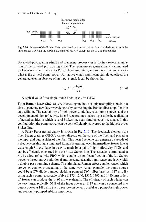
7.5 Stimulated Raman Scattering 217
Fig. 7.10 Scheme of the Raman fiber laser based on a nested cavity. In a laser designed to emit thethird Stokes wave, all the FBGs have high reflectivity, except for the λs3 output coupler
Backward-propagating stimulated scattering process can result in a severe attenua-tion of the forward propagating wave. The spontaneous generation of a stimulatedStokes wave is detrimental for Raman fiber amplifiers, and so it is important to knowwhat is the critical pump power, Pcr , above which significant stimulated effects aregenerated even in absence of an input signal. It can be shown that
Pcr ≈ 16Aeff α
gR. (7.64)
A typical value for a single-mode fiber is: Pcr ≈ 1.5W.
Fiber Raman laser. SRS is a very interestingmethod not only to amplify signals, butalso to generate new laser wavelengths by converting the Raman fiber amplifier intoan oscillator. The availability of high-power diode lasers as pump sources and thedevelopment of high reflectivity fiber Bragg gratingsmakes it possible the realizationof nested cavities in which several Stokes lines can simultaneously resonate. In thisconfiguration the pump power can be very efficiently converted to the highest-orderStokes line.
A Fabry-Perot nested cavity is shown in Fig. 7.10. The feedback elements arefiber Bragg gratings (FBGs), written directly on the core of the fiber, and placed atthe input and output sides of the fiber. This nested scheme can generate a cascade ofn frequencies through stimulated Raman scattering: each intermediate Stokes line atwavelength λsk oscillates in a cavity made by a pair of high-reflectivity FBGs, andcan be efficiently converted into the λsk+1 Stokes line. The cascade is terminated atλsn by a low-reflectivity FBG, which couples a significant fraction of the λsn Stokespower to the output. An additional grating centered at the pumpwavelengthωp yieldsa double-pass pumping scheme. The stimulated Raman effect couples waves whichare co- or counter-propagating in the same way. As an example, the pump sourcecould be a CW diode-pumped cladding-pumped Y b3+ fiber laser at 1117 nm. Byusing such a pump, a cascade of five (1175, 1240, 1315, 1395 and 1480 nm) ordersof Stokes can produce the 1480 nm wavelength. The efficiency of such a laser canbe very large: typically 50% of the input power at 1117 nm can be converted intooutput power at 1480 nm. Such a source can be very useful as a pump for high-powerand remotely-pumped erbium amplifiers.

218 7 Nonlinear Optics
7.6 Stimulated Brillouin Scattering
In a dense medium another effect of thermal fluctuations is to generate spontaneousacousticwaves oscillating at all possible frequencies andpropagating in all directions.As has been described in Chap.4, the interaction between an optical wave and anacoustic wavemay give rise to a frequency-shifted diffracted wave. The phenomenonby which an incident beam is diffracted by a randomly excited acoustic wave insidecondensed matter is known as Brillouin scattering.
Considering a plane wave with frequency νi and wave vector ki incident on themedium, Brillouin scattering is observed in all possible direction. Selecting lightscattered at an angle α with respect to the direction of ki, the observed spectrum ofthe scattered light is found to contain three peaks, one at νi and two at the frequenciesνi ± νs , where νs is the frequency of the spontaneous acoustic wave that produces adiffracted beam in the chosen direction. Taking kd as the wave vector of the photondiffracted at angle α, then the wave vector ks of the acoustic wave involved in theprocess is given by (4.43) (see also Fig. 4.12). The peaks at the frequencies νi ± νs
are both found in the spectrum because both orientations of ks are present inside themedium. The modulus of ks is derived from (4.40), taking into account that the angleθ of (4.40) coincides with α/2. The corresponding acoustic frequency is:
νs = ks
2πus= ki
πussin(α/2) (7.65)
Similarly to the case of SRS, it is possible to have stimulated Brillouin scattering(SBS) at the frequency νi − νs . The SBS wave is usually observed in the backwarddirection (α = π ), because the maximum overlap between the incident and thescattered wave occurs for that direction. In the forward direction ks = 0, so therecan be no Brillouin shift.
While the material nonlinearity of silica is actually not very high, the small effec-tive mode area and long propagation length used in fibers tend to strongly favornonlinear effects. For silica fibers, the Brillouin frequency shift is of the order of10− 20 GHz. The dependence of the Brillouin frequency shift on the material com-position and, to some extent, on the temperature and pressure of the medium can beexploited for fiber-optic sensors.
If only the pump beam is present, then spontaneous Brillouin scattering providesa weak signal at νi − νs that can act as a seed for growth of a stimulated Brillouinscatteringwave. Inside optical fibers the spontaneous generation of SBS is frequentlyencountered when narrow-band optical signals (e.g. from a single-frequency laser)are amplified in a fiber amplifier, or have just propagated through a passive fiber.This effect is usually undesirable, and so the optical setup is designed to avoid thegeneration and propagation of SBS.

Problems 219
Problems
7.1 The frequency of a Nd-YAG laser output (λ = 1064 nm) is to be doubled ina lithium niobate crystal by type-I birefringence phase matching. Knowing that, forLi NbO3, no(λ = 1064 nm) = 2.2347, ne(λ = 532 nm) = 2.2316, and no(λ =532 nm) = 2.3301, calculate the phase-matching angle between the optical axis andthe direction of the incoming beam.
7.2 Calculate the second-harmonic conversion efficiency for type-I harmonic gen-eration in a perfectly phase-matched 2-cm long KTP crystal with an incident beamat λ = 1064 nm having an intensity of 3 MW/cm2. (For KTP, nω = n2ω ≈ 1.8, andχ(2) = 13pm/V).
7.3 The generation of the second-harmonic of 1064-nm light is performed by usinga periodically poled lithium niobate crystal (ne = 2.1550 at λ = 1064 nm andne = 2.2316 at λ = 532 nm). Calculate the period of periodical poling required forphase matching of second-harmonic generation.
7.4 A parametric amplifier uses a 2-cm long KTP crystal (n1 ≈ n2 ≈ 1.77, χ(2) =10 pm/V) to amplify light of wavelength 580 nm in a collinear wave configuration.The pump wavelength is λ = 400 nm and its intensity is 4 MW/cm2. Determine thegain coefficient and the overall gain.
7.5 A Q-switched Nd-YAG laser produces an output pulse containing 10 mJ ofenergy with a pulse duration of 10 ns. The pulse generates an optical Kerr effectin a 2-cm thick carbon disulfide (n2 = 3.2 × 10⁻¹⁴ cm2/W) cell. Assuming thatwo = 100 µm, calculate the focal length due to the self-focusing effect.
7.6 A 1540-nm 2-ns laser pulse impinges on a 1-mm thick GaAs plate. Assuminga spot size of 0.2 mm and a two-photon absorption coefficient βa = 10.2 cm/GW,calculate the transmittance of the plate for the two cases in which the pulse energyis 1 mJ and 100 µJ.
7.7 A laser pulse at λo = 1064 nmpropagating into an optical fiber excites a cascadeof stimulated Raman scattering processes. Assuming that the Raman frequency shiftis 13 THz, calculate the wavelength of the second Raman Stokes line, λs2.

Chapter 8Applications
Abstract This chapter concisely describes the most important applications of pho-tonics, which are based on the optical methods and devices discussed in Chaps. 1–7.Section8.1 deals with the applications to information and communication technol-ogy. After introducing the design principles of digital information transmission andrecording, the structure and properties of an optical communication link are pre-sented. This is followed by a description of optical memories and of the prospectsof integrated photonics. Section8.2 is dedicated to optical metrology and sensing,including the optical radar, the laser gyroscope, and fiber-optic sensing of temper-ature, strain, and electric current. The achievements and the potentialities of lasermaterials processing are reviewed in Sect. 8.3, with some examples of the manypossible biomedical applications treated in Sect. 8.4. The last three sections concerntopics of very wide interest, with an impact on everyday life: displays, lighting andphotovoltaic energy conversion. In all of these, photonic methods and devices playan increasingly important role, even if lasers are not directly involved.
8.1 Information and Communication Technology
Photonics pervades all the aspects of the information and communication technol-ogy. Optical-fiber transmission of data, voice, and video is the basic technology forlong-haul communications and internet traffic, and is now also reaching individualusers directly via fiber-to-the-home broadband networks. Optical discs are used fordistributing digitally encoded music and films, and for storing large amounts of data.Printing and photocopying machines rely on lasers. High-speed data processing willbenefit from the development of integrated photonic circuits in the near future.
Before describing specific applications, it is useful to discuss some general aspectsconcerning digital information recording and transmission.
A written text is a combination of alphabetical and mathematical symbols. Eachsymbol is identified by a sequence of 7 binary units, known as bits, allowing 27 = 128combinations (ASCII code). As an example, a page of 2000 characters correspondsto a sequence of 14000 bits, that is, 14 kb.
© Springer International Publishing Switzerland 2016V. Degiorgio and I. Cristiani, Photonics, Undergraduate Lecture Notes in Physics,DOI 10.1007/978-3-319-20627-1_8
221
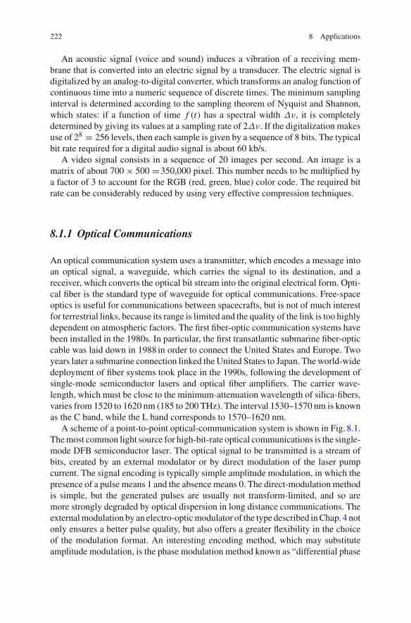
222 8 Applications
An acoustic signal (voice and sound) induces a vibration of a receiving mem-brane that is converted into an electric signal by a transducer. The electric signal isdigitalized by an analog-to-digital converter, which transforms an analog function ofcontinuous time into a numeric sequence of discrete times. The minimum samplinginterval is determined according to the sampling theorem of Nyquist and Shannon,which states: if a function of time f (t) has a spectral width Δν, it is completelydetermined by giving its values at a sampling rate of 2Δν. If the digitalization makesuse of 28 = 256 levels, then each sample is given by a sequence of 8 bits. The typicalbit rate required for a digital audio signal is about 60 kb/s.
A video signal consists in a sequence of 20 images per second. An image is amatrix of about 700 × 500 =350,000 pixel. This number needs to be multiplied bya factor of 3 to account for the RGB (red, green, blue) color code. The required bitrate can be considerably reduced by using very effective compression techniques.
8.1.1 Optical Communications
An optical communication system uses a transmitter, which encodes a message intoan optical signal, a waveguide, which carries the signal to its destination, and areceiver, which converts the optical bit stream into the original electrical form. Opti-cal fiber is the standard type of waveguide for optical communications. Free-spaceoptics is useful for communications between spacecrafts, but is not of much interestfor terrestrial links, because its range is limited and the quality of the link is too highlydependent on atmospheric factors. The first fiber-optic communication systems havebeen installed in the 1980s. In particular, the first transatlantic submarine fiber-opticcable was laid down in 1988 in order to connect the United States and Europe. Twoyears later a submarine connection linked the United States to Japan. Theworld-widedeployment of fiber systems took place in the 1990s, following the development ofsingle-mode semiconductor lasers and optical fiber amplifiers. The carrier wave-length, which must be close to the minimum-attenuation wavelength of silica-fibers,varies from 1520 to 1620 nm (185 to 200 THz). The interval 1530–1570 nm is knownas the C band, while the L band corresponds to 1570–1620 nm.
A scheme of a point-to-point optical-communication system is shown in Fig. 8.1.Themost common light source for high-bit-rate optical communications is the single-mode DFB semiconductor laser. The optical signal to be transmitted is a stream ofbits, created by an external modulator or by direct modulation of the laser pumpcurrent. The signal encoding is typically simple amplitude modulation, in which thepresence of a pulse means 1 and the absence means 0. The direct-modulation methodis simple, but the generated pulses are usually not transform-limited, and so aremore strongly degraded by optical dispersion in long distance communications. Theexternalmodulation by an electro-opticmodulator of the type described inChap. 4 notonly ensures a better pulse quality, but also offers a greater flexibility in the choiceof the modulation format. An interesting encoding method, which may substituteamplitude modulation, is the phase modulation method known as “differential phase
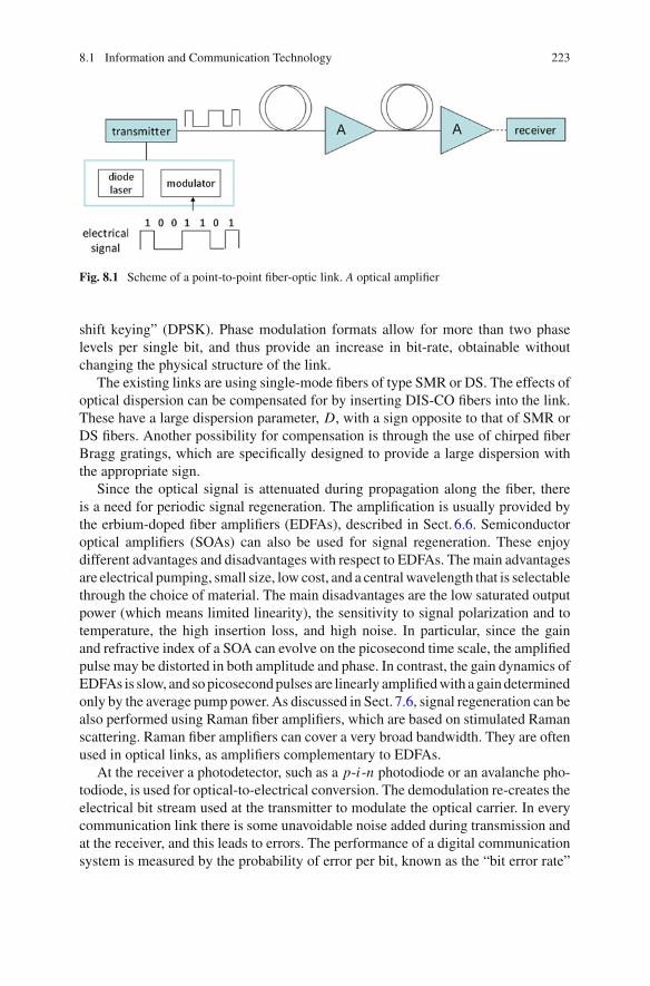
8.1 Information and Communication Technology 223
Fig. 8.1 Scheme of a point-to-point fiber-optic link. A optical amplifier
shift keying” (DPSK). Phase modulation formats allow for more than two phaselevels per single bit, and thus provide an increase in bit-rate, obtainable withoutchanging the physical structure of the link.
The existing links are using single-mode fibers of type SMR or DS. The effects ofoptical dispersion can be compensated for by inserting DIS-CO fibers into the link.These have a large dispersion parameter, D, with a sign opposite to that of SMR orDS fibers. Another possibility for compensation is through the use of chirped fiberBragg gratings, which are specifically designed to provide a large dispersion withthe appropriate sign.
Since the optical signal is attenuated during propagation along the fiber, thereis a need for periodic signal regeneration. The amplification is usually provided bythe erbium-doped fiber amplifiers (EDFAs), described in Sect. 6.6. Semiconductoroptical amplifiers (SOAs) can also be used for signal regeneration. These enjoydifferent advantages and disadvantages with respect to EDFAs. The main advantagesare electrical pumping, small size, low cost, and a centralwavelength that is selectablethrough the choice of material. The main disadvantages are the low saturated outputpower (which means limited linearity), the sensitivity to signal polarization and totemperature, the high insertion loss, and high noise. In particular, since the gainand refractive index of a SOA can evolve on the picosecond time scale, the amplifiedpulse may be distorted in both amplitude and phase. In contrast, the gain dynamics ofEDFAs is slow, and sopicosecondpulses are linearly amplifiedwith againdeterminedonly by the average pump power. As discussed in Sect. 7.6, signal regeneration can bealso performed using Raman fiber amplifiers, which are based on stimulated Ramanscattering. Raman fiber amplifiers can cover a very broad bandwidth. They are oftenused in optical links, as amplifiers complementary to EDFAs.
At the receiver a photodetector, such as a p-i-n photodiode or an avalanche pho-todiode, is used for optical-to-electrical conversion. The demodulation re-creates theelectrical bit stream used at the transmitter to modulate the optical carrier. In everycommunication link there is some unavoidable noise added during transmission andat the receiver, and this leads to errors. The performance of a digital communicationsystem is measured by the probability of error per bit, known as the “bit error rate”

224 8 Applications
Fig. 8.2 Wavelength division multiplexing technique
(BER). The BER is required to be <10−9, which means one wrong bit every billionbits. All receivers need a certain minimum power to operate reliably. This powerlevel is known as the receiver sensitivity.
One way of increasing the transmission bandwidth of an optical link is to employthe technique of “wavelength divisionmultiplexing” (WDM). In this scheme, signalswith different carrier wavelengths are mixed together (i.e. multiplexed) and thentransmitted simultaneously down a fiber, according to the scheme shown in Fig. 8.2.This technique increases the capacity of an optical fiber system without changingthe fiber and without increasing the bit rate in the single carrier. In order to minimizecross-talk, the frequency separation between two adjacent carriers (called “channels”in the optical-communication jargon)must be greater than themodulation bandwidthused by a single channel. A typical situation is that of a 40-channel WDM system,using 40 lasers, all operating in the C band, with a wavelength spacing of 0.8 nm(corresponding to a frequency spacing of 100 GHz). If the bit rate of each channelis kept around 10 Gb/s, then interference among different channels is negligible.This system has the same capacity of a single channel that transmits at 400 Gb/s. Atpresent, WDM systems with a capacity of several Tb/s are available. WDM can playan important role in a network where a number of users are connected to a centralhub. Each user is assigned a particular transmission wavelength. The individualwavelength required by each user is isolated by using a narrow-band optical filter.
8.1.2 Optical Memories
In an optical memory, data are stored in a digital format on an optical disc, and can beread-out by a laser beam. An optical disc is a flat circular disc on which binary data(bits) are encoded in the form of pits (binary value of 0, due to lack of reflection whenread) and lands (binary value of 1, due to a reflection when read) on a special materialon one of its flat surfaces. The diameter of a single pixel and the pixel separationare about 1 µm. A laser source writes one bit of data at a time on the disc, typicallythrough a thermal mechanism. The pixels are written along a spiral developing froman inner radius to an outer radius.
8.1 Information and Communication Technology 225
A variety of different materials and recording mechanisms can be used. Bothwrite-once read-many (WORM) and magneto-optic read/write discs are presentlyavailable. In the case ofWORMdiscs, a focused laser beamheats a spot on the surfacelayer during the recording stage. The local reflectance of the surface is irreversiblychanged, either by creating a pit or by modifying the surface properties. In the caseof the read/write disc, light absorption reversibly transforms the crystalline structureof the surface layer (typically made by the AgInSbTe or GeSbTe compounds) toproduce a large difference in reflectivity through a phase transition. If the material ismagneto-optic, such as some rare-earth transition-metal alloys of TbFeCo, the effectof the phase transition is to rotate the polarization of reflected light. The rotation isdetected by crossed polarizers.
The first generation of the compact discs (CDs), developed in themid-1980s, weredesigned to hold up to 75min of music which required 650 Mb of storage.
Optical discs are usually between 7.6 and 30 cm in diameter, with 12 cm beingthe most common size. A typical disc is about 1.2 mm thick, while the track pitch(distance from the center of one track to the center of the next) is typically 1.6 µm.
Optical discs are most commonly used for storing music (e.g. for use in a CDplayer), video (e.g. for use in a Blu-ray player), or data and programs for personalcomputers. For computer data backup and physical data transfer, optical discs aregradually being replaced with faster, smaller solid-state devices, especially the USBflash drive.
The objectives used to focus the light beams are characterized by their numericalaperture (NA), defined in Sect. 2.2.9. When a light beam is focused by an objectivewith a given NA, the diameter of the obtained focal spot is:
d f = aλ
NA, (8.1)
where a is a numerical constant of the order of 1. The area used to record one bit ofinformation is 2d f
2. If λ = 0.8 µm, it is possible to memorize 150 Mb over 1 cm2.The basic digital memory unit is the byte (B), which is equivalent to 8 bit. To givean example of the used notation: 106 Byte = 1 MegaByte = 1MB.
An important technical aspect concerning the design of optical disc readers is thatthe distance between lens and disc surfacemust remain constant towithin an accuracyof the order of the Rayleigh length (a few microns). This requires a sophisticatedreal-time active stabilization system.
The most common optical discs have the following properties.
Compact Disc. A Compact Disc (CD) uses a GaAlAs semiconductor laser, emittinginfrared light of 780 nm, for writing and reading. The laser beam is focused with anobjective that has a NA=0.45–0.50. The size of the focal spot on the disc surface is1.6 µm. The CD capacity is of 680 MB.
Digital Versatile Disc. ADigital VersatileDisc (DVD) uses aGaAlAs semiconductorlaser, emitting red light of 650 nm, for writing and reading. The laser beam is focusedwith an objective that has a NA=0.60–0.65. The size of the focal spot on the disc

226 8 Applications
surface is 1.1µm. The DVD capacity is of 4.7 GB, and can be doubled by using bothdisc surfaces.
Blu-Ray. A Blu-Ray disc uses a GaI nN semiconductor laser, emitting light of405 nm (notwithstanding the name of the disc, this is violet light!), for writing andreading. The laser beam is focused with an objective that has a NA = 0.85. The sizeof the focal spot on the disc surface is 0.48 µm. The DVD capacity is of 25 GB, andcan be doubled by using both disc surfaces.
The capacity of optical memories could be significantly increased by using “vol-ume” storage instead of “surface” storage. Such a possibility is actively being inves-tigated, but, at present, no commercial products are available.
8.1.3 Integrated Photonics
Optical systems, as they have been described throughout this book, contain vari-ous discrete elements, each made using different materials and technologies, withdimensions several orders of magnitude larger than the wavelength of light. A majorchallenge for the future will be the development of high-bandwidth, low energy con-sumption optical circuits at low cost. This will be possible provided optical systemsevolve towards combining all devices and components for the generation, manipu-lation, and detection of light onto a single substrate, i.e. a single “chip”. Such a chipis the optical analogue of an electronic integrated circuit, and should possibly bebased on silicon, in order to exploit the technologies already available in microelec-tronics. Silicon is abundant, non-toxic and environmentally friendly. Since silicon istransparent to light of wavelength larger than 1.15 µm, silicon integrated photonicsoperates in the infrared. Photonic integration will play a key role in reducing cost,space and power consumption, and improving flexibility and reliability.
An important application of integrated photonics would be that of realizing on-chip processors for short-distance optical communications, i.e. the so-called “localarea networks” (LAN). Another very important area concerns optical interconnec-tions, through transceivers, which are devices that convert electric signals into opticalsignals and transport the optical signal from one device to another device. Opticaldata transportation is immune from induction effects, and may also reduce energydissipation through Joule heating. Indeed, it is believed that a major obstacle for therealization of next-generation supercomputers will be energy dissipation due to datatransfer among microprocessors and memories. To save energy, power-consumingparts of the electrical interconnects should be replaced by optical interconnects.
Research and development in the field of silicon photonics is being very activelypursued. Promising results have been obtained in the design and fabrication of pas-sive components, such as waveguides, mirrors, and filters. Various types of siliconmodulators have also been tested. The main difficulties concern light amplification,because electron-hole recombination is not radiative in bulk silicon, as discussed inChap.5.

8.2 Optical Metrology and Sensing 227
8.2 Optical Metrology and Sensing
In many industrial processes, tests of structural stability, and environmental studies,there exists a need to monitor variables such as displacement, strain, temperature,pressure, flow rate and chemical composition. Sensing is also important because thedata acquired in real-time may be used as input signals for automatic systems ofindustrial production and environmental control.
Optical sensing is useful in a variety of areas, because of its high accuracy, immu-nity to electromagnetic disturbances, little invasiveness, and the possibility to operatein a hostile environment. In order to illustrate the potential of optical sensing, a fewapplications are below described, without any pretension to be exhaustive.
8.2.1 Measurements of Distance
To measure distances, light is emitted towards and reflected (or scattered) from anobject. Using the speed of light, and the measured time-of-flight (or phase delay)of the reflected light, it is possible to calculate the distance between laser emitterand target object. Different optical methods are available, depending on the range ofdistances and on the required accuracy.
Optical radar. Distance measurement with a pulsed-laser radar is based on the time-of-flight principle: the distance is determined from the time needed by a short lightpulse to travel from the sender to the object, and back. In a range from a fewmeters toseveral hundred meters, this is the method of choice for determining distances. In thecase of pulsed laser radars, every measurement unambiguously corresponds to thedistance to a target object, even if multiple targets are hit by the laser beam. A laserradar can process fast variations in distancewithout dynamic errors. This is necessaryfor fast scanning of scenes with pronounced distance variations, or measurements ofrapidly changing distances. Laser diodes are generally employed as the light sources.Fast and sensitive avalanche photodiodes (APD) provide the detectors.
The largest distance ever measured by an optical radar is the distance between theEarth and the Moon, LEM , which is about 3.8× 10⁵ km, corresponding to a delay τ
of 2.5 s. Of course, L E M is not constant because the Moon’s orbit around the Earthis elliptical. It is instructive to discuss the problems encountered in making such ameasurement. The direct signal due to back-scattering from the lunar surface is tooweak to be detected by the receiver, so it was necessary to place a high-reflectancemirror on the Moon. A normal mirror would be of little use, because it cannot reflectback in exactly the opposite direction, independently from the value of the incidenceangle. The mirror brought by the astronauts of the first Apollo mission in July 1969consisted of a two-dimensional matrix of corner cubes (see Sect. 2.2.6), with an areaof As ≈ 1 m2. Assuming that the laser beam has a divergence of θo = 10−4 rad,and using (1.40) and (1.41), the radius of the illuminated area on the lunar surface

228 8 Applications
is given by wL = L E Mθo = 38 km. The power fraction intercepted by the installedmirror is As/(πwL
2). If the back-reflected beam is collected over a receiver areaequal to As , the total fraction of power received by the detector is:
As
4πwL2 ≈ 5 × 10⁻¹¹. (8.2)
Such a small value would make the measurement difficult. However, the powerratio of (8.2) can be increased by enlarging with a telescope the radius of the laserbeam.
Time-of-flight sensing in pulsed mode is the dominant technique for distanceslonger than 50mand is routinely used formany civilian applications of range sensing,such as mapping and surveying.
An alternative approach to pulse illumination is to use amplitude modulated con-tinuous light. In this case a phase shift in the modulation signal is measured betweenthe launched and the returned light, and the time-of-flight is determined by divid-ing the phase shift by the modulation frequency ωm . The measurement may presentan ambiguity because the measured phase shift is a periodic function of the dis-tance. This ambiguity can be eliminated by appropriately choosing the modulationfrequency or by measuring at more than one modulation frequency.
Interferometric method. The target is illuminated by a continuous laser beam,exhibiting a very good amplitude and phase stability. The back-reflected beam issuperposed with a fraction of the incident beam using a Michelson interferome-ter, as shown in Fig. 8.3. The light intensity at the detector is proportional to thesquare modulus of the sum of the two fields. By using the same approach utilizedto describe the Mach-Zehnder interferometer in Sect. 4.1.2, it can be shown that theoutput signal from the photodetector is proportional to cos2(2πΔL/λ), where ΔLis the difference between the two arms of the interferometer. There is ambiguity insuch a result, because the addition of an arbitrary number of half-wavelengths to
Fig. 8.3 Michelsoninterferometer

8.2 Optical Metrology and Sensing 229
Fig. 8.4 Distancemeasurement throughtriangulation
ΔL would not change cos(Δφ). Generally, interferometry is more appropriate fordisplacementmonitoring than for absolute distancemeasurement, thoughmultiwave-length and scanning interferometry permit absolute distance measurement as well.Interferometric techniques are particularly suitable to detect small displacements orsmall-amplitude vibrations in structural and mechanical engineering investigationsor in geodetic surveys.
Triangulation. A collimated light source is used to illuminate the target whosedistance is to be measured. A camera lens optics, laterally displaced from the lightsource, images the laser spot on the object onto a position-sensitive detector (typicallya linear array of CCD detectors), as shown in Fig. 8.4. By knowing the distancebetween source and lens and measuring the position of the image of the light spot onthe array of detectors, the distance of the object can be deduced. It has been reportedthat a similar method was used around 600 BC by the Greek mathematician Thalesof Miletus to measure the height of the pyramids of Giza and also to determinethe distance to a ship at sea. Triangulation is used to fix the focusing distance inphotographic cameras. Triangulation sensors offer the advantages of a low priceand fast measurement (data acquisition rates of tens or hundreds of kilohertz arepossible). Red laser light is normally used, but the eye-safe 1.5 µm infrared lightcan also be employed. The useful range of distances for commercial instruments isfrom one centimeter to a fewmeters. Adding the capability to scan the position of thetriangulation laser spot in the object plane opens up the possibility for object shapesensing.
Self-mixing interferometry. Self-mixing interferometry uses a single-mode laser,typically a simple semiconductor laser, and exploits the fact that any back-reflectedsignal from the target that reenters the laser cavitywill modulate the laser output. Thisoccurs because the target and the diode internal cavity can be regarded as forminga compound cavity. Because of feedback from the object reflection, the laser poweroutput oscillates as the target object is displaced; one oscillation period correspondsto a target displacement of half the wavelength. If the feedback is moderately strong,then the oscillations are asymmetrically distorted, and it is possible to distinguish

230 8 Applications
between advancing and receding displacement. The self-mixing technique is inex-pensive and offers high accuracy in displacement measurement, and can be extendedto velocity and vibration measurements. Absolute distance measurements have beenreported by observing self-mixing under current modulated operation.
8.2.2 Velocimetry
Successive time-of-flight distance measurements can determine the rate of changein object position, that is, the object velocity. A typical application is in traffic speedenforcement, using a laser speed gun, which repeatedly measures the distance to amoving car at a high repetition rate.
Similarly, successive distance measurements can be used to monitor periodicmotion such as vibrations. This is subject to the following restrictions: (i) The ampli-tude of motion is larger than the distance resolution of the measurement, and (ii) Theperiod of motion is significantly longer than the time required for each individualdistance measurement.
Laser Doppler velocimetry. An alternative optical technique for direct measure-ment of velocity and vibration is optical Doppler sensing. This deduces the velocityof moving objects by detecting the Doppler frequency shift of light reflected, orscattered, from a moving object. In optical Doppler sensing the light source is a CWlaser, and detection is usually by a heterodyne technique. The detector simultane-ously receives the launched frequency and the Doppler shifted frequency from themoving object, and the addition of these two waves produces a beat at the differencefrequency (easily seen on an oscilloscope) at the detector output. Fourier transformanalysis of the detector signal, performed by an electronic spectrum analyzer, givesthe frequency shift.
The general expression of the Doppler shift is given by (4.41). In the particularcase of back-reflection (or back-diffusion), kd = −ki, the Doppler shift is:
ΔνD = νd − νi = 2u
cνi , (8.3)
where νi is the laser frequency, νd the frequency of the back-reflected beam, and uthe projection of the target velocity on the beam direction. The projection is takenas positive if it is directed toward the emitter. As an example, using a laser beam at600 nm, corresponding to νi = 5 × 10¹⁴ Hz, and considering an object that travelstoward the emitter at a speed of 36 km/h = 10 m/s, a positive Doppler shift ofΔνD ≈ 33 MHz is calculated. It should be noted that the sign of the Doppler shift islost when measuring the beat frequency at the detector output. A simple techniquethat allows for the recovery of the velocity direction consists of the introduction ofa controlled frequency shift (by using one of the modulation methods described inChap.4) on that part of the laser beam which is sent to the detector. If the laser

8.2 Optical Metrology and Sensing 231
frequency is shifted by νs , then the measured shift becomes ΔνD = νd − νi − νs =2(u/c)νi − νs . In this case, a positive u gives a shift different from that of a negativeu, and so the ambiguity is removed.
Laser Doppler velocimetry is a non-invasive method with useful applications influidodynamics, where measurements of the velocity field in the laminar or turbu-lent motion of a liquid inside a duct can be performed, and in aerodynamics, wherewind tunnel flow measurements can provide unique insights into complex aerody-namic phenomena. In addition, laser velocimetry has health care applications, suchas arterial blood flow measurements. In all these cases, the return signal does notcome from the fluid itself, but is rather due to scattering from suspended particlesfollowing the local fluid motion. If suitable particles are not already present in thefluid, then seeding of controlled-size (typically of diameter around 1 µm) particlescan be carried out.
The most common technique utilized in fluidodynamics is that of dividing thelaser beam in two parts, which cross each other in the fluid region where the velocityhas to bemeasured, as shown in Fig. 8.5. Calling θ the angle between the propagationdirections of the two beams, a periodic set of parallel interference fringes is formedinside the intersection region, with a fringe spacing given by:
s = λ
2 sin(θ/2). (8.4)
A particle suspended in the flowing fluid produces, when crossing the periodicset of fringes, a scattered light intensity that is proportional, at each point to thelocal light intensity. Therefore, the light intensity scattered by the flowing particle isoscillating in time, with a period equal to the flight time between two consecutivefringes (i.e. between an intensity maximum and the next intensity maximum). Theoscillation period is TD = s/u, where u is the velocity component in the directionperpendicular to the fringe planes. Since TD is independent from the observation
Fig. 8.5 Scheme of a laser Doppler velocimeter
232 8 Applications
direction, the scattered light signal can be collected with a large aperture lens. Theperiod TD is derived by analyzing the oscillations in the electric current output ofthe photodetector. If the full velocity vector is needed, then the measurement mustinvolve three sets of fringes with different orientations.
Gyroscope. Rotation sensors, known as gyroscopes, are essential instruments foraircraft navigation. Optical gyroscopes rely on the Sagnac effect, which consistsin a phase shift induced between two light beams traveling in opposite directionsround a circular path when the platform on which the optical components are fixedis rotating about an axis perpendicular to the platform. In a single-mode ring lasercavity, the two oppositely directed traveling beams have the same frequency, whichis inversely proportional to optical path length in a cavity round trip, as discussedin Sect. 3.8. Thus any physical mechanism that causes the optical paths to differ forthe two beams, results in the oscillation frequency being different. To calculate theexpected phase shift, assume that the cavity is a circular ring of radius R. Neglectingthe correction due to the fact that part of the path may not be in air, if there is norotation the optical path corresponding to one turn is equal to 2π R for both beams.Therefore both beams will return to the starting point in a time T = 2π R/c. If,however, the ring is rotating in a clockwise direction at a rate Ω rad/s, the clockwisebeam will arrive at the starting point in a time T + longer than T because the opticalpath is now 2π R plus the extra path ΔL = Ω RT + due to the platform rotation.From the equation
T + = 2π R + ΔL
c, (8.5)
and the similar one that can be written for T −, the round-trip time taken by thecounter-clockwise beam, the two round-trip times are derived as:
T + = 2π R
c − RΩ≈ T
(1 + RΩ
c
); T − = 2π R
c + RΩ≈ T
(1 − RΩ
c
), (8.6)
where it is assumed that RΩ � c. By using (8.6), the frequency difference is foundto be proportional to the rotation rate of the cavity:
ν+ − ν− = c
λ
T + − T −
T= 2RΩ
λ, (8.7)
where λ is the unperturbed laser wavelength.Thus by measuring the frequency difference, the rotation of the laser cavity (and
any vehicle to which it is mounted) can be determined. The ring laser gyroscope iscurrently utilized in the inertial navigation systems of military aircrafts, commercialairliners, ships and spacecrafts.

8.2 Optical Metrology and Sensing 233
8.2.3 Optical Fiber Sensors
Most optical sensors are based on the following principle: if the refractive index ofa material depends on an applied external field, then the amplitude of the externalfield can be determined by measuring the change of phase delay suffered by a lightbeam that is traveling across the material. Since the refractive index of a materialcan depend on temperature or pressure or electric field (Pockels effect) or magneticfield (Faraday effect), it becomes possible to design optical sensors measuring eachof these fields. Particularly interesting, because of their high sensitivity and designsimplicity are optical fiber sensors. In this section, a few examples are consideredwith the aim of illustrating the possibilities of this approach.
Temperature and strain sensors. In principle, a measurement of phase delayrequires an interferometer, such as the Mach-Zehnder interferometer, described inChap.4, or the Michelson interferometer, shown in Fig. 8.3. A much simpler schemecan be utilized with optical fibers by exploiting the properties of the fiber Bragggratings (FBGs) described in Sect. 6.5. FBGs reflect only the wavelength of lightthat corresponds exactly to the periodicity of the grating. The Bragg wavelength,as expressed by (6.37), can be shifted by changing the grating period or the effec-tive refractive index of the grating. Strain modifies the grating period. Temperaturevariations affect both the refractive index and the grating period, but around roomtemperature the effect of temperature on refractive index is about one order of mag-nitude larger than that of thermal expansion (or contraction). The typical responseof the Bragg wavelength shift to strain is about 1 pm/µε in the near infrared. Theunit of strain is ε: 1 με corresponds to the elongation by 1 µm of a 1 m long fiber.The typical temperature response is about 10 pm/◦C. The Bragg sensor can be inter-rogated by introducing a broadband light beam and monitoring the back-reflectedradiation with a spectrometer that includes an array of CMOS photodetectors, asshown in Fig. 8.6. There are a number of situations where it is necessary to monitora parameter in many points along a length. Optical fibers can be installed over ameasurement path in a large structure, like a dam, a bridge, an aircraft to monitor thespatial and temporal behavior of strain and temperature, with the fiber having several
Fig. 8.6 Fiber Bragg grating sensor
234 8 Applications
FBGs spaced at intervals along its length. If each grating has a different pitch, thenit becomes possible to monitor the environment along the whole fiber because eachreflection can be recognized by its unique wavelength.
Temperature sensing distributed over a fiber length of several kilometers can alsobe performed by sending a short laser pulse along the sensing fiber and detecting thebackscattered Raman light with high temporal resolution. The power ratio betweenanti-Stokes and Stokes light, expressed by (7.59), depends on the fiber temperature,but it is independent of the laser power, the launch conditions and the compositionof the fiber (provided no fluorescence occurs). The only correction required is asmall allowance for differences in the fibre attenuation at the Stokes and antiStokeswavelengths, when long lengths of fiber are used. By using a pulsed semiconductorlaser emitting at 1550 nm (the minimum loss wavelength for silica fibers), the Stokesand anti-Stokes lines are found around 1650 and 1450 nm, respectively. The temper-ature distribution over a few tens of kilometers can be derived from the measuredpower ratio with a spatial resolution of a few meters and a temperature resolution ofa few degrees Kelvin. Stimulated Brillouin scattering may also be used for distrib-uted temperature sensing. The sensing capability here arises from the dependenceof the local acoustic velocity in glass on both strain and temperature. As shown by(7.65), the Brillouin frequency shift is inversely proportional to the acoustic veloc-ity. The technique is more complicated than the case of the Raman sensor, becausethe measurement of the Brillouin frequency shift requires a pulsed pump and acounter-propagating continuous-wave probe. Positional information is obtained bya time-domain analysis of the fiber output.
Electric current sensor. This type of sensor is based on the Faraday rotation effect,described in Sect. 2.5.4, which states that the polarization of light waves is rotatedwhen propagating along (or opposite to) a magnetic field inside a magneto-opticmaterial. The sensor uses the propagation of a linearly polarized optical beam in abulk material or in an optical fiber exhibiting a non-zero Verdet constant. Comparedwith the bulk devices, the Verdet constant of optical fibers is quite small, but theiroptical path length can be increased to compensate for this, by winding the fiber witha large number of turns around the current conducting element. The intensity of theelectric current i is obtained by measuring the rotation angle θ and using (2.153):
θ = CV μo Ni, (8.8)
where N is the number of turns and CV is the Verdet constant of the fiber. As anexample, considering a cable that carries a current of 1 kA, choosing a fiber withCV = 4 rad(T · m)−1 and putting N = 20, it is found that θ ≈ 5.6◦. An impor-tant feature of this approach is that the optical measurement does not interfere withthe electric configuration of the circuit, as would be the case for a standard electro-magnetic sensor. This fiber sensor, which can be made temperature and vibrationinsensitive, is especially well fit to measuring the high currents present in the high-voltage substations of power distribution systems.

8.3 Laser Materials Processing 235
8.3 Laser Materials Processing
When an intense laser beam is even partially absorbed by a material, the absorbedenergy goes into heating. The local temperature may become high enough to liq-uefy or vaporize the material. The time it takes to raise the temperature can be soshort that material is melted or removed before the heat can diffuse out from thepoint of beam contact. It is then possible to perform materials processing opera-tions, such as cutting, welding, drilling, and marking. Essentially, all materials areprocessable, metals, plastics, glass, semiconductors, textiles, leather and cardboard.The materials processing market is the second most important photonic market, afterthe information and communication technology.
Lasers are very versatile sources for materials processing. The main advantagesof the laser as a working tool are the following:
• Since there is no physical contact with the processed material, the laser tool doesnot wear out, and there is also a reduced probability of a contamination.
• There is a variety of available laser wavelengths, and thus it is always possible tofind the appropriate wavelength of operation for any type of material.
• The beam intensity can be easily modulated spatially and temporally. This allowsthe integration of monitoring and control systems based on intelligent photonicsensing techniques.
• Laser fabrication is environmentally attractive because it reduces energy consump-tion and chemical waste.
The laser sources most utilized for materials processing are the following; thediode-pumped neodymium laser and the ytterbium fiber laser, both emitting in thenear infrared around λ = 1µm, the CO2 laser and the Er-YAG laser, both emitting inthe mid infrared (9–10 µm), and the excimer laser, which emits in the ultraviolet. Insome applications where intense green, blue, or ultraviolet light is needed, the emis-sion of a near infrared laser is frequency-doubled or tripled, by using the nonlinearprocesses described in Chap. 7.
Laser materials processing covers a large variety of applications, including thepossibility of machining materials that would otherwise be very difficult to processwith conventional tools. In the following some of the most important applicationsare briefly described.
• Solid-state and fiber lasers operating on a single transverse mode produce aGaussian beam that can be focused to the smallest of spot sizes. The huge powerdensities associated with the small spot produce excellent cuts in thin and thickmetals, and deep penetration for welding applications. Lasers are widely used forthe process of scribing, in which a pulsed laser is used to drill a sequence of blindholes along designed fracture lines. Examples are the scribing of silicon solar cellsand of ceramic substrates for the electronics industry. Laser cutting processes areextensively used in the industrial production of plastics, fabrics, and paper.
• Multi-mode lasers offer scalability of powers up to tens of kilowatts, while stillmaintaining a very good beam quality. The wide range of applications with these

236 8 Applications
lasers include cutting of thick automotive parts, heat treating industrial compo-nents, welding titanium panels for aerospace industry, deep penetration weldingfor ship building industry, and clean cutting of thick stainless steels.
• Marking is the process through which an industrial product is identified with acode, a series number, a date, a producer name, and so on. Q-switched solid-state and fiber lasers offer excellent performance in laser marking applications.The ability to focus the pulse power to small spot sizes enables high-speed, high-quality marking on metals and almost any kind of surface.
• Additive manufacturing, also called three-dimensional printing, is a new processofmaking a three-dimensional solid object of virtually any shape from a computer-aided-design (CAD) model. In this process, successive layers of material are laiddown in different shapes, and a high-power laser (a CO2 or an ytterbium fiberlaser) is used to sinter or melt powder granules of a material to create fully densesolid structures.
8.4 Biomedical Applications
The biomedical applications of photonics can be broadly divided into those based onhigh-intensity processes, in which the laser beam melts or vaporizes the biologicalmaterial, and those based on low-intensity processes, in which the laser beam is adiagnostic or manipulating tool. The interaction of light with biological materialsproduces a variety of different effects. Thermal effects arise from the conversion ofthe energy of absorbed light into heat through a combination of various non-radiativeprocesses. These do not show a strong wavelength dependence. For high-intensityof illumination, the temperature at the laser spot on the biological tissue can becomelarge enough to cause melting or coagulation. Another effect, which can be inducedbyultraviolet light, is photoablation. Since the energy of an ultraviolet photon is largerthan the energy of some molecular bonds, cellular components can be decomposed,and thus photofragmented species are released from the tissue. Thermal effects andphotoablation are the basis for laser surgery.
The area of biomedical applications of photonics, especially when the empha-sis is on low-intensity processes, is now frequently called biophotonics. An effectobservedwhenmolecular constituents of cells and tissues are excited to a vibrational-electronic (vibronic) level by the absorption of a photon is fluorescent light emission.Fluorescence is a process by which an excited molecule returns to the ground state intwo steps. Firstly, by quickly releasing in a non-radiative way its vibrational energyand secondly by emitting a photon with an energy smaller than that of the absorbedphoton. Fluorescence has an important role in biophotonics, as a means to detect thepresence of specific molecular groups, or to monitor the interactions of a moleculewith its environment. Also, as will be discussed below, the main optical bioimagingmethods are based on fluorescence.
In some cases, instead of emitting a photon, the molecule excited to an upperenergy level uses its excitation energy to start a chemical reaction. Such a
8.4 Biomedical Applications 237
photochemical reaction is the basis, for example, of the procedure called photo-dynamic therapy, in which light is used to activate a molecule (called photosensi-tizer) that then triggers a chain of chemical reactions leading to the destruction of acancerous or diseased cell.
The use of photonics for diagnostics is important for biological research, andmay also lead to the development of easy-to-access, minimally invasive, low-costscreening methods. One aim is to provide a means of early detection of diseases. Asan example, “in vivo” studies utilize optical-fiber endoscopy for the examination oftissues inside the human body in order to spot the presence of tumors. Another topicof biophotonic interest is trapping and manipulation of biological cells by using laserGaussian beams.
The following sections briefly treat the applications of photonics to ophtalmologyand bioimaging.
8.4.1 Ophtalmology
The first biomedical application of lasers, dating back to the early 1960s, was inophtalmology, concerning the cure of retinal detachment. This kind of treatment isstill widely utilized. Another very popular application is the correction of nearsight-edness, or myopia.
Retinal detachment. The retina is a light-sensitive layer of tissue, positioned on theinner surface of the eye. Light absorbed by the retina initiates a cascade of chemicaland electrical events that ultimately transmits electrical signals to the brain throughthe optic nerve. A retinal detachment is a separation of the retina from the underlyingtissue within the eye. Retinal detachment is one of the leading causes of blindness.Green laser light can travel through the eye lens and the vitreous humor withoutbeing absorbed. The laser beam can be focused onto the retina, selectively treatingthe desired area while leaving the surrounding tissues untouched. This approachexploits the capability of the laser to perform the welding operation in a positionthat is not accessible to a mechanical tool. Retinal detachment is treated by using anargon laser (λ = 515 nm) or a frequency-doubled neodymium laser (λ = 532 nm).These wavelengths are close to the sensitivity maximum of the eye, and thus are veryeffectively absorbed by the retina.
Correction of myopia. Several visual defects, such as myopia or astigmatism, aredue to the fact that the eye lens does not correctly focus images at the retina position.A cure for myopia involves using a laser to photo-ablate small sections of the cornea,which is a thin layer of tissue covering the front of the eye, to correct its radius ofcurvature so that light is less tightly focused through the eye lens and onto the retina.The operation is performed by using an excimer laser, emitting ultraviolet light. Inthis type of treatment, three main procedures are followed, known as photorefrac-tive keratectomy (PRK), laser epithelial keratomileusis (LASEK), and laser in situkeratectomy (LASIK).

238 8 Applications
Artificial retina. A revolutionary application that is presently at an early stage ofdevelopment is the realization of an artificial retina. This involves the effort to developan implantable microelectronic retinal prosthesis that restores useful vision to peopleblinded by a retinal disease, such as diabetes, that makes inactive the light-sensingcells in the retina. The device consists of a multi-electrode array in a one-inch pack-age that allows the implanted electronics to wirelessly communicate with a cameramounted on a pair of glasses. It is powered by a battery pack worn on a belt. Thedevice is intended to bypass the damaged eye structure: the array provides the elec-trical signals which are transmitted to the brain through the optic nerve. This is atechnology that combines microelectronics, neurobiology and photonics.
8.4.2 Bioimaging
Some recently developed optical methods can be applied to the observation of a widerange of biological objects at high resolution.
Fluorescence. In addition to traditional optical microscopy, bioimaging methodsbased onfluorescence have become increasingly important.Anumber of cellular con-stituents fluoresce when excited by visible light. This fluorescence is called endoge-nous fluorescence. When no endogenous fluorophores are present, as it happens, forinstance, with DNA, labeling of biological structures with exogenous fluorophoresis needed for bioimaging. A very important fluorophore is the green fluorescentprotein (GFP) which is not naturally present in most cells, but can be generated insitu by a specific biochemical method. The GFP has a major excitation peak at awavelength of 395 nm and a minor one at 475 nm. Its emission peak is at 509 nm,which is in the lower green portion of the visible spectrum. By using different flu-orophores specifically targeting different parts of the cell and by optically filteringthe fluorescent emission, it is possible to visualize separately the different parts ofa specimen. By using a scanning optical microscope full three-dimensional imagescan be reconstructed.
High-resolution fluorescence. Further increased spatial resolution can be obtainedby two recently developed nonlinear optical methods, known as two-photon confocalmicroscopy and stimulated emission depletion (STED) microscopy. In two-photonmicroscopy a fluorophore is excited by simultaneously absorbing two photons, eachone having half of the energy required to bring the molecule to its excited state. Twophoton absorption, mentioned in Sect. 7.4, is a nonlinear process with a small cross-section. Since the transition probability for simultaneous two-photon absorption isproportional to the square of the instantaneous light intensity, as shown by (7.45),a train of mode-locked ultrashort laser pulses with a large peak power (≈50 kW)and a low average power is utilized. The average power must be kept very low tominimize any thermal damage of the biological specimen. In two-photonmicroscopythe excitation beam is tightly focused, and thus the region outside the focus has littlechance to be excited. This eliminates out-of-focus fluorescence, so that the excitation

8.4 Biomedical Applications 239
region is strongly localized. The whole sample can be sectioned by scanning thefocal point. Two-photon microscopy can use a near-infrared-wavelength laser asthe excitation source and produce fluorescence in the visible range. Using infraredphotons instead of ultraviolet or blue photons gives the advantages of less photo-damage, and better penetration into the sample. The spatial resolution can be smallerthan the size of the focal region of the exciting beam. STED functions by deactivatingthe fluorescence of specific regions of the sample while leaving a center focal spotactive to emit fluorescence. This is achieved by using a double-laser design, with adoughnut shaped depletion beam. By the STED method a spatial resolution of theorder of 10 nm can be attained.
Endoscopy. An endoscope is a medical imaging device inserted into the patient’sbody to get a clear view of the inside. Endoscopy is a great medical breakthroughbecause it helps to reduce diagnostic surgeries. In a fiber-optic endoscope light isguided to the area under investigation by non-coherent fibre optic bundles (bundleswhere the optical fibres are not lined up at both ends). The image is transmitted backby a coherent fibre optic bundle (a bundle where the optical fibres are lined up atboth ends of the fibre so that an image can be transmitted).
Optical coherence tomography. Optical coherence tomography (OCT) is a reflec-tion imaging technique similar to ultrasound imaging. A light beam (usually in thenear infrared) is back-scattered from the biological tissue under study, in order to pro-duce an image. OCT is based on an interferometric scheme similar to that illustratedin Fig. 8.3. In general terms, the phase relation between successive wavefronts of theoptical signal is maintained within a distance known as “coherence length”, lc, whichis given by the velocity of light divided by the bandwidth Δνs of the source. Theinterferometer produces a well-defined interference pattern only if the path-lengthdifference between reference beam and back-scattered beam is within the coherencelength. In the case of OCT the source bandwidth is very broad, so that lc ≈ 1 µm.By scanning the path-length of the reference beam, an interference signal appearsonly in those positions corresponding to path differences within lc. The interferencepattern contains the information about the refractive index variation of the sample,which thus non-invasively provides the optical image.
8.5 Liquid Crystal Displays
Liquid crystal displays (LCD) are found in a variety of electronic devices, includingcell phones, tablets, laptop computers, computer monitors, TV screens and digitalwatches. As a consumer technology, LCD has been in widespread use since the early1970s when it first appeared in digital watches.
Images in an electronic display are made up of pixels, which are the smallestdistinct element in an image. In color displays the pixel is made of three subpixels,red, green and blue, which can form any color, when added together at different levelsof intensities. Each individual pixel (or subpixel) is made-up of a light source and an

240 8 Applications
electronic valve which can turn the light on, off, or to some intermediate level. Thelight valve consists of a thin liquid crystal film, sandwiched between two crossedpolarizers. The orientation of the liquid crystal molecules is controlled within eachpixel by applying an electric field. To this end, transparent electrodes are patternedon the glass plates of the liquid crystal cell. The electrodes are made of a thin layerof indium tin oxide, a semiconductor that has a good electric conductivity and, atthe same time, is transparent to visible light. In the case of the twisted-nematic celldescribed in Chap.4, the pixel is bright in absence of applied field, and becomesopaque when the liquid crystal molecules are forced to align parallel to the appliedfield.
In the case of simple displays, like those of digital watches or pocket calculators,each pixel is driven separately. In the case of television screens, a matrix connectionis built: on a side of the liquid crystal panel all horizontal lines are interconnected,whereas at the opposite side the vertical lines are interconnected, in such a way toselect a specific pixel by crossing an horizontal line with a vertical line.
At present there are two common methods of back-lighting in LCD flat panels:cold-cathode fluorescent lamp and LED. Fluorescent lamps used to be the mostwidespread method of back-lighting for LCD TVs, and consists of a series of tubeslaid horizontally down the screen. LED backlighting is now very common and hasbeen in use in TVs since 2004.
It is a general property of displays based on polarized light that the viewing angleis limited. Viewing angle relates to how well you can see a display image whenlooked at from the side of the display. The lateral visibility is greatly improved byusing the so-called in-plane switching (IPS), instead of the twisted nematic approach.In IPS the molecular alignment and the orienting electric field are in the plane of thepanel.
8.6 LED Applications
LEDs are currently used in a large variety of applications, such as displays, streetlights, automotive lighting, ambient lighting, light sources for robotic vision, remotecontrol units, and so on.
LEDs have an important role in displays. They are used for three-color back-lighting liquid crystals displays (see Sect. 8.5), and also for directly producing imagesin the giant displays at sports stadium, for instance. In thosemega-screens, the imagesmust be very bright, in order to be clearly seen even in presence of full sunlight. Apixel inside amega-screen is about 1 cm in size and includes tens of LEDs of the threefundamental colors. The brightness and color of each pixel are fixed by controllingthe bias voltage of all the LEDs making-up the pixel. High brightness LEDs orsolid-state lasers are also used for projection displays.
Displays made of organic light-emitting diodes, also known as OLEDs, are nowfinding more and more uses. Whereas OLED screens were initially limited to thedisplays of certain cell phones and car radios, they are now entering into the TV

8.6 LED Applications 241
market as well. Compared to conventional liquid crystal displays (LCDs), OLEDdisplays can offer enhanced contrast and lower energy consumption. The currentLCD architecture is based on rigid sheets of glass and is therefore neither flexiblenor lightweight enough for newly developing applications, such as roll-up screensin movie-theater format or large-area light-emitting wallpaper. Printed OLEDs arecomponents where the functional layer is applied to a substrate bymeans of a printingprocess. Printing processes are cheaper and can operate with larger formats than theprocesses typically used in the semiconductor industry.
LEDs are playing an increasing role in general illumination. Lighting by solid-state light sources, concisely called “solid-state lighting” (SSL) has several attractiveproperties. First of all, LEDs are more efficient than incandescent and fluorescentlamps, and so visible light can be produced with reduced heat generation or parasiticenergy losses. Long-life LEDs can provide 50,000h or more of operation, which canreduce maintenance costs. In comparison, an incandescent light bulb lasts approxi-mately 1,000h. The best commercial white LED lighting systems provide twice theluminous efficacy (lumens per watt) of fluorescent lighting. Considering that generalillumination uses about 20% of the available worldwide electrical energy, solid-statelighting could offer a significant contribution to energy saving. Colored LEDs areespecially advantageous for colored lighting applications because “lossy” filteringof white light is not needed. Another interesting aspect of SSL technology is that thespectral, spatial and temporal distribution of ambient lighting can be readily adjusted,offering new interesting opportunities. LED systems are intrinsically safe, becausethey use low voltage and are generally cool to the touch.
A last point tomention concerns ultraviolet LEDs based onAlGaN. These sourceshave the potential to replace mercury lamps inside the sterilization systems, whichare used in various industries, such as the food industry, and in biomedicine.
8.7 Photovoltaic Cells
A photovoltaic cell is an electrical device that converts the energy of light directlyinto electricity by the photovoltaic effect. The working principle is exactly the sameas that described for photodiodes in Sect. 5.5.2. A photon absorbed in the depletionlayer of a p-n junction generates an electron-hole pair. The migration of the photo-generated carriers produces an open-circuit voltage difference across the junction, ora closed-circuit electric current without being attached to any external voltage source.The energy of solar light can therefore be converted directly into electrical energy.The electric signal obtained is continuous, but can be converted into an alternatingsignal by an inverter. Solar cells were first tested on satellites that were launched inthe late 1950s. The tests were very successful, but the cost of those early devicesmade their utilization for civilian electrical energy generation unpractical.
The motivations for a massive development of electricity generation based onsolar energy conversion are quite obvious: (i) the worldwide energy consumption iscontinuously growing; (ii) at present about 70% of electrical energy is produced by

242 8 Applications
burning fossil fuels, and this should be lowered because of environmental problemsand also, on a long-term basis, because hydrocarbons are a non-renewable sourceof energy; (iii) solar energy is abundant and is available everywhere on the Earth’ssurface, so that, in principle, each country (even each community) could becomeself-sufficient in the production of photovoltaic electrical energy.
The first issue to be discussed in efficient conversion is the selection of the semi-conductor material, bearing in mind that the incident photon is absorbed only if itsenergy hν is larger than the bandgap energy Eg . Silicon, exhibiting Eg = 1.11 eV(see Table5.1), can absorb all visible wavelengths. However, if a visible photon isabsorbed by silicon, the fraction of photon energy exceeding 1.11 eV is lost to elec-tric conversion, it goes into vibrational energy and is finally dissipated as thermalenergy.
Defining the conversion efficiency η as the ratio between the generated electricpower and the incident optical power, and considering that visible (solar) photonscover the energy range 1.8–3.1 eV, the upper limit of η for a silicon cell is 30%. Ahigher efficiency can be obtained using GaAs cells. By a stack of photovoltaic cellsmade with different semiconductors of decreasing Eg in such a way to cover thewhole solar spectrum, the upper limit to η would become 68%, but at the price of alarge increase in cost.
Currently, solar cells are produced from monocrystalline silicon, polycrystallinesilicon, and gallium arsenide (i.e., III–V solar cells). Although existing monocrys-talline or polycrystalline silicon solar cells are economical, their photoelectric con-version efficiencies only range between 15 and 20%. By comparison, III–V solarcells possess a conversion efficiency ranging between 40 and 50%, but are moreexpensive. Typically the semiconductor thickness required to absorb 90% of theincident power is about 30 µm. Second generation solar cells use thin-film technol-ogy, which gives a lower efficiency, but is considerably cheaper. Thin-film solar cellscan employ not only crystalline silicon, but also amorphous silicon.
Another technology in use is that of a high concentration photovoltaic module,in which the size of the photosensitive area is reduced by concentrating the incidentsolar powerwith a lens. Systems containing large-area concentration lenses and smallIII–V solar cells have been successfully tested.
Similarly to the case of light-emitting diodes, where organic compounds can sub-stitute inorganic semiconductors, photovoltaic cells made of organic photovoltaicsbased on semiconducting polymers can be prepared. This may represent a poten-tially inexpensive means of generating electricity directly from sunlight. However,at present, the conversion efficiency is lower than that of semiconductor solar cells.Themain attraction of organic photovoltaics is that they can be printed at high speedsonto large areas of thin, flexible plastic substrate using roll-to-roll processing tech-niques. This creates the prospect of being able to coat every roof and other suitablebuilding surface with photovoltaic materials at extremely low cost. Research is ongo-ing to find organic compounds with a broad absorption spectrum and a sufficientlylong chemical stability.

Appendix ASystem of Units and Relevant PhysicalConstants
The international system of units (SI) is used in this book. The three fundamentalunits are meter (m), second (s) and kilogram (kg). A prefix can be added to each unitto change its magnitude by multiples of 10. A list of prefixes is given in TableA.1.
In engineering it is common to make use of decibel units, abbreviated as dB. Anyratio R can be converted into decibels through the general definition
Ro (in dB) = 10 log10 R. (A.1)
For example, an amplifier gain of G = 104 corresponds to Go = 40dB. AsR = 1 corresponds to 0dB, ratios smaller than 1 are negative on the decibel scale.For instance, if R = 0.8, which corresponds to a loss of 20%, the ratio in decibel isRo = −1dB.
Table A.1 Prefixes of units Prefix Power of 10 Symbol
zepto 10−21 z
atto 10−18 a
femto 10−15 f
pico 10−12 p
nano 10−9 n
micro 10−6 µ
milli 10−3 m
kilo 103 k
mega 106 M
giga 109 G
tera 1012 T
peta 1015 P
exa 1018 E
zetta 1021 Z
© Springer International Publishing Switzerland 2016V. Degiorgio and I. Cristiani, Photonics, Undergraduate Lecture Notes in Physics,DOI 10.1007/978-3-319-20627-1
243

244 Appendix A: System of Units and Relevant Physical Constants
Table A.2 Relevant physical constants
Speed of light in vacuum c 2.9979× 10⁸ m/s
Vacuum permittivity εo 8.8542× 10⁻¹² F/m
Vacuum permeability μo 1.2566× 10⁻⁶ H/m
Electric charge of the electron e 1.6022× 10⁻¹⁹ C
Mass of the electron me 9.1094× 10⁻³¹ kg
Boltzmann constant kB 1.3807× 10⁻²³ J/K
Planck constant h 6.6261× 10⁻³⁴ J · s
TableA.2 lists the values of the physical constants that appear more frequentlythroughout the book.

Appendix BList of Acronyms
Several acronyms are used throughout the book. Each acronym is defined the firsttime it appears in a chapter. In any case, to offer a further help to the reader, acronymsare listed here in alphabetical order (TableB.1).
© Springer International Publishing Switzerland 2016V. Degiorgio and I. Cristiani, Photonics, Undergraduate Lecture Notes in Physics,DOI 10.1007/978-3-319-20627-1
245

246 Appendix B: List of Acronyms
Table B.1 List of acronyms APD Avalanche photodiode
CCD Charge-coupled device
CD Compact disc
CW Continuous wave
DFB Distributed feedback
DVD Digital video disc
EDFA Erbium-doped fiber amplifier
FBG Fiber Bragg grating
KDP Potassium di-hydrogenated phosphate
KTP Potassium titanyl phosphate
LBO Lithium triborate
LED Light-emitting diode
MQW Multiple quantum well
NA Numerical aperture
OLED Organic light-emitting diode
PMD Polarization-mode dispersion
QCL Quantum cascade laser
QPM Quasi phase matching
SH Second-harmonic
SHG Second-harmonic generation
SMR Single-mode reduced
SOA Semiconductor optical amplifier
SOI Silicon on insulator
SPM Self phase modulation
SRS Stimulated Raman scattering
VCSEL Vertical-cavity surface-emitting laser
WDM Wavelength division multiplexing
YAG Yttriun aluminum garnet

Reading List
GeneralB. E. A. Saleh and M. C. Teich, Fundamentals of Photonics, Wiley Interscience,
2nd ed. 2007.R. S. Quimby, Photonics and Lasers: An Introduction, Wiley Interscience, 2006.J-M. Liu, Photonic Devices, Cambridge University Press, 2005.J. Wilson and J. Hawkes, Optoelectronics, Prentice Hall, 3rd ed. 1998.
Concerning Chaps. 1 and 2E. Hecht, Optics, Addison-Wesley, 4th ed. 2002.R. Guenther, Modern Optics, Wiley, 1990.M. V. Klein and T. E. Furtak, Optics, Wiley, 2nd ed. 1986.J. W. Goodman, Introduction to Fourier Optics, Roberts, 3rd ed. 2005.
Concerning Chaps. 3–5A. Yariv, Quantum Electronics, Wiley, 1989.O. Svelto, Principles of Lasers, Springer Verlag, 5th ed. 2010.W. Koechner and M. Bass, Solid-State Lasers: A Graduate Text, Springer Verlag,
2003.L.A.Coldren, S.W.Corzine, andM.L.Mashanovitch,Diode Lasers and Photonic
Integrated Circuits, Wiley, 2012.S. Donati, Photodetectors, Prentice Hall, 2000.
Concerning Chaps. 6–8J. Hecht, Understanding Fiber Optics, Prentice Hall, 5th ed. 2005.R. W. Boyd, Nonlinear Optics, Academic Press, 2nd ed. 2003.G. I. Stegeman and R. A. Stegeman, Nonlinear Optics, Wiley, 2012.G. P. Agrawal, Nonlinear Fiber Optics, Academic Press, 5th ed. 2013.G. P. Agrawal, Fiber-Optic Communication Systems, Wiley Interscience, 2010.S. Donati, Electro-optical Instrumentation, Prentice-Hall, Upper Saddle River,
2004.W.M. Steen and J.Mazumder, Laser Material Processing, Springer, 4th ed. 2010.M. H. Niemz, Laser-Tissue Interactions, Springer, 4th ed. 2011.
© Springer International Publishing Switzerland 2016V. Degiorgio and I. Cristiani, Photonics, Undergraduate Lecture Notes in Physics,DOI 10.1007/978-3-319-20627-1
247

Index
AAbsorption cross-section, 88Acousto-optic deflection, 142Acousto-optic effect, 137Acousto-optic filter, 142ADP, 122Airy function, 20, 47Amplitude modulation, 129, 130, 168, 222
acousto-optic, 141electro-optic, 128
Anti-reflection coating, 36, 159Argon laser, 237Artificial retina, 238Attenuation coefficient, 28, 176Autocorrelation function, 204Avalanche breakdown, 167Avalanche photodiode, 167, 223, 227
BBeam splitter, 40, 126Biophotonics, 236Birefringence, 66, 183, 201Birefringence phase matching, 201Bit error rate, 223Blackbody, 82, 91Blu-ray disc, 226Bolometer, 162Bragg wavelength, 186, 233Brewster angle, 31, 32Brillouin scattering, 218, 234
CCalcite, 66, 67Cat’s eye, 42Charge-coupled device (CCD), 167, 229
Circular polarization, 5, 69Corner cube, 41, 227
D3D printing, 236DFB laser, 153, 222Dielectric constant, 3Difference-frequency generation, 205Diffraction gratings, 55
blazed, 58Diffraction theory
Fraunhofer approximation, 17, 52Fresnel approximation, 15
Dirac delta function, 21, 91, 113Dispersive prism
resolving power, 55Distributed feedback laser, 153Divergence angle, 13, 103, 115, 227Doppler effect, 138, 230DVD, 225
EEDFA, 187, 223Electric permittivity, 27, 63Electric susceptibility, 26, 121, 199Electro-absorption modulators, 167Electro-optic coefficients, 122Electro-optic effect, 121Electro-optic modulators
half-wave voltage, 128KDP, 125, 132lithium niobate, 130response time, 129
Electro-optic switch, 128liquid crystal, 136
© Springer International Publishing Switzerland 2016V. Degiorgio and I. Cristiani, Photonics, Undergraduate Lecture Notes in Physics,DOI 10.1007/978-3-319-20627-1
249

250 Index
Electro-optic tensor, 122Evanescent wave, 43, 175Excimer laser, 186, 237
FFabry-Perot interferometer, 59, 98Faraday effect, 73, 233, 234Fiber Bragg grating, 186, 191, 217, 233
chirped, 187, 223Fiber lasers, 190
ytterbium, 235Fiber Raman laser, 217Fluorescence, 236, 238Focal length, 46, 211Franz-Keldish effect, 167Fraunhofer diffraction, 17, 56Fresnel diffraction, 15, 52Fresnel number, 104
GGaussian spherical waves, 9, 48, 102
complex radius of curvature, 10focalization, 49radius of curvature of the wavefront, 11
Germanium, 165Group velocity, 180
HHalf-wave plate, 68Helmholtz equation, 6, 76, 174Hermite-Gauss spherical waves, 13, 103
IIndex ellipsoid, 64, 123Index of refraction, 27
anisotropic materials, 64, 122dielectric materials, 36metals, 34
Indium antimonide, 165In-plane switching, 240Iridescence, 40
JJones matrices, 68, 132
KKDP, 122, 123Kerr constant, 133
Kerr effect, 121, 133KTP, 200
LLaser
carbon dioxide, 108, 110, 235divergence, 103efficiency, 101Er-YAG, 235excimer, 108, 235Fabry-Perot cavity, 96, 99, 101, 150,191
four-level, 106gas, 107Helium-Neon, 107linewidth, 116longitudinal modes, 98loop gain, 97neodymium, 106, 107, 110, 198, 235ring cavity, 96, 191ruby, 101, 105solid-state, 105three-level, 105threshold condition, 97titanium sapphire, 106, 113transverse modes, 103unstable cavity, 103, 212
Laser Doppler velocimetry, 231Laser gyroscope, 232Laser pulses
transform-limited, 118Laser velocimetry, 230Lead sulfide, 165Lens, 45, 51, 52
converging, 46diverging, 46
Light-emitting diode (LED), 159, 240, 241AlGaN, 241GaAsP, 159, 160InGaN, 160white, 161
Light scattering, 176, 214, 218Limit angle, 32, 171, 173Liquid crystals, 135, 239Lithium niobate, 122, 124, 199, 200, 206Lithium tantalate, 122Lithium triborate (LBO), 200Littrow configuration, 59Loop gain, 85, 98Lorentzian function, 88

Index 251
MMach-Zehnder interferometer, 126, 228, 233Magnesium fluoride, 37, 39Magneto-optic effect, 73, 225Maser, 83Matrix optics, 50Maxwell equations, 3, 25Michelson interferometer, 233Mode-locking, 111, 133, 142, 158, 191
Kerr-lens, 114, 212Multilayer mirror, 38, 154, 186Multiple quantum well, 155, 168
NNeodymium laser, 107, 156, 198, 237Nonlinear optical materials, 200Numerical aperture
lens, 47, 225optical fiber, 173
OOLED, 159, 240Optical activity, 71Optical amplifier
erbium-doped fiber, 187, 223parametric, 205Raman fiber, 223semiconductor, 159, 223
Optical coherence tomography, 239Optical communications, 177, 222Optical dispersion, 27, 178, 213Optical fiber
attenuation coefficient, 176cladding pumped, 189, 191couplers, 185current sensor, 234DIS-CO, 223dispersion, 178dispersion length, 180DS, 182, 223erbium-doped amplifier, 187graded-index, 173group velocity, 180intermodal dispersion, 178microstructured, 184multimode, 182normalized frequency, 174numerical aperture, 173photonic-crystal, 184plastic, 185PMD, 183
polarization-maintaining, 183single mode, 175, 182SMR, 223step-index, 173, 174ZBLAN, 190zero-dispersion wavelength, 182
Optical fiber sensors, 233Optical isolator, 74, 188Optical Kerr effect, 134, 209Optical radar, 158, 227Optical soliton, 213Optical waveguides, 76, 130, 151, 171
propagation constant, 77silicon, 226single-mode, 78
Oscillator, 84parametric, 206
PParametric interactions, 205Paraxial approximation, 8, 17, 46, 103Paraxial equation, 7, 10Phase gratings, 57, 137Phase matching, 197, 205Phase modulation, 123, 222Phonon, 138, 147Photoablation, 236Photodetectors
germanium, 165photoconductive, 165photoelectric, 163silicon, 165
Photodiodes, 165p-i-n, 166, 223
Photoelastic effect, 137Photoelastic tensor, 140Photoelectric cell, 163Photomultiplier tube, 164Photon, 3, 138, 146, 197, 206Photonic crystals, 40Photovoltaic effect, 166, 241Piezoelectric effect, 123Pixel, 167, 222, 224, 239, 240Plasma frequency, 34Plastic optical fibers, 185Pockels effect, 121, 124, 199, 207, 233Polarizers
Glan–Thompson, 67Polaroid, 67
Polaroid, 67Population inversion, 89Potassium niobate, 122

252 Index
Potassium titanyl phosphate, 200Power apectrum, 54Poynting vector, 4, 65, 201Prism
dispersive, 54total-internal-reflection, 41
QQ-switching, 109
active, 133, 142passive, 111
Quantum cascade laser, 156Quarter-wave plate, 68, 132Quartz, 66, 72Quasi-phase-matching, 202
RRaman gain coefficient, 216Raman scattering, 214, 234Rate equations, 93, 100Rayleigh length, 11, 49, 225Rayleigh scattering, 177, 214Rectangle function, 113Reflectance, 31
metallic surface, 33Reflection grating, 57Resolving power, 54, 61RGB color code, 222Rotation matrix, 70Rotatory power, 73Ruby laser, 83
SSagnac effect, 232Second-harmonic generation, 196
conversion efficiency, 196, 203spectral acceptance, 203
Seebeck effect, 162Self-focusing, 211
focal length, 211Self-phase-modulation, 212Semiconductor laser, 83, 188
AlGaAs, 107DFB, 222distributed feedback, 153double-heterojunction, 151edge emitting, 154efficiency, 157GaAlAs, 158
GaInAs, 156GaInAsP, 156homojunction, 150, 151InGaN, 156internal efficiency, 157longitudinal modes, 158modulation, 158multiple quantum well, 155quantum cascade, 156stripe geometry, 153vertical-cavity surface-emitting, 154
Semiconductor optical amplifier (SOA),159, 223
Semiconductorsdirect-bandgap, 147II-VI, 156indirect-bandgap, 146n-type, 148p-type, 148
Silicon, 242Silicon photonics, 226Snell’s law, 29, 31, 38, 66, 173Solid-state lighting, 241Spatial filter, 53Spatial frequency, 18, 53Spherical mirror, 46, 52, 102Spherical wave, 8
focalization, 47Spontaneous emission, 96, 100Spontaneous emission coefficient, 92Stimulated Brillouin scattering, 218, 234Stimulated emission, 83, 92Stimulated emission cross-section, 89Stimulated Raman scattering, 190, 215Sum-frequency generation, 206
TTGG, 74Third-harmonic generation, 208Three-level system, 93Transmittance, 31Two-photon absorption, 210
UUniaxial medium, 64
VVCSEL laser, 154Verdet constant, 73, 234

Index 253
WWalk-off angle, 65, 201Wave equation, 3, 26, 195Wavelength division multiplexing, 224WOLED, 162
ZZBLAN glasses, 177Zinc sulfide, 39