VITA 62 Power Supply · 2019-05-30 · VITA 62 DC-DC Converter Rev 1.2 Page 2 of 18 05/2019...
18
VITA 62 DC-DC Converter Rev 1.2 Page 1 of 18 05/2019 VITA 62 DC-DC Converter VITA 62 Power Supply VIT270wxx600yzzz Note: Product images may not highlight current product markings. Features & Benefits • Open VPX – VITA 62 • 220 – 320V input voltage range • 600W output power • 3U Open VPX power supply • Conduction cooled • 6 outputs • I 2 C™ monitoring and control • Remote voltage sense: VS1, VS2, VS3 • Parallel operation capable with proprietary wireless current sharing • Overcurrent, overvoltage and overtemperature protections • IPC 610 class 3 • No aluminum electrolytic capacitors • Enable, inhibit, system reset and power fail controls • Military standard compliance: [a] MIL-STD-704F MIL-STD-461F MIL-STD-810G Typical Applications • VPX power modules • Avionics • Shipborne electronics Product Description The Vicor VITA 62 power supply is a COTs power supply that is designed for 3U Open VPX systems. The module utilizes Vicor proprietary technology to enable high efficiency and power density for this highly rugged, conduction-cooled model. Up to four power supplies can be paralleled to increase output power capability of VS1, VS2, VS3 outputs with proprietary wireless current sharing. Conventional current-share pins are eliminated. Current share accuracy is ±1A. [a] See detailed specifications
Transcript of VITA 62 Power Supply · 2019-05-30 · VITA 62 DC-DC Converter Rev 1.2 Page 2 of 18 05/2019...

VITA 62 DC-DC Converter Rev 1.2Page 1 of 18 05/2019
VITA 62 DC-DC Converter
VITA 62 Power SupplyVIT270wxx600yzzz
Note: Product images may not highlight current product markings.
Features & Benefits
• Open VPX – VITA 62
• 220 – 320V input voltage range
• 600W output power
• 3U Open VPX power supply
• Conduction cooled
• 6 outputs
• I2C™ monitoring and control
• Remote voltage sense: VS1, VS2, VS3
• Parallel operation capable with proprietary wireless current sharing
• Overcurrent, overvoltage and overtemperature protections
• IPC 610 class 3
• No aluminum electrolytic capacitors
• Enable, inhibit, system reset and power fail controls
• Military standard compliance: [a]
�� MIL-STD-704F�� MIL-STD-461F�� MIL-STD-810G
Typical Applications
• VPX power modules
• Avionics
• Shipborne electronics
Product Description
The Vicor VITA 62 power supply is a COTs power supply that is designed for 3U Open VPX systems. The module utilizes Vicor proprietary technology to enable high efficiency and power density for this highly rugged, conduction-cooled model.
Up to four power supplies can be paralleled to increase output power capability of VS1, VS2, VS3 outputs with proprietary wireless current sharing. Conventional current-share pins are eliminated. Current share accuracy is ±1A.
[a] See detailed specifications
VITA 62 DC-DC Converter Rev 1.2Page 2 of 18 05/2019
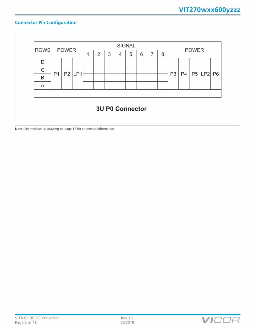
VIT270wxx600yzzz
3U P0 Connector
P1 P2 LP1
1 2 3 4 5 6 7 8
P3 P4 P5 LP2 P6
ROWSSIGNAL
POWER POWER
DCBA
Connector Pin Configuration
Note: See mechanical drawing on page 17 for connector information.

VITA 62 DC-DC Converter Rev 1.2Page 3 of 18 05/2019
VIT270wxx600yzzz
Connector Pin Descriptions
Pin Function / Name Description
P1 –DC_IN VIN–
P2 +DC_IN VIN+
LP1 CHASSIS Chassis
A1 No Connection
B1 No Connection
C1 No Connection
D1 No Connection
A2 No Connection
B2 FAIL*When any of the output is not within specification, FAIL* signal will be driven low to indicate a failure
C2 INHIBIT* Input control signal as defined in VITA 62, referenced to SIGNAL_RETURN
D2 ENABLE* Input control signal as defined in VITA 62, referenced to SIGNAL_RETURN
A3 No Connection
B3 +12VAUX +12V auxiliary output voltage
C3 No Connection
D3 No Connection
A4, B4, C4, D4 +3.3VAUX +3.3V auxiliary output voltage
A5 *GA0 Geographical address defined by VITA 46.11
B5 *GA1 Geographical address defined by VITA 46.11
C5 SM0 (I2C Clock)Primary I2C™ communication bus
D5 SM1 (I2C Data)
A6 I2C ClockRedundant I2C communication bus (optional feature pending)
B6 I2C Data
C6 –12VAUX –12V auxiliary output voltage
D6 SYS_RESET* System Reset is actively low. It will float when all outputs are within specification
A7 No Connection
B7 No Connection
C7 No Connection
D7 SIGNAL_RETURN Ground pin for control signals
A8 +12VSENSE VS1 sense, should be connected at point-of-load or on the backplane to corresponding voltage output
B8 +3.3VSENSE VS2 sense, should be connected at point-of-load or on the backplane to corresponding voltage output
C8 +5VSENSE VS3 sense, should be connected at point-of-load or on the backplane to corresponding voltage output
D8 SENSE_RETURN Should be connected to POWER_RETURN either remotely or at the connector
P3 +5VMAIN VS3
P4, P5 POWER_RETURN Common output voltage return pin
LP2 +3.3VMAIN VS2
P6 +12VMAIN VS1

VITA 62 DC-DC Converter Rev 1.2Page 4 of 18 05/2019
VIT270wxx600yzzz
Part Ordering Information
ProductFunction
Nominal Input Voltage GradePackage
SizeOutput Power Conformal Coated
Output Voltage Configuration
VIT 270 w xx 600 y zzz
VIT = VITA62 270 = 270VDC H = –40 to 85ºC 3U 600 = 600WB = Bare
C = Coated001 = Standalone002 = Parallelable
Absolute Maximum Ratings
The absolute maximum ratings below are stress ratings only. Operation at or beyond these maximum ratings can cause permanent damage to the device.
Parameter Comments Min Max Unit
Total Output Power Combined outputs for all rails 600 W
Input Voltage +IN to –IN –0.5 460 V
Operating Temperature Measured at card edge –40 85ºC
Storage Temperature –40 125
Isolation Voltage IN to OUT 1000 VDC
Isolation Voltage IN to CASE 1000 VDC
Isolation Voltage OUT to CASE 100 V
VITA 62 DC-DC Converter Rev 1.2Page 5 of 18 05/2019
VIT270wxx600yzzz
Electrical Characteristics
All data at nominal line and nominal load unless otherwise specified.
Attribute Symbol Conditions / Notes Min Typ Max Unit
Overall System Characteristics
System Efficiency
Nominal line, 20% aggregate loads 83
%Nominal line, 50% aggregate loads 89
Nominal line, 100% aggregate loads 89
Power Input Characteristics
Operating Input Voltage Range Full load 220 270 320 V
Transient 450 V
Input Current (No Load)270V Input, enable asserted (input on), inhibit de-asserted (output on)
30 75 mA
Inrush Current Peak no load, high line 1.4 5 A
Main Outputs
+12V Output
Output Voltage Set Point Nominal line, nominal load 11.9 12 12.1 V
Line Regulation 50% load 0.12 0.2 %
Load Regulation Nominal line 0.5 %
Output Ripple / Noise (Peak-to-Peak) Nominal line over load range, 20MHz BW 50.4 120 mVP-P
Maximum Capacitive Load External 9000 µF
Output Current Range 0 40 A
Output Overvoltage Protection Two consecutive OVP events to trip 13.2 V
Output Overcurrent Protection Three consecutive OCP events to trip 48 A
+5V Output
Output Voltage Set Point Nominal line, nominal load 4.93 5.0 5.07 V
Line Regulation 50% load 0.15 %
Load Regulation Nominal line 0.5 1.1 %
Output Ripple / Noise (Peak-to-Peak) Nominal line over load range, 20MHz BW 20 50 mVP-P
Maximum Capacitive Load External 9000 µF
Output Current Range 0 30 A
Output Overvoltage Protection Two consecutive OVP events to trip 5.6 V
Output Overcurrent Protection Three consecutive OCP events to trip 40 A
VITA 62 DC-DC Converter Rev 1.2Page 6 of 18 05/2019
VIT270wxx600yzzz
Attribute Symbol Conditions / Notes Min Typ Max Unit
Main Outputs (Cont.)
+3.3V Output
Output Voltage Set Point Nominal line, nominal load 3.25 3.3 3.45 V
Line Regulation 50% load 0.15 %
Load Regulation Nominal line 0.6 1.2 %
Output Ripple / Noise (Peak-to-Peak) Nominal line over load range, 20MHz BW 20 50 mVP-P
Maximum Capacitive Load External 9000 µF
Output Current Range 0 20 A
Output Overvoltage Protection Two consecutive OVP events to trip 3.7 V
Output Overcurrent Protection 30 A
Auxilliary Outputs
–12V Output
Output Voltage Set Point Nominal line, nominal load –11.8 –12.00 –12.1 V
Line Regulation 50% load 0.15 %
Load Regulation Nominal line 1.66 2.0 %
Output Ripple / Noise (Peak-to-Peak) Nominal line over load range, 20MHz BW 15 120 mVP-P
Output Current Range 0 1 A
Output Overcurrent Protection 2 A
+12V Output
Output Voltage Set Point 11.9 12.00 12.1 V
Line Regulation 50% load 0.1 %
Load Regulation Nominal line 1.21 1.25 %
Output Ripple / Noise (Peak-to-Peak) Nominal line over load range, 20MHz BW 30 120 mVP-P
Output Current Range 0 1 A
Output Overcurrent Protection 2 A
+3.3V Output
Output Voltage Set Point 3.2 3.3 3.4 V
Line Regulation 50% load 0.14 %
Load Regulation Nominal line 2.0 2.5 %
Output Ripple / Noise (Peak-to-Peak) Nominal line over load range, 20MHz BW 50 mVP-P
Output Current Range 0 6 A
Output Overcurrent Protection 10 A
Electrical Characteristics (Cont.)
All data at nominal line and nominal load unless otherwise specified.

VITA 62 DC-DC Converter Rev 1.2Page 7 of 18 05/2019
VIT270wxx600yzzz
Application Characteristics
Figure 1 — Turn-on and turn-off characteristics at nominal line and nominal load, to main outputs
Figure 2 — Turn-on and turn-off time from enable to outputs
VITA 62 DC-DC Converter Rev 1.2Page 8 of 18 05/2019
VIT270wxx600yzzz
Application Characteristics (Cont.)
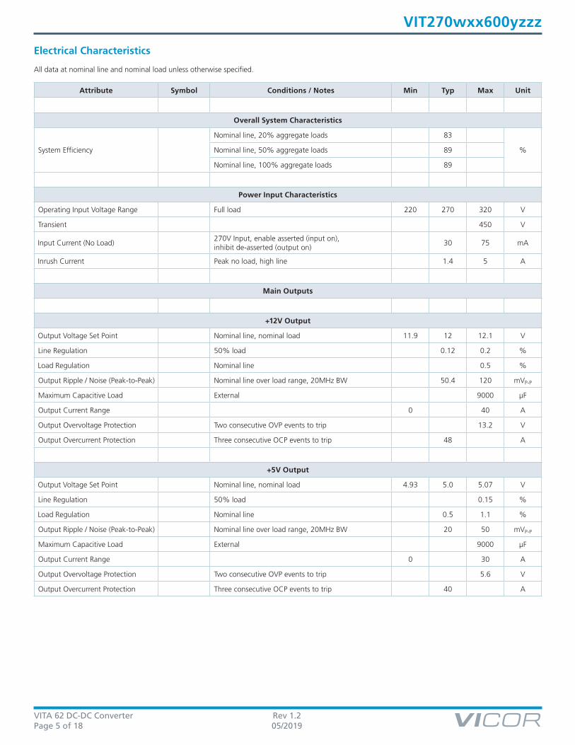
Figure 3 — Transient response, +12V output at nominal line, 10% – 90% – 10% load
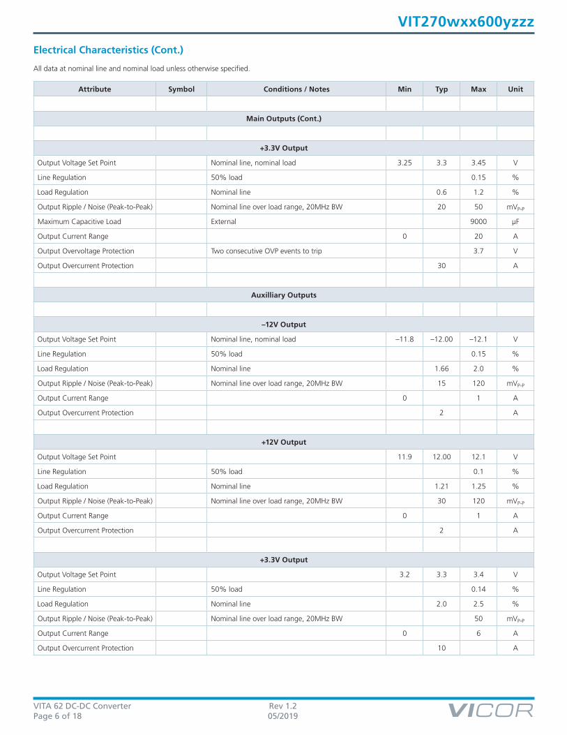
Figure 4 — Rise and fall, +12V output, nominal line, nominal load, enable/disable
VITA 62 DC-DC Converter Rev 1.2Page 9 of 18 05/2019
VIT270wxx600yzzz
Application Characteristics (Cont.)
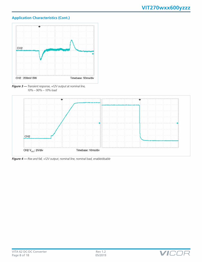
Figure 5 — Transient response, +5V output at nominal line, 10% – 90% – 10% load
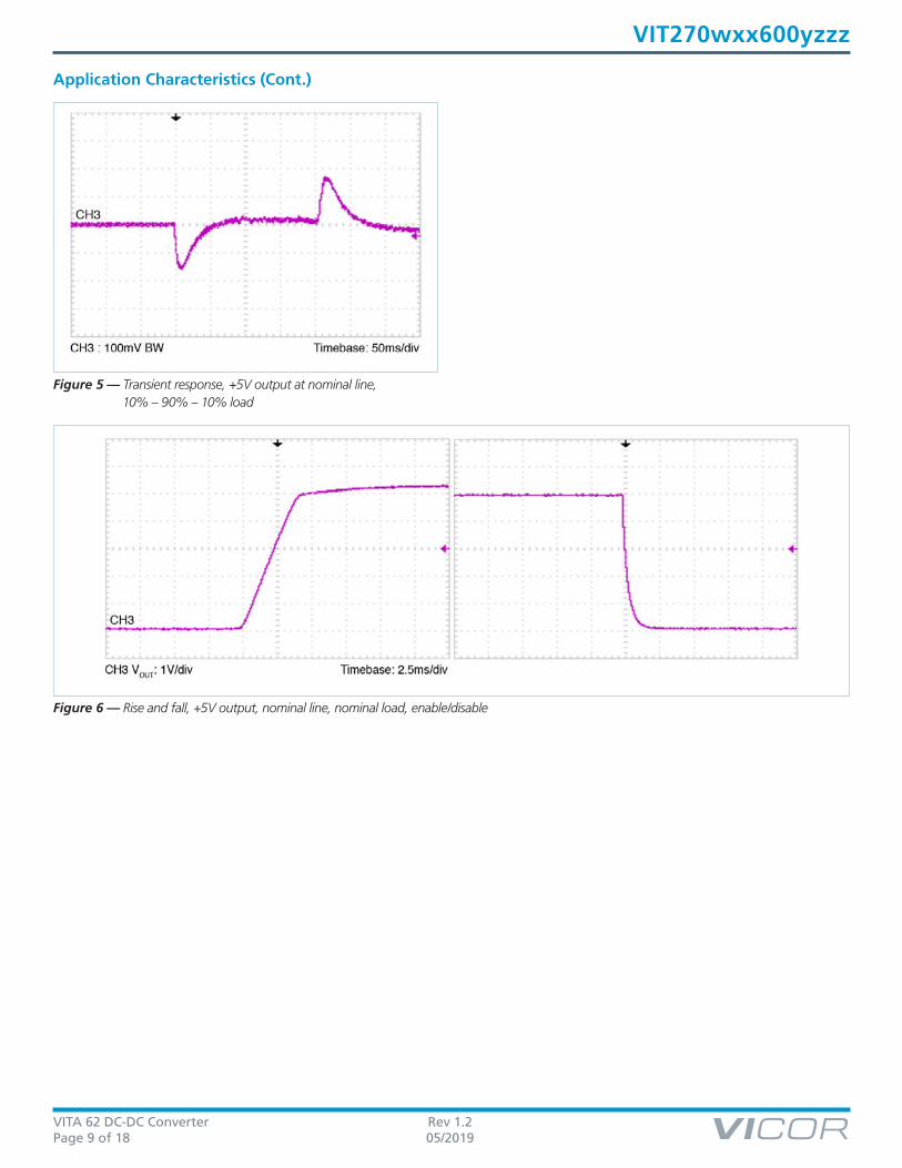
Figure 6 — Rise and fall, +5V output, nominal line, nominal load, enable/disable

VITA 62 DC-DC Converter Rev 1.2Page 10 of 18 05/2019
VIT270wxx600yzzz
Application Characteristics (Cont.)
Figure 7 — Transient response, +3.3V output at nominal line, 10% – 90% – 10% load
Figure 8 — Rise and fall, +3.3V output, nominal line, nominal load, enable/disable

VITA 62 DC-DC Converter Rev 1.2Page 11 of 18 05/2019
VIT270wxx600yzzz
Conducted Emissions Testing
Professional Testing, EMI, IncMIL-STD-461, CE102, Conducted Emissions, Power LeadsLine 1 Measured Emissions
Frequency10K 100K 1M 10M
10
20
30
40
50
60
70
80
90
100
110
Am
plit
ud
e (d
BµV
)
Client: Freedom Power Systems
Project Number: 20125-10
EUT Name: 01-739-0003 Power Supply
Current Time -12:19:02 PM, Monday, July 09, 2018
Operator: Michael Anthony
Line Under Test: Power 270VDC input EUT Mode: FULL Load Note:
Limit Level
Ambient Scan
Measured Value
Professional Testing, EMI, IncMIL-STD-461, CE102, Conducted Emissions, Power LeadsLine 2 Measured Emissions
Frequency10K 100K 1M 10M
10
20
30
40
50
60
70
80
90
100
110
Am
plit
ud
e (d
BµV
)
Client: Freedom Power Systems
Project Number: 20125-10
EUT Name: 01-739-0003 Power Supply
Current Time -12:16:57 PM, Monday, July 09, 2018
Operator: Michael Anthony
Line Under Test: Return EUT Mode: FULL Load Note:
Limit Level
Ambient Scan
Measured Value
Figure 9 — Conducted emissions of 270VDC input at full load
Figure 10 — Conducted emissions of power return at full load
VITA 62 DC-DC Converter Rev 1.2Page 12 of 18 05/2019
VIT270wxx600yzzz
Conducted Emissions Testing (Cont.)
Professional Testing, EMI, IncMIL-STD-461, CE102, Conducted Emissions, Power LeadsLine 1 Measured Emissions
Frequency10K 100K 1M 10M
10
20
30
40
50
60
70
80
90
100
110
Am
plit
ud
e (d
BµV
)
Client: Freedom Power Systems
Project Number: 20125-10
EUT Name: 01-739-0003 Power Supply
Current Time -12:26:02 PM, Monday, July 09, 2018
Operator: Michael Anthony
Line Under Test: Power 270VDC input EUT Mode: NO Load Note:
Limit Level
Ambient Scan
Measured Value
Professional Testing, EMI, IncMIL-STD-461, CE102, Conducted Emissions, Power LeadsLine 2 Measured Emissions
Frequency10K 100K 1M 10M
10
20
30
40
50
60
70
80
90
100
110
Am
plit
ud
e (d
BµV
)
Client: Freedom Power Systems
Project Number: 20125-10
EUT Name: 01-739-0003 Power Supply
Current Time -12:28:31 PM, Monday, July 09, 2018
Operator: Michael Anthony
Line Under Test: Return EUT Mode: NO Load Note:
Limit Level
Ambient Scan
Measured Value
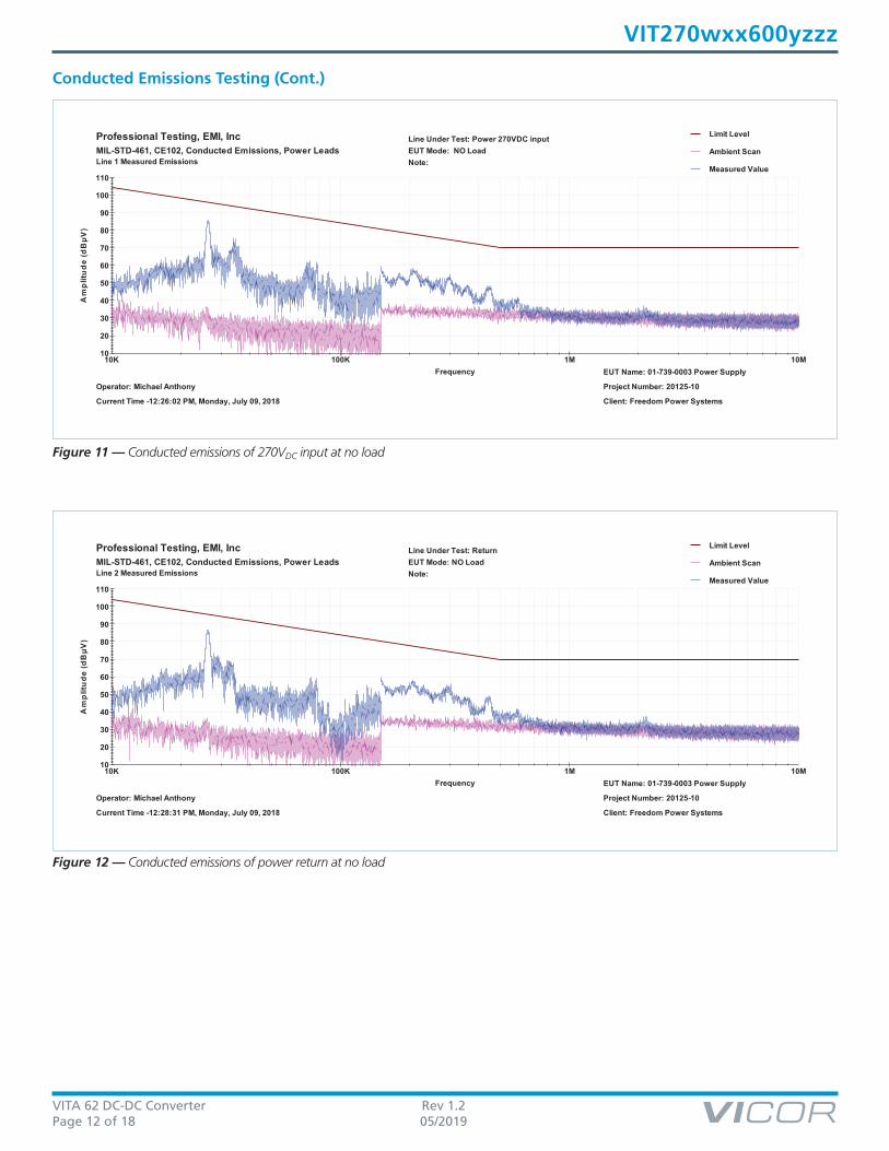
Figure 11 — Conducted emissions of 270VDC input at no load
Figure 12 — Conducted emissions of power return at no load
VITA 62 DC-DC Converter Rev 1.2Page 13 of 18 05/2019
VIT270wxx600yzzz
Attribute Symbol Conditions / Notes Min Typ Max Unit
Mechanical
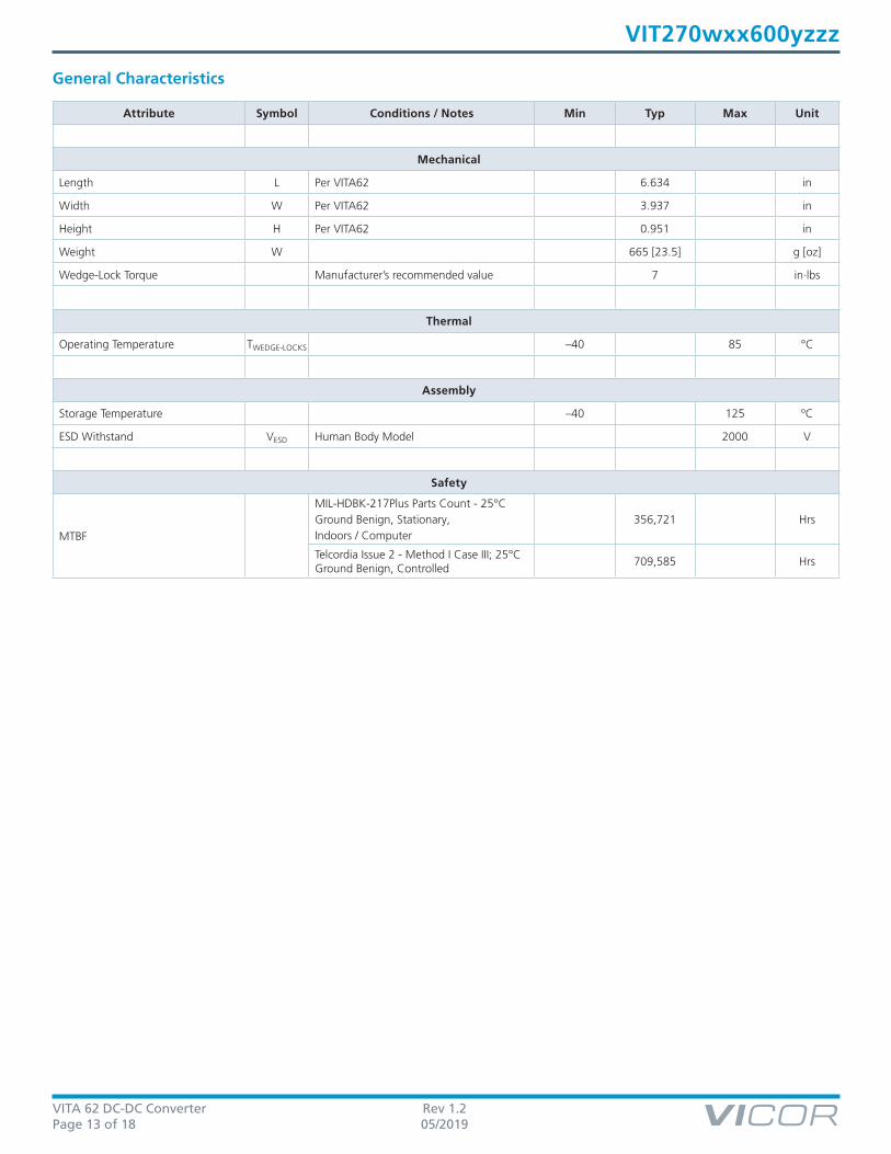
Length L Per VITA62 6.634 in
Width W Per VITA62 3.937 in
Height H Per VITA62 0.951 in
Weight W 665 [23.5] g [oz]
Wedge-Lock Torque Manufacturer’s recommended value 7 in.lbs
Thermal
Operating Temperature TWEDGE-LOCKS –40 85 °C
Assembly
Storage Temperature –40 125 ºC
ESD Withstand VESD Human Body Model 2000 V
Safety
MTBF
MIL-HDBK-217Plus Parts Count - 25°C Ground Benign, Stationary, Indoors / Computer
356,721 Hrs
Telcordia Issue 2 - Method I Case III; 25°C Ground Benign, Controlled
709,585 Hrs
General Characteristics

VITA 62 DC-DC Converter Rev 1.2Page 14 of 18 05/2019
VIT270wxx600yzzz
MIL-STD-461F
CE102 Power Lead10kHz – 10MHz FIGURE CE102‐1, 270V CurveSee Figures 9 – 12
Pass
CS101 Power Lead 30Hz – 150kHz Curve 1 Pass
CS114, Bulk Cable (Power) 10kHz – 200MHz Curve 5 Pass
CS114, Bulk Cables (I/O) 10kHz – 200MHz Curve 5 Pass
CS115 Bulk Cable (Power) Impulse Excitation FIGURE CS115‐1 Pass
CS115 Bulk Cables (I/O) Impulse Excitation FIGURE CS115‐1 Pass
CS116 Bulk Cable (Power)Damped Sinusoidal Transients 10kHz – 100MHz FIGURE CS116‐2
Pass
CS116 Bulk Cables (I/O)Damped Sinusoidal Transients 10kHz – 100MHz FIGURE CS116‐2
Pass
MIL‐STD‐704F‐7
Normal Transients HDC‐105 Pass
Abnormal Transients HDC‐302 Pass
Distortion Spectrum HDC‐103 Pass
MIL‐STD‐810G
Vibration Method 514.6 Procedure I
5 – 100Hz PSD increasing at 3dB/octave
Pass100 – 1000Hz PSD = 0.1g2/Hz
1000 – 2000Hz PSD decreasing at 6dB/octave
Operating Shock, Method 516 Procedure I40g, 11ms shock half‐sine
Pass40g, 11ms, terminal saw tooth shock pulses in all three axes
Standards Compliance
VITA 62 DC-DC Converter Rev 1.2Page 15 of 18 05/2019
VIT270wxx600yzzz
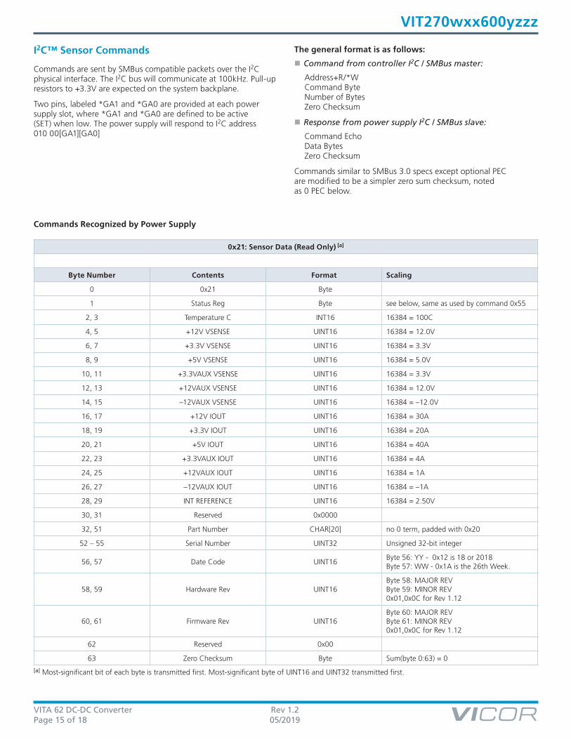
I2C™ Sensor Commands
Commands are sent by SMBus compatible packets over the I2C physical interface. The I2C bus will communicate at 100kHz. Pull-up resistors to +3.3V are expected on the system backplane.
Two pins, labeled *GA1 and *GA0 are provided at each power supply slot, where *GA1 and *GA0 are defined to be active (SET) when low. The power supply will respond to I2C address 010 00[GA1][GA0]
The general format is as follows:
�� Command from controller I2C / SMBus master:
Address+R/*W Command Byte Number of Bytes Zero Checksum
�� Response from power supply I2C / SMBus slave:
Command Echo Data Bytes Zero Checksum
Commands similar to SMBus 3.0 specs except optional PEC are modified to be a simpler zero sum checksum, noted as 0 PEC below.
Commands Recognized by Power Supply
[a] Most-significant bit of each byte is transmitted first. Most-significant byte of UINT16 and UINT32 transmitted first.
0x21: Sensor Data (Read Only) [a]
Byte Number Contents Format Scaling
0 0x21 Byte
1 Status Reg Byte see below, same as used by command 0x55
2, 3 Temperature C INT16 16384 = 100C
4, 5 +12V VSENSE UINT16 16384 = 12.0V
6, 7 +3.3V VSENSE UINT16 16384 = 3.3V
8, 9 +5V VSENSE UINT16 16384 = 5.0V
10, 11 +3.3VAUX VSENSE UINT16 16384 = 3.3V
12, 13 +12VAUX VSENSE UINT16 16384 = 12.0V
14, 15 –12VAUX VSENSE UINT16 16384 = –12.0V
16, 17 +12V IOUT UINT16 16384 = 30A
18, 19 +3.3V IOUT UINT16 16384 = 20A
20, 21 +5V IOUT UINT16 16384 = 40A
22, 23 +3.3VAUX IOUT UINT16 16384 = 4A
24, 25 +12VAUX IOUT UINT16 16384 = 1A
26, 27 –12VAUX IOUT UINT16 16384 = –1A
28, 29 INT REFERENCE UINT16 16384 = 2.50V
30, 31 Reserved 0x0000
32, 51 Part Number CHAR[20] no 0 term, padded with 0x20
52 – 55 Serial Number UINT32 Unsigned 32-bit integer
56, 57 Date Code UINT16Byte 56: YY - 0x12 is 18 or 2018Byte 57: WW - 0x1A is the 26th Week.
58, 59 Hardware Rev UINT16Byte 58: MAJOR REVByte 59: MINOR REV0x01,0x0C for Rev 1.12
60, 61 Firmware Rev UINT16Byte 60: MAJOR REVByte 61: MINOR REV0x01,0x0C for Rev 1.12
62 Reserved 0x00
63 Zero Checksum Byte Sum(byte 0:63) = 0

VITA 62 DC-DC Converter Rev 1.2Page 16 of 18 05/2019
VIT270wxx600yzzz
Commands Recognized by Power Supply (Cont.)
Status Register Bit Map (Byte 1) used in command 0x55
Bit 0 and 1 allow you to monitor what the power supply is reading from the input connector.
0x44: Firmware Date (Read Only) [a]
• Uses SMBus Read 64 type protocol similar to section 6.5.13, but extended to 16 bytes, with or without 0 PEC
Byte Number Contents Format Typical Value
0 0x44 Byte
1 – 4 Year CHAR[4] 2018
5, 6 Month CHAR[2] 12
7, 8 Day CHAR[2] 31
9, 10 Hour CHAR[2] 23
11, 12 Minute CHAR[2] 59
13, 14 Second CHAR[2] 42
15 Zero Checksum Byte Sum(byte 0:15) = 0
0x45: Hardware Address (Read Only) [a]
• Uses SMBus Read Byte protocol, section 6.5.5, with or without 0 PEC
Byte Number Contents Format Typical Value
0 0x45 Byte
1 I2C Address Byte 0x23, set by *GA1, *GA0
2 Zero Checksum Byte Sum(byte 0:2) = 0
0x55: Status Command (Read/Write) [a]
• Uses SMBus Wirte Byte/Read Byte protocol, section 6.5.4, 6.5.5, with or without 0 PEC
Byte Number Contents Format Typical Value
0 0x55 Byte
1 Status Byte Byte 0x18 = All outputs ON
2 Zero Checksum Byte Sum(byte 0:2) = 0
*HW En*HW Inh
*SW En
*SW Inh
XFAIL
OT Warning
SW Priority
Read/Write
7 6 5 4 3 2 1 0
0 0 0 0 0 00 0
STATUS REGISTER (Byte 1)(0x55)
Bit Name Condition Default
7 X 0 0
6 FAILIf set to 1 my System Manager,
a fault condition will clear this bit.0
5 OT WarningIf set to 1 my System Manager, an OT fault will clear this bit.
0
4 SW Priority Set to 1 for SW Control 0
3 *SW lnh EN all, 0 EN only 3.3V 0
2 *SW En ALL outputs regardless 0
1 *HW lnh As read by HW BACKPLANE
0 *HW En As read by HW BACKPLANE
[a] Most-significant bit of each byte is transmitted first. Most-significant byte of UINT16 and UINT32 transmitted first.

VITA 62 DC-DC Converter Rev 1.2Page 17 of 18 05/2019
VIT270wxx600yzzz
Mechanical Drawing
3.937
3.197
6.634
3.335 .301
THERMAL SEATING PLANE
.951
.257
.393
.495 NOMINAL,WEDGE-LOCKEXPANDS TO.545 MAX.
1 2 3
DIMENSION ARE IN INCHES
Connector Components
Item # Description Manufacturer Manufacturer Part Number
1 VITA46 0 DEG Guide Socket TE Connectivity 1-1469492-1
2 VITA62 Connector Plug TE Connectivity 6450849-7
3 VITA46 315 DEG Guide Socket TE Connectivity 1-1469492-8

VITA 62 DC-DC Converter Rev 1.2Page 18 of 18 05/2019
VIT270wxx600yzzz
Revision History
Revision Date Description Page Number(s)
1.0 08/21/18 Initial release n/a
1.1 10/15/18
Updated features & benefits, product descriptionUpdated connector pin descriptionsUpdated current specs for main +3.3V outputUpdated 0x21 tableUpdated command 0x55 table
1361516
1.2 05/30/19Updated output ripple/noise specs for –12V and +12V outputsUpdated MIL-STD-461F CS114 standards compliance to “pass”
614
Contact Us: http://www.vicorpower.com/contact-us
Vicor Corporation25 Frontage Road
Andover, MA, USA 01810Tel: 800-735-6200Fax: 978-475-6715
www.vicorpower.com
emailCustomer Service: [email protected]
Technical Support: [email protected]
©2018 – 2019 Vicor Corporation. All rights reserved. The Vicor name is a registered trademark of Vicor Corporation.I2C™ is a trademark of NXP semiconductor.
All other trademarks, product names, logos and brands are property of their respective owners.