
Vissim Digital Power User Guide
269
Version 8.0 VisSim Digital Power Designer Suite User’s Guide By Visual Solutions Inc.
Transcript of Vissim Digital Power User Guide

Version 8.0
VisSim Digital Power Designer Suite User’s Guide
By Visual Solutions Inc.

Version 8.0 VisSim Digital Power Designer Suite User’s Guide
0.2
Visual Solutions, Inc.
VisSim Digital Power Designer User's Guide for VisSim Version 8.0
Copyright © 2012 Visual Solutions, Inc. Visual Solutions, Inc.
All rights reserved. 487 Groton Road
Westford, MA 01886
Trademarks VisSim, VisSim/Analyze, VisSim/CAN, VisSim/C-Code, VisSim/CCode
Support Library source, VisSim/Comm, VisSim/Comm C-Code,
VisSim/Comm Red Rapids, VisSim/Comm Turbo Codes,
VisSim/Comm Wireless LAN, VisSim/Fixed-Point, VisSim/Knobs &
Gauges, VisSim/Model-Wizard, VisSim/Motion, VisSim/Neural-Net,
VisSim/OPC, VisSim/OptimzePRO, VisSim/Real-TimePRO,
VisSim/State Charts, VisSim/Serial, VisSim/UDP, VisSim
Viewer,and flexWires are trademarks of Visual Solutions. All other
products mentioned in this manual are trademarks or registered
trademarks of their respective manufacturers.
Copyright and use
restrictions
The information in this manual is subject to change without notice and
does not represent a commitment by Visual Solutions. Visual
Solutions does not assume any responsibility for errors that may
appear in this document.
No part of this manual may be reprinted or reproduced or utilized in
any form or by any electronic, mechanical, or other means without
permission in writing from Visual Solutions. The Software may not be
copied or reproduced in any form, except as stated in the terms of the
Software License Agreement.
DPBS Block set release version 1.0.0
Version 8.0 VisSim Digital Power Designer Suite User’s Guide
0.3
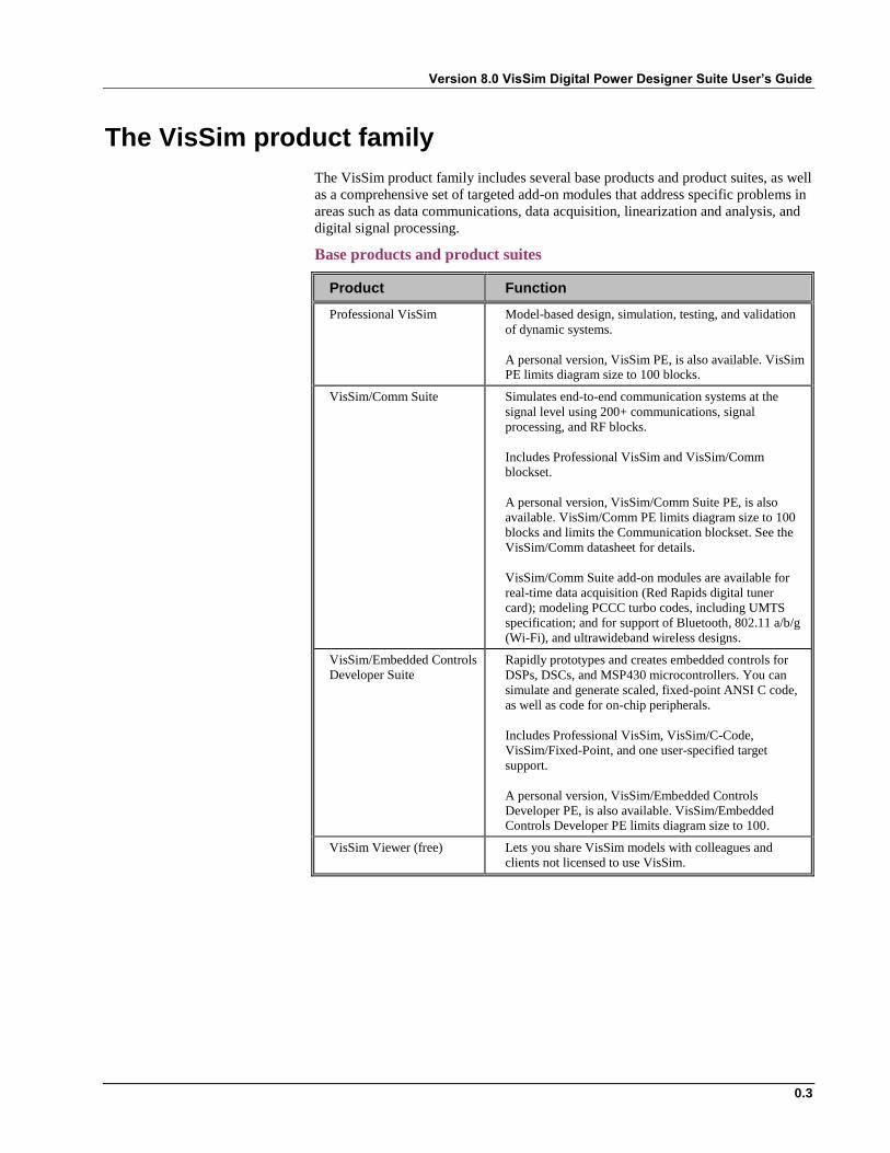
The VisSim product family
The VisSim product family includes several base products and product suites, as well
as a comprehensive set of targeted add-on modules that address specific problems in
areas such as data communications, data acquisition, linearization and analysis, and
digital signal processing.
Base products and product suites
Product Function
Professional VisSim Model-based design, simulation, testing, and validation
of dynamic systems.
A personal version, VisSim PE, is also available. VisSim PE limits diagram size to 100 blocks.
VisSim/Comm Suite Simulates end-to-end communication systems at the
signal level using 200+ communications, signal
processing, and RF blocks.
Includes Professional VisSim and VisSim/Comm
blockset.
A personal version, VisSim/Comm Suite PE, is also
available. VisSim/Comm PE limits diagram size to 100
blocks and limits the Communication blockset. See the
VisSim/Comm datasheet for details.
VisSim/Comm Suite add-on modules are available for
real-time data acquisition (Red Rapids digital tuner
card); modeling PCCC turbo codes, including UMTS
specification; and for support of Bluetooth, 802.11 a/b/g
(Wi-Fi), and ultrawideband wireless designs.
VisSim/Embedded Controls
Developer Suite
Rapidly prototypes and creates embedded controls for
DSPs, DSCs, and MSP430 microcontrollers. You can
simulate and generate scaled, fixed-point ANSI C code,
as well as code for on-chip peripherals.
Includes Professional VisSim, VisSim/C-Code,
VisSim/Fixed-Point, and one user-specified target
support.
A personal version, VisSim/Embedded Controls
Developer PE, is also available. VisSim/Embedded Controls Developer PE limits diagram size to 100.
VisSim Viewer (free) Lets you share VisSim models with colleagues and
clients not licensed to use VisSim.

Version 8.0 VisSim Digital Power Designer Suite User’s Guide
0.4
Add-on modules
Add-On Module Function
VisSim/Analyze Performs frequency domain analysis of a linearized
nonlinear subsystem.
VisSim/CAN Interfaces with a USB CAN device to read and write
CAN messages on the CAN bus.
VisSim/C-Code Generates highly-optimized, ANSI C code that can be
compiled and run on any platform that supports an ANSI C compiler.
VisSim/C-Code Support
Library Source
Provides source code for the Support Library.
VisSim/Comm blockset Simulates end-to-end communication systems at the
signal level using 200+ communications, signal processing, and RF blocks.
A personal version, VisSim/Comm PE, is also available.
VisSim/Comm PE is a subset of the Communication
blockset. See the VisSim/Comm datasheet for details
You can purchase VisSim/Comm add-on modules for
real-time data acquisition (Red Rapids digital tuner
cards); for modeling PCCC turbo codes, including
UMTS specification; for support of Bluetooth, 802.11 a/b/g (Wi-Fi), and ultrawideband wireless designs.
VisSim/Digital Power
Designer Suite
Provides high-level blocks for digital power applications
and power supply design.
VisSim/Fixed-Point Simulates the behavior of fixed-point algorithms prior to
code generation and implementation of the algorithm on the fixed-point target.
VisSim/Knobs and Gauges Provides dynamic gauges, meters, and knobs for process
control, and measurement and validation systems.
VisSim/Model-Wizard Generates transfer function model from historic or real-
time data.
VisSim/Motion Simulates motor control systems with customizable
amplifiers, controllers, filters, motors, sensors, sources, tools, and transforms.
VisSim/Neural-Networks Performs nonlinear system identification, problem
diagnosis, decision-making prediction, and other
problems where pattern recognition is important.
VisSim/OPC Connects to any OPC server and log data or run a virtual
plant in VisSim for offline tuning.
VisSim/OptimizePRO Performs generalized reduced gradient method of
parameter optimization.
VisSim/Real-TimePRO Performs real-time data acquisition and signal generation
using I/O cards, PLCs, and DCSs.
VisSim/Serial Performs serial I/O with other computers.
VisSim/State Charts Creates, edits, and executes event-based systems.
VisSim/UDP Performs data exchange over the internet using UDP.
VisSim Viewer (free) Lets you share VisSim models with colleagues and
clients not licensed to use VisSim.

Version 8.0 VisSim Digital Power Designer Suite User’s Guide
0.5
Resources for learning VisSim/Digital Power
For those of you that are new to VisSim, we have provided several free services to
make your transition to VisSim fast, smooth, and easy:
Interactive webinars
VisSim movies
Sample diagrams
Interactive webinars
Interactive webinars offer you the opportunity to meet with Visual Solutions product
specialists who will introduce and demonstrate our software products live on your
computer and answer any questions you have. Each webinar is approximately 45
minutes long. To learn more about our interactive webinars, go to
http://www.vissim.com/webinars/webinars.html.
VisSim movies
Designed by Visual Solutions application engineers, the VisSim movies guide you
through the creation, simulation, debugging, and optimizing of block diagrams that
cover a broad range of engineering disciplines.
You can access the movies from your VisSim CD under the \MOVIES directory. Or,
you can go to http://www.vissim.com/support/vissim_instructional_movies.html and
download the movies to your computer.
Sample diagrams
VisSim 8.0 includes a directory of fully documented sample diagrams. These
diagrams illustrate both simple and complex models spanning a broad range of
engineering disciplines, including aerospace, biophysics, chemical engineering,
control design, dynamic systems, electromechanical systems, environmental systems,
HVAC, motion control, process control, and signal processing.
To access sample diagrams
Click on the Diagrams menu in VisSim.
Click on Examples Applications.
To access Digital Power example diagrams
Click on the Digital Power Examples menu in VisSim.
Training Visual Solutions offers training sessions for learning and gaining expertise in VisSim
and the VisSim family of add-on products. Training sessions are conducted at Visual
Solutions training facility in Westford, MA, as well as at customer sites and as online
webinars.
For information on setting up a training session, contacts [email protected].
Version 8.0 VisSim Digital Power Designer Suite User’s Guide
0.6
Digital Power Designer Suite
The VisSim Digital Power Designer Suite consists of the following
add-ons:
Digital Power Block Set (DPBS).
Version 8.0 VisSim Digital Power Designer Suite User’s Guide
0.7
Contents
Introduction ……………………………………………………………. Chapter 1
Block Reference – Components …………………………………. Chapter 2
Block Reference – Simulation ……………………………………. Chapter 3
Block Reference – Tools …………………………………………….. Chapter 4

Chapter 1 - Contents
INTRODUCTION............................................................................................................................................. 2
Disclaimer ..................................................................................................................................................................... 3
Requirements for the Digital Power Designer Suite ...................................................................................................... 4
Installing the Digital Power Designer Suite ................................................................................................................... 4
Overview of Digital Power Applications ........................................................................................................................ 6
Overview of the Digital Power Designer Suite .............................................................................................................. 7
Digital Power Designer Suite in Sections ....................................................................................................................... 8

Version 8.0 VisSim Digital Power Designer Suite User’s Guide
Introduction 1.2
Introduction
The VisSim digital power designer suite is a series of add-ons to the VisSim 8
standard block set with application specific blocks for analog and digital power
applications. The various sections of the suite can be used independently or together
to form a powerful design suite package for digital power supply design and other
digital power applications.
One can quickly navigate throughout this user’s guide by clicking on any contents
item to jump to that block description or section. In many parts of the user’s guide,
the word:
Back
can be found which will return the reader back to the chapter contents for further
navigation.

Version 8.0 VisSim Digital Power Designer Suite User’s Guide
1.3 Introduction
Disclaimer
The simulations, component values and eventually the code generated, as well as the
overall functionality of the diagrams developed within the digital power designer
suite are indicative only to assist the power supply design engineer in the many
phases of analog and digital power supply design.
The responsibility of selecting the correct parameters and component values is
explicitly left with the power supply design engineer. The purpose of the digital
power designer suite is to provide the digital power designer with a tool to assist in
the design of power supplies and other digital power applications.
Visual Solutions, its representatives and its subcontractors take no responsibility for
the selection of incorrect parameters and / or components due to calculations or
simulations generated within the digital power block set, or for any damage or
personal harm which may occur due to the selection of incorrect parameters and / or
components.
At the time of testing this tool, all calculations, based upon the given assumptions
and limitations, were believed to be correct. However, it is the responsibility of the
power supply design engineer to verify any calculations and simulations used in a
design or as a teaching tool. Visual Solutions, its representatives and its
subcontractors take no responsibility for any damage, in any form, which may occur
due to incorrect calculations or incorrect reported outputs of the design suite, nor for
any incorrect use of this software.
The digital power design suite will be upgraded regularly for improvements to
performance, to add features or to correct any calculation which may be found to be
inaccurate. It is the responsibility of the end user to check regularly on the Visual
Solutions website for updates of the Digital Power Designer Suite.
Updates can be found here:
http://www.vissim.com/downloads/vissim_software.html
All detailed assumptions and/or limitations of this tool must be taken into account
before applying any of the calculated values to a given design. These assumptions
and limitations are outlined in the various readme blocks throughout the designer
suite installed software under the digital power menu within VisSim. Although care
has been taken to outline as many of the assumptions and limitations as possible, the
assumptions listed are not guaranteed to be a complete list of assumptions and
limitations. Correct performance must be verified on the designated hardware.
As is always good practise, all designs must be thoroughly tested on the destined
hardware and verified for correct performance, in all expected life-cycle conditions,
by the power supply design engineer.
Version 8.0 VisSim Digital Power Designer Suite User’s Guide
Introduction 1.4
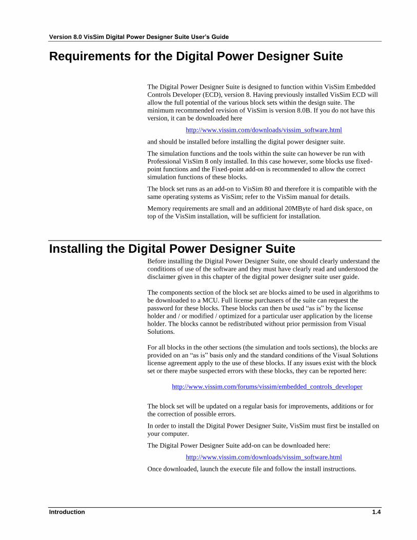
Requirements for the Digital Power Designer Suite
The Digital Power Designer Suite is designed to function within VisSim Embedded
Controls Developer (ECD), version 8. Having previously installed VisSim ECD will
allow the full potential of the various block sets within the design suite. The
minimum recommended revision of VisSim is version 8.0B. If you do not have this
version, it can be downloaded here
http://www.vissim.com/downloads/vissim_software.html
and should be installed before installing the digital power designer suite.
The simulation functions and the tools within the suite can however be run with
Professional VisSim 8 only installed. In this case however, some blocks use fixed-
point functions and the Fixed-point add-on is recommended to allow the correct
simulation functions of these blocks.
The block set runs as an add-on to VisSim 80 and therefore it is compatible with the
same operating systems as VisSim; refer to the VisSim manual for details.
Memory requirements are small and an additional 20MByte of hard disk space, on
top of the VisSim installation, will be sufficient for installation.
Installing the Digital Power Designer Suite Before installing the Digital Power Designer Suite, one should clearly understand the
conditions of use of the software and they must have clearly read and understood the
disclaimer given in this chapter of the digital power designer suite user guide.
The components section of the block set are blocks aimed to be used in algorithms to
be downloaded to a MCU. Full license purchasers of the suite can request the
password for these blocks. These blocks can then be used “as is” by the license
holder and / or modified / optimized for a particular user application by the license
holder. The blocks cannot be redistributed without prior permission from Visual
Solutions.
For all blocks in the other sections (the simulation and tools sections), the blocks are
provided on an “as is” basis only and the standard conditions of the Visual Solutions
license agreement apply to the use of these blocks. If any issues exist with the block
set or there maybe suspected errors with these blocks, they can be reported here:
http://www.vissim.com/forums/vissim/embedded_controls_developer
The block set will be updated on a regular basis for improvements, additions or for
the correction of possible errors.
In order to install the Digital Power Designer Suite, VisSim must first be installed on
your computer.
The Digital Power Designer Suite add-on can be downloaded here:
http://www.vissim.com/downloads/vissim_software.html
Once downloaded, launch the execute file and follow the install instructions.

Version 8.0 VisSim Digital Power Designer Suite User’s Guide
1.5 Introduction
It is highly recommended to install to the default directory within the VisSim80
folder (i.e. C:\VisSim80\Digital Power). Otherwise, some of the links maybe invalid.
If it is necessary to install to a different folder then the Include directory should be
placed in the location C:\VisSim80\Digital Power\Include. It is also recommended to
place the folder ExportFiles in C:\VisSim80\Digital Power\ExportFiles.
A “Digital Power” menu will be installed within the VisSim IDE consisting of high-
level digital power application-specific blocks and many examples to quickly come
up to speed with the design suite and with digital power design techniques.

Version 8.0 VisSim Digital Power Designer Suite User’s Guide
Introduction 1.6
Overview of Digital Power Applications
Digital power is ever more present in power supply design due to its many
advantages and the readily available and powerful microcontrollers which these days
have many integrated peripherals dedicated to digital power applications at an ever
reducing cost.
Microcontrollers or MCUs, integrate complex PWMs, analog-to-digital converters
(ADCs), digital-to-analog converters (DACs), fast comparators and other peripheral
hardware integration dedicated to digital power applications. Much of the traditional
hardware which was required to support MCUs such as supply voltage monitors,
voltage regulators and oscillators have also been integrated within the MCU,
decreasing further the cost, printed circuit board footprint and the hardware
complexity of a given design.
A very good overview of digital power can be found in the document slup232 - “A
Practical Introduction to Digital Power Supply Control” by Laszlo Balogh which can
found at:
http://www.ti.com/lit/ml/slup232/slup232.pdf
The main advantage of digital power is the flexibility of the design. As soon as a
hardware platform is developed, digital power can allow the implementation of that
hardware to many varying applications or application areas. This can speed up the
time to market for new products once a base hardware and software has been
developed. An MCU can provide the integrated components and processing power
necessary for the control loop and it can also provide communications capabilities
for interfacing the power supply to the outside world (HMI), power supply
monitoring and parallel current sharing communications can also be easily integrated
with very little additional hardware. Digital power supplies can be simply integrated
into a given system operating other equipment, via standard communication
protocols.
Control parameters can be varied during the normal operation of a power supply;
something that would be very difficult to implement in analog control. Digital
control parameters can be optimized according to the current environmental
conditions or due to the aging of analog / power components during the normal life-
cycle of a power supply. Once set, the parameters in digital control will remain
constant and will not vary due to temperature variations or aging of components.
Compared with analog control, a much larger range of effective component values is
available to the designer by simply choosing numerical values within the software.
Custom control algorithms can be flexibly applied using digital control.
For the analog designer, the main obstacle to digital power applications is the initial
complexity of the design and the difficulty of implementing control algorithms
which require new techniques which the traditional analog designer is either not
accustomed to or does not remember from their university days. The unfamiliarity
with digital power design techniques is an issue which needs to be addressed for the
continued growth of digital power.
The VisSim digital power designer suite is aimed particularly at assisting the power
supply designer with a purely analog background, to overcome this hurdle while at
the same time offering many tools and dedicated blocks to aid the designer, either
from a digital or analog background, in any type of power supply design.

Version 8.0 VisSim Digital Power Designer Suite User’s Guide
1.7 Introduction
Overview of the Digital Power Designer Suite
The VisSim Digital Power Designer Suite is aimed to provide the power supply
design engineer with a tool to design and develop power supplies and in particular
digital power supplies. It is the intention to regularly upgrade this tool with more
features and more add-ons to provide a complete power supply design solution.
There are several environments in the VisSim Digital Power Designer Suite;
simulation , code-generation and tools. The tools assist in the various design stages
of designing digital power supplies, generally determining components and
parameters by calculation. The simulation environment provides many ready-made
blocks in order to quickly perform simulations of digital power supply applications.
The code generation environment provides many blocks which can be connected
together to form diagrams which can be automatically and effortlessly code-
generated, linked and compiled for a MCU thanks to the built-in VisSim code
generation features (VisSim ECD or the C-code add-on is needed).
Application areas for the VisSim Digital Power Designer Suite include all types of
power supply from low power (several Watts) to many Mega Watts . Some
application areas are power supply design, battery chargers and rectifiers, renewable
energy, LED lighting, Uninterruptible power supplies (UPS), DC-DC converters etc.

Version 8.0 VisSim Digital Power Designer Suite User’s Guide
Introduction 1.8
Digital Power Designer Suite in Sections
The VisSim Digital Power Designer Suite consists of many sections and several
sections of blocks. The main block sections are:
Components
Simulation
Tools
The components section consists of blocks with the normal cyan colouring which
have been optimized for downloading to an MCU to be used in digital power
applications. These blocks can be used in simulations or for code-generating.
The simulation section consists of a large number of blocks aimed at simulating
digital power supplies. The blocks within this section consist of models of typical
hardware components found in power supply design, hardware peripherals typically
found internally in MCUs designed for digital power applications as well as many
typical power converter configurations applied to the many application areas of
power supply design.
The tools section consists of blocks designed to assist the power supply design
engineer in the various aspects of power supply design including assistance in the
conversion from analog to digital power supply control techniques.
The following chapters outline the many blocks and their features and function for
each of these three sections.
Chapter 2 - Contents
BLOCK REFERENCE - COMPONENTS ...................................................................................................... 3
Compensators ............................................................................................................................................................... 4 1P1Z Compensator ........................................................................................................................................................... 4 1P1Z Compensator (with pins) ......................................................................................................................................... 5 2P2Z Compensator ........................................................................................................................................................... 6 2P2Z Compensator (with pins) ......................................................................................................................................... 7 3P3Z Compensator ........................................................................................................................................................... 8 3P3Z Compensator (with pins) ......................................................................................................................................... 9 PI compensator ............................................................................................................................................................... 10 PID compensator (traditional) ........................................................................................................................................ 11
Controllers .................................................................................................................................................................. 12 Time slicer ....................................................................................................................................................................... 12 Voltage Mode Controller (VMC) ..................................................................................................................................... 13 Average Current Mode Controller (ACMC) ..................................................................................................................... 14 Hysteretic Current Mode Controller (HCMC) ................................................................................................................. 15 Zero-transition Current Mode Controller (ZCMC) .......................................................................................................... 16 Phase-shifting Full-bridge Voltage Mode Controller (PSFB-VMC) .................................................................................. 16
Filters .......................................................................................................................................................................... 18 First order filter (with pins) ............................................................................................................................................. 18 Second order filter .......................................................................................................................................................... 18 Second order filter (with pins) ........................................................................................................................................ 20 Moving average filter ...................................................................................................................................................... 20 Moving median filter ...................................................................................................................................................... 22
Measurements............................................................................................................................................................ 23 Average Value ................................................................................................................................................................. 23 RMS Value ....................................................................................................................................................................... 23 Minimum Value .............................................................................................................................................................. 24 Maximum Value .............................................................................................................................................................. 25 Real Power ...................................................................................................................................................................... 26 Reactive Power ............................................................................................................................................................... 27 Apparent Power .............................................................................................................................................................. 27 Power Factor ................................................................................................................................................................... 28 Crest Factor..................................................................................................................................................................... 28 Form Factor .................................................................................................................................................................... 29 THD ................................................................................................................................................................................. 29 Time - Frequency ............................................................................................................................................................ 30
Background ................................................................................................................................................................. 32 Soft Start (fixed-point) .................................................................................................................................................... 32 Soft start (FPU) ............................................................................................................................................................... 32 Event Counter ................................................................................................................................................................. 33

Version 8.0 VisSim Digital Power Designer Suite User’s Guide
Block Reference - Components 2.2
Window Comparator with Hysteresis ............................................................................................................................. 34 Window detector ............................................................................................................................................................ 35
Code-generable Control Loops .................................................................................................................................... 37 Voltage Mode Control (VMC) ......................................................................................................................................... 37 Peak Current Mode Control (PCMC) ............................................................................................................................... 39 Average Current Mode Control (ACMC) ......................................................................................................................... 39 Hysteretic Current Mode Control (HCMC) ...................................................................................................................... 40 Zero-transition Current Mode Control (ZCMC) .............................................................................................................. 40 Phase Shifting Full-bridge Voltage Mode Control (PSFB-VMC) ...................................................................................... 40
Frequently Used ......................................................................................................................................................... 41

Version 8.0 VisSim Digital Power Designer Suite User’s Guide
2.3 Block Reference - Components
Block Reference - Components
The components section of the digital power designer block set consists of a series of
blocks for digital power applications which can be code-generated and downloaded
to a MCU and in particular, the TI C2000 series of MCUs.
The blocks in this section are therefore optimized for operation on an MCU. The
blocks can also be used together with blocks from the simulation section to create
simulation diagrams.
Version 8.0 VisSim Digital Power Designer Suite User’s Guide
Block Reference - Components 2.4
Compensators
There are five different digital compensators (and three variants with input pins for
the coefficients) in the components section of the digital power block set. These
compensators are given in three forms:
1. 16-bit fixed point
2. 32-bit fixed point
3. FPU (floating point)
Here the 32-bit fixed point blocks are described and the other two forms have
identical characteristics except for the internal arithmetic format.
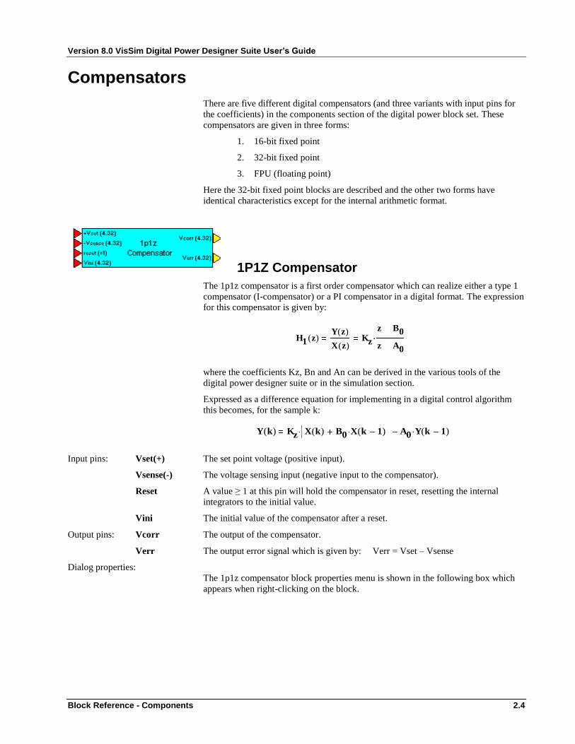
1P1Z Compensator
The 1p1z compensator is a first order compensator which can realize either a type 1
compensator (I-compensator) or a PI compensator in a digital format. The expression
for this compensator is given by:
where the coefficients Kz, Bn and An can be derived in the various tools of the
digital power designer suite or in the simulation section.
Expressed as a difference equation for implementing in a digital control algorithm
this becomes, for the sample k:
Input pins: Vset(+) The set point voltage (positive input).
Vsense(-) The voltage sensing input (negative input to the compensator).
Reset A value ≥ 1 at this pin will hold the compensator in reset, resetting the internal
integrators to the initial value.
Vini The initial value of the compensator after a reset.
Output pins: Vcorr The output of the compensator.
Verr The output error signal which is given by: Verr = Vset – Vsense
Dialog properties:
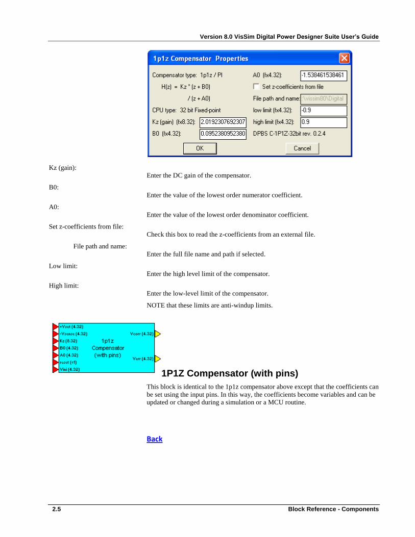
The 1p1z compensator block properties menu is shown in the following box which
appears when right-clicking on the block.
H1 z( )Y z( )
X z( )Kz
z B0
z A0
Y k( ) Kz X k( ) B0 X k 1( ) A0 Y k 1( )
Version 8.0 VisSim Digital Power Designer Suite User’s Guide
2.5 Block Reference - Components
Kz (gain):
Enter the DC gain of the compensator.
B0:
Enter the value of the lowest order numerator coefficient.
A0:
Enter the value of the lowest order denominator coefficient.
Set z-coefficients from file:
Check this box to read the z-coefficients from an external file.
File path and name:
Enter the full file name and path if selected.
Low limit:
Enter the high level limit of the compensator.
High limit:
Enter the low-level limit of the compensator.
NOTE that these limits are anti-windup limits.
1P1Z Compensator (with pins)
This block is identical to the 1p1z compensator above except that the coefficients can
be set using the input pins. In this way, the coefficients become variables and can be
updated or changed during a simulation or a MCU routine.
Back
Version 8.0 VisSim Digital Power Designer Suite User’s Guide
Block Reference - Components 2.6
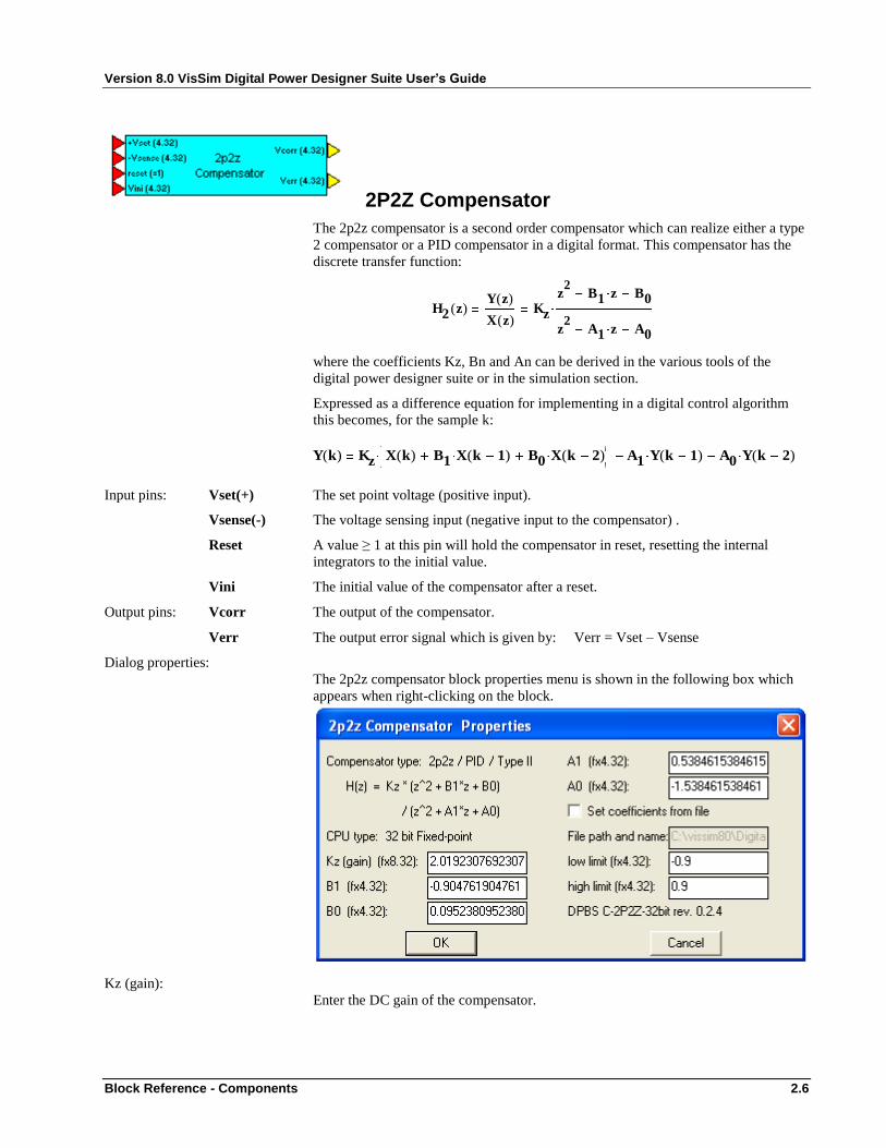
2P2Z Compensator
The 2p2z compensator is a second order compensator which can realize either a type
2 compensator or a PID compensator in a digital format. This compensator has the
discrete transfer function:
where the coefficients Kz, Bn and An can be derived in the various tools of the
digital power designer suite or in the simulation section.
Expressed as a difference equation for implementing in a digital control algorithm
this becomes, for the sample k:
Input pins: Vset(+) The set point voltage (positive input).
Vsense(-) The voltage sensing input (negative input to the compensator) .
Reset A value ≥ 1 at this pin will hold the compensator in reset, resetting the internal
integrators to the initial value.
Vini The initial value of the compensator after a reset.
Output pins: Vcorr The output of the compensator.
Verr The output error signal which is given by: Verr = Vset – Vsense
Dialog properties:
The 2p2z compensator block properties menu is shown in the following box which
appears when right-clicking on the block.
Kz (gain):
Enter the DC gain of the compensator.
H2 z( )Y z( )
X z( )Kz
z2
B1 z B0
z2
A1 z A0
Y k( ) Kz X k( ) B1 X k 1( ) B0 X k 2( ) A1 Y k 1( ) A0 Y k 2( )

Version 8.0 VisSim Digital Power Designer Suite User’s Guide
2.7 Block Reference - Components
B1:
Enter the value of the first order numerator coefficient.
B0:
Enter the value of the lowest order numerator coefficient.
A1:
Enter the value of the first order denominator coefficient.
A0:
Enter the value of the lowest order denominator coefficient.
Set z-coefficients from file:
Check this box to read the z-coefficients from an external file.
File path and name:
Enter the full file name and path if selected.
Low limit:
Enter the high level limit of the compensator.
High limit:
Enter the low-level limit of the compensator.
NOTE that these limits are anti-windup limits.
2P2Z Compensator (with pins)
This block is identical to the 2p2z compensator above except that the coefficients can
be set using the input pins. In this way, the coefficients become variables and can be
updated or changed during a simulation or a MCU routine.
Back
Version 8.0 VisSim Digital Power Designer Suite User’s Guide
Block Reference - Components 2.8
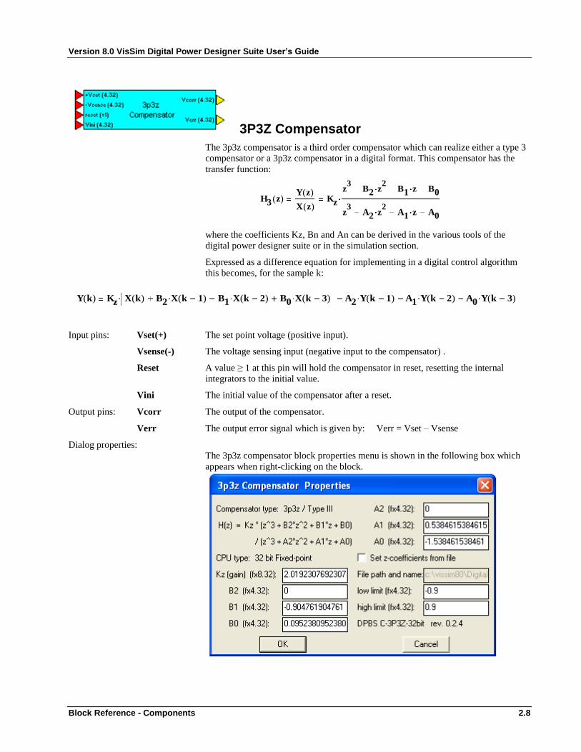
3P3Z Compensator
The 3p3z compensator is a third order compensator which can realize either a type 3
compensator or a 3p3z compensator in a digital format. This compensator has the
transfer function:
where the coefficients Kz, Bn and An can be derived in the various tools of the
digital power designer suite or in the simulation section.
Expressed as a difference equation for implementing in a digital control algorithm
this becomes, for the sample k:
Input pins: Vset(+) The set point voltage (positive input).
Vsense(-) The voltage sensing input (negative input to the compensator) .
Reset A value ≥ 1 at this pin will hold the compensator in reset, resetting the internal
integrators to the initial value.
Vini The initial value of the compensator after a reset.
Output pins: Vcorr The output of the compensator.
Verr The output error signal which is given by: Verr = Vset – Vsense
Dialog properties:
The 3p3z compensator block properties menu is shown in the following box which
appears when right-clicking on the block.
H3 z( )Y z( )
X z( )Kz
z3
B2 z2
B1 z B0
z3
A2 z2
A1 z A0
Y k( ) Kz X k( ) B2 X k 1( ) B1 X k 2( ) B0 X k 3( ) A2 Y k 1( ) A1 Y k 2( ) A0 Y k 3( )
Version 8.0 VisSim Digital Power Designer Suite User’s Guide
2.9 Block Reference - Components
Kz (gain):
Enter the DC gain of the compensator.
B2:
Enter the value of the second order numerator coefficient.
B1:
Enter the value of the first order numerator coefficient.
B0:
Enter the value of the lowest order numerator coefficient.
A2:
Enter the value of the second order denominator coefficient.
A1:
Enter the value of the first order denominator coefficient.
A0:
Enter the value of the lowest order denominator coefficient.
Set z-coefficients from file:
Check this box to read the z-coefficients from an external file.
File path and name:
Enter the full file name and path if selected.
Low limit:
Enter the high level limit of the compensator.
High limit:
Enter the low-level limit of the compensator.
NOTE that these limits are anti-windup limits.
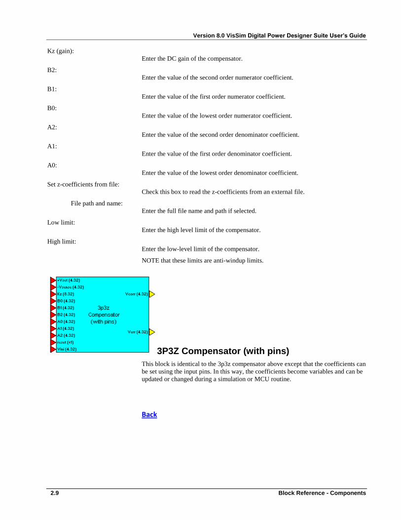
3P3Z Compensator (with pins)
This block is identical to the 3p3z compensator above except that the coefficients can
be set using the input pins. In this way, the coefficients become variables and can be
updated or changed during a simulation or MCU routine.
Back
Version 8.0 VisSim Digital Power Designer Suite User’s Guide
Block Reference - Components 2.10
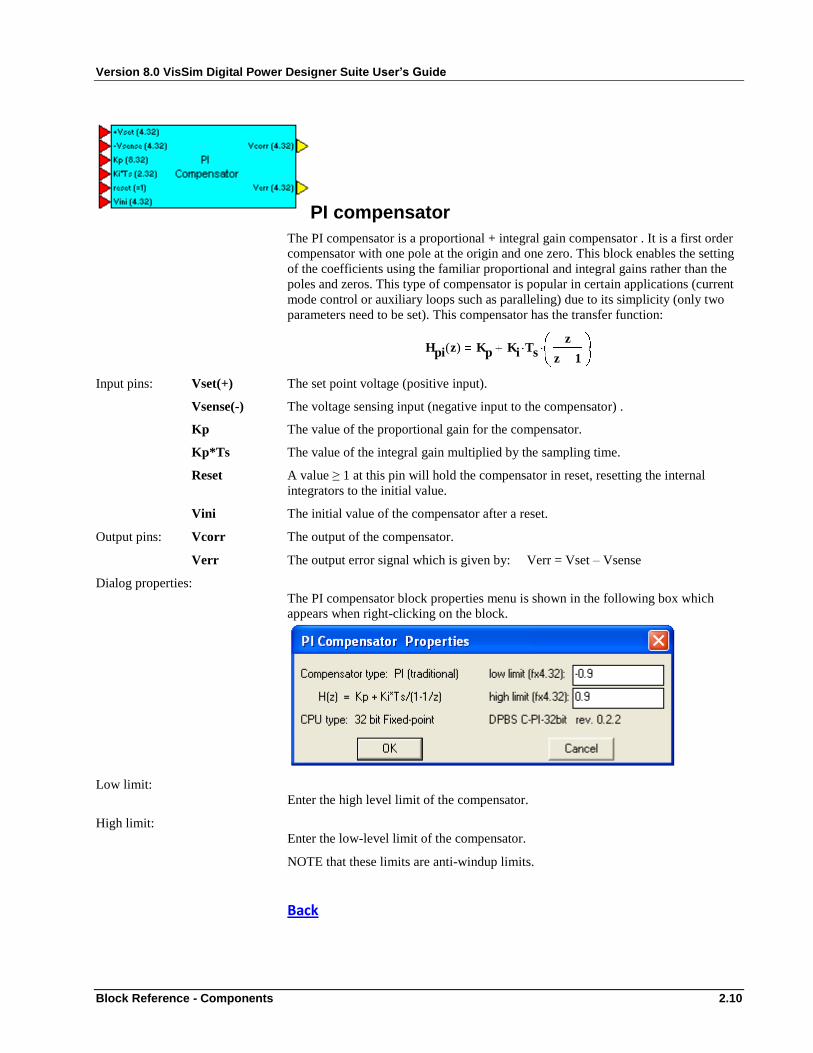
PI compensator
The PI compensator is a proportional + integral gain compensator . It is a first order
compensator with one pole at the origin and one zero. This block enables the setting
of the coefficients using the familiar proportional and integral gains rather than the
poles and zeros. This type of compensator is popular in certain applications (current
mode control or auxiliary loops such as paralleling) due to its simplicity (only two
parameters need to be set). This compensator has the transfer function:
Input pins: Vset(+) The set point voltage (positive input).
Vsense(-) The voltage sensing input (negative input to the compensator) .
Kp The value of the proportional gain for the compensator.
Kp*Ts The value of the integral gain multiplied by the sampling time.
Reset A value ≥ 1 at this pin will hold the compensator in reset, resetting the internal
integrators to the initial value.
Vini The initial value of the compensator after a reset.
Output pins: Vcorr The output of the compensator.
Verr The output error signal which is given by: Verr = Vset – Vsense
Dialog properties:
The PI compensator block properties menu is shown in the following box which
appears when right-clicking on the block.
Low limit:
Enter the high level limit of the compensator.
High limit:
Enter the low-level limit of the compensator.
NOTE that these limits are anti-windup limits.
Back
Hpi z( ) Kp Ki Tsz
z 1
Version 8.0 VisSim Digital Power Designer Suite User’s Guide
2.11 Block Reference - Components
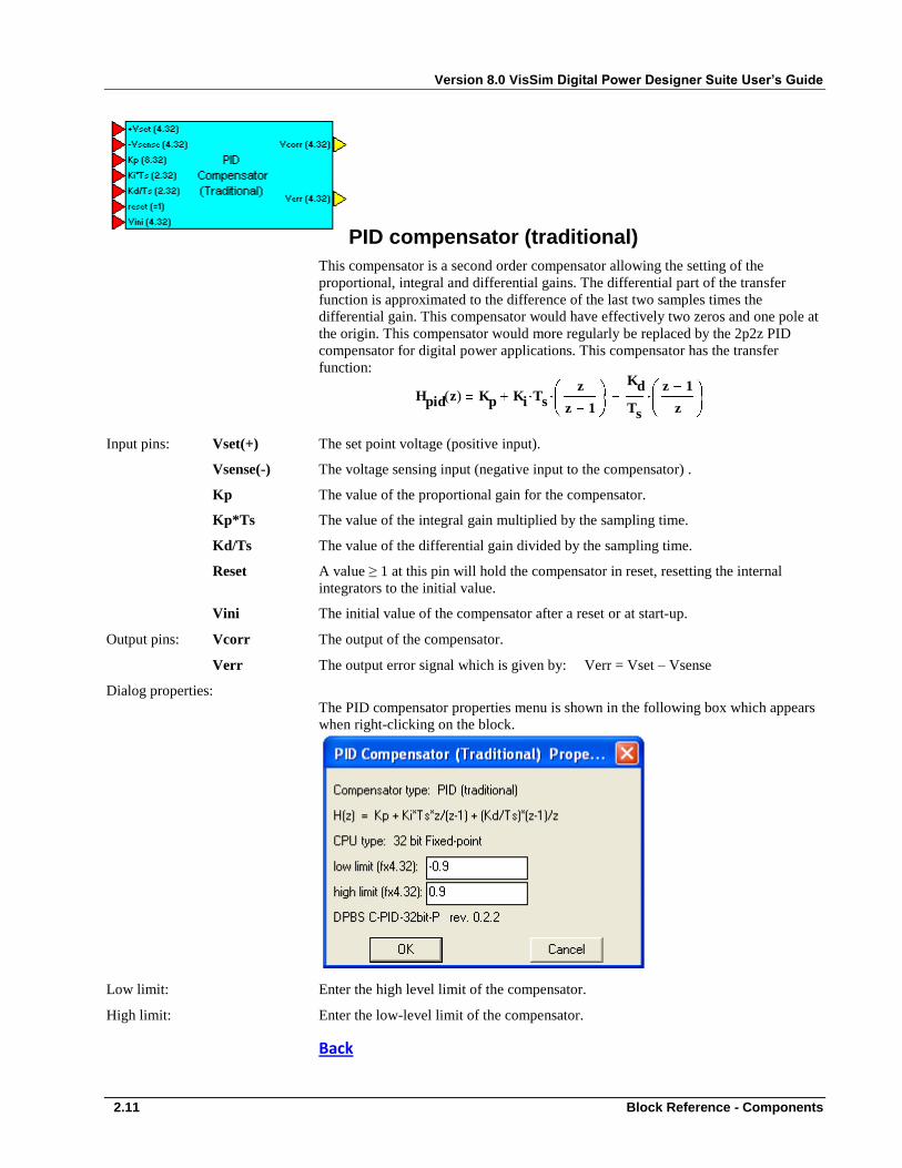
PID compensator (traditional)
This compensator is a second order compensator allowing the setting of the
proportional, integral and differential gains. The differential part of the transfer
function is approximated to the difference of the last two samples times the
differential gain. This compensator would have effectively two zeros and one pole at
the origin. This compensator would more regularly be replaced by the 2p2z PID
compensator for digital power applications. This compensator has the transfer
function:
Input pins: Vset(+) The set point voltage (positive input).
Vsense(-) The voltage sensing input (negative input to the compensator) .
Kp The value of the proportional gain for the compensator.
Kp*Ts The value of the integral gain multiplied by the sampling time.
Kd/Ts The value of the differential gain divided by the sampling time.
Reset A value ≥ 1 at this pin will hold the compensator in reset, resetting the internal
integrators to the initial value.
Vini The initial value of the compensator after a reset or at start-up.
Output pins: Vcorr The output of the compensator.
Verr The output error signal which is given by: Verr = Vset – Vsense
Dialog properties:
The PID compensator properties menu is shown in the following box which appears
when right-clicking on the block.
Low limit: Enter the high level limit of the compensator.
High limit: Enter the low-level limit of the compensator.
Back
Hpid z( ) Kp Ki Tsz
z 1
Kd
Ts
z 1
z

Version 8.0 VisSim Digital Power Designer Suite User’s Guide
Block Reference - Components 2.12
Controllers
Controllers are generally used in conjunction with the compensators to perform the
major part of digital power control loops for various control techniques. The time
slicer is an exception here which is used to control the time frame for the execution
of various tasks.
Time slicer
The time slicer controller performs time division multiplexing, first by two and
additionally by four.
Output pins: TS0 Time divided by 2; first interval.
TS1 Time divided by 2; second interval.
TS00 Time divided by 4; first interval.
TS01 Time divided by 4; second interval.
TS10 Time divided by 4; third interval.
TS11 Time divided by 4; fourth interval.
The time intervals are represented in the following graph.
Version 8.0 VisSim Digital Power Designer Suite User’s Guide
2.13 Block Reference - Components
If a task does not need to run at the full ISR rate then its rate can be divided down by
an integer number of the ISR rate. If several tasks are to be run at the divided down
rate, then simply setting them to the same rate can create problems with CPU usage
as the various tasks will be executed during the same ISR time frame, perhaps
overloading the CPU with tasks in that frame while during other time frames, the
CPU will be relatively free. This situation can be avoided with time slicing so that
the task execution is more evenly distributed over time.
The time slicer would be normally connected up in a diagram similar to the
following:
Without time-slicing, the tasks, which would then each be chosen to run at a larger
local time step in the compound block properties, would all be executed together
during the time frame TS00, perhaps burdening too much the CPU during this ISR
cycle while the next three ISR cycles have execution time in reserve. With time-
slicing, the four tasks (especially if identical in execution time), will be executed
with a more even distribution over time and possibly allowing for additional tasks to
be included in the routine at the full ISR rate.
Back
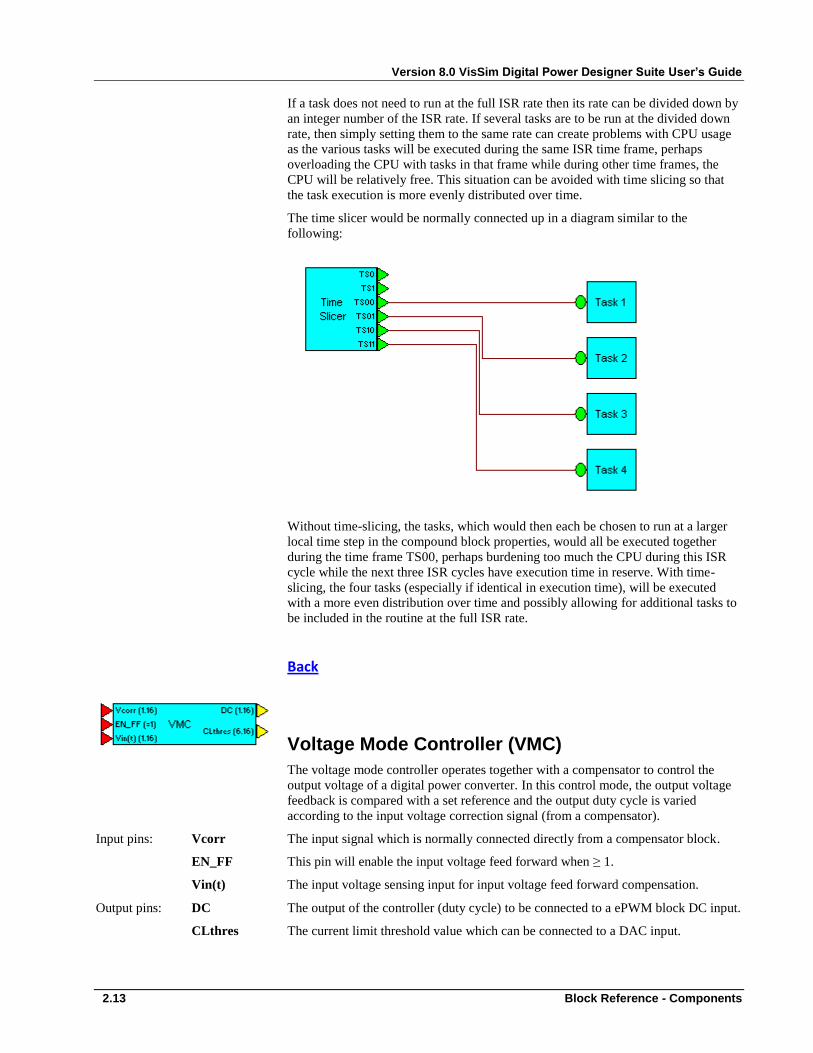
Voltage Mode Controller (VMC)
The voltage mode controller operates together with a compensator to control the
output voltage of a digital power converter. In this control mode, the output voltage
feedback is compared with a set reference and the output duty cycle is varied
according to the input voltage correction signal (from a compensator).
Input pins: Vcorr The input signal which is normally connected directly from a compensator block.
EN_FF This pin will enable the input voltage feed forward when ≥ 1.
Vin(t) The input voltage sensing input for input voltage feed forward compensation.
Output pins: DC The output of the controller (duty cycle) to be connected to a ePWM block DC input.
CLthres The current limit threshold value which can be connected to a DAC input.
Version 8.0 VisSim Digital Power Designer Suite User’s Guide
Block Reference - Components 2.14
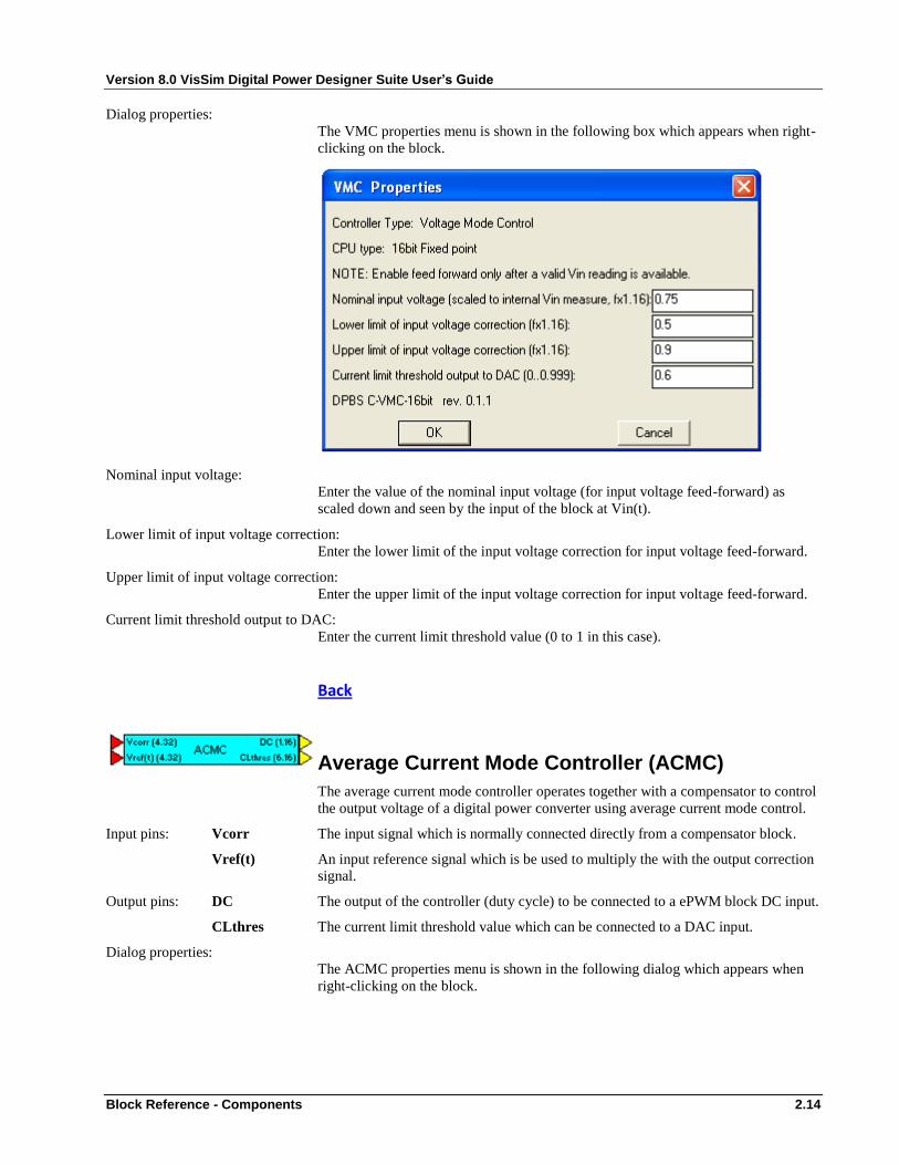
Dialog properties:
The VMC properties menu is shown in the following box which appears when right-
clicking on the block.
Nominal input voltage:
Enter the value of the nominal input voltage (for input voltage feed-forward) as
scaled down and seen by the input of the block at Vin(t).
Lower limit of input voltage correction:
Enter the lower limit of the input voltage correction for input voltage feed-forward.
Upper limit of input voltage correction:
Enter the upper limit of the input voltage correction for input voltage feed-forward.
Current limit threshold output to DAC:
Enter the current limit threshold value (0 to 1 in this case).
Back
Average Current Mode Controller (ACMC)
The average current mode controller operates together with a compensator to control
the output voltage of a digital power converter using average current mode control.
Input pins: Vcorr The input signal which is normally connected directly from a compensator block.
Vref(t) An input reference signal which is be used to multiply the with the output correction
signal.
Output pins: DC The output of the controller (duty cycle) to be connected to a ePWM block DC input.
CLthres The current limit threshold value which can be connected to a DAC input.
Dialog properties:
The ACMC properties menu is shown in the following dialog which appears when
right-clicking on the block.
Version 8.0 VisSim Digital Power Designer Suite User’s Guide
2.15 Block Reference - Components
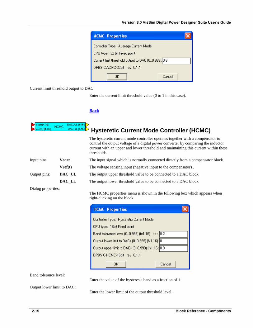
Current limit threshold output to DAC:
Enter the current limit threshold value (0 to 1 in this case).
Back
Hysteretic Current Mode Controller (HCMC)
The hysteretic current mode controller operates together with a compensator to
control the output voltage of a digital power converter by comparing the inductor
current with an upper and lower threshold and maintaining this current within these
thresholds.
Input pins: Vcorr The input signal which is normally connected directly from a compensator block.
Vref(t) The voltage sensing input (negative input to the compensator) .
Output pins: DAC_UL The output upper threshold value to be connected to a DAC block.
DAC_LL The output lower threshold value to be connected to a DAC block.
Dialog properties:
The HCMC properties menu is shown in the following box which appears when
right-clicking on the block.
Band tolerance level:
Enter the value of the hysteresis band as a fraction of 1.
Output lower limit to DAC:
Enter the lower limit of the output threshold level.
Version 8.0 VisSim Digital Power Designer Suite User’s Guide
Block Reference - Components 2.16
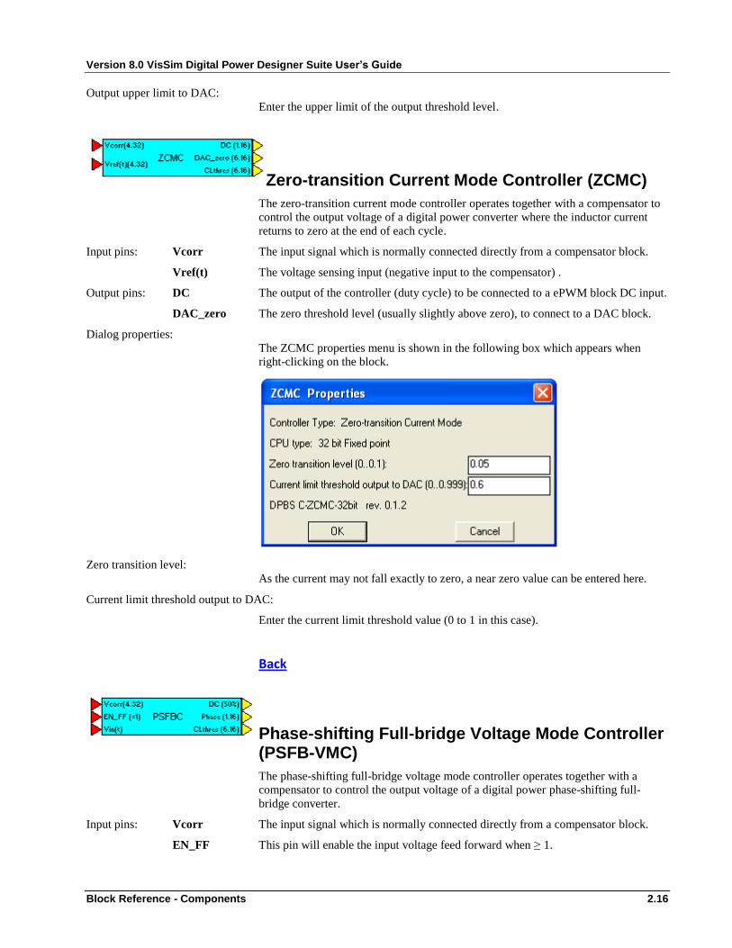
Output upper limit to DAC:
Enter the upper limit of the output threshold level.
Zero-transition Current Mode Controller (ZCMC)
The zero-transition current mode controller operates together with a compensator to
control the output voltage of a digital power converter where the inductor current
returns to zero at the end of each cycle.
Input pins: Vcorr The input signal which is normally connected directly from a compensator block.
Vref(t) The voltage sensing input (negative input to the compensator) .
Output pins: DC The output of the controller (duty cycle) to be connected to a ePWM block DC input.
DAC_zero The zero threshold level (usually slightly above zero), to connect to a DAC block.
Dialog properties:
The ZCMC properties menu is shown in the following box which appears when
right-clicking on the block.
Zero transition level:
As the current may not fall exactly to zero, a near zero value can be entered here.
Current limit threshold output to DAC:
Enter the current limit threshold value (0 to 1 in this case).
Back
Phase-shifting Full-bridge Voltage Mode Controller (PSFB-VMC)
The phase-shifting full-bridge voltage mode controller operates together with a
compensator to control the output voltage of a digital power phase-shifting full-
bridge converter.
Input pins: Vcorr The input signal which is normally connected directly from a compensator block.
EN_FF This pin will enable the input voltage feed forward when ≥ 1.

Version 8.0 VisSim Digital Power Designer Suite User’s Guide
2.17 Block Reference - Components
Vin(t) The voltage sensing input (negative input to the compensator)
Output pins: DC This output is simply a fixed 50% duty cycle output which can be connected to two
ePWM blocks DC input.
Phase The output of the controller which can be connected to one of the two ePWM blocks
to control the relative phase between the PWMs.
CLthres The current limit threshold value which can be connected to a DAC input.
Dialog properties:
The PSFB-VMC properties menu is shown in the following box which appears when
right-clicking on the block
Nominal input voltage:
Enter the value of the nominal input voltage (for input voltage feed-forward) as
scaled down and seen by the input of the block at Vin(t).
Lower limit of phase shift:
Enter the lower limit of the phase value for phase-shifting control.
Upper limit of phase shift:
Enter the upper limit of the phase value for phase-shifting control.
Lower limit of input voltage correction:
Enter the lower limit of the input voltage correction for input voltage feed-forward.
Upper limit of input voltage correction:
Enter the upper limit of the input voltage correction for input voltage feed-forward.
Current limit threshold output to DAC
Enter the current limit threshold value (0 to 1 in this case).
Back
Version 8.0 VisSim Digital Power Designer Suite User’s Guide
Block Reference - Components 2.18
Filters
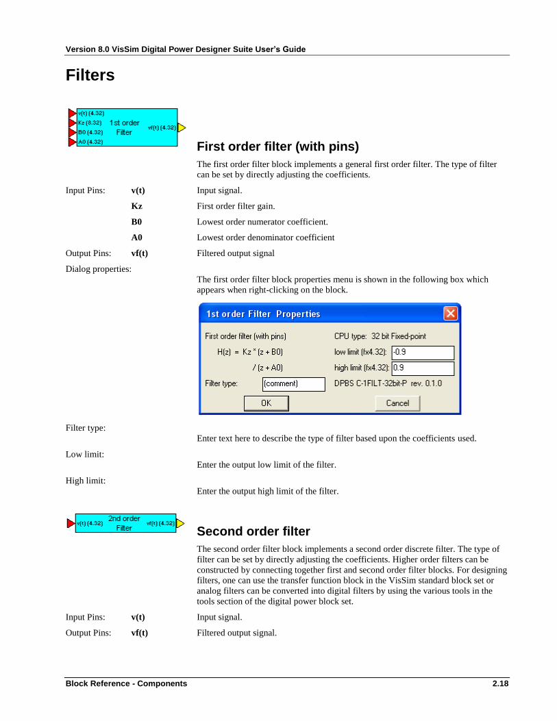
First order filter (with pins)
The first order filter block implements a general first order filter. The type of filter
can be set by directly adjusting the coefficients.
Input Pins: v(t) Input signal.
Kz First order filter gain.
B0 Lowest order numerator coefficient.
A0 Lowest order denominator coefficient
Output Pins: vf(t) Filtered output signal
Dialog properties:
The first order filter block properties menu is shown in the following box which
appears when right-clicking on the block.
Filter type:
Enter text here to describe the type of filter based upon the coefficients used.
Low limit:
Enter the output low limit of the filter.
High limit:
Enter the output high limit of the filter.
Second order filter
The second order filter block implements a second order discrete filter. The type of
filter can be set by directly adjusting the coefficients. Higher order filters can be
constructed by connecting together first and second order filter blocks. For designing
filters, one can use the transfer function block in the VisSim standard block set or
analog filters can be converted into digital filters by using the various tools in the
tools section of the digital power block set.
Input Pins: v(t) Input signal.
Output Pins: vf(t) Filtered output signal.

Version 8.0 VisSim Digital Power Designer Suite User’s Guide
2.19 Block Reference - Components
Dialog properties:
The second order filter block properties menu is shown in the following box which
appears when right-clicking on the block.
Filter type:
The choices here are:
Kz (gain):
Enter the DC gain of the compensator.
B1:
Enter the value of the first order numerator coefficient.
B0:
Enter the value of the lowest order numerator coefficient.
A1:
Enter the value of the first order denominator coefficient.
A0:
Enter the value of the lowest order denominator coefficient.
Set coefficients from file:
Check this box to read the coefficients from an external file.
File path and name:
Enter the complete file name and path for the location of the file.
Low limit:
Enter the output low limit of the filter.
High limit:
Enter the output high limit of the filter.
Back

Version 8.0 VisSim Digital Power Designer Suite User’s Guide
Block Reference - Components 2.20
Second order filter (with pins)
This filter block is identical to the second order filter except that the coefficients can
be set with input pins.
Input Pins: v(t) Input signal.
Output Pins: vf(t) Filtered output signal.
Dialog properties:
The second order filter block properties menu is shown in the following box which
appears when right-clicking on the block.
Filter type:
Enter text here to describe the type of filter based upon the coefficients used.
Low limit:
Enter the output low limit of the filter.
High limit:
Enter the output high limit of the filter.
Back
Moving average filter
The moving average filter as realized here updates at every time step by sampling the
current input and passing the past samples through the filter similar to a FIFO. If the
samples are all equal then it is a simple average of the most recent samples.
The moving average filter from the simulation section of the digital power block set
can be used to generate the coefficients for simple, linear and exponential types of
moving average.
Input Pins: v(t) Input signal.
Output Pins: vf(t) Filtered output signal.

Version 8.0 VisSim Digital Power Designer Suite User’s Guide
2.21 Block Reference - Components
Dialog properties:
The moving average filter block properties menu is shown in the following box
which appears when right-clicking on the block.
Filter type:
There are two Moving Average Filter blocks in the block set with filter orders of
either 4 or 10 step.
Filter DC Gain Multiplier:
Enter the required DC gain multiplier of the filter. Note that this is not the DC gain
of the filter but rather a multiplier to adapt the DC gain.
Coefficient B0:
Enter the multiplier for the current sample.
Coefficient B1:
Enter the multiplier for the past sample.
Coefficient B2:
Enter the multiplier for the z-2
sample.
.
.
.
Coefficient B9:
Enter the multiplier for the oldest sample (z-9
in this case).
Output low limit:
The output can be limited to this minimum value.
Output high limit:
The output can be limited to this maximum value.
Back

Version 8.0 VisSim Digital Power Designer Suite User’s Guide
Block Reference - Components 2.22
Moving median filter
The moving median filter takes the median value of an input sample. In this
particular realization, 4 samples are used so that the minimum and maximum values
are ignored, leaving the two median values which are then averaged to form the
output value. Similar blocks can be found in the VisSim main block set under:
blocks matrix operation meanSmooth and medianSmooth.
Input Pins: In Input signal.
Output Pins: Out Filtered output signal.
Back
Version 8.0 VisSim Digital Power Designer Suite User’s Guide
2.23 Block Reference - Components
Measurements
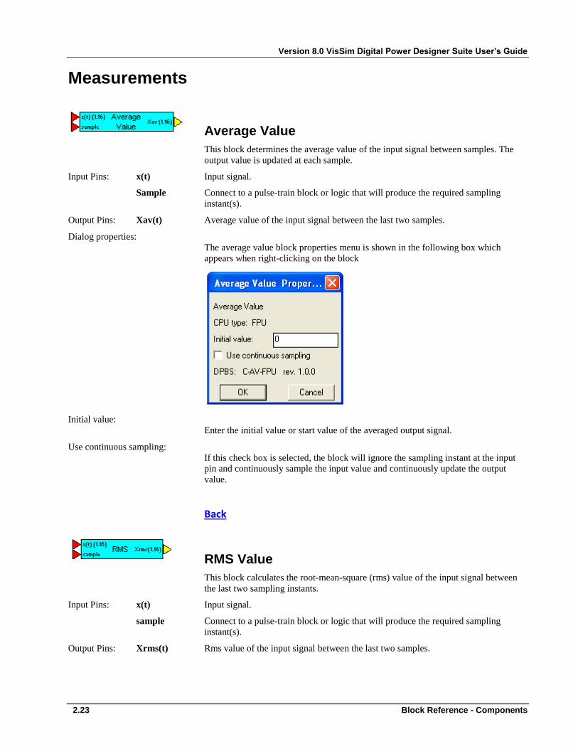
Average Value
This block determines the average value of the input signal between samples. The
output value is updated at each sample.
Input Pins: x(t) Input signal.
Sample Connect to a pulse-train block or logic that will produce the required sampling
instant(s).
Output Pins: Xav(t) Average value of the input signal between the last two samples.
Dialog properties:
The average value block properties menu is shown in the following box which
appears when right-clicking on the block
Initial value:
Enter the initial value or start value of the averaged output signal.
Use continuous sampling:
If this check box is selected, the block will ignore the sampling instant at the input
pin and continuously sample the input value and continuously update the output
value.
Back
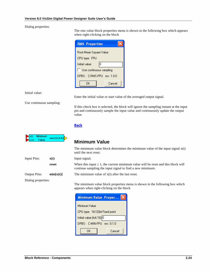
RMS Value
This block calculates the root-mean-square (rms) value of the input signal between
the last two sampling instants.
Input Pins: x(t) Input signal.
sample Connect to a pulse-train block or logic that will produce the required sampling
instant(s).
Output Pins: Xrms(t) Rms value of the input signal between the last two samples.
Version 8.0 VisSim Digital Power Designer Suite User’s Guide
Block Reference - Components 2.24
Dialog properties:
The rms value block properties menu is shown in the following box which appears
when right-clicking on the block
Initial value:
Enter the initial value or start value of the averaged output signal.
Use continuous sampling:
If this check box is selected, the block will ignore the sampling instant at the input
pin and continuously sample the input value and continuously update the output
value.
Back
Minimum Value
The minimum value block determines the minimum value of the input signal x(t)
until the next reset.
Input Pins: x(t) Input signal.
reset When this input ≥ 1, the current minimum value will be reset and this block will
continue sampling the input signal to find a new minimum.
Output Pins: min[x(t)] The minimum value of x(t) after the last reset.
Dialog properties:
The minimum value block properties menu is shown in the following box which
appears when right-clicking on the block
Version 8.0 VisSim Digital Power Designer Suite User’s Guide
2.25 Block Reference - Components
Initial value:
Enter the desired initial value for the minimum value determination.
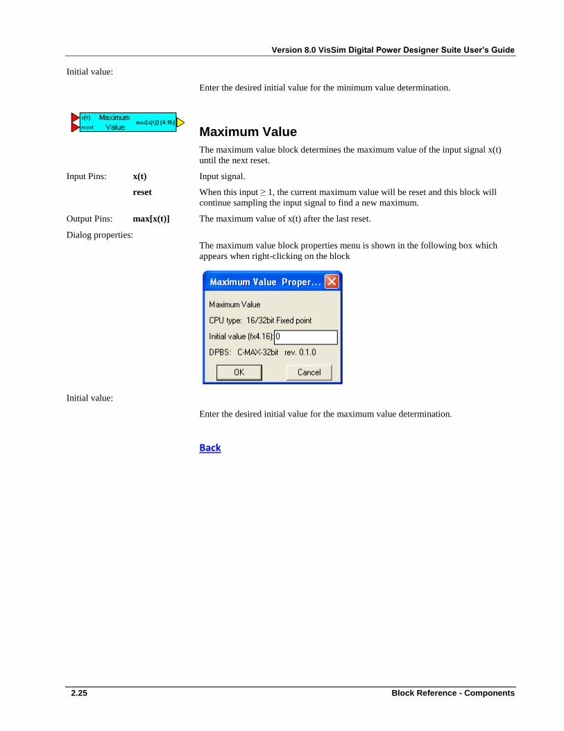
Maximum Value
The maximum value block determines the maximum value of the input signal x(t)
until the next reset.
Input Pins: x(t) Input signal.
reset When this input ≥ 1, the current maximum value will be reset and this block will
continue sampling the input signal to find a new maximum.
Output Pins: max[x(t)] The maximum value of x(t) after the last reset.
Dialog properties:
The maximum value block properties menu is shown in the following box which
appears when right-clicking on the block
Initial value:
Enter the desired initial value for the maximum value determination.
Back

Version 8.0 VisSim Digital Power Designer Suite User’s Guide
Block Reference - Components 2.26
Real Power
This block will calculate the real power, given the time dependent voltage and
current input signals by taking the average value of p(t) where p(t) is given by:
p(t) = v(t)*i(t)
and then:
Input Pins: v(t) Time-varying voltage input.
i(t) Time-varying current input.
sample Connect to a pulse-train block or logic that will produce the required sampling
instant(s).
Output Pins: P The real power output.
Dialog properties:
The real power block properties menu is shown in the following box which appears
when right-clicking on the block
Initial value:
Enter the initial value or start value of the averaged output signal.
Use continuous sampling:
If this check box is selected, the block will ignore the sampling instant at the input
pin and continuously sample the input value and continuously update the output
value.
Back
P1
mn
n m
k
pk t( )

Version 8.0 VisSim Digital Power Designer Suite User’s Guide
2.27 Block Reference - Components
Reactive Power
This block will calculate the reactive power, given the apparent power and real
power input signals The reactive power is then given by:
Input Pins: VA Apparent power input.
P Real power input.
Output Pins: Q The reactive power output.
Apparent Power
This block calculates the apparent power based upon the time-varying system
voltage and current.
Input Pins: v(t) Time-varying voltage input.
i(t) Time-varying current input.
sample Connect to a pulse-train block or logic that will produce the required sampling
instant(s).
Output Pins: VA The apparent power output.
Dialog properties:
The apparent power block properties menu is shown in the following box which
appears when right-clicking on the block.
Initial value:
Enter the initial value or start value of the averaged output signal.
Use continuous sampling:
If this check box is selected, the block will ignore the sampling instant at the input
pin and continuously sample the input value and continuously update the output
value.
Q VA2
P2

Version 8.0 VisSim Digital Power Designer Suite User’s Guide
Block Reference - Components 2.28
Power Factor
This block calculates the power factor as:
Input Pins: VA Apparent power input.
P Real power input.
Output Pins: PF The power factor output.
Crest Factor
The Crest Factor block measures the crest factor of the input signal. i.e.
Input Pins: x(t) Input signal.
sample Connect to a pulse-train block or logic that will produce the required sampling
instant(s).
Output Pins: CF The crest factor of the input signal measured between the last two samples.
Dialog properties:
The crest factor block properties menu is shown in the following box which appears
when right-clicking on the block.
Initial value:
Enter the initial value or start value of the averaged output signal.
Use continuous sampling:
If this check box is selected, the block will ignore the sampling instant at the input
pin and continuously sample the input value and continuously update the output
value.
Back
PFP
VA
CFmax x t( )( )
Xrms
Version 8.0 VisSim Digital Power Designer Suite User’s Guide
2.29 Block Reference - Components
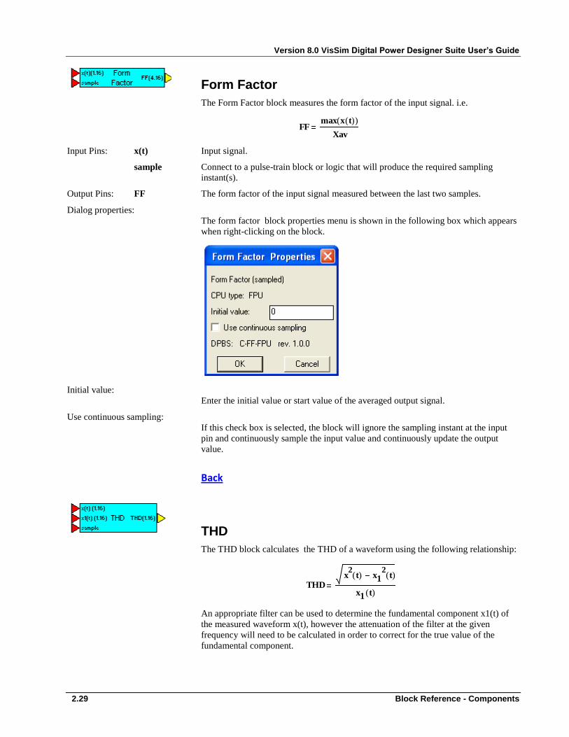
Form Factor
The Form Factor block measures the form factor of the input signal. i.e.
Input Pins: x(t) Input signal.
sample Connect to a pulse-train block or logic that will produce the required sampling
instant(s).
Output Pins: FF The form factor of the input signal measured between the last two samples.
Dialog properties:
The form factor block properties menu is shown in the following box which appears
when right-clicking on the block.
Initial value:
Enter the initial value or start value of the averaged output signal.
Use continuous sampling:
If this check box is selected, the block will ignore the sampling instant at the input
pin and continuously sample the input value and continuously update the output
value.
Back
THD
The THD block calculates the THD of a waveform using the following relationship:
An appropriate filter can be used to determine the fundamental component x1(t) of
the measured waveform x(t), however the attenuation of the filter at the given
frequency will need to be calculated in order to correct for the true value of the
fundamental component.
FFmax x t( )( )
Xav
THDx
2t( ) x1
2t( )
x1 t( )

Version 8.0 VisSim Digital Power Designer Suite User’s Guide
Block Reference - Components 2.30
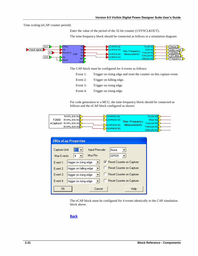
Time - Frequency
The time-frequency measurement block functions together with an Event Capture
block from the simulation section or with an eCAP block from the VisSim ECD
Embedded section.
Input Pins: eCAPx The captured timer output values of the CAP block (simulation) or eCAP block
(VisSim embedded) .
Output Pins: T(s) The period of the input signal in seconds, based upon the captured timer values.
DC The duty cycle of the input signal, based upon the captured timer values.
Ton (s) The ON time of the input signal in seconds, based upon the captured timer values.
Toff (s) The OFF time of the input signal in seconds, based upon the captured timer values.
F (Hz) The frequency of the input signal in Hertz, based upon the captured timer values.
Dialog properties:
The time-frequency block properties menu is shown in the following box which
appears when right-clicking on the block.
Version 8.0 VisSim Digital Power Designer Suite User’s Guide
2.31 Block Reference - Components
Time scaling (eCAP counter period):
Enter the value of the period of the 32-bit counter (1/SYSCLKOUT).
The time-frequency block should be connected as follows in a simulation diagram:
The CAP block must be configured for 4 events as follows:
Event 1: Trigger on rising edge and reset the counter on this capture event.
Event 2: Trigger on falling edge.
Event 3: Trigger on rising edge.
Event 4: Trigger on rising edge.
For code generation to a MCU, the time-frequency block should be connected as
follows and the eCAP block configured as shown:
The eCAP block must be configured for 4 events identically to the CAP simulation
block above.
Back
Version 8.0 VisSim Digital Power Designer Suite User’s Guide
Block Reference - Components 2.32
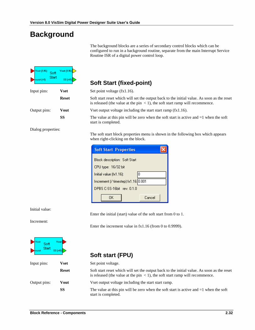
Background
The background blocks are a series of secondary control blocks which can be
configured to run in a background routine, separate from the main Interrupt Service
Routine ISR of a digital power control loop.
Soft Start (fixed-point)
Input pins: Vset Set point voltage (fx1.16).
Reset Soft start reset which will set the output back to the initial value. As soon as the reset
is released (the value at the pin < 1), the soft start ramp will recommence.
Output pins: Vout Vset output voltage including the start start ramp (fx1.16).
SS The value at this pin will be zero when the soft start is active and =1 when the soft
start is completed.
Dialog properties:
The soft start block properties menu is shown in the following box which appears
when right-clicking on the block.
Initial value:
Enter the initial (start) value of the soft start from 0 to 1.
Increment:
Enter the increment value in fx1.16 (from 0 to 0.9999).
Soft start (FPU)
Input pins: Vset Set point voltage.
Reset Soft start reset which will set the output back to the initial value. As soon as the reset
is released (the value at the pin < 1), the soft start ramp will recommence.
Output pins: Vout Vset output voltage including the start start ramp.
SS The value at this pin will be zero when the soft start is active and =1 when the soft
start is completed.
Version 8.0 VisSim Digital Power Designer Suite User’s Guide
2.33 Block Reference - Components
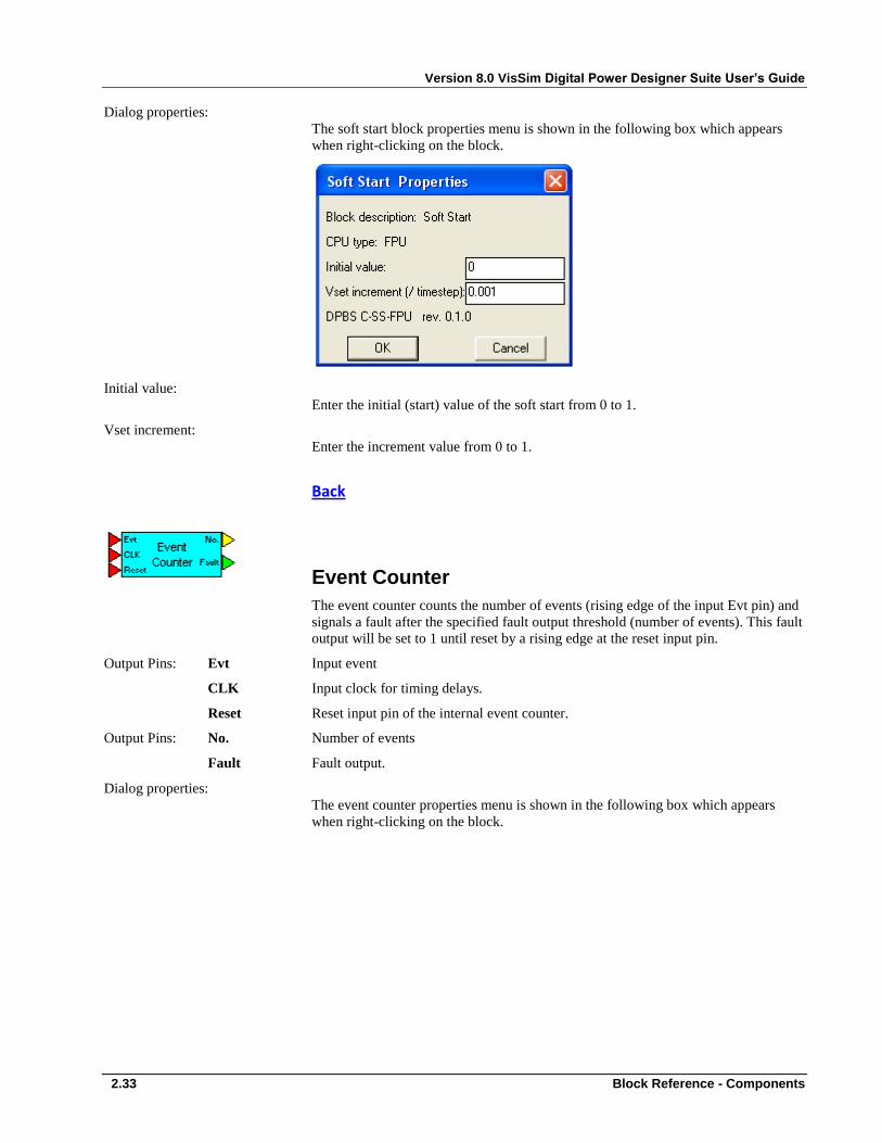
Dialog properties:
The soft start block properties menu is shown in the following box which appears
when right-clicking on the block.
Initial value:
Enter the initial (start) value of the soft start from 0 to 1.
Vset increment:
Enter the increment value from 0 to 1.
Back
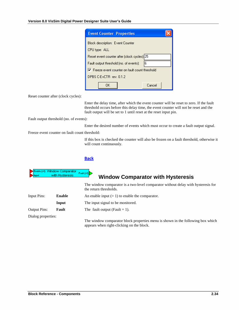
Event Counter
The event counter counts the number of events (rising edge of the input Evt pin) and
signals a fault after the specified fault output threshold (number of events). This fault
output will be set to 1 until reset by a rising edge at the reset input pin.
Output Pins: Evt Input event
CLK Input clock for timing delays.
Reset Reset input pin of the internal event counter.
Output Pins: No. Number of events
Fault Fault output.
Dialog properties:
The event counter properties menu is shown in the following box which appears
when right-clicking on the block.
Version 8.0 VisSim Digital Power Designer Suite User’s Guide
Block Reference - Components 2.34
Reset counter after (clock cycles):
Enter the delay time, after which the event counter will be reset to zero. If the fault
threshold occurs before this delay time, the event counter will not be reset and the
fault output will be set to 1 until reset at the reset input pin.
Fault output threshold (no. of events):
Enter the desired number of events which must occur to create a fault output signal.
Freeze event counter on fault count threshold:
If this box is checked the counter will also be frozen on a fault threshold, otherwise it
will count continuously.
Back
Window Comparator with Hysteresis
The window comparator is a two-level comparator without delay with hysteresis for
the return thresholds.
Input Pins: Enable An enable input (= 1) to enable the comparator.
Input The input signal to be monitored.
Output Pins: Fault The fault output (Fault = 1).
Dialog properties:
The window comparator block properties menu is shown in the following box which
appears when right-clicking on the block.
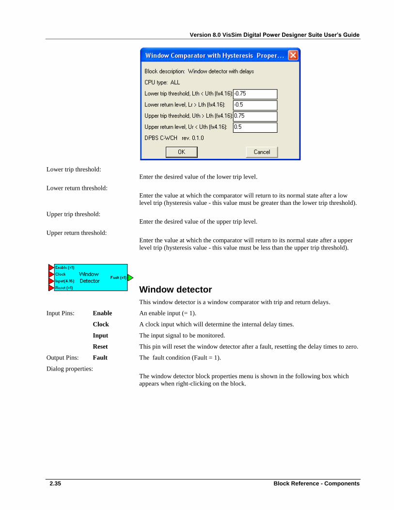
Version 8.0 VisSim Digital Power Designer Suite User’s Guide
2.35 Block Reference - Components
Lower trip threshold:
Enter the desired value of the lower trip level.
Lower return threshold:
Enter the value at which the comparator will return to its normal state after a low
level trip (hysteresis value - this value must be greater than the lower trip threshold).
Upper trip threshold:
Enter the desired value of the upper trip level.
Upper return threshold:
Enter the value at which the comparator will return to its normal state after a upper
level trip (hysteresis value - this value must be less than the upper trip threshold).
Window detector
This window detector is a window comparator with trip and return delays.
Input Pins: Enable An enable input (= 1).
Clock A clock input which will determine the internal delay times.
Input The input signal to be monitored.
Reset This pin will reset the window detector after a fault, resetting the delay times to zero.
Output Pins: Fault The fault condition (Fault = 1).
Dialog properties:
The window detector block properties menu is shown in the following box which
appears when right-clicking on the block.

Version 8.0 VisSim Digital Power Designer Suite User’s Guide
Block Reference - Components 2.36
Lower trip threshold:
Enter the desired value of the lower trip level.
Upper threshold:
Enter the desired value of the upper trip level.
Fault activation delay (clock periods):
Enter the delay time of the fault activation. For a fault to be activated (output = 1),
the input level must remain outside the trip levels for the duration of this delay.
Return delay (clock periods):
Enter the return delay time at which the output will return to normal (= 0). The input
level must remain within the two trip levels for the duration of this delay.
Back
Version 8.0 VisSim Digital Power Designer Suite User’s Guide
2.37 Block Reference - Components
Code-generable Control Loops
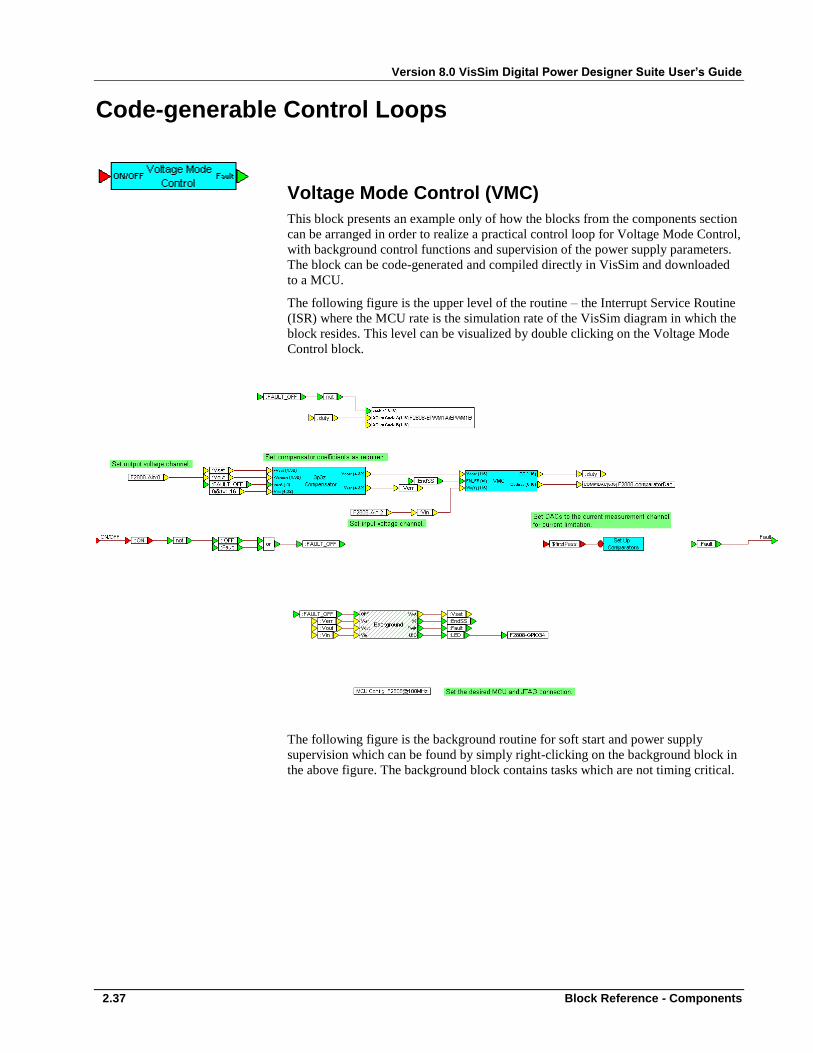
Voltage Mode Control (VMC)
This block presents an example only of how the blocks from the components section
can be arranged in order to realize a practical control loop for Voltage Mode Control,
with background control functions and supervision of the power supply parameters.
The block can be code-generated and compiled directly in VisSim and downloaded
to a MCU.
The following figure is the upper level of the routine – the Interrupt Service Routine
(ISR) where the MCU rate is the simulation rate of the VisSim diagram in which the
block resides. This level can be visualized by double clicking on the Voltage Mode
Control block.
The following figure is the background routine for soft start and power supply
supervision which can be found by simply right-clicking on the background block in
the above figure. The background block contains tasks which are not timing critical.
Version 8.0 VisSim Digital Power Designer Suite User’s Guide
Block Reference - Components 2.38
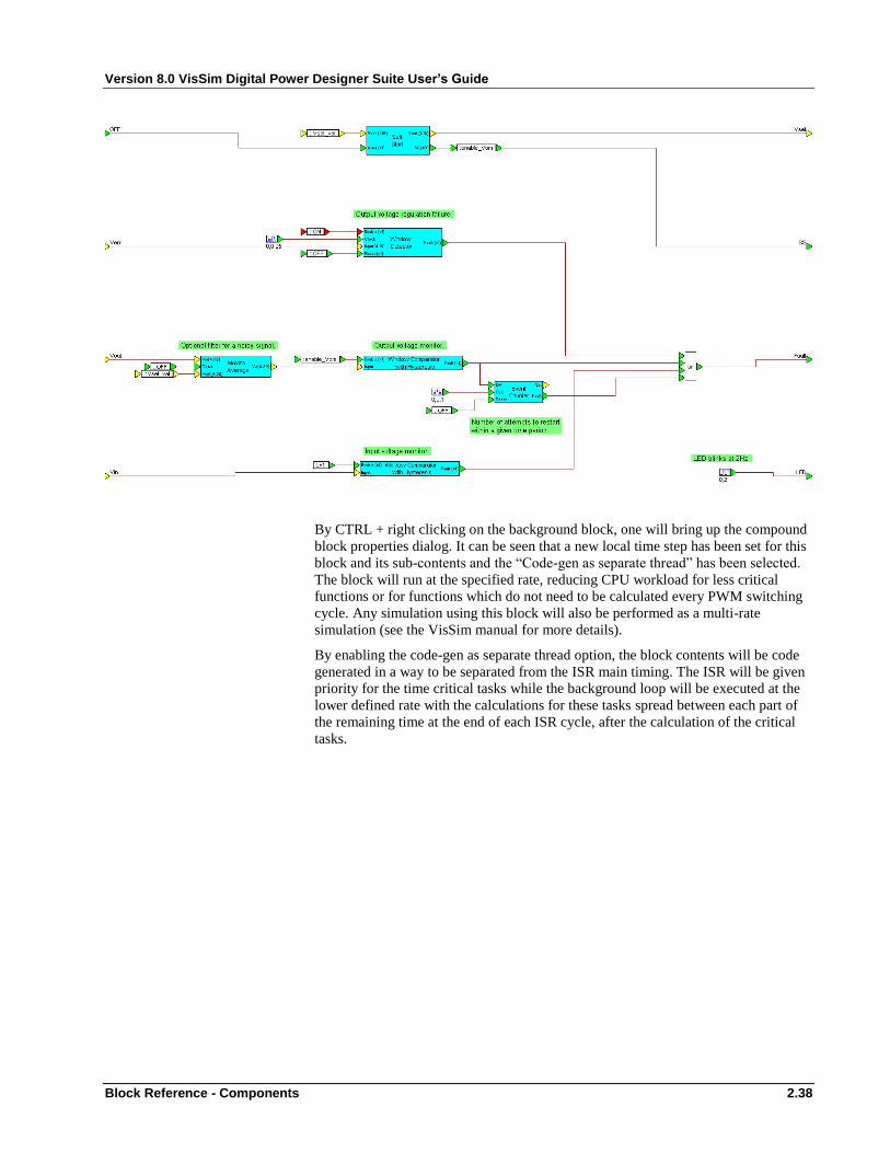
By CTRL + right clicking on the background block, one will bring up the compound
block properties dialog. It can be seen that a new local time step has been set for this
block and its sub-contents and the “Code-gen as separate thread” has been selected.
The block will run at the specified rate, reducing CPU workload for less critical
functions or for functions which do not need to be calculated every PWM switching
cycle. Any simulation using this block will also be performed as a multi-rate
simulation (see the VisSim manual for more details).
By enabling the code-gen as separate thread option, the block contents will be code
generated in a way to be separated from the ISR main timing. The ISR will be given
priority for the time critical tasks while the background loop will be executed at the
lower defined rate with the calculations for these tasks spread between each part of
the remaining time at the end of each ISR cycle, after the calculation of the critical
tasks.

Version 8.0 VisSim Digital Power Designer Suite User’s Guide
2.39 Block Reference - Components
Peak Current Mode Control (PCMC)
This block presents an example only of how the blocks from the components section
can be arranged in order to realize a practical control loop for Peak Current Mode
Control, with background control functions and supervision of the power supply
parameters. The block can be code-generated and compiled directly in VisSim and
downloaded to a MCU. The organisation of the blocks at the lower levels are similar
to the voltage mode control code generable block.
Average Current Mode Control (ACMC)
This block presents an example only of how the blocks from the components section
can be arranged in order to realize a practical control loop for Average Current Mode
Control, with background control functions and supervision of the power supply
parameters. The block can be code-generated and compiled directly in VisSim and
downloaded to a MCU. The organisation of the blocks at the lower levels are similar
to the voltage mode control code generable block.

Version 8.0 VisSim Digital Power Designer Suite User’s Guide
Block Reference - Components 2.40
Hysteretic Current Mode Control (HCMC)
This block presents an example only of how the blocks from the components section
can be arranged in order to realize a practical control loop for Hysteretic Current
Mode Control, with background control functions and supervision of the power
supply parameters. The block can be code-generated and compiled directly in
VisSim and downloaded to a MCU. The organisation of the blocks at the lower
levels are similar to the voltage mode control code generable block.
Zero-transition Current Mode Control (ZCMC)
This block presents an example only of how the blocks from the components section
can be arranged in order to realize a practical control loop for Zero-transition Current
Mode Control, with background control functions and supervision of the power
supply parameters. The block can be code-generated and compiled directly in
VisSim and downloaded to a MCU. The organisation of the blocks at the lower
levels are similar to the voltage mode control code generable block.
Phase Shifting Full-bridge Voltage Mode Control (PSFB-VMC)
This block presents an example only of how the blocks from the components section
can be arranged in order to realize a practical control loop for Phase-shifting Full-
bridge Voltage Mode Control, with background control functions and supervision of
the power supply parameters. The block can be code-generated and compiled
directly in VisSim and downloaded to a MCU. The organisation of the blocks at the
lower levels are similar to the voltage mode control code generable block.
Back

Version 8.0 VisSim Digital Power Designer Suite User’s Guide
2.41 Block Reference - Components
Frequently Used
This section of blocks within the components section consists of a set of freely
usable and modifiable blocks which are frequently used in developing digital control
algorithms. The blocks in this location can be added to by the user by simply saving
a diagram with the desired name into this directory.
Back
Chapter 3 - Contents
BLOCK REFERENCE - SIMULATION ......................................................................................................... 3
Block Convention .......................................................................................................................................................... 3
Customizing Blocks ....................................................................................................................................................... 4
Sources ......................................................................................................................................................................... 5 DC supply .......................................................................................................................................................................... 5 AC supply .......................................................................................................................................................................... 9 Three-phase AC supply ................................................................................................................................................... 14 Controlled AC supply ...................................................................................................................................................... 19 Controlled-slew AC supply .............................................................................................................................................. 19 Controlled-slew DC supply .............................................................................................................................................. 20 Simulation time .............................................................................................................................................................. 21
Sensors ....................................................................................................................................................................... 22 Resistive divider (voltage sense) ..................................................................................................................................... 22 Current sense resistor..................................................................................................................................................... 23 AC current transformer .................................................................................................................................................. 24 Isolated current sensor ................................................................................................................................................... 25 Isolated voltage sensor ................................................................................................................................................... 26 Operational amplifier ..................................................................................................................................................... 28 Difference Amplifier ....................................................................................................................................................... 31
Filters .......................................................................................................................................................................... 33 Anti-aliasing filter............................................................................................................................................................ 33 Moving average filter ...................................................................................................................................................... 33 Second order Filter ......................................................................................................................................................... 35 RC Filter .......................................................................................................................................................................... 37 Power LC Filter ................................................................................................................................................................ 38
Power Converter Blocks (DC-DC)................................................................................................................................. 40 Buck Converter ............................................................................................................................................................... 40 Boost Converter .............................................................................................................................................................. 45 Buck-boost Converter ..................................................................................................................................................... 50 Multi-phase Buck Converter ........................................................................................................................................... 55 Multi-phase Boost Converter ......................................................................................................................................... 60 Multi-phase Buck-boost Converter................................................................................................................................. 63 Non-inverting Dual-switch Buck-boost Converter .......................................................................................................... 66 Forward Converter (with Reset Winding) ....................................................................................................................... 71 Flyback Converter (with RCD snubber) ........................................................................................................................... 78 Single Ended Primary Inductor Converter (SEPIC) .......................................................................................................... 85 Ćuk Converter ................................................................................................................................................................. 90 Zeta Converter ................................................................................................................................................................ 92 Push-Pull Converter (with centre-tapped secondary) ................................................................................................... 93

Version 8.0 VisSim Digital Power Designer Suite User’s Guide
3.2 Block Reference - Simulation
Half-bridge Converter (with centre-tapped secondary) ................................................................................................. 98 Full-bridge Converter (with centre-tapped secondary) ................................................................................................ 103 Full-bridge Converter (with current-doubler secondary) ............................................................................................. 109 Full-bridge Converter (with full-bridge secondary) ...................................................................................................... 111
Power Converter Blocks (AC-DC) ............................................................................................................................... 113 Single-phase Diode Rectifier ......................................................................................................................................... 113 Bridgeless PFC Converter .............................................................................................................................................. 115
Controllers ................................................................................................................................................................ 120 Voltage mode controller (VMC) .................................................................................................................................... 120 Multi-phase voltage mode controller (MVMC) ............................................................................................................ 123 Peak current mode controller (PCMC).......................................................................................................................... 127 Average current mode controller (ACMC) .................................................................................................................... 129 Hysteretic current mode controller (HCMC) ................................................................................................................ 131 Zero transition current mode controller (ZCMC) .......................................................................................................... 134 Power Factor Correction Controller (PFC) .................................................................................................................... 136 Thyristor Rectifier Controller ........................................................................................................................................ 139
Compensators ........................................................................................................................................................... 142 Type 1 compensator ..................................................................................................................................................... 142 Type 2 compensator ..................................................................................................................................................... 144 Type 3 compensator ..................................................................................................................................................... 146 PI compensator ............................................................................................................................................................. 149 PID compensator (traditional) ...................................................................................................................................... 151 PID compensator (2p2z) ............................................................................................................................................... 154 3p3z compensator ........................................................................................................................................................ 156
MCU Peripherals ....................................................................................................................................................... 160 Dual PWM ..................................................................................................................................................................... 160 eCAP-PWM ................................................................................................................................................................... 169 Analog to Digital converter (ADC) ................................................................................................................................. 170 Digital to Analog converter (DAC) ................................................................................................................................. 172 GPIO – General Purpose Input / Output ....................................................................................................................... 173 Event Capture (CAP) ..................................................................................................................................................... 175 Analog comparator ....................................................................................................................................................... 177 Ramp Generator ........................................................................................................................................................... 179
Loads ........................................................................................................................................................................ 180 Load profile ................................................................................................................................................................... 180 Multi-load Profile .......................................................................................................................................................... 181 Constant current load ................................................................................................................................................... 183 Constant power load .................................................................................................................................................... 183 RL load .......................................................................................................................................................................... 184 Resistive load with line impedance to load .................................................................................................................. 185 LED String ...................................................................................................................................................................... 186 Controlled LED String .................................................................................................................................................... 188 Parallel connector ......................................................................................................................................................... 191
Version 8.0 VisSim Digital Power Designer Suite User’s Guide
Block Reference - Simulation 3.3
Block Reference - Simulation
The simulation environment of the digital power designer block set consists of a
series of blocks aimed at enabling the simulation of power converters with their
supporting circuits and respective control algorithms and various control techniques.
Simulations of control loops can be performed by appropriately connecting together
the blocks within the block set. Examples are given in the block set to demonstrate
many of the capabilities of the simulation section of the block set. The aim of the
simulations is to develop control algorithms, and particularly digital control
algorithms and therefore the features of the various blocks are aimed at this purpose.
The block set is not intended to simulate the various features of power converters
which are not related to the digital control loop design.
Block Convention
The blocks within the simulation environment are colour-coded in blue in order to
distinguish them from normal code-generable blocks.
The blocks within the simulation environment are designed for simulation purposes
only and are not code-generable.
The majority of the blocks in the simulation environment are representations of
hardware (electronic) circuits. However, some of the blocks can be represented in
hardware such as compensators in analog mode and in firmware on a MCU when the
compensators are selected to be discrete. Some blocks, such as the moving average
filter, can only be implemented in firmware on a MCU.
For blocks representing hardware electronic circuits, they will be modelled as such
although the input and output pins should not be considered as electrical connections
between the blocks. The pin outputs are designed to give information about the block
and the pin inputs to control each block. Blocks can be connected together to
perform desired functions in a simulation or, in particular, perform digital power
control loop simulations.
Right clicking on a block will open a dialog where values can be entered to configure
that block. The entered dialog values are constants and will remain at the given value
during a simulation. The values at the input pins however can be varied dynamically
during a simulation.
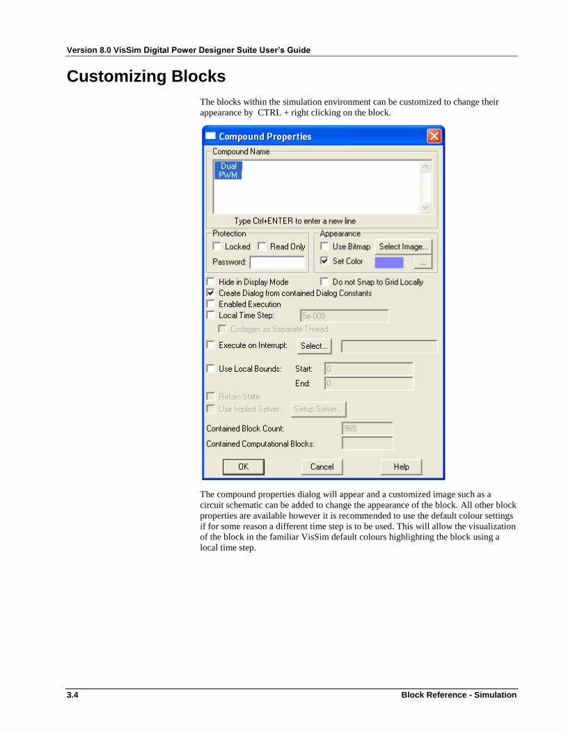
Version 8.0 VisSim Digital Power Designer Suite User’s Guide
3.4 Block Reference - Simulation
Customizing Blocks
The blocks within the simulation environment can be customized to change their
appearance by CTRL + right clicking on the block.
The compound properties dialog will appear and a customized image such as a
circuit schematic can be added to change the appearance of the block. All other block
properties are available however it is recommended to use the default colour settings
if for some reason a different time step is to be used. This will allow the visualization
of the block in the familiar VisSim default colours highlighting the block using a
local time step.

Version 8.0 VisSim Digital Power Designer Suite User’s Guide
Block Reference - Simulation 3.5
Sources
The sources in the digital power block set are ideal sources (zero output impedance)
with the possibility of summing together a large choice of options to create many
types of waveforms typically seen in digital power applications.
Although the sources are voltage sources as default and so described herein, they can
also be considered as ideal current or power sources, depending upon their use
within a simulation.
DC supply
Output Pins: Vdc DC supply output voltage (V)
Dialog properties:
The DC supply properties menu is shown in the following box which appears when
right-clicking on the block.
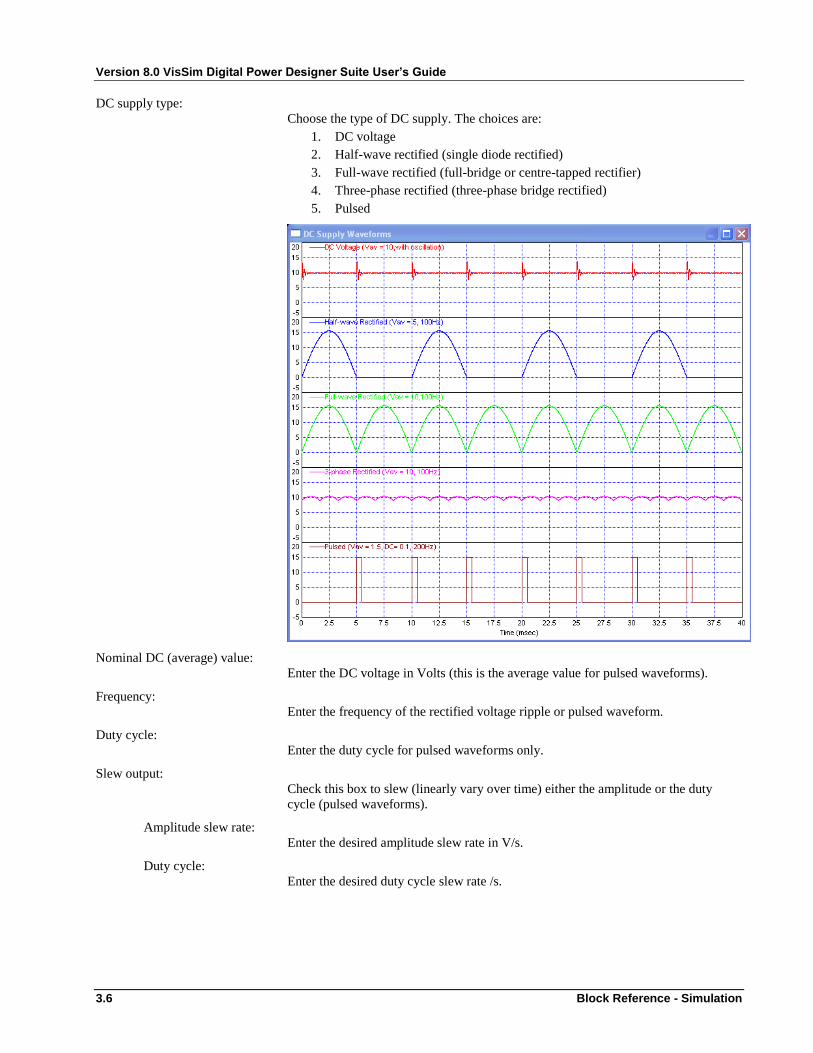
Version 8.0 VisSim Digital Power Designer Suite User’s Guide
3.6 Block Reference - Simulation
DC supply type:
Choose the type of DC supply. The choices are:
1. DC voltage
2. Half-wave rectified (single diode rectified)
3. Full-wave rectified (full-bridge or centre-tapped rectifier)
4. Three-phase rectified (three-phase bridge rectified)
5. Pulsed
Nominal DC (average) value:
Enter the DC voltage in Volts (this is the average value for pulsed waveforms).
Frequency:
Enter the frequency of the rectified voltage ripple or pulsed waveform.
Duty cycle:
Enter the duty cycle for pulsed waveforms only.
Slew output:
Check this box to slew (linearly vary over time) either the amplitude or the duty
cycle (pulsed waveforms).
Amplitude slew rate:
Enter the desired amplitude slew rate in V/s.
Duty cycle:
Enter the desired duty cycle slew rate /s.

Version 8.0 VisSim Digital Power Designer Suite User’s Guide
Block Reference - Simulation 3.7
Slew start time:
Enter the start time of the slewed parameter in seconds.
Slew stop time:
Enter the stop time of the slewed parameter in seconds.
Return to normal:
Check this box if the slewed parameters should return to the nominal setting.
Start transition time:
Enter the start time of the return slew to the nominal value.
Add amplitude step:
Check this box to add an instantaneous step to the output.
Step amplitude:
Enter the amplitude step required in percent of the DC voltage value.
Step start time:
Enter the start time of the amplitude step.
Step stop time:
Enter the end time of the amplitude step (returns to the nominal DC value).
Add impulse train:
Check this box to add impulses to the DC supply.
Time between impulses:
Enter the period of the impulses in milliseconds.
Impulse amplitude:
Enter the impulse amplitude in percent of the DC voltage.
Impulse duration:
Enter the duration of each impulse in milliseconds.
Alternate polarity:
Check this box if successive impulses are to alternate their polarity.
Impulse train start time:
Enter the start time of the impulse train.
Impulse train end time:
Enter the end time of the impulse train.
Add commutation ripple:
Check this box to include a triangular commutation ripple. This type a waveform can
be superimposed upon another waveform, for example, to construct a typical power
converter current waveform.
Ripple frequency:
Enter the frequency of the triangular ripple in kilohertz.
Duty cycle:
Enter the duty cycle of the triangular ripple.
Relative ripple amplitude:
Enter the amplitude of the triangular ripple relative to the amplitude of the DC
amplitude of the DC voltage.
Fixed amplitude:
Check this box to provide a fixed ripple amplitude independent upon the DC voltage.

Version 8.0 VisSim Digital Power Designer Suite User’s Guide
3.8 Block Reference - Simulation
Fixed ripple amplitude:
Enter the peak to peak amplitude in Volts.
Add damped oscillations:
Check this box to include repetitive damped oscillations. Damped oscillations would
be typically seen superimposed on a voltage waveform at the instance of the
switching of a power component.
Oscillation frequency:
Frequency of oscillation in kilohertz.
Time between impulses:
Repetition period of the oscillations in milliseconds..
Initial amplitude:
Initial amplitude (first peak) of the oscillations.
Damping factor:
The rate at which the oscillations will be damped.
Add noise:
A noise signal can be added to the source when this box is checked.
Noise amplitude:
Enter the relative amplitude of the noise in %.
Back

Version 8.0 VisSim Digital Power Designer Suite User’s Guide
Block Reference - Simulation 3.9
AC supply
Output Pins: Vac AC supply output voltage (V)
Dialog properties:
The AC supply properties menu is shown in the following box which appears when
right-clicking on the block.

Version 8.0 VisSim Digital Power Designer Suite User’s Guide
3.10 Block Reference - Simulation
Fundamental waveform:
Choose the AC supply type. The choices are:
1. Sinusoidal
2. square-wave
3. triangular
4. trapezoidal
5. three-level with ramp
Amplitude:
Enter the nominal amplitude of the AC waveform in Volts.
Phase:
Enter the desired phase (delay) of the AC waveform in degrees.
Offset:
Enter the required DC offset of the AC waveform in Volts.
Frequency:
Enter the desired nominal frequency of the AC waveform in Hertz.
Duty Cycle:
Enter the desired duty cycle ( not valid for sinusoidal waveforms).
Trapezoidal rise / fall time:
Enter the rise / fall time of the trapezoidal (0 = square wave).
3-level ramp height:
Enter the height of the ramp which will be added (placed on top) of the 3 level
square wave.

Version 8.0 VisSim Digital Power Designer Suite User’s Guide
Block Reference - Simulation 3.11
Maintain average value of square waves:
If checked, when varying the duty cycle of square waves, the average value of the
waveform will be maintained.
Slew amplitude/phase/frequency/duty cycle:
Check this box to enable slewing of any of the supply parameters.
Amplitude slew rate:
Enter the required amplitude slew rate in Volts / s.
Phase shift slew rate:
Enter the required phase difference slew rate in degrees / s.
Frequency slew rate:
Enter the required frequency slew rate in Hz / s.
Duty cycle slew rate:
Enter the required duty cycle slew rate (s-1
).
Slew start time:
Enter the start time of the parameter(s) slew.
Slew stop time:
Enter the end time of the parameter(s) slew.
Return to normal:
Check this box if it is desired that the slewed parameter(s) return to their nominal
values.
Start transition at time:
Enter the time at which the return slew should begin.
Add amplitude step:
Check this box to add an instantaneous step to the output.
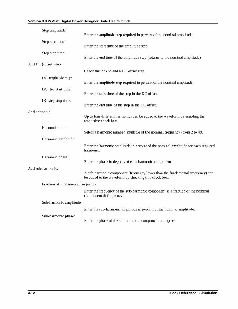
Version 8.0 VisSim Digital Power Designer Suite User’s Guide
3.12 Block Reference - Simulation
Step amplitude:
Enter the amplitude step required in percent of the nominal amplitude.
Step start time:
Enter the start time of the amplitude step.
Step stop time:
Enter the end time of the amplitude step (returns to the nominal amplitude).
Add DC (offset) step:
Check this box to add a DC offset step.
DC amplitude step:
Enter the amplitude step required in percent of the nominal amplitude.
DC step start time:
Enter the start time of the step in the DC offset.
DC step stop time:
Enter the end time of the step in the DC offset.
Add harmonic:
Up to four different harmonics can be added to the waveform by enabling the
respective check box.
Harmonic no.:
Select a harmonic number (multiple of the nominal frequency) from 2 to 49.
Harmonic amplitude:
Enter the harmonic amplitude in percent of the nominal amplitude for each required
harmonic.
Harmonic phase:
Enter the phase in degrees of each harmonic component.
Add sub-harmonic:
A sub-harmonic component (frequency lower than the fundamental frequency) can
be added to the waveform by checking this check box.
Fraction of fundamental frequency:
Enter the frequency of the sub-harmonic component as a fraction of the nominal
(fundamental) frequency.
Sub-harmonic amplitude:
Enter the sub-harmonic amplitude in percent of the nominal amplitude.
Sub-harmonic phase:
Enter the phase of the sub-harmonic component in degrees.
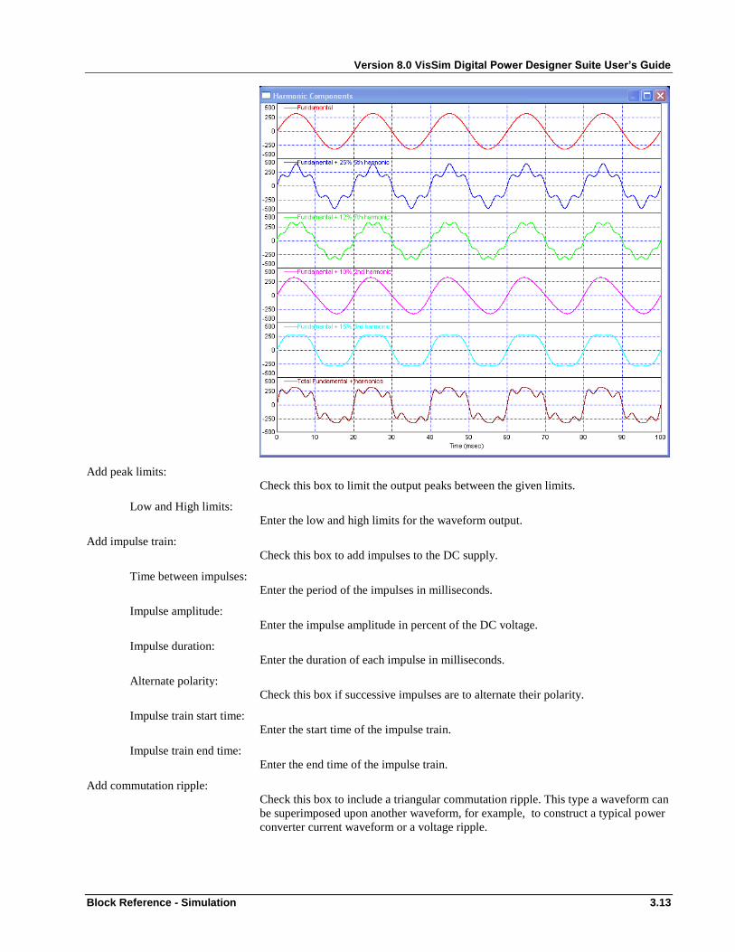
Version 8.0 VisSim Digital Power Designer Suite User’s Guide
Block Reference - Simulation 3.13
Add peak limits:
Check this box to limit the output peaks between the given limits.
Low and High limits:
Enter the low and high limits for the waveform output.
Add impulse train:
Check this box to add impulses to the DC supply.
Time between impulses:
Enter the period of the impulses in milliseconds.
Impulse amplitude:
Enter the impulse amplitude in percent of the DC voltage.
Impulse duration:
Enter the duration of each impulse in milliseconds.
Alternate polarity:
Check this box if successive impulses are to alternate their polarity.
Impulse train start time:
Enter the start time of the impulse train.
Impulse train end time:
Enter the end time of the impulse train.
Add commutation ripple:
Check this box to include a triangular commutation ripple. This type a waveform can
be superimposed upon another waveform, for example, to construct a typical power
converter current waveform or a voltage ripple.

Version 8.0 VisSim Digital Power Designer Suite User’s Guide
3.14 Block Reference - Simulation
Ripple frequency:
Enter the frequency of the triangular ripple in kilohertz.
Duty cycle:
Enter the duty cycle of the triangular ripple.
Relative ripple amplitude:
Enter the amplitude of the triangular ripple relative to the amplitude of the DC
amplitude of the DC voltage.
Fixed ripple amplitude:
Check this box to provide a fixed ripple amplitude independent upon the DC voltage.
Fixed ripple amplitude:
Enter the peak to peak amplitude in Volts.
Add damped oscillations:
Check this box to include repetitive damped oscillations. Damped oscillations would
be typically seen superimposed on a voltage waveform at the instance of the
switching of a power component.
Oscillation frequency:
Frequency of oscillation in kilohertz.
Time between impulses:
Repetition period of the oscillations in milliseconds..
Initial amplitude:
Initial amplitude (first peak) of the oscillations.
Damping factor:
The rate at which the oscillations will be damped.
Add noise:
A noise signal can be added to the source when this box is checked.
Noise amplitude:
Enter the relative amplitude of the noise in %.
Remove fundamental component from output:
Check this box if the fundamental component is to be removed from the AC supply
output (only the individual harmonic components and / or other components remain).
Three-phase AC supply
Output Pins: V(L1, L2, L3) Three-phase AC supply output voltage (V), vector (rows = 1, columns = 3)
N Effective Neutral Voltage (V) (with respect to a zero point of the three phases).
Dialog properties:
The three-phase AC supply properties menu is shown in the following box which
appears when right-clicking on the block.
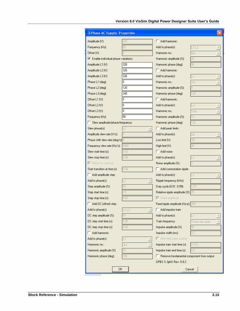
Version 8.0 VisSim Digital Power Designer Suite User’s Guide
Block Reference - Simulation 3.15

Version 8.0 VisSim Digital Power Designer Suite User’s Guide
3.16 Block Reference - Simulation
Amplitude:
Enter the nominal default amplitude of the AC waveform in Volts.
Frequency:
Enter the nominal default frequency of the AC waveform in Hertz.
Offset:
Enter the default DC offset of the AC waveform in Volts.
In the default case here, the phase lag of the three phases will be 0°, 120° and 240°.
Enable individual phase variations:
Check this box to enable all the possible variations of the three-phase AC supply,
otherwise the default values are used.
Amplitude L1, L2 and L3:
Enter the nominal amplitude individually for the three phases of the AC waveforms
in Volts.
Phase L1, L2 and L3:
Enter the nominal phase difference individually for the three phases of the AC
waveform in degrees.
Offset L1, L2 and L3:
Enter the default DC offset of the three phases individually.
Frequency:
Enter the variable nominal frequency of the three-phase AC waveforms in Hertz.
Slew amplitude/phase/frequency:
Check this box to enable slewing of any of the supply parameters.
Slew phase(s):
Select the phase or phases to be slewed at the set rate.
Amplitude slew rate:
Enter the required amplitude slew rate in Volts / s.
Phase shift slew rate:
Enter the required phase difference slew rate in degrees / s.
Frequency slew rate:
Enter the required frequency slew rate in Hz / s.
Slew start time:
Enter the start time of the parameter(s) slew.
Slew stop time:
Enter the end time of the parameter(s) slew.
Return to normal:
Check this box if it is desired that the slewed parameter(s) return to their nominal
values.
Start transition at time:
Enter the time at which the return slew should begin.
Add amplitude step:
Check this box to add an instantaneous step to the output.

Version 8.0 VisSim Digital Power Designer Suite User’s Guide
Block Reference - Simulation 3.17
Add to phase(s):
Select the phase or phases to add the amplitude step.
Step amplitude:
Enter the amplitude step required in percent of the nominal amplitude.
Step start time:
Enter the start time of the amplitude step.
Step stop time:
Enter the end time of the amplitude step (returns to the nominal amplitude).
Add DC (offset) step:
Check this box to add a DC offset step.
Add to phase(s):
Select the phase or phases to add the offset step.
DC amplitude step:
Enter the amplitude step required in percent of the nominal amplitude.
DC step start time:
Enter the start time of the step in the DC offset.
DC step stop time:
Enter the end time of the step in the DC offset.
Add harmonic:
Up to four different harmonics can be added to the waveform by enabling the
respective check box.
Add to phase(s):
Select the phase or phases to add the harmonic component.
Harmonic no.:
Select a harmonic number (multiple of the nominal frequency) from 2 to 49.
Harmonic amplitude:
Enter the harmonic amplitude in percent of the nominal amplitude for each required
harmonic.
Harmonic phase:
Enter the phase in degrees of each harmonic component.
Add peak limits:
Check this box to limit the output peaks between the given limits.
Add to phase(s):
Select the phase or phases to include peak limits.
Low and High limits:
Enter the high and low limits for the selected output phases.
Add noise:
A noise signal can be added to the source when this box is checked.
Add to phase(s):
Select the phase or phases to add the noise component.
Noise amplitude:
Enter the relative amplitude of the noise in %.
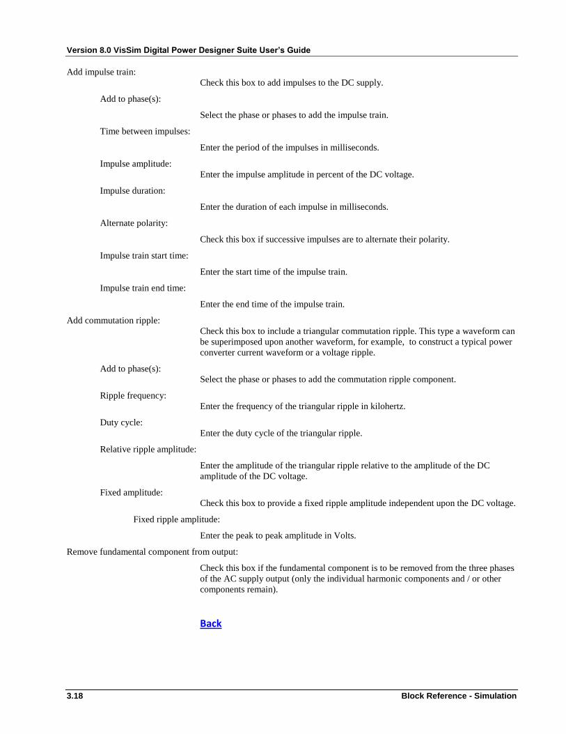
Version 8.0 VisSim Digital Power Designer Suite User’s Guide
3.18 Block Reference - Simulation
Add impulse train:
Check this box to add impulses to the DC supply.
Add to phase(s):
Select the phase or phases to add the impulse train.
Time between impulses:
Enter the period of the impulses in milliseconds.
Impulse amplitude:
Enter the impulse amplitude in percent of the DC voltage.
Impulse duration:
Enter the duration of each impulse in milliseconds.
Alternate polarity:
Check this box if successive impulses are to alternate their polarity.
Impulse train start time:
Enter the start time of the impulse train.
Impulse train end time:
Enter the end time of the impulse train.
Add commutation ripple:
Check this box to include a triangular commutation ripple. This type a waveform can
be superimposed upon another waveform, for example, to construct a typical power
converter current waveform or a voltage ripple.
Add to phase(s):
Select the phase or phases to add the commutation ripple component.
Ripple frequency:
Enter the frequency of the triangular ripple in kilohertz.
Duty cycle:
Enter the duty cycle of the triangular ripple.
Relative ripple amplitude:
Enter the amplitude of the triangular ripple relative to the amplitude of the DC
amplitude of the DC voltage.
Fixed amplitude:
Check this box to provide a fixed ripple amplitude independent upon the DC voltage.
Fixed ripple amplitude:
Enter the peak to peak amplitude in Volts.
Remove fundamental component from output:
Check this box if the fundamental component is to be removed from the three phases
of the AC supply output (only the individual harmonic components and / or other
components remain).
Back

Version 8.0 VisSim Digital Power Designer Suite User’s Guide
Block Reference - Simulation 3.19
Controlled AC supply
Input Pins: Amp Set the amplitude of the AC supply using this pin.
OS Set the DC offset of the AC supply output using this pin.
PH Set the phase of the AC supply output using this pin.
F Set the frequency of the AC supply output using this pin.
DC Set the duty cycle of the AC supply (non-sinusoidal) output using this pin.
Tz r/f Set the rise/fall time of the trapezoidal AC supply output using this pin.
3L Set the amplitude of the ramp of the 3-level AC supply output using this pin.
Output Pins: Vac AC supply output voltage (V).
Dialog properties:
The controlled AC supply properties menu is shown in the following box which
appears when right-clicking on the block.
This block is similar to the AC supply block except that the parameters can be varied
using the input pins.
Fundamental waveform:
Choose the AC supply type. The choices are:
1. Sinusoidal
2. square-wave
3. triangular
4. trapezoidal
5. three-level with ramp
Controlled-slew AC supply
Input Pins: dV Control the rate of change of amplitude of the AC supply using this pin.
dOS Control the rate of change offset of the AC supply output using this pin.

Version 8.0 VisSim Digital Power Designer Suite User’s Guide
3.20 Block Reference - Simulation
dPH Control the rate of change of phase of the AC supply output using this pin.
dF Control the rate of change frequency of the AC supply output using this pin.
dDC Control the rate of change of duty cycle of the AC supply (non-sinusoidal) output
using this pin.
Output Pins: Vac AC supply output voltage (V).
Dialog properties:
The controlled-slew AC supply properties menu is shown in the following box which
appears when right-clicking on the block
The base values of the supply are set in the dialog similar to the AC supply block.
The value at the input pins will vary these base values at the rate of the input value.
Controlled-slew DC supply
Input Pins: dV Control rate of change of amplitude of the DC supply using this pin.
dDC Control the rate of change of duty cycle of the DC supply (only pulsed supply)
output using this pin.
Output Pins: Vdc DC output voltage.
Dialog properties:
The controlled-slew DC supply properties menu is shown in the following box which
appears when right-clicking on the block
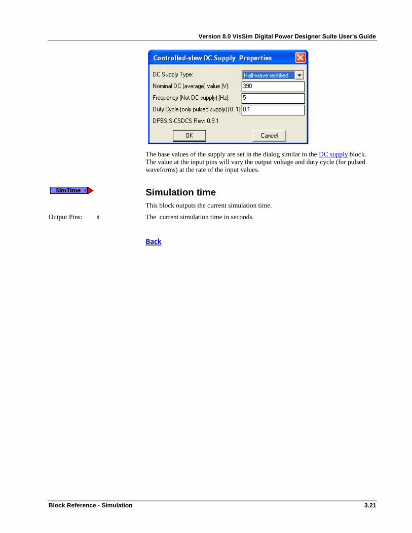
Version 8.0 VisSim Digital Power Designer Suite User’s Guide
Block Reference - Simulation 3.21
The base values of the supply are set in the dialog similar to the DC supply block.
The value at the input pins will vary the output voltage and duty cycle (for pulsed
waveforms) at the rate of the input values.
Simulation time
This block outputs the current simulation time.
Output Pins: t The current simulation time in seconds.
Back

Version 8.0 VisSim Digital Power Designer Suite User’s Guide
3.22 Block Reference - Simulation
Sensors
The sensors sub-section within the simulation section of the digital power block set
are designed to emulate many typical voltage and current sensors used in digital
power applications.
Resistive divider (voltage sense)
Input Pins: Vin Sensed input voltage (V).
Output Pins: Vo Sensor output voltage (V)
Circuit schematic:
Dialog properties:
The resistive divider block properties menu is shown in the following box which
appears when right-clicking on the block.
Series resistor value R1:
Enter the value of the series resistor R1 in Ohms.
Parallel resistor R2:
Enter the value of the parallel resistor R2 in Ohms.
Add capacitor in parallel with R2:
Enables a single pole in the voltage measurement (for filtering noise or anti-aliasing).
Capacitance C1:
Enter the value of the capacitor C1 in nano-Farads.
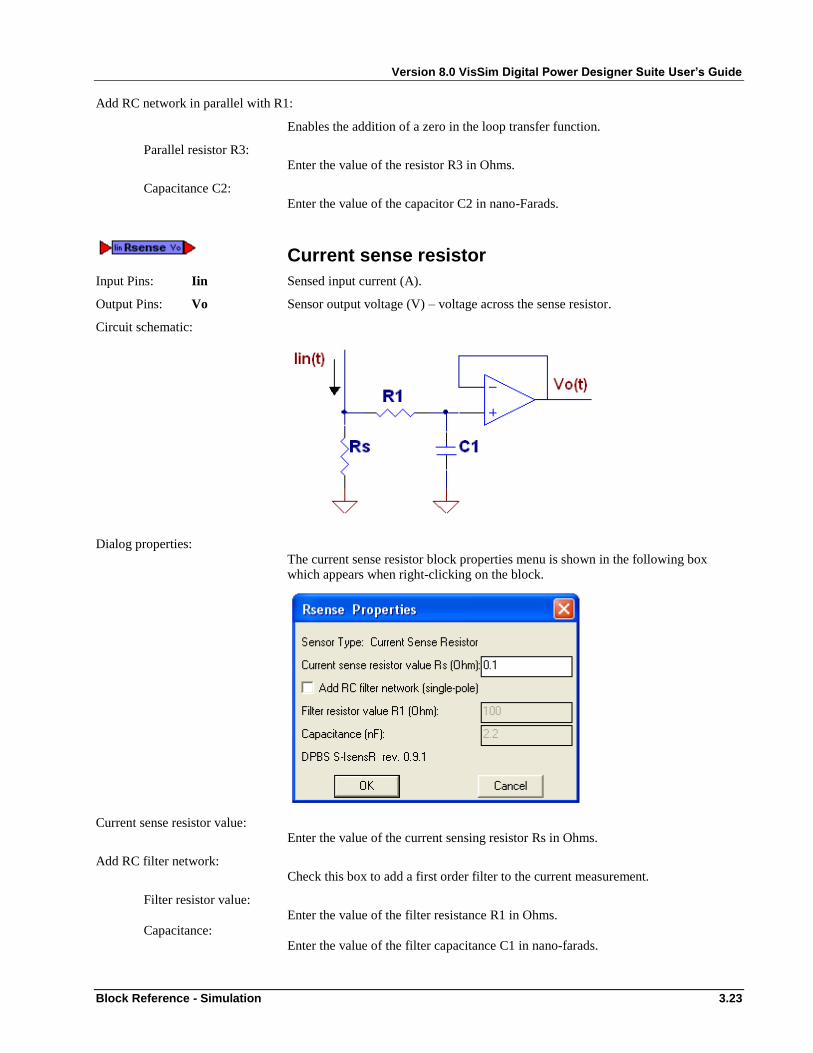
Version 8.0 VisSim Digital Power Designer Suite User’s Guide
Block Reference - Simulation 3.23
Add RC network in parallel with R1:
Enables the addition of a zero in the loop transfer function.
Parallel resistor R3:
Enter the value of the resistor R3 in Ohms.
Capacitance C2:
Enter the value of the capacitor C2 in nano-Farads.
Current sense resistor
Input Pins: Iin Sensed input current (A).
Output Pins: Vo Sensor output voltage (V) – voltage across the sense resistor.
Circuit schematic:
Dialog properties:
The current sense resistor block properties menu is shown in the following box
which appears when right-clicking on the block.
Current sense resistor value:
Enter the value of the current sensing resistor Rs in Ohms.
Add RC filter network:
Check this box to add a first order filter to the current measurement.
Filter resistor value:
Enter the value of the filter resistance R1 in Ohms.
Capacitance:
Enter the value of the filter capacitance C1 in nano-farads.

Version 8.0 VisSim Digital Power Designer Suite User’s Guide
3.24 Block Reference - Simulation
AC current transformer
Input Pins: Iin Sensed primary current (A).
Output Pins: Vo Sensor output voltage (V) – voltage across the burden resistor.
Dialog properties:
The AC current transformer block properties menu is shown in the following box
which appears when right-clicking on the block.
Current ration Ip / Is:
Enter the current transformer primary to secondary current transfer ratio (A/A).
Maximum primary peak saturation current:
The saturation current referred to the primary winding – the secondary sense current
will be limited at this value times the current ratio.
Maximum power rating:
The power rating of the current transformer – the average output power will be
limited at this value.
Secondary magnetizing inductance:
The magnetizing inductance of the secondary winding in milli-Henries.
Inter-winding capacitance
The capacitance of the windings which together with the magnetizing inductance
determines the frequency response of the current sensing transformer.
Insert directly the frequency response parameters:
If the current transformer parameters are not known, the frequency response
parameters can be directly entered if this box is checked.
Centre frequency:
Enter the centre band frequency in kilohertz.
Quality factor:
Enter the quality factor, Q, of the current transformer response.
Burden resistor value:
Enter the value of the burden resistance (current transformer load) in Ohms.
Include secondary rectifier diode:
A diode can be included on the current transformer secondary to maintain positive
values only (in practise, a current path will be required for the negative current in

Version 8.0 VisSim Digital Power Designer Suite User’s Guide
Block Reference - Simulation 3.25
order to reset the winding and it is assumed that this has been correctly performed so
that this effect is not accounted for here).
Diode forward voltage drop:
Enter the forward voltage drop of the rectifier diode in Volts.
Add output voltage offset:
Check this box to add a DC offset to the measurement (e.g. for measuring AC
currents with a positive supply only).
Offset voltage:
Enter the offset voltage in Volts.
Include RC filter network:
Check this to include a first order filter on the voltage output.
Filter resistor value:
Enter the filter resistance value in Ohms.
Capacitance:
Enter the filter capacitance value in nano-farads.
Back
Isolated current sensor
This sensor is designed to model a hall type of current sensor which is capable of
measuring both DC and AC currents.
Input Pins: Iin Sensed input current (A).
Output Pins: Vo Sensor output voltage (V).
Dialog properties:
The isolated current sensor block properties menu is shown in the following box
which appears when right-clicking on the block.
3dB cut-off frequency:
The cut-off frequency of the sensor or the bandwidth.

Version 8.0 VisSim Digital Power Designer Suite User’s Guide
3.26 Block Reference - Simulation
Reaction time to 10%:
This is the time it takes for the output to reach 10% of its final output on an input
step and can be found in the datasheet of a particular device.
Gain:
This is the gain of the device in millivolts / amperes for a voltage output device.
Output high-level saturation voltage:
The maximum high-level output voltage for a voltage output device.
Output low-level saturation voltage:
T he minimum low-level output voltage for a voltage output device.
Current output:
Current sensors can have either a voltage or a current output. For hall sensors,
generally an open-loop device has a voltage output while a closed-loop, compensated
device has a current output. Check this box for a current output device.
Gain:
This is the gain for a current output device in milli-amperes / amperes.
Output saturation current:
The output secondary saturation current in Amperes. It is assumed that the device is
bi-polar in this case and the current saturation is dual polarity.
Load resistance:
The load resistance on the current output sensor in Ohms.
Bi-polar output:
Check this box for a bi-polar measurement (both sensors have a voltage output at this
point since the current sensor has a load resistance converting it to voltage).
Ground (zero) voltage level:
Enter the ground voltage level required (this option can apply an offset to a bi-polar
sensor centered at the ground or zero voltage in order to measure both positive and
negative currents with a uni-polar ADC).
Add RC filter network:
A single pole RC filter can be added at the output of the sensor.
Filter resistor:
Enter the filter resistance value in Ohms.
Capacitance:
Enter the filter capacitance value in nano-farads.
Isolated voltage sensor
This sensor is designed to model an isolated voltage sensor and can be either an
opto-isolated type of sensor with amplifier or a hall type of voltage sensor. The
sensor is capable of measuring both DC and AC voltages.
Input Pins: Vin Sensed input voltage (A).
Output Pins: Vo Sensor output voltage (V).
Dialog properties:
The isolated voltage sensor block properties menu is shown in the following box
which appears when right-clicking on the block.
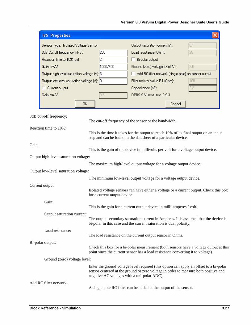
Version 8.0 VisSim Digital Power Designer Suite User’s Guide
Block Reference - Simulation 3.27
3dB cut-off frequency:
The cut-off frequency of the sensor or the bandwidth.
Reaction time to 10%:
This is the time it takes for the output to reach 10% of its final output on an input
step and can be found in the datasheet of a particular device.
Gain:
This is the gain of the device in millivolts per volt for a voltage output device.
Output high-level saturation voltage:
The maximum high-level output voltage for a voltage output device.
Output low-level saturation voltage:
T he minimum low-level output voltage for a voltage output device.
Current output:
Isolated voltage sensors can have either a voltage or a current output. Check this box
for a current output device.
Gain:
This is the gain for a current output device in milli-amperes / volt.
Output saturation current:
The output secondary saturation current in Amperes. It is assumed that the device is
bi-polar in this case and the current saturation is dual polarity.
Load resistance:
The load resistance on the current output sensor in Ohms.
Bi-polar output:
Check this box for a bi-polar measurement (both sensors have a voltage output at this
point since the current sensor has a load resistance converting it to voltage).
Ground (zero) voltage level:
Enter the ground voltage level required (this option can apply an offset to a bi-polar
sensor centered at the ground or zero voltage in order to measure both positive and
negative AC voltages with a uni-polar ADC).
Add RC filter network:
A single pole RC filter can be added at the output of the sensor.

Version 8.0 VisSim Digital Power Designer Suite User’s Guide
3.28 Block Reference - Simulation
Filter resistor:
Enter the filter resistance value in Ohms.
Capacitance:
Enter the filter capacitance value in nano-farads.
Back
Operational amplifier
This block models a typical operational amplifier (op-amp) circuit including the
input and feedback resistances to determine the closed-loop gain and optionally a
capacitance to modify the closed-loop pole frequency.
Input Pins: Vin Input voltage (V).
Output Pins: Vo Output voltage (V).
Dialog properties:
The op-amp block properties menu is shown in the following box which appears
when right-clicking on the block.
Circuit configuration:
The choices here are:
1. Inverting amplifier
2. Non-inverting amplifier
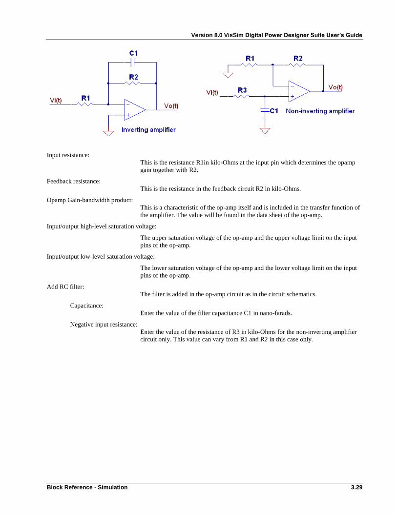
Version 8.0 VisSim Digital Power Designer Suite User’s Guide
Block Reference - Simulation 3.29
Input resistance:
This is the resistance R1in kilo-Ohms at the input pin which determines the opamp
gain together with R2.
Feedback resistance:
This is the resistance in the feedback circuit R2 in kilo-Ohms.
Opamp Gain-bandwidth product:
This is a characteristic of the op-amp itself and is included in the transfer function of
the amplifier. The value will be found in the data sheet of the op-amp.
Input/output high-level saturation voltage:
The upper saturation voltage of the op-amp and the upper voltage limit on the input
pins of the op-amp.
Input/output low-level saturation voltage:
The lower saturation voltage of the op-amp and the lower voltage limit on the input
pins of the op-amp.
Add RC filter:
The filter is added in the op-amp circuit as in the circuit schematics.
Capacitance:
Enter the value of the filter capacitance C1 in nano-farads.
Negative input resistance:
Enter the value of the resistance of R3 in kilo-Ohms for the non-inverting amplifier
circuit only. This value can vary from R1 and R2 in this case only.
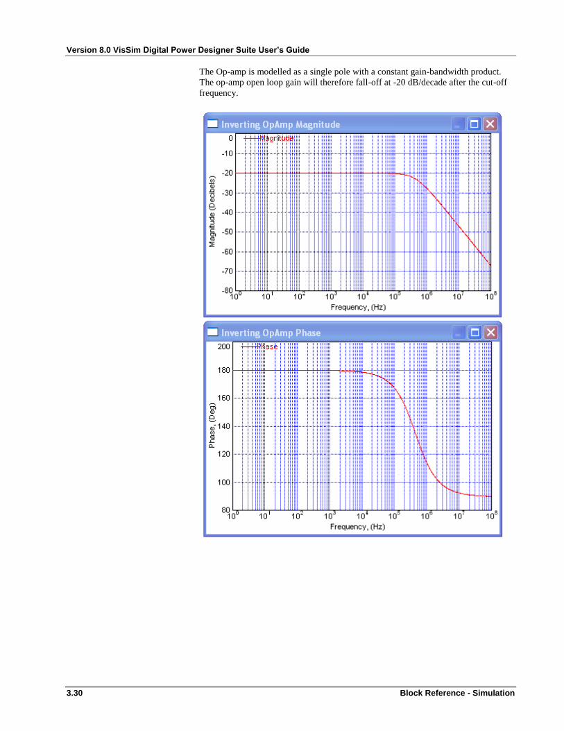
Version 8.0 VisSim Digital Power Designer Suite User’s Guide
3.30 Block Reference - Simulation
The Op-amp is modelled as a single pole with a constant gain-bandwidth product.
The op-amp open loop gain will therefore fall-off at -20 dB/decade after the cut-off
frequency.
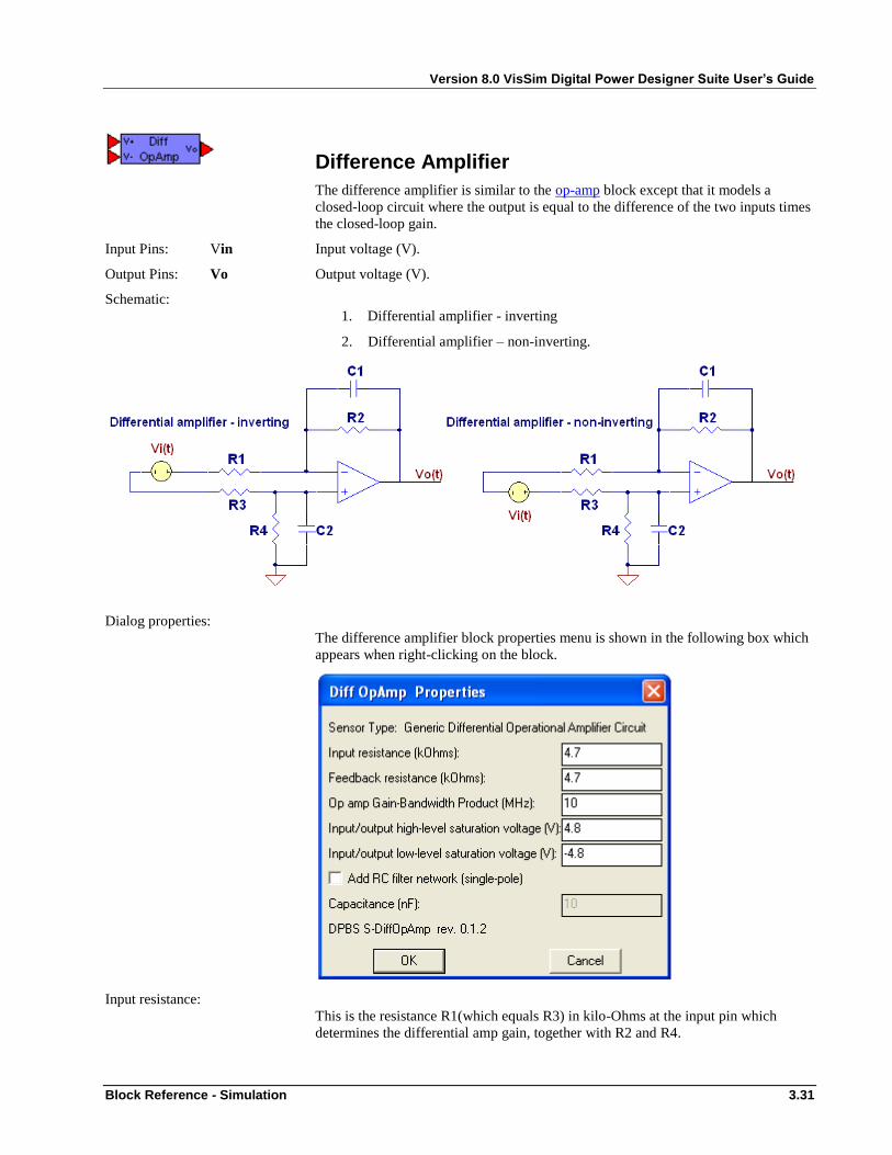
Version 8.0 VisSim Digital Power Designer Suite User’s Guide
Block Reference - Simulation 3.31
Difference Amplifier
The difference amplifier is similar to the op-amp block except that it models a
closed-loop circuit where the output is equal to the difference of the two inputs times
the closed-loop gain.
Input Pins: Vin Input voltage (V).
Output Pins: Vo Output voltage (V).
Schematic:
1. Differential amplifier - inverting
2. Differential amplifier – non-inverting.
Dialog properties:
The difference amplifier block properties menu is shown in the following box which
appears when right-clicking on the block.
Input resistance:
This is the resistance R1(which equals R3) in kilo-Ohms at the input pin which
determines the differential amp gain, together with R2 and R4.

Version 8.0 VisSim Digital Power Designer Suite User’s Guide
3.32 Block Reference - Simulation
Feedback resistance:
This is the resistance in the feedback circuit R2 (which equals R4) in kilo-Ohms.
Opamp Gain-bandwidth product:
This is a characteristic of the op-amp itself and is included in the transfer function of
the amplifier. The value will be found in the data sheet of the op-amp.
Input/output high-level saturation voltage:
The upper saturation voltage of the op-amp and the upper voltage limit on the input
pins of the op-amp.
Input/output low-level saturation voltage:
The lower saturation voltage of the op-amp and the lower voltage limit on the input
pins of the op-amp.
Note that, for simplicity, it is assumed that the op-amp input and output limits are
identical and that the op-amp differential input voltage limit is twice that of each
input limit. If different limiting values are needed to be applied for the input and
output, they can be applied externally to the block. Note also that the input limit
refers to the limit at the input pins at the op-amp itself and not the limit of the op-
amp input circuit or the block input. High input voltages can be used at the input if
large values of input resistance (with respect to the feedback resistance) are used.
Add RC filter:
The filter is added in the differential amp circuit as in the circuit schematics.
Capacitance:
Enter the value of the filter capacitance C1 (which equals C2) in nano-farads.
The difference amplifier is modelled similarly to the op-amp block with differences
due only to the external circuit configuration.
Back
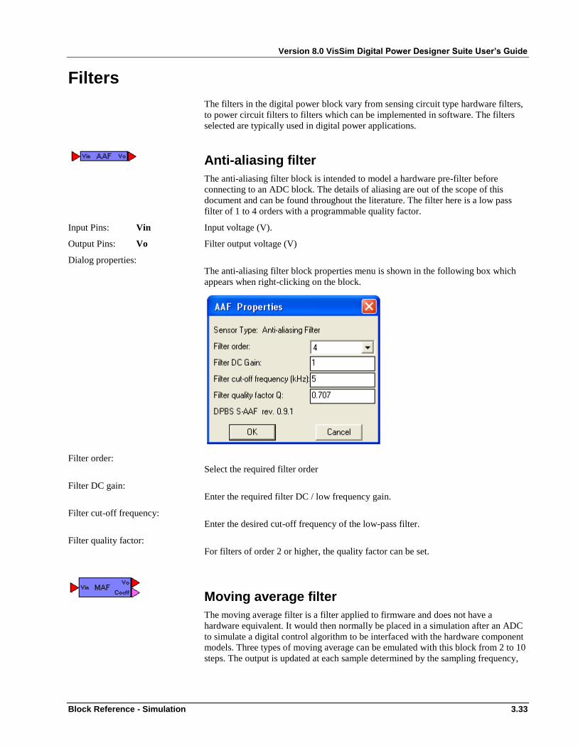
Version 8.0 VisSim Digital Power Designer Suite User’s Guide
Block Reference - Simulation 3.33
Filters
The filters in the digital power block vary from sensing circuit type hardware filters,
to power circuit filters to filters which can be implemented in software. The filters
selected are typically used in digital power applications.
Anti-aliasing filter
The anti-aliasing filter block is intended to model a hardware pre-filter before
connecting to an ADC block. The details of aliasing are out of the scope of this
document and can be found throughout the literature. The filter here is a low pass
filter of 1 to 4 orders with a programmable quality factor.
Input Pins: Vin Input voltage (V).
Output Pins: Vo Filter output voltage (V)
Dialog properties:
The anti-aliasing filter block properties menu is shown in the following box which
appears when right-clicking on the block.
Filter order:
Select the required filter order
Filter DC gain:
Enter the required filter DC / low frequency gain.
Filter cut-off frequency:
Enter the desired cut-off frequency of the low-pass filter.
Filter quality factor:
For filters of order 2 or higher, the quality factor can be set.
Moving average filter
The moving average filter is a filter applied to firmware and does not have a
hardware equivalent. It would then normally be placed in a simulation after an ADC
to simulate a digital control algorithm to be interfaced with the hardware component
models. Three types of moving average can be emulated with this block from 2 to 10
steps. The output is updated at each sample determined by the sampling frequency,

Version 8.0 VisSim Digital Power Designer Suite User’s Guide
3.34 Block Reference - Simulation
each sample being pushed through the filter similar to a FIFO; the newest sample
having the highest weighting and the oldest sample being pushed out of the window.
Input Pins: Vin Input voltage (V).
Output Pins: Vo Filter output voltage (V)
Coeff Display of the filter coefficients (struct).
Dialog properties:
The moving average filter block properties menu is shown in the following box
which appears when right-clicking on the block.
Moving average type:
The choices here are:
1. simple (each step has equal weighting)
2. linearly weighted (each past time step has an equal, decreasing difference in
weighting)
3. exponential (each past time step is weighted in an exponentially decreasing rate)
Number of steps:
From 2 to 10 steps may be selected.
Exponential weighting factor:
Enter a value from 0.1 to 0.99 which will correspond to the weighting of the most
recent step (sample); the remaining coefficients will be correspondingly
exponentially weighted. This value is only relevant if an exponentially weighted
filter is selected.
DC gain:
A gain coefficient will be determined in order to set the required DC filter gain.
Sampling frequency:
Enter the required sampling frequency in kHz. The coefficients are not dependent
upon the sampling frequency.
Output high / low limit:
Enter the output high and low limits of the filter.
Back
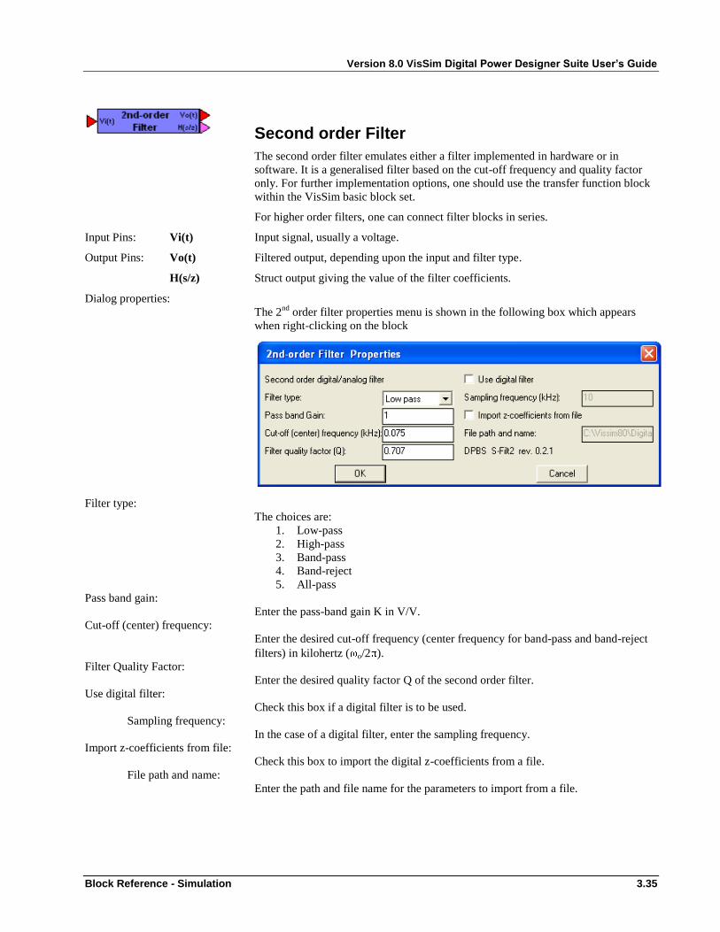
Version 8.0 VisSim Digital Power Designer Suite User’s Guide
Block Reference - Simulation 3.35
Second order Filter
The second order filter emulates either a filter implemented in hardware or in
software. It is a generalised filter based on the cut-off frequency and quality factor
only. For further implementation options, one should use the transfer function block
within the VisSim basic block set.
For higher order filters, one can connect filter blocks in series.
Input Pins: Vi(t) Input signal, usually a voltage.
Output Pins: Vo(t) Filtered output, depending upon the input and filter type.
H(s/z) Struct output giving the value of the filter coefficients.
Dialog properties:
The 2nd
order filter properties menu is shown in the following box which appears
when right-clicking on the block
Filter type:
The choices are:
1. Low-pass
2. High-pass
3. Band-pass
4. Band-reject
5. All-pass
Pass band gain:
Enter the pass-band gain K in V/V.
Cut-off (center) frequency:
Enter the desired cut-off frequency (center frequency for band-pass and band-reject
filters) in kilohertz ( o/2 ).
Filter Quality Factor:
Enter the desired quality factor Q of the second order filter.
Use digital filter:
Check this box if a digital filter is to be used.
Sampling frequency:
In the case of a digital filter, enter the sampling frequency.
Import z-coefficients from file:
Check this box to import the digital z-coefficients from a file.
File path and name:
Enter the path and file name for the parameters to import from a file.
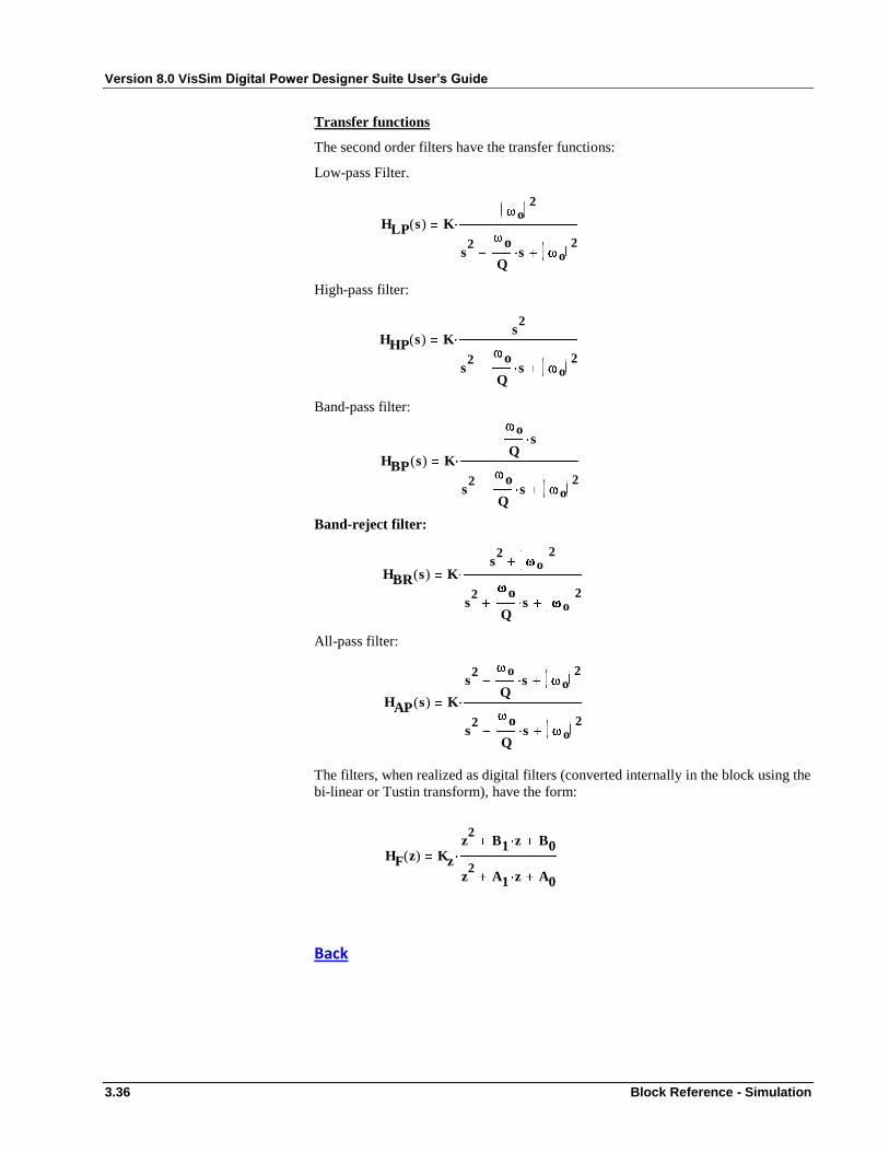
Version 8.0 VisSim Digital Power Designer Suite User’s Guide
3.36 Block Reference - Simulation
Transfer functions
The second order filters have the transfer functions:
Low-pass Filter.
High-pass filter:
Band-pass filter:
Band-reject filter:
All-pass filter:
The filters, when realized as digital filters (converted internally in the block using the
bi-linear or Tustin transform), have the form:
Back
HLP s( ) Ko
2
s2 o
Qs o
2
HHP s( ) Ks2
s2 o
Qs o
2
HBP s( ) K
o
Qs
s2 o
Qs o
2
HBR s( ) Ks2
o2
s2 o
Qs o
2
HAP s( ) K
s2 o
Qs o
2
s2 o
Qs o
2
HF z( ) Kz
z2
B1 z B0
z2
A1 z A0

Version 8.0 VisSim Digital Power Designer Suite User’s Guide
Block Reference - Simulation 3.37
RC Filter
The RC filter emulates a first order hardware filter using a single resistor and a single
capacitor. This filter is intended for use as a sense filter on any sensing circuits but
can be applied as a general first order filter.
Input pin: Vi Unfiltered input voltage (V).
Output Pin: Vo Filtered output voltage (V).
Dialog properties:
The RC filter properties menu is shown in the following box which appears when
right-clicking on the block
Filter type:
The choices are:
1. Low-pass
2. High-pass
Resistance:
Enter the series (low-pass) or parallel (high-pass) resistance value in Ohms.
Capacitance:
Enter the filter capacitance value in nano-Farads.
Back

Version 8.0 VisSim Digital Power Designer Suite User’s Guide
3.38 Block Reference - Simulation
Power LC Filter
The power LC filter is a second order hardware filter using an inductor and a
capacitor. This filter is intended for use in the power stage of circuits and not as a
sensing filter. The filter can be applied as a converter input or output filter. If
damping is required, the internal inductor and / or capacitor resistances can be
increased to emulate series resistances. The filter can be applied with DC or AC
voltages.
Input Pins: Vin Unfiltered input voltage (V).
%Load/Io Input which can be selected as a percentage load input or as the filter load current
input.
Output pins: Vo Filtered output voltage (V).
Io Filtered output current (A).
Iin Unfiltered input current (A).
vL The voltage across the filter inductor (V).
iC The current in the filter capacitance (A).
Circuit schematic: Power LC filter.
Dialog properties:
The power LC filter properties menu is shown in the following box which appears
when right-clicking on the block
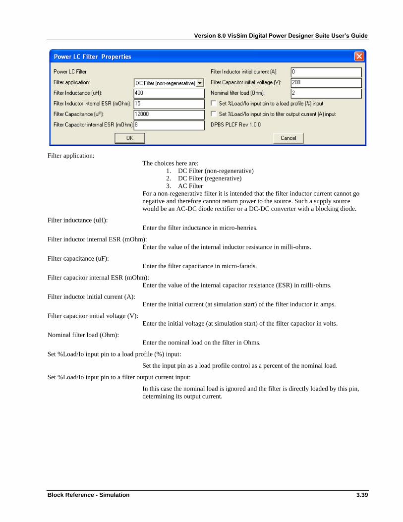
Version 8.0 VisSim Digital Power Designer Suite User’s Guide
Block Reference - Simulation 3.39
Filter application:
The choices here are:
1. DC Filter (non-regenerative)
2. DC Filter (regenerative)
3. AC Filter
For a non-regenerative filter it is intended that the filter inductor current cannot go
negative and therefore cannot return power to the source. Such a supply source
would be an AC-DC diode rectifier or a DC-DC converter with a blocking diode.
Filter inductance (uH):
Enter the filter inductance in micro-henries.
Filter inductor internal ESR (mOhm):
Enter the value of the internal inductor resistance in milli-ohms.
Filter capacitance (uF):
Enter the filter capacitance in micro-farads.
Filter capacitor internal ESR (mOhm):
Enter the value of the internal capacitor resistance (ESR) in milli-ohms.
Filter inductor initial current (A):
Enter the initial current (at simulation start) of the filter inductor in amps.
Filter capacitor initial voltage (V):
Enter the initial voltage (at simulation start) of the filter capacitor in volts.
Nominal filter load (Ohm):
Enter the nominal load on the filter in Ohms.
Set %Load/Io input pin to a load profile (%) input:
Set the input pin as a load profile control as a percent of the nominal load.
Set %Load/Io input pin to a filter output current input:
In this case the nominal load is ignored and the filter is directly loaded by this pin,
determining its output current.
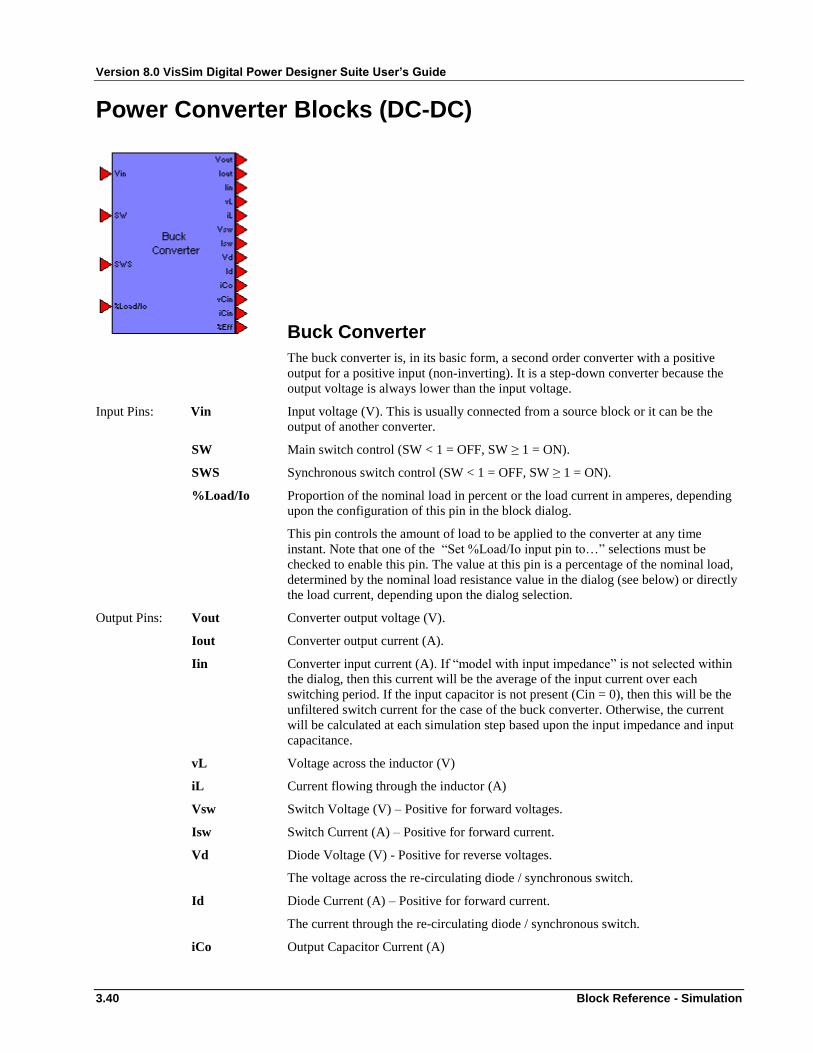
Version 8.0 VisSim Digital Power Designer Suite User’s Guide
3.40 Block Reference - Simulation
Power Converter Blocks (DC-DC)
Buck Converter
The buck converter is, in its basic form, a second order converter with a positive
output for a positive input (non-inverting). It is a step-down converter because the
output voltage is always lower than the input voltage.
Input Pins: Vin Input voltage (V). This is usually connected from a source block or it can be the
output of another converter.
SW Main switch control (SW < 1 = OFF, SW ≥ 1 = ON).
SWS Synchronous switch control (SW < 1 = OFF, SW ≥ 1 = ON).
%Load/Io Proportion of the nominal load in percent or the load current in amperes, depending
upon the configuration of this pin in the block dialog.
This pin controls the amount of load to be applied to the converter at any time
instant. Note that one of the “Set %Load/Io input pin to…” selections must be
checked to enable this pin. The value at this pin is a percentage of the nominal load,
determined by the nominal load resistance value in the dialog (see below) or directly
the load current, depending upon the dialog selection.
Output Pins: Vout Converter output voltage (V).
Iout Converter output current (A).
Iin Converter input current (A). If “model with input impedance” is not selected within
the dialog, then this current will be the average of the input current over each
switching period. If the input capacitor is not present (Cin = 0), then this will be the
unfiltered switch current for the case of the buck converter. Otherwise, the current
will be calculated at each simulation step based upon the input impedance and input
capacitance.
vL Voltage across the inductor (V)
iL Current flowing through the inductor (A)
Vsw Switch Voltage (V) – Positive for forward voltages.
Isw Switch Current (A) – Positive for forward current.
Vd Diode Voltage (V) - Positive for reverse voltages.
The voltage across the re-circulating diode / synchronous switch.
Id Diode Current (A) – Positive for forward current.
The current through the re-circulating diode / synchronous switch.
iCo Output Capacitor Current (A)
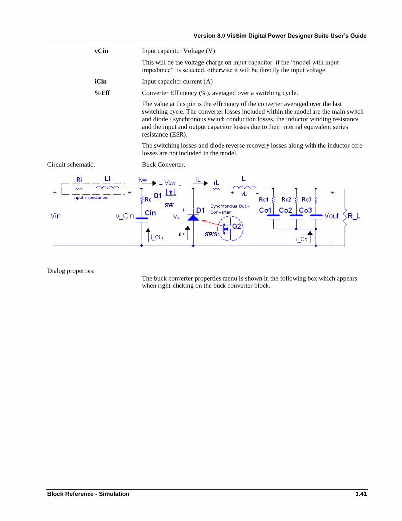
Version 8.0 VisSim Digital Power Designer Suite User’s Guide
Block Reference - Simulation 3.41
vCin Input capacitor Voltage (V)
This will be the voltage charge on input capacitor if the “model with input
impedance” is selected, otherwise it will be directly the input voltage.
iCin Input capacitor current (A)
%Eff Converter Efficiency (%), averaged over a switching cycle.
The value at this pin is the efficiency of the converter averaged over the last
switching cycle. The converter losses included within the model are the main switch
and diode / synchronous switch conduction losses, the inductor winding resistance
and the input and output capacitor losses due to their internal equivalent series
resistance (ESR).
The switching losses and diode reverse recovery losses along with the inductor core
losses are not included in the model.
Circuit schematic: Buck Converter.
Dialog properties:
The buck converter properties menu is shown in the following box which appears
when right-clicking on the buck converter block.

Version 8.0 VisSim Digital Power Designer Suite User’s Guide
3.42 Block Reference - Simulation
Synchronous-rectifier Buck Converter:
When this check box is activated the output diode of the buck converter will be
modelled as a controllable switch (usually a MOSFET). This will activate the SWS
input pin.
Output inductance:
Insert the value of the buck converter output inductance in micro-Henries.
Output inductor internal resistance:
The winding resistance of the buck inductor should be given here in milli-Ohms. The
resistance of any connections can be summed into the given value.
Output capacitance:
Insert the value of the main output capacitor in micro-Farads.
Output capacitor ESR:
The equivalent series resistance (ESR) of the modelled output capacitor should be
given here in milli-Ohms.
Add 2nd
type of output capacitor:
An additional output capacitor (usually of a different type and a different ESR value)
which is connected in parallel with the main capacitor, can be included in the model.
Add 3rd
type of output capacitor:
A third type of output capacitor maybe included.

Version 8.0 VisSim Digital Power Designer Suite User’s Guide
Block Reference - Simulation 3.43
Input capacitance:
The value of the input capacitor in micro-Farads must be given. Note that the actual
capacitance value will only affect the converter performance if “Model with input
impedance” is selected below.
Input capacitor ESR:
Insert the value of the equivalent series resistance of the input capacitor in milli-
Ohms.
Model with input impedance:
Check this box to model the buck converter with input impedance. This can also be
used to model the effects of an input filter on the buck converter.
Input source/line resistance:
Insert the value of the source and / or line resistance in milli-Ohms.
Input source/line inductance:
Insert the value of the source and / or line inductance in nano-Henries.
Power switch voltage drop:
The forward voltage drop, in Volts, across the main switch of the buck converter can
be entered. This value will provide a fixed forward ON-state voltage regardless of
the current flowing through the switch. This value can be combined with the ON-
state resistance below to model an IGBT switch. For a synchronous converter, if the
current through the inductor is negative and both the switches are in the OFF state,
this value will be used as the forward voltage drop of the integrated reverse diode of
the main switch.
Power switch ON-state resistance:
The ON-state resistance, in milli-Ohms, of the main switch can be entered. This
value will model a variable voltage drop dependent upon the current flowing through
the switch such as with a MOSFET.
Diode / Synch. Switch forward voltage drop:
The forward voltage drop, in Volts, across the diode / synchronous switch (in the
case of a synchronous-rectifier converter) of the buck converter can be entered. This
value will provide a fixed forward ON-state voltage regardless of the current flowing
through the diode.
Diode / Synch. Switch ON-state resistance:
The ON-state resistance, in milli-Ohms, of the synchronous switch can be entered. In
the case of synchronous converters where the synchronous rectifier is a MOSFET
switch, the forward voltage across the diode will depend only on this value when the
switch is in the on-state (the SWS control ≥ 1), otherwise it will depend upon the
forward voltage drop only if forward biased and the switch is not controlled.
Import power stage circuit values from file:
The power component values can be directly read from a file. This file is typically
generated by the Power Stage Design Tool within the Digital Power Design Suite.
File path and name:
Enter the full path and name of the file. If only the file name is inserted, it must
reside in the same directory as the main VisSim diagram.
Initial inductor current:
The initial inductor current (at simulation start) can be entered here in Amperes.

Version 8.0 VisSim Digital Power Designer Suite User’s Guide
3.44 Block Reference - Simulation
Inductor roll-off (saturation) knee current:
The converter inductor can be modelled with saturation and this is useful for
inductors constructed with soft magnetic materials. This modelling will produce an
inductor with varying inductance dependent upon the load on the converter.
Inductor saturation roll-off factor:
The roll-off factor of the inductor permeability should be inserted here. For inductors
modelled without saturation, enter a value of zero here.
Output capacitor initial voltage:
The initial voltage of the output capacitor (at simulation start) can be entered here in
Volts.
Include additional converter losses:
The power converter does not model all the component losses and therefore the input
to output efficiency will be higher than expected. Since the converter duty cycle is
inversely proportional to the efficiency as:
(Buck converter, in CCM)
the duty cycle will also be lower than expected. To compensate for this, additional
losses can be introduced when this box is checked.
The figure below shows the variation of duty cycle against efficiency in Continuous
Current Mode (CCM) for different input to output voltage ratios.
Additional losses at nominal load:
Insert the additional full-load losses in Watts.
Additional losses at 10% load:
Insert the additional losses in Watts at 10% of full-load.
DVo
Vi Vi Vo

Version 8.0 VisSim Digital Power Designer Suite User’s Guide
Block Reference - Simulation 3.45
Nominal output voltage:
The nominal output voltage in Volts should be entered into the box. The additional
converter losses included in the model in this case will be constant from zero to 10%
applied load and increase linearly from 10% to the nominal (100%) applied load.
Nominal load resistance:
The nominal (full-load) load resistance must be given here in Ohms.
Set %Load/Io input pin to a load profile (%) input:
Enable this check box to vary the load according to the value at the %Load/Io input
pin and the nominal load resistance.
Set %Load/Io input pin to converter output current (A) input:
Enable this check box to set the load directly to the value of the current input in
amperes. The nominal load resistance is not considered in this case.
Back
Boost Converter
The boost converter is, in its basic form, a second order converter with a non-
inverting output. It is a step-up converter because the output voltage is always higher
than the input voltage when switching.
Input Pins: Vin Input voltage (V)
This is usually connected from a source block or it can be the output of another
converter.
SW Main switch control (SW < 1 = OFF, SW ≥ 1 = ON).
SWS Synchronous switch control (SW < 1 = OFF, SW ≥ 1 = ON).
%Load/Io Proportion of the nominal load in percent or the load current in amperes, depending
upon the configuration of this pin in the block dialog.
This pin controls the amount of load to be applied to the converter at any time
instant. Note that one of the “Set %Load/Io input pin to…” selections must be
checked to enable this pin. The value at this pin is a percentage of the nominal load,
determined by the nominal load resistance value in the dialog (see below) or directly
the load current, depending upon the dialog selection.
Output Pins: Vout Converter output voltage (V)
Iout Converter output current (A)
Iin Converter input current (A). If “model with input impedance” is not selected within
the dialog, then this current will be the average of the input current over each

Version 8.0 VisSim Digital Power Designer Suite User’s Guide
3.46 Block Reference - Simulation
switching period. If the input capacitor is not present (Cin = 0), then this will be the
unfiltered inductor current for the case of the boost converter. Otherwise, the current
will be calculated at each simulation step based upon the input impedance and input
capacitance.
vL Voltage across the inductor (V)
iL Current flowing through the inductor (A)
Vsw Switch Voltage (V) – Positive for forward voltages.
Isw Switch Current (A) – Positive for forward current.
Vd Diode Voltage (V) - Positive for reverse voltages.
The voltage across the output diode / synchronous switch.
Id Diode Current (A) – Positive for forward current.
The current through the output diode / synchronous switch.
iCo Output Capacitor Current (A)
vCin Input capacitor Voltage (V)
This will be the voltage charge on input capacitor if the “model with input
impedance” is selected, otherwise it will be directly the input voltage.
iCin Input capacitor current (A)
%Eff Converter Efficiency (%), averaged over a switching cycle.
The value at this pin is the efficiency of the converter averaged over the last
switching cycle. The converter losses included within the model are the main switch
and diode / synchronous switch conduction losses, the inductor winding resistance
and the input and output capacitor losses due to their internal equivalent series
resistance (ESR).
The switching losses and diode reverse recovery losses along with the inductor core
losses are not included in the model.
Circuit schematic: Boost Converter
Dialog properties:
The boost converter properties menu is shown in the following box which appears
when right-clicking on the boost converter block.
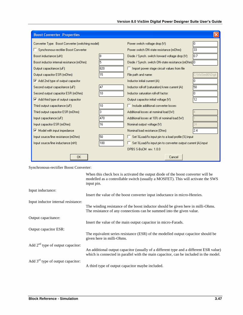
Version 8.0 VisSim Digital Power Designer Suite User’s Guide
Block Reference - Simulation 3.47
Synchronous-rectifier Boost Converter:
When this check box is activated the output diode of the boost converter will be
modelled as a controllable switch (usually a MOSFET). This will activate the SWS
input pin.
Input inductance:
Insert the value of the boost converter input inductance in micro-Henries.
Input inductor internal resistance:
The winding resistance of the boost inductor should be given here in milli-Ohms.
The resistance of any connections can be summed into the given value.
Output capacitance:
Insert the value of the main output capacitor in micro-Farads.
Output capacitor ESR:
The equivalent series resistance (ESR) of the modelled output capacitor should be
given here in milli-Ohms.
Add 2nd
type of output capacitor:
An additional output capacitor (usually of a different type and a different ESR value)
which is connected in parallel with the main capacitor, can be included in the model.
Add 3rd
type of output capacitor:
A third type of output capacitor maybe included.

Version 8.0 VisSim Digital Power Designer Suite User’s Guide
3.48 Block Reference - Simulation
Input capacitance:
The value of the input capacitor in micro-Farads must be given. Note that the actual
capacitance value will only affect the converter performance if “Model with input
impedance” is selected below.
Input capacitor ESR:
Insert the value of the equivalent series resistance of the input capacitor in milli-
Ohms.
Model with input impedance:
Check this box to include the input impedance in the boost converter model. This can
also be used to model the effects of an input filter in the boost converter.
Input source/line resistance:
Insert the value of the source and / or line resistance in milli-Ohms.
Input source/line inductance:
Insert the value of the source and / or line inductance in nano-Henries.
Power switch voltage drop:
The forward voltage drop, in Volts, across the main switch of the boost converter can
be entered. This value will provide a fixed forward ON-state voltage regardless of
the current flowing through the switch. This value can be combined with the ON-
state resistance below to model an IGBT switch. For a synchronous converter, if the
current through the inductor is negative and both the switches are in the OFF state,
this value will be used as the forward voltage drop of the integrated reverse diode of
the main switch.
Power switch ON-state resistance:
The ON-state resistance, in milli-Ohms, of the main switch can be entered. This
value will model a variable voltage drop dependent upon the current flowing through
the switch such as with a MOSFET.
Diode / Synch. Switch forward voltage drop:
The forward voltage drop, in Volts, across the diode / synchronous switch (in the
case of a synchronous-rectifier converter) of the boost converter can be entered. This
value will provide a fixed forward ON-state voltage regardless of the current flowing
through the diode.
Diode / Synch. Switch ON-state resistance:
The ON-state resistance, in milli-Ohms, of the synchronous switch can be entered. In
the case of synchronous converters where the synchronous rectifier is a MOSFET
switch, the forward voltage across the diode will depend only on this value when the
switch is in the on-state (the SWS control ≥ 1), otherwise it will depend upon the
forward voltage drop only if forward biased and the switch is not controlled.
Import power stage circuit values from file:
The power component values can be directly read from a file. This file is typically
generated by the Power Stage Design Tool within the Digital Power Design Suite.
File path and name:
Enter the full path and name of the file. If only the file name is inserted, it must
reside in the same directory as the main VisSim diagram.
Initial inductor current:
The initial inductor current (at simulation start) can be entered here in Amperes.
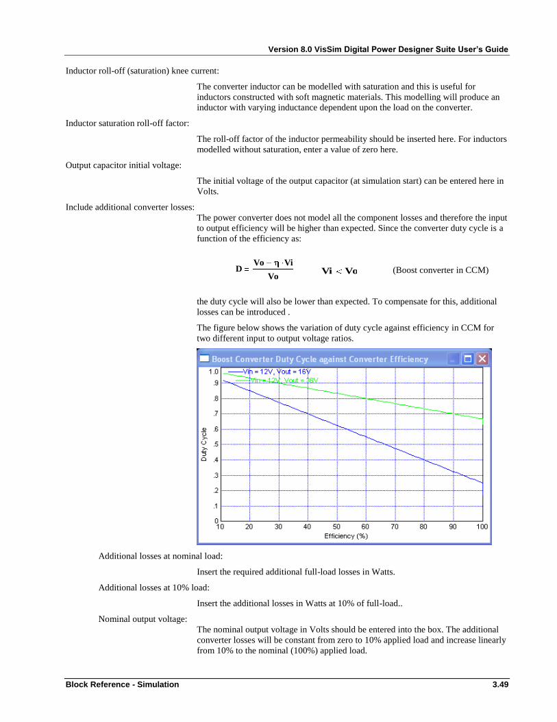
Version 8.0 VisSim Digital Power Designer Suite User’s Guide
Block Reference - Simulation 3.49
Inductor roll-off (saturation) knee current:
The converter inductor can be modelled with saturation and this is useful for
inductors constructed with soft magnetic materials. This modelling will produce an
inductor with varying inductance dependent upon the load on the converter.
Inductor saturation roll-off factor:
The roll-off factor of the inductor permeability should be inserted here. For inductors
modelled without saturation, enter a value of zero here.
Output capacitor initial voltage:
The initial voltage of the output capacitor (at simulation start) can be entered here in
Volts.
Include additional converter losses:
The power converter does not model all the component losses and therefore the input
to output efficiency will be higher than expected. Since the converter duty cycle is a
function of the efficiency as:
(Boost converter in CCM)
the duty cycle will also be lower than expected. To compensate for this, additional
losses can be introduced .
The figure below shows the variation of duty cycle against efficiency in CCM for
two different input to output voltage ratios.
Additional losses at nominal load:
Insert the required additional full-load losses in Watts.
Additional losses at 10% load:
Insert the additional losses in Watts at 10% of full-load..
Nominal output voltage:
The nominal output voltage in Volts should be entered into the box. The additional
converter losses will be constant from zero to 10% applied load and increase linearly
from 10% to the nominal (100%) applied load.
DVo Vi
Vo Vi Vo
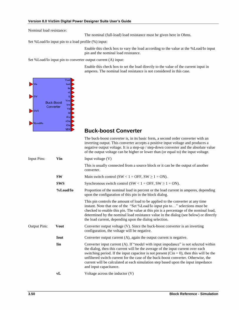
Version 8.0 VisSim Digital Power Designer Suite User’s Guide
3.50 Block Reference - Simulation
Nominal load resistance:
The nominal (full-load) load resistance must be given here in Ohms.
Set %Load/Io input pin to a load profile (%) input:
Enable this check box to vary the load according to the value at the %Load/Io input
pin and the nominal load resistance.
Set %Load/Io input pin to converter output current (A) input:
Enable this check box to set the load directly to the value of the current input in
amperes. The nominal load resistance is not considered in this case.
Buck-boost Converter
The buck-boost converter is, in its basic form, a second order converter with an
inverting output. This converter accepts a positive input voltage and produces a
negative output voltage. It is a step-up / step-down converter and the absolute value
of the output voltage can be higher or lower than (or equal to) the input voltage.
Input Pins: Vin Input voltage (V)
This is usually connected from a source block or it can be the output of another
converter.
SW Main switch control (SW < 1 = OFF, SW ≥ 1 = ON).
SWS Synchronous switch control (SW < 1 = OFF, SW ≥ 1 = ON).
%Load/Io Proportion of the nominal load in percent or the load current in amperes, depending
upon the configuration of this pin in the block dialog.
This pin controls the amount of load to be applied to the converter at any time
instant. Note that one of the “Set %Load/Io input pin to…” selections must be
checked to enable this pin. The value at this pin is a percentage of the nominal load,
determined by the nominal load resistance value in the dialog (see below) or directly
the load current, depending upon the dialog selection.
Output Pins: Vout Converter output voltage (V). Since the buck-boost converter is an inverting
configuration, the voltage will be negative.
Iout Converter output current (A), again the output current is negative.
Iin Converter input current (A). If “model with input impedance” is not selected within
the dialog, then this current will be the average of the input current over each
switching period. If the input capacitor is not present (Cin = 0), then this will be the
unfiltered switch current for the case of the buck-boost converter. Otherwise, the
current will be calculated at each simulation step based upon the input impedance
and input capacitance.
vL Voltage across the inductor (V)
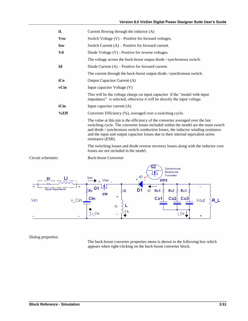
Version 8.0 VisSim Digital Power Designer Suite User’s Guide
Block Reference - Simulation 3.51
iL Current flowing through the inductor (A)
Vsw Switch Voltage (V) – Positive for forward voltages.
Isw Switch Current (A) – Positive for forward current.
Vd Diode Voltage (V) - Positive for reverse voltages.
The voltage across the buck-boost output diode / synchronous switch.
Id Diode Current (A) – Positive for forward current.
The current through the buck-boost output diode / synchronous switch.
iCo Output Capacitor Current (A)
vCin Input capacitor Voltage (V)
This will be the voltage charge on input capacitor if the “model with input
impedance” is selected, otherwise it will be directly the input voltage.
iCin Input capacitor current (A)
%Eff Converter Efficiency (%), averaged over a switching cycle.
The value at this pin is the efficiency of the converter averaged over the last
switching cycle. The converter losses included within the model are the main switch
and diode / synchronous switch conduction losses, the inductor winding resistance
and the input and output capacitor losses due to their internal equivalent series
resistance (ESR).
The switching losses and diode reverse recovery losses along with the inductor core
losses are not included in the model.
Circuit schematic: Buck-boost Converter
Dialog properties:
The buck-boost converter properties menu is shown in the following box which
appears when right-clicking on the buck-boost converter block.
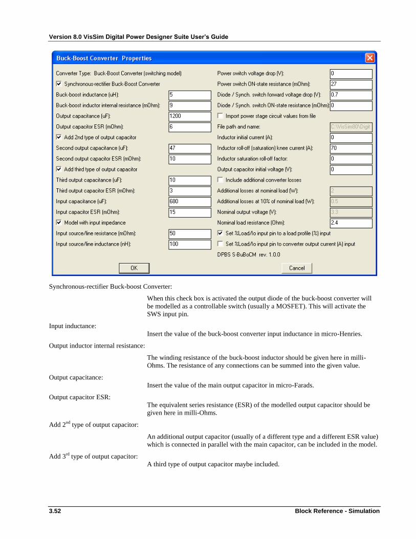
Version 8.0 VisSim Digital Power Designer Suite User’s Guide
3.52 Block Reference - Simulation
Synchronous-rectifier Buck-boost Converter:
When this check box is activated the output diode of the buck-boost converter will
be modelled as a controllable switch (usually a MOSFET). This will activate the
SWS input pin.
Input inductance:
Insert the value of the buck-boost converter input inductance in micro-Henries.
Output inductor internal resistance:
The winding resistance of the buck-boost inductor should be given here in milli-
Ohms. The resistance of any connections can be summed into the given value.
Output capacitance:
Insert the value of the main output capacitor in micro-Farads.
Output capacitor ESR:
The equivalent series resistance (ESR) of the modelled output capacitor should be
given here in milli-Ohms.
Add 2nd
type of output capacitor:
An additional output capacitor (usually of a different type and a different ESR value)
which is connected in parallel with the main capacitor, can be included in the model.
Add 3rd
type of output capacitor:
A third type of output capacitor maybe included.

Version 8.0 VisSim Digital Power Designer Suite User’s Guide
Block Reference - Simulation 3.53
Input capacitance:
The value of the input capacitor in micro-Farads must be given. Note that the actual
capacitance value will only affect the converter performance if “Model with input
impedance” is selected below.
Input capacitor ESR:
Insert the value of the equivalent series resistance of the input capacitor in milli-
Ohms.
Model with input impedance:
Check this box to include the input impedance in the buck-boost converter model.
This can also be used to model the effects of an input filter in the buck-boost
converter.
Input source/line resistance:
Insert the value of the source and / or line resistance in milli-Ohms.
Input source/line inductance:
Insert the value of the source and / or line inductance in nano-Henries.
Power switch voltage drop:
The forward voltage drop, in Volts, across the main switch of the buck-boost
converter can be entered. This value will provide a fixed forward ON-state voltage
regardless of the current flowing through the switch. This value can be combined
with the ON-state resistance below to model an IGBT switch. For a synchronous
converter, if the current through the inductor is negative and both the switches are in
the OFF state, this value will be used as the forward voltage drop of the integrated
reverse diode of the main switch.
Power switch ON-state resistance:
The ON-state resistance, in milli-Ohms, of the main switch can be entered. This
value will model a variable voltage drop dependent upon the current flowing through
the switch such as with a MOSFET.
Diode / Synch. Switch forward voltage drop:
The forward voltage drop, in Volts, across the diode / synchronous switch (in the
case of a synchronous-rectifier converter) of the buck-boost converter can be
entered. This value will provide a fixed forward ON-state voltage regardless of the
current flowing through the diode.
Diode / Synch. Switch ON-state resistance:
The ON-state resistance, in milli-Ohms, of the synchronous switch can be entered. In
the case of synchronous converters where the synchronous rectifier is a MOSFET
switch, the forward voltage across the diode will depend only on this value when the
switch is in the on-state (the SWS control ≥ 1), otherwise it will depend upon the
forward voltage drop only if forward biased and the switch is not controlled.
Import power stage circuit values from file:
The power component values can be directly read from a file. This file is typically
generated by the Power Stage Design Tool within the Digital Power Designer Suite.
File path and name:
Enter the full path and name of the file. If only the file name is inserted, it must
reside in the same directory as the main VisSim diagram.
Initial inductor current:
The initial inductor current (at simulation start) can be entered here in Amperes.

Version 8.0 VisSim Digital Power Designer Suite User’s Guide
3.54 Block Reference - Simulation
Inductor roll-off (saturation) knee current:
The converter inductor can be modelled with saturation and this is useful for
inductors constructed with soft magnetic materials. This modelling will produce an
inductor with varying inductance dependent upon the current flowing through the
inductor.
Inductor saturation roll-off factor:
The roll-off factor of the inductor permeability should be inserted here. For inductors
modelled without saturation, enter a value of zero here.
Output capacitor initial voltage:
The initial voltage of the output capacitor (at simulation start) can be entered here in
Volts.
Include additional converter losses:
The power converter does not model all the component losses and therefore the input
to output efficiency will be higher than expected. Since the converter duty cycle is a
function of the efficiency as:
(Buck-boost converter in CCM)
the duty cycle will also be lower than expected. To compensate for this, additional
losses can be introduced . The figure below shows the variation of duty cycle against
efficiency in CCM for different input to output voltage ratios for the buck-boost
converter.
Additional losses at nominal load:
Insert the required additional full-load losses in Watts.
Additional losses at 10% load:
Insert the additional losses in Watts at 10% of full-load..
Nominal output voltage:
DVo
Vi Vo
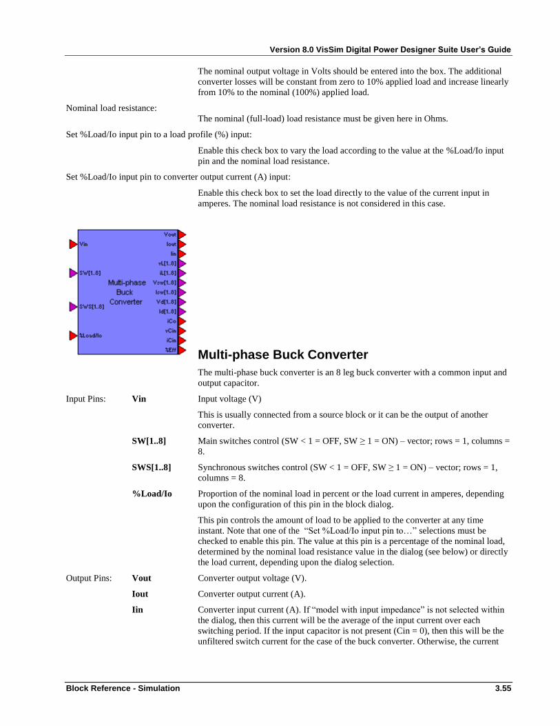
Version 8.0 VisSim Digital Power Designer Suite User’s Guide
Block Reference - Simulation 3.55
The nominal output voltage in Volts should be entered into the box. The additional
converter losses will be constant from zero to 10% applied load and increase linearly
from 10% to the nominal (100%) applied load.
Nominal load resistance:
The nominal (full-load) load resistance must be given here in Ohms.
Set %Load/Io input pin to a load profile (%) input:
Enable this check box to vary the load according to the value at the %Load/Io input
pin and the nominal load resistance.
Set %Load/Io input pin to converter output current (A) input:
Enable this check box to set the load directly to the value of the current input in
amperes. The nominal load resistance is not considered in this case.
Multi-phase Buck Converter
The multi-phase buck converter is an 8 leg buck converter with a common input and
output capacitor.
Input Pins: Vin Input voltage (V)
This is usually connected from a source block or it can be the output of another
converter.
SW[1..8] Main switches control (SW < 1 = OFF, SW ≥ 1 = ON) – vector; rows = 1, columns =
8.
SWS[1..8] Synchronous switches control (SW < 1 = OFF, SW ≥ 1 = ON) – vector; rows = 1,
columns = 8.
%Load/Io Proportion of the nominal load in percent or the load current in amperes, depending
upon the configuration of this pin in the block dialog.
This pin controls the amount of load to be applied to the converter at any time
instant. Note that one of the “Set %Load/Io input pin to…” selections must be
checked to enable this pin. The value at this pin is a percentage of the nominal load,
determined by the nominal load resistance value in the dialog (see below) or directly
the load current, depending upon the dialog selection.
Output Pins: Vout Converter output voltage (V).
Iout Converter output current (A).
Iin Converter input current (A). If “model with input impedance” is not selected within
the dialog, then this current will be the average of the input current over each
switching period. If the input capacitor is not present (Cin = 0), then this will be the
unfiltered switch current for the case of the buck converter. Otherwise, the current
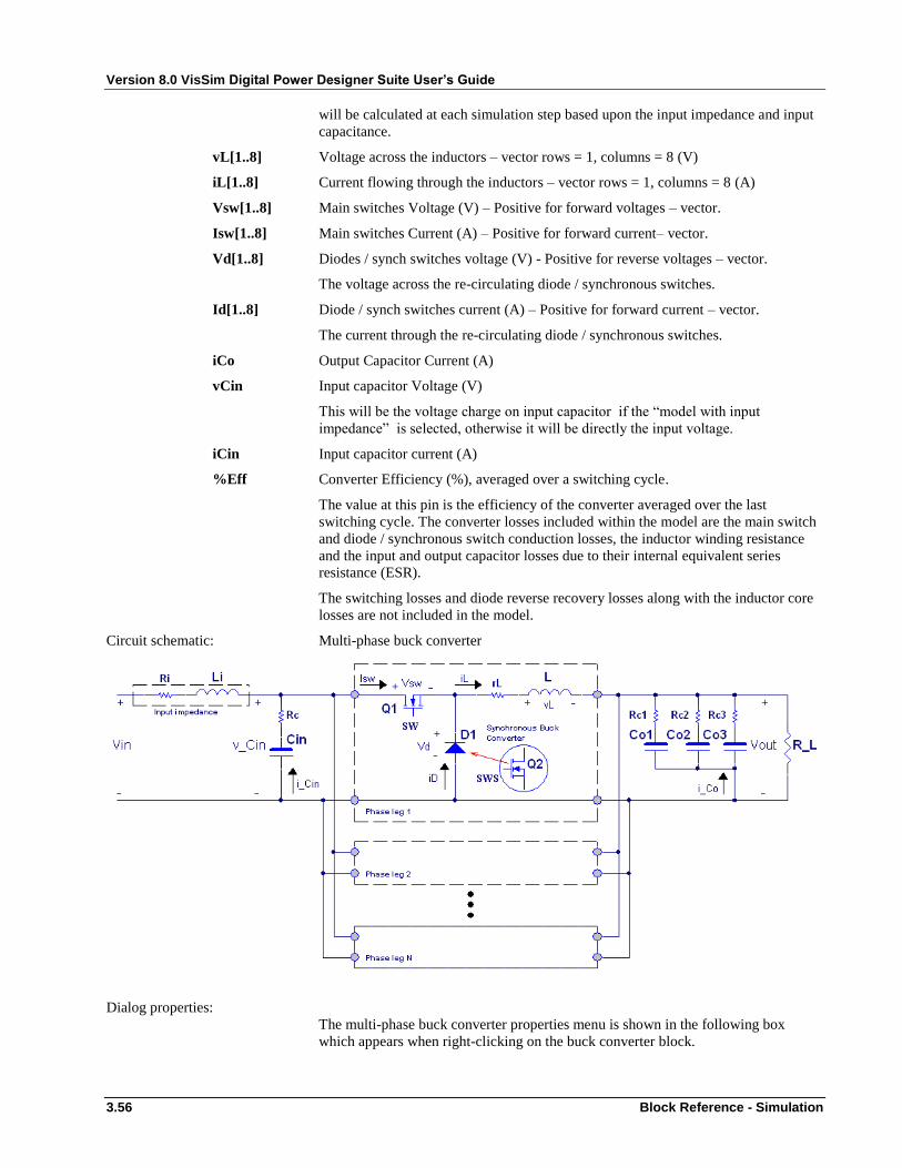
Version 8.0 VisSim Digital Power Designer Suite User’s Guide
3.56 Block Reference - Simulation
will be calculated at each simulation step based upon the input impedance and input
capacitance.
vL[1..8] Voltage across the inductors – vector rows = 1, columns = 8 (V)
iL[1..8] Current flowing through the inductors – vector rows = 1, columns = 8 (A)
Vsw[1..8] Main switches Voltage (V) – Positive for forward voltages – vector.
Isw[1..8] Main switches Current (A) – Positive for forward current– vector.
Vd[1..8] Diodes / synch switches voltage (V) - Positive for reverse voltages – vector.
The voltage across the re-circulating diode / synchronous switches.
Id[1..8] Diode / synch switches current (A) – Positive for forward current – vector.
The current through the re-circulating diode / synchronous switches.
iCo Output Capacitor Current (A)
vCin Input capacitor Voltage (V)
This will be the voltage charge on input capacitor if the “model with input
impedance” is selected, otherwise it will be directly the input voltage.
iCin Input capacitor current (A)
%Eff Converter Efficiency (%), averaged over a switching cycle.
The value at this pin is the efficiency of the converter averaged over the last
switching cycle. The converter losses included within the model are the main switch
and diode / synchronous switch conduction losses, the inductor winding resistance
and the input and output capacitor losses due to their internal equivalent series
resistance (ESR).
The switching losses and diode reverse recovery losses along with the inductor core
losses are not included in the model.
Circuit schematic: Multi-phase buck converter
Dialog properties:
The multi-phase buck converter properties menu is shown in the following box
which appears when right-clicking on the buck converter block.
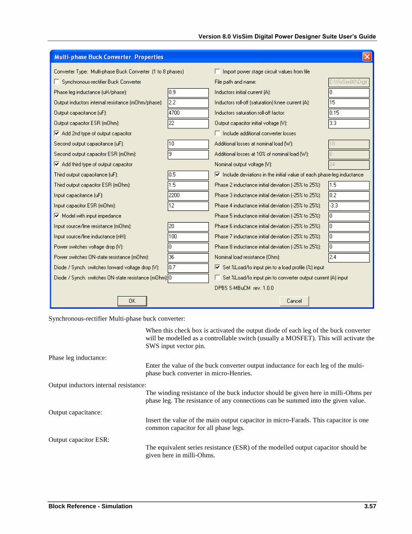
Version 8.0 VisSim Digital Power Designer Suite User’s Guide
Block Reference - Simulation 3.57
Synchronous-rectifier Multi-phase buck converter:
When this check box is activated the output diode of each leg of the buck converter
will be modelled as a controllable switch (usually a MOSFET). This will activate the
SWS input vector pin.
Phase leg inductance:
Enter the value of the buck converter output inductance for each leg of the multi-
phase buck converter in micro-Henries.
Output inductors internal resistance:
The winding resistance of the buck inductor should be given here in milli-Ohms per
phase leg. The resistance of any connections can be summed into the given value.
Output capacitance:
Insert the value of the main output capacitor in micro-Farads. This capacitor is one
common capacitor for all phase legs.
Output capacitor ESR:
The equivalent series resistance (ESR) of the modelled output capacitor should be
given here in milli-Ohms.
Version 8.0 VisSim Digital Power Designer Suite User’s Guide
3.58 Block Reference - Simulation
Add 2nd
type of output capacitor:
An additional output capacitor (usually of a different type and a different ESR value)
which is connected in parallel with the main capacitor, can be included in the model.
Add 3rd
type of output capacitor:
A third type of output capacitor maybe included.
Input capacitance:
The value of the input capacitor in micro-Farads must be given. Note that the actual
capacitance value will only affect the converter performance if “Model with input
impedance” is selected below.
Input capacitor ESR:
Insert the value of the equivalent series resistance of the input capacitor in milli-
Ohms.
Model with input impedance:
Check this box to model the multi-phase buck converter with input impedance. This
can also be used to model the effects of an input filter on the converter.
Input source/line resistance:
Insert the value of the source and / or line resistance in milli-Ohms.
Input source/line inductance:
Insert the value of the source and / or line inductance in nano-Henries.
Power switch voltage drop:
The forward voltage drop, in Volts, across the main switch of each leg of the buck
converter can be entered. This value will provide a fixed forward ON-state voltage
regardless of the current flowing through the switch. This value can be combined
with the ON-state resistance below to model an IGBT switch. For a synchronous
converter, if the current through the inductor is negative and both the switches are in
the OFF state, this value will be used as the forward voltage drop of the integrated
reverse diode of the main switch.
Power switch ON-state resistance:
The ON-state resistance, in milli-Ohms, of the main switch can be entered. This
value will model a variable voltage drop dependent upon the current flowing through
the switch such as with a MOSFET.
Diode / Synch. Switch forward voltage drop:
The forward voltage drop, in Volts, across the diode / synchronous switch (in the
case of a synchronous-rectifier converter) of each leg of the multi-phase buck
converter can be entered. This value will provide a fixed forward ON-state voltage
regardless of the current flowing through the diode.
Diode / Synch. Switch ON-state resistance:
The ON-state resistance, in milli-Ohms, of the synchronous switch can be entered. In
the case of synchronous converters where the synchronous rectifier is a MOSFET
switch, the forward voltage across the diode will depend only on this value when the
switch is in the on-state (the SWS control ≥ 1), otherwise it will depend upon the
forward voltage drop only if forward biased and the switch is not controlled.
Import power stage circuit values from file:
The power component values can be directly read from a file. This file is typically
generated by the Power Stage Design Tool within the Digital Power Design Suite.
Version 8.0 VisSim Digital Power Designer Suite User’s Guide
Block Reference - Simulation 3.59
File path and name:
Enter the full path and name of the file. If only the file name is inserted, it must
reside in the same directory as the main VisSim diagram.
Initial inductor current:
The initial inductor current (at simulation start) can be entered here in Amperes.
Inductor roll-off (saturation) knee current:
The converter inductor can be modelled with saturation and this is useful for
inductors constructed with soft magnetic materials. This modelling will produce an
inductor with varying inductance dependent upon the load on the converter.
Inductor saturation roll-off factor:
The roll-off factor of the inductor permeability should be inserted here. For inductors
modelled without saturation, enter a value of zero here.
Output capacitor initial voltage:
The initial voltage of the output capacitor (at simulation start) can be entered here in
Volts.
Include additional converter losses:
The power converter does not model all the component losses and therefore the input
to output efficiency will be higher than expected. Since the converter duty cycle is
inversely proportional to the efficiency as:
(Buck converter in CCM)
the duty cycle will also be lower than expected. To compensate for this, additional
losses can be introduced when this box is checked.
Additional losses at nominal load:
Insert the additional full-load losses in Watts.
Additional losses at 10% load:
Insert the additional losses in Watts at 10% of full-load.
Nominal output voltage:
The nominal output voltage in Volts should be entered into the box. The additional
converter losses will be constant from zero to 10% applied load and increase linearly
from 10% to the nominal (100%) applied load.
Include deviations in the initial value of each phase leg inductance:
The value of the inductor of each phase leg will never be identical in practise and
deviations of the initial inductance can be accounted for by checking this box.
Phase x inductance initial deviation:
For each phase, enter the desired deviation of the initial inductance within ±25% of
the nominal value.
Nominal load resistance:
The nominal (full-load) load resistance must be given here in Ohms.
Set %Load/Io input pin to a load profile (%) input:
Enable this check box to vary the load according to the value at the %Load/Io input
pin and the nominal load resistance.
Vi Vo DVo
Vi

Version 8.0 VisSim Digital Power Designer Suite User’s Guide
3.60 Block Reference - Simulation
Set %Load/Io input pin to converter output current (A) input:
Enable this check box to set the load directly to the value of the current input in
amperes. The nominal load resistance is not considered in this case.
Back
Multi-phase Boost Converter
The multi-phase boost converter is an 8 leg boost converter with a common input
and output capacitor.
Input Pins: Vin Input voltage (V)
This is usually connected from a source block or it can be the output of another
converter.
SW1..8 Main switches control (SW < 1 = OFF, SW ≥ 1 = ON) – vector; rows = 1, columns =
8.
SWS1..8 Synchronous switches control (SW < 1 = OFF, SW ≥ 1 = ON) – vector; rows = 1,
columns = 8.
%Load/Io Proportion of the nominal load in percent or the load current in amperes, depending
upon the configuration of this pin in the block dialog.
This pin controls the amount of load to be applied to the converter at any time
instant. Note that one of the “Set %Load/Io input pin to…” selections must be
checked to enable this pin. The value at this pin is a percentage of the nominal load,
determined by the nominal load resistance value in the dialog (see below) or directly
the load current, depending upon the dialog selection.
Output Pins: Vout Converter output voltage (V)
Iout Converter output current (A)
Iin Converter input current (A). If “model with input impedance” is not selected within
the dialog, then this current will be the average of the input current over each
switching period. If the input capacitor is not present (Cin = 0), then this will be the
unfiltered switch current for the case of the boost converter. Otherwise, the current
will be calculated at each simulation step based upon the input impedance and input
capacitance.
vL1..8 Voltage across the inductors (V) – vector rows = 1, columns = 8
iL1..8 Current flowing through the inductors (A) – vector rows = 1, columns = 8
Vsw1..8 Main switches Voltage (V) – Positive for forward voltages – vector.
Isw1..8 Main switches Current (A) – Positive for forward current– vector.

Version 8.0 VisSim Digital Power Designer Suite User’s Guide
Block Reference - Simulation 3.61
Vd1..8 Diodes / synch switches voltage (V) - Positive for reverse voltages – vector.
The voltage across the boost output diode / synchronous switch.
Id1..8 Diode / synch switches current (A) – Positive for forward current – vector.
The current through the boost output diode / synchronous switch.
iCo Output Capacitor Current (A)
vCin Input capacitor Voltage (V)
iCin Input capacitor current (A)
%Eff Converter Efficiency (%), averaged over a switching cycle.
Circuit schematic: Multi-phase boost converter
Dialog properties:
The multi-phase boost converter properties menu is shown in the following box
which appears when right-clicking on the converter block.

Version 8.0 VisSim Digital Power Designer Suite User’s Guide
3.62 Block Reference - Simulation
The dialogs are very similar to the multi-phase buck converter and the boost
converter.
Back

Version 8.0 VisSim Digital Power Designer Suite User’s Guide
Block Reference - Simulation 3.63
Multi-phase Buck-boost Converter
The multi-phase buck-boost converter is an 8 leg inverting (positive input, negative
output) buck-boost converter with a common input and output capacitor.
Input Pins: Vin Input voltage (V)
SW1..8 Main switches control (SW < 1 = OFF, SW ≥ 1 = ON) – vector; rows = 1, columns =
8.
SWS1..8 Synchronous switches control (SW < 1 = OFF, SW ≥ 1 = ON) – vector; rows = 1,
columns = 8.
%Load/Io Proportion of the nominal load in percent or the load current in amperes, depending
upon the configuration of this pin in the block dialog.
This pin controls the amount of load to be applied to the converter at any time
instant. Note that one of the “Set %Load/Io input pin to…” selections must be
checked to enable this pin. The value at this pin is a percentage of the nominal load,
determined by the nominal load resistance value in the dialog (see below) or directly
the load current, depending upon the dialog selection.
Output Pins: Vout Converter output voltage (V)
Iout Converter output current (A)
Iin Converter input current (A). If “model with input impedance” is not selected within
the dialog, then this current will be the average of the input current over each
switching period. If the input capacitor is not present (Cin = 0), then this will be the
unfiltered switch current for the case of the buck-boost converter. Otherwise, the
current will be calculated at each simulation step based upon the input impedance
and input capacitance.
vL1..8 Voltage across the inductors – vector rows = 1, columns = 8 (V).
iL1..8 Current flowing through the inductors – vector rows = 1, columns = 8 (A)
Vsw1..8 Main switches Voltage (V) – Positive for forward voltages – vector.
Isw1..8 Main switches Current (A) – Positive for forward current– vector.
Vd1..8 Diodes / synch switches voltage (V) - Positive for reverse voltages – vector.
The voltage across the buck-boost output diode / synchronous switch.
Id1..8 Diode / synch switches current (A) – Positive for forward current – vector.
The current through the buck-boost output diode / synchronous switch.
iCo Output Capacitor Current (A)
vCin Input capacitor Voltage (V)
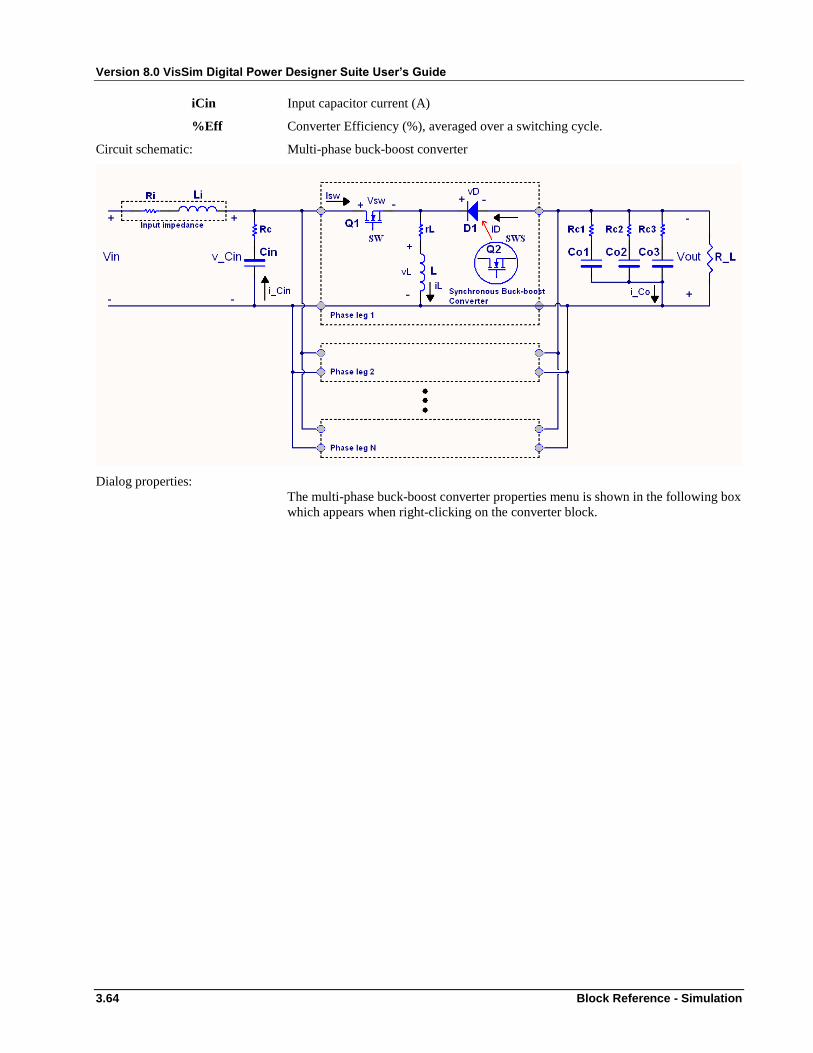
Version 8.0 VisSim Digital Power Designer Suite User’s Guide
3.64 Block Reference - Simulation
iCin Input capacitor current (A)
%Eff Converter Efficiency (%), averaged over a switching cycle.
Circuit schematic: Multi-phase buck-boost converter
Dialog properties:
The multi-phase buck-boost converter properties menu is shown in the following box
which appears when right-clicking on the converter block.
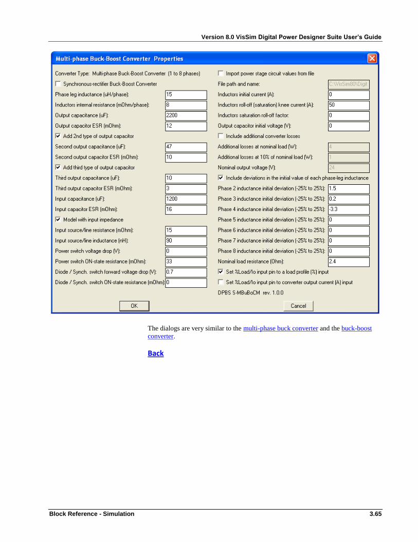
Version 8.0 VisSim Digital Power Designer Suite User’s Guide
Block Reference - Simulation 3.65
The dialogs are very similar to the multi-phase buck converter and the buck-boost
converter.
Back
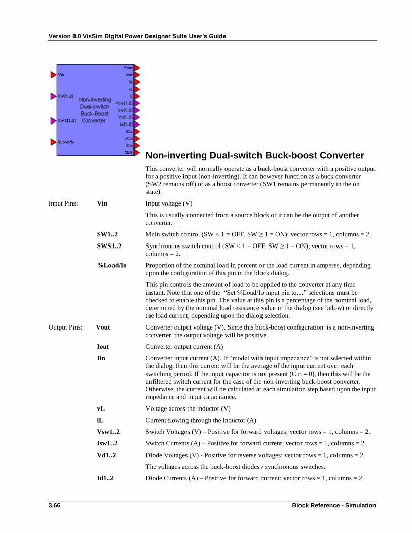
Version 8.0 VisSim Digital Power Designer Suite User’s Guide
3.66 Block Reference - Simulation
Non-inverting Dual-switch Buck-boost Converter
This converter will normally operate as a buck-boost converter with a positive output
for a positive input (non-inverting). It can however function as a buck converter
(SW2 remains off) or as a boost converter (SW1 remains permanently in the on
state).
Input Pins: Vin Input voltage (V)
This is usually connected from a source block or it can be the output of another
converter.
SW1..2 Main switch control (SW < 1 = OFF, SW ≥ 1 = ON); vector rows = 1, columns = 2.
SWS1..2 Synchronous switch control (SW < 1 = OFF, SW ≥ 1 = ON); vector rows = 1,
columns = 2.
%Load/Io Proportion of the nominal load in percent or the load current in amperes, depending
upon the configuration of this pin in the block dialog.
This pin controls the amount of load to be applied to the converter at any time
instant. Note that one of the “Set %Load/Io input pin to…” selections must be
checked to enable this pin. The value at this pin is a percentage of the nominal load,
determined by the nominal load resistance value in the dialog (see below) or directly
the load current, depending upon the dialog selection.
Output Pins: Vout Converter output voltage (V). Since this buck-boost configuration is a non-inverting
converter, the output voltage will be positive.
Iout Converter output current (A)
Iin Converter input current (A). If “model with input impedance” is not selected within
the dialog, then this current will be the average of the input current over each
switching period. If the input capacitor is not present (Cin = 0), then this will be the
unfiltered switch current for the case of the non-inverting buck-boost converter.
Otherwise, the current will be calculated at each simulation step based upon the input
impedance and input capacitance.
vL Voltage across the inductor (V)
iL Current flowing through the inductor (A)
Vsw1..2 Switch Voltages (V) – Positive for forward voltages; vector rows = 1, columns = 2.
Isw1..2 Switch Currents (A) – Positive for forward current; vector rows = 1, columns = 2.
Vd1..2 Diode Voltages (V) - Positive for reverse voltages; vector rows = 1, columns = 2.
The voltages across the buck-boost diodes / synchronous switches.
Id1..2 Diode Currents (A) – Positive for forward current; vector rows = 1, columns = 2.

Version 8.0 VisSim Digital Power Designer Suite User’s Guide
Block Reference - Simulation 3.67
The current through the buck-boost output diode / synchronous switches.
iCo Output Capacitor Current (A)
vCin Input capacitor Voltage (V)
This will be the voltage charge on input capacitor if the “model with input
impedance” is selected, otherwise it will be directly the input voltage.
iCin Input capacitor current (A)
%Eff Converter Efficiency (%), averaged over a switching cycle.
The value at this pin is the efficiency of the converter averaged over the last
switching cycle. The converter losses included within the model are the main switch
and diode / synchronous switch conduction losses, the inductor winding resistance
and the input and output capacitor losses due to their internal equivalent series
resistance (ESR).
The switching losses and diode reverse recovery losses along with the inductor core
losses are not included in the model.
Circuit schematic: Non-inverting dual-switch buck-boost converter
Dialog properties:
The non-inverting, dual-switch buck-boost converter properties menu is shown in the
following box which appears when right-clicking on the buck-boost converter block.
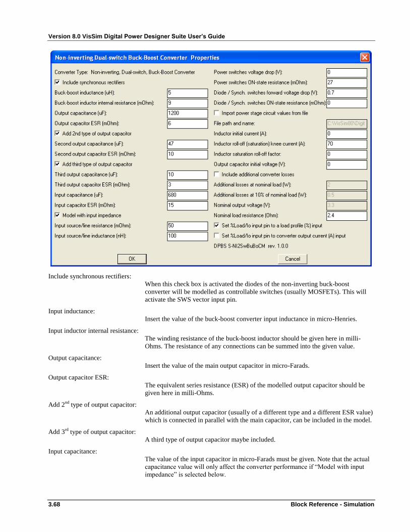
Version 8.0 VisSim Digital Power Designer Suite User’s Guide
3.68 Block Reference - Simulation
Include synchronous rectifiers:
When this check box is activated the diodes of the non-inverting buck-boost
converter will be modelled as controllable switches (usually MOSFETs). This will
activate the SWS vector input pin.
Input inductance:
Insert the value of the buck-boost converter input inductance in micro-Henries.
Input inductor internal resistance:
The winding resistance of the buck-boost inductor should be given here in milli-
Ohms. The resistance of any connections can be summed into the given value.
Output capacitance:
Insert the value of the main output capacitor in micro-Farads.
Output capacitor ESR:
The equivalent series resistance (ESR) of the modelled output capacitor should be
given here in milli-Ohms.
Add 2nd
type of output capacitor:
An additional output capacitor (usually of a different type and a different ESR value)
which is connected in parallel with the main capacitor, can be included in the model.
Add 3rd
type of output capacitor:
A third type of output capacitor maybe included.
Input capacitance:
The value of the input capacitor in micro-Farads must be given. Note that the actual
capacitance value will only affect the converter performance if “Model with input
impedance” is selected below.
Version 8.0 VisSim Digital Power Designer Suite User’s Guide
Block Reference - Simulation 3.69
Input capacitor ESR:
Insert the value of the equivalent series resistance of the input capacitor in milli-
Ohms.
Model with input impedance:
Check this box to include the input impedance in the buck-boost converter model.
This can also be used to model the effects of an input filter in the buck-boost
converter.
Input source/line resistance:
Insert the value of the source and / or line resistance in milli-Ohms.
Input source/line inductance:
Insert the value of the source and / or line inductance in nano-Henries.
Power switches voltage drop:
The forward voltage drop, in Volts, across the main switch of the boost converter can
be entered. This value will provide a fixed forward ON-state voltage regardless of
the current flowing through the switch. This value can be combined with the ON-
state resistance below to model an IGBT switch. For a synchronous converter, if the
current through the inductor is negative and both the switches are in the OFF state,
this value will be used as the forward voltage drop of the integrated reverse diode of
the main switch.
Power switches ON-state resistance:
The ON-state resistance, in milli-Ohms, of the main switch can be entered. This
value will model a variable voltage drop dependent upon the current flowing through
the switch such as with a MOSFET.
Diodes / Synch. Switches forward voltage drop:
The forward voltage drop, in Volts, across the diodes / synchronous switches (in the
case of a synchronous-rectifier converter) of the non-inverting buck-boost converter
can be entered. This value will provide a fixed forward ON-state voltage regardless
of the current flowing through the diode.
Diodes / Synch. Switches ON-state resistance:
The ON-state resistance, in milli-Ohms, of the synchronous switch can be entered. In
the case of synchronous converters where the synchronous rectifier is a MOSFET
switch, the forward voltage across the diode will depend only on this value when the
switch is in the on-state (the SWS control ≥ 1), otherwise it will depend upon the
forward voltage drop only if forward biased and the switch is not controlled.
Import power stage circuit values from file:
The power component values can be directly read from a file.
File path and name:
Enter the full path and name of the file. If only the file name is inserted, it must
reside in the same directory as the main VisSim diagram.
Initial inductor current:
The initial inductor current (at simulation start) can be entered here in Amperes.
Inductor roll-off (saturation) knee current:
The converter inductor can be modelled with saturation and this is useful for
inductors constructed with soft magnetic materials. This modelling will produce an
inductor with varying inductance dependent upon the current flowing through the
inductor.

Version 8.0 VisSim Digital Power Designer Suite User’s Guide
3.70 Block Reference - Simulation
Inductor saturation roll-off factor:
The roll-off factor of the inductor permeability should be inserted here. For inductors
modelled without saturation, enter a value of zero here.
Output capacitor initial voltage:
The initial voltage of the output capacitor (at simulation start) can be entered here in
Volts.
Include additional converter losses:
The power converter does not model all the component losses and therefore the input
to output efficiency will be higher than expected. Since the converter duty cycle is a
function of the efficiency as:
(Buck-boost converter in CCM)
the duty cycle will also be lower than expected. To compensate for this, additional
losses can be introduced .
Additional losses at nominal load:
Insert the required additional full-load losses in Watts.
Additional losses at 10% load:
Insert the additional losses in Watts at 10% of full-load..
Nominal output voltage:
The nominal output voltage in Volts should be entered into the box. The additional
converter losses will be constant from zero to 10% applied load and increase linearly
from 10% to the nominal (100%) applied load.
Nominal load resistance:
The nominal (full-load) load resistance must be given here in Ohms.
Set %Load/Io input pin to a load profile (%) input:
Enable this check box to vary the load according to the value at the %Load/Io input
pin and the nominal load resistance.
Set %Load/Io input pin to converter output current (A) input:
Enable this check box to set the load directly to the value of the current input in
amperes. The nominal load resistance is not considered in this case.
Back
DVo
Vi Vo

Version 8.0 VisSim Digital Power Designer Suite User’s Guide
Block Reference - Simulation 3.71
Forward Converter (with Reset Winding)
The forward converter is an isolated configuration of the buck converter. This
converter configuration can have from one to four outputs, each controlled by a
single switch on the primary side. The transformer is reset (or de-magnetised) during
the switch off time by an additional winding which is clamped to the input voltage
via a reverse diode.
Input Pins: Vin Input voltage (V)
This is usually connected from a source block or it can be the output of another
converter.
SW Main switch control (SW < 1 = OFF, SW ≥ 1 = ON).
SWF(1..4) Synchronous switch control of the secondary winding blocking diode for each of the
four outputs; vector, rows = 1, columns = 4 (SW < 1 = OFF, SW ≥ 1 = ON).
SWS(1..4) Synchronous switch control of the re-circulating output forward diode for each of the
four outputs; vector, rows = 1, columns = 4 (SW < 1 = OFF, SW ≥ 1 = ON).
%Load/Io[1..4] Proportion of the nominal load of each output in percent or the load currents in
amperes, depending upon the configuration of this pin in the block dialog; vector,
rows = 1, columns = 4.
This pin controls the amount of load to be applied to the converter at any time
instant. Note that one of the “Set %Load/Io input pin to…” selections must be
checked to enable this pin. The value at this pin is a percentage of the nominal load,
determined by the nominal load resistance value in the dialog (see below) or directly
the load current, depending upon the dialog selection.
Output Pins: Vout(1..4) Converter output voltages (V); vector, rows = 1, columns = 4. The voltage will be
negative if “invert output” is selected for that output.
Iout(1..4) Converter output currents (A); vector, rows = 1, columns = 4, again the output
current will be negative if “invert output” is selected for that output.
Pout(1..4) Converter output power of each output (W); vector, rows = 1, columns = 4.
Iin Converter input current (A). If “model with input impedance” is not selected within
the dialog, then this current will be the input current averaged over each switching
period. If the input capacitor is not present (Cin = 0), then this will be the unfiltered
primary current minus the reset winding current. Otherwise, the current will be
calculated at each simulation step based upon the input impedance and input
capacitance.

Version 8.0 VisSim Digital Power Designer Suite User’s Guide
3.72 Block Reference - Simulation
vP Voltage across the transformer primary winding (V).
iP Current flowing through the transformer primary winding (A).
Vsw Switch Voltage (V) – Positive for forward voltages.
Isw Switch Current (A) – Positive for forward current; vector rows = 1, columns = 4.
Vr Voltage across the transformer reset winding (V).
Ir Current flowing through the transformer reset winding (A).
vS(1..4) Transformer secondary winding voltages (V); vector, rows = 1, columns = 4.
Vd(1..4;1,2) Diode Voltage of each output stage (V) - Positive for reverse voltages; vector rows =
2, columns = 4. The voltage across the forward output diodes / synchronous switches
and the secondary winding output diodes /synchronous switches.
Id(1..4;1,2) Diode Current of each output stage (A) – Positive for forward current; vector rows =
2, columns = 4. The current through the forward output diodes / synchronous
switches and the secondary winding output diodes /synchronous switches.
iCo(1..4) Output Capacitor Currents for each output (A) ; vector, rows = 1, columns = 4.
vCin Input capacitor Voltage (V)
This will be the voltage charge on input capacitor if the “model with input
impedance” is selected, otherwise it will be directly the input voltage.
iCin Input capacitor current (A)
%Eff Converter Efficiency (%), averaged over a switching cycle.
The value at this pin is the efficiency of the converter averaged over the last
switching cycle. The converter losses included within the model are the main switch
and diode / synchronous switch conduction losses, the inductor winding resistance
and the input and output capacitor losses due to their internal equivalent series
resistance (ESR).
The switching losses and diode reverse recovery losses along with the transformer
and inductors core losses are not included in the model.

Version 8.0 VisSim Digital Power Designer Suite User’s Guide
Block Reference - Simulation 3.73
Circuit schematic: Forward Converter
Any number from 1 to 4 separate output stages can be included in the forward
converter model. Output stages can also be inverted for negative output voltages.
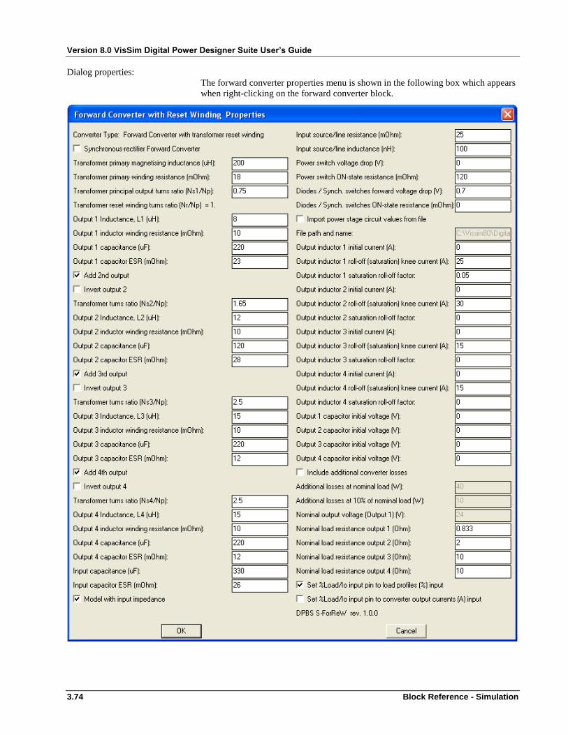
Version 8.0 VisSim Digital Power Designer Suite User’s Guide
3.74 Block Reference - Simulation
Dialog properties:
The forward converter properties menu is shown in the following box which appears
when right-clicking on the forward converter block.
Version 8.0 VisSim Digital Power Designer Suite User’s Guide
Block Reference - Simulation 3.75
Synchronous-rectifier forward Converter:
When this check box is activated the output diodes of the forward converter will be
modelled as a controllable switches (usually a MOSFET). This will activate the SWS
and SWF vector input pins.
Transformer primary magnetising inductance:
Insert the value of the forward converter transformer magnetising inductance in
micro-Henries.
Transformer primary winding resistance:
The winding resistance of the transformer primary winding should be given here in
milli-Ohms. The resistance of any connections can be summed into the given value.
Transformer principal output turns ratio (Ns1/Np):
Enter the turns ratio of the first secondary winding with respect to the primary
winding.
Transformer reset winding turns ration (Nr/Np) = 1:
Since the reset winding is clamped to the input voltage when the switch is off, the
reset winding has a fixed turns ratio of 1:1.
Output inductance L1:
Insert the value of the forward converter output 1 inductance in micro-Henries.
Output inductor internal resistance L1:
The winding resistance of the output1 inductor should be given here in milli-Ohms.
The resistance of any connections can be summed into the given value.
Output 1 capacitance:
Insert the value of the capacitor of the first or principal output in micro-Farads.
Output 1 capacitor ESR:
The equivalent series resistance (ESR) of the modelled output capacitor 1 should be
given here in milli-Ohms.
Add 2nd output:
Select this box to add a second output stage with additional transformer winding to
the forward converter.
Invert output 2:
Select this box if a negative output is required for the 2nd
output stage.
Transformer turns ratio (Ns2/Np):
Enter the turns ratio of the second output secondary winding with respect to the
primary winding.
Output inductance L2:
Insert the value of the forward converter output 2 inductance in micro-Henries.
Output inductor internal resistance L2:
The winding resistance of the output2 inductor should be given here in milli-Ohms.
The resistance of any connections can be summed into the given value.
Output 2 capacitance:
Insert the value of the capacitor of the second output in micro-Farads.
Output 2 capacitor ESR:
The equivalent series resistance (ESR) of the modelled output capacitor 2 should be
given here in milli-Ohms.
Version 8.0 VisSim Digital Power Designer Suite User’s Guide
3.76 Block Reference - Simulation
Add 3rd output:
Select this box to add a third output stage with another additional transformer
winding to the forward converter. The component values must be given similar to the
2nd
output stage above.
Add 4th output:
Select this box to add a fourth output stage with additional transformer winding to
the forward converter. The component values must be given similar to the 2nd
output
stage above.
Input capacitance:
The value of the input capacitor in micro-Farads must be given. Note that the actual
capacitance value will only affect the converter performance if “Model with input
impedance” is selected below.
Input capacitor ESR:
Insert the value of the equivalent series resistance of the input capacitor in milli-
Ohms.
Model with input impedance:
Check this box to include the input impedance in the forward converter model. This
can also be used to model the effects of an input filter in the forward converter.
Input source/line resistance:
Insert the value of the source and / or line resistance in milli-Ohms.
Input source/line inductance:
Insert the value of the source and / or line inductance in nano-Henries.
Power switch voltage drop:
The forward voltage drop, in Volts, across the main switch of the forward converter
can be entered. This value will provide a fixed forward ON-state voltage regardless
of the current flowing through the switch. This value can be combined with the ON-
state resistance below to model an IGBT switch. For a synchronous converter, if the
current through the inductor is negative and both the switches are in the OFF state,
this value will be used as the forward voltage drop of the integrated reverse diode of
the main switch.
Power switch ON-state resistance:
The ON-state resistance, in milli-Ohms, of the main switch can be entered. This
value will model a variable voltage drop dependent upon the current flowing through
the switch such as with a MOSFET.
Diodes / Synch. Switches forward voltage drop:
The forward voltage drop, in Volts, across the diodes / synchronous switches (in the
case of a synchronous-rectifier converter) and the reset winding diode of the forward
converter can be entered. This value will provide a fixed forward ON-state voltage
regardless of the current flowing through the diode. For synchronous converters, this
value is only considered when the synchronous switch is off and its reverse diode is
conducting.
Diodes / Synch. Switches ON-state resistance:
The ON-state resistance, in milli-Ohms, of the synchronous switches can be entered.
In the case of synchronous converters where the synchronous rectifier is a MOSFET
switch, the forward voltage across the diode will depend only on this value when the
switch is in the on-state (the SWS control ≥ 1), otherwise it will depend upon the
forward voltage drop only if forward biased and the switch is not controlled.
Version 8.0 VisSim Digital Power Designer Suite User’s Guide
Block Reference - Simulation 3.77
Import power stage circuit values from file:
The power component values can be directly read from a file.
File path and name:
Enter the full path and name of the file. If only the file name is inserted, it must
reside in the same directory as the main VisSim diagram.
Output inductor x initial current:
The initial inductor current (at simulation start) of each output can be entered here in
Amperes.
Output inductor x roll-off (saturation) knee current:
The converter inductor can be modelled with saturation and this is useful for
inductors constructed with soft magnetic materials. This modelling will produce an
inductor with varying inductance dependent upon the current flowing through the
inductor.
Output inductor x saturation roll-off factor:
The roll-off factor of the inductor permeability should be inserted here. For inductors
modelled without saturation, enter a value of zero here.
Output capacitor x initial voltage:
The initial voltage of the output capacitor (at simulation start) for each output can be
entered here in Volts.
Include additional converter losses:
The power converter does not model all the component losses and therefore the input
to output efficiency will be higher than expected. Since the converter duty cycle is a
function of the efficiency as:
(Forward converter in CCM)
the duty cycle will also be lower than expected. To compensate for this, additional
losses can be introduced .
Additional losses at nominal load:
Insert the required additional full-load losses in Watts.
Additional losses at 10% load:
Insert the additional losses in Watts at 10% of full-load..
Nominal output voltage, output 1:
The nominal output voltage in Volts should be entered into the box. The additional
converter losses will be constant from zero to 10% applied load and increase linearly
from 10% to the nominal (100%) applied load.
Nominal load resistance output x:
The nominal (full-load) load resistance for each output must be entered here in
Ohms.
Set %Load/Io input pin to a load profiles (%) input:
Enable this check box to vary the loads according to the values at the %Load/Io
vector input pin and the nominal load resistances.
NNs
Np
DVo
N Vi

Version 8.0 VisSim Digital Power Designer Suite User’s Guide
3.78 Block Reference - Simulation
Set %Load/Io input pin to converter output currents (A) input:
Enable this check box to vary the loads directly to the value of the current inputs in
amperes. The nominal load resistances are not considered in this case.
Flyback Converter (with RCD snubber)
The flyback converter is an isolated configuration of the buck-boost converter. The
converter can have from one to four outputs, each controlled by a single switch on
the primary side.
Input Pins: Vin Input voltage (V)
This is usually connected from a source block or it can be the output of another
converter.
SW Main switch control (SW < 1 = OFF, SW ≥ 1 = ON).
SWS(1..4) Synchronous switch control for each of the four outputs; vector rows = 1, columns =
4 (SW < 1 = OFF, SW ≥ 1 = ON).
%Load/Io[1..4] Proportion of the nominal load of each output in percent or the load currents in
amperes, depending upon the configuration of this pin in the block dialog; vector,
rows = 1, columns = 4.
This pin controls the amount of load to be applied to the converter at any time
instant. Note that one of the “Set %Load/Io input pin to…” selections must be
checked to enable this pin. The value at this pin is a percentage of the nominal load,
determined by the nominal load resistance value in the dialog (see below) or directly
the load current, depending upon the dialog selection.
Output Pins: Vout(1..4) Converter output voltages (V); vector, rows = 1, columns = 4. The voltage will be
negative if “invert output” is selected for that output.
Iout(1..4) Converter output currents (A); vector, rows = 1, columns = 4, again the output
current will be negative if “invert output” is selected for that output.
Pout(1..4) Converter output power of each output (W); vector, rows = 1, columns = 4.
Iin Converter input current (A). If “model with input impedance” is not selected within
the dialog, then this current will be the average of the input current over each
switching period. If the input capacitor is not present (Cin = 0), then this will be the
unfiltered primary winding + snubber current (when enabled) for the case of the
flyback converter. Otherwise, the current will be calculated at each simulation step
based upon the input impedance and input capacitance.
vP Voltage across the transformer primary winding (V)
iP Current flowing through the transformer primary winding (A)

Version 8.0 VisSim Digital Power Designer Suite User’s Guide
Block Reference - Simulation 3.79
Vsw Switch Voltage (V) – Positive for forward voltages.
Isw Switch Current (A) – Positive for forward current.
vS(1..4) Transformer secondary winding voltages (V); vector, rows = 1, columns = 4.
Vd(1..4) Diode Voltages of each output (V) - Positive for reverse voltages; vector, rows = 1,
columns = 4. The voltage across the flyback output diodes/ synchronous switches.
Id(1..4) Diode Currents of each output (A) – Positive for forward current; vector rows = 1,
columns = 4. The current through the flyback output diodes / synchronous switches.
This current is also the secondary winding current.
iCo(1..4) Output Capacitor Currents for each output (A) ; vector rows = 1, columns = 4.
vCin Input capacitor Voltage (V)
This will be the voltage charge on input capacitor if the “model with input
impedance” is selected, otherwise it will be directly the input voltage.
iCin Input capacitor current (A)
Sn Output (format struct) giving the various values of the RCD snubber circuit. See
below for an explanation.
%Eff Converter Efficiency (%), averaged over a switching cycle.
The value at this pin is the efficiency of the converter averaged over the last
switching cycle. The converter losses included within the model are the main switch
and diode / synchronous switch conduction losses, the inductor winding resistance
and the input and output capacitor losses due to their internal equivalent series
resistance (ESR). The dissipative loss of the RCD snubber is also included when
enabled for the flyback converter.
The switching losses and diode reverse recovery losses along with the inductor core
losses are not included in the model.
Circuit schematic: Flyback Converter

Version 8.0 VisSim Digital Power Designer Suite User’s Guide
3.80 Block Reference - Simulation
Any number from 1 to 4 separate output stages can be included in the flyback
converter model. Output stages can also be inverted for negative output voltages.
Dialog properties:
The flyback converter properties menu is shown in the following box which appears
when right-clicking on the flyback converter block.
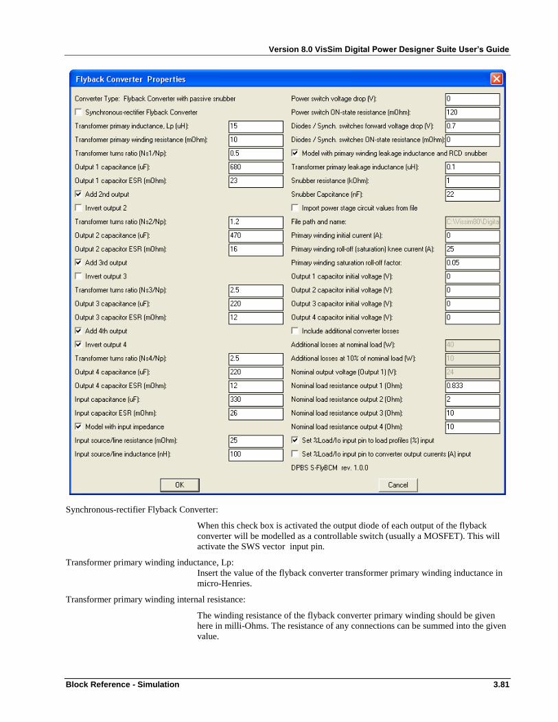
Version 8.0 VisSim Digital Power Designer Suite User’s Guide
Block Reference - Simulation 3.81
Synchronous-rectifier Flyback Converter:
When this check box is activated the output diode of each output of the flyback
converter will be modelled as a controllable switch (usually a MOSFET). This will
activate the SWS vector input pin.
Transformer primary winding inductance, Lp:
Insert the value of the flyback converter transformer primary winding inductance in
micro-Henries.
Transformer primary winding internal resistance:
The winding resistance of the flyback converter primary winding should be given
here in milli-Ohms. The resistance of any connections can be summed into the given
value.
Version 8.0 VisSim Digital Power Designer Suite User’s Guide
3.82 Block Reference - Simulation
Transformer principal output turns ratio (Ns1/Np):
Enter the turns ratio of the first secondary winding with respect to the primary
winding.
Output 1 capacitance:
Insert the value of the main output 1 capacitor in micro-Farads.
Output 1capacitor ESR:
The equivalent series resistance (ESR) of the modelled output capacitor 1 should be
given here in milli-Ohms.
Add 2nd output:
Select this box to add a second output stage with additional transformer winding to
the flybackconverter.
Invert output 2:
Select this box if a negative output is required for the 2nd
output stage.
Transformer turns ratio (Ns2/Np):
Enter the turns ratio of the second output secondary winding with respect to the
primary winding.
Output 2 capacitance:
Enter the value of the capacitor of the second output in micro-Farads.
Output 2 capacitor ESR:
The equivalent series resistance (ESR) of the modelled output capacitor 2 should be
given here in milli-Ohms.
Add 3rd output:
Select this box to add a third output stage with another additional transformer
winding to the flyback converter. The component values must be given similar to the
2nd
output stage above.
Add 4th output:
Select this box to add a fourth output stage with additional transformer winding to
the flyback converter. The component values must be given similar to the 2nd
output
stage above.
Input capacitance:
The value of the input capacitor in micro-Farads must be given. Note that the actual
capacitance value will only affect the converter performance if “Model with input
impedance” is selected below.
Input capacitor ESR:
Insert the value of the equivalent series resistance of the input capacitor in milli-
Ohms.
Model with input impedance:
Check this box to include the input impedance of the flyback converter model. This
can also be used to model the effects of an input filter in the converter.
Input source/line resistance:
Insert the value of the source and / or line resistance in milli-Ohms.
Input source/line inductance:
Insert the value of the source and / or line inductance in nano-Henries.
Power switch voltage drop:
The forward voltage drop, in Volts, across the main switch of the flyback converter
can be entered. This value will provide a fixed forward ON-state voltage regardless
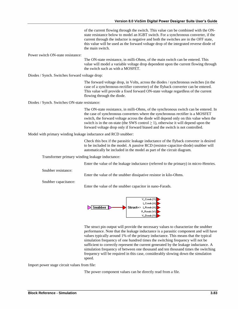
Version 8.0 VisSim Digital Power Designer Suite User’s Guide
Block Reference - Simulation 3.83
of the current flowing through the switch. This value can be combined with the ON-
state resistance below to model an IGBT switch. For a synchronous converter, if the
current through the inductor is negative and both the switches are in the OFF state,
this value will be used as the forward voltage drop of the integrated reverse diode of
the main switch.
Power switch ON-state resistance:
The ON-state resistance, in milli-Ohms, of the main switch can be entered. This
value will model a variable voltage drop dependent upon the current flowing through
the switch such as with a MOSFET.
Diodes / Synch. Switches forward voltage drop:
The forward voltage drop, in Volts, across the diodes / synchronous switches (in the
case of a synchronous-rectifier converter) of the flyback converter can be entered.
This value will provide a fixed forward ON-state voltage regardless of the current
flowing through the diode.
Diodes / Synch. Switches ON-state resistance:
The ON-state resistance, in milli-Ohms, of the synchronous switch can be entered. In
the case of synchronous converters where the synchronous rectifier is a MOSFET
switch, the forward voltage across the diode will depend only on this value when the
switch is in the on-state (the SWS control ≥ 1), otherwise it will depend upon the
forward voltage drop only if forward biased and the switch is not controlled.
Model with primary winding leakage inductance and RCD snubber:
Check this box if the parasitic leakage inductance of the flyback converter is desired
to be included in the model. A passive RCD (resistor-capacitor-diode) snubber will
automatically be included in the model as part of the circuit diagram.
Transformer primary winding leakage inductance:
Enter the value of the leakage inductance (referred to the primary) in micro-Henries.
Snubber resistance:
Enter the value of the snubber dissipative resistor in kilo-Ohms.
Snubber capacitance:
Enter the value of the snubber capacitor in nano-Farads.
The struct pin output will provide the necessary values to characterize the snubber
performance. Note that the leakage inductance is a parasitic component and will have
values typically around 1% of the primary inductance. This means that the typical
simulation frequency of one hundred times the switching frequency will not be
sufficient to correctly represent the current generated by the leakage inductance. A
simulation frequency of between one thousand and ten thousand times the switching
frequency will be required in this case, considerably slowing down the simulation
speed.
Import power stage circuit values from file:
The power component values can be directly read from a file.

Version 8.0 VisSim Digital Power Designer Suite User’s Guide
3.84 Block Reference - Simulation
File path and name:
Enter the full path and name of the file. If only the file name is inserted, it must
reside in the same directory as the main VisSim diagram.
Primary winding initial current:
The initial primary winding current (at simulation start) can be entered here in
Amperes.
Primary winding roll-off (saturation) knee current:
The converter inductor can be modelled with saturation and this is useful for
inductors constructed with soft magnetic materials. This modelling will produce an
inductor with varying inductance dependent upon the current flowing through the
inductor.
Primary winding saturation roll-off factor:
The roll-off factor of the inductor permeability should be inserted here. For inductors
modelled without saturation, enter a value of zero here.
Output capacitor x initial voltage:
The initial voltage of the output capacitor (at simulation start) of each of the four
possible outputs can be entered here in Volts.
Include additional converter losses:
The power converter does not model all the component losses and therefore the input
to output efficiency will be higher than expected. Since the converter duty cycle is a
function of the efficiency as:
(Flyback converter in CCM)
the duty cycle will also be lower than expected. To compensate for this, additional
losses can be introduced .
Additional losses at nominal load:
Insert the required additional full-load losses in Watts.
Additional losses at 10% load:
Insert the additional losses in Watts at 10% of full-load..
Nominal output voltage, output 1:
The nominal output voltage in Volts should be entered into the box. The additional
converter losses will be constant from zero to 10% applied load and increase linearly
from 10% to the nominal (100%) applied load.
Nominal load resistance output x:
The nominal (full-load) load resistance for each output must be entered here in
Ohms.
Set %Load/Io input pin to a load profiles (%) input:
Enable this check box to vary the loads according to the values at the %Load/Io
vector input pin and the nominal load resistances.
Set %Load/Io input pin to converter output currents (A) input:
Enable this check box to vary the loads directly to the value of the current inputs in
amperes. The nominal load resistances are not considered in this case.
NNs
Np
DVo
N Vi Vo
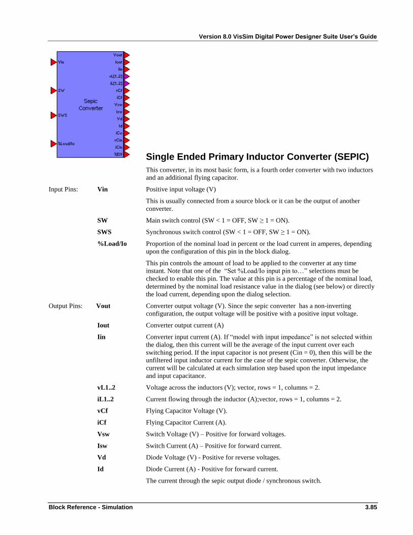
Version 8.0 VisSim Digital Power Designer Suite User’s Guide
Block Reference - Simulation 3.85
Single Ended Primary Inductor Converter (SEPIC)
This converter, in its most basic form, is a fourth order converter with two inductors
and an additional flying capacitor.
Input Pins: Vin Positive input voltage (V)
This is usually connected from a source block or it can be the output of another
converter.
SW Main switch control (SW < 1 = OFF, SW ≥ 1 = ON).
SWS Synchronous switch control (SW < 1 = OFF, SW ≥ 1 = ON).
%Load/Io Proportion of the nominal load in percent or the load current in amperes, depending
upon the configuration of this pin in the block dialog.
This pin controls the amount of load to be applied to the converter at any time
instant. Note that one of the “Set %Load/Io input pin to…” selections must be
checked to enable this pin. The value at this pin is a percentage of the nominal load,
determined by the nominal load resistance value in the dialog (see below) or directly
the load current, depending upon the dialog selection.
Output Pins: Vout Converter output voltage (V). Since the sepic converter has a non-inverting
configuration, the output voltage will be positive with a positive input voltage.
Iout Converter output current (A)
Iin Converter input current (A). If “model with input impedance” is not selected within
the dialog, then this current will be the average of the input current over each
switching period. If the input capacitor is not present (Cin = 0), then this will be the
unfiltered input inductor current for the case of the sepic converter. Otherwise, the
current will be calculated at each simulation step based upon the input impedance
and input capacitance.
vL1..2 Voltage across the inductors (V); vector, rows = 1, columns = 2.
iL1..2 Current flowing through the inductor (A);vector, rows = 1, columns = 2.
vCf Flying Capacitor Voltage (V).
iCf Flying Capacitor Current (A).
Vsw Switch Voltage (V) – Positive for forward voltages.
Isw Switch Current (A) – Positive for forward current.
Vd Diode Voltage (V) - Positive for reverse voltages.
Id Diode Current (A) - Positive for forward current.
The current through the sepic output diode / synchronous switch.
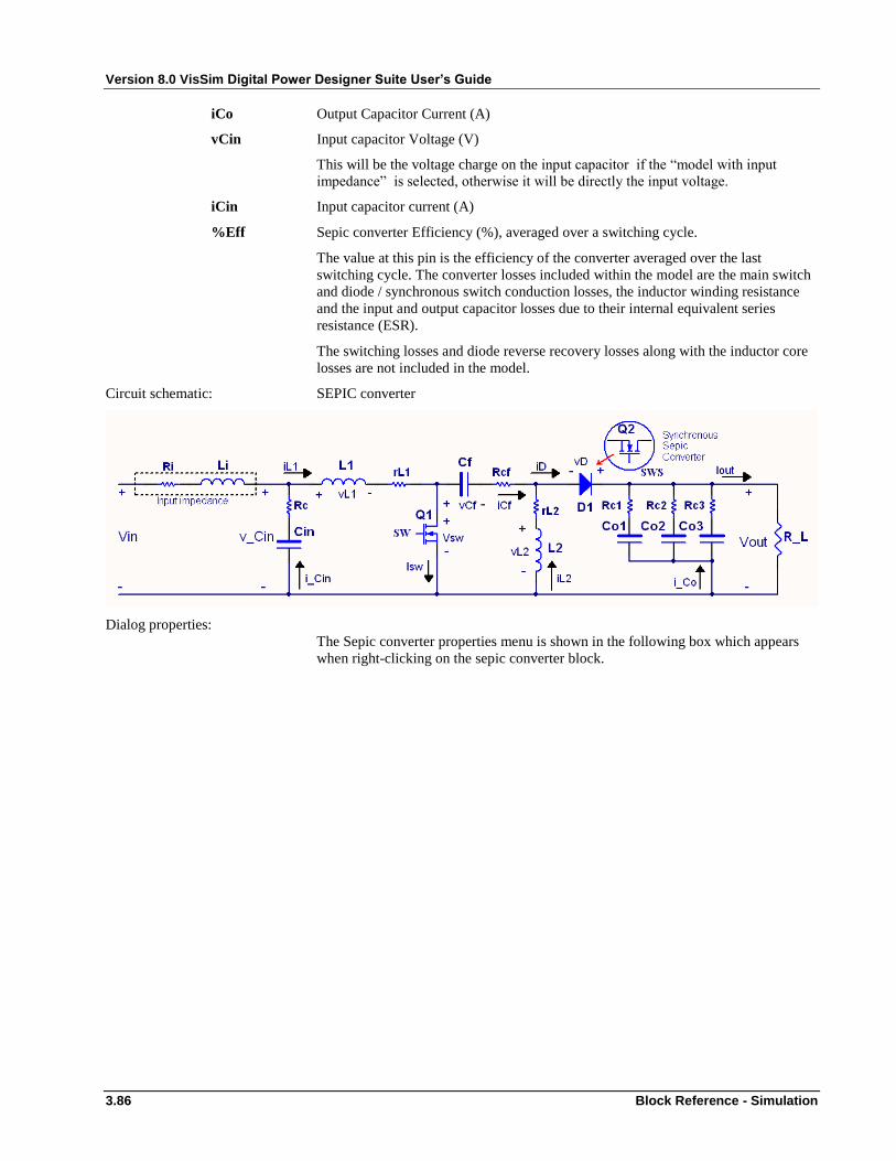
Version 8.0 VisSim Digital Power Designer Suite User’s Guide
3.86 Block Reference - Simulation
iCo Output Capacitor Current (A)
vCin Input capacitor Voltage (V)
This will be the voltage charge on the input capacitor if the “model with input
impedance” is selected, otherwise it will be directly the input voltage.
iCin Input capacitor current (A)
%Eff Sepic converter Efficiency (%), averaged over a switching cycle.
The value at this pin is the efficiency of the converter averaged over the last
switching cycle. The converter losses included within the model are the main switch
and diode / synchronous switch conduction losses, the inductor winding resistance
and the input and output capacitor losses due to their internal equivalent series
resistance (ESR).
The switching losses and diode reverse recovery losses along with the inductor core
losses are not included in the model.
Circuit schematic: SEPIC converter
Dialog properties:
The Sepic converter properties menu is shown in the following box which appears
when right-clicking on the sepic converter block.
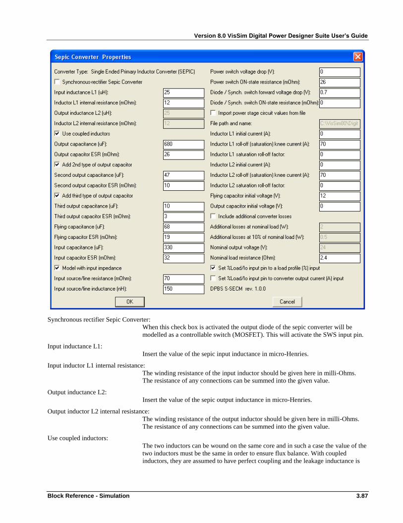
Version 8.0 VisSim Digital Power Designer Suite User’s Guide
Block Reference - Simulation 3.87
Synchronous rectifier Sepic Converter:
When this check box is activated the output diode of the sepic converter will be
modelled as a controllable switch (MOSFET). This will activate the SWS input pin.
Input inductance L1:
Insert the value of the sepic input inductance in micro-Henries.
Input inductor L1 internal resistance:
The winding resistance of the input inductor should be given here in milli-Ohms.
The resistance of any connections can be summed into the given value.
Output inductance L2:
Insert the value of the sepic output inductance in micro-Henries.
Output inductor L2 internal resistance:
The winding resistance of the output inductor should be given here in milli-Ohms.
The resistance of any connections can be summed into the given value.
Use coupled inductors:
The two inductors can be wound on the same core and in such a case the value of the
two inductors must be the same in order to ensure flux balance. With coupled
inductors, they are assumed to have perfect coupling and the leakage inductance is
Version 8.0 VisSim Digital Power Designer Suite User’s Guide
3.88 Block Reference - Simulation
neglected. The inductors will behave as having double the inductance of two single
un-coupled inductors.
Output capacitance:
Insert the value of the main output capacitor in micro-Farads.
Output capacitor ESR:
The equivalent series resistance (ESR) of the modelled output capacitor should be
given here in milli-Ohms.
Add 2nd
type of output capacitor:
An additional output capacitor (usually of a different type and a different ESR value)
which is connected in parallel with the main capacitor, can be included in the model.
Add 3rd
type of output capacitor:
A third type of output capacitor maybe included.
Flying capacitance:
The value of the input capacitor in micro-Farads must be given. Note that the actual
capacitance value will only affect the converter performance if “Model with input
impedance” is selected below.
Flying capacitor ESR:
Insert the value of the equivalent series resistance of the input capacitor in milli-
Ohms.
Input capacitance:
The value of the input capacitor in micro-Farads must be given. Note that the actual
capacitance value will only affect the converter performance if “Model with input
impedance” is selected below.
Input capacitor ESR:
Insert the value of the equivalent series resistance of the input capacitor in milli-
Ohms.
Model with input impedance:
Check this box to include the input impedance in the sepic converter model. This can
also be used to model the effects of an input filter in the converter.
Input source/line resistance:
Insert the value of the source and / or line resistance in milli-Ohms.
Input source/line inductance:
Insert the value of the source and / or line inductance in nano-Henries.
Power switches voltage drop:
The forward voltage drop, in Volts, across the main switch of the sepic converter can
be entered. This value will provide a fixed forward ON-state voltage regardless of
the current flowing through the switch. This value can be combined with the ON-
state resistance below to model an IGBT switch. For a synchronous converter, if the
current through the inductor is negative and both the switches are in the OFF state,
this value will be used as the forward voltage drop of the integrated reverse diode of
the main switch.
Power switches ON-state resistance:
The ON-state resistance, in milli-Ohms, of the main switch can be entered. This
value will model a variable voltage drop dependent upon the current flowing through
the switch such as with a MOSFET.

Version 8.0 VisSim Digital Power Designer Suite User’s Guide
Block Reference - Simulation 3.89
Diodes / Synch. Switches forward voltage drop:
The forward voltage drop, in Volts, across the diodes / synchronous switches (in the
case of a synchronous-rectifier converter) of the sepic converter can be entered. This
value will provide a fixed forward ON-state voltage regardless of the current flowing
through the diode.
Diodes / Synch. Switches ON-state resistance:
The ON-state resistance, in milli-Ohms, of the synchronous switch can be entered. In
the case of synchronous converters where the synchronous rectifier is a MOSFET
switch, the forward voltage across the diode will depend only on this value when the
switch is in the on-state (the SWS control ≥ 1), otherwise it will depend upon the
forward voltage drop only if forward biased and the switch is not controlled.
Import power stage circuit values from file:
The power component values can be directly read from a file. This file is typically
generated by the Power Stage Design Tool within the Digital Power Design Suite.
File path and name:
Enter the full path and name of the file. If only the file name is inserted, it must
reside in the same directory as the main VisSim diagram.
Inductor L1 and L2 initial current:
The initial inductor current (at simulation start) can be entered here in Amperes
separately for the inductors L1 and L2.
Inductors L1 and L2 roll-off (saturation) knee current:
The converter inductor can be modelled with saturation and this is useful for
inductors constructed with soft magnetic materials. This modelling will produce
inductors with varying inductance dependent upon the current flowing through them.
Inductors L1 and L2 saturation roll-off factor:
The roll-off factor of the inductor permeability should be inserted here. For inductors
modelled without saturation, enter a value of zero here.
Output capacitor initial voltage:
The initial voltage of the output capacitor (at simulation start) can be entered here in
Volts.
Include additional converter losses:
The power converter does not model all the component losses and therefore the input
to output efficiency will be higher than expected. Since the converter duty cycle is a
function of the efficiency as:
(Sepic converter in CCM)
the duty cycle will also be lower than expected. To compensate for this, additional
losses can be introduced .
Additional losses at nominal load:
Insert the required additional full-load losses in Watts.
Additional losses at 10% load:
Insert the additional losses in Watts at 10% of full-load..
DVo
Vi Vo

Version 8.0 VisSim Digital Power Designer Suite User’s Guide
3.90 Block Reference - Simulation
Nominal output voltage:
The nominal output voltage in Volts should be entered into the box. The additional
converter losses will be constant from zero to 10% applied load and increase linearly
from 10% to the nominal (100%) applied load.
Nominal load resistance:
The nominal (full-load) load resistance must be given here in Ohms.
Set %Load/Io input pin to a load profile (%) input:
Enable this check box to vary the load according to the value at the %Load/Io input
pin and the nominal load resistance.
Set %Load/Io input pin to converter output current (A) input:
Enable this check box to set the load directly to the value of the current input in
amperes. The nominal load resistance is not considered in this case.
Back
Ćuk Converter
The Ćuk converter, in its most basic form, is a fourth order converter with two
inductors and an additional flying capacitor. The converter is similar to the sepic
converter with the main differences being that it is an inverting converter (negative
output for a positive input) and that the input and output currents are both smoothed
with inductors.
Input Pins: Vin Positive input voltage (V)
SW Main switch control (SW < 1 = OFF, SW ≥ 1 = ON).
SWS Synchronous switch control (SW < 1 = OFF, SW ≥ 1 = ON).
%Load/Io Proportion of the nominal load in percent or the load current in amperes, depending
upon the configuration of this pin in the block dialog.
This pin controls the amount of load to be applied to the converter at any time
instant. Note that one of the “Set %Load/Io input pin to…” selections must be
checked to enable this pin. The value at this pin is a percentage of the nominal load,
determined by the nominal load resistance value in the dialog (see below) or directly
the load current, depending upon the dialog selection.
Output Pins: Vout Converter output voltage (V). Since the Ćuk converter has an inverting
configuration, the output voltage will be negative with a positive input voltage.
Iout Converter output current, again negative (A).

Version 8.0 VisSim Digital Power Designer Suite User’s Guide
Block Reference - Simulation 3.91
Iin Converter input current (A). If “model with input impedance” is not selected within
the dialog, then this current will be the average of the input current over each
switching period. If the input capacitor is not present (Cin = 0), then this will be the
unfiltered input inductor current for the case of the Ćuk converter. Otherwise, the
current will be calculated at each simulation step based upon the input impedance
and input capacitance.
vL1..2 Voltage across the inductors (V); vector, rows = 1, columns = 2.
iL1..2 Current flowing through the inductor (A); vector, rows = 1, columns = 2.
vCf Flying Capacitor Voltage (V).
iCf Flying Capacitor Current (A).
Vsw Switch Voltage (V) – Positive for forward voltages.
Isw Switch Current (A) – Positive for forward current.
Vd Diode Voltage (V) - Positive for reverse voltages.
Id Diode Current (A) - Positive for forward current.
The current through the Ćuk output diode / synchronous switch.
iCo Output Capacitor Current (A)
vCin Input capacitor Voltage (V)
This will be the voltage charge on the input capacitor if the “model with input
impedance” is selected, otherwise it will be directly the input voltage.
iCin Input capacitor current (A)
%Eff Ćuk converter Efficiency (%), averaged over a switching cycle.
Circuit schematic: Ćuk converter
Dialog properties:
The Ćuk converter properties menu is shown in the following box which appears
when right-clicking on the Ćuk converter block.
The dialog properties of the Ćuk converter are similar to the sepic converter.

Version 8.0 VisSim Digital Power Designer Suite User’s Guide
3.92 Block Reference - Simulation
Zeta Converter
This converter, in its most basic form, similar to the sepic and Cuk converters is a
fourth order converter with two inductors and an additional flying capacitor.
Input Pins: Vin Positive input voltage (V)
This is usually connected from a source block or it can be the output of another
converter.
SW Main switch control (SW < 1 = OFF, SW ≥ 1 = ON).
SWS Synchronous switch control (SW < 1 = OFF, SW ≥ 1 = ON).
%Load/Io Proportion of the nominal load in percent or the load current in amperes, depending
upon the configuration of this pin in the block dialog.
This pin controls the amount of load to be applied to the converter at any time
instant. Note that one of the “Set %Load/Io input pin to…” selections must be
checked to enable this pin. The value at this pin is a percentage of the nominal load,
determined by the nominal load resistance value in the dialog (see below) or directly
the load current, depending upon the dialog selection.
Output Pins: Vout Converter output voltage (V). Since the zeta converter has a non-inverting
configuration, the output voltage will be positive with a positive input voltage.
Iout Converter output current (A).
Iin Converter input current (A). If “model with input impedance” is not selected within
the dialog, then this current will be the average of the input current over each
switching period. If the input capacitor is not present (Cin = 0), then this will be the
unfiltered switch current for the case of the zeta converter. Otherwise, the current
will be calculated at each simulation step based upon the input impedance and input
capacitance.
vL1..2 Voltage across the inductors (V); vector, rows = 1, columns = 2.
iL1..2 Current flowing through the inductor (A);vector, rows = 1, columns = 2.
vCf Flying Capacitor Voltage (V).
iCf Flying Capacitor Current (A).
Vsw Switch Voltage (V) – Positive for forward voltages.
Isw Switch Current (A) – Positive for forward current.
Vd Diode Voltage (V) - Positive for reverse voltages.
Id Diode Current (A) - Positive for forward current.

Version 8.0 VisSim Digital Power Designer Suite User’s Guide
Block Reference - Simulation 3.93
The current through the zeta converter output diode / synchronous switch.
iCo Output Capacitor Current (A)
vCin Input capacitor Voltage (V)
This will be the voltage charge on the input capacitor if the “model with input
impedance” is selected, otherwise it will be directly the input voltage.
iCin Input capacitor current (A)
%Eff Zeta converter Efficiency (%), averaged over a switching cycle.
Circuit schematic: Zeta converter
Dialog properties:
The dialog properties of the zeta converter are similar to the sepic converter.
Push-Pull Converter (with centre-tapped secondary)
The push-pull converter is a buck-derived converter with electrical isolation between
the input and output. The push-pull converter has two controlled switches on the
centre-tapped primary side of the transformer. The centre-tapped secondary side has
two controlled switches (synchronous converter) with a split secondary winding. The
isolation is not directly represented here though the input and output voltages and
currents are represented independently from each other. It can step-up or step-down
the input voltage by appropriately setting the transformer turns ratio.
Input Pins: Vin Input voltage (V)
This is usually connected from a source block or it can be the output of another
converter.
SW[1..2] Main switches control (SW < 1 = OFF, SW ≥ 1 = ON); vector rows = 1, columns = 2
SWS[1..2] Synchronous switches control (SW < 1 = OFF, SW ≥ 1 = ON) input vector.
Version 8.0 VisSim Digital Power Designer Suite User’s Guide
3.94 Block Reference - Simulation
%Load/Io Proportion of the nominal load in percent or the load current in amperes, depending
upon the configuration of this pin in the block dialog.
This pin controls the amount of load to be applied to the converter at any time
instant. Note that one of the “Set %Load/Io input pin to…” selections must be
checked to enable this pin. The value at this pin is a percentage of the nominal load,
determined by the nominal load resistance value in the dialog (see below) or directly
the load current, depending upon the dialog selection.
Output Pins: Vout Converter output voltage (V)
Iout Converter output current (A)
Iin Converter input current (A). If “model with input impedance” is not selected within
the dialog, then this current will be the average of the input current over each
switching period. If the input capacitor is not present (Cin = 0), then this will be the
unfiltered sum of the primary winding currents for the case of the push-pull
converter. Otherwise, the current will be calculated at each simulation step based
upon the input impedance and input capacitance.
vP[1..2] Voltage across the primary winding (V); vector rows = 1, columns = 2.
iP[1..2] Current through the primary winding (A); vector rows = 1, columns = 2.
vS[1..2] Voltage across the split secondary windings (V); vector rows = 1, columns = 2.
iS[1..2] Current through the split secondary windings (A); vector rows = 1, columns = 2.
This is also the current through the output diodes / synchronous switches.
vL Voltage across the secondary side inductor (V)
iL Current flowing through the secondary side inductor (A)
Vsw[1..2] Switch Voltages (V) – Positive for forward voltages; vector rows = 1, columns = 2.
Isw[1..2] Switch Currents (A) – Positive for forward current; vector rows = 1, columns = 2.
Vd[1..2] Diode Voltages (V) - Positive for reverse voltages; vector rows = 1, columns = 2.
The voltage across the output diodes / synchronous switches.
iCo Output Capacitor Current (A)
vCin Input capacitor Voltage (V)
This will be the voltage charge on input capacitor if the “model with input
impedance” is selected, otherwise it will be directly the input voltage.
iCin Input capacitor current (A)
%Eff Converter Efficiency (%), averaged over a switching cycle.

Version 8.0 VisSim Digital Power Designer Suite User’s Guide
Block Reference - Simulation 3.95
Circuit schematic: Push-pull Converter with centre-tapped secondary
Dialog properties:
The push-pull converter properties menu is shown in the following box which
appears when right-clicking on the block.

Version 8.0 VisSim Digital Power Designer Suite User’s Guide
3.96 Block Reference - Simulation
Synchronous-rectifier center-tapped secondary:
When this check box is activated the output diodes of the center-tapped secondary
will be modelled as controllable switches (usually MOSFETs). This will activate the
SWS vector input pin.
Add DC blocking capacitor in series with the primary winding:
Check this box if a capacitor in series with the primary winding is to be included in
the model. This DC blocking capacitor is so called because it blocks the flow of DC
currents in the primary winding of the transformer, preventing saturation. This
capacitor is usually required in practise with voltage mode control. Simulations,
however, may be performed without this capacitor since saturation of the primary
winding is not modelled in the full-bridge converter block.
DC blocking capacitance:
Enter the value of the DC blocking capacitance in microfarads. Small values of
capacitance could charge up quickly, robbing voltage from the primary winding and
therefore reducing the transfer of energy capacity and increasing the duty cycle.
Large values of capacitance will mean bulky and expensive components.
DC blocking capacitor parallel resistance:
Enter the value of the resistor in parallel to the blocking capacitor in Ohms. This
resistor will allow discharging of any excessive charge on the blocking capacitor.
Transformer magnetizing inductance:
Enter the value of the transformer magnetizing inductance in milli-henries.
Transformer turns ratio (Ns1/Np = Ns2/Np):
Enter the turns ratio of the transformer N secondary divided by N primary.
Output inductance:
Enter the value of the push-pull converter output inductance in micro-Henries.
Output inductor internal resistance:
The winding resistance of the buck inductor should be given here in milli-Ohms. The
resistance of any connections can be summed into the given value.
Output capacitance:
Insert the value of the main output capacitor in micro-Farads.
Output capacitor ESR:
The equivalent series resistance (ESR) of the modelled output capacitor should be
given here in milli-Ohms.
Add 2nd
type of output capacitor:
An additional output capacitor (usually of a different type and a different ESR value)
which is connected in parallel with the main capacitor, can be included in the model.
Add 3rd
type of output capacitor:
A third type of output capacitor maybe included.
Input capacitance:
The value of the input capacitor in micro-Farads must be given. Note that the actual
capacitance value will only affect the converter performance if “Model with input
impedance” is selected below.
Input capacitor ESR:
Insert the value of the equivalent series resistance of the input capacitor in milli-
Ohms.

Version 8.0 VisSim Digital Power Designer Suite User’s Guide
Block Reference - Simulation 3.97
Model with input impedance:
Check this box to model the full-bridge converter with input impedance. This can
also be used to model the effects of an input filter on the full-bridge converter.
Input source/line resistance:
Insert the value of the source and / or line resistance in milli-Ohms.
Input source/line inductance:
Insert the value of the source and / or line inductance in nano-Henries.
Power switches voltage drop:
The forward voltage drop, in Volts, across the main switches of the push-pull
converter can be entered. This value will provide a fixed forward ON-state voltage
regardless of the current flowing through the switch. This value can be combined
with the ON-state resistance below to model an IGBT switch.
Power switches ON-state resistance:
The ON-state resistance, in milli-Ohms, of the main switch can be entered. This
value will model a variable voltage drop dependent upon the current flowing through
the switch such as with a MOSFET.
Diode / Synch. Switches forward voltage drop:
The forward voltage drop, in Volts, across the diode / synchronous switch (in the
case of a synchronous-rectifier converter) of the push-pull converter can be entered.
This value will provide a fixed forward ON-state voltage regardless of the current
flowing through the diode.
Diode / Synch. Switches ON-state resistance:
The ON-state resistance, in milli-Ohms, of the synchronous switch can be entered. In
the case of synchronous converters where the synchronous rectifier is a MOSFET
switch, the forward voltage across the diode will depend only on this value when the
switch is in the on-state (the SWS control ≥ 1), otherwise it will depend upon the
forward voltage drop only if forward biased and the switch is not controlled.
Import power stage circuit values from file:
The power component values can be directly read from a file. This file is typically
generated by the Power Stage Design Tool within the Digital Power Design Suite.
File path and name:
Enter the full path and name of the file. If only the file name is inserted, it must
reside in the same directory as the main VisSim diagram.
Initial inductor current:
The initial inductor current (at simulation start) can be entered here in Amperes.
Inductor roll-off (saturation) knee current:
The converter inductor can be modelled with saturation and this is useful for
inductors constructed with soft magnetic materials. This modelling will produce an
inductor with varying inductance dependent upon the load on the converter.
Inductor saturation roll-off factor:
The roll-off factor of the inductor permeability should be inserted here. For inductors
modelled without saturation, enter a value of zero here.
Output capacitor initial voltage:
The initial voltage of the output capacitor (at simulation start) can be entered here in
Volts.
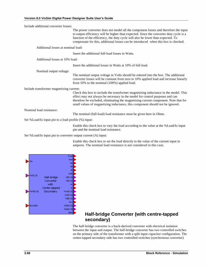
Version 8.0 VisSim Digital Power Designer Suite User’s Guide
3.98 Block Reference - Simulation
Include additional converter losses:
The power converter does not model all the component losses and therefore the input
to output efficiency will be higher than expected. Since the converter duty cycle is a
function of the efficiency, the duty cycle will also be lower than expected. To
compensate for this, additional losses can be introduced when this box is checked.
Additional losses at nominal load:
Insert the additional full-load losses in Watts.
Additional losses at 10% load:
Insert the additional losses in Watts at 10% of full-load.
Nominal output voltage:
The nominal output voltage in Volts should be entered into the box. The additional
converter losses will be constant from zero to 10% applied load and increase linearly
from 10% to the nominal (100%) applied load.
Include transformer magnetizing current:
Check this box to include the transformer magnetizing inductance in the model. This
effect may not always be necessary in the model for control purposes and can
therefore be excluded, eliminating the magnetizing current component. Note that for
small values of magnetizing inductance, this component should not be ignored.
Nominal load resistance:
The nominal (full-load) load resistance must be given here in Ohms.
Set %Load/Io input pin to a load profile (%) input:
Enable this check box to vary the load according to the value at the %Load/Io input
pin and the nominal load resistance.
Set %Load/Io input pin to converter output current (A) input:
Enable this check box to set the load directly to the value of the current input in
amperes. The nominal load resistance is not considered in this case.
Half-bridge Converter (with centre-tapped secondary)
The half-bridge converter is a buck-derived converter with electrical isolation
between the input and output. The half-bridge converter has two controlled switches
on the primary side of the transformer with a split input capacitor configuration. The
centre-tapped secondary side has two controlled switches (synchronous converter)
Version 8.0 VisSim Digital Power Designer Suite User’s Guide
Block Reference - Simulation 3.99
with a split secondary winding. The isolation is not directly represented here though
the input and output voltages and currents are represented independently from each
other. It can step-up or step-down the input voltage by appropriately setting the
transformer turns ratio.
Input Pins: Vin Input voltage (V)
This is usually connected from a source block or it can be the output of another
converter.
SW[1..2] Main switches control (SW < 1 = OFF, SW ≥ 1 = ON); vector rows = 1, columns = 2
SWS[1..2] Synchronous switches control (SW < 1 = OFF, SW ≥ 1 = ON) input vector.
%Load/Io Proportion of the nominal load in percent or the load current in amperes, depending
upon the configuration of this pin in the block dialog.
This pin controls the amount of load to be applied to the converter at any time
instant. Note that one of the “Set %Load/Io input pin to…” selections must be
checked to enable this pin. The value at this pin is a percentage of the nominal load,
determined by the nominal load resistance value in the dialog (see below) or directly
the load current, depending upon the dialog selection.
Output Pins: Vout Converter output voltage (V)
Iout Converter output current (A)
Iin Converter input current (A). If “model with input impedance” is not selected within
the dialog, then this current will be the average of the input current over each
switching period. If the input capacitor is not present (Cin = 0), then this will be the
unfiltered sum of the switch currents for the case of the half-bridge converter.
Otherwise, the current will be calculated at each simulation step based upon the input
impedance and input capacitance.
vP Voltage across the primary winding (V)
iP Current through the primary winding (A)
vCB Voltage across the DC blocking capacitor Cb (V)
vS[1..2] Voltage across the split secondary windings (V); vector rows = 1, columns = 2.
iS[1..2] Current through the split secondary windings (A); vector rows = 1, columns = 2.
This is also the current through the output diodes / synchronous switches.
vL Voltage across the secondary side inductor (V)
iL Current flowing through the secondary side inductor (A)
Vsw[1..2] Switch Voltages (V) – Positive for forward voltages; vector rows = 1, columns = 2.
Isw[1..2] Switch Currents (A) – Positive for forward current; vector rows = 1, columns = 2.
Vd[1..2] Diode Voltages (V) - Positive for reverse voltages; vector rows = 1, columns = 2.
The voltage across the output diodes / synchronous switches.
iCo Output Capacitor Current (A)
vCin Input capacitor Voltage (V)
This will be the voltage charge on input capacitor if the “model with input
impedance” is selected, otherwise it will be directly the input voltage.
iCin Input capacitor current (A)
%Eff Converter Efficiency (%), averaged over a switching cycle.
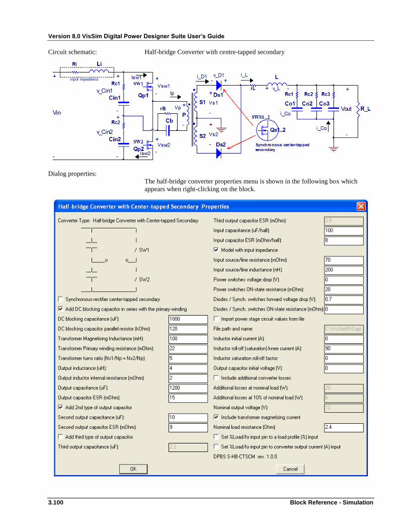
Version 8.0 VisSim Digital Power Designer Suite User’s Guide
3.100 Block Reference - Simulation
Circuit schematic: Half-bridge Converter with centre-tapped secondary
Dialog properties:
The half-bridge converter properties menu is shown in the following box which
appears when right-clicking on the block.
Version 8.0 VisSim Digital Power Designer Suite User’s Guide
Block Reference - Simulation 3.101
Synchronous-rectifier center-tapped secondary:
When this check box is activated the output diodes of the center-tapped secondary
will be modelled as controllable switches (usually MOSFETs). This will activate the
SWS vector input pin.
Add DC blocking capacitor in series with the primary winding:
Check this box if a capacitor in series with the primary winding is to be included in
the model. This DC blocking capacitor is so called because it blocks the flow of DC
currents in the primary winding of the transformer, preventing saturation. This
capacitor is usually required in practise with voltage mode control. Simulations,
however, may be performed without this capacitor since saturation of the primary
winding is not modelled in the full-bridge converter block.
DC blocking capacitance:
Enter the value of the DC blocking capacitance in microfarads. Small values of
capacitance could charge up quickly, robbing voltage from the primary winding and
therefore reducing the transfer of energy capacity and increasing the duty cycle.
Large values of capacitance will mean bulky and expensive components.
DC blocking capacitor parallel resistance:
Enter the value of the resistor in parallel to the blocking capacitor in Ohms. This
resistor will allow discharging of any excessive charge on the blocking capacitor.
Transformer magnetizing inductance:
Enter the value of the transformer magnetizing inductance in milli-henries.
Transformer turns ratio (Ns1/Np = Ns2/Np):
Enter the turns ratio of the transformer N secondary divided by N primary.
Output inductance:
Enter the value of the half-bridge converter output inductance in micro-Henries.
Output inductor internal resistance:
The winding resistance of the half-bridge output inductor should be given here in
milli-Ohms. The resistance of any connections can be summed into the given value.
Output capacitance:
Insert the value of the main output capacitor in micro-Farads.
Output capacitor ESR:
The equivalent series resistance (ESR) of the modelled output capacitor should be
given here in milli-Ohms.
Add 2nd
type of output capacitor:
An additional output capacitor (usually of a different type and a different ESR value)
which is connected in parallel with the main capacitor, can be included in the model.
Add 3rd
type of output capacitor:
A third type of output capacitor maybe included.
Input capacitance:
The value of the input capacitor in micro-Farads must be given. Note that the actual
capacitance value will only affect the converter performance if “Model with input
impedance” is selected below.
Input capacitor ESR:
Insert the value of the equivalent series resistance of the input capacitor in milli-
Ohms.
Version 8.0 VisSim Digital Power Designer Suite User’s Guide
3.102 Block Reference - Simulation
Model with input impedance:
Check this box to model the full-bridge converter with input impedance. This can
also be used to model the effects of an input filter on the full-bridge converter.
Input source/line resistance:
Insert the value of the source and / or line resistance in milli-Ohms.
Input source/line inductance:
Insert the value of the source and / or line inductance in nano-Henries.
Power switches voltage drop:
The forward voltage drop, in Volts, across the main switch of the half-bridge
converter can be entered. This value will provide a fixed forward ON-state voltage
regardless of the current flowing through the switch. This value can be combined
with the ON-state resistance below to model an IGBT switch.
Power switches ON-state resistance:
The ON-state resistance, in milli-Ohms, of the main switch can be entered. This
value will model a variable voltage drop dependent upon the current flowing through
the switch such as with a MOSFET.
Diode / Synch. Switches forward voltage drop:
The forward voltage drop, in Volts, across the diodes / synchronous switches (in the
case of a synchronous-rectifier converter) of the half-bridge converter can be
entered. This value will provide a fixed forward ON-state voltage regardless of the
current flowing through the diodes.
Diode / Synch. Switches ON-state resistance:
The ON-state resistance, in milli-Ohms, of the synchronous switch can be entered. In
the case of synchronous converters where the synchronous rectifiers are MOSFET
switches, the forward voltage across the diodes (switches) will depend only on this
value when the switch is in the on-state (the SWS control ≥ 1), otherwise it will
depend upon the forward voltage drop only if forward biased and the switch is not
controlled.
Import power stage circuit values from file:
The power component values can be directly read from a file.
File path and name:
Enter the full path and name of the file.
Initial inductor current:
The initial inductor current (at simulation start) can be entered here in Amperes.
Inductor roll-off (saturation) knee current:
The converter inductor can be modelled with saturation and this is useful for
inductors constructed with soft magnetic materials. This modelling will produce an
inductor with varying inductance dependent upon the load on the converter.
Inductor saturation roll-off factor:
The roll-off factor of the inductor permeability should be inserted here. For inductors
modelled without saturation, enter a value of zero here.
Output capacitor initial voltage:
The initial voltage of the output capacitor (at simulation start) can be entered here in
Volts.

Version 8.0 VisSim Digital Power Designer Suite User’s Guide
Block Reference - Simulation 3.103
Include additional converter losses:
The power converter does not model all the component losses and therefore the input
to output efficiency will be higher than expected. Similar to the buck converter, since
the converter duty cycle is a function of the efficiency, the duty cycle will also be
lower than expected. To compensate for this, additional losses can be introduced
when this box is checked.
Additional losses at nominal load:
Insert the additional full-load losses in Watts.
Additional losses at 10% load:
Insert the additional losses in Watts at 10% of full-load.
Nominal output voltage:
The nominal output voltage in Volts should be entered into the box. The additional
converter losses will be constant from zero to 10% applied load and increase linearly
from 10% to the nominal (100%) applied load.
Include transformer magnetizing current:
Check this box to include the transformer magnetizing inductance in the model. This
effect may not always be necessary in the model for control purposes and can
therefore be excluded, eliminating the magnetizing current component. Note that for
small values of magnetizing inductance, this component should not be ignored.
Nominal load resistance:
The nominal (full-load) load resistance must be given here in Ohms.
Set %Load/Io input pin to a load profile (%) input:
Enable this check box to vary the load according to the value at the %Load/Io input
pin and the nominal load resistance.
Set %Load/Io input pin to converter output current (A) input:
Enable this check box to set the load directly to the value of the current input in
amperes. The nominal load resistance is not considered in this case.
Full-bridge Converter (with centre-tapped secondary)
The full-bridge converter is a buck-derived converter with electrical isolation
between the input and output. The full-bridge converter has four controlled switches
on the primary side of the transformer. The centre-tapped secondary side has two

Version 8.0 VisSim Digital Power Designer Suite User’s Guide
3.104 Block Reference - Simulation
controlled switches (synchronous converter) with a split secondary winding. The
isolation is not directly represented here though the input and output voltages and
currents are represented independently from each other. It can step-up or step-down
the input voltage by appropriately setting the transformer turns ratio.
Input Pins: Vin Input voltage (V)
This is usually connected from a source block or it can be the output of another
converter.
SW(1..4) Main switches control (SW < 1 = OFF, SW ≥ 1 = ON); vector rows = 1, columns = 4
SWS(1..2) Synchronous switches control (SW < 1 = OFF, SW ≥ 1 = ON) input vector.
%Load/Io Proportion of the nominal load in percent or the load current in amperes, depending
upon the configuration of this pin in the block dialog.
This pin controls the amount of load to be applied to the converter at any time
instant. Note that one of the “Set %Load/Io input pin to…” selections must be
checked to enable this pin. The value at this pin is a percentage of the nominal load,
determined by the nominal load resistance value in the dialog (see below) or directly
the load current, depending upon the dialog selection.
Output Pins: Vout Converter output voltage (V)
Iout Converter output current (A)
Iin Converter input current (A). If “model with input impedance” is not selected within
the dialog, then this current will be the average of the input current over each
switching period. If the input capacitor is not present (Cin = 0), then this will be the
unfiltered sum of the top switch currents for the case of the full-bridge converter.
Otherwise, the current will be calculated at each simulation step based upon the input
impedance and input capacitance.
vP Voltage across the primary winding (V)
iP Current through the primary winding (A)
vCB Voltage across the DC blocking capacitor Cb (V)
vS(1..2) Voltage across the split secondary windings (V); vector rows = 1, columns = 2.
iS(1..2) Current through the split secondary windings (A); vector rows = 1, columns = 2.
This is also the current through the output diodes / synchronous switches.
vL Voltage across the secondary side inductor (V)
iL Current flowing through the secondary side inductor (A)
Vsw(1..4) Switch Voltages (V) – Positive for forward voltages; vector rows = 1, columns = 4.
Isw(1..4) Switch Currents (A) – Positive for forward current; vector rows = 1, columns = 4.
Vd(1..2) Diode Voltages (V) - Positive for reverse voltages; vector rows = 1, columns = 2.
The voltage across the output diodes / synchronous switches.
iCo Output Capacitor Current (A)
vCin Input capacitor Voltage (V)
This will be the voltage charge on input capacitor if the “model with input
impedance” is selected, otherwise it will be directly the input voltage.
iCin Input capacitor current (A)
%Eff Converter Efficiency (%), averaged over a switching cycle.
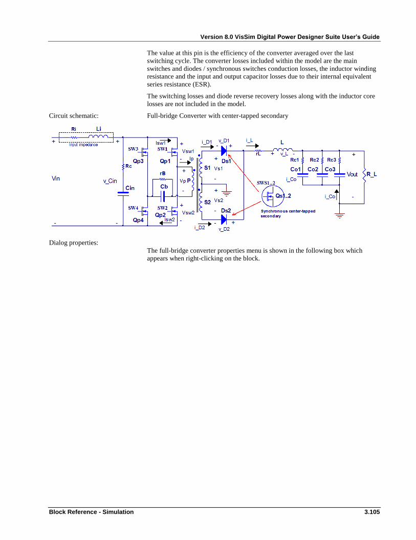
Version 8.0 VisSim Digital Power Designer Suite User’s Guide
Block Reference - Simulation 3.105
The value at this pin is the efficiency of the converter averaged over the last
switching cycle. The converter losses included within the model are the main
switches and diodes / synchronous switches conduction losses, the inductor winding
resistance and the input and output capacitor losses due to their internal equivalent
series resistance (ESR).
The switching losses and diode reverse recovery losses along with the inductor core
losses are not included in the model.
Circuit schematic: Full-bridge Converter with center-tapped secondary
Dialog properties:
The full-bridge converter properties menu is shown in the following box which
appears when right-clicking on the block.
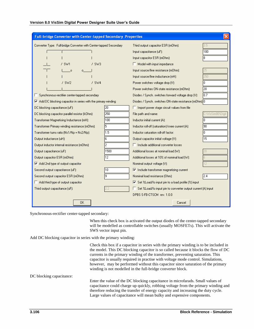
Version 8.0 VisSim Digital Power Designer Suite User’s Guide
3.106 Block Reference - Simulation
Synchronous-rectifier center-tapped secondary:
When this check box is activated the output diodes of the center-tapped secondary
will be modelled as controllable switches (usually MOSFETs). This will activate the
SWS vector input pin.
Add DC blocking capacitor in series with the primary winding:
Check this box if a capacitor in series with the primary winding is to be included in
the model. This DC blocking capacitor is so called because it blocks the flow of DC
currents in the primary winding of the transformer, preventing saturation. This
capacitor is usually required in practise with voltage mode control. Simulations,
however, may be performed without this capacitor since saturation of the primary
winding is not modelled in the full-bridge converter block.
DC blocking capacitance:
Enter the value of the DC blocking capacitance in microfarads. Small values of
capacitance could charge up quickly, robbing voltage from the primary winding and
therefore reducing the transfer of energy capacity and increasing the duty cycle.
Large values of capacitance will mean bulky and expensive components.
Version 8.0 VisSim Digital Power Designer Suite User’s Guide
Block Reference - Simulation 3.107
DC blocking capacitor parallel resistance:
Enter the value of the resistor in parallel to the blocking capacitor in Ohms. This
resistor will allow discharging of any excessive charge on the blocking capacitor.
Transformer magnetizing inductance:
Enter the value of the transformer magnetizing inductance in milli-henries.
Transformer turns ratio (Ns1/Np = Ns2/Np):
Enter the turns ratio of the transformer N secondary divided by N primary.
Output inductance:
Enter the value of the full-bridge converter output inductance in micro-Henries.
Output inductor internal resistance:
The winding resistance of the full-bridge output inductor should be given here in
milli-Ohms. The resistance of any connections can be summed into the given value.
Output capacitance:
Insert the value of the main output capacitor in micro-Farads.
Output capacitor ESR:
The equivalent series resistance (ESR) of the modelled output capacitor should be
given here in milli-Ohms.
Add 2nd
type of output capacitor:
An additional output capacitor (usually of a different type and a different ESR value)
which is connected in parallel with the main capacitor, can be included in the model.
Add 3rd
type of output capacitor:
A third type of output capacitor maybe included.
Input capacitance:
The value of the input capacitor in micro-Farads must be given. Note that the actual
capacitance value will only affect the converter performance if “Model with input
impedance” is selected below.
Input capacitor ESR:
Insert the value of the equivalent series resistance of the input capacitor in milli-
Ohms.
Model with input impedance:
Check this box to model the full-bridge converter with input impedance. This can
also be used to model the effects of an input filter on the full-bridge converter.
Input source/line resistance:
Insert the value of the source and / or line resistance in milli-Ohms.
Input source/line inductance:
Insert the value of the source and / or line inductance in nano-Henries.
Power switch voltage drop:
The forward voltage drop, in Volts, across the main switches of the full-bridge
converter can be entered. This value will provide a fixed forward ON-state voltage
regardless of the current flowing through the switch. This value can be combined
with the ON-state resistance below to model an IGBT switch.
Power switch ON-state resistance:
The ON-state resistance, in milli-Ohms, of the main switch can be entered. This
value will model a variable voltage drop dependent upon the current flowing through
the switch such as with a MOSFET.

Version 8.0 VisSim Digital Power Designer Suite User’s Guide
3.108 Block Reference - Simulation
Diode / Synch. Switch forward voltage drop:
The forward voltage drop, in Volts, across the diodes / synchronous switches (in the
case of a synchronous-rectifier converter) of the full-bridge converter can be entered.
This value will provide a fixed forward ON-state voltage regardless of the current
flowing through the diode.
Diode / Synch. Switch ON-state resistance:
The ON-state resistance, in milli-Ohms, of the synchronous switch can be entered. In
the case of synchronous converters where the synchronous rectifiers are MOSFET
switches, the forward voltage across the diodes (switches) will depend only on this
value when the switches are in the on-state (the SWS control ≥ 1), otherwise it will
depend upon the forward voltage drop only if forward biased and the switches are
not controlled.
Import power stage circuit values from file:
The power component values can be directly read from a file.
File path and name:
Enter the full path and name of the file. If only the file name is inserted, it must
reside in the same directory as the main VisSim diagram.
Initial inductor current:
The initial inductor current (at simulation start) can be entered here in Amperes.
Inductor roll-off (saturation) knee current:
The converter inductor can be modelled with saturation and this is useful for
inductors constructed with soft magnetic materials. This modelling will produce an
inductor with varying inductance dependent upon the load on the converter.
Inductor saturation roll-off factor:
The roll-off factor of the inductor permeability should be inserted here. For inductors
modelled without saturation, enter a value of zero here.
Output capacitor initial voltage:
The initial voltage of the output capacitor (at simulation start) can be entered here in
Volts.
Include additional converter losses:
The power converter does not model all the component losses and therefore the input
to output efficiency will be higher than expected. Similar to the forward converter,
since the converter duty cycle is a function of the efficiency, the duty cycle will also
be lower than expected. To compensate for this, additional losses can be introduced
when this box is checked.
Additional losses at nominal load:
Insert the additional full-load losses in Watts.
Additional losses at 10% load:
Insert the additional losses in Watts at 10% of full-load.
Nominal output voltage:
The nominal output voltage in Volts should be entered into the box. The additional
converter losses will be constant from zero to 10% applied load and increase linearly
from 10% to the nominal (100%) applied load.
Include transformer magnetizing current:
Check this box to include the transformer magnetizing inductance in the model. This
effect may not always be necessary in the model for control purposes and can

Version 8.0 VisSim Digital Power Designer Suite User’s Guide
Block Reference - Simulation 3.109
therefore be excluded, eliminating the magnetizing current component. Note that for
small values of magnetizing inductance, this component should not be ignored.
Nominal load resistance:
The nominal (full-load) load resistance must be given here in Ohms.
Set %Load/Io input pin to a load profile (%) input:
Enable this check box to vary the load according to the value at the %Load/Io input
pin and the nominal load resistance.
Set %Load/Io input pin to converter output current (A) input:
Enable this check box to set the load directly to the value of the current input in
amperes. The nominal load resistance is not considered in this case.
Back
Full-bridge Converter (with current-doubler secondary)
The full-bridge converter is a buck-derived converter with electrical isolation
between the input and output. This full-bridge converter has four controlled switches
on the primary side of the transformer and four uncontrolled diode switches on the
secondary side of the transformer. The transformer of this converter has a single
secondary winding. This secondary configuration has 2 inductors and could have
applications for high currents at lower output voltages. This converter is included as
a comparison only to the center-tapped and full-bridge secondary configurations of
the full-bridge converter.
Input Pins: Vin Input voltage (V)
SW(1..4) Main switches control (SW < 1 = OFF, SW ≥ 1 = ON); vector rows = 1, columns = 4
SWS(1..2) Synchronous switches control (SW < 1 = OFF, SW ≥ 1 = ON); vector rows = 1,
columns = 2.
%Load/Io Proportion of the nominal load in percent or the load current in amperes, depending
upon the configuration of this pin in the block dialog.
This pin controls the amount of load to be applied to the converter at any time
instant. Note that one of the “Set %Load/Io input pin to…” selections must be

Version 8.0 VisSim Digital Power Designer Suite User’s Guide
3.110 Block Reference - Simulation
checked to enable this pin. The value at this pin is a percentage of the nominal load,
determined by the nominal load resistance value in the dialog (see below) or directly
the load current, depending upon the dialog selection.
Output Pins: Vout Converter output voltage (V).
Iout Converter output current (A).
Iin Converter input current (A). If “model with input impedance” is not selected within
the dialog, then this current will be the average of the input current over each
switching period. If the input capacitor is not present (Cin = 0), then this will be the
unfiltered sum of the top switch currents for the case of the full-bridge converter.
Otherwise, the current will be calculated at each simulation step based upon the input
impedance and input capacitance.
vP Voltage across the primary winding (V)
iP Current through the primary winding (A)
vCB Voltage across the DC blocking capacitor Cb (V)
vS Voltage across the secondary winding (V).
iS Current through the secondary winding (A).
vL(1..2) Voltage across the secondary side inductors (V); vector, rows = 1, columns = 2.
iL(1..2) Current flowing through the secondary side inductors (A); vector, rows = 1, columns
= 2.
Vsw(1..4) Switch Voltages (V) – Positive for forward voltages; vector rows = 1, columns = 4.
Isw(1..4) Switch Currents (A) – Positive for forward current; vector rows = 1, columns = 4.
Vd(1..2) Diode / Sync switch Voltages (V) - Positive for reverse voltages; vector rows = 1,
columns = 2.
Id(1..2) Diode / synch switch currents (A) - Positive for forward currents; vector rows = 1,
columns = 2.
iCo Output Capacitor Current (A)
vCin Input capacitor Voltage (V)
This will be the voltage charge on input capacitor if the “model with input
impedance” is selected, otherwise it will be directly the input voltage.
iCin Input capacitor current (A)
%Eff Converter Efficiency (%), averaged over a switching cycle.
Dialog properties:
The dialog and features are similar to the full-bridge converter with centre-tapped
secondary.
Circuit schematic: Full-bridge Converter with current-doubler secondary
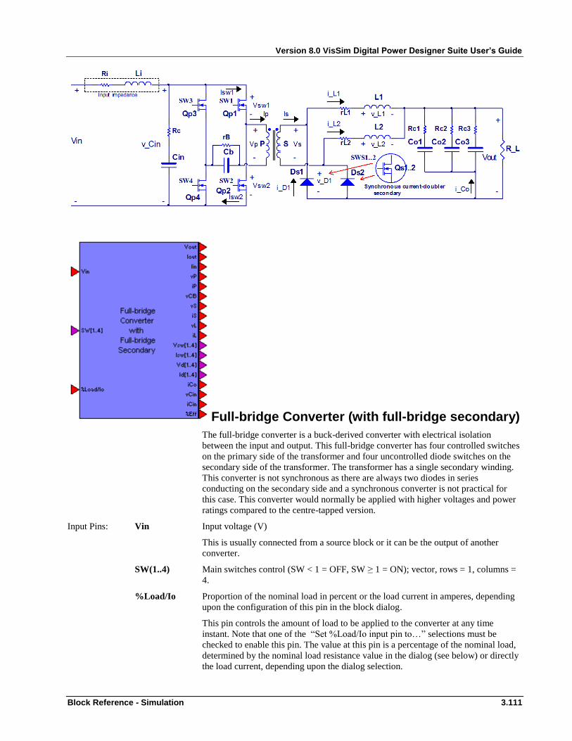
Version 8.0 VisSim Digital Power Designer Suite User’s Guide
Block Reference - Simulation 3.111
Full-bridge Converter (with full-bridge secondary)
The full-bridge converter is a buck-derived converter with electrical isolation
between the input and output. This full-bridge converter has four controlled switches
on the primary side of the transformer and four uncontrolled diode switches on the
secondary side of the transformer. The transformer has a single secondary winding.
This converter is not synchronous as there are always two diodes in series
conducting on the secondary side and a synchronous converter is not practical for
this case. This converter would normally be applied with higher voltages and power
ratings compared to the centre-tapped version.
Input Pins: Vin Input voltage (V)
This is usually connected from a source block or it can be the output of another
converter.
SW(1..4) Main switches control (SW < 1 = OFF, SW ≥ 1 = ON); vector, rows = 1, columns =
4.
%Load/Io Proportion of the nominal load in percent or the load current in amperes, depending
upon the configuration of this pin in the block dialog.
This pin controls the amount of load to be applied to the converter at any time
instant. Note that one of the “Set %Load/Io input pin to…” selections must be
checked to enable this pin. The value at this pin is a percentage of the nominal load,
determined by the nominal load resistance value in the dialog (see below) or directly
the load current, depending upon the dialog selection.
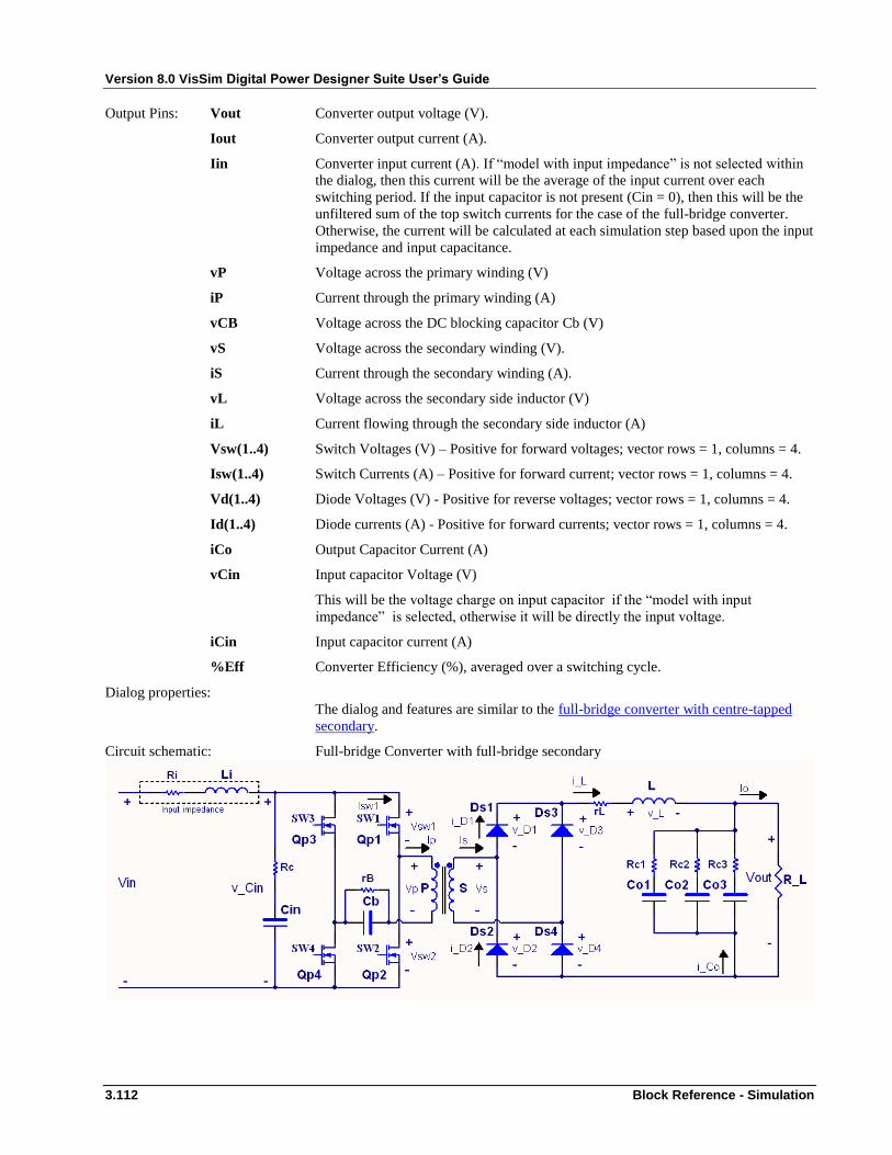
Version 8.0 VisSim Digital Power Designer Suite User’s Guide
3.112 Block Reference - Simulation
Output Pins: Vout Converter output voltage (V).
Iout Converter output current (A).
Iin Converter input current (A). If “model with input impedance” is not selected within
the dialog, then this current will be the average of the input current over each
switching period. If the input capacitor is not present (Cin = 0), then this will be the
unfiltered sum of the top switch currents for the case of the full-bridge converter.
Otherwise, the current will be calculated at each simulation step based upon the input
impedance and input capacitance.
vP Voltage across the primary winding (V)
iP Current through the primary winding (A)
vCB Voltage across the DC blocking capacitor Cb (V)
vS Voltage across the secondary winding (V).
iS Current through the secondary winding (A).
vL Voltage across the secondary side inductor (V)
iL Current flowing through the secondary side inductor (A)
Vsw(1..4) Switch Voltages (V) – Positive for forward voltages; vector rows = 1, columns = 4.
Isw(1..4) Switch Currents (A) – Positive for forward current; vector rows = 1, columns = 4.
Vd(1..4) Diode Voltages (V) - Positive for reverse voltages; vector rows = 1, columns = 4.
Id(1..4) Diode currents (A) - Positive for forward currents; vector rows = 1, columns = 4.
iCo Output Capacitor Current (A)
vCin Input capacitor Voltage (V)
This will be the voltage charge on input capacitor if the “model with input
impedance” is selected, otherwise it will be directly the input voltage.
iCin Input capacitor current (A)
%Eff Converter Efficiency (%), averaged over a switching cycle.
Dialog properties:
The dialog and features are similar to the full-bridge converter with centre-tapped
secondary.
Circuit schematic: Full-bridge Converter with full-bridge secondary
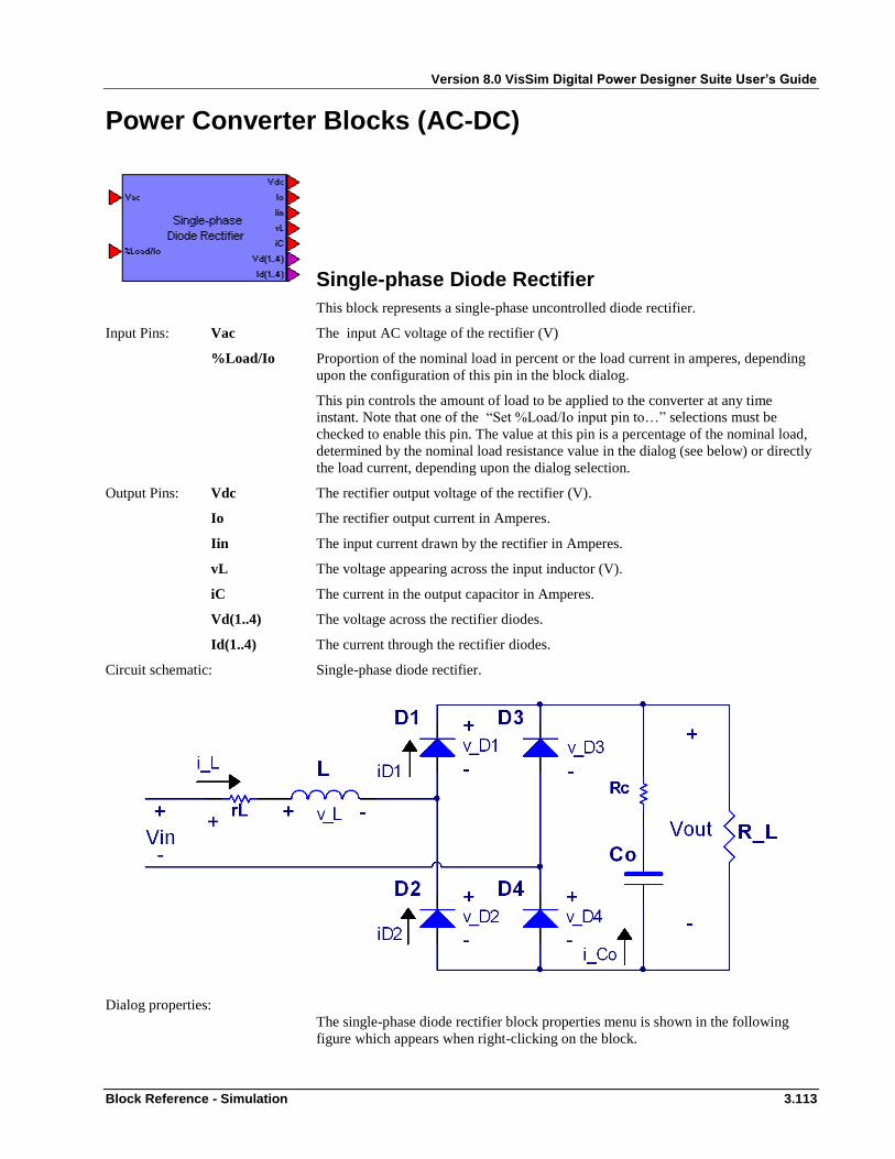
Version 8.0 VisSim Digital Power Designer Suite User’s Guide
Block Reference - Simulation 3.113
Power Converter Blocks (AC-DC)
Single-phase Diode Rectifier
This block represents a single-phase uncontrolled diode rectifier.
Input Pins: Vac The input AC voltage of the rectifier (V)
%Load/Io Proportion of the nominal load in percent or the load current in amperes, depending
upon the configuration of this pin in the block dialog.
This pin controls the amount of load to be applied to the converter at any time
instant. Note that one of the “Set %Load/Io input pin to…” selections must be
checked to enable this pin. The value at this pin is a percentage of the nominal load,
determined by the nominal load resistance value in the dialog (see below) or directly
the load current, depending upon the dialog selection.
Output Pins: Vdc The rectifier output voltage of the rectifier (V).
Io The rectifier output current in Amperes.
Iin The input current drawn by the rectifier in Amperes.
vL The voltage appearing across the input inductor (V).
iC The current in the output capacitor in Amperes.
Vd(1..4) The voltage across the rectifier diodes.
Id(1..4) The current through the rectifier diodes.
Circuit schematic: Single-phase diode rectifier.
Dialog properties:
The single-phase diode rectifier block properties menu is shown in the following
figure which appears when right-clicking on the block.
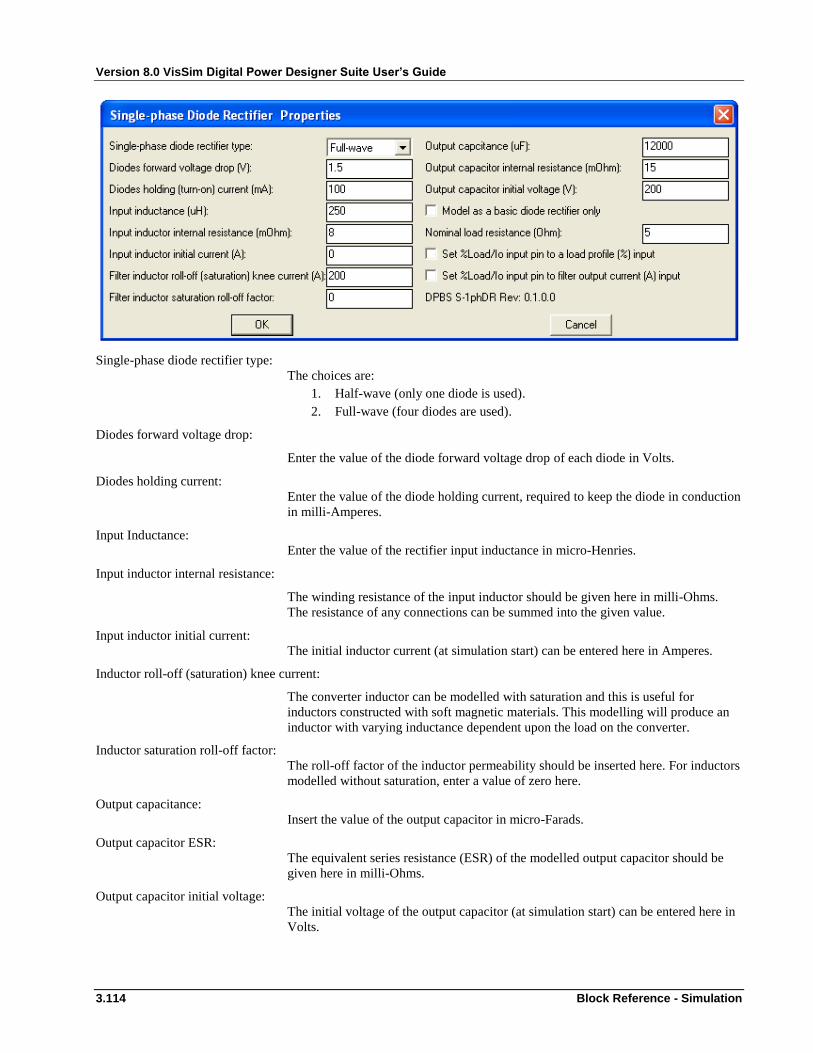
Version 8.0 VisSim Digital Power Designer Suite User’s Guide
3.114 Block Reference - Simulation
Single-phase diode rectifier type:
The choices are:
1. Half-wave (only one diode is used).
2. Full-wave (four diodes are used).
Diodes forward voltage drop:
Enter the value of the diode forward voltage drop of each diode in Volts.
Diodes holding current:
Enter the value of the diode holding current, required to keep the diode in conduction
in milli-Amperes.
Input Inductance:
Enter the value of the rectifier input inductance in micro-Henries.
Input inductor internal resistance:
The winding resistance of the input inductor should be given here in milli-Ohms.
The resistance of any connections can be summed into the given value.
Input inductor initial current:
The initial inductor current (at simulation start) can be entered here in Amperes.
Inductor roll-off (saturation) knee current:
The converter inductor can be modelled with saturation and this is useful for
inductors constructed with soft magnetic materials. This modelling will produce an
inductor with varying inductance dependent upon the load on the converter.
Inductor saturation roll-off factor:
The roll-off factor of the inductor permeability should be inserted here. For inductors
modelled without saturation, enter a value of zero here.
Output capacitance:
Insert the value of the output capacitor in micro-Farads.
Output capacitor ESR:
The equivalent series resistance (ESR) of the modelled output capacitor should be
given here in milli-Ohms.
Output capacitor initial voltage:
The initial voltage of the output capacitor (at simulation start) can be entered here in
Volts.
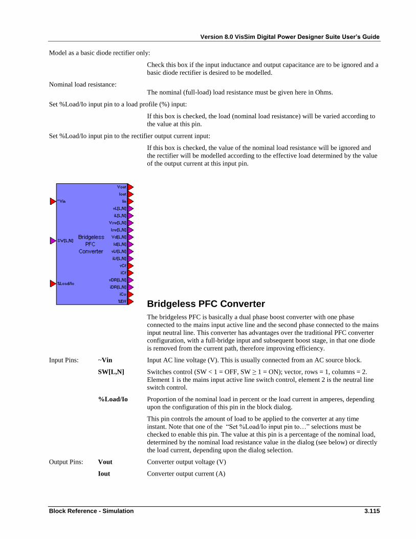
Version 8.0 VisSim Digital Power Designer Suite User’s Guide
Block Reference - Simulation 3.115
Model as a basic diode rectifier only:
Check this box if the input inductance and output capacitance are to be ignored and a
basic diode rectifier is desired to be modelled.
Nominal load resistance:
The nominal (full-load) load resistance must be given here in Ohms.
Set %Load/Io input pin to a load profile (%) input:
If this box is checked, the load (nominal load resistance) will be varied according to
the value at this pin.
Set %Load/Io input pin to the rectifier output current input:
If this box is checked, the value of the nominal load resistance will be ignored and
the rectifier will be modelled according to the effective load determined by the value
of the output current at this input pin.
Bridgeless PFC Converter
The bridgeless PFC is basically a dual phase boost converter with one phase
connected to the mains input active line and the second phase connected to the mains
input neutral line. This converter has advantages over the traditional PFC converter
configuration, with a full-bridge input and subsequent boost stage, in that one diode
is removed from the current path, therefore improving efficiency.
Input Pins: ~Vin Input AC line voltage (V). This is usually connected from an AC source block.
SW[L,N] Switches control (SW < 1 = OFF, SW ≥ 1 = ON); vector, rows = 1, columns = 2.
Element 1 is the mains input active line switch control, element 2 is the neutral line
switch control.
%Load/Io Proportion of the nominal load in percent or the load current in amperes, depending
upon the configuration of this pin in the block dialog.
This pin controls the amount of load to be applied to the converter at any time
instant. Note that one of the “Set %Load/Io input pin to…” selections must be
checked to enable this pin. The value at this pin is a percentage of the nominal load,
determined by the nominal load resistance value in the dialog (see below) or directly
the load current, depending upon the dialog selection.
Output Pins: Vout Converter output voltage (V)
Iout Converter output current (A)

Version 8.0 VisSim Digital Power Designer Suite User’s Guide
3.116 Block Reference - Simulation
Iin Converter input current (A). If “include input filter” is not selected within the dialog,
then this current will be the average of the input current over each switching period.
If the input capacitor is not present (Cin = 0), then this will be the unfiltered sum of
the inductor currents. Otherwise, the current will be calculated at each simulation
step based upon the filter inductance and capacitance.
vL[L,N] Voltages across the input boost inductors (V)
iL[L,N] Current through the input boost inductors (A).
Vsw[L,N] Switch voltages (V) – Positive for forward voltages; vector, rows = 1, columns = 2.
Isw[L,N] Switch currents (A) – Positive for forward current; vector, rows = 1, columns = 2.
Vd[L,N] Diode voltages (V) - Positive for reverse voltages; vector, rows = 1, columns = 2.
Id[L,N] Current through the output diodes; vector rows = 1, columns = 2. This is also the
current through the split secondary windings.
vLf[L,N] Voltages across the input filter inductors (V)
iLf[L,N] Current through the input filter inductors (A).
vCf Input filter capacitor Voltage (V).
This will be the voltage charge on input capacitor if the “include input filter” is
selected, otherwise it will be directly the input voltage.
iCf Input filter capacitor current (A).
vDR[L,N] Voltage across the input return diodes in volts (when “Include input return diodes” is
selected in the dialog).
iDR[L,N] Current through the input return path diodes (A).
iCo Output Capacitor Current (A)
%Eff Converter Efficiency (%), averaged over a switching cycle.
Circuit schematic: Bridgeless PFC Converter.
Dialog properties:
The bridgeless PFC converter properties menu is shown in the following box which
appears when right-clicking on the block.
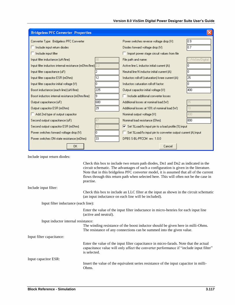
Version 8.0 VisSim Digital Power Designer Suite User’s Guide
Block Reference - Simulation 3.117
Include input return diodes:
Check this box to include two return path diodes, Dn1 and Dn2 as indicated in the
circuit schematic. The advantages of such a configuration is given in the literature.
Note that in this bridgeless PFC converter model, it is assumed that all of the current
flows through this return path when selected here. This will often not be the case in
practise.
Include input filter:
Check this box to include an LLC filter at the input as shown in the circuit schematic
(an input inductance on each line will be included).
Input filter inductance (each line):
Enter the value of the input filter inductance in micro-henries for each input line
(active and neutral).
Input inductor internal resistance:
The winding resistance of the boost inductor should be given here in milli-Ohms.
The resistance of any connections can be summed into the given value.
Input filter capacitance:
Enter the value of the input filter capacitance in micro-farads. Note that the actual
capacitance value will only affect the converter performance if “include input filter”
is selected.
Input capacitor ESR:
Insert the value of the equivalent series resistance of the input capacitor in milli-
Ohms.

Version 8.0 VisSim Digital Power Designer Suite User’s Guide
3.118 Block Reference - Simulation
Boost inductance (each line):
Enter the value of the input boost inductance of each input line in micro-henries.
Boost inductors internal resistance:
Insert the value of the equivalent series resistance of each boost inductor in milli-
Ohms.
Output capacitance:
Insert the value of the main output capacitor in micro-Farads.
Output capacitor ESR:
The equivalent series resistance (ESR) of the modelled output capacitor should be
given here in milli-Ohms.
Add 2nd
type of output capacitor:
An additional output capacitor (usually of a different type and a different ESR value)
which is connected in parallel with the main capacitor, can be included in the model.
Power switches forward voltage drop:
The forward voltage drop, in Volts, across the main switches can be entered. This
value will provide a fixed forward ON-state voltage regardless of the current flowing
through the switch.
Power switches ON-state resistance:
The ON-state resistance, in milli-Ohms, of the main switches can be entered. This
value will model a variable voltage drop dependent upon the current flowing through
the switch such as with a MOSFET.
Power switches reverse voltage drop:
The reverse voltage drop, in Volts, across the main switches can be entered. This
value will model the voltage drop across the reverse diode of the power switches.
Diodes forward voltage drop:
The forward voltage drop, in Volts, across the diodes of the bridgeless PFC converter
can be entered. This value will provide a fixed forward ON-state voltage regardless
of the current flowing through the diode. This voltage drop also applies to the input
return diodes (when this configuration is selected).
Import power stage circuit values from file:
The power component values can be directly read from a file. This file is typically
generated by the Power Stage Design Tool within the Digital Power Design Suite.
File path and name:
Enter the full path and name of the file. If only the file name is inserted, it must
reside in the same directory as the main VisSim diagram.
Active line L initial inductor current:
The initial inductor current for the active line (at simulation start) can be entered here
in Amperes.
Neutral line N initial inductor current:
The initial inductor current for the neutral line (at simulation start) can be entered
here in Amperes.
Inductor roll-off (saturation) knee current:
The converter inductor can be modelled with saturation and this is useful for
inductors constructed with soft magnetic materials. This modelling will produce an
inductor with varying inductance dependent upon the load on the converter.

Version 8.0 VisSim Digital Power Designer Suite User’s Guide
Block Reference - Simulation 3.119
Inductor saturation roll-off factor:
The roll-off factor of the inductor permeability should be inserted here. For inductors
modelled without saturation, enter a value of zero here.
Output capacitor initial voltage:
The initial voltage of the output capacitor (at simulation start) can be entered here in
Volts.
Include additional converter losses:
Similarly to the boost converter, the power converter does not model all the
component losses and therefore the input to output efficiency will be higher than
expected.
Additional losses at nominal load:
Insert the required additional full-load losses in Watts.
Additional losses at 10% load:
Insert the additional losses in Watts at 10% of full-load..
Nominal output voltage:
The nominal output voltage in Volts should be entered into the box. The additional
converter losses will be constant from zero to 10% applied load and increase linearly
from 10% to the nominal (100%) applied load.
Nominal load resistance:
The nominal (full-load) load resistance must be given here in Ohms.
Set %Load/Io input pin to a load profile (%) input:
Enable this check box to vary the load according to the value at the %Load/Io input
pin and the nominal load resistance.
Set %Load/Io input pin to converter output current (A) input:
Enable this check box to set the load directly to the value of the current input in
amperes. The nominal load resistance is not considered in this case.

Version 8.0 VisSim Digital Power Designer Suite User’s Guide
3.120 Block Reference - Simulation
Controllers
Controllers implement a particular control technique to achieve the desired converter
regulation. They are used together with one or more compensator blocks.
Voltage mode controller (VMC)
Input Pins: ON/OFF\ Enable pin (ON ≥ 1, OFF < 1) of the voltage mode controller.
Vcorr Input pin usually from the output of a compensator.
Vin Input voltage measurement pin. This measurement is used for feed-forward
compensation in VMC.
Vo Output voltage measurement pin. This measurement is only used for feed-forward
compensation with the boost and buck-boost configurations.
CL (=1) Current limit trigger input. A value ≥ 1 activates the current limit, switching off the
output PWM to be reset on the next switching cycle – a cycle-by-cycle (CBC)
current limit.
Vref% The input to this pin (in percent) will vary the internally set Vref voltage (only active
if “Use Vref profile” is checked.
Output pins: PWM1 The pulse-width modulated (PWM) output which can be connected to a power
converter SW input.
PWM2 A second pulse-width modulated (PWM) output which can be connected to a power
converter SW input for converters with two control switches such as the half-bridge,
full-bridge and push-pull converters. Note that this pin is only active when the
“Alternating PWM controller” option is checked. The PWM outputs will then be
alternated and modulated 180° out of phase.
Ramp The internal control ramp at the PWM frequency.
mod The internal modulation which along with the ramp determines the duty cycle of the
PWM output.
Vset This is the set point voltage sent out to this pin. This voltage will normally be the
internal Vref voltage however it will vary during soft start.
ENcomp This is an enable output which is typically connected to a compensator block. This
pin can disable the compensator during current limit for example.
Dialog properties:
The voltage mode controller block properties menu is shown in the following box
which appears when right-clicking on the block.
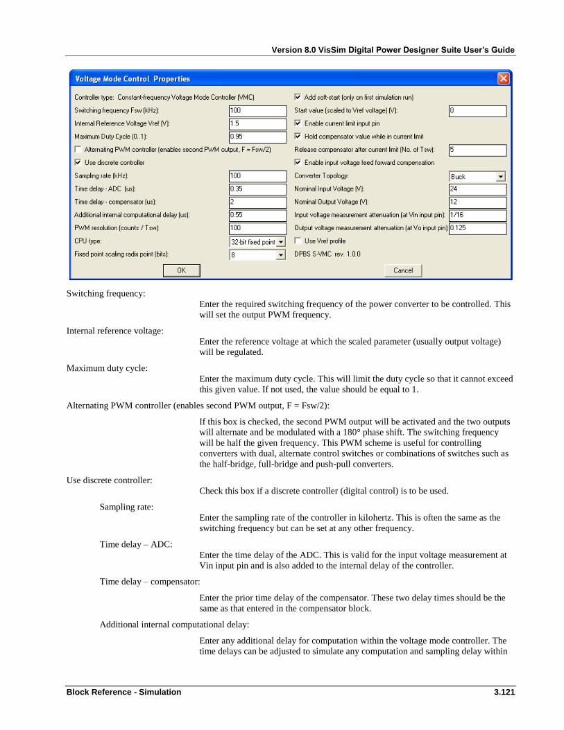
Version 8.0 VisSim Digital Power Designer Suite User’s Guide
Block Reference - Simulation 3.121
Switching frequency:
Enter the required switching frequency of the power converter to be controlled. This
will set the output PWM frequency.
Internal reference voltage:
Enter the reference voltage at which the scaled parameter (usually output voltage)
will be regulated.
Maximum duty cycle:
Enter the maximum duty cycle. This will limit the duty cycle so that it cannot exceed
this given value. If not used, the value should be equal to 1.
Alternating PWM controller (enables second PWM output, F = Fsw/2):
If this box is checked, the second PWM output will be activated and the two outputs
will alternate and be modulated with a 180° phase shift. The switching frequency
will be half the given frequency. This PWM scheme is useful for controlling
converters with dual, alternate control switches or combinations of switches such as
the half-bridge, full-bridge and push-pull converters.
Use discrete controller:
Check this box if a discrete controller (digital control) is to be used.
Sampling rate:
Enter the sampling rate of the controller in kilohertz. This is often the same as the
switching frequency but can be set at any other frequency.
Time delay – ADC:
Enter the time delay of the ADC. This is valid for the input voltage measurement at
Vin input pin and is also added to the internal delay of the controller.
Time delay – compensator:
Enter the prior time delay of the compensator. These two delay times should be the
same as that entered in the compensator block.
Additional internal computational delay:
Enter any additional delay for computation within the voltage mode controller. The
time delays can be adjusted to simulate any computation and sampling delay within
Version 8.0 VisSim Digital Power Designer Suite User’s Guide
3.122 Block Reference - Simulation
the digital controller. The sampling instant within the controller will occur after the
given delays so that by entering the delays, the actual sampling instant is effectively
controlled.
PWM resolution:
Enter the resolution of the output PWM (determined by the ramp) in counts /
switching period.
CPU type:
Enter the CPU type. The choices are:
1. Floating point (FPU) e.g. TI Delfino, piccolo CLA, piccolo F2806x
2. 16-bit fixed-point e.g TI TMS320F240x, MSP430
3. 32-bit fixed point e.g. TI piccolo A and piccolo B.
NOTE: If the compensator is to be simulated running in the CLA then the sampling
rate and entered time delay will reflect this and a FPU should be selected.
Fixed point scaling radix point:
Enter the fixed-point radix scaling in bits. The radix scaling is the number of bits
allocated to the whole number plus the sign bit.
e.g. For a fixed point scaling of fx4.16, 4 should selected here.
Add soft start:
Check this box to enable a soft start which will be active only on the first simulation
run. The soft-start period is set automatically to 10% of the simulation end time. The
soft-start period can therefore be varied by changing the simulation end time.
Start value:
Enter the soft start initial value of the output voltage scaled with respect to Vref or
the measurement attenuation.
Enable current limit input pin:
Check this box to enable current limiting of the PWM output (determined by the
input pin CL).
Hold compensator value while in current limit:
If this box is checked, the compensator is disabled with its internal values “frozen”
while the current limitation persists. The compensator will be released when the
current limitation is removed.
Release compensator after current limit:
Enter the number of switching cycles that the compensator is to remain frozen after
the removal of the current limitation. The minimum amount of cycles for the control
feature to remain active is two, while in practise this would be longer due to filtering
of a noisy measurement.
Enable input voltage feed forward compensation:
Check this box to enable input voltage feed-forward compensation to improve the
converter response on changes of the input voltage.
Converter topology:
The choices are:
1. Buck
2. Boost
3. Buck-boost
Nominal input voltage:
Enter the nominal input voltage in volts.

Version 8.0 VisSim Digital Power Designer Suite User’s Guide
Block Reference - Simulation 3.123
Nominal output voltage:
Enter the nominal output voltage in volts. This is only required if one of the boost or
buck-boost configurations are selected.
Input voltage measurement attenuation:
Enter the attenuation on the input voltage measurement seen at the Vin input pin of
the controller.
Output voltage measurement attenuation:
Enter the attenuation on the output voltage measurement seen at the Vo input pin of
the controller.
The input voltage feed-forward is based upon the power converter model gain with
voltage mode control in continuous current mode (CCM) which is given by:
Where Gpz(s) are the transfer function poles and zeros and Gv is given by:
for the buck configuration,
for the boost configuration and
for the buck-boost configuration.
The compensation is most effective in the buck configuration due to its simplicity
and it does not rely upon the measurement of the output voltage to determine the
required gain coefficient. Note that during an input voltage transient, the actual
control duty cycle may vary from the conventional or steady-state duty cycle for a
given configuration as used in the Gv equations above.
Use Vref profile:
Check this box to enable the use of the input Vref% pin.
Back
Multi-phase voltage mode controller (MVMC)
The multi-phase voltage mode controller (MVMC) is a voltage mode controller
block capable of controlling up to 8 interleaved buck stages. The interleaving is
automatically accounted for with each successive stage being controlled with a phase
delay of :
degrees
H s( ) Gv Gpz s( )
Gv Vin
GvVin
1 D( )2
Vo2
Vin
GvVin
1 D( )2
Vin Vo2
Vin
360n 1
N

Version 8.0 VisSim Digital Power Designer Suite User’s Guide
3.124 Block Reference - Simulation
where n is the actual phase leg and N is the total number of phase legs in the system.
This block is similar to the Voltage Mode Controller, except that it can control a
multi-phase converter with up to 8 phase legs.
Input Pins: ON/OFF\ Enable pin (ON ≥ 1, OFF < 1) of the voltage mode controller.
Vcorr Input pin usually from the output of a compensator.
Vin Input voltage measurement pin. This measurement is used for feed-forward
compensation in VMC.
Vo Output voltage measurement pin. This measurement is only used for feed-forward
compensation with the boost and buck-boost configurations.
CL1..8 (=1) Current limit trigger input. A value ≥ 1 activates the current limit, switching off the
output PWM to be reset on the next switching cycle – a cycle-by-cycle (CBC)
current limit. Format is a vector with rows = 1, columns = 8.
Vref% The input to this pin (in percent) will vary the internally set Vref voltage (only active
if “Use Vref profile” is checked.
Output pins: PWM1..8 The pulse-width modulated (PWM) output which can be connected to a power
converter SW input. Format is a vector with rows = 1, columns = 8.
Ramp1..8 The internal control ramp at the PWM frequency. Format is a vector with rows = 1,
columns = 8.
mod The internal modulation which along with the ramp determines the duty cycle of the
PWM output.
Vset This is the set point voltage sent out to this pin. This voltage will normally be the
internal Vref voltage however it will vary during soft start.
ENcomp This is an enable output which is typically connected to a compensator block. This
pin can disable the compensator during current limit for example
Dialog properties:
The multi-phase voltage mode controller block properties menu is shown in the
following box which appears when right-clicking on the block.

Version 8.0 VisSim Digital Power Designer Suite User’s Guide
Block Reference - Simulation 3.125
Number of interleaved phases:
Select the number of phase legs of the multiphase converter from 1 to 8.
Set phases 2 to 8 as slaves:
If this box is checked, the enabled phase legs from 2 to 8 will be set as slaves to the
first phase leg. This means that a single ramp for the first phase control will be used
and the duty cycle of the remaining phases will be identical to that of the master
(first) phase. If left unchecked, a phase-displaced ramp will be used individually for
all phases so that the duty cycle could vary between phases, particularly during
transients. The current sharing between the phases may be improved when they are
set as slaves and the control may be simpler, though the response will vary for the
two cases.
Switching frequency:
Enter the required switching frequency of the power converter to be controlled. This
will set the output PWM frequency.
Internal reference voltage:
Enter the reference voltage at which the scaled parameter (usually output voltage)
will be regulated.
Maximum duty cycle:
Enter the maximum duty cycle. This will limit the duty cycle so that it cannot exceed
this given value. If not used, the value should be equal to 1.
Use discrete controller:
Check this box if a discrete controller (digital control) is to be used.
Sampling rate:
Enter the sampling rate of the controller in kilohertz. This is often the same as the
switching frequency but can be set at any other frequency.
Time delay – ADC:
Enter the time delay of the ADC. This is valid for the input voltage measurement at
Vin input pin and is also added to the internal delay of the controller.
Time delay – compensator:
Enter the prior time delay of the compensator. These two delay times should be the
same as that entered in the compensator block.
Additional internal computational delay:
Enter any additional delay for computation within the voltage mode controller. The
time delays can be adjusted to simulate any computation and sampling delay within
the digital controller. The sampling instant within the controller will occur after the
given delays so that by entering the delays, the actual sampling instant is effectively
controlled.
PWM resolution:
Enter the resolution of the output PWM (determined by the ramp) in counts /
switching period.
CPU type:
Enter the CPU type. The choices are:
1. Floating point (FPU) e.g. TI Delfino, piccolo CLA, piccolo F2806x
2. 16-bit fixed-point e.g TI TMS320F240x, MSP430
3. 32-bit fixed point e.g. TI piccolo A and piccolo B.
NOTE: If the compensator is to be simulated running in the CLA then the sampling
rate and entered time delay will reflect this and a FPU should be selected.

Version 8.0 VisSim Digital Power Designer Suite User’s Guide
3.126 Block Reference - Simulation
Fixed point scaling radix point:
Enter the fixed-point radix scaling in bits. The radix scaling is the number of bits
allocated to the whole number plus the sign bit.
e.g. For a fixed point scaling of fx4.16, 4 should selected here.
Add soft start:
Check this box to enable a soft start which will be active only on the first simulation
run. The soft-start period is set automatically to 10% of the simulation end time. The
soft-start period can therefore be varied by changing the simulation end time.
Start value:
Enter the soft start initial value of the output voltage scaled with respect to Vref or
the measurement attenuation.
Enable current limit input pin:
Check this box to enable current limiting of the PWM output (determined by the
input pin CL).
Hold compensator value while in current limit:
If this box is checked, the compensator is disabled with its internal values “frozen”
while the current limitation persists. The compensator will be released when the
current limitation is removed.
Release compensator after current limit:
Enter the number of switching cycles that the compensator is to remain frozen after
the removal of the current limitation. The minimum amount of cycles for the control
feature to remain active is two, while in practise this would be longer due to filtering
of a noisy measurement.
Enable input voltage feed forward compensation:
Check this box to enable input voltage feed-forward compensation to improve the
converter response on changes of the input voltage.
Converter topology:
The choices are:
1. Buck
2. Boost
3. Buck-boost
Nominal input voltage:
Enter the nominal input voltage in volts.
Nominal output voltage:
Enter the nominal output voltage in volts.
Input voltage measurement attenuation:
Enter the attenuation on the input voltage measurement seen at the Vin input pin of
the controller.
Output voltage measurement attenuation:
Enter the attenuation on the output voltage measurement seen at the Vo input pin of
the controller.
Use Vref profile:
Check this box to enable the use of the input Vref% pin.
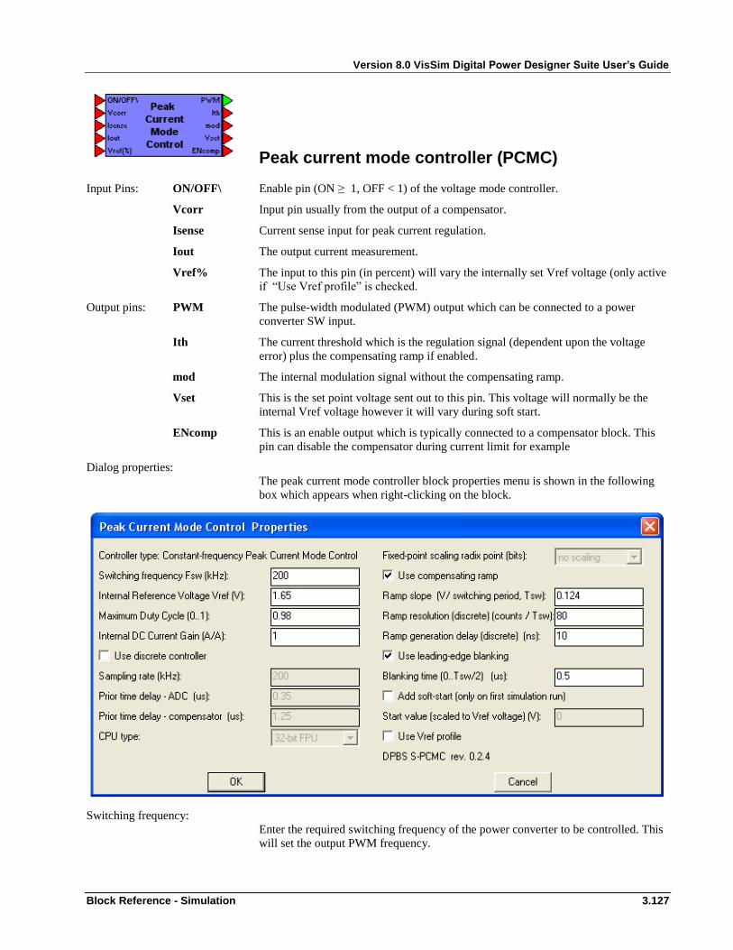
Version 8.0 VisSim Digital Power Designer Suite User’s Guide
Block Reference - Simulation 3.127
Peak current mode controller (PCMC)
Input Pins: ON/OFF\ Enable pin (ON ≥ 1, OFF < 1) of the voltage mode controller.
Vcorr Input pin usually from the output of a compensator.
Isense Current sense input for peak current regulation.
Iout The output current measurement.
Vref% The input to this pin (in percent) will vary the internally set Vref voltage (only active
if “Use Vref profile” is checked.
Output pins: PWM The pulse-width modulated (PWM) output which can be connected to a power
converter SW input.
Ith The current threshold which is the regulation signal (dependent upon the voltage
error) plus the compensating ramp if enabled.
mod The internal modulation signal without the compensating ramp.
Vset This is the set point voltage sent out to this pin. This voltage will normally be the
internal Vref voltage however it will vary during soft start.
ENcomp This is an enable output which is typically connected to a compensator block. This
pin can disable the compensator during current limit for example
Dialog properties:
The peak current mode controller block properties menu is shown in the following
box which appears when right-clicking on the block.
Switching frequency:
Enter the required switching frequency of the power converter to be controlled. This
will set the output PWM frequency.
Version 8.0 VisSim Digital Power Designer Suite User’s Guide
3.128 Block Reference - Simulation
Internal reference voltage:
Enter the reference voltage at which the scaled parameter (usually output voltage)
will be regulated.
Maximum duty cycle:
Enter the maximum duty cycle. This will limit the duty cycle so that it cannot exceed
this given value. If not used, the value should be equal to 1.
Internal DC current gain:
Enter the DC gain of the measured current used for peak current regulation.
Use discrete controller:
Check this box if a discrete controller (digital control) is to be used.
Sampling rate:
Enter the sampling rate of the controller in kilohertz. This is often the same as the
switching frequency but can be set at any other frequency.
Time delay – ADC:
Enter the time delay of the ADC. This is valid for the input voltage measurement at
Vin input pin and is also added to the internal delay of the controller.
Time delay – compensator:
Enter the prior time delay of the compensator. These two delay times should be the
same as that entered in the compensator block.
Additional internal computational delay:
Enter any additional delay for computation within the voltage mode controller. The
time delays can be adjusted to simulate any computation and sampling delay within
the digital controller. The sampling instant within the controller will occur after the
given delays so that by entering the delays, the actual sampling instant is effectively
controlled.
PWM resolution:
Enter the resolution of the output PWM (determined by the ramp) in counts /
switching period.
CPU type:
Enter the CPU type. The choices are:
1. Floating point (FPU) e.g. TI Delfino, piccolo CLA, piccolo F2806x
2. 16-bit fixed-point e.g TI TMS320F240x, MSP430
3. 32-bit fixed point e.g. TI piccolo A and piccolo B.
NOTE: If the compensator is to be simulated running in the CLA then the sampling
rate and entered time delay will reflect this and a FPU should be selected.
Fixed point scaling radix point:
Enter the fixed-point radix scaling in bits. The radix scaling is the number of bits
allocated to the whole number plus the sign bit.
e.g. For a fixed point scaling of fx4.16, 4 should selected here.
Use compensating ramp:
Check this box if slope compensation is required. For peak current control, with a
duty cycle around 50% and higher, sub-harmonic oscillations are a problem and the
control loop must be compensated, typically using a compensating ramp at the
converter switching frequency.
Ramp slope:
Enter the value of the slope of the compensating ramp in Volts / switching period.

Version 8.0 VisSim Digital Power Designer Suite User’s Guide
Block Reference - Simulation 3.129
Ramp resolution:
Enter the resolution of the compensating ramp (digital control). The ramp will be
typically quantized if it is constructed digitally (e.g. in a CLA) and the resolution can
be entered here.
Ramp generation delay:
Again if the compensating ramp is constructed digitally, a delay can be entered here
corresponding to the calculation delay of each point on the ramp.
Use leading edge blanking:
Check this box if leading-edge blanking is required. Leading-edge blanking (LEB) is
normally used in peak current mode to filter the current measurement signal, or more
precisely “ignore” it for a given window of time. This is useful to filter out any noise
impulses during the switching instant of power semiconductor devices.
Blanking time:
Enter the required blanking time in microseconds up to a maximum of half the
switching period.
Add soft start:
Check this box to enable a soft start which will be active only on the first simulation
run. The soft-start period is set automatically to 10% of the simulation end time. The
soft-start period can therefore be varied by changing the simulation end time.
Start value:
Enter the soft start initial value of the output voltage scaled with respect to Vref or
the measurement attenuation.
Use Vref profile:
Check this box to enable the use of the Vref% input pin.
Back
Average current mode controller (ACMC)
Input Pins: ON/OFF\ Enable pin (ON ≥ 1, OFF < 1) of the voltage mode controller.
Icorr Input pin usually from the output of a compensator.
Iout Converter output current measurement. This pin is for future use.
CL (=1) Current limit trigger input. A value ≥ 1 activates the current limit, switching off the
output PWM to be reset on the next switching cycle – a cycle-by-cycle (CBC)
current limit.
Vref% The input to this pin (in percent) will vary the internally set Vref voltage (only active
if “Use Vref profile” is checked.
Output pins: PWM The pulse-width modulated (PWM) output which can be connected to a power
converter SW input.
Ith Current threshold.
mod The internal modulation which along with the ramp determines the duty cycle of the
PWM output.
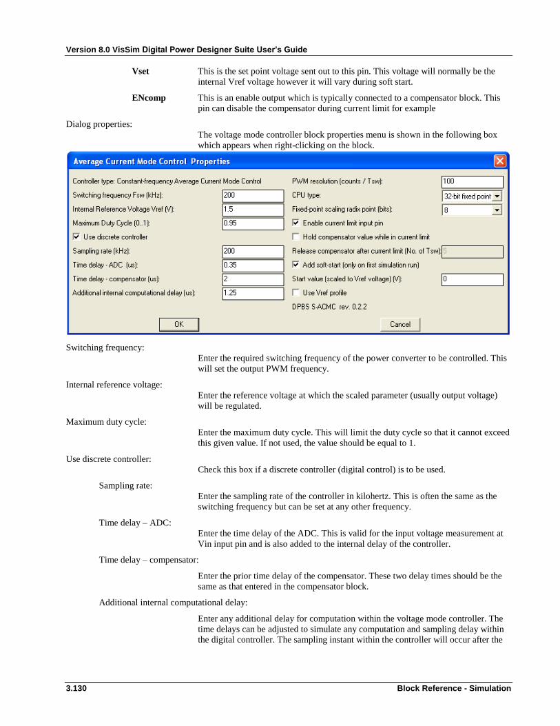
Version 8.0 VisSim Digital Power Designer Suite User’s Guide
3.130 Block Reference - Simulation
Vset This is the set point voltage sent out to this pin. This voltage will normally be the
internal Vref voltage however it will vary during soft start.
ENcomp This is an enable output which is typically connected to a compensator block. This
pin can disable the compensator during current limit for example
Dialog properties:
The voltage mode controller block properties menu is shown in the following box
which appears when right-clicking on the block.
Switching frequency:
Enter the required switching frequency of the power converter to be controlled. This
will set the output PWM frequency.
Internal reference voltage:
Enter the reference voltage at which the scaled parameter (usually output voltage)
will be regulated.
Maximum duty cycle:
Enter the maximum duty cycle. This will limit the duty cycle so that it cannot exceed
this given value. If not used, the value should be equal to 1.
Use discrete controller:
Check this box if a discrete controller (digital control) is to be used.
Sampling rate:
Enter the sampling rate of the controller in kilohertz. This is often the same as the
switching frequency but can be set at any other frequency.
Time delay – ADC:
Enter the time delay of the ADC. This is valid for the input voltage measurement at
Vin input pin and is also added to the internal delay of the controller.
Time delay – compensator:
Enter the prior time delay of the compensator. These two delay times should be the
same as that entered in the compensator block.
Additional internal computational delay:
Enter any additional delay for computation within the voltage mode controller. The
time delays can be adjusted to simulate any computation and sampling delay within
the digital controller. The sampling instant within the controller will occur after the

Version 8.0 VisSim Digital Power Designer Suite User’s Guide
Block Reference - Simulation 3.131
given delays so that by entering the delays, the actual sampling instant is effectively
controlled.
PWM resolution:
Enter the resolution of the output PWM (determined by the ramp) in counts /
switching period.
CPU type:
Enter the CPU type. The choices are:
1. Floating point (FPU) e.g. TI Delfino, piccolo CLA, piccolo F2806x
2. 16-bit fixed-point e.g TI TMS320F240x, MSP430
3. 32-bit fixed point e.g. TI piccolo A and piccolo B.
NOTE: If the compensator is to be simulated running in the CLA then the sampling
rate and entered time delay will reflect this and a FPU should be selected.
Fixed point scaling radix point:
Enter the fixed-point radix scaling in bits. The radix scaling is the number of bits
allocated to the whole number plus the sign bit.
Add soft start:
Check this box to enable a soft start which will be active only on the first simulation
run. The soft-start period is set automatically to 10% of the simulation end time. The
soft-start period can therefore be varied by changing the simulation end time.
Start value:
Enter the soft start initial value of the output voltage scaled with respect to Vref or
the measurement attenuation.
Enable current limit input pin:
Check this box to enable current limiting of the PWM output (determined by the
input pin CL).
Hold compensator value while in current limit:
If this box is checked, the compensator is disabled with its internal values “frozen”
while the current limitation persists. The compensator will be released when the
current limitation is removed.
Release compensator after current limit:
Enter the number of switching cycles that the compensator is to remain frozen after
the removal of the current limitation. The minimum amount of cycles for the control
feature to remain active is two, while in practise this would be longer due to filtering
of a noisy measurement.
Use Vref profile:
Check this box to enable the use of the input Vref% pin.
Back
Hysteretic current mode controller (HCMC)
Input Pins: ON/OFF\ Enable pin (ON ≥ 1, OFF < 1) of the voltage mode controller.

Version 8.0 VisSim Digital Power Designer Suite User’s Guide
3.132 Block Reference - Simulation
Vcorr Input pin usually from the output of a compensator.
Isense Current sense measurement input.
Iref Current reference input
Vref% The input to this pin (in percent) will vary the internally set Vref voltage (only active
if “Use Vref profile” is checked.
Output pins: PWM The pulse-width modulated (PWM) output which can be connected to a power
converter SW input.
Uth The upper band threshold.
Lth The lower band threshold.
Vset This is the set point voltage sent out to this pin. This voltage will normally be the
internal Vref voltage however it will vary during soft start.
ENcomp This is an enable output which is typically connected to a compensator block. This
pin can disable the compensator during current limit for example
Dialog properties:
The voltage mode controller block properties menu is shown in the following box
which appears when right-clicking on the block.
Internal reference voltage:
Enter the reference voltage at which the scaled parameter (usually output voltage)
will be regulated.
Maximum ON time, Ton:
Enter the maximum duty cycle. This will limit the duty cycle so that it cannot exceed
this given value. If not used, the value should be equal to 1.
Nominal average inductor current:
Enter the nominal average inductor current (equal to the output current for a buck,
the input current for a boost configuration or the output plus input current for a buck-
boost configuration).
Band limits (half window height):
Enter the band limit as a percentage of the average inductor current given above. The
bands will be ± this value with respect to the average current value.
Maximum limited input voltage at the analog input pins:
This value sets the upper limit on the input measurements of the block particularly at
the Iref input.

Version 8.0 VisSim Digital Power Designer Suite User’s Guide
Block Reference - Simulation 3.133
Minimum limited input voltage at the analog input pins:
This value sets the lower limit on the input measurements of the block.
Use Iref multiplier pin:
A multiplier signal can be used to form the current regulation waveform (usually
input current for PFC converters).
Current multiplier input Iref internal DC gain:
Enter the internal DC gain of the current reference multiplier.
Use discrete controller:
Check this box if a discrete controller (digital control) is to be used.
Sampling rate:
Enter the sampling rate of the controller in kilohertz. This is often the same as the
switching frequency but can be set at any other frequency.
Time delay – ADC:
Enter the time delay of the ADC. This is valid for the input voltage measurement at
Vin input pin and is also added to the internal delay of the controller.
Time delay – compensator:
Enter the prior time delay of the compensator. These two delay times should be the
same as that entered in the compensator block.
Additional internal computational delay:
Enter any additional delay for computation within the voltage mode controller. The
time delays can be adjusted to simulate any computation and sampling delay within
the digital controller. The sampling instant within the controller will occur after the
given delays so that by entering the delays, the actual sampling instant is effectively
controlled.
PWM resolution:
Enter the resolution of the output PWM (determined by the ramp) in counts /
switching period.
CPU type:
Enter the CPU type. The choices are:
1. Floating point (FPU) e.g. TI Delfino, piccolo CLA, piccolo F2806x
2. 16.bit fixed-point e.g TI TMS320F240x, MSP430
3. 32-bit fixed point e.g. TI piccolo A and piccolo B.
NOTE: If the compensator is to be simulated running in the CLA then the sampling
rate and entered time delay will reflect this and a FPU should be selected.
Fixed point scaling radix point:
Enter the fixed-point radix scaling in bits. The radix scaling is the number of bits
allocated to the whole number plus the sign bit.
e.g. For a fixed point scaling of fx4.16, 4 should selected here.
Add soft start:
Check this box to enable a soft start which will be active only on the first simulation
run. The soft-start period is set automatically to 10% of the simulation end time. The
soft-start period can therefore be varied by changing the simulation end time.
Start value:
Enter the soft start initial value of the output voltage scaled with respect to Vref or
the measurement attenuation.

Version 8.0 VisSim Digital Power Designer Suite User’s Guide
3.134 Block Reference - Simulation
Use Vref profile:
Check this box to enable the use of the input Vref% pin.
Zero transition current mode controller (ZCMC)
Input Pins: ON/OFF\ Enable pin (ON ≥ 1, OFF < 1) of the voltage mode controller.
Vcorr Input pin usually from the output of a compensator.
Isense Current sense measurement pin. This measurement is required for zero transition
control of the current.
Iref Current reference input. This input is multiplied with the internal correction signal in
order for the current to follow a particular form e.g in PFC applications.
Vref% The input to this pin (in percent) will vary the internally set Vref voltage (only active
if “Use Vref profile” is checked.
Output pins: PWM The pulse-width modulated (PWM) output which can be connected to a power
converter SW input.
mod The internal modulation which along with the ramp determines the duty cycle of the
PWM output.
Ramp The internal control ramp at the PWM frequency.
Vset This is the set point voltage sent out to this pin. This voltage will normally be the
internal Vref voltage however it will vary during soft start.
ENcomp This is an enable output which is typically connected to a compensator block. This
pin can disable the compensator during current limit for example
Dialog properties:
The voltage mode controller block properties menu is shown in the following box
which appears when right-clicking on the block.
Internal reference voltage:
Enter the reference voltage at which the scaled parameter (usually output voltage)
will be regulated.

Version 8.0 VisSim Digital Power Designer Suite User’s Guide
Block Reference - Simulation 3.135
Maximum ON time, Ton:
Enter the maximum ON time to limit the turn on period of the main switch.
Maximum limited input voltage at the analog input pins:
This value sets the upper limit on the input measurements of the block particularly at
the Iref input.
Minimum limited input voltage at the analog input pins:
This value sets the lower limit on the input measurements of the block.
Current limit (scaled to voltage at Isense input):
A current limit value can be set here with the appropriate scaling as seen by the input
Isense pin. The peak current in zero transition control is twice the average current
however there is no control limiting this value and therefore the additional current
limitation is required.
Use Iref multiplier pin:
A multiplier signal can be used to form the current regulation waveform (usually
input current for PFC converters).
Current multiplier input Iref internal DC gain:
Enter the internal DC gain of the current reference multiplier.
Use discrete controller:
Check this box if a discrete controller (digital control) is to be used.
Sampling rate:
Enter the sampling rate of the controller in kilohertz. This is often the same as the
switching frequency but can be set at any other frequency.
Time delay – ADC:
Enter the time delay of the ADC. This is valid for the input voltage measurement at
Vin input pin and is also added to the internal delay of the controller.
Time delay – compensator:
Enter the prior time delay of the compensator. These two delay times should be the
same as that entered in the compensator block.
Additional internal computational delay:
Enter any additional delay for computation within the voltage mode controller. The
time delays can be adjusted to simulate any computation and sampling delay within
the digital controller. The sampling instant within the controller will occur after the
given delays so that by entering the delays, the actual sampling instant is effectively
controlled.
PWM resolution:
Enter the resolution of the output PWM (determined by the ramp) in counts /
switching period.
CPU type:
Enter the CPU type. The choices are:
1. Floating point (FPU) e.g. TI Delfino, piccolo CLA, piccolo F2806x
2. 16-bit fixed-point e.g TI TMS320F240x, MSP430
3. 32-bit fixed point e.g. TI piccolo A and piccolo B.
NOTE: If the compensator is to be simulated running in the CLA then the sampling
rate and entered time delay will reflect this and a FPU should be selected.
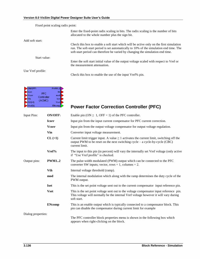
Version 8.0 VisSim Digital Power Designer Suite User’s Guide
3.136 Block Reference - Simulation
Fixed point scaling radix point:
Enter the fixed-point radix scaling in bits. The radix scaling is the number of bits
allocated to the whole number plus the sign bit.
Add soft start:
Check this box to enable a soft start which will be active only on the first simulation
run. The soft-start period is set automatically to 10% of the simulation end time. The
soft-start period can therefore be varied by changing the simulation end time.
Start value:
Enter the soft start initial value of the output voltage scaled with respect to Vref or
the measurement attenuation.
Use Vref profile:
Check this box to enable the use of the input Vref% pin.
Power Factor Correction Controller (PFC)
Input Pins: ON/OFF\ Enable pin (ON ≥ 1, OFF < 1) of the PFC controller.
Icorr Input pin from the input current compensator for PFC current correction.
Vcorr Input pin from the output voltage compensator for output voltage regulation.
Vin Converter input voltage measurement.
CL (=1) Current limit trigger input. A value ≥ 1 activates the current limit, switching off the
output PWM to be reset on the next switching cycle – a cycle-by-cycle (CBC)
current limit.
Vref% The input to this pin (in percent) will vary the internally set Vref voltage (only active
if “Use Vref profile” is checked.
Output pins: PWM1..2 The pulse-width modulated (PWM) output which can be connected to the PFC
converter SW inputs; vector, rows = 1, columns = 2.
Vth Internal voltage threshold (ramp).
mod The internal modulation which along with the ramp determines the duty cycle of the
PWM output.
Iset This is the set point voltage sent out to the current compensator input reference pin.
Vset This is the set point voltage sent out to the voltage compensator input reference pin.
This voltage will normally be the internal Vref voltage however it will vary during
soft start.
ENcomp This is an enable output which is typically connected to a compensator block. This
pin can disable the compensator during current limit for example
Dialog properties:
The PFC controller block properties menu is shown in the following box which
appears when right-clicking on the block.

Version 8.0 VisSim Digital Power Designer Suite User’s Guide
Block Reference - Simulation 3.137
PFC Controller type:
The choices here are:
1. Single stage PFC controller (PWM1 controlled, PWM2 = 0)
2. Dual-interleaved PFC controller (PWM2 slaved to PWM1 at 180°).
3. PWM bridge PFC controller (PWM1 an PWM2 on alternately).
4. Bridgeless PFC controller (PWM1 and PWM2 individually controlled).
Maintain PWM high during opposite half-cycle:
For the bridgeless PFC controller only, the second PWM switch for the return
current can be maintained on during the opposing half cycle of the mains input.
Switching frequency:
Enter the required switching frequency of the power converter to be controlled. This
will set the output PWM frequency.
Internal reference voltage:
Enter the reference voltage at which the scaled parameter (usually output voltage)
will be regulated.
Maximum duty cycle:
Enter the maximum duty cycle. This will limit the duty cycle so that it cannot exceed
this given value. If not used, the value should be equal to 1.
Input voltage measurement offset:
The input AC voltage maybe offset to allow it to measured by a sensor that does not
accept negative voltages. In that case, enter the voltage of the input voltage
measurement offset here.
Hysteresis on input voltage measurement zero detection:
For noisy input AC voltages it may be advantageous to include a hysteresis on the
detection of the zero crossings of the input AC mains voltages. This is maly used for
the bridgeless PFC controller where the positive and negative halves must be
detected. The hysteresis will be ±half of the given value.
Use discrete controller:
Check this box if a discrete controller (digital control) is to be used.
Version 8.0 VisSim Digital Power Designer Suite User’s Guide
3.138 Block Reference - Simulation
Sampling rate:
Enter the sampling rate of the controller in kilohertz. This is often the same as the
switching frequency but can be set at any other frequency.
Time delay – ADC:
Enter the time delay of the ADC. This is valid for the input voltage measurement at
Vin input pin and is also added to the internal delay of the controller.
Time delay – compensator:
Enter the prior time delay of the compensator. These two delay times should be the
same as that entered in the compensator block.
Additional internal computational delay:
Enter any additional delay for computation within the voltage mode controller. The
time delays can be adjusted to simulate any computation and sampling delay within
the digital controller. The sampling instant within the controller will occur after the
given delays so that by entering the delays, the actual sampling instant is effectively
controlled.
PWM resolution:
Enter the resolution of the output PWM (determined by the ramp) in counts /
switching period.
CPU type:
Enter the CPU type. The choices are:
1. Floating point (FPU) e.g. TI Delfino, piccolo CLA, piccolo F2806x
2. 16-bit fixed-point e.g TI TMS320F240x, MSP430
3. 32-bit fixed point e.g. TI piccolo A and piccolo B.
NOTE: If the compensator is to be simulated running in the CLA then the sampling
rate and entered time delay will reflect this and a FPU should be selected.
Fixed point scaling radix point:
Enter the fixed-point radix scaling in bits. The radix scaling is the number of bits
allocated to the whole number plus the sign bit.
Enable input voltage feed forward compensation:
Check this box to enable input voltage feed-forward compensation.
Nominal input (reference) voltage Vrms:
Enter the nominal rms input voltage in volts.
Input voltage measurement attenuation:
Enter the attenuation on the input voltage measurement seen at the Vin input pin of
the controller.
Enable current limit input pin:
Check this box to enable current limiting of the PWM output (determined by the
input pin CL).
Hold compensator value while in current limit:
If this box is checked, the compensator is disabled with its internal values “frozen”
while the current limitation persists. The compensator will be released when the
current limitation is removed.
Release compensator after current limit:
Enter the number of switching cycles that the compensator is to remain frozen after
the removal of the current limitation. The minimum amount of cycles for the control

Version 8.0 VisSim Digital Power Designer Suite User’s Guide
Block Reference - Simulation 3.139
feature to remain active is two, while in practise this would be longer due to filtering
of a noisy measurement.
Add soft start:
Check this box to enable a soft start which will be active only on the first simulation
run. The soft-start period is set automatically to 10% of the simulation end time. The
soft-start period can therefore be varied by changing the simulation end time.
Start value:
Enter the soft start initial value of the output voltage scaled with respect to Vref or
the measurement attenuation.
Use Vref profile:
Check this box to enable the use of the input Vref% pin.
Thyristor Rectifier Controller
The thyristor rectifier controller is suitable for driving controlled rectifiers using
thyristor switches. It can drive single-phase and three-phase controlled-rectifiers,
both half-wave and full-wave.
Input Pins: Vac Input AC voltage pin (V); vector, rows = 1, columns = 3. For single-phase, only the
first phase is considered.
DC The control input expressed as a duty cycle from 0 to 1. Note that the DC input will
not be linearly proportional to the output voltage but rather inversely proportional to
the firing angle. An input of DC = 0 corresponds to an alpha of 90°, while a DC = 1
input corresponds to an alpha of 0°.
CL (=1) Current limit trigger input. A value ≥ 1 activates the current limit, switching off the
output PWM to be reset on the next switching cycle – a cycle-by-cycle (CBC)
current limit.
Vref% The input to this pin (in percent) will vary the internally set Vref voltage (only active
if “Use Vref profile” is checked.
Output pins: TH[1..6] The thyristor control output pulses which can be connected to a thyrsitor rectifier TH
inputs; vector, rows = 1, columns = 6. Only the first four are active for a single-phase
controller.
Vset This is the set point voltage sent out to the voltage compensator input reference pin.
This voltage will normally be the internal Vref voltage however it will vary during
soft start.
F (Hz) The internally measured mains frequency in Hertz.
alpha The current firing angle in degrees.
Dialog properties:
The thyristor rectifier controller block properties menu is shown in the following box
which appears when right-clicking on the block.
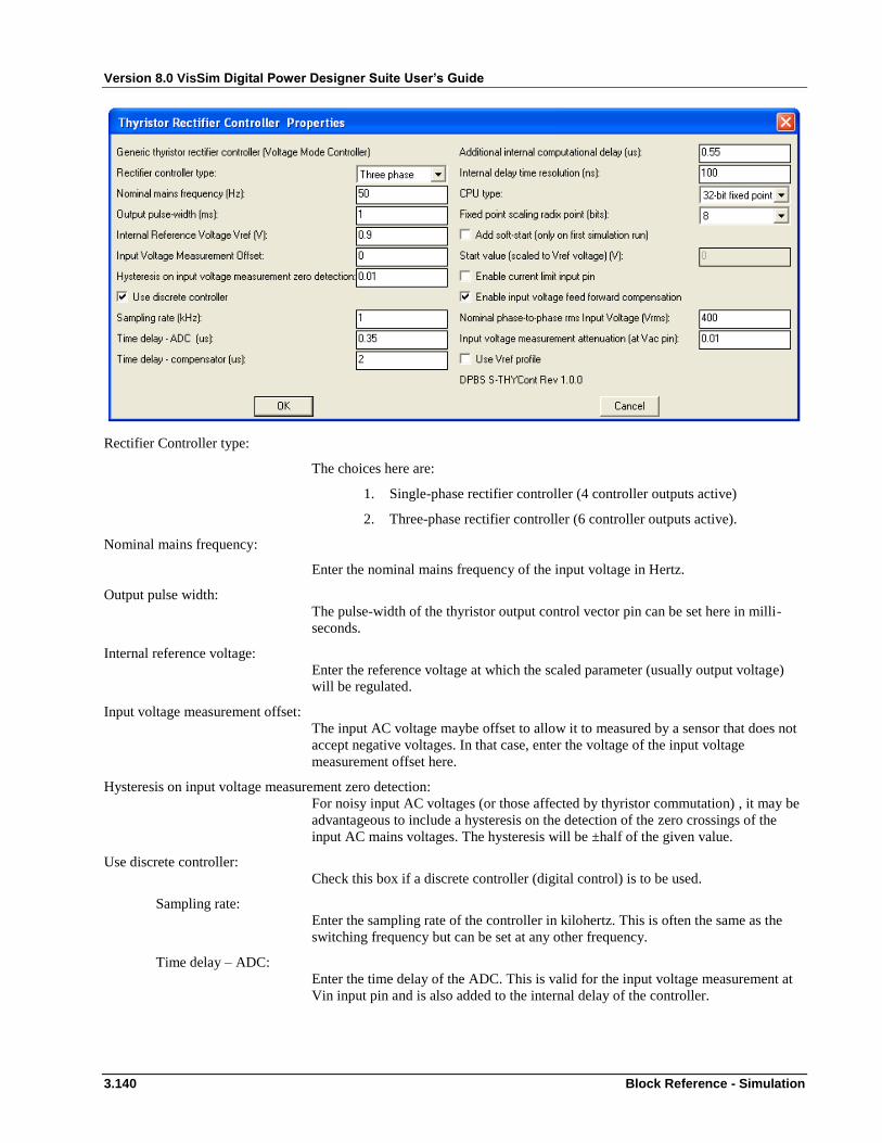
Version 8.0 VisSim Digital Power Designer Suite User’s Guide
3.140 Block Reference - Simulation
Rectifier Controller type:
The choices here are:
1. Single-phase rectifier controller (4 controller outputs active)
2. Three-phase rectifier controller (6 controller outputs active).
Nominal mains frequency:
Enter the nominal mains frequency of the input voltage in Hertz.
Output pulse width:
The pulse-width of the thyristor output control vector pin can be set here in milli-
seconds.
Internal reference voltage:
Enter the reference voltage at which the scaled parameter (usually output voltage)
will be regulated.
Input voltage measurement offset:
The input AC voltage maybe offset to allow it to measured by a sensor that does not
accept negative voltages. In that case, enter the voltage of the input voltage
measurement offset here.
Hysteresis on input voltage measurement zero detection:
For noisy input AC voltages (or those affected by thyristor commutation) , it may be
advantageous to include a hysteresis on the detection of the zero crossings of the
input AC mains voltages. The hysteresis will be ±half of the given value.
Use discrete controller:
Check this box if a discrete controller (digital control) is to be used.
Sampling rate:
Enter the sampling rate of the controller in kilohertz. This is often the same as the
switching frequency but can be set at any other frequency.
Time delay – ADC:
Enter the time delay of the ADC. This is valid for the input voltage measurement at
Vin input pin and is also added to the internal delay of the controller.

Version 8.0 VisSim Digital Power Designer Suite User’s Guide
Block Reference - Simulation 3.141
Time delay – compensator:
Enter the prior time delay of the compensator. These two delay times should be the
same as that entered in the compensator block.
Additional internal computational delay:
Enter any additional delay for computation within the voltage mode controller. The
time delays can be adjusted to simulate any computation and sampling delay within
the digital controller. The sampling instant within the controller will occur after the
given delays so that by entering the delays, the actual sampling instant is effectively
controlled.
PWM resolution:
Enter the resolution of the output PWM (determined by the ramp) in counts /
switching period.
CPU type:
Enter the CPU type. The choices are:
4. Floating point (FPU) e.g. TI Delfino, piccolo CLA, piccolo F2806x
5. 16-bit fixed-point e.g TI TMS320F240x, MSP430
6. 32-bit fixed point e.g. TI piccolo A and piccolo B.
NOTE: If the compensator is to be simulated running in the CLA then the sampling
rate and entered time delay will reflect this and a FPU should be selected.
Fixed point scaling radix point:
Enter the fixed-point radix scaling in bits. The radix scaling is the number of bits
allocated to the whole number plus the sign bit.
Add soft start:
Check this box to enable a soft start which will be active only on the first simulation
run. The soft-start period is set automatically to 10% of the simulation end time. The
soft-start period can therefore be varied by changing the simulation end time.
Start value:
Enter the soft start initial value of the output voltage scaled with respect to Vref or
the measurement attenuation.
Enable current limit input pin:
Check this box to enable current limiting (enables the input pin CL).
Enable input voltage feed forward compensation:
Check this box to enable input voltage feed-forward compensation.
Nominal phase-to-phase rms input voltage Vrms:
Enter the nominal phase-to-phase rms input voltage in volts for a three-phase
controller or the nominal phase-to-neutral rms input voltage for a single-phase
controller.
Input voltage measurement attenuation (at Vac input pin):
Enter the attenuation on the input voltage measurement seen at the Vac input pin of
the controller.
Use Vref profile:
Check this box to enable the use of the input Vref% pin.
Back

Version 8.0 VisSim Digital Power Designer Suite User’s Guide
3.142 Block Reference - Simulation
Compensators
The aim of a compensator as used in power converter control loops (digital or
analog) is to provide as much DC gain as possible in order to eliminate any steady
state error in the control loop regulation, to provide the required poles and zeros to
compensate for those present together within the power converter and control
technique, ensure sufficient closed-loop attenuation at the switching frequency and
attenuate any line or input frequency. There are 7 different compensators available in
the simulation section of the digital power block set, all with a pole at the origin to
provide a high DC gain and each with a different number of poles and zeros.
The type 1, 2, 3 and 3p3z compensators can be applied by directly entering the
required poles and zeros, while the PI and PID compensators can be applied using
the familiar Proportional-Integral-Differential gains.
Conversion between the PID gains and the compensator poles and zeros can be
performed using the compensator tools in the tools section of the digital power block
set.
Type 1 compensator
The type 1 compensator is basically an I-compensator which only has an integral
part. It is a first order compensator which only has one pole at the origin and no zero.
It is rarely used in digital control because adding additional poles or zeros do not
complicate things too much and the additional poles and zeros allow better
performance. The type 1 compensator can be used successfully in cruder analog
current mode control if the ESR zero is chosen appropriately (the output capacitor
type).
This compensator has the transfer function:
Or expressed as a discrete compensator (when selected):
where p0 is the pole at the origin and Ts is the compensator sampling time.
Input pins: EN Enables the compensator for execution. A value < 1 at this pin will hold the current
values within the compensator until the EN pin returns to ≥ 1.
Vsense(-) The voltage sensing input (negative input to the compensator) in Volts.
Vset(+) The set point voltage (positive input) in Volts.
Reset A value ≥ 1 at this pin will hold the compensator in reset, resetting the internal
integrators to zero.
Output pins: Vcorr The output of the compensator.
H1 s( )p0
s
H1 z( ) p0 Tsz
z 1

Version 8.0 VisSim Digital Power Designer Suite User’s Guide
Block Reference - Simulation 3.143
Dialog properties:
The type 1 compensator block properties menu is shown in the following box which
appears when right-clicking on the block.
Vsense input internal DC gain:
Enter the DC gain adjustment (if none = 1) before the error voltage is calculated and
the voltage sensed is fed to the internal compensator input.
Internally:
Verr = Vset – Vsense*DCgain.
Zero pole Fp0:
Enter the value of the compensator pole at the origin in kilohertz.
Compensator high limit:
Enter the high level limit of the compensator.
Compensator low limit:
Enter the low-level limit of the compensator. NOTE that these limits are anti-windup
limits.
Use discrete compensator:
Check this box if a discrete compensator is to be used in a simulation (digital
control).
Sampling rate:
Enter the discrete compensator sampling rate.
NOTE: If an external file is used for the discrete coefficients, the sampling rate used
to generate those coefficients must be equal to the value entered here. If the poles
and zeros are entered manually, the discrete compensator coefficients will be
generated for the entered sample rate.
Total prior time delay – ADC sampling:
Enter any prior time delay (usually the sampling time of an ADC). The input values
will be sampled after this time delay.
Additional internal computational delay:
Enter the additional time delay which would correspond to the time it takes for the
compensator to calculate its output value. The output value of the compensator will
be updated after this time delay plus the prior time delay.

Version 8.0 VisSim Digital Power Designer Suite User’s Guide
3.144 Block Reference - Simulation
CPU type:
Enter the CPU type. The choices are:
1. Floating point (FPU) e.g. TI Delfino, piccolo CLA, piccolo F2806x
2. 16-bit fixed-point e.g TI TMS320F240x, MSP430
3. 32-bit fixed point e.g. TI piccolo A and piccolo B.
NOTE: If the compensator is to be simulated running in the CLA then the sampling
rate and entered time delay will reflect this and a FPU should be selected.
Fixed point scaling radix point:
Enter the fixed-point radix scaling in bits. The radix scaling is the number of bits
allocated to the whole number plus the sign bit.
e.g. For a fixed point scaling of fx4.16, 4 should selected here.
Back
Type 2 compensator
The type 2 compensator is a second order compensator with two poles (one at the
origin) and a zero. This compensator is typically used in peak current mode control.
This compensator has the transfer function:
Or expressed as a discrete compensator (when selected):
where the coefficients Kz, Bn and An are calculated internally in the compensator
block using the bi-linear (Tustin) transform or can be imported from an external file.
Input pins: EN Enables the compensator for execution. A value < 1 at this pin will hold the current
values within the compensator until the EN pin returns to ≥ 1.
Vsense(-) The voltage sensing input (negative input to the compensator) in Volts.
Vset(+) The set point voltage (positive input) in Volts.
Reset A value ≥ 1 at this pin will hold the compensator in reset, resetting the internal
integrators to zero.
Output pins: Vcorr The output of the compensator.
H2 s( )p0
s
s
z1
1
s
p1
1
H2 z( ) Kz
z2
B1 z B0
z2
A1 z A0
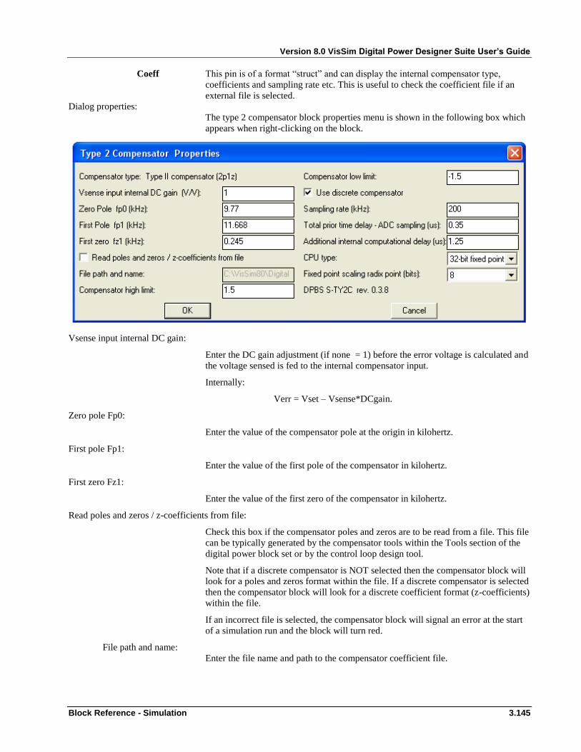
Version 8.0 VisSim Digital Power Designer Suite User’s Guide
Block Reference - Simulation 3.145
Coeff This pin is of a format “struct” and can display the internal compensator type,
coefficients and sampling rate etc. This is useful to check the coefficient file if an
external file is selected.
Dialog properties:
The type 2 compensator block properties menu is shown in the following box which
appears when right-clicking on the block.
Vsense input internal DC gain:
Enter the DC gain adjustment (if none = 1) before the error voltage is calculated and
the voltage sensed is fed to the internal compensator input.
Internally:
Verr = Vset – Vsense*DCgain.
Zero pole Fp0:
Enter the value of the compensator pole at the origin in kilohertz.
First pole Fp1:
Enter the value of the first pole of the compensator in kilohertz.
First zero Fz1:
Enter the value of the first zero of the compensator in kilohertz.
Read poles and zeros / z-coefficients from file:
Check this box if the compensator poles and zeros are to be read from a file. This file
can be typically generated by the compensator tools within the Tools section of the
digital power block set or by the control loop design tool.
Note that if a discrete compensator is NOT selected then the compensator block will
look for a poles and zeros format within the file. If a discrete compensator is selected
then the compensator block will look for a discrete coefficient format (z-coefficients)
within the file.
If an incorrect file is selected, the compensator block will signal an error at the start
of a simulation run and the block will turn red.
File path and name:
Enter the file name and path to the compensator coefficient file.
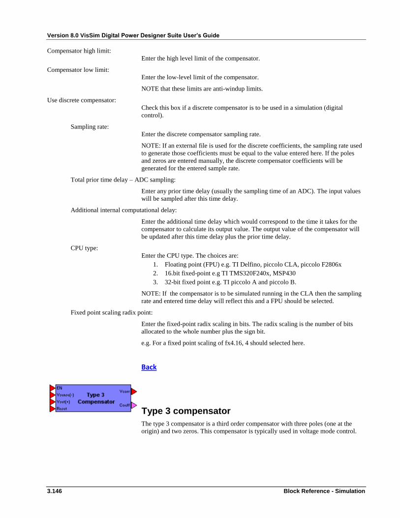
Version 8.0 VisSim Digital Power Designer Suite User’s Guide
3.146 Block Reference - Simulation
Compensator high limit:
Enter the high level limit of the compensator.
Compensator low limit:
Enter the low-level limit of the compensator.
NOTE that these limits are anti-windup limits.
Use discrete compensator:
Check this box if a discrete compensator is to be used in a simulation (digital
control).
Sampling rate:
Enter the discrete compensator sampling rate.
NOTE: If an external file is used for the discrete coefficients, the sampling rate used
to generate those coefficients must be equal to the value entered here. If the poles
and zeros are entered manually, the discrete compensator coefficients will be
generated for the entered sample rate.
Total prior time delay – ADC sampling:
Enter any prior time delay (usually the sampling time of an ADC). The input values
will be sampled after this time delay.
Additional internal computational delay:
Enter the additional time delay which would correspond to the time it takes for the
compensator to calculate its output value. The output value of the compensator will
be updated after this time delay plus the prior time delay.
CPU type:
Enter the CPU type. The choices are:
1. Floating point (FPU) e.g. TI Delfino, piccolo CLA, piccolo F2806x
2. 16.bit fixed-point e.g TI TMS320F240x, MSP430
3. 32-bit fixed point e.g. TI piccolo A and piccolo B.
NOTE: If the compensator is to be simulated running in the CLA then the sampling
rate and entered time delay will reflect this and a FPU should be selected.
Fixed point scaling radix point:
Enter the fixed-point radix scaling in bits. The radix scaling is the number of bits
allocated to the whole number plus the sign bit.
e.g. For a fixed point scaling of fx4.16, 4 should selected here.
Back
Type 3 compensator
The type 3 compensator is a third order compensator with three poles (one at the
origin) and two zeros. This compensator is typically used in voltage mode control.
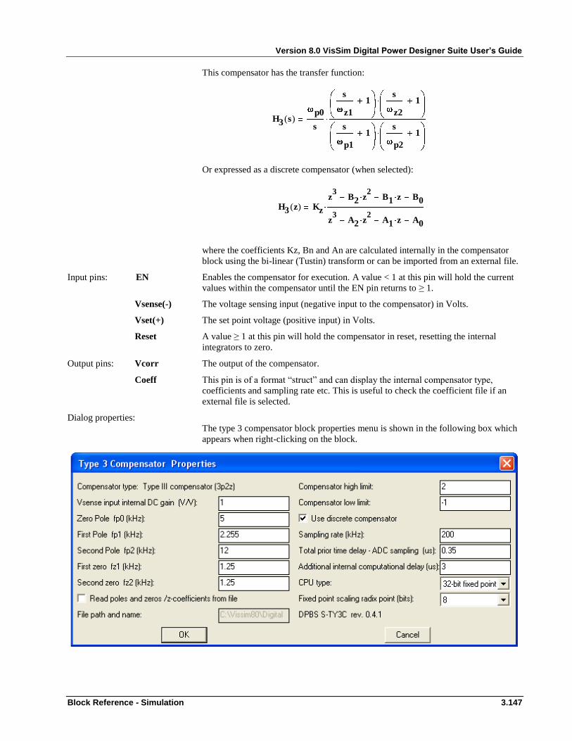
Version 8.0 VisSim Digital Power Designer Suite User’s Guide
Block Reference - Simulation 3.147
This compensator has the transfer function:
Or expressed as a discrete compensator (when selected):
where the coefficients Kz, Bn and An are calculated internally in the compensator
block using the bi-linear (Tustin) transform or can be imported from an external file.
Input pins: EN Enables the compensator for execution. A value < 1 at this pin will hold the current
values within the compensator until the EN pin returns to ≥ 1.
Vsense(-) The voltage sensing input (negative input to the compensator) in Volts.
Vset(+) The set point voltage (positive input) in Volts.
Reset A value ≥ 1 at this pin will hold the compensator in reset, resetting the internal
integrators to zero.
Output pins: Vcorr The output of the compensator.
Coeff This pin is of a format “struct” and can display the internal compensator type,
coefficients and sampling rate etc. This is useful to check the coefficient file if an
external file is selected.
Dialog properties:
The type 3 compensator block properties menu is shown in the following box which
appears when right-clicking on the block.
H3 s( )p0
s
s
z1
1s
z2
1
s
p1
1s
p2
1
H3 z( ) Kz
z3
B2 z2
B1 z B0
z3
A2 z2
A1 z A0
Version 8.0 VisSim Digital Power Designer Suite User’s Guide
3.148 Block Reference - Simulation
Vsense input internal DC gain:
Enter the DC gain adjustment (if none = 1) before the error voltage is calculated and
the voltage sensed is fed to the internal compensator input.
Internally:
Verr = Vset – Vsense*DCgain.
Zero pole Fp0:
Enter the value of the compensator pole at the origin in kilohertz.
First pole Fp1:
Enter the value of the first pole of the compensator in kilohertz.
Second pole Fp2:
Enter the value of the second pole of the compensator in kilohertz
First zero Fz1:
Enter the value of the first zero of the compensator in kilohertz.
Second zero Fz2:
Enter the value of the second zero of the compensator in kilohertz.
Read poles and zeros / z-coefficients from file:
Check this box if the compensator poles and zeros are to be read from a file. This file
can be typically generated by the compensator tools within the Tools section of the
digital power block set or by the control loop design tool.
Note that if a discrete compensator is NOT selected then the compensator block will
look for a poles and zeros format within the file. If a discrete compensator is selected
then the compensator block will look for a discrete coefficient format (z-coefficients)
within the file.
If an incorrect file is selected, the compensator block will signal an error at the start
of a simulation run and the block will turn red.
File path and name:
Enter the file name and path to the compensator coefficient file.
Compensator High limit:
Enter the high level limit of the compensator.
Compensator low limit:
Enter the low-level limit of the compensator.
NOTE that these limits are anti-windup limits.
Use discrete compensator:
Check this box if a discrete compensator is to be used in a simulation (digital
control).
Sampling rate:
Enter the discrete compensator sampling rate.
NOTE: If an external file is used for the discrete coefficients, the sampling rate used
to generate those coefficients must be equal to the value entered here. If the poles
and zeros are entered manually, the discrete compensator coefficients will be
generated for the entered sample rate.
Total prior time delay – ADC sampling:
Enter any prior time delay (usually the sampling time of an ADC). The input values
will be sampled after this delay.
Version 8.0 VisSim Digital Power Designer Suite User’s Guide
Block Reference - Simulation 3.149
Additional internal computational delay:
Enter the additional time delay which would correspond to the time it takes for the
compensator to calculate its output value. The output value of the compensator will
be updated after this time delay plus the prior time delay.
CPU type:
Enter the CPU type. The choices are:
1. Floating point (FPU) e.g. TI Delfino, piccolo CLA, piccolo F2806x
2. 16.bit fixed-point e.g TI TMS320F240x, MSP430
3. 32-bit fixed point e.g. TI piccolo A and piccolo B.
NOTE: If the compensator is to be simulated running in the CLA then the sampling
rate and entered time delay will reflect this and a FPU should be selected.
Fixed point scaling radix point:
Enter the fixed-point radix scaling in bits. The radix scaling is the number of bits
allocated to the whole number plus the sign bit.
e.g. For a fixed point scaling of fx4.16, 4 should selected here.
Back
PI compensator
The PI compensator is a proportional + integral gain compensator . It is a first order
compensator with one pole at the origin and one zero. This block enables the setting
of the coefficients using the familiar proportional and integral gains rather than the
poles and zeros. This type of compensator is popular in certain applications (current
mode control or auxiliary loops such as paralleling) due to its simplicity (only two
parameters need to be set).
This compensator has the transfer function:
Or expressed as a discrete compensator (when selected):
where the coefficients Kp and Ki are the proportional and integral gain coefficients
and Ts is the compensator sampling time.
Input pins: EN Enables the compensator for execution. A value < 1 at this pin will hold the current
values within the compensator until the EN pin returns to ≥ 1.
Vsense(-) The voltage sensing input (negative input to the compensator) in Volts.
Vset(+) The set point voltage (positive input) in Volts.
Hpi s( ) KpKi
s
Hpi z( ) Kp Ki Tsz
z 1
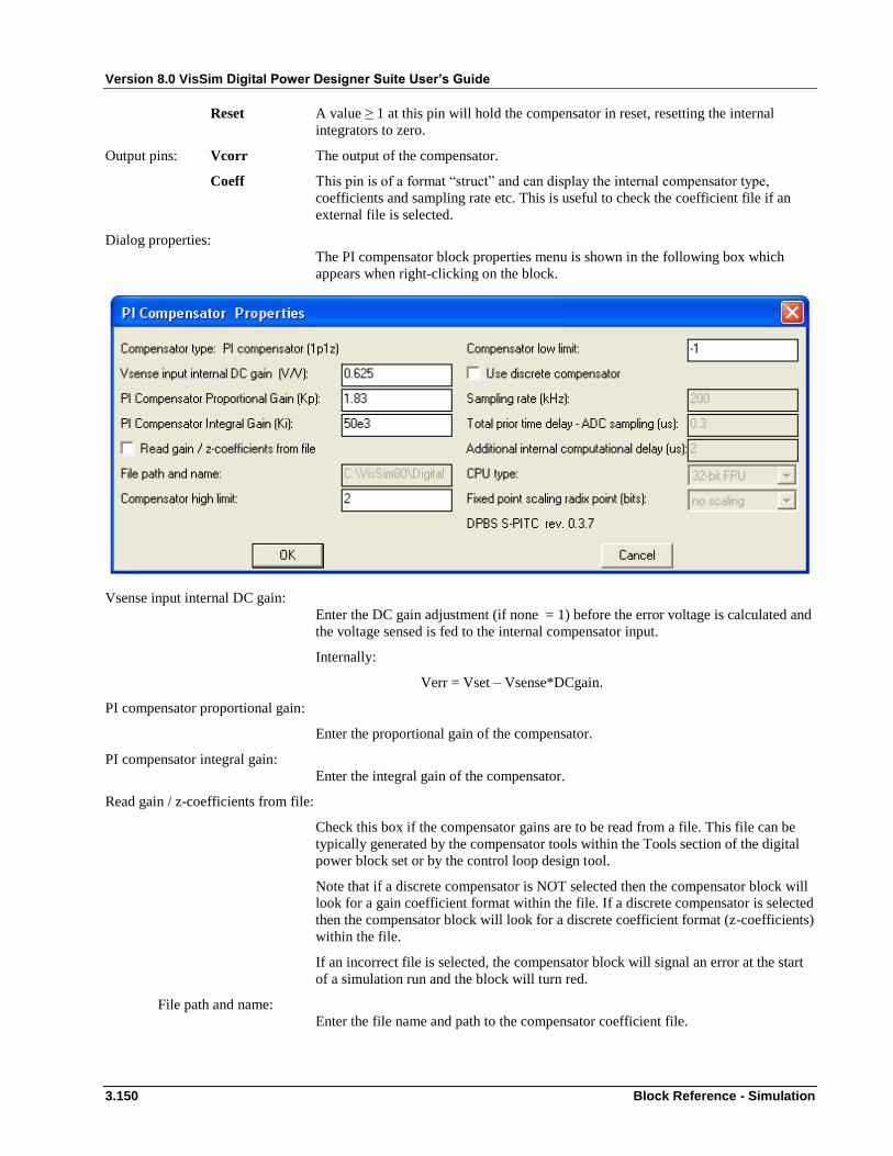
Version 8.0 VisSim Digital Power Designer Suite User’s Guide
3.150 Block Reference - Simulation
Reset A value ≥ 1 at this pin will hold the compensator in reset, resetting the internal
integrators to zero.
Output pins: Vcorr The output of the compensator.
Coeff This pin is of a format “struct” and can display the internal compensator type,
coefficients and sampling rate etc. This is useful to check the coefficient file if an
external file is selected.
Dialog properties:
The PI compensator block properties menu is shown in the following box which
appears when right-clicking on the block.
Vsense input internal DC gain:
Enter the DC gain adjustment (if none = 1) before the error voltage is calculated and
the voltage sensed is fed to the internal compensator input.
Internally:
Verr = Vset – Vsense*DCgain.
PI compensator proportional gain:
Enter the proportional gain of the compensator.
PI compensator integral gain:
Enter the integral gain of the compensator.
Read gain / z-coefficients from file:
Check this box if the compensator gains are to be read from a file. This file can be
typically generated by the compensator tools within the Tools section of the digital
power block set or by the control loop design tool.
Note that if a discrete compensator is NOT selected then the compensator block will
look for a gain coefficient format within the file. If a discrete compensator is selected
then the compensator block will look for a discrete coefficient format (z-coefficients)
within the file.
If an incorrect file is selected, the compensator block will signal an error at the start
of a simulation run and the block will turn red.
File path and name:
Enter the file name and path to the compensator coefficient file.

Version 8.0 VisSim Digital Power Designer Suite User’s Guide
Block Reference - Simulation 3.151
Compensator High limit:
Enter the high level limit of the compensator.
Compensator low limit:
Enter the low-level limit of the compensator.
NOTE that these limits are anti-windup limits.
Use discrete compensator:
Check this box if a discrete compensator is to be used in a simulation (digital
control).
Sampling rate:
Enter the discrete compensator sampling rate.
NOTE: If an external file is used for the discrete coefficients, the sampling rate used
to generate those coefficients must be equal to the value entered here. If the poles
and zeros are entered manually, the discrete compensator coefficients will be
generated for the entered sample rate.
Total prior time delay – ADC sampling:
Enter any prior time delay (usually the sampling time of an ADC).
Additional internal computational delay:
Enter the additional time delay which would correspond to the time it takes for the
compensator to calculate its output value.
CPU type:
Enter the CPU type. The choices are:
1. Floating point (FPU) e.g. TI Delfino, piccolo CLA, piccolo F2806x
2. 16.bit fixed-point e.g TI TMS320F240x, MSP430
3. 32-bit fixed point e.g. TI piccolo A and piccolo B.
NOTE: If the compensator is to be simulated running in the CLA then the sampling
rate and entered time delay will reflect this and a FPU should be selected.
Fixed point scaling radix point:
Enter the fixed-point radix scaling in bits. The radix scaling is the number of bits
allocated to the whole number plus the sign bit.
e.g. For a fixed point scaling of fx4.16, 4 should selected here.
Back
PID compensator (traditional)
This compensator is a second order compensator allowing the setting of the
proportional, integral and differential gains. The differential part of the transfer
function is approximated to the difference of the input over the last two samples,
multiplied by the differential gain. This compensator has two zeros and one pole at
the origin and as such cannot be realized in a practical transfer function. This type of
compensator is rarely used in digital power due to the sensitivity of the differential
part to noise and it is normally replaced by the 2p2z PID compensator.

Version 8.0 VisSim Digital Power Designer Suite User’s Guide
3.152 Block Reference - Simulation
This compensator has the transfer function:
Or expressed as a discrete compensator (when selected):
where the coefficients Kp, Ki and Kd are the proportional, integral and differential
gain coefficients and Ts is the compensator sampling time.
Input pins: EN Enables the compensator for execution. A value < 1 at this pin will hold the current
values within the compensator until the EN pin returns to ≥ 1.
Vsense(-) The voltage sensing input (negative input to the compensator) in Volts.
Vset(+) The set point voltage (positive input) in Volts.
Reset A value ≥ 1 at this pin will hold the compensator in reset, resetting the internal
integrators to zero.
Output pins: Vcorr The output of the compensator.
Coeff This pin is of a format “struct” and can display the internal compensator type,
coefficients and sampling rate etc. This is useful to check the coefficient file if an
external file is selected.
Dialog properties:
The PID compensator properties menu is shown in the following box which appears
when right-clicking on the block.
Vsense input internal DC gain:
Enter the DC gain adjustment (if none = 1) before the error voltage is calculated and
the voltage sensed is fed to the internal compensator input.
Internally:
Verr = Vset – Vsense*DCgain.
Hpid s( ) KpKi
sKd s
Hpid z( ) Kp Ki Tsz
z 1
Kd
Ts
z 1
z

Version 8.0 VisSim Digital Power Designer Suite User’s Guide
Block Reference - Simulation 3.153
PID compensator proportional gain:
Enter the proportional gain of the compensator.
PID compensator integral gain:
Enter the integral gain of the compensator.
PID compensator differential gain:
Enter the differential gain of the compensator.
Read gain / z-coefficients from file:
Check this box if the compensator poles and zeros are to be read from a file. This file
can be typically generated by the compensator tools within the Tools section of the
digital power block set or by the control loop design tool.
Note that if a discrete compensator is NOT selected then the compensator block will
look for a poles and zeros format within the file. If a discrete compensator is selected
then the compensator block will look for a discrete coefficient format (z-coefficients)
within the file.
If an incorrect file is selected, the compensator block will signal an error at the start
of a simulation run and the block will turn red.
File path and name:
Enter the file name and path to the compensator coefficient file.
Compensator High limit:
Enter the high level limit of the compensator.
Compensator low limit:
Enter the low-level limit of the compensator.
NOTE that these limits are anti-windup limits.
Use discrete compensator:
Check this box if a discrete compensator is to be used in a simulation (digital
control).
Sampling rate:
Enter the discrete compensator sampling rate.
NOTE: If an external file is used for the discrete coefficients, the sampling rate used
to generate those coefficients must be equal to the value entered here. If the poles
and zeros are entered manually, the discrete compensator coefficients will be
generated for the entered sample rate.
Total prior time delay – ADC sampling:
Enter any prior time delay (usually the sampling time of an ADC).
Additional internal computational delay:
Enter the additional time delay which would correspond to the time it takes for the
compensator to calculate its output value.
CPU type:
Enter the CPU type. The choices are:
1. Floating point (FPU) e.g. TI Delfino, piccolo CLA, piccolo F2806x
2. 16.bit fixed-point e.g TI TMS320F240x, MSP430
3. 32-bit fixed point e.g. TI piccolo A and piccolo B.
NOTE: If the compensator is to be simulated running in the CLA then the sampling
rate and entered time delay will reflect this and a FPU should be selected.

Version 8.0 VisSim Digital Power Designer Suite User’s Guide
3.154 Block Reference - Simulation
Fixed point scaling radix point:
Enter the fixed-point radix scaling in bits. The radix scaling is the number of bits
allocated to the whole number plus the sign bit.
E.g. For a fixed point scaling of fx4.16, 4 should selected here.
Back
PID compensator (2p2z)
This compensator is a PID compensator where the proportional, integral and
differential gain terms can be set along with a fourth parameter which applies a low-
pass filter on the differential term. The differential term low-pass filter coefficient is
set relative to the differential gain using the value N. The compensator is a second
order compensator with two poles (one at the origin) and two zeros. This type of
compensator is popular in digital control.
This compensator has the transfer function:
Or expressed as a discrete compensator (when selected):
where the coefficients Kz, Bn and An are calculated internally in the compensator
block using the bi-linear (Tustin) transform or can be imported from an external file.
Input pins: EN Enables the compensator for execution. A value < 1 at this pin will hold the current
values within the compensator until the EN pin returns to ≥ 1.
Vsense(-) The voltage sensing input (negative input to the compensator) in Volts.
Vset(+) The set point voltage (positive input) in Volts.
Reset A value ≥ 1 at this pin will hold the compensator in reset, resetting the internal
integrators to zero.
Output pins: Vcorr The output of the compensator.
Coeff This pin is of a format “struct” and can display the internal compensator type,
coefficients and sampling rate etc. This is useful to check the coefficient file if an
external file is selected.
Dialog properties:
The PID (2p2z) compensator properties menu is shown in the following box which
appears when right-clicking on the block.
Hpid2 s( ) KpKi
s
Kd s
Kd
Ns 1
Hpid z( ) Kz
z2
B1 z B0
z2
A1 z A0
Version 8.0 VisSim Digital Power Designer Suite User’s Guide
Block Reference - Simulation 3.155
Vsense input internal DC gain:
Enter the DC gain adjustment (if none = 1) before the error voltage is calculated and
the voltage sensed is fed to the internal compensator input.
Internally:
Verr = Vset – Vsense*DCgain.
PID compensator proportional gain, Kp:
Enter the proportional gain of the compensator, Kp.
PID compensator integral gain, Ki:
Enter the integral gain of the compensator, Ki.
PID compensator differential gain, Kd:
Enter the differential gain of the compensator., Kd.
PID compensator Kd LP filter coeff divider, N:
Enter a value for the low-pass filter differential gain divider, N.
Read gain / z-coefficients from file:
Check this box if the compensator poles and zeros are to be read from a file. This file
can be typically generated by the compensator tools within the Tools section of the
digital power block set or by the control loop design tool.
Note that if a discrete compensator is NOT selected then the compensator block will
look for a poles and zeros format within the file. If a discrete compensator is selected
then the compensator block will look for a discrete coefficient format (z-coefficients)
within the file.
If an incorrect file is selected, the compensator block will signal an error at the start
of a simulation run and the block will turn red.
File path and name:
Enter the file name and path to the compensator coefficient file.
Compensator High limit:
Enter the high level limit of the compensator.
Compensator low limit:
Enter the low-level limit of the compensator.
NOTE that these limits are anti-windup limits.

Version 8.0 VisSim Digital Power Designer Suite User’s Guide
3.156 Block Reference - Simulation
Use discrete compensator:
Check this box if a discrete compensator is to be used in a simulation (digital
control).
Sampling rate:
Enter the discrete compensator sampling rate.
NOTE: If an external file is used for the discrete coefficients, the sampling rate used
to generate those coefficients must be equal to the value entered here. If the poles
and zeros are entered manually, the discrete compensator coefficients will be
generated for the entered sample rate.
Total prior time delay – ADC sampling:
Enter any prior time delay (usually the sampling time of an ADC).
Additional internal computational delay:
Enter the additional time delay which would correspond to the time it takes for the
compensator to calculate its output value.
CPU type:
Enter the CPU type. The choices are:
1. Floating point (FPU) e.g. TI Delfino, piccolo CLA, Piccolo F2806x
2. 16.bit fixed-point e.g TI TMS320F240x, MSP430
3. 32-bit fixed point e.g. TI piccolo A and piccolo B.
NOTE: If the compensator is to be simulated running in the CLA then the sampling
rate and entered time delay will reflect this and a FPU should be selected.
Fixed point scaling radix point:
Enter the fixed-point radix scaling in bits. The radix scaling is the number of bits
allocated to the whole number plus the sign bit.
Back
3p3z compensator
The 3p3z compensator is a third order compensator with, as its name implies, three
poles and three zeros. This compensator would typically be used in applications
where a type 3 compensator would be used but where the extra zero in the transfer
function is desired to compensate for a pole in the input voltage sensor, for example.
This compensator has the transfer function:
H3p3z s( )p0
s
s
z1
1s
z2
1s
z3
1
s
p1
1s
p2
1
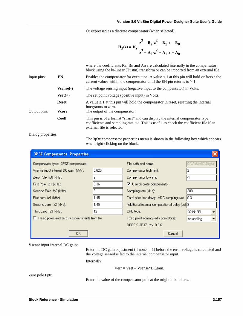
Version 8.0 VisSim Digital Power Designer Suite User’s Guide
Block Reference - Simulation 3.157
Or expressed as a discrete compensator (when selected):
where the coefficients Kz, Bn and An are calculated internally in the compensator
block using the bi-linear (Tustin) transform or can be imported from an external file.
Input pins: EN Enables the compensator for execution. A value < 1 at this pin will hold or freeze the
current values within the compensator until the EN pin returns to ≥ 1.
Vsense(-) The voltage sensing input (negative input to the compensator) in Volts.
Vset(+) The set point voltage (positive input) in Volts.
Reset A value ≥ 1 at this pin will hold the compensator in reset, resetting the internal
integrators to zero.
Output pins: Vcorr The output of the compensator.
Coeff This pin is of a format “struct” and can display the internal compensator type,
coefficients and sampling rate etc. This is useful to check the coefficient file if an
external file is selected.
Dialog properties:
The 3p3z compensator properties menu is shown in the following box which appears
when right-clicking on the block.
Vsense input internal DC gain:
Enter the DC gain adjustment (if none = 1) before the error voltage is calculated and
the voltage sensed is fed to the internal compensator input.
Internally:
Verr = Vset – Vsense*DCgain.
Zero pole Fp0:
Enter the value of the compensator pole at the origin in kilohertz.
H3 z( ) Kz
z3
B2 z2
B1 z B0
z3
A2 z2
A1 z A0
Version 8.0 VisSim Digital Power Designer Suite User’s Guide
3.158 Block Reference - Simulation
First pole Fp1:
Enter the value of the first pole of the compensator in kilohertz.
Second pole Fp2:
Enter the value of the second pole of the compensator in kilohertz
First zero Fz1:
Enter the value of the first zero of the compensator in kilohertz.
Second zero Fz2:
Enter the value of the second zero of the compensator in kilohertz.
Third zero Fz3:
Enter the value of the third zero of the compensator in kilohertz.
Read poles and zeros / z-coefficients from file:
Check this box if the compensator poles and zeros are to be read from a file. This file
can be typically generated by the compensator tools within the Tools section of the
digital power block set or by the control loop design tool.
Note that if a discrete compensator is NOT selected then the compensator block will
look for a poles and zeros format within the file. If a discrete compensator is selected
then the compensator block will look for a discrete coefficient format (z-coefficients)
within the file.
If an incorrect file is selected, the compensator block will signal an error at the start
of a simulation run and the block will turn red.
File path and name:
Enter the file name and path to the compensator coefficient file.
Compensator High limit:
Enter the high level limit of the compensator.
Compensator low limit:
Enter the low-level limit of the compensator.
NOTE that these limits are anti-windup limits.
Use discrete compensator:
Check this box if a discrete compensator is to be used in a simulation (digital
control).
Sampling rate:
Enter the discrete compensator sampling rate.
NOTE: If an external file is used for the discrete coefficients, the sampling rate used
to generate those coefficients must be equal to the value entered here. If the poles
and zeros are entered manually, the discrete compensator coefficients will be
automatically generated for the sample rate given here.
Total prior time delay – ADC sampling:
Enter any prior time delay (usually the sampling time of an ADC).
Additional internal computational delay:
Enter the additional time delay which would correspond to the time it takes for the
compensator to calculate its output value.
Version 8.0 VisSim Digital Power Designer Suite User’s Guide
Block Reference - Simulation 3.159
CPU type:
Enter the CPU type. The choices are:
1. Floating point (FPU) e.g. TI Delfino, Piccolo CLA
2. 16.bit fixed-point e.g TI TMS320F240x, MSP430
3. 32-bit fixed point e.g. TI piccolo A and piccolo B.
NOTE: If the compensator is to be simulated running in the CLA then the sampling
rate and entered time delay will reflect this and a FPU should be selected.
Fixed point scaling radix point:
Enter the fixed-point radix scaling in bits. The radix scaling is the number of bits
allocated to the whole number plus the sign bit.
Back
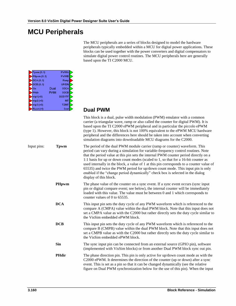
Version 8.0 VisSim Digital Power Designer Suite User’s Guide
3.160 Block Reference - Simulation
MCU Peripherals
The MCU peripherals are a series of blocks designed to model the hardware
peripherals typically embedded within a MCU for digital power applications. These
blocks can be used together with the power converters and digital compensators to
simulate digital power control routines. The MCU peripherals here are generally
based upon the TI C2000 MCU.
Dual PWM
This block is a dual, pulse width modulation (PWM) emulator with a common
carrier (a triangular wave, ramp or also called the counter for digital PWM). It is
based upon the TI C2000 ePWM peripheral and in particular the piccolo ePWM
(type 1). However, this block is not 100% equivalent to the ePWM MCU hardware
peripheral and the differences here should be taken into account when converting
simulation diagrams into downloadable MCU diagrams for the C2000.
Input pins: Tpwm The period of the dual PWM module carrier (ramp or counter) waveform. This
period can vary during a simulation for variable-frequency control routines. Note
that the period value at this pin sets the internal PWM counter period directly on a
1:1 basis for up or down count modes (scaled to 1, so that for a 16-bit counter as
used internally in the block, a value of 1 at this pin corresponds to a counter value of
65535) and twice the PWM period for up/down count mode. This input pin is only
enabled if the “change period dynamically” check box is selected in the dialog
display of this block.
PHpwm The phase value of the counter on a sync event. If a sync event occurs (sync input
pin or digital compare event; see below), the internal counter will be immediately
loaded with this value. The value must be between 0 and 1 which corresponds to
counter values of 0 to 65535.
DCA This input pin sets the duty cycle of any PWM waveform which is referenced to the
compare A (CMPA) value within the dual PWM block. Note that this input does not
set a CMPA value as with the C2000 but rather directly sets the duty cycle similar to
the VisSim embedded ePWM block.
DCB This input pin sets the duty cycle of any PWM waveform which is referenced to the
compare B (CMPB) value within the dual PWM block. Note that this input does not
set a CMPB value as with the C2000 but rather directly sets the duty cycle similar to
the VisSim embedded ePWM block.
Sin The sync input pin can be connected from an external source (GPIO pin), software
(implemented with VisSim blocks) or from another Dual PWM block sync out pin.
PHdir The phase direction pin. This pin is only active for up/down count mode as with the
C2000 ePWM. It determines the direction of the counter (up or down) after a sync
event. This is set as a pin so that it can be changed dynamically (see the relative
figure on Dual PWM synchronization below for the use of this pin). When the input

Version 8.0 VisSim Digital Power Designer Suite User’s Guide
Block Reference - Simulation 3.161
to this pin is ≥ 1, the counter will count UP after a synchronisation event, when the
input is < 1, the counter will count down after a synchronisation event.
Trip1 The trip inputs are similar to the trip zone (TZ) inputs on the C2000 ePWM. The trip
inputs can cause either PWMA or PWMB to be reset low or set high (the high
impedance option is not available), cause a sync event, send out a start of conversion
pulse for an ADC or cause a trip-zone interrupt TZINT. The tripping of the PWM
outputs can be cycle-by-cycle digital compare (CBC-DC) or cycle-by-cycle trip zone
(CBC-TZ) or one-shot digital compare (OS-DC) or one-shot trip zone (OS-TZ).
Refer to the relevant TI documentation for a more detailed description on the trip
zone module within the C2000 ePWM peripheral. The basic difference between a
CBC and a OS event as implemented here is that the CBC event is automatically
reset while a OS event must be reset by software (in this case at the reset input pin).
The basic difference between a DC CBC event and a TZ CBC event is that the DC
trip is reset immediately the event is no longer present (the input pin returns high)
while the TZ CBC trip is reset when the counter returns to zero. The trip input pins
are active low ( < 1).
Trip2 A second trip pin option.
Trip3 A third trip pin option.
Reset The reset pin enables a reset of the one-shot trip event. This is typically performed
by software in the C2000 MCU and can be performed in a simulation diagram using
standard VisSim blocks. When the input to this pin is ≥ 1, a reset of a OS trip event
will be performed, when the input is < 1, there will be no OS trip event reset. Note
that if a OS event is enabled, it may be necessary to hold the reset active at the start
of a simulation for a few simulation cycles to ensure that the Dual PWM block OS
event is not set on simulation start.
Output pins: PWMA The PWM output A.
PWMB The PWM output B.
Ramp The ramp pin output is analogous to the counter register on the C2000 except that it
is scaled from 0 to 1 for the graphical output representation. In this way, although the
internal counter operates similarly to the C2000, the amplitude of this output pin
does not vary with the counter period value.
UP/DN This output pin gives the current direction of the internal counter (1 = UP, 0 =
DOWN).
SOCA The Start Of Conversion A (SOCA) signal out to initiate a conversion of an ADC
block (If “Set SOC outputs as external GPIO output pins” is selected in the dialog
display below, on a SOC this output will be active low for 32 SYSCLKOUT (CPU
period) cycles, otherwise =1 for one time step only).
SOCB The Start Of Conversion B (SOCB) signal out to initiate a conversion of an ADC
block similar to SOCA.
DCEVTF This output allows the visualization of the filtered blanking window.
INT This output pin gives a high pulse (duration one simulation time step) according to
the selected interrupt output as given in the dialog display.
TZINT This output pin gives a high pulse (duration one simulation time step) according to
the selected interrupt trip input to be outputted as a trip-zone interrupt as given in the
dialog display.
Sout The sync out pin which can be connected up to other Dual PWM blocks in order to
synchronize their counters and eventually the PWM outputs.

Version 8.0 VisSim Digital Power Designer Suite User’s Guide
3.162 Block Reference - Simulation
Dialog properties:
The dual PWM block properties menu is shown in the following box which appears
when right-clicking on the block.
CPU clock rate SYSCLKOUT:
The CPU rate is set with this value in MHz. This value will affect the PWM
resolution and the internal timing and delays within the block.
Time base clock prescaling CLKDIV:
The counter pre-scaling and therefore the counter resolution can be set with this
value.
HSPCLK prescaling HSPCLKDIV:
Another option for pre-scaling of the PWM counter. This value is set to a default of 1
when code is generated for the VisSim ePWM embedded block.
Timer period TBPRD (1..65535):
Set the timer period and therefore the PWM frequency with this pin. The counter
frequency = SYSCLKOUT*CLKDIV*HSPCLKDIV/TBPRD for up count or down
count modes and the counter frequency =
SYSCLKOUT*CLKDIV*HSPCLKDIV/(2*TBPRD) for up/down count mode.

Version 8.0 VisSim Digital Power Designer Suite User’s Guide
Block Reference - Simulation 3.163
Change period dynamically:
If this box is checked, the above timer period value is ignored and the PWM period
is set using the input pin Tpwm.
Use high resolution PWM:
Check this box to enable high resolution of the ePWM generation. Since the C2000
ePWM high resolution is set around 150ps, this would require a simulation time step
of 75ps (or 13.3 GHz!) to represent it correctly and since such a time step would
rarely be used in a simulation, the high resolution PWM rate is limited to the
simulation time step for time steps greater than 150ps. The high resolution option is
implemented by changing the resolution of the carrier (counter) waveform. This
varies from the technique used for the C2000 which uses a proprietary Micro Edge
Positioner (MEP). See the relevant TI documentation for details.
Carrier (counter) type:
The choices here are (see the figure below):
1. Up count
2. Down count
3. Up / down count
PWMA output high at counter:
Select the counter value at which the PWMA output is set to high (=1). The choices
are:
1. Zero – The counter equals zero.
2. Period – The counter equals the maximum set value (the output pin ramp =
1).
3. CMPA up – The counter reaches the DCA input value on the UP count (not
available for down count configuration).
4. CMPA down – The counter reaches the DCA input value on the DOWN
count (not available for up count configuration).

Version 8.0 VisSim Digital Power Designer Suite User’s Guide
3.164 Block Reference - Simulation
5. CMPB up – The counter reaches the DCB input value on the UP count (not
available for down count configuration).
6. CMPB down – The counter reaches the DCB input value on the DOWN
count (not available for up count configuration).
7. Never – no action is taken.
PWMA output low at counter:
The choices and actions are the same as in PWMA output high above except that the
PWM output will be reset to zero on the selected event.
Toggle PWMA output at counter:
The choices and actions are the same as in PWMA output high above except that the
PWMA output will be toggled (the output will change its state) on the selected event.
PWMB output high at counter:
The choices and actions are the same as in PWMA output high above except that the
PWMB output will be set to high (=1) on the selected event.
PWMB output low at counter:
The choices and actions are the same as in PWMA output high above except that the
PWMB output will be reset to zero on the selected event.
Toggle PWMB output at counter:
The choices and actions are the same as in PWMB output high above except that the
PWMB output will be toggled (the output will change its state) on the selected event.
Note that with this block configuration, only one event can be chosen for each type
of action on a particular PWM output. In the C2000 ePWM (as in the VisSim
embedded ePWM block), any number of the available events can be assigned to a
particular PWM action.
Apply dead time:
Check this box to apply a dead time between the two PWM outputs. This dead time
can be configured in many different ways by setting the following options. This
section emulates directly the dead-band generator sub-module in the C2000 ePWM
(type 1) peripheral. For further information, refer to the relative TI documentation.
Input mode:
Select the scope of the dead time on the two PWM outputs. The choices are:
1. PWMA into FED and RED (default)
2. PWMB into RED, PWMA into FED
3. PWMB into FED, PWMA into RED
4. PWMB into FED and RED.
Polarity:
Select the polarity of the dead-time from the following:
1. Active high
2. Active low complementary
3. Active high complementary
4. Active low
These configurations are shown in the figure below.
Rising edge delay:
Enter the desired value of the rising edge delay in nanoseconds
Falling edge delay:
Enter the desired value of the falling edge delay in nanoseconds.
Note that although the delays are entered in nanoseconds, the delays are discretized
at 10 bit resolution emulating the C2000 type 1 ePWM dead-time module.
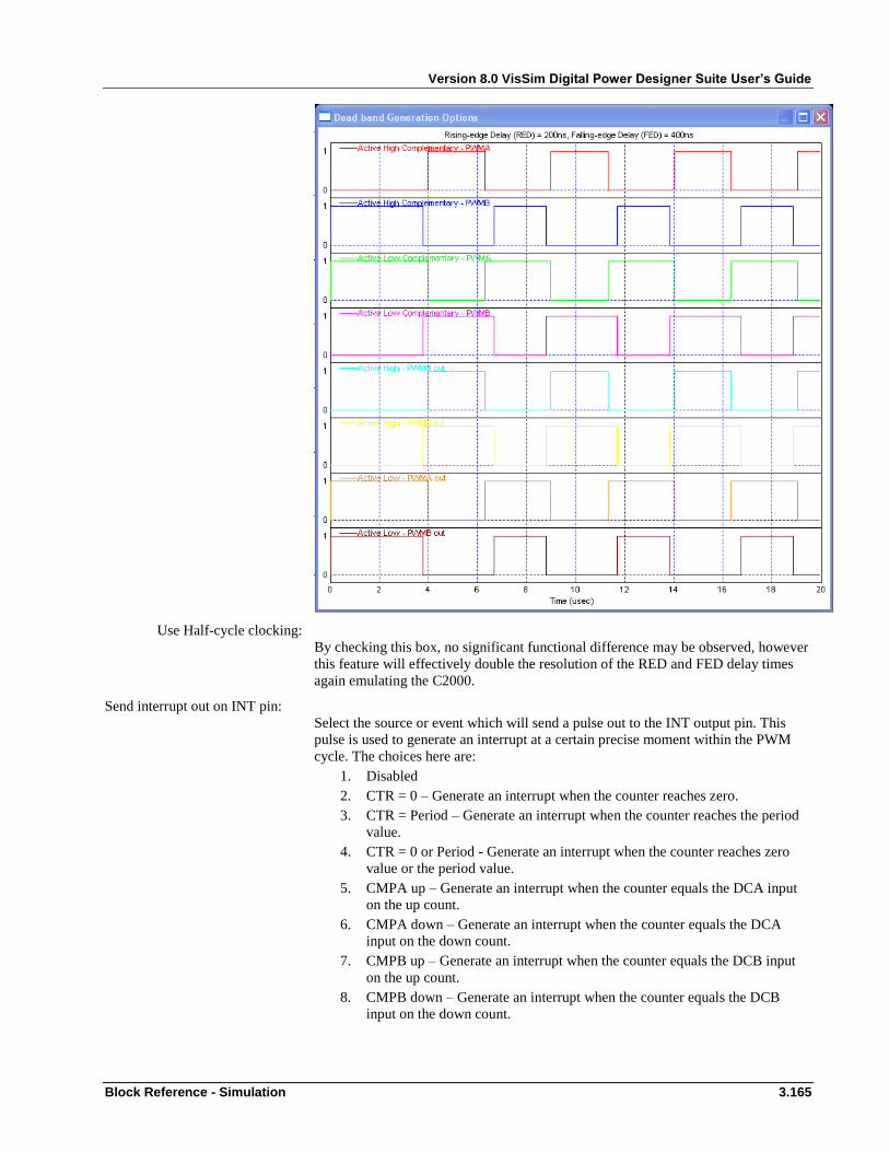
Version 8.0 VisSim Digital Power Designer Suite User’s Guide
Block Reference - Simulation 3.165
Use Half-cycle clocking:
By checking this box, no significant functional difference may be observed, however
this feature will effectively double the resolution of the RED and FED delay times
again emulating the C2000.
Send interrupt out on INT pin:
Select the source or event which will send a pulse out to the INT output pin. This
pulse is used to generate an interrupt at a certain precise moment within the PWM
cycle. The choices here are:
1. Disabled
2. CTR = 0 – Generate an interrupt when the counter reaches zero.
3. CTR = Period – Generate an interrupt when the counter reaches the period
value.
4. CTR = 0 or Period - Generate an interrupt when the counter reaches zero
value or the period value.
5. CMPA up – Generate an interrupt when the counter equals the DCA input
on the up count.
6. CMPA down – Generate an interrupt when the counter equals the DCA
input on the down count.
7. CMPB up – Generate an interrupt when the counter equals the DCB input
on the up count.
8. CMPB down – Generate an interrupt when the counter equals the DCB
input on the down count.
Version 8.0 VisSim Digital Power Designer Suite User’s Guide
3.166 Block Reference - Simulation
Send interrupt pulse out on:
Here the choices are:
1. Never
2. Every event
3. Every 2nd event
4. Every 3rd event
The output pin will normally be low (zero) and go high (=1) for one simulation time
step on the selected interrupt event.
Send SOCA on:
Select the source or event which will send a pulse out to the SOCA output pin. This
pulse is used to send a Start Of Conversion to an analog-to-digital converter (ADC).
The choices here are:
1. Never
2. CTR = 0 – Send a SOC when the counter reaches zero.
3. CTR = Period – Send a SOC when the counter reaches the period value.
4. CTR = 0 or Period – Send a SOC when the counter reaches the period
value.
5. CMPA up – Send a SOC when the counter equals the DCA input on the up
count.
6. CMPA down – Send a SOC when the counter equals the DCA input on the
down count.
7. CMPB up – Send a SOC when the counter equals the DCB input on the up
count.
8. CMPB down – Send a SOC when the counter equals the DCB input on the
down count.
9. Trip 1 – Send a SOC when a trip 1 event occurs (only applicable when
configured as a digital compare).
10. Trip 2 1 – Send a SOC when a trip 2 event occurs (only applicable when
configured as a digital compare).
11. Trip 3 1 – Send a SOC when a trip 3 event occurs (only applicable when
configured as a digital compare).
Send SOCA pulse out on:
Here the choices are:
1. Never
2. Every event
3. Every 2nd event
4. Every 3rd event
Send SOCB on:
Select the source or event at which a pulse is sent at the SOCB output pin. The
selection and actions are the same as for SOCA.
Send SOCB pulse out on:
The selection here is the same as for SOCA.
Set SOC outputs as external GPIO output pins.:
If the check box is selected then the SOC output will be active low. i.e. they will
normally be high (=1) and go low (=0) on the selected SOC event for 32
SYSCLKOUT cycles. Otherwise, if unchecked, the SOC output pins will normally
be low and go high for one simulation time step on the selected SOC event.
Synchronize counter to pulse on:
Set the event on which to synchronise the counter. The choices are:
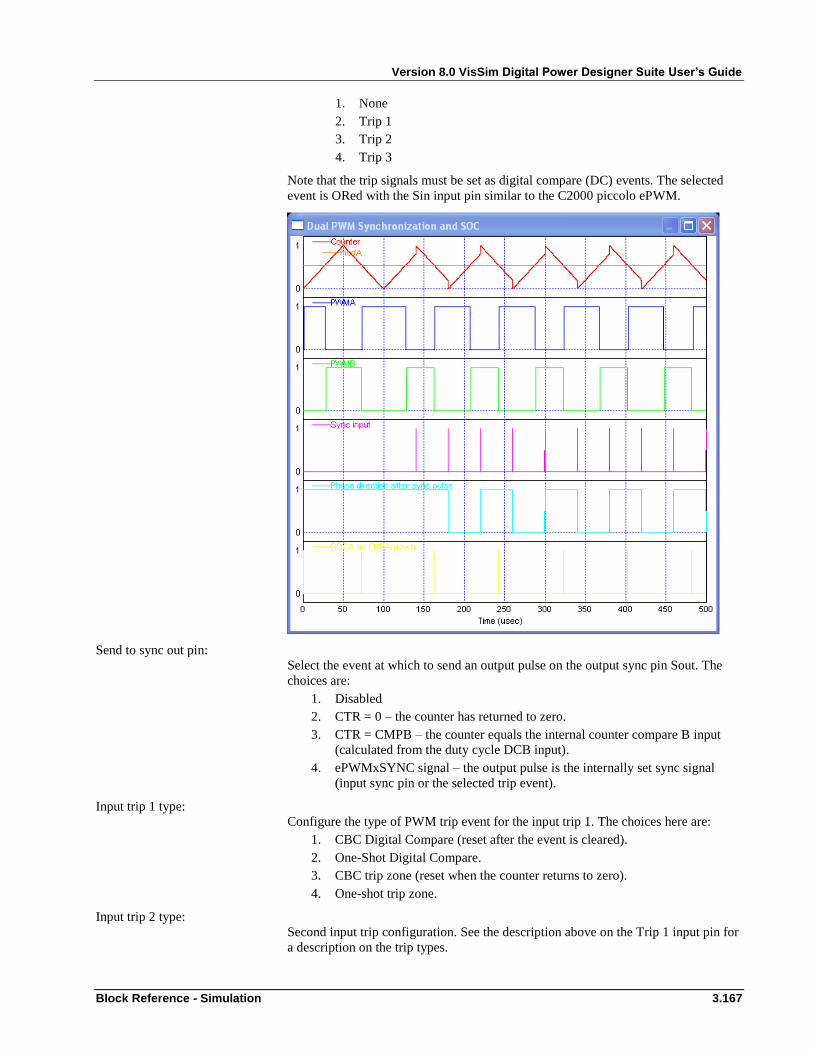
Version 8.0 VisSim Digital Power Designer Suite User’s Guide
Block Reference - Simulation 3.167
1. None
2. Trip 1
3. Trip 2
4. Trip 3
Note that the trip signals must be set as digital compare (DC) events. The selected
event is ORed with the Sin input pin similar to the C2000 piccolo ePWM.
Send to sync out pin:
Select the event at which to send an output pulse on the output sync pin Sout. The
choices are:
1. Disabled
2. CTR = 0 – the counter has returned to zero.
3. CTR = CMPB – the counter equals the internal counter compare B input
(calculated from the duty cycle DCB input).
4. ePWMxSYNC signal – the output pulse is the internally set sync signal
(input sync pin or the selected trip event).
Input trip 1 type:
Configure the type of PWM trip event for the input trip 1. The choices here are:
1. CBC Digital Compare (reset after the event is cleared).
2. One-Shot Digital Compare.
3. CBC trip zone (reset when the counter returns to zero).
4. One-shot trip zone.
Input trip 2 type:
Second input trip configuration. See the description above on the Trip 1 input pin for
a description on the trip types.

Version 8.0 VisSim Digital Power Designer Suite User’s Guide
3.168 Block Reference - Simulation
Input trip 3 type:
Third input trip configuration. See the description above on the Trip 1 input pin for a
description on the trip types.
Scope of input trip 1 on PWMA:
Configure the action taken on the PWMA output on a trip 1 event. The choices here
are:
1. Disabled
2. Force low
3. Force high
Note that a high impedance output option is not available.
Scope of input trip 2 on PWMA:
Configure the action taken on the PWMA output on a trip 2 event.
Scope of input trip 3 on PWMA:
Configure the action taken on the PWMA output on a trip 3 event.
Scope of input trip 1 on PWMB:
Configure the action taken on the PWMB output on a trip 1 event.
Scope of input trip 2 on PWMB:
Configure the action taken on the PWMB output on a trip 2 event.
Scope of input trip 3 on PWMB:
Configure the action taken on the PWMB output on a trip 3 event.
Send TZ interrupt out on TZINT pin:
This selection will allow a trip interrupt pulse to be sent out on the TZINT pin. The
choices are:
1. Disabled
2. Trip 1 – only generated on a digital compare event.
3. Trip 2 – only generated on a digital compare event.
4. Trip 3 – only generated on a digital compare event.
5. CBC trip event – generated on any cycle-by-cycle event.
6. OS trip event – generated on any one-shot event.
Include leading edge blanking:
Check this box to include a blanking window (filter) on the selected trip event.
Filter (apply blanking) to trip event:
Leading-edge blanking (LEB) is normally applied to a trip signal in order to filter
that signal or more precisely “ignore” it for a given window of time. This is useful to
filter out any noise impulses during the switching instant of power semiconductor
devices.
Select the source for the filtered signal for blanking. The choices are:
1. Trip 1 input
2. Trip 2 input
3. Trip 3 input
4. PWMA trip
5. PWMB trip
Note that this selection varies from the blanking configuration of the TI C2000
ePWM leading-edge blanking (LEB) configuration. Please refer to the appropriate TI
documentation. In this block, either one of the trip inputs or the actual trip on the
PWM output can be blanked.

Version 8.0 VisSim Digital Power Designer Suite User’s Guide
Block Reference - Simulation 3.169
Align blanking window to:
The blanking window can be aligned to:
1. CTR = 0
2. CTR = period.
Blanking window delay:
Enter the delay time at which the blanking window commences (aligned as above),
in nanoseconds.
Blanking window:
Enter the width of the blanking window in nanoseconds.
Note that although the blanking time delay and window are given in nanoseconds,
the times are discretized to emulate the C2000 blanking time sub-module.
Invert blanking window:
Select this box to invert (phase shift) the blanking window.
Back
eCAP-PWM
This block is based upon the TI C2000 eCAP peripheral sub-module for
Asynchronous PWM.
Input Pins: DC The duty cycle input from 0 to 1. Note that this is not a compare value input.
Period The value at this pin will set the period value of the PWM carrier (Up counter). The
input value is the value of the 32-bit counter scaled from 0 to 1.
Phase The value at this pin will set the phase value of the PWM carrier. The input value is
the value of the 32-bit counter scaled from 0 to 1. The counter will be set to this
value at the instant that the input Sin pin goes high.
Sin Input pin to synchronize the counter with other eCAP modules or PWM modules.
Output pins: PWM The PWM output.
ramp The internal counter value scaled from 0 to 1 for all periods.
INT Interrupt output pin (active high for one simulation time step).
Sout Synch output pin (active high for one simulation time step).
Dialog properties:
The eCAP-PWM block properties menu is shown in the following box which
appears when right-clicking on the block.
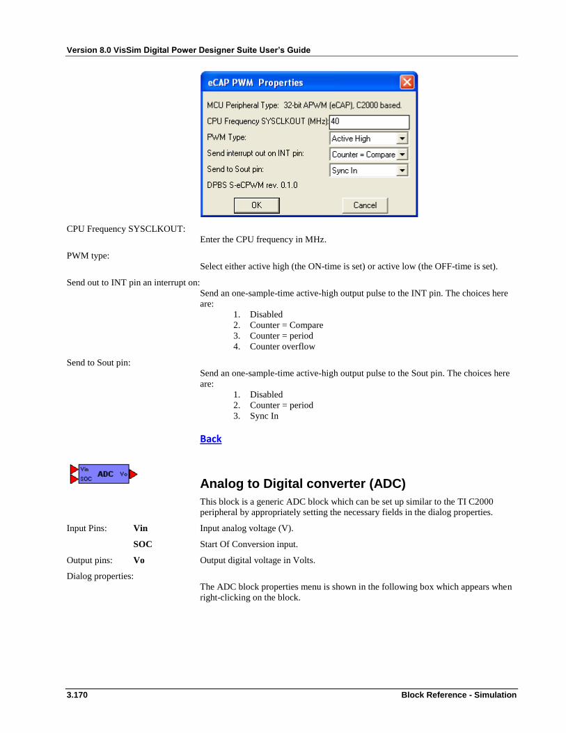
Version 8.0 VisSim Digital Power Designer Suite User’s Guide
3.170 Block Reference - Simulation
CPU Frequency SYSCLKOUT:
Enter the CPU frequency in MHz.
PWM type:
Select either active high (the ON-time is set) or active low (the OFF-time is set).
Send out to INT pin an interrupt on:
Send an one-sample-time active-high output pulse to the INT pin. The choices here
are:
1. Disabled
2. Counter = Compare
3. Counter = period
4. Counter overflow
Send to Sout pin:
Send an one-sample-time active-high output pulse to the Sout pin. The choices here
are:
1. Disabled
2. Counter = period
3. Sync In
Back
Analog to Digital converter (ADC)
This block is a generic ADC block which can be set up similar to the TI C2000
peripheral by appropriately setting the necessary fields in the dialog properties.
Input Pins: Vin Input analog voltage (V).
SOC Start Of Conversion input.
Output pins: Vo Output digital voltage in Volts.
Dialog properties:
The ADC block properties menu is shown in the following box which appears when
right-clicking on the block.
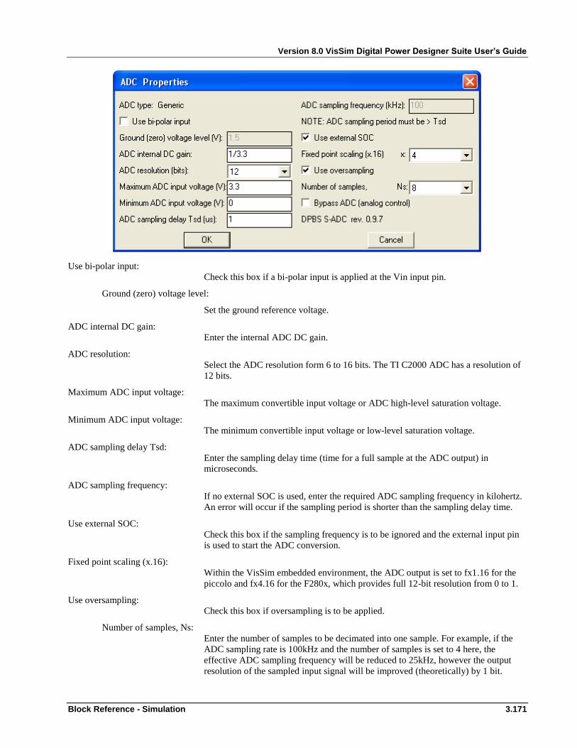
Version 8.0 VisSim Digital Power Designer Suite User’s Guide
Block Reference - Simulation 3.171
Use bi-polar input:
Check this box if a bi-polar input is applied at the Vin input pin.
Ground (zero) voltage level:
Set the ground reference voltage.
ADC internal DC gain:
Enter the internal ADC DC gain.
ADC resolution:
Select the ADC resolution form 6 to 16 bits. The TI C2000 ADC has a resolution of
12 bits.
Maximum ADC input voltage:
The maximum convertible input voltage or ADC high-level saturation voltage.
Minimum ADC input voltage:
The minimum convertible input voltage or low-level saturation voltage.
ADC sampling delay Tsd:
Enter the sampling delay time (time for a full sample at the ADC output) in
microseconds.
ADC sampling frequency:
If no external SOC is used, enter the required ADC sampling frequency in kilohertz.
An error will occur if the sampling period is shorter than the sampling delay time.
Use external SOC:
Check this box if the sampling frequency is to be ignored and the external input pin
is used to start the ADC conversion.
Fixed point scaling (x.16):
Within the VisSim embedded environment, the ADC output is set to fx1.16 for the
piccolo and fx4.16 for the F280x, which provides full 12-bit resolution from 0 to 1.
Use oversampling:
Check this box if oversampling is to be applied.
Number of samples, Ns:
Enter the number of samples to be decimated into one sample. For example, if the
ADC sampling rate is 100kHz and the number of samples is set to 4 here, the
effective ADC sampling frequency will be reduced to 25kHz, however the output
resolution of the sampled input signal will be improved (theoretically) by 1 bit.
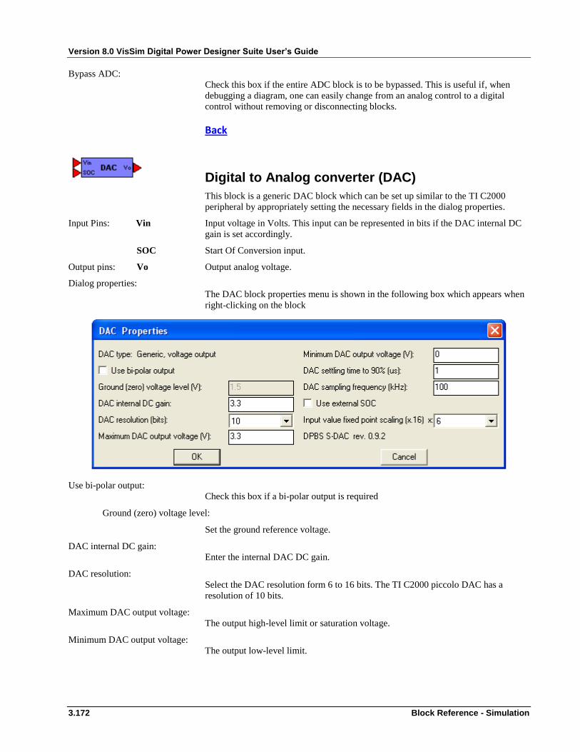
Version 8.0 VisSim Digital Power Designer Suite User’s Guide
3.172 Block Reference - Simulation
Bypass ADC:
Check this box if the entire ADC block is to be bypassed. This is useful if, when
debugging a diagram, one can easily change from an analog control to a digital
control without removing or disconnecting blocks.
Back
Digital to Analog converter (DAC)
This block is a generic DAC block which can be set up similar to the TI C2000
peripheral by appropriately setting the necessary fields in the dialog properties.
Input Pins: Vin Input voltage in Volts. This input can be represented in bits if the DAC internal DC
gain is set accordingly.
SOC Start Of Conversion input.
Output pins: Vo Output analog voltage.
Dialog properties:
The DAC block properties menu is shown in the following box which appears when
right-clicking on the block
Use bi-polar output:
Check this box if a bi-polar output is required
Ground (zero) voltage level:
Set the ground reference voltage.
DAC internal DC gain:
Enter the internal DAC DC gain.
DAC resolution:
Select the DAC resolution form 6 to 16 bits. The TI C2000 piccolo DAC has a
resolution of 10 bits.
Maximum DAC output voltage:
The output high-level limit or saturation voltage.
Minimum DAC output voltage:
The output low-level limit.
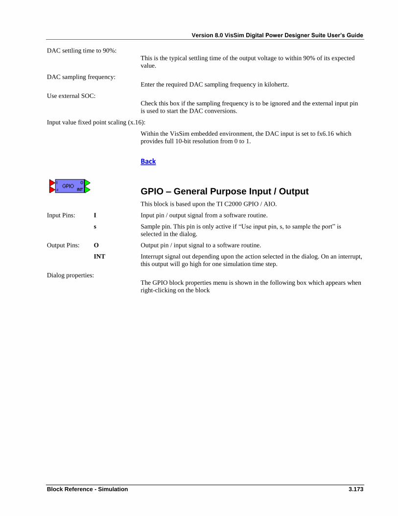
Version 8.0 VisSim Digital Power Designer Suite User’s Guide
Block Reference - Simulation 3.173
DAC settling time to 90%:
This is the typical settling time of the output voltage to within 90% of its expected
value.
DAC sampling frequency:
Enter the required DAC sampling frequency in kilohertz.
Use external SOC:
Check this box if the sampling frequency is to be ignored and the external input pin
is used to start the DAC conversions.
Input value fixed point scaling (x.16):
Within the VisSim embedded environment, the DAC input is set to fx6.16 which
provides full 10-bit resolution from 0 to 1.
Back
GPIO – General Purpose Input / Output
This block is based upon the TI C2000 GPIO / AIO.
Input Pins: I Input pin / output signal from a software routine.
s Sample pin. This pin is only active if “Use input pin, s, to sample the port” is
selected in the dialog.
Output Pins: O Output pin / input signal to a software routine.
INT Interrupt signal out depending upon the action selected in the dialog. On an interrupt,
this output will go high for one simulation time step.
Dialog properties:
The GPIO block properties menu is shown in the following box which appears when
right-clicking on the block
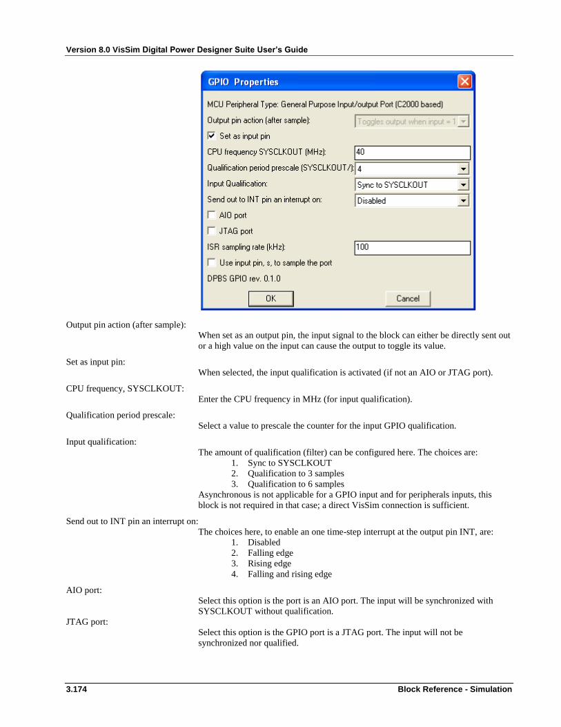
Version 8.0 VisSim Digital Power Designer Suite User’s Guide
3.174 Block Reference - Simulation
Output pin action (after sample):
When set as an output pin, the input signal to the block can either be directly sent out
or a high value on the input can cause the output to toggle its value.
Set as input pin:
When selected, the input qualification is activated (if not an AIO or JTAG port).
CPU frequency, SYSCLKOUT:
Enter the CPU frequency in MHz (for input qualification).
Qualification period prescale:
Select a value to prescale the counter for the input GPIO qualification.
Input qualification:
The amount of qualification (filter) can be configured here. The choices are:
1. Sync to SYSCLKOUT
2. Qualification to 3 samples
3. Qualification to 6 samples
Asynchronous is not applicable for a GPIO input and for peripherals inputs, this
block is not required in that case; a direct VisSim connection is sufficient.
Send out to INT pin an interrupt on:
The choices here, to enable an one time-step interrupt at the output pin INT, are:
1. Disabled
2. Falling edge
3. Rising edge
4. Falling and rising edge
AIO port:
Select this option is the port is an AIO port. The input will be synchronized with
SYSCLKOUT without qualification.
JTAG port:
Select this option is the GPIO port is a JTAG port. The input will not be
synchronized nor qualified.

Version 8.0 VisSim Digital Power Designer Suite User’s Guide
Block Reference - Simulation 3.175
ISR sampling rate (kHz):
The GPIO port (either input or output) will be sampled at this rate. Enter the value of
the sampling rate where the port will be placed in a code-generable diagram.
Use input pin, s, to sample the port:
Select this option if the port is to be sampled by an external signal. In this case, the
precise moment of the port sampling instant can be modelled.
Back
Event Capture (CAP)
This block is based upon the TI C2000 eCAP peripheral.
Input Pins:
CTRen Counter enable pin; if this pin goes low, the counter will be frozen at the current
value.
Vin Input signal to be captured.
Phase(0..1) Phase value of the 32-bit counter scaled from 0 to 1. This value will be set if a sync
signal is present at the Sin pin.
Sin Sync input signal. This pin can be used to synchronize several CAP block timers to
synchronise the CAP timer with a PWM block.
R Input reset applicable for one-shot mode.
Output Pins: E1 Counter value on Event 1
E2 Counter value on Event 2
E3 Counter value on Event 3
E4 Counter value on Event 4
INT Interrupt signal out depending upon the event selection in the dialog. On an interrupt,
this output will go high for one simulation time step.
Sout Sync signal output pin to be connected to other CAP blocks.
Dialog properties:
The CAP block properties menu is shown in the following box which appears when
right-clicking on the block

Version 8.0 VisSim Digital Power Designer Suite User’s Guide
3.176 Block Reference - Simulation
CPU frequency SYSCLKOUT:
Enter the value of the 32-bit counter frequency. The higher the frequency, the more
accurate the result however the smaller the simulation time step required. The value
is typically the MCU rate, however lower values can be applied in order to speed up
the simulation.
Input event prescale:
The input signal can be prescaled or rather, the frequency of the input signal is
frequency divided.
Event x Trigger on:
Each event can be set up to trigger either on the rising or the falling edge.
Number of events:
This is applicable for wrap-around mode. Select the maximum number of events
required. After the specified number of events, the captures will “wrap-around” to
the first event and repeat.
Enable one-shot mode:
Check this checkbox if one-shot mode is required. In this mode the captures will stop
after the specified event. It can be reset using the R(OS) input pin.
Stop after capture event:
Select the event on which the captures should stop (values frozen).
Send out to INT pin an interrupt on:
Send a one simulation-time-step, active-high output pulse to the INT pin. The
choices here are:
1. Disabled
2. Event 1
3. Event 2
4. Event 3
5. Event 4
6. Counter overflow

Version 8.0 VisSim Digital Power Designer Suite User’s Guide
Block Reference - Simulation 3.177
Send to Sout pin:
Send an one simulation-time-step, active-high output pulse to the Sout pin. The
choices here are:
1. Disabled
2. Sync In
Reset counter on event x:
When selected, the counter will be reset on this event. Multiple events can be
selected for reset.
Back
Analog comparator
The analog comparator can be used in a simulation as a typical analog comparator or
as an embedded comparator found in a MCU such as that of the TI piccolo MCU.
Input Pins: Vin(+) Input voltage (V) – positive input pin.
Vref(-) Reference voltage (V) – negative input pin (only active if the external reference is
selected).
Output pins: Vo Output = 1 if Vin > Vref and hysteresis = none.
= 0 if Vin < Vref and hysteresis = none.
If hysteresis is defined then the output will also depend upon this value and its
polarity.
RR Reset Ramp. This pin is always subject to the selected qualification and is normally
used to reset the ramp generator back to its maximum value after a comparator
output change.
Dialog properties:
The Comparator block properties menu is shown in the following box which appears
when right-clicking on the block
Version 8.0 VisSim Digital Power Designer Suite User’s Guide
3.178 Block Reference - Simulation
Reference voltage:
Enter the value of the voltage, in Volts, at the reference pin.
Use external reference pin:
If checked, the reference voltage above will be ignored and the input pin Vref(+) will
be taken as the reference voltage.
Hysteresis level:
Enter the value of the hysteresis in Volts. For the C2000 piccolo comparators this is
typically 35mV.
Apply hysteresis to:
An hysteresis voltage can be applied according to the following selection:
1. None
2. output H -> L transition only.
3. output L -> H transition only.
4. Dual polarity.
Note that this selection varies from the C2000 peripheral where in that case the
hysteresis is fixed in hardware.
Invert output:
The output will be inverted when this box is checked.
CPU frequency, SYSCLKOUT:
Enter the frequency of the CPU clocking.
Output qualification, SYSCLKOUT cycles:
Enter the number of CPU clock cycles that will determine the duration of the
filtering of the comparator trip output. Note that this filter will always be active on
the comparator reset ramp (RR) output.
Include qualification on comparator output:
The output qualification will be included on the comparator output when this box is
checked.
Back

Version 8.0 VisSim Digital Power Designer Suite User’s Guide
Block Reference - Simulation 3.179
Ramp Generator
The ramp generator block emulates the ramp generator in the comparator-DAC block
of the TI C2000.
Input Pins: Mval(0..1) This pin sets the maximum value or reset value of the ramp in 10 bit resolution,
scaled from 0 to 1.
Dval(0..1) This pin sets the decrement value of the ramp in 10 bit resolution, scaled from 0 to 1.
Sync Input sync pin to synchronise the ramp with a PWM output – connect from a Dual
PWM sync output pin.
Reset A reset input to reset the ramp back to its maximum value (Mval).
Output pins: Ramp(1..0) The output ramp.
SOC A start of conversion pulse which can be connected to the SOC input of a DAC
block.
Sample rate (SYSCLKOUT):
Set the sample rate of the ramp generator at the CPU frequency. The ramp is
decremented according to the most significant 10 bits of a 16 bit counter and is
therefore decremented at a rate of SYSCLKOUT/64.
Back
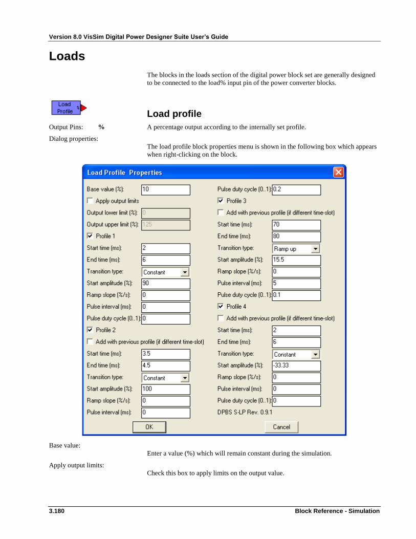
Version 8.0 VisSim Digital Power Designer Suite User’s Guide
3.180 Block Reference - Simulation
Loads
The blocks in the loads section of the digital power block set are generally designed
to be connected to the load% input pin of the power converter blocks.
Load profile
Output Pins: % A percentage output according to the internally set profile.
Dialog properties:
The load profile block properties menu is shown in the following box which appears
when right-clicking on the block.
Base value:
Enter a value (%) which will remain constant during the simulation.
Apply output limits:
Check this box to apply limits on the output value.
Version 8.0 VisSim Digital Power Designer Suite User’s Guide
Block Reference - Simulation 3.181
Output lower and upper limit:
Enter the required limiting values in %.
Profile x:
Check each profile to enable a different time slot and / or transition.
Start time:
Enter the start time of each profile in milliseconds.
End time:
Enter the stop time of each profile in milliseconds.
Transition type:
There are four choices here:
1. Constant
2. Ramp up
3. Ramp down
4. Pulses
Start amplitude:
The amplitude in % at the start of the profile.
Ramp slope:
When a ramp is selected as a transition, enter the slope of the ramp in %/s.
Pulse interval:
When pulses are selected, enter the pulse interval (period) in milliseconds.
Pulse duty cycle:
Enter the duty cycle of the pulses (when selected).
Add with previous profile:
If the profile has an overlapping time slot, it will automatically be added to the other
profile(s) with that time slot. If the time slots are not overlapping, the corresponding
profile can be summed with the previous profile by checking this box.
Back
Multi-load Profile
This block can be connected to the Load% input pin of the power converters for load
profiles of converters with up to 4 different outputs.
Output Pin: %(1..4) A percentage output according to the internally set profiles, vector (rows = 1,
columns = 4).
Dialog properties:
The multi-load profile block properties menu is shown in the following box which
appears when right-clicking on the block.

Version 8.0 VisSim Digital Power Designer Suite User’s Guide
3.182 Block Reference - Simulation
The fields are the same as for the load profile block accept that only one profile can
be applied per converter output.
Back
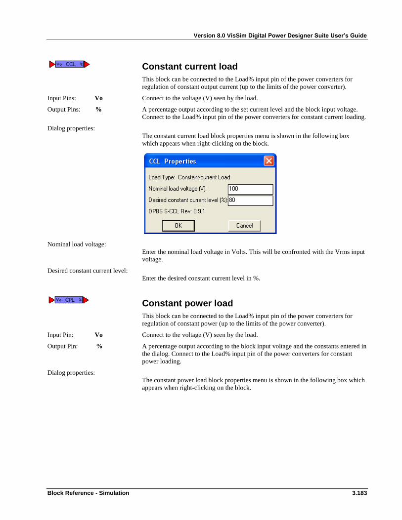
Version 8.0 VisSim Digital Power Designer Suite User’s Guide
Block Reference - Simulation 3.183
Constant current load
This block can be connected to the Load% input pin of the power converters for
regulation of constant output current (up to the limits of the power converter).
Input Pins: Vo Connect to the voltage (V) seen by the load.
Output Pins: % A percentage output according to the set current level and the block input voltage.
Connect to the Load% input pin of the power converters for constant current loading.
Dialog properties:
The constant current load block properties menu is shown in the following box
which appears when right-clicking on the block.
Nominal load voltage:
Enter the nominal load voltage in Volts. This will be confronted with the Vrms input
voltage.
Desired constant current level:
Enter the desired constant current level in %.
Constant power load
This block can be connected to the Load% input pin of the power converters for
regulation of constant power (up to the limits of the power converter).
Input Pin: Vo Connect to the voltage (V) seen by the load.
Output Pin: % A percentage output according to the block input voltage and the constants entered in
the dialog. Connect to the Load% input pin of the power converters for constant
power loading.
Dialog properties:
The constant power load block properties menu is shown in the following box which
appears when right-clicking on the block.
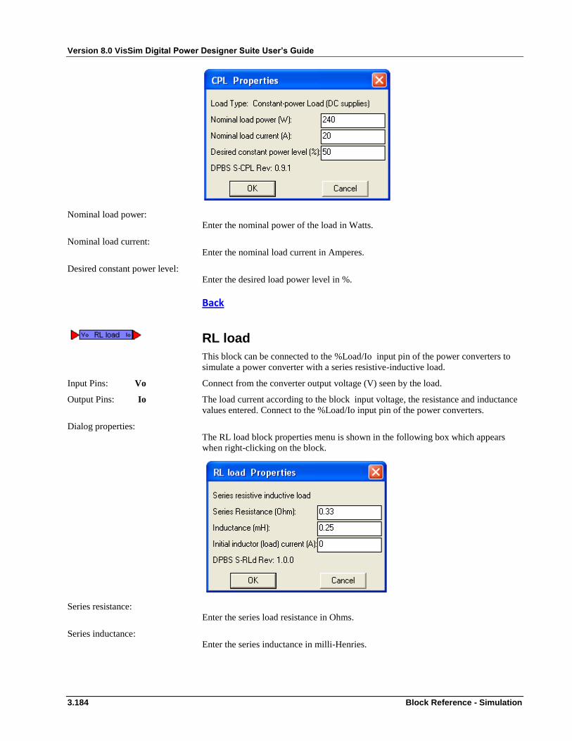
Version 8.0 VisSim Digital Power Designer Suite User’s Guide
3.184 Block Reference - Simulation
Nominal load power:
Enter the nominal power of the load in Watts.
Nominal load current:
Enter the nominal load current in Amperes.
Desired constant power level:
Enter the desired load power level in %.
Back
RL load
This block can be connected to the %Load/Io input pin of the power converters to
simulate a power converter with a series resistive-inductive load.
Input Pins: Vo Connect from the converter output voltage (V) seen by the load.
Output Pins: Io The load current according to the block input voltage, the resistance and inductance
values entered. Connect to the %Load/Io input pin of the power converters.
Dialog properties:
The RL load block properties menu is shown in the following box which appears
when right-clicking on the block.
Series resistance:
Enter the series load resistance in Ohms.
Series inductance:
Enter the series inductance in milli-Henries.
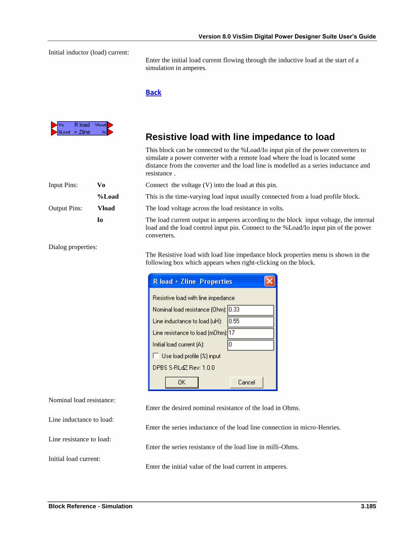
Version 8.0 VisSim Digital Power Designer Suite User’s Guide
Block Reference - Simulation 3.185
Initial inductor (load) current:
Enter the initial load current flowing through the inductive load at the start of a
simulation in amperes.
Back
Resistive load with line impedance to load
This block can be connected to the %Load/Io input pin of the power converters to
simulate a power converter with a remote load where the load is located some
distance from the converter and the load line is modelled as a series inductance and
resistance .
Input Pins: Vo Connect the voltage (V) into the load at this pin.
%Load This is the time-varying load input usually connected from a load profile block.
Output Pins: Vload The load voltage across the load resistance in volts.
Io The load current output in amperes according to the block input voltage, the internal
load and the load control input pin. Connect to the %Load/Io input pin of the power
converters.
Dialog properties:
The Resistive load with load line impedance block properties menu is shown in the
following box which appears when right-clicking on the block.
Nominal load resistance:
Enter the desired nominal resistance of the load in Ohms.
Line inductance to load:
Enter the series inductance of the load line connection in micro-Henries.
Line resistance to load:
Enter the series resistance of the load line in milli-Ohms.
Initial load current:
Enter the initial value of the load current in amperes.
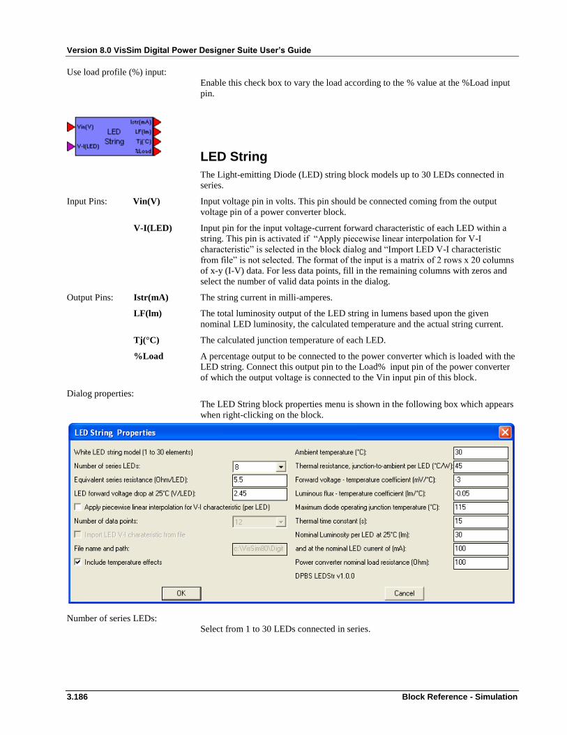
Version 8.0 VisSim Digital Power Designer Suite User’s Guide
3.186 Block Reference - Simulation
Use load profile (%) input:
Enable this check box to vary the load according to the % value at the %Load input
pin.
LED String
The Light-emitting Diode (LED) string block models up to 30 LEDs connected in
series.
Input Pins: Vin(V) Input voltage pin in volts. This pin should be connected coming from the output
voltage pin of a power converter block.
V-I(LED) Input pin for the input voltage-current forward characteristic of each LED within a
string. This pin is activated if “Apply piecewise linear interpolation for V-I
characteristic” is selected in the block dialog and “Import LED V-I characteristic
from file” is not selected. The format of the input is a matrix of 2 rows x 20 columns
of x-y (I-V) data. For less data points, fill in the remaining columns with zeros and
select the number of valid data points in the dialog.
Output Pins: Istr(mA) The string current in milli-amperes.
LF(lm) The total luminosity output of the LED string in lumens based upon the given
nominal LED luminosity, the calculated temperature and the actual string current.
Tj(°C) The calculated junction temperature of each LED.
%Load A percentage output to be connected to the power converter which is loaded with the
LED string. Connect this output pin to the Load% input pin of the power converter
of which the output voltage is connected to the Vin input pin of this block.
Dialog properties:
The LED String block properties menu is shown in the following box which appears
when right-clicking on the block.
Number of series LEDs:
Select from 1 to 30 LEDs connected in series.

Version 8.0 VisSim Digital Power Designer Suite User’s Guide
Block Reference - Simulation 3.187
Equivalent series resistance:
For the simple LED model, enter the value of the equivalent series resistance of each
LED in Ohms.
LED forward voltage drop at 25°C (V/LED):
Again for the simple LED model, enter the value of the LED forward voltage drop in
Volts.
Apply piecewise linear interpolation for V-I characteristic:
A piece-wise linear approximation can be applied to the LED curve in order to
achieve a more accurate representation of the LED V-I characteristic.
Number of data points:
Enter the number of data points to be used within the model from 2 to 20.
Import LED V-I characteristic from file:
If the piecewise linear model is selected and this box is checked, the LED string
block will use the specified data file. Otherwise the input V-I pin will be used for the
V-I characteristic. The file and the matrix at the input pin should be 2 rows x 20
columns. If less data points are required, the file or matrix should be filled with zeros
and the number of points in the model can be selected as above.
File path and name:
Enter the file name and path of the LED V-I characteristic data file.
Include temperature effects:
Select this if the LED temperature is to be considered within the model (applies to
both the simple linear and the piece-wise linear models).
Ambient temperature (°C):
Enter the expected ambient temperature around the LED string in degrees centigrade.
Thermal resistance, junction-to-ambient per LED (°C/W):
Enter the value of the junction to ambient thermal resistance of each LED. This
would be the sum of the junction to pad (case) thermal resistance, the pad to
copper/FR4 printed circuit thermal resistance and the printed circuit to ambient
thermal resistance.
Forward voltage temperature coefficient (mV/°C):
Enter the value of the rate at which the LED forward voltage (per LED) decreases
with increasing temperature. This value would normally be negative as the forward
voltage tends to decrease with temperature. This characteristic is assumed to be
linear.
Luminous flux temperature coefficient (lm/°C):
Enter the value of the rate at which the luminous flux output of each LED varies with
temperature. This value would normally be negative as the luminous flux tends to
decrease with temperature. This characteristic is assumed to be linear.
Maximum diode operating junction temperature (°C):
Enter the value of the maximum LED junction operating temperature in degrees
Celsius. If the LED model exceeds this temperature, the block will turn red and the
simulation will be stopped.
Thermal time constant:
This value is related to the thermal inertia of the LED body and its mounting. It is
assumed that for a change in LED power input, P, the temperature will increase
exponentially asymptotically towards its final value with a time constant equal to this

Version 8.0 VisSim Digital Power Designer Suite User’s Guide
3.188 Block Reference - Simulation
given value in seconds. Instantaneous changes will be modelled for a time constant
equal to zero.
Nominal luminosity at 25°C (lm):
Enter the value of the nominal luminosity (per LED) at the nominal LED current in
lumens.
and at the nominal LED current of:
Enter the value of the nominal LED current at which the nominal luminosity is
specified.
Power converter nominal load resistance:
Enter the value of the nominal load resistance set in the dialog of the power
converter to which the %Load output pin of this block is connected to the Load%
input pin of that converter. For correct load performance, the value entered here must
be the same as the value of the nominal load resistance entered in the power
converter dialog.
Back
Controlled LED String
The controlled-Light-emitting Diode (LED) string block models up to 30 LEDs
connected in series similar to the LED string block except that this model can be
used to control the LEDs using a PWM control input.
Input Pins: Vin(V) Input voltage pin in volts. This pin should be connected coming from the output
voltage pin of a power converter block.
SW Control input for the PWM switch (SW < 1 = OFF, SW ≥ 1 = ON).
V-I(LED) Input pin for the input voltage-current forward characteristic of each LED within a
string. This pin is activated if “Apply piecewise linear interpolation for V-I
characteristic” is selected in the block dialog and “Import LED V-I characteristic
from file” is not selected. The format of the input is a matrix of 2 rows x 20 columns
of x-y (I-V) data. For less data points, fill in the remaining columns with zeros and
select the number of valid data points in the dialog.
Output Pins: Istr(mA) The string current in milli-amperes.
LF(lm) The total luminosity output of the LED string in lumens based upon the given
nominal LED luminosity, the calculated temperature and the actual string current.
Note that for the controlled LED string, the luminosity output is filtered with a low-
pass filter at 100Hz, which is above the normal conceivable flicker.
Tj(°C) The calculated junction temperature of each LED.
%Load A percentage output to be connected to the power converter which is loaded with the
LED string. Connect this output pin to the Load% input pin of the power converter
of which the output voltage is connected to the Vin input pin of this block.

Version 8.0 VisSim Digital Power Designer Suite User’s Guide
Block Reference - Simulation 3.189
Circuit schematic:
Dialog properties:
The controlled LED String block properties menu is shown in the following box
which appears when right-clicking on the block.
Number of series LEDs:
Select from 1 to 30 LEDs connected in series.
Equivalent series resistance:
For the simple LED model, enter the value of the equivalent series resistance of each
LED in Ohms.
LED forward voltage drop at 25°C (V/LED):
Again for the simple LED model, enter the value of the LED forward voltage drop in
Volts.
Version 8.0 VisSim Digital Power Designer Suite User’s Guide
3.190 Block Reference - Simulation
Apply piecewise linear interpolation for V-I characteristic:
A piece-wise linear approximation can be applied to the LED curve in order to
achieve a more accurate representation of the LED V-I characteristic.
Number of data points:
Enter the number of data points to be used within the model from 2 to 20.
Import LED V-I characteristic from file:
If the piecewise linear model is selected and this box is checked, the LED string
block will use the specified data file. Otherwise the input V-I pin will be used for the
V-I characteristic. The file and the matrix at the input pin should be 2 rows x 20
columns. If less data points are required, the file or matrix should be filled with zeros
and the number of points in the model can be selected as above.
File path and name:
Enter the file name and path of the LED V-I characteristic data file.
Controlled-switch voltage drop:
The forward voltage drop, in Volts, across the PWM control switch of the LED
string. This value will provide a fixed forward ON-state voltage regardless of the
current flowing through the switch.
Controlled-switch ON-state resistance:
The ON-state resistance, in milli-Ohms, of the PWM control switch can be entered.
This value will model a variable voltage drop dependent upon the current flowing
through the switch such as with a MOSFET.
String parasitic inductance:
The LED string will have some parasitic inductance and the value can be entered
here. In order to ensure correct operation of the LED string, without excessive
voltage overshoot when switching off the PWM switch, the LED string is modelled
with an ideal anti-parallel diode with a fixed forward voltage drop of 0.7V.
Include temperature effects:
Select this if the LED temperature is to be considered within the model (applies to
both the simple linear and the piece-wise linear models).
Ambient temperature (°C):
Enter the expected ambient temperature around the LED string in degrees centigrade.
Thermal resistance, junction-to-ambient per LED (°C/W):
Enter the value of the junction to ambient thermal resistance of each LED. This
would be the sum of the junction to pad (case) thermal resistance, the pad to
copper/FR4 printed circuit thermal resistance and the printed circuit to ambient
thermal resistance.
Forward voltage temperature coefficient (mV/°C):
Enter the value of the rate at which the LED forward voltage (per LED) decreases
with increasing temperature. This value would normally be negative as the forward
voltage tends to decrease with temperature. This characteristic is assumed to be
linear.
Luminous flux temperature coefficient (lm/°C):
Enter the value of the rate at which the luminous flux output of each LED varies with
temperature. This value would normally be negative as the luminous flux tends to
decrease with temperature. This characteristic is assumed to be linear.
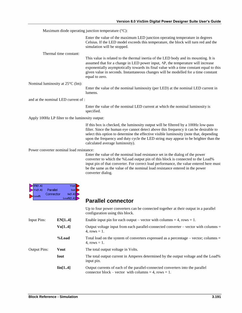
Version 8.0 VisSim Digital Power Designer Suite User’s Guide
Block Reference - Simulation 3.191
Maximum diode operating junction temperature (°C):
Enter the value of the maximum LED junction operating temperature in degrees
Celsius. If the LED model exceeds this temperature, the block will turn red and the
simulation will be stopped.
Thermal time constant:
This value is related to the thermal inertia of the LED body and its mounting. It is
assumed that for a change in LED power input, P, the temperature will increase
exponentially asymptotically towards its final value with a time constant equal to this
given value in seconds. Instantaneous changes will be modelled for a time constant
equal to zero.
Nominal luminosity at 25°C (lm):
Enter the value of the nominal luminosity (per LED) at the nominal LED current in
lumens.
and at the nominal LED current of :
Enter the value of the nominal LED current at which the nominal luminosity is
specified.
Apply 100Hz LP filter to the luminosity output:
If this box is checked, the luminosity output will be filtered by a 100Hz low-pass
filter. Since the human eye cannot detect above this frequency it can be desirable to
select this option to determine the effective visible luminosity (note that, depending
upon the frequency and duty cycle the LED string may appear to be brighter than the
calculated average luminosity).
Power converter nominal load resistance:
Enter the value of the nominal load resistance set in the dialog of the power
converter to which the %Load output pin of this block is connected to the Load%
input pin of that converter. For correct load performance, the value entered here must
be the same as the value of the nominal load resistance entered in the power
converter dialog.
Parallel connector
Up to four power converters can be connected together at their output in a parallel
configuration using this block.
Input Pins: EN[1..4] Enable input pin for each output – vector with columns = 4, rows = 1.
Vo[1..4] Output voltage input from each parallel-connected converter – vector with columns =
4, rows = 1.
%Load Total load on the system of converters expressed as a percentage – vector; columns =
4, rows = 1.
Output Pins: Vout The total output voltage in Volts.
Iout The total output current in Amperes determined by the output voltage and the Load%
input pin.
Iin[1..4] Output currents of each of the parallel-connected converters into the parallel
connector block – vector with columns = 4, rows = 1.
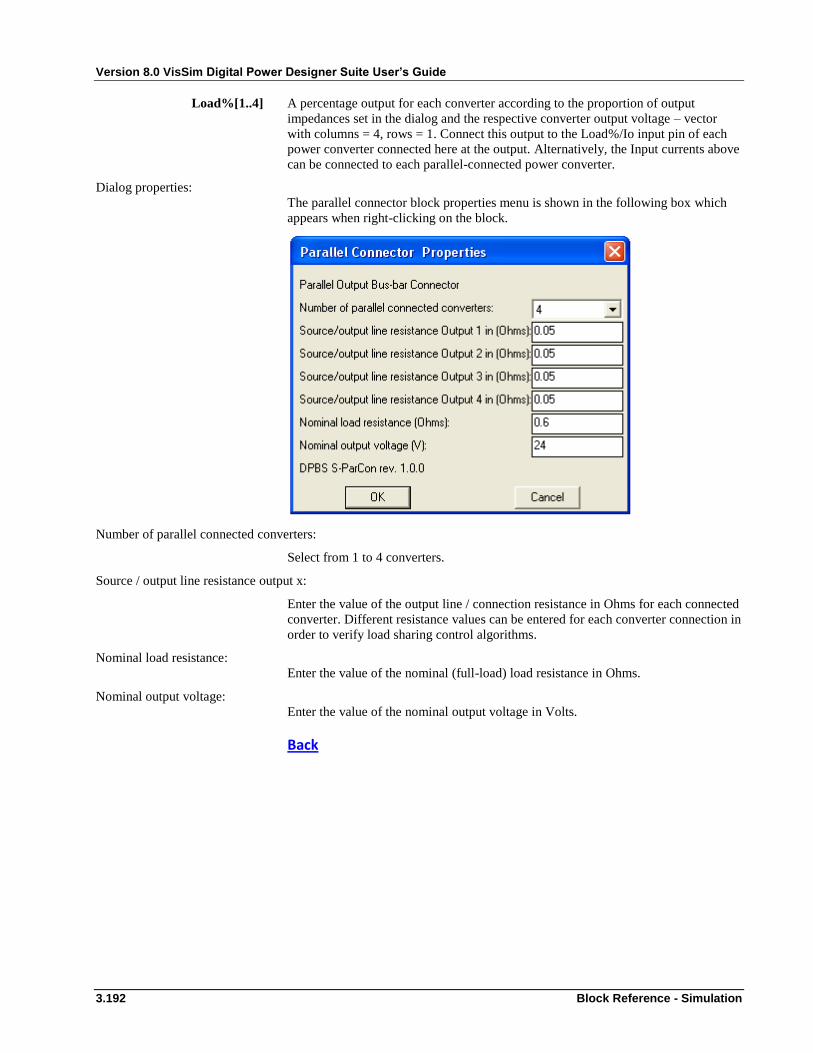
Version 8.0 VisSim Digital Power Designer Suite User’s Guide
3.192 Block Reference - Simulation
Load%[1..4] A percentage output for each converter according to the proportion of output
impedances set in the dialog and the respective converter output voltage – vector
with columns = 4, rows = 1. Connect this output to the Load%/Io input pin of each
power converter connected here at the output. Alternatively, the Input currents above
can be connected to each parallel-connected power converter.
Dialog properties:
The parallel connector block properties menu is shown in the following box which
appears when right-clicking on the block.
Number of parallel connected converters:
Select from 1 to 4 converters.
Source / output line resistance output x:
Enter the value of the output line / connection resistance in Ohms for each connected
converter. Different resistance values can be entered for each converter connection in
order to verify load sharing control algorithms.
Nominal load resistance:
Enter the value of the nominal (full-load) load resistance in Ohms.
Nominal output voltage:
Enter the value of the nominal output voltage in Volts.
Back
Chapter 4 – Contents
BLOCK REFERENCE - TOOLS ..................................................................................................................... 2
Block Convention .......................................................................................................................................................... 2
Compensators ............................................................................................................................................................... 3 PI Compensator ................................................................................................................................................................ 3 PID Compensator (2p2z) ................................................................................................................................................... 5 Type II Compensator ......................................................................................................................................................... 8 Type III Compensator ...................................................................................................................................................... 11
Filters .......................................................................................................................................................................... 14 Sallen-key 2
nd-order Low-pass Filter ............................................................................................................................... 14
Sallen-key 2nd
-order High-pass Filter .............................................................................................................................. 16 Sallen-key 2
nd-order Band-pass Filter ............................................................................................................................. 18
Coefficient Converters ................................................................................................................................................ 20

Version 8.0 VisSim Digital Power Designer Suite User’s Guide
Block Reference - Tools 4.2
Block Reference - Tools
The tools section of the digital power designer suite consists of a series of tools
which can be used by analog designers to directly convert familiar analog circuits
into digital filters and compensators.
The blocks in this section are therefore designed to be tools to assist in the
development of digital power control algorithms. The blocks can also be used
together with blocks from the simulation section to create simulation diagrams.
The tools in this section can also be used to convert between various formats of the
coefficients e.g. form analog to digital or from PID gains to poles and zeros etc.
Block Convention
The blocks within the tools environment are colour-coded in orange in order to
distinguish them from simulation and code-generable blocks. In general, bitmaps are
used with an orange background. The blocks can be customized if so desired by CTL
+ right clicking on the block to bring up the compound block properties dialog.
The blocks in this section are designed to be used as tools and are not code-
generable.

Version 8.0 VisSim Digital Power Designer Suite User’s Guide
4.3 Block Reference - Tools
Compensators
PI Compensator
Input pins: Vi(t) Input signal (optional)
Output pins: Vo(s) Vout (s-domain or continuous) which can be used in simulation.
Vo(z) Vout (z-domain or discrete) which can be used in simulation
Kx The gain coefficients output display (struct).
p&z Equivalent poles and zeros output display (struct).
H(s) Compensator coefficients in the s-domain (struct).
H(z) Compensator coefficients in the z-domain (struct).
Dialog properties:
The PI compensator block properties menu is shown in the following box which
appears when right-clicking on the block.
Version 8.0 VisSim Digital Power Designer Suite User’s Guide
Block Reference - Tools 4.4
Compensator sampling frequency:
Enter the value of the sampling frequency (for a digital filter using z-coefficients).
R1:
Enter the value of the block circuit schematic resistance R1 in kilo-Ohms.
R2:
Enter the value of the block circuit schematic resistance R2 in kilo-Ohms
C1:
Enter the value of the block circuit schematic resistance C1 in nano-Farads
Enter converter parameters (PCMC-CCM):
Select this check box if you choose to calculate the required coefficients using
parameters based upon the converter power stage design. The parameters will be
valid for Peak current mode control (PCMC) in continuous conduction mode (CCM).
Converter Topology:
The choices here are:
1. Buck
2. Boost
3. Buck-boost
For other topologies, one of the above choices can be used. For example, for a half-
bridge, full-bridge, push-pull or forward topology, the buck topology can be selected.
For a flyback topology, the buck-boost topology can be selected here.
Current Measurement gain:
Enter the gain of the current measurement network (sensor) in V/A.
Converter Inductance:
Insert the value of the converter inductance in microHenries.
Switching Frequency, Fsw:
Insert the converter switching frequency in kHz.
Nominal Input Voltage:
Enter the nominal input voltage of the converter in Volts.
Nominal Output Voltage:
Enter the nominal output voltage of the converter in Volts.
Compensating Ramp Slope:
Enter the desired value of the slope compensation ramp in V / switching period.
Load Resistance:
Insert the value of the nominal load resistance in Ohms.
Output Capacitance:
Insert the value of the output capacitance in microfarads.
Output Capacitor ESR:
Insert the value of the output capacitor equivalent series resistance (ESR) in Ohms.
Desired gain cross-over frequency:
Enter the value of the desired gain cross-over frequency (bandwidth of the control
loop) in kHz.
Enter directly the desired gain coefficients:
Check this box if the previous input parameters are to be ignored and enter directly
the gain parameters as below.
Proportional gain, Kp:
Enter the value of the proportional gain.
Integral gain, Ki:
Enter the value of the integral gain.
Enter directly the desired poles and zeros:
Check this box if the previous input parameters and gain coefficients are to be
ignored and enter directly the poles and zeros as below.
Pole at the origin, Fp0:
Enter the value of the pole of the first-order transfer function (at the origin).

Version 8.0 VisSim Digital Power Designer Suite User’s Guide
4.5 Block Reference - Tools
First zero, Fz1:
Enter the value of the zero of the transfer function.
Export gain coefficients to file:
Check this box if it is desired to export the gain coefficients to a chosen file.
File path and name:
Enter the file name and path to the location of the file.
Export z-coefficients to file:
Check this box if it is desired to export the z-coefficients to a chosen file.
File path and name:
Enter the file name and path to the location of the file.
Back
PID Compensator (2p2z)
Input pins: Vi(t) Input signal (optional)
Output pins: Vo(s) Vout (s-domain or continuous) which can be used in simulation.
Vo(z) Vout (z-domain or discrete) which can be used in simulation
Kx The gain coefficients output display (struct).
p&z Equivalent poles and zeros output display (struct).
H(s) Compensator coefficients in the s-domain (struct).
H(z) Compensator coefficients in the z-domain (struct).
Dialog properties:
The PID compensator block properties menu is shown in the following box which
appears when right-clicking on the block.

Version 8.0 VisSim Digital Power Designer Suite User’s Guide
Block Reference - Tools 4.6
Compensator sampling frequency:
Enter the value of the sampling frequency (for a digital filter using z-coefficients).
R1:
Enter the value of the block circuit schematic resistance R1 in kilo-Ohms.
R2:
Enter the value of the block circuit schematic resistance R2 in kilo-Ohms.
R3:
Enter the value of the block circuit schematic resistance R3 in kilo-Ohms.
C1:
Enter the value of the block circuit schematic resistance C1 in nano-Farads.
C2:
Enter the value of the block circuit schematic resistance C2 in nano-Farads.
Enter converter parameters (VMC):
Select this check box if you choose to calculate the required coefficients using
parameters based upon the converter power stage design. The parameters will be
valid for voltage mode control (VMC) in continuous conduction mode (CCM).
Converter Topology:
The choices here are:
1. Buck
2. Boost
3. Buck-boost
Version 8.0 VisSim Digital Power Designer Suite User’s Guide
4.7 Block Reference - Tools
For other topologies, one of the above choices can be used. For example, for a half-
bridge, full-bridge, push-pull or forward topology, the buck topology can be selected.
For a flyback topology, the buck-boost topology can be selected here.
ADC gain:
Enter the gain of the current measurement network (sensor) in V/A.
DPWM gain:
Enter the effective gain of the digital PWM modulator in V/V.
Converter Inductance:
Insert the value of the converter inductance in microHenries.
Switching Frequency, Fsw:
Insert the converter switching frequency in kHz.
Nominal Input Voltage:
Enter the nominal input voltage of the converter in Volts.
Nominal Output Voltage:
Enter the nominal output voltage of the converter in Volts.
Output Capacitance:
Insert the value of the output capacitance in microfarads.
Output Capacitor ESR:
Insert the value of the output capacitor equivalent series resistance (ESR) in Ohms.
Desired gain cross-over frequency:
Enter the value of the desired gain cross-over frequency (bandwidth of the control
loop) in kHz.
Enter directly the desired gain coefficients:
Check this box if the previous input parameters are to be ignored and enter directly
the gain parameters as below.
Proportional gain, Kp:
Enter the value of the proportional gain.
Integral gain, Ki:
Enter the value of the integral gain.
Differential gain, Kd:
Enter the value of the differential gain.
Differential part LP filter gain, N:
Enter the value of the low-pass filter gain divider of the differential gain.
Enter directly the desired poles and zeros:
Check this box if the previous input parameters are to be ignored and enter directly
the poles and zeros of the compensator as below.
Pole at the origin, Fp0:
Enter the value of the pole at the origin of the second-order transfer function.
First pole, Fp1:
Enter the value of the pole of the second order transfer function.
First zero, Fz1:
Enter the value of the first zero of the second-order transfer function.
Second zero, Fz2:
Enter the value of the second zero of the second order transfer function.
Export gain coefficients to file:
Check this box if it is desired to export the gain coefficients to a chosen file.
File path and name:
Enter the file name and path to the location of the file.

Version 8.0 VisSim Digital Power Designer Suite User’s Guide
Block Reference - Tools 4.8
Export z-coefficients to file:
Check this box if it is desired to export the z-coefficients to a chosen file.
File path and name:
Enter the file name and path to the location of the file.
Back
Type II Compensator
Input pins: Vi(t) Input signal (optional)
Output pins: Vo(s) Vout (s-domain or continuous) which can be used in simulation.
Vo(z) Vout (z-domain or discrete) which can be used in simulation
Kx The gain coefficients output display (struct).
p&z Equivalent poles and zeros output display (struct).
H(s) Compensator coefficients in the s-domain (struct).
H(z) Compensator coefficients in the z-domain (struct).
Dialog properties:
The Type II compensator block properties menu is shown in the following box
which appears when right-clicking on the block.

Version 8.0 VisSim Digital Power Designer Suite User’s Guide
4.9 Block Reference - Tools
Compensator sampling frequency:
Enter the value of the sampling frequency (for a digital filter using z-coefficients).
R1:
Enter the value of the block circuit schematic resistance R1 in kilo-Ohms.
R2:
Enter the value of the block circuit schematic resistance R2 in kilo-Ohms
C1:
Enter the value of the block circuit schematic resistance C1 in nano-Farads
C2:
Enter the value of the block circuit schematic resistance C2 in nano-Farads
Enter converter parameters (PCMC-CCM):
Select this check box if you choose to calculate the required coefficients using
parameters based upon the converter power stage design. The parameters will be
valid for Peak current mode control (PCMC) in continuous conduction mode (CCM).
Converter Topology:
The choices here are:
1. Buck
2. Boost
3. Buck-boost
For other topologies, one of the above choices can be used. For example, for a half-
bridge, full-bridge, push-pull or forward topology, the buck topology can be selected.
For a flyback topology, the buck-boost topology can be selected here.
Current Measurement gain:
Enter the gain of the current measurement network (sensor) in V/A.
Version 8.0 VisSim Digital Power Designer Suite User’s Guide
Block Reference - Tools 4.10
Converter Inductance:
Insert the value of the converter inductance in microHenries.
Switching Frequency, Fsw:
Insert the converter switching frequency in kHz.
Nominal Input Voltage:
Enter the nominal input voltage of the converter in Volts.
Nominal Output Voltage:
Enter the nominal output voltage of the converter in Volts.
Compensating Ramp Slope:
Enter the desired value of the slope compensation ramp in V / switching period.
Load Resistance:
Insert the value of the nominal load resistance in Ohms.
Output Capacitance:
Insert the value of the output capacitance in microfarads.
Output Capacitor ESR:
Insert the value of the output capacitor equivalent series resistance (ESR) in Ohms.
Desired gain cross-over frequency:
Enter the value of the desired gain cross-over frequency (bandwidth of the control
loop) in kHz.
Enter directly the desired poles and zeros:
Check this box if the previous input parameters are to be ignored and enter directly
the poles and zeros as below.
Pole at the origin, Fp0:
Enter the value of the pole at the origin in kHz.
First pole, Fp1:
Enter the value of the first pole of the compensator in kHz.
First zero, Fz1:
Enter the value of the first zero of the compensator in kHz.
Export poles and zeros to file:
Check this box if it is desired to export the poles and zeros to a chosen file.
File path and name:
Enter the file name and path to the location of the file.
Export z-coefficients to file:
Check this box if it is desired to export the z-coefficients to a chosen file.
File path and name:
Enter the file name and path to the location of the file.
Back
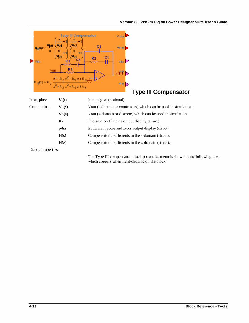
Version 8.0 VisSim Digital Power Designer Suite User’s Guide
4.11 Block Reference - Tools
Type III Compensator
Input pins: Vi(t) Input signal (optional)
Output pins: Vo(s) Vout (s-domain or continuous) which can be used in simulation.
Vo(z) Vout (z-domain or discrete) which can be used in simulation
Kx The gain coefficients output display (struct).
p&z Equivalent poles and zeros output display (struct).
H(s) Compensator coefficients in the s-domain (struct).
H(z) Compensator coefficients in the z-domain (struct).
Dialog properties:
The Type III compensator block properties menu is shown in the following box
which appears when right-clicking on the block.

Version 8.0 VisSim Digital Power Designer Suite User’s Guide
Block Reference - Tools 4.12
Compensator sampling frequency:
Enter the value of the sampling frequency (for a digital filter using z-coefficients).
R1:
Enter the value of the block circuit schematic resistance R1 in kilo-Ohms.
R2:
Enter the value of the block circuit schematic resistance R2 in kilo-Ohms
R3:
Enter the value of the block circuit schematic resistance R3 in kilo-Ohms
C1:
Enter the value of the block circuit schematic resistance C1 in nano-Farads
C2:
Enter the value of the block circuit schematic resistance C2 in nano-Farads.
C3:
Enter the value of the block circuit schematic resistance C3 in nano-Farads.
Enter converter parameters (VMC):
Select this check box if you choose to calculate the required coefficients using
parameters based upon the converter power stage design. The parameters will be
valid for voltage mode control (VMC) in continuous conduction mode (CCM).
Converter Topology:
The choices here are:
1. Buck
2. Boost
3. Buck-boost
Version 8.0 VisSim Digital Power Designer Suite User’s Guide
4.13 Block Reference - Tools
For other topologies, one of the above choices can be used. For example, for a half-
bridge, full-bridge, push-pull or forward topology, the buck topology can be selected.
For a flyback topology, the buck-boost topology can be selected here.
ADC gain:
Enter the gain of the current measurement network (sensor) in V/A.
DPWM gain:
Enter the effective gain of the digital PWM modulator in V/V.
Converter Inductance:
Insert the value of the converter inductance in microHenries.
Switching Frequency, Fsw:
Insert the converter switching frequency in kHz.
Nominal Input Voltage:
Enter the nominal input voltage of the converter in Volts.
Nominal Output Voltage:
Enter the nominal output voltage of the converter in Volts.
Output Capacitance:
Insert the value of the output capacitance in microfarads.
Output Capacitor ESR:
Insert the value of the output capacitor equivalent series resistance (ESR) in Ohms.
Desired gain cross-over frequency:
Enter the value of the desired gain cross-over frequency (bandwidth of the control
loop) in kHz.
Enter directly the desired poles and zeros:
Check this box if the previous input parameters are to be ignored and enter directly
the poles and zeros as below.
Pole at the origin, Fp0:
Enter the value of the pole at the origin in kHz.
First pole, Fp1:
Enter the value of the first pole of the compensator in kHz.
First zero, Fz1:
Enter the value of the first zero of the compensator in kHz.
First pole, Fp2:
Enter the value of the second pole of the compensator in kHz.
First zero, Fz2:
Enter the value of the second zero of the compensator in kHz.
Export poles and zeros to file:
Check this box if it is desired to export the poles and zeros to a chosen file.
File path and name:
Enter the file name and path to the location of the file.
Export z-coefficients to file:
Check this box if it is desired to export the z-coefficients to a chosen file.
File path and name:
Enter the file name and path to the location of the file.
Back
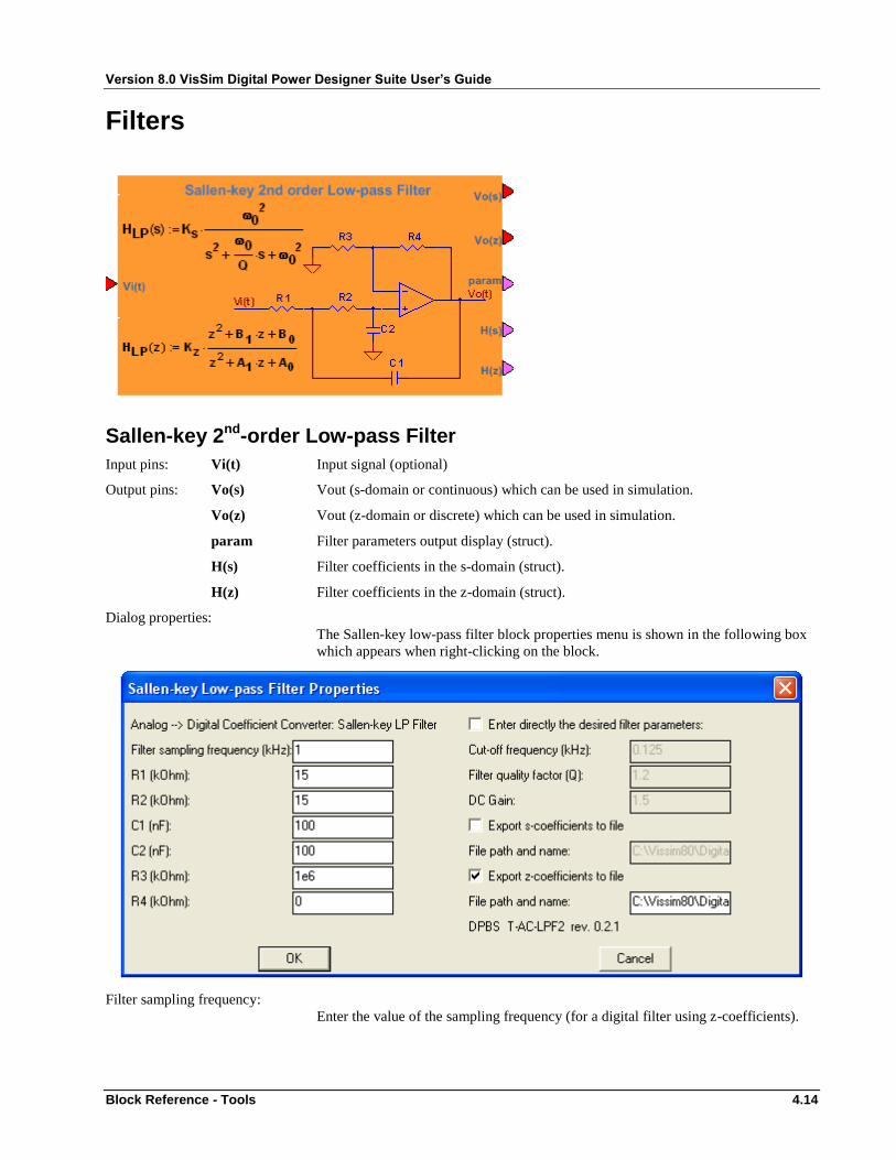
Version 8.0 VisSim Digital Power Designer Suite User’s Guide
Block Reference - Tools 4.14
Filters
Sallen-key 2nd-order Low-pass Filter
Input pins: Vi(t) Input signal (optional)
Output pins: Vo(s) Vout (s-domain or continuous) which can be used in simulation.
Vo(z) Vout (z-domain or discrete) which can be used in simulation.
param Filter parameters output display (struct).
H(s) Filter coefficients in the s-domain (struct).
H(z) Filter coefficients in the z-domain (struct).
Dialog properties:
The Sallen-key low-pass filter block properties menu is shown in the following box
which appears when right-clicking on the block.
Filter sampling frequency:
Enter the value of the sampling frequency (for a digital filter using z-coefficients).

Version 8.0 VisSim Digital Power Designer Suite User’s Guide
4.15 Block Reference - Tools
R1:
Enter the value of the block circuit schematic resistance R1 in kilo-Ohms.
R2:
Enter the value of the block circuit schematic resistance R2 in kilo-Ohms
C1:
Enter the value of the block circuit schematic resistance C1 in nano-Farads
C2:
Enter the value of the block circuit schematic resistance C2 in nano-Farads
R3:
Enter the value of the block circuit schematic resistance R3 in kilo-Ohms.
R4:
Enter the value of the block circuit schematic resistance R4 in kilo-Ohms
Enter directly the desired filter parameters:
Check this box if the previous circuit values are to be ignored and enter directly the
filter parameters as below.
Center Frequency, Fo:
Enter the value of the required cut-off frequency in kHz of the low-pass filter.
Filter quality factor, Q:
Enter the value of the required filter quality factor, Q.
DC gain, Ks:
Enter the required value of the low-frequency gain of the low-pass filter.
Export s-coefficients to file:
Check this box if it is desired to export the gain coefficients to a chosen file.
File path and name:
Enter the file name and path to the location of the file.
Export z-coefficients to file:
Check this box if it is desired to export the z-coefficients to a chosen file.
File path and name:
Enter the file name and path to the location of the file.
Back

Version 8.0 VisSim Digital Power Designer Suite User’s Guide
Block Reference - Tools 4.16
Sallen-key 2nd-order High-pass Filter
Input pins: Vi(t) Input signal (optional)
Output pins: Vo(s) Vout (s-domain or continuous) which can be used in simulation.
Vo(z) Vout (z-domain or discrete) which can be used in simulation.
param Filter parameters output display (struct).
H(s) Filter coefficients in the s-domain (struct).
H(z) Filter coefficients in the z-domain (struct).
Dialog properties:
The Sallen-key high-pass filter block properties menu is shown in the following box
which appears when right-clicking on the block.
Filter sampling frequency:
Enter the value of the sampling frequency (for a digital filter using z-coefficients).
R1:
Enter the value of the block circuit schematic resistance R1 in kilo-Ohms.
Version 8.0 VisSim Digital Power Designer Suite User’s Guide
4.17 Block Reference - Tools
R2:
Enter the value of the block circuit schematic resistance R2 in kilo-Ohms
C1:
Enter the value of the block circuit schematic resistance C1 in nano-Farads
C2:
Enter the value of the block circuit schematic resistance C2 in nano-Farads
R3:
Enter the value of the block circuit schematic resistance R3 in kilo-Ohms.
R4:
Enter the value of the block circuit schematic resistance R4 in kilo-Ohms
Enter directly the desired filter parameters:
Check this box if the previous circuit values are to be ignored and enter directly the
filter parameters as below.
Center Frequency, Fo:
Enter the value of the required cut-off frequency in kHz of the high-pass filter.
Filter quality factor, Q:
Enter the value of the required filter quality factor, Q.
High frequency gain, Ks:
Enter the required value of the high-frequency gain of the high-pass filter.
Export s-coefficients to file:
Check this box if it is desired to export the gain coefficients to a chosen file.
File path and name:
Enter the file name and path to the location of the file.
Export z-coefficients to file:
Check this box if it is desired to export the z-coefficients to a chosen file.
File path and name:
Enter the file name and path to the location of the file.
Back
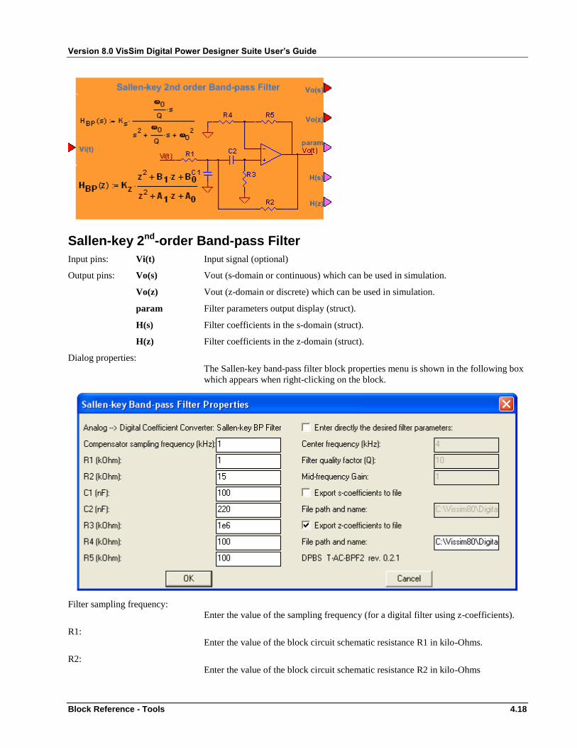
Version 8.0 VisSim Digital Power Designer Suite User’s Guide
Block Reference - Tools 4.18
Sallen-key 2nd-order Band-pass Filter
Input pins: Vi(t) Input signal (optional)
Output pins: Vo(s) Vout (s-domain or continuous) which can be used in simulation.
Vo(z) Vout (z-domain or discrete) which can be used in simulation.
param Filter parameters output display (struct).
H(s) Filter coefficients in the s-domain (struct).
H(z) Filter coefficients in the z-domain (struct).
Dialog properties:
The Sallen-key band-pass filter block properties menu is shown in the following box
which appears when right-clicking on the block.
Filter sampling frequency:
Enter the value of the sampling frequency (for a digital filter using z-coefficients).
R1:
Enter the value of the block circuit schematic resistance R1 in kilo-Ohms.
R2:
Enter the value of the block circuit schematic resistance R2 in kilo-Ohms
Version 8.0 VisSim Digital Power Designer Suite User’s Guide
4.19 Block Reference - Tools
C1:
Enter the value of the block circuit schematic resistance C1 in nano-Farads
C2:
Enter the value of the block circuit schematic resistance C2 in nano-Farads
R3:
Enter the value of the block circuit schematic resistance R3 in kilo-Ohms.
R4:
Enter the value of the block circuit schematic resistance R4 in kilo-Ohms
R5:
Enter the value of the block circuit schematic resistance R5 in kilo-Ohms.
Enter directly the desired filter parameters:
Check this box if the previous circuit values are to be ignored and enter directly the
filter parameters as below.
Center Frequency:
Enter the value of the required center frequency in kHz of the band-pass filter.
Filter quality factor:
Enter the value of the required filter quality factor, Q.
Mid-frequency gain:
Enter the required value of the mid-frequency gain of the band-pass filter.
Export s-coefficients to file:
Check this box if it is desired to export the gain coefficients to a chosen file.
File path and name:
Enter the file name and path to the location of the file.
Export z-coefficients to file:
Check this box if it is desired to export the z-coefficients to a chosen file.
File path and name:
Enter the file name and path to the location of the file.
Back

Version 8.0 VisSim Digital Power Designer Suite User’s Guide
Block Reference - Tools 4.20
Coefficient Converters
The direct coefficient converter tools are intended to be used in diagrams where
interactive simulations can be performed to observe the converter control behaviour
when changing the compensator coefficients during the simulation. The blocks
directly translate from the familiar poles and zeros or PID gain coefficients to the
more unfamiliar discrete z-coefficients. They would normally be used in conjunction
with the compensators with pins from the components section. The output z-
coefficients are of a form consistent with the digital power design suite as:
Input pins: Wpx Input pole (radians) which would normally be connected from a slider.
Wzx Input zero (radians) which would normally be connected from a slider.
Kx PID gain which would normally be connected from a slider.
Output pins: Kz Discrete z-coefficients gain
Bx Numerator discrete z-coefficients
Ax Denominator discrete z-coefficients
Dialog properties:
The coefficient converter blocks properties menu is shown in the following box
which appears when right-clicking on any of the coefficient converter blocks.
Sampling frequency (kHz):
Enter the value of the desired sampling frequency. Note that changing the sampling
frequency will result in changing the z-coefficients and this value is very important
for correct coefficient conversion.
H3 z( ) Kz
z3
B2 z2
B1 z B0
z3
A2 z2
A1 z A0
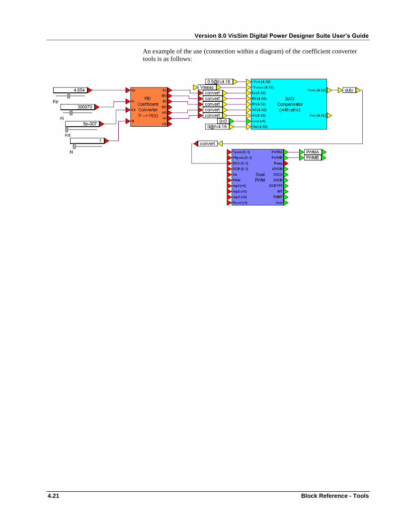
Version 8.0 VisSim Digital Power Designer Suite User’s Guide
4.21 Block Reference - Tools
An example of the use (connection within a diagram) of the coefficient converter
tools is as follows:
![VISSIM Lab Assignment_Final[1]](https://static.fdocuments.us/doc/165x107/55cf9aa0550346d033a2a24a/vissim-lab-assignmentfinal1.jpg)