Virtual resistance based DC-link voltage regulation for ...
119
University of Central Florida University of Central Florida STARS STARS Electronic Theses and Dissertations 2016 Virtual resistance based DC-link voltage regulation for Microgrid Virtual resistance based DC-link voltage regulation for Microgrid DG inverters. DG inverters. Siddhesh Shinde University of Central Florida Part of the Electrical and Computer Engineering Commons Find similar works at: https://stars.library.ucf.edu/etd University of Central Florida Libraries http://library.ucf.edu This Masters Thesis (Open Access) is brought to you for free and open access by STARS. It has been accepted for inclusion in Electronic Theses and Dissertations by an authorized administrator of STARS. For more information, please contact [email protected]. STARS Citation STARS Citation Shinde, Siddhesh, "Virtual resistance based DC-link voltage regulation for Microgrid DG inverters." (2016). Electronic Theses and Dissertations. 5251. https://stars.library.ucf.edu/etd/5251
Transcript of Virtual resistance based DC-link voltage regulation for ...
University of Central Florida University of Central Florida
STARS STARS
Electronic Theses and Dissertations
2016
Virtual resistance based DC-link voltage regulation for Microgrid Virtual resistance based DC-link voltage regulation for Microgrid
DG inverters. DG inverters.
Siddhesh Shinde University of Central Florida
Part of the Electrical and Computer Engineering Commons
Find similar works at: https://stars.library.ucf.edu/etd
University of Central Florida Libraries http://library.ucf.edu
This Masters Thesis (Open Access) is brought to you for free and open access by STARS. It has been accepted for
inclusion in Electronic Theses and Dissertations by an authorized administrator of STARS. For more information,
please contact [email protected].
STARS Citation STARS Citation Shinde, Siddhesh, "Virtual resistance based DC-link voltage regulation for Microgrid DG inverters." (2016). Electronic Theses and Dissertations. 5251. https://stars.library.ucf.edu/etd/5251
VIRTUAL RESISTANCE BASED DC-LINK VOLTAGE REGULATION FOR MICROGRID DG INVERTERS
by
SIDDHESH SHINDE B.E. University of Mumbai, 2012
A thesis submitted in partial fulfillment of the requirements for the degree of Master of Science
in the Department of Electrical and Computer Engineering in the College of Engineering and Computer Science
at the University of Central Florida Orlando, Florida
Fall Term 2016
Major Professor: Issa Batarseh

ii
© 2016 Siddhesh Shinde
iii
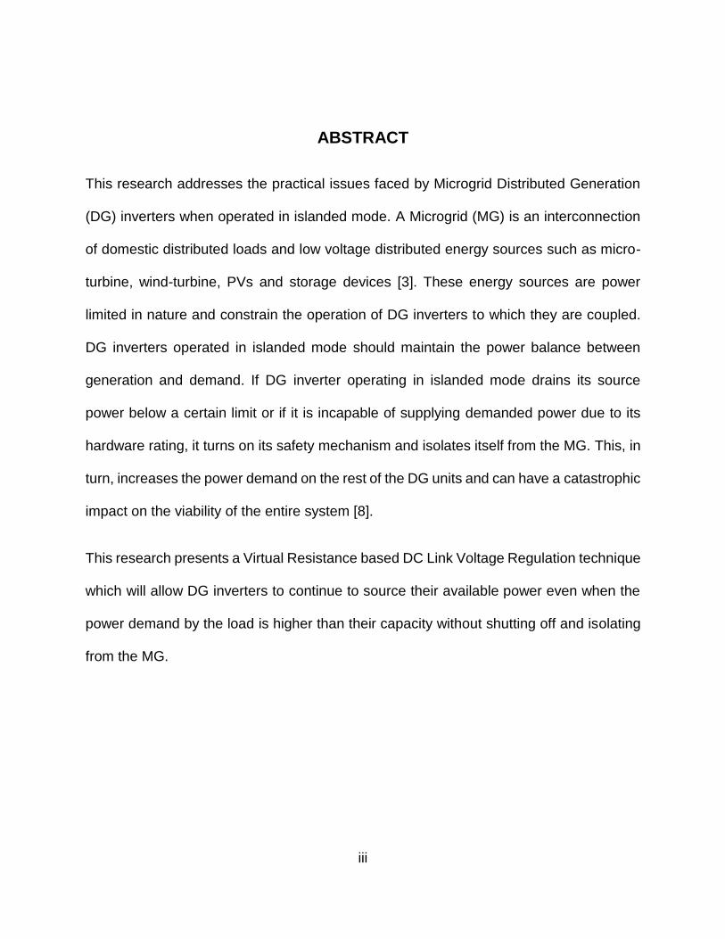
ABSTRACT
This research addresses the practical issues faced by Microgrid Distributed Generation
(DG) inverters when operated in islanded mode. A Microgrid (MG) is an interconnection
of domestic distributed loads and low voltage distributed energy sources such as micro-
turbine, wind-turbine, PVs and storage devices [3]. These energy sources are power
limited in nature and constrain the operation of DG inverters to which they are coupled.
DG inverters operated in islanded mode should maintain the power balance between
generation and demand. If DG inverter operating in islanded mode drains its source
power below a certain limit or if it is incapable of supplying demanded power due to its
hardware rating, it turns on its safety mechanism and isolates itself from the MG. This, in
turn, increases the power demand on the rest of the DG units and can have a catastrophic
impact on the viability of the entire system [8].
This research presents a Virtual Resistance based DC Link Voltage Regulation technique
which will allow DG inverters to continue to source their available power even when the
power demand by the load is higher than their capacity without shutting off and isolating
from the MG.

iv
Dedicated to my parents who inspired me

v
ACKNOWLEDGMENTS
I always thought a miracle is meeting the right person at the right time in life; I want to
thank Dr. Issa Batarseh for giving me an opportunity to work with him at Florida Power
Electronics Center and contribute to his research. I would like to thank Mr. Charlie
Jourdan and Dr. Hussam Alatrash for providing intellectual insights throughout my
research; I consider them as my ideal who not only inspired me but also helped me build
a strong foundation for learning and facing real-life challenges.
I am grateful to the research group at FPEC - Milad Tayebi, Anirudh Pise, Mahmood
Alharbi, Xi Chen, Michael Pepper and Christopher Hamilton for their support and
intellectual discussions. I am thankful to my committee members Dr. Issa Batarseh, Dr.
Nasser Kutkut and Dr. Mikhael Wasfy who gave me their guidance and expert judgment
during the completion of the thesis. I am thankful to Ms. Carol Ann Dykes for her kindness
in helping me editing this document.
Finally, I am grateful to my family, friends for their kind understanding and constant
support.

vi
TABLE OF CONTENTS
LIST OF FIGURES .......................................................................................................... x
LIST OF TABLES ...........................................................................................................xv
CHAPTER 1: INTRODUCTION ....................................................................................... 1
1.1 Microgrid ............................................................................................................ 1
1.1.1 Microgrid Structure and Control ................................................................... 2
1.2 Microsources ...................................................................................................... 5
1.2.1 Inverters with Photovoltaic Microsource ...................................................... 8
1.2.2 Inverters with Battery Microsource .............................................................. 9
1.3 DG Unit Control Strategies ................................................................................. 9
1.3.1 Droop based Control Strategy ................................................................... 11
1.3.2 Virtual Synchronous Machine Based Control Strategy .............................. 15
1.4 Power Limit Management for Grid-Forming Inverters. ..................................... 18
1.5 Outline of the Thesis ........................................................................................ 19
CHAPTER 2: CONTROLS OF THE GRID-FOLLOWING INVERTERS ........................ 21
vii
2.1 Basic Blocks of the Inverter .............................................................................. 21
2.2 PLL for Grid-following Inverters ........................................................................ 23
2.2.1 PLL Structure ............................................................................................. 24
2.2.2 PLL Modeling and Control Design ............................................................. 26
2.2.3 PLL Implementation ................................................................................... 30
2.3 OCR for Grid-following Inverter ........................................................................ 35
2.3.1 OCR Dynamics .......................................................................................... 36
2.3.2 OCR Plant Modeling and Controller Design .............................................. 38
2.3.3 OCR Hardware Results ............................................................................. 42
2.3.4 OCR Implementation ................................................................................. 43
CHAPTER 3: GENERATOR EMULATION CONTROL FOR THE INVERTERS ........... 47
3.1 Dynamic Properties of Synchronous Generator ............................................... 48
3.1.1 P-𝜔 Droop Control ..................................................................................... 52
3.1.2 Damping and Inertial Properties of Synchronous Generator ..................... 54
3.2 Generator Emulation Controls .......................................................................... 55
viii
3.2.1 Impedance emulation ................................................................................ 56
3.2.2 Droop-based PLL ...................................................................................... 58
3.3 GEC Implementation and Design Consideration .............................................. 62
3.3.1 Design of stator inductor 𝑳𝒔 and DC resistance 𝑅𝑑𝑐 ................................. 63
3.3.2 Design of Proportional Gain for Droop-Based PLL .................................... 65
3.3.3 Simulink Implementation of GEC ............................................................... 69
3.4 GEC Inverter Hardware Results ....................................................................... 71
CHAPTER 4: VIRTUAL RESISTANCE BASED DC-LINK VOLTAGE REGULATION FOR
GEC INVERTERS ......................................................................................................... 76
4.1 DC-link voltage regulator for Grid-following Inverter ......................................... 76
4.2 DC-link voltage regulator for GEC grid-forming Inverter using virtual resistance
technique ................................................................................................................... 79
4.3 Modeling and Control Design for DC-link voltage regulator ............................. 83
4.4 Implementation of Virtual Resistance based DC-link Voltage Regulator .......... 90
4.5 Results of Virtual Resistance based DC-link Regulator ................................... 94
CHAPTER 5: CONCLUSION ........................................................................................ 96
ix
APPENDIX: EXPERIMENTAL SETUP .......................................................................... 98
LIST OF REFERENCES ............................................................................................. 101

x
LIST OF FIGURES
Figure 1-1: Simplified structure and controls of the Microgrid ......................................... 3
Figure 1-2: Stages of inverter based DG ......................................................................... 6
Figure 1-3: Categorization of the inverter based DG controls ....................................... 10
Figure1-4: Q-E and P-𝜔 Droop control .......................................................................... 13
Figure 1-5: Implementation of PQ droop control strategy .............................................. 14
Figure 1-6: Implementation of VSG control strategy ..................................................... 17
Figure 2-1: Basic Blocks of grid-following inverter ......................................................... 21
Figure 2-2: Basic structure of PLL ................................................................................. 24
Figure 2-3: S-domain representation of PLL ................................................................. 27
Figure 2-4: PLL uncompensated loop gain .................................................................... 29
Figure 2-5: PLL compensated loop gain ........................................................................ 30
Figure 2-6: PLL Simulink Implementation ...................................................................... 30
Figure 2-7: Low pass filter implementation .................................................................... 32
Figure 2-8: Digital PI-controller implementation ............................................................ 33

xi
Figure 2-9: Implementation of NCO............................................................................... 35
Figure 2-10: Output current regulator loop model ......................................................... 36
Figure 2-11: Inverter stage model for developing 𝐺𝑖𝑑(𝑠) ............................................... 38
Figure 2-12: Output current regulator with PI and feedforward control .......................... 39
Figure 2-13: OCR uncompensated loop gain ................................................................ 41
Figure 2-14: OCR compensated loop gain .................................................................... 42
Figure 2-15: Hardware results for OCR ......................................................................... 43
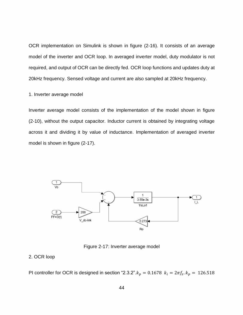
Figure 2-16: OCR loop and inverter average model ...................................................... 43
Figure 2-17: Inverter average model ............................................................................. 44
Figure 2-18: OCR implementation ................................................................................. 46
Figure 3-1: Basic block of power generator system ...................................................... 48
Figure 3-2: Electrical characteristics of synchronous generator .................................... 49
Figure 3-3: Dynamic model of synchronous generator .................................................. 51
Figure 3-4: Dynamic model of synchronous generator with droop control ..................... 52
Figure 3-5: P-ω droop negative slope relationship ........................................................ 53

xii
Figure 3-6: GEC impedance emulation ......................................................................... 57
Figure 3-7: S-domain model of PLL............................................................................... 58
Figure 3-8 Dynamic model of PLL ................................................................................. 60
Figure 3-9: Modified characteristics of emulated impedance network ........................... 63
Figure 3-10: P-ω droop curve for PV and battery DG inverters ..................................... 67
Figure 3-11: P-ω droop curve ........................................................................................ 67
Figure 3-12: Peak output current vs Phase error .......................................................... 68
Figure 3-13: GEC Implementation in Simulink .............................................................. 70
Figure 3-14: Implementation of GEC block ................................................................... 71
Figure 3-15: Output current at 59.30 Hz ........................................................................ 72
Figure 3-16: Output current at 59.40 Hz ........................................................................ 72
Figure 3-17: Output current at 59.50 Hz ........................................................................ 73
Figure 3-18: Output current at 59.60 Hz ........................................................................ 73
Figure 3-19: Output current at 59.70 Hz ........................................................................ 74
Figure 3-20: Output current at 59.80 Hz ........................................................................ 74

xiii
Figure 3-21: Output current at 59.90 Hz ........................................................................ 75
Figure 4-1: Single stage grid-following inverter ............................................................. 77
Figure 4-2: Grid-forming Inverters operated in islanded mode. ..................................... 80
Figure 4-3: GEC based grid-forming inverter ................................................................ 81
Figure 4-4: Virtual resistance integrated emulated impedance network ........................ 82
Figure 4-5: Dynamic model of DC-link voltage .............................................................. 85
Figure 4-6: Virtual resistance model .............................................................................. 86
Figure 4-7: Dynamic model of virtual resistance based DC-link voltage regulator ........ 87
Figure 4-8: Uncompensated DC-link voltage regulator loop gain .................................. 88
Figure 4-9: Compensated DC-link voltage regulator loop-gain ...................................... 90
Figure 4-10: Dynamic model of DC-link voltage and DC-link voltage regulator ............. 91
Figure 4-11: Virtual resistance embedded in GEC model ............................................. 93
Figure 4-12: GEC inverter with virtual resistance based DC-link voltage regulator ....... 94
Figure 4-13: DC-link voltage regulator........................................................................... 95
Figure 5-1: Power-limited P-𝜔 droop curve of GEC inverter ......................................... 97

xiv
Figure A-1: GEC inverter setup layout........................................................................... 99
Figure A-2: GEC inverter experimental setup .............................................................. 100
xv
LIST OF TABLES
Table 1-1: Droop characteristics based controls ........................................................... 15
Table 2-1: Values of PLL gain ....................................................................................... 28
Table 2-2: System parameters for designing OCR ........................................................ 40
Table 3-1: Inverter parameters to design stator inductor 𝐿𝑠 .......................................... 64
Table 3-2: Parameters to calculate droop PLL gain ...................................................... 68
Table 4-1: Inverter parameters to designing DC-link voltage regulator loop .................. 87
1
CHAPTER 1: INTRODUCTION
The increase in diverse power demand and environmental concerns has challenged the
reliability of the conventional power system which is based on a centralized architecture.
Distributed Generation (DG) offers an opportunity to achieve higher power system
reliability and efficiency due to its distributed nature. The increase in the penetration of
DG brings about a concept of the microgrid [2]. A microgrid is an interconnection of
domestic distributed loads and low voltage distributed energy sources such as micro-
turbine, wind-turbine, PVs and storage devices [3]. These energy sources are power
limited in nature and place constraints on the operation of DG units to which they are
coupled. In this research, the emphasis is placed on power-limit management techniques
which allow DG units to remain connected to the microgrid even when sourcing low
power. This avoids overloading of the rest of the resources connected in the microgrid
thus improving microgrid stability.
1.1 Microgrid
With the increase in DG and distributed storage (DS) on the low voltage (LV) side of the
grid, it is not technically or economically feasible to extend the traditional command and
control philosophy of the grid to these devices [1]. Microgrid technology is used to
overcome this problem. Microgrid forms the coordinated group of energy sources,
storages, and loads that can collectively interact with the main grid as a unified, coherent
system [1]. Microgrids provide a higher degree of freedom from controllability and
2
operability perspective as the burden of control and communication shifts away from the
centralized grid controller. They allow integration of distributed generation and distributed
storages on the LV side of the grid in a systematic and cohesive manner and ensure the
stability of the electrical network.
From a customer’s point of view, microgrids increase the power reliability since they
combine the reliability of the grid with that of DGs which are capable of producing power
independently. They also improve power quality since microgrids have the distinct ability
to create intentional islands (separate from the grid) in the event of grid interruption. From
the utility operator’s perspective, microgrids improve power quality by offering transient
suppression capabilities since microgrid DG units can source part of transient load current
locally thus reducing the magnitude and severity of the transient seen by rest of the power
system [1]. If a power quality disruption occurs on the customer’s side, the microgrid can
island itself and prevent the disturbance from propagating to the grid. Islanding also
enhances the ability of the grid to perform a black-start [1]. The capability of a microgrid
to disconnect from the grid and to form an island is beneficial for both customers and grid
operators as it improves reliability and power quality.
1.1.1 Microgrid Structure and Control
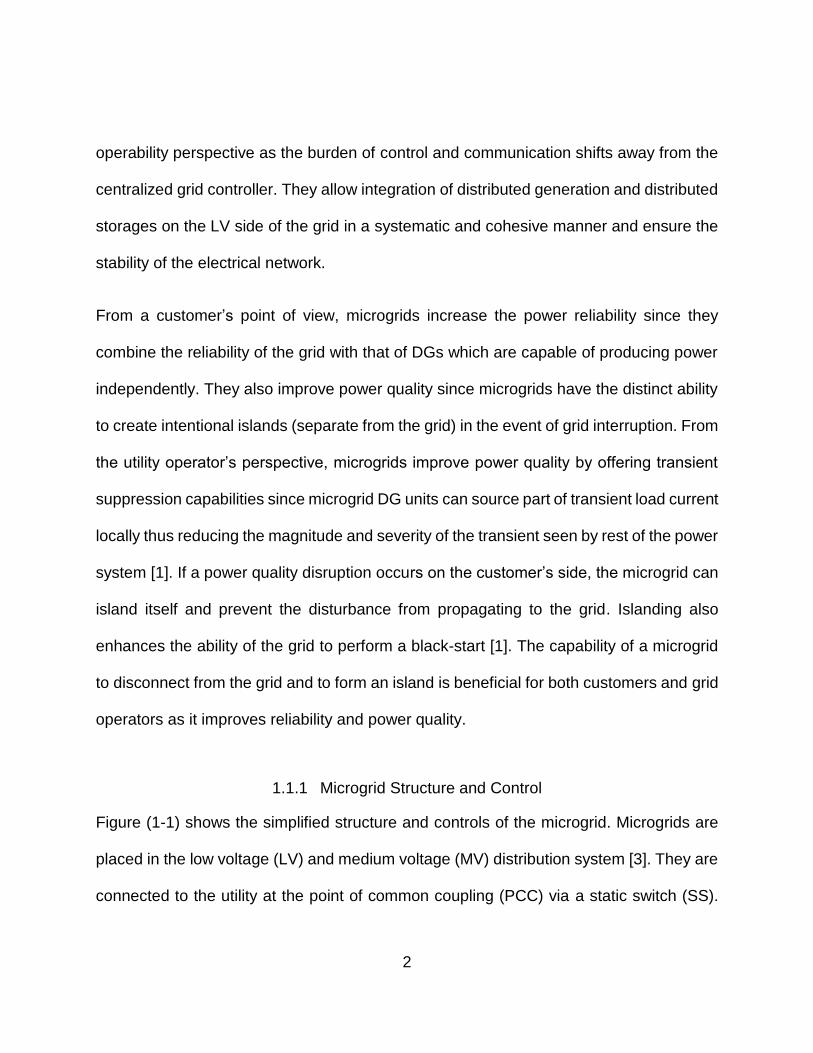
Figure (1-1) shows the simplified structure and controls of the microgrid. Microgrids are
placed in the low voltage (LV) and medium voltage (MV) distribution system [3]. They are
connected to the utility at the point of common coupling (PCC) via a static switch (SS).
3
This switch is controlled by power management unit operated by the microgrid central
controller (MGCC). The Power management unit continuously monitors the voltage and
severe short circuit faults occurring either at the grid end or microgrid end and commands
the static switch to the island the microgrid thus ensuring reliability and stability [5]. The
MGCC sends predefined control signals to the local microsource controller (MC) and load
controller (LC) to perform power balancing and also optimizes microgrid operation based
on electricity market price.
Figure 1-1: Simplified structure and controls of the Microgrid
Microgrids can operate in both grid-connected and islanded mode. In grid-connected
mode, DGs can share loads with the grid. Whereas in the islanded mode, microgrids

4
operate autonomously and interconnected DGs share the load amongst themselves. In
order to maintain stability and operate a microgrid economically, the proper control
structure is required. The principle roles of the Microgrid control structure are voltage and
frequency regulation in both operating modes, accurate load sharing, DG coordination,
microgrid resynchronization with the main-grid, power flow control between main grid and
the microgrid and optimizing the microgrid operating cost [11]. As shown in the figure (1-
1), a microgrid possesses an advanced control structure at different layers to carry out
these functionalities. Each control layer has particular implications and operates at
different rates. This control strategy forms a hierarchical control. The control of a microgrid
can be mainly classified into four levels: local/primary, secondary, central/emergency and
global controls [3]. The local/primary control provides references for the voltage and
current loops operated within the DG unit. These inner level control loops are also known
as zero-level control loops [11] and have a fast-dynamic response. The main function of
this control is to provide voltage and current regulation within the DG unit. Secondary
control has a slower dynamic response compared to the primary control and is mainly
use to compensate for the deviations in the voltage and frequency caused by the primary
control. In secondary control, the microsource controller compares the microgrid
frequency and terminal voltage of the DGs with the reference values and produces error
signals; these error signals are then processed by the frequency, and voltage controllers
and the resulting signals are sent to the primary controller of the DGs to take corrective
measures. Central/emergency control is carried out by MGCC which interfaces between
the MG and other MGs as well as higher distribution network [3]. This control manages

5
power flow between the microgrid and the main grid and is primarily responsible for MG
stability. It is also responsible for taking protective actions in case of power disturbances.
The MGCC communicates with the distribution network and market operator and
optimizes microgrid operation. Central/emergency control is the slowest control that
works on the top level. The global control is a centralized control which allows the MG to
operate at an economic optimum and organizes the relation between the MG and the
distribution network as well as other connected MGs [3].
In this research, the focus is primarily on microsource power limit management performed
by the primary/local control of the microgrid hierarchical control structure. A novel control
technique is developed to carry out power balance between the energy source connected
to the DG and the load.
1.2 Microsources
A DG unit supplies power to the microgrid using energy sources connected to them.
These energy sources are called microsources. A microgrid can consist of a diverse
range of energy sources; it can be renewable energy sources like photovoltaics panels,
wind turbines, fuel cells or can consist of natural gas or fossil fuels. A Microgrid may also
include storage technologies such as batteries, ultra-capacitors and flywheel energy
storage which are interfaced using distributed storage (DS) units. Energy sources can be
connected to the microgrid using either mechanical means (e.g. synchronous generators,
internal combustion engine) or by electrical means; that is by using a power electronics

6
inverter. DG units can be classified into two categories: rotating machine based DGs and
inverter based DGs. This research focuses on inverter based DGs.
The Microsource for an inverter based DG can either source DC power (e.g. Photovoltaic)
or non-utility-grade AC power (e.g. wind-turbine). This power is then converted to utility-
grade AC with the desired magnitude, frequency, and phase angle through the interfacing
power converters [10]. Voltage source inverters (VSI) with sinusoidal-PWM are commonly
used to convert DC power to utility grade AC. DG units with power converters can consist
of one or multiple power processing stages. The type and number of power conversion
stages depends on the nature (DC or AC) of the power source, its capacity, and dynamic
characteristics.
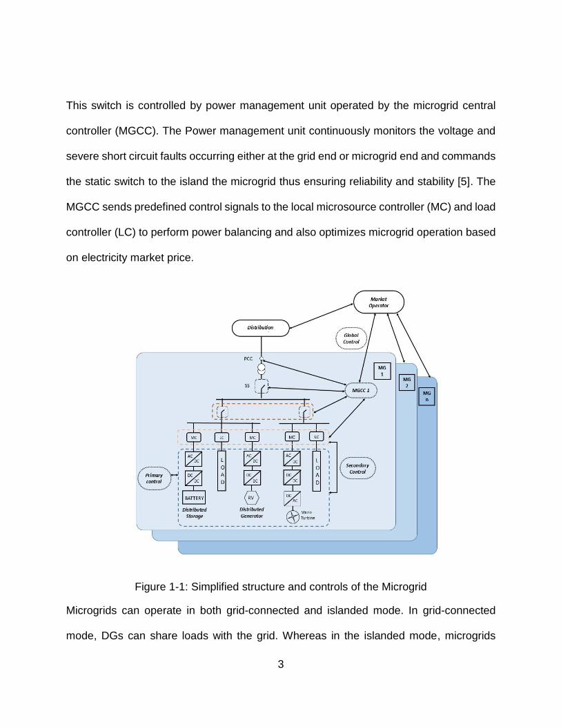
Figure 1-2: Stages of inverter based DG
7
Figure (1-2) shows various power conversion stages in inverter based DG. A single stage
conversion system consists of a microsource (e.g. P.V., battery) directly connected to the
DC-AC inverter stage via a DC-link. In two-stage conversion system, the microsource
(e.g. P.V., battery, Fuel cell) is first connected to DC-DC converter to boost the
microsource output voltage to the desired level and is then connected to DC-AC inverter
stage via the DC-link. In the case of a multi-stage conversion system, the microsource
(e.g. micro-turbine, wind turbine) output is first connected to the AC-DC rectification stage
then to the DC-DC boost stage to bring output voltage to the desired level and finally
connected to DC-AC inverter stage via a DC-link. These power processing configurations
have varying benefits depending upon the microsource.
Inverter-based DGs are further classified into two subgroups depending upon their control
strategies. 1) Grid-forming inverters - this type of inverter control causes their microsource
to behave as a regulated voltage source, and therefore these inverters are capable of
operating in standalone mode. 2) Grid-following inverters - this type of inverter control
causes their microsource to behave as a regulated current source, and requires grid
voltage and frequency as a reference for proper operation [3]. There are three types of
DG units; mechanical/rotating machine based DGs, grid-following based DGs, and grid-
forming based DGs. All of these DGs have a unique dynamic response which
characterizes their behavior in the microgrid. Dynamics of grid-forming based inverters is
covered in section 1.3, dynamics of the grid-following inverters and rotating machine are
8
covered in chapter 2 and chapter 3 respectively. The following section 1.2.1 addresses
the inter-source dynamics of photovoltaic and battery microsources.
1.2.1 Inverters with Photovoltaic Microsource
Using photovoltaic (PV) microsources in the microgrid is popular since it produces clean
energy and has zero fuel cost. Since PV panels do not store energy, it is possible to
rapidly change the output voltage of the PV panel with the help of DC-DC power stage to
track its maximum power point (MPP) and extract maximum power. PV based DG can
consist of an intermediate DC-DC power stage to perform the function of MPP tracking
and boosting the output voltage of PV to the level needed for the inverter power stage.
Both grid-following and grid-forming inverters control techniques can be used to integrate
PV based DGs into a microgrid. PV output power depends on upon incident solar
irradiation and therefore varies slowly. Thus short-term energy required by the load
transient in the case of the grid-forming inverter is only supported by a small capacitor
connected in the inverter stage which acts as a small storage element. The capacitor is
usually sized to provide the instantaneous power difference between DC-DC stage and
inverter stage. Although PV sources have an inherently slow dynamic response and are
usually used with grid-following inverters, they can also act like grid-forming inverters with
small transient support capability.

9
1.2.2 Inverters with Battery Microsource
Batteries are crucial for microgrid operations since they are used as an energy storage in
the microgrid and are categorized as distributed storage (DS). They are capable of
sourcing power above their rating for the brief period provided the RMS power is below
that of continuous power rating [10]. This characteristic allows battery-based inverters to
source the short term energy required by a load transient. Battery based DG units are
usually operated in the grid-forming mode.
Battery-based DGs can consist of intermediate DC-DC stage to boost battery voltage to
the level required for the inverter power stage. Battery based DG usually has a bi-
directional power stage which can charge and discharge the battery as required.
1.3 DG Unit Control Strategies
Inverter based DGs in the microgrid can be either grid-following inverters or grid-forming
inverters depending on their control strategies. Grid-following inverters cannot be
operated independently and require that a voltage source is present on the network. Grid-
forming inverters can be operated in standalone mode as well as grid-connected mode.
For microgrid operation grid-forming inverters are crucial, and their control strategy is
discussed in this chapter. The control strategy of grid-following inverters is discussed in
chapter 2.
The grid-forming inverter’s primary function is to provide voltage and frequency
stabilization, offer plug and play capability to the DGs, accurately share real and reactive
10
power and reduce DC circulating current caused by differences in the voltage magnitude
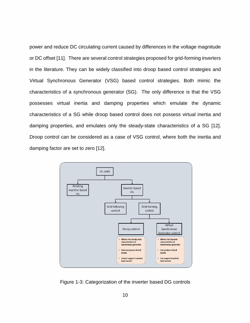
or DC offset [11]. There are several control strategies proposed for grid-forming inverters
in the literature. They can be widely classified into droop based control strategies and
Virtual Synchronous Generator (VSG) based control strategies. Both mimic the
characteristics of a synchronous generator (SG). The only difference is that the VSG
possesses virtual inertia and damping properties which emulate the dynamic
characteristics of a SG while droop based control does not possess virtual inertia and
damping properties, and emulates only the steady-state characteristics of a SG [12].
Droop control can be considered as a case of VSG control, where both the inertia and
damping factor are set to zero [12].
Figure 1-3: Categorization of the inverter based DG controls
11
A VSG control based inverter can supply real power during short-term frequency
transients as well as steady state. Both the control methods are discussed in the following
sections 1.3.1, 1.3.2 and figure (1-3) shows the categorization of these controls.
1.3.1 Droop based Control Strategy
The conventional droop based control method is primarily used for operating DGs in
parallel for microgrid applications. This control method does not require a communication
link between inverters and thus improves reliability and redundancy. Also, such a system
is easier to expand because of the plug and play feature of the module which allows
replacing one unit without stopping the whole system [6]. Droop control emulates the
static characteristics of a SG, i.e. active power is increased with a decrease in system
frequency, and reactive power increases with a decrease in the terminal voltage as shown
in figure (1-4). The principles of conventional droop method can be explained by
considering an equivalent circuit of a VSC connected to an AC bus [11]. Assuming the
VSC is connected to the AC bus using inductive line impedance and negligible resistance,
it can be shown that for small value of power angle 𝛿, real and reactive power output, 𝑃𝑜
and 𝑄𝑜 delivered to common AC bus can be given by equation (1-1).
{ 𝑃𝑜 ≈
|𝑉𝑜|.|𝐸𝑖|.𝛿
𝜔.𝐿𝑠
𝑄𝑜 ≈|𝑉𝑜|.(|𝐸𝑖|−|𝑉𝑜|)
𝜔.𝐿𝑠
( 1-1 )
These equations show that the active power strongly depends on the phase difference (𝛿)
between the inverter output voltage 𝐸𝑖 and AC bus voltage 𝑉𝑜 and reactive power strongly
12
depends on the difference in amplitude of output voltage and AC bus voltage, 𝐸𝑖 and 𝑉𝑜
respectively. This principle can be integrated into the voltage source inverter using well-
known PQ droop method [6] which is expressed by equation (1-2).
{ 𝜔𝑖 = 𝜔0 − 𝑚𝑃. (𝑃𝑖 − 𝑃0)
𝐸𝑖 = 𝐸0 − 𝑛𝑄 . (𝑄𝑖 − 𝑄0) ( 1-2 )
Where 𝜔𝑖 and 𝐸𝑖 are the output frequency and voltage of the ith inverter in the microgrid,
𝜔0 and 𝐸0 are the nominal frequency and voltage of the inverter respectively, 𝑃𝑖 and 𝑄𝑖
are average active and reactive power sensed at the terminal of the inverter, respectively,
and 𝑚𝑃 and 𝑛𝑄 active and reactive droop slopes, respectively. Droop constants 𝑚𝑃 and
𝑛𝑄 affect network stability and are chosen based on converters power rating and
maximum allowable voltage and frequency deviation [11] as shown in equation (1-3)
{ 𝑚𝑃 =
𝜔𝑖,𝑚𝑎𝑥−𝜔0
𝑃𝑖−𝑃𝑖,𝑚𝑎𝑥
𝑛𝑄 =𝐸𝑖,𝑚𝑎𝑥−𝐸0
𝑄𝑖−𝑄𝑖,𝑚𝑎𝑥
( 1-3 )
13
Figure 1-4: Q-E and P-𝜔 Droop control
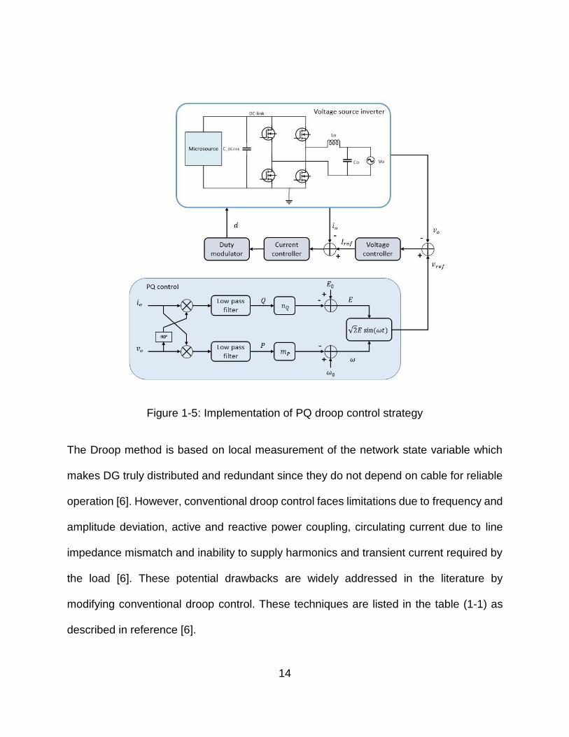
Implementation of the PQ control strategy on a VSI is shown in figure (1-5). This control
strategy delivers active and reactive power based on predetermined references. It
consists of three control structures. 1) PQ controller: This control senses AC bus voltage
and current and produces average P and Q values. These average values are multiplied
by respective droop constants 𝑚𝑃, 𝑛𝑄 and are then are compared with the respective
references 𝜔0, 𝐸0 to produce the reference voltage. 2) Voltage controller: This controller
compares the reference voltage with the actual voltage and produces the current
reference. 3) Current controller: The controller produces the current reference that drives
the voltage source inverter using duty cycle modulator.
14
Figure 1-5: Implementation of PQ droop control strategy
The Droop method is based on local measurement of the network state variable which
makes DG truly distributed and redundant since they do not depend on cable for reliable
operation [6]. However, conventional droop control faces limitations due to frequency and
amplitude deviation, active and reactive power coupling, circulating current due to line
impedance mismatch and inability to supply harmonics and transient current required by
the load [6]. These potential drawbacks are widely addressed in the literature by
modifying conventional droop control. These techniques are listed in the table (1-1) as
described in reference [6].

15
Table 1-1: Droop characteristics based controls
Droop characteristics based controls Advantages over conventional droop
control
Droop variants
VPD/FQB droop
control
To carry out droop control when the transmission line is resistive
Complex line
impedance
Decouples Active and reactive controls
Improves voltage regulation
Virtual structure
based methods
Virtual output
impedance
control
Improves power sharing
Improves system stability
Enhanced virtual
output
impedance
Can handle linear non-linear load
Reduces harmonics voltage at
PCC
Compensated based
methods
Adaptive voltage
droop
control
Improves voltage regulation
Improves system stability under
heavy load
Synchronized
reactive power
compensation
Improves power sharing
1.3.2 Virtual Synchronous Machine Based Control Strategy
This type of grid-forming control is able to emulate the transient characteristics of the SG–
such as damping effects and inertial behavior. These characteristics are embedded in the
16
VSI by different types of VSM topologies and are listed in reference [3]. The emulation of
the inertia requires an energy buffer with sufficient capacity to represent the energy
storage effect [13]. Therefore, when emulating virtual inertia on inverter based DGs, DC-
link energy storage of the inverter acts as a kinetic energy storages reservoir of the SG.
Proper management of DC-link energy storage is crucial for grid-forming inverters since
they provide virtual inertia to the system.
The most common implementation of the VSM model is based on the traditional swing
equation of the SG. Other types of VSM models such as Generator Emulation Control
(GEC) provide an inertial response to variations in grid frequency. GEC is based on
emulating electrical characteristics of a SG in the VSI. In this section, a swing equation
based VSM model is described referring to [3] and the details of GEC model will be
introduced in chapter 2.
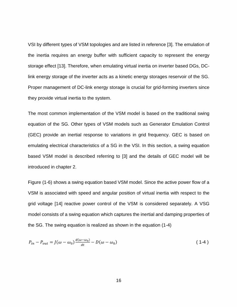
Figure (1-6) shows a swing equation based VSM model. Since the active power flow of a
VSM is associated with speed and angular position of virtual inertia with respect to the
grid voltage [14] reactive power control of the VSM is considered separately. A VSG
model consists of a swing equation which captures the inertial and damping properties of
the SG. The swing equation is realized as shown in the equation (1-4)
𝑃𝑖𝑛 − 𝑃𝑜𝑢𝑡 = 𝐽(𝜔 − 𝜔0)𝑑(𝜔−𝜔0)
𝑑𝑡− 𝐷(𝜔 − 𝜔0) ( 1-4 )
17
Figure 1-6: Implementation of VSG control strategy
Here, 𝑃𝑖𝑛 is the available power from the microsource, 𝑃𝑜𝑢𝑡 is the calculated output power,
𝐽 is the moment of inertia of the rotor, 𝜔 is the angular velocity of the virtual rotor, 𝜔0 is
the grid angular velocity and 𝐷 is the damping factor. Output power and grid angular
velocity is calculated and given as input to the VSG model. The VSG model calculates
virtual rotor angular velocity deviation 𝜔𝑚, which is then integrated to calculate virtual
machine phase angle 𝜃𝑚. As mentioned above, reactive power based voltage calculation
is done separately using PI controller and virtual machine voltage 𝑉𝑚 is obtained. These
two parameters are combined to produce the voltage reference 𝑉𝑟𝑒𝑓 which is then used
by the PWM module to drive the switches.
18
1.4 Power Limit Management for Grid-Forming Inverters.
For the grid-forming inverter, active power is dictated by the droop controller or VSM
based model. Active power (𝑃) is proportional to the deviation of grid frequency (𝜔) from
the nominal frequency the (𝜔0). When the grid-forming inverters are operated in the
islanded microgrid, the deviation of microgrid system frequency will cause the inverter to
source active power. This is the underlying concept of P-𝜔 droop control. When load in
the islanded microgrid increases, the microgrid frequency droops / falls below the nominal
value and this causes the online inverters in the microgrid to source required active power.
The amount of active power inverters can source depends upon their power rating and
the availability of the power form their microsource. If power demanded is higher than the
ability of the inverter to source power, its DC-link voltage decreases. When the DC-link
voltage falls below peak-grid voltage, the inverter tends to over-modulate the DC-link
voltage and produces harmonics which are undesirable. Typically, when DC-link voltage
falls below the predefined value, (usually lower than maximum grid peak voltage) the
inverter protection relay opens, and inverter is isolated from the microgrid network. This
behavior increases power demand on the rest of the inverters connected in the microgrid
and may led to unpredictable load shedding or black-outs. To avoid this situation, DC-link
voltage regulation is essential to power limit the grid-forming inverters and allow them to
continue to source their available power.
In this research, the power-limited nature of the grid-forming inverter is highlighted, and
a DC-link voltage regulation technique is developed for power limit management. This
19
technique is developed on a Generator Emulation Control (GEC) based grid-forming
inverter which gives the inverter an ability to shape its P-𝜔 droop curve and continue to
source power to the load without getting isolated.
1.5 Outline of the Thesis
The primary objective of this thesis is to demonstrate the power limit management or DC-
link voltage regulation of the DG inverters operated in islanded mode. This strategy is
demonstrated on GEC based grid-forming inverter and implemented using virtual
resistance based technique.
Chapter 1 summarized the basic microgrid structure and a hierarchical control at different
layers of MG. It introduced different types of microsources and their dynamics and the
inverter stages. The chapter classified various control strategies for DG inverters and
outlined the difference between droop based control and VSM based control. Finally, it
described the role of power limit management and laid out the importance of DC-link
voltage regulation in DG inverters.
Chapter 2 Introduces the basic controls of the grid-following inverters and explains phase
lock loop (PLL) and output current regulation blocks (OCR). It describes dynamics,
modeling, control design, and implementation of PLL as well as OCR. These blocks are
essential in developing GEC based grid-forming inverters.

20
Chapter 3 summarizes Generator Emulation controls which is one of the control strategies
for grid-forming inverters. It formulates the damping and inertial properties of synchronous
generator and droop controls which form the basis for developing GEC. Later in this
chapter technique to design and implement the GEC control are given.
Chapter 4 summarizes DC-link voltage regulation for grid-following inverters. It brings into
light the importance of DC-link voltage regulation for the safe operation of the DG inverters
and introduces a virtual resistance technique to regulate the DC-link voltage of GEC grid-
forming inverters. A modeling and control design for the DC-link voltage regulator is
developed, and results are presented to demonstrate the concept.
Chapter 5 summarizes the results of the virtual resistance based DC-link voltage
regulation and shows how this technique shapes P-𝜔 droop characteristics of GEC
inverter and carry out power limit management.

21
CHAPTER 2: CONTROLS OF THE GRID-FOLLOWING INVERTERS
Grid-following inverters cannot be operated independently and require a voltage source
to be present on the network. Grid following inverters are also known as grid-tied
inverters. The primary function of grid-following inverters is to source current to the grid
with a power factor close to one. Grid voltage provides frequency and voltage reference
signals to these inverters which are important to perform synchronization and carry out
control functions. The following section introduces basic blocks of the inverter which are
used to carry out synchronization and control functions.
2.1 Basic Blocks of the Inverter
Figure 2-1: Basic Blocks of grid-following inverter
22
Figure (2-1) shows the basic blocks of the grid-following inverter. It consists of an inverter
power stage with phase lock loop (PLL) used for synchronization, an output current
regulator (OCR) and DC-link voltage regulator or Bus Voltage Regulator (BVR) for
regulating output current and DC-link voltage respectively.
1. Phase Lock Loop:
The phase lock loop (PLL) tracks the grid voltage and creates a carrier signal which
synchronizes in phase and frequency with that of the grid voltage. PLL does this by
controlling the phase of the carrier signal such that the phase difference between grid
voltage and carrier signal remains minimum [17]. The advantage of using PLL is that it is
immune to the distortions and amplitude variations of grid voltage and produces high-
quality constant amplitude sinusoidal reference. This sinusoidal reference is scaled by
DC-link voltage regulator loop and later given to OCR loop.
2. Output Current Regulator:
The output Current Regulator is responsible for shaping the output current of the inverter.
OCR regulates output inductor current of the inverter stage. It compares the sensed
inductor current of the inverter with a sinusoidal reference which is the scaled version of
PLL and generates the control signal. This control signal is given to duty modulator block
to generate SPWM signals. Dynamics of OCR loop makes inverter stage behave as a
regulated current source.
23
3. DC-link voltage regulator:
The DC-link voltage regulation loop controls DC-link voltage. DC-link voltage regulator
loop senses DC-link voltage and compares it with the reference DC-link voltage to
produces a slow varying control signal. Value of the DC-link reference is kept slightly
above the peak voltage of the grid and is typically 200 V for 120 𝑉𝑎𝑐 system. Slow varying
control signals modulates the amplitude of the sinusoidal current reference generated by
PLL and is further given to the OCR. DC-link voltage regulator maintains the power
balance between the output power and input available power by controlling the amplitude
of sinusoidal reference given to OCR proportional to DC-link voltage.
2.2 PLL for Grid-following Inverters
This section discusses the PLL structure, modeling and control design for the grid-
following inverter. Properties of PLL are of particular interests as they are used to
reproduce damping and inertial dynamics of the synchronous generator into the GEC
based grid-forming inverters. Even though the PLL structure used for GEC based inverter
is the same as a grid-following inverter, the controller design for PLL employed in GEC
based inverter is different and is highlighted in chapter 3.
24
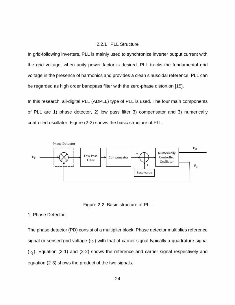
2.2.1 PLL Structure
In grid-following inverters, PLL is mainly used to synchronize inverter output current with
the grid voltage, when unity power factor is desired. PLL tracks the fundamental grid
voltage in the presence of harmonics and provides a clean sinusoidal reference. PLL can
be regarded as high order bandpass filter with the zero-phase distortion [15].
In this research, all-digital PLL (ADPLL) type of PLL is used. The four main components
of PLL are 1) phase detector, 2) low pass filter 3) compensator and 3) numerically
controlled oscillator. Figure (2-2) shows the basic structure of PLL.
Figure 2-2: Basic structure of PLL
1. Phase Detector:
The phase detector (PD) consist of a multiplier block. Phase detector multiplies reference
signal or sensed grid voltage (𝑣𝑜) with that of carrier signal typically a quadrature signal
(𝑣𝑞). Equation (2-1) and (2-2) shows the reference and carrier signal respectively and
equation (2-3) shows the product of the two signals.

25
𝑣𝑜(𝑡) = 𝐴1 cos(𝜔𝑡 + 𝜙1(𝑡)) ( 2-1 )
𝑣𝑞(𝑡) = 𝐴2 sin(𝜔𝑡 + 𝜙2(𝑡)) ( 2-2 )
𝑣𝑜(𝑡). 𝑣𝑞(𝑡) = 𝐴1. 𝐴2. 𝐾𝑑[sin(𝜙1(𝑡) − 𝜙2(𝑡)) + sin(2𝜔𝑡 + 𝜙1(𝑡) + 𝜙2(𝑡))] ( 2-3 )
Where, 𝐾𝑑 is the gain of multiplier and its value is 0.5. 𝐴1 and 𝐴2 are the amplitude of
reference and quadrature signal respectively and are scaled to unity. It can be seen form
equation (2-3) that multiplier output consists of two terms, the first term is the function of
phase difference and second term consists of twice the frequency. The useful information
regarding phase difference resides in the first term and, high frequency term is removed
using low pass filter.
2. Low pass filter:
A low pass filter (LPF) is used to remove twice the frequency term 2𝜔𝑡. Since the
frequency of the reference signal (grid voltage) is 60 Hz, 2𝜔𝑡 has the frequency of 120Hz.
This component is attenuated using low pass filter with sufficiently small cutoff frequency.
The output of Low pass filter is the error signal which contains the phase difference
information.
3. Compensator:
The compensator is employed to reduce the phase difference between the reference
signal and the carrier signal to zero. PI compensator is usually used to achieve this task.

26
PI compensator is designed to achieve zero steady-state error and fast transient
response by appropriately choosing crossover frequency and phase margin. The output
of compensator is correction signal which is given as an input to the numerically controlled
oscillator.
4. Numerically Controlled Oscillator:
The numerically controlled oscillator (NCO) produces periodic signals, the frequency of
which changes based on a control signal applied externally [16]. The input to the NCO is
a correction signal from compensator added with base signal. The base signal in case of
NCO is a numerical value which is responsible for producing a center frequency of 60Hz.
Output of NCO consists of direct term (𝑣𝑑) which is in phase with reference voltage and
quadrature term (𝑣𝑞) which is 90° phase shifted with respect to reference signal. Both of
these terms are categorized as carrier signals. In this case, since multiplier type phase
detector is employed, 𝑣𝑞 term is compared with the reference signal so that it gives phase
difference term. In other words, 𝑣𝑞 term is considered as a feedback signal.
2.2.2 PLL Modeling and Control Design
PLL controls the phase of its carrier signal such that the error, the difference between its
phase and the input signal is kept minimum while the frequency of its signal is kept the
same as the input signal [16]. Correction signal from compensator causes the frequency
of carrier signal generated by NCO to change; this change is translated as a change in
phase at the output of phase detector. Thus, PLL can be thought of the perceiving only
27
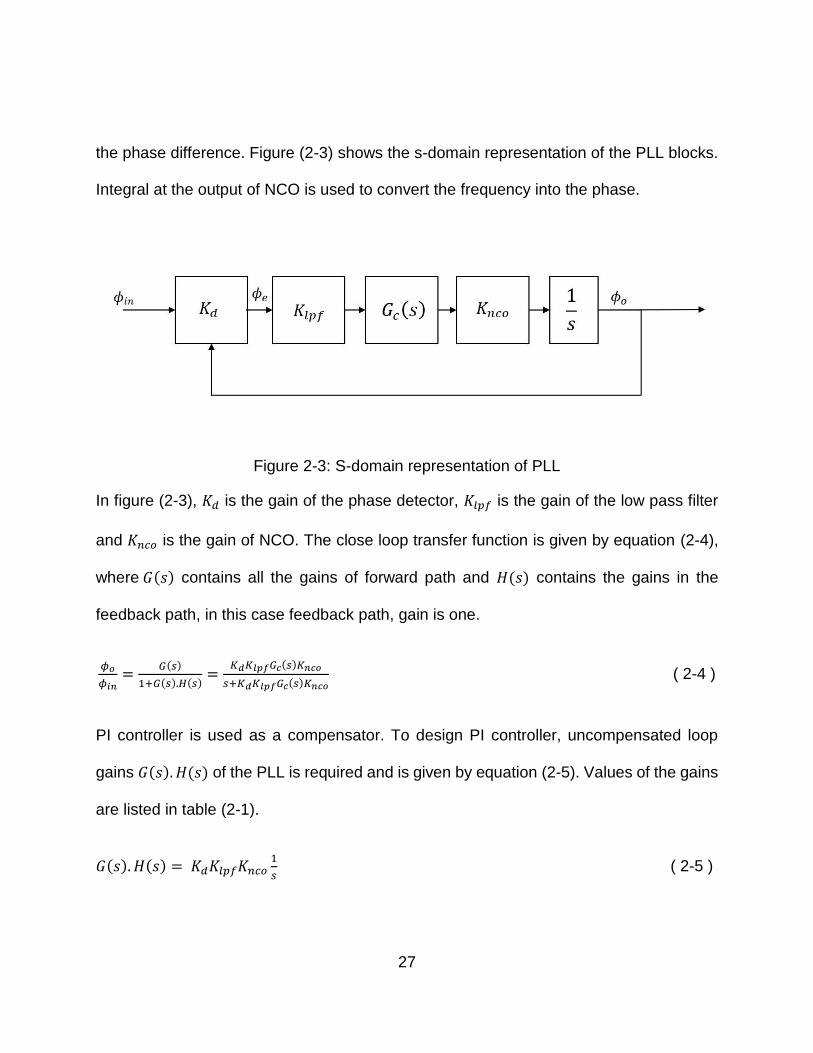
the phase difference. Figure (2-3) shows the s-domain representation of the PLL blocks.
Integral at the output of NCO is used to convert the frequency into the phase.
Figure 2-3: S-domain representation of PLL
In figure (2-3), 𝐾𝑑 is the gain of the phase detector, 𝐾𝑙𝑝𝑓 is the gain of the low pass filter
and 𝐾𝑛𝑐𝑜 is the gain of NCO. The close loop transfer function is given by equation (2-4),
where 𝐺(𝑠) contains all the gains of forward path and 𝐻(𝑠) contains the gains in the
feedback path, in this case feedback path, gain is one.
𝜙𝑜
𝜙𝑖𝑛=
𝐺(𝑠)
1+𝐺(𝑠).𝐻(𝑠)=
𝐾𝑑𝐾𝑙𝑝𝑓𝐺𝑐(𝑠)𝐾𝑛𝑐𝑜
𝑠+𝐾𝑑𝐾𝑙𝑝𝑓𝐺𝑐(𝑠)𝐾𝑛𝑐𝑜 ( 2-4 )
PI controller is used as a compensator. To design PI controller, uncompensated loop
gains 𝐺(𝑠). 𝐻(𝑠) of the PLL is required and is given by equation (2-5). Values of the gains
are listed in table (2-1).
𝐺(𝑠). 𝐻(𝑠) = 𝐾𝑑𝐾𝑙𝑝𝑓𝐾𝑛𝑐𝑜1
𝑠 ( 2-5 )
28
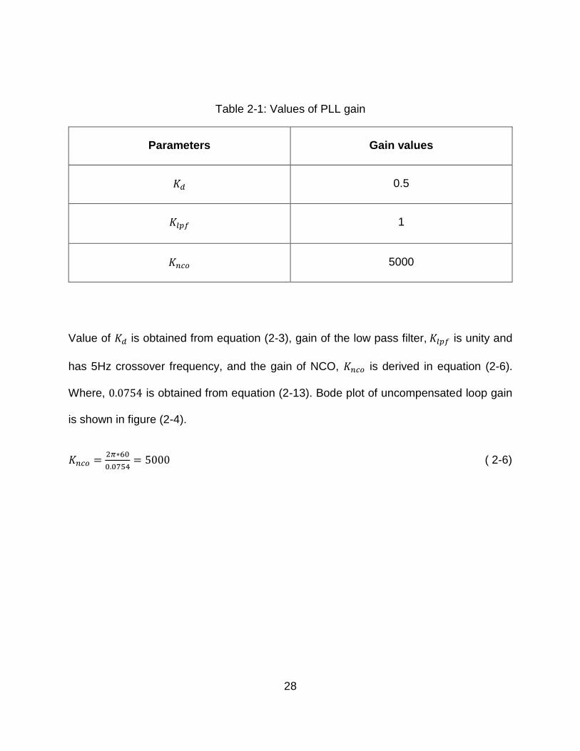
Table 2-1: Values of PLL gain
Parameters Gain values
𝐾𝑑 0.5
𝐾𝑙𝑝𝑓 1
𝐾𝑛𝑐𝑜 5000
Value of 𝐾𝑑 is obtained from equation (2-3), gain of the low pass filter, 𝐾𝑙𝑝𝑓 is unity and
has 5Hz crossover frequency, and the gain of NCO, 𝐾𝑛𝑐𝑜 is derived in equation (2-6).
Where, 0.0754 is obtained from equation (2-13). Bode plot of uncompensated loop gain
is shown in figure (2-4).
𝐾𝑛𝑐𝑜 =2𝜋∗60
0.0754= 5000 ( 2-6)
29
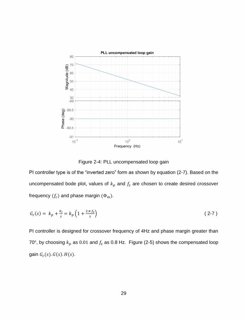
Figure 2-4: PLL uncompensated loop gain
PI controller type is of the “inverted zero” form as shown by equation (2-7). Based on the
uncompensated bode plot, values of 𝑘𝑝 and 𝑓𝑧 are chosen to create desired crossover
frequency (𝑓𝑐) and phase margin (Φ𝑚).
𝐺𝑐(𝑠) = 𝑘𝑝 +𝑘𝑖
𝑠= 𝑘𝑝 (1 +
2.𝜋.𝑓𝑧
𝑠) ( 2-7 )
PI controller is designed for crossover frequency of 4Hz and phase margin greater than
70°, by choosing 𝑘𝑝 as 0.01 and 𝑓𝑧 as 0.8 Hz. Figure (2-5) shows the compensated loop
gain 𝐺𝑐(𝑠). 𝐺(𝑠). 𝐻(𝑠).
30
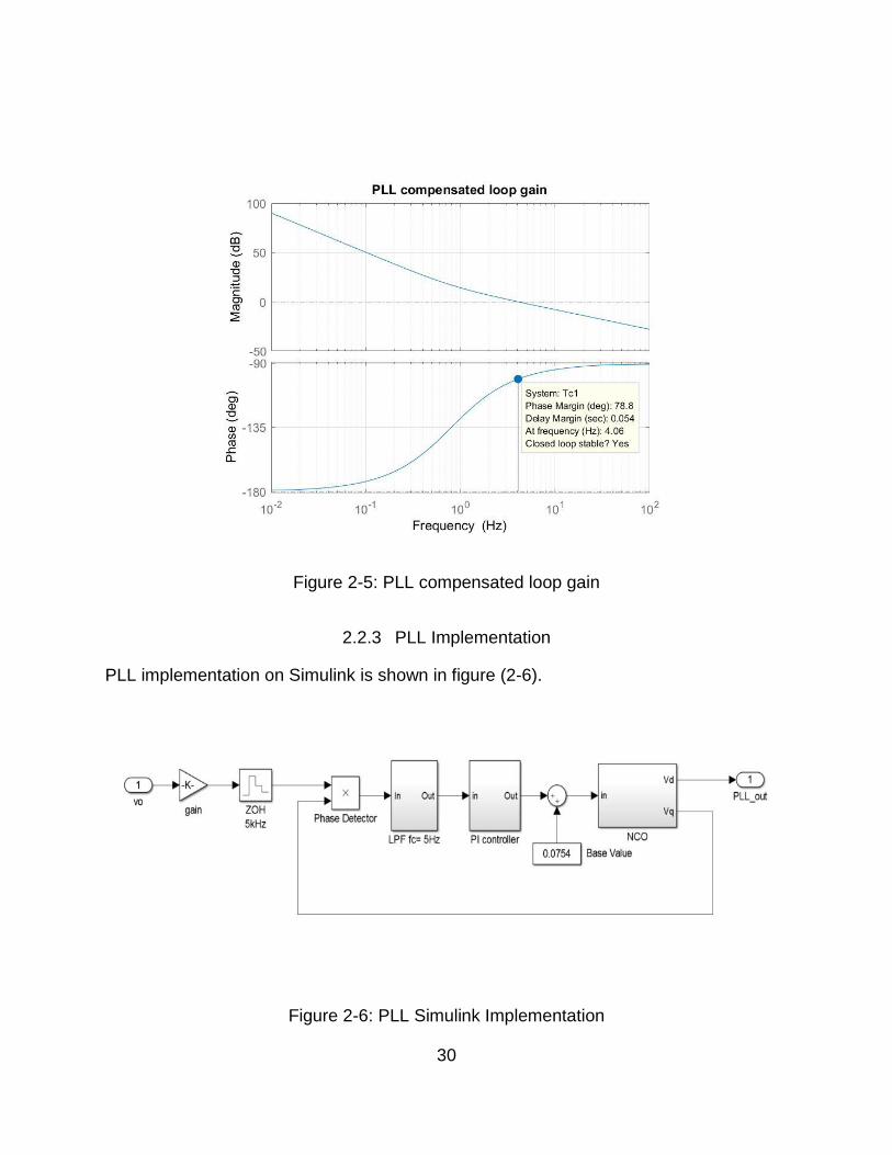
Figure 2-5: PLL compensated loop gain
2.2.3 PLL Implementation
PLL implementation on Simulink is shown in figure (2-6).
Figure 2-6: PLL Simulink Implementation

31
1. Gain block:
Gain block is used to scale down grid voltage to ±1V.
2. ZOH block:
ZOH is used to samples the scaled grid voltage, 𝑣𝑜 at 5KHz sampling rate.
3. Phase detector:
Phase detector is simply a multiplier block which multiplies sampled 𝑣𝑜 with quadrature
component 𝑣𝑞.
4. Low pass filter:
Required crossover frequency (𝑓𝑐) is 5Hz with gain (𝐺) of unity and sampling frequency
(𝑓𝑠𝑎𝑚𝑝𝑙𝑒) is 5kHz. Digital IIR low pass filter is given by the form shown in equation (2-8).
𝐻(𝑧) =𝑏0
1+(𝑏0−1).𝑧−1 ( 2-8 )
Where, 𝑏0 =𝐺
𝜏.𝑓𝑠𝑎𝑚𝑝𝑙𝑒 and 𝜏 =
1
2𝜋.𝑓𝑐
Substituting values in equation (2-8), we get equation (2-9).
𝐻(𝑧) =0.006283
1−(0.993717).𝑧−1 ( 2-9 )
32
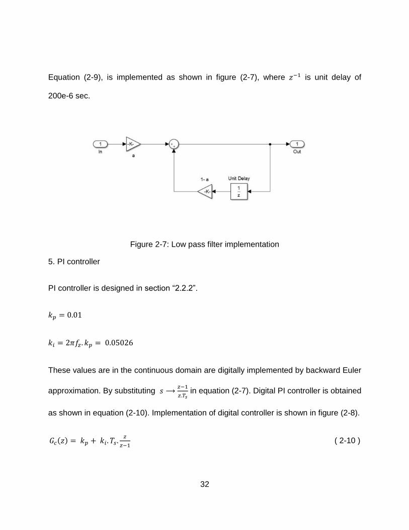
Equation (2-9), is implemented as shown in figure (2-7), where 𝑧−1 is unit delay of
200e-6 sec.
Figure 2-7: Low pass filter implementation
5. PI controller
PI controller is designed in section “2.2.2”.
𝑘𝑝 = 0.01
𝑘𝑖 = 2𝜋𝑓𝑧 . 𝑘𝑝 = 0.05026
These values are in the continuous domain are digitally implemented by backward Euler
approximation. By substituting 𝑠 ⟶𝑧−1
𝑧.𝑇𝑠 in equation (2-7). Digital PI controller is obtained
as shown in equation (2-10). Implementation of digital controller is shown in figure (2-8).
𝐺𝑐(𝑧) = 𝑘𝑝 + 𝑘𝑖. 𝑇𝑠.𝑧
𝑧−1 ( 2-10 )

33
𝑘𝑝_𝑑𝑖𝑔𝑖𝑡𝑎𝑙 = 0.01
𝑘𝑖_𝑑𝑖𝑔𝑖𝑡𝑎𝑙 = 2. 𝜋. 𝑓𝑧 . 𝑘𝑝_𝑑𝑖𝑔𝑖𝑡𝑎𝑙 . 𝑇𝑠 = 0.05026 (1
5𝑘𝐻𝑧) = 0.01005𝑒 − 3
These gains are implemented with a negative sign to correct the phase of the direct
component at the output of NCO.
Figure 2-8: Digital PI-controller implementation
6. Numerically controlled oscillator
NCO is based on the theory of complex number multiplication. Complex number can be
represented by two-dimensional vector, 𝑅𝑒[𝑛] + 𝒋 𝐼𝑚[𝑛].
Where, 𝑀𝑎𝑔𝑛𝑖𝑡𝑢𝑑𝑒 = √𝑅𝑒[𝑛]2 + 𝐼𝑚[𝑛]2 and 𝑎𝑛𝑔𝑙𝑒 = tan−1 (𝐼𝑚[𝑛]
𝑅𝑒[𝑛])

34
Multiplication of two polar complex number results into multiplication of magnitude and
addition of angles. This property is critical in building complex number based oscillator.
This property is shown in equation (2-11)
(𝑀1∠𝜃1)(𝑀2∠𝜃2) = (𝑀1𝑀2) ∠(𝜃1 + 𝜃2) ( 2-11 )
For 5kHz sampling rate, number of samples that can represent one entire cycle of 60Hz
is given by equation (2-12)
𝑠𝑎𝑚𝑝𝑙𝑒𝑠 =𝑓𝑠𝑎𝑚𝑝𝑙𝑖𝑛𝑔
𝑓𝑐𝑦𝑐𝑙𝑒=
50𝑘𝐻𝑧
60𝐻𝑧= 83.33 ( 2-12 )
In polar coordinate form to cover entire unit circle using 83.33 samples, angle requirement
can be given by equation (2-13)
𝑎𝑛𝑔𝑙𝑒 =2𝜋
𝑠𝑎𝑚𝑝𝑙𝑒=
2𝜋
83.33= 0.0754 ( 2-13 )
If the angle of 0.0754 is accumulated in an array with a sampling frequency of 5kHz, the
entire cycle of 60Hz can be formed in 83.33 samples. For implementation, complex
numbers in rectangular form are much easier to operate as they can be represented in
an array. The same property as mentioned in equation (2-11) can be duplicated in
complex numbers in rectangular form, by multiplying them with their previous value and
considering the initial value of real part as one.
Equation (2-14) shows the multiplication of complex number with its previous value.
Where ‘n’ represents present value in the array.

35
{𝑅𝑒[𝑛] + 𝒋 𝐼𝑚[𝑛]} . {𝑅𝑒[𝑛 − 1] + 𝒋 𝐼𝑚[𝑛 − 1]} ( 2-14 )
In equation (2-14), by substituting initial conditions; 𝑅𝑒[𝑛 − 1] = 1 and 𝐼𝑚[𝑛 − 1] = 0 and
keeping value of 𝐼𝑚[𝑛] 0.0754 and value of 𝑅𝑒[𝑛] as cos (0.0754) i.e. 0.9971,
consecutive multiplication with previous complex number, produces cosine function in
𝑅𝑒[𝑛] array and sin function in 𝐼𝑚[𝑛] array. This forms the oscillator and is shown in figure
(2-9). To maintain the sustained oscillations, magnitude of real part is compensated using
a simple proportional controller. Input (in) is base value 0.0754 plus the correction signal.
Figure 2-9: Implementation of NCO
2.3 OCR for Grid-following Inverter
Grid-following or grid-tied inverters are designed to inject current into the grid. Typically,
the single current control loop is employed to regulate the flow of current into the grid [7].
OCR is of specific interest as its design and implementation remain the same for both

36
grid-following and GEC based inverters. Dynamics, modeling and control design of OCR
are discussed in this section.
2.3.1 OCR Dynamics
Figure 2-10: Output current regulator loop model
Figure (2-10) shows the model of inverter with current controller 𝐺𝑐(𝑠). In the frequency
range of concern, the loop frequency response can be approximated by equation (2-15)
[1].
𝐿𝑜𝑜𝑝𝑂𝐶𝑅(𝑠) =𝜔𝑐
2
𝑠2 ( 2-15 )
Where 𝜔𝑐 is crossover frequency which determines the bandwidth of the controller and is
based upon the controller parameters 𝐺𝑐(𝑠) and plant dynamics. Transfer function of the
inductor output current 𝑖𝐿𝑜(𝑠) to the grid voltage 𝑣𝑜(𝑠) can be derived by equation (2-16)
[1].

37
𝑖𝑙𝑜(𝑠)
𝑣𝑜(𝑠)=
−1 𝑠 . 𝐿𝑜⁄
1+𝐿𝑜𝑜𝑝𝑂𝐶𝑅(𝑠)=
−1
𝑠 . 𝐿𝑜 .
−1
1+𝜔𝑐2 𝑠2⁄
( 2-16 )
In the frequency range of interest, it can be further approximated by equation (17) [1]
𝑖𝑙𝑜(𝑠)
𝑣𝑜(𝑠)=
−𝑠2 𝜔𝑐2⁄
𝑠 . 𝐿𝑜 =
−𝑠
𝜔𝑐2 . 𝐿𝑜
( 2-17 )
The inductor current induced by the grid voltage 𝑣𝑜 resembles that flowing in a “virtual
capacitor” connected across it of the value given by equation (18) [1].
𝐶𝑜𝑐𝑟 =−𝑠
𝜔𝑐2 . 𝐿𝑜
( 2-18 )
In addition, with 𝐶𝑜𝑐𝑟 capacitor inverter output filter has small capacitor 𝐶𝑜, thus the
resultant capacitor at the output on the inverter can be given by equation (2-19)
𝐶𝑡𝑜𝑡𝑎𝑙 = 𝐶𝑜𝑐𝑟 + 𝐶𝑜 ( 2-19)
The value of 𝐶𝑜𝑐𝑟 depends upon crossover frequency, ideally cross over frequency is
chosen as 10 % to 20 % of that of switching frequency [7]. In case of the inverter
connected to the infinite bus, grid voltage 𝑣𝑜 acts as infinite current sink and can be
modeled as a short circuit, this causes capacitor connected at the output of the inverter
to open, and not contribute to OCR dynamics. In case of inverter connected to the electric
power system, 𝑣𝑜 can have some impedance and the inverter output capacitor contribute
to the OCR dynamics. For GEC based inverter, dynamics of these capacitors are
considered to prevent sustained oscillations and resonance above line.

38
2.3.2 OCR Plant Modeling and Controller Design
Figure 2-11: Inverter stage model for developing 𝐺𝑖𝑑(𝑠)
For designing current controller, inductor current to control 𝐺𝑖𝑑(𝑠) transfer function is
required. This transfer function is derived using figure (2-11) which consists of inverter
output filter connected in between inverter voltage �̂�. 𝑉𝑑𝑐−𝑙𝑖𝑛𝑘 and the grid voltage 𝑣𝑜 .
Inverter output filter comprises of output inductor 𝐿𝑜 with resistance 𝑅𝑜 and output
capacitor 𝐶𝑜.
Since the dynamics of the OCR loop are developed to make inverter behave as a
regulated current source, the grid impedance (𝑍𝑔𝑟𝑖𝑑) can be modeled as zero. Short circuit
across the capacitor makes it open and inductor current to control 𝐺𝑖𝑑(𝑠) transfer function
can be given by equation (2-20).
𝐺𝑖𝑑(𝑠) =𝑖𝑙�̂�
�̂�=
𝑉𝑑𝑐−𝑙𝑖𝑛𝑘
𝑠.𝐿𝑜𝑅𝑜 ( 2-20 )

39
Figure 2-12: Output current regulator with PI and feedforward control
Current controller 𝐺𝑐(𝑠) is designed based on 𝐺𝑖𝑑(𝑠), and is chosen as proportional
integral (PI) with feedforward (FF) as shown in figure (2-12), where 𝐻 is the current sensor
gain. PI+FF has faster transient response and converges to desire value with no steady-
state error compared to the PI-only type of controller [7]. Equation (2-21) shows the close
loop transfer function of OCR with PI+FF controller. It shows that the inductor current 𝑖𝐿
is only influenced by 𝑖𝑟𝑒𝑓 term as grid voltage 𝑣𝑜 term cancels out by the addition of feed
forward term. PI+FF controller, 𝐺𝑐 for the inverter stage is designed based on system
parameters listed in table (2-2).
𝑖𝑙 =𝐺𝑐.𝑉𝑑𝑐−𝑙𝑖𝑛𝑘 𝑠.𝐿𝑜⁄
1+𝐻.𝐺𝑐 .𝑉𝑑𝑐−𝑙𝑖𝑛𝑘 𝑠.𝐿𝑜⁄𝑖𝑟𝑒𝑓 −
1 𝑠.𝐿𝑜⁄
1+𝐻.𝐺𝑐 . 𝑉𝑑𝑐−𝑙𝑖𝑛𝑘 𝑠.𝐿𝑜⁄𝑣𝑜 +
𝑉𝑑𝑐−𝑙𝑖𝑛𝑘.1 𝑠.𝐿𝑜⁄
1+𝐻.𝐺𝑐 . 𝑉𝑑𝑐−𝑙𝑖𝑛𝑘 𝑠.𝐿𝑜⁄𝑉𝑑𝑐−𝑙𝑖𝑛𝑘
−1. 𝑣𝑜 ( 2-21 )

40
Table 2-2: System parameters for designing OCR
Parameters Values
Power level (𝑃) 200 V
Grid voltage (𝑣𝑜) 120 𝑉𝑟𝑚𝑠
Grid Frequency (𝑓𝑜) 60 Hz
DC-link voltage (𝑉𝑏𝑢𝑠) 200 V
Output inductor (𝐿𝑜) 3.55 mH
Output inductor resistance (𝑅𝑜) 0.273 Ohms
Switching frequency (𝑓𝑠𝑤) 20 kHz
Current sensor gain (𝐻) 0.8
PI controller type is of the “inverted zero” form as shown in equation (2-22). To design PI
controller, uncompensated loop gain 𝐺𝑖𝑑(𝑠). 𝐻(𝑠) is first plotted as shown in figure (2-13).
Based on the bode plot values of 𝑘𝑝 and 𝑓𝑧 are chosen to create desired cross over
frequency (𝑓𝑐) and phase margin (Φ𝑚).
41
𝐺𝑐(𝑠) = 𝑘𝑝 +𝑘𝑖
𝑠= 𝑘𝑝 (1 +
2.𝜋.𝑓𝑧
𝑠) ( 2-22 )
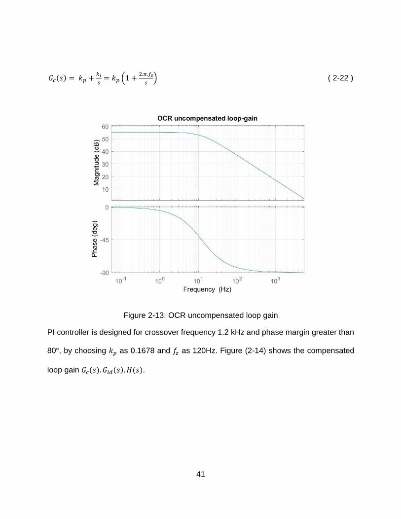
Figure 2-13: OCR uncompensated loop gain
PI controller is designed for crossover frequency 1.2 kHz and phase margin greater than
80°, by choosing 𝑘𝑝 as 0.1678 and 𝑓𝑧 as 120Hz. Figure (2-14) shows the compensated
loop gain 𝐺𝑐(𝑠). 𝐺𝑖𝑑(𝑠). 𝐻(𝑠).
42
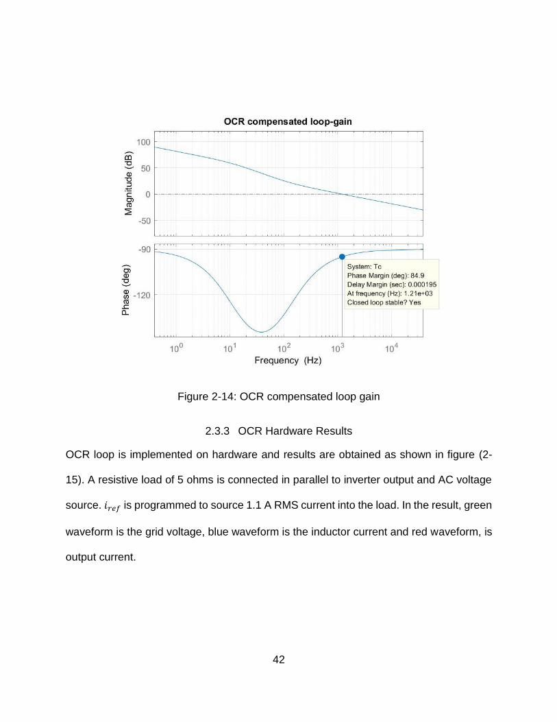
Figure 2-14: OCR compensated loop gain
2.3.3 OCR Hardware Results
OCR loop is implemented on hardware and results are obtained as shown in figure (2-
15). A resistive load of 5 ohms is connected in parallel to inverter output and AC voltage
source. 𝑖𝑟𝑒𝑓 is programmed to source 1.1 A RMS current into the load. In the result, green
waveform is the grid voltage, blue waveform is the inductor current and red waveform, is
output current.
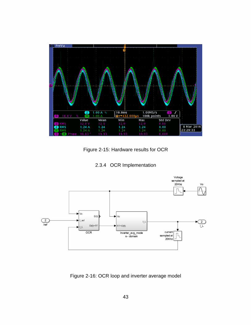
43
Figure 2-15: Hardware results for OCR
2.3.4 OCR Implementation
Figure 2-16: OCR loop and inverter average model
44
OCR implementation on Simulink is shown in figure (2-16). It consists of an average
model of the inverter and OCR loop. In averaged inverter model, duty modulator is not
required, and output of OCR can be directly fed. OCR loop functions and updates duty at
20kHz frequency. Sensed voltage and current are also sampled at 20kHz frequency.
1. Inverter average model
Inverter average model consists of the implementation of the model shown in figure
(2-10), without the output capacitor. Inductor current is obtained by integrating voltage
across it and dividing it by value of inductance. Implementation of averaged inverter
model is shown in figure (2-17).
Figure 2-17: Inverter average model
2. OCR loop
PI controller for OCR is designed in section “2.3.2”.𝑘𝑝 = 0.1678 𝑘𝑖 = 2𝜋𝑓𝑧 . 𝑘𝑝 = 126.518

45
OCR loop compares reference current with actual inductor current and gives an error to
PI controller. PI is implemented digitally using backward Euler approximation. By
substituting 𝑠 ⟶𝑧−1
𝑧.𝑇𝑠 in equation (2-22). Digital PI controller is obtained as shown in
equation (2-23).
𝐺𝑐(𝑧) = 𝑘𝑝 + 𝑘𝑖. 𝑇𝑠.𝑧
𝑧−1 ( 2-23 )
𝑘𝑝_𝑑𝑖𝑔𝑖𝑡𝑎𝑙 = 0.1678
𝑘𝑖_𝑑𝑖𝑔𝑖𝑡𝑎𝑙 = 2. 𝜋. 𝑓𝑧 . 𝑘𝑝_𝑑𝑖𝑔𝑖𝑡𝑎𝑙 . 𝑇𝑠 = 126.518 (1
20𝑘𝐻𝑧) = 6.3259𝑒 − 3
𝑘𝑝_𝑑𝑖𝑔𝑖𝑡𝑎𝑙 and 𝑘𝑖_𝑑𝑖𝑔𝑖𝑡𝑎𝑙 are used in PI controller implementation. Output of PI controller is
then added with feedforward output voltage. FF term reduces the effect of the output
voltage on the inductor current and keeps duty small avoiding integral saturation. D(t)+FF
term is then fed to average inverter model. OCR loop implementation in shown in figure
(2-18).

46
Figure 2-18: OCR implementation
47
CHAPTER 3: GENERATOR EMULATION CONTROL FOR THE INVERTERS
Generator Emulation Control (GEC) is the type of VSM strategy which emulates inertia
and damping characteristic of the synchronous generator into the inverter. GEC
reproduces electrical characteristic of the synchronous generator using “virtual emulation”
technique. This technique incorporates virtual components into the inverter using
computation method.
Among all the VSM strategies, Generator Emulation Control (GEC), encompasses a
practical and robust approach to address grid instability problems by creating a virtual
inertia into the power system. Inverters with GEC support voltage regulation by sourcing
/ sinking reactive power and frequency regulation with the help of power-frequency droop
controls embedded in GEC. Droop properties can also be used by inverters with GEC to
mimic the parallel-operation characteristics of synchronous generators which are
responsible for load sharing [4]. GEC also considers the power-limited nature of DG
sources like battery capacity, battery state of charge, available power from renewable
energies as well as the power rating of the inverter and their effect on DC link voltage [1].
All these capabilities make GEC based inverter truly holistic in practical scenarios.
In this chapter dynamic properties of the synchronous generator are discussed, and
equations for their inertial and damping properties are derived. These properties are then
programmed into the inverter with the help of “virtual emulation technique” and “droop-
based PLL.”

48
3.1 Dynamic Properties of Synchronous Generator
Figure 3-1: Basic block of power generator system
Figure (3-1) shows the basic blocks of a power generator system. The power generator
system consists of an energy source, prime mover, and a synchronous generator. The
energy source supplies fuel to the prime mover which converters the fuel energy into the
rotational kinetic energy. This rotational kinetic energy is further used to drive the rotor of
the synchronous generator. The synchronous generator is electro-mechanical machines
which converters mechanical energy to the electrical energy. Governor and Automatic
Voltage Regulator (AVR) are the controllers used to maintain generator output frequency
and voltage respectively. The Governor connected to the prime mover regulates its
rotational speed based on the power demand. The AVR monitors generator terminal
voltage and sends correction commands to exciter which then adjusts rotor field current
49
to maintain the terminal voltage. In the case of thermal power plant, the energy source
can consist of fossil fuel, nuclear reactor, geothermal resources, renewable resources,
etc. and prime mover can include steam turbine, gas turbine, internal combustion engine,
microturbine, etc.
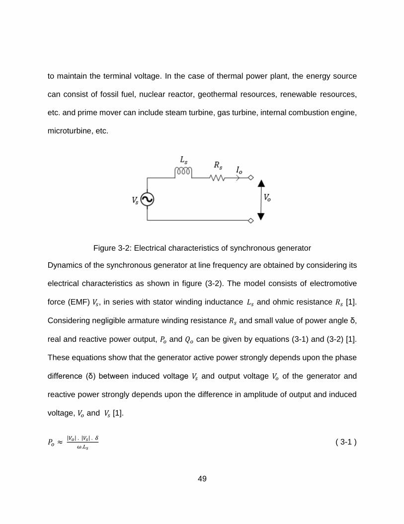
Figure 3-2: Electrical characteristics of synchronous generator
Dynamics of the synchronous generator at line frequency are obtained by considering its
electrical characteristics as shown in figure (3-2). The model consists of electromotive
force (EMF) 𝑉𝑠, in series with stator winding inductance 𝐿𝑠 and ohmic resistance 𝑅𝑠 [1].
Considering negligible armature winding resistance 𝑅𝑠 and small value of power angle δ,
real and reactive power output, 𝑃𝑜 and 𝑄𝑜 can be given by equations (3-1) and (3-2) [1].
These equations show that the generator active power strongly depends upon the phase
difference (δ) between induced voltage 𝑉𝑠 and output voltage 𝑉𝑜 of the generator and
reactive power strongly depends upon the difference in amplitude of output and induced
voltage, 𝑉𝑜 and 𝑉𝑠 [1].
𝑃𝑜 ≈ |𝑉𝑜| . |𝑉𝑠| . 𝛿
𝜔.𝐿𝑠 ( 3-1 )
50
𝑄𝑜 ≈ |𝑉𝑜| . (|𝑉𝑠|−|𝑉𝑜|)
𝜔.𝐿𝑠 ( 3-2 )
Frequency of induced EMF 𝜔𝑠 is determined by rotational speed of rotor and construction
of machine, and is given by equation (3-1), where 𝑛 is number of poles and 𝜔𝑚𝑒𝑐ℎ is the
mechanical rotational speed of the rotor [1].
𝜔𝑠 = 𝑛 . 𝜔𝑚𝑒𝑐ℎ ( 3-3 )
However, the voltage amplitude of the induced EMF |𝑉𝑠| is proportional to the rotor flux 𝜙
and operational frequency [1] and is given by equation (3-4).
|𝑉𝑠| ∝ 𝜔𝑚𝑒𝑐ℎ . 𝜙 ( 3-4 )
Rotational kinetic energy is stored in the rotating mass of the generator system, i.e. prime
mover, and synchronous machine rotor. This kinetic energy is given by equation (3-5),
where 𝐸𝑘𝑖𝑛𝑒𝑡𝑖𝑐 is kinetic energy and 𝐽 is moment of inertia of rotating mass.
𝐸𝑘𝑖𝑛𝑒𝑡𝑖𝑐 =1
2 . 𝐽 . 𝜔𝑚𝑒𝑐ℎ
2 ( 3-5 )
Rate of change of kinetic energy 𝐸𝑘𝑖𝑛𝑒𝑡𝑖𝑐 is equivalent to difference between prime mover
power input (𝑃𝑖𝑛) and electrical power output (𝑃𝑜) neglecting any losses [1]. Substituting
equation (3-3) into equation (3-5) gives equation (3-7).
𝜔𝑠 =𝑛2
𝐽 . 𝜔𝑠̅̅ ̅̅ . ∫(𝑃𝑖𝑛 − 𝑃𝑜) . 𝑑𝑡 ( 3-6 )
𝜔𝑠 = 𝑘𝑟𝑜𝑡𝑜𝑟 . ∫(𝑃𝑖𝑛 − 𝑃𝑜) . 𝑑𝑡 ( 3-7 )
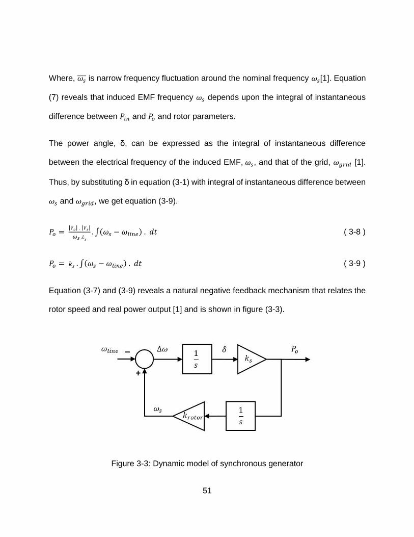
51
Where, 𝜔𝑠̅̅ ̅ is narrow frequency fluctuation around the nominal frequency 𝜔𝑠[1]. Equation
(7) reveals that induced EMF frequency 𝜔𝑠 depends upon the integral of instantaneous
difference between 𝑃𝑖𝑛 and 𝑃𝑜 and rotor parameters.
The power angle, δ, can be expressed as the integral of instantaneous difference
between the electrical frequency of the induced EMF, 𝜔𝑠, and that of the grid, 𝜔𝑔𝑟𝑖𝑑 [1].
Thus, by substituting δ in equation (3-1) with integral of instantaneous difference between
𝜔𝑠 and 𝜔𝑔𝑟𝑖𝑑, we get equation (3-9).
𝑃𝑜 = |𝑉𝑜| . |𝑉𝑠|
𝜔𝑠 .𝐿𝑠
. ∫(𝜔𝑠 − 𝜔𝑙𝑖𝑛𝑒) . 𝑑𝑡 ( 3-8 )
𝑃𝑜 = 𝑘𝑠 . ∫(𝜔𝑠 − 𝜔𝑙𝑖𝑛𝑒) . 𝑑𝑡 ( 3-9 )
Equation (3-7) and (3-9) reveals a natural negative feedback mechanism that relates the
rotor speed and real power output [1] and is shown in figure (3-3).
Figure 3-3: Dynamic model of synchronous generator

52
3.1.1 P-𝜔 Droop Control
Figure 3-4: Dynamic model of synchronous generator with droop control
If active power demanded by the load is higher than the active power generated by the
power generator, the electrical torque of the synchronous machine increases compared
to mechanical torque causing its rotor to deaccelerate and reduce mechanical frequency
of prime mover 𝜔𝑚𝑒𝑐ℎ and therefore electrical frequency 𝜔𝑠. Whereas when the active
power produced by the generator is higher than active power demanded by the load,
𝜔𝑚𝑒𝑐ℎ and 𝜔𝑠 of the generator increases. Thus, a controller is required to sense the
demanded power and adjust input power of the generator to maintain the electrical
frequency, 𝜔𝑠. This operation is performed by governor; it compares the rotational speed

53
of the machine with the reference value and proportionally increases/decrease input
power by controlling fuel input to the prime mover. This type of control is called P-𝜔 droop
control. Figure (3-4) shows the simplified droop control applied to the dynamic model of
synchronous generator, droop is assumed as instantaneous [1]. In figure (3-4) instead of
comparing mechanical speed of prime mover 𝜔𝑚𝑒𝑐ℎ, the model compares electrical
frequency of induced EMF 𝜔𝑠 with reference frequency 𝜔𝑟𝑒𝑓. In P-𝜔 droop control input
power to the power generator is dynamically adjusted to follow a negative-sloped
relationship to rotating speed (𝜔𝑠) [1] as shown in figure (3-5).
Figure 3-5: P-ω droop negative slope relationship
Depending upon the operating mode of the synchronous generator, the droop control
objective changes. The synchronous generator can be operated in parallel with, 1) infinite

54
bus, 2) dedicated load or 3) EPS (electric power system). In the case of an infinite bus,
an increase in power demand does not affect frequency or voltage of the bus. Thus droop
action cannot take place. To engage droop control, reference frequency 𝜔𝑟𝑒𝑓 of droop
controller is increased above its nominal value thus creating relative difference between
reference frequency 𝜔𝑟𝑒𝑓 and actual electrical frequency 𝜔𝑠. This difference causes droop
control to source power. For dedicated load, droop acts like negative feedback
mechanism and adjusts the input power based on the frequency deviation. EPS has finite
number of generators operated in parallel and supporting a common load, in this case
droop limits the frequency deviation, provides damping and delivers added benefit of
automatic power sharing [1].
3.1.2 Damping and Inertial Properties of Synchronous Generator
In EPS, when active power demand increases suddenly, the difference is created
between electrical torque and mechanical torque, resulting into frequency excursion. The
difference in torque is shared out between inertial properties and damping properties of
the synchronous generator, which slows down the change in frequency and stabilizes
generator operation. These properties of synchronous generator are crucial as
synchronous generator could react quickly to the sudden power demand and reduce
𝑑𝑓 𝑑𝑡⁄ reducing excursion of line frequency. The response of real power output to short
term EPS frequency transient is dominated by stator dynamics or damping property and
is approximated by equation (3-10) [1].
55
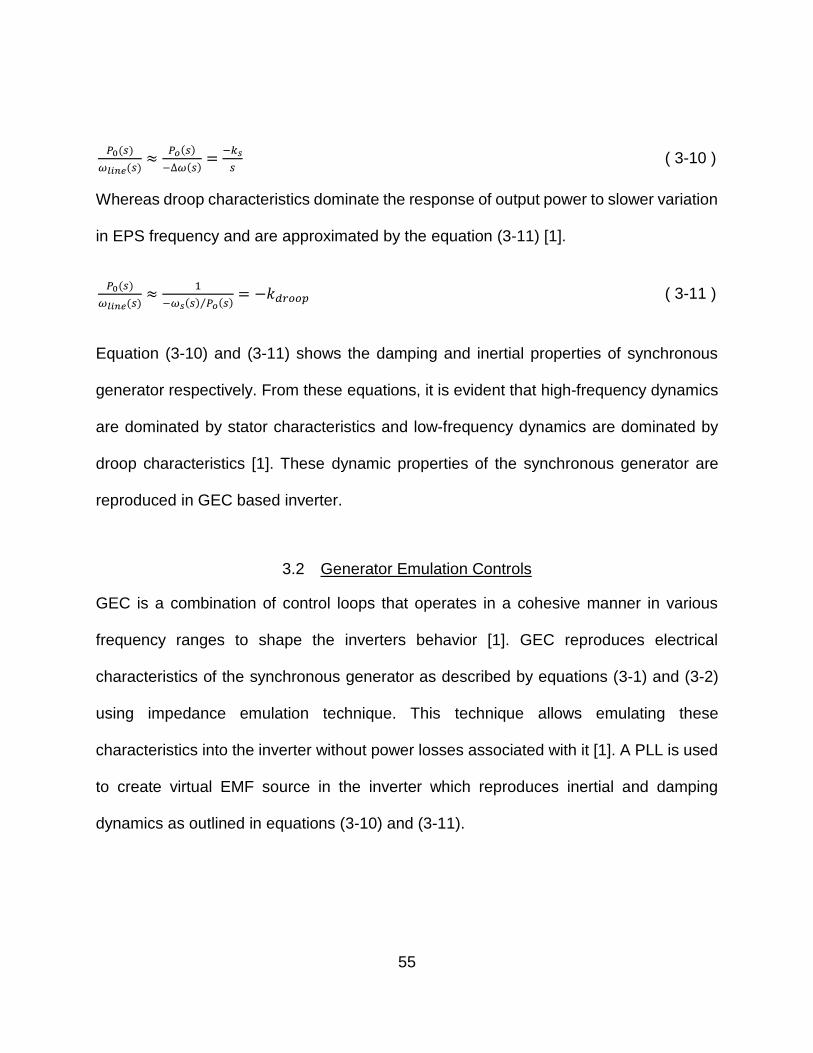
𝑃0(𝑠)
𝜔𝑙𝑖𝑛𝑒(𝑠)≈
𝑃𝑜(𝑠)
−∆𝜔(𝑠)=
−𝑘𝑠
𝑠 ( 3-10 )
Whereas droop characteristics dominate the response of output power to slower variation
in EPS frequency and are approximated by the equation (3-11) [1].
𝑃0(𝑠)
𝜔𝑙𝑖𝑛𝑒(𝑠)≈
1
−𝜔𝑠(𝑠) 𝑃𝑜(𝑠)⁄= −𝑘𝑑𝑟𝑜𝑜𝑝 ( 3-11 )
Equation (3-10) and (3-11) shows the damping and inertial properties of synchronous
generator respectively. From these equations, it is evident that high-frequency dynamics
are dominated by stator characteristics and low-frequency dynamics are dominated by
droop characteristics [1]. These dynamic properties of the synchronous generator are
reproduced in GEC based inverter.
3.2 Generator Emulation Controls
GEC is a combination of control loops that operates in a cohesive manner in various
frequency ranges to shape the inverters behavior [1]. GEC reproduces electrical
characteristics of the synchronous generator as described by equations (3-1) and (3-2)
using impedance emulation technique. This technique allows emulating these
characteristics into the inverter without power losses associated with it [1]. A PLL is used
to create virtual EMF source in the inverter which reproduces inertial and damping
dynamics as outlined in equations (3-10) and (3-11).
56
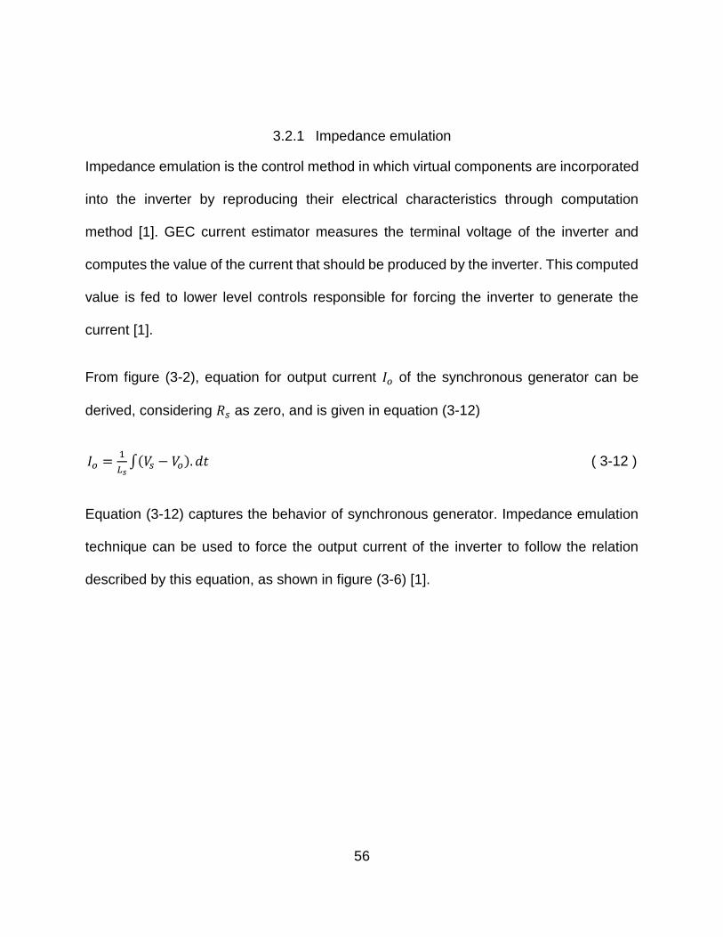
3.2.1 Impedance emulation
Impedance emulation is the control method in which virtual components are incorporated
into the inverter by reproducing their electrical characteristics through computation
method [1]. GEC current estimator measures the terminal voltage of the inverter and
computes the value of the current that should be produced by the inverter. This computed
value is fed to lower level controls responsible for forcing the inverter to generate the
current [1].
From figure (3-2), equation for output current 𝐼𝑜 of the synchronous generator can be
derived, considering 𝑅𝑠 as zero, and is given in equation (3-12)
𝐼𝑜 =1
𝐿𝑠∫(𝑉𝑠 − 𝑉𝑜). 𝑑𝑡 ( 3-12 )
Equation (3-12) captures the behavior of synchronous generator. Impedance emulation
technique can be used to force the output current of the inverter to follow the relation
described by this equation, as shown in figure (3-6) [1].
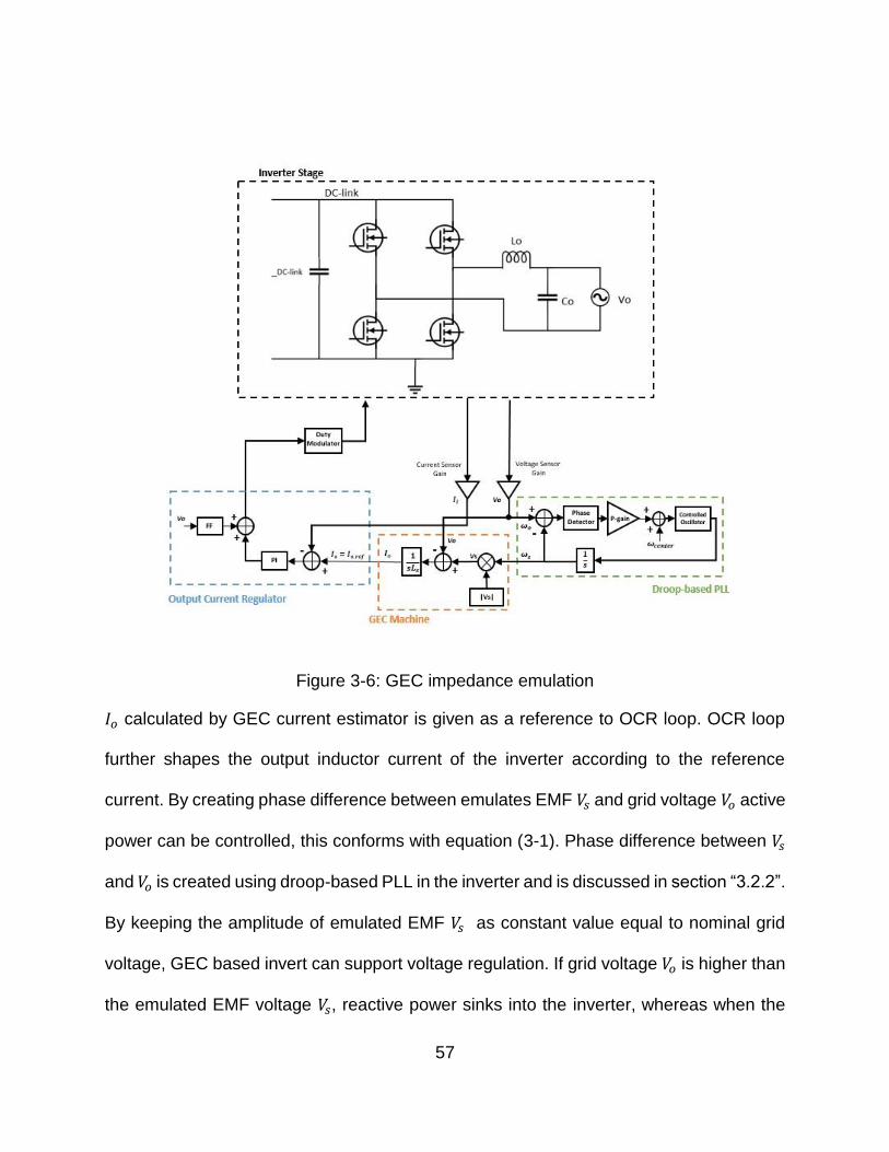
57
Figure 3-6: GEC impedance emulation
𝐼𝑜 calculated by GEC current estimator is given as a reference to OCR loop. OCR loop
further shapes the output inductor current of the inverter according to the reference
current. By creating phase difference between emulates EMF 𝑉𝑠 and grid voltage 𝑉𝑜 active
power can be controlled, this conforms with equation (3-1). Phase difference between 𝑉𝑠
and 𝑉𝑜 is created using droop-based PLL in the inverter and is discussed in section “3.2.2”.
By keeping the amplitude of emulated EMF 𝑉𝑠 as constant value equal to nominal grid
voltage, GEC based invert can support voltage regulation. If grid voltage 𝑉𝑜 is higher than
the emulated EMF voltage 𝑉𝑠, reactive power sinks into the inverter, whereas when the
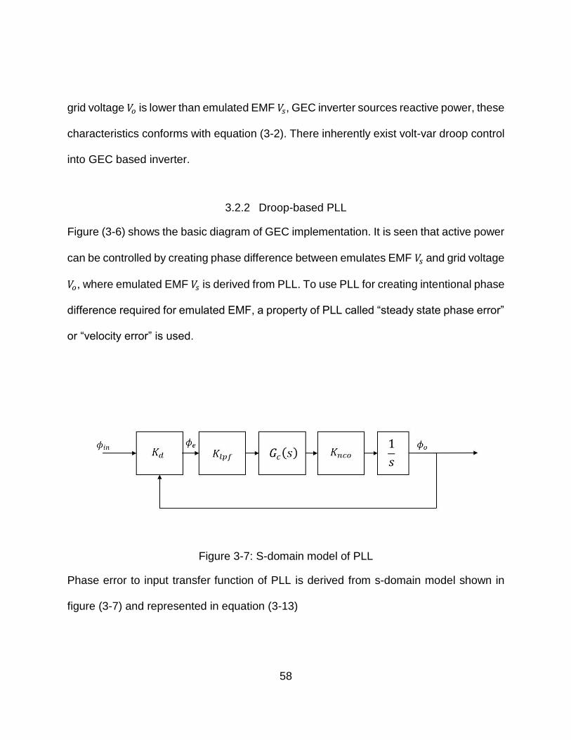
58
grid voltage 𝑉𝑜 is lower than emulated EMF 𝑉𝑠, GEC inverter sources reactive power, these
characteristics conforms with equation (3-2). There inherently exist volt-var droop control
into GEC based inverter.
3.2.2 Droop-based PLL
Figure (3-6) shows the basic diagram of GEC implementation. It is seen that active power
can be controlled by creating phase difference between emulates EMF 𝑉𝑠 and grid voltage
𝑉𝑜, where emulated EMF 𝑉𝑠 is derived from PLL. To use PLL for creating intentional phase
difference required for emulated EMF, a property of PLL called “steady state phase error”
or “velocity error” is used.
Figure 3-7: S-domain model of PLL
Phase error to input transfer function of PLL is derived from s-domain model shown in
figure (3-7) and represented in equation (3-13)

59
𝜙𝑒 =𝜙𝑖𝑛
1+𝐺(𝑠).𝐻(𝑠)=
𝑠
𝑠+𝐾𝑑𝐾𝑙𝑝𝑓𝐺𝑐(𝑠) 𝐾𝑛𝑐𝑜 . 𝜙𝑖𝑛 ( 3-13 )
Final value theorem is applied to the phase error to input transfer function of PLL, to
realize the state of the error after the transient stage. During the transient stage, the input
signal of PLL does a phase change or frequency jump. The error signal generated by PLL
during this stage oscillates due to the large difference between NCO signal and incoming
signal phase before reaching steady state [17]. PLL compensator is used to damp this
oscillation and reduce the phase error.
To see the steady state behavior of PLL for a step change in the input signal frequency,
input signal represented by equation (3-14) is applied to transfer function given in
equation (3-13), and final value theorem is used.
𝜙𝑖𝑛(𝑡) = (𝜔𝑐 − 𝜔𝑜)𝑡 = ∆𝜔𝑡 ( 3-14 )
Where, ∆𝜔 is the difference between input signal frequency 𝜔𝑜 and NCO center frequency
𝜔𝑐. Since PLL is capable of detecting only the phase, step change in frequency is
represented as phase ramp and is given by equation (3-15)
𝜙𝑖𝑛(𝑠) = ∆𝜔
𝑠2 ( 3-15 )
Equation (3-16) shows the final value theorem applied to the phase error to input transfer
function of PLL with phase ramp as an input.

60
lim𝑡→∞
𝜙𝑒(𝑡) = lim𝑠→0
𝑠 𝜙𝑒(𝑠) = lim𝑠→0
𝑠
𝑠+𝐾𝑑𝐾𝑙𝑝𝑓𝐺𝑐(𝑠) 𝐾𝑛𝑐𝑜.
∆𝜔
𝑠2 ( 3-16 )
Equation (3-16) reveals that there exists steady state error for step change in frequency
and is the function of 𝐾𝑑, 𝐾𝑙𝑝𝑓, 𝐺𝑐(𝑠) and 𝐾𝑛𝑐𝑜 given by equation (3-17)
𝜙𝑒 =∆𝜔
𝐾𝑑𝐾𝑙𝑝𝑓𝐺𝑐(𝑠) 𝐾𝑛𝑐𝑜 ( 3-17 )
To remove this steady state phase error, compensator 𝐺𝑐(𝑠) with integral gain is required,
as described in section “2.2.2”. To use PLL for emulated EMF, 𝐺𝑐 is chosen as finite
proportional gain (P) without an integral term. This results into residual phase shift
proportional to the frequency deviation from center frequency [1]. This type of PLL is
called as droop-based PLL. Value of phase error then depends on 𝐾𝑑, 𝐾𝑙𝑝𝑓, 𝑃 and 𝐾𝑛𝑐𝑜
and is shown in equation (3-18)
𝜙𝑒 =∆𝜔
𝐾𝑑𝐾𝑙𝑝𝑓P 𝐾𝑛𝑐𝑜 ( 3-18 )
Figure 3-8 Dynamic model of PLL
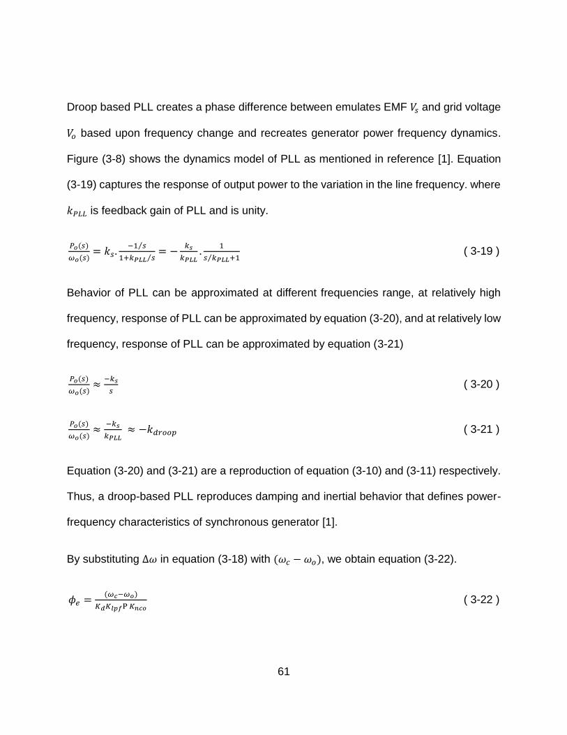
61
Droop based PLL creates a phase difference between emulates EMF 𝑉𝑠 and grid voltage
𝑉𝑜 based upon frequency change and recreates generator power frequency dynamics.
Figure (3-8) shows the dynamics model of PLL as mentioned in reference [1]. Equation
(3-19) captures the response of output power to the variation in the line frequency. where
𝑘𝑃𝐿𝐿 is feedback gain of PLL and is unity.
𝑃𝑜(𝑠)
𝜔𝑜(𝑠)= 𝑘𝑠.
−1 𝑠⁄
1+𝑘𝑃𝐿𝐿 𝑠⁄= −
𝑘𝑠
𝑘𝑃𝐿𝐿.
1
𝑠 𝑘𝑃𝐿𝐿⁄ +1 ( 3-19 )
Behavior of PLL can be approximated at different frequencies range, at relatively high
frequency, response of PLL can be approximated by equation (3-20), and at relatively low
frequency, response of PLL can be approximated by equation (3-21)
𝑃𝑜(𝑠)
𝜔𝑜(𝑠)≈
−𝑘𝑠
𝑠 ( 3-20 )
𝑃𝑜(𝑠)
𝜔𝑜(𝑠)≈
−𝑘𝑠
𝑘𝑃𝐿𝐿 ≈ −𝑘𝑑𝑟𝑜𝑜𝑝 ( 3-21 )
Equation (3-20) and (3-21) are a reproduction of equation (3-10) and (3-11) respectively.
Thus, a droop-based PLL reproduces damping and inertial behavior that defines power-
frequency characteristics of synchronous generator [1].
By substituting ∆𝜔 in equation (3-18) with (𝜔𝑐 − 𝜔𝑜), we obtain equation (3-22).
𝜙𝑒 =(𝜔𝑐−𝜔𝑜)
𝐾𝑑𝐾𝑙𝑝𝑓P 𝐾𝑛𝑐𝑜 ( 3-22 )
62
From equation (3-22) it is observed that center frequency (𝜔𝑐) of PLL can influence
steady state phase difference and therefore the output power. Center frequency can be
used to prioritize the resource utilization. By increasing center frequency higher than
nominal (60 Hz), DG inverter can be engaged to source power at higher grid frequency
(>60 Hz), whereas by reducing center frequency lower than nominal, DG inverter can be
engaged to source power at lower grid frequency (<60 Hz).
3.3 GEC Implementation and Design Consideration
GEC require specific values of the electrical components to be incorporated into current
estimator. The prime parameter of current estimator is stator inductor, 𝐿𝑠. Practical
implementation of the GEC into the inverter requires an integration of additional electrical
components into the current estimator. These additional components consist of DC
resistance and capacitance which reduces DC current build up in current estimator and
damping resistance and capacitance which improves inverter response to harmonic
distortion in load current. Figure (3-9) shows the modified characteristic of emulated
impedance network. In this research, for simplicity, current estimator is implemented
using stator inductor, 𝐿𝑠 and dc-resistance 𝑅𝑑𝑐.
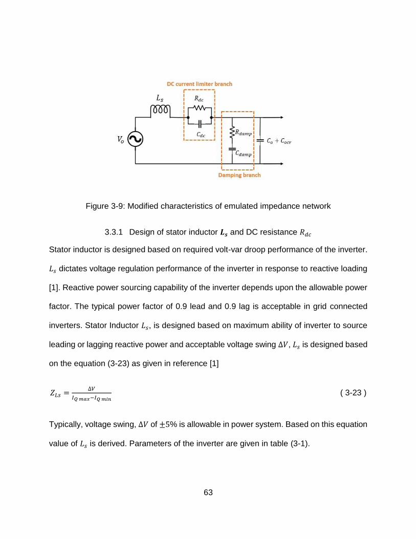
63
Figure 3-9: Modified characteristics of emulated impedance network
3.3.1 Design of stator inductor 𝑳𝒔 and DC resistance 𝑅𝑑𝑐
Stator inductor is designed based on required volt-var droop performance of the inverter.
𝐿𝑠 dictates voltage regulation performance of the inverter in response to reactive loading
[1]. Reactive power sourcing capability of the inverter depends upon the allowable power
factor. The typical power factor of 0.9 lead and 0.9 lag is acceptable in grid connected
inverters. Stator Inductor 𝐿𝑠, is designed based on maximum ability of inverter to source
leading or lagging reactive power and acceptable voltage swing ∆𝑉, 𝐿𝑠 is designed based
on the equation (3-23) as given in reference [1]
𝑍𝐿𝑠 =∆𝑉
𝐼𝑄 𝑚𝑎𝑥−𝐼𝑄 𝑚𝑖𝑛 ( 3-23 )
Typically, voltage swing, ∆𝑉 of ±5% is allowable in power system. Based on this equation
value of 𝐿𝑠 is derived. Parameters of the inverter are given in table (3-1).

64
Table 3-1: Inverter parameters to design stator inductor 𝐿𝑠
Parameters Values
Inverter power (𝑃) 200 𝑊
Invert output voltage or grid voltage (𝑉𝑜) 120 𝑉𝑟𝑚𝑠
Inverter output current (𝐼𝑜) 1.66 𝐼𝑟𝑚𝑠
Allowable power factor (𝑃𝐹) 0.9 lead and 0.9 lag
Allowable voltage swing (𝑉) 12 𝑉
Nominal output frequency (𝑓) 60 𝐻𝑧
Apparent power (S):
𝑆 =𝑃
𝑃𝐹= 222.22 𝑉𝐴
Reactive power (Q):
𝑄 = √|𝑆|2 − |𝑃|2 = ±96.85 𝑉𝑎𝑟
Reactive current (𝐼𝑞):

65
𝐼𝑄 𝑚𝑎𝑥 = +𝑄
𝑉= 0.807 𝐴 𝐼𝑄 𝑚𝑖𝑛 =
−𝑄
𝑉= −0.807 𝐴
Substituting above values in equation (3-23)
𝑍𝐿𝑠 = 2. 𝜋. 𝑓. 𝐿𝑠 =12
0.807 − (−0.807)= 7.434
For nominal frequency 𝑓 is 60Hz, value of 𝐿𝑠 is be obtained and is given in equation
(3-24)
𝐿𝑠 = 19.72 𝑚𝐻 ≈ 20 𝑚𝐻 ( 3-24 )
DC current builds up due to computational artifacts in the GEC system [1]. 𝑅𝑑𝑐 DC
resistance is used to limit the DC current build up since they are undesirable in power
system. 𝑅𝑑𝑐 𝑖𝑠 placed in series with stator inductance 𝐿𝑠 and usually is in vicinity of 5e-3
ohms [1].
𝑅𝑑𝑐 = 7.8133 𝑚𝑂ℎ𝑚 ( 3-25 )
3.3.2 Design of Proportional Gain for Droop-Based PLL
The design of proportional gain for droop-based PLL is based on desired P-𝜔 droop
characteristics of the inverter. IEEE 1547 provides standards for DGs interconnection with
the electric power system. According to IEEE 1547, for DG less than 30kW, frequency
trip thresholds are 59.3Hz for under frequency and 60.5Hz for over frequency [18]. In

66
order to comply with these standards, P-𝜔 droop characteristics should be designed to
operate within this range.
As mentioned in section “3.2.2” center frequency can be used to prioritize resource
utilization. Center frequency can be chosen differently for different energy resources to
engage droop control at different frequencies. Due to powerful economic incentives, DG
inverters with PV are expected to operate at their maximum power all the time [10], and
their center frequency can be programmed such that they source full power near nominal
frequency. Whereas DGs with batteries are usually used to provide short-term energy
requirements to provide stability and expected to source maximum power at the
frequency lower than nominal frequency. This makes them act like ancillary services for
microgrid, particularly for frequency regulation.
Figure (3-10) shows the two different P-𝜔 droop characteristics for DG inverter with PV
and DG inverter with battery. Both the inverters are 200 W inverters. DG inverter with PV
has its center frequency programmed at 60.25 Hz which is much below the over frequency
trip limit, and has a P-𝜔 droop slope of 0.8kW/Hz this results into maximum power at
60Hz. Whereas DG Inverter with battery is programmed with the center frequency at
59.95 Hz with a P-𝜔 droop slope of 0.8kW/Hz. This causes a battery based DG inverter
to source maximum power at 59.70 Hz which is much above - under frequency trip limit.
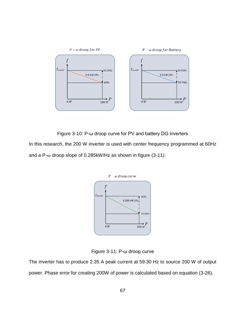
67
Figure 3-10: P-ω droop curve for PV and battery DG inverters
In this research, the 200 W inverter is used with center frequency programmed at 60Hz
and a P-𝜔 droop slope of 0.285kW/Hz as shown in figure (3-11).
Figure 3-11: P-ω droop curve
The inverter has to produce 2.35 A peak current at 59.30 Hz to source 200 W of output
power. Phase error for creating 200W of power is calculated based on equation (3-26).

68
𝐼𝑙_𝑝𝑘 =𝑉𝑠_𝑝𝑘∠𝜙𝑒°−𝑉𝑜_𝑝𝑘∠0°
2𝜋(𝑓)(𝐿)=
120√2∠𝜙𝑒°−120√2∠0°
2𝜋(59.30)(0.02) ( 3-26 )
Equation (3-26) is plotted in figure (3-12), and phase error required to produce 2.35 A
(200 W) power is shown.
Figure 3-12: Peak output current vs Phase error
By creating phase error of 5.924° or 0.1034 radians, 200 W power is sourced at 59.30
Hz. The phase error is listed in the table (3-2) along with the other PLL parameters.
Table 3-2: Parameters to calculate droop PLL gain
Parameters Gain values
𝐾𝑑 0.5
𝐾𝑙𝑝𝑓 1
𝐾𝑛𝑐𝑜 5000
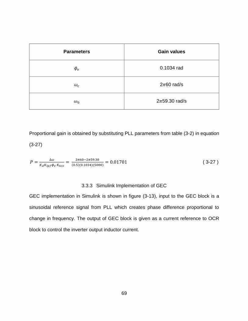
69
Parameters Gain values
𝜙𝑒 0.1034 rad
𝜔𝑐 2𝜋60 rad/s
𝜔0 2𝜋59.30 rad/s
Proportional gain is obtained by substituting PLL parameters from table (3-2) in equation
(3-27)
𝑃 =∆𝜔
𝐾𝑑𝐾𝑙𝑝𝑓𝜙𝑒 𝐾𝑛𝑐𝑜=
2𝜋60−2𝜋59.30
(0.5)(0.1034)(5000)= 0.01701 ( 3-27 )
3.3.3 Simulink Implementation of GEC
GEC implementation in Simulink is shown in figure (3-13), input to the GEC block is a
sinusoidal reference signal from PLL which creates phase difference proportional to
change in frequency. The output of GEC block is given as a current reference to OCR
block to control the inverter output inductor current.

70
Figure 3-13: GEC Implementation in Simulink
Inside the GEC block equation (3-12) is implemented. Integral is implemented using
backward Euler approximation. Equation (3-28) shows the scaling of 𝐿𝑠.
1
𝑠.𝐿𝑠⟶
𝑇𝑠
𝐿𝑠.
𝑧
𝑧−1 ( 3-28)
Where, 𝑇𝑠 is sampling time and is 50usec and ‘z’ is the delay block with delay of 50e-6
sec. Implementation of GEC block is shown in figure (3-14).
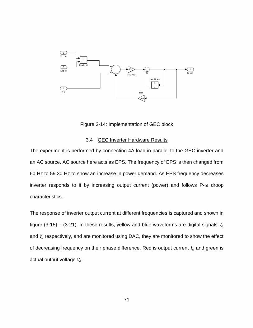
71
Figure 3-14: Implementation of GEC block
3.4 GEC Inverter Hardware Results
The experiment is performed by connecting 4A load in parallel to the GEC inverter and
an AC source. AC source here acts as EPS. The frequency of EPS is then changed from
60 Hz to 59.30 Hz to show an increase in power demand. As EPS frequency decreases
inverter responds to it by increasing output current (power) and follows P-𝜔 droop
characteristics.
The response of inverter output current at different frequencies is captured and shown in
figure (3-15) – (3-21). In these results, yellow and blue waveforms are digital signals 𝑉𝑜
and 𝑉𝑠 respectively, and are monitored using DAC, they are monitored to show the effect
of decreasing frequency on their phase difference. Red is output current 𝐼𝑜 and green is
actual output voltage 𝑉𝑜.
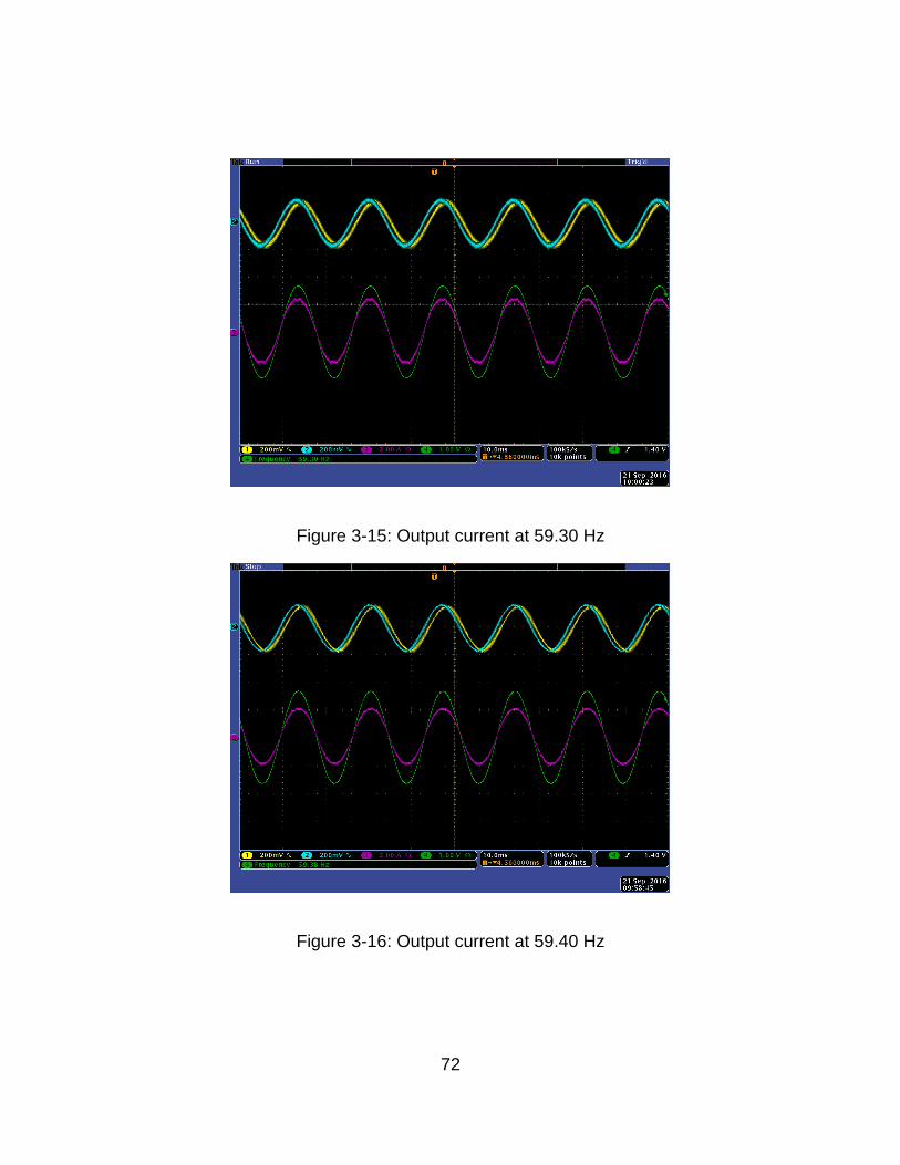
72
Figure 3-15: Output current at 59.30 Hz
Figure 3-16: Output current at 59.40 Hz
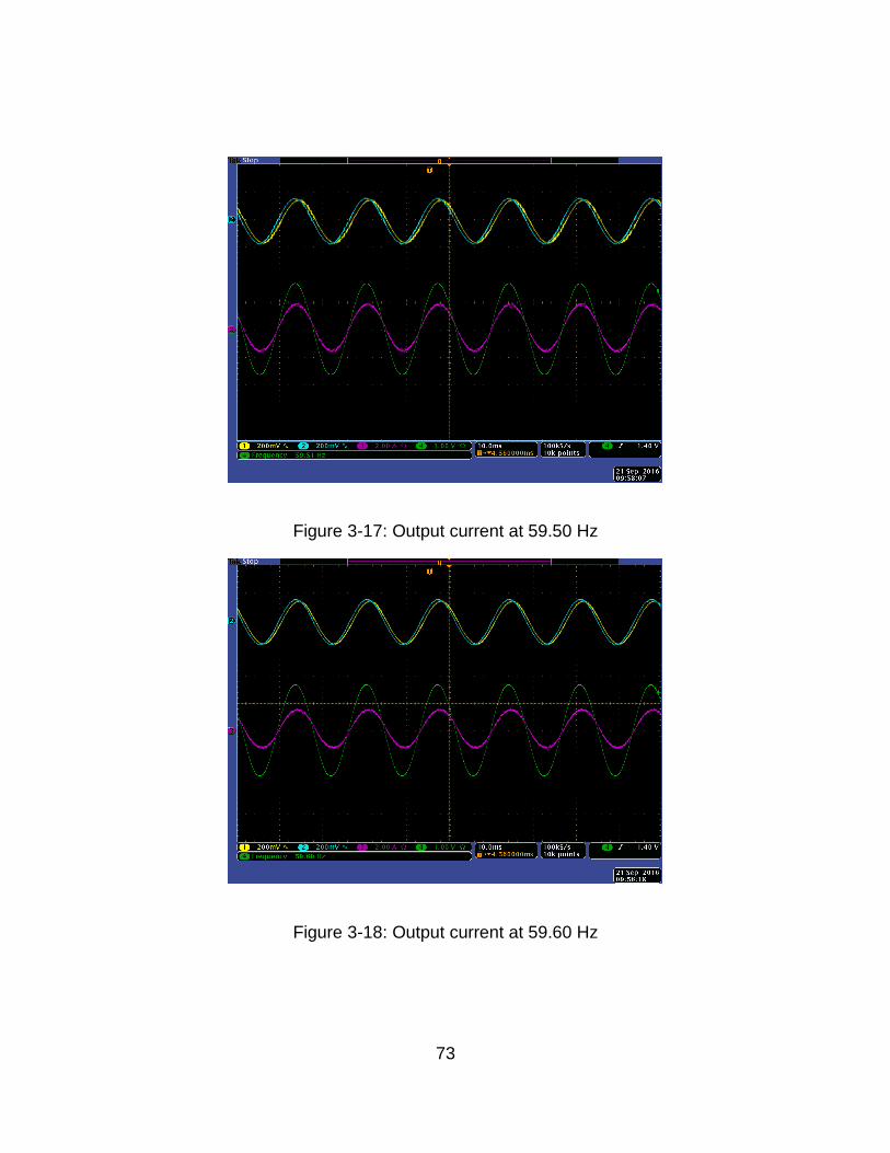
73
Figure 3-17: Output current at 59.50 Hz
Figure 3-18: Output current at 59.60 Hz

74
Figure 3-19: Output current at 59.70 Hz
Figure 3-20: Output current at 59.80 Hz

75
Figure 3-21: Output current at 59.90 Hz

76
CHAPTER 4: VIRTUAL RESISTANCE BASED DC-LINK VOLTAGE REGULATION FOR GEC INVERTERS
DC-link voltage regulation is used to carry out average power balance between inverter
output power and available input power from the energy source. It regulates the DC-link
voltage of the inverter slightly above the peak voltage of the grid, which inherently leads
to average power balance.
For the grid-forming inverters used in a microgrid, DC-link voltage regulator limits the
demanded power by shaping its P-𝜔 droop characteristics based on available input power
from the microsource. DC-link voltage regulator is crucial for operating grid-forming
inverter and its control dynamics and implementation are discussed in this chapter.
4.1 DC-link voltage regulator for Grid-following Inverter
Figure (4-1) shows the single stage grid-following inverter with the DC-link voltage
regulator. 𝐼𝑟𝑒𝑓 dictating the output current of the inverter and hence the output power. If
𝐼𝑟𝑒𝑓 is set to source power higher than the power available from the microsource, DC-link
voltage of the grid decreases. If the DC-link voltage falls below peak-grid voltage, the
current from the grid rushes into the inverter via switching bridge body diode and inverter
becomes uncontrollable. Normally lower limit is placed on DC-link voltage to disconnect
inverter in this situation.
Average power balance between the output power and available input power is
maintained by DC-link voltage regulator loop by controlling 𝐼𝑟𝑒𝑓. DC-link voltage regulator
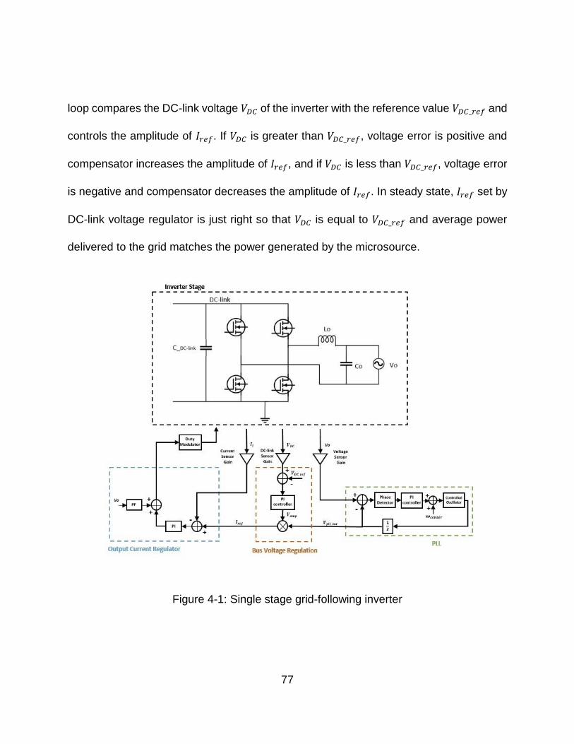
77
loop compares the DC-link voltage 𝑉𝐷𝐶 of the inverter with the reference value 𝑉𝐷𝐶_𝑟𝑒𝑓 and
controls the amplitude of 𝐼𝑟𝑒𝑓. If 𝑉𝐷𝐶 is greater than 𝑉𝐷𝐶_𝑟𝑒𝑓, voltage error is positive and
compensator increases the amplitude of 𝐼𝑟𝑒𝑓, and if 𝑉𝐷𝐶 is less than 𝑉𝐷𝐶_𝑟𝑒𝑓, voltage error
is negative and compensator decreases the amplitude of 𝐼𝑟𝑒𝑓. In steady state, 𝐼𝑟𝑒𝑓 set by
DC-link voltage regulator is just right so that 𝑉𝐷𝐶 is equal to 𝑉𝐷𝐶_𝑟𝑒𝑓 and average power
delivered to the grid matches the power generated by the microsource.
Figure 4-1: Single stage grid-following inverter
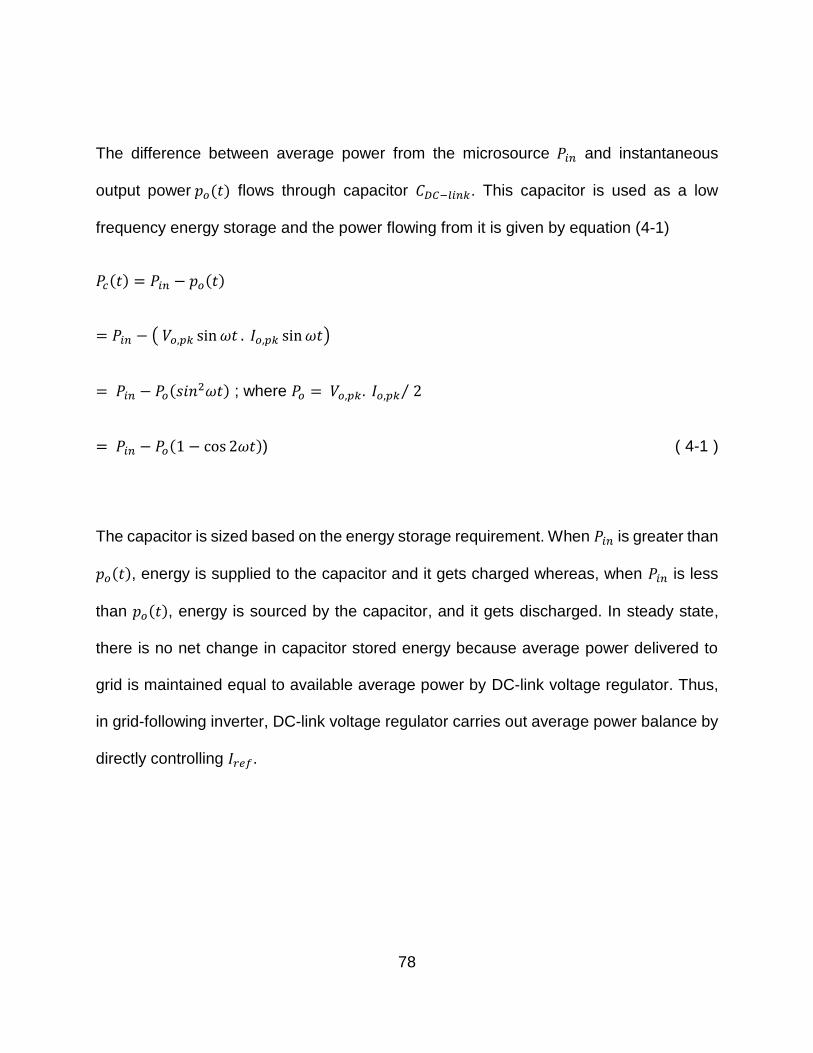
78
The difference between average power from the microsource 𝑃𝑖𝑛 and instantaneous
output power 𝑝𝑜(𝑡) flows through capacitor 𝐶𝐷𝐶−𝑙𝑖𝑛𝑘. This capacitor is used as a low
frequency energy storage and the power flowing from it is given by equation (4-1)
𝑃𝑐(𝑡) = 𝑃𝑖𝑛 − 𝑝𝑜(𝑡)
= 𝑃𝑖𝑛 − ( 𝑉𝑜,𝑝𝑘 sin 𝜔𝑡 . 𝐼𝑜,𝑝𝑘 sin 𝜔𝑡)
= 𝑃𝑖𝑛 − 𝑃𝑜(𝑠𝑖𝑛2𝜔𝑡) ; where 𝑃𝑜 = 𝑉𝑜,𝑝𝑘. 𝐼𝑜,𝑝𝑘 2⁄
= 𝑃𝑖𝑛 − 𝑃𝑜(1 − cos 2𝜔𝑡)) ( 4-1 )
The capacitor is sized based on the energy storage requirement. When 𝑃𝑖𝑛 is greater than
𝑝𝑜(𝑡), energy is supplied to the capacitor and it gets charged whereas, when 𝑃𝑖𝑛 is less
than 𝑝𝑜(𝑡), energy is sourced by the capacitor, and it gets discharged. In steady state,
there is no net change in capacitor stored energy because average power delivered to
grid is maintained equal to available average power by DC-link voltage regulator. Thus,
in grid-following inverter, DC-link voltage regulator carries out average power balance by
directly controlling 𝐼𝑟𝑒𝑓.

79
4.2 DC-link voltage regulator for GEC grid-forming Inverter using virtual resistance technique
In GEC grid-forming inverters, the output power of the inverter is based on the P-𝜔 droop
characteristics of the inverter. Figure (4-2) shows the GEC grid-forming inverters operated
in islanded mode.
In islanded microgrid, GEC inverter operating voltage and frequency are determined by
the total load and the sources connected in the EPS. To source demanded power by the
load, the GEC inverter creates a proportional phase difference between emulated EMF
𝑉𝑠 and output voltage 𝑉𝑜 by drooping or reducing output voltage frequency 𝜔0 below its
center frequency 𝜔𝑐𝑒𝑛𝑡𝑒𝑟. This allows the sharing of the load among the GEC inverters
connected in the microgrid. Thus with increase in the load power, GEC inverters droops
their output voltage frequency 𝜔0, and sources power depending upon their P-𝜔 droop
characteristics.

80
Figure 4-2: Grid-forming Inverters operated in islanded mode.
In this configuration, a situation may arise when the inverter cannot further source power
to the load due to its operating limitation such as in-availability of sufficient power from
the microsource or limited rating of the inverter [1]. If the inverters are still allowed to follow
their P-𝜔 droop curve and source power to the load, the DC-link voltage of these inverters
will drop below its nominal value, resulting in under voltage limit fault and disconnecting
them form the microgrid network. This behavior may abruptly increase power demand on
the rest of the sources connected in the microgrid and overload them until corrective
actions are taken by the higher level control of the microgrid. This may lead to cascades
failure and can have a catastrophic impact on the viability of the entire system [8]
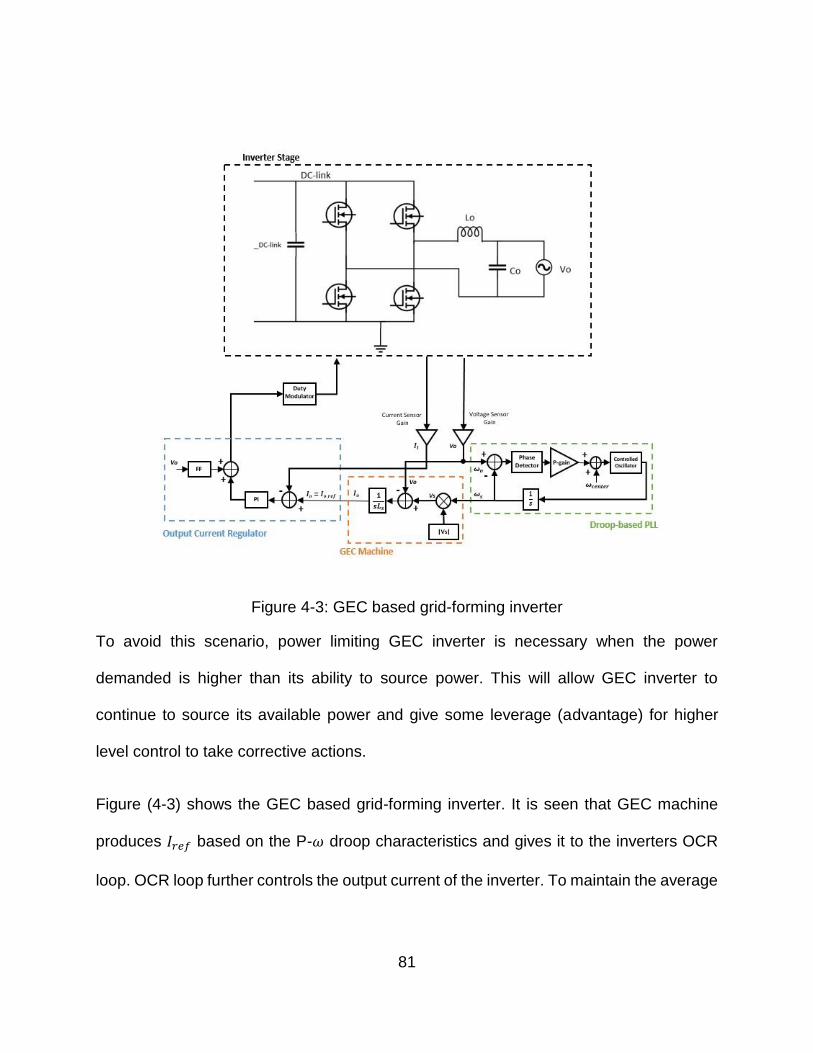
81
Figure 4-3: GEC based grid-forming inverter
To avoid this scenario, power limiting GEC inverter is necessary when the power
demanded is higher than its ability to source power. This will allow GEC inverter to
continue to source its available power and give some leverage (advantage) for higher
level control to take corrective actions.
Figure (4-3) shows the GEC based grid-forming inverter. It is seen that GEC machine
produces 𝐼𝑟𝑒𝑓 based on the P-𝜔 droop characteristics and gives it to the inverters OCR
loop. OCR loop further controls the output current of the inverter. To maintain the average

82
power balance, a mechanism is required to control 𝐼𝑟𝑒𝑓 when power demanded by the P-
𝜔 droop is higher than the available power.
Figure 4-4: Virtual resistance integrated emulated impedance network
𝐼𝑟𝑒𝑓 is controlled in GEC inverter by incorporating virtual resistance component into the
emulated impedance network as shown in figure (4-4). Virtual resistance acts as a control
handle for the DC-link voltage regulator loop. Output current of the current estimator 𝐼𝑜
which sets the current reference 𝐼𝑟𝑒𝑓 is reduced by the current flowing into the virtual
resistance 𝐼𝑅𝑣 as given by equation (4-2)
𝐼𝑟𝑒𝑓 = 𝐼𝑜 − 𝐼𝑅𝑣 ( 4-2 )
The conductivity (𝑔) of the virtual resistance is controlled to control the 𝐼𝑟𝑒𝑓 when the
inverter is commanded to operate beyond its power capability. Sensed DC-link voltage
𝑉𝐷𝐶 is compared with the DC link reference voltage 𝑉𝐷𝐶_𝑟𝑒𝑓 and the error signal 𝑉𝑒𝑟𝑟𝑜𝑟 is
83
generated. If the DC link voltage falls below the DC link reference voltage, the voltage
error becomes positive and the compensator 𝐺𝑐 increases the conductivity of the virtual
resistance. This increases 𝐼𝑅𝑣 and in turn decreases 𝐼𝑟𝑒𝑓, from equation (4-2). This
mechanism limits the output current of the GEC inverter and restores the DC link voltage
to the reference value. Thus, the virtual resistance based DC-link voltage regulator
shapes the P- ω droop curve and does not allow the inverter to operate beyond its power
capability. If the DC-link voltage is higher than the DC-link voltage reference, the error
voltage becomes negative and limiter logic disables the virtual resistance based DC-link
voltage regulator, and P-𝜔 droop control of the inverter controls the output power.
4.3 Modeling and Control Design for DC-link voltage regulator
Dynamics of DC-link voltage are governed by power flowing in the DC-link capacitor given
by equation (4-1). Therefore, DC-link voltage is composed of slow varying signals and
harmonic component 2𝜔. To derive DC-link voltage, current in the DC-link capacitor is
required and is given by equation (4-3)
𝑖𝐶𝐷𝐶−𝑙𝑖𝑛𝑘 (𝑡) =𝑃𝑖𝑛−𝑝𝑜(𝑡)
𝑣𝐷𝐶−𝑙𝑖𝑛𝑘(𝑡) ( 4-3 )
Ripples in the DC-link voltage are much smaller than the average DC-link voltage since
ripples are usually tens of volts and DC-link voltage is typically hundreds of volts [19].
𝑣𝐷𝐶−𝑙𝑖𝑛𝑘(𝑡) = 𝑉𝐷𝐶−𝑙𝑖𝑛𝑘,𝑎𝑣𝑔 + 𝑟𝑖𝑝𝑝𝑙𝑒(𝑡)
84
Considering, 𝑟𝑖𝑝𝑝𝑙𝑒(𝑡) < < 𝑉𝐷𝐶−𝑙𝑖𝑛𝑘,𝑎𝑣𝑔
Thus, DC-link voltage can be considered as averaged DC-link voltage and is given by
equation (4-4)
𝑣𝐷𝐶−𝑙𝑖𝑛𝑘(𝑡) ≈ 𝑉𝐷𝐶−𝑙𝑖𝑛𝑘,𝑎𝑣𝑔 ( 4-4 )
Substituting equation (4-4) in equation (4-3), to derives current in the DC-link capacitor.
𝑖𝐶𝐷𝐶−𝑙𝑖𝑛𝑘 (𝑡) =𝑃𝑖𝑛−𝑝𝑜(𝑡)
𝑉𝐷𝐶−𝑙𝑖𝑛𝑘,𝑎𝑣𝑔 ( 4-5 )
Dynamic Voltage across DC-link is obtained by integrating the DC-link capacitor current
as shown in equation (4-6)
𝑣𝐷𝐶−𝑙𝑖𝑛𝑘(𝑡) =1
𝐶𝐷𝐶−𝑙𝑖𝑛𝑘∫
𝑃𝑖𝑛−𝑝𝑜(𝑡)
𝑉𝐷𝐶−𝑙𝑖𝑛𝑘,𝑎𝑣𝑔 𝑑𝑡 ( 4-6 )
This model leads to dynamic DC-link voltage which is not linear and not time-invariant
because of output power 𝑝𝑜(𝑡) is instantaneous power.
To develop DC-link voltage regulator controller, a linear and time invariant model is
required. To make dynamic model linear and time invariant, average output power needs
to be considered, 𝑝𝑜(𝑡) ⇒ 𝑃𝑜,𝑎𝑣𝑔. Substituting equation 𝑃𝑜,𝑎𝑣𝑔 in equation (4-6), we obtain
dynamic equation for DC-link voltage which is linear and time invariant and is given by
equation (4-7).
85
𝑣𝐷𝐶−𝑙𝑖𝑛𝑘(𝑡) =1
𝐶𝐷𝐶−𝑙𝑖𝑛𝑘.𝑉𝐷𝐶−𝑙𝑖𝑛𝑘,𝑎𝑣𝑔∫ 𝑃𝑖𝑛 − 𝑃𝑜,𝑎𝑣𝑔 . 𝑑𝑡 ( 4-7 )
A dynamic model of DC-link voltage is shown in figure (4-5).
Figure 4-5: Dynamic model of DC-link voltage
In GEC inverters, P-ω droop control gives the demanded power, 𝑃𝑑𝑒𝑚𝑎𝑛𝑑 based on
system frequency, 𝜔𝑜. In case of demanded power higher than the available power, virtual
resistance based DC-link regulation activates as mentioned in section 4.2 and dissipates
part of demanded power, thus reducing it. Referring to Figure (4-4), average power
dissipated by virtual resistance is given by equation (4-8)
𝑃𝑅𝑣=
𝑉𝑜,𝑟𝑚𝑠2
𝑅𝑣= 𝑉𝑜,𝑟𝑚𝑠
2 . 𝑔 ( 4-8 )
Where, 𝑔 is the conductivity of the virtual resistance and 𝑃𝑅𝑣 is the average, virtual power
is dissipated across virtual resistance 𝑅𝑣. Equation (4-9) show the average output power,
𝑃𝑜,𝑎𝑣𝑔 left after reducing virtual power from the demanded power, 𝑃𝑑𝑒𝑚𝑎𝑛𝑑.

86
𝑃𝑜,𝑎𝑣𝑔 = 𝑃𝑑𝑒𝑚𝑎𝑛𝑑 − 𝑃𝑅𝑣 ( 4-9 )
Equation (4-8) and (4-9) forms the model of virtual resistance and is shown in figure
(4-6).
Figure 4-6: Virtual resistance model
A dynamic model of DC-link voltage and the model of virtual resistance are connected in
a closed loop as shown in figure (4-7). Dynamic DC-link voltage 𝑣𝐷𝐶−𝑙𝑖𝑛𝑘(𝑡) is compared
with DC-link a reference voltage 𝑉𝐷𝐶−𝑙𝑖𝑛𝑘 and error is given to compensator 𝐺𝑐.
Compensator 𝐺𝑐 produces the correcting signal 𝑔(𝑡) based upon voltage error, 𝑣𝑒𝑟𝑟𝑜𝑟(𝑡).
Plant 𝐺𝑣𝑔(𝑠) of dynamic model is given by equation (4-10)
𝐺𝑣𝑔(𝑠) =𝑣𝐷𝐶−𝑙𝑖𝑛𝑘(𝑠)
𝑔(𝑠)=
𝑉𝑜,𝑟𝑚𝑠2
𝐶𝐷𝐶−𝑙𝑖𝑛𝑘.𝑉𝐷𝐶−𝑙𝑖𝑛𝑘,𝑎𝑣𝑔.
1
𝑠 ( 4-10 )

87
Figure 4-7: Dynamic model of virtual resistance based DC-link voltage regulator
DC-link compensator 𝐺𝑐 is designed based on loop gain 𝐺𝑣𝑔(𝑠). 𝐻(𝑠), where 𝐻(𝑠) is unity.
System parameters to design virtual resistance based DC-link regulator are listed in Table
(4-1)
Table 4-1: Inverter parameters to designing DC-link voltage regulator loop
Parameters Values
𝑉𝐷𝐶−𝑙𝑖𝑛𝑘,𝑎𝑣𝑔 200 V
𝑉𝑜,𝑟𝑚𝑠 120 V
𝐶𝐷𝐶−𝑙𝑖𝑛𝑘 400 uF
𝑃𝑜 200 W

88
Compensator 𝐺𝑐 is inverter zero type of PI controller as shown in equation (4-11). To
design PI controller, uncompensated loop gain 𝐺𝑣𝑔(𝑠). 𝐻(𝑠) is first plotted as shown in
figure (4-8).
Based on the bode plot values of 𝑘𝑝 and 𝑓𝑧 are chosen to create desired cross over
frequency (𝑓𝑐) and phase margin (Φ𝑚).
𝐺𝑐(𝑠) = 𝑘𝑝 +𝑘𝑖
𝑠= 𝑘𝑝 (1 +
2.𝜋.𝑓𝑧
𝑠) ( 4-11 )
Figure 4-8: Uncompensated DC-link voltage regulator loop gain
The PI controller for the DC-link voltage regulator is designed to maintain DC-link voltage
typically higher than peak AC voltage and lower than rated voltage of DC-link capacitor.
In this case [19], DC-link voltage is regulated at 200V. Typically it is desired that the DC-
89
link voltage regulator loop bandwidth is set high so that it can quickly respond to changes
in DC-link voltage and regulate it. Another constraint in designing DC-link voltage
regulator loop is second order harmonics distortion in output current. According to
IEEE1547 standard, THD is required to be less than 5% at rated power [19]. Therefore,
to design DC-link voltage regulator with high bandwidth, it is imperative to reduce second
order harmonics on DC-link capacitor voltage. Second order harmonics are placed at
120Hz (2𝜔), to reduce these harmonics, digital IIR low pass filter is implemented. This
filter has a cut of frequency of 50 Hz and it reduces the harmonics on sensed DC-link
voltage. The PI controller is designed for crossover frequency of 45 Hz and phase margin
greater than 71°, by choosing 𝑘𝑝 as 0.001479 and 𝑓𝑧 as 15Hz. Figure (4-9) shows the
compensated loop gain 𝐺𝑐(𝑠). 𝐺𝑣𝑔(𝑠). 𝐻(𝑠).

90
Figure 4-9: Compensated DC-link voltage regulator loop-gain
4.4 Implementation of Virtual Resistance based DC-link Voltage Regulator
Implementation of dynamic model of DC-link voltage and regulator are shown in figure
(4-10).

91
Figure 4-10: Dynamic model of DC-link voltage and DC-link voltage regulator
A dynamic model of DC-link voltage is implemented in Simulink. This model is a non-
linear model as output power is instantaneous power. Output power is then subtracted
from the input power to obtain power in the DC-link capacitor. DC-link voltage is then
derived implementing equation (4-6). The integral block is initialized with 200 V value to
avoid divide by zero error. ZOH block samples the DC-link voltage at 5 kHz frequency
and gives it to low pass filter.
Digital IIR Low pass filter is implemented to filter out second harmonic 2𝜔 term on DC-
link voltage. The implementation is same as LPF filter in PLL. Required crossover
frequency (𝑓𝑐) is 50Hz with gain (𝐺) of unity and sampling frequency (𝑓𝑠𝑎𝑚𝑝𝑙𝑒) is 5 kHz.
Digital IIR low pass filter is given by the form shown in equation (4-12).
𝐻(𝑧) =𝑏0
1+(𝑏0−1).𝑧−1 ( 4-12 )
92
Where, 𝑏0 =𝐺
𝜏.𝑓𝑠𝑎𝑚𝑝𝑙𝑒 and 𝜏 =
1
2𝜋.𝑓𝑐
Substituting values into equation (4-12), we get equation (4-13).
𝐻(𝑧) =0.0628
1−(0.9371).𝑧−1 ( 4-13 )
Where, 𝑧−1 is the unit delay of 200e-6 sec. Equation (4-14) is implemented inside LPF
block, in figure (4-10).
The PI controller is designed in section “4.3”, and the implementation is similar to the PI
controller implementation in PLL.
𝑘𝑝 = 0.001479
𝑘𝑖 = 2𝜋𝑓𝑧 . 𝑘𝑝 = 0.1393
These values are in the continuous domain and are digitally implemented by backward
Euler approximation. By substituting 𝑠 ⟶𝑧−1
𝑧.𝑇𝑠 in equation (4-11), digital PI controller is
obtained as shown in equation (4-14).
𝐺𝑐(𝑧) = 𝑘𝑝 + 𝑘𝑖. 𝑇𝑠.𝑧
𝑧−1 ( 4-14 )
𝑘𝑝_𝑑𝑖𝑔𝑖𝑡𝑎𝑙 = 0.001479
𝑘𝑖_𝑑𝑖𝑔𝑖𝑡𝑎𝑙 = 2. 𝜋. 𝑓𝑧 . 𝑘𝑝_𝑑𝑖𝑔𝑖𝑡𝑎𝑙 . 𝑇𝑠 = 0.1393. (1
5𝑘𝐻𝑧) = 0.02786𝑒 − 3

93
Equation (4-14) is implemented inside PI-controller block in figure (4-10). Saturation block
is implemented to make control voltage zero when it goes negative. This block disables
virtual resistance based DC-link voltage regulator when DC-link voltage is higher than
DC-link reference. Virtual resistance embedded in GEC model is shown in figure (4-11).
Figure 4-11: Virtual resistance embedded in GEC model
Virtual resistor’s conductivity, 𝑔 computed by PI controller is given as an input to GEC
model. 𝑔 multiplied by the output voltage gives the current in the virtual resistance 𝐼𝑅𝑣.
This current is then subtracted from actual output current 𝐼𝑜 and the reference current 𝐼𝑟𝑒𝑓
is generated. Figure 4-12. shows the integration of virtual resistance based DC-link
voltage regulator in GEC inverter.

94
Figure 4-12: GEC inverter with virtual resistance based DC-link voltage regulator
4.5 Results of Virtual Resistance based DC-link Regulator
To demonstrate the concept of power limited inverters, GEC programmed inverters were
operated with input power limited to 148 Watts and step changing the power demand
from 57 Watts to 200 Watts. Power demand was emulated by changing the frequency of
AC source from 59.80 Hz corresponds to 57 Watts to 59.30 Hz corresponds to 200 Watt.
Figure (4-13) shows the drop-in DC-link voltage (green) as the current increase higher
than 1.74A. The controller takes action, and Integral output (yellow) increases to
compensate the change in DC-link voltage. Virtual resistance current (𝐼𝑅𝑣) (blue)
increases which in turn decreases output current (pink) as it follows equation (4-2). This
brings DC-link voltage back to 200 V.

95
Figure 4-13: DC-link voltage regulator

96
CHAPTER 5: CONCLUSION
Inverters operated in a microgrid are categorized mainly into grid-forming inverter or grid-
following inverters. This research focuses on grid-forming inverters which can be
operated independently of the grid, i.e. in islanded microgrid. Generator Emulation
Control strategy (GEC) for grid-forming inverters is demonstrated in this research. GEC
inverter emulates dynamic properties of synchronous generator like damping and inertia
which makes grid-forming inverter behave like a synchronous generator.
Correlation between GEC inverter and the synchronous generator is drawn based on the
dynamic equations. Modeling, control design and implementation of all the control blocks
is carried out in this research. Hardware results for GEC are presented in section 3.4,
which confirms the P-𝜔 droop charatersitics of GEC inverter.
The power-limiting nature of the grid-forming inverters is analyzed, and the control
problems associated with it are mentioned. Virtual resistance based DC-link voltage
regulation technique is introduced to maintain the average power balance in grid-forming
inverters. This technique can be easily integrated into GEC model, and DC-link voltage
regulation can be carried out. Modeling, control design and implementation for virtual
resistance based DC-link voltage regulator is carried out in this research.
Results for virtual resistance based DC-link voltage regulator are shown in section 4.5.
These results confirm the regulation of DC-link voltage when power demand is higher
than the power available. In the experiment, the input power of the GEC inverter is limited

97
to 148 Watts. When power demanded by the load is higher than 148 Watts, frequency of
the system droops below 59.48 Hz and P-𝜔 droop charatersitics of GEC inverter dictates
the inverter to source power more than 148 W. Since the inverter cannot source any more
power than 148 W, its DC-link voltage starts to collapse. This event activates virtual
resitance based DC-link voltage regulator and average power balance is maintained by
shaping P-𝜔 droop control as shown in figure (5-1)
Figure 5-1: Power-limited P-𝜔 droop curve of GEC inverter
Thus, P-𝜔 droop charatersitics of GEC inverter are shaped to maintin average power
balance and allow the inverter to source its available power. Virtual resistance based DC-
link voltage regulation carries out power limit management in grid-froming inverters.
98
APPENDIX: EXPERIMENTAL SETUP
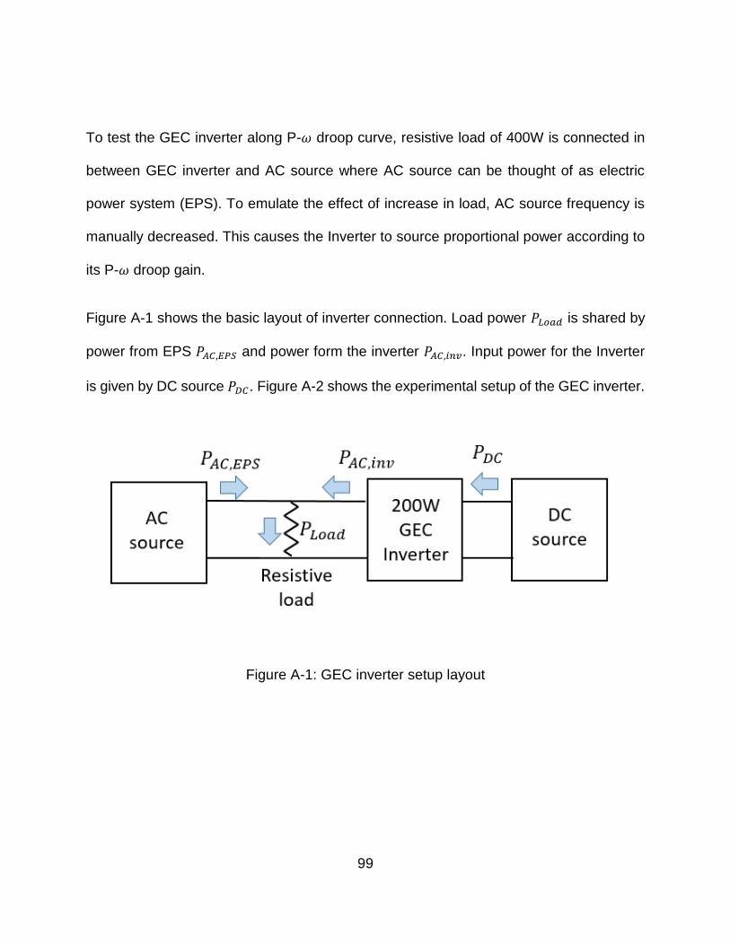
99
To test the GEC inverter along P-𝜔 droop curve, resistive load of 400W is connected in
between GEC inverter and AC source where AC source can be thought of as electric
power system (EPS). To emulate the effect of increase in load, AC source frequency is
manually decreased. This causes the Inverter to source proportional power according to
its P-𝜔 droop gain.
Figure A-1 shows the basic layout of inverter connection. Load power 𝑃𝐿𝑜𝑎𝑑 is shared by
power from EPS 𝑃𝐴𝐶,𝐸𝑃𝑆 and power form the inverter 𝑃𝐴𝐶,𝑖𝑛𝑣. Input power for the Inverter
is given by DC source 𝑃𝐷𝐶. Figure A-2 shows the experimental setup of the GEC inverter.
Figure A-1: GEC inverter setup layout

100
Figure A-2: GEC inverter experimental setup
101
LIST OF REFERENCES
[1] H. Alatrash, A. Mensah, E. Mark, G. Haddad and J. Enslin, "Generator Emulation Controls
for Photovoltaic Inverters," in IEEE Transactions on Smart Grid, vol. 3, no. 2, pp. 996-1011,
June 2012.
[2] Herong Gu, Deyu Wang, Hong Shen, Wei Zhao, and Xiaoqiang Guo, “New Power Sharing
Control for Inverter-Dominated Microgrid Based on Impedance Match Concept,” The
Scientific World Journal, vol. 2013, Article ID 816525, 7 pages, 2013
[3] Hassan Bevrani, Toshifumi Ise, Yushi Miura, Virtual synchronous generators: A survey and
new perspectives, International Journal of Electrical Power & Energy Systems, Volume 54,
January 2014, Pages 244-254, ISSN 0142-0615.
[4] Y. W. Li and C. N. Kao, "An Accurate Power Control Strategy for Power-Electronics-
Interfaced Distributed Generation Units Operating in a Low-Voltage Multibus Microgrid,"
in IEEE Transactions on Power Electronics, vol. 24, no. 12, pp. 2977-2988, Dec. 2009.
[5] Amandeep Kaur, Jitender Kaushal, Prasenjit Basak, A review on microgrid central
controller, Renewable and Sustainable Energy Reviews, Volume 55, March 2016, Pages
338-345, ISSN 1364-0321.
[6] H. Han, X. Hou, J. Yang, J. Wu, M. Su and J. M. Guerrero, "Review of Power Sharing
Control Strategies for Islanding Operation of AC Microgrids," in IEEE Transactions on
Smart Grid, vol. 7, no. 1, pp. 200-215, Jan. 2016.
102
[7] A. Maknouninejad, N. Kutkut, I. Batarseh, Z. Qu and E. Shoubaki, "Detailed analysis of
inverter linear control loops design," Applied Power Electronics Conference and Exposition
(APEC), 2011 Twenty-Sixth Annual IEEE, Fort Worth, TX, 2011, pp. 1188-1193.
[8] M. Wytock, S. Salapaka and M. Salapaka, "Preventing cascading failures in microgrids with
one-sided support vector machines," 53rd IEEE Conference on Decision and Control, Los
Angeles, CA, 2014, pp. 3252-3258.
[9] F. Z. Peng, Y. W. Li and L. M. Tolbert, "Control and protection of power electronics
interfaced distributed generation systems in a customer-driven microgrid," 2009 IEEE
Power & Energy Society General Meeting, Calgary, AB, 2009, pp. 1-8.
[10] M. J. Erickson, “Improved power control of inverter sources in mixed-source microgrid”,
Ph.D. dissertation, Dept. Elect. Eng., University of Wisconsin-Madison, 2013.
[11] A. Bidram and A. Davoudi, "Hierarchical Structure of Microgrids Control System," in IEEE
Transactions on Smart Grid, vol. 3, no. 4, pp. 1963-1976, Dec. 2012.
[12] J. Liu, Y. Miura and T. Ise, "Comparison of Dynamic Characteristics Between Virtual
Synchronous Generator and Droop Control in Inverter-Based Distributed Generators,"
in IEEE Transactions on Power Electronics, vol. 31, no. 5, pp. 3600-3611, May 2016
[13] Salvatore D’Arco, Jon Are Suul, Olav B. Fosso, A Virtual Synchronous Machine
implementation for distributed control of power converters in SmartGrids, Electric Power
Systems Research, Volume 122, May 2015, Pages 180-197, ISSN 0378-7796.
103
[14] S. D'Arco and J. A. Suul, "Virtual synchronous machines — Classification of
implementations and analysis of equivalence to droop controllers for microgrids,"PowerTech
(POWERTECH), 2013 IEEE Grenoble, Grenoble, 2013, pp. 1-7.
[15] Kjær, S. B. (2005). Design and Control of an Inverter for Photovoltaic Applications. Aalborg
Universitet: Institut for Energiteknik, Aalborg Universitet.
[16] C. Langton, “Unlocking the phase lock loop – part 1”,
Tutorials on Digital Communications Engineering. [Online]. Available:
http://complextoreal.com/tutorials/tutorial-18-unlocking-the-phase-locked-loop-pll-part-
1/#.WAEiTI8rLIV
[17] C. Langton, “Unlocking the phase lock loop – part 2”,
Tutorials on Digital Communications Engineering. [Online]. Available:
http://complextoreal.com/tutorials/tutorial-19-unlocking-the-phase-locked-loop-pll-part-
2/#.WAE0HI8rLIU
[18] IEEE Standard for Interconnecting Distributed Resources with Electric Power Systems,
IEEE standard 1547-2003.
[19] Y. Levron, S. Canaday and R. W. Erickson, "Bus Voltage Control with Zero Distortion and
High Bandwidth for Single-Phase Solar Inverters," in IEEE Transactions on Power
Electronics, vol. 31, no. 1, pp. 258-269, Jan. 2016.