Virtex UltraScale FPGAs Data Sheet: DC and AC Switching · PDF file ·...
78
DS893 (v1.10) January 8, 2018 www.xilinx.com Product Specification 1 © Copyright 2014–2018 Xilinx, Inc. Xilinx, the Xilinx logo, Artix, ISE, Kintex, Spartan, Virtex, Vivado, Zynq, and other designated brands included herein are trademarks of Xilinx in the United States and other countries. All other trademarks are the property of their respective owners. Summary The Xilinx® Virtex® UltraScale™ FPGAs are available in -3, -2, -1 speed grades, with -3 having the highest performance. DC and AC characteristics are specified in commercial, extended, and industrial temperature ranges. Except the operating temperature range or unless otherwise noted, all the DC and AC electrical parameters are the same for a particular speed grade (that is, the timing characteristics of a -1 speed grade industrial device are the same as for a -1 speed grade commercial device). However, only selected speed grades and/or devices are available in each temperature range. All supply voltage and junction temperature specifications are representative of worst-case conditions. The parameters included are common to popular designs and typical applications. This data sheet, part of an overall set of documentation on the UltraScale architecture-based devices, is available on the Xilinx website at www.xilinx.com/ultrascale . DC Characteristics Virtex UltraScale FPGAs Data Sheet: DC and AC Switching Characteristics DS893 (v1.10) January 8, 2018 Product Specification Table 1: Absolute Maximum Ratings (1) Symbol Description Min Max Units FPGA Logic V CCINT Internal supply voltage. –0.500 1.100 V V CCINT_IO (2) Internal supply voltage for the I/O banks. –0.500 1.100 V V CCAUX Auxiliary supply voltage. –0.500 2.000 V V CCBRAM Supply voltage for the block RAM memories. –0.500 1.100 V V CCO Output drivers supply voltage for HR I/O banks. –0.500 3.400 V Output drivers supply voltage for HP I/O banks. –0.500 2.000 V V CCAUX_IO (3) Auxiliary supply voltage for the I/O banks. –0.500 2.000 V V REF Input reference voltage. –0.500 2.000 V V IN (4)(5)(6) I/O input voltage for HR I/O banks. –0.400 V CCO + 0.550 V I/O input voltage for HP I/O banks. –0.550 V CCO + 0.550 V I/O input voltage (when V CCO = 3.3V) for V REF and differential I/O standards except TMDS_33 (7) . –0.400 2.625 V V BATT Key memory battery backup supply. –0.500 2.000 V I DC Available output current at the pad. –20 20 mA I RMS Available RMS output current at the pad. –20 20 mA
Transcript of Virtex UltraScale FPGAs Data Sheet: DC and AC Switching · PDF file ·...

DS893 (v1.10) January 8, 2018 www.xilinx.comProduct Specification 1
© Copyright 2014–2018 Xilinx, Inc. Xilinx, the Xilinx logo, Artix, ISE, Kintex, Spartan, Virtex, Vivado, Zynq, and other designated brands included herein are trademarks of Xilinx in the United States and other countries. All other trademarks are the property of their respective owners.
SummaryThe Xilinx® Virtex® UltraScale™ FPGAs are available in -3, -2, -1 speed grades, with -3 having the highest performance.
DC and AC characteristics are specified in commercial, extended, and industrial temperature ranges. Except the operating temperature range or unless otherwise noted, all the DC and AC electrical parameters are the same for a particular speed grade (that is, the timing characteristics of a -1 speed grade industrial device are the same as for a -1 speed grade commercial device). However, only selected speed grades and/or devices are available in each temperature range.
All supply voltage and junction temperature specifications are representative of worst-case conditions. The parameters included are common to popular designs and typical applications.
This data sheet, part of an overall set of documentation on the UltraScale architecture-based devices, is available on the Xilinx website at www.xilinx.com/ultrascale.
DC Characteristics
Virtex UltraScale FPGAs Data Sheet:DC and AC Switching Characteristics
DS893 (v1.10) January 8, 2018 Product Specification
Table 1: Absolute Maximum Ratings(1)
Symbol Description Min Max Units
FPGA LogicVCCINT Internal supply voltage. –0.500 1.100 V
VCCINT_IO(2) Internal supply voltage for the I/O banks. –0.500 1.100 V
VCCAUX Auxiliary supply voltage. –0.500 2.000 V
VCCBRAM Supply voltage for the block RAM memories. –0.500 1.100 V
VCCOOutput drivers supply voltage for HR I/O banks. –0.500 3.400 V
Output drivers supply voltage for HP I/O banks. –0.500 2.000 V
VCCAUX_IO(3) Auxiliary supply voltage for the I/O banks. –0.500 2.000 V
VREF Input reference voltage. –0.500 2.000 V
VIN(4)(5)(6)
I/O input voltage for HR I/O banks. –0.400 VCCO + 0.550 V
I/O input voltage for HP I/O banks. –0.550 VCCO + 0.550 V
I/O input voltage (when VCCO = 3.3V) for VREF and differential I/O standards except TMDS_33(7). –0.400 2.625 V
VBATT Key memory battery backup supply. –0.500 2.000 V
IDC Available output current at the pad. –20 20 mA
IRMS Available RMS output current at the pad. –20 20 mA
Send Feedback
Virtex UltraScale FPGAs Data Sheet: DC and AC Switching Characteristics
DS893 (v1.10) January 8, 2018 www.xilinx.comProduct Specification 2
GTH or GTY Transceiver
VMGTAVCCAnalog supply voltage for the GTH or GTY transmitter and receiver circuits. –0.500 1.100 V
VMGTAVTTAnalog supply voltage for the GTH or GTY transmitter and receiver termination circuits. –0.500 1.320 V
VMGTVCCAUXAuxiliary analog Quad PLL (QPLL) voltage supply for the GTH or GTY transceivers. –0.500 1.935 V
VMGTREFCLK GTH or GTY transceiver reference clock absolute input voltage. –0.500 1.320 V
VMGTAVTTRCALAnalog supply voltage for the resistor calibration circuit of the GTH or GTY transceiver column. –0.500 1.320 V
VINReceiver (RXP/RXN) and Transmitter (TXP/TXN) absolute input voltage. –0.500 1.260 V
IDCIN-FLOATDC input current for receiver input pins DC coupled RX termination = floating. – 0(8) mA
IDCIN-MGTAVTTDC input current for receiver input pins DC coupled RX termination = VMGTAVTT.
– 10 mA
IDCIN-GNDDC input current for receiver input pins DC coupled RX termination = GND. – 10 mA
IDCIN-PROGDC input current for receiver input pins DC coupled RX termination = Programmable. – N/A(8) mA
IDCOUT-FLOATDC output current for transmitter pins DC coupled RX termination = floating. – 0(8) mA
IDCOUT-MGTAVTTDC output current for transmitter pins DC coupled RX termination = VMGTAVTT.
– 6 mA
System MonitorVCCADC System Monitor supply relative to GNDADC. –0.500 2.000 V
VREFP System Monitor reference input relative to GNDADC. –0.500 2.000 V
TemperatureTSTG Storage temperature (ambient). –65 150 °C
TSOL Maximum soldering temperature(9). – 260 °C
Tj Maximum junction temperature(9). – 125 °C
Notes: 1. Stresses beyond those listed under Absolute Maximum Ratings might cause permanent damage to the device. These are
stress ratings only, and functional operation of the device at these or any other conditions beyond those listed under Operating Conditions is not implied. Exposure to Absolute Maximum Ratings conditions for extended periods of time might affect device reliability.
2. VCCINT_IO must be connected to VCCINT.3. VCCAUX_IO must be connected to VCCAUX.4. The lower absolute voltage specification always applies.5. For I/O operation, see the UltraScale Architecture SelectIO Resources User Guide (UG571).6. The maximum limit applied to DC signals. For maximum undershoot and overshoot AC specifications, see Table 4 and
Table 5.7. See Table 12 for TMDS_33 specifications.8. For more information on supported GTH or GTY transceiver terminations see the UltraScale Architecture GTH Transceiver
User Guide (UG576) or the UltraScale Architecture GTY Transceiver User Guide (UG578)9. For soldering guidelines and thermal considerations, see the UltraScale and UltraScale+ FPGAs Packaging and Pinout
Specifications (UG575).
Table 1: Absolute Maximum Ratings(1) (Cont’d)
Symbol Description Min Max Units
Send Feedback
Virtex UltraScale FPGAs Data Sheet: DC and AC Switching Characteristics
DS893 (v1.10) January 8, 2018 www.xilinx.comProduct Specification 3
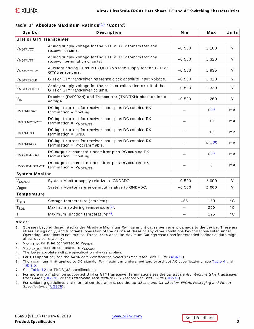
Table 2: Recommended Operating Conditions(1)(2)
Symbol Description Min Typ Max Units
FPGA Logic
VCCINTInternal supply voltage for 0.95V devices. 0.922 0.950 0.979 V
Internal supply voltage for 1.0V devices. 0.970 1.000 1.030 V
VCCINT_IO(3)
Supply voltage for the 0.95V device I/O banks. 0.922 0.950 0.979 V
Supply voltage for the 1.0V device I/O banks. 0.970 1.000 1.030 V
VCCBRAMBlock RAM supply voltage for 0.95V devices. 0.922 0.950 0.979 V
Block RAM supply voltage for 1.0V devices. 0.970 1.000 1.030 V
VCCAUX Auxiliary supply voltage. 1.746 1.800 1.854 V
VCCO(4)(5)
Supply voltage for HR I/O banks. 1.140 – 3.400 V
Supply voltage for HP I/O banks. 0.950 – 1.890 V
VCCAUX_IO(6) Auxiliary I/O supply voltage. 1.746 1.800 1.854 V
VIN(7)
I/O input voltage. –0.200 – VCCO + 0.200 V
I/O input voltage (when VCCO = 3.3V) for VREF and differential I/O standards except TMDS_33(8). – 0.400 2.625 V
IIN(9) Maximum current through any pin in a powered or unpowered bank when forward biasing the clamp diode. – – 10.000 mA
VBATT(10) Battery voltage. 1.000 – 1.890 V
GTH or GTY Transceiver
VMGTAVCC(11)
Analog supply voltage for the GTH transceiver. 0.970 1.000 1.030 V
Analog supply voltage for the GTY transceiver operating at line rates ≤28.21 Gb/s. 0.970 1.000 1.030 V
Analog supply voltage for the GTY transceiver operating at line rates >28.21 Gb/s. 1.000 1.030 1.060 V
VMGTAVTT(11)
Analog supply voltage for the GTH transmitter and receiver termination circuits. 1.170 1.200 1.230 V
Analog supply voltage for GTY receiver and transmitter termination circuits with the transceiver operating at line rates ≤28.21 Gb/s.
1.170 1.200 1.230 V
Analog supply voltage for GTY receiver and transmitter termination circuits with the transceiver operating at line rates >28.21 Gb/s.
1.200 1.230 1.260 V
VMGTVCCAUX(11) Auxiliary analog QPLL voltage supply for the transceivers 1.750 1.800 1.850 V
VMGTAVTTRCAL(11)
Analog supply voltage for the resistor calibration circuit of the GTH transceiver column. 1.170 1.200 1.230 V
Analog supply voltage for the resistor calibration circuit of the GTY transceiver column operating at line rates ≤28.21 Gb/s.
1.170 1.200 1.230 V
Analog supply voltage for the resistor calibration circuit of the GTY transceiver column operating at line rates >28.21 Gb/s.
1.200 1.230 1.260 V
Send Feedback

Virtex UltraScale FPGAs Data Sheet: DC and AC Switching Characteristics
DS893 (v1.10) January 8, 2018 www.xilinx.comProduct Specification 4
SYSMONVCCADC SYSMON supply relative to GNDADC. 1.746 1.800 1.854 V
VREFP Externally supplied reference voltage. 1.200 1.250 1.300 V
Temperature
Tj
Junction temperature operating range for commercial (C) temperature devices. 0 – 85 °C
Junction temperature operating range for extended (E) temperature devices. 0 – 100 °C
Junction temperature operating range for industrial (I) temperature devices. –40 – 100 °C
Notes: 1. All voltages are relative to ground.2. For the design of the power distribution system consult UltraScale Architecture PCB Design Guide (UG583).3. VCCINT_IO must be connected to VCCINT.4. For VCCO_0, the minimum recommended operating voltage for power on and during configuration is 1.425V. After
configuration, data is retained even if VCCO drops to 0V.5. Includes VCCO of 1.0V (HP I/O only), 1.2V, 1.35V, 1.5V, 1.8V, 2.5V (HR I/O only) at ±5%, and 3.3V (HR I/O only) at
+3/–5%.6. VCCAUX_IO must be connected to VCCAUX.7. The lower absolute voltage specification always applies.8. See Table 12 for TMDS_33 specifications.9. A total of 200 mA per 52-pin bank should not be exceeded.10. VBATT is required only when using bitstream encryption. If battery is not used, connect VBATT to either ground or VCCAUX.11. Each voltage listed requires filtering as described in UltraScale Architecture GTH Transceiver User Guide (UG576) or
UltraScale Architecture GTY Transceiver User Guide (UG578).
Table 2: Recommended Operating Conditions(1)(2) (Cont’d)
Symbol Description Min Typ Max Units
Send Feedback

Virtex UltraScale FPGAs Data Sheet: DC and AC Switching Characteristics
DS893 (v1.10) January 8, 2018 www.xilinx.comProduct Specification 5
Table 3: DC Characteristics Over Recommended Operating Conditions
Symbol Description Min Typ(1) Max Units
VDRINTData retention VCCINT voltage (below which configuration data might be lost). 0.82 – – V
VDRAUXData retention VCCAUX voltage (below which configuration data might be lost). 1.50 – – V
IREF VREF leakage current per pin. – – 15 µA
IL Input or output leakage current per pin (sample-tested). – – 15(2) µA
CIN(3)
Die input capacitance at the pad (HP I/O). – – 3.75 pF
Die input capacitance at the pad (HR I/O). – – 7.00 pF
IRPU
Pad pull-up (when selected) at VIN = 0V, VCCO = 3.3V. 75 – 175 µA
Pad pull-up (when selected) at VIN = 0V, VCCO = 2.5V. 50 – 169 µA
Pad pull-up (when selected) at VIN = 0V, VCCO = 1.8V. 60 – 678 µA
Pad pull-up (when selected) at VIN = 0V, VCCO = 1.5V. 30 – 450 µA
Pad pull-up (when selected) at VIN = 0V, VCCO = 1.2V. 10 – 262 µA
IRPDPad pull-down (when selected) at VIN = 3.3V. 60 – 190 µA
Pad pull-down (when selected) at VIN = 1.8V. 29 – 685 µA
ICCADCAnalog supply current, per SYSMON instance, in the powered up state. – – 19.2 mA
IBATT(4) Battery supply current. – – 150 nA
Calibrated programmable on-die termination (DCI) in HP I/O banks(6) (measured per JEDEC specification).
R(7)
Thevenin equivalent resistance of programmable input termination to VCCO/2 where ODT = RTT_40. –10%(5) 40 +10%(5) Ω
Thevenin equivalent resistance of programmable input termination to VCCO/2 where ODT = RTT_48. –10%(5) 48 +10%(5) Ω
Thevenin equivalent resistance of programmable input termination to VCCO/2 where ODT = RTT_60. –10%(5) 60 +10%(5) Ω
Programmable input termination to VCCO where ODT = RTT_40. –10%(5) 40 +10%(5) Ω
Programmable input termination to VCCO where ODT = RTT_48. –10%(5) 48 +10%(5) Ω
Programmable input termination to VCCO where ODT = RTT_60. –10%(5) 60 +10%(5) Ω
Programmable input termination to VCCO where ODT = RTT_120. –10%(5) 120 +10%(5) Ω
Programmable input termination to VCCO where ODT = RTT_240. –10%(5) 240 +10%(5) Ω
Send Feedback

Virtex UltraScale FPGAs Data Sheet: DC and AC Switching Characteristics
DS893 (v1.10) January 8, 2018 www.xilinx.comProduct Specification 6
Uncalibrated programmable on-die termination in HP I/Os banks (measured per JEDEC specification)
R(7)
Thevenin equivalent resistance of programmable input termination to VCCO/2 where ODT = RTT_40. –50% 40 +50% Ω
Thevenin equivalent resistance of programmable input termination to VCCO/2 where ODT = RTT_48. –50% 48 +50% Ω
Thevenin equivalent resistance of programmable input termination to VCCO/2 where ODT = RTT_60. –50% 60 +50% Ω
Programmable input termination to VCCO where ODT = RTT_40. –50% 40 +50% Ω
Programmable input termination to VCCO where ODT = RTT_48. –50% 48 +50% Ω
Programmable input termination to VCCO where ODT = RTT_60. –50% 60 +50% Ω
Programmable input termination to VCCO where ODT = RTT_120. –50% 120 +50% Ω
Programmable input termination to VCCO where ODT = RTT_240. –50% 240 +50% Ω
Uncalibrated programmable on-die termination in HR I/O banks (measured per JEDEC specification).
R(7)
Thevenin equivalent resistance of programmable input termination to VCCO/2 where ODT = RTT_40. –50% 40 +50% Ω
Thevenin equivalent resistance of programmable input termination to VCCO/2 where ODT = RTT_48. –50% 48 +50% Ω
Thevenin equivalent resistance of programmable input termination to VCCO/2 where ODT = RTT_60. –50% 60 +50% Ω
Internal VREF
50% VCCOVCCO x 0.49
VCCO x 0.50
VCCO x 0.51 V
70% VCCOVCCO x 0.69
VCCO x 0.70
VCCO x 0.71 V
Differential termination Programmable differential termination (TERM_100). – 100 – Ω
n Temperature diode ideality factor. – 1.002 – –
r Temperature diode series resistance. – 2 – Ω
Notes: 1. Typical values are specified at nominal voltage, 25°C.2. For HP I/O banks with a VCCO of 1.8V and separated VCCO and VCCAUX_IO power supplies, the IL maximum current is 70 µA.3. This measurement represents the die capacitance at the pad, not including the package.4. Maximum value specified for worst case process at 25°C.5. If VRP resides at a different bank (DCI cascade), the range increases to ±15%.6. VRP resistor tolerance is (240Ω ±1%).7. On-die input termination resistance, for more information see the UltraScale Architecture SelectIO Resources User Guide
(UG571).
Table 3: DC Characteristics Over Recommended Operating Conditions (Cont’d)
Symbol Description Min Typ(1) Max Units
Send Feedback

Virtex UltraScale FPGAs Data Sheet: DC and AC Switching Characteristics
DS893 (v1.10) January 8, 2018 www.xilinx.comProduct Specification 7
Table 4: VIN Maximum Allowed AC Voltage Overshoot and Undershoot for HR I/O Banks(1)(2)
AC Voltage Overshoot % of UI at –40°C to 100°C AC Voltage
Undershoot% of UI at –40°C to
100°CVCCO + 0.30 100% –0.30 100%
VCCO + 0.35 100% –0.35 70.00%
VCCO + 0.40 100% –0.40 27.00%
VCCO + 0.45 100% –0.45 10.00%
VCCO + 0.50 85.00% –0.50 5.00%
VCCO + 0.55 70.00% –0.55 2.10%
VCCO + 0.60 46.60% –0.60 1.50%
VCCO + 0.65 21.20% –0.65 1.10%
VCCO + 0.70 9.75% –0.70 0.60%
VCCO + 0.75 4.55% –0.75 0.45%
VCCO + 0.80 2.15% –0.80 0.20%
VCCO + 0.85 1.00% –0.85 0.10%
VCCO + 0.90 0.50% –0.90 0.05%
Notes: 1. A total of 200 mA per bank should not be exceeded.2. For UI smaller than 20 µs.
Table 5: VIN Maximum Allowed AC Voltage Overshoot and Undershoot for HP I/O Banks(1)(2)
AC Voltage Overshoot % of UI at –40°C to 100°C AC Voltage
Undershoot% of UI at –40°C to
100°CVCCO + 0.05 100% –0.05 100%
VCCO + 0.10 100% –0.10 100%
VCCO + 0.15 100% –0.15 100%
VCCO + 0.20 100% –0.20 100%
VCCO + 0.25 100% –0.25 100%
VCCO + 0.30 100% –0.30 100%
VCCO + 0.35 92.00% –0.35 92.00%
VCCO + 0.40 70.00% –0.40 40.00%
VCCO + 0.45 30.00% –0.45 15.00%
VCCO + 0.50 15.00% –0.50 10.00%
VCCO + 0.55 10.00% –0.55 4.00%
VCCO + 0.60 8.00% –0.60 0.00%
VCCO + 0.65 6.00% –0.65 0.00%
VCCO + 0.70 4.00% –0.70 0.00%
VCCO + 0.75 2.00% –0.75 0.00%
VCCO + 0.80 2.00% –0.80 0.00%
VCCO + 0.85 2.00% –0.85 0.00%
Notes: 1. A total of 200 mA per bank should not be exceeded.2. For UI smaller than 20 µs.
Send Feedback
Virtex UltraScale FPGAs Data Sheet: DC and AC Switching Characteristics
DS893 (v1.10) January 8, 2018 www.xilinx.comProduct Specification 8
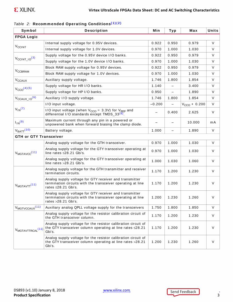
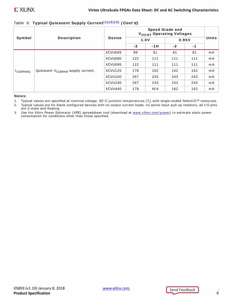
Table 6: Typical Quiescent Supply Current(1)(2)(3)
Symbol Description Device
Speed Grade and VCCINT Operating Voltages
Units1.0V 0.95V
-3 -1H -2 -1
ICCINTQ Quiescent VCCINT supply current.
XCVU065 1581 1437 1437 1437 mA
XCVU080 2309 2100 2100 2100 mA
XCVU095 2309 2100 2100 2100 mA
XCVU125 3161 2875 2875 2875 mA
XCVU160 4742 4312 4312 4312 mA
XCVU190 4742 4312 4312 4312 mA
XCVU440 7988 N/A 7264 7264 mA
ICCINT_IOQ Quiescent current for VCCINT_IO supply.
XCVU065 100 89 89 89 mA
XCVU080 161 143 143 143 mA
XCVU095 161 143 143 143 mA
XCVU125 200 178 178 178 mA
XCVU160 299 266 266 266 mA
XCVU190 299 266 266 266 mA
XCVU440 299 N/A 266 266 mA
ICCOQ Quiescent VCCO supply current.
XCVU065 1 1 1 1 mA
XCVU080 1 1 1 1 mA
XCVU095 1 1 1 1 mA
XCVU125 1 1 1 1 mA
XCVU160 1 1 1 1 mA
XCVU190 1 1 1 1 mA
XCVU440 1 N/A 1 1 mA
ICCAUXQ Quiescent VCCAUX supply current.
XCVU065 187 187 187 187 mA
XCVU080 273 273 273 273 mA
XCVU095 273 273 273 273 mA
XCVU125 373 373 373 373 mA
XCVU160 560 560 560 560 mA
XCVU190 560 560 560 560 mA
XCVU440 1009 N/A 1009 1009 mA
ICCAUX_IOQ Quiescent VCCAUX_IO supply current.
XCVU065 74 74 74 74 mA
XCVU080 124 124 124 124 mA
XCVU095 124 124 124 124 mA
XCVU125 148 148 148 148 mA
XCVU160 223 223 223 223 mA
XCVU190 223 223 223 223 mA
XCVU440 223 N/A 223 223 mA
Send Feedback
Virtex UltraScale FPGAs Data Sheet: DC and AC Switching Characteristics
DS893 (v1.10) January 8, 2018 www.xilinx.comProduct Specification 9
ICCBRAMQ Quiescent VCCBRAM supply current.
XCVU065 89 81 81 81 mA
XCVU080 122 111 111 111 mA
XCVU095 122 111 111 111 mA
XCVU125 178 162 162 162 mA
XCVU160 267 243 243 243 mA
XCVU190 267 243 243 243 mA
XCVU440 178 N/A 162 162 mA
Notes: 1. Typical values are specified at nominal voltage, 85°C junction temperatures (Tj) with single-ended SelectIO™ resources.2. Typical values are for blank configured devices with no output current loads, no active input pull-up resistors, all I/O pins
are 3-state and floating.3. Use the Xilinx Power Estimator (XPE) spreadsheet tool (download at www.xilinx.com/power) to estimate static power
consumption for conditions other than those specified.
Table 6: Typical Quiescent Supply Current(1)(2)(3) (Cont’d)
Symbol Description Device
Speed Grade and VCCINT Operating Voltages
Units1.0V 0.95V
-3 -1H -2 -1
Send Feedback

Virtex UltraScale FPGAs Data Sheet: DC and AC Switching Characteristics
DS893 (v1.10) January 8, 2018 www.xilinx.comProduct Specification 10
Power-On/Off Power Supply SequencingThe recommended power-on sequence is VCCINT/VCCINT_IO, VCCBRAM, VCCAUX/VCCAUX_IO, and VCCO to achieve minimum current draw and ensure that the I/Os are 3-stated at power-on. The recommended power-off sequence is the reverse of the power-on sequence. If VCCINT/VCCINT_IO and VCCBRAM have the same recommended voltage levels, they can be powered by the same supply and ramped simultaneously. VCCINT_IO must be connected to VCCINT. If VCCAUX/VCCAUX_IO and VCCO have the same recommended voltage levels, they can be powered by the same supply and ramped simultaneously. VCCAUX and VCCAUX_IO must be connected together. When the current minimums are met, the device powers on after the VCCINT/VCCINT_IO, VCCBRAM, VCCAUX/VCCAUX_IO, and VCCO_0 supplies have all passed through their power-on reset threshold voltages. The device must not be configured until after VCCINT is applied.
VCCADC and VREF can be powered at any time and have no power-up sequencing recommendations.
The recommended power-on sequence to achieve minimum current draw for the GTH or GTY transceivers is VCCINT, VMGTAVCC, VMGTAVTT OR VMGTAVCC, VCCINT, VMGTAVTT. There is no recommended sequencing for VMGTVCCAUX. Both VMGTAVCC and VCCINT can be ramped simultaneously. The recommended power-off sequence is the reverse of the power-on sequence to achieve minimum current draw. If these recommended sequences are not met, current drawn from VMGTAVTT can be higher than specifications during power-up and power-down.
Send Feedback
Virtex UltraScale FPGAs Data Sheet: DC and AC Switching Characteristics
DS893 (v1.10) January 8, 2018 www.xilinx.comProduct Specification 11
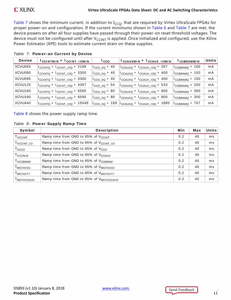
Table 7 shows the minimum current, in addition to ICCQ, that are required by Virtex UltraScale FPGAs for proper power-on and configuration. If the current minimums shown in Table 6 and Table 7 are met, the device powers on after all four supplies have passed through their power-on reset threshold voltages. The device must not be configured until after VCCINT is applied. Once initialized and configured, use the Xilinx Power Estimator (XPE) tools to estimate current drain on these supplies.
Table 8 shows the power supply ramp time.
Table 7: Power-on Current by Device
Device ICCINTMIN + ICCINT_IOMIN ICCO ICCAUXMIN + ICCAUX_IOMIN ICCBRAMMIN UnitsXCVU065 ICCINTQ + ICCINT_IOQ + 2199 ICCO_0Q + 40 ICCAUXQ + ICCAUX_IOQ + 267 ICCBRAMQ + 100 mA
XCVU080 ICCINTQ + ICCINT_IOQ + 3300 ICCO_0Q + 40 ICCAUXQ + ICCAUX_IOQ + 400 ICCBRAMQ + 150 mA
XCVU095 ICCINTQ + ICCINT_IOQ + 3300 ICCO_0Q + 40 ICCAUXQ + ICCAUX_IOQ + 400 ICCBRAMQ + 150 mA
XCVU125 ICCINTQ + ICCINT_IOQ + 4397 ICCO_0Q + 54 ICCAUXQ + ICCAUX_IOQ + 533 ICCBRAMQ + 200 mA
XCVU160 ICCINTQ + ICCINT_IOQ + 6595 ICCO_0Q + 80 ICCAUXQ + ICCAUX_IOQ + 800 ICCBRAMQ + 300 mA
XCVU190 ICCINTQ + ICCINT_IOQ + 6595 ICCO_0Q + 80 ICCAUXQ + ICCAUX_IOQ + 800 ICCBRAMQ + 300 mA
XCVU440 ICCINTQ + ICCINT_IOQ + 15549 ICCO_0Q + 189 ICCAUXQ + ICCAUX_IOQ + 1885 ICCBRAMQ + 707 mA
Table 8: Power Supply Ramp Time
Symbol Description Min Max UnitsTVCCINT Ramp time from GND to 95% of VCCINT. 0.2 40 ms
TVCCINT_IO Ramp time from GND to 95% of VCCINT_IO. 0.2 40 ms
TVCCO Ramp time from GND to 95% of VCCO. 0.2 40 ms
TVCCAUX Ramp time from GND to 95% of VCCAUX. 0.2 40 ms
TVCCBRAM Ramp time from GND to 95% of VCCBRAM. 0.2 40 ms
TMGTAVCC Ramp time from GND to 95% of VMGTAVCC. 0.2 40 ms
TMGTAVTT Ramp time from GND to 95% of VMGTAVTT. 0.2 40 ms
TMGTVCCAUX Ramp time from GND to 95% of VMGTVCCAUX. 0.2 40 ms
Send Feedback

Virtex UltraScale FPGAs Data Sheet: DC and AC Switching Characteristics
DS893 (v1.10) January 8, 2018 www.xilinx.comProduct Specification 12
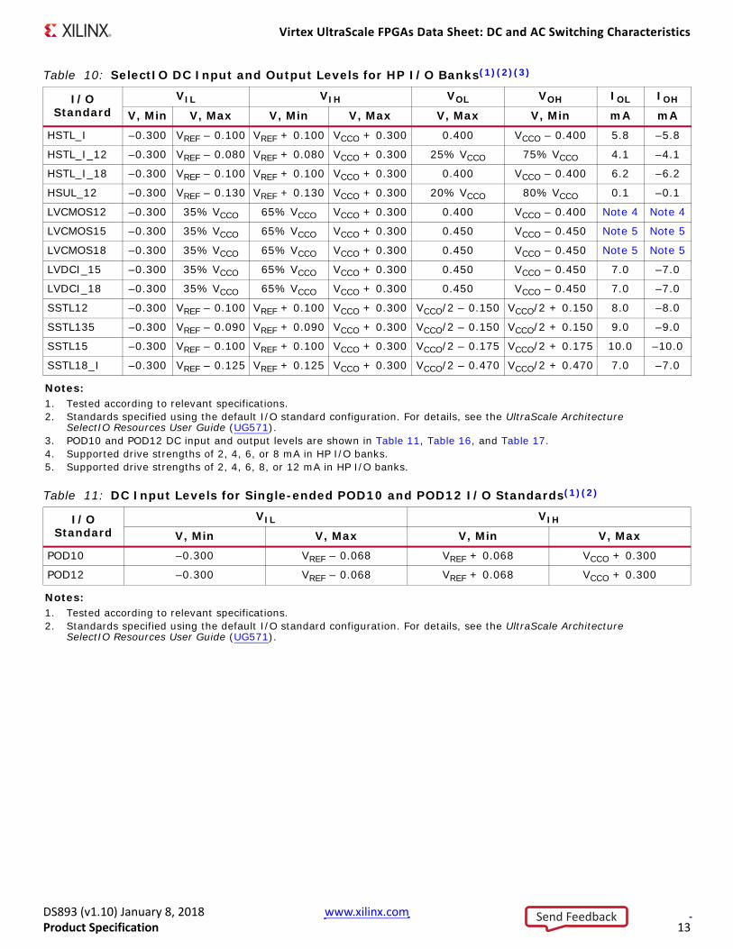
DC Input and Output LevelsValues for VIL and VIH are recommended input voltages. Values for IOL and IOH are guaranteed over the recommended operating conditions at the VOL and VOH test points. Only selected standards are tested. These are chosen to ensure that all standards meet their specifications. The selected standards are tested at a minimum VCCO with the respective VOL and VOH voltage levels shown. Other standards are sample tested.
Table 9: SelectIO DC Input and Output Levels For HR I/O Banks(1)(2)
I/O Standard
VIL VIH VOL VOH IOL IOH
V, Min V, Max V, Min V, Max V, Max V, Min mA mAHSTL_I –0.300 VREF – 0.100 VREF + 0.100 VCCO + 0.300 0.400 VCCO – 0.400 8.0 –8.0
HSTL_I_18 –0.300 VREF – 0.100 VREF + 0.100 VCCO + 0.300 0.400 VCCO – 0.400 8.0 –8.0
HSTL_II –0.300 VREF – 0.100 VREF + 0.100 VCCO + 0.300 0.400 VCCO – 0.400 16.0 –16.0
HSTL_II_18 –0.300 VREF – 0.100 VREF + 0.100 VCCO + 0.300 0.400 VCCO – 0.400 16.0 –16.0
HSUL_12 –0.300 VREF – 0.130 VREF + 0.130 VCCO + 0.300 20% VCCO 80% VCCO 0.1 –0.1
LVCMOS12 –0.300 35% VCCO 65% VCCO VCCO + 0.300 0.400 VCCO – 0.400 Note 3 Note 3
LVCMOS15 –0.300 35% VCCO 65% VCCO VCCO + 0.300 0.450 VCCO – 0.450 Note 4 Note 4
LVCMOS18 –0.300 35% VCCO 65% VCCO VCCO + 0.300 0.450 VCCO – 0.450 Note 4 Note 4
LVCMOS25 –0.300 0.700 1.700 VCCO + 0.300 0.400 VCCO – 0.400 Note 4 Note 4
LVCMOS33 –0.300 0.800 2.000 3.400 0.400 VCCO – 0.400 Note 4 Note 4
LVTTL –0.300 0.800 2.000 3.400 0.400 2.400 Note 4 Note 4
SSTL12 –0.300 VREF – 0.100 VREF + 0.100 VCCO + 0.300 VCCO/2 – 0.150 VCCO/2 + 0.150 14.25 –14.25
SSTL135 –0.300 VREF – 0.090 VREF + 0.090 VCCO + 0.300 VCCO/2 – 0.150 VCCO/2 + 0.150 13.0 –13.0
SSTL135_R –0.300 VREF – 0.090 VREF + 0.090 VCCO + 0.300 VCCO/2 – 0.150 VCCO/2 + 0.150 8.9 –8.9
SSTL15 –0.300 VREF – 0.100 VREF + 0.100 VCCO + 0.300 VCCO/2 – 0.175 VCCO/2 + 0.175 13.0 –13.0
SSTL15_R –0.300 VREF – 0.100 VREF + 0.100 VCCO + 0.300 VCCO/2 – 0.175 VCCO/2 + 0.175 8.9 –8.9
SSTL18_I –0.300 VREF – 0.125 VREF + 0.125 VCCO + 0.300 VCCO/2 – 0.470 VCCO/2 + 0.470 8.0 –8.0
SSTL18_II –0.300 VREF – 0.125 VREF + 0.125 VCCO + 0.300 VCCO/2 – 0.600 VCCO/2 + 0.600 13.4 –13.4
Notes: 1. Tested according to relevant specifications.2. Standards specified using the default I/O standard configuration. For details, see the UltraScale Architecture
SelectIO Resources User Guide (UG571).3. Supported drive strengths of 4, 8, or 12 mA in HR I/O banks.4. Supported drive strengths of 4, 8, 12, or 16 mA in HR I/O banks.
Send Feedback
Virtex UltraScale FPGAs Data Sheet: DC and AC Switching Characteristics
DS893 (v1.10) January 8, 2018 www.xilinx.comProduct Specification 13
Table 10: SelectIO DC Input and Output Levels for HP I/O Banks(1)(2)(3)
I/O Standard
VIL VIH VOL VOH IOL IOH
V, Min V, Max V, Min V, Max V, Max V, Min mA mAHSTL_I –0.300 VREF – 0.100 VREF + 0.100 VCCO + 0.300 0.400 VCCO – 0.400 5.8 –5.8
HSTL_I_12 –0.300 VREF – 0.080 VREF + 0.080 VCCO + 0.300 25% VCCO 75% VCCO 4.1 –4.1
HSTL_I_18 –0.300 VREF – 0.100 VREF + 0.100 VCCO + 0.300 0.400 VCCO – 0.400 6.2 –6.2
HSUL_12 –0.300 VREF – 0.130 VREF + 0.130 VCCO + 0.300 20% VCCO 80% VCCO 0.1 –0.1
LVCMOS12 –0.300 35% VCCO 65% VCCO VCCO + 0.300 0.400 VCCO – 0.400 Note 4 Note 4
LVCMOS15 –0.300 35% VCCO 65% VCCO VCCO + 0.300 0.450 VCCO – 0.450 Note 5 Note 5
LVCMOS18 –0.300 35% VCCO 65% VCCO VCCO + 0.300 0.450 VCCO – 0.450 Note 5 Note 5
LVDCI_15 –0.300 35% VCCO 65% VCCO VCCO + 0.300 0.450 VCCO – 0.450 7.0 –7.0
LVDCI_18 –0.300 35% VCCO 65% VCCO VCCO + 0.300 0.450 VCCO – 0.450 7.0 –7.0
SSTL12 –0.300 VREF – 0.100 VREF + 0.100 VCCO + 0.300 VCCO/2 – 0.150 VCCO/2 + 0.150 8.0 –8.0
SSTL135 –0.300 VREF – 0.090 VREF + 0.090 VCCO + 0.300 VCCO/2 – 0.150 VCCO/2 + 0.150 9.0 –9.0
SSTL15 –0.300 VREF – 0.100 VREF + 0.100 VCCO + 0.300 VCCO/2 – 0.175 VCCO/2 + 0.175 10.0 –10.0
SSTL18_I –0.300 VREF – 0.125 VREF + 0.125 VCCO + 0.300 VCCO/2 – 0.470 VCCO/2 + 0.470 7.0 –7.0
Notes: 1. Tested according to relevant specifications.2. Standards specified using the default I/O standard configuration. For details, see the UltraScale Architecture
SelectIO Resources User Guide (UG571).3. POD10 and POD12 DC input and output levels are shown in Table 11, Table 16, and Table 17.4. Supported drive strengths of 2, 4, 6, or 8 mA in HP I/O banks.5. Supported drive strengths of 2, 4, 6, 8, or 12 mA in HP I/O banks.
Table 11: DC Input Levels for Single-ended POD10 and POD12 I/O Standards(1)(2)
I/O Standard
VIL VIH
V, Min V, Max V, Min V, MaxPOD10 –0.300 VREF – 0.068 VREF + 0.068 VCCO + 0.300
POD12 –0.300 VREF – 0.068 VREF + 0.068 VCCO + 0.300
Notes: 1. Tested according to relevant specifications.2. Standards specified using the default I/O standard configuration. For details, see the UltraScale Architecture
SelectIO Resources User Guide (UG571).
Send Feedback
Virtex UltraScale FPGAs Data Sheet: DC and AC Switching Characteristics
DS893 (v1.10) January 8, 2018 www.xilinx.comProduct Specification 14
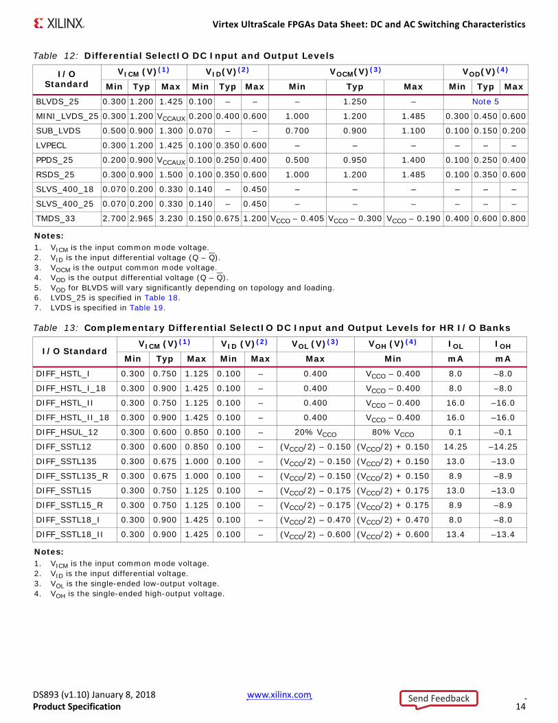
Table 12: Differential SelectIO DC Input and Output Levels
I/O Standard
VICM (V)(1) VID(V)(2) VOCM(V)(3) VOD(V)(4)
Min Typ Max Min Typ Max Min Typ Max Min Typ MaxBLVDS_25 0.300 1.200 1.425 0.100 – – – 1.250 – Note 5
MINI_LVDS_25 0.300 1.200 VCCAUX 0.200 0.400 0.600 1.000 1.200 1.485 0.300 0.450 0.600
SUB_LVDS 0.500 0.900 1.300 0.070 – – 0.700 0.900 1.100 0.100 0.150 0.200
LVPECL 0.300 1.200 1.425 0.100 0.350 0.600 – – – – – –
PPDS_25 0.200 0.900 VCCAUX 0.100 0.250 0.400 0.500 0.950 1.400 0.100 0.250 0.400
RSDS_25 0.300 0.900 1.500 0.100 0.350 0.600 1.000 1.200 1.485 0.100 0.350 0.600
SLVS_400_18 0.070 0.200 0.330 0.140 – 0.450 – – – – – –
SLVS_400_25 0.070 0.200 0.330 0.140 – 0.450 – – – – – –
TMDS_33 2.700 2.965 3.230 0.150 0.675 1.200 VCCO – 0.405 VCCO – 0.300 VCCO – 0.190 0.400 0.600 0.800
Notes: 1. VICM is the input common mode voltage.2. VID is the input differential voltage (Q – Q).3. VOCM is the output common mode voltage.4. VOD is the output differential voltage (Q – Q).5. VOD for BLVDS will vary significantly depending on topology and loading.6. LVDS_25 is specified in Table 18.7. LVDS is specified in Table 19.
Table 13: Complementary Differential SelectIO DC Input and Output Levels for HR I/O Banks
I/O StandardVICM (V)(1) VID (V)(2) VOL (V)(3) VOH (V)(4) IOL IOH
Min Typ Max Min Max Max Min mA mADIFF_HSTL_I 0.300 0.750 1.125 0.100 – 0.400 VCCO – 0.400 8.0 –8.0
DIFF_HSTL_I_18 0.300 0.900 1.425 0.100 – 0.400 VCCO – 0.400 8.0 –8.0
DIFF_HSTL_II 0.300 0.750 1.125 0.100 – 0.400 VCCO – 0.400 16.0 –16.0
DIFF_HSTL_II_18 0.300 0.900 1.425 0.100 – 0.400 VCCO – 0.400 16.0 –16.0
DIFF_HSUL_12 0.300 0.600 0.850 0.100 – 20% VCCO 80% VCCO 0.1 –0.1
DIFF_SSTL12 0.300 0.600 0.850 0.100 – (VCCO/2) – 0.150 (VCCO/2) + 0.150 14.25 –14.25
DIFF_SSTL135 0.300 0.675 1.000 0.100 – (VCCO/2) – 0.150 (VCCO/2) + 0.150 13.0 –13.0
DIFF_SSTL135_R 0.300 0.675 1.000 0.100 – (VCCO/2) – 0.150 (VCCO/2) + 0.150 8.9 –8.9
DIFF_SSTL15 0.300 0.750 1.125 0.100 – (VCCO/2) – 0.175 (VCCO/2) + 0.175 13.0 –13.0
DIFF_SSTL15_R 0.300 0.750 1.125 0.100 – (VCCO/2) – 0.175 (VCCO/2) + 0.175 8.9 –8.9
DIFF_SSTL18_I 0.300 0.900 1.425 0.100 – (VCCO/2) – 0.470 (VCCO/2) + 0.470 8.0 –8.0
DIFF_SSTL18_II 0.300 0.900 1.425 0.100 – (VCCO/2) – 0.600 (VCCO/2) + 0.600 13.4 –13.4
Notes: 1. VICM is the input common mode voltage.2. VID is the input differential voltage.3. VOL is the single-ended low-output voltage.4. VOH is the single-ended high-output voltage.
Send Feedback

Virtex UltraScale FPGAs Data Sheet: DC and AC Switching Characteristics
DS893 (v1.10) January 8, 2018 www.xilinx.comProduct Specification 15
Table 14: Complementary Differential SelectIO DC Input and Output Levels for HP I/O Banks(1)
I/O StandardVICM (V)(2) VID (V)(3) VOL (V)(4) VOH (V)(5) IOL IOH
Min Typ Max Min Max Max Min mA mADIFF_HSTL_I 0.680 VCCO/2 (VCCO/2) + 0.150 0.100 – 0.400 VCCO – 0.400 5.8 –5.8
DIFF_HSTL_I_12 0.400 x VCCO VCCO/2 0.600 x VCCO 0.100 – 0.250 x VCCO 0.750 x VCCO 4.1 –4.1
DIFF_HSTL_I_18 (VCCO/2) – 0.175 VCCO/2 (VCCO/2) + 0.175 0.100 – 0.400 VCCO – 0.400 6.2 –6.2
DIFF_HSUL_12 (VCCO/2) – 0.120 VCCO/2 (VCCO/2) + 0.120 0.100 – 20% VCCO 80% VCCO 0.1 –0.1
DIFF_SSTL12 (VCCO/2) – 0.150 VCCO/2 (VCCO/2) + 0.150 0.100 – (VCCO/2) – 0.150 (VCCO/2) + 0.150 8.0 –8.0
DIFF_SSTL135 (VCCO/2) – 0.150 VCCO/2 (VCCO/2) + 0.150 0.100 – (VCCO/2) – 0.150 (VCCO/2) + 0.150 9.0 –9.0
DIFF_SSTL15 (VCCO/2) – 0.175 VCCO/2 (VCCO/2) + 0.175 0.100 – (VCCO/2) – 0.175 (VCCO/2) + 0.175 10.0 –10.0
DIFF_SSTL18_I (VCCO/2) – 0.175 VCCO/2 (VCCO/2) + 0.175 0.100 – (VCCO/2) – 0.470 (VCCO/2) + 0.470 7.0 –7.0
Notes: 1. DIFF_POD10 and DIFF_POD12 HP I/O bank specifications are shown in Table 15, Table 16, and Table 17.2. VICM is the input common mode voltage.3. VID is the input differential voltage.4. VOL is the single-ended low-output voltage.5. VOH is the single-ended high-output voltage.
Table 15: DC Input Levels for Differential POD10 and POD12 I/O Standards(1)(2)
I/O StandardVICM (V) VID (V)
Min Typ Max Min MaxDIFF_POD10 0.63 0.70 0.77 0.14 –
DIFF_POD12 0.76 0.84 0.92 0.16 –
Notes: 1. Tested according to relevant specifications.2. Standards specified using the default I/O standard configuration. For details, see the UltraScale Architecture
SelectIO Resources User Guide (UG571).
Table 16: DC Output Levels for Single-ended and Differential POD10 and POD12 Standards(1)(2)
Symbol Description VOUT Min Typ Max UnitsROL Pull-down resistance VOM_DC (as described in Table 17) 36 40 44 Ω
ROH Pull-up resistance VOM_DC (as described in Table 17) 36 40 44 Ω
Notes: 1. Tested according to relevant specifications.2. Standards specified using the default I/O standard configuration. For details, see the UltraScale Architecture
SelectIO Resources User Guide (UG571).
Table 17: Table 16 Definitions for DC Output Levels for POD Standards
Symbol Description All Devices UnitsVOM_DC DC output Mid measurement level (for IV curve linearity). 0.8 x VCCO V
Send Feedback
Virtex UltraScale FPGAs Data Sheet: DC and AC Switching Characteristics
DS893 (v1.10) January 8, 2018 www.xilinx.comProduct Specification 16
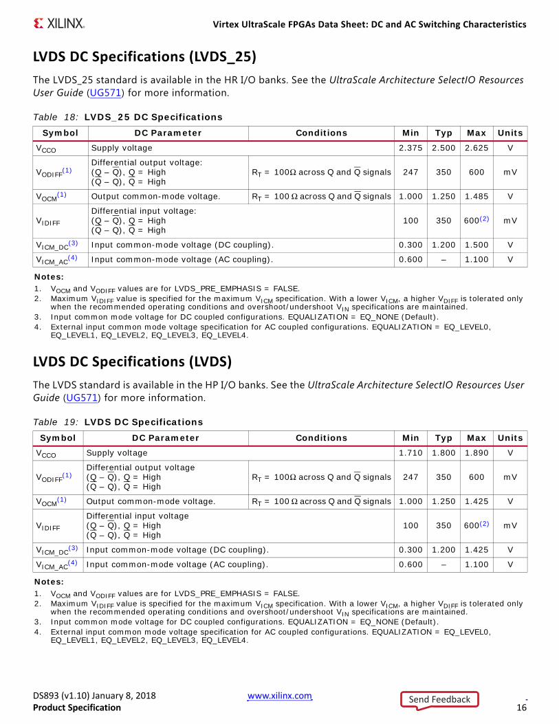
LVDS DC Specifications (LVDS_25)The LVDS_25 standard is available in the HR I/O banks. See the UltraScale Architecture SelectIO Resources User Guide (UG571) for more information.
LVDS DC Specifications (LVDS)The LVDS standard is available in the HP I/O banks. See the UltraScale Architecture SelectIO Resources User Guide (UG571) for more information.
Table 18: LVDS_25 DC Specifications
Symbol DC Parameter Conditions Min Typ Max UnitsVCCO Supply voltage 2.375 2.500 2.625 V
VODIFF(1)
Differential output voltage:(Q – Q), Q = High (Q – Q), Q = High
RT = 100Ω across Q and Q signals 247 350 600 mV
VOCM(1) Output common-mode voltage. RT = 100 Ω across Q and Q signals 1.000 1.250 1.485 V
VIDIFF
Differential input voltage:(Q – Q), Q = High (Q – Q), Q = High
100 350 600(2) mV
VICM_DC(3) Input common-mode voltage (DC coupling). 0.300 1.200 1.500 V
VICM_AC(4) Input common-mode voltage (AC coupling). 0.600 – 1.100 V
Notes: 1. VOCM and VODIFF values are for LVDS_PRE_EMPHASIS = FALSE.2. Maximum VIDIFF value is specified for the maximum VICM specification. With a lower VICM, a higher VDIFF is tolerated only
when the recommended operating conditions and overshoot/undershoot VIN specifications are maintained.3. Input common mode voltage for DC coupled configurations. EQUALIZATION = EQ_NONE (Default).4. External input common mode voltage specification for AC coupled configurations. EQUALIZATION = EQ_LEVEL0,
EQ_LEVEL1, EQ_LEVEL2, EQ_LEVEL3, EQ_LEVEL4.
Table 19: LVDS DC Specifications
Symbol DC Parameter Conditions Min Typ Max UnitsVCCO Supply voltage 1.710 1.800 1.890 V
VODIFF(1)
Differential output voltage(Q – Q), Q = High (Q – Q), Q = High
RT = 100Ω across Q and Q signals 247 350 600 mV
VOCM(1) Output common-mode voltage. RT = 100 Ω across Q and Q signals 1.000 1.250 1.425 V
VIDIFF
Differential input voltage(Q – Q), Q = High (Q – Q), Q = High
100 350 600(2) mV
VICM_DC(3) Input common-mode voltage (DC coupling). 0.300 1.200 1.425 V
VICM_AC(4) Input common-mode voltage (AC coupling). 0.600 – 1.100 V
Notes: 1. VOCM and VODIFF values are for LVDS_PRE_EMPHASIS = FALSE.2. Maximum VIDIFF value is specified for the maximum VICM specification. With a lower VICM, a higher VDIFF is tolerated only
when the recommended operating conditions and overshoot/undershoot VIN specifications are maintained.3. Input common mode voltage for DC coupled configurations. EQUALIZATION = EQ_NONE (Default).4. External input common mode voltage specification for AC coupled configurations. EQUALIZATION = EQ_LEVEL0,
EQ_LEVEL1, EQ_LEVEL2, EQ_LEVEL3, EQ_LEVEL4.
Send Feedback
Virtex UltraScale FPGAs Data Sheet: DC and AC Switching Characteristics
DS893 (v1.10) January 8, 2018 www.xilinx.comProduct Specification 17
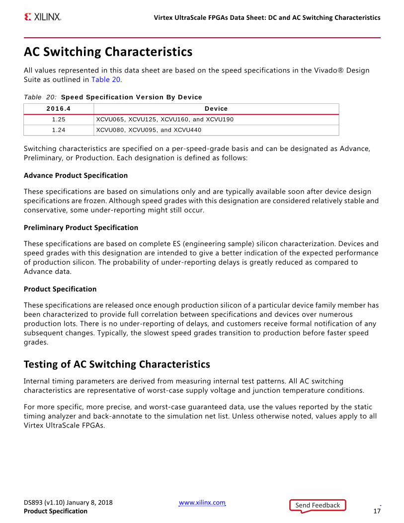
AC Switching CharacteristicsAll values represented in this data sheet are based on the speed specifications in the Vivado® Design Suite as outlined in Table 20.
Switching characteristics are specified on a per-speed-grade basis and can be designated as Advance, Preliminary, or Production. Each designation is defined as follows:
Advance Product Specification
These specifications are based on simulations only and are typically available soon after device design specifications are frozen. Although speed grades with this designation are considered relatively stable and conservative, some under-reporting might still occur.
Preliminary Product Specification
These specifications are based on complete ES (engineering sample) silicon characterization. Devices and speed grades with this designation are intended to give a better indication of the expected performance of production silicon. The probability of under-reporting delays is greatly reduced as compared to Advance data.
Product Specification
These specifications are released once enough production silicon of a particular device family member has been characterized to provide full correlation between specifications and devices over numerous production lots. There is no under-reporting of delays, and customers receive formal notification of any subsequent changes. Typically, the slowest speed grades transition to production before faster speed grades.
Testing of AC Switching CharacteristicsInternal timing parameters are derived from measuring internal test patterns. All AC switching characteristics are representative of worst-case supply voltage and junction temperature conditions.
For more specific, more precise, and worst-case guaranteed data, use the values reported by the static timing analyzer and back-annotate to the simulation net list. Unless otherwise noted, values apply to all Virtex UltraScale FPGAs.
Table 20: Speed Specification Version By Device
2016.4 Device1.25 XCVU065, XCVU125, XCVU160, and XCVU190
1.24 XCVU080, XCVU095, and XCVU440
Send Feedback
Virtex UltraScale FPGAs Data Sheet: DC and AC Switching Characteristics
DS893 (v1.10) January 8, 2018 www.xilinx.comProduct Specification 18
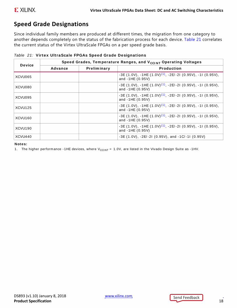
Speed Grade DesignationsSince individual family members are produced at different times, the migration from one category to another depends completely on the status of the fabrication process for each device. Table 21 correlates the current status of the Virtex UltraScale FPGAs on a per speed grade basis.
Table 21: Virtex UltraScale FPGAs Speed Grade Designations
DeviceSpeed Grades, Temperature Ranges, and VCCINT Operating Voltages
Advance Preliminary Production
XCVU065 -3E (1.0V), -1HE (1.0V)(1), -2E/-2I (0.95V), -1I (0.95V), and -1HE (0.95V)
XCVU080 -3E (1.0V), -1HE (1.0V)(1), -2E/-2I (0.95V), -1I (0.95V), and -1HE (0.95V)
XCVU095 -3E (1.0V), -1HE (1.0V)(1), -2E/-2I (0.95V), -1I (0.95V), and -1HE (0.95V)
XCVU125 -3E (1.0V), -1HE (1.0V)(1), -2E/-2I (0.95V), -1I (0.95V), and -1HE (0.95V)
XCVU160 -3E (1.0V), -1HE (1.0V)(1), -2E/-2I (0.95V), -1I (0.95V), and -1HE (0.95V)
XCVU190 -3E (1.0V), -1HE (1.0V)(1), -2E/-2I (0.95V), -1I (0.95V), and -1HE (0.95V)
XCVU440 -3E (1.0V), -2E/-2I (0.95V), and -1C/-1I (0.95V)
Notes: 1. The higher performance -1HE devices, where VCCINT = 1.0V, are listed in the Vivado Design Suite as -1HV.
Send Feedback
Virtex UltraScale FPGAs Data Sheet: DC and AC Switching Characteristics
DS893 (v1.10) January 8, 2018 www.xilinx.comProduct Specification 19
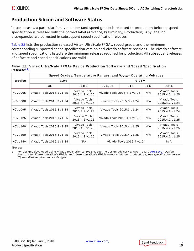
Production Silicon and Software StatusIn some cases, a particular family member (and speed grade) is released to production before a speed specification is released with the correct label (Advance, Preliminary, Production). Any labeling discrepancies are corrected in subsequent speed specification releases.
Table 22 lists the production released Virtex UltraScale FPGAs, speed grade, and the minimum corresponding supported speed specification version and Vivado software revisions. The Vivado software and speed specifications listed are the minimum releases required for production. All subsequent releases of software and speed specifications are valid.
Table 22: Virtex UltraScale FPGAs Device Production Software and Speed Specification Release(1)
Device
Speed Grades, Temperature Ranges, and VCCINT Operating Voltages
1.0V 0.95V
-3E -1HE -2E, -2I -1I -1C -1HE
XCVU065 Vivado Tools 2016.1 v1.25 Vivado Tools 2015.4.2 v1.25 Vivado Tools 2015.4.1 v1.25 N/A Vivado Tools
2015.4.2 v1.25
XCVU080 Vivado Tools 2015.3 v1.24 Vivado Tools 2015.4.2 v1.24 Vivado Tools 2015.3 v1.24 N/A Vivado Tools
2015.4.2 v1.24
XCVU095 Vivado Tools 2015.3 v1.24 Vivado Tools 2015.4.2 v1.24 Vivado Tools 2015.3 v1.24 N/A Vivado Tools
2015.4.2 v1.24
XCVU125 Vivado Tools 2016.1 v1.25 Vivado Tools 2015.4.2 v1.25 Vivado Tools 2015.4.1 v1.25 N/A Vivado Tools
2015.4.2 v1.25
XCVU160 Vivado Tools 2015.4 v1.25 Vivado Tools 2015.4.2 v1.25 Vivado Tools 2015.4 v1.25 N/A Vivado Tools
2015.4.2 v1.25
XCVU190 Vivado Tools 2015.4 v1.25 Vivado Tools 2015.4.2 v1.25 Vivado Tools 2015.4 v1.25 N/A Vivado Tools
2015.4.2 v1.25
XCVU440 Vivado Tools 2016.1 v1.24 N/A Vivado Tools 2015.4 v1.24 N/A
Notes: 1. For designs developed using Vivado tools prior to 2016.4, see the design advisory answer record AR68169: Design
Advisory for Kintex UltraScale FPGAs and Virtex UltraScale FPGAs—New minimum production speed specification version (Speed File) required for all designs.
Send Feedback

Virtex UltraScale FPGAs Data Sheet: DC and AC Switching Characteristics
DS893 (v1.10) January 8, 2018 www.xilinx.comProduct Specification 20
Performance CharacteristicsThis section provides the performance characteristics of some common functions and designs implemented in Virtex UltraScale FPGAs. These values are subject to the same guidelines as the AC Switching Characteristics, page 17. In each table, the I/O bank type is either high performance (HP) or high range (HR).
Table 23: LVDS Component Mode Performance
DescriptionI/O
Bank Type
Speed Grades and VCCINT Operating Voltages
Units1.0V 0.95V
-3 -1H -2 -1
Min Min Max Min Max Min Max Min
LVDS TX DDR (OSERDES 4:1, 8:1)HP 0 1250 0 1250 0 1250 0 1250 Mb/s
HR 0 1250 0 1250 0 1250 0 1000 Mb/s
LVDS TX SDR (OSERDES 2:1, 4:1)HP 0 625 0 625 0 625 0 625 Mb/s
HR 0 625 0 625 0 625 0 500 Mb/s
LVDS RX DDR (ISERDES 1:4, 1:8)(1)HP 0 1250 0 1250 0 1250 0 1250 Mb/s
HR 0 1250 0 1250 0 1250 0 1000 Mb/s
LVDS RX SDR (ISERDES 1:2, 1:4)(1)HP 0 625 0 625 0 625 0 625 Mb/s
HR 0 625 0 625 0 625 0 500 Mb/s
Notes: 1. LVDS receivers are typically bounded with certain applications where specific dynamic phase-alignment (DPA) or
phase-tracking algorithms are used to achieve maximum performance.
Table 24: LVDS Native Mode Performance(1)
DescriptionI/O
Bank Type
Speed Grades and VCCINT Operating Voltages
Units1.0V 0.95V
-3 -1H -2 -1
Min Max Min Max Min Max Min Max
LVDS TX DDR (TX_BITSLICE 4:1, 8:1)HP 300 1600 300 1600 300 1600 300 1400 Mb/sHR 300 1250 300 1250 300 1250 300 1250 Mb/s
LVDS TX SDR (TX_BITSLICE 2:1, 4:1)HP 150 800 150 800 150 800 150 700 Mb/sHR 150 625 150 625 150 625 150 625 Mb/s
LVDS RX DDR (RX_BITSLICE 1:4, 1:8)(2) HP 300 1600 300 1600 300 1600 300 1400 Mb/sHR 300 1250 300 1250 300 1250 300 1250 Mb/s
LVDS RX SDR (RX_BITSLICE 1:2, 1:4)(2) HP 150 800 150 800 150 800 150 700 Mb/sHR 150 625 150 625 150 625 150 625 Mb/s
Notes: 1. Native mode is supported through the High-Speed SelectIO Interface Wizard available with the Vivado Design Suite.2. LVDS receivers are typically bounded with certain applications where specific dynamic phase-alignment (DPA) or
phase-tracking algorithms are used to achieve maximum performance.
Send Feedback

Virtex UltraScale FPGAs Data Sheet: DC and AC Switching Characteristics
DS893 (v1.10) January 8, 2018 www.xilinx.comProduct Specification 21
Table 26 provides the maximum data rates for applicable memory standards using the Virtex UltraScale FPGAs memory PHY. Refer to Memory Interfaces for the complete list of memory interface standards supported and detailed specifications. The final performance of the memory interface is determined through a complete design implemented in the Vivado Design Suite, following guidelines in the UltraScale Architecture PCB Design Guide (UG583), electrical analysis, and characterization of the system.
Table 25: LVDS Native-Mode 1000BASE-X Support(1)
Description I/O Bank Type
Speed Grades and VCCINT Operating Voltages
1.0V 0.95V
-3 -1H -2 -11000BASE-X HP Yes Yes Yes Yes
Notes: 1. 1000BASE-X support is based on the IEEE Standard for CSMA/CD Access Method and Physical Layer Specifications (IEEE
Std 802.3-2008).
Table 26: Maximum Physical Interface (PHY) Rate for Memory Interfaces (HP I/O Banks Only)
Memory Standard DRAM Type
Speed Grades and VCCINT Operating Voltages
Units1.0V 0.95V
-3 -1H -2 -1
DDR4
Single rank component 2400(1) 2400 2400(1) 2133 Mb/s
1 rank DIMM(2)(3) 2133 2133 2133 1866 Mb/s
2 rank DIMM(2)(4) 1866 1866 1866 1600 Mb/s
4 rank DIMM(2)(5) 1333 1333 1333 N/A Mb/s
DDR3
Single rank component 2133 2133 2133 1866 Mb/s
1 rank DIMM(2)(3) 1866 1866 1866 1600 Mb/s
2 rank DIMM(2)(4) 1600 1600 1600 1333 Mb/s
4 rank DIMM(2)(5) 1066 1066 1066 800 Mb/s
DDR3L
Single rank component 1866 1866 1866 1600 Mb/s
1 rank DIMM(2)(3) 1600 1600 1600 1333 Mb/s
2 rank DIMM(2)(4) 1333 1333 1333 1066 Mb/s
4 rank DIMM(2)(5) 800 800 800 606 Mb/s
QDRII+(6) Single rank component 633 600 600 550 MHz
QDRIV-XP Single rank component 800 800 800 667 MHz
RLDRAM III Single rank component 1066 1066 1066 933 MHz
LPDDR3 Single rank component 1600 1600 1600 1600 Mb/s
Notes: 1. The XCVU440 supports a maximum of 15 banks of DDR4 memory at 2400 Mb/s, all other memory rates or configurations
can utilize all the banks.2. Dual in-line memory module (DIMM) includes RDIMM, SODIMM, UDIMM, and LRDIMM.3. Includes: 1 rank 1 slot, DDP 2 rank, LRDIMM 2 or 4 rank 1 slot.4. Includes: 2 rank 1 slot, 1 rank 2 slot, LRDIMM 2 rank 2 slot.5. Includes: 2 rank 2 slot, 4 rank 1 slot.6. The QDRII+ performance specifications are for burst-length 4 (BL = 4) implementations.
Send Feedback
Virtex UltraScale FPGAs Data Sheet: DC and AC Switching Characteristics
DS893 (v1.10) January 8, 2018 www.xilinx.comProduct Specification 22
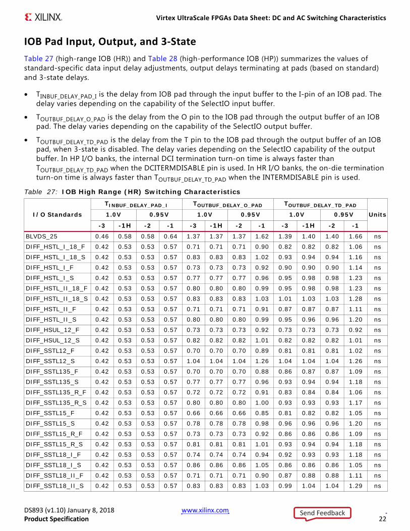
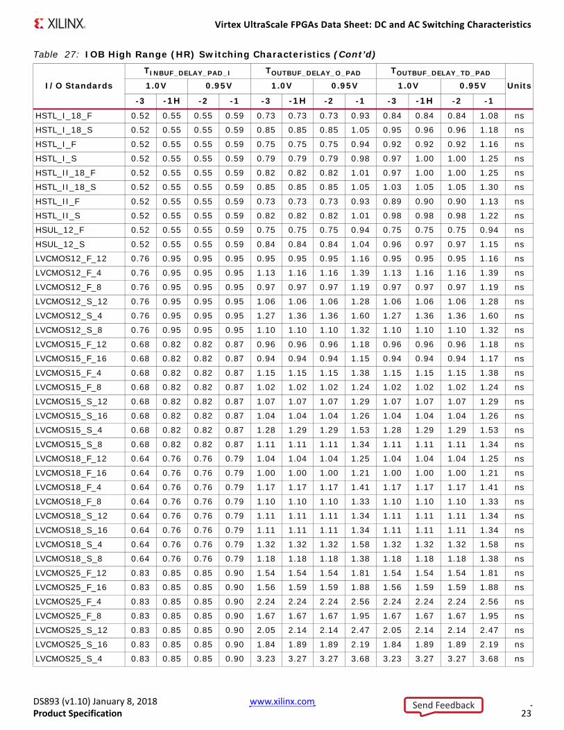
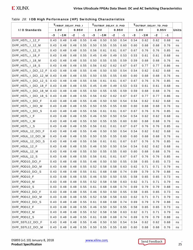
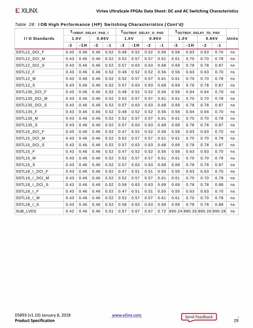
IOB Pad Input, Output, and 3-StateTable 27 (high-range IOB (HR)) and Table 28 (high-performance IOB (HP)) summarizes the values of standard-specific data input delay adjustments, output delays terminating at pads (based on standard) and 3-state delays.
• TINBUF_DELAY_PAD_I is the delay from IOB pad through the input buffer to the I-pin of an IOB pad. The delay varies depending on the capability of the SelectIO input buffer.
• TOUTBUF_DELAY_O_PAD is the delay from the O pin to the IOB pad through the output buffer of an IOB pad. The delay varies depending on the capability of the SelectIO output buffer.
• TOUTBUF_DELAY_TD_PAD is the delay from the T pin to the IOB pad through the output buffer of an IOB pad, when 3-state is disabled. The delay varies depending on the SelectIO capability of the output buffer. In HP I/O banks, the internal DCI termination turn-on time is always faster than TOUTBUF_DELAY_TD_PAD when the DCITERMDISABLE pin is used. In HR I/O banks, the on-die termination turn-on time is always faster than TOUTBUF_DELAY_TD_PAD when the INTERMDISABLE pin is used.
Table 27: IOB High Range (HR) Switching Characteristics
I/O Standards
TINBUF_DELAY_PAD_I TOUTBUF_DELAY_O_PAD TOUTBUF_DELAY_TD_PAD
Units1.0V 0.95V 1.0V 0.95V 1.0V 0.95V
-3 -1H -2 -1 -3 -1H -2 -1 -3 -1H -2 -1
BLVDS_25 0.46 0.58 0.58 0.64 1.37 1.37 1.37 1.62 1.39 1.40 1.40 1.66 ns
DIFF_HSTL_I_18_F 0.42 0.53 0.53 0.57 0.71 0.71 0.71 0.90 0.82 0.82 0.82 1.06 ns
DIFF_HSTL_I_18_S 0.42 0.53 0.53 0.57 0.83 0.83 0.83 1.02 0.93 0.94 0.94 1.16 ns
DIFF_HSTL_I_F 0.42 0.53 0.53 0.57 0.73 0.73 0.73 0.92 0.90 0.90 0.90 1.14 ns
DIFF_HSTL_I_S 0.42 0.53 0.53 0.57 0.77 0.77 0.77 0.96 0.95 0.98 0.98 1.23 ns
DIFF_HSTL_II_18_F 0.42 0.53 0.53 0.57 0.80 0.80 0.80 0.99 0.95 0.98 0.98 1.23 ns
DIFF_HSTL_II_18_S 0.42 0.53 0.53 0.57 0.83 0.83 0.83 1.03 1.01 1.03 1.03 1.28 ns
DIFF_HSTL_II_F 0.42 0.53 0.53 0.57 0.71 0.71 0.71 0.91 0.87 0.87 0.87 1.11 ns
DIFF_HSTL_II_S 0.42 0.53 0.53 0.57 0.80 0.80 0.80 0.99 0.95 0.96 0.96 1.20 ns
DIFF_HSUL_12_F 0.42 0.53 0.53 0.57 0.73 0.73 0.73 0.92 0.73 0.73 0.73 0.92 ns
DIFF_HSUL_12_S 0.42 0.53 0.53 0.57 0.82 0.82 0.82 1.01 0.82 0.82 0.82 1.01 ns
DIFF_SSTL12_F 0.42 0.53 0.53 0.57 0.70 0.70 0.70 0.89 0.81 0.81 0.81 1.02 ns
DIFF_SSTL12_S 0.42 0.53 0.53 0.57 1.04 1.04 1.04 1.26 1.04 1.04 1.04 1.26 ns
DIFF_SSTL135_F 0.42 0.53 0.53 0.57 0.70 0.70 0.70 0.88 0.86 0.87 0.87 1.09 ns
DIFF_SSTL135_S 0.42 0.53 0.53 0.57 0.77 0.77 0.77 0.96 0.93 0.94 0.94 1.18 ns
DIFF_SSTL135_R_F 0.42 0.53 0.53 0.57 0.72 0.72 0.72 0.91 0.83 0.84 0.84 1.06 ns
DIFF_SSTL135_R_S 0.42 0.53 0.53 0.57 0.80 0.80 0.80 1.00 0.93 0.93 0.93 1.17 ns
DIFF_SSTL15_F 0.42 0.53 0.53 0.57 0.66 0.66 0.66 0.85 0.81 0.82 0.82 1.05 ns
DIFF_SSTL15_S 0.42 0.53 0.53 0.57 0.78 0.78 0.78 0.98 0.96 0.96 0.96 1.20 ns
DIFF_SSTL15_R_F 0.42 0.53 0.53 0.57 0.73 0.73 0.73 0.92 0.86 0.86 0.86 1.09 ns
DIFF_SSTL15_R_S 0.42 0.53 0.53 0.57 0.81 0.81 0.81 1.01 0.93 0.94 0.94 1.18 ns
DIFF_SSTL18_I_F 0.42 0.53 0.53 0.57 0.74 0.74 0.74 0.94 0.92 0.93 0.93 1.18 ns
DIFF_SSTL18_I_S 0.42 0.53 0.53 0.57 0.86 0.86 0.86 1.05 0.86 0.86 0.86 1.05 ns
DIFF_SSTL18_II_F 0.42 0.53 0.53 0.57 0.71 0.71 0.71 0.90 0.87 0.88 0.88 1.11 ns
DIFF_SSTL18_II_S 0.42 0.53 0.53 0.57 0.83 0.83 0.83 1.03 0.99 1.04 1.04 1.29 ns
Send Feedback
Virtex UltraScale FPGAs Data Sheet: DC and AC Switching Characteristics
DS893 (v1.10) January 8, 2018 www.xilinx.comProduct Specification 23
HSTL_I_18_F 0.52 0.55 0.55 0.59 0.73 0.73 0.73 0.93 0.84 0.84 0.84 1.08 ns
HSTL_I_18_S 0.52 0.55 0.55 0.59 0.85 0.85 0.85 1.05 0.95 0.96 0.96 1.18 ns
HSTL_I_F 0.52 0.55 0.55 0.59 0.75 0.75 0.75 0.94 0.92 0.92 0.92 1.16 ns
HSTL_I_S 0.52 0.55 0.55 0.59 0.79 0.79 0.79 0.98 0.97 1.00 1.00 1.25 ns
HSTL_II_18_F 0.52 0.55 0.55 0.59 0.82 0.82 0.82 1.01 0.97 1.00 1.00 1.25 ns
HSTL_II_18_S 0.52 0.55 0.55 0.59 0.85 0.85 0.85 1.05 1.03 1.05 1.05 1.30 ns
HSTL_II_F 0.52 0.55 0.55 0.59 0.73 0.73 0.73 0.93 0.89 0.90 0.90 1.13 ns
HSTL_II_S 0.52 0.55 0.55 0.59 0.82 0.82 0.82 1.01 0.98 0.98 0.98 1.22 ns
HSUL_12_F 0.52 0.55 0.55 0.59 0.75 0.75 0.75 0.94 0.75 0.75 0.75 0.94 ns
HSUL_12_S 0.52 0.55 0.55 0.59 0.84 0.84 0.84 1.04 0.96 0.97 0.97 1.15 ns
LVCMOS12_F_12 0.76 0.95 0.95 0.95 0.95 0.95 0.95 1.16 0.95 0.95 0.95 1.16 ns
LVCMOS12_F_4 0.76 0.95 0.95 0.95 1.13 1.16 1.16 1.39 1.13 1.16 1.16 1.39 ns
LVCMOS12_F_8 0.76 0.95 0.95 0.95 0.97 0.97 0.97 1.19 0.97 0.97 0.97 1.19 ns
LVCMOS12_S_12 0.76 0.95 0.95 0.95 1.06 1.06 1.06 1.28 1.06 1.06 1.06 1.28 ns
LVCMOS12_S_4 0.76 0.95 0.95 0.95 1.27 1.36 1.36 1.60 1.27 1.36 1.36 1.60 ns
LVCMOS12_S_8 0.76 0.95 0.95 0.95 1.10 1.10 1.10 1.32 1.10 1.10 1.10 1.32 ns
LVCMOS15_F_12 0.68 0.82 0.82 0.87 0.96 0.96 0.96 1.18 0.96 0.96 0.96 1.18 ns
LVCMOS15_F_16 0.68 0.82 0.82 0.87 0.94 0.94 0.94 1.15 0.94 0.94 0.94 1.17 ns
LVCMOS15_F_4 0.68 0.82 0.82 0.87 1.15 1.15 1.15 1.38 1.15 1.15 1.15 1.38 ns
LVCMOS15_F_8 0.68 0.82 0.82 0.87 1.02 1.02 1.02 1.24 1.02 1.02 1.02 1.24 ns
LVCMOS15_S_12 0.68 0.82 0.82 0.87 1.07 1.07 1.07 1.29 1.07 1.07 1.07 1.29 ns
LVCMOS15_S_16 0.68 0.82 0.82 0.87 1.04 1.04 1.04 1.26 1.04 1.04 1.04 1.26 ns
LVCMOS15_S_4 0.68 0.82 0.82 0.87 1.28 1.29 1.29 1.53 1.28 1.29 1.29 1.53 ns
LVCMOS15_S_8 0.68 0.82 0.82 0.87 1.11 1.11 1.11 1.34 1.11 1.11 1.11 1.34 ns
LVCMOS18_F_12 0.64 0.76 0.76 0.79 1.04 1.04 1.04 1.25 1.04 1.04 1.04 1.25 ns
LVCMOS18_F_16 0.64 0.76 0.76 0.79 1.00 1.00 1.00 1.21 1.00 1.00 1.00 1.21 ns
LVCMOS18_F_4 0.64 0.76 0.76 0.79 1.17 1.17 1.17 1.41 1.17 1.17 1.17 1.41 ns
LVCMOS18_F_8 0.64 0.76 0.76 0.79 1.10 1.10 1.10 1.33 1.10 1.10 1.10 1.33 ns
LVCMOS18_S_12 0.64 0.76 0.76 0.79 1.11 1.11 1.11 1.34 1.11 1.11 1.11 1.34 ns
LVCMOS18_S_16 0.64 0.76 0.76 0.79 1.11 1.11 1.11 1.34 1.11 1.11 1.11 1.34 ns
LVCMOS18_S_4 0.64 0.76 0.76 0.79 1.32 1.32 1.32 1.58 1.32 1.32 1.32 1.58 ns
LVCMOS18_S_8 0.64 0.76 0.76 0.79 1.18 1.18 1.18 1.38 1.18 1.18 1.18 1.38 ns
LVCMOS25_F_12 0.83 0.85 0.85 0.90 1.54 1.54 1.54 1.81 1.54 1.54 1.54 1.81 ns
LVCMOS25_F_16 0.83 0.85 0.85 0.90 1.56 1.59 1.59 1.88 1.56 1.59 1.59 1.88 ns
LVCMOS25_F_4 0.83 0.85 0.85 0.90 2.24 2.24 2.24 2.56 2.24 2.24 2.24 2.56 ns
LVCMOS25_F_8 0.83 0.85 0.85 0.90 1.67 1.67 1.67 1.95 1.67 1.67 1.67 1.95 ns
LVCMOS25_S_12 0.83 0.85 0.85 0.90 2.05 2.14 2.14 2.47 2.05 2.14 2.14 2.47 ns
LVCMOS25_S_16 0.83 0.85 0.85 0.90 1.84 1.89 1.89 2.19 1.84 1.89 1.89 2.19 ns
LVCMOS25_S_4 0.83 0.85 0.85 0.90 3.23 3.27 3.27 3.68 3.23 3.27 3.27 3.68 ns
Table 27: IOB High Range (HR) Switching Characteristics (Cont’d)
I/O Standards
TINBUF_DELAY_PAD_I TOUTBUF_DELAY_O_PAD TOUTBUF_DELAY_TD_PAD
Units1.0V 0.95V 1.0V 0.95V 1.0V 0.95V
-3 -1H -2 -1 -3 -1H -2 -1 -3 -1H -2 -1
Send Feedback

Virtex UltraScale FPGAs Data Sheet: DC and AC Switching Characteristics
DS893 (v1.10) January 8, 2018 www.xilinx.comProduct Specification 24
LVCMOS25_S_8 0.83 0.85 0.85 0.90 2.11 2.15 2.15 2.47 2.11 2.15 2.15 2.47 ns
LVCMOS33_F_12 0.96 0.97 0.97 1.03 1.98 1.98 1.98 2.24 1.98 1.98 1.98 2.24 ns
LVCMOS33_F_16 0.96 0.97 0.97 1.03 1.79 1.79 1.79 2.09 1.79 1.79 1.79 2.09 ns
LVCMOS33_F_4 0.96 0.97 0.97 1.03 2.34 2.34 2.34 2.63 2.34 2.34 2.34 2.63 ns
LVCMOS33_F_8 0.96 0.97 0.97 1.03 2.05 2.05 2.05 2.32 2.05 2.05 2.05 2.32 ns
LVCMOS33_S_12 0.96 0.97 0.97 1.03 2.13 2.13 2.13 2.48 2.13 2.13 2.13 2.48 ns
LVCMOS33_S_16 0.96 0.97 0.97 1.03 2.11 2.11 2.11 2.43 2.11 2.11 2.11 2.43 ns
LVCMOS33_S_4 0.96 0.97 0.97 1.03 3.23 3.23 3.23 3.67 3.23 3.23 3.23 3.67 ns
LVCMOS33_S_8 0.96 0.97 0.97 1.03 2.28 2.28 2.28 2.55 2.66 2.67 2.67 2.78 ns
LVDS_25 0.45 0.58 0.58 0.62 0.80 0.83 0.83 0.95 105.74 105.74 105.74 105.85 ns
LVPECL 0.43 0.57 0.57 0.62 N/A N/A N/A N/A N/A N/A N/A N/A ns
LVTTL_F_12 1.04 1.04 1.04 1.05 1.83 1.83 1.83 2.10 1.83 1.83 1.83 2.10 ns
LVTTL_F_16 1.04 1.04 1.04 1.05 1.79 1.79 1.79 2.06 1.79 1.79 1.79 2.06 ns
LVTTL_F_4 1.04 1.04 1.04 1.05 2.34 2.34 2.34 2.63 2.34 2.34 2.34 2.63 ns
LVTTL_F_8 1.04 1.04 1.04 1.05 1.97 1.97 1.97 2.22 1.97 1.97 1.97 2.22 ns
LVTTL_S_12 1.04 1.04 1.04 1.05 1.90 1.90 1.90 2.19 1.96 1.97 1.97 2.19 ns
LVTTL_S_16 1.04 1.04 1.04 1.05 2.07 2.07 2.07 2.40 2.07 2.07 2.07 2.40 ns
LVTTL_S_4 1.04 1.04 1.04 1.05 3.23 3.23 3.23 3.67 3.23 3.23 3.23 3.67 ns
LVTTL_S_8 1.04 1.04 1.04 1.05 2.22 2.22 2.22 2.47 2.22 2.37 2.37 2.50 ns
MINI_LVDS_25 0.45 0.58 0.58 0.62 0.80 0.83 0.83 0.95 105.74 105.74 105.74 105.85 ns
PPDS_25 0.45 0.58 0.58 0.62 0.80 0.83 0.83 0.95 105.74 105.74 105.74 105.85 ns
RSDS_25 0.45 0.58 0.58 0.62 0.80 0.83 0.83 0.95 105.74 105.74 105.74 105.85 ns
SLVS_400_25 0.45 0.58 0.58 0.62 N/A N/A N/A N/A N/A N/A N/A N/A ns
SSTL12_F 0.52 0.55 0.55 0.59 0.72 0.72 0.72 0.91 0.83 0.83 0.83 1.04 ns
SSTL12_S 0.52 0.55 0.55 0.59 0.78 0.78 0.78 0.97 0.88 0.88 0.88 1.11 ns
SSTL135_F 0.52 0.55 0.55 0.59 0.72 0.72 0.72 0.90 0.88 0.89 0.89 1.11 ns
SSTL135_S 0.52 0.55 0.55 0.59 0.77 0.77 0.77 0.97 0.94 0.94 0.94 1.18 ns
SSTL135_R_F 0.52 0.55 0.55 0.59 0.74 0.74 0.74 0.93 0.85 0.86 0.86 1.08 ns
SSTL135_R_S 0.52 0.55 0.55 0.59 0.82 0.82 0.82 1.02 0.95 0.96 0.96 1.19 ns
SSTL15_F 0.52 0.55 0.55 0.59 0.68 0.68 0.68 0.87 0.83 0.84 0.84 1.07 ns
SSTL15_S 0.52 0.55 0.55 0.59 0.80 0.80 0.80 1.00 0.98 0.99 0.99 1.23 ns
SSTL15_R_F 0.52 0.55 0.55 0.59 0.75 0.75 0.75 0.94 0.88 0.89 0.89 1.11 ns
SSTL15_R_S 0.52 0.55 0.55 0.59 0.83 0.83 0.83 1.04 0.95 0.96 0.96 1.20 ns
SSTL18_I_F 0.52 0.55 0.55 0.59 0.76 0.76 0.76 0.96 0.94 0.95 0.95 1.21 ns
SSTL18_I_S 0.52 0.55 0.55 0.59 0.88 0.88 0.88 1.08 0.88 0.88 0.88 1.08 ns
SSTL18_II_F 0.52 0.55 0.55 0.59 0.73 0.73 0.73 0.92 0.89 0.90 0.90 1.14 ns
SSTL18_II_S 0.52 0.55 0.55 0.59 0.85 0.85 0.85 1.05 1.01 1.06 1.06 1.32 ns
SUB_LVDS_25 0.45 0.58 0.58 0.62 0.80 0.83 0.83 0.95 105.74 105.74 105.74 105.85 ns
TMDS_33 0.57 0.65 0.65 0.73 0.80 0.83 0.83 0.95 105.74 105.74 105.74 105.85 ns
Table 27: IOB High Range (HR) Switching Characteristics (Cont’d)
I/O Standards
TINBUF_DELAY_PAD_I TOUTBUF_DELAY_O_PAD TOUTBUF_DELAY_TD_PAD
Units1.0V 0.95V 1.0V 0.95V 1.0V 0.95V
-3 -1H -2 -1 -3 -1H -2 -1 -3 -1H -2 -1
Send Feedback
Virtex UltraScale FPGAs Data Sheet: DC and AC Switching Characteristics
DS893 (v1.10) January 8, 2018 www.xilinx.comProduct Specification 25
Table 28: IOB High Performance (HP) Switching Characteristics
I/O Standards
TINBUF_DELAY_PAD_I TOUTBUF_DELAY_O_PAD TOUTBUF_DELAY_TD_PAD
Units1.0V 0.95V 1.0V 0.95V 1.0V 0.95V
-3 -1H -2 -1 -3 -1H -2 -1 -3 -1H -2 -1
DIFF_HSTL_I_12_F 0.43 0.48 0.48 0.55 0.46 0.50 0.50 0.54 0.54 0.62 0.62 0.68 ns
DIFF_HSTL_I_12_M 0.43 0.48 0.48 0.55 0.50 0.55 0.55 0.60 0.60 0.68 0.68 0.76 ns
DIFF_HSTL_I_12_S 0.43 0.48 0.48 0.55 0.56 0.61 0.61 0.67 0.67 0.76 0.76 0.85 ns
DIFF_HSTL_I_18_F 0.43 0.48 0.48 0.55 0.45 0.49 0.49 0.53 0.53 0.61 0.61 0.68 ns
DIFF_HSTL_I_18_M 0.43 0.48 0.48 0.55 0.50 0.55 0.55 0.59 0.59 0.68 0.68 0.76 ns
DIFF_HSTL_I_18_S 0.43 0.48 0.48 0.55 0.56 0.62 0.62 0.67 0.67 0.77 0.77 0.86 ns
DIFF_HSTL_I_DCI_12_F 0.43 0.48 0.48 0.55 0.46 0.50 0.50 0.54 0.54 0.62 0.62 0.68 ns
DIFF_HSTL_I_DCI_12_M 0.43 0.48 0.48 0.55 0.50 0.55 0.55 0.60 0.60 0.68 0.68 0.76 ns
DIFF_HSTL_I_DCI_12_S 0.43 0.48 0.48 0.55 0.56 0.61 0.61 0.67 0.67 0.76 0.76 0.85 ns
DIFF_HSTL_I_DCI_18_F 0.43 0.48 0.48 0.55 0.45 0.49 0.49 0.53 0.53 0.61 0.61 0.68 ns
DIFF_HSTL_I_DCI_18_M 0.43 0.48 0.48 0.55 0.50 0.55 0.55 0.59 0.59 0.68 0.68 0.76 ns
DIFF_HSTL_I_DCI_18_S 0.43 0.48 0.48 0.55 0.56 0.62 0.62 0.67 0.67 0.77 0.77 0.86 ns
DIFF_HSTL_I_DCI_F 0.43 0.48 0.48 0.55 0.46 0.50 0.50 0.54 0.54 0.62 0.62 0.68 ns
DIFF_HSTL_I_DCI_M 0.43 0.48 0.48 0.55 0.50 0.55 0.55 0.60 0.60 0.68 0.68 0.76 ns
DIFF_HSTL_I_DCI_S 0.43 0.48 0.48 0.55 0.56 0.61 0.61 0.67 0.67 0.76 0.76 0.85 ns
DIFF_HSTL_I_F 0.43 0.48 0.48 0.55 0.46 0.50 0.50 0.54 0.54 0.62 0.62 0.68 ns
DIFF_HSTL_I_M 0.43 0.48 0.48 0.55 0.50 0.55 0.55 0.60 0.60 0.68 0.68 0.76 ns
DIFF_HSTL_I_S 0.43 0.48 0.48 0.55 0.56 0.61 0.61 0.67 0.67 0.76 0.76 0.85 ns
DIFF_HSUL_12_DCI_F 0.43 0.48 0.48 0.55 0.46 0.50 0.50 0.54 0.54 0.62 0.62 0.68 ns
DIFF_HSUL_12_DCI_M 0.43 0.48 0.48 0.55 0.50 0.55 0.55 0.60 0.60 0.68 0.68 0.76 ns
DIFF_HSUL_12_DCI_S 0.43 0.48 0.48 0.55 0.56 0.61 0.61 0.67 0.67 0.76 0.76 0.85 ns
DIFF_HSUL_12_F 0.43 0.48 0.48 0.55 0.46 0.50 0.50 0.54 0.54 0.62 0.62 0.68 ns
DIFF_HSUL_12_M 0.43 0.48 0.48 0.55 0.50 0.55 0.55 0.60 0.60 0.68 0.68 0.76 ns
DIFF_HSUL_12_S 0.43 0.48 0.48 0.55 0.56 0.61 0.61 0.67 0.67 0.76 0.76 0.85 ns
DIFF_POD10_DCI_F 0.43 0.48 0.48 0.55 0.46 0.50 0.50 0.55 0.58 0.65 0.65 0.73 ns
DIFF_POD10_DCI_M 0.43 0.48 0.48 0.55 0.52 0.58 0.58 0.63 0.62 0.71 0.71 0.79 ns
DIFF_POD10_DCI_S 0.43 0.48 0.48 0.55 0.61 0.68 0.68 0.74 0.69 0.79 0.79 0.88 ns
DIFF_POD10_F 0.43 0.48 0.48 0.55 0.46 0.50 0.50 0.55 0.58 0.65 0.65 0.73 ns
DIFF_POD10_M 0.43 0.48 0.48 0.55 0.52 0.58 0.58 0.63 0.62 0.71 0.71 0.79 ns
DIFF_POD10_S 0.43 0.48 0.48 0.55 0.61 0.68 0.68 0.74 0.69 0.79 0.79 0.88 ns
DIFF_POD12_DCI_F 0.43 0.48 0.48 0.55 0.46 0.50 0.50 0.55 0.58 0.65 0.65 0.73 ns
DIFF_POD12_DCI_M 0.43 0.48 0.48 0.55 0.52 0.58 0.58 0.63 0.62 0.71 0.71 0.79 ns
DIFF_POD12_DCI_S 0.43 0.48 0.48 0.55 0.61 0.68 0.68 0.74 0.69 0.79 0.79 0.88 ns
DIFF_POD12_F 0.43 0.48 0.48 0.55 0.46 0.50 0.50 0.55 0.58 0.65 0.65 0.73 ns
DIFF_POD12_M 0.43 0.48 0.48 0.55 0.52 0.58 0.58 0.63 0.62 0.71 0.71 0.79 ns
DIFF_POD12_S 0.43 0.48 0.48 0.55 0.61 0.68 0.68 0.74 0.69 0.79 0.79 0.88 ns
DIFF_SSTL12_DCI_F 0.43 0.48 0.48 0.55 0.46 0.50 0.50 0.54 0.54 0.62 0.62 0.68 ns
DIFF_SSTL12_DCI_M 0.43 0.48 0.48 0.55 0.50 0.55 0.55 0.60 0.60 0.68 0.68 0.76 ns
Send Feedback

Virtex UltraScale FPGAs Data Sheet: DC and AC Switching Characteristics
DS893 (v1.10) January 8, 2018 www.xilinx.comProduct Specification 26
DIFF_SSTL12_DCI_S 0.43 0.48 0.48 0.55 0.56 0.61 0.61 0.67 0.67 0.76 0.76 0.85 ns
DIFF_SSTL12_F 0.43 0.48 0.48 0.55 0.46 0.50 0.50 0.54 0.54 0.62 0.62 0.68 ns
DIFF_SSTL12_M 0.43 0.48 0.48 0.55 0.50 0.55 0.55 0.60 0.60 0.68 0.68 0.76 ns
DIFF_SSTL12_S 0.43 0.48 0.48 0.55 0.56 0.61 0.61 0.67 0.67 0.76 0.76 0.85 ns
DIFF_SSTL135_DCI_F 0.43 0.48 0.48 0.55 0.46 0.50 0.50 0.54 0.54 0.62 0.62 0.69 ns
DIFF_SSTL135_DCI_M 0.43 0.48 0.48 0.55 0.50 0.55 0.55 0.60 0.60 0.68 0.68 0.76 ns
DIFF_SSTL135_DCI_S 0.43 0.48 0.48 0.55 0.56 0.61 0.61 0.67 0.67 0.76 0.76 0.85 ns
DIFF_SSTL135_F 0.43 0.48 0.48 0.55 0.46 0.50 0.50 0.54 0.54 0.62 0.62 0.69 ns
DIFF_SSTL135_M 0.43 0.48 0.48 0.55 0.50 0.55 0.55 0.60 0.60 0.68 0.68 0.76 ns
DIFF_SSTL135_S 0.43 0.48 0.48 0.55 0.56 0.61 0.61 0.67 0.67 0.76 0.76 0.85 ns
DIFF_SSTL15_DCI_F 0.43 0.48 0.48 0.55 0.46 0.50 0.50 0.54 0.54 0.62 0.62 0.68 ns
DIFF_SSTL15_DCI_M 0.43 0.48 0.48 0.55 0.50 0.55 0.55 0.60 0.60 0.68 0.68 0.76 ns
DIFF_SSTL15_DCI_S 0.43 0.48 0.48 0.55 0.56 0.61 0.61 0.67 0.67 0.76 0.76 0.85 ns
DIFF_SSTL15_F 0.43 0.48 0.48 0.55 0.46 0.50 0.50 0.54 0.54 0.62 0.62 0.68 ns
DIFF_SSTL15_M 0.43 0.48 0.48 0.55 0.50 0.55 0.55 0.60 0.60 0.68 0.68 0.76 ns
DIFF_SSTL15_S 0.43 0.48 0.48 0.55 0.56 0.61 0.61 0.67 0.67 0.76 0.76 0.85 ns
DIFF_SSTL18_I_DCI_F 0.43 0.48 0.48 0.55 0.45 0.49 0.49 0.53 0.53 0.61 0.61 0.68 ns
DIFF_SSTL18_I_DCI_M 0.43 0.48 0.48 0.55 0.50 0.55 0.55 0.59 0.59 0.68 0.68 0.76 ns
DIFF_SSTL18_I_DCI_S 0.43 0.48 0.48 0.55 0.56 0.62 0.62 0.67 0.67 0.77 0.77 0.86 ns
DIFF_SSTL18_I_F 0.43 0.48 0.48 0.55 0.45 0.49 0.49 0.53 0.53 0.61 0.61 0.68 ns
DIFF_SSTL18_I_M 0.43 0.48 0.48 0.55 0.50 0.55 0.55 0.59 0.59 0.68 0.68 0.76 ns
DIFF_SSTL18_I_S 0.43 0.48 0.48 0.55 0.56 0.62 0.62 0.67 0.67 0.77 0.77 0.86 ns
HSLVDCI_15_F 0.43 0.46 0.46 0.52 0.48 0.53 0.53 0.56 0.57 0.64 0.64 0.71 ns
HSLVDCI_15_M 0.43 0.46 0.46 0.52 0.53 0.57 0.57 0.62 0.62 0.71 0.71 0.79 ns
HSLVDCI_15_S 0.43 0.46 0.46 0.52 0.58 0.64 0.64 0.69 0.70 0.79 0.79 0.88 ns
HSLVDCI_18_F 0.43 0.46 0.46 0.52 0.48 0.53 0.53 0.57 0.57 0.65 0.65 0.71 ns
HSLVDCI_18_M 0.43 0.46 0.46 0.52 0.52 0.57 0.57 0.62 0.62 0.71 0.71 0.79 ns
HSLVDCI_18_S 0.43 0.46 0.46 0.52 0.58 0.64 0.64 0.69 0.70 0.80 0.80 0.90 ns
HSTL_I_12_F 0.43 0.46 0.46 0.52 0.48 0.52 0.52 0.56 0.56 0.63 0.63 0.70 ns
HSTL_I_12_M 0.43 0.46 0.46 0.52 0.52 0.57 0.57 0.61 0.61 0.70 0.70 0.78 ns
HSTL_I_12_S 0.43 0.46 0.46 0.52 0.57 0.63 0.63 0.68 0.69 0.78 0.78 0.87 ns
HSTL_I_18_F 0.43 0.46 0.46 0.52 0.47 0.51 0.51 0.55 0.55 0.63 0.63 0.70 ns
HSTL_I_18_M 0.43 0.46 0.46 0.52 0.52 0.57 0.57 0.61 0.61 0.70 0.70 0.78 ns
HSTL_I_18_S 0.43 0.46 0.46 0.52 0.58 0.63 0.63 0.69 0.69 0.78 0.78 0.88 ns
HSTL_I_DCI_12_F 0.43 0.46 0.46 0.52 0.48 0.52 0.52 0.56 0.56 0.63 0.63 0.70 ns
HSTL_I_DCI_12_M 0.43 0.46 0.46 0.52 0.52 0.57 0.57 0.61 0.61 0.70 0.70 0.78 ns
HSTL_I_DCI_12_S 0.43 0.46 0.46 0.52 0.57 0.63 0.63 0.68 0.69 0.78 0.78 0.87 ns
HSTL_I_DCI_18_F 0.43 0.46 0.46 0.52 0.47 0.51 0.51 0.55 0.55 0.63 0.63 0.70 ns
Table 28: IOB High Performance (HP) Switching Characteristics (Cont’d)
I/O Standards
TINBUF_DELAY_PAD_I TOUTBUF_DELAY_O_PAD TOUTBUF_DELAY_TD_PAD
Units1.0V 0.95V 1.0V 0.95V 1.0V 0.95V
-3 -1H -2 -1 -3 -1H -2 -1 -3 -1H -2 -1
Send Feedback

Virtex UltraScale FPGAs Data Sheet: DC and AC Switching Characteristics
DS893 (v1.10) January 8, 2018 www.xilinx.comProduct Specification 27
HSTL_I_DCI_18_M 0.43 0.46 0.46 0.52 0.52 0.57 0.57 0.61 0.61 0.70 0.70 0.78 ns
HSTL_I_DCI_18_S 0.43 0.46 0.46 0.52 0.58 0.63 0.63 0.69 0.69 0.78 0.78 0.88 ns
HSTL_I_DCI_F 0.43 0.46 0.46 0.52 0.47 0.52 0.52 0.56 0.56 0.63 0.63 0.70 ns
HSTL_I_DCI_M 0.43 0.46 0.46 0.52 0.52 0.57 0.57 0.61 0.61 0.70 0.70 0.78 ns
HSTL_I_DCI_S 0.43 0.46 0.46 0.52 0.57 0.63 0.63 0.68 0.69 0.78 0.78 0.87 ns
HSTL_I_F 0.43 0.46 0.46 0.52 0.47 0.52 0.52 0.56 0.56 0.63 0.63 0.70 ns
HSTL_I_M 0.43 0.46 0.46 0.52 0.52 0.57 0.57 0.61 0.61 0.70 0.70 0.78 ns
HSTL_I_S 0.43 0.46 0.46 0.52 0.57 0.63 0.63 0.68 0.69 0.78 0.78 0.87 ns
HSUL_12_DCI_F 0.43 0.46 0.46 0.52 0.48 0.52 0.52 0.56 0.56 0.63 0.63 0.70 ns
HSUL_12_DCI_M 0.43 0.46 0.46 0.52 0.52 0.57 0.57 0.61 0.61 0.70 0.70 0.78 ns
HSUL_12_DCI_S 0.43 0.46 0.46 0.52 0.57 0.63 0.63 0.68 0.69 0.78 0.78 0.87 ns
HSUL_12_F 0.43 0.46 0.46 0.52 0.48 0.52 0.52 0.56 0.56 0.63 0.63 0.70 ns
HSUL_12_M 0.43 0.46 0.46 0.52 0.52 0.57 0.57 0.61 0.61 0.70 0.70 0.78 ns
HSUL_12_S 0.43 0.46 0.46 0.52 0.57 0.63 0.63 0.68 0.69 0.78 0.78 0.87 ns
LVCMOS12_F_2 0.56 0.66 0.66 0.74 0.67 0.73 0.73 0.79 0.67 0.73 0.73 0.79 ns
LVCMOS12_F_4 0.56 0.66 0.66 0.74 0.63 0.68 0.68 0.73 0.63 0.68 0.68 0.73 ns
LVCMOS12_F_6 0.56 0.66 0.66 0.74 0.59 0.64 0.64 0.69 0.59 0.65 0.65 0.72 ns
LVCMOS12_F_8 0.56 0.66 0.66 0.74 0.57 0.63 0.63 0.67 0.59 0.66 0.66 0.72 ns
LVCMOS12_M_2 0.56 0.66 0.66 0.74 0.72 0.79 0.79 0.85 0.72 0.79 0.79 0.85 ns
LVCMOS12_M_4 0.56 0.66 0.66 0.74 0.66 0.71 0.71 0.77 0.66 0.71 0.71 0.77 ns
LVCMOS12_M_6 0.56 0.66 0.66 0.74 0.62 0.67 0.67 0.72 0.62 0.69 0.69 0.75 ns
LVCMOS12_M_8 0.56 0.66 0.66 0.74 0.62 0.67 0.67 0.72 0.64 0.71 0.71 0.78 ns
LVCMOS12_S_2 0.56 0.66 0.66 0.74 0.77 0.89 0.89 0.96 0.77 0.89 0.89 0.96 ns
LVCMOS12_S_4 0.56 0.66 0.66 0.74 0.68 0.74 0.74 0.79 0.68 0.74 0.74 0.79 ns
LVCMOS12_S_6 0.56 0.66 0.66 0.74 0.66 0.72 0.72 0.78 0.66 0.72 0.72 0.79 ns
LVCMOS12_S_8 0.56 0.66 0.66 0.74 0.66 0.72 0.72 0.77 0.67 0.74 0.74 0.82 ns
LVCMOS15_F_12 0.45 0.52 0.52 0.58 0.61 0.66 0.66 0.71 0.66 0.73 0.73 0.81 ns
LVCMOS15_F_2 0.45 0.52 0.52 0.58 0.73 0.77 0.77 0.83 0.73 0.77 0.77 0.83 ns
LVCMOS15_F_4 0.45 0.52 0.52 0.58 0.69 0.73 0.73 0.78 0.69 0.73 0.73 0.78 ns
LVCMOS15_F_6 0.45 0.52 0.52 0.58 0.63 0.68 0.68 0.73 0.63 0.70 0.70 0.77 ns
LVCMOS15_F_8 0.45 0.52 0.52 0.58 0.61 0.66 0.66 0.72 0.63 0.71 0.71 0.78 ns
LVCMOS15_M_12 0.45 0.52 0.52 0.58 0.63 0.69 0.69 0.75 0.67 0.77 0.77 0.85 ns
LVCMOS15_M_2 0.45 0.52 0.52 0.58 0.77 0.80 0.80 0.86 0.77 0.80 0.80 0.86 ns
LVCMOS15_M_4 0.45 0.52 0.52 0.58 0.72 0.76 0.76 0.82 0.72 0.76 0.76 0.82 ns
LVCMOS15_M_6 0.45 0.52 0.52 0.58 0.67 0.72 0.72 0.78 0.67 0.74 0.74 0.82 ns
LVCMOS15_M_8 0.45 0.52 0.52 0.58 0.65 0.71 0.71 0.76 0.65 0.76 0.76 0.83 ns
LVCMOS15_S_12 0.45 0.52 0.52 0.58 0.65 0.70 0.70 0.75 0.67 0.75 0.75 0.83 ns
LVCMOS15_S_2 0.45 0.52 0.52 0.58 0.78 0.85 0.85 0.91 0.78 0.85 0.85 0.91 ns
Table 28: IOB High Performance (HP) Switching Characteristics (Cont’d)
I/O Standards
TINBUF_DELAY_PAD_I TOUTBUF_DELAY_O_PAD TOUTBUF_DELAY_TD_PAD
Units1.0V 0.95V 1.0V 0.95V 1.0V 0.95V
-3 -1H -2 -1 -3 -1H -2 -1 -3 -1H -2 -1
Send Feedback

Virtex UltraScale FPGAs Data Sheet: DC and AC Switching Characteristics
DS893 (v1.10) January 8, 2018 www.xilinx.comProduct Specification 28
LVCMOS15_S_4 0.45 0.52 0.52 0.58 0.74 0.78 0.78 0.84 0.74 0.78 0.78 0.84 ns
LVCMOS15_S_6 0.45 0.52 0.52 0.58 0.72 0.76 0.76 0.82 0.72 0.76 0.76 0.84 ns
LVCMOS15_S_8 0.45 0.52 0.52 0.58 0.68 0.73 0.73 0.79 0.68 0.75 0.75 0.83 ns
LVCMOS18_F_12 0.43 0.49 0.49 0.54 0.67 0.72 0.72 0.78 0.67 0.81 0.81 0.90 ns
LVCMOS18_F_2 0.43 0.49 0.49 0.54 0.94 1.07 1.07 1.15 0.94 1.07 1.07 1.15 ns
LVCMOS18_F_4 0.43 0.49 0.49 0.54 0.78 0.82 0.82 0.89 0.78 0.82 0.82 0.89 ns
LVCMOS18_F_6 0.43 0.49 0.49 0.54 0.72 0.77 0.77 0.83 0.72 0.79 0.79 0.88 ns
LVCMOS18_F_8 0.43 0.49 0.49 0.54 0.70 0.75 0.75 0.81 0.72 0.81 0.81 0.89 ns
LVCMOS18_M_12 0.43 0.49 0.49 0.54 0.70 0.76 0.76 0.81 0.74 0.83 0.83 0.92 ns
LVCMOS18_M_2 0.43 0.49 0.49 0.54 0.99 1.10 1.10 1.19 0.99 1.10 1.10 1.19 ns
LVCMOS18_M_4 0.43 0.49 0.49 0.54 0.82 0.86 0.86 0.92 0.82 0.86 0.86 0.92 ns
LVCMOS18_M_6 0.43 0.49 0.49 0.54 0.75 0.80 0.80 0.87 0.75 0.81 0.81 0.90 ns
LVCMOS18_M_8 0.43 0.49 0.49 0.54 0.73 0.78 0.78 0.85 0.73 0.83 0.83 0.92 ns
LVCMOS18_S_12 0.43 0.49 0.49 0.54 0.74 0.78 0.78 0.84 0.76 0.83 0.83 0.92 ns
LVCMOS18_S_2 0.43 0.49 0.49 0.54 1.05 1.16 1.16 1.25 1.05 1.16 1.16 1.25 ns
LVCMOS18_S_4 0.43 0.49 0.49 0.54 0.83 0.86 0.86 0.93 0.83 0.86 0.86 0.93 ns
LVCMOS18_S_6 0.43 0.49 0.49 0.54 0.79 0.82 0.82 0.89 0.79 0.82 0.82 0.90 ns
LVCMOS18_S_8 0.43 0.49 0.49 0.54 0.75 0.80 0.80 0.86 0.75 0.82 0.82 0.90 ns
LVDCI_15_F 0.45 0.52 0.52 0.58 0.48 0.53 0.53 0.56 0.57 0.64 0.64 0.71 ns
LVDCI_15_M 0.45 0.52 0.52 0.58 0.53 0.57 0.57 0.62 0.62 0.71 0.71 0.79 ns
LVDCI_15_S 0.45 0.52 0.52 0.58 0.58 0.64 0.64 0.69 0.70 0.79 0.79 0.88 ns
LVDCI_18_F 0.43 0.49 0.49 0.54 0.48 0.53 0.53 0.57 0.57 0.65 0.65 0.71 ns
LVDCI_18_M 0.43 0.49 0.49 0.54 0.52 0.57 0.57 0.62 0.62 0.71 0.71 0.79 ns
LVDCI_18_S 0.43 0.49 0.49 0.54 0.58 0.64 0.64 0.69 0.70 0.80 0.80 0.90 ns
LVDS 0.42 0.46 0.46 0.51 0.57 0.67 0.67 0.72 890.24 890.26 890.26 890.28 ns
POD10_DCI_F 0.43 0.46 0.46 0.52 0.48 0.52 0.52 0.56 0.59 0.67 0.67 0.74 ns
POD10_DCI_M 0.43 0.46 0.46 0.52 0.54 0.60 0.60 0.65 0.64 0.73 0.73 0.81 ns
POD10_DCI_S 0.43 0.46 0.46 0.52 0.63 0.69 0.69 0.76 0.71 0.81 0.81 0.89 ns
POD10_F 0.43 0.46 0.46 0.52 0.48 0.52 0.52 0.56 0.59 0.67 0.67 0.74 ns
POD10_M 0.43 0.46 0.46 0.52 0.54 0.60 0.60 0.65 0.64 0.73 0.73 0.81 ns
POD10_S 0.43 0.46 0.46 0.52 0.63 0.69 0.69 0.76 0.71 0.81 0.81 0.89 ns
POD12_DCI_F 0.43 0.46 0.46 0.52 0.48 0.52 0.52 0.56 0.59 0.67 0.67 0.74 ns
POD12_DCI_M 0.43 0.46 0.46 0.52 0.54 0.60 0.60 0.65 0.64 0.73 0.73 0.81 ns
POD12_DCI_S 0.43 0.46 0.46 0.52 0.63 0.69 0.69 0.76 0.71 0.81 0.81 0.89 ns
POD12_F 0.43 0.46 0.46 0.52 0.48 0.52 0.52 0.56 0.59 0.67 0.67 0.74 ns
POD12_M 0.43 0.46 0.46 0.52 0.54 0.60 0.60 0.65 0.64 0.73 0.73 0.81 ns
POD12_S 0.43 0.46 0.46 0.52 0.63 0.69 0.69 0.76 0.71 0.81 0.81 0.89 ns
SLVS_400_18 0.42 0.46 0.46 0.51 N/A N/A N/A N/A N/A N/A N/A N/A ns
Table 28: IOB High Performance (HP) Switching Characteristics (Cont’d)
I/O Standards
TINBUF_DELAY_PAD_I TOUTBUF_DELAY_O_PAD TOUTBUF_DELAY_TD_PAD
Units1.0V 0.95V 1.0V 0.95V 1.0V 0.95V
-3 -1H -2 -1 -3 -1H -2 -1 -3 -1H -2 -1
Send Feedback
Virtex UltraScale FPGAs Data Sheet: DC and AC Switching Characteristics
DS893 (v1.10) January 8, 2018 www.xilinx.comProduct Specification 29
SSTL12_DCI_F 0.43 0.46 0.46 0.52 0.48 0.52 0.52 0.56 0.56 0.63 0.63 0.70 ns
SSTL12_DCI_M 0.43 0.46 0.46 0.52 0.52 0.57 0.57 0.61 0.61 0.70 0.70 0.78 ns
SSTL12_DCI_S 0.43 0.46 0.46 0.52 0.57 0.63 0.63 0.68 0.69 0.78 0.78 0.87 ns
SSTL12_F 0.43 0.46 0.46 0.52 0.48 0.52 0.52 0.56 0.56 0.63 0.63 0.70 ns
SSTL12_M 0.43 0.46 0.46 0.52 0.52 0.57 0.57 0.61 0.61 0.70 0.70 0.78 ns
SSTL12_S 0.43 0.46 0.46 0.52 0.57 0.63 0.63 0.68 0.69 0.78 0.78 0.87 ns
SSTL135_DCI_F 0.43 0.46 0.46 0.52 0.48 0.52 0.52 0.56 0.56 0.64 0.64 0.70 ns
SSTL135_DCI_M 0.43 0.46 0.46 0.52 0.52 0.57 0.57 0.61 0.61 0.70 0.70 0.78 ns
SSTL135_DCI_S 0.43 0.46 0.46 0.52 0.57 0.63 0.63 0.68 0.69 0.78 0.78 0.87 ns
SSTL135_F 0.43 0.46 0.46 0.52 0.48 0.52 0.52 0.56 0.56 0.64 0.64 0.70 ns
SSTL135_M 0.43 0.46 0.46 0.52 0.52 0.57 0.57 0.61 0.61 0.70 0.70 0.78 ns
SSTL135_S 0.43 0.46 0.46 0.52 0.57 0.63 0.63 0.68 0.69 0.78 0.78 0.87 ns
SSTL15_DCI_F 0.43 0.46 0.46 0.52 0.47 0.52 0.52 0.56 0.56 0.63 0.63 0.70 ns
SSTL15_DCI_M 0.43 0.46 0.46 0.52 0.52 0.57 0.57 0.61 0.61 0.70 0.70 0.78 ns
SSTL15_DCI_S 0.43 0.46 0.46 0.52 0.57 0.63 0.63 0.68 0.69 0.78 0.78 0.87 ns
SSTL15_F 0.43 0.46 0.46 0.52 0.47 0.52 0.52 0.56 0.56 0.63 0.63 0.70 ns
SSTL15_M 0.43 0.46 0.46 0.52 0.52 0.57 0.57 0.61 0.61 0.70 0.70 0.78 ns
SSTL15_S 0.43 0.46 0.46 0.52 0.57 0.63 0.63 0.68 0.69 0.78 0.78 0.87 ns
SSTL18_I_DCI_F 0.43 0.46 0.46 0.52 0.47 0.51 0.51 0.55 0.55 0.63 0.63 0.70 ns
SSTL18_I_DCI_M 0.43 0.46 0.46 0.52 0.52 0.57 0.57 0.61 0.61 0.70 0.70 0.78 ns
SSTL18_I_DCI_S 0.43 0.46 0.46 0.52 0.58 0.63 0.63 0.69 0.69 0.78 0.78 0.88 ns
SSTL18_I_F 0.43 0.46 0.46 0.52 0.47 0.51 0.51 0.55 0.55 0.63 0.63 0.70 ns
SSTL18_I_M 0.43 0.46 0.46 0.52 0.52 0.57 0.57 0.61 0.61 0.70 0.70 0.78 ns
SSTL18_I_S 0.43 0.46 0.46 0.52 0.58 0.63 0.63 0.69 0.69 0.78 0.78 0.88 ns
SUB_LVDS 0.42 0.46 0.46 0.51 0.57 0.67 0.67 0.72 890.24 890.26 890.26 890.28 ns
Table 28: IOB High Performance (HP) Switching Characteristics (Cont’d)
I/O Standards
TINBUF_DELAY_PAD_I TOUTBUF_DELAY_O_PAD TOUTBUF_DELAY_TD_PAD
Units1.0V 0.95V 1.0V 0.95V 1.0V 0.95V
-3 -1H -2 -1 -3 -1H -2 -1 -3 -1H -2 -1
Send Feedback
Virtex UltraScale FPGAs Data Sheet: DC and AC Switching Characteristics
DS893 (v1.10) January 8, 2018 www.xilinx.comProduct Specification 30
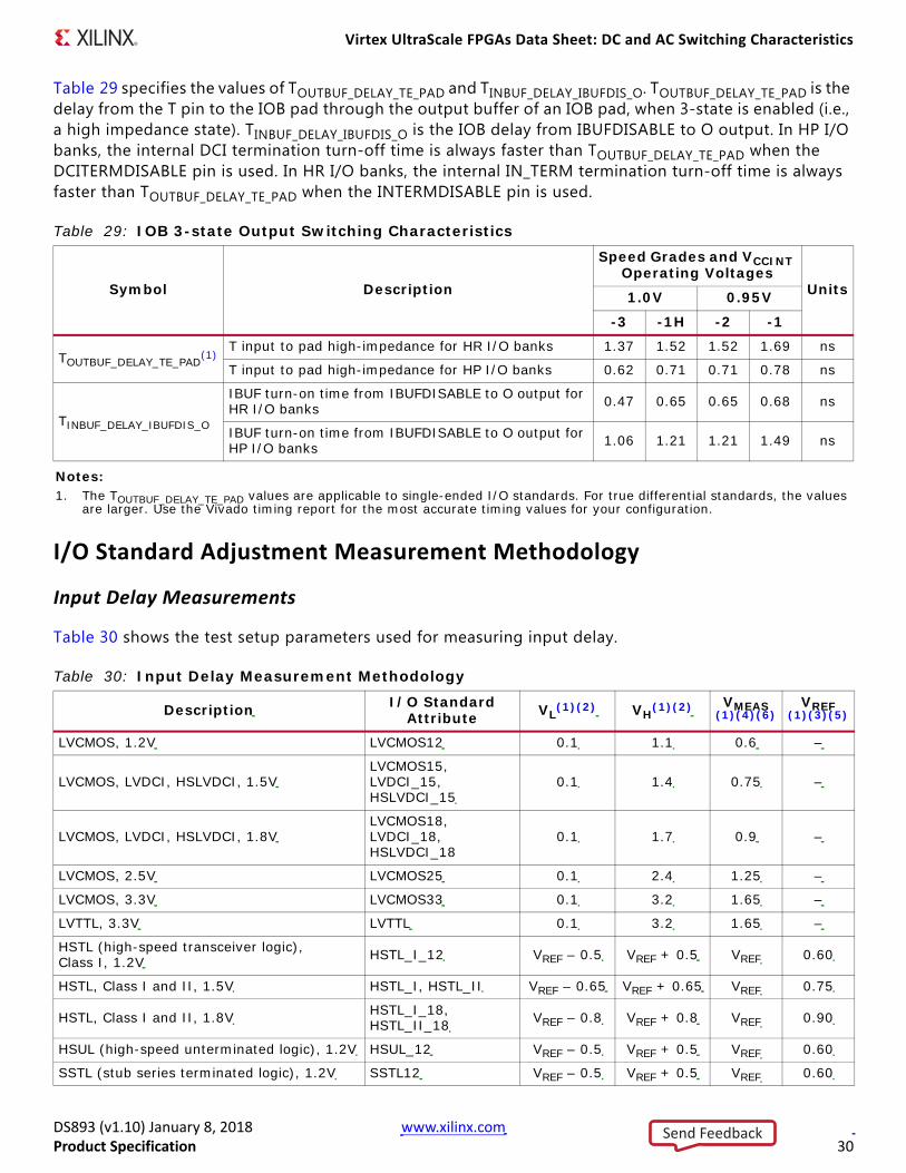
Table 29 specifies the values of TOUTBUF_DELAY_TE_PAD and TINBUF_DELAY_IBUFDIS_O. TOUTBUF_DELAY_TE_PAD is the delay from the T pin to the IOB pad through the output buffer of an IOB pad, when 3-state is enabled (i.e., a high impedance state). TINBUF_DELAY_IBUFDIS_O is the IOB delay from IBUFDISABLE to O output. In HP I/O banks, the internal DCI termination turn-off time is always faster than TOUTBUF_DELAY_TE_PAD when the DCITERMDISABLE pin is used. In HR I/O banks, the internal IN_TERM termination turn-off time is always faster than TOUTBUF_DELAY_TE_PAD when the INTERMDISABLE pin is used.
I/O Standard Adjustment Measurement Methodology
Input Delay Measurements
Table 30 shows the test setup parameters used for measuring input delay.
Table 29: IOB 3-state Output Switching Characteristics
Symbol Description
Speed Grades and VCCINT Operating Voltages
Units1.0V 0.95V
-3 -1H -2 -1
TOUTBUF_DELAY_TE_PAD(1)
T input to pad high-impedance for HR I/O banks 1.37 1.52 1.52 1.69 ns
T input to pad high-impedance for HP I/O banks 0.62 0.71 0.71 0.78 ns
TINBUF_DELAY_IBUFDIS_O
IBUF turn-on time from IBUFDISABLE to O output for HR I/O banks 0.47 0.65 0.65 0.68 ns
IBUF turn-on time from IBUFDISABLE to O output for HP I/O banks 1.06 1.21 1.21 1.49 ns
Notes: 1. The TOUTBUF_DELAY_TE_PAD values are applicable to single-ended I/O standards. For true differential standards, the values
are larger. Use the Vivado timing report for the most accurate timing values for your configuration.
Table 30: Input Delay Measurement Methodology
Description I/O Standard Attribute VL
(1)(2) VH(1)(2) VMEAS
(1)(4)(6)VREF
(1)(3)(5)
LVCMOS, 1.2V LVCMOS12 0.1 1.1 0.6 –
LVCMOS, LVDCI, HSLVDCI, 1.5VLVCMOS15, LVDCI_15, HSLVDCI_15
0.1 1.4 0.75 –
LVCMOS, LVDCI, HSLVDCI, 1.8VLVCMOS18, LVDCI_18, HSLVDCI_18
0.1 1.7 0.9 –
LVCMOS, 2.5V LVCMOS25 0.1 2.4 1.25 –
LVCMOS, 3.3V LVCMOS33 0.1 3.2 1.65 –
LVTTL, 3.3V LVTTL 0.1 3.2 1.65 –
HSTL (high-speed transceiver logic), Class I, 1.2V HSTL_I_12 VREF – 0.5 VREF + 0.5 VREF 0.60
HSTL, Class I and II, 1.5V HSTL_I, HSTL_II VREF – 0.65 VREF + 0.65 VREF 0.75
HSTL, Class I and II, 1.8V HSTL_I_18, HSTL_II_18 VREF – 0.8 VREF + 0.8 VREF 0.90
HSUL (high-speed unterminated logic), 1.2V HSUL_12 VREF – 0.5 VREF + 0.5 VREF 0.60
SSTL (stub series terminated logic), 1.2V SSTL12 VREF – 0.5 VREF + 0.5 VREF 0.60
Send Feedback

Virtex UltraScale FPGAs Data Sheet: DC and AC Switching Characteristics
DS893 (v1.10) January 8, 2018 www.xilinx.comProduct Specification 31
SSTL, 1.35V SSTL135, SSTL135_R VREF – 0.575 VREF + 0.575 VREF 0.675
SSTL, 1.5V SSTL15, SSTL15_R VREF – 0.65 VREF + 0.65 VREF 0.75
SSTL, Class I and II, 1.8V SSTL18_I, SSTL18_II VREF – 0.8 VREF + 0.8 VREF 0.90
POD10, 1.0V POD10 VREF – 0.6 VREF + 0.6 VREF 0.70
POD12, 1.2V POD12 VREF – 0.74 VREF + 0.74 VREF 0.84
DIFF_HSTL, Class I, 1.2V DIFF_HSTL_I_12 0.6 – 0.125 0.6 + 0.125 0(6) –
DIFF_HSTL, Class I and II,1.5V DIFF_HSTL_I, DIFF_HSTL_II 0.75 – 0.125 0.75 + 0.125 0(6) –
DIFF_HSTL, Class I and II, 1.8V DIFF_HSTL_I_18, DIFF_HSTL_II_18 0.9 – 0.125 0.9 + 0.125 0(6) –
DIFF_HSUL, 1.2V DIFF_HSUL_12 0.6 – 0.125 0.6 + 0.125 0(6) –
DIFF_SSTL, 1.2V DIFF_SSTL12 0.6 – 0.125 0.6 + 0.125 0(6) –
DIFF_SSTL135/DIFF_SSTL135_R, 1.35V DIFF_SSTL135, DIFF_SSTL135_R
0.675 – 0.125
0.675 + 0.125 0(6) –
DIFF_SSTL15/DIFF_SSTL15_R, 1.5V DIFF_SSTL15, DIFF_SSTL15_R 0.75 – 0.125 0.75 + 0.125 0(6) –
DIFF_SSTL18_I/DIFF_SSTL18_II, 1.8V DIFF_SSTL18_I, DIFF_SSTL18_II 0.9 – 0.125 0.9 + 0.125 0(6) –
DIFF_POD10, 1.0V DIFF_POD10 0.70 – 0.125 0.70 + 0.125 0(6) –
DIFF_POD12, 1.2V DIFF_POD12 0.84 – 0.125 0.84 + 0.125 0(6) –
LVDS (low-voltage differential signaling), 1.8V LVDS 0.9 – 0.125 0.9 + 0.125 0(6) –
LVDS_25, 2.5V LVDS_25 1.25 – 0.125 1.25 + 0.125 0(6) –
SUB_LVDS, 1.8V SUB_LVDS 0.9 – 0.125 0.9 + 0.125 0(6) –
SLVS, 1.8V SLVS_400_18 0.9 – 0.125 0.9 + 0.125 0(6) –
SLVS, 2.5V SLVS_400_25 1.25 – 0.125 1.25 + 0.125 0(6) –
LVPECL, 2.5 LVPECL 1.25 – 0.125 1.25 + 0.125 0(6) –
BLVDS_25, 2.5V BLVDS_25 1.25 – 0.125 1.25 + 0.125 0(6) –
MINI_LVDS_25, 2.5V MINI_LVDS_25 1.25 – 0.125 1.25 + 0.125 0(6) –
PPDS_25 PPDS_25 1.25 – 0.125 1.25 + 0.125 0(6) –
RSDS_25 RSDS_25 1.25 – 0.125 1.25 + 0.125 0(6) –
TMDS_33 TMDS_33 3 – 0.125 3 + 0.125 0(6) –
Notes: 1. The input delay measurement methodology parameters for LVDCI are the same for LVCMOS standards of the same
voltage. Input delay measurement methodology parameters for HSLVDCI are the same as for HSTL_II standards of the same voltage. Parameters for all other DCI standards are the same for the corresponding non-DCI standards.
2. Input waveform switches between VLand VH.3. Measurements are made at typical, minimum, and maximum VREF values. Reported delays reflect worst case of these
measurements. VREF values listed are typical.4. Input voltage level from which measurement starts.5. This is an input voltage reference that bears no relation to the VREF/VMEAS parameters found in IBIS models and/or noted
in Figure 1.6. The value given is the differential input voltage.
Table 30: Input Delay Measurement Methodology (Cont’d)
Description I/O Standard Attribute VL
(1)(2) VH(1)(2) VMEAS
(1)(4)(6)VREF
(1)(3)(5)
Send Feedback
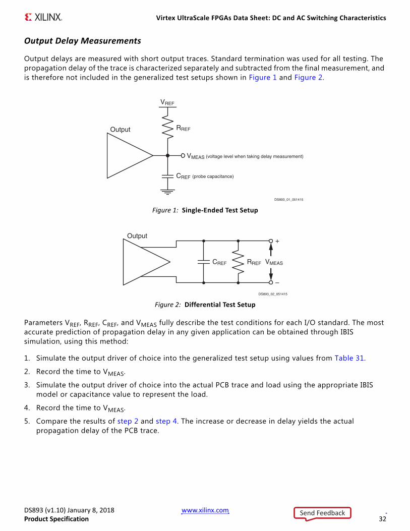
Virtex UltraScale FPGAs Data Sheet: DC and AC Switching Characteristics
DS893 (v1.10) January 8, 2018 www.xilinx.comProduct Specification 32
Output Delay Measurements
Output delays are measured with short output traces. Standard termination was used for all testing. The propagation delay of the trace is characterized separately and subtracted from the final measurement, and is therefore not included in the generalized test setups shown in Figure 1 and Figure 2.
Parameters VREF, RREF, CREF, and VMEAS fully describe the test conditions for each I/O standard. The most accurate prediction of propagation delay in any given application can be obtained through IBIS simulation, using this method:
1. Simulate the output driver of choice into the generalized test setup using values from Table 31.
2. Record the time to VMEAS.
3. Simulate the output driver of choice into the actual PCB trace and load using the appropriate IBIS model or capacitance value to represent the load.
4. Record the time to VMEAS.
5. Compare the results of step 2 and step 4. The increase or decrease in delay yields the actual propagation delay of the PCB trace.
X-Ref Target - Figure 1
Figure 1: Single-Ended Test Setup
X-Ref Target - Figure 2
Figure 2: Differential Test Setup
VREF
RREF
VMEAS (voltage level when taking delay measurement)
CREF (probe capacitance)
Output
DS893_01_051415
RREF VMEAS
+
–
CREF
Output
DS893_02_051415
Send Feedback

Virtex UltraScale FPGAs Data Sheet: DC and AC Switching Characteristics
DS893 (v1.10) January 8, 2018 www.xilinx.comProduct Specification 33
Table 31: Output Delay Measurement Methodology
Description I/O Standard Attribute RREF(Ω)
CREF(1)
(pF)VMEAS
(V)VREF(V)
LVCMOS, 1.2V LVCMOS12 1M 0 0.6 0
LVCMOS 1.5V LVCMOS15 1M 0 0.75 0
LVCMOS 1.8V LVCMOS18 1M 0 0.9 0
LVCMOS, 2.5V LVCMOS25 1M 0 1.25 0
LVCMOS, 3.3V LVCMOS33 1M 0 1.65 0
LVTTL, 3.3V LVTTL 1M 0 1.65 0
LVDCI/HSLVDCI, 1.5V LVDCI_15, HSLVDCI_15 50 0 VREF 0.75
LVDCI/HSLVDCI, 1.8V LVDCI_18, HSLVDCI_18 50 0 VREF 0.9
HSTL (high-speed transceiver logic), Class I, 1.2V HSTL_I_12 50 0 VREF 0.6
HSTL, Class I, 1.5V HSTL_I 50 0 VREF 0.75
HSTL, Class II, 1.5V HSTL_II 25 0 VREF 0.75
HSTL, Class I, 1.8V HSTL_I_18 50 0 VREF 0.9
HSTL, Class II, 1.8V HSTL_II_18 25 0 VREF 0.9
HSUL (high-speed unterminated logic), Class I, 1.2V HSUL_12 50 0 VREF 0.6
SSTL12, 1.2V SSTL12 50 0 VREF 0.6
SSTL135/SSTL135_R, 1.35V SSTL135, SSTL135_R 50 0 VREF 0.675
SSTL15/SSTL15_R, 1.5V SSTL15, SSTL15_R 50 0 VREF 0.75
SSTL (stub series terminated logic), Class I and Class II, 1.8V SSTL18_I, SSTL18_II 50 0 VREF 0.9
POD10, 1.0V POD10 50 0 VREF 1.0
POD12, 1.2V POD12 50 0 VREF 1.2
DIFF_HSTL, Class I, 1.2V DIFF_HSTL_I_12 50 0 VREF 0.6
DIFF_HSTL, Class I and II, 1.5V DIFF_HSTL_I, DIFF_HSTL_II 50 0 VREF 0.75
DIFF_HSTL, Class I and II, 1.8V DIFF_HSTL_I_18, DIFF_HSTL_II_18 50 0 VREF 0.9
DIFF_HSUL_12, 1.2V DIFF_HSUL_12 50 0 VREF 0.6
DIFF_SSTL12, 1.2V DIFF_SSTL12 50 0 VREF 0.6
DIFF_SSTL135/DIFF_SSTL135_R, 1.35V DIFF_SSTL135, DIFF_SSTL135_R 50 0 VREF 0.675
DIFF_SSTL15/DIFF_SSTL15_R, 1.5V DIFF_SSTL15, DIFF_SSTL15_R 50 0 VREF 0.75
DIFF_SSTL18, Class I and II, 1.8V DIFF_SSTL18_I, DIFF_SSTL18_II 50 0 VREF 0.9
DIFF_POD10, 1.0V DIFF_POD10 50 0 VREF 1.0
DIFF_POD12, 1.2V DIFF_POD12 50 0 VREF 1.2
LVDS (low-voltage differential signaling), 1.8V LVDS 100 0 0(2) 0
LVDS, 2.5V LVDS_25 100 0 0(2) 0
BLVDS (Bus LVDS), 2.5V BLVDS_25 100 0 0(2) 0
Mini LVDS, 2.5V MINI_LVDS_25 100 0 0(2) 0
PPDS_25 PPDS_25 100 0 0(2) 0
RSDS_25 RSDS_25 100 0 0(2) 0
Send Feedback
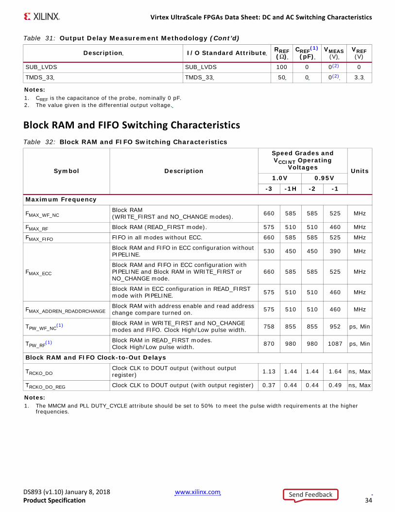
Virtex UltraScale FPGAs Data Sheet: DC and AC Switching Characteristics
DS893 (v1.10) January 8, 2018 www.xilinx.comProduct Specification 34
Block RAM and FIFO Switching Characteristics
SUB_LVDS SUB_LVDS 100 0 0(2) 0
TMDS_33 TMDS_33 50 0 0(2) 3.3
Notes: 1. CREF is the capacitance of the probe, nominally 0 pF.2. The value given is the differential output voltage.
Table 32: Block RAM and FIFO Switching Characteristics
Symbol Description
Speed Grades and VCCINT Operating
Voltages Units1.0V 0.95V
-3 -1H -2 -1
Maximum Frequency
FMAX_WF_NCBlock RAM (WRITE_FIRST and NO_CHANGE modes). 660 585 585 525 MHz
FMAX_RF Block RAM (READ_FIRST mode). 575 510 510 460 MHz
FMAX_FIFO FIFO in all modes without ECC. 660 585 585 525 MHz
FMAX_ECC
Block RAM and FIFO in ECC configuration without PIPELINE. 530 450 450 390 MHz
Block RAM and FIFO in ECC configuration with PIPELINE and Block RAM in WRITE_FIRST or NO_CHANGE mode.
660 585 585 525 MHz
Block RAM in ECC configuration in READ_FIRST mode with PIPELINE. 575 510 510 460 MHz
FMAX_ADDREN_RDADDRCHANGEBlock RAM with address enable and read address change compare turned on. 575 510 510 460 MHz
TPW_WF_NC(1) Block RAM in WRITE_FIRST and NO_CHANGE
modes and FIFO. Clock High/Low pulse width. 758 855 855 952 ps, Min
TPW_RF(1) Block RAM in READ_FIRST modes.
Clock High/Low pulse width. 870 980 980 1087 ps, Min
Block RAM and FIFO Clock-to-Out Delays
TRCKO_DOClock CLK to DOUT output (without output register) 1.13 1.44 1.44 1.64 ns, Max
TRCKO_DO_REG Clock CLK to DOUT output (with output register) 0.37 0.44 0.44 0.49 ns, Max
Notes: 1. The MMCM and PLL DUTY_CYCLE attribute should be set to 50% to meet the pulse width requirements at the higher
frequencies.
Table 31: Output Delay Measurement Methodology (Cont’d)
Description I/O Standard Attribute RREF(Ω)
CREF(1)
(pF)VMEAS
(V)VREF(V)
Send Feedback
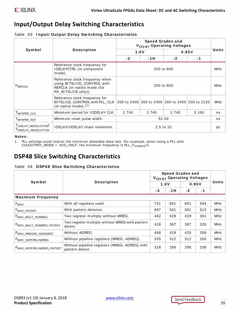
Virtex UltraScale FPGAs Data Sheet: DC and AC Switching Characteristics
DS893 (v1.10) January 8, 2018 www.xilinx.comProduct Specification 35
Input/Output Delay Switching Characteristics
DSP48 Slice Switching Characteristics
Table 33: Input/Output Delay Switching Characteristics
Symbol Description
Speed Grades and VCCINT Operating Voltages
Units1.0V 0.95V
-3 -1H -2 -1
FREFCLK
Reference clock frequency for IDELAYCTRL (in component mode).
200 to 800 MHz
Reference clock frequency when using BITSLICE_CONTROL with REFCLK (in native mode (for RX_BITSLICE only)).
200 to 800 MHz
Reference clock frequency for BITSLICE_CONTROL with PLL_CLK (in native mode).(1)
200 to 2400 200 to 2400 200 to 2400 200 to 2133 MHz
TMINPER_CLK Minimum period for IODELAY CLK. 2.740 2.740 2.740 3.160 ns
TMINPER_RST Minimum reset pulse width. 52.00 ns
TIDELAY_RESOLUTION/TODELAY_RESOLUTION
IDELAY/ODELAY chain resolution. 2.5 to 15 ps
Notes: 1. PLL settings could restrict the minimum allowable data rate. For example, when using a PLL with
CLKOUTPHY_MODE = VCO_HALF, the minimum frequency is PLL_FVCOMIN/2.
Table 34: DSP48 Slice Switching Characteristics
Symbol Description
Speed Grades and VCCINT Operating Voltages
Units1.0V 0.95V
-3 -1H -2 -1
Maximum FrequencyFMAX With all registers used. 741 661 661 594 MHz
FMAX_PATDET With pattern detector. 687 581 581 512 MHz
FMAX_MULT_NOMREG Two register multiply without MREG. 462 429 429 361 MHz
FMAX_MULT_NOMREG_PATDETTwo register multiply without MREG with pattern detect. 428 387 387 326 MHz
FMAX_PREADD_NOADREG Without ADREG. 468 429 429 358 MHz
FMAX_NOPIPELINEREG Without pipeline registers (MREG, ADREG). 335 312 312 260 MHz
FMAX_NOPIPELINEREG_PATDETWithout pipeline registers (MREG, ADREG) with pattern detect. 316 286 286 238 MHz
Send Feedback
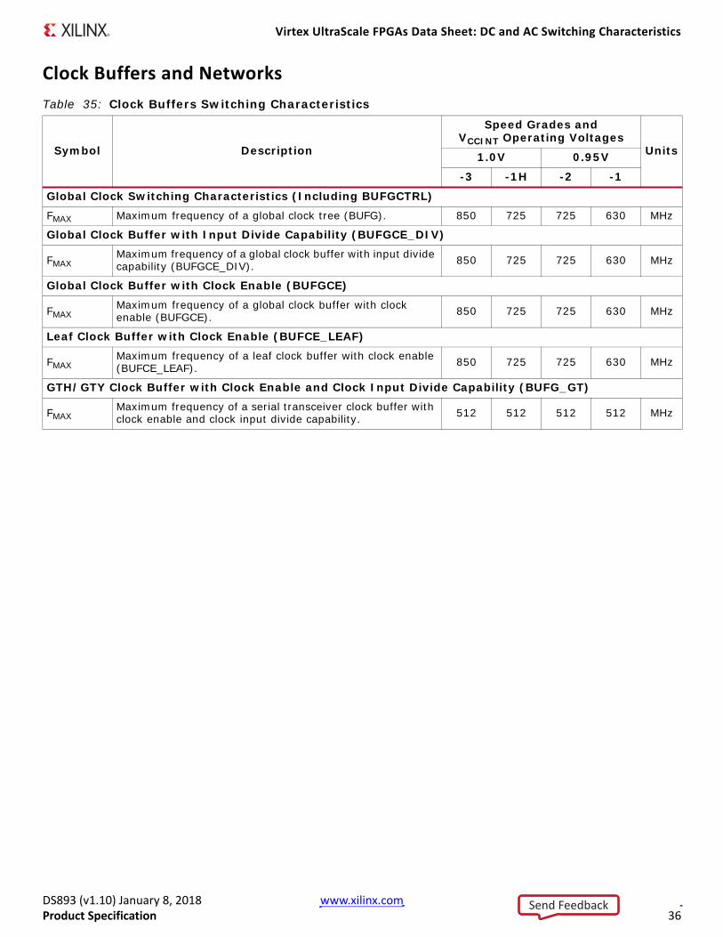
Virtex UltraScale FPGAs Data Sheet: DC and AC Switching Characteristics
DS893 (v1.10) January 8, 2018 www.xilinx.comProduct Specification 36
Clock Buffers and NetworksTable 35: Clock Buffers Switching Characteristics
Symbol Description
Speed Grades and VCCINT Operating Voltages
Units1.0V 0.95V
-3 -1H -2 -1
Global Clock Switching Characteristics (Including BUFGCTRL)FMAX Maximum frequency of a global clock tree (BUFG). 850 725 725 630 MHz
Global Clock Buffer with Input Divide Capability (BUFGCE_DIV)
FMAXMaximum frequency of a global clock buffer with input divide capability (BUFGCE_DIV). 850 725 725 630 MHz
Global Clock Buffer with Clock Enable (BUFGCE)
FMAXMaximum frequency of a global clock buffer with clock enable (BUFGCE). 850 725 725 630 MHz
Leaf Clock Buffer with Clock Enable (BUFCE_LEAF)
FMAXMaximum frequency of a leaf clock buffer with clock enable (BUFCE_LEAF). 850 725 725 630 MHz
GTH/GTY Clock Buffer with Clock Enable and Clock Input Divide Capability (BUFG_GT)
FMAXMaximum frequency of a serial transceiver clock buffer with clock enable and clock input divide capability. 512 512 512 512 MHz
Send Feedback
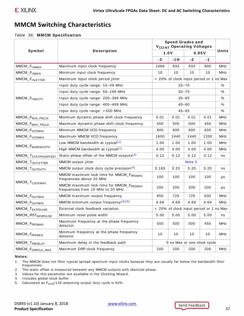
Virtex UltraScale FPGAs Data Sheet: DC and AC Switching Characteristics
DS893 (v1.10) January 8, 2018 www.xilinx.comProduct Specification 37
MMCM Switching CharacteristicsTable 36: MMCM Specification
Symbol Description
Speed Grades and VCCINT Operating Voltages
Units1.0V 0.95V
-3 -1H -2 -1MMCM_FINMAX Maximum input clock frequency 1066 933 933 800 MHz
MMCM_FINMIN Minimum input clock frequency 10 10 10 10 MHz
MMCM_FINJITTER Maximum input clock period jitter < 20% of clock input period or 1 ns Max
MMCM_FINDUTY
Input duty cycle range: 10–49 MHz 25–75 %
Input duty cycle range: 50–199 MHz 30–70 %
Input duty cycle range: 200–399 MHz 35–65 %
Input duty cycle range: 400–499 MHz 40–60 %
Input duty cycle range: >500 MHz 45–55 %
MMCM_FMIN_PSCLK Minimum dynamic phase shift clock frequency 0.01 0.01 0.01 0.01 MHz
MMCM_FMAX_PSCLK Maximum dynamic phase shift clock frequency 550 500 500 450 MHz
MMCM_FVCOMIN Minimum MMCM VCO frequency 600 600 600 600 MHz
MMCM_FVCOMAX Maximum MMCM VCO frequency 1600 1440 1440 1200 MHz
MMCM_FBANDWIDTHLow MMCM bandwidth at typical(1) 1.00 1.00 1.00 1.00 MHz
High MMCM bandwidth at typical(1) 4.00 4.00 4.00 4.00 MHz
MMCM_TSTATPHAOFFSET Static phase offset of the MMCM outputs(2) 0.12 0.12 0.12 0.12 ns
MMCM_TOUTJITTER MMCM output jitter Note 3
MMCM_TOUTDUTY MMCM output clock duty cycle precision(4) 0.165 0.20 0.20 0.20 ns
MMCM_TLOCKMAX
MMCM maximum lock time for MMCM_FPFDMIN frequencies above 20 MHz 100 100 100 100 µs
MMCM maximum lock time for MMCM_FPFDMIN frequencies from 10 MHz to 20 MHz 200 200 200 200 µs
MMCM_FOUTMAX MMCM maximum output frequency 850 725 725 630 MHz
MMCM_FOUTMIN MMCM minimum output frequency(4)(5) 4.69 4.69 4.69 4.69 MHz
MMCM_TEXTFDVAR External clock feedback variation < 20% of clock input period or 1 ns Max
MMCM_RSTMINPULSE Minimum reset pulse width 5.00 5.00 5.00 5.00 ns
MMCM_FPFDMAXMaximum frequency at the phase frequency detector 550 500 500 450 MHz
MMCM_FPFDMINMinimum frequency at the phase frequency detector 10 10 10 10 MHz
MMCM_TFBDELAY Maximum delay in the feedback path 5 ns Max or one clock cycle
MMCM_FDRPCLK_MAX Maximum DRP clock frequency 200 200 200 200 MHz
Notes: 1. The MMCM does not filter typical spread-spectrum input clocks because they are usually far below the bandwidth filter
frequencies.2. The static offset is measured between any MMCM outputs with identical phase.3. Values for this parameter are available in the Clocking Wizard.4. Includes global clock buffer.5. Calculated as FVCO/128 assuming output duty cycle is 50%.
Send Feedback
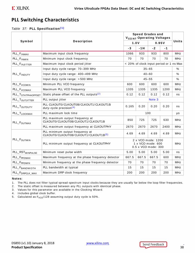
Virtex UltraScale FPGAs Data Sheet: DC and AC Switching Characteristics
DS893 (v1.10) January 8, 2018 www.xilinx.comProduct Specification 38
PLL Switching CharacteristicsTable 37: PLL Specification(1)
Symbol Description
Speed Grades and VCCINT Operating Voltages
Units1.0V 0.95V
-3 -1H -2 -1PLL_FINMAX Maximum input clock frequency 1066 933 933 800 MHz
PLL_FINMIN Minimum input clock frequency 70 70 70 70 MHz
PLL_FINJITTER Maximum input clock period jitter < 20% of clock input period or 1 ns Max
PLL_FINDUTY
Input duty cycle range: 70–399 MHz 35–65 %
Input duty cycle range: 400–499 MHz 40–60 %
Input duty cycle range: >500 MHz 45–55 %
PLL_FVCOMIN Minimum PLL VCO frequency 600 600 600 600 MHz
PLL_FVCOMAX Maximum PLL VCO frequency 1335 1335 1335 1200 MHz
PLL_TSTATPHAOFFSET Static phase offset of the PLL outputs(2) 0.12 0.12 0.12 0.12 ns
PLL_TOUTJITTER PLL output jitter Note 3
PLL_TOUTDUTYPLL CLKOUT0/CLKOUT0B/CLKOUT1/CLKOUT1B duty-cycle precision(4) 0.165 0.20 0.20 0.20 ns
PLL_TLOCKMAX PLL maximum lock time 100 µs
PLL_FOUTMAX
PLL maximum output frequency at CLKOUT0/CLKOUT0B/CLKOUT1/CLKOUT1B 850 725 725 630 MHz
PLL maximum output frequency at CLKOUTPHY 2670 2670 2670 2400 MHz
PLL_FOUTMIN
PLL minimum output frequency at CLKOUT0/CLKOUT0B/CLKOUT1/CLKOUT1B(5) 4.69 4.69 4.69 4.69 MHz
PLL minimum output frequency at CLKOUTPHY2 x VCO mode: 12001 x VCO mode: 600
0.5 x VCO mode: 300MHz
PLL_RSTMINPULSE Minimum reset pulse width 5.00 5.00 5.00 5.00 ns
PLL_FPFDMAX Maximum frequency at the phase frequency detector 667.5 667.5 667.5 600 MHz
PLL_FPFDMIN Minimum frequency at the phase frequency detector 70 70 70 70 MHz
PLL_FBANDWIDTH PLL bandwidth at typical 15 15 15 15 MHz
PLL_FDRPCLK_MAX Maximum DRP clock frequency 200 200 200 200 MHz
Notes: 1. The PLL does not filter typical spread-spectrum input clocks because they are usually far below the loop filter frequencies.2. The static offset is measured between any PLL outputs with identical phase.3. Values for this parameter are available in the Clocking Wizard. 4. Includes global clock buffer.5. Calculated as FVCO/128 assuming output duty cycle is 50%.
Send Feedback
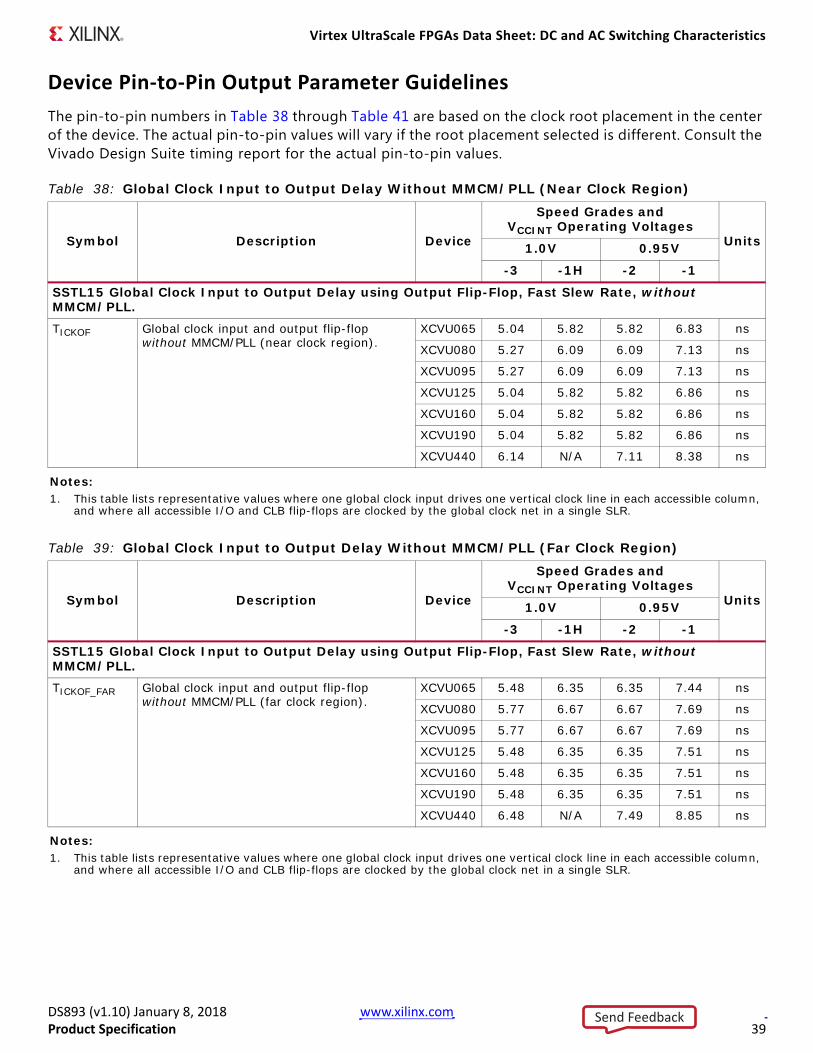
Virtex UltraScale FPGAs Data Sheet: DC and AC Switching Characteristics
DS893 (v1.10) January 8, 2018 www.xilinx.comProduct Specification 39
Device Pin-to-Pin Output Parameter GuidelinesThe pin-to-pin numbers in Table 38 through Table 41 are based on the clock root placement in the center of the device. The actual pin-to-pin values will vary if the root placement selected is different. Consult the Vivado Design Suite timing report for the actual pin-to-pin values.
Table 38: Global Clock Input to Output Delay Without MMCM/PLL (Near Clock Region)
Symbol Description Device
Speed Grades and VCCINT Operating Voltages
Units1.0V 0.95V
-3 -1H -2 -1
SSTL15 Global Clock Input to Output Delay using Output Flip-Flop, Fast Slew Rate, without MMCM/PLL.TICKOF Global clock input and output flip-flop
without MMCM/PLL (near clock region).XCVU065 5.04 5.82 5.82 6.83 ns
XCVU080 5.27 6.09 6.09 7.13 ns
XCVU095 5.27 6.09 6.09 7.13 ns
XCVU125 5.04 5.82 5.82 6.86 ns
XCVU160 5.04 5.82 5.82 6.86 ns
XCVU190 5.04 5.82 5.82 6.86 ns
XCVU440 6.14 N/A 7.11 8.38 ns
Notes: 1. This table lists representative values where one global clock input drives one vertical clock line in each accessible column,
and where all accessible I/O and CLB flip-flops are clocked by the global clock net in a single SLR.
Table 39: Global Clock Input to Output Delay Without MMCM/PLL (Far Clock Region)
Symbol Description Device
Speed Grades and VCCINT Operating Voltages
Units1.0V 0.95V
-3 -1H -2 -1
SSTL15 Global Clock Input to Output Delay using Output Flip-Flop, Fast Slew Rate, without MMCM/PLL.TICKOF_FAR Global clock input and output flip-flop
without MMCM/PLL (far clock region).XCVU065 5.48 6.35 6.35 7.44 ns
XCVU080 5.77 6.67 6.67 7.69 ns
XCVU095 5.77 6.67 6.67 7.69 ns
XCVU125 5.48 6.35 6.35 7.51 ns
XCVU160 5.48 6.35 6.35 7.51 ns
XCVU190 5.48 6.35 6.35 7.51 ns
XCVU440 6.48 N/A 7.49 8.85 ns
Notes: 1. This table lists representative values where one global clock input drives one vertical clock line in each accessible column,
and where all accessible I/O and CLB flip-flops are clocked by the global clock net in a single SLR.
Send Feedback

Virtex UltraScale FPGAs Data Sheet: DC and AC Switching Characteristics
DS893 (v1.10) January 8, 2018 www.xilinx.comProduct Specification 40
Table 40: Global Clock Input to Output Delay With MMCM
Symbol Description Device
Speed Grades and VCCINT Operating Voltages
Units1.0V 0.95V
-3 -1H -2 -1
SSTL15 Global Clock Input to Output Delay using Output Flip-Flop, Fast Slew Rate, with MMCM.TICKOFMMCMCC Global clock input and output flip-flop with
MMCM.XCVU065 1.36 1.61 1.61 1.93 ns
XCVU080 1.36 1.59 1.59 1.85 ns
XCVU095 1.36 1.59 1.59 1.85 ns
XCVU125 1.36 1.61 1.61 1.94 ns
XCVU160 1.36 1.61 1.61 1.94 ns
XCVU190 1.36 1.61 1.61 1.94 ns
XCVU440 1.37 N/A 1.62 1.88 ns
Notes: 1. This table lists representative values where one global clock input drives one vertical clock line in each accessible column,
and where all accessible I/O and CLB flip-flops are clocked by the global clock net in a single SLR.2. MMCM output jitter is already included in the timing calculation.
Table 41: Global Clock Input to Output Delay With PLL
Symbol Description Device
Speed Grades and VCCINT Operating Voltages
Units1.0V 0.95V
-3 -1H -2 -1
SSTL15 Global Clock Input to Output Delay using Output Flip-Flop, Fast Slew Rate, with PLL.TICKOF_PLL_CC Global clock input and output flip-flop with
PLL.XCVU065 4.70 5.38 5.38 6.23 ns
XCVU080 4.99 5.70 5.70 6.49 ns
XCVU095 4.99 5.70 5.70 6.49 ns
XCVU125 4.70 5.38 5.38 6.31 ns
XCVU160 4.70 5.38 5.38 6.31 ns
XCVU190 4.70 5.38 5.38 6.31 ns
XCVU440 5.70 N/A 6.53 7.65 ns
Notes: 1. This table lists representative values where one global clock input drives one vertical clock line in each accessible column,
and where all accessible I/O and CLB flip-flops are clocked by the global clock net in a single SLR.2. PLL output jitter is already included in the timing calculation.
Send Feedback

Virtex UltraScale FPGAs Data Sheet: DC and AC Switching Characteristics
DS893 (v1.10) January 8, 2018 www.xilinx.comProduct Specification 41
Device Pin-to-Pin Input Parameter GuidelinesThe pin-to-pin numbers in Table 42 and Table 43 are based on the clock root placement in the center of the device. The actual pin-to-pin values will vary if the root placement selected is different. Consult the Vivado Design Suite timing report for the actual pin-to-pin values.
Table 42: Global Clock Input Setup and Hold With MMCM
Symbol Description Device
Speed Grades and VCCINT Operating Voltages
Units1.0V 0.95V
-3 -1H -2 -1
Input Setup and Hold Time Relative to Global Clock Input Signal using SSTL15 Standard.(1)(2)(3)
TPSMMCMCC_VU065 Global clock input and input flip-flop (or latch) with MMCM.
SetupXCVU065
2.36 2.48 2.38 2.67 ns
TPHMMCMCC_VU065 Hold –0.25 –0.25 –0.25 –0.25 ns
TPSMMCMCC_VU080 SetupXCVU080
2.22 2.45 2.25 2.55 ns
TPHMMCMCC_VU080 Hold –0.47 –0.47 –0.47 –0.47 ns
TPSMMCMCC_VU095 SetupXCVU095
2.22 2.45 2.25 2.55 ns
TPHMMCMCC_VU095 Hold –0.47 –0.47 –0.47 –0.47 ns
TPSMMCMCC_VU125 SetupXCVU125
2.21 2.48 2.23 2.66 ns
TPHMMCMCC_VU125 Hold –0.13 –0.13 –0.13 –0.13 ns
TPSMMCMCC_VU160 SetupXCVU160
2.21 2.48 2.23 2.66 ns
TPHMMCMCC_VU160 Hold –0.12 –0.12 –0.12 –0.12 ns
TPSMMCMCC_VU190 SetupXCVU190
2.21 2.48 2.23 2.66 ns
TPHMMCMCC_VU190 Hold –0.13 –0.13 –0.13 –0.13 ns
TPSMMCMCC_VU440 SetupXCVU440
2.31 N/A 2.32 2.86 ns
TPHMMCMCC_VU440 Hold –0.07 N/A –0.07 –0.07 ns
Notes: 1. Setup and hold times are measured over worst case conditions (process, voltage, temperature). Setup time is measured
relative to the global clock input signal using the slowest process, slowest temperature, and slowest voltage. Hold time is measured relative to the global clock input signal using the fastest process, fastest temperature, and fastest voltage.
2. This table lists representative values where one global clock input drives one vertical clock line in each accessible column, and where all accessible I/O and CLB flip-flops are clocked by the global clock net in a single SLR.
3. Use IBIS to determine any duty-cycle distortion incurred using various standards.
Send Feedback
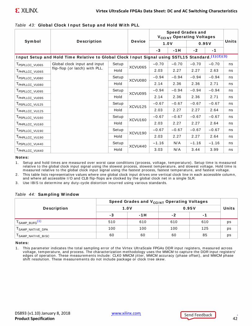
Virtex UltraScale FPGAs Data Sheet: DC and AC Switching Characteristics
DS893 (v1.10) January 8, 2018 www.xilinx.comProduct Specification 42
Table 43: Global Clock Input Setup and Hold With PLL
Symbol Description Device
Speed Grades and VCCINT Operating Voltages
Units1.0V 0.95V
-3 -1H -2 -1
Input Setup and Hold Time Relative to Global Clock Input Signal using SSTL15 Standard.(1)(2)(3)
TPSPLLCC_VU065 Global clock input and input flip-flop (or latch) with PLL.
SetupXCVU065
–0.70 –0.70 –0.70 –0.70 ns
TPHPLLCC_VU065 Hold 2.03 2.27 2.27 2.63 ns
TPSPLLCC_VU080 SetupXCVU080
–0.94 –0.94 –0.94 –0.94 ns
TPHPLLCC_VU080 Hold 2.14 2.36 2.36 2.71 ns
TPSPLLCC_VU095 SetupXCVU095
–0.94 –0.94 –0.94 –0.94 ns
TPHPLLCC_VU095 Hold 2.14 2.36 2.36 2.71 ns
TPSPLLCC_VU125 SetupXCVU125
–0.67 –0.67 –0.67 –0.67 ns
TPHPLLCC_VU125 Hold 2.03 2.27 2.27 2.64 ns
TPSPLLCC_VU160 SetupXCVU160
–0.67 –0.67 –0.67 –0.67 ns
TPHPLLCC_VU160 Hold 2.03 2.27 2.27 2.64 ns
TPSPLLCC_VU190 SetupXCVU190
–0.67 –0.67 –0.67 –0.67 ns
TPHPLLCC_VU190 Hold 2.03 2.27 2.27 2.64 ns
TPSPLLCC_VU440 SetupXCVU440
–1.16 N/A –1.16 –1.16 ns
TPHPLLCC_VU440 Hold 3.03 N/A 3.44 3.99 ns
Notes: 1. Setup and hold times are measured over worst case conditions (process, voltage, temperature). Setup time is measured
relative to the global clock input signal using the slowest process, slowest temperature, and slowest voltage. Hold time is measured relative to the global clock input signal using the fastest process, fastest temperature, and fastest voltage.
2. This table lists representative values where one global clock input drives one vertical clock line in each accessible column, and where all accessible I/O and CLB flip-flops are clocked by the global clock net in a single SLR.
3. Use IBIS to determine any duty-cycle distortion incurred using various standards.
Table 44: Sampling Window
Description
Speed Grades and VCCINT Operating Voltages
Units1.0V 0.95V
-3 -1H -2 -1TSAMP_BUFG
(1) 510 610 610 610 ps
TSAMP_NATIVE_DPA 100 100 100 125 ps
TSAMP_NATIVE_BISC 60 60 60 85 ps
Notes: 1. This parameter indicates the total sampling error of the Virtex UltraScale FPGAs DDR input registers, measured across
voltage, temperature, and process. The characterization methodology uses the MMCM to capture the DDR input registers’ edges of operation. These measurements include: CLK0 MMCM jitter, MMCM accuracy (phase offset), and MMCM phase shift resolution. These measurements do not include package or clock tree skew.
Send Feedback
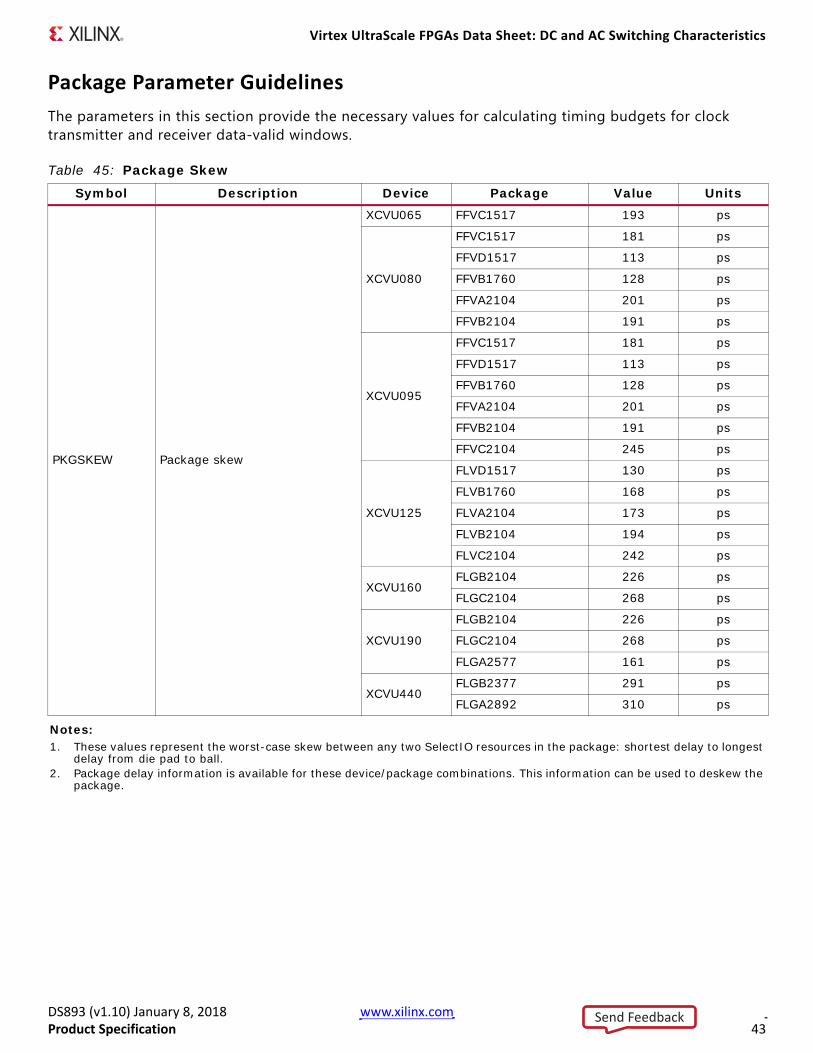
Virtex UltraScale FPGAs Data Sheet: DC and AC Switching Characteristics
DS893 (v1.10) January 8, 2018 www.xilinx.comProduct Specification 43
Package Parameter GuidelinesThe parameters in this section provide the necessary values for calculating timing budgets for clock transmitter and receiver data-valid windows.
Table 45: Package Skew
Symbol Description Device Package Value Units
PKGSKEW Package skew
XCVU065 FFVC1517 193 ps
XCVU080
FFVC1517 181 ps
FFVD1517 113 ps
FFVB1760 128 ps
FFVA2104 201 ps
FFVB2104 191 ps
XCVU095
FFVC1517 181 ps
FFVD1517 113 ps
FFVB1760 128 ps
FFVA2104 201 ps
FFVB2104 191 ps
FFVC2104 245 ps
XCVU125
FLVD1517 130 ps
FLVB1760 168 ps
FLVA2104 173 ps
FLVB2104 194 ps
FLVC2104 242 ps
XCVU160FLGB2104 226 ps
FLGC2104 268 ps
XCVU190
FLGB2104 226 ps
FLGC2104 268 ps
FLGA2577 161 ps
XCVU440FLGB2377 291 ps
FLGA2892 310 ps
Notes: 1. These values represent the worst-case skew between any two SelectIO resources in the package: shortest delay to longest
delay from die pad to ball.2. Package delay information is available for these device/package combinations. This information can be used to deskew the
package.
Send Feedback
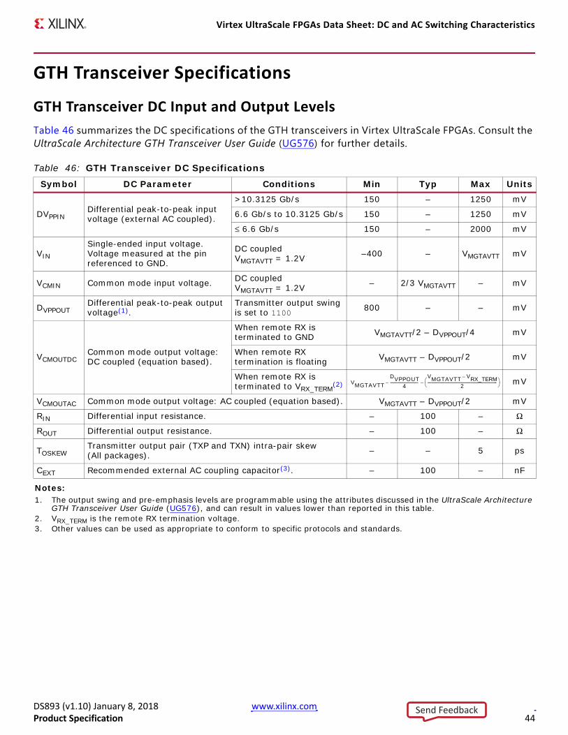
Virtex UltraScale FPGAs Data Sheet: DC and AC Switching Characteristics
DS893 (v1.10) January 8, 2018 www.xilinx.comProduct Specification 44
GTH Transceiver Specifications
GTH Transceiver DC Input and Output LevelsTable 46 summarizes the DC specifications of the GTH transceivers in Virtex UltraScale FPGAs. Consult the UltraScale Architecture GTH Transceiver User Guide (UG576) for further details.
Table 46: GTH Transceiver DC Specifications
Symbol DC Parameter Conditions Min Typ Max Units
DVPPINDifferential peak-to-peak input voltage (external AC coupled).
>10.3125 Gb/s 150 – 1250 mV
6.6 Gb/s to 10.3125 Gb/s 150 – 1250 mV
≤ 6.6 Gb/s 150 – 2000 mV
VIN
Single-ended input voltage. Voltage measured at the pin referenced to GND.
DC coupled VMGTAVTT = 1.2V –400 – VMGTAVTT mV
VCMIN Common mode input voltage. DC coupled VMGTAVTT = 1.2V – 2/3 VMGTAVTT – mV
DVPPOUTDifferential peak-to-peak output voltage(1).
Transmitter output swing is set to 1100 800 – – mV
VCMOUTDCCommon mode output voltage: DC coupled (equation based).
When remote RX is terminated to GND VMGTAVTT/2 – DVPPOUT/4 mV
When remote RX termination is floating VMGTAVTT – DVPPOUT/2 mV
When remote RX is terminated to VRX_TERM
(2) mV
VCMOUTAC Common mode output voltage: AC coupled (equation based). VMGTAVTT – DVPPOUT/2 mV
RIN Differential input resistance. – 100 – Ω
ROUT Differential output resistance. – 100 – Ω
TOSKEWTransmitter output pair (TXP and TXN) intra-pair skew (All packages). – – 5 ps
CEXT Recommended external AC coupling capacitor(3). – 100 – nF
Notes: 1. The output swing and pre-emphasis levels are programmable using the attributes discussed in the UltraScale Architecture
GTH Transceiver User Guide (UG576), and can result in values lower than reported in this table.2. VRX_TERM is the remote RX termination voltage.3. Other values can be used as appropriate to conform to specific protocols and standards.
VMGTAVTTDVPPOUT
4----------------------–
VMGTAVTT VRX_TERM–
2------------------------------------------------------- –
Send Feedback

Virtex UltraScale FPGAs Data Sheet: DC and AC Switching Characteristics
DS893 (v1.10) January 8, 2018 www.xilinx.comProduct Specification 45
Table 47 summarizes the DC specifications of the clock input of the GTH transceivers in Virtex UltraScale FPGAs. Consult the UltraScale Architecture GTH Transceiver User Guide (UG576) for further details.
X-Ref Target - Figure 3
Figure 3: Single-Ended Peak-to-Peak Voltage
X-Ref Target - Figure 4
Figure 4: Differential Peak-to-Peak Voltage
Table 47: GTH Transceiver Clock DC Input Level Specification
Symbol DC Parameter Min Typ Max UnitsVIDIFF Differential peak-to-peak input voltage. 250 – 2000 mV
RIN Differential input resistance. – 100 – Ω
CEXT Required external AC coupling capacitor. – 10 – nF
Table 48: GTH Transceiver Clock Output Level Specification
Symbol Description Conditions Min Typ Max UnitsVOL Output Low voltage for P and N. RT = 100Ω across P and N signals – 400 – mV
VOH Output High voltage for P and N. RT = 100Ω across P and N signals – 760 – mV
VDDOUT
Differential output voltage: (P–N), P = High (N–P), N = High
RT = 100Ω across P and N signals – ±360 – mV
VCMOUT Common mode voltage. RT = 100Ω across P and N signals – 580 – mV
0
+V P
N
ds893_03_120314
Single-EndedPeak-to-Peak Voltage
0
+V
–V P–Nds893_04_120314
Differential peak-to-peak voltage = (Single-ended peak-to-peak voltage) x 2
DifferentialPeak-to-Peak
Voltage
Send Feedback

Virtex UltraScale FPGAs Data Sheet: DC and AC Switching Characteristics
DS893 (v1.10) January 8, 2018 www.xilinx.comProduct Specification 46
GTH Transceiver Switching CharacteristicsConsult the UltraScale Architecture GTH Transceiver User Guide (UG576) for further information.
Table 49: GTH Transceiver Performance
Symbol Description Output Divider
Speed Grades and VCCINT Operating VoltagesUnit
s1.0V 0.95V
-3 -1H -2 -1FGTHMAX GTH maximum line rate 16.375 16.375 16.375 12.5 Gb/s
FGTHMIN GTH minimum line rate 0.5 0.5 0.5 0.5 Gb/s
Min Max Min Max Min Max Min Max
FGTHCRANGE CPLL line rate range(1)
1 4.0 12.5 4.0 12.5 4.0 12.5 4.0 8.5 Gb/s
2 2.0 6.25 2.0 6.25 2.0 6.25 2.0 4.25 Gb/s
4 1.0 3.125 1.0 3.125 1.0 3.125 1.0 2.125 Gb/s
8 0.5 1.5625 0.5 1.5625 0.5 1.5625 0.5 1.0625 Gb/s
16 N/A Gb/s
Min Max Min Max Min Max Min Max
FGTHQRANGE1QPLL0 line rate range(2)
1 9.8 16.375 9.8 16.375 9.8 16.375 9.8 12.5 Gb/s
2 4.9 8.1875 4.9 8.1875 4.9 8.1875 4.9 8.1875 Gb/s
4 2.45 4.0938 2.45 4.0938 2.45 4.0938 2.45 4.0938 Gb/s
8 1.225 2.0469 1.225 2.0469 1.225 2.0469 1.225 2.0469 Gb/s
16 0.6125 1.0234 0.6125 1.0234 0.6125 1.0234 0.6125 1.0234 Gb/s
Min Max Min Max Min Max Min Max
FGTHQRANGE2QPLL1 line rate range(3)
1 8.0 13.0 8.0 13.0 8.0 13.0 8.0 12.5 Gb/s
2 4.0 6.5 4.0 6.5 4.0 6.5 4.0 6.5 Gb/s
4 2.0 3.25 2.0 3.25 2.0 3.25 2.0 3.25 Gb/s
8 1.0 1.625 1.0 1.625 1.0 1.625 1.0 1.625 Gb/s
16 0.5 0.8125 0.5 0.8125 0.5 0.8125 0.5 0.8125 Gb/s
Min Max Min Max Min Max Min Max
FCPLLRANGE CPLL frequency range 2.0 6.25 2.0 6.25 2.0 6.25 2.0 4.25 GHz
FQPLL0RANGE QPLL0 frequency range 9.8 16.375 9.8 16.375 9.8 16.375 9.8 16.375 GHz
FQPLL1RANGE QPLL1 frequency range 8.0 13.0 8.0 13.0 8.0 13.0 8.0 13.0 GHz
Notes: 1. The values listed are the rounded results of the calculated equation (2 x CPLL_Frequency)/Output_Divider.2. The values listed are the rounded results of the calculated equation (QPLL0_Frequency)/Output_Divider.3. The values listed are the rounded results of the calculated equation (QPLL1_Frequency)/Output_Divider.
Table 50: GTH Transceiver Dynamic Reconfiguration Port (DRP) Switching Characteristics
Symbol Description All Devices UnitsFGTHDRPCLK GTHDRPCLK maximum frequency 250 MHz
Send Feedback
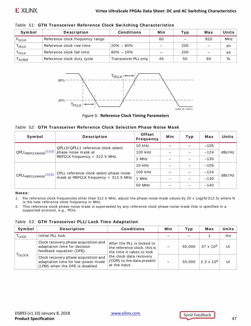
Virtex UltraScale FPGAs Data Sheet: DC and AC Switching Characteristics
DS893 (v1.10) January 8, 2018 www.xilinx.comProduct Specification 47
Table 51: GTH Transceiver Reference Clock Switching Characteristics
Symbol Description Conditions Min Typ Max UnitsFGCLK Reference clock frequency range 60 – 820 MHz
TRCLK Reference clock rise time 20% – 80% – 200 – ps
TFCLK Reference clock fall time 80% – 20% – 200 – ps
TDCREF Reference clock duty cycle Transceiver PLL only 40 50 60 %
X-Ref Target - Figure 5
Figure 5: Reference Clock Timing Parameters
Table 52: GTH Transceiver Reference Clock Selection Phase Noise Mask
Symbol Description Offset Frequency Min Typ Max Units
QPLLREFCLKMASK(1)(2)
QPLL0/QPLL1 reference clock select phase noise mask at REFCLK frequency = 312.5 MHz.
10 kHz – – –105
dBc/Hz100 kHz – – –124
1 MHz – – –130
CPLLREFCLKMASK(1)(2) CPLL reference clock select phase noise
mask at REFCLK frequency = 312.5 MHz.
10 kHz – – –105
dBc/Hz100 kHz – – –124
1 MHz – – –130
50 MHz – – –140
Notes: 1. For reference clock frequencies other than 312.5 MHz, adjust the phase-noise mask values by 20 x Log(N/312.5) where N
is the new reference clock frequency in MHz.2. This reference clock phase-noise mask is superseded by any reference clock phase-noise mask that is specified in a
supported protocol, e.g., PCIe.
Table 53: GTH Transceiver PLL/Lock Time Adaptation
Symbol Description Conditions Min Typ Max UnitsTLOCK Initial PLL lock. – – 1 ms
TDLOCK
Clock recovery phase acquisition and adaptation time for decision feedback equalizer (DFE).
After the PLL is locked to the reference clock, this is the time it takes to lock the clock data recovery (CDR) to the data present at the input.
– 50,000 37 x 106 UI
Clock recovery phase acquisition and adaptation time for low-power mode (LPM) when the DFE is disabled.
– 50,000 2.3 x 10⁶ UI
ds893_05_120314
80%
20% T FCLK
T RCLK
Send Feedback

Virtex UltraScale FPGAs Data Sheet: DC and AC Switching Characteristics
DS893 (v1.10) January 8, 2018 www.xilinx.comProduct Specification 48
Table 54: GTH Transceiver User Clock Switching Characteristics(1)
Symbol Description
Data Width Conditions(Bit)
Speed Grades and VCCINT Operating Voltages
Units1.0V 0.95V
Internal Logic
Interconnect Logic -3 -1H -2 -1
FTXOUTPMATXOUTCLK maximum frequency sourced from OUTCLKPMA. 511.719 511.719 511.719 390.625 MHz
FRXOUTPMARXOUTCLK maximum frequency sourced from OUTCLKPMA. 511.719 511.719 511.719 390.625 MHz
FTXOUTPROGDIVTXOUTCLK maximum frequency sourced from TXPROGDIVCLK. 511.719 511.719 511.719 511.719 MHz
FRXOUTPROGDIVRXOUTCLK maximum frequency sourced from RXPROGDIVCLK. 511.719 511.719 511.719 511.719 MHz
FTXIN
TXUSRCLK maximum frequency
16 16, 32 511.719 511.719 511.719 390.625 MHz
32 32, 64 511.719 511.719 511.719 390.625 MHz
20 20, 40 409.375 409.375 409.375 312.500 MHz
40 40, 80 409.375 409.375 409.375 312.500 MHz
FRXIN
RXUSRCLK maximum frequency
16 16, 32 511.719 511.719 511.719 390.625 MHz
32 32, 64 511.719 511.719 511.719 390.625 MHz
20 20, 40 409.375 409.375 409.375 312.500 MHz
40 40, 80 409.375 409.375 409.375 312.500 MHz
FTXIN2
TXUSRCLK2 maximum frequency
16 16 511.719 511.719 511.719 390.625 MHz
16, 32 32 511.719 511.719 511.719 390.625 MHz
32 64 255.860 255.860 255.860 195.313 MHz
20 20 409.375 409.375 409.375 312.500 MHz
20, 40 40 409.375 409.375 409.375 312.500 MHz
40 80 204.688 204.688 204.688 156.250 MHz
FRXIN2
RXUSRCLK2 maximum frequency
16 16 511.719 511.719 511.719 390.625 MHz
16, 32 32 511.719 511.719 511.719 390.625 MHz
32 64 255.860 255.860 255.860 195.313 MHz
20 20 409.375 409.375 409.375 312.500 MHz
20, 40 40 409.375 409.375 409.375 312.500 MHz
40 80 204.688 204.688 204.688 156.250 MHz
Notes: 1. Clocking must be implemented as described in UltraScale Architecture GTH Transceiver User Guide (UG576).
Send Feedback
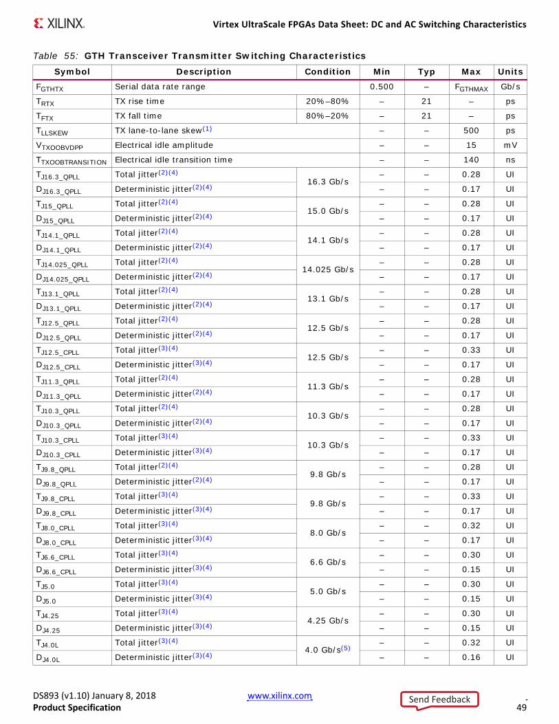
Virtex UltraScale FPGAs Data Sheet: DC and AC Switching Characteristics
DS893 (v1.10) January 8, 2018 www.xilinx.comProduct Specification 49
Table 55: GTH Transceiver Transmitter Switching Characteristics
Symbol Description Condition Min Typ Max UnitsFGTHTX Serial data rate range 0.500 – FGTHMAX Gb/s
TRTX TX rise time 20%–80% – 21 – ps
TFTX TX fall time 80%–20% – 21 – ps
TLLSKEW TX lane-to-lane skew(1) – – 500 ps
VTXOOBVDPP Electrical idle amplitude – – 15 mV
TTXOOBTRANSITION Electrical idle transition time – – 140 ns
TJ16.3_QPLL Total jitter(2)(4)16.3 Gb/s
– – 0.28 UI
DJ16.3_QPLL Deterministic jitter(2)(4) – – 0.17 UI
TJ15_QPLL Total jitter(2)(4)15.0 Gb/s
– – 0.28 UI
DJ15_QPLL Deterministic jitter(2)(4) – – 0.17 UI
TJ14.1_QPLL Total jitter(2)(4)14.1 Gb/s
– – 0.28 UI
DJ14.1_QPLL Deterministic jitter(2)(4) – – 0.17 UI
TJ14.025_QPLL Total jitter(2)(4)14.025 Gb/s
– – 0.28 UI
DJ14.025_QPLL Deterministic jitter(2)(4) – – 0.17 UI
TJ13.1_QPLL Total jitter(2)(4)13.1 Gb/s
– – 0.28 UI
DJ13.1_QPLL Deterministic jitter(2)(4) – – 0.17 UI
TJ12.5_QPLL Total jitter(2)(4)12.5 Gb/s
– – 0.28 UI
DJ12.5_QPLL Deterministic jitter(2)(4) – – 0.17 UI
TJ12.5_CPLL Total jitter(3)(4)12.5 Gb/s
– – 0.33 UI
DJ12.5_CPLL Deterministic jitter(3)(4) – – 0.17 UI
TJ11.3_QPLL Total jitter(2)(4)11.3 Gb/s
– – 0.28 UI
DJ11.3_QPLL Deterministic jitter(2)(4) – – 0.17 UI
TJ10.3_QPLL Total jitter(2)(4)10.3 Gb/s
– – 0.28 UI
DJ10.3_QPLL Deterministic jitter(2)(4) – – 0.17 UI
TJ10.3_CPLL Total jitter(3)(4)10.3 Gb/s
– – 0.33 UI
DJ10.3_CPLL Deterministic jitter(3)(4) – – 0.17 UI
TJ9.8_QPLL Total jitter(2)(4)9.8 Gb/s
– – 0.28 UI
DJ9.8_QPLL Deterministic jitter(2)(4) – – 0.17 UI
TJ9.8_CPLL Total jitter(3)(4)9.8 Gb/s
– – 0.33 UI
DJ9.8_CPLL Deterministic jitter(3)(4) – – 0.17 UI
TJ8.0_CPLL Total jitter(3)(4)8.0 Gb/s
– – 0.32 UI
DJ8.0_CPLL Deterministic jitter(3)(4) – – 0.17 UI
TJ6.6_CPLL Total jitter(3)(4)6.6 Gb/s
– – 0.30 UI
DJ6.6_CPLL Deterministic jitter(3)(4) – – 0.15 UI
TJ5.0 Total jitter(3)(4)5.0 Gb/s
– – 0.30 UI
DJ5.0 Deterministic jitter(3)(4) – – 0.15 UI
TJ4.25 Total jitter(3)(4)4.25 Gb/s
– – 0.30 UI
DJ4.25 Deterministic jitter(3)(4) – – 0.15 UI
TJ4.0L Total jitter(3)(4)4.0 Gb/s(5)
– – 0.32 UI
DJ4.0L Deterministic jitter(3)(4) – – 0.16 UI
Send Feedback
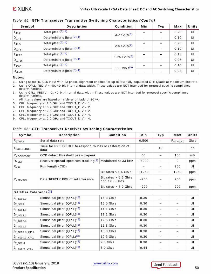
Virtex UltraScale FPGAs Data Sheet: DC and AC Switching Characteristics
DS893 (v1.10) January 8, 2018 www.xilinx.comProduct Specification 50
TJ3.2 Total jitter(3)(4)3.2 Gb/s(6)
– – 0.20 UI
DJ3.2 Deterministic jitter(3)(4) – – 0.10 UI
TJ2.5 Total jitter(3)(4)2.5 Gb/s(7)
– – 0.20 UI
DJ2.5 Deterministic jitter(3)(4) – – 0.10 UI
TJ1.25 Total jitter(3)(4)1.25 Gb/s(8)
– – 0.15 UI
DJ1.25 Deterministic jitter(3)(4) – – 0.06 UI
TJ500 Total jitter(3)(4)500 Mb/s(9)
– – 0.10 UI
DJ500 Deterministic jitter(3)(4) – – 0.03 UI
Notes: 1. Using same REFCLK input with TX phase alignment enabled for up to four fully populated GTH Quads at maximum line rate.2. Using QPLL_FBDIV = 40, 40-bit internal data width. These values are NOT intended for protocol specific compliance
determinations.3. Using CPLL_FBDIV = 2, 40-bit internal data width. These values are NOT intended for protocol specific compliance
determinations.4. All jitter values are based on a bit-error ratio of 10-12.5. CPLL frequency at 2.0 GHz and TXOUT_DIV = 1.6. CPLL frequency at 3.2 GHz and TXOUT_DIV = 2.7. CPLL frequency at 2.5 GHz and TXOUT_DIV = 2.8. CPLL frequency at 2.5 GHz and TXOUT_DIV = 4.9. CPLL frequency at 2.0 GHz and TXOUT_DIV = 4.
Table 56: GTH Transceiver Receiver Switching Characteristics
Symbol Description Condition Min Typ Max UnitsFGTHRX Serial data rate 0.500 – FGTHMAX Gb/s
TRXELECIDLETime for RXELECIDLE to respond to loss or restoration of data – 10 – ns
RXOOBVDPP OOB detect threshold peak-to-peak 60 – 150 mV
RXSST Receiver spread-spectrum tracking(1) Modulated at 33 kHz –5000 – 0 ppm
RXRL Run length (CID) – – 256 UI
RXPPMTOL Data/REFCLK PPM offset tolerance
Bit rates ≤ 6.6 Gb/s –1250 – 1250 ppm
Bit rates > 6.6 Gb/s and ≤ 8.0 Gb/s –700 – 700 ppm
Bit rates > 8.0 Gb/s –200 – 200 ppm
SJ Jitter Tolerance(2)
JT_SJ16.3 Sinusoidal jitter (QPLL)(3) 16.3 Gb/s 0.30 – – UI
JT_SJ15 Sinusoidal jitter (QPLL)(3) 15.0 Gb/s 0.30 – – UI
JT_SJ14.1 Sinusoidal jitter (QPLL)(3) 14.1 Gb/s 0.30 – – UI
JT_SJ13.1 Sinusoidal jitter (QPLL)(3) 13.1 Gb/s 0.30 – – UI
JT_SJ12.5 Sinusoidal jitter (QPLL)(3) 12.5 Gb/s 0.30 – – UI
JT_SJ11.3 Sinusoidal jitter (QPLL)(3) 11.3 Gb/s 0.30 – – UI
JT_SJ10.3_QPLL Sinusoidal jitter (QPLL)(3) 10.3 Gb/s 0.30 – – UI
JT_SJ10.3_CPLL Sinusoidal jitter (CPLL)(3) 10.3 Gb/s 0.30 – – UI
JT_SJ9.8 Sinusoidal jitter (QPLL)(3) 9.8 Gb/s 0.30 – – UI
JT_SJ8.0_QPLL Sinusoidal jitter (QPLL)(3) 8.0 Gb/s 0.44 – – UI
Table 55: GTH Transceiver Transmitter Switching Characteristics (Cont’d)
Symbol Description Condition Min Typ Max Units
Send Feedback
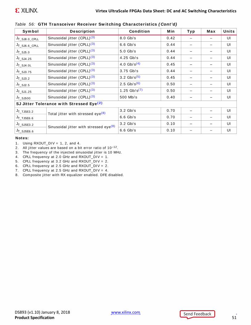
Virtex UltraScale FPGAs Data Sheet: DC and AC Switching Characteristics
DS893 (v1.10) January 8, 2018 www.xilinx.comProduct Specification 51
JT_SJ8.0_CPLL Sinusoidal jitter (CPLL)(3) 8.0 Gb/s 0.42 – – UI
JT_SJ6.6_CPLL Sinusoidal jitter (CPLL)(3) 6.6 Gb/s 0.44 – – UI
JT_SJ5.0 Sinusoidal jitter (CPLL)(3) 5.0 Gb/s 0.44 – – UI
JT_SJ4.25 Sinusoidal jitter (CPLL)(3) 4.25 Gb/s 0.44 – – UI
JT_SJ4.0L Sinusoidal jitter (CPLL)(3) 4.0 Gb/s(4) 0.45 – – UI
JT_SJ3.75 Sinusoidal jitter (CPLL)(3) 3.75 Gb/s 0.44 – – UI
JT_SJ3.2 Sinusoidal jitter (CPLL)(3) 3.2 Gb/s(5) 0.45 – – UI
JT_SJ2.5 Sinusoidal jitter (CPLL)(3) 2.5 Gb/s(6) 0.50 – – UI
JT_SJ1.25 Sinusoidal jitter (CPLL)(3) 1.25 Gb/s(7) 0.50 – – UI
JT_SJ500 Sinusoidal jitter (CPLL)(3) 500 Mb/s 0.40 – – UI
SJ Jitter Tolerance with Stressed Eye(2)
JT_TJSE3.2 Total jitter with stressed eye(8)3.2 Gb/s 0.70 – – UI
JT_TJSE6.6 6.6 Gb/s 0.70 – – UI
JT_SJSE3.2 Sinusoidal jitter with stressed eye(8)3.2 Gb/s 0.10 – – UI
JT_SJSE6.6 6.6 Gb/s 0.10 – – UI
Notes: 1. Using RXOUT_DIV = 1, 2, and 4.2. All jitter values are based on a bit error ratio of 10–12.3. The frequency of the injected sinusoidal jitter is 10 MHz.4. CPLL frequency at 2.0 GHz and RXOUT_DIV = 1.5. CPLL frequency at 3.2 GHz and RXOUT_DIV = 2.6. CPLL frequency at 2.5 GHz and RXOUT_DIV = 2.7. CPLL frequency at 2.5 GHz and RXOUT_DIV = 4.8. Composite jitter with RX equalizer enabled. DFE disabled.
Table 56: GTH Transceiver Receiver Switching Characteristics (Cont’d)
Symbol Description Condition Min Typ Max Units
Send Feedback
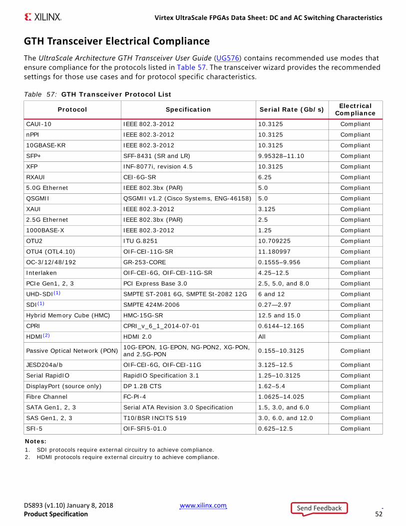
Virtex UltraScale FPGAs Data Sheet: DC and AC Switching Characteristics
DS893 (v1.10) January 8, 2018 www.xilinx.comProduct Specification 52
GTH Transceiver Electrical ComplianceThe UltraScale Architecture GTH Transceiver User Guide (UG576) contains recommended use modes that ensure compliance for the protocols listed in Table 57. The transceiver wizard provides the recommended settings for those use cases and for protocol specific characteristics.
Table 57: GTH Transceiver Protocol List
Protocol Specification Serial Rate (Gb/s) Electrical Compliance
CAUI-10 IEEE 802.3-2012 10.3125 Compliant
nPPI IEEE 802.3-2012 10.3125 Compliant
10GBASE-KR IEEE 802.3-2012 10.3125 Compliant
SFP+ SFF-8431 (SR and LR) 9.95328–11.10 Compliant
XFP INF-8077i, revision 4.5 10.3125 Compliant
RXAUI CEI-6G-SR 6.25 Compliant
5.0G Ethernet IEEE 802.3bx (PAR) 5.0 Compliant
QSGMII QSGMII v1.2 (Cisco Systems, ENG-46158) 5.0 Compliant
XAUI IEEE 802.3-2012 3.125 Compliant
2.5G Ethernet IEEE 802.3bx (PAR) 2.5 Compliant
1000BASE-X IEEE 802.3-2012 1.25 Compliant
OTU2 ITU G.8251 10.709225 Compliant
OTU4 (OTL4.10) OIF-CEI-11G-SR 11.180997 Compliant
OC-3/12/48/192 GR-253-CORE 0.1555–9.956 Compliant
Interlaken OIF-CEI-6G, OIF-CEI-11G-SR 4.25–12.5 Compliant
PCIe Gen1, 2, 3 PCI Express Base 3.0 2.5, 5.0, and 8.0 Compliant
UHD-SDI(1) SMPTE ST-2081 6G, SMPTE St-2082 12G 6 and 12 Compliant
SDI(1) SMPTE 424M-2006 0.27—2.97 Compliant
Hybrid Memory Cube (HMC) HMC-15G-SR 12.5 and 15.0 Compliant
CPRI CPRI_v_6_1_2014-07-01 0.6144–12.165 Compliant
HDMI(2) HDMI 2.0 All Compliant
Passive Optical Network (PON) 10G-EPON, 1G-EPON, NG-PON2, XG-PON, and 2.5G-PON 0.155–10.3125 Compliant
JESD204a/b OIF-CEI-6G, OIF-CEI-11G 3.125–12.5 Compliant
Serial RapidIO RapidIO Specification 3.1 1.25–10.3125 Compliant
DisplayPort (source only) DP 1.2B CTS 1.62–5.4 Compliant
Fibre Channel FC-PI-4 1.0625–14.025 Compliant
SATA Gen1, 2, 3 Serial ATA Revision 3.0 Specification 1.5, 3.0, and 6.0 Compliant
SAS Gen1, 2, 3 T10/BSR INCITS 519 3.0, 6.0, and 12.0 Compliant
SFI-5 OIF-SFI5-01.0 0.625–12.5 Compliant
Notes: 1. SDI protocols require external circuitry to achieve compliance.2. HDMI protocols require external circuitry to achieve compliance.
Send Feedback
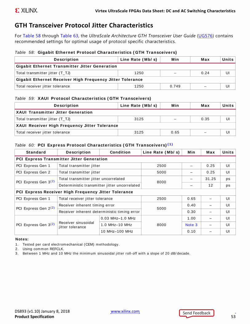
Virtex UltraScale FPGAs Data Sheet: DC and AC Switching Characteristics
DS893 (v1.10) January 8, 2018 www.xilinx.comProduct Specification 53
GTH Transceiver Protocol Jitter CharacteristicsFor Table 58 through Table 63, the UltraScale Architecture GTH Transceiver User Guide (UG576) contains recommended settings for optimal usage of protocol specific characteristics.
Table 58: Gigabit Ethernet Protocol Characteristics (GTH Transceivers)
Description Line Rate (Mb/s) Min Max Units
Gigabit Ethernet Transmitter Jitter GenerationTotal transmitter jitter (T_TJ) 1250 – 0.24 UI
Gigabit Ethernet Receiver High Frequency Jitter ToleranceTotal receiver jitter tolerance 1250 0.749 – UI
Table 59: XAUI Protocol Characteristics (GTH Transceivers)
Description Line Rate (Mb/s) Min Max Units
XAUI Transmitter Jitter GenerationTotal transmitter jitter (T_TJ) 3125 – 0.35 UI
XAUI Receiver High Frequency Jitter ToleranceTotal receiver jitter tolerance 3125 0.65 – UI
Table 60: PCI Express Protocol Characteristics (GTH Transceivers)(1)
Standard Description Condition Line Rate (Mb/s) Min Max Units
PCI Express Transmitter Jitter GenerationPCI Express Gen 1 Total transmitter jitter 2500 – 0.25 UI
PCI Express Gen 2 Total transmitter jitter 5000 – 0.25 UI
PCI Express Gen 3(2)Total transmitter jitter uncorrelated
8000– 31.25 ps
Deterministic transmitter jitter uncorrelated – 12 ps
PCI Express Receiver High Frequency Jitter TolerancePCI Express Gen 1 Total receiver jitter tolerance 2500 0.65 – UI
PCI Express Gen 2(2)Receiver inherent timing error
50000.40 – UI
Receiver inherent deterministic timing error 0.30 – UI
PCI Express Gen 3(2) Receiver sinusoidal jitter tolerance
0.03 MHz–1.0 MHz
8000
1.00 – UI
1.0 MHz–10 MHz Note 3 – UI
10 MHz–100 MHz 0.10 – UI
Notes: 1. Tested per card electromechanical (CEM) methodology.2. Using common REFCLK.3. Between 1 MHz and 10 MHz the minimum sinusoidal jitter roll-off with a slope of 20 dB/decade.
Send Feedback
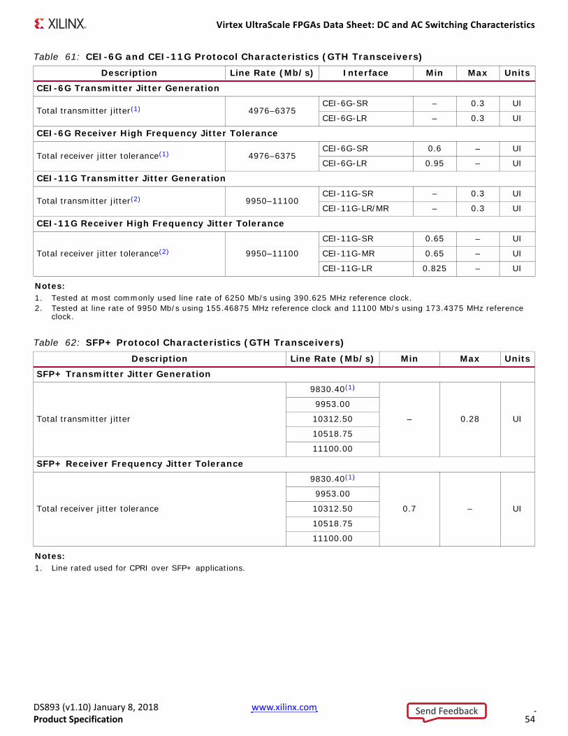
Virtex UltraScale FPGAs Data Sheet: DC and AC Switching Characteristics
DS893 (v1.10) January 8, 2018 www.xilinx.comProduct Specification 54
Table 61: CEI-6G and CEI-11G Protocol Characteristics (GTH Transceivers)
Description Line Rate (Mb/s) Interface Min Max Units
CEI-6G Transmitter Jitter Generation
Total transmitter jitter(1) 4976–6375CEI-6G-SR – 0.3 UI
CEI-6G-LR – 0.3 UI
CEI-6G Receiver High Frequency Jitter Tolerance
Total receiver jitter tolerance(1) 4976–6375CEI-6G-SR 0.6 – UI
CEI-6G-LR 0.95 – UI
CEI-11G Transmitter Jitter Generation
Total transmitter jitter(2) 9950–11100CEI-11G-SR – 0.3 UI
CEI-11G-LR/MR – 0.3 UI
CEI-11G Receiver High Frequency Jitter Tolerance
Total receiver jitter tolerance(2) 9950–11100
CEI-11G-SR 0.65 – UI
CEI-11G-MR 0.65 – UI
CEI-11G-LR 0.825 – UI
Notes: 1. Tested at most commonly used line rate of 6250 Mb/s using 390.625 MHz reference clock.2. Tested at line rate of 9950 Mb/s using 155.46875 MHz reference clock and 11100 Mb/s using 173.4375 MHz reference
clock.
Table 62: SFP+ Protocol Characteristics (GTH Transceivers)
Description Line Rate (Mb/s) Min Max Units
SFP+ Transmitter Jitter Generation
Total transmitter jitter
9830.40(1)
– 0.28 UI
9953.00
10312.50
10518.75
11100.00
SFP+ Receiver Frequency Jitter Tolerance
Total receiver jitter tolerance
9830.40(1)
0.7 – UI
9953.00
10312.50
10518.75
11100.00
Notes: 1. Line rated used for CPRI over SFP+ applications.
Send Feedback

Virtex UltraScale FPGAs Data Sheet: DC and AC Switching Characteristics
DS893 (v1.10) January 8, 2018 www.xilinx.comProduct Specification 55
Table 63: CPRI Protocol Characteristics (GTH Transceivers)
Description Line Rate (Mb/s) Min Max Units
CPRI Transmitter Jitter Generation
Total transmitter jitter
614.4 – 0.35 UI
1228.8 – 0.35 UI
2457.6 – 0.35 UI
3072.0 – 0.35 UI
4915.2 – 0.3 UI
6144.0 – 0.3 UI
9830.4 – Note 1 UI
CPRI Receiver Frequency Jitter Tolerance
Total receiver jitter tolerance
614.4 0.65 – UI
1228.8 0.65 – UI
2457.6 0.65 – UI
3072.0 0.65 – UI
4915.2 0.95 – UI
6144.0 0.95 – UI
9830.4 Note 1 – UI
Notes: 1. Tested per SFP+ specification, see Table 62.
Send Feedback

Virtex UltraScale FPGAs Data Sheet: DC and AC Switching Characteristics
DS893 (v1.10) January 8, 2018 www.xilinx.comProduct Specification 56
GTY Transceiver Specifications
GTY Transceiver DC Input and Output LevelsTable 64 summarizes the DC specifications of the GTY transceivers in Virtex UltraScale FPGAs. Consult www.xilinx.com/products/technology/high-speed-serial for further details.
Table 64: GTY Transceiver DC Specifications
Symbol DC Parameter Conditions Min Typ Max Units
DVPPINDifferential peak-to-peak input voltage (external AC coupled)
>10.3125 Gb/s 150 – 1250 mV
6.6 Gb/s to 10.3125 Gb/s 150 – 1250 mV
≤ 6.6 Gb/s 150 – 2000 mV
VIN
Single-ended input voltage. Voltage measured at the pin referenced to GND.
DC coupled VMGTAVTT = 1.2V –400 – VMGTAVTT mV
VCMIN Common mode input voltage DC coupled VMGTAVTT = 1.2V – 2/3 VMGTAVTT – mV
DVPPOUTDifferential peak-to-peak output voltage(1)
Transmitter output swing is set to 0x1F 800 – – mV
VCMOUTDCCommon mode output voltage: DC coupled (equation based)
When remote RX is terminated to GND VMGTAVTT/2 – DVPPOUT/4 mV
When remote RX termination is floating VMGTAVTT – DVPPOUT/2 mV
When remote RX is terminated to VRX_TERM
(2) mV
VCMOUTACCommon mode output voltage: AC coupled Equation based VMGTAVTT – DVPPOUT/2 mV
RIN Differential input resistance – 100 – Ω
ROUT Differential output resistance – 100 – Ω
TOSKEW Transmitter output pair (TXP and TXN) intra-pair skew – – 5 ps
CEXT Recommended external AC coupling capacitor(3) – 100 – nF
Notes: 1. The output swing and pre-emphasis levels are programmable using the GTY transceiver attributes and can result in values
lower than reported in this table.2. VRX_TERM is the remote RX termination voltage.3. Other values can be used as appropriate to conform to specific protocols and standards.
X-Ref Target - Figure 6
Figure 6: Single-Ended Peak-to-Peak Voltage
VMGTAVTTDVPPOUT
4----------------------–
VMGTAVTT VRX_TERM–
2------------------------------------------------------- –
0
+V P
N
ds893_03_120314
Single-EndedPeak-to-Peak Voltage
Send Feedback

Virtex UltraScale FPGAs Data Sheet: DC and AC Switching Characteristics
DS893 (v1.10) January 8, 2018 www.xilinx.comProduct Specification 57
Table 65 summarizes the DC specifications of the clock input of the GTY transceivers in Virtex UltraScale FPGAs. Consult www.xilinx.com/products/technology/high-speed-serial for further details.
X-Ref Target - Figure 7
Figure 7: Differential Peak-to-Peak Voltage
Table 65: GTY Transceiver Clock DC Input Level Specification
Symbol DC Parameter Min Typ Max UnitsVIDIFF Differential peak-to-peak input voltage 250 – 2000 mV
RIN Differential input resistance – 100 – Ω
CEXT Required external AC coupling capacitor – 10 – nF
Table 66: GTY Transceiver Clock Output Level Specification
Symbol Description Conditions Min Typ Max UnitsVOL Output Low voltage for P and N RT = 100Ω across P and N signals – 400 – mV
VOH Output High voltage for P and N RT = 100Ω across P and N signals – 760 – mV
VDDOUT
Differential output voltage (P–N), P = High (N–P), N = High
RT = 100Ω across P and N signals – ±360 – mV
VCMOUT Common mode voltage RT = 100Ω across P and N signals – 580 – mV
0
+V
–V P–Nds893_04_120314
Differential peak-to-peak voltage = (Single-ended peak-to-peak voltage) x 2
DifferentialPeak-to-Peak
Voltage
Send Feedback
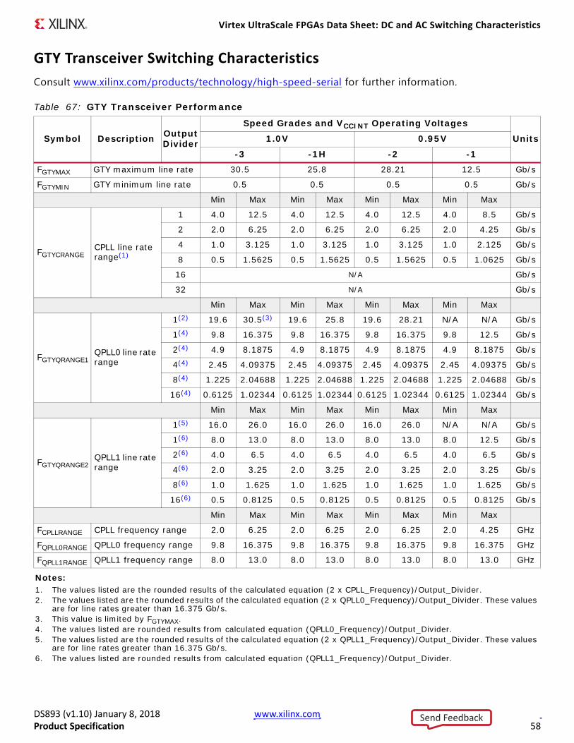
Virtex UltraScale FPGAs Data Sheet: DC and AC Switching Characteristics
DS893 (v1.10) January 8, 2018 www.xilinx.comProduct Specification 58
GTY Transceiver Switching CharacteristicsConsult www.xilinx.com/products/technology/high-speed-serial for further information.
Table 67: GTY Transceiver Performance
Symbol Description Output Divider
Speed Grades and VCCINT Operating Voltages
Units1.0V 0.95V
-3 -1H -2 -1FGTYMAX GTY maximum line rate 30.5 25.8 28.21 12.5 Gb/s
FGTYMIN GTY minimum line rate 0.5 0.5 0.5 0.5 Gb/s
Min Max Min Max Min Max Min Max
FGTYCRANGECPLL line rate range(1)
1 4.0 12.5 4.0 12.5 4.0 12.5 4.0 8.5 Gb/s
2 2.0 6.25 2.0 6.25 2.0 6.25 2.0 4.25 Gb/s
4 1.0 3.125 1.0 3.125 1.0 3.125 1.0 2.125 Gb/s
8 0.5 1.5625 0.5 1.5625 0.5 1.5625 0.5 1.0625 Gb/s
16 N/A Gb/s
32 N/A Gb/s
Min Max Min Max Min Max Min Max
FGTYQRANGE1QPLL0 line rate range
1(2) 19.6 30.5(3) 19.6 25.8 19.6 28.21 N/A N/A Gb/s
1(4) 9.8 16.375 9.8 16.375 9.8 16.375 9.8 12.5 Gb/s
2(4) 4.9 8.1875 4.9 8.1875 4.9 8.1875 4.9 8.1875 Gb/s
4(4) 2.45 4.09375 2.45 4.09375 2.45 4.09375 2.45 4.09375 Gb/s
8(4) 1.225 2.04688 1.225 2.04688 1.225 2.04688 1.225 2.04688 Gb/s
16(4) 0.6125 1.02344 0.6125 1.02344 0.6125 1.02344 0.6125 1.02344 Gb/s
Min Max Min Max Min Max Min Max
FGTYQRANGE2QPLL1 line rate range
1(5) 16.0 26.0 16.0 26.0 16.0 26.0 N/A N/A Gb/s
1(6) 8.0 13.0 8.0 13.0 8.0 13.0 8.0 12.5 Gb/s
2(6) 4.0 6.5 4.0 6.5 4.0 6.5 4.0 6.5 Gb/s
4(6) 2.0 3.25 2.0 3.25 2.0 3.25 2.0 3.25 Gb/s
8(6) 1.0 1.625 1.0 1.625 1.0 1.625 1.0 1.625 Gb/s
16(6) 0.5 0.8125 0.5 0.8125 0.5 0.8125 0.5 0.8125 Gb/s
Min Max Min Max Min Max Min Max
FCPLLRANGE CPLL frequency range 2.0 6.25 2.0 6.25 2.0 6.25 2.0 4.25 GHz
FQPLL0RANGE QPLL0 frequency range 9.8 16.375 9.8 16.375 9.8 16.375 9.8 16.375 GHz
FQPLL1RANGE QPLL1 frequency range 8.0 13.0 8.0 13.0 8.0 13.0 8.0 13.0 GHz
Notes: 1. The values listed are the rounded results of the calculated equation (2 x CPLL_Frequency)/Output_Divider.2. The values listed are the rounded results of the calculated equation (2 x QPLL0_Frequency)/Output_Divider. These values
are for line rates greater than 16.375 Gb/s.3. This value is limited by FGTYMAX.4. The values listed are rounded results from calculated equation (QPLL0_Frequency)/Output_Divider.5. The values listed are the rounded results of the calculated equation (2 x QPLL1_Frequency)/Output_Divider. These values
are for line rates greater than 16.375 Gb/s.6. The values listed are rounded results from calculated equation (QPLL1_Frequency)/Output_Divider.
Send Feedback
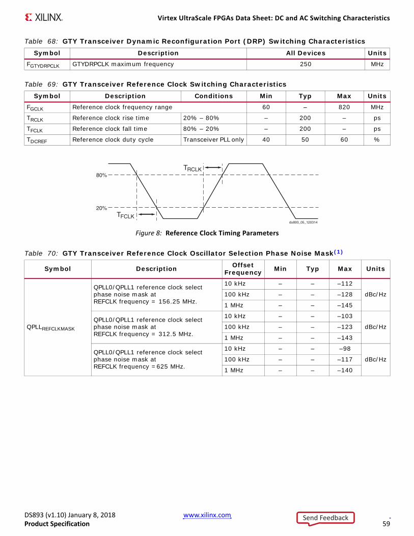
Virtex UltraScale FPGAs Data Sheet: DC and AC Switching Characteristics
DS893 (v1.10) January 8, 2018 www.xilinx.comProduct Specification 59
Table 68: GTY Transceiver Dynamic Reconfiguration Port (DRP) Switching Characteristics
Symbol Description All Devices UnitsFGTYDRPCLK GTYDRPCLK maximum frequency 250 MHz
Table 69: GTY Transceiver Reference Clock Switching Characteristics
Symbol Description Conditions Min Typ Max UnitsFGCLK Reference clock frequency range 60 – 820 MHz
TRCLK Reference clock rise time 20% – 80% – 200 – ps
TFCLK Reference clock fall time 80% – 20% – 200 – ps
TDCREF Reference clock duty cycle Transceiver PLL only 40 50 60 %
X-Ref Target - Figure 8
Figure 8: Reference Clock Timing Parameters
Table 70: GTY Transceiver Reference Clock Oscillator Selection Phase Noise Mask(1)
Symbol Description Offset Frequency Min Typ Max Units
QPLLREFCLKMASK
QPLL0/QPLL1 reference clock select phase noise mask at REFCLK frequency = 156.25 MHz.
10 kHz – – –112
dBc/Hz100 kHz – – –128
1 MHz – – –145
QPLL0/QPLL1 reference clock select phase noise mask at REFCLK frequency = 312.5 MHz.
10 kHz – – –103
dBc/Hz100 kHz – – –123
1 MHz – – –143
QPLL0/QPLL1 reference clock select phase noise mask at REFCLK frequency =625 MHz.
10 kHz – – –98
dBc/Hz100 kHz – – –117
1 MHz – – –140
ds893_05_120314
80%
20% T FCLK
T RCLK
Send Feedback
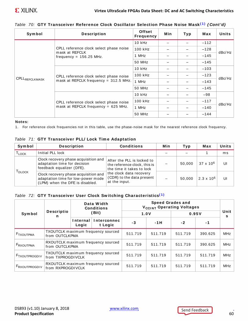
Virtex UltraScale FPGAs Data Sheet: DC and AC Switching Characteristics
DS893 (v1.10) January 8, 2018 www.xilinx.comProduct Specification 60
CPLLREFCLKMASK
CPLL reference clock select phase noise mask at REFCLK frequency = 156.25 MHz.
10 kHz – – –112
dBc/Hz100 kHz – – –128
1 MHz – – –145
50 MHz – – –145
CPLL reference clock select phase noise mask at REFCLK frequency = 312.5 MHz.
10 kHz – – –103
dBc/Hz100 kHz – – –123
1 MHz – – –143
50 MHz – – –145
CPLL reference clock select phase noise mask at REFCLK frequency = 625 MHz.
10 kHz – – –98
dBc/Hz100 kHz – – –117
1 MHz – – –140
50 MHz – – –144
Notes: 1. For reference clock frequencies not in this table, use the phase-noise mask for the nearest reference clock frequency.
Table 71: GTY Transceiver PLL/Lock Time Adaptation
Symbol Description Conditions Min Typ Max UnitsTLOCK Initial PLL lock – – 1 ms
TDLOCK
Clock recovery phase acquisition and adaptation time for decision feedback equalizer (DFE).
After the PLL is locked to the reference clock, this is the time it takes to lock the clock data recovery (CDR) to the data present at the input.
– 50,000 37 x 106 UI
Clock recovery phase acquisition and adaptation time for low-power mode (LPM) when the DFE is disabled.
– 50,000 2.3 x 10⁶ UI
Table 72: GTY Transceiver User Clock Switching Characteristics(1)
Symbol Description
Data Width Conditions
(Bit)
Speed Grades and VCCINT Operating Voltages
Units1.0V 0.95V
Internal Logic
Interconnect Logic -3 -1H -2 -1
FTXOUTPMATXOUTCLK maximum frequency sourced from OUTCLKPMA 511.719 511.719 511.719 390.625 MHz
FRXOUTPMARXOUTCLK maximum frequency sourced from OUTCLKPMA 511.719 511.719 511.719 390.625 MHz
FTXOUTPROGDIVTXOUTCLK maximum frequency sourced from TXPROGDIVCLK 511.719 511.719 511.719 511.719 MHz
FRXOUTPROGDIVRXOUTCLK maximum frequency sourced from RXPROGDIVCLK 511.719 511.719 511.719 511.719 MHz
Table 70: GTY Transceiver Reference Clock Oscillator Selection Phase Noise Mask(1) (Cont’d)
Symbol Description Offset Frequency Min Typ Max Units
Send Feedback
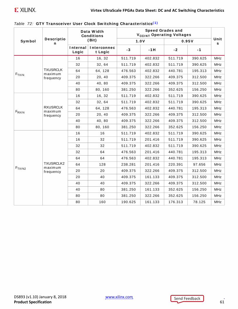
Virtex UltraScale FPGAs Data Sheet: DC and AC Switching Characteristics
DS893 (v1.10) January 8, 2018 www.xilinx.comProduct Specification 61
FTXIN
TXUSRCLK maximum frequency
16 16, 32 511.719 402.832 511.719 390.625 MHz
32 32, 64 511.719 402.832 511.719 390.625 MHz
64 64, 128 476.563 402.832 440.781 195.313 MHz
20 20, 40 409.375 322.266 409.375 312.500 MHz
40 40, 80 409.375 322.266 409.375 312.500 MHz
80 80, 160 381.250 322.266 352.625 156.250 MHz
FRXIN
RXUSRCLK maximum frequency
16 16, 32 511.719 402.832 511.719 390.625 MHz
32 32, 64 511.719 402.832 511.719 390.625 MHz
64 64, 128 476.563 402.832 440.781 195.313 MHz
20 20, 40 409.375 322.266 409.375 312.500 MHz
40 40, 80 409.375 322.266 409.375 312.500 MHz
80 80, 160 381.250 322.266 352.625 156.250 MHz
FTXIN2
TXUSRCLK2 maximum frequency
16 16 511.719 402.832 511.719 390.625 MHz
16 32 511.719 201.416 511.719 390.625 MHz
32 32 511.719 402.832 511.719 390.625 MHz
32 64 476.563 201.416 440.781 195.313 MHz
64 64 476.563 402.832 440.781 195.313 MHz
64 128 238.281 201.416 220.391 97.656 MHz
20 20 409.375 322.266 409.375 312.500 MHz
20 40 409.375 161.133 409.375 312.500 MHz
40 40 409.375 322.266 409.375 312.500 MHz
40 80 381.250 161.133 352.625 156.250 MHz
80 80 381.250 322.266 352.625 156.250 MHz
80 160 190.625 161.133 176.313 78.125 MHz
Table 72: GTY Transceiver User Clock Switching Characteristics(1)
Symbol Description
Data Width Conditions
(Bit)
Speed Grades and VCCINT Operating Voltages
Units1.0V 0.95V
Internal Logic
Interconnect Logic -3 -1H -2 -1
Send Feedback

Virtex UltraScale FPGAs Data Sheet: DC and AC Switching Characteristics
DS893 (v1.10) January 8, 2018 www.xilinx.comProduct Specification 62
FRXIN2
RXUSRCLK2 maximum frequency
16 16 511.719 402.832 511.719 390.625 MHz
16 32 511.719 201.416 511.719 390.625 MHz
32 32 511.719 402.832 511.719 390.625 MHz
32 64 476.563 201.416 440.781 195.313 MHz
64 64 476.563 402.832 440.781 195.313 MHz
64 128 238.281 201.416 220.391 97.656 MHz
20 20 409.375 322.266 409.375 312.500 MHz
20 40 409.375 161.133 409.375 312.500 MHz
40 40 409.375 322.266 409.375 312.500 MHz
40 80 381.250 161.133 352.625 156.250 MHz
80 80 381.250 322.266 352.625 156.250 MHz
80 160 190.625 161.133 176.313 78.125 MHz
Notes: 1. Clocking must be implemented as described in the UltraScale Architecture GTY Transceiver User Guide (UG578).
Table 72: GTY Transceiver User Clock Switching Characteristics(1)
Symbol Description
Data Width Conditions
(Bit)
Speed Grades and VCCINT Operating Voltages
Units1.0V 0.95V
Internal Logic
Interconnect Logic -3 -1H -2 -1
Send Feedback

Virtex UltraScale FPGAs Data Sheet: DC and AC Switching Characteristics
DS893 (v1.10) January 8, 2018 www.xilinx.comProduct Specification 63
Table 73: GTY Transceiver Transmitter Switching Characteristics
Symbol Description Condition Min Typ Max UnitsFGTYTX Serial data rate range 0.500 – FGTYMAX Gb/s
TRTX TX rise time 20%–80% – 21 – ps
TFTX TX fall time 80%–20% – 21 – ps
TLLSKEW TX lane-to-lane skew(1) – – 500 ps
VTXOOBVDPP Electrical idle amplitude – – 15 mV
TTXOOBTRANSITION Electrical idle transition time – – 140 ns
TJ30.5_QPLL Total jitter(2)(4)30.5 Gb/s
– – 0.32 UI
DJ30.5_QPLL Deterministic jitter(2)(4) – – 0.17 UI
TJ28.2_QPLL Total jitter(2)(4)28.2 Gb/s
– – 0.30 UI
DJ28.2_QPLL Deterministic jitter(2)(4) – – 0.17 UI
TJ25.78_QPLL Total jitter(2)(4)25.78 Gb/s
– – 0.30 UI
DJ25.78_QPLL Deterministic jitter(2)(4) – – 0.17 UI
TJ16.3_QPLL Total jitter(2)(4)16.3 Gb/s
– – 0.28 UI
DJ16.3_QPLL Deterministic jitter(2)(4) – – 0.17 UI
TJ15_QPLL Total jitter(2)(4)15.0 Gb/s
– – 0.28 UI
DJ15_QPLL Deterministic jitter(2)(4) – – 0.17 UI
TJ14.1_QPLL Total jitter(2)(4)14.1 Gb/s
– – 0.28 UI
DJ14.1_QPLL Deterministic jitter(2)(4) – – 0.17 UI
TJ14.025_QPLL Total jitter(2)(4)14.025 Gb/s
– – 0.28 UI
DJ14.025_QPLL Deterministic jitter(2)(4) – – 0.17 UI
TJ13.1_QPLL Total jitter(2)(4)13.1 Gb/s
– – 0.28 UI
DJ13.1_QPLL Deterministic jitter(2)(4) – – 0.17 UI
TJ12.5_QPLL Total jitter(2)(4)12.5 Gb/s
– – 0.28 UI
DJ12.5_QPLL Deterministic jitter(2)(4) – – 0.17 UI
TJ12.5_CPLL Total jitter(3)(4)12.5 Gb/s
– – 0.33 UI
DJ12.5_CPLL Deterministic jitter(3)(4) – – 0.17 UI
TJ11.3_QPLL Total jitter(2)(4)11.3 Gb/s
– – 0.28 UI
DJ11.3_QPLL Deterministic jitter(2)(4) – – 0.17 UI
TJ10.3_QPLL Total jitter(2)(4)10.3125 Gb/s
– – 0.28 UI
DJ10.3_QPLL Deterministic jitter(2)(4) – – 0.17 UI
TJ10.3_CPLL Total jitter(3)(4)10.3125 Gb/s
– – 0.33 UI
DJ10.3_CPLL Deterministic jitter(3)(4) – – 0.17 UI
TJ9.953_QPLL Total jitter(2)(4)9.953 Gb/s
– – 0.28 UI
DJ9.953_QPLL Deterministic jitter(2)(4) – – 0.17 UI
TJ9.8_QPLL Total jitter(2)(4)9.8 Gb/s
– – 0.28 UI
DJ9.8_QPLL Deterministic jitter(2)(4) – – 0.17 UI
TJ8.0_QPLL Total jitter(2)(4)8.0 Gb/s
– – 0.28 UI
DJ8.0_QPLL Deterministic jitter(2)(4) – – 0.17 UI
TJ8.0_CPLL Total jitter(3)(4)8.0 Gb/s
– – 0.32 UI
DJ8.0_CPLL Deterministic jitter(3)(4) – – 0.17 UI
Send Feedback
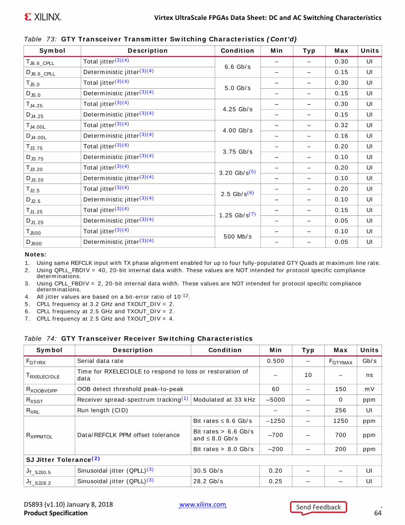
Virtex UltraScale FPGAs Data Sheet: DC and AC Switching Characteristics
DS893 (v1.10) January 8, 2018 www.xilinx.comProduct Specification 64
TJ6.6_CPLL Total jitter(3)(4)6.6 Gb/s
– – 0.30 UI
DJ6.6_CPLL Deterministic jitter(3)(4) – – 0.15 UI
TJ5.0 Total jitter(3)(4)5.0 Gb/s
– – 0.30 UI
DJ5.0 Deterministic jitter(3)(4) – – 0.15 UI
TJ4.25 Total jitter(3)(4)4.25 Gb/s
– – 0.30 UI
DJ4.25 Deterministic jitter(3)(4) – – 0.15 UI
TJ4.00L Total jitter(3)(4)4.00 Gb/s
– – 0.32 UI
DJ4.00L Deterministic jitter(3)(4) – – 0.16 UI
TJ3.75 Total jitter(3)(4)3.75 Gb/s
– – 0.20 UI
DJ3.75 Deterministic jitter(3)(4) – – 0.10 UI
TJ3.20 Total jitter(3)(4)3.20 Gb/s(5)
– – 0.20 UI
DJ3.20 Deterministic jitter(3)(4) – – 0.10 UI
TJ2.5 Total jitter(3)(4)2.5 Gb/s(6)
– – 0.20 UI
DJ2.5 Deterministic jitter(3)(4) – – 0.10 UI
TJ1.25 Total jitter(3)(4)1.25 Gb/s(7)
– – 0.15 UI
DJ1.25 Deterministic jitter(3)(4) – – 0.05 UI
TJ500 Total jitter(3)(4)500 Mb/s
– – 0.10 UI
DJ500 Deterministic jitter(3)(4) – – 0.05 UI
Notes: 1. Using same REFCLK input with TX phase alignment enabled for up to four fully-populated GTY Quads at maximum line rate.2. Using QPLL_FBDIV = 40, 20-bit internal data width. These values are NOT intended for protocol specific compliance
determinations.3. Using CPLL_FBDIV = 2, 20-bit internal data width. These values are NOT intended for protocol specific compliance
determinations.4. All jitter values are based on a bit-error ratio of 10-12.5. CPLL frequency at 3.2 GHz and TXOUT_DIV = 2.6. CPLL frequency at 2.5 GHz and TXOUT_DIV = 2.7. CPLL frequency at 2.5 GHz and TXOUT_DIV = 4.
Table 74: GTY Transceiver Receiver Switching Characteristics
Symbol Description Condition Min Typ Max UnitsFGTYRX Serial data rate 0.500 – FGTYMAX Gb/s
TRXELECIDLETime for RXELECIDLE to respond to loss or restoration of data – 10 – ns
RXOOBVDPP OOB detect threshold peak-to-peak 60 – 150 mV
RXSST Receiver spread-spectrum tracking(1) Modulated at 33 kHz –5000 – 0 ppm
RXRL Run length (CID) – – 256 UI
RXPPMTOL Data/REFCLK PPM offset tolerance
Bit rates ≤ 6.6 Gb/s –1250 – 1250 ppm
Bit rates > 6.6 Gb/s and ≤ 8.0 Gb/s –700 – 700 ppm
Bit rates > 8.0 Gb/s –200 – 200 ppm
SJ Jitter Tolerance(2)
JT_SJ30.5 Sinusoidal jitter (QPLL)(3) 30.5 Gb/s 0.20 – – UI
JT_SJ28.2 Sinusoidal jitter (QPLL)(3) 28.2 Gb/s 0.25 – – UI
Table 73: GTY Transceiver Transmitter Switching Characteristics (Cont’d)
Symbol Description Condition Min Typ Max Units
Send Feedback

Virtex UltraScale FPGAs Data Sheet: DC and AC Switching Characteristics
DS893 (v1.10) January 8, 2018 www.xilinx.comProduct Specification 65
JT_SJ25.78 Sinusoidal jitter (QPLL)(3) 25.78 Gb/s 0.25 – – UI
JT_SJ16.375 Sinusoidal jitter (QPLL)(3) 16.375 Gb/s 0.30 – – UI
JT_SJ15 Sinusoidal jitter (QPLL)(3) 15.0 Gb/s 0.30 – – UI
JT_SJ14.1 Sinusoidal jitter (QPLL)(3) 14.1 Gb/s 0.30 – – UI
JT_SJ13.1 Sinusoidal jitter (QPLL)(3) 13.1 Gb/s 0.30 – – UI
JT_SJ12.5_QPLL Sinusoidal jitter (QPLL)(3) 12.5 Gb/s 0.30 – – UI
JT_SJ12.5_CPLL Sinusoidal jitter (QPLL)(3) 12.5 Gb/s 0.30 – – UI
JT_SJ11.3_QPLL Sinusoidal jitter (QPLL)(3) 11.3 Gb/s 0.30 – – UI
JT_SJ10.32_QPLL Sinusoidal jitter (QPLL)(3) 10.32 Gb/s 0.30 – – UI
JT_SJ10.32_CPLL Sinusoidal jitter (CPLL)(3) 10.32 Gb/s 0.30 – – UI
JT_SJ9.8 Sinusoidal jitter (QPLL)(3) 9.8 Gb/s 0.30 – – UI
JT_SJ8.0_QPLL Sinusoidal jitter (QPLL)(3) 8.0 Gb/s 0.44 – – UI
JT_SJ8.0_CPLL Sinusoidal jitter (CPLL)(3) 8.0 Gb/s 0.42 – – UI
JT_SJ6.6_CPLL Sinusoidal jitter (CPLL)(3) 6.6 Gb/s 0.44 – – UI
JT_SJ5.0 Sinusoidal jitter (CPLL)(3) 5.0 Gb/s 0.44 – – UI
JT_SJ4.25 Sinusoidal jitter (CPLL)(3) 4.25 Gb/s 0.44 – – UI
JT_SJ4.00L Sinusoidal jitter (CPLL)(3) 4.0 Gb/s 0.45 – – UI
JT_SJ3.75 Sinusoidal jitter (CPLL)(3) 3.75 Gb/s 0.45 – – UI
JT_SJ3.20 Sinusoidal jitter (CPLL)(3) 3.2 Gb/s(4) 0.45 – – UI
JT_SJ2.5 Sinusoidal jitter (CPLL)(3) 2.5 Gb/s(5) 0.50 – – UI
JT_SJ1.25 Sinusoidal jitter (CPLL)(3) 1.25 Gb/s(6) 0.50 – – UI
JT_SJ500 Sinusoidal jitter (CPLL)(3) 500 Mb/s 0.50 – – UI
SJ Jitter Tolerance with Stressed Eye(2)
JT_TJSE3.2 Total jitter with stressed eye(7)3.2 Gb/s 0.7 – – UI
JT_TJSE6.6 6.6 Gb/s 0.7 – – UI
JT_SJSE3.2 Sinusoidal jitter with stressed eye(7)3.2 Gb/s 0.7 – – UI
JT_SJSE6.6 6.6 Gb/s 0.7 – – UI
Notes: 1. Using RXOUT_DIV = 1, 2, and 4.2. All jitter values are based on a bit error ratio of 10–12.3. The frequency of the injected sinusoidal jitter is 80 MHz.4. CPLL frequency at 3.2 GHz and RXOUT_DIV = 2.5. CPLL frequency at 2.5 GHz and RXOUT_DIV = 2.6. CPLL frequency at 2.5 GHz and RXOUT_DIV = 4.7. Composite jitter with RX equalizer enabled. DFE disabled.
Table 74: GTY Transceiver Receiver Switching Characteristics (Cont’d)
Symbol Description Condition Min Typ Max Units
Send Feedback
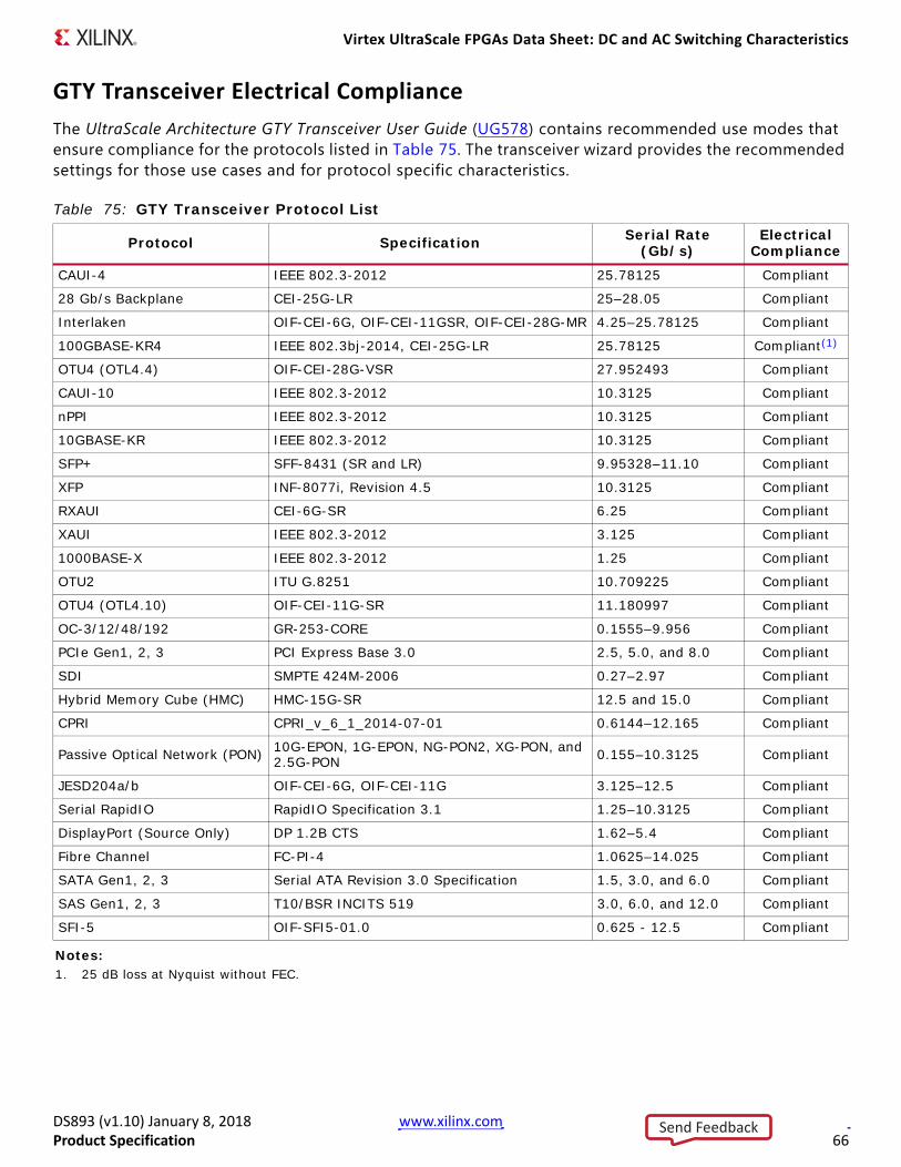
Virtex UltraScale FPGAs Data Sheet: DC and AC Switching Characteristics
DS893 (v1.10) January 8, 2018 www.xilinx.comProduct Specification 66
GTY Transceiver Electrical ComplianceThe UltraScale Architecture GTY Transceiver User Guide (UG578) contains recommended use modes that ensure compliance for the protocols listed in Table 75. The transceiver wizard provides the recommended settings for those use cases and for protocol specific characteristics.
Table 75: GTY Transceiver Protocol List
Protocol Specification Serial Rate (Gb/s)
Electrical Compliance
CAUI-4 IEEE 802.3-2012 25.78125 Compliant
28 Gb/s Backplane CEI-25G-LR 25–28.05 Compliant
Interlaken OIF-CEI-6G, OIF-CEI-11GSR, OIF-CEI-28G-MR 4.25–25.78125 Compliant
100GBASE-KR4 IEEE 802.3bj-2014, CEI-25G-LR 25.78125 Compliant(1)
OTU4 (OTL4.4) OIF-CEI-28G-VSR 27.952493 Compliant
CAUI-10 IEEE 802.3-2012 10.3125 Compliant
nPPI IEEE 802.3-2012 10.3125 Compliant
10GBASE-KR IEEE 802.3-2012 10.3125 Compliant
SFP+ SFF-8431 (SR and LR) 9.95328–11.10 Compliant
XFP INF-8077i, Revision 4.5 10.3125 Compliant
RXAUI CEI-6G-SR 6.25 Compliant
XAUI IEEE 802.3-2012 3.125 Compliant
1000BASE-X IEEE 802.3-2012 1.25 Compliant
OTU2 ITU G.8251 10.709225 Compliant
OTU4 (OTL4.10) OIF-CEI-11G-SR 11.180997 Compliant
OC-3/12/48/192 GR-253-CORE 0.1555–9.956 Compliant
PCIe Gen1, 2, 3 PCI Express Base 3.0 2.5, 5.0, and 8.0 Compliant
SDI SMPTE 424M-2006 0.27–2.97 Compliant
Hybrid Memory Cube (HMC) HMC-15G-SR 12.5 and 15.0 Compliant
CPRI CPRI_v_6_1_2014-07-01 0.6144–12.165 Compliant
Passive Optical Network (PON) 10G-EPON, 1G-EPON, NG-PON2, XG-PON, and 2.5G-PON 0.155–10.3125 Compliant
JESD204a/b OIF-CEI-6G, OIF-CEI-11G 3.125–12.5 Compliant
Serial RapidIO RapidIO Specification 3.1 1.25–10.3125 Compliant
DisplayPort (Source Only) DP 1.2B CTS 1.62–5.4 Compliant
Fibre Channel FC-PI-4 1.0625–14.025 Compliant
SATA Gen1, 2, 3 Serial ATA Revision 3.0 Specification 1.5, 3.0, and 6.0 Compliant
SAS Gen1, 2, 3 T10/BSR INCITS 519 3.0, 6.0, and 12.0 Compliant
SFI-5 OIF-SFI5-01.0 0.625 - 12.5 Compliant
Notes: 1. 25 dB loss at Nyquist without FEC.
Send Feedback
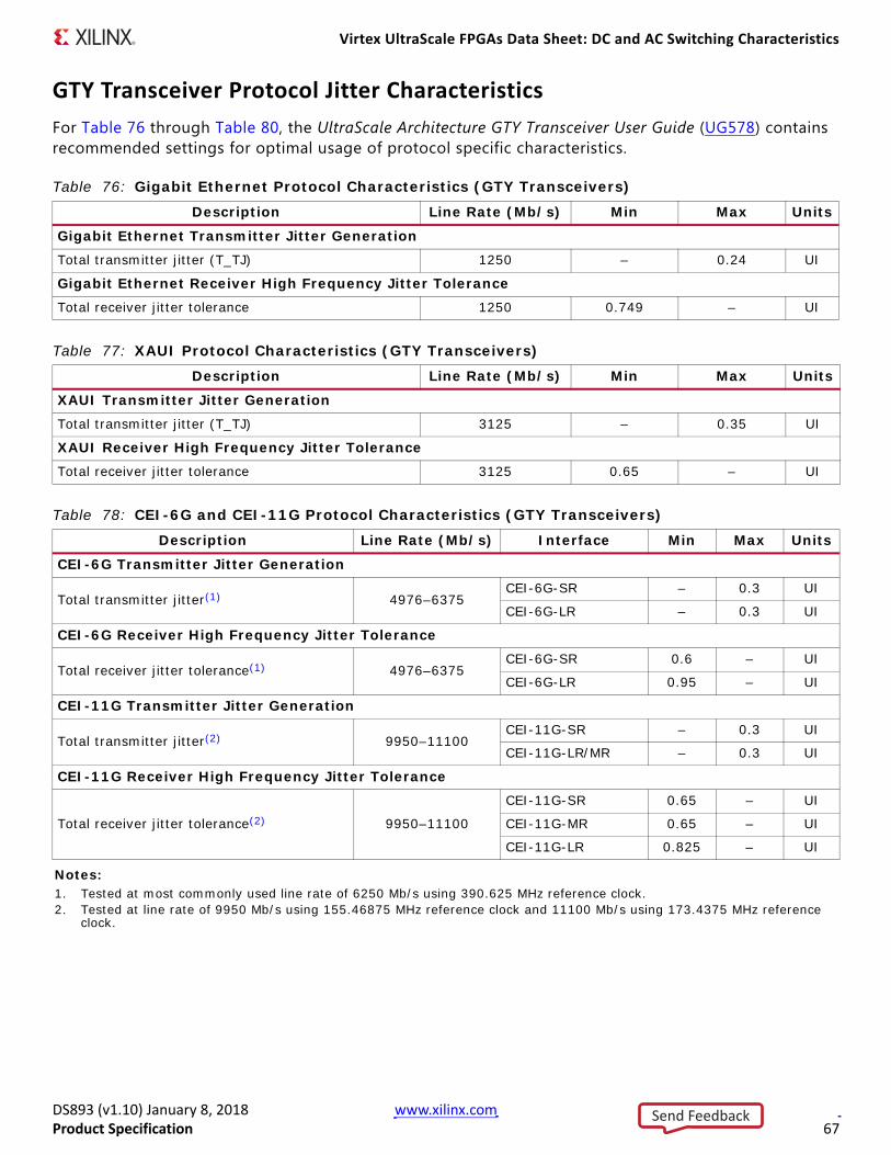
Virtex UltraScale FPGAs Data Sheet: DC and AC Switching Characteristics
DS893 (v1.10) January 8, 2018 www.xilinx.comProduct Specification 67
GTY Transceiver Protocol Jitter CharacteristicsFor Table 76 through Table 80, the UltraScale Architecture GTY Transceiver User Guide (UG578) contains recommended settings for optimal usage of protocol specific characteristics.
Table 76: Gigabit Ethernet Protocol Characteristics (GTY Transceivers)
Description Line Rate (Mb/s) Min Max Units
Gigabit Ethernet Transmitter Jitter GenerationTotal transmitter jitter (T_TJ) 1250 – 0.24 UI
Gigabit Ethernet Receiver High Frequency Jitter ToleranceTotal receiver jitter tolerance 1250 0.749 – UI
Table 77: XAUI Protocol Characteristics (GTY Transceivers)
Description Line Rate (Mb/s) Min Max Units
XAUI Transmitter Jitter GenerationTotal transmitter jitter (T_TJ) 3125 – 0.35 UI
XAUI Receiver High Frequency Jitter ToleranceTotal receiver jitter tolerance 3125 0.65 – UI
Table 78: CEI-6G and CEI-11G Protocol Characteristics (GTY Transceivers)
Description Line Rate (Mb/s) Interface Min Max Units
CEI-6G Transmitter Jitter Generation
Total transmitter jitter(1) 4976–6375CEI-6G-SR – 0.3 UI
CEI-6G-LR – 0.3 UI
CEI-6G Receiver High Frequency Jitter Tolerance
Total receiver jitter tolerance(1) 4976–6375CEI-6G-SR 0.6 – UI
CEI-6G-LR 0.95 – UI
CEI-11G Transmitter Jitter Generation
Total transmitter jitter(2) 9950–11100CEI-11G-SR – 0.3 UI
CEI-11G-LR/MR – 0.3 UI
CEI-11G Receiver High Frequency Jitter Tolerance
Total receiver jitter tolerance(2) 9950–11100
CEI-11G-SR 0.65 – UI
CEI-11G-MR 0.65 – UI
CEI-11G-LR 0.825 – UI
Notes: 1. Tested at most commonly used line rate of 6250 Mb/s using 390.625 MHz reference clock.2. Tested at line rate of 9950 Mb/s using 155.46875 MHz reference clock and 11100 Mb/s using 173.4375 MHz reference
clock.
Send Feedback
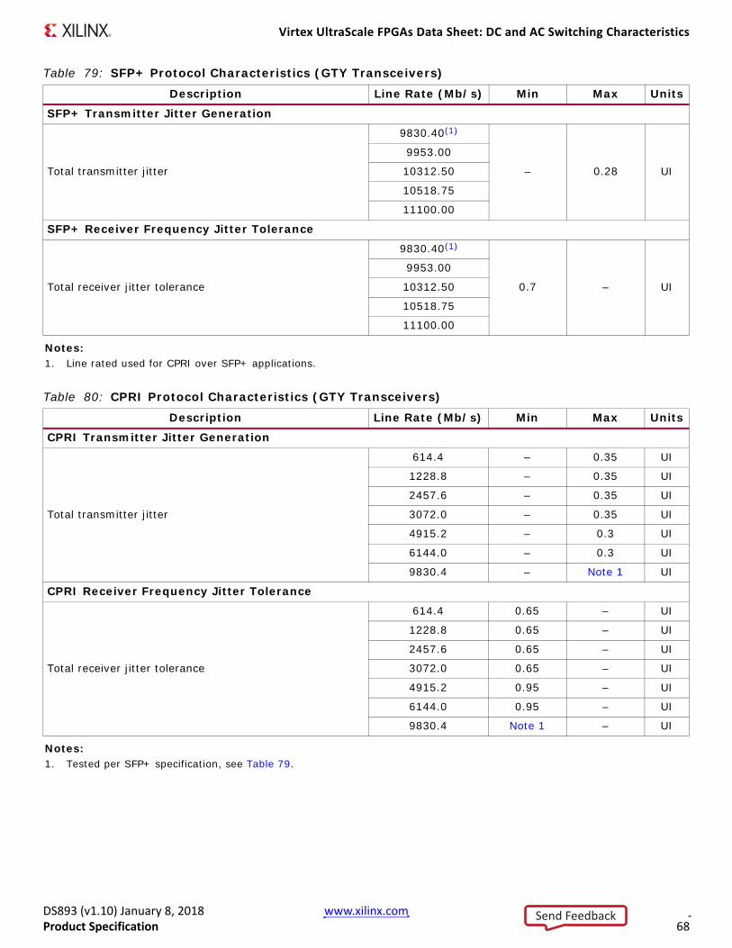
Virtex UltraScale FPGAs Data Sheet: DC and AC Switching Characteristics
DS893 (v1.10) January 8, 2018 www.xilinx.comProduct Specification 68
Table 79: SFP+ Protocol Characteristics (GTY Transceivers)
Description Line Rate (Mb/s) Min Max Units
SFP+ Transmitter Jitter Generation
Total transmitter jitter
9830.40(1)
– 0.28 UI
9953.00
10312.50
10518.75
11100.00
SFP+ Receiver Frequency Jitter Tolerance
Total receiver jitter tolerance
9830.40(1)
0.7 – UI
9953.00
10312.50
10518.75
11100.00
Notes: 1. Line rated used for CPRI over SFP+ applications.
Table 80: CPRI Protocol Characteristics (GTY Transceivers)
Description Line Rate (Mb/s) Min Max Units
CPRI Transmitter Jitter Generation
Total transmitter jitter
614.4 – 0.35 UI
1228.8 – 0.35 UI
2457.6 – 0.35 UI
3072.0 – 0.35 UI
4915.2 – 0.3 UI
6144.0 – 0.3 UI
9830.4 – Note 1 UI
CPRI Receiver Frequency Jitter Tolerance
Total receiver jitter tolerance
614.4 0.65 – UI
1228.8 0.65 – UI
2457.6 0.65 – UI
3072.0 0.65 – UI
4915.2 0.95 – UI
6144.0 0.95 – UI
9830.4 Note 1 – UI
Notes: 1. Tested per SFP+ specification, see Table 79.
Send Feedback

Virtex UltraScale FPGAs Data Sheet: DC and AC Switching Characteristics
DS893 (v1.10) January 8, 2018 www.xilinx.comProduct Specification 69
Integrated Interface Block for InterlakenMore information and documentation on solutions using the integrated interface block for Interlaken can be found at UltraScale Interlaken. The UltraScale Architecture and Product Overview (DS890) lists the Virtex UltraScale FPGAs that include this block.
Integrated Interface Block for 100G Ethernet MAC and PCSMore information and documentation on solutions using the integrated 100 Gb/s Ethernet block can be found at UltraScale Integrated 100G Ethernet MAC/PCS.
Table 81: Maximum Performance for Interlaken Designs
Symbol Description
Speed Grades and VCCINT Operating VoltagesUnit
s1.0V 0.95V
-3 -1H -2 -1
FRX_SERDES_CLKReceive serializer/ deserializer clock 402.84 402.84 402.84 195.32 MHz
FTX_SERDES_CLKTransmit serializer/ deserializer clock 402.84 402.84 402.84 195.32 MHz
FDRP_CLK
Dynamic reconfigurationport clock
250.00 250.00 250.00 250.00 MHz
Min Max Min Max Min Max Min Max
FCORE_CLK Interlaken core clock300.00(1)
429.69300.00(1)
429.69300.00(1)
429.69 300.00 322.27 MHz412.50(2) 412.50(2) 412.50(2)
FLBUS_CLKInterlaken local bus clock 300.00 349.52 300.00 349.52 300.00 349.52 300.00 322.27 MHz
Notes: 1. The minimum value for CORE_CLK is 300 MHz for the 12 x 12.5G Interlaken configuration.2. The minimum value for CORE_CLK is 412.5 MHz for the 6 x 25.78125G Interlaken configuration. This 6 x 25.78125G
configuration is not supported in the lane logic-only mode.
Table 82: Maximum Performance for 100G Ethernet Designs
Symbol Description
Speed Grades and VCCINT Operating Voltages
Units1.0V 0.95V
-3 -1H -2 -1FTX_CLK Transmit clock 322.27 322.27 322.27 322.27 MHz
FRX_CLK Receive clock 322.27 322.27 322.27 322.27 MHz
FRX_SERDES_CLK Receive serializer/deserializer clock 322.27 322.27 322.27 322.27 MHz
FDRP_CLK Dynamic reconfiguration port clock 250.00 250.00 250.00 250.00 MHz
Send Feedback

Virtex UltraScale FPGAs Data Sheet: DC and AC Switching Characteristics
DS893 (v1.10) January 8, 2018 www.xilinx.comProduct Specification 70
Integrated Interface Block for PCI Express DesignsMore information and documentation on solutions for PCI Express designs can be found at PCI Express.
System Monitor Specifications
Table 83: Maximum Performance for PCI Express Designs
Symbol Description
Speed Grades and VCCINT Operating Voltages
Units1.0V 0.95V
-3 -1H -2 -1FPIPECLK Pipe clock maximum frequency 250.00 250.00 250.00 250.00 MHz
FCORECLK Core clock maximum frequency 500.00 500.00(1) 500.00 500.00(1) MHz
FUSERCLK User clock maximum frequency 250.00 250.00 250.00 250.00 MHz
FDRPCLK DRP clock maximum frequency 250.00 250.00 250.00 250.00 MHz
Notes: 1. PCI Express x8 Gen3 operation is supported in -2 and -3 speed grades. Refer to the UltraScale Architecture Gen3
Integrated Block for PCI Express v4.1 User Guide (PG156) for information regarding x8 Gen 3 operation in the -1 speed grade.
Table 84: SYSMON Specifications
Parameter Symbol Comments/Conditions Min Typ Max Units
VCCADC = 1.8V ±3%, VREFP = 1.25V, VREFN = 0V, ADCCLK = 5.2 MHz, Tj = –40°C to 100°C, typical values at Tj = 40°C
ADC Accuracy(1)
Resolution 10 – – Bits
Integral nonlinearity(2) INL – – ±2 LSBs
Differential nonlinearity DNL No missing codes, guaranteed monotonic – – ±1 LSBs
Offset error Offset calibration enabled – – ±2 LSBs
Gain error – – ±0.4 %
Sample rate – – 0.2 MS/s
RMS code noiseExternal 1.25V reference – – 1 LSBs
On-chip reference – 1 – LSBs
ADC Accuracy at Extended TemperaturesResolution (Tj = –55°C to 125°C) 10 – – Bits
Integral nonlinearity INL (Tj = –55°C to 125°C) – – ±2LSBs
Differential nonlinearity DNL No missing codes, guaranteed monotonic. (Tj = –55°C to 125°C) – – ±1
Send Feedback
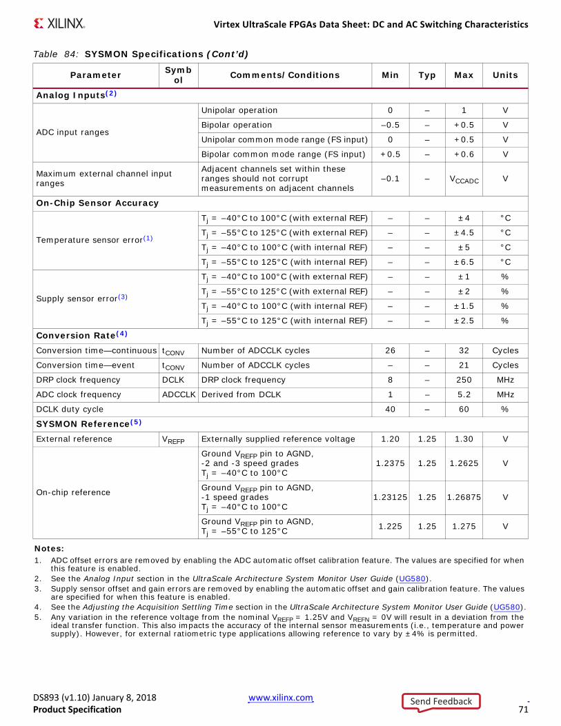
Virtex UltraScale FPGAs Data Sheet: DC and AC Switching Characteristics
DS893 (v1.10) January 8, 2018 www.xilinx.comProduct Specification 71
Analog Inputs(2)
ADC input ranges
Unipolar operation 0 – 1 V
Bipolar operation –0.5 – +0.5 V
Unipolar common mode range (FS input) 0 – +0.5 V
Bipolar common mode range (FS input) +0.5 – +0.6 V
Maximum external channel input ranges
Adjacent channels set within these ranges should not corrupt measurements on adjacent channels
–0.1 – VCCADC V
On-Chip Sensor Accuracy
Temperature sensor error(1)
Tj = –40°C to 100°C (with external REF) – – ±4 °C
Tj = –55°C to 125°C (with external REF) – – ±4.5 °C
Tj = –40°C to 100°C (with internal REF) – – ±5 °C
Tj = –55°C to 125°C (with internal REF) – – ±6.5 °C
Supply sensor error(3)
Tj = –40°C to 100°C (with external REF) – – ±1 %
Tj = –55°C to 125°C (with external REF) – – ±2 %
Tj = –40°C to 100°C (with internal REF) – – ±1.5 %
Tj = –55°C to 125°C (with internal REF) – – ±2.5 %
Conversion Rate(4)
Conversion time—continuous tCONV Number of ADCCLK cycles 26 – 32 Cycles
Conversion time—event tCONV Number of ADCCLK cycles – – 21 Cycles
DRP clock frequency DCLK DRP clock frequency 8 – 250 MHz
ADC clock frequency ADCCLK Derived from DCLK 1 – 5.2 MHz
DCLK duty cycle 40 – 60 %
SYSMON Reference(5)
External reference VREFP Externally supplied reference voltage 1.20 1.25 1.30 V
On-chip reference
Ground VREFP pin to AGND, -2 and -3 speed gradesTj = –40°C to 100°C
1.2375 1.25 1.2625 V
Ground VREFP pin to AGND, -1 speed gradesTj = –40°C to 100°C
1.23125 1.25 1.26875 V
Ground VREFP pin to AGND, Tj = –55°C to 125°C 1.225 1.25 1.275 V
Notes: 1. ADC offset errors are removed by enabling the ADC automatic offset calibration feature. The values are specified for when
this feature is enabled.2. See the Analog Input section in the UltraScale Architecture System Monitor User Guide (UG580).3. Supply sensor offset and gain errors are removed by enabling the automatic offset and gain calibration feature. The values
are specified for when this feature is enabled.4. See the Adjusting the Acquisition Settling Time section in the UltraScale Architecture System Monitor User Guide (UG580).5. Any variation in the reference voltage from the nominal VREFP = 1.25V and VREFN = 0V will result in a deviation from the
ideal transfer function. This also impacts the accuracy of the internal sensor measurements (i.e., temperature and power supply). However, for external ratiometric type applications allowing reference to vary by ±4% is permitted.
Table 84: SYSMON Specifications (Cont’d)
Parameter Symbol Comments/Conditions Min Typ Max Units
Send Feedback
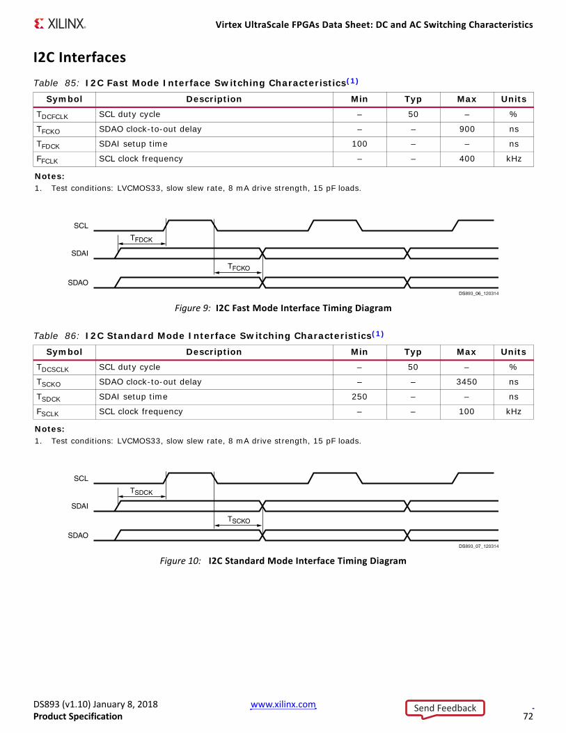
Virtex UltraScale FPGAs Data Sheet: DC and AC Switching Characteristics
DS893 (v1.10) January 8, 2018 www.xilinx.comProduct Specification 72
I2C InterfacesTable 85: I2C Fast Mode Interface Switching Characteristics(1)
Symbol Description Min Typ Max UnitsTDCFCLK SCL duty cycle – 50 – %
TFCKO SDAO clock-to-out delay – – 900 ns
TFDCK SDAI setup time 100 – – ns
FFCLK SCL clock frequency – – 400 kHz
Notes: 1. Test conditions: LVCMOS33, slow slew rate, 8 mA drive strength, 15 pF loads.
X-Ref Target - Figure 9
Figure 9: I2C Fast Mode Interface Timing Diagram
Table 86: I2C Standard Mode Interface Switching Characteristics(1)
Symbol Description Min Typ Max UnitsTDCSCLK SCL duty cycle – 50 – %
TSCKO SDAO clock-to-out delay – – 3450 ns
TSDCK SDAI setup time 250 – – ns
FSCLK SCL clock frequency – – 100 kHz
Notes: 1. Test conditions: LVCMOS33, slow slew rate, 8 mA drive strength, 15 pF loads.
X-Ref Target - Figure 10
Figure 10: I2C Standard Mode Interface Timing Diagram
TFCKO
TFDCK
DS893_06_120314
SCL
SDAI
SDAO
TSCKO
TSDCK
DS893_07_120314
SCL
SDAI
SDAO
Send Feedback

Virtex UltraScale FPGAs Data Sheet: DC and AC Switching Characteristics
DS893 (v1.10) January 8, 2018 www.xilinx.comProduct Specification 73
Configuration Switching CharacteristicsTable 87: Configuration Switching Characteristics
Symbol Description
Speed Grades and VCCINT Operating Voltages
Units1.0V 0.95V
-3 -1H -2 -1
Power-up Timing CharacteristicsTPL Program latency 7.5 7.5 7.5 7.5 ms, Max
TPOR
Power-on reset(40 ms maximum ramp rate time)
57 57 57 57 ms, Max
0 0 0 0 ms, Min
Power-on reset with POR override (2 ms maximum ramp rate time)
15 15 15 15 ms, Max
5 5 5 5 ms, Min
TPROGRAM Program pulse width 250 250 250 250 ns, Min
CCLK Output (Master Mode)TICCK Master CCLK output delay from INIT_B 150 150 150 150 ns, Min
TMCCKL Master CCLK clock Low time duty cycle 40/60 40/60 40/60 40/60 %, Min/Max
TMCCKH Master CCLK clock High time duty cycle 40/60 40/60 40/60 40/60 %, Min/Max
FMCCKMaster CCLK frequency
SPI x2/x4/x8BPI x8, x16 150 150 150 150 MHz, Max
SPI x1 and serial SLR-based devices 100 100 100 100 MHz, Max
SPI x1 and serial all other devices 150 150 150 150 MHz, Max
SelectMAP 125 125 125 125 MHz, Max
FMCCK_STARTMaster CCLK frequency at start of configuration 3 3 3 3 MHz, Typ
FMCCKTOLFrequency tolerance, master mode with respect to nominal CCLK ±35 ±35 ±35 ±35 %, Max
CCLK Input (Slave Modes)TSCCKL Slave CCLK clock minimum Low time 2.5 2.5 2.5 2.5 ns, Min
TSCCKH Slave CCLK clock minimum High time 2.5 2.5 2.5 2.5 ns, Min
FSCCK Slave CCLK frequency
Serial SLR-based devices 100 100 100 100 MHz, Max
Serial all other devices 150 150 150 150 MHz, Max
SelectMAP 125 125 125 125 MHz, Max
Send Feedback
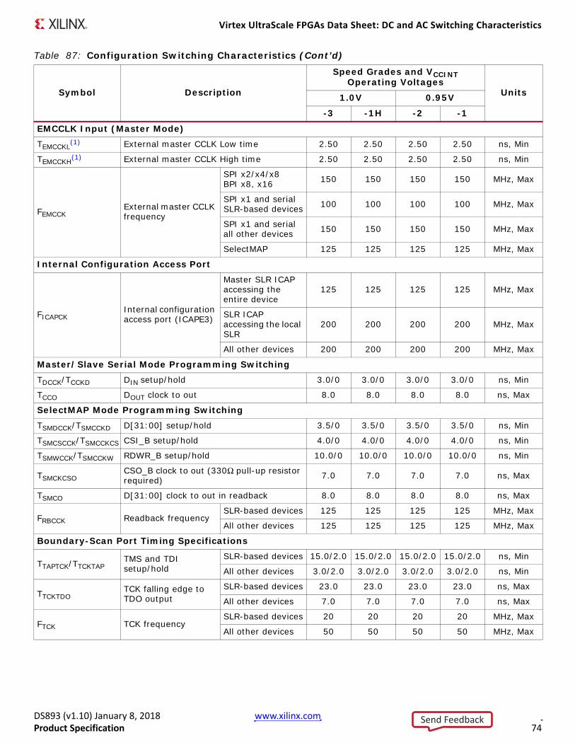
Virtex UltraScale FPGAs Data Sheet: DC and AC Switching Characteristics
DS893 (v1.10) January 8, 2018 www.xilinx.comProduct Specification 74
EMCCLK Input (Master Mode)TEMCCKL
(1) External master CCLK Low time 2.50 2.50 2.50 2.50 ns, Min
TEMCCKH(1) External master CCLK High time 2.50 2.50 2.50 2.50 ns, Min
FEMCCKExternal master CCLK frequency
SPI x2/x4/x8BPI x8, x16 150 150 150 150 MHz, Max
SPI x1 and serialSLR-based devices 100 100 100 100 MHz, Max
SPI x1 and serialall other devices 150 150 150 150 MHz, Max
SelectMAP 125 125 125 125 MHz, Max
Internal Configuration Access Port
FICAPCKInternal configuration access port (ICAPE3)
Master SLR ICAP accessing the entire device
125 125 125 125 MHz, Max
SLR ICAP accessing the local SLR
200 200 200 200 MHz, Max
All other devices 200 200 200 200 MHz, Max
Master/Slave Serial Mode Programming SwitchingTDCCK/TCCKD DIN setup/hold 3.0/0 3.0/0 3.0/0 3.0/0 ns, Min
TCCO DOUT clock to out 8.0 8.0 8.0 8.0 ns, Max
SelectMAP Mode Programming SwitchingTSMDCCK/TSMCCKD D[31:00] setup/hold 3.5/0 3.5/0 3.5/0 3.5/0 ns, Min
TSMCSCCK/TSMCCKCS CSI_B setup/hold 4.0/0 4.0/0 4.0/0 4.0/0 ns, Min
TSMWCCK/TSMCCKW RDWR_B setup/hold 10.0/0 10.0/0 10.0/0 10.0/0 ns, Min
TSMCKCSOCSO_B clock to out (330Ω pull-up resistor required) 7.0 7.0 7.0 7.0 ns, Max
TSMCO D[31:00] clock to out in readback 8.0 8.0 8.0 8.0 ns, Max
FRBCCK Readback frequencySLR-based devices 125 125 125 125 MHz, Max
All other devices 125 125 125 125 MHz, Max
Boundary-Scan Port Timing Specifications
TTAPTCK/TTCKTAPTMS and TDI setup/hold
SLR-based devices 15.0/2.0 15.0/2.0 15.0/2.0 15.0/2.0 ns, Min
All other devices 3.0/2.0 3.0/2.0 3.0/2.0 3.0/2.0 ns, Min
TTCKTDOTCK falling edge to TDO output
SLR-based devices 23.0 23.0 23.0 23.0 ns, Max
All other devices 7.0 7.0 7.0 7.0 ns, Max
FTCK TCK frequencySLR-based devices 20 20 20 20 MHz, Max
All other devices 50 50 50 50 MHz, Max
Table 87: Configuration Switching Characteristics (Cont’d)
Symbol Description
Speed Grades and VCCINT Operating Voltages
Units1.0V 0.95V
-3 -1H -2 -1
Send Feedback

Virtex UltraScale FPGAs Data Sheet: DC and AC Switching Characteristics
DS893 (v1.10) January 8, 2018 www.xilinx.comProduct Specification 75
BPI Master Flash Mode Programming Switching
TBPICCOA[28:00], RS[1:0], FCS_B, FOE_B, FWE_B, ADV_B clock to out 10.0 10.0 10.0 10.0 ns, Max
TBPIDCC/TBPICCD D[15:00] setup/hold 3.5/0 3.5/0 3.5/0 3.5/0 ns, Min
SPI Master Flash Mode Programming SwitchingTSPIDCC/TSPICCD D[03:00] setup/hold 3.0/0 3.0/0 3.0/0 3.0/0 ns, Min
TSPIDCC/TSPICCD D[07:04] setup/hold 3.5/0 3.5/0 3.5/0 3.5/0 ns, Min
TSPICCM MOSI clock to out 8.0 8.0 8.0 8.0 ns, Max
TSPICCM2 D[04] clock to out 10.0 10.0 10.0 10.0 ns, Max
TSPICCFC FCS_B clock to out 8.0 8.0 8.0 8.0 ns, Max
TSPICCFC2 FCS2_B clock to out 10.0 10.0 10.0 10.0 ns, Max
DNA Port SwitchingFDNACK DNA port frequency 200 200 200 200 MHz, Max
STARTUPE3 Ports
TUSRCCLKOSTARTUPE3 USRCCLKO input port to CCLK pin output delay
1.00/6.00
1.00/6.70
1.00/6.70
1.00/7.50 ns, Min/Max
TDODO[3:0] ports to D03-D00 pins output delay
1.00/6.70
1.00/7.70
1.00/7.70
1.00/8.40 ns, Min/Max
TDTSDTS[3:0] ports to D03-D00 pins 3-state delays
1.00/7.30
1.00/8.30
1.00/8.30
1.00/9.00 ns, Min/Max
TFCSBO FCSBO port to FCS_B pin output delay 1.00/6.90
1.00/8.00
1.00/8.00
1.00/8.60 ns, Min/Max
TFCSBTS FCSBTS port to FCS_B pin 3-state delay 1.00/6.90
1.00/8.00
1.00/8.00
1.00/8.60 ns, Min/Max
TUSRDONEO USRDONEO port to DONE pin output delay 1.00/8.50
1.00/9.60
1.00/9.60
1.00/10.40 ns, Min/Max
TUSRDONETSUSRDONETS port to DONE pin 3-state delay
1.00/8.50
1.00/9.60
1.00/9.60
1.00/10.40 ns, Min/Max
TDI D03-D00 pins to DI[3:0] ports input delay 0.5/2.6
0.5/3.1
0.5/3.1
0.5/3.5 ns, Min/Max
FCFGMCLK STARTUPE3 CFGMCLK output frequency 50 50 50 50 MHz, Typ
FCFGMCLKTOLSTARTUPE3 CFGMCLK output frequency tolerance ±15 ±15 ±15 ±15 %, Max
Startup Timing
TDCI_MATCH
Specifies a stall in the startup cycle until the digitally controlled impedance (DCI) match signals are asserted.
4 4 4 4 ms, Max
Notes: 1. When the CCLK is sourced from the EMCCLK pin with a divide-by-one setting, the external EMCCLK must meet these low
time and high time requirements.
Table 87: Configuration Switching Characteristics (Cont’d)
Symbol Description
Speed Grades and VCCINT Operating Voltages
Units1.0V 0.95V
-3 -1H -2 -1
Send Feedback
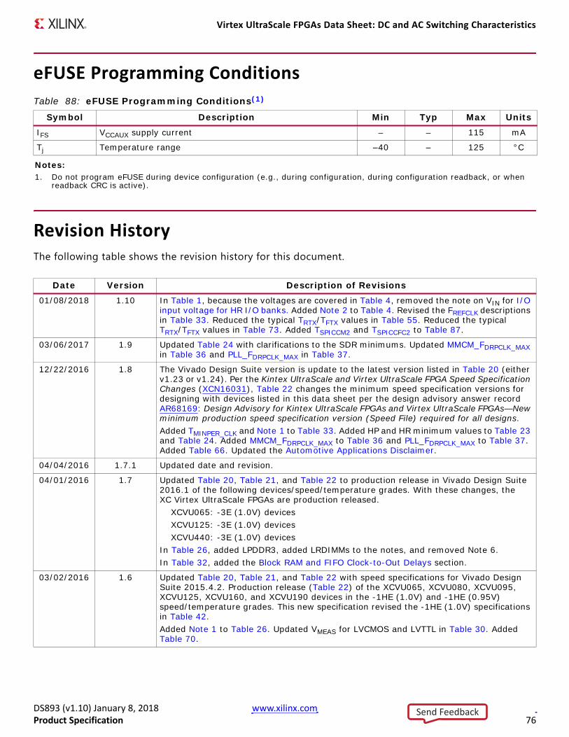
Virtex UltraScale FPGAs Data Sheet: DC and AC Switching Characteristics
DS893 (v1.10) January 8, 2018 www.xilinx.comProduct Specification 76
eFUSE Programming Conditions
Revision HistoryThe following table shows the revision history for this document.
Table 88: eFUSE Programming Conditions(1)
Symbol Description Min Typ Max UnitsIFS VCCAUX supply current – – 115 mA
Tj Temperature range –40 – 125 °C
Notes: 1. Do not program eFUSE during device configuration (e.g., during configuration, during configuration readback, or when
readback CRC is active).
Date Version Description of Revisions01/08/2018 1.10 In Table 1, because the voltages are covered in Table 4, removed the note on VIN for I/O
input voltage for HR I/O banks. Added Note 2 to Table 4. Revised the FREFCLK descriptions in Table 33. Reduced the typical TRTX/TFTX values in Table 55. Reduced the typical TRTX/TFTX values in Table 73. Added TSPICCM2 and TSPICCFC2 to Table 87.
03/06/2017 1.9 Updated Table 24 with clarifications to the SDR minimums. Updated MMCM_FDRPCLK_MAX in Table 36 and PLL_FDRPCLK_MAX in Table 37.
12/22/2016 1.8 The Vivado Design Suite version is update to the latest version listed in Table 20 (either v1.23 or v1.24). Per the Kintex UltraScale and Virtex UltraScale FPGA Speed Specification Changes (XCN16031), Table 22 changes the minimum speed specification versions for designing with devices listed in this data sheet per the design advisory answer record AR68169: Design Advisory for Kintex UltraScale FPGAs and Virtex UltraScale FPGAs—New minimum production speed specification version (Speed File) required for all designs.Added TMINPER_CLK and Note 1 to Table 33. Added HP and HR minimum values to Table 23 and Table 24. Added MMCM_FDRPCLK_MAX to Table 36 and PLL_FDRPCLK_MAX to Table 37. Added Table 66. Updated the Automotive Applications Disclaimer.
04/04/2016 1.7.1 Updated date and revision.
04/01/2016 1.7 Updated Table 20, Table 21, and Table 22 to production release in Vivado Design Suite 2016.1 of the following devices/speed/temperature grades. With these changes, the XC Virtex UltraScale FPGAs are production released.
XCVU065: -3E (1.0V) devicesXCVU125: -3E (1.0V) devicesXCVU440: -3E (1.0V) devices
In Table 26, added LPDDR3, added LRDIMMs to the notes, and removed Note 6.In Table 32, added the Block RAM and FIFO Clock-to-Out Delays section.
03/02/2016 1.6 Updated Table 20, Table 21, and Table 22 with speed specifications for Vivado Design Suite 2015.4.2. Production release (Table 22) of the XCVU065, XCVU080, XCVU095, XCVU125, XCVU160, and XCVU190 devices in the -1HE (1.0V) and -1HE (0.95V) speed/temperature grades. This new specification revised the -1HE (1.0V) specifications in Table 42.Added Note 1 to Table 26. Updated VMEAS for LVCMOS and LVTTL in Table 30. Added Table 70.
Send Feedback

Virtex UltraScale FPGAs Data Sheet: DC and AC Switching Characteristics
DS893 (v1.10) January 8, 2018 www.xilinx.comProduct Specification 77
12/16/2015 1.5 Updated the Power-On/Off Power Supply Sequencing section. Updated Table 20, Table 21, and Table 22 with speed specifications for Vivado Design Suite 2015.4.1 v1.20 where applicable.Production release (Table 22) of the XCVU065 and XCVU125 devices in the -2E/-2I (0.95V) and -1I (0.95V) speed/temperature grades.Revised the XCVU065 values in Table 42.
11/24/2015 1.4 Added the -1HE (1.0V and 0.95V) speed grade throughout.Revised the GTH or GTY Transceiver section in Table 2.Updated Table 20, Table 21, Table 22, Table 27, and Table 28 with speed specifications for Vivado Design Suite 2015.4 v1.19. Production release (Table 22) of the XCVU160 and XCVU190 devices in the -3 (1.0V), -2 (0.95V), and -1 (0.95V) speed/temperature grades and XCVU440 in the -2 and -1 speed/temperature grades.Updated Table 67 and expanded Table 72 with -1HE values.
10/12/2015 1.3 Updated description of ICCADC in Table 3.Updated the description in Power-On/Off Power Supply Sequencing.Updated Table 20, Table 21, Table 22, Table 27, and Table 28 with speed specifications for Vivado Design Suite 2015.3 v1.18. Production release (Table 22) of the XCVU095 and XCVU080 devices in the -3 (1.0V), -2 (0.95V), and -1 (0.95V) speed/temperature grades.Added protocols to Table 57. Updated VCMOUTDC in Table 64. Added data to Table 73 and Table 74.In Table 87, revised values for FSCCK, FEMCCK, FRBCCK, and FTCK and added the Startup Timing section.
07/27/2015 1.2 In Table 18 and Table 19 updated Note 2, Note 3, and Note 4.Updated Table 20 and Table 38 through Table 43 with speed specifications for Vivado Design Suite 2015.2 v1.16.Updated the STARTUPE3 Ports descriptions in Table 87. Updated Note 1 in Table 88.
05/29/2015 1.1 Entire data sheet is updated. Some of the highlights are noted in this revision history although it is not comprehensive.Updated Note 2 and Note 3 in Table 1 and Note 3, Note 4, and Note 6 in Table 2. Added data and Note 2 to Table 3. Updated Note 3 in Table 6. Revised the Power-On/Off Power Supply Sequencing section. Updated the descriptions in Table 8. Revised the VOCM maximum for MINI_LVDS_25 and RSDS_25 in Table 12. Revised the VICM specifications in Table 14. Removed rows from Table 16 and Table 17. Removed VOH and VOL rows, revised the VOCM maximum, and revised VICM in Table 18. Removed VOH and VOL rows and revised VICM in Table 19. Updated Table 20, Table 27, and Table 28 with speed specifications for Vivado Design Suite 2015.1 v1.15. Added Note 1 to Table 29.Added the section: I/O Standard Adjustment Measurement Methodology. Updated FREFCLK in Table 33. Revised MMCM_FINMAX and MMCM_TLOCKMAX in Table 36. Updated the descriptions and PLL_FINMAX in Table 37. Added a discussion on the data in the device pin-to-pin parameter tables on page 39 and page 41. Updated Table 44. Updated the package information in Table 45. Updated VCMOUTDC and added Note 2 in Table 46. Added Table 48 and Table 52. Updated both Table 55 and Table 56. Updated and combined the protocol characteristic sections into the GTH Transceiver Electrical Compliance section. Updated some of the maximum values for FGTYMAX, FGTYQRANGE1, and FGTYQRANGE2 in Table 67. Updated FRXIN2 (data width conditions for internal logic) in Table 72. Updated and combined the protocol characteristic sections into the GTY Transceiver Electrical Compliance section. Revised the values for FLBUS_CLK in Table 81. Revised FCORECLK and Note 1 in Table 83. Updated the On-Chip Sensor Accuracy, On-chip reference, and Note 5 in Table 84. In Table 87, added more speed specifications, updated TPOR, TPL, FMCCKTOL, and FRBCCK, added the STARTUPE3 Ports section, and added Note 1.
07/10/2014 1.0 Initial Xilinx release.
Date Version Description of Revisions
Send Feedback

Virtex UltraScale FPGAs Data Sheet: DC and AC Switching Characteristics
DS893 (v1.10) January 8, 2018 www.xilinx.comProduct Specification 78
Notice of DisclaimerThe information disclosed to you hereunder (the “Materials”) is provided solely for the selection and use of Xilinx products. To themaximum extent permitted by applicable law: (1) Materials are made available "AS IS" and with all faults, Xilinx hereby DISCLAIMSALL WARRANTIES AND CONDITIONS, EXPRESS, IMPLIED, OR STATUTORY, INCLUDING BUT NOT LIMITED TO WARRANTIES OFMERCHANTABILITY, NON-INFRINGEMENT, OR FITNESS FOR ANY PARTICULAR PURPOSE; and (2) Xilinx shall not be liable (whetherin contract or tort, including negligence, or under any other theory of liability) for any loss or damage of any kind or nature relatedto, arising under, or in connection with, the Materials (including your use of the Materials), including for any direct, indirect,special, incidental, or consequential loss or damage (including loss of data, profits, goodwill, or any type of loss or damagesuffered as a result of any action brought by a third party) even if such damage or loss was reasonably foreseeable or Xilinx hadbeen advised of the possibility of the same. Xilinx assumes no obligation to correct any errors contained in the Materials or tonotify you of updates to the Materials or to product specifications. You may not reproduce, modify, distribute, or publicly displaythe Materials without prior written consent. Certain products are subject to the terms and conditions of Xilinx’s limited warranty,please refer to Xilinx’s Terms of Sale which can be viewed at www.xilinx.com/legal.htm#tos; IP cores may be subject to warrantyand support terms contained in a license issued to you by Xilinx. Xilinx products are not designed or intended to be fail-safe orfor use in any application requiring fail-safe performance; you assume sole risk and liability for use of Xilinx products in suchcritical applications, please refer to Xilinx’s Terms of Sale which can be viewed at www.xilinx.com/legal.htm#tos.
Automotive Applications DisclaimerAUTOMOTIVE PRODUCTS (IDENTIFIED AS "XA" IN THE PART NUMBER) ARE NOT WARRANTED FOR USE IN THE DEPLOYMENT OFAIRBAGS OR FOR USE IN APPLICATIONS THAT AFFECT CONTROL OF A VEHICLE ("SAFETY APPLICATION") UNLESS THERE IS ASAFETY CONCEPT OR REDUNDANCY FEATURE CONSISTENT WITH THE ISO 26262 AUTOMOTIVE SAFETY STANDARD ("SAFETYDESIGN"). CUSTOMER SHALL, PRIOR TO USING OR DISTRIBUTING ANY SYSTEMS THAT INCORPORATE PRODUCTS, THOROUGHLYTEST SUCH SYSTEMS FOR SAFETY PURPOSES. USE OF PRODUCTS IN A SAFETY APPLICATION WITHOUT A SAFETY DESIGN IS FULLYAT THE RISK OF CUSTOMER, SUBJECT ONLY TO APPLICABLE LAWS AND REGULATIONS GOVERNING LIMITATIONS ON PRODUCTLIABILITY.
Send Feedback


![Developing Tamper-Resistant Designs with Zynq UltraScale+ ... · Developing Tamper Resistant Designs with UltraScale and UltraScale+ FPGAs (XAPP1098) [Ref6] provide a useful background](https://static.fdocuments.us/doc/165x107/5f0b3f187e708231d42f9162/developing-tamper-resistant-designs-with-zynq-ultrascale-developing-tamper.jpg)