Virtex-7 FPGA VC7222 Characterization Kit IBERT · Virtex-7 FPGA VC7222 Characterization Kit IBERT...
74
Virtex-7 FPGA VC7222 Characterization Kit IBERT Getting Started Guide Vivado Design Suite 2014.2 UG971 (v5.1) September 17, 2014
Transcript of Virtex-7 FPGA VC7222 Characterization Kit IBERT · Virtex-7 FPGA VC7222 Characterization Kit IBERT...

Virtex-7 FPGA VC7222 Characterization Kit IBERTGetting Started Guide
Vivado Design Suite 2014.2
UG971 (v5.1) September 17, 2014
VC7222 IBERT Getting Started Guide www.xilinx.com UG971 (v5.1) September 17, 2014
Notice of DisclaimerThe information disclosed to you hereunder (the “Materials”) is provided solely for the selection and use of Xilinx products. To the maximum extent permitted by applicable law: (1) Materials are made available "AS IS" and with all faults, Xilinx hereby DISCLAIMS ALL WARRANTIES AND CONDITIONS, EXPRESS, IMPLIED, OR STATUTORY, INCLUDING BUT NOT LIMITED TO WARRANTIES OF MERCHANTABILITY, NON-INFRINGEMENT, OR FITNESS FOR ANY PARTICULAR PURPOSE; and (2) Xilinx shall not be liable (whether in contract or tort, including negligence, or under any other theory of liability) for any loss or damage of any kind or nature related to, arising under, or in connection with, the Materials (including your use of the Materials), including for any direct, indirect, special, incidental, or consequential loss or damage (including loss of data, profits, goodwill, or any type of loss or damage suffered as a result of any action brought by a third party) even if such damage or loss was reasonably foreseeable or Xilinx had been advised of the possibility of the same. Xilinx assumes no obligation to correct any errors contained in the Materials or to notify you of updates to the Materials or to product specifications. You may not reproduce, modify, distribute, or publicly display the Materials without prior written consent. Certain products are subject to the terms and conditions of Xilinx’s limited warranty, please refer to Xilinx’s Terms of Sale which can be viewed at www.xilinx.com/legal.htm#tos; IP cores may be subject to warranty and support terms contained in a license issued to you by Xilinx. Xilinx products are not designed or intended to be fail-safe or for use in any application requiring fail-safe performance; you assume sole risk and liability for use of Xilinx products in such critical applications, please refer to Xilinx’s Terms of Sale which can be viewed at www.xilinx.com/legal.htm#tos.
© Copyright 2013–2014 Xilinx, Inc. Xilinx, the Xilinx logo, Artix, ISE, Kintex, Spartan, Virtex, Vivado, Zynq, and other designated brands included herein are trademarks of Xilinx in the United States and other countries. CPRI is a trademark of Siemens AG. PCI, PCI Express, PCIe, and PCI-X are trademarks of PCI-SIG and used under license. All other trademarks are the property of their respective owners.
Revision HistoryThe following table shows the revision history for this document.
Date Version Revision
09/20/2013 1.0 Initial Xilinx release.
09/24/2013 1.0.1 Updated the Notice of Disclaimer, page 2..
11/07/2013 2.0 Updated for Vivado® Design Suite 2013.3. Updated most figures in Chapter 1, VC7222 IBERT Getting Started Guide. Figure 1-31 and Figure 2-11 were renamed Design Sources File Hierarchy. Deleted Figures 2-12 and Figure 3-9, Synthesize Out-Of-Context Module. The name of the project ZIP file changed to rdf0297-vc7222-ibert-2013-3.zip. Replaced Figure 3-8, Set As Out Of Context Module with Design Sources File Hierarchy screen. Deleted Figure 3-12, Edit the Implementation Setting. Updated Appendix A, Additional Resources links.
01/22/2014 3.0 Updated for Vivado Design Suite 2013.4. Updated Figure 1-11, Figure 1-13, Figure 1-14, Figure 1-15, Figure 1-27, Figure 1-28, Figure 1-29, Figure 1-33, Figure 2-1, and Figure 3-5.
04/16/2014 4.0 Updated for Vivado Design Suite 2014.1. Updated 30 graphics in Chapters 1, 2, and 3. File lists changed under Extracting the Project Files. The ZIP project file name changed to rdf0297-vc7222-ibert-2014-2.zip. Launching the Vivado Design Suite Software was changed to Setting Up the Vivado Design Suite Software in the Running the GTH IBERT Demonstration and Running the GTZ IBERT Demonstration sections, and In Case of RX Bit Errors was added to both sections.
06/12/2014 5.0 Updated for Vivado Design Suite 2014.2. Updated Figure 1-10, Figure 1-11, Figure 1-19, Figure 1-20, Figure 1-23, Figure 1-27, Figure 1-30, Figure 1-33, Figure 2-1, Figure 2-4, Figure 2-8, Figure 2-11, Figure 2-14, Figure 2-16, Figure 3-2, through Figure 3-5, Figure 3-8, Figure 3-11. and Figure 3-13. Updated Viewing GTH Transceiver Operation and Viewing the GTZ Transceiver Operation.

UG971 (v5.1) September 17, 2014 www.xilinx.com VC7222 IBERT Getting Started Guide
09/17/2014 5.1 Changed cable quantity from two to one under Requirements, page 8. Added a note about cable quantity in Running the GTZ IBERT Demonstration, page 27. Updated clock connection information in GTZ Transceiver Clock Connection, page 30. Added a Caution regarding BullsEye cable use in Attach the GTZ Quad Connector, page 29. Added a note about the cable connection in Figure 1-24 and before Figure 1-33. Replaced Figure 3-3.
Date Version Revision

VC7222 IBERT Getting Started Guide www.xilinx.com UG971 (v5.1) September 17, 2014
VC7222 IBERT Getting Started Guide www.xilinx.com 5UG971 (v5.1) September 17, 2014
Table of Contents
Revision History . . . . . . . . . . . . . . . . . . . . . . . . . . . . . . . . . . . . . . . . . . . . . . . . . . . . . . . . . . . . . 2
Chapter 1: VC7222 IBERT Getting Started GuideOverview . . . . . . . . . . . . . . . . . . . . . . . . . . . . . . . . . . . . . . . . . . . . . . . . . . . . . . . . . . . . . . . . . . . . 7Requirements . . . . . . . . . . . . . . . . . . . . . . . . . . . . . . . . . . . . . . . . . . . . . . . . . . . . . . . . . . . . . . . . 8Setting Up the VC7222 Board for GTH and GTZ IBERT Testing. . . . . . . . . . . . . . . 8Extracting the Project Files . . . . . . . . . . . . . . . . . . . . . . . . . . . . . . . . . . . . . . . . . . . . . . . . . . . 9Running the GTH IBERT Demonstration . . . . . . . . . . . . . . . . . . . . . . . . . . . . . . . . . . . . 10
Connecting the GTH Transceivers and Reference Clocks . . . . . . . . . . . . . . . . . . . . . . . 10Attach the GTH Quad Connector . . . . . . . . . . . . . . . . . . . . . . . . . . . . . . . . . . . . . . . 12GTH Transceiver Clock Connections . . . . . . . . . . . . . . . . . . . . . . . . . . . . . . . . . . . . 13GTH TX/RX Loopback Connections . . . . . . . . . . . . . . . . . . . . . . . . . . . . . . . . . . . . 14
Configuring the FPGA. . . . . . . . . . . . . . . . . . . . . . . . . . . . . . . . . . . . . . . . . . . . . . . . . . . . . 15Setting Up the Vivado Design Suite Software . . . . . . . . . . . . . . . . . . . . . . . . . . . . . . . . . 17Starting the SuperClock-2 Module . . . . . . . . . . . . . . . . . . . . . . . . . . . . . . . . . . . . . . . . . . 20Viewing GTH Transceiver Operation . . . . . . . . . . . . . . . . . . . . . . . . . . . . . . . . . . . . . . . . 26
In Case of RX Bit Errors . . . . . . . . . . . . . . . . . . . . . . . . . . . . . . . . . . . . . . . . . . . . . . . 26Closing the IBERT Demonstration. . . . . . . . . . . . . . . . . . . . . . . . . . . . . . . . . . . . . . . . . . . 27
Running the GTZ IBERT Demonstration . . . . . . . . . . . . . . . . . . . . . . . . . . . . . . . . . . . . 27Connecting the GTZ Transceiver and Reference Clocks . . . . . . . . . . . . . . . . . . . . . . . . 27
Attach the GTZ Quad Connector . . . . . . . . . . . . . . . . . . . . . . . . . . . . . . . . . . . . . . . 29GTZ Transceiver Clock Connection . . . . . . . . . . . . . . . . . . . . . . . . . . . . . . . . . . . . . 30GTZ TX/RX Loopback Connections. . . . . . . . . . . . . . . . . . . . . . . . . . . . . . . . . . . . . 31
Configuring the FPGA. . . . . . . . . . . . . . . . . . . . . . . . . . . . . . . . . . . . . . . . . . . . . . . . . . . . . 33Setting up the Vivado Design Suite Software . . . . . . . . . . . . . . . . . . . . . . . . . . . . . . . . . 34Starting the SuperClock-2 Module . . . . . . . . . . . . . . . . . . . . . . . . . . . . . . . . . . . . . . . . . . 34Viewing the GTZ Transceiver Operation . . . . . . . . . . . . . . . . . . . . . . . . . . . . . . . . . . . . . 41
In Case of RX Bit Errors . . . . . . . . . . . . . . . . . . . . . . . . . . . . . . . . . . . . . . . . . . . . . . . 42Closing the IBERT Demonstration. . . . . . . . . . . . . . . . . . . . . . . . . . . . . . . . . . . . . . . . . . . 42
SuperClock-2 Frequency Table . . . . . . . . . . . . . . . . . . . . . . . . . . . . . . . . . . . . . . . . . . . . . . 42
Chapter 2: Creating the GTH IBERT Core
Chapter 3: Creating the GTZ IBERT Core
Appendix A: Additional ResourcesXilinx Resources . . . . . . . . . . . . . . . . . . . . . . . . . . . . . . . . . . . . . . . . . . . . . . . . . . . . . . . . . . . . 71Solution Centers . . . . . . . . . . . . . . . . . . . . . . . . . . . . . . . . . . . . . . . . . . . . . . . . . . . . . . . . . . . . 71References . . . . . . . . . . . . . . . . . . . . . . . . . . . . . . . . . . . . . . . . . . . . . . . . . . . . . . . . . . . . . . . . . . 71
Appendix B: Warranty
Send Feedback

6 www.xilinx.com VC7222 IBERT Getting Started GuideUG971 (v5.1) September 17, 2014
Send Feedback
VC7222 IBERT Getting Started Guide www.xilinx.com 7UG971 (v5.1) September 17, 2014
Chapter 1
VC7222 IBERT Getting Started Guide
OverviewThis document provides a procedure for setting up the Virtex®-7 FPGA VC7222 GTH and GTZ Transceiver Characterization Board to run the Integrated Bit Error Ratio Test (IBERT) demonstration using the Vivado® Design Suite. The designs required to run the IBERT demonstration are stored in the Secure Digital (SD) memory card provided with the VC7222 board. A copy of the designs can also be found at the Virtex-7 FPGA VC7222 Characterization Kit documentation website.
The VC7222 board is described in detail in Virtex-7 FPGA VC7222 GTH and GTZ Transceiver Characterization Board User Guide (UG965) [Ref 1].
The IBERT GTH demonstration operates one GTH Quad at a time. The procedure consists of:
• Setting Up the VC7222 Board for GTH and GTZ IBERT Testing, page 8
• Extracting the Project Files, page 9
• Connecting the GTH Transceivers and Reference Clocks, page 10
• Configuring the FPGA, page 15
• Setting Up the Vivado Design Suite Software, page 17
• Starting the SuperClock-2 Module, page 20
• Viewing GTH Transceiver Operation, page 26
• Closing the IBERT Demonstration, page 27
The IBERT GTZ demonstration operates 8 GTZ lanes using both Q300A and Q300B. The procedure consists of:
• Connecting the GTZ Transceiver and Reference Clocks, page 27
• Configuring the FPGA, page 33
• Setting up the Vivado Design Suite Software, page 34
• Starting the SuperClock-2 Module, page 20
• Viewing the GTZ Transceiver Operation, page 41
• Closing the IBERT Demonstration, page 42
Send Feedback

8 www.xilinx.com VC7222 IBERT Getting Started GuideUG971 (v5.1) September 17, 2014
Chapter 1: VC7222 IBERT Getting Started Guide
RequirementsThe hardware and software required to run the GTH and GTZ IBERT demonstration are listed here:
• Virtex-7 FPGA VC7222 GTH and GTZ Transceiver Characterization Board. The kit includes:
• One SD card containing the IBERT demonstration designs
• One Samtec BullsEye™ cable
• One skew-matched reference clock cable set
• Eight SMA female-to-female (F-F) adapters
• Six 50Ω SMA terminators
• GTH transceiver power supply module (installed on board)
• GTZ transceiver power supply module (installed on board)
• SuperClock-2 module, Rev 1.0 (installed on board)
• 12V DC power adapter
• USB cable, standard-A plug to Micro-B plug
• Host PC with:
• SD card reader
• USB ports
• Xilinx Vivado Design Suite 2014.2
The hardware and software required to rebuild the IBERT demonstration designs are:
• Xilinx Vivado Design Suite 2014.2
• Host PC with a version of the Windows operating system supported by the Xilinx Vivado Design Suite
Setting Up the VC7222 Board for GTH and GTZ IBERT TestingCaution! The VC7222 board can be damaged by electrostatic discharge (ESD). Follow standard ESD prevention measures when handling the board.
When the VC7222 board ships from the factory, it is already configured for the GTH IBERT demonstration described in this chapter. If the board has been re-configured, it must be returned to the default setup before running the IBERT demonstrations.
1. Move all jumpers and switches to their default positions. The default jumper and switch positions are listed in Virtex-7 FPGA VC7222 GTH and GTZ Transceiver Characterization Board User Guide (UG965) [Ref 1].
2. Install the GTH and GTZ transceiver power modules into connectors J29 – J102, and J5 and J71, respectively.
3. Install the SuperClock-2 module:
a. Align the three metal standoffs on the bottom side of the module with the three mounting holes in the SuperClock-2 module interface of the VC7222 board.
b. Using three 4-40 x 0.25 inch screws, firmly screw down the module from the bottom of the VC7222 board.
Send Feedback
VC7222 IBERT Getting Started Guide www.xilinx.com 9UG971 (v5.1) September 17, 2014
Extracting the Project Files
c. On the SuperClock-2 module, place a jumper across pins 2 - 3 (2V5) of the CONTROL VOLTAGE header, J18, and place another jumper across Si570 INH header J11.
d. Screw down a 50Ω SMA terminator onto each of the six unused Si5368 clock output SMA connectors: J7, J8, J12, J15, J16, and J17.
Extracting the Project FilesThe Vivado project files required to run the IBERT demonstration are located in rdf0297-vc7222-ibert-2014-2.zip on the SD card provided with the VC7222 board. These files are also available online at the Virtex-7 FPGA VC7222 Characterization Kit documentation website.
The ZIP file contains these files:
• BIT files
vc7222_ibert_q113_325.bit
vc7222_ibert_q114_325.bit
vc7222_ibert_q115_325.bit
vc7222_ibert_q213_325.bit
vc7222_ibert_q214_325.bit
vc7222_ibert_q215_325.bit
vc7222_ibert_q300_225.bit
vc7222_uarttest.bit
• Probe files
vc7222_ibert_q113_debug_nets.ltx
vc7222_ibert_q114_debug_nets.ltx
vc7222_ibert_q115_debug_nets.ltx
vc7222_ibert_q213_debug_nets.ltx
vc7222_ibert_q214_debug_nets.ltx
vc7222_ibert_q215_debug_nets.ltx
vc7222_ibert_q300_debug_nets.ltx
• Tcl scripts
add_scm2.tcl
setup_scm2_325_00_GTH.tcl
setup_scm2_225_00_GTZ.tcl
The Tcl scripts are used to help merge the IBERT and SuperClock-2 source code (described in Chapter 2, Creating the GTH IBERT Core and in Chapter 3, Creating the GTZ IBERT Core) and to set up the SuperClock-2 module (described in Starting the SuperClock-2 Module, page 20 in the GTH section and Starting the SuperClock-2 Module, page 34 in the GTZ section).
Send Feedback
10 www.xilinx.com VC7222 IBERT Getting Started GuideUG971 (v5.1) September 17, 2014
Chapter 1: VC7222 IBERT Getting Started Guide
To copy the files from the SD memory card:
1. Connect the SD card to the host computer.
2. Locate the file rdf0297-vc7222-ibert-2014-2.zip on the SD memory card.
3. Unzip the files to a working directory on the host computer.
Running the GTH IBERT DemonstrationThe GTH IBERT demonstration operates one GTH Quad at a time. This section describes how to test GTH Quad 115, while the remaining GTH Quads are tested following similar steps.
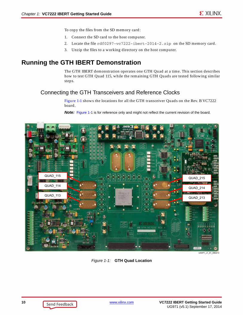
Connecting the GTH Transceivers and Reference ClocksFigure 1-1 shows the locations for all the GTH transceiver Quads on the Rev. B VC7222 board.
Note: Figure 1-1 is for reference only and might not reflect the current revision of the board.X-Ref Target - Figure 1-1
Figure 1-1: GTH Quad Location
Send Feedback
VC7222 IBERT Getting Started Guide www.xilinx.com 11UG971 (v5.1) September 17, 2014
Running the GTH IBERT Demonstration
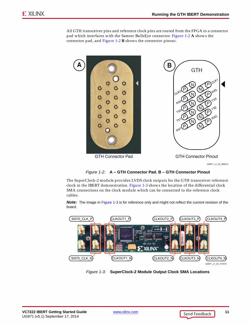
All GTH transceiver pins and reference clock pins are routed from the FPGA to a connector pad which interfaces with the Samtec BullsEye connector. Figure 1-2 A shows the connector pad, and Figure 1-2 B shows the connector pinout.
The SuperClock-2 module provides LVDS clock outputs for the GTH transceiver reference clock in the IBERT demonstration. Figure 1-3 shows the location of the differential clock SMA connections on the clock module which can be connected to the reference clock cables.
Note: The image in Figure 1-3 is for reference only and might not reflect the current revision of the board.
X-Ref Target - Figure 1-2
Figure 1-2: A – GTH Connector Pad. B – GTH Connector Pinout
X-Ref Target - Figure 1-3
Figure 1-3: SuperClock-2 Module Output Clock SMA Locations
Send Feedback

12 www.xilinx.com VC7222 IBERT Getting Started GuideUG971 (v5.1) September 17, 2014
Chapter 1: VC7222 IBERT Getting Started Guide
The four SMA pairs labeled CLKOUT provide LVDS clock outputs from the Si5368 clock multiplier/jitter attenuator device on the clock module. The SMA pair labeled Si570_CLK provides LVDS clock output from the Si570 programmable oscillator on the clock module.
Note: The Si570 oscillator does not support LVDS output on Rev. B and earlier revisions of the SuperClock-2 module.
For the GTH IBERT demonstration, the output clock frequencies are preset to 325.00 MHz. For more information regarding the SuperClock-2 module, see the HW-CLK-101-SCLK2 SuperClock-2 Module User Guide (UG770) [Ref 2].
Attach the GTH Quad Connector
Before connecting the BullsEye cable assembly to the board, firmly secure the blue elastomer seal provided with the cable assembly to the bottom of the connector housing, if it is not already inserted (see Figure 1-4).
Note: Figure 1-4 is for reference only and might not reflect the current version of the connector.X-Ref Target - Figure 1-4
Figure 1-4: BullsEye Connector with Elastomer Seal
Send Feedback

VC7222 IBERT Getting Started Guide www.xilinx.com 13UG971 (v5.1) September 17, 2014
Running the GTH IBERT Demonstration
Attach the Samtec BullsEye connector to the GTH Quad 115 (Figure 1-5), aligning the two indexing pins on the bottom of the connector with the guide holes on the board. Hold the connector flush with the board and fasten it by tightening the two captive screws.
GTH Transceiver Clock Connections
See Figure 1-2 to identify the P and N coax cables connected to the CLK0 reference clock inputs. Connect these cables to the SuperClock-2 module as follows:
• CLK0_P coax cable → SMA connector J5 (CLKOUT1_P) on the SuperClock-2 module
• CLK0_N coax cable → SMA connector J6 (CLKOUT1_N) on the SuperClock-2 module
Note: Any one of the five differential outputs from the SuperClock-2 module can be used to source the GTH reference clock. CLKOUT1_P and CLKOUT1_N are used here as an example.
X-Ref Target - Figure 1-5
Figure 1-5: BullsEye Connector Attached to GTH Quad 115
Send Feedback

14 www.xilinx.com VC7222 IBERT Getting Started GuideUG971 (v5.1) September 17, 2014
Chapter 1: VC7222 IBERT Getting Started Guide
GTH TX/RX Loopback Connections
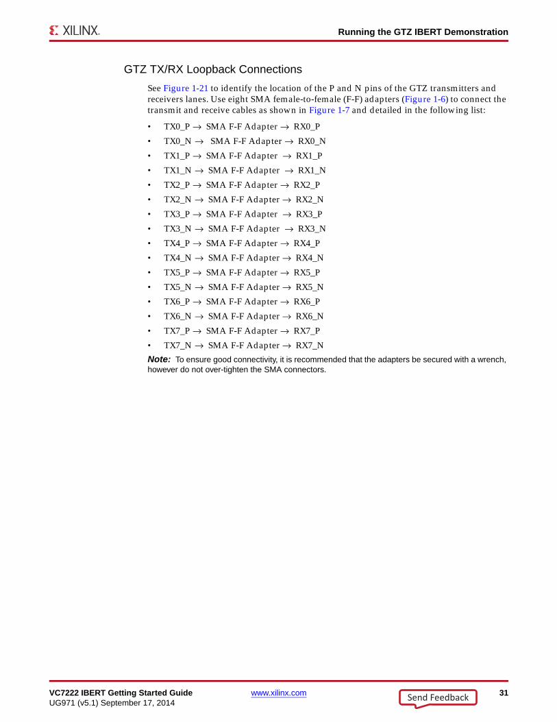
See Figure 1-2 to identify the P and N coax cables that are connected to the four receivers (RX0, RX1, RX2, and RX3) and the four transmitters (TX0, TX1, TX2, and TX3). Use eight SMA female-to-female (F-F) adapters (Figure 1-6) to connect the transmit and receive cables as shown in Figure 1-7 and detailed in the following list:
• TX0_P → SMA F-F Adapter → RX0_P
• TX0_N → SMA F-F Adapter → RX0_N
• TX1_P → SMA F-F Adapter → RX1_P
• TX1_N → SMA F-F Adapter → RX1_N
• TX2_P → SMA F-F Adapter → RX2_P
• TX2_N → SMA F-F Adapter → RX2_N
• TX3_P → SMA F-F Adapter → RX3_P
• TX3_N → SMA F-F Adapter → RX3_N
Note: To ensure good connectivity, it is recommended that the adapters be secured with a wrench, however do not over-tighten the SMAs.X-Ref Target - Figure 1-6
Figure 1-6: SMA F-F Adapter
X-Ref Target - Figure 1-7
Figure 1-7: TX-To-RX Loopback Connection Example
Send Feedback
VC7222 IBERT Getting Started Guide www.xilinx.com 15UG971 (v5.1) September 17, 2014
Running the GTH IBERT Demonstration
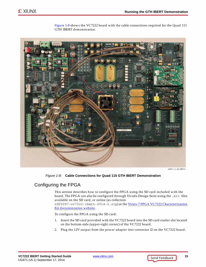
Figure 1-8 shows the VC7222 board with the cable connections required for the Quad 115 GTH IBERT demonstration.
Configuring the FPGAThis section describes how to configure the FPGA using the SD card included with the board. The FPGA can also be configured through Vivado Design Suite using the .bit files available on the SD card, or online (as collection rdf0297-vc7222-ibert-2014-2.zip) at the Virtex-7 FPGA VC7222 Characterization Kit documentation website.
To configure the FPGA using the SD card:
1. Insert the SD card provided with the VC7222 board into the SD card reader slot located on the bottom-side (upper-right corner) of the VC7222 board.
2. Plug the 12V output from the power adapter into connector J2 on the VC7222 board.
X-Ref Target - Figure 1-8
Figure 1-8: Cable Connections for Quad 115 GTH IBERT Demonstration
Send Feedback
16 www.xilinx.com VC7222 IBERT Getting Started GuideUG971 (v5.1) September 17, 2014
Chapter 1: VC7222 IBERT Getting Started Guide
3. Connect the host computer to the VC7222 board using a standard-A plug to Micro-B plug USB cable. The standard-A plug connects to a USB port on the host computer and the Micro-B plug connects to U57, the Digilent USB JTAG configuration port on the VC7222 board.
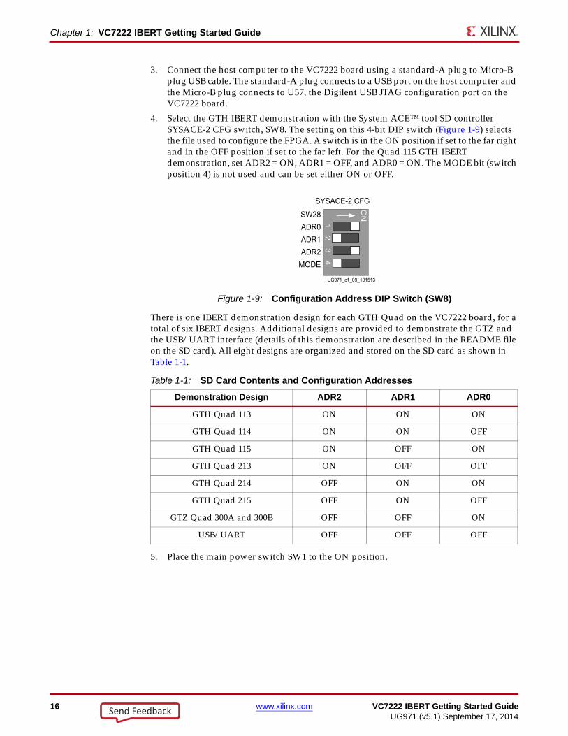
4. Select the GTH IBERT demonstration with the System ACE™ tool SD controller SYSACE-2 CFG switch, SW8. The setting on this 4-bit DIP switch (Figure 1-9) selects the file used to configure the FPGA. A switch is in the ON position if set to the far right and in the OFF position if set to the far left. For the Quad 115 GTH IBERT demonstration, set ADR2 = ON, ADR1 = OFF, and ADR0 = ON. The MODE bit (switch position 4) is not used and can be set either ON or OFF.
There is one IBERT demonstration design for each GTH Quad on the VC7222 board, for a total of six IBERT designs. Additional designs are provided to demonstrate the GTZ and the USB/UART interface (details of this demonstration are described in the README file on the SD card). All eight designs are organized and stored on the SD card as shown in Table 1-1.
5. Place the main power switch SW1 to the ON position.
X-Ref Target - Figure 1-9
Figure 1-9: Configuration Address DIP Switch (SW8)
Table 1-1: SD Card Contents and Configuration Addresses
Demonstration Design ADR2 ADR1 ADR0
GTH Quad 113 ON ON ON
GTH Quad 114 ON ON OFF
GTH Quad 115 ON OFF ON
GTH Quad 213 ON OFF OFF
GTH Quad 214 OFF ON ON
GTH Quad 215 OFF ON OFF
GTZ Quad 300A and 300B OFF OFF ON
USB/UART OFF OFF OFF
Send Feedback
VC7222 IBERT Getting Started Guide www.xilinx.com 17UG971 (v5.1) September 17, 2014
Running the GTH IBERT Demonstration
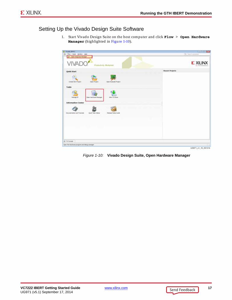
Setting Up the Vivado Design Suite Software1. Start Vivado Design Suite on the host computer and click Flow > Open Hardware
Manager (highlighted in Figure 1-10).X-Ref Target - Figure 1-10
Figure 1-10: Vivado Design Suite, Open Hardware Manager
Send Feedback
18 www.xilinx.com VC7222 IBERT Getting Started GuideUG971 (v5.1) September 17, 2014
Chapter 1: VC7222 IBERT Getting Started Guide
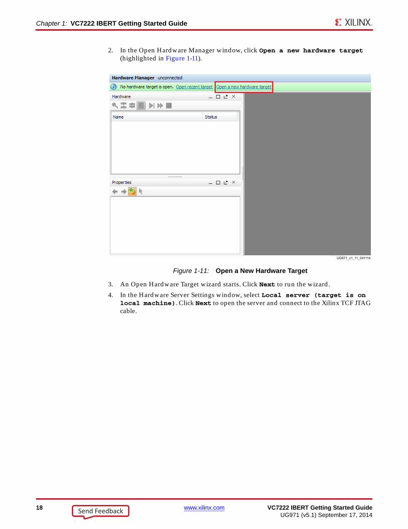
2. In the Open Hardware Manager window, click Open a new hardware target (highlighted in Figure 1-11).
3. An Open Hardware Target wizard starts. Click Next to run the wizard.
4. In the Hardware Server Settings window, select Local server (target is on local machine). Click Next to open the server and connect to the Xilinx TCF JTAG cable.
X-Ref Target - Figure 1-11
Figure 1-11: Open a New Hardware Target
Send Feedback

VC7222 IBERT Getting Started Guide www.xilinx.com 19UG971 (v5.1) September 17, 2014
Running the GTH IBERT Demonstration
5. In the Select Hardware Target window, the xilinx_tcf cable appears under Hardware Targets, and the JTAG chain contents of the selected cable appear under Hardware Devices (Figure 1-12). Select the xilinx_tcf target and keep the JTAG Clock Frequency at the default value (15 MHz). Click Next.
6. In the Open Hardware Target Summary window, click Finish. The wizard closes and the Vivado Design Suite opens the hardware target.
X-Ref Target - Figure 1-12
Figure 1-12: Select Hardware Target
Send Feedback
20 www.xilinx.com VC7222 IBERT Getting Started GuideUG971 (v5.1) September 17, 2014
Chapter 1: VC7222 IBERT Getting Started Guide
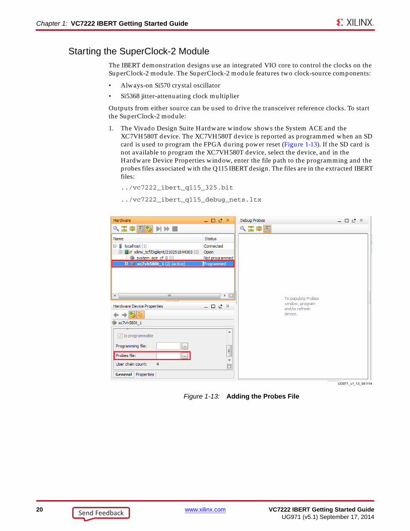
Starting the SuperClock-2 ModuleThe IBERT demonstration designs use an integrated VIO core to control the clocks on the SuperClock-2 module. The SuperClock-2 module features two clock-source components:
• Always-on Si570 crystal oscillator
• Si5368 jitter-attenuating clock multiplier
Outputs from either source can be used to drive the transceiver reference clocks. To start the SuperClock-2 module:
1. The Vivado Design Suite Hardware window shows the System ACE and the XC7VH580T device. The XC7VH580T device is reported as programmed when an SD card is used to program the FPGA during power reset (Figure 1-13). If the SD card is not available to program the XC7VH580T device, select the device, and in the Hardware Device Properties window, enter the file path to the programming and the probes files associated with the Q115 IBERT design. The files are in the extracted IBERT files:
../vc7222_ibert_q115_325.bit
../vc7222_ibert_q115_debug_nets.ltx
X-Ref Target - Figure 1-13
Figure 1-13: Adding the Probes File
Send Feedback
VC7222 IBERT Getting Started Guide www.xilinx.com 21UG971 (v5.1) September 17, 2014
Running the GTH IBERT Demonstration
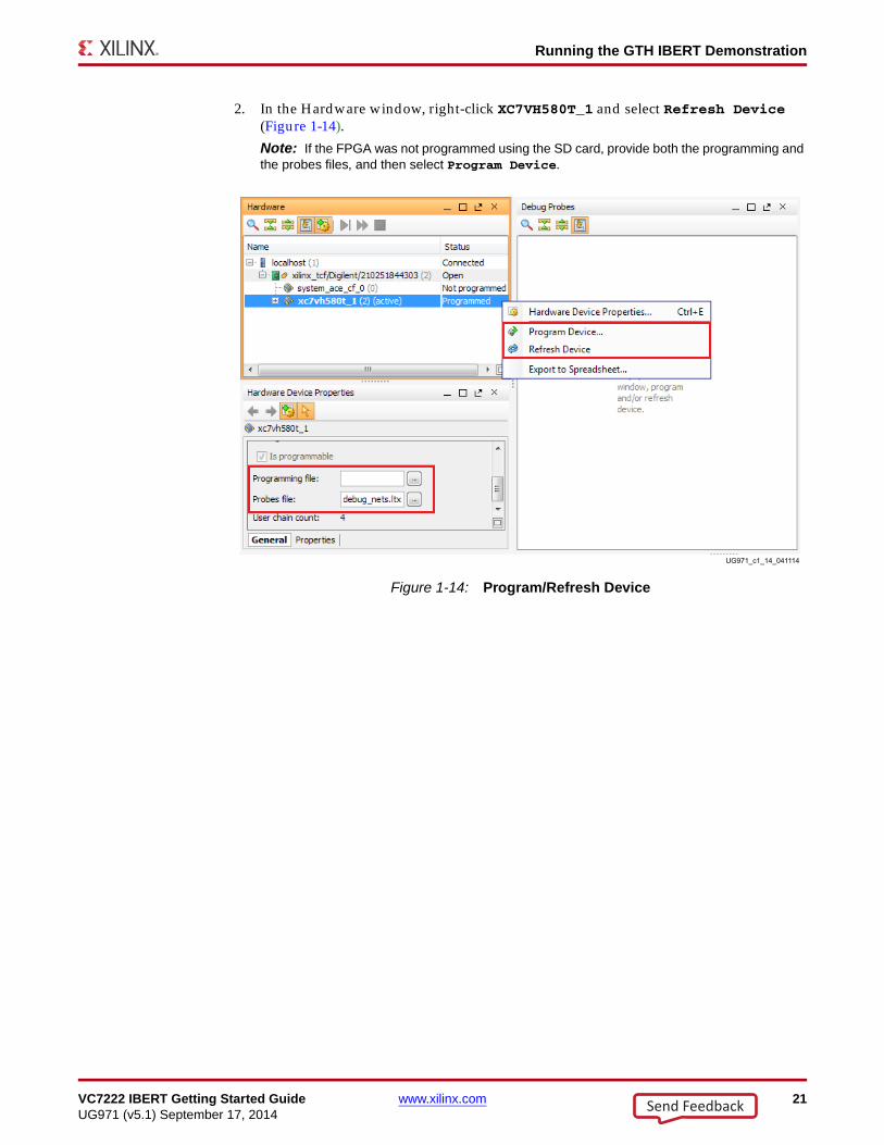
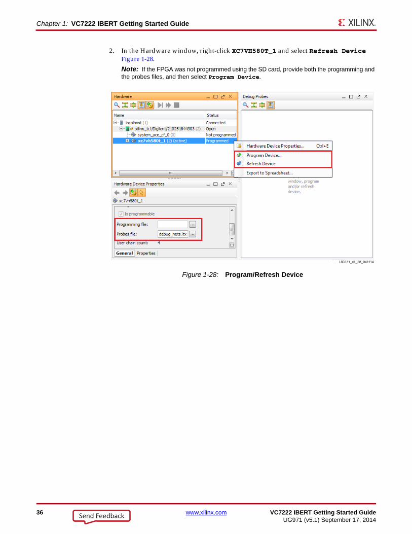
2. In the Hardware window, right-click XC7VH580T_1 and select Refresh Device (Figure 1-14).
Note: If the FPGA was not programmed using the SD card, provide both the programming and the probes files, and then select Program Device.
X-Ref Target - Figure 1-14
Figure 1-14: Program/Refresh Device
Send Feedback
22 www.xilinx.com VC7222 IBERT Getting Started GuideUG971 (v5.1) September 17, 2014
Chapter 1: VC7222 IBERT Getting Started Guide
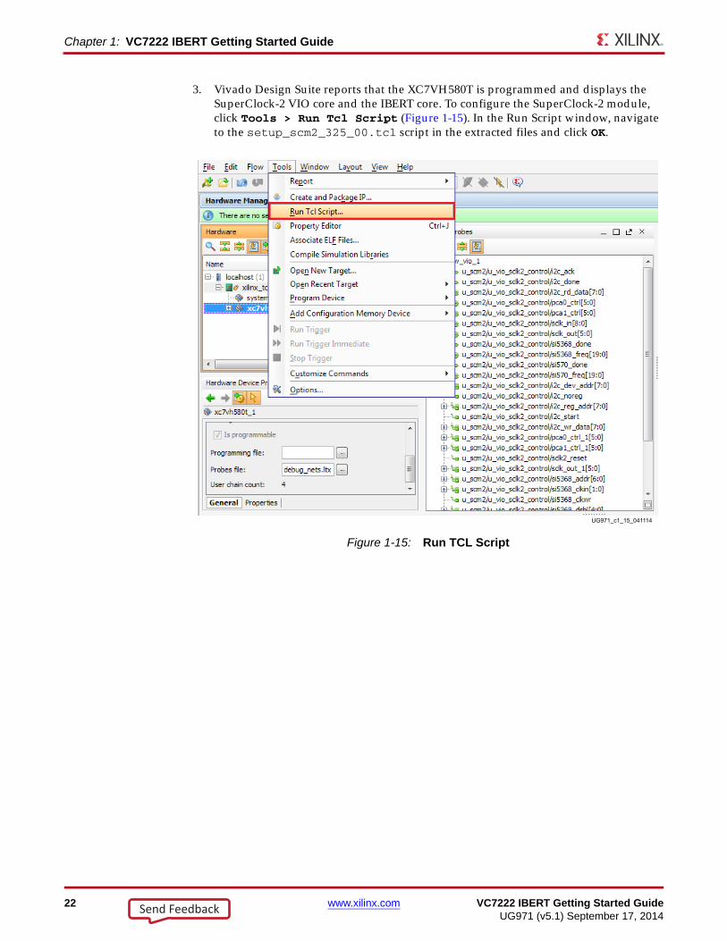
3. Vivado Design Suite reports that the XC7VH580T is programmed and displays the SuperClock-2 VIO core and the IBERT core. To configure the SuperClock-2 module, click Tools > Run Tcl Script (Figure 1-15). In the Run Script window, navigate to the setup_scm2_325_00.tcl script in the extracted files and click OK.
X-Ref Target - Figure 1-15
Figure 1-15: Run TCL Script
Send Feedback
VC7222 IBERT Getting Started Guide www.xilinx.com 23UG971 (v5.1) September 17, 2014
Running the GTH IBERT Demonstration
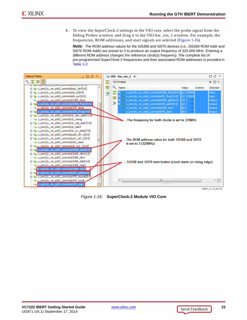
4. To view the SuperClock-2 settings in the VIO core, select the probe signal from the Debug Probes window and drag it to the VIO-hw_vio_1 window. For example, the frequencies, ROM addresses, and start signals are selected (Figure 1-16).
Note: The ROM address values for the Si5368 and Si570 devices (i.e., Si5368 ROM Addr and Si570 ROM Addr) are preset to 3 to produce an output frequency of 325.000 MHz. Entering a different ROM address changes the reference clock(s) frequency. The complete list of pre-programmed SuperClock-2 frequencies and their associated ROM addresses is provided in Table 1-2.
X-Ref Target - Figure 1-16
Figure 1-16: SuperClock-2 Module VIO Core
Send Feedback
24 www.xilinx.com VC7222 IBERT Getting Started GuideUG971 (v5.1) September 17, 2014
Chapter 1: VC7222 IBERT Getting Started Guide
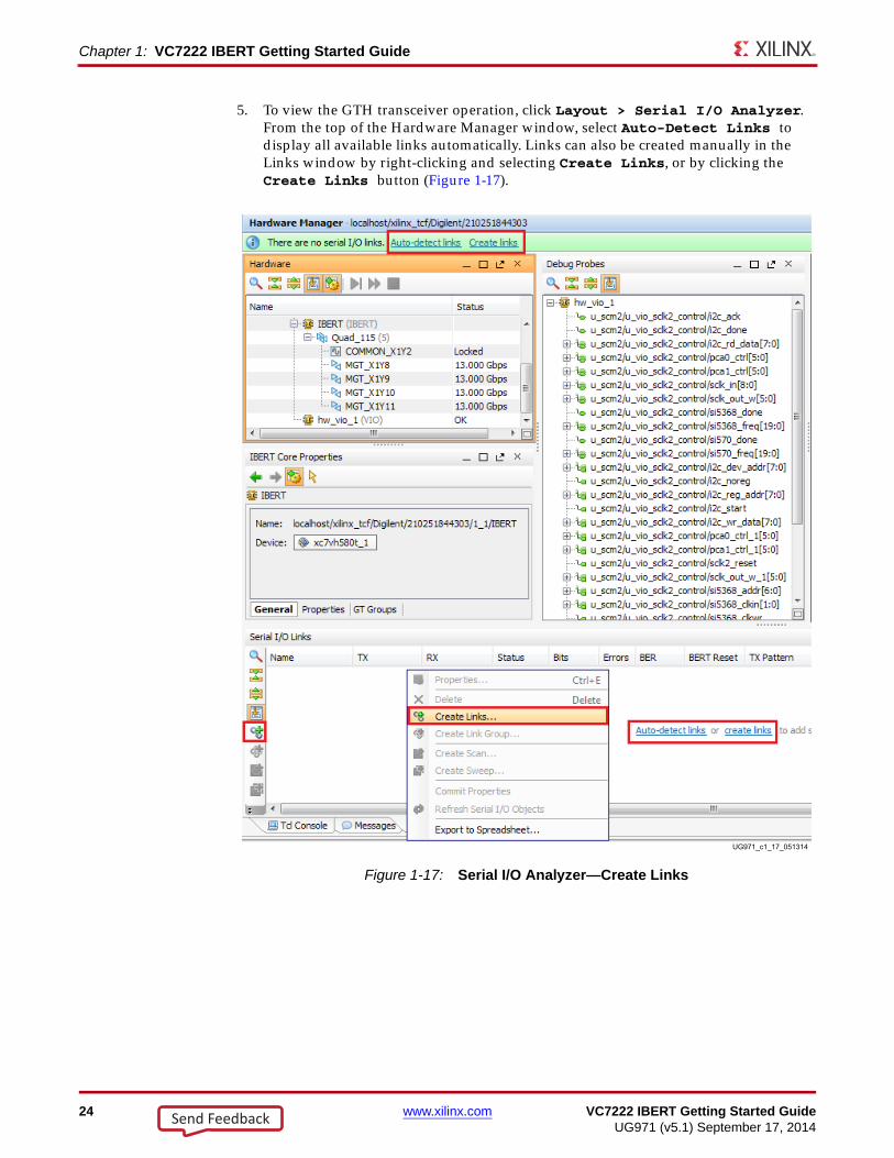
5. To view the GTH transceiver operation, click Layout > Serial I/O Analyzer. From the top of the Hardware Manager window, select Auto-Detect Links to display all available links automatically. Links can also be created manually in the Links window by right-clicking and selecting Create Links, or by clicking the Create Links button (Figure 1-17).
X-Ref Target - Figure 1-17
Figure 1-17: Serial I/O Analyzer—Create Links
Send Feedback
VC7222 IBERT Getting Started Guide www.xilinx.com 25UG971 (v5.1) September 17, 2014
Running the GTH IBERT Demonstration
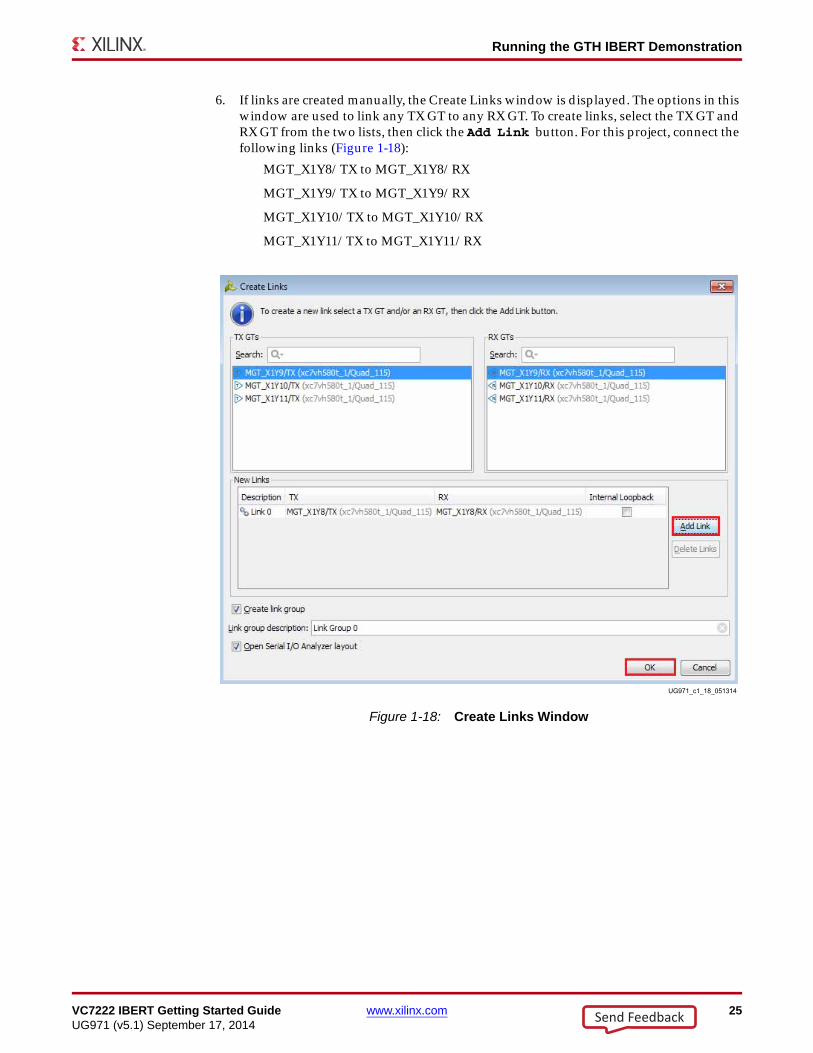
6. If links are created manually, the Create Links window is displayed. The options in this window are used to link any TX GT to any RX GT. To create links, select the TX GT and RX GT from the two lists, then click the Add Link button. For this project, connect the following links (Figure 1-18):
MGT_X1Y8/TX to MGT_X1Y8/RX
MGT_X1Y9/TX to MGT_X1Y9/RX
MGT_X1Y10/TX to MGT_X1Y10/RX
MGT_X1Y11/TX to MGT_X1Y11/RXX-Ref Target - Figure 1-18
Figure 1-18: Create Links Window
Send Feedback
26 www.xilinx.com VC7222 IBERT Getting Started GuideUG971 (v5.1) September 17, 2014
Chapter 1: VC7222 IBERT Getting Started Guide
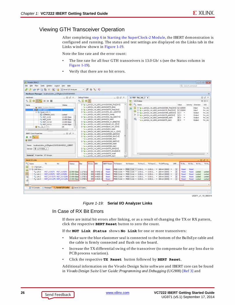
Viewing GTH Transceiver OperationAfter completing step 6 in Starting the SuperClock-2 Module, the IBERT demonstration is configured and running. The status and test settings are displayed on the Links tab in the Links window shown in Figure 1-19.
Note the line rate and the error count:
• The line rate for all four GTH transceivers is 13.0 Gb/s (see the Status column in Figure 1-19).
• Verify that there are no bit errors.
In Case of RX Bit Errors
If there are initial bit errors after linking, or as a result of changing the TX or RX pattern, click the respective BERT Reset button to zero the count.
If the MGT Link Status shows No Link for one or more transceivers:
• Make sure the blue elastomer seal is connected to the bottom of the BullsEye cable and the cable is firmly connected and flush on the board.
• Increase the TX differential swing of the transceiver (to compensate for any loss due to PCB process variation).
• Click the respective TX Reset button followed by BERT Reset.
Additional information on the Vivado Design Suite software and IBERT core can be found in Vivado Design Suite User Guide: Programming and Debugging (UG908) [Ref 3] and
X-Ref Target - Figure 1-19
Figure 1-19: Serial I/O Analyzer Links
Send Feedback
VC7222 IBERT Getting Started Guide www.xilinx.com 27UG971 (v5.1) September 17, 2014
Running the GTZ IBERT Demonstration
LogiCORE IP Integrated Bit Error Ratio Tester (IBERT) for 7 Series GTH Transceivers Product Guide for Vivado Design Suite (PG152) [Ref 4].
Closing the IBERT DemonstrationTo stop the IBERT demonstration:
1. Close the Vivado Design Suite application by selecting File > Exit.
2. Place the main power switch SW1 in the off position.
Running the GTZ IBERT DemonstrationThe GTZ IBERT demonstration example provided here operates all 8 lanes of the GTZ transceiver at the same time.
Note: The VC7222 board ships with one BullsEye cable while the provided example uses two cables and activates all 8 GTZ lanes. In the absence of a second BullsEye cable, only one of the GTZ quads, Q300A or Q300B (4 lanes), can be observed at a time.
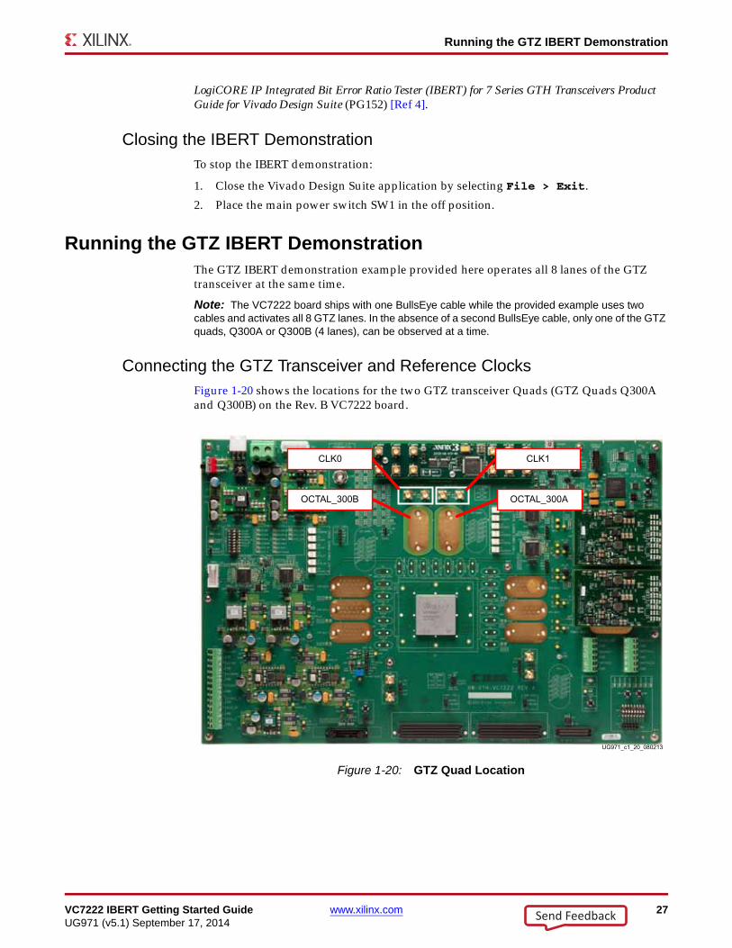
Connecting the GTZ Transceiver and Reference ClocksFigure 1-20 shows the locations for the two GTZ transceiver Quads (GTZ Quads Q300A and Q300B) on the Rev. B VC7222 board. X-Ref Target - Figure 1-20
Figure 1-20: GTZ Quad Location
Send Feedback
28 www.xilinx.com VC7222 IBERT Getting Started GuideUG971 (v5.1) September 17, 2014
Chapter 1: VC7222 IBERT Getting Started Guide
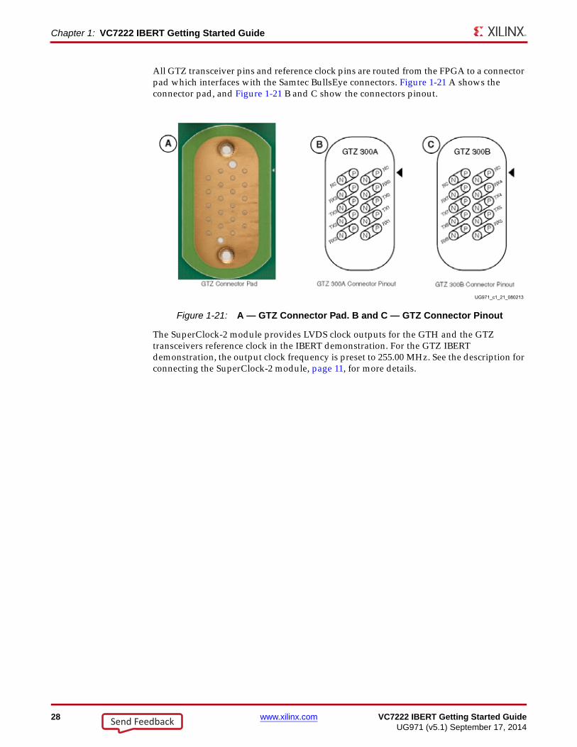
All GTZ transceiver pins and reference clock pins are routed from the FPGA to a connector pad which interfaces with the Samtec BullsEye connectors. Figure 1-21 A shows the connector pad, and Figure 1-21 B and C show the connectors pinout.
The SuperClock-2 module provides LVDS clock outputs for the GTH and the GTZ transceivers reference clock in the IBERT demonstration. For the GTZ IBERT demonstration, the output clock frequency is preset to 255.00 MHz. See the description for connecting the SuperClock-2 module, page 11, for more details.
X-Ref Target - Figure 1-21
Figure 1-21: A — GTZ Connector Pad. B and C — GTZ Connector Pinout
Send Feedback

VC7222 IBERT Getting Started Guide www.xilinx.com 29UG971 (v5.1) September 17, 2014
Running the GTZ IBERT Demonstration
Attach the GTZ Quad Connector
Before connecting the BullsEye cable assembly to the board, firmly secure the blue elastomer seal provided with the cable assembly to the bottom of the connector housing if it is not already inserted (see Figure 1-4).
Attach the Samtec BullsEye connector to either GTZ Quad Q300A or Q300B (Figure 1-22), aligning the two indexing pins on the bottom of the connector with the guide holes on the board. Hold the connector flush with the board and fasten it by tightening the two captive screws.
Caution! Figure 1-22 shows BullsEye cables connected to both Q300A and Q300B. If only one BullsEye cable is available, make sure to power down the board before moving the BullsEye cable to the second half of the GTZ lanes.
X-Ref Target - Figure 1-22
Figure 1-22: BullsEye Connector Attached to GTZ Quads Q300A and Q300B
Send Feedback
30 www.xilinx.com VC7222 IBERT Getting Started GuideUG971 (v5.1) September 17, 2014
Chapter 1: VC7222 IBERT Getting Started Guide
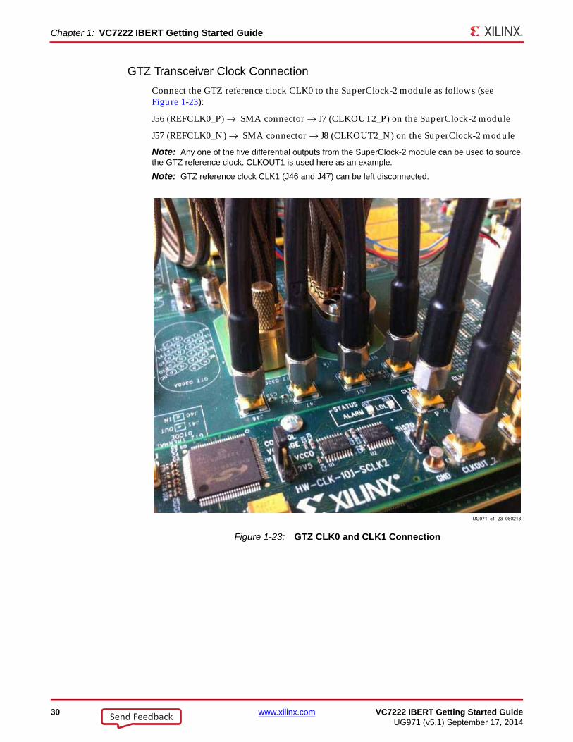
GTZ Transceiver Clock Connection
Connect the GTZ reference clock CLK0 to the SuperClock-2 module as follows (see Figure 1-23):
J56 (REFCLK0_P) → SMA connector → J7 (CLKOUT2_P) on the SuperClock-2 module
J57 (REFCLK0_N) → SMA connector → J8 (CLKOUT2_N) on the SuperClock-2 module
Note: Any one of the five differential outputs from the SuperClock-2 module can be used to source the GTZ reference clock. CLKOUT1 is used here as an example.
Note: GTZ reference clock CLK1 (J46 and J47) can be left disconnected.X-Ref Target - Figure 1-23
Figure 1-23: GTZ CLK0 and CLK1 Connection
Send Feedback
VC7222 IBERT Getting Started Guide www.xilinx.com 31UG971 (v5.1) September 17, 2014
Running the GTZ IBERT Demonstration
GTZ TX/RX Loopback Connections
See Figure 1-21 to identify the location of the P and N pins of the GTZ transmitters and receivers lanes. Use eight SMA female-to-female (F-F) adapters (Figure 1-6) to connect the transmit and receive cables as shown in Figure 1-7 and detailed in the following list:
• TX0_P → SMA F-F Adapter → RX0_P
• TX0_N → SMA F-F Adapter → RX0_N
• TX1_P → SMA F-F Adapter → RX1_P
• TX1_N → SMA F-F Adapter → RX1_N
• TX2_P → SMA F-F Adapter → RX2_P
• TX2_N → SMA F-F Adapter → RX2_N
• TX3_P → SMA F-F Adapter → RX3_P
• TX3_N → SMA F-F Adapter → RX3_N
• TX4_P → SMA F-F Adapter → RX4_P
• TX4_N → SMA F-F Adapter → RX4_N
• TX5_P → SMA F-F Adapter → RX5_P
• TX5_N → SMA F-F Adapter → RX5_N
• TX6_P → SMA F-F Adapter → RX6_P
• TX6_N → SMA F-F Adapter → RX6_N
• TX7_P → SMA F-F Adapter → RX7_P
• TX7_N → SMA F-F Adapter → RX7_N
Note: To ensure good connectivity, it is recommended that the adapters be secured with a wrench, however do not over-tighten the SMA connectors.
Send Feedback
32 www.xilinx.com VC7222 IBERT Getting Started GuideUG971 (v5.1) September 17, 2014
Chapter 1: VC7222 IBERT Getting Started Guide
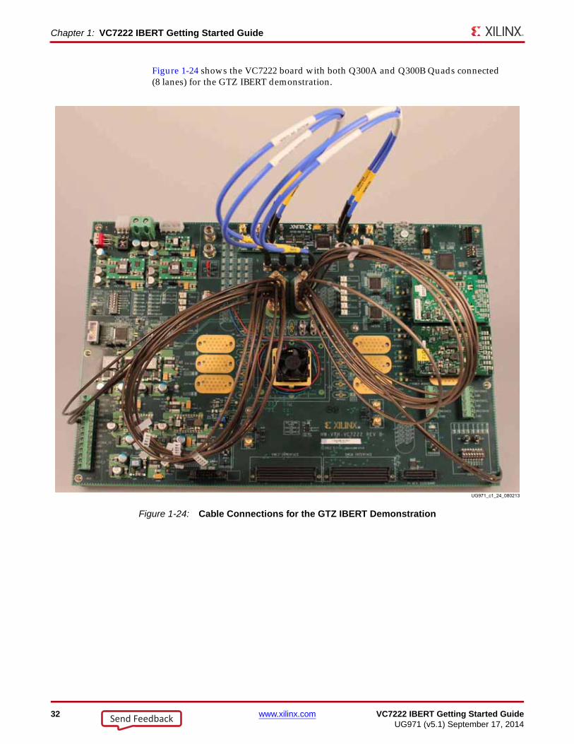
Figure 1-24 shows the VC7222 board with both Q300A and Q300B Quads connected (8 lanes) for the GTZ IBERT demonstration.
X-Ref Target - Figure 1-24
Figure 1-24: Cable Connections for the GTZ IBERT Demonstration
Send Feedback
VC7222 IBERT Getting Started Guide www.xilinx.com 33UG971 (v5.1) September 17, 2014
Running the GTZ IBERT Demonstration
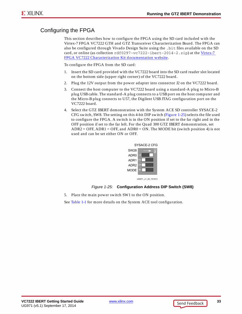
Configuring the FPGAThis section describes how to configure the FPGA using the SD card included with the Virtex-7 FPGA VC7222 GTH and GTZ Transceiver Characterization Board. The FPGA can also be configured through Vivado Design Suite using the .bit files available on the SD card, or online (as collection rdf0297-vc7222-ibert-2014-2.zip) at the Virtex-7 FPGA VC7222 Characterization Kit documentation website.
To configure the FPGA from the SD card:
1. Insert the SD card provided with the VC7222 board into the SD card reader slot located on the bottom side (upper right corner) of the VC7222 board.
2. Plug the 12V output from the power adapter into connector J2 on the VC7222 board.
3. Connect the host computer to the VC7222 board using a standard-A plug to Micro-B plug USB cable. The standard-A plug connects to a USB port on the host computer and the Micro-B plug connects to U57, the Digilent USB JTAG configuration port on the VC7222 board.
4. Select the GTZ IBERT demonstration with the System ACE SD controller SYSACE-2 CFG switch, SW8. The setting on this 4-bit DIP switch (Figure 1-25) selects the file used to configure the FPGA. A switch is in the ON position if set to the far right and in the OFF position if set to the far left. For the Quad 300 GTZ IBERT demonstration, set ADR2 = OFF, ADR1 = OFF, and ADR0 = ON. The MODE bit (switch position 4) is not used and can be set either ON or OFF.
5. Place the main power switch SW1 to the ON position.
See Table 1-1 for more details on the System ACE tool configuration.
X-Ref Target - Figure 1-25
Figure 1-25: Configuration Address DIP Switch (SW8)
Send Feedback

34 www.xilinx.com VC7222 IBERT Getting Started GuideUG971 (v5.1) September 17, 2014
Chapter 1: VC7222 IBERT Getting Started Guide
Setting up the Vivado Design Suite SoftwareThe procedure to launch the Vivado Suite is detailed in Setting Up the Vivado Design Suite Software, page 17.
In the Open Hardware Target window it is highly recommended to lower the JTAG clock frequency to 10 MHz or lower for reliable JTAG communication during the GTZ demonstration (Figure 1-26).
Starting the SuperClock-2 ModuleThe IBERT demonstration designs use an integrated VIO core to control the clocks on the SuperClock-2 module. The SuperClock-2 module features two clock-source components:
• An always-on Si570 crystal oscillator
• An Si5368 jitter-attenuating clock multiplier
Outputs from either source can be used to drive the transceiver reference clocks.
X-Ref Target - Figure 1-26
Figure 1-26: Select Hardware Target
Send Feedback
VC7222 IBERT Getting Started Guide www.xilinx.com 35UG971 (v5.1) September 17, 2014
Running the GTZ IBERT Demonstration
To start the SuperClock-2 module:
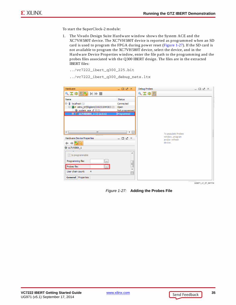
1. The Vivado Design Suite Hardware window shows the System ACE and the XC7VH580T device. The XC7VH580T device is reported as programmed when an SD card is used to program the FPGA during power reset (Figure 1-27). If the SD card is not available to program the XC7VH580T device, select the device, and in the Hardware Device Properties window, enter the file path to the programming and the probes files associated with the Q300 IBERT design. The files are in the extracted IBERT files:
../vc7222_ibert_q300_225.bit
../vc7222_ibert_q300_debug_nets.ltx
X-Ref Target - Figure 1-27
Figure 1-27: Adding the Probes File
Send Feedback
36 www.xilinx.com VC7222 IBERT Getting Started GuideUG971 (v5.1) September 17, 2014
Chapter 1: VC7222 IBERT Getting Started Guide
2. In the Hardware window, right-click XC7VH580T_1 and select Refresh Device Figure 1-28.
Note: If the FPGA was not programmed using the SD card, provide both the programming and the probes files, and then select Program Device.
X-Ref Target - Figure 1-28
Figure 1-28: Program/Refresh Device
Send Feedback

VC7222 IBERT Getting Started Guide www.xilinx.com 37UG971 (v5.1) September 17, 2014
Running the GTZ IBERT Demonstration
3. Vivado Design Suite reports that the XC7VH580T is programmed and displays the SuperClock-2 VIO core and the IBERT core. To configure the SuperClock-2 module, click Tools > Run Tcl Script (Figure 1-29). In the Run Script window, navigate to the setup_scm2_255_00.tcl script in the extracted files and click OK.
X-Ref Target - Figure 1-29
Figure 1-29: Run TCL Script
Send Feedback

38 www.xilinx.com VC7222 IBERT Getting Started GuideUG971 (v5.1) September 17, 2014
Chapter 1: VC7222 IBERT Getting Started Guide
4. To view the SuperClock-2 settings in the VIO core, select the probe signal from the Debug Probes window and drag it to the VIO-hw_vio_1 window. For example, the frequencies, ROM addresses, and start signals are selected (Figure 1-30).
Note: The ROM address values for the Si5368 and Si570 devices (i.e., Si5368 ROM Addr and Si570 ROM Addr) are preset to 81 to produce an output frequency of 255.000 MHz. Entering a different ROM address changes the reference clock(s) frequency. The complete list of pre-programmed SuperClock-2 frequencies and their associated ROM addresses is provided in Table 1-2.
X-Ref Target - Figure 1-30
Figure 1-30: SuperClock-2 Module VIO Core
Send Feedback
VC7222 IBERT Getting Started Guide www.xilinx.com 39UG971 (v5.1) September 17, 2014
Running the GTZ IBERT Demonstration
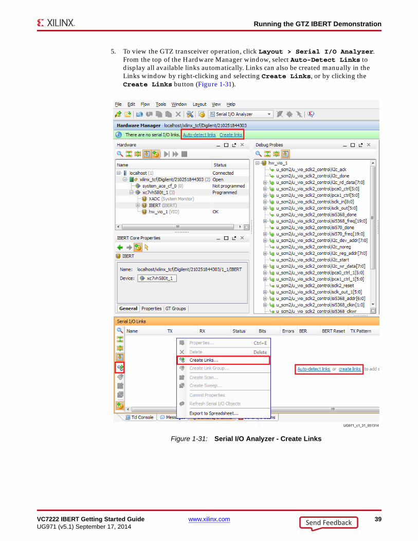
5. To view the GTZ transceiver operation, click Layout > Serial I/O Analyzer. From the top of the Hardware Manager window, select Auto-Detect Links to display all available links automatically. Links can also be created manually in the Links window by right-clicking and selecting Create Links, or by clicking the Create Links button (Figure 1-31).
X-Ref Target - Figure 1-31
Figure 1-31: Serial I/O Analyzer - Create Links
Send Feedback
40 www.xilinx.com VC7222 IBERT Getting Started GuideUG971 (v5.1) September 17, 2014
Chapter 1: VC7222 IBERT Getting Started Guide
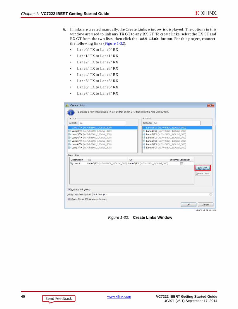
6. If links are created manually, the Create Links window is displayed. The options in this window are used to link any TX GT to any RX GT. To create links, select the TX GT and RX GT from the two lists, then click the Add Link button. For this project, connect the following links (Figure 1-32):
• Lane0/TX to Lane0/RX
• Lane1/TX to Lane1/RX
• Lane2/TX to Lane2/RX
• Lane3/TX to Lane3/RX
• Lane4/TX to Lane4/RX
• Lane5/TX to Lane5/RX
• Lane6/TX to Lane6/RX
• Lane7/TX to Lane7/RXX-Ref Target - Figure 1-32
Figure 1-32: Create Links Window
Send Feedback
VC7222 IBERT Getting Started Guide www.xilinx.com 41UG971 (v5.1) September 17, 2014
Running the GTZ IBERT Demonstration
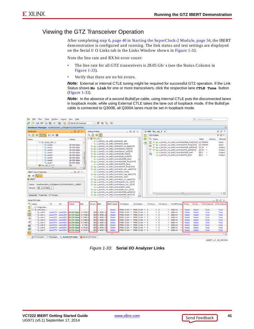
Viewing the GTZ Transceiver OperationAfter completing step 6, page 40 in Starting the SuperClock-2 Module, page 34, the IBERT demonstration is configured and running. The link status and test settings are displayed on the Serial I/O Links tab in the Links Window shown in Figure 1-33.
Note the line rate and RX bit error count:
• The line rate for all GTZ transceivers is 28.05 Gb/s (see the Status Column in Figure 1-33).
• Verify that there are no bit errors.
Note: External or internal CTLE tuning might be required for successful GTZ operation. If the Link Status shows No Link for one or more transceivers, click the respective lane CTLE Tune button (Figure 1-33).
Note: In the absence of a second BullsEye cable, using Internal CTLE puts the disconnected lanes in loopback mode, while using External CTLE takes the lane out of loopback mode. If the BullsEye cable is connected to Q300B, all Q300A lanes must be set in loopback mode.
X-Ref Target - Figure 1-33
Figure 1-33: Serial I/O Analyzer Links
Send Feedback
42 www.xilinx.com VC7222 IBERT Getting Started GuideUG971 (v5.1) September 17, 2014
Chapter 1: VC7222 IBERT Getting Started Guide
In Case of RX Bit Errors
If there are initial bit errors after linking, or as a result of changing the TX or RX pattern, click the respective BERT Reset button to zero the count.
Additional information on the Vivado Design Suite and IBERT core can be found in Vivado Design Suite User Guide: Programming and Debugging (UG908) [Ref 3] and in LogiCORE IP Integrated Bit Error Ratio Tester (IBERT) for 7 Series GTX Transceivers Product Guide for Vivado Design Suite (PG132) [Ref 4].
Closing the IBERT DemonstrationTo stop the IBERT demonstration:
1. Close the Vivado Design Suite by selecting File > Exit.
2. Place the main power switch SW1 in the OFF position.
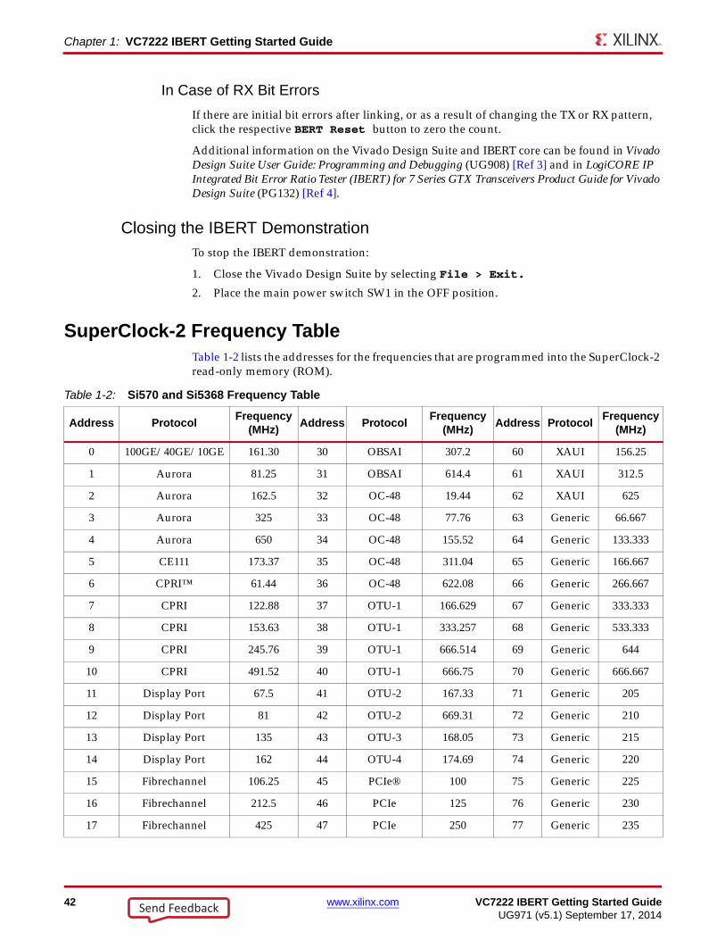
SuperClock-2 Frequency TableTable 1-2 lists the addresses for the frequencies that are programmed into the SuperClock-2 read-only memory (ROM).
Table 1-2: Si570 and Si5368 Frequency Table
Address ProtocolFrequency
(MHz)Address Protocol
Frequency (MHz)
Address ProtocolFrequency
(MHz)
0 100GE/40GE/10GE 161.30 30 OBSAI 307.2 60 XAUI 156.25
1 Aurora 81.25 31 OBSAI 614.4 61 XAUI 312.5
2 Aurora 162.5 32 OC-48 19.44 62 XAUI 625
3 Aurora 325 33 OC-48 77.76 63 Generic 66.667
4 Aurora 650 34 OC-48 155.52 64 Generic 133.333
5 CE111 173.37 35 OC-48 311.04 65 Generic 166.667
6 CPRI™ 61.44 36 OC-48 622.08 66 Generic 266.667
7 CPRI 122.88 37 OTU-1 166.629 67 Generic 333.333
8 CPRI 153.63 38 OTU-1 333.257 68 Generic 533.333
9 CPRI 245.76 39 OTU-1 666.514 69 Generic 644
10 CPRI 491.52 40 OTU-1 666.75 70 Generic 666.667
11 Display Port 67.5 41 OTU-2 167.33 71 Generic 205
12 Display Port 81 42 OTU-2 669.31 72 Generic 210
13 Display Port 135 43 OTU-3 168.05 73 Generic 215
14 Display Port 162 44 OTU-4 174.69 74 Generic 220
15 Fibrechannel 106.25 45 PCIe® 100 75 Generic 225
16 Fibrechannel 212.5 46 PCIe 125 76 Generic 230
17 Fibrechannel 425 47 PCIe 250 77 Generic 235
Send Feedback

VC7222 IBERT Getting Started Guide www.xilinx.com 43UG971 (v5.1) September 17, 2014
SuperClock-2 Frequency Table
18 GigE 62.5 48 SATA 75 78 Generic 240
19 GigE 125 49 SATA 150 79 Generic 245
20 GigE 250 50 SATA 300 80 Generic 250
21 GigE 500 51 SATA 600 81 Generic 255
22 GPON 187.5 52 SDI 74.25 82 Generic 260
23 Interlaken 132.813 53 SDI 148.5 83 Generic 265
24 Interlaken 195.313 54 SDI 297 84 Generic 270
25 Interlaken 265.625 55 SDI 594 85 Generic 275
26 Interlaken 390.625 56 SMPTE435M 167.063 86 Generic 280
27 Interlaken 531.25 57 SMPTE435M 334.125 87 Generic 285
28 OBSAI 76.8 58 SMPTE435M 668.25 88 Generic 290
29 OBSAI 153.6 59 XAUI 78.125 89 Generic 295
90 Generic 300 103 Generic 365 116 Generic 430
91 Generic 305 104 Generic 370 117 Generic 435
92 Generic 310 105 Generic 375 118 Generic 440
93 Generic 315 106 Generic 380 119 Generic 445
94 Generic 320 107 Generic 385 120 Generic 450
95 Generic 325 108 Generic 390 121 Generic 455
96 Generic 330 109 Generic 395 122 Generic 460
97 Generic 335 110 Generic 400 123 Generic 465
98 Generic 340 111 Generic 405 124 Generic 470
99 Generic 345 112 Generic 410 125 Generic 475
100 Generic 350 113 Generic 415 126 Generic 480
101 Generic 355 114 Generic 420 127 Generic 485
102 Generic 360 115 Generic 425
Table 1-2: Si570 and Si5368 Frequency Table (Cont’d)
Address ProtocolFrequency
(MHz)Address Protocol
Frequency (MHz)
Address ProtocolFrequency
(MHz)
Send Feedback

44 www.xilinx.com VC7222 IBERT Getting Started GuideUG971 (v5.1) September 17, 2014
Chapter 1: VC7222 IBERT Getting Started Guide
Send Feedback
VC7222 IBERT Getting Started Guide www.xilinx.com 45UG971 (v5.1) September 17, 2014
Chapter 2
Creating the GTH IBERT Core
Note: Vivado® Design Suite 2014.2 is required to rebuild the designs shown here.
This section provides a procedure to create a single Quad GTH IBERT core with integrated SuperClock-2 controller. The procedure assumes Quad 115 and 13.0 Gb/s line rate, but cores for any of the GTH Quads with any supported line rate can be created following the same series of steps.
For more details on generating IBERT cores, see the Vivado Design Suite User Guide: Programming and Debugging (UG908) [Ref 3].
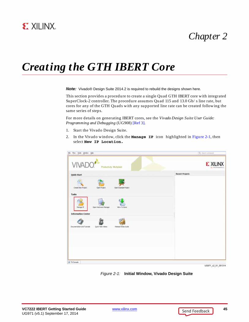
1. Start the Vivado Design Suite.
2. In the Vivado window, click the Manage IP icon highlighted in Figure 2-1, then select New IP Location.
X-Ref Target - Figure 2-1
Figure 2-1: Initial Window, Vivado Design Suite
Send Feedback
46 www.xilinx.com VC7222 IBERT Getting Started GuideUG971 (v5.1) September 17, 2014
Chapter 2: Creating the GTH IBERT Core
3. When the Create a New Customized IP Location dialog window opens (not shown), click Next.
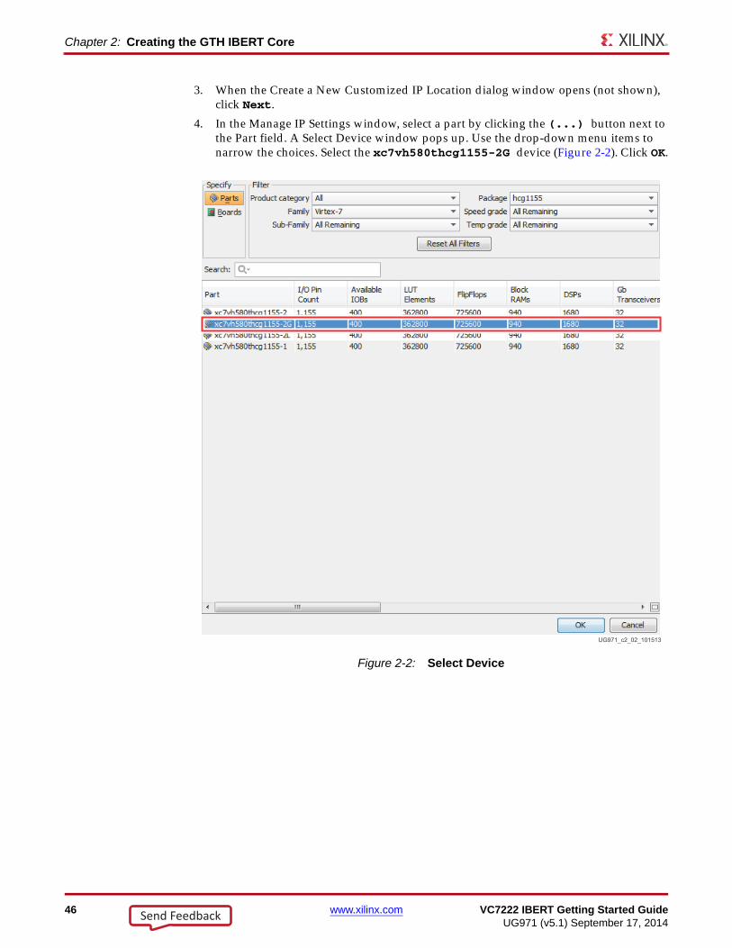
4. In the Manage IP Settings window, select a part by clicking the (...) button next to the Part field. A Select Device window pops up. Use the drop-down menu items to narrow the choices. Select the xc7vh580thcg1155-2G device (Figure 2-2). Click OK.
X-Ref Target - Figure 2-2
Figure 2-2: Select Device
Send Feedback
VC7222 IBERT Getting Started Guide www.xilinx.com 47UG971 (v5.1) September 17, 2014
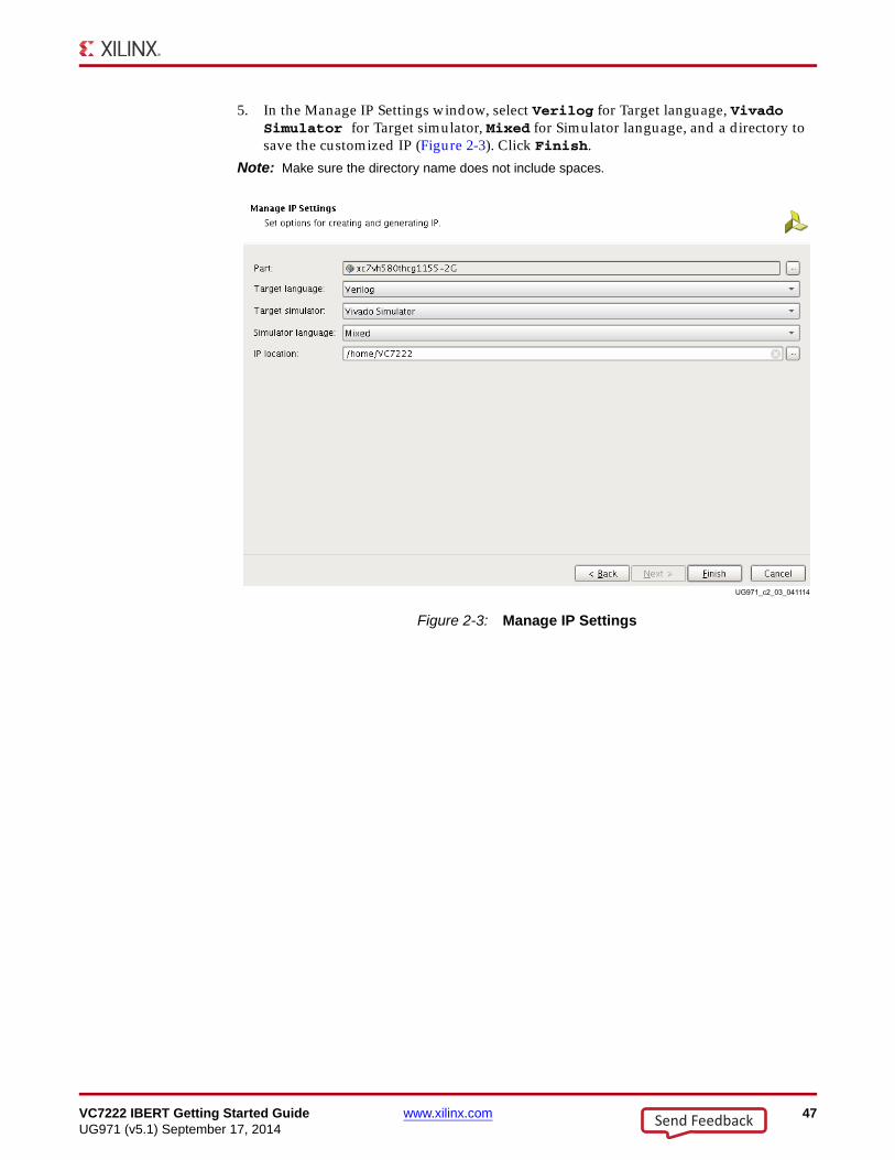
5. In the Manage IP Settings window, select Verilog for Target language, Vivado Simulator for Target simulator, Mixed for Simulator language, and a directory to save the customized IP (Figure 2-3). Click Finish.
Note: Make sure the directory name does not include spaces.X-Ref Target - Figure 2-3
Figure 2-3: Manage IP Settings
Send Feedback
48 www.xilinx.com VC7222 IBERT Getting Started GuideUG971 (v5.1) September 17, 2014
Chapter 2: Creating the GTH IBERT Core
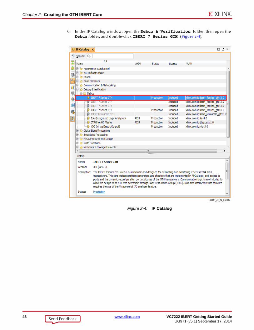
6. In the IP Catalog window, open the Debug & Verification folder, then open the Debug folder, and double-click IBERT 7 Series GTH (Figure 2-4).
X-Ref Target - Figure 2-4
Figure 2-4: IP Catalog
Send Feedback
VC7222 IBERT Getting Started Guide www.xilinx.com 49UG971 (v5.1) September 17, 2014
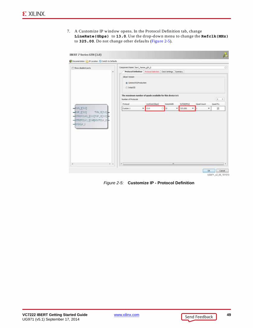
7. A Customize IP window opens. In the Protocol Definition tab, change LineRate(Gbps) to 13.0. Use the drop-down menu to change the Refclk(MHz) to 325.00. Do not change other defaults (Figure 2-5).
X-Ref Target - Figure 2-5
Figure 2-5: Customize IP - Protocol Definition
Send Feedback

50 www.xilinx.com VC7222 IBERT Getting Started GuideUG971 (v5.1) September 17, 2014
Chapter 2: Creating the GTH IBERT Core
8. In the Protocol Selection tab, use the Protocol Selected drop-down menu next to QUAD_115 to select Custom 1/13.0 Gbps (Figure 2-6).
X-Ref Target - Figure 2-6
Figure 2-6: Customize IP - Protocol Selection
Send Feedback

VC7222 IBERT Getting Started Guide www.xilinx.com 51UG971 (v5.1) September 17, 2014
9. In the Clock Settings tab, select DIFF SSTL15 for the I/O Standard, enter AL24 for P Package Pin and AL25 for N Package Pin (the FPGA pins that the system clock connects to), and ensure the Frequency is set to 200.00 (Figure 2-7). Click OK. Click Generate in the next window to generate the output products.
X-Ref Target - Figure 2-7
Figure 2-7: Customize IP - Clock Settings
Send Feedback
52 www.xilinx.com VC7222 IBERT Getting Started GuideUG971 (v5.1) September 17, 2014
Chapter 2: Creating the GTH IBERT Core
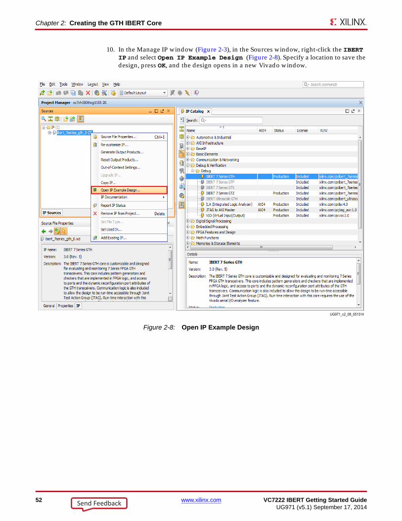
10. In the Manage IP window (Figure 2-3), in the Sources window, right-click the IBERT IP and select Open IP Example Design (Figure 2-8). Specify a location to save the design, press OK, and the design opens in a new Vivado window.
X-Ref Target - Figure 2-8
Figure 2-8: Open IP Example Design
Send Feedback

VC7222 IBERT Getting Started Guide www.xilinx.com 53UG971 (v5.1) September 17, 2014
11. In the new window, select Tools Run Tcl Script. In the Run Script window, navigate to add_scm2.tcl in the extracted files and press OK. The SuperClock-2 Module Design Sources and Constraints are automatically added to the example design (Figure 2-9).
X-Ref Target - Figure 2-9
Figure 2-9: Sources after Running add_scm2.tcl
Send Feedback
54 www.xilinx.com VC7222 IBERT Getting Started GuideUG971 (v5.1) September 17, 2014
Chapter 2: Creating the GTH IBERT Core
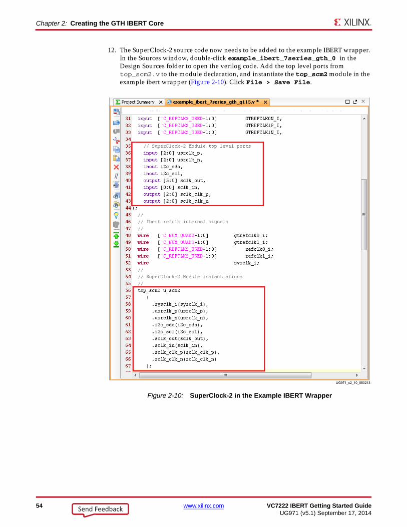
12. The SuperClock-2 source code now needs to be added to the example IBERT wrapper. In the Sources window, double-click example_ibert_7series_gth_0 in the Design Sources folder to open the verilog code. Add the top level ports from top_scm2.v to the module declaration, and instantiate the top_scm2 module in the example ibert wrapper (Figure 2-10). Click File > Save File.
X-Ref Target - Figure 2-10
Figure 2-10: SuperClock-2 in the Example IBERT Wrapper
Send Feedback

VC7222 IBERT Getting Started Guide www.xilinx.com 55UG971 (v5.1) September 17, 2014
13. In the Sources window, Design Sources should now reflect that the SuperClock-2 module is part of the example IBERT design (Figure 2-11).
X-Ref Target - Figure 2-11
Figure 2-11: Design Sources File Hierarchy
Send Feedback
56 www.xilinx.com VC7222 IBERT Getting Started GuideUG971 (v5.1) September 17, 2014
Chapter 2: Creating the GTH IBERT Core
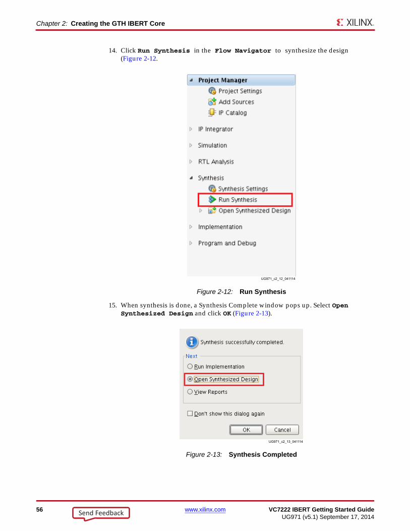
14. Click Run Synthesis in the Flow Navigator to synthesize the design (Figure 2-12.
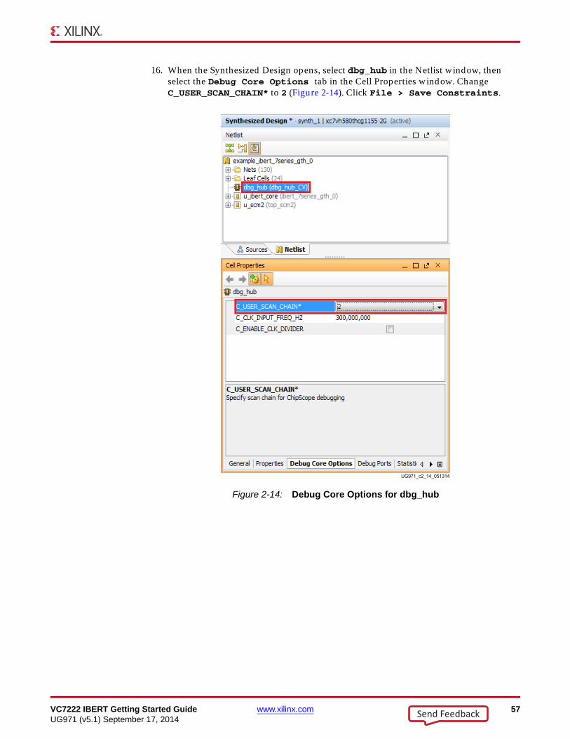
15. When synthesis is done, a Synthesis Complete window pops up. Select Open Synthesized Design and click OK (Figure 2-13).
X-Ref Target - Figure 2-12
Figure 2-12: Run Synthesis
X-Ref Target - Figure 2-13
Figure 2-13: Synthesis Completed
Send Feedback
VC7222 IBERT Getting Started Guide www.xilinx.com 57UG971 (v5.1) September 17, 2014
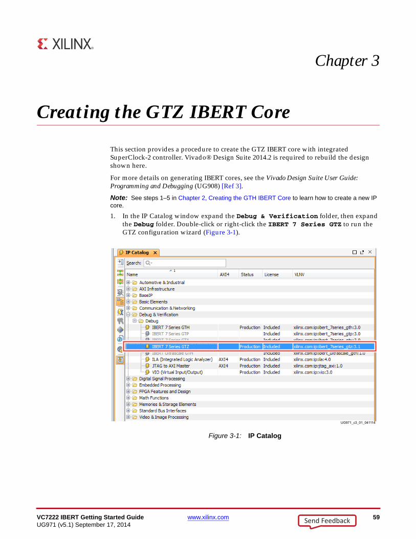
16. When the Synthesized Design opens, select dbg_hub in the Netlist window, then select the Debug Core Options tab in the Cell Properties window. Change C_USER_SCAN_CHAIN* to 2 (Figure 2-14). Click File > Save Constraints.
X-Ref Target - Figure 2-14
Figure 2-14: Debug Core Options for dbg_hub
Send Feedback

58 www.xilinx.com VC7222 IBERT Getting Started GuideUG971 (v5.1) September 17, 2014
Chapter 2: Creating the GTH IBERT Core
17. In the Program Manager, under Program and Debug, click Generate Bitstream (Figure 2-15). A window pops up asking if it is ok to launch implementation. Click Yes.
18. When the Bitstream Generation Completed dialog window appears, click Cancel (Figure 2-16).
19. Navigate to the ..\ibert_7series_gtz_0\ibert_7series_gtz_0_example\ibert_7series_gtz_0_example.runs\impl_1 directory to locate the generated bitstream.
X-Ref Target - Figure 2-15
Figure 2-15: Generate Bitstream
X-Ref Target - Figure 2-16
Figure 2-16: Bitstream Generation Completed
Send Feedback
VC7222 IBERT Getting Started Guide www.xilinx.com 59UG971 (v5.1) September 17, 2014
Chapter 3
Creating the GTZ IBERT Core
This section provides a procedure to create the GTZ IBERT core with integrated SuperClock-2 controller. Vivado® Design Suite 2014.2 is required to rebuild the design shown here.
For more details on generating IBERT cores, see the Vivado Design Suite User Guide: Programming and Debugging (UG908) [Ref 3].
Note: See steps 1–5 in Chapter 2, Creating the GTH IBERT Core to learn how to create a new IP core.
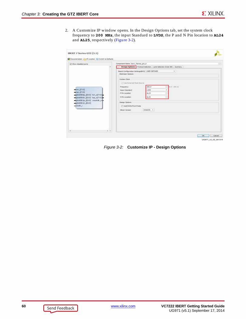
1. In the IP Catalog window expand the Debug & Verification folder, then expand the Debug folder. Double-click or right-click the IBERT 7 Series GTZ to run the GTZ configuration wizard (Figure 3-1).
X-Ref Target - Figure 3-1
Figure 3-1: IP Catalog
Send Feedback
60 www.xilinx.com VC7222 IBERT Getting Started GuideUG971 (v5.1) September 17, 2014
Chapter 3: Creating the GTZ IBERT Core
2. A Customize IP window opens. In the Design Options tab, set the system clock frequency to 200 MHz, the input Standard to LVDS, the P and N Pin location to AL24 and AL25, respectively (Figure 3-2).
X-Ref Target - Figure 3-2
Figure 3-2: Customize IP - Design Options
Send Feedback
VC7222 IBERT Getting Started Guide www.xilinx.com 61UG971 (v5.1) September 17, 2014
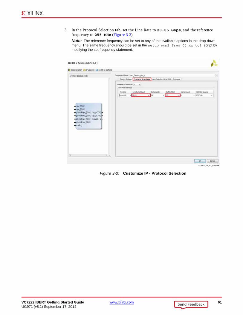
3. In the Protocol Selection tab, set the Line Rate to 28.05 Gbps, and the reference frequency to 255 MHz (Figure 3-3).
Note: The reference frequency can be set to any of the available options in the drop-down menu. The same frequency should be set in the setup_scm2_freq_00_xx.tcl script by modifying the set frequency statement.
X-Ref Target - Figure 3-3
Figure 3-3: Customize IP - Protocol Selection
Send Feedback
62 www.xilinx.com VC7222 IBERT Getting Started GuideUG971 (v5.1) September 17, 2014
Chapter 3: Creating the GTZ IBERT Core
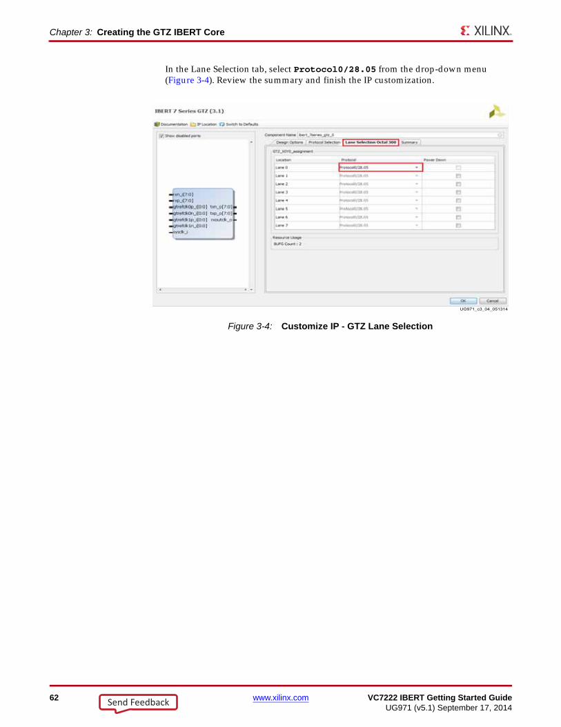
In the Lane Selection tab, select Protocol0/28.05 from the drop-down menu (Figure 3-4). Review the summary and finish the IP customization.
X-Ref Target - Figure 3-4
Figure 3-4: Customize IP - GTZ Lane Selection
Send Feedback

VC7222 IBERT Getting Started Guide www.xilinx.com 63UG971 (v5.1) September 17, 2014
4. Back in the Manage IP window, from the Sources window, right-click the IBERT IP and select Open IP Example Design (Figure 3-5). Specify a location to save the design, press OK, and the design opens in a new Vivado window.
X-Ref Target - Figure 3-5
Figure 3-5: Open IP Example Design
Send Feedback

64 www.xilinx.com VC7222 IBERT Getting Started GuideUG971 (v5.1) September 17, 2014
Chapter 3: Creating the GTZ IBERT Core
5. In the new window select Tools > Run Tcl Script. In the Run Script window, navigate to add_scm2.tcl in the extracted files and press OK. The SuperClock-2 Module Design Sources and Constraints are added to the example design (Figure 3-6).
X-Ref Target - Figure 3-6
Figure 3-6: Sources after Running add_scm2.tcl
Send Feedback
VC7222 IBERT Getting Started Guide www.xilinx.com 65UG971 (v5.1) September 17, 2014
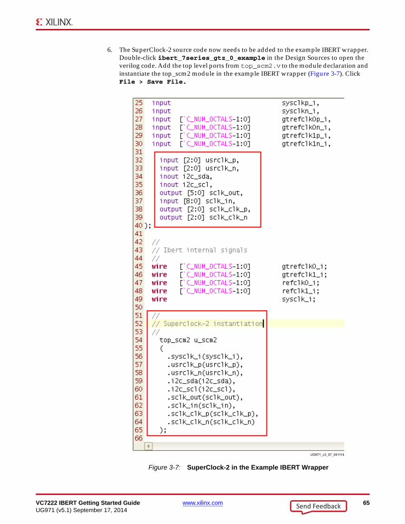
6. The SuperClock-2 source code now needs to be added to the example IBERT wrapper. Double-click ibert_7series_gtz_0_example in the Design Sources to open the verilog code. Add the top level ports from top_scm2.v to the module declaration and instantiate the top_scm2 module in the example IBERT wrapper (Figure 3-7). Click File > Save File.
X-Ref Target - Figure 3-7
Figure 3-7: SuperClock-2 in the Example IBERT Wrapper
Send Feedback

66 www.xilinx.com VC7222 IBERT Getting Started GuideUG971 (v5.1) September 17, 2014
Chapter 3: Creating the GTZ IBERT Core
7. In the Sources window, Design Sources should now reflect that the SuperClock-2 module is part of the example IBERT design (Figure 3-8).
8. Click Run Synthesis in the Flow Navigator, which synthesizes the complete design (Figure 3-9).
X-Ref Target - Figure 3-8
Figure 3-8: Design Sources File Hierarchy
X-Ref Target - Figure 3-9
Figure 3-9: Run Synthesis
Send Feedback
VC7222 IBERT Getting Started Guide www.xilinx.com 67UG971 (v5.1) September 17, 2014
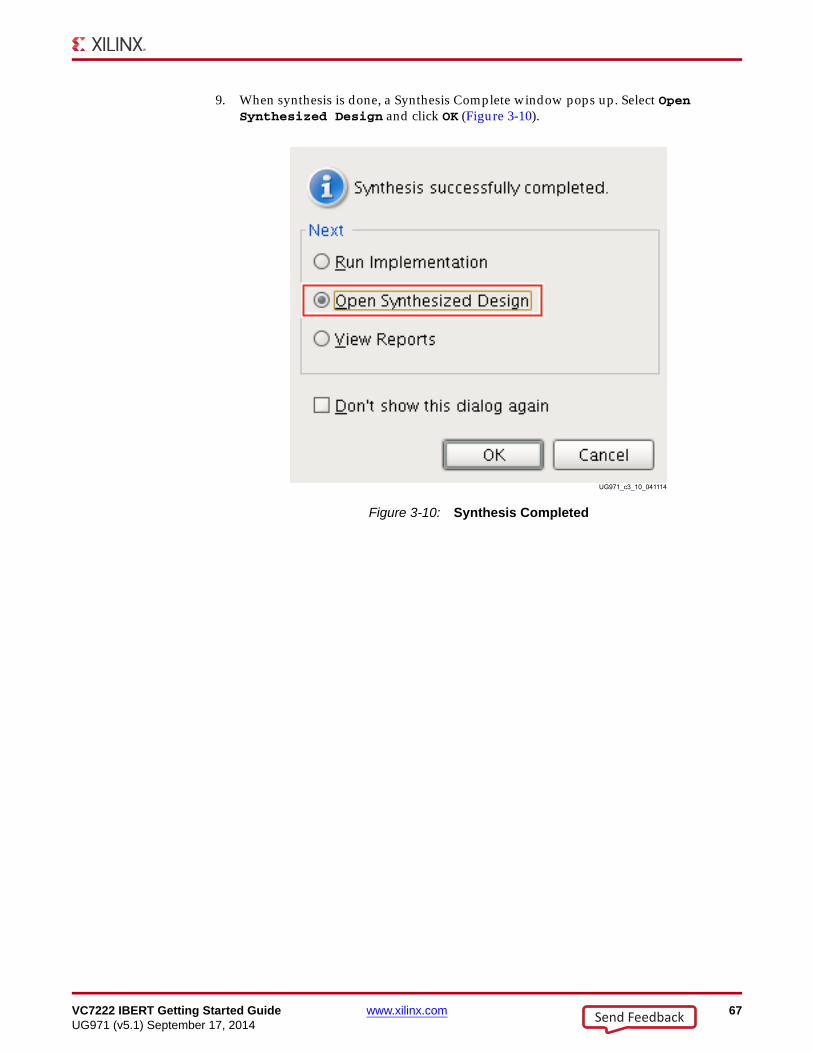
9. When synthesis is done, a Synthesis Complete window pops up. Select Open Synthesized Design and click OK (Figure 3-10).
X-Ref Target - Figure 3-10
Figure 3-10: Synthesis Completed
Send Feedback
68 www.xilinx.com VC7222 IBERT Getting Started GuideUG971 (v5.1) September 17, 2014
Chapter 3: Creating the GTZ IBERT Core
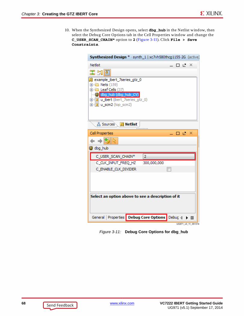
10. When the Synthesized Design opens, select dbg_hub in the Netlist window, then select the Debug Core Options tab in the Cell Properties window and change the C_USER_SCAN_CHAIN* option to 2 (Figure 3-11). Click File > Save Constraints.
X-Ref Target - Figure 3-11
Figure 3-11: Debug Core Options for dbg_hub
Send Feedback
VC7222 IBERT Getting Started Guide www.xilinx.com 69UG971 (v5.1) September 17, 2014
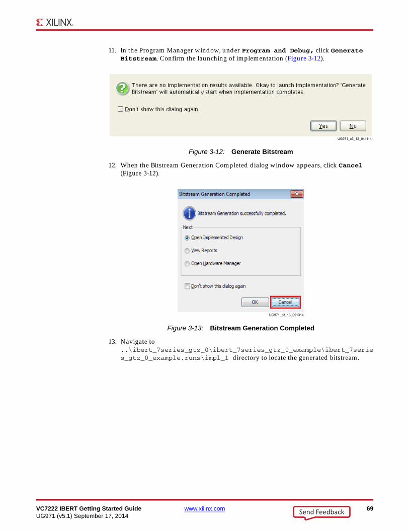
11. In the Program Manager window, under Program and Debug, click Generate Bitstream. Confirm the launching of implementation (Figure 3-12).
12. When the Bitstream Generation Completed dialog window appears, click Cancel (Figure 3-12).
13. Navigate to ..\ibert_7series_gtz_0\ibert_7series_gtz_0_example\ibert_7series_gtz_0_example.runs\impl_1 directory to locate the generated bitstream.
X-Ref Target - Figure 3-12
Figure 3-12: Generate Bitstream
X-Ref Target - Figure 3-13
Figure 3-13: Bitstream Generation Completed
Send Feedback

70 www.xilinx.com VC7222 IBERT Getting Started GuideUG971 (v5.1) September 17, 2014
Chapter 3: Creating the GTZ IBERT Core
Send Feedback
VC7222 IBERT Getting Started Guide www.xilinx.com 71UG971 (v5.1) September 17, 2014
Appendix A
Additional Resources
Xilinx ResourcesFor support resources such as Answers, Documentation, Downloads, and Forums, see the Xilinx Support website.
For continual updates, add the Answer Record to your myAlerts.
Solution CentersSee the Xilinx Solution Centers for support on devices, software tools, and intellectual property at all stages of the design cycle. Topics include design assistance, advisories, and troubleshooting tips.
ReferencesThe most up to date information related to the VC7222 kit and its documentation is available on these websites.
Virtex-7 FPGA VC7222 Characterization Kit
Virtex-7 FPGA VC7222 Characterization Kit documentation
Virtex-7 FPGA VC7222 Characterization Kit Master Answer Record (AR 54015)
These Xilinx documents provide supplemental material useful with this guide:
1. Virtex-7 FPGA VC7222 GTH and GTZ Transceiver Characterization Board User Guide (UG965)
2. HW-CLK-101-SCLK2 SuperClock-2 Module User Guide (UG770)
3. Vivado Design Suite User Guide: Programming and Debugging (UG908)
4. LogiCORE IP Integrated Bit Error Ratio Tester (IBERT) for 7 Series GTH Transceivers Product Guide for Vivado Design Suite (PG152)
5. LogiCORE IP Integrated Bit Error Ratio Tester (IBERT) for 7 Series GTX Transceivers Product Guide for Vivado Design Suite (PG132)
Send Feedback

72 www.xilinx.com VC7222 IBERT Getting Started GuideUG971 (v5.1) September 17, 2014
Appendix A: Additional Resources
Send Feedback

VC7222 IBERT Getting Started Guide www.xilinx.com 73UG971 (v5.1) September 17, 2014
Appendix B
Warranty
THIS LIMITED WARRANTY applies solely to standard hardware development boards and standard hardware programming cables manufactured by or on behalf of Xilinx (“Development Systems”). Subject to the limitations herein, Xilinx warrants that Development Systems, when delivered by Xilinx or its authorized distributor, for ninety (90) days following the delivery date, will be free from defects in material and workmanship and will substantially conform to Xilinx publicly available specifications for such products in effect at the time of delivery. This limited warranty excludes: (i) engineering samples or beta versions of Development Systems (which are provided “AS IS” without warranty); (ii) design defects or errors known as “errata”; (iii) Development Systems procured through unauthorized third parties; and (iv) Development Systems that have been subject to misuse, mishandling, accident, alteration, neglect, unauthorized repair or installation. Furthermore, this limited warranty shall not apply to the use of covered products in an application or environment that is not within Xilinx specifications or in the event of any act, error, neglect or default of Customer. For any breach by Xilinx of this limited warranty, the exclusive remedy of Customer and the sole liability of Xilinx shall be, at the option of Xilinx, to replace or repair the affected products, or to refund to Customer the price of the affected products. The availability of replacement products is subject to product discontinuation policies at Xilinx. Customer may not return product without first obtaining a customer return material authorization (RMA) number from Xilinx.
THE WARRANTIES SET FORTH HEREIN ARE EXCLUSIVE. XILINX DISCLAIMS ALL OTHER WARRANTIES, WHETHER EXPRESS, IMPLIED OR STATUTORY, INCLUDING, WITHOUT LIMITATION, ANY WARRANTY OF MERCHANTABILITY, FITNESS FOR A PARTICULAR PURPOSE, OR NON-INFRINGEMENT, AND ANY WARRANTY THAT MAY ARISE FROM COURSE OF DEALING, COURSE OF PERFORMANCE, OR USAGE OF TRADE. (2008.10)
Do not throw Xilinx products marked with the “crossed out wheeled bin” in the trash. Directive 2002/96/EC on waste electrical and electronic equipment (WEEE) requires the separate collection of WEEE. Your cooperation is essential in ensuring the proper management of WEEE and the protection of the environment and human health from potential effects arising from the presence of hazardous substances in WEEE. Return the marked products to Xilinx for proper disposal. Further information and instructions for free-of-charge return available at: www.xilinx.com\ehs\weee.htm.
Send Feedback

74 www.xilinx.com VC7222 IBERT Getting Started GuideUG971 (v5.1) September 17, 2014
Appendix B: Warranty
Send Feedback

![Jacques IBERT [2010.5.]=Catalogue.pdf](https://static.fdocuments.us/doc/165x107/577c7db01a28abe0549f9507/jacques-ibert20105cataloguepdf.jpg)