
VII. Semiconducting Materials & Devices A.Band Structure and Terminology B.Intrinsic Behavior...
36
VII. Semiconducting Materials & Devices A. Band Structure and Terminology B. Intrinsic Behavior C. Optical Absorption by Semiconductors D. Impurity Conductivity E. Extrinsic Behavior F. Hall Effect and Hall Mobility G. The Diode: A Simple p-n Junction
-
date post
19-Dec-2015 -
Category
Documents
-
view
222 -
download
0
Transcript of VII. Semiconducting Materials & Devices A.Band Structure and Terminology B.Intrinsic Behavior...

VII. Semiconducting Materials & Devices
A. Band Structure and Terminology
B. Intrinsic Behavior
C. Optical Absorption by Semiconductors
D. Impurity Conductivity
E. Extrinsic Behavior
F. Hall Effect and Hall Mobility
G. The Diode: A Simple p-n Junction

A. Band Structure and Terminology Semiconductors and insulators have qualitatively similar band structures, with the quantitative distinction that the band gap Eg > 3.0 eV in insulators.
conduction band
valence band
Energy band diagram in k-space “Flat-band” diagram in real space
Ec = conduction band edge
Ev = valence band edge

Fermi-Dirac Distribution FunctionThe important external parameter that determines the properties of a semiconductor is the temperature T, which controls the excitation of electrons across the band gap in a pure (intrinsic) semiconductor.
1
1)(
/)( kTe
Ef
Fermi-Dirac distribution function
The probability for an electron to be in an energy level at temperature T
= chemical potential EF for T << TF
For nearly all T of interest: kT )(
kTeEf /)()( So we can approximate:This is the Maxwell-Boltzmann (classical) limit of Fermi-Dirac statistics

B. Intrinsic Behavior “Intrinsic” means without impurities. Electrical conductivity is zero at T = 0, but for T > 0 some electrons are excited into the conduction band, also creating holes (H+) in the valence band. In general the conductivity can be written (using the nearly FEG model):
h
h
e
e
m
pe
m
ne 22
The conductivity is controlled by the magnitude of n and p, which rise exponentially as T increases. The relaxation times are only dependent on 1/T, and this dependence is often ignored because the exponential behavior dominates.
Experimentally we find that for a pure semiconductor:
high-T (intrinsic) region
low-T (extrinsic) region
as T due to increased scattering ( )

Intrinsic Carrier Statistics It is relatively simple to calculate n(T) and p(T) for the intrinsic region, where the conductivity is caused by excitation of e- across the energy gap:
e- in the conduction band:
h+ in the valence band:Ev = 0
Ec = Eg
eg m
kEE
2
2
hm
kE
2
2
For parabolic bands the density of states are: 2/1
2/3
22
2
2)( g
en EE
mVEN
02
2)( 2/1
2/3
22
EEmV
EN hh
Think: why are we justified in assuming parabolic E(k) here?
Intrinsic Carrier Statistics, cont’d.
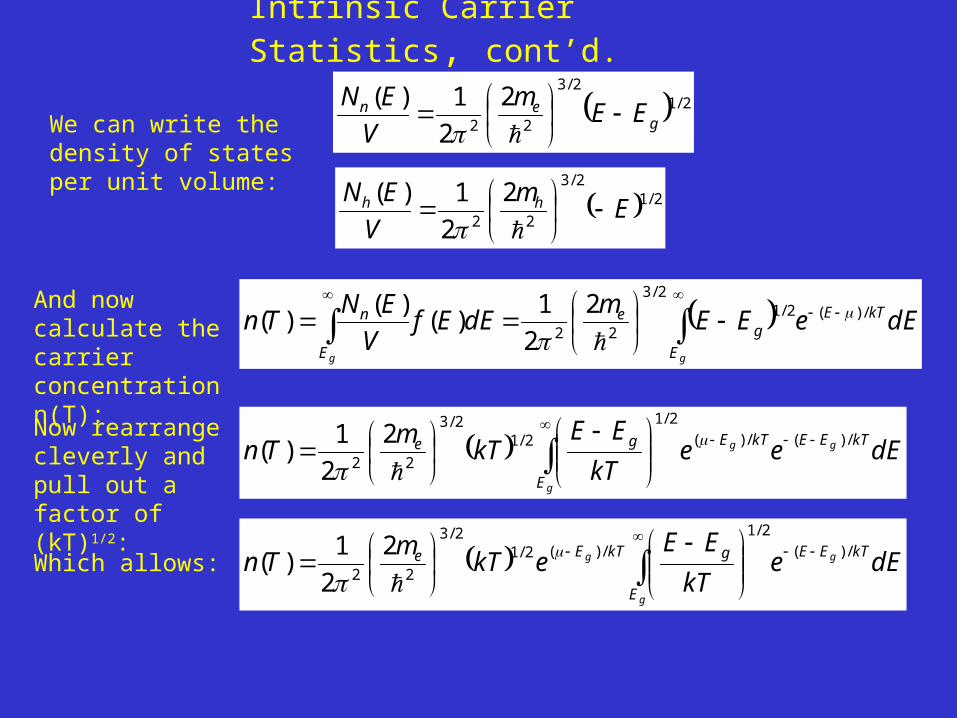
We can write the density of states per unit volume:
And now calculate the carrier concentration n(T):
dEeEEm
dEEfV
ENTn kTE
E
ge
E
n
gg
/)(2/12/3
22
2
2
1)(
)()(
2/12/3
22
2
2
1)(E
m
V
EN hh
Now rearrange cleverly and pull out a factor of (kT)1/2:
2/12/3
22
2
2
1)(g
en EEm
V
EN
dEeekT
EEkT
mTn kTEE
E
kTEge g
g
g /)(/)(
2/1
2/12/3
22
2
2
1)(
Which allows: dEekT
EEekT
mTn kTEE
E
gkTEe g
g
g /)(
2/1
/)(2/12/3
22
2
2
1)(
Intrinsic Carrier Statistics, cont’d.
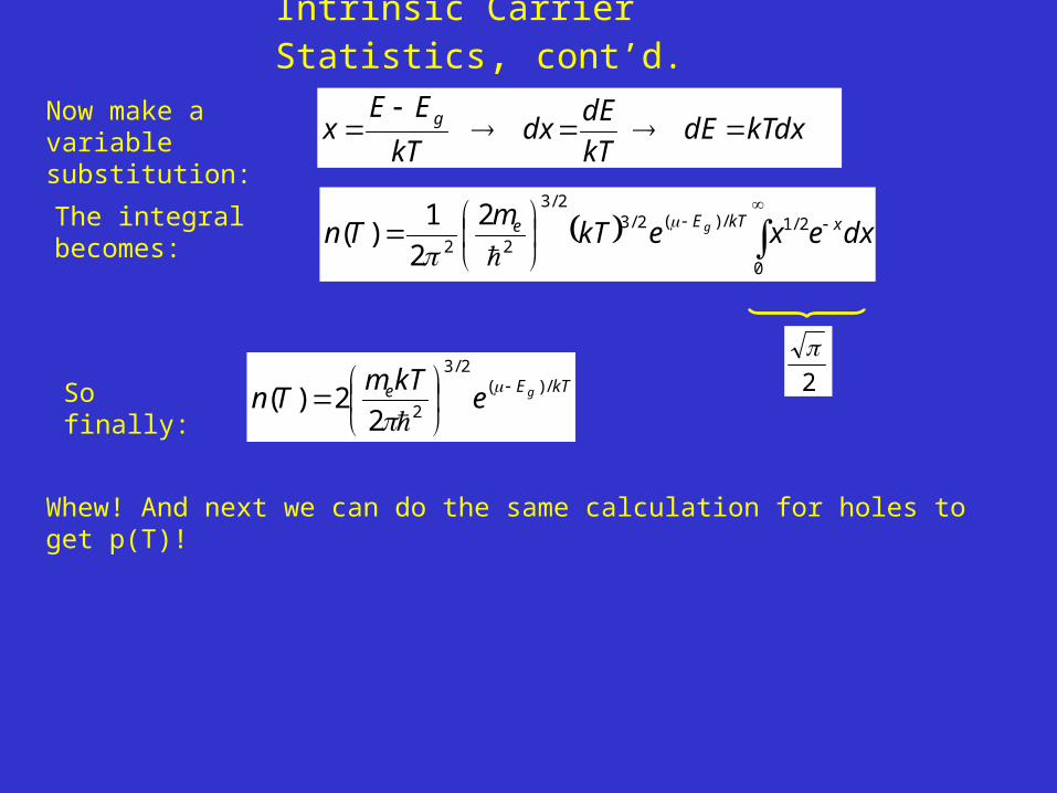
Now make a variable substitution:
Whew! And next we can do the same calculation for holes to get p(T)!
kTdxdEkT
dEdx
kT
EEx g
dxexekTm
Tn xkTEe g
0
2/1/)(2/32/3
22
2
2
1)(
The integral becomes:
2
So finally: kTEe gekTm
Tn /)(2/3
222)(
Intrinsic Hole Carrier Statistics
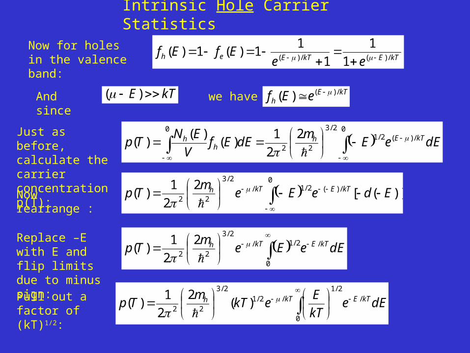
Now for holes in the valence band:
Just as before, calculate the carrier concentration p(T):
dEeEm
dEEfV
ENTp kTEh
hh /)(
02/1
2/3
22
0 2
2
1)(
)()(
Now rearrange :
Pull out a factor of (kT)1/2:
kTEkTEeh eeEfEf
/)(/)( 1
1
1
11)(1)(
kTE )(And since kTEh eEf /)()( we have
)]([2
2
1)( /)(
02/1/
2/3
22EdeEe
mTp kTEkTh
Replace –E with E and flip limits due to minus sign:
dEeEem
Tp kTEkTh /
0
2/1/2/3
22
2
2
1)(
dEekT
EekT
mTp kTEkTh /
0
2/1/2/1
2/3
22)(
2
2
1)(
Intrinsic Hole Carrier Statistics, cont’d.
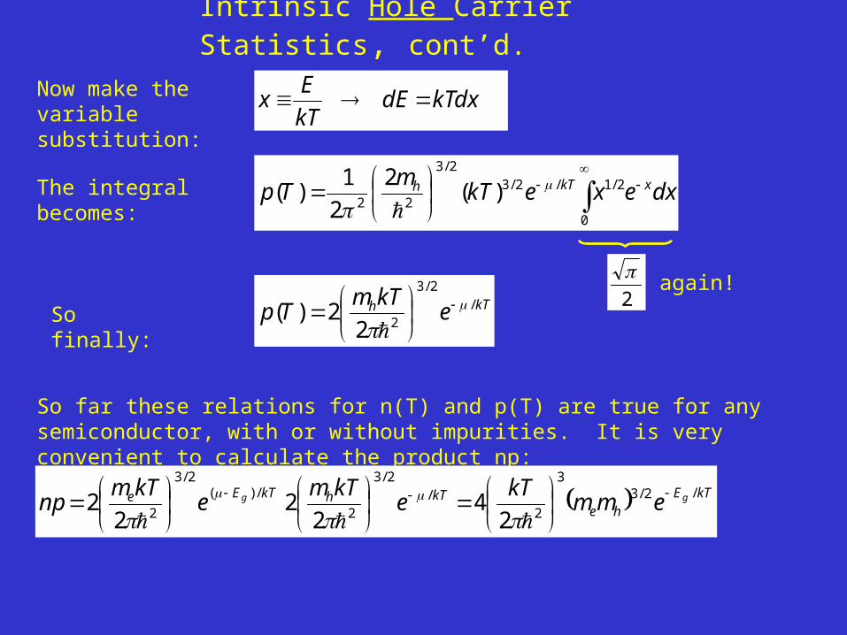
So far these relations for n(T) and p(T) are true for any semiconductor, with or without impurities. It is very convenient to calculate the product np:
Now make the variable substitution:
kTdxdEkT
Ex
So finally:kTh e
kTmTp /
2/3
222)(
2
again!
dxexekTm
Tp xkTh
0
2/1/2/32/3
22)(
2
2
1)(
The integral becomes:
kTEhe
kThkTEe gg emmkT
ekTm
ekTm
np /2/33
2/
2/3
2
/)(2/3
2 24
22
22

Intrinsic Carrier Statistics: Results
Now for an intrinsic semiconductor (or in the intrinsic region of a doped semiconductor) ni = pi, so:
And equating the earlier expressions for n and p:
kTEheii
gemmkT
pn 2/4/32/3
222
kThkTEe ekTm
ekTm g /
2/3
2
/)(2/3
2 22
22
2/3
/)2(
e
hkTE
m
me g
This gives an expression for (T):
e
hg
e
hg m
mkTE
m
mkTE ln
4
3
2
1ln
22
12/3
2/3
ln2
e
hg
m
m
kT
E
So the chemical potential, or Fermi level, has some dependence on T, but if mh and me are similar, then this is very small.

Carrier Mobility
The total conductivity, including both the electron and hole contributions, is:
It is common to define a quantity that expresses the size of the drift speed for each type of carrier in an electric field E:
Em
ev
Earlier FEG result:
h
h
e
e
m
pe
m
ne 22
Definition of carrier mobility: i
ii m
e
E
v
Now we can rewrite the total conductivity as: he pene
(Note: the carrier mobility is directly related to the switching speed of a solid-state electronic device)
Experiment shows that has a power-law temperature dependence: 22 nT n
So a plot of vs. 1/T gives a straight line with slope –Eg/2k. Conductivity measurements allow us to determine Eg!
kTEi
gAe 2/Thus the exponential temperature dependence of n and p dominates, and we can approximate the intrinsic conductivity
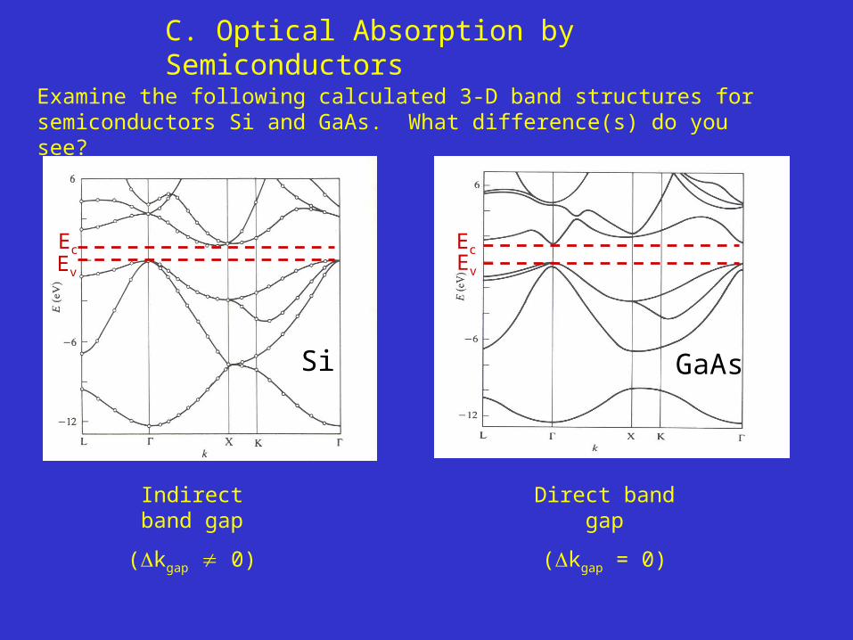
C. Optical Absorption by Semiconductors
Examine the following calculated 3-D band structures for semiconductors Si and GaAs. What difference(s) do you see?
Indirect band gap
(kgap 0)
Direct band gap
(kgap = 0)
Si GaAs
Ev
EcEv
Ec
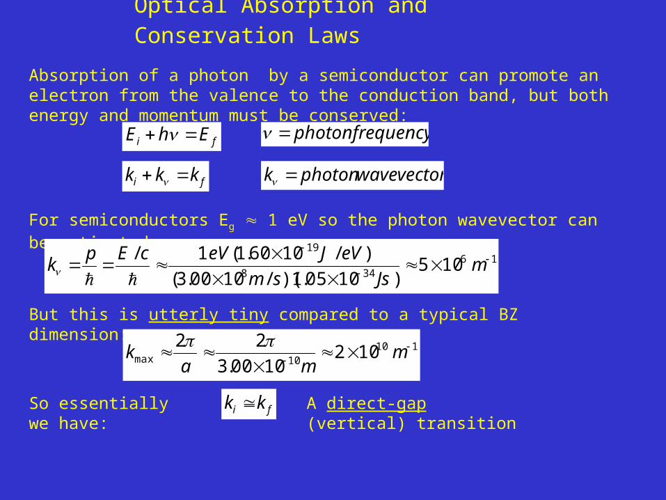
Optical Absorption and Conservation Laws
Absorption of a photon by a semiconductor can promote an electron from the valence to the conduction band, but both energy and momentum must be conserved:
fi EhE frequencyphoton
fi kkk
wavevectorphotonk
For semiconductors Eg 1 eV so the photon wavevector can be estimated:
But this is utterly tiny compared to a typical BZ dimension:
So essentially we have: fi kk
A direct-gap (vertical) transition
16348
19
105)1005.1)(/1000.3(
)/1060.1(1/
m
Jssm
eVJeVcEpk
11010max 102
1000.3
22
m
mak
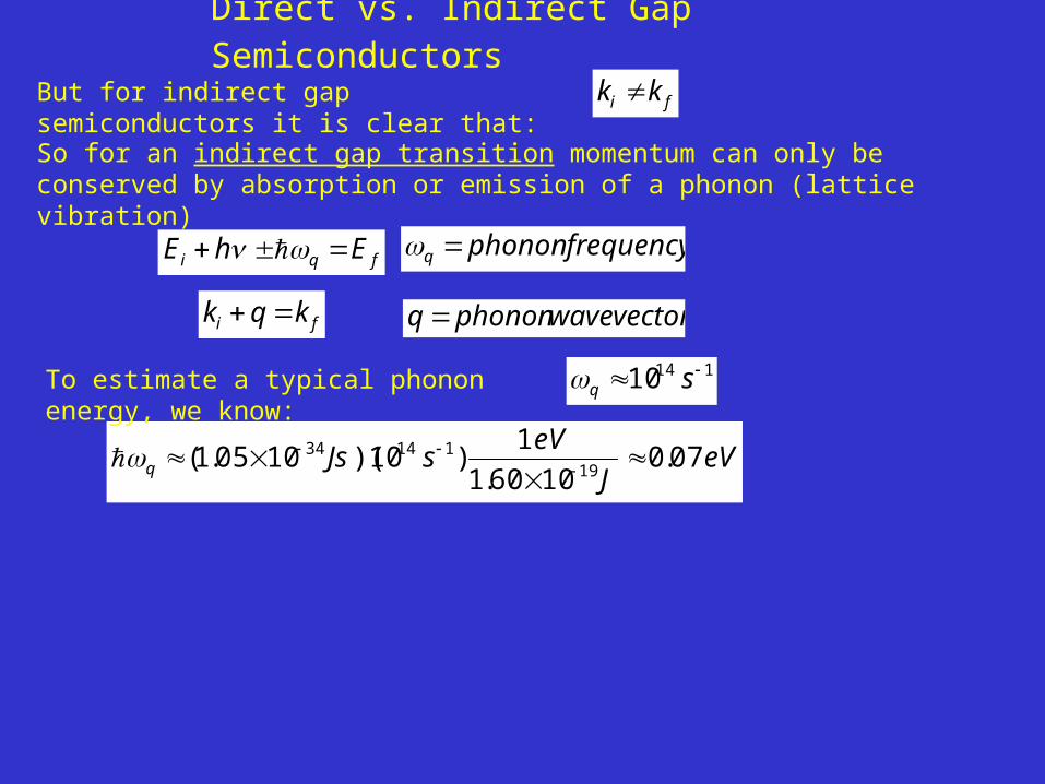
Direct vs. Indirect Gap Semiconductors
fqi EhE frequencyphononq
fi kqk
wavevectorphononq
But for indirect gap semiconductors it is clear that: fi kk
eVJ
eVsJsq 07.0
1060.1
1)10)(1005.1(
1911434
So for an indirect gap transition momentum can only be conserved by absorption or emission of a phonon (lattice vibration)
To estimate a typical phonon energy, we know: 11410 sq

Optical Absorption: Experimental Results Experimental absorption coefficients () are measured to be:
2/1gd EhA
While for an indirect gap material with a direct transition at a slightly higher energy:
2)()( gi EhTAT
gE h
d i
hqgE
i
hqgE 2E

D. Impurity Conductivity in Semiconductors Consider two types of substitutional impurities in Si:
pure Si:
(each line represents
an e-)
Si:P
Si:B
weakly bound extra electron
missing electron
donor energy level(n-type material)
acceptor energy level(p-type material)
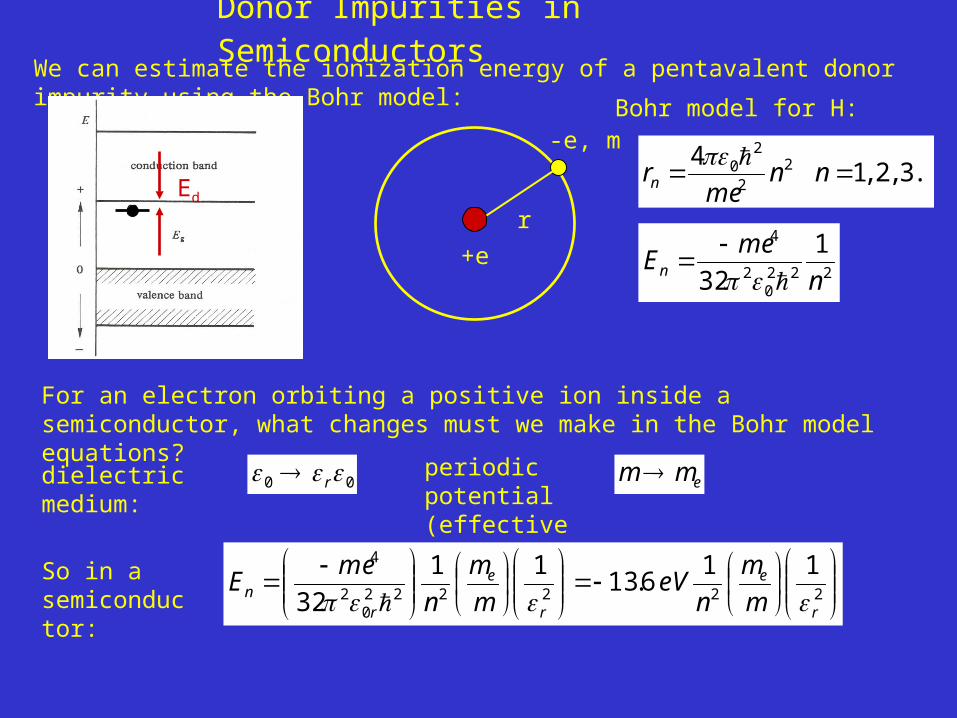
Donor Impurities in Semiconductors We can estimate the ionization energy of a pentavalent donor impurity using the Bohr model:
Bohr model for H:
For an electron orbiting a positive ion inside a semiconductor, what changes must we make in the Bohr model equations?
Ed
+e
-e, m
r
...3,2,14 2
2
20 nn
mern
2220
2
4 1
32 n
meEn
dielectric medium: periodic potential (effective mass):
00 r emm
2222220
2
4 116.13
11
32 r
e
r
e
rn m
m
neV
m
m
n
meE
So in a semiconductor:

Donor Ionization Energy Assuming that the electron is initially in its lowest energy level, the donor ionization energy Ed is:
Experimental data reveal ionization energies (in meV):
For Si we can use representative values of the effective mass and dielectric constant to obtain:
All within a factor of two of our rough estimate!
The orbital radius is predicted to be:
2221
16.13
1
1
16.130
r
e
r
ed m
meV
m
meVEEE
eVeVEd 026.08.11
126.06.13
2
P As Sb
Si 45 49 39
oo
rem
m
mer
248.11
26.0
1529.01
4 22
20
1
So this electron moves through a region that includes hundreds of atoms, which supports the use of the dielectric constant of the bulk semiconductor.

Acceptor Impurities in Semiconductors What happens when the impurity atom is trivalent?
At 0 K the acceptor level is empty, so a “hole” is bound to the impurity atom.
However, the energy Ea is so small (50 meV in Si) that at room T electrons in the valence band bound to other Si atoms can be excited into the acceptor level, leaving behind a mobile hole in the valence band.
Summary: Both donor (P, As) and acceptor (B, Ga) impurities provide an easy way to increase either n or p even at low T. When such impurity-related carriers dominate the electrical properties, the semiconductor material displays extrinsic behavior.
Ea
Note: If impurity concentration is very large, the Bohr orbits (wavefunctions) of the donor electrons can overlap and form an “impurity band” that extends throughout the material. This leads to a so-called insulator-metal transition and causes an abrupt increase in the conductivity (see problem 10.5).

E. Extrinsic Behavior and StatisticsLet’s consider donor impurities in a semiconductor (n-type):
0ddd NNN
Now in the presence of a large donor e- concentration, then n >> ni so p must decrease in order to keep the product np = constant. What physical process causes p to decrease?
Nd+ = concentration of ionized donor atoms
Nd0 = concentration of neutral donor atoms
Nd = concentration of donor atoms
Essentially the large number of e- in the conduction band will be sufficient to fill most available holes in the valence band, so that:
d
Nn np and
0)(0 ddgddEEEfNN
1/)(0
kTEE
dd dge
NN Ev = 0
Eg
Eg-Ed
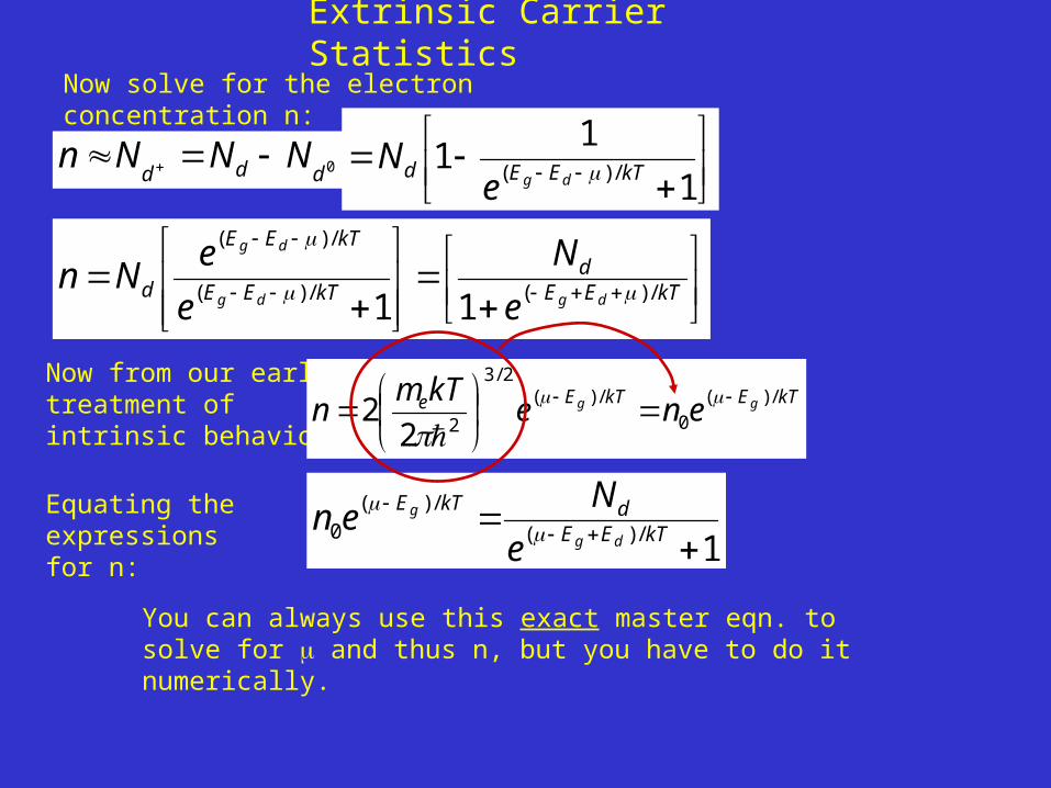
Extrinsic Carrier StatisticsNow solve for the electron concentration n:
Now from our earlier treatment of intrinsic behavior:
0dddNNNn
1
11 /)( kTEEd dge
N
kTEEd
kTEE
kTEE
d dgdg
dg
e
N
e
eNn /)(/)(
/)(
11
kTEkTEe gg enekTm
n /)(0
/)(2/3
222
Equating the expressions for n: 1/)(
/)(0
kTEE
dkTE
dg
g
e
Nen
You can always use this exact master eqn. to solve for and thus n, but you have to do it numerically.

Limits of Low and High Impurity ConcentrationsThis discussion is relevant to several HW problems in Myers (see 10.4, 10.8, 10.9). It provides simple approximations for n and corresponding to very small Nd and very large Nd.
We will develop approximations to simplify the solution of this eqn.
Ev = 0
Eg
Now consider two extreme limiting cases:
1/)(
/)(0
kTEE
dkTE
dg
g
e
Nenn
1. Nd << n0 In Si at 300K (high T limit)
ge
hg E
m
mkTE
2
1ln
4
3
2
1
Since Eg >> 2kT at room temp, this means 1/)( kTEE dge
Thus, ddkTE N
Nenn g
1/)(
0
3242/3
20 104.32
2
m
kTmn e
And solving for :
0
lnn
NkTE d
g
)2/(/)(/)( 21 kTEkTEEkTEE gdgdg eee
Limits of Low and High Impurity Concentrations
And now solve for :
kTEEd
kTEEdkTE
dgdg
g
e
N
e
Nenn /)(/)(
/)(0
1
kTEkTEEkTEEddddg eee 2//)(/)(
21
Thus,
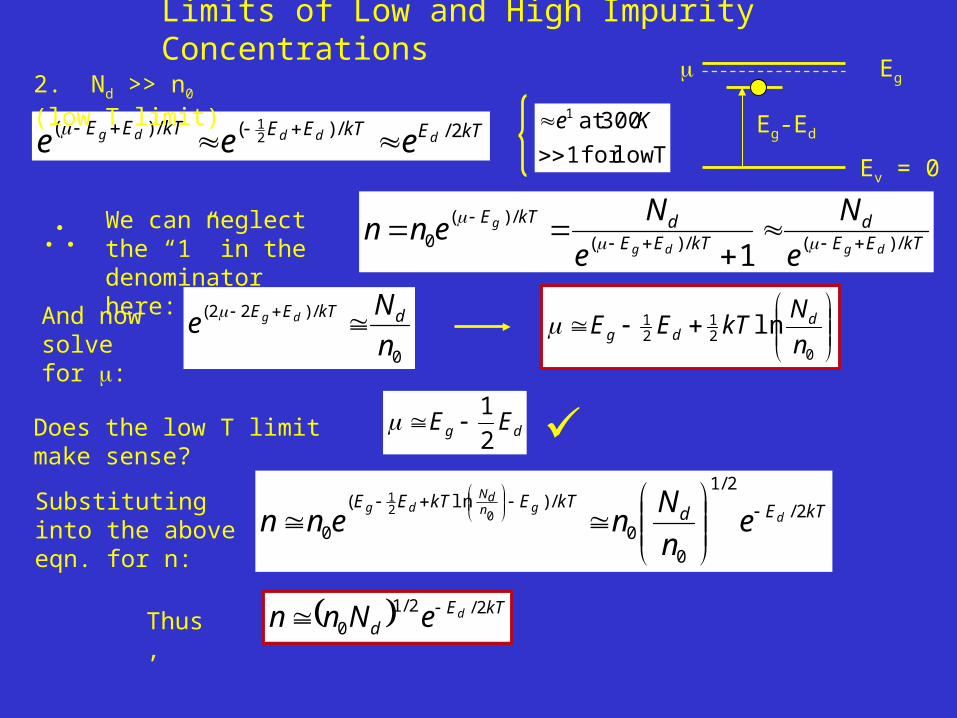
2. Nd >> n0 (low T limit)
Ev = 0
Eg
Eg-Ed
Tlowfor1
300at1
Ke
We can neglect the “1” in the denominator here:
0
/)22(
n
Ne dkTEE dg
021
21 ln
n
NkTEE d
dg
Substituting into the above eqn. for n:
kTEdkTEkTEE
dgn
dNdg
en
Nnenn 2/
2/1
00
/)ln(
002
1
kTEd
deNnn 2/2/10
Does the low T limit make sense? dg EE2
1

Summary of Impurity Semiconductor Behavior
Now our schematic plot of ln vs. 1/T is even easier to understand:
kTEin
ge 2/
kTEex
de 2/
constant dNn
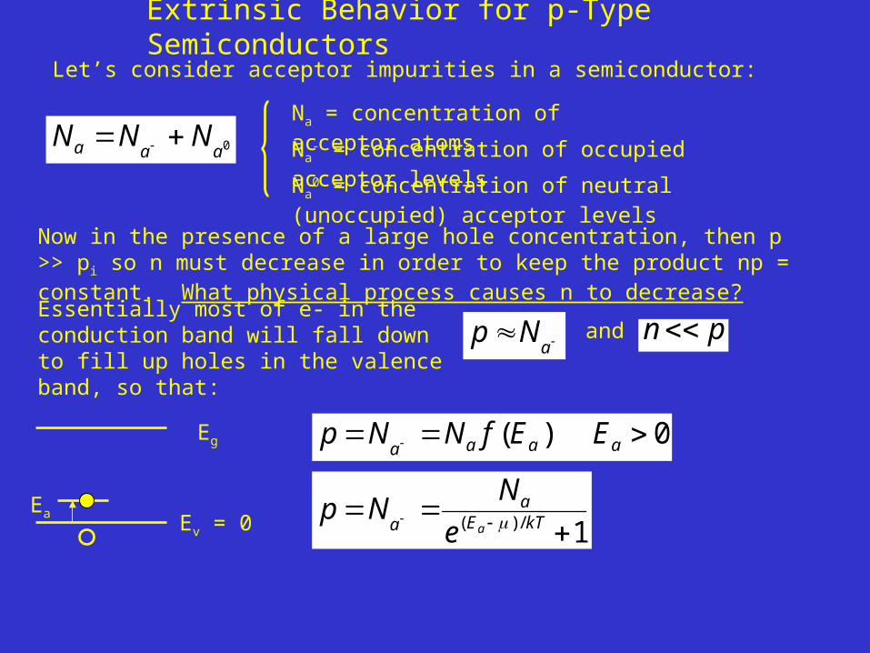
Extrinsic Behavior for p-Type SemiconductorsLet’s consider acceptor impurities in a semiconductor:
0aaa NNN
Now in the presence of a large hole concentration, then p >> pi so n must decrease in order to keep the product np = constant. What physical process causes n to decrease?
Na- = concentration of occupied acceptor levels
Na0 = concentration of neutral (unoccupied) acceptor levels
Na = concentration of acceptor atoms
Essentially most of e- in the conduction band will fall down to fill up holes in the valence band, so that:
a
Np pn and
0)( aaaaEEfNNp
1/)( kTE
aa ae
NNp Ev = 0
Eg
Ea

Extrinsic p-Type Carrier Statistics
Now from our earlier treatment of intrinsic behavior:
kTkTh epekTm
p /0
/2/3
222
Again, you can always use this exact master eqn. to solve for and thus p, but you have to do it numerically.
Equating the expressions for p: 1/)(
/0
kTEakT
ae
Nep
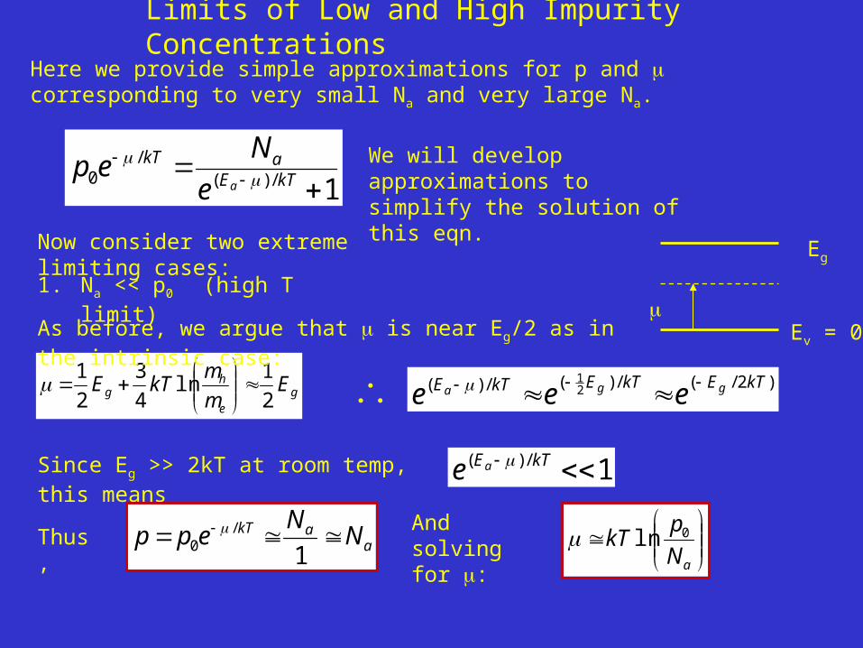
Limits of Low and High Impurity ConcentrationsHere we provide simple approximations for p and corresponding to very small Na and very large Na.
We will develop approximations to simplify the solution of this eqn.
Ev = 0
Eg
Now consider two extreme limiting cases:
1. Na << p0 (high T limit)
ge
hg E
m
mkTE
2
1ln
4
3
2
1
Since Eg >> 2kT at room temp, this means 1/)( kTEae
Thus, aakT N
Nepp
1/
0 And solving
for :
aN
pkT 0ln
)2/(/)(/)( 21 kTEkTEkTE gga eee
1/)(/
0
kTEakT
ae
Nep
As before, we argue that is near Eg/2 as in the intrinsic case:

Limits of Low and High Impurity Concentrations
And now solve for :
kTEa
kTEakT
aa e
N
e
Nepp /)(/)(
/0 1
kTEkTEEkTE aaaa eee 2//)(/)( 21
Thus,
2. Na >> p0 (low T limit)
Ev = 0
Eg
Ea Tlowfor1
300at1
Ke
We can neglect the “1” in the denominator here:
0
/)2(
p
Ne akTEa
021
21 ln
p
NkTE a
a
Substituting into the above eqn. for p:
kTE
a
kTkTEaaN
pa
eN
ppepp 2/
2/1
00
/)ln(
0
021
21
kTEa
aeNpp 2/2/10
Does the low T limit make sense? aE2
1
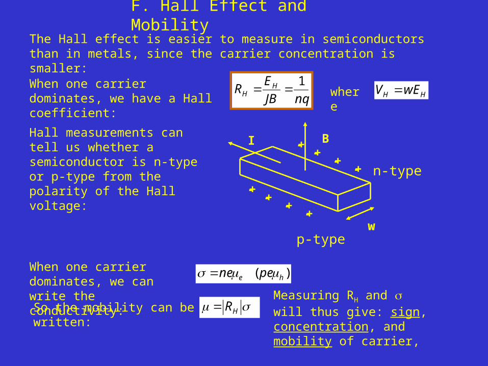
F. Hall Effect and MobilityThe Hall effect is easier to measure in semiconductors than in metals, since the carrier concentration is smaller:
Hall measurements can tell us whether a semiconductor is n-type or p-type from the polarity of the Hall voltage:
nqJB
ER HH
1When one carrier dominates, we have
a Hall coefficient: HH wEV where
BI
w
--
--
++
++
++
++
--
-- n-type
p-type
When one carrier dominates, we can write the conductivity:
)( he pene
So the mobility can be written: HRMeasuring RH and will thus give: sign, concentration, and mobility of carrier,

General Form of Hall Coefficient
For a semiconductor with significant concentrations of both types of carriers:
)(
22
he
ehHH pne
np
JB
ER
So if holes predominate (ph > ne ), RH > 0 and the material is said to be p-type, while if RH < 0 (as for simple metals), the material is said to be n-type.

G. The Diode: A Simple p-n JunctionWhen p- and n-type materials are fabricated and brought together to form a junction, we can easily analyze its electronic properties.
p n
NaNd
Near the junction the free electrons and holes “diffuse” across the junction due to the concentration gradients there. As this happens, a contact potential develops.
p n----
++++
E
The field E due to the contact potential inhibits further flow of electrons and holes toward the junction, and equilibrium is established at finite .
depletion region
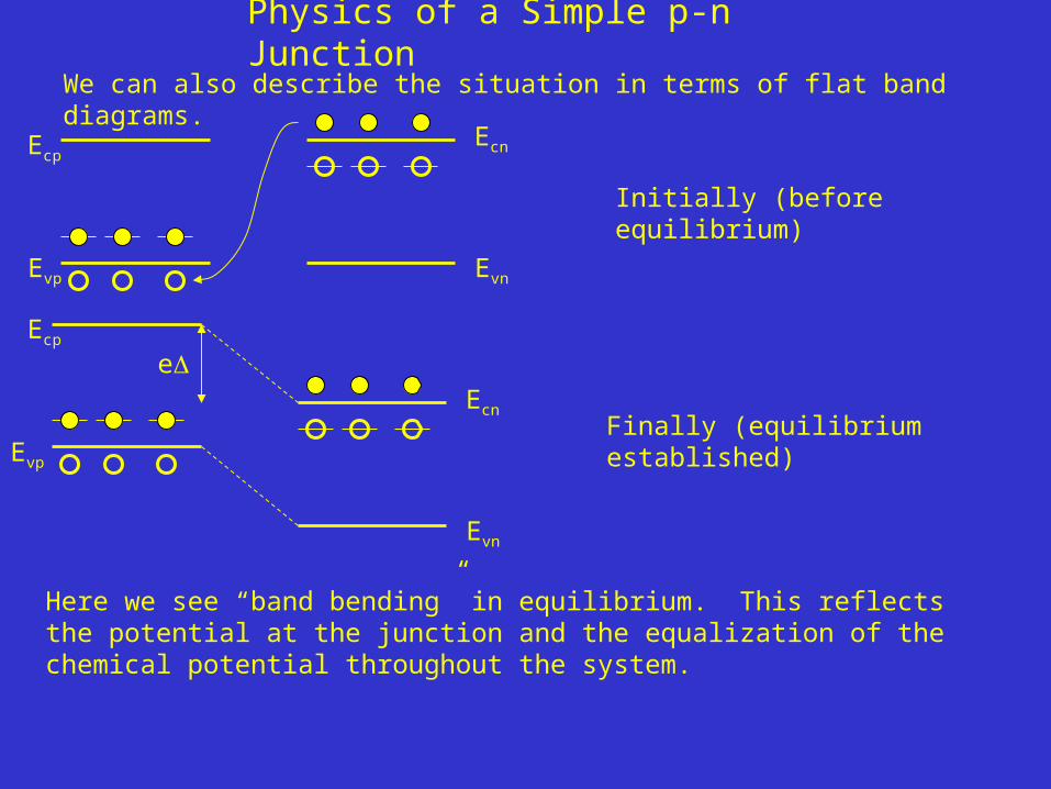
Physics of a Simple p-n JunctionWe can also describe the situation in terms of flat band diagrams.
Initially (before equilibrium)
Finally (equilibrium established)
Ecp
Evp
Ecn
Evn
Ecn
Evn
Ecp
Evp
e
Here we see “band bending” in equilibrium. This reflects the potential at the junction and the equalization of the chemical potential throughout the system.

Physics of a Simple p-n JunctionIn this dynamic equilibrium two types of carrier fluxes are equal and opposite:
1. recombination flux: electrons in the n-type region and holes in the p-type region “climb” the barrier, cross the junction, and recombine with h+/e- on the other side.
2. generation flux: thermally-generated electrons in the p-type region and holes in the n-type region are “swept” across the junction by the built-in electric field there.
We can picture the carrier fluxes (currents):In equilibrium at V=0:
0)0()0( ngnr JJ
0)0()0( pgpr JJ
Jng
Jnr
Jpr
Jpg
p-type
n-type

A Simple p-n Junction With Applied VoltageNow when an external voltage V is applied to the junction, there are two cases:
1. Forward bias: electrons in the n-type region are shifted upward in energy
Generation currents are not affected since they depend on excitation across band gap:
)0()0()( nrngfng JJVJ e
eV
)0()0()( prpgfpg JJVJ
Recombination currents are increased by a Boltzmann factor, since they depend on carriers climbing the potential energy step at the junction (and Maxwell-Boltzmann statistics applies):
kTeVnrfnr eJVJ /)0()(
kTeVprfpr eJVJ /)0()(
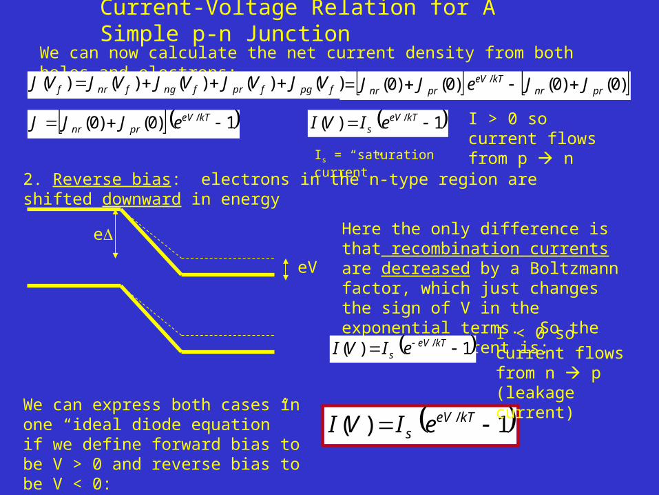
Current-Voltage Relation for A Simple p-n JunctionWe can now calculate the net current density from both holes and electrons:
)0()0()0()0( /prnr
kTeVprnr JJeJJ
e
eV
)()()()()( fpgfprfngfnrf VJVJVJVJVJ
1)0()0( / kTeVprnr eJJJ I > 0 so current
flows from p n
2. Reverse bias: electrons in the n-type region are shifted downward in energy
Here the only difference is that recombination currents are decreased by a Boltzmann factor, which just changes the sign of V in the exponential terms. So the resulting current is:
1)( / kTeVs eIVI
1)( / kTeVs eIVI
I < 0 so current flows from n p (leakage current)
We can express both cases in one “ideal diode equation” if we define forward bias to be V > 0 and reverse bias to be V < 0:
1)( / kTeVs eIVI
Is = “saturation current”
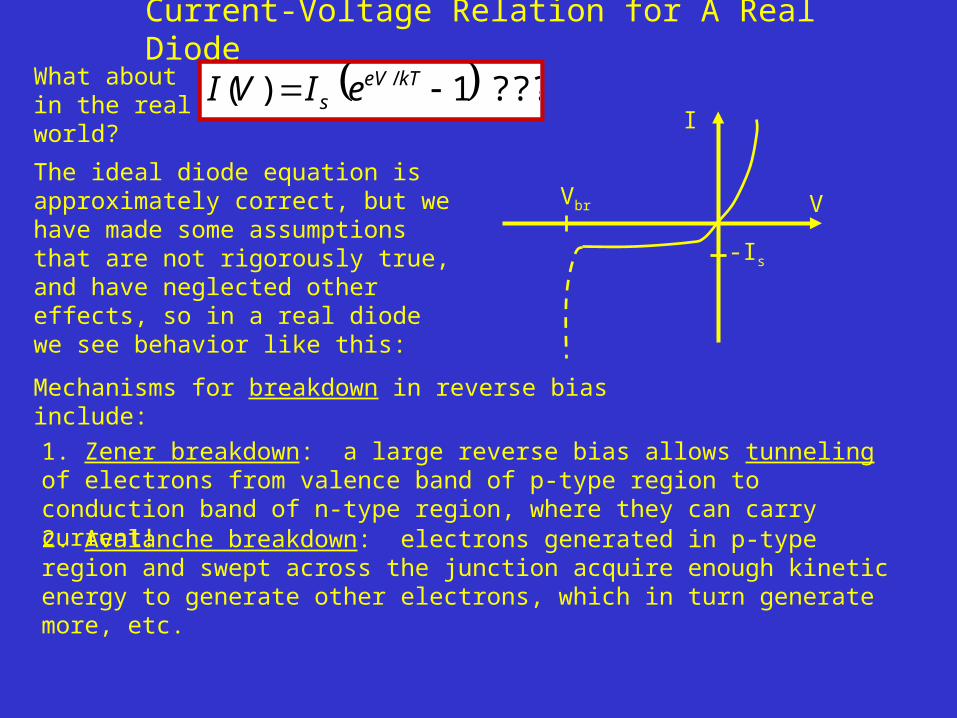
Current-Voltage Relation for A Real DiodeWhat about in the real world?
The ideal diode equation is approximately correct, but we have made some assumptions that are not rigorously true, and have neglected other effects, so in a real diode we see behavior like this:
???1)( / kTeVs eIVI
Mechanisms for breakdown in reverse bias include:
I
V
-Is
Vbr
1. Zener breakdown: a large reverse bias allows tunneling of electrons from valence band of p-type region to conduction band of n-type region, where they can carry current!
2. Avalanche breakdown: electrons generated in p-type region and swept across the junction acquire enough kinetic energy to generate other electrons, which in turn generate more, etc.


![The Effects of Crystallinity on Charge Transport and the ... organic electronic devices.[1–7] As with traditional inorganic semiconductors, the electronic properties of semiconducting](https://static.fdocuments.us/doc/165x107/5ec5127ae474e37cf712acf8/the-effects-of-crystallinity-on-charge-transport-and-the-organic-electronic.jpg)
