Cell Theory Chapter 3 Biology Mr. Gilbertson Hooke’s microscope.

Multifunctional semiconductor micro-Hall devices for
magnetic, electric and photo-detection
A. M. Gilbertson,1 Hatef Sadeghi,2 V. Panchal,3 O. Kazakova,3 C. J. Lambert,2 S. A. Solin,1,4 L. F. Cohen1
1Blackett Laboratory, Imperial College London, Prince Consort Road, London SW7 2BZ, UK2Department of Physics, Lancaster University, Lancaster LA1 4YB, UK
3National Physical Laboratory, Teddington, TW11 0LW, UK4Department of Physics and Institute for Materials Science and Engineering, Washington University in St.
Louis, St Louis, Missouri 63130, USA
ABSTRACT
We report the real-space voltage response of InSb/AlInSb micro-Hall devices to local photo-
excitation, electric, and magnetic fields at room temperature using scanning probe microscopy. We
show that the ultrafast generation of localised photocarriers result in conductance perturbations
analogous to those produced by local electric fields. Experimental results are in good agreement with
tight-binding transport calculations in the diffusive regime. The magnetic, photo and charge
sensitivity of a 2 m wide probe are evaluated at a 10 A bias current in the Johnson noise limit
(valid at measurement frequencies > 10 kHz) to be, respectively; 500 nT/Hz; 20 pW/Hz ( = 635
nm) comparable to commercial photoconductive detectors; and 0.05 e/Hz comparable to that of
single electron transistors. These results demonstrate the remarkably versatile sensing attributes of
simple semiconductor micro-Hall devices that can be applied to a host of imaging and sensing
applications.
[1]

Multifunctional mesoscopic sensors capable of detecting local magnetic, electric, and optical
fields can greatly facilitate image capture in nano-arrays that address a multitude of disciplines
spanning information storage to medical biosensing. While the magnetic sensing attributes of micro-
Hall devices based on high mobility 2D electron gas (2DEG) systems are well known,1,2 the
sensitivity of the transverse voltage output to local electric fields (in zero magnetic field) has only
recently been investigated, and shows the capability for detecting single electron charges3-5. In this
letter we study the real-space voltage response and sensitivity of InSb 2DEG micro-Hall devices to
local electric (E) field, magnetic (B) field and photo-excitation, at room temperature (RT) using
electrical and magnetic scanning gate microscopy (SGM), and scanning photovoltage microscopy
(SPVM), respectively. SGM and SPVM have been used by numerous groups to study local transport
phenomena in buried semiconductor 2DEG nanostructures. In particular, the high spatial resolution
afforded by the SGM technique has been successfully applied to visualise coherent electron flow from
quantum point contacts.6,7 Meanwhile, SPVM experiments have focused primarily on the quantum
Hall regime to visualise edge channel transport at the sample boundaries.8,9 Recently, SPVM has been
used to image ballistic photocurrents10 , spin-dependent transverse photovoltages11 and metal-
semiconductor interface effects12,13 in GaAs-based microstructures. Meanwhile, InSb 2DEG structures
are particularly well suited to sensing applications due to the high RT electron mobility14,15 of e < 60
000 cm2/Vs, exceeded only by that in suspended/encapsulated graphene16. Here we show that micro-
Hall devices exhibit a distinctive photoresponse analogous to their E-field response, due to the
equivalence of the local conductivity perturbations on the current distribution in the vicinity of
voltage leads. Experimental results are well described by calculations in the diffusive transport
regime. In addition to exhibiting excellent magnetic sensitivity, we demonstrate that micro-Hall
devices exhibit a remarkable charge and photo-sensitivity. These results demonstrate the versatile
multifunctional sensing attributes of the simplest 2DEG Hall devices.
The samples studied are fabricated from a modulation doped InSb/AlxIn1-xSb quantum well
(QW) heterostructure grown by molecular beam epitaxy on a semi-insulating GaAs (001) substrate.
The 2DEG is located in a 15 nm thick InSb QW buried 50 nm beneath the surface with an AI0.2In0.8Sb
top cap. Further details of the layer structure are given elsewhere.17 Micro-Hall cross structures with
lateral dimensions (w) varying between 1 μm and 4 μm were fabricated using e-beam lithography and
shallow (≈ 150 nm etch depth) reactive ion etching in a CH4/H2 gas mixture. Cr/Au Ohmic contacts to
the InSb 2DEG were formed using a subtractive etch technique.17 Here, we focus on the results from a
w = 2 μm Hall cross structure (SPVM and SGM data from a 1 μm and 4 μm device are presented in
supplemental material18). The RT electrical transport properties of the devices are characterised by an
electron density n0 = 5 x 1011 cm-2, e = 34,000 cm2/Vs and resistivity ρ0 = 367 /, as determined by
conventional magnetotransport measurements.
[2]

All measurements presented were performed at RT under ambient conditions with a constant
DC bias current I0 applied across the device. In the SPVM measurement samples are optically excited
using a = 635 nm cw diode laser. The light is mechanically chopped at 512 Hz and focused onto
the sample surface through a microscope objective yielding a spot diameter of ≈ 0.5 m. The sample
position (x,y) is raster scanned with respect to the laser spot and the resulting photo-induced
longitudinal, ΔVxx(x,y), and transverse, ΔVxy(x,y), voltages [see Fig. 1(c)] are recorded using a
standard lock-in technique. The reflected light intensity from the sample surface is acquired
simultaneously using a Si avalanche photodiode in order to correlate the photovoltage signals with the
device geometry. The local E-field response of the device was investigated using an electrical SGM
technique based on non-contact mode atomic force microscopy (AFM). During the AFM scan, an AC
voltage, VTip (at fTip = 2.5 kHz), is applied between a non-magnetic PtIr-coated AFM tip (AppNano
ANSCM-PA, radius r = 30 nm) and the 2DEG. The tip is held at a lift height of h = 20 nm above the
sample surface. The surface is scanned and the resulting tip-induced voltages ΔVxx(x, y) and ΔVxy(x, y)
are recorded using a lock-in amplifier referenced to fTip. The local B-field response was investigated
by magnetic SGM with a Co-coated AFM tip (NANOSENSORS™ PPP-MFMR, r < 30 nm) utilising
the Kelvin probe feedback mode to compensate the electrostatic contributions.19 In this case, the
device experiences a local AC magnetic field produced by the mechanical oscillation of the tip at f0 =
75 kHz and ΔVxx(x, y) and ΔVxy (x, y) maps are recorded using a lock-in amplifier referenced to f0.
Figures 1(a) and (b) show the longitudinal and transverse SPVM images from the 2 μm
micro-Hall device obtained with an incident optical power POpt = 20 nW. Optical reflection images of
the device illustrating the measurement configurations are shown in Fig. 1(c). The spatial dependence
of the photovoltages exhibit distinctive symmetries: ΔVxx(x, y) is characterised by a band of negative
photovoltage extending across the diagonal of the active area, between adjacent current and voltage
leads [see Fig. 1(a)]. In contrast, ΔVxy (x, y) exhibits a two-fold symmetry characterised by
photovoltage of alternating polarity when the laser spot is located at each corner of the cross junction
[see Fig. 1(b)]. Local photoexcitation generates a steady-state photocarrier density Δn POpt subject
to carrier drift and diffusion (the contribution from holes can be ignored due to their relatively low
mobility μh ~ μe/100)20. The relative contributions of the drift and diffusion components to the
photovoltage signal vary with POpt and I0. For the low excitation powers used here no photoresponse is
observed for I0 = 0, indicating negligible contributions from diffusion and photovoltaic21 effects. The
observed photoresponse for I0 ≠ 0 is therefore dominated by the drift of photocarriers in the applied E-
field. Accordingly, we find the photovoltage is proportional to I0 and exhibits a linear dependence on
Popt over several orders of magnitude confirming the photoconductive origin of the photoresponse (see
supplemental material18): Results from different sized devices are summarised in Fig. 1(d). To
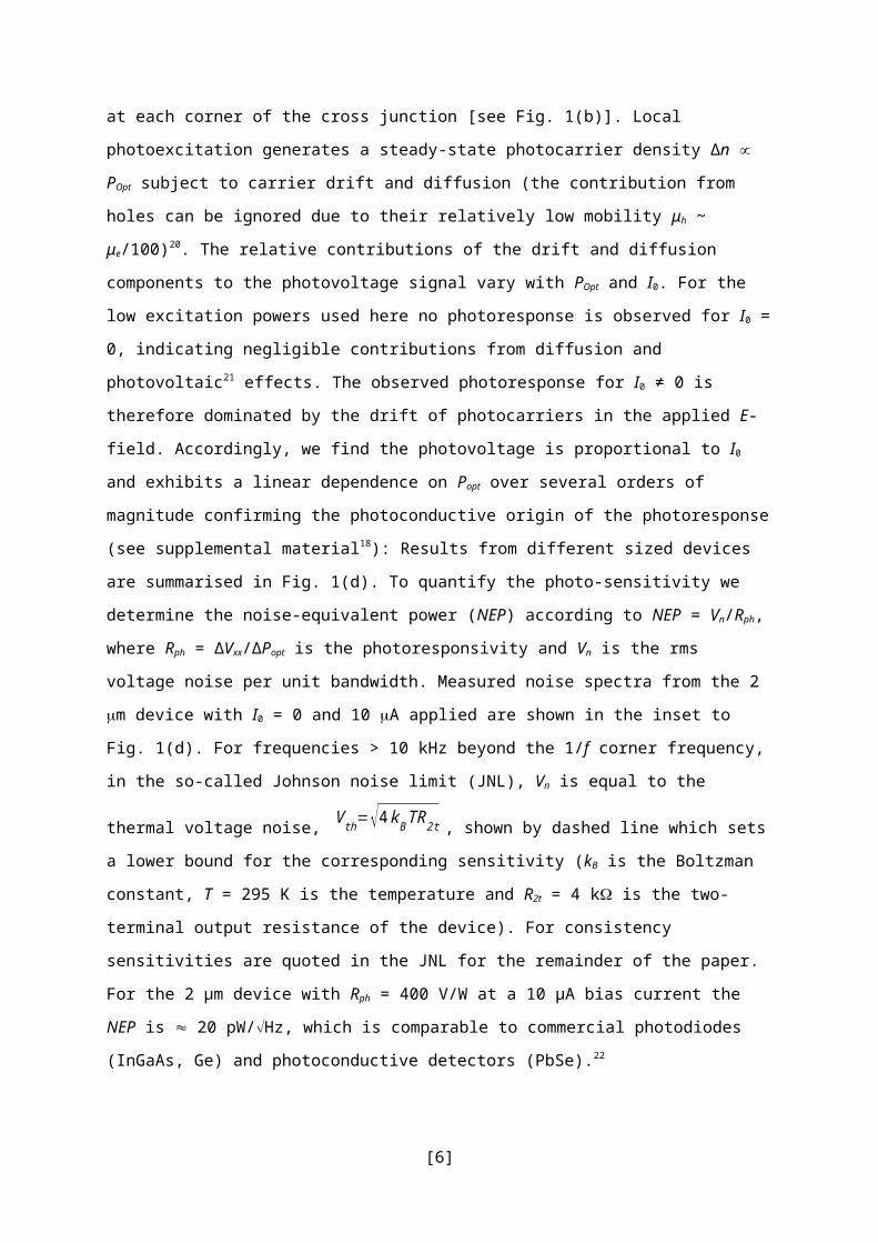
quantify the photo-sensitivity we determine the noise-equivalent power (NEP) according to NEP =
Vn/Rph, where Rph = ΔVxx/ΔPopt is the photoresponsivity and Vn is the rms voltage noise per unit
[3]

bandwidth. Measured noise spectra from the 2 m device with I0 = 0 and 10 A applied are shown in
the inset to Fig. 1(d). For frequencies > 10 kHz beyond the 1/f corner frequency, in the so-called
Johnson noise limit (JNL), Vn is equal to the thermal voltage noise, V th=√4 kB TR2 t , shown by
dashed line which sets a lower bound for the corresponding sensitivity (kB is the Boltzman constant, T
= 295 K is the temperature and R2t = 4 k is the two-terminal output resistance of the device). For
consistency sensitivities are quoted in the JNL for the remainder of the paper. For the 2 μm device
with Rph = 400 V/W at a 10 μA bias current the NEP is 20 pW/Hz, which is comparable to
commercial photodiodes (InGaAs, Ge) and photoconductive detectors (PbSe).22
Additional measurements were performed on a 40 μm wide Hall-bar with Popt = 4 μW, as
shown schematically in Fig. 2(a). This larger sample represents an ‘open’ system in which the mesa
boundaries and adjacent voltage leads are well separated, allowing us to examine the photoresponse
near an individual voltage lead. Fig. 2(b) shows the ΔVxx(x,y) image obtained in the vicinity of voltage
lead A. The photoresponse is characterised by two signal lobes of opposite polarity emanating from
the voltage lead entrance. The corresponding photovoltage map of lead B is reversed due to the
differential (A-B) measurement [see Fig. 2(a)]. To interpret these results we note that close to the
voltage lead entrance, the transverse current density Jx is non-zero and changes direction, as shown by
the sketched current lines in Fig. 2(c). Photocarriers generated above (below) the voltage lead [blue
(red) dot in Fig. 2(c)] undergo net drift towards (away from) the lead thereby causing its potential to
adjust in order to satisfy Jx = 0 in the lead. With knowledge of the photoresponse of an individual
voltage lead, construction of both the ΔVxx(x,y) and ΔVxy(x,y) patterns observed in the ‘closed’ Hall
cross geometry is straightforward by considering the location of the second voltage lead and the
relative current direction. The SPVM images therefore reveal important information about the local E-
field distribution in the device.
Next we discuss the response of the device to local E-fields generated from an electrically
biased metallic SPM-AFM tip (see experimental section). Figs. 3(a) and (b) show electrical SGM
images of the ΔVxx(x,y) and ΔVxy(x,y) voltage outputs from the 2 μm device, obtained with VTip = 3.5
V (rms). It is immediately evident that the general features observed in the SPVM images are
reproduced in the SGM images. Similar results are found for the 1 m and 4 m devices.18 The SGM
images are similar to those reported previously3,23 and can be understood by considering the effect of
the local tip-induced potential well/barrier on the current flow near the voltage leads in a similar way
to the discussion of the SPVM images. Here the charged tip alters the electron density Δn beneath the
tip via capacitive coupling to the 2DEG. Because the conductivity modulation Δ = Δneμ is in-phase
with the AC tip voltage, Δ > 0 as for the photoconductive response. After taking into account the
fraction (2r2/w2) of charge carriers interacting with the tip, it is straightforward to show that
Δσ=μ CV Tip /w2
, where C is the tip-2DEG capacitance. The inset to Fig. 4 shows the linear
[4]

dependence of ΔVxx on VTip from different sized devices, obtained from the centre of the cross. To
accurately determine the sensitivity of the device to electric charge induced on the tip, QTip = CVTip,
calculation of the electrostatic potential around the metallic tip is required which is beyond the scope
of this work. For simplicity, we model the tip as a sphere of radius r = 30 nm separated from the
2DEG by (h + t), where t is the Al0.2In0.8Sb cap thickness. The tip-2DEG capacitance is then given by
C = 2πε0rr2/(hεr + t), where 0 is the permittivity of free space and r ≈ 16 is the relative permittivity
of Al0.2In0.8Sb (estimated using Vegard’s rule for the ternary system24,25 with r(x) ≈ 16.8 – 5.6x). Due
to the small tip radius, coupling to the 2DEG is rather weak, yielding C ≈ 2 aF. To test the validity of
this model we can estimate ΔVxx when the tip is in the cross centre through the relation ΔVxx = I0ΔR,
where ΔR≃− L
wρ0
2 Δσ: For a 2 μm device with w ≈ L, VTip = 3.5V and I0 = 10 μA this simple model
for the tip-2DEG interaction yields ΔVxx ≈ –10 μV, which is in good agreement with the experimental
data. Proceeding with the analysis, we deduce a charge responsivity for the 2 m device of RQ =
ΔVxx/ΔQTip ≈ 240 nV/e at a 10 μA bias current and a charge sensitivity of Vth/RQ ≈ 0.05 e/√Hz. This
sensitivity is significantly greater than previous reports of 2DEG Hall cross structures3 and is
comparable to the best reported single-electron transistor sensitivity at RT.26 Sensitivities derived for
the 1 and 4 um devices are given in supporting information.18 To demonstrate the sensitivity to small
E-fields, in Fig. 4 we show the measured changes in ΔVxx caused by small tip voltages corresponding
to QTip << 1e applied in a step-wise manner. We note that the rms voltage noise for the data in Fig. 4 is
25 nV with the effective measurement bandwidth of 0.42 Hz. This corresponds to Vn 35 nV/√Hz
and a charge sensitivity of 0.15 e/√Hz, in line with the expected sensitivity in the JNL. These
results demonstrate that << 1e charge resolution is readily achieved in the current micro-Hall device.
For completeness, in Fig. 3(c) and (d) we show the magnetic SGM images for ΔVxx(x,y) and
ΔVxy(x,y) (tip magnetisation into the page). Here ΔVxy(x, y) represents the local Hall response [Fig.
3(d)], characterised by a rotationally symmetric signal in the centre of the cross, consistent with
previous magnetic SGM experiments on graphene19,27,28 and InAs 2DEG5 Hall probes. ΔVxx(x, y)
represents the local magnetoresistance of the device and displays a distinct asymmetry about the line
bisecting the adjacent current and voltage leads [Fig. 3(c)]. The symmetry of both ΔVxx(x,y) and
ΔVxy(x,y) follow from the direction of the local Lorentz force (J × B) exerted on the 2DEG by the
magnetic tip [see Fig. 3(c) and (d)]. Using the measured Hall coefficient RH = 1/n0e = 1.25 k/T, we
deduce a magnetic sensitivity of Vth/I0RH ≈ 500 nT/√Hz at 10 μA. This sensitivity greatly exceeds that
of chemical vapour deposited29 and epitaxial30 graphene Hall probes and is comparable to previous
Sb-based 2DEG31 Hall probes with comparable dimensions and bias current.
To model the spatial response of the micro-Hall device to a local non-magnetic conductance perturbation, we consider the four-probe tight-binding
[5]
lattice shown in Fig. 5(a) consisting of 4 crystalline leads labelled 1, 2, 3 and 4 (white regions) connected to a square scattering region (light grey and blue region) to which we introduce disorder. The Hamiltonian matrix elements Hij are
chosen to be –γ for i,j nearest neighbours and onsite energies Hii are chosen to be zero in the leads.
Electrons travelling from one lead to another can possess energies between –4γ and 4γ, where –4γ corresponds to the conduction band edge. Within the
scattering region diagonal elements are chosen to be H ii=εi+ f (ri−r ) , where εi is the onsite energy in site i. To simulate a diffusive scatterer, i is a random number uniformly
distributed over the interval [–W, W] γ. In the simulation, the width of disorder W is chosen to be 0.8 and the average conductance is obtained by averaging over an ensemble of 100 samples. For such disorder with the chosen sample size of 82×82 lattice sites, the system exhibits Ohmic behaviour, where the conductivity is approximately independent of length. For this choice of parameters, the mean free path of the electrons is ≈ 40a obtained by the method described in Ref. 32.To
simulate a local conductance perturbation we introduce a local electrostatic
potential inhomogeneity centred on site i, f (ri−r ) with a Gaussian distribution of radius 5a (a is the lattice constant) and maximum value of –γ. The four-probe resistance is calculated using Landauer-Büttiker formalism33 as the position of the potential inhomogeneity is varied. Using the numbering convention shown in Fig.
5(a), the transverse and longitudinal resistances are Rxy=A32−1−A34
−1 and
Rxx=A42−1−A43
−1, where Aij = Niδij – Tij and i, j ∈ [1, 2, 3]. Ni is the number of open
conduction channels in lead i and Tij is the transmission coefficient between lead i and j calculated using Gollum quantum transport method34 as described in Ref. 35,36.
Figures 5(b) and (c) show the calculated ΔRxx(x,y) = Rxx(x,y) – Rxx0 and ΔRxy(x,y) = Rxy(x,y) – Rxy0 maps for the diffusive regime at a Fermi energy EF = –2γ = –2, where Rxx0 and Rxy0 are the resistances without the potential inhomogeneity. Here EF is chosen to be sufficiently small to ensure an approximately circular Fermi surface. The band structure is then approximately E=−4 γ+γ (k x
2+k y2 ) /2 . This yields a Fermi wavelength of λF ≈ πa. As evidenced by
comparing Fig. 5 with Figs. 1 and 3, the numerical calculations reproduce well the salient features observed in the experimental SPVM and electrical SGM data, validating our approach and interpretation.
[6]

In summary, the real-space voltage response of InSb 2DEG micro-Hall devices to local photo-excitation, electric and magnetic fields have been studied at room temperature using scanning probe techniques. Local photoexcitation is demonstrated to have an analogous effect on the electric field distribution in the 2DEG to that of a local electrostatic gate. In addition to exhibiting high magnetic field
sensitivity, we demonstrate that micro-Hall devices exhibit a photo-sensitivity comparable to
commercial photoconductive sensors and a remarkable sub 1e charge resolution, equal to the best
single electron transistor reports at room temperature.
ACKNOWLEDGEMENTSThe authors gratefully acknowledge funding from the EPSRC (EP/J014699/1). S.A.S. is has also been supported by the NSF (ECCS-0725538), and is a co-founder of PixelEXX, a start-up company whose mission is to market imaging arrays.
[7]

Fig. 1. SPVM images of ΔVxx and ΔVxy from a 2 μm InSb 2DEG micro-Hall device. The outline of the device is
shown by the black lines (I0 = 10 A; Popt = 20 nW). (c) Optical reflection images showing the measurement
configurations (d) Dependence of |ΔVxx|/I0 on Popt for different sized devices, obtained from the centre of the
cross. Inset shows voltage noise spectra from the 2 μm device.
Fig. 2. (a) Schematic of the macroscopic Hall-bar and measurement geometry; The dashed box indicates the
scanned area; Coloured lobes represent the observed photovoltage signals. (b) SPVM image of ΔVxx in the
vicinity of a voltage lead A (I0 = 100 A; Popt = 4 μW). (c) Optical reflection image with a sketch of the current
lines near the voltage lead.
[8]

Fig. 3. (a,b) Electrical SGM images of ΔVxx and ΔVxy from the 2 μm device (VTip = 3.53 V, I0 = 10 A). (c,d)
Magnetic SGM images of ΔVxx and ΔVxy (tip magnetisation into the page); the current flow and direction of
Lorentz force are shown schematically by the black and white arrows, respectively.
Fig. 4. Changes in ΔVxx from the 2 μm device caused by small voltages applied to the tip in a step-wise manner
(25 mV increments). Inset shows the linear dependence of ΔVxx on VTip for different sized devices, obtained from
the centre of the cross. (I0 = 10 A, fTip = 2.5 kHz).
[9]

Fig. 5. (a) Schematic diagram of the calculated structure. Calculated (b) ΔRxx and (c) ΔRxy maps in the 82×82 site
scattering region.
[10]

Reference List
1. Boero, G.; Demierre, M.; Besse, P. A.; Popovic, R. S. Micro-Hall devices: performance, technologies and applications. Sensors and Actuators A-Physical 2003, 106 (1-3), 314-320.
2. Lenz, J.; Edelstein, A. S. Magnetic sensors and their applications. Ieee Sensors Journal 2006, 6 (3), 631-649.
3. Barbolina, I. I.; Novoselov, K. S.; Morozov, S. V.; Dubonos, S. V.; Missous, M.; Volkov, A. O.; Christian, D. A.; Grigorieva, I. V.; Geim, A. K. Submicron sensors of local electric field with single-electron resolution at room temperature. Applied Physics Letters 2006, 88 (1), 013901.
4. Baumgartner, A.; Ihn, T.; Ensslin, K.; Papp, G.; Peeters, F.; Maranowski, K.; Gossard, A. C. Classical Hall effect in scanning gate experiments. Physical Review B 2006, 74 (16), 165426.
5. Folks, L.; Troup, A. S.; Boone, T. D.; Katine, J. A.; Nishioka, M.; Grobis, M.; Sullivan, G. J.; Ikhlassi, A.; Field, M.; Gurney, B. A. Near-surface nanoscale InAs Hall cross sensitivity to localized magnetic and electric fields. Journal of Physics-Condensed Matter 2009, 21 (25), 255802.
6. Topinka, M. A.; Leroy, B. J.; Westervelt, R. M.; Maranowski, K. D.; Gossard, A. C. Imaging coherent electron wave flow in a two-dimensional electron gas. Physica E-Low-Dimensional Systems & Nanostructures 2002, 12 (1-4), 678-683.
7. Aidala, K. E.; Parrott, R. E.; Kramer, T.; Heller, E. J.; Westervelt, R. M.; Hanson, M. P.; Gossard, A. C. Imaging magnetic focusing of coherent electron waves. Nature Physics 2007, 3 (7), 464-468.
8. Shashkin, A. A.; Kent, A. J.; Owers-Bradley, J. R.; Cross, A. J.; Hawker, P.; Henini, M. Hall photovoltage imaging of the edge of a quantum Hall device. Physical Review Letters 1997, 79 (25), 5114-5117.
9. vanHaren, R. J. F.; deLange, W.; Blom, F. A. P.; Wolter, J. H. Imaging of Edge Channels in the Integer Quantum Hall Regime by the Lateral Photoelectric Effect. Physical Review B 1995, 52 (8), 5760-5766.
10. Hof, K. D.; Kaiser, F. J.; Stallhofer, M.; Schuh, D.; Wegscheider, W.; Hanggi, P.; Kohler, S.; Kotthaus, J. P.; Holleitner, A. W. Spatially Resolved Ballistic Optoelectronic Transport Measured by Quantized Photocurrent Spectroscopy. Nano Letters 2010, 10 (10), 3836-3840.
11. Nadvornik, L.; Haigh, J. A.; Olejnik, K.; Irvine, A. C.; Novak, V.; Jungwirth, T.; Wunderlich, J. Efficient conversion of light to charge and spin in Hall-bar microdevices. Physical Review B 2015, 91 (12), 125205.
[11]

12. Newaz, A. K. M.; Chang, W. J.; Wallace, K. D.; Edge, L. C.; Wickline, S. A.; Bashir, R.; Gilbertson, A. M.; Cohen, L. F.; Solin, S. A. A nanoscale Ti/GaAs metal-semiconductor hybrid sensor for room temperature light detection. Applied Physics Letters 2010, 97 (8), 082105.
13. Tran, L. C.; Werner, F. M.; Newaz, A. K. M.; Solin, S. A. Photo effects at the Schottky interface in extraordinary optoconductance. Journal of Applied Physics 2013, 114 (15), 153110.
14. Orr, J. M. S.; Gilbertson, A. M.; Fearn, M.; Croad, O. W.; Storey, C. J.; Buckle, L.; Emeny, M. T.; Buckle, P. D.; Ashley, T. Electronic transport in modulation-doped InSb quantum well heterostructures. Physical Review B 2008, 77 (16), 165334.
15. Gilbertson, A. M.; Kormanyos, A.; Buckle, P. D.; Fearn, M.; Ashley, T.; Lambert, C. J.; Solin, S. A.; Cohen, L. F. Room temperature ballistic transport in InSb quantum well nanodevices. Applied Physics Letters 2011, 99 (24).
16. Wang, L.; Meric, I.; Huang, P. Y.; Gao, Q.; Gao, Y.; Tran, H.; Taniguchi, T.; Watanabe, K.; Campos, L. M.; Muller, D. A.; Guo, J.; Kim, P.; Hone, J.; Shepard, K. L.; Dean, C. R. One-Dimensional Electrical Contact to a Two-Dimensional Material. Science 2013, 342 (6158), 614-617.
17. Gilbertson, A. M.; Buckle, P. D.; Emeny, M. T.; Ashley, T.; Cohen, L. F. Suppression of the parasitic buffer layer conductance in InSb/AlxIn1-xSb heterostructures using a wide-band-gap barrier layer. Physical Review B 2011, 84 (7), 075474.
18. See supplemental material at [URL inserted by AIP] for additional information and data from devices. See supplemental material at [URL inserted by AIP] for additional information and data from devices.
19. Panchal, V.; Iglesias-Freire, O.; Lartsev, A.; Yakimova, R.; Asenjo, A.; Kazakova, O. Magnetic Scanning Probe Calibration Using Graphene Hall Sensor. Ieee Transactions on Magnetics 2013, 49 (7), 3520-3523.
20. Gu, P.; Tani, M.; Kono, S.; Sakai, K.; Zhang, X. C. Study of terahertz radiation from InAs and InSb. Journal of Applied Physics 2002, 91 (9), 5533-5537.
21. Tabatabaie, N.; Meynadier, M. H.; Nahory, R. E.; Harbison, J. P.; Florez, L. T. Large Lateral Photovoltaic Effect in Modulation-Doped Algaas/Gaas Heterostructures. Applied Physics Letters 1989, 55 (8), 792-794.
22. Thorlabs.de. IR Photoconductive Detectors [Online]. http://www.thorlabs.de/newgrouppage9.cfm?objectgroup_id=6479 [29 Jun. 2015]. 2015.
Ref Type: Online Source
23. Papp, G.; Peeters, F. M. Resistance maps for a submicron Hall electrosensor in the diffusive regime. Journal of Applied Physics 2007, 101 (11), 113717.
24. Dixon, J. R.; Furdyna, J. K. Measurement of the Static Dielectric-Constant of the Insb Lattice Via Gyrotropic Sphere Resonances. Solid State Communications 1980, 35 (2), 195-198.
[12]

25. Zollner, S.; Lin, C. T.; Schonherr, E.; Bohringer, A.; Cardona, M. The Dielectric Function of Alsb from 1.4-Ev to 5.8-Ev Determined by Spectroscopic Ellipsometry. Journal of Applied Physics 1989, 66 (1), 383-387.
26. Pashkin, Y. A.; Nakamura, Y.; Tsai, J. S. Room-temperature Al single-electron transistor made by electron-beam lithography. Applied Physics Letters 2000, 76 (16), 2256-2258.
27. Rajkumar, R. K.; Manzin, A.; Cox, D. C.; Silva, S. R. P.; Tzalenchuk, A.; Kazakova, O. 3-D Mapping of Sensitivity of Graphene Hall Devices to Local Magnetic and Electrical Fields. Ieee Transactions on Magnetics 2013, 49 (7), 3445-3448.
28. Rajkumar, R. K.; Asenjo, A.; Panchal, V.; Manzin, A.; Iglesias-Freire, O.; Kazakova, O. Magnetic scanning gate microscopy of graphene Hall devices (invited). Journal of Applied Physics 2014, 115 (17), 172606.
29. Tang, C. C.; Li, M. Y.; Li, L. J.; Chi, C. C.; Chen, J. C. Characteristics of a sensitive micro-Hall probe fabricated on chemical vapor deposited graphene over the temperature range from liquid-helium to room temperature. Applied Physics Letters 2011, 99 (11), 122107.
30. Panchal, V.; Cedergren, K.; Yakimova, R.; Tzalenchuk, A.; Kubatkin, S.; Kazakova, O. Small epitaxial graphene devices for magnetosensing applications. Journal of Applied Physics 2012, 111 (7), 07E509.
31. Bando, M.; Ohashi, T.; Dede, M.; Akram, R.; Oral, A.; Park, S. Y.; Shibasaki, I.; Handa, H.; Sandhu, A. High sensitivity and multifunctional micro-Hall sensors fabricated using InAlSb/InAsSb/InAlSb heterostructures. Journal of Applied Physics 2009, 105 (7), 07E909.
32. Ferrer, J.; Lambert, C. J.; Garcia-Suarez, V. M.; Manrique, D. Z.; Visontai, D.; Oroszlany, L.; Rodriguez-Ferradas, R.; Grace, I.; Bailey, S. W. D.; Gillemot, K.; Sadeghi, H.; Algharagholy, L. A. GOLLUM: a next-generation simulation tool for electron, thermal and spin transport. New Journal of Physics 2014, 16, 093029.
33. Buttiker, M. 4-Terminal Phase-Coherent Conductance. Physical Review Letters 1986, 57 (14), 1761-1764.
34. Ferrer, J.; Lambert, C. J.; Garcia-Suarez, V. M.; Manrique, D. Z.; Visontai, D.; Oroszlany, L.; Rodriguez-Ferradas, R.; Grace, I.; Bailey, S. W. D.; Gillemot, K.; Sadeghi, H.; Algharagholy, L. A. GOLLUM: a next-generation simulation tool for electron, thermal and spin transport. New Journal of Physics 2014, 16.
35. Sadeghi, H.; Sangtarash, S.; Lambert, C. J. Enhancing the thermoelectric figure of merit in engineered graphene nanoribbons. Beilstein Journal of Nanotechnology 2015, 6, 1176-1182.
36. Sadeghi, H.; Mol, J. A.; Lau, C. S.; Briggs, G. A. D.; Warner, J.; Lambert, C. J. Conductance enlargement in picoscale electroburnt graphene nanojunctions. Proceedings of the National Academy of Sciences of the United States of America 2015, 112 (9), 2658-2663.
[13]

[14]