Version 1 - Envoy Data Memoryenvoydatamemory.com/datasheets/EN-L0J Industrial... · microSD 3.0...
22
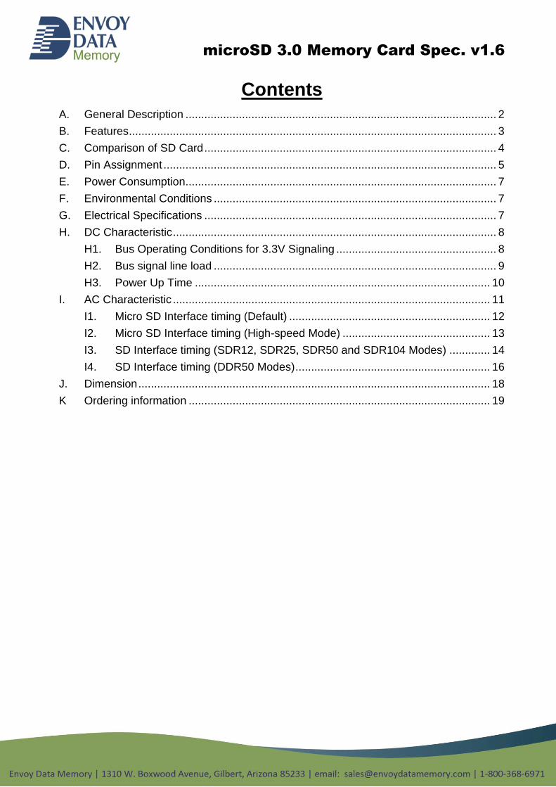
microSD 3.0 Memory Card Specification Version 1.6
Transcript of Version 1 - Envoy Data Memoryenvoydatamemory.com/datasheets/EN-L0J Industrial... · microSD 3.0...

microSD 3.0 Memory Card
Specification
Version 1.6
microSD 3.0 Memory Card Spec. v1.6
Contents
A. General Description ................................................................................................... 2
B. Features ..................................................................................................................... 3
C. Comparison of SD Card ............................................................................................. 4
D. Pin Assignment .......................................................................................................... 5
E. Power Consumption ................................................................................................... 7
F. Environmental Conditions .......................................................................................... 7
G. Electrical Specifications ............................................................................................. 7
H. DC Characteristic ....................................................................................................... 8
H1. Bus Operating Conditions for 3.3V Signaling ................................................... 8
H2. Bus signal line load .......................................................................................... 9
H3. Power Up Time .............................................................................................. 10
I. AC Characteristic ..................................................................................................... 11
I1. Micro SD Interface timing (Default) ................................................................ 12
I2. Micro SD Interface timing (High-speed Mode) ............................................... 13
I3. SD Interface timing (SDR12, SDR25, SDR50 and SDR104 Modes) ............. 14
I4. SD Interface timing (DDR50 Modes) .............................................................. 16
J. Dimension ................................................................................................................ 18
K Ordering information ................................................................................................ 19
microSD 3.0 Memory Card Spec. v1.6
A. General Description
The Secure Digital (SD) card version 3.0 is fully compliant to the specification
released by SD Card Association. The Command List supports [Part 1 Physical Layer
Specification Ver3.01 Final] definitions. Card Capacity of Non-secure Area, Secure
Area Supports [Part 3 Security Specification Ver3.0 Final] Specifications.
The SD 3.0 card is based on 9-pin interface, designed to operate at a maximum
operating frequency of 208MHz. It can alternate communication protocol between the
SD mode and SPI mode. It performs data error detection and correction with very low
power consumption. The Card capacity could be more than 64GB and up to 2TB with
ex-FAT which is called SDXC (Extended Capacity SD Memory Card).
Secure Digital 3.0 card is one of the most popular cards today based on its high
performance, good reliability and wide compatibility.

microSD 3.0 Memory Card Spec. v1.6
B. Features
Support SD system specification version 3.0
Card Capacity of Non-secure Area, Secure Area Supports [Part 3 Security
Specification Ver3.0 Final] Specifications
Capacity of SD3.0 Memory
- SDSC: Up to and including 2 GB
- SDHC: More than 2GB and up to and including 32GB
- SDXC: More than 32GB and up to and including 2TB
Support SD SPI mode
Designed for read-only and read/write cards.
Bus Speed Mode (using 4 parallel data lines)
- Default Speed mode: 3.3V signaling, Frequency up to 25 MHz, up to 12.5 MB/sec
- High Speed mode: 3.3V signaling, Frequency up to 50 MHz, up to 25 MB/sec
- SDR12 - SDR up to 25MHz 1.8V signaling
- SDR25 - SDR up to 50MHz 1.8V signaling
- SDR50: 1.8V signaling, Frequency up to 100 MHz, up to 50MB/sec
- SDR104: 1.8V signaling, Frequency up to 208MHz, up to 104MB/sec
- DDR50: 1.8V signaling, Frequency up to 50 MHz, sampled on both clock edges, up
to 50MB/sec
Note: Timing in 1.8V signaling is different from that of 3.3V signaling.
The Command List supports [Part 1 Physical Layer Specification Ver3.1 Final]
definitions
Copyrights Protection Mechanism - Complies with highest security of CPRM
standard
CPRM (Content Protection for Recordable Media) of SD Card supported.
Card removal during read operation will never harm the content
Password Protection of cards (option)
Write Protect feature using mechanical switch

microSD 3.0 Memory Card Spec. v1.6
Built-in write protection features (permanent and temporary)
+4KV/-4KV ESD protection in contact pads.
Dimension : 15mm(L) x 11mm(W) x 1mm(H)
Operating voltage range : 2.7-3.6 V
Supported two types of wear-leveling: Dynamic and Static Wear-Leveling.
C. Comparison of SD Card
SD3.0 Standard
(Backward compatible to
2.0 host)
SD3.0 SDHC
(Backward compatible to
2.0 host)
SD3.0 SDXC
Addressing Mode Byte
(1 byte unit)
Block
(512 byte unit)
Block
(512 byte unit)
HCS/CCS bits of ACMD41 Support Support Support
CMD8 (SEND_IF_COND) Support Support Support
CMD16 (SET_BLOCKLEN) Support Support
(Only CMD42)
Support
(Only CMD42)
Partial Read Support Not Support Not Support
Lock/Unlock Function Mandatory Mandatory Mandatory
Write Protect Groups Optional Not Support Not Support
Supply Voltage 2.0v – 2.7v
(for initialization) Not Support Not Support Not Support
Total Bus Capacitance for each signal line
40pF 40pF 40pF
CSD Version
(CSD_STRUCTURE Value) 1.0 (0x0) 2.0 (0x1) 2.0 (0x1)
Speed Class Optional
Mandatory
(Class 2 / 4 / 6 / 10)
Mandatory
(Class 2 / 4 / 6 / 10)

microSD 3.0 Memory Card Spec. v1.6
D. Pin Assignment
Micro SD memory Card Pin Assignment
pin SD Mode SPI Mode
Name Type1 Description Name Type Description
1 DAT2 I/O/PP Data Line[bit2] RSV
2 CD/DAT3 2 I/O/PP 3 Card Detect/
Data Line[bit3] CS I 3 Chip Select (neg true)
3 CMD PP Command/Response DI I Data In
4 VDD S Supply voltage VDD S Supply voltage
5 CLK I Clock SCLK I Clock
6 VSS S Supply voltage
ground VSS S Supply voltage ground
7 DAT0 I/O/PP Data Line[bit0] DO O/PP Data Out
8 DAT1 I/O/PP Data Line[bit1] RSV
(1) S: power supply, I:input; O:output using push-pull drivers; PP:I/O using push-pull drivers.
(2) The extended DAT lines(DAT1-DAT3)are input on power up. They start to operate as DAT
lines after SET_BUS_WIDTH command. The Host shall keep its own DAT1-DAT3 lines in input
mode, as well, while they are not used. It is defined so, in order to keep compatibility to Multi-Media
Cards.
(3) At power up this line has a 50KOhm pull up enabled in the card. This resistor serves two
functions Card detection and Mode Selection. For Mode Selection, the host can drive the line
high or let it be pulled high to select SD mode. If the host wants to select SPI mode it should
drive the line low. For Card detection, the host detects that the line is pulled high. This pull-up
should be disconnected by the user, during regular data transfer, with
SET_CLR_CARD_DETECT(ACMD42) command.

microSD 3.0 Memory Card Spec. v1.6
Name Width Description
CID 128bit Card identification number; card individual number for
identification. Mandatory
RCA1 16bit
Relative card address; local system address of a card, dynamically
suggested by the card and approved by the host during
initialization. Mandatory
DSR 16bit Driver Stage Register; to configure the card’s output drivers.
Optional
CSD 128bit Card Specific Data; information about the card operation
conditions. Mandatory
SCR 64bit SD Configuration Register; information about the SD Memory
Card's Special Features capabilities Mandatory
OCR 32bit Operation conditions register. Mandatory.
SSR 512bit SD Status; information about the card proprietary features
Mandatory
OCR 32bit Card Status; information about the card status
Mandatory
(1) RCA register is not used (available) in SPI mode

microSD 3.0 Memory Card Spec. v1.6
E. Power Consumption
Table list as below is the power consumption of SD card with different type of flash memory. (PS8035 + Flash Memory)
Flash mode Max Power up
Current (uA)
Max Stand by
Current (uA)
Max Read
Current (mA)
Max Write
Current (mA)
Single(1)
flash(1x8bit) 150 150 100@ 3.6V 100@ 3.6V
SDR/DDR 250 250 [email protected] [email protected]
(1)Data transfer mode is single channel.
F. Environmental Conditions
Temperature: -25 to 85in storage/ Operating: 0to 70 “C” Temp & -40C to 85C “I” Temp.
Humidity: RH=93% under 25 in operating/ RH=93% under 40 in non-operating.
Drop Test: 1.5m free fall.
Torque Test: 0.15N-m or +/-2.5deg.
G. Electrical Specifications
Absolute Maximum Rating
Item Symbol Parameter MIN MAX Unit
1 VDD-VSS DC Power Supply -0.3 +3.3 V
2 VIN Input Voltage VSS-0.3 VDD+0.3 V
3 Ta Operating Temperature 0 +70 V
4 Tst Storage Temperature -25 +85 V
Parameter Symbol Min MAX Unit
Operating Temperature Ta 0 +70 V
VDD Voltage VDD 2.7 3.6 V
microSD 3.0 Memory Card Spec. v1.6
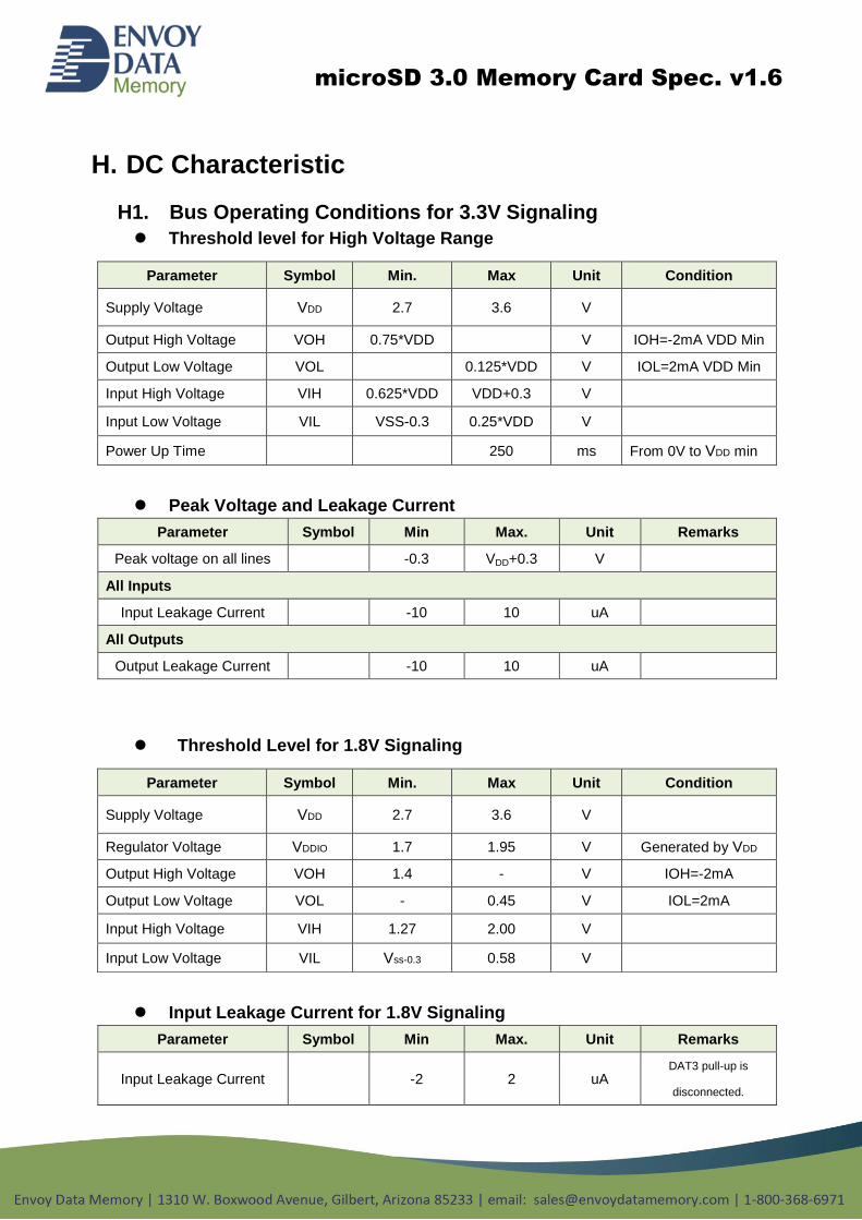
H. DC Characteristic
H1. Bus Operating Conditions for 3.3V Signaling
Threshold level for High Voltage Range
Peak Voltage and Leakage Current
Parameter Symbol Min Max. Unit Remarks
Peak voltage on all lines -0.3 VDD+0.3 V
All Inputs
Input Leakage Current -10 10 uA
All Outputs
Output Leakage Current -10 10 uA
Threshold Level for 1.8V Signaling
Input Leakage Current for 1.8V Signaling
Parameter Symbol Min Max. Unit Remarks
Input Leakage Current -2 2 uA DAT3 pull-up is
disconnected.
Parameter Symbol Min. Max Unit Condition
Supply Voltage VDD 2.7 3.6 V
Output High Voltage VOH 0.75*VDD V IOH=-2mA VDD Min
Output Low Voltage VOL 0.125*VDD V IOL=2mA VDD Min
Input High Voltage VIH 0.625*VDD VDD+0.3 V
Input Low Voltage VIL VSS-0.3 0.25*VDD V
Power Up Time 250 ms From 0V to VDD min
Parameter Symbol Min. Max Unit Condition
Supply Voltage VDD 2.7 3.6 V
Regulator Voltage VDDIO 1.7 1.95 V Generated by VDD
Output High Voltage VOH 1.4 - V IOH=-2mA
Output Low Voltage VOL - 0.45 V IOL=2mA
Input High Voltage VIH 1.27 2.00 V
Input Low Voltage VIL Vss-0.3 0.58 V
microSD 3.0 Memory Card Spec. v1.6
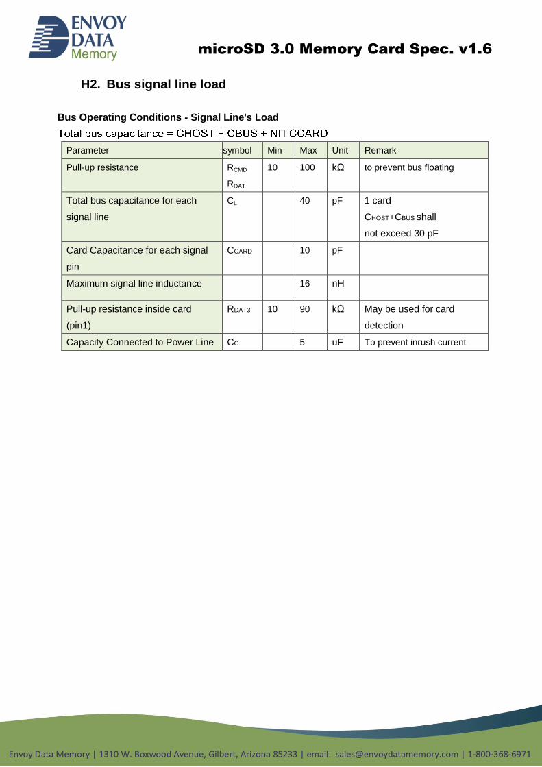
H2. Bus signal line load
Bus Operating Conditions - Signal Line's Load
Parameter symbol Min Max Unit Remark
Pull-up resistance RCMD
RDAT
10 100 kΩ to prevent bus floating
Total bus capacitance for each
signal line
CL 40 pF 1 card
CHOST+CBUS shall
not exceed 30 pF
Card Capacitance for each signal
pin
CCARD 10 pF
Maximum signal line inductance 16 nH
Pull-up resistance inside card
(pin1)
RDAT3
10 90 kΩ May be used for card
detection
Capacity Connected to Power Line CC 5 uF To prevent inrush current
microSD 3.0 Memory Card Spec. v1.6
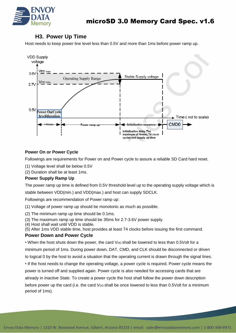
H3. Power Up Time
Host needs to keep power line level less than 0.5V and more than 1ms before power ramp up.
Power On or Power Cycle
Followings are requirements for Power on and Power cycle to assure a reliable SD Card hard reset.
(1) Voltage level shall be below 0.5V
(2) Duration shall be at least 1ms. Power Supply Ramp Up
The power ramp up time is defined from 0.5V threshold level up to the operating supply voltage which is
stable between VDD(min.) and VDD(max.) and host can supply SDCLK.
Followings are recommendation of Power ramp up:
(1) Voltage of power ramp up should be monotonic as much as possible.
(2) The minimum ramp up time should be 0.1ms.
(3) The maximum ramp up time should be 35ms for 2.7-3.6V power supply. (4) Host shall wait until VDD is stable. (5) After 1ms VDD stable time, host provides at least 74 clocks before issuing the first command. Power Down and Power Cycle
• When the host shuts down the power, the card VDD shall be lowered to less than 0.5Volt for a
minimum period of 1ms. During power down, DAT, CMD, and CLK should be disconnected or driven
to logical 0 by the host to avoid a situation that the operating current is drawn through the signal lines.
• If the host needs to change the operating voltage, a power cycle is required. Power cycle means the
power is turned off and supplied again. Power cycle is also needed for accessing cards that are
already in Inactive State. To create a power cycle the host shall follow the power down description
before power up the card (i.e. the card VDD shall be once lowered to less than 0.5Volt for a minimum
period of 1ms).

microSD 3.0 Memory Card Spec. v1.6
I. AC Characteristic

microSD 3.0 Memory Card Spec. v1.6
I1. Micro SD Interface timing (Default)
Parameter Symbol Min Max Unit Remark
Clock CLK (All values are referred to min(VIH) and max(VIL)
Clock frequency Data Transfer Mode
fPP
0 25 MHz Ccard≤ 10 pF
(1 card)
Clock frequency Identification Mode
fOD 0(1)/100 400 kHz Ccard≤ 10 pF
(1 card)
Clock low time tWL 10 ns Ccard≤ 10 pF
(1 card)
Clock high time tWH 10 ns Ccard≤ 10 pF
(1 card)
Clock rise time tTLH 10 ns Ccard≤ 10 pF
(1 card)
Clock fall time tTHL 10 ns Ccard≤ 10 pF
(1 card)
Inputs CMD, DAT (referenced to CLK)
Input set-up time tISU 5 ns Ccard≤ 10 pF
(1 card)
Input hold time tIH 5 ns Ccard≤ 10 pF
(1 card)
Outputs CMD, DAT (referenced to CLK)
Output Delay time during Data Transfer Mode
tODLY 0 14 ns CL≤40 pF (1 card)
Output Delay time during Identification Mode
tODLY 0 50 ns CL≤40 pF (1 card)
(1) 0Hz means to stop the clock. The given minimum frequency range is for cases were continues
clock is required.

microSD 3.0 Memory Card Spec. v1.6
I2. Micro SD Interface timing (High-speed Mode)
Parameter Symbol Min Max Unit Remark
Clock CLK (All values are referred to min(VIH) and max(VIL)
Clock frequency Data Transfer Mode
fPP
0 50 MHz Ccard≤10 pF
(1 card)
Clock low time tWL 7 ns Ccard≤10 pF
(1 card)
Clock high time tWH 7 ns Ccard≤10 pF
(1 card)
Clock rise time tTLH 3 ns Ccard≤10 pF
(1 card)
Clock fall time tTHL 3 ns Ccard≤10 pF
(1 card)
Inputs CMD, DAT (referenced to CLK)
Input set-up time tISU 6 ns Ccard≤10 pF
(1 card)
Input hold time tIH 2 ns Ccard≤10 pF
(1 card)
Outputs CMD, DAT (referenced to CLK)
Output Delay time during Data Transfer Mode
tODLY 14 ns CL≤40 pF (1 card)
Output Hold time TOH 2.5 ns CL≤15 pF (1 card)
Total System capacitance of each line¹
CL 40 pF CL≤15 pF (1 card)
(1) In order to satisfy severe timing, host shall drive only one card.
microSD 3.0 Memory Card Spec. v1.6
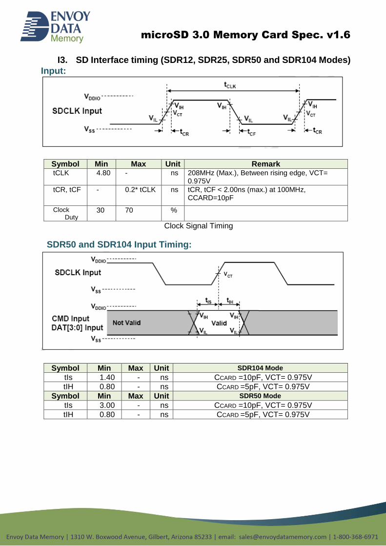
I3. SD Interface timing (SDR12, SDR25, SDR50 and SDR104 Modes)
Input:
Symbol Min Max Unit Remark tCLK 4.80 - ns 208MHz (Max.), Between rising edge, VCT=
0.975V
tCR, tCF - 0.2* tCLK ns tCR, tCF < 2.00ns (max.) at 100MHz, CCARD=10pF
Clock Duty
30 70 %
Clock Signal Timing
SDR50 and SDR104 Input Timing:
Symbol Min Max Unit SDR104 Mode
tIs 1.40 - ns CCARD =10pF, VCT= 0.975V
tIH 0.80 - ns CCARD =5pF, VCT= 0.975V
Symbol Min Max Unit SDR50 Mode
tIs 3.00 - ns CCARD =10pF, VCT= 0.975V
tIH 0.80 - ns CCARD =5pF, VCT= 0.975V

microSD 3.0 Memory Card Spec. v1.6
Output Timing of Fixed Data Window (SDR12, SDR25 and SDR50):
Symbol Min Max Uni
t Remark
tODLY - 7.5 ns tCLK>=10.0ns, CL=30pF, using driver Type B,
for SDR50
tODLY - 14 ns tCLK>=20.0ns, CL=40pF, using driver Type B,
for SDR25 and SDR12,
TOH 1.5 - ns Hold time at the tODLY (min.), CL=15pF
Output Timing of Fixed Data Window
Output Timing of Variable Window (SDR104):
Symbol Min Max Uni
t Remark
tOP 0 2 Ul Card Output Phase
tOP -350 +1550 ps Delay variable due to temperature change
after tuning
tODW 0.60 - Ul tODW=2.88ns at 208MHz

microSD 3.0 Memory Card Spec. v1.6
I4. SD Interface timing (DDR50 Modes)
Symbol Min Max Unit Remark
tCLK 20 - ns 50MHz (Max.), Between rising edge
tCR, tCF - 0.2* tCLK ns tCR, tCF < 4.00ns (max.) at 50MHz, CCARD=10pF
Clock Duty 45 55 %
Clock Signal Timing
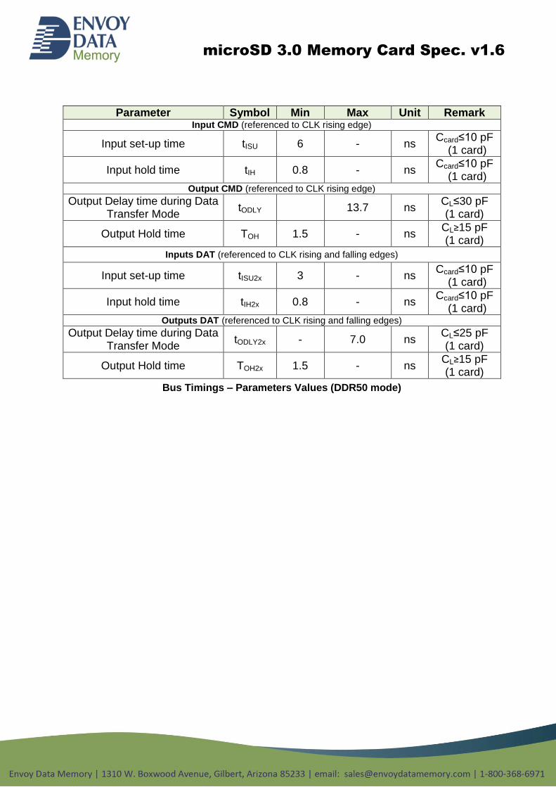
microSD 3.0 Memory Card Spec. v1.6
Parameter Symbol Min Max Unit Remark Input CMD (referenced to CLK rising edge)
Input set-up time tISU 6 - ns Ccard≤10 pF
(1 card)
Input hold time tIH 0.8 - ns Ccard≤10 pF
(1 card) Output CMD (referenced to CLK rising edge)
Output Delay time during Data Transfer Mode
tODLY 13.7 ns CL≤30 pF (1 card)
Output Hold time TOH 1.5 - ns CL≥15 pF (1 card)
Inputs DAT (referenced to CLK rising and falling edges)
Input set-up time tISU2x 3 - ns Ccard≤10 pF
(1 card)
Input hold time tIH2x 0.8 - ns Ccard≤10 pF
(1 card) Outputs DAT (referenced to CLK rising and falling edges)
Output Delay time during Data Transfer Mode
tODLY2x - 7.0 ns CL≤25 pF (1 card)
Output Hold time TOH2x 1.5 - ns CL≥15 pF (1 card)
Bus Timings – Parameters Values (DDR50 mode)
microSD 3.0 Memory Card Spec. v1.6
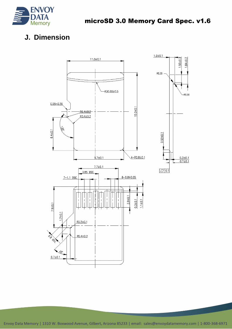
J. Dimension

microSD 3.0 Memory Card Spec. v1.6
K Ordering information
PART NUMBER DESCRIPTION
SLC – C TEMP µSD CARDS
EN-L0J128MDSC 128MB SLC µSD CARD C TEMP
EN-L0J256MDSC 256MB SLC µSD CARD C TEMP
EN-L0J512MDSC 512MB SLC µSD CARD C TEMP
EN-L0J001GDSC 1GB SLC µSD CARD C TEMP
EN-L0J002GDSC 2GB SLC µSD CARD C TEMP
EN-L0J004GDSC 4GB SLC µSD CARD C TEMP
PART NUMBER DESCRIPTION
SLC – I TEMP µSD CARDS
EN-L0J128MDSI 128MB SLC µSD CARD I TEMP
EN-L0J256MDSI 256MB SLC µSD CARD I TEMP
EN-L0J512MDSI 512MB SLC µSD CARD I TEMP
EN-L0J001GDSI 1GB SLC µSD CARD I TEMP
EN-L0J002GDSI 2GB SLC µSD CARD I TEMP
EN-L0J004GDSI 4GB SLC µSD CARD I TEMP
microSD 3.0 Memory Card Spec. v1.6
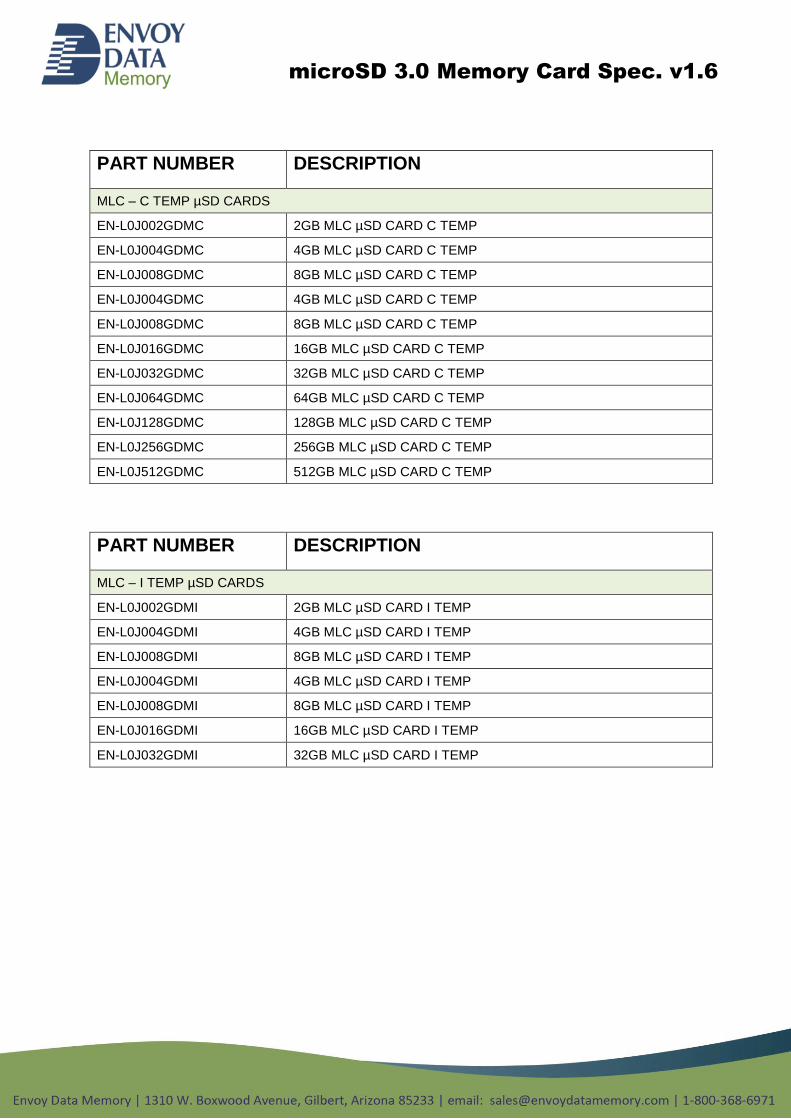
PART NUMBER DESCRIPTION
MLC – C TEMP µSD CARDS
EN-L0J002GDMC 2GB MLC µSD CARD C TEMP
EN-L0J004GDMC 4GB MLC µSD CARD C TEMP
EN-L0J008GDMC 8GB MLC µSD CARD C TEMP
EN-L0J004GDMC 4GB MLC µSD CARD C TEMP
EN-L0J008GDMC 8GB MLC µSD CARD C TEMP
EN-L0J016GDMC 16GB MLC µSD CARD C TEMP
EN-L0J032GDMC 32GB MLC µSD CARD C TEMP
EN-L0J064GDMC 64GB MLC µSD CARD C TEMP
EN-L0J128GDMC 128GB MLC µSD CARD C TEMP
EN-L0J256GDMC 256GB MLC µSD CARD C TEMP
EN-L0J512GDMC 512GB MLC µSD CARD C TEMP
PART NUMBER DESCRIPTION
MLC – I TEMP µSD CARDS
EN-L0J002GDMI 2GB MLC µSD CARD I TEMP
EN-L0J004GDMI 4GB MLC µSD CARD I TEMP
EN-L0J008GDMI 8GB MLC µSD CARD I TEMP
EN-L0J004GDMI 4GB MLC µSD CARD I TEMP
EN-L0J008GDMI 8GB MLC µSD CARD I TEMP
EN-L0J016GDMI 16GB MLC µSD CARD I TEMP
EN-L0J032GDMI 32GB MLC µSD CARD I TEMP
microSD 3.0 Memory Card Spec. v1.6
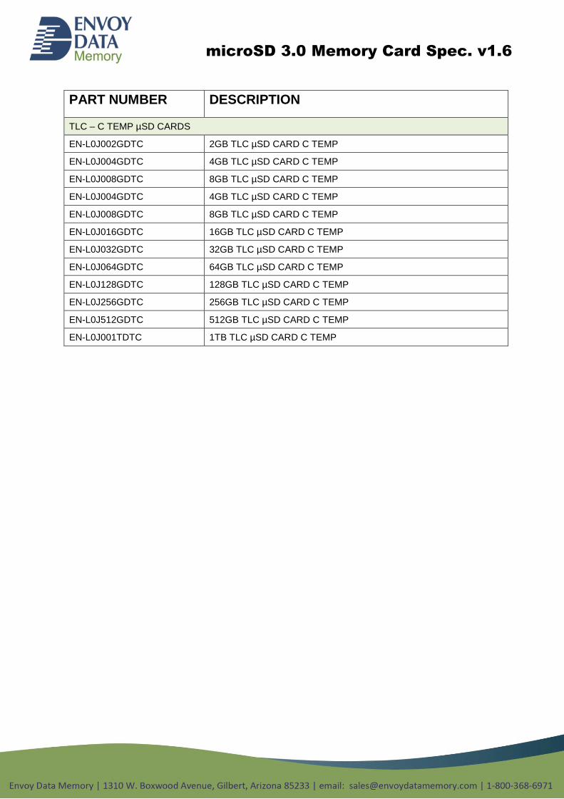
PART NUMBER DESCRIPTION
TLC – C TEMP µSD CARDS
EN-L0J002GDTC 2GB TLC µSD CARD C TEMP
EN-L0J004GDTC 4GB TLC µSD CARD C TEMP
EN-L0J008GDTC 8GB TLC µSD CARD C TEMP
EN-L0J004GDTC 4GB TLC µSD CARD C TEMP
EN-L0J008GDTC 8GB TLC µSD CARD C TEMP
EN-L0J016GDTC 16GB TLC µSD CARD C TEMP
EN-L0J032GDTC 32GB TLC µSD CARD C TEMP
EN-L0J064GDTC 64GB TLC µSD CARD C TEMP
EN-L0J128GDTC 128GB TLC µSD CARD C TEMP
EN-L0J256GDTC 256GB TLC µSD CARD C TEMP
EN-L0J512GDTC 512GB TLC µSD CARD C TEMP
EN-L0J001TDTC 1TB TLC µSD CARD C TEMP