Versatile Z-Axis Interconnection-Based Coreless Technology...
6
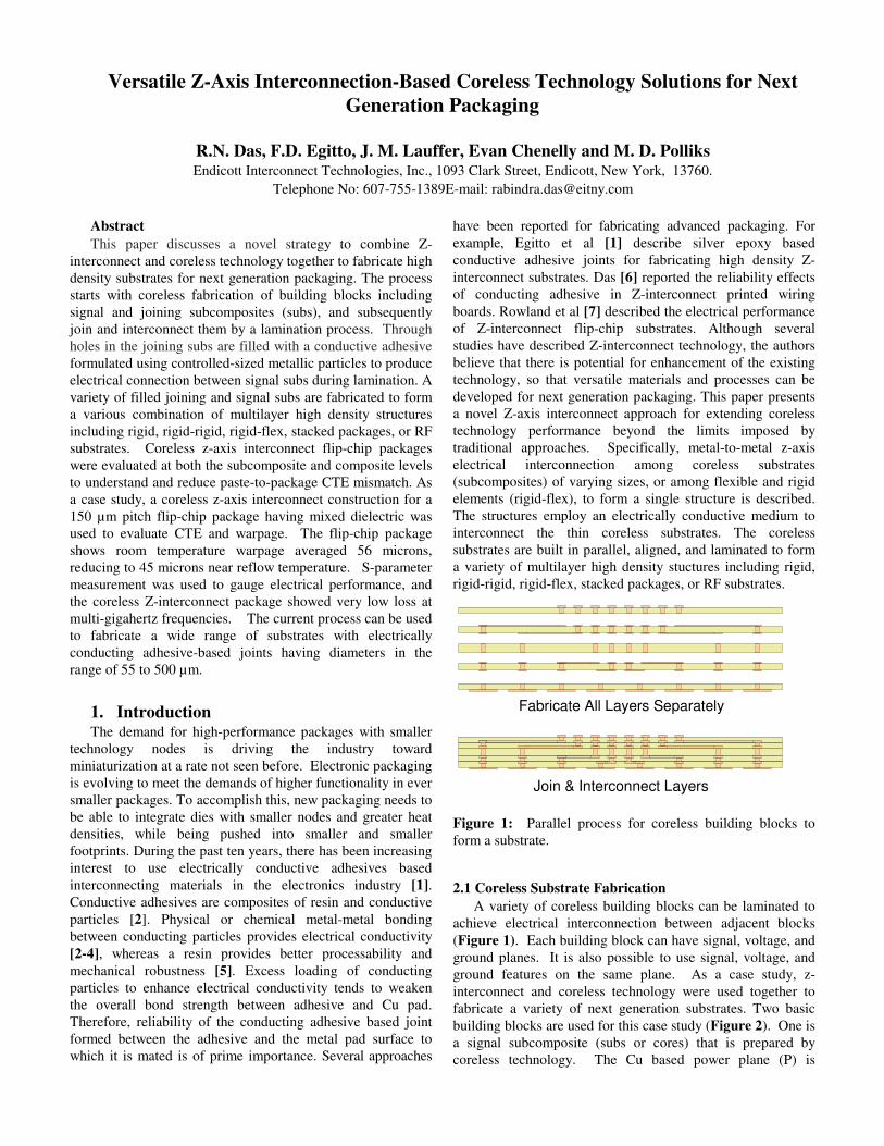
Versatile Z-Axis Interconnection-Based Coreless Technology Solutions for Next Generation Packaging R.N. Das, F.D. Egitto, J. M. Lauffer, Evan Chenelly and M. D. Polliks Endicott Interconnect Technologies, Inc., 1093 Clark Street, Endicott, New York, 13760. Telephone No: 607-755-1389E-mail: [email protected] Abstract This paper discusses a novel strategy to combine Z- interconnect and coreless technology together to fabricate high density substrates for next generation packaging. The process starts with coreless fabrication of building blocks including signal and joining subcomposites (subs), and subsequently join and interconnect them by a lamination process. Through holes in the joining subs are filled with a conductive adhesive formulated using controlled-sized metallic particles to produce electrical connection between signal subs during lamination. A variety of filled joining and signal subs are fabricated to form a various combination of multilayer high density structures including rigid, rigid-rigid, rigid-flex, stacked packages, or RF substrates. Coreless z-axis interconnect flip-chip packages were evaluated at both the subcomposite and composite levels to understand and reduce paste-to-package CTE mismatch. As a case study, a coreless z-axis interconnect construction for a 150 μm pitch flip-chip package having mixed dielectric was used to evaluate CTE and warpage. The flip-chip package shows room temperature warpage averaged 56 microns, reducing to 45 microns near reflow temperature. S-parameter measurement was used to gauge electrical performance, and the coreless Z-interconnect package showed very low loss at multi-gigahertz frequencies. The current process can be used to fabricate a wide range of substrates with electrically conducting adhesive-based joints having diameters in the range of 55 to 500 μm. 1. Introduction The demand for high-performance packages with smaller technology nodes is driving the industry toward miniaturization at a rate not seen before. Electronic packaging is evolving to meet the demands of higher functionality in ever smaller packages. To accomplish this, new packaging needs to be able to integrate dies with smaller nodes and greater heat densities, while being pushed into smaller and smaller footprints. During the past ten years, there has been increasing interest to use electrically conductive adhesives based interconnecting materials in the electronics industry [1]. Conductive adhesives are composites of resin and conductive particles [2]. Physical or chemical metal-metal bonding between conducting particles provides electrical conductivity [2-4], whereas a resin provides better processability and mechanical robustness [5]. Excess loading of conducting particles to enhance electrical conductivity tends to weaken the overall bond strength between adhesive and Cu pad. Therefore, reliability of the conducting adhesive based joint formed between the adhesive and the metal pad surface to which it is mated is of prime importance. Several approaches have been reported for fabricating advanced packaging. For example, Egitto et al [1] describe silver epoxy based conductive adhesive joints for fabricating high density Z- interconnect substrates. Das [6] reported the reliability effects of conducting adhesive in Z-interconnect printed wiring boards. Rowland et al [7] described the electrical performance of Z-interconnect flip-chip substrates. Although several studies have described Z-interconnect technology, the authors believe that there is potential for enhancement of the existing technology, so that versatile materials and processes can be developed for next generation packaging. This paper presents a novel Z-axis interconnect approach for extending coreless technology performance beyond the limits imposed by traditional approaches. Specifically, metal-to-metal z-axis electrical interconnection among coreless substrates (subcomposites) of varying sizes, or among flexible and rigid elements (rigid-flex), to form a single structure is described. The structures employ an electrically conductive medium to interconnect the thin coreless substrates. The coreless substrates are built in parallel, aligned, and laminated to form a variety of multilayer high density stuctures including rigid, rigid-rigid, rigid-flex, stacked packages, or RF substrates. Figure 1: Parallel process for coreless building blocks to form a substrate. 2.1 Coreless Substrate Fabrication A variety of coreless building blocks can be laminated to achieve electrical interconnection between adjacent blocks (Figure 1). Each building block can have signal, voltage, and ground planes. It is also possible to use signal, voltage, and ground features on the same plane. As a case study, z- interconnect and coreless technology were used together to fabricate a variety of next generation substrates. Two basic building blocks are used for this case study (Figure 2). One is a signal subcomposite (subs or cores) that is prepared by coreless technology. The Cu based power plane (P) is Fabricate All Layers Separately Join & Interconnect Layers
-
Upload
trinhtuong -
Category
Documents
-
view
218 -
download
0
Transcript of Versatile Z-Axis Interconnection-Based Coreless Technology...
Versatile Z-Axis Interconnection-Based Coreless Technology Solutions for Next Generation Packaging
R.N. Das, F.D. Egitto, J. M. Lauffer, Evan Chenelly and M. D. Polliks Endicott Interconnect Technologies, Inc., 1093 Clark Street, Endicott, New York, 13760.
Telephone No: 607-755-1389E-mail: [email protected] Abstract This paper discusses a novel strategy to combine Z-
interconnect and coreless technology together to fabricate high density substrates for next generation packaging. The process starts with coreless fabrication of building blocks including signal and joining subcomposites (subs), and subsequently join and interconnect them by a lamination process. Through holes in the joining subs are filled with a conductive adhesive formulated using controlled-sized metallic particles to produce electrical connection between signal subs during lamination. A variety of filled joining and signal subs are fabricated to form a various combination of multilayer high density structures including rigid, rigid-rigid, rigid-flex, stacked packages, or RF substrates. Coreless z-axis interconnect flip-chip packages were evaluated at both the subcomposite and composite levels to understand and reduce paste-to-package CTE mismatch. As a case study, a coreless z-axis interconnect construction for a 150 µm pitch flip-chip package having mixed dielectric was used to evaluate CTE and warpage. The flip-chip package shows room temperature warpage averaged 56 microns, reducing to 45 microns near reflow temperature. S-parameter measurement was used to gauge electrical performance, and the coreless Z-interconnect package showed very low loss at multi-gigahertz frequencies. The current process can be used to fabricate a wide range of substrates with electrically conducting adhesive-based joints having diameters in the range of 55 to 500 µm.
1. Introduction The demand for high-performance packages with smaller
technology nodes is driving the industry toward miniaturization at a rate not seen before. Electronic packaging is evolving to meet the demands of higher functionality in ever smaller packages. To accomplish this, new packaging needs to be able to integrate dies with smaller nodes and greater heat densities, while being pushed into smaller and smaller footprints. During the past ten years, there has been increasing interest to use electrically conductive adhesives based interconnecting materials in the electronics industry [1]. Conductive adhesives are composites of resin and conductive particles [2]. Physical or chemical metal-metal bonding between conducting particles provides electrical conductivity [2-4], whereas a resin provides better processability and mechanical robustness [5]. Excess loading of conducting particles to enhance electrical conductivity tends to weaken the overall bond strength between adhesive and Cu pad. Therefore, reliability of the conducting adhesive based joint formed between the adhesive and the metal pad surface to which it is mated is of prime importance. Several approaches
have been reported for fabricating advanced packaging. For example, Egitto et al [1] describe silver epoxy based conductive adhesive joints for fabricating high density Z-interconnect substrates. Das [6] reported the reliability effects of conducting adhesive in Z-interconnect printed wiring boards. Rowland et al [7] described the electrical performance of Z-interconnect flip-chip substrates. Although several studies have described Z-interconnect technology, the authors believe that there is potential for enhancement of the existing technology, so that versatile materials and processes can be developed for next generation packaging. This paper presents a novel Z-axis interconnect approach for extending coreless technology performance beyond the limits imposed by traditional approaches. Specifically, metal-to-metal z-axis electrical interconnection among coreless substrates (subcomposites) of varying sizes, or among flexible and rigid elements (rigid-flex), to form a single structure is described. The structures employ an electrically conductive medium to interconnect the thin coreless substrates. The coreless substrates are built in parallel, aligned, and laminated to form a variety of multilayer high density stuctures including rigid, rigid-rigid, rigid-flex, stacked packages, or RF substrates. Figure 1: Parallel process for coreless building blocks to form a substrate.
2.1 Coreless Substrate Fabrication A variety of coreless building blocks can be laminated to
achieve electrical interconnection between adjacent blocks (Figure 1). Each building block can have signal, voltage, and ground planes. It is also possible to use signal, voltage, and ground features on the same plane. As a case study, z-interconnect and coreless technology were used together to fabricate a variety of next generation substrates. Two basic building blocks are used for this case study (Figure 2). One is a signal subcomposite (subs or cores) that is prepared by coreless technology. The Cu based power plane (P) is
Fabricate All Layers Separately
Join & Interconnect Layers
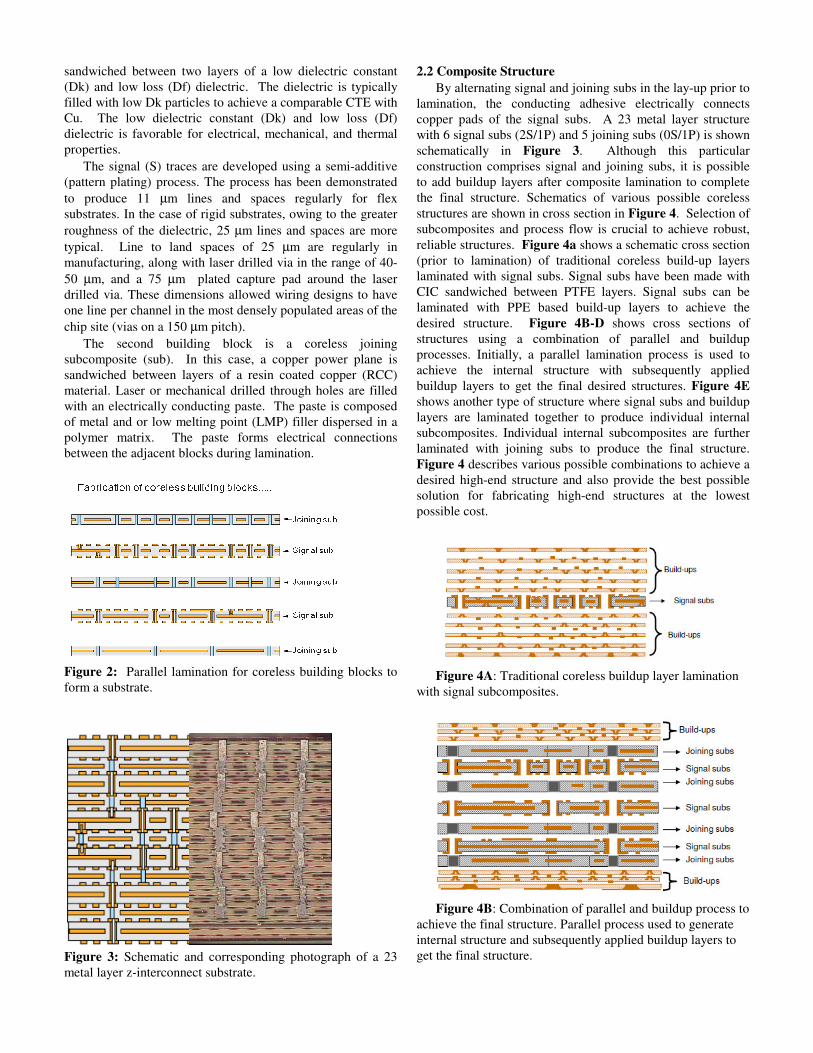
sandwiched between two layers of a low dielectric constant (Dk) and low loss (Df) dielectric. The dielectric is typically filled with low Dk particles to achieve a comparable CTE with Cu. The low dielectric constant (Dk) and low loss (Df) dielectric is favorable for electrical, mechanical, and thermal properties.
The signal (S) traces are developed using a semi-additive (pattern plating) process. The process has been demonstrated to produce 11 µm lines and spaces regularly for flex substrates. In the case of rigid substrates, owing to the greater roughness of the dielectric, 25 µm lines and spaces are more typical. Line to land spaces of 25 µm are regularly in manufacturing, along with laser drilled via in the range of 40-50 µm, and a 75 µm plated capture pad around the laser drilled via. These dimensions allowed wiring designs to have one line per channel in the most densely populated areas of the chip site (vias on a 150 µm pitch).
The second building block is a coreless joining subcomposite (sub). In this case, a copper power plane is sandwiched between layers of a resin coated copper (RCC) material. Laser or mechanical drilled through holes are filled with an electrically conducting paste. The paste is composed of metal and or low melting point (LMP) filler dispersed in a polymer matrix. The paste forms electrical connections between the adjacent blocks during lamination.
Figure 2: Parallel lamination for coreless building blocks to form a substrate.
Figure 3: Schematic and corresponding photograph of a 23 metal layer z-interconnect substrate.
2.2 Composite Structure By alternating signal and joining subs in the lay-up prior to
lamination, the conducting adhesive electrically connects copper pads of the signal subs. A 23 metal layer structure with 6 signal subs (2S/1P) and 5 joining subs (0S/1P) is shown schematically in Figure 3. Although this particular construction comprises signal and joining subs, it is possible to add buildup layers after composite lamination to complete the final structure. Schematics of various possible coreless structures are shown in cross section in Figure 4. Selection of subcomposites and process flow is crucial to achieve robust, reliable structures. Figure 4a shows a schematic cross section (prior to lamination) of traditional coreless build-up layers laminated with signal subs. Signal subs have been made with CIC sandwiched between PTFE layers. Signal subs can be laminated with PPE based build-up layers to achieve the desired structure. Figure 4B-D shows cross sections of structures using a combination of parallel and buildup processes. Initially, a parallel lamination process is used to achieve the internal structure with subsequently applied buildup layers to get the final desired structures. Figure 4E shows another type of structure where signal subs and buildup layers are laminated together to produce individual internal subcomposites. Individual internal subcomposites are further laminated with joining subs to produce the final structure. Figure 4 describes various possible combinations to achieve a desired high-end structure and also provide the best possible solution for fabricating high-end structures at the lowest possible cost.
Figure 4A: Traditional coreless buildup layer lamination
with signal subcomposites.
Figure 4B: Combination of parallel and buildup process to
achieve the final structure. Parallel process used to generate internal structure and subsequently applied buildup layers to get the final structure.
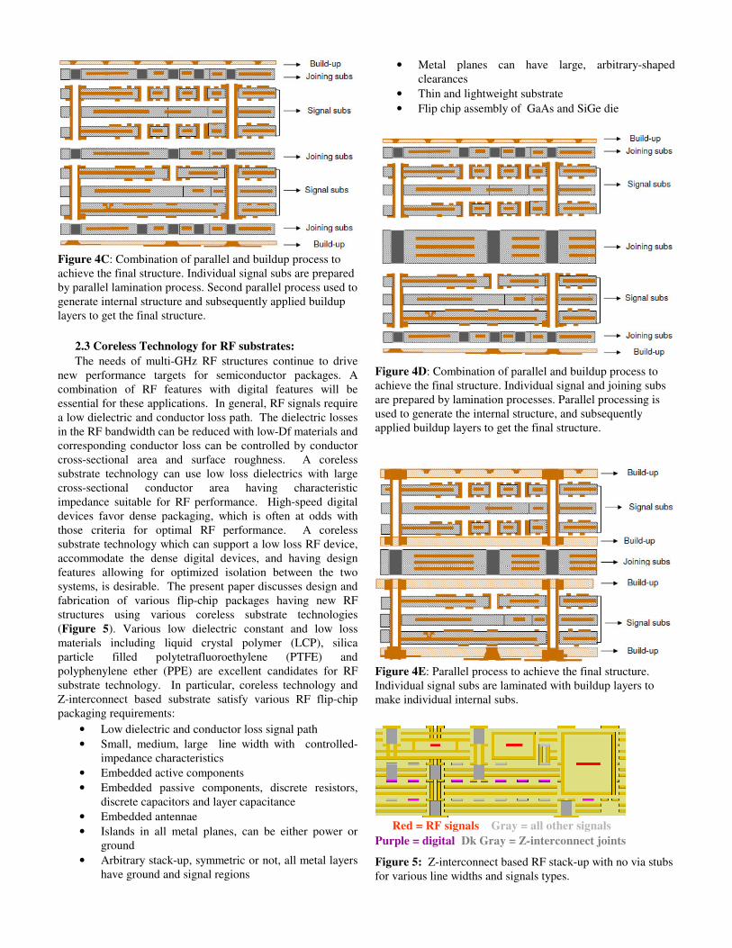
Figure 4C: Combination of parallel and buildup process to achieve the final structure. Individual signal subs are prepared by parallel lamination process. Second parallel process used to generate internal structure and subsequently applied buildup layers to get the final structure.
2.3 Coreless Technology for RF substrates: The needs of multi-GHz RF structures continue to drive
new performance targets for semiconductor packages. A combination of RF features with digital features will be essential for these applications. In general, RF signals require a low dielectric and conductor loss path. The dielectric losses in the RF bandwidth can be reduced with low-Df materials and corresponding conductor loss can be controlled by conductor cross-sectional area and surface roughness. A coreless substrate technology can use low loss dielectrics with large cross-sectional conductor area having characteristic impedance suitable for RF performance. High-speed digital devices favor dense packaging, which is often at odds with those criteria for optimal RF performance. A coreless substrate technology which can support a low loss RF device, accommodate the dense digital devices, and having design features allowing for optimized isolation between the two systems, is desirable. The present paper discusses design and fabrication of various flip-chip packages having new RF structures using various coreless substrate technologies (Figure 5). Various low dielectric constant and low loss materials including liquid crystal polymer (LCP), silica particle filled polytetrafluoroethylene (PTFE) and polyphenylene ether (PPE) are excellent candidates for RF substrate technology. In particular, coreless technology and Z-interconnect based substrate satisfy various RF flip-chip packaging requirements:
• Low dielectric and conductor loss signal path • Small, medium, large line width with controlled-
impedance characteristics • Embedded active components • Embedded passive components, discrete resistors,
discrete capacitors and layer capacitance • Embedded antennae • Islands in all metal planes, can be either power or
ground • Arbitrary stack-up, symmetric or not, all metal layers
have ground and signal regions
• Metal planes can have large, arbitrary-shaped clearances
• Thin and lightweight substrate • Flip chip assembly of GaAs and SiGe die
Figure 4D: Combination of parallel and buildup process to achieve the final structure. Individual signal and joining subs are prepared by lamination processes. Parallel processing is used to generate the internal structure, and subsequently applied buildup layers to get the final structure.
Figure 4E: Parallel process to achieve the final structure. Individual signal subs are laminated with buildup layers to make individual internal subs.
Red = RF signals Gray = all other signals
Purple = digital Dk Gray = Z-interconnect joints
Figure 5: Z-interconnect based RF stack-up with no via stubs for various line widths and signals types.
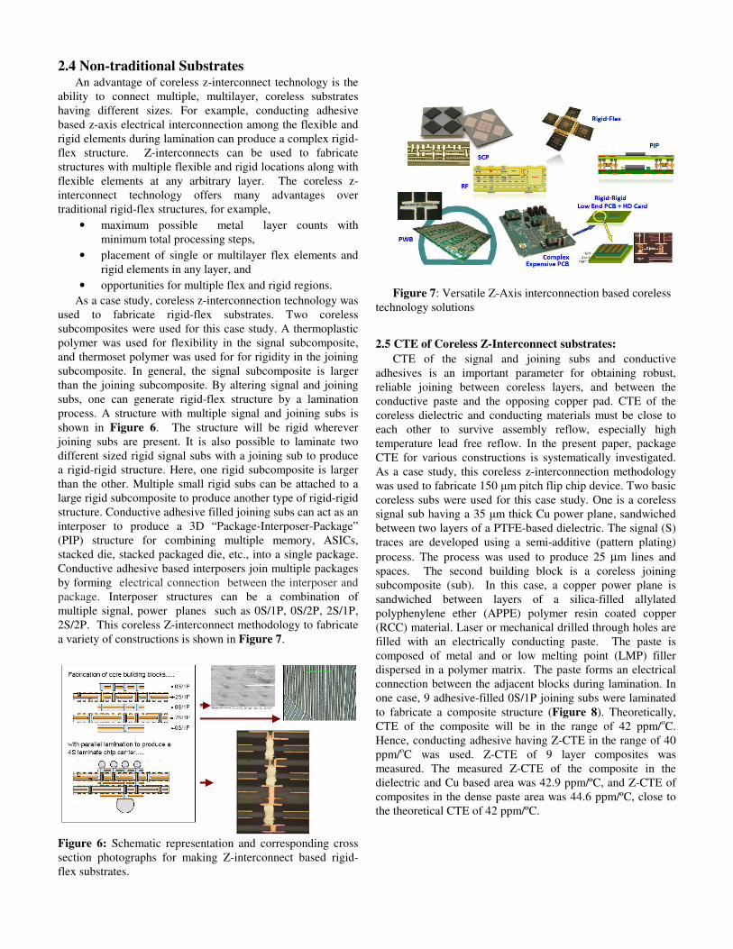
2.4 Non-traditional Substrates An advantage of coreless z-interconnect technology is the
ability to connect multiple, multilayer, coreless substrates having different sizes. For example, conducting adhesive based z-axis electrical interconnection among the flexible and rigid elements during lamination can produce a complex rigid-flex structure. Z-interconnects can be used to fabricate structures with multiple flexible and rigid locations along with flexible elements at any arbitrary layer. The coreless z-interconnect technology offers many advantages over traditional rigid-flex structures, for example,
• maximum possible metal layer counts with minimum total processing steps,
• placement of single or multilayer flex elements and rigid elements in any layer, and
• opportunities for multiple flex and rigid regions. As a case study, coreless z-interconnection technology was
used to fabricate rigid-flex substrates. Two coreless subcomposites were used for this case study. A thermoplastic polymer was used for flexibility in the signal subcomposite, and thermoset polymer was used for for rigidity in the joining subcomposite. In general, the signal subcomposite is larger than the joining subcomposite. By altering signal and joining subs, one can generate rigid-flex structure by a lamination process. A structure with multiple signal and joining subs is shown in Figure 6. The structure will be rigid wherever joining subs are present. It is also possible to laminate two different sized rigid signal subs with a joining sub to produce a rigid-rigid structure. Here, one rigid subcomposite is larger than the other. Multiple small rigid subs can be attached to a large rigid subcomposite to produce another type of rigid-rigid structure. Conductive adhesive filled joining subs can act as an interposer to produce a 3D “Package-Interposer-Package” (PIP) structure for combining multiple memory, ASICs, stacked die, stacked packaged die, etc., into a single package. Conductive adhesive based interposers join multiple packages by forming electrical connection between the interposer and package. Interposer structures can be a combination of multiple signal, power planes such as 0S/1P, 0S/2P, 2S/1P, 2S/2P. This coreless Z-interconnect methodology to fabricate a variety of constructions is shown in Figure 7.
Figure 6: Schematic representation and corresponding cross section photographs for making Z-interconnect based rigid-flex substrates.
Figure 7: Versatile Z-Axis interconnection based coreless
technology solutions
2.5 CTE of Coreless Z-Interconnect substrates: CTE of the signal and joining subs and conductive
adhesives is an important parameter for obtaining robust, reliable joining between coreless layers, and between the conductive paste and the opposing copper pad. CTE of the coreless dielectric and conducting materials must be close to each other to survive assembly reflow, especially high temperature lead free reflow. In the present paper, package CTE for various constructions is systematically investigated. As a case study, this coreless z-interconnection methodology was used to fabricate 150 �m pitch flip chip device. Two basic coreless subs were used for this case study. One is a coreless signal sub having a 35 �m thick Cu power plane, sandwiched between two layers of a PTFE-based dielectric. The signal (S) traces are developed using a semi-additive (pattern plating) process. The process was used to produce 25 µm lines and spaces. The second building block is a coreless joining subcomposite (sub). In this case, a copper power plane is sandwiched between layers of a silica-filled allylated polyphenylene ether (APPE) polymer resin coated copper (RCC) material. Laser or mechanical drilled through holes are filled with an electrically conducting paste. The paste is composed of metal and or low melting point (LMP) filler dispersed in a polymer matrix. The paste forms an electrical connection between the adjacent blocks during lamination. In one case, 9 adhesive-filled 0S/1P joining subs were laminated to fabricate a composite structure (Figure 8). Theoretically, CTE of the composite will be in the range of 42 ppm/oC. Hence, conducting adhesive having Z-CTE in the range of 40 ppm/oC was used. Z-CTE of 9 layer composites was measured. The measured Z-CTE of the composite in the dielectric and Cu based area was 42.9 ppm/ºC, and Z-CTE of composites in the dense paste area was 44.6 ppm/ºC, close to the theoretical CTE of 42 ppm/ºC.
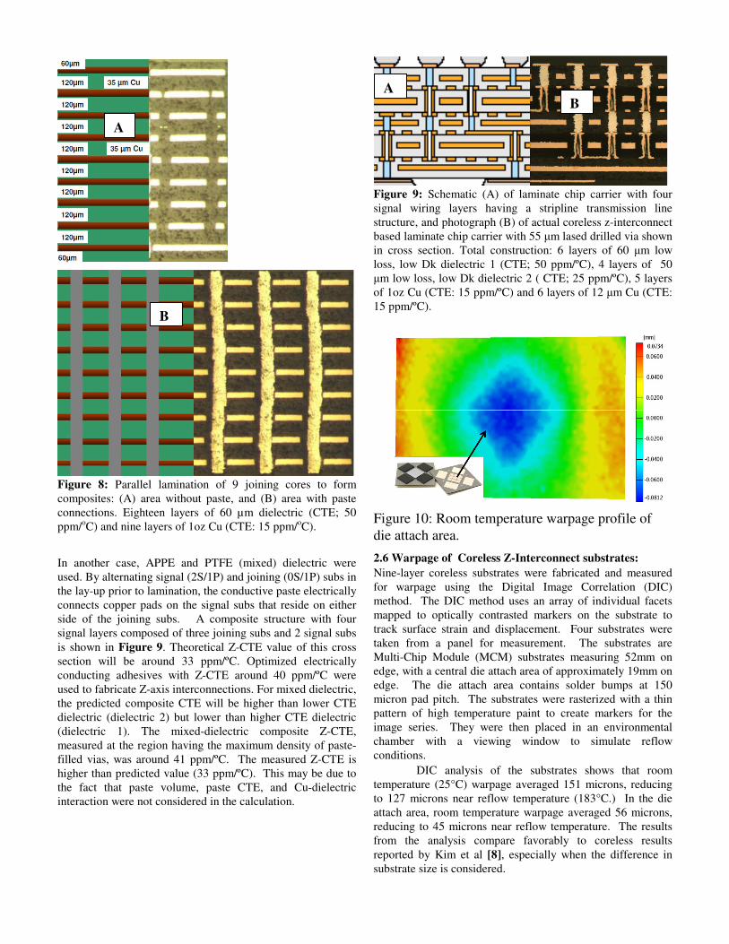
Figure 8: Parallel lamination of 9 joining cores to form composites: (A) area without paste, and (B) area with paste connections. Eighteen layers of 60 µm dielectric (CTE; 50 ppm/oC) and nine layers of 1oz Cu (CTE: 15 ppm/oC).
In another case, APPE and PTFE (mixed) dielectric were used. By alternating signal (2S/1P) and joining (0S/1P) subs in the lay-up prior to lamination, the conductive paste electrically connects copper pads on the signal subs that reside on either side of the joining subs. A composite structure with four signal layers composed of three joining subs and 2 signal subs is shown in Figure 9. Theoretical Z-CTE value of this cross section will be around 33 ppm/ºC. Optimized electrically conducting adhesives with Z-CTE around 40 ppm/ºC were used to fabricate Z-axis interconnections. For mixed dielectric, the predicted composite CTE will be higher than lower CTE dielectric (dielectric 2) but lower than higher CTE dielectric (dielectric 1). The mixed-dielectric composite Z-CTE, measured at the region having the maximum density of paste-filled vias, was around 41 ppm/ºC. The measured Z-CTE is higher than predicted value (33 ppm/ºC). This may be due to the fact that paste volume, paste CTE, and Cu-dielectric interaction were not considered in the calculation.
Figure 9: Schematic (A) of laminate chip carrier with four signal wiring layers having a stripline transmission line structure, and photograph (B) of actual coreless z-interconnect based laminate chip carrier with 55 �m lased drilled via shown in cross section. Total construction: 6 layers of 60 �m low loss, low Dk dielectric 1 (CTE; 50 ppm/ºC), 4 layers of 50 �m low loss, low Dk dielectric 2 ( CTE; 25 ppm/ºC), 5 layers of 1oz Cu (CTE: 15 ppm/ºC) and 6 layers of 12 �m Cu (CTE: 15 ppm/ºC).
Figure 10: Room temperature warpage profile of die attach area.
2.6 Warpage of Coreless Z-Interconnect substrates: Nine-layer coreless substrates were fabricated and measured for warpage using the Digital Image Correlation (DIC) method. The DIC method uses an array of individual facets mapped to optically contrasted markers on the substrate to track surface strain and displacement. Four substrates were taken from a panel for measurement. The substrates are Multi-Chip Module (MCM) substrates measuring 52mm on edge, with a central die attach area of approximately 19mm on edge. The die attach area contains solder bumps at 150 micron pad pitch. The substrates were rasterized with a thin pattern of high temperature paint to create markers for the image series. They were then placed in an environmental chamber with a viewing window to simulate reflow conditions.
DIC analysis of the substrates shows that room temperature (25°C) warpage averaged 151 microns, reducing to 127 microns near reflow temperature (183°C.) In the die attach area, room temperature warpage averaged 56 microns, reducing to 45 microns near reflow temperature. The results from the analysis compare favorably to coreless results reported by Kim et al [8], especially when the difference in substrate size is considered.
B
A
B
A
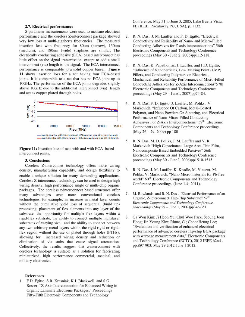
2.7. Electrical performance: S-parameter measurements were used to measure electrical
performance and the coreless Z-interconnect package showed very low loss at multi-gigahertz frequencies. The measured insertion loss with frequency for 80um (narrow), 130um (medium), and 180um (wide) striplines are similar. The electrically conducting adhesive (ECA) based interconnect has little effect on the signal transmission, except to add a small interconnect (via) length to the signal. The ECA interconnect performance is comparable to a solid copper barrel. Figure 11 shows insertion loss for a net having four ECA-based joints. It is comparable to a net that has no ECA joint up to 10GHz. The performance of the ECA joints degrades slightly above 10GHz due to the additional interconnect (via) length and act as copper plated through-holes.
Figure 11: Insertion loss of nets with and with ECA based interconnect joints.
3. Conclusions Coreless Z-interconnet technology offers more wiring
density, manufacturing capability, and design flexibility to enable a unique solution for many demanding applications. Coreless Z-interconnect technology can be used to design high wiring density, high performance single or multi-chip organic packages. The coreless z-interconnect based structures offer many advantages over more conventional coreless technologies, for example, an increase in metal layer counts without the cumulative yield loss of sequential (build up) processing, placement of flex elements into any layer of the substrate, the opportunity for multiple flex layers within a rigid-flex substrate, the ability to connect multiple multilayer substrates of varying size, and the ability to connect between any two arbitrary metal layers within the rigid-rigid or rigid-flex region without the use of plated through holes (PTHs), allowing for increased wiring density and reduction or elimination of via stubs that cause signal attenuation. Collectively, the results suggest that z-interconnect with coreless technology is suitable as a solution for fabricating miniaturized, high performance commercial, medical, and military electronics.
References 1. F.D. Egitto, S.R. Krasniak, K.J. Blackwell, and S.G.
Rosser, “Z-Axis Interconnection for Enhanced Wiring in Organic Laminate Electronic Packages,” Proceedings Fifty-Fifth Electronic Components and Technology
Conference, May 31 to June 3, 2005, Lake Buena Vista, FL (IEEE, Piscataway, NJ, USA), p. 1132.]
2. R. N. Das, J. M. Lauffer and F. D. Egitto, “Electrical
Conductivity and Reliability of Nano- and Micro-Filled Conducting Adhesives for Z-axis interconnections” 56th Electronic Components and Technology Conference proceedings (May 30 - June 2, 2006)pp112-118.
3. R. N. Das, K. Papathomas, J. Lauffer, and F.D. Egitto,
“Influence of Nanoparticles, Low Melting Point (LMP) Fillers, and Conducting Polymers on Electrical, Mechanical, and Reliability Performance of Micro-Filled Conducting Adhesives for Z-Axis Interconnections”57th Electronic Components and Technology Conference proceedings (May 29 – June1, 2007)pp74-84.
4. R. N. Das, F. D. Egitto, J. Lauffer, M. Poliks, V.
Markovich, “Influence Of Carbon, Metal-Coated Polymer, and Nano Powders On Sintering, and Electrical Performance of Nano-Micro-Filled Conducting Adhesives For Z-Axis Interconnections” 59th Electronic Components and Technology Conference proceedings , (May 26 – 29, 2009) pp 180
5. R. N. Das, M. D. Poliks, J. M. Lauffer and V. R.
Markovich “High Capacitance, Large Area-Thin Film, Nanocomposite Based Embedded Passives” 56th Electronic Components and Technology Conference proceedings (May 30 - June2, 2006)pp1510-1515
6. R. N. Das, J. M. Lauffer, K. Knadle, M. Vincent, M. Poliks, V. Markovich, “Nano Micro materials for Pb-free world” 60th Electronic Components and Technology Conference proceedings, (June 1-4, 2011).
7. M. Rowlands and R. N. Das , “Electrical Performance of an
Organic, Z-interconnect, Flip-Chip Substrate” 57th Electronic Components and Technology Conference proceedings (May 29 – June 1, 2007)pp346-351
8. Ga Won Kim; Ji Heon Yu; Chul Woo Park; Seoung Joon
Hong; Jin Young Kim; Rinne, G.; ChoonHeung Lee; "Evaluation and verification of enhanced electrical performance of advanced coreless flip-chip BGA package with warpage measurement data," Electronic Components and Technology Conference (ECTC), 2012 IEEE 62nd , pp.897-903, May 29 2012-June 1 2012.