
Vason P. Srini and Linda G. Bushnell Computer Science ... · Vason P. Srini and Linda G. Bushnell...
54
A Crossbar System for Multiprocessors Vason P. Srini and Linda G. Bushnell Computer Science Division, EECS University of California Berkeley, CA 94720 ABSTRACT Inexpensive multiprocessor systems that obtain notable improvement in performance over sequen- tial processors are currently under development at U.C. Berkeley. We are describing a crossbar system, an interconnection network, as a component of a multiprocessor system that may be used for experimen- tation with different processor architectures. For instance, one may wish to experiment with (1) intercon- necting computing nodes, which contain processors, memory, and caches and (2) connecting processors to memory modules in a "dance hall" configuration. The crossbar system is based on a single bit-slice 16x16 crossbar chip with low latency, i.e., less than 50 ns of delay using a 2 micron static CMOS tech- nology. The chip is designed so that it can be implemented in CMOS orEDFL GaAs. We used three dif- ferent tools to develop this chip: (1) Lager Tools, (2) NCR and Mentor Graphics tools, and (3) Tim- berwolfe standard-cell tools. By stacking 33 of these chips, a crossbar system has been designed that interconnects sixteen processing elements (PE) for transferring 32 bits of data and address with one-cycle read/write capability, providing there is no contention between PEs. If a conflict occurs, a tree arbiter impartially selects a PE. A printed circuit board (PCB) version of the crossbar system has also been designed. This multilayer PCB acts as a backplane and contains the crossbar chips on one side and VME connectors to the PEs on the other side. UCB/CSD Technical Report, October 1989
-
Upload
trinhthien -
Category
Documents
-
view
216 -
download
2
Transcript of Vason P. Srini and Linda G. Bushnell Computer Science ... · Vason P. Srini and Linda G. Bushnell...

A Crossbar System for Multiprocessors
Vason P. Srini and Linda G. Bushnell
Computer Science Division, EECS
University of California
Berkeley, CA 94720
ABSTRACT
Inexpensive multiprocessor systems that obtain notable improvement in performance over sequen
tial processors are currently under development at U.C. Berkeley. We are describing a crossbar system,
an interconnection network, as a component of a multiprocessor system that may be used for experimen
tation with different processor architectures. For instance, one may wish to experiment with (1) intercon
necting computing nodes, which contain processors, memory, and caches and (2) connecting processors
to memory modules in a "dance hall" configuration. The crossbar system is based on a single bit-slice
16x16 crossbar chip with low latency, i.e., less than 50 ns of delay using a 2 micron static CMOS tech
nology. The chip is designed so that it can be implemented in CMOS orEDFL GaAs. We used three dif
ferent tools to develop this chip: (1) Lager Tools, (2) NCR and Mentor Graphics tools, and (3) Tim
berwolfe standard-cell tools. By stacking 33 of these chips, a crossbar system has been designed that
interconnects sixteen processing elements (PE) for transferring 32 bits of data and address with one-cycle
read/write capability, providing there is no contention between PEs. If a conflict occurs, a tree arbiter
impartially selects a PE. A printed circuit board (PCB) version of the crossbar system has also been
designed. This multilayer PCB acts as a backplane and contains the crossbar chips on one side and VME
connectors to the PEs on the other side.
UCB/CSD Technical Report, October 1989

Report Documentation Page Form ApprovedOMB No. 0704-0188
Public reporting burden for the collection of information is estimated to average 1 hour per response, including the time for reviewing instructions, searching existing data sources, gathering andmaintaining the data needed, and completing and reviewing the collection of information. Send comments regarding this burden estimate or any other aspect of this collection of information,including suggestions for reducing this burden, to Washington Headquarters Services, Directorate for Information Operations and Reports, 1215 Jefferson Davis Highway, Suite 1204, ArlingtonVA 22202-4302. Respondents should be aware that notwithstanding any other provision of law, no person shall be subject to a penalty for failing to comply with a collection of information if itdoes not display a currently valid OMB control number.
1. REPORT DATE OCT 1989 2. REPORT TYPE
3. DATES COVERED 00-00-1989 to 00-00-1989
4. TITLE AND SUBTITLE A Crossbar System for Multiprocessors
5a. CONTRACT NUMBER
5b. GRANT NUMBER
5c. PROGRAM ELEMENT NUMBER
6. AUTHOR(S) 5d. PROJECT NUMBER
5e. TASK NUMBER
5f. WORK UNIT NUMBER
7. PERFORMING ORGANIZATION NAME(S) AND ADDRESS(ES) University of California at Berkeley,Department of ElectricalEngineering and Computer Sciences,Berkeley,CA,94720
8. PERFORMING ORGANIZATIONREPORT NUMBER
9. SPONSORING/MONITORING AGENCY NAME(S) AND ADDRESS(ES) 10. SPONSOR/MONITOR’S ACRONYM(S)
11. SPONSOR/MONITOR’S REPORT NUMBER(S)
12. DISTRIBUTION/AVAILABILITY STATEMENT Approved for public release; distribution unlimited
13. SUPPLEMENTARY NOTES
14. ABSTRACT Inexpensive multiprocessor systems that obtain notable improvement in performance over sequentialprocessors are currently under development at U.C. Berkeley. We are describing a crossbar system, aninterconnection network, as a component of a multiprocessor system that may be used for experimentationwith different processor architectures. For instance, one may wish to experiment with (1) interconnectingcomputing modes, which contain processors, memory, and caches and (2) connecting processors to memorymodules in a "dance hall" configuration. The crossbar system is based on single bit-slice 16x16 crossbarchip with low latency, i.e., less than 50ns of delay using a 2 micron static CMOS technology. The chip isdesigned so that it can be implemented in CMOS or EDFL GaAs. We used three different tools to developthis chip: (1) Lager Tools, (2) NCR and Mentor Graphics tools, and (3) Timberwolfe standard-cell tools. Bystacking 33 of these chips, a crossbar system has been designed that interconnects sixteen processingelements (PE) for transferring 32 bits of data and address with one-cycle read/write capability, providingthere is no contention between PEs. If a conflict occurs, a tree arbiter impartially selects a PE. A printedcircuit board (PCB) version of the crossbar system has also been designed. This multilayer PCB acts as abackplane and contains the crossbar chips on one side and VMe connectors to the PEs on the other side.
15. SUBJECT TERMS
16. SECURITY CLASSIFICATION OF: 17. LIMITATION OF ABSTRACT Same as
Report (SAR)
18. NUMBEROF PAGES
53
19a. NAME OFRESPONSIBLE PERSON
a. REPORT unclassified
b. ABSTRACT unclassified
c. THIS PAGE unclassified
Standard Form 298 (Rev. 8-98) Prescribed by ANSI Std Z39-18
-2-
1. Introduction
A key component of a high-performance multiprocessor system is the interconnection network
between the processors and memory modules or between processors. The bandwidth and the latency of
the interconnection network are two factors that are significant in the performance of the multiprocessor
system. For example, doubling the data path width between the processor and the memory may feasibly
double the data available to a processor for a memory read. This may result in fewer memory references
and conflicts and in more performance. Reducing the latency in the interconnection network reduces the
memory access time, which may in tum improve the effectiveness of the system. Our goal is to design an
interconnection network where bandwidth may be enlarged by increasing the width of the data path and
latency may be reduced by decreasing the gate delay.
Although crossbars have been in use in computer systems [Bur69, WuB72, WuH78], they do not
meet our bandwidth and latency requirements. For instance, the memory references in Prolog programs
do not exhibit locality usually found in Pascal or C programs. This means a processor's memory refer
ences may change from module to module in adjacent cycles. A similar situation also arises in object
oriented programs. To support this type of randomness in memory references, a dynamic crossbar with
low latency for changing switch settings is needed. We have designed [Sri88, SrD89] a single bit-slice
crossbar chip for connecting 16 processors to 32 memory modules. The switch connection in the crossbar
can change every cycle based on the memory requests from the processors. By stacking 33 of these chips,
we can have 32-bit words transferred in one cycle. The extra chip is for control. The total delay in the
chip is equivalent to the delay through 20 gates. Because of the complexity of 16x32 crossbar system, we
have also designed a simpler crossbar chip for interconnecting 16 PEs. This second crossbar system is
descri!Jed in this paper. It is easy to extend the simpler design to connect processors to memory.
Our design is different from that of other designs in the literature. It is oriented towards high perfor
mance implementation in submicron CMOS and GaAs technologies. The chip design proposed by Frank
lin [FWT82, WaF83] employs multiple stages and does not meet our latency requirements. The 16xl6
crossbar chip in the MARS [Agr87] system for connecting processors does not meet our specifications.
The arbiter used in the chip is based on positional priority, which may cause performance problems in
logic programs because of the randomness in memory references.

- 3-
Section 2 describes current multiprocessor systems for Prolog employing the crossbar. Section 3
details the crossbar chip and section 4 presents the testini! of the chip. Section 5 describes the crossbar
board. Section 6 gives some conclusions.
2. Multiprocessor System for Prolog
Several proposals for executing Prolog programs on multiple processors have appeared in the litera
ture. Two of the proposals [Bor84, WAD84] extend the stack architecture of Warren [TiW83, War83].
The stacks are allowed to spread across the processors in the shared memory multiprocessor system
[Bor84] as the parallelism grows. The AND parallelism and stream parallelism [Con83] are exploited in
this multiprocessor. The distributed system of Warren [WAD84] supports the OR parallelism [Con83] in
Prolog programs by distributing the clauses in a procedure to many processors connected to a broadcast
network. We have been experimenting with a heterogeneous, tightly coupled, multiprocessor system
[Dob86, NSD88] with special processors to execute logic programming at the control level and numeric
processing to execute arithmetic functions. A block diagram of our proposed multiprocessor is shown in
Figure 1. It employs 12 Parallel Prolog Processors (PPP) [SrD89], three floating point processors (FPP),
a general purpose processor (GPP),snooping caches (SC), caches (C), memory (M), and the crossbar. The
PPP in the figure is based on the Prolog machine (PLM), developed at Berkeley [DPD84, STN87], and
will exploit the AND, OR, and stream parallelism in Prolog programs. A static analysis of Prolog pro
grams will be done to detect the AND parallelism. One of the key components of the multiprocessor is
the crossbar. There are other multiprocessors (NECTAR, RP3, etc.) that employ crossbars. Some of the
early systems such as B6700 [Bur69] and C.mmp [WuB72] have also employed crossbars.
3. Crossbar Chip
The crossbar chip described in this paper is an interconnect-intensive and pad-limited chip. It con
tains 40,000 transistors. The pin-out of a single bit-slice 16x16 crossbar chip is shown in Figure 2. The
inputs to the chip are indicated with a triangle pointing inward; the outputs have the triangles pointing
outward. Signal names starting with a P are connected to the source PE, while signal names starting with
an M are connected to the destination PE (or memory). These signals are explained in section 5 on the
crossbar system design. The timing diagrams for read and write requests are shown in Figure 3.

-4-
3.1. Crossbar Chip Design
The physical design of the crossbar chip was done using three sets of tools. The first layout of the
chip using the OCf/VEM/Mosaico tools [Spi88] resulted in a chip with a size of 28 mm by 21 mm using
the MSU standard cells and a 2 micron CMOS technology. Since the die size exceeded our limit of 20
mm by 20 mm, no fabrication effort was made. The second attempt at layout was done using the Lager
IV tools [Bro88] and improved MSU standard cells. The die size is 20 mm by 16 mm for a 2 micron
CMOS process.
The third set of tools used in the layout process is the Mentor Graphics' Idea Station and NCR's
Tangent router. The gate level design was completed using the Idea Station. The physical design has
been completed using a 1.5 micro CMOS technology with NCR supplied standard cells. The resulting
chip has a die size of 9 mm by 9 mm. This fabrication of this design with good yield appears to be feasi
ble. The actual fabrication could use a 1.2 micron technology and thus bring the die size to 7.5 mm by
7.5 mm. The standard PGA packages with 210 leads can be used with the above die size, or a tape
automated bonding (fAB) packaging technology may be used and the die surface mounted on a PC
board. The chip is pad limited and uses metal2 quite heavily for the interconnections.
The bit-slice approach to crossbar design may cause word inconsistency problems [FWT82]. To
avoid this problem, reset pins are included in the chip. All the crossbar chips of a word can be initialized
to the same state using the reset signal coming from the PEs. Although the number of pins in a chip may
be reduced by using bidirectional data lines for the read and write operations, we decided against it to
keep the circuits simple and also to facilitate a GaAs implementation.
3.2. Crossbar Chip Components
The crossbar design has five components: decoder, arbiter, crosspoint matrix, input drivers, and
output drivers. They are shown in the first sheet of the top-level schematic for the crossbar chip in Fig
ures 4 and 5. The design details of each component are described in this section. To achieve low latency
and simplicity in circuit design, chip area has been compromised. Every component contains many
blocks, each of which has its delay estimated by running timing simulation. We iterated on the design
and added bigger drivers to reduce the time delay in the blocks.
- 5-
3.2.1. Decoder
There are sixteen 4 input to 16 output decoders per chip. Each decoder receives a 4-bit destination
PE address and a PE request signal from a source PE . At most one output of a decoder will be high,
denoting the destination PE requested by the source PE connected to it. There are many ways to design
the decoder, the simplest and slowest being to use 5 input AND gates. The nominal delay through a 5
input NAND gate for a load of 0.2pf is 5.5 ns and the delay through an inverter is 1.0 ns. Another way is
to use two levels of 3 and 2 input NAND gates and NOR gates. The nominal delay through a 3 input
NAND gate for a load of 0.2pf is 2.5 ns and the delay through a 2 input NOR gate is 2.0 ns. The two
level design has a delay of 4.5 ns compared to 6.5 ns for a one level design. We chose the two-level
design. Figures 6 through 9 show the symbols and logic of the decoder. Figure 7 is only a sample of the
decoder's schematic sheet. The Decoder Array in Figure 4 is formed by using sixteen of the decoders.
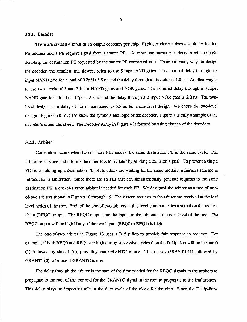
3.2.2. Arbiter
Contention occurs when two or more PEs request the same destination PE in the same cycle. The
arbiter selects one and informs the other PEs to try later by sending a collision signal. To prevent a single
PE from holding up a destination PE while others are waiting for the same module, a fairness scheme is
introduced in arbitration. Since there are 16 PEs that can simultaneously generate requests to the same
destination PE, a one-of-sixteen arbiter is needed for each PE. We designed the arbiter as a tree of one
of-two arbiters shown in Figures 10 through 15. The sixteen requests to the arbiter are received at the leaf
level nodes of the tree. Each of the one-of-two arbiters at this level communicates a signal on the request
chain (REQC) output The REQC outputs are the inputs to the arbiters at the next level of the tree. The
REQC output will be high if any of the two inputs (REQO or REQ 1) is high.
The one-of-two arbiter in Figure 13 uses a D flip-flop to provide fair response to requests. For
example, if both REQO and REQl are high during successive cycles then the D flip-flop will be in state 0
(1) followed by state 1 (0), providing that GRANTC is one. This causes GRANTO (1) followed by
GRANT I (0) to be one if GRANTC is one.
The delay through the arbiter is the sum of the time needed for the REQC signals in the arbiters to
propagate to the root of the tree and for the GRANTC signal in the root to propagate to the leaf arbiters.
This delay plays an important role in the duty cycle of the clock for the chip. Since the D flip-flops

- 6-
change state during the falling edge of the clock, the duty cycle of the clock must be greater than the pro
pagation delay from the leaves to the root of the arbiter. Table 1 shows the state table of the one_of_two
arbiter. The worst case delay (Temperature of 80 degrees Celsius and VDD = 4.5 V) for the arbiter is
used in determining the duty cycle. The grant signals coming down from the root of the tree will be
stable after clock goes low. This will allow the grant signals at the leaves to be stable when the clock is
low.
3.2.3. Crosspoint Matrix
The crosspoint matrix component, shown in Figures 16 through 21, connects the 16 PEs to each
other using 256 switches. Each switch is a combinational logic block and is shown in Figure 17. If PE i
has been selected to communicate with PE j, then the signal g_i_j will be high. This signal allows the
read, write, address, and data to be communicated to the PEs. Sixteen of these switches are grouped into
a block where a wired-or connection is used for the read, write, address, and data signals. Since the
switches are unbuffered the connections last for one cycle only, making the crossbar chip dynamic.
3.2.4. Input Drivers
The signals entering the chip from the PEs are directed to various components in the chip using
drivers. The P _SYNC unit in Figures 22 through 26 has drivers for all signals coming from the input
pads. It also supplies conflict information to the PEs.
3.2.5. Output Drivers
The read, write, address, and data signals are sent from the M_SYNC unit in Figures 27 through 30
using drivers. These signals first go to output pads and are then connected to the PEs. The pad drivers
supply 8 milliamps of current.
4. Simulating the Crossbar Chip
The complexity of the design of the crossbar chip is augmented by the need to achieve a 50 ns cycle
time. We used functional simulation to verify the data transfers from the inputs to outputs. The timing
simulation used estimated capacitances to determine the delay through the blocks.

- 7 -
The simulation efforts used a "start small" approach. The functional simulation was perfonned in
two stages. Each of the blocks of the crossbar was simulated separately, then the entire crossbar chip was
simulated. The patterns used for simulating the chip are generated by programs and used as an input to
the MG QuickSim tool. Since it was not possible to have a simulation run for each combination of
read/write requests, patterns were selected from 1, 2, 4, 8, and 16 simultaneous requests to produce con
sistent test cases.
The timing simulations programs were run for each of the blocks to calculate the delay in each
block. This allowed us to redesign some blocks by adding bigger drivers or by changing the circuits to
reduce the delay and to meet the timing constraints.
After the crossbar chip design schematics were completed and verified, we used the MG tool
Expand to transfonn the multi-level hierarchical schematics into a flat array of primitive elements consist
ing only of basic cells and wires. A basic cell is a digital component that has associated with it a com
puter program that models its functional behavior. The simulations were perfonned with the QuickSim
tool, which interactively allows for the verification of the functionality and timing of the design. All
simulation results followed specifications. The stimulants for the one of two arbiter and its output is
shown in Table 2. The input and outputs of the one of 16 arbiter is shown in Table 3.
5. Crossbar System
An essential part of the multiprocessor system in Figure 1 is the crossbar interconnection network.
This crossbar system employs the crossbar bit-slice chip and was designed for interconnecting 16 PEs.
The system is interconnect intensive because each PE has two groups of 80 signals, and is a difficult one
to simulate because of its size. There are over 2500 wires, 33 chips with 210 pins each, 288 driver chips
with support for driving 2304 signals, and 32 VME DIN connectors.
To manage this wiring complexity, two approaches were explored. One approach used the wafer
scale integration (WSI) and innovations in packaging technology. The MIT-Lincoln Laboratory has
developed a WSI technique using laser cutting and welding. The technique has been demonstrated by
building two signal processors on wafers [Raf85]. Using the WSI technique it is possible to interconnect
9 crossbar chips on a 10 em ( 4 inch) diameter wafer using a redundancy factor of four. The redundancy
will be used to bypass faulty chips. A new wafer packaging technique that will allow connections to

- 8 -
1200 pads on a wafer is needed for this approach to succeed along with software tools for programming
the wafer.
The second approach is to use. tape automated bonding (TAB) for the chips and surface mount the
dies on a multilayer PC board. The latter approach is pursued in this research project.
In this design, the latency of the crossbar system is the delay through a single chip. Each PE sup
plies a 4-bit module address to the crossbar chip. The address within the module, data to be communi
cated, read operation, and write operation are specified by separate pins. Each PE receives address, data,
read, and write signals on separate pins from a crossbar chip. Iftwo or more PE address the same destina
tion PE, one will be selected by the chip. The other PE will be sent conflict information. Each PE has a
collision pin to receive the above information, 32 address pins, 32 data pins, four module indicator pins,
and eight control pins to the crossbar system. The control pins are used to design the access protocol of
VME.
5.1. Crossbar Board Design
In this section, we will describe how we connected 33 bit-slice crossbar chips to create the crossbar
system that interconnects sixteen PEs for 32 bits of data and control communication. The multilayer
crossbar board uses 33 crossbar chips, 32 VME J1Pl/J2P2 connector pairs, and 288 driver chips to build
a backplane for the multiprocessor system. The crossbar chips are placed on the component side of the
board, while the VME connectors are on the connector side.
Figure 31 shows the top sheet of the crossbar board, which contains 33 crossbar chips labeled from
zero to 32 to represent the data/address bits zero through 31 and the read/write collision signals control
chip, respectively. To provide the required drive for the control signals, each signal is split into two sig
nals via a driver. One signal goes to crossbar chips zero through sixteen; the other goes to chips seven
teen through 32. A "Z" is added to the signal name attached to chips seventeen through 32. The control
pins are used to design the protocol for communication between PEs using the VME access protocol.
Figure 32 shows the second sheet of the crossbar board, which contains the VME connectors for the
sixteen PEs. We used a frame (for I= 0 to 15) around the logic to represent the sixteen PEs to simplify
the Neted drawing. For one PE, we used the V:ME connector pair Jl/P1 and J2/P2 along with 144 drivers
(74F244) in 18 chips. On the Jl/P1 connector, we used pins IRQ3* to IRQ7* for the PE control signals

-9-
(four for processor module address and one for processor request). These are supposed to be used for
interrupt requests, but we decided that only IRQ 1 * and IRQ2* are needed for interrupts in our design.
We used many 74F244 drivers to guarantee good signal strength at the destination. For example,
the signal MDJ(I) for bit J (J = 0 to 31) and PE I (I = 0 to 15) shown in Figure 32 is sent from PE I
through the J2/P2 VME connector to a 74F244 driver before it is sent to crossbar chip J. The drivers are
controlled by the 32nd bit of the signals, i.e., MD32(1) controls the drivers that send the MDJ(I) (J = 0 to
31) from crossbar J toPE I. The signals PDIN and PD are multiplexed by using two drivers controlled by
PDIN32(1) and PD32(1). The signals MDOT and MD are similarly multiplexed. The signals MA and PA
did not need drivers, so they come directly out of the crossbar and VME connectors.
Figure 33 shows the inputs and outputs of aPE. The module request signals P0(3:0) to P15(3:0) are
sent from PEs zero to fifteen, respectively, to each of the bit-slice crossbar chips. These signals are used
to request a destination PE. For instance, PE zero can send the 4-bit address P0(3:0) of a desired destina
tion PE to all 32 crossbar chips. To drive these signals to all 32 crossbar chips, the signals are put
through two 74F244 drivers, as displayed in Figure 32 in the upper right comer. One driver's outputs are
PJ(3:0) (for J = 0 to 15 for the sixteen PEs), which go to crossbar chips zero through sixteen. The other
driver's outputs are PZJ(3:0), which go to crossbar chips seventeen through 32. This signal gave us the
most trouble when designing this schematic sheet. To use the frame (for I= 0 to 15 for the sixteen PEs),
we had to label these signals ('P' &I)(J) and ('PZ' &I)(J) (for J = 0 to 3) as shown in the upper right comer
in Figure 32. When the design is prepared for layout and routing, the MG tool Expand interprets the &
symbol to mean concatenate. If this was not done, we would have had to make a separate sheet for each
PE, complicating the design and comprehensibility.
The processor request PR(15:0) is sent from the PEs to the crossbar chips. This signal issues a
request for contacting a destination PE. For example, PR(O) is sent by PE zero to all 33 crossbar chips.
To drive this signal, it is put through a 74F244 driver, as seen in Figure 32 in the upper right comer. The
signal PR(I) (for PE I) is connected to two drivers. The outputs of the first driver are PR(J), which is sent
to crossbar chips zero to sixteen, and the output of the second driver is PRZ(J), which is sent to crossbar
chips seventeen to 32.
The processor address bus PAJ(15:0) (for J = 0 to 32 for the 32-bit address and control bit) is sent
from all PEs to the crossbar chips. The signal P AJ(I) holds the Jth bit of the 32-bit address that is sent

- 10-
from PE I to the crossbar chips. For example, PE zero sends every crossbar chip (J = 0 to 32) the bit
PAJ(O).
The processor data output bus PDJ(15:0) (for J = 0 to 32 for the 32-bit data and control bit) is sent
from all PEs to the crossbar chips. The signal PDJ(I) holds the Jth bit of the 32-bit address that is sent
from PE I to the crossbar chip J. For example, PE one sends the crossbar chip zero the bit PDO(l).
The processor data input bus PDINJ(15:0) (for J = 0 to 32 for the 32-bit data and control bit) is sent
from the crossbar chips to the PEs. The signal PDINJ(I) holds the Jth bit of the 32-bit address that is sent
from crossbar chip J to PE I. For instance, crossbar chip zero sends PE two the bit PDIN0(2).
The data from the destination PE (or memory module) MDOTJ(15:0) (for J = 0 to 32 for the 32-bit
data and control bit) is sent from the destination PE to the crossbar chips. Similarly, the data into the des
tination PE MDJ(15:0) and the destination address MAJ(l5:0) are sent from the crossbar chips to the des
tination PE.
The clock and reset signals also must be put through a driver, as displayed in Figure 32 in the upper
right hand corner, to have the necessary drive to reach all 33 crossbar chips.
To illustrate the complexity of the crossbar system, we can look at a sample scenario. Suppose that
PE 0 wants to send PE 1 32 bits of data and an address and PE 1 wants to send PE 2 data and an address
all in the same cycle. PE 0 first sends PR(O) to all crossbar chips, indicating that it wants to communicate
with another PE. It then sends the address of PE 1 in P0(3:0) to all crossbar chips. If there is no conten
tion, PE 0 sends PDJ(O) (for J = 0 to 32) to the crossbar chips, which send this 32-bit data toPE 1 in one
cycle. PE 1 receives the data as MDJ(l) (J = 0 to 32). Simultaneously, PE 1 sends PR(l) to all crossbar
chips followed by the address ofPE 2 in P1(3:0). If there are no conflicts, PE 1 sends PAJ(1) (for J = 0 to
32) to the crossbar chips, which send this 32-bit address toPE 2 as MAJ(2) (J = 0 to 32). All sixteen PEs
can be reading and writing data and addresses in the same cycle, providing there is no contention for des
tination PEs.
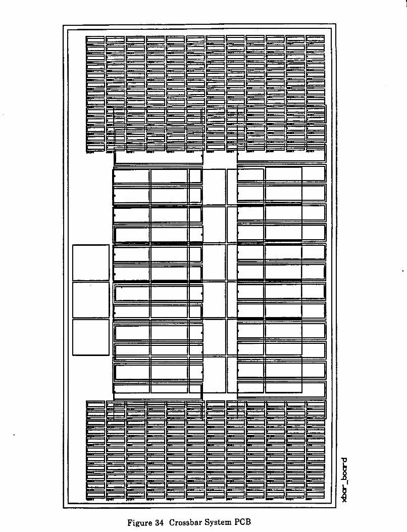
5.2. Crossbar PCB
The placed and routed PCB for the crossbar board is shown in Figure 34. The PCB measures 20 by
13 inches, has a connector side and a components side, and has eight signal layers and two power layers.
On the connector side, we placed the sixteen pairs of VME connectors, which are on the top and bottom

- 11-
of the board. The Jl/P 1 and J2/P2 connectors for PE zero are on the far left, with Jl/P 1 above J2/P2. The
connectors for PE fifteen are on the far right. On the component side, we placed the 33 crossbar chips and
the 288 drivers (74F244). The placement was done manually. We had to redo the placement a few times
with a larger board size. Although the board has two sides, there can be no overlap between the VME
connectors and the crossbar and driver components because we used through-pin PCB components. The
routing was done automatically on the Apollo's DN3000. We are using many passes of the routing algo
rithms to completely route the PCB. The backplane may be used for other general purpose systems, such
as the WARP system at Carnegie-Mellon University and the signal processing systems at UCB.
6. Conclusion
We have described the design and simulation of a bit-sliced crossbar chip and the design of a
crossbar system that interconnects processing elements. The crossbar interconnection system is the main
component of a multiprocessor system for Prolog that is currently under development at U.C. Berkeley.
The crossbar system was designed to interconnect sixteen PEs, but can be easily extended to connect six
teen processors to 32 memory modules or to interconnect 32 computing nodes.
Although this is an on going project, some initial conclusions may be drawn based on design and
simulation work. The timing simulation of the crossbar chip shows that using a 1.5 micron CMOS tech
nology a latency time of 50 ns can be achieved for the crossbar chip. This means an extra cycle for
read/write access when there is a cache miss and there are no conflicts assuming a 50 ns cache cycle time.
This is important for the parallel execution of Prolog programs, which has heavy memory traffic. Since
the miss ratios are well under five percent for many of the high performance systems, we expect no
noticeable performance degradation if the crossbar system is used.
Since the crossbar chip and the crossbar system designs are huge, the VLSI tools have to be
modified to accommodate more than 5000 wires and chips with more than 200 pins. This has motivated
tool designers and builders to pay attention to memory management and space allocation per process.

- 12-
Acknowledgement
We are thankful to Tara Weber for doing parts of the simulation of the crossbar chip. The help pro
vided by Andrea Casotto, Jan Rabey, Bob Brodersen and members of the LageriV team in understanding
the tools while routing the blocks of the crossbar chip is appreciated. We also received help from
members of the Aquarius group in the simulation of the chip. The routing of the crossbar chip at NCR
Fort Collins was done by a team headed by Harold Crafts, Robin Steele, and Dan Ellsworth.
This work was sponsored by the Defense Advanced Research Projects Agency (DoD) and moni
tored by the Office of Naval Research under Contract No. N00014-88-0579 through the Electronics
Research Laboratory, University of California, Berkeley. This research was also partially funded by NCR
Dayton, Ohio and MICRO project of the state of California.
References
[Agr87]
[Bor84]
P. Agrawal, MARS: A Multiprocessor-based Programmable Accelerator, IEEE Design &
Test of Computers 5, 4 (October 1987), 28-36.
P. Borgwardt, Parallel Prolog using Stack Segments on Shared-Memory Multiprocessors,
Proceedings of the 1984 International Symposium on Logic Programming, Atlantic City,
New Jersey, February 1984.
[Bro88] R. W. Brodersen, LageriV Distribution 1.0 Silicon Assembly System Manual, Electronics
Research Laboratory, University of California, Berkeley, June 1988.
[Bur69] Burroughs Corporation, Burroughs B6700 Reference Manual, 1969.
[Con83] J. S. Conery, The AND/OR Process Model for Parallel Interpretation of Logic Programs,
University of California, Irvine, CA, June 1983. Ph.D. Thesis.
[DPD84] T. Dobry, Y. Patt and A.M. Despain, Design Decisions Influencing the Microarchitecture
For A Prolog Machine, Proceedings of the MICRO 17, October 1984.
[Dob86] T. Dobry, Extending a Prolog Machine for Parallel Execution, Proceedings of Hawaii
International Conference on System Sciences, Honolulu, Hawaii, January 1986.

- 13-
[FWT82] M. A. Franklin, D. F. Warm and W. J. Thomas, Pin Limitations and partitioning of VLSI
Interconnection Networks, IEEE Transactions on Computers C-31, 11 (November 1982).
[NSD88] T. M. Nguyen, V. P. Srini and·A. M. Despain, A Two-Tier Memory Architecture for High
Performance Multiprocessor Systems, Proceedings of the International Conference on Super
Computing, Saint-Malo, France, July 1988.
[Raf85] J. I. Raffel, A Wafer-Scale Digital Integrator Using Restructurable VLSI, IEEE Journal of
Solid-State Circuits SC-20, 1 (February 1985).
[Spi88] R. Spickelmier, Oct Tools Distribution 2.1, Electronics Research Laboratory, University of
California, Berkeley, March 1988.
[STN87] V. P. Srini, J. T. Tam, T. M. Nguyen, Y. N. Patt and A. M. Despain, A CMOS Chip for
Prolog, Proceedings of the International Conference on Computer Design, Rye Town, NY,
October 1987.
[Sri88] V. P. Srini, An Improved Bit-sliced Cross-connect Chip for use in Multiprocessor Computer
Systems, Patent Application, University of California, Berkeley, October 1988.
[SrD89] V. P. Srini and A. M. Despain, Multiprocessor Research for Prolog, Proceedings of the State
of California M/CR0-1988 Report, January 1989.
[TiW83] E. Tick and D. H. D. Warren, Towards a Pipelined Prolog Processor, SRI International,
Menlo Park, CA, August 1983. Technical Report.
[WaF83] D. F. Warm and M. A. Franklin, Asynchronous and Clocked Control Structure for VLSI
Based Interconnection Networks, IEEE Transactions on Computers C-31, 3 (March 1983).
[War83] D. H. D. Warren, An Abstract Prolog Instruction Set, SRI International, Menlo Park, CA,
1983. Technical Report.
[W AD84] D. S. Warren, M. Ahamad, S. K. Debray and L. V. Kale, Executing Distributed Prolog
Programs on a Broadcast Network., Proceedings of the 1984 International Symposium on
Logic Programming, Atlantic City, NJ, February 1984.
[WuB72] W. A. Wulf and C. G. Bell, C.mmp- A Multi Miniprocessor, Proceedings of the AFIPS Fall
Joint Computer Conference, Montvale, New Jersey, 1972.

- 14-
[WuH78] W. A. Wulf and S. P. Harbison, Reflections in a Pool of Processors, Proceedings of the
AFIPS Fall Joint Computer Conference, Montvale, New Jersey, 1978.

Table I State Transition Table for one of two Arbiter
Present INPUTS Next OUTPUTS State RQO RQ1 GRC State GRO GR1 RQC
0 0 0 0 0 0 0 0 0 1 0 1 0 1 0 1 0 1 1 1 1 0 1 1 0 0 0 0 0 0 0 0 1 0 0 0 0 0 0 1 1 1 0 1 1 1 0 0 0 1 0 0 0 1 0 1 1 1 0 1 1 1 1 1 1 0 1 0 1 1 0 1 0 0 1 0 0 1 1 0 0 0 1 1 0 1 0 1 0 1

Table 2 Simulation Results of One of Two Aribiter
TIME "REQO "REQC "CLK "SETB "REQ1 "GRANTO "CLKB
"GRANTC "GRANT1 "RESETB 0.0 Xr Xr Xr X X X 0 1 0 1
55.0 Xr Xr Xr X 0 0 1 0 0 1 90.0 Xr Xr Xr X X X 0 1 1 1
100.0 0 0 0 X X X 0 1 1 1 200.0 0 0 0 0 0 0 0 1 0 1
4100.0 1 1 1 1 1 0 0 1 0 1 4155.0 1 1 1 1 0 0 1 0 0 1 4190.0 1 1 1 1 0 0 0 1 0 1 4200.0 1 0 1 1 0 0 0 1 1 1 4204.0 1 0 1 1 1 0 0 1 1 1 4304.0 1 1 1 1 0 1 0 1 1 1 4404.0 1 1 1 1 1 0 0 1 1 1 4504.0 1 1 1 1 0 1 0 1 1 1 4604.0 1 0 1 1 1 0 0 1 1 1 4704.0 0 1 1 1 0 1 0 1 1 1 4804.0 1 1 1 1 1 0 0 1 1 1 4904.0 0 1 1 1 0 1 0 1 1 1 5104.0 1 1 1 1 1 0 0 1 1 1 5204.0 1 1 1 1 0 1 0 1 1 1 5304.0 1 0 1 1 1 0 0 1 1 1 5404.0 1 1 1 1 0 1 0 1 1 1 5504.0 1 1 1 1 1 0 0 1 1 1 5600.0 1 1 1 1 0 1 0 1 1 1

Table 3 ·Input and Outputs of One of 16 Aribter
TIME "PREQ "CLK "RESET "'PGRNT "'SET
200.0 0001 0000 0 0 0 212.0 0001 0001 0 0 0 300.0 0002 0001 0 0 0 302.0 0002 0002 0 0 0 400.0 0004 0002 0 0 0 407.0 0004 0004 0 0 0 500.0 0008 0004 0 0 0 502.0 0008 0008 0 0 0 600.0 0009 0008 0 0 0 607.0 0009 0001 0 0 0 755.0 0009 0008 1 0 0 790.0 0009 0008 0 0 0 855.0 0009 0001 1 0 0 955.0 0009 0008 1 0 0
1000.0 OOOA 0001 0 0 0 1004.0 OOOA 0002 0 0 0 1055.0 OOOA 0002 1 0 0 1155.0 OOOA 0008 1 0 0 1255.0 OOOA 0002 1 0 0 1355.0 OOOA 0008 1 0 0 1400.0 oooc 0002 0 0 0 7100.0 FFFF 0000 0 0 0 7113.0 FFFF 0100 0 0 0 7201.0 FFFF 0001 0 0 0 7301.0 FFFF 1000 0 0 0 7401.0 FFFF 0010 0 0 0 7501.0 FFFF 0400 0 0 0 7601.0 FFFF 0004 0 0 0 7701.0 FFFF 4000 0 0 0 7801.0 FFFF 0040 0 0 0 7901.0 FFFF 0200 0 0 0 8001.0 F?FF 0002 0 0 0 8101.0 FFFF 2000 0 0 0 8201.0 FFFF 0020 0 0 0 8301.0 FFFF 0800 0 0 0 8401.0 FFFF 0008 0 0 0 8501.0 FFFF 8000 0 0 0 8601.0 FFFF 0080 0 0 0 8701.0 FFFF 0100 0 0 0 8902.0 0000 0000 0 0 0
TIME "'PREQ "CLK "RESET "'PGRNT "'SET

Synchronization Memo0
Synchronization Bus I
I
~l I I 0 0 .8] 0
I p~p II P~P I. '
I G~P I ·ffi I~Pj ' I
I
cpcp. . c 00 I I !
Invalidation Bus
Crossbar Memory
Figure 1 Multiprocessor System for Prolog

8 .. 88 lJ") 8 8 - .. .. lJ") lJ")
~ lJ") lJ") --1-- - -a~~ a a a a: a 0 z :l::::L:l: > t.:)
CD ~
(O=EJSld X (O=EJnld CD !O=E:JE:ld (0=E:J2ld ~ 0 (O=E:Jlld cc (O=EJOld 0: ~
ro=£J6d cc CD c m !O=£J8d Ul 0 CD
IT -......-l
(0: E:l Ld Ul (f) :T (O=E:J9d QJ
D L .--i
!0: El Sd 0:: Q) D
lO =EJ nd en u ::> Ln
lO=EJEd en (0:£l2d
!O=E:Jld 0 !O=E:JOd cc
u 0 .. - ,......
8 lJ") 0 8 .. - .. .. lJ") ~ lf) lJ") ~ 1--- z-- u w - ~ a c.n a: oa:o _J w (L (L(L(L u a:
Figure 2 Crossbar Chip Symbol

CLOCK
PWRITE*
MWRITE*
PA
MA
PA*
MA*
PO
DTACK*
one cycle
........................................... ---···············--··········----------···················----------------------
····--···-------------··················· ---------------------------··············· ····-·············-·--·······-·····-····· ··············-·························-· ....... """{··~--~···· ............... . ·::::::ua tu::auu't:::::::::::::::::::
/
I
nL--------1
l
Read Cycle Timing Diagram
Figure 3 Read and Write Cycle Timing Diagram
1 ........... . ............... ...........................
l!.~~t{~f~~::~

CLOCK
PWRITE*
MWRITE*
PA
PA*
MA*
PO
DTACK*
First cycle
tx
·················-------------------------------------------------------------------------·-------------------------------------------··-···················---------· :-:-:· :-:-:-:-:-:-:-:-~-ati:C:·:· ~ {·:·:· :-:· :-:-:-:-:-:· :-:-:-:---------·············--------·············
------------------······················· ···-----------------------------------------------------·-·······-·······---------------------------------------------------••••••••• "{'".;J.". ~ •••••••••••••••••••• ·::::::ua t.y::a.uu"C':::::::::::::::::::
nL...-------1 I
·-----------------------·-···· -----------------------------------------------------······· :-:-:-:-:-:-:-:-:vaHo·:·:·:·fHH-a·:-:-:-:------------------------------· -----······· . ---------------aaar
--·····----------------------·····-·······-·-···-·-········ -···--····-----------------··· ····--------------------------:-:-:-:-:-:vBJ-i-a:-:-:-a:ata:·:-:-:-:-:-:-:-:------------·-····---------·-··
I
tx crossbar late cy time
Write Cycle Timing [ iagram
Second cycle ' ;
I

~ .... ~ ... (1)
lfio.
~ 0 '0
I -(1)
< (1) - ~ISJADI3o81 0 ...... ~IIIJRDI3s91
(") ~13J'RD 13aBI ... ~12J'RD 13e91
0 I'IIJ'RD 13a 91 Ul ~19J'ADI3s91 Ul 1'9J'AD 13:91 a" P8J'RD 13s91 ID 1'7J'AD 13o 91 ... P8J'RD 13a91
I'SJ'AD 13s91 (") I'IIJ'IID 13o91 e: 1'3J'RO 13•91
'0 1'2J'f:O 13,91 I'IJ'RDI3a91
r:n 1'8JRD 13o 81
::r' (1) (1) C"t-
~
Ci Cii u;c;u; --- ;; -on-c-o !! a:-a: ..,~.., • EDG: ......... :
... iU i
... .,. .. ~ ... , ... ~~~ "'" rua••• ~""'" PilOt II ~''"'" u •••n·•• ~llllotl z PIIQtll ,, .. , . .,
)- ""··· ,..,,., (1')1 ,..,,,. ~ .. , ...
""··· ~71loll 0... , .. , ...
PSIJoll ,, ., ... '"''" PIIJtll PI lloll ~ .. , ...
PR II Soli
CROSSBAR SHEETl versionl.O
5.15.89
llllllloll
lilt II loll
llllllloll
>-cr:." 1111 So II
a:." II II So II
C!JIIIIISoll
a:(IIISoll
a: ... ., .• W"""••
QRIIISoll
o ....... u WIIUIIoll
0"'"''" llliiSoll
IIIIISoll
IIIIlS oii
......... . ........ IIIII Ioii
RIUISoll
IIIII Soii
IIIIISoll
IIIII Soii
Millo II
RliiSoll
M II Soli
Millo II
M II loll
Ifill loll
Nil loti ........ Millo II
CLIIJ'AD
RESETI'RD
5 u
-
IJIIIIIoll
>- IJitllloll
a: IJIIIlloll
a: IJIIIISoll
a: IJIIIISoll a:
I IJIIIISoll
a: ....... ,,., w IJIIIISoll
1- IJHUoil ........ m ......... a: CJSIIIoll
a: CJIIIIIIoll
CJIIIIoll
CJZIISoll .. .. .. CJIIISoll .. c
- CJeiiSoll
I
;;;; .;;~;;
--on ooa:o......... ..,
roo.. a: co :0::0::0:
••• ~== ~ii en
I • • ~·· iH
1188 IJIIIIIoll
=== IJIIIIIoll 5i!~ ...... IJIIUioll
IJIIUSoll X
IJIIIISoll ........ IJIIIISoll a: IJIIISoll 1-
a: IJIIISoll :L
IJJIISoll I IJIIIIoll 1-
Q_ IJIIIIoll
I IJOIIIIoll X
CJIIIIoll a
CJliiSoll li-'a ~;~
CJI US oil ;c;; ...... CJIIISoll

'":Ej
~· .... (1)
C11
t-3 0 '0
I ...... (1)
< (1) ...... 0 ......, (')
d Ul Ul cr Pl .... (')
e: '0 r:n ::r' (1) (1)
"" t.:)
lUll
1'8 Ill _o,..-..-a_tAD Ill
INP'D II" I• . Jtl27
I'll Ill _o...-..-l&_fAD Ill
INP'O ,,. .. . Ul36
PB Ill _o...-..-B_fAD Ill
INP'D ... uus
I'IZ lll _o...-..-12JRD III
INI"D
11153
PRIll _o...-..-R_fRDIII
INI"D
Jill!
lt113
I' l III _o...-..-lJAD Ill
'"'" or ••• • "
ltl29
1'5 Ill _o,..-..-s_PAD III
HC,.d
•r •• . una
P9 Ill _o...-..-9_1'RD Ill
INP'O - .... Ul39
I' 13 Ill _o...-..-13JAD III
H•I"D
I Sill
POINPB I( ............... POIN Ill -~w-
Plllll'l I 1•. TV
lSI &a HDPB IJJ---..t-..JI MD Ill - ~-w ..
11115
11121
II I'Z Ill _o...-..-zJAD III
l~rD
r' . IS131
1'6 Ill _o...-..-6_fAD Ill
IIIIP'D - .... ' Ulq'
PIB Ill _o...-..-lB_fAD Ill
uu•o - ....
Jtlq3 ::=:::JI I'll& III _a...-..- tURD Ill
INI'O
ISIS I
PRIll _o...-..-RJRD Ill
IIJIP'D ..-on I -i.-.---rt I~
11162
HRJRDB 111--....t--JI HR Ill - ~-,_.Jt•ITI
II Ul23
1'3 Ill _o...-..-3JAD Ill
llrll
I
Ul33
1'7111 _o....-..-1 _fAD Ill
.... -' . JSJqa
Plllll_o...-..-llJADIJI
.....
JSiq7
1'15 Ill _o...-..-15JRD Ill
ura -.
11117
CLDCII.D- [:)'112
..CLKJRD
.....
IIIII
PO { l !.0---'DI'D Ill
III'D
HOOT I l I ~DOTPD Ul RE5ETD [:)' 117~ESETPA0
··'" I .....
•• • •• n ntrT ..- • T1J n-
CROSSBRR lGxlG i'
CROSSBRR SHEET2 VERSION 1.8
5/22/89

roqm.\g A'BJJV Japooaa 9 aJ~!.!I
R8 £15:81
Al (15:81
A2 £15:81
0 A3£15:8J fll PA (15: 8l AL!C15:8J n P8 £3: 8l
0 Pl £3:81
AS £15:81 P2£3:8l
c 0 P3£3:8J c.nCD 0 A6£15:GJ Pl.! £3: 8l • ) rn Ill P5(3:8l ....._..(/) n A7 (15:81 P6£3:8J t-t= 1--'· JJ • o I P7£3:8l m:J :0 AB£15:81 I PB£3:81 co~--»::IJ P9£3:8l • ::IJ TI 0 R9 £15:81 P18£3:8l
JJ Pll£3:81 A18 £15:8l P12£3:8l
JJ P13 £3:81 All £15:81
TI Pll!£3:81 PlS £3:81
Al2 £15:8l --< A13 £15:8l
All! £15:8l
AlS £15:81 I -------

lllLI:I
lll91:1
Ill 51::1
III hl:l
Ill El:l
lll21:1
m 11::1
I 1 I 91::1
181 Ll:l
191 91::1
lei 51::1
191 fll:l
191 £1::1
191 21::1
lSI 11::1
19191::1
--·· -
ILID
....
.... "'" ••• IZIG
lUI
....
ILID
IIIG
IIID
....
.... IZIO
(Ill
IIIG
to ...-I
I :::r
I a: w D 0 u w
f I R II
a:---D..D..D..D..Q...
C..D ...-I
I :::r
I a: w D 0 u w
. . Q .
.. 0 u .. •
-----~~=~~ U::C!lC!lC!lC!l D..D..Q...D..Q...
. .,. Ill 511::1
..... (l) f111:1
•n• It l £11::1
IIIII It I 211::1
IIIII llll11:1
IIIII It l 911::1
.. I Ill 61::1
... Ill 81::1
•n• 181511::1
"Ill lel hll:l . .,. lSI £11::1
IIIII 191 211::1
una lSI 1 11::1
IIIII lSI e 11::1
.. I 19161::1
1111 lSI 81::1
lEI Ll:l
lEI 91::1
1£151::1
lEI hl:l
1£1£1::1
1£121::1
lEI 11::1
1£191::1
121 L\:1
12191::1
12151::1
121 fll:l
121£1::1
12121::1
121 11::1
121 Sl:l
WI to ...-I
1111 I 1111 :::r
I IIIII a: .... w
D IZII 0 1111 u
w .. . I R D f
WI C..D ..--t
.. I I .... :::r I
11111 a: .... w
D 1111 0 lUI u
w . •• c. Q ..
------
.. \1 .. • ..
§§S§§ U::NNNN D..D..D..D..D..
lt";'", ..... 7 nP,.nrlPr Arrav Schematic
IIIII
IIIII
II: liD
IIUD
nna
rill I
... 1111
•n• 111111
•na
IIIII
11111
•ua
.... 1111
--.........
~
-~
~
~
~
--~
~
-~
(£) 511::1
(£) 1111::1
1£1 £11::1
1£1 211::1
(I: l 111::1
1£1 811:1
(£) 61:1
lEI 81::1
121 511::1
!21 f1 11::1
121 £11::1
!21 211::1
121 e 11::1
!2161::1
12181:1

rLJ a lO rst 1 a
~
(9J a
I (fllla
(SJ a J r£ t 1 a
I rfll a a= r21 1 a
(£1 a w ( 11 1 a
0 (21 a 0 ret 1 a
rtl a u rs1 a
w rm a Q (BJ a
a: (;:) (I")
c.. t!) (.!) (.!) (.!)
+
Figure 8 Decoder_4_16 Symbol
~
lc:J :::r • I~
a: em woro 0-...--4 • Q(/)lf)
UL~
w Q) •

... IS II 0 - •• ~
' ... 111Tr'
••• IIIli 0 •• ~wrr
18 ••• ·~ ••
CEliO - • Lft'l
" ···~ ED~
•• 11!11 0 • &BTl
se ••• EB!!!
••• 11110 • Bl"JT
II
···~ S81!'1T'
••• IBll 0 . I 'TTl'
II Mllllil~
LI1Tr'
•• 1610 • I~
IZ ... ··~ •••
11110 • I 'TTl'
IZ
··~ 'Ill!!' ... ILl 0 • lilT!'
zz NIIN~
·~ •• 1910 • Sl"n"
lb ···~ IR'n" ..
ISJ 0 • ~l"n"
u JUU·~
LB?!"" .. 1111 0 • ~~
1ft ... •anr
•• lEI 0 • £1Tr
" NIIM~
58.:!!
11!10 ~ _tt· z~
"~ rf"•
lllO
~= IR'JT'
•• IBID---4""• LlT
IL .. IRn"
II: ... L
Figure 9 Decoder_4_16 Schematic

1oqm.As .A-eJ.Iy JalJq.ty ot aJn.S!i
---~~
~ ~ "" GJ8C15:8l R8 (15: 81 :;o ("")
nl r
GJl Cl5:8l U) :;:s;:
Rl (15: 81 nl -I
GJ2 (15: 8l R2 (15:81
GJ3 (15:81 R3 (15:81
GJ4 C15:8l TI A4C15:8l
=u GJ5 (15: 81 rn A5 (15:81
c GJ6 (15: 8l 1-----i A6 (15:81
(Jl<D :n ----1 • ) ::::D GJ7C15:8l R7 C15:8l
~(j) m t+= 1-'- ITl I GJ8 C15:8l R8 (15:81 • 0 co:J :n =u (.D~ ::::D GJ9 (15: 8l
I A9 (15:81
• ::::D 8
GJ18 C15:8l TI A18 (15: 8l
GJ11 C15:8l =u All (15:81
GJ12 (15: 81 =u A12(15:8l
TI GJ13 05:81 ---< R13 05:81
GJ14C15:8l R14 C15:8l
GJ15Cl5:8l A15 (15:81 --- -------- ·------· -- ------· l ------ ~--

:r:: . (f) N
r---- --· -----
CD ;; CD CD CD CD ;; CD a:::zc:o ,;; ,;; "'
,;; ~ ,;; a::: a . "' ~ - - - = c: ...... r--... - N .., , "' len-.. ... ., co a: . ., ., .., .., ., ., ., ~ "' "' ~ "' "' "' "' a:::w-
c:>-
CD ;; CD a; a; a; • CD ,;; !: "'
,;; 11'1 ,;; "' "' - -.. .. ... - N ... , "' a: c a: c a: a: c a:
CD ;; a; CD CD CD ;; CD ,;; "' "' "' 11'1 "' ,;; ,;;
CD :; N ... , "' .. ...
..... .., .., ., .., ., .., ~ "' "' "' ~ "' "' "'
Figm·e II At·bitet· Ana)' Schematic
CD ' I
I ' I
I a= w ~ I I
QJ
a= IT
<>
,..........
0 a a
Ln I-
~
...__ w ~
())
w A c v
a:::: L ())
o.__
,..........
0 a a ~
_j A Ln v
~ u ...__
o-0)
L o.__
~ ~
Figure 12 Arbiter_l_l6 Symbol
lO ~~
I D
~(\j
I LCCXJ Q)QCXJ
-r-i (f) =r _Q(_~
(__ Q) D
CO=:>(I)

~~ ..,_ ~~ ~~ ...... ...... ... ... ...... • • • • • • ~ ~ • • ~ ~ ~ ~ LL ~ ~ LL LL ......
111:>
!!= §§ 20 §E ...... ...... ...... ...... • • • • • • • • ~ .. ~ ~ ~ ~ ~ ~ LL LL LL ... ...
Figure 13 Arbiter_l_l6 Schematic
.......--! D
(\J r-.......--4 (X)
lz a
cr om w 1---l (\J ~ ()) D
1---l cr (\J
OJ w ...--I
a:> IT

<>
0 1--z IT
~ u I- 0 z w IT a:
~a= w ~ I I
m cr CI
a: C)
0 ~
0 0 w w a: a:
<> <>
81~S~8
8>1lJ >1lJ
u 1--z IT a: C)
Figure 14 Arbiter Symbol
0 (\Ja
I~ r---~ :z ro
ID a
co~::J'i en o
CCa:a rrw~ 0>..----f

~
~· I REQB l$13
~ REQl ..... 01
~ I I""~ f I ~noi\.._L _JNRNZJ' \.n;,).., .-.GRANTS
.... "" m o a
~ CLK:cKOFFR I I ___JHr.u.::r II I . u ••• r-\ ... nA~ c=::J;RRNT 1
g. CLKB rR" ,.. 1r
m s P>
ii· I GRANT:: I I . ~ I 'I I [$ij82
RESETB-1 I" I I e. l$Sij8 !$/· 2 ~
version2D 1 12D28D87
l$783

1oqm.<s :x:!-lrew ~d x 91 a.m.8!,i
+ .¢,~.¢,
GJ8!15:81 -u-u-u 00:0 - ...... - GJ1 (15:01 - :z ....... U1 - <.n .. ~ .. c::J U1 G) ......., .. ,._, GJ2 115:81
c::J ~
X GJ3 (15:01
I GJL! !15:01
u GJ5 (15:01 UlC X ---1 • CD I 1---"'J
I GJ6 !15:81 u t+=(J) -i • 1--'-
I 3: GJ7(15:8l rna C.D::J 3::
TI J---0> :n GJ8 (15:81 a -i ---1 0 ::JJ GJ9 (15:01
1---t JJ X GJ18 !15: 81 1---i
X GJ11 (15:81
GJ12 !15: 81
GJ13 !15:81 3: 3: 3: Cl 0 :0 t_C)t_
GJll! !15:81 CD t_ CD ...... - ...... ---(.JlUlUl
GJ15 !15:81 .. .. .. c::JG)G) ~- ~
I ~~~-~--·
~~-- -~

rc:~;~_~:\~ ~ ~MAJBIIJI I' G:li:l-11 MDDJ IBI
HDJB 191 Ffltt ,. ID IS:
I' GJ21:1- 'I fil" I ,. ib I> HAJ8111 HODJ 111
~~~~:'-II II::,.: II II , HDJB Ill
11::~.1 :',:7 II ~HAJ8121 HDDJ 121
GJ51!1-~
I'Zj HDJB 121 .... Fml I ,. I ltl I~
~ .... GJ61Il-(1) FIJI I ,. I II I~ HAJB 131 ,..... HDDJ 131
'I cJ'illl- HDJBI31
>< Ftw. I ,. I ID I!
~ GJ~I:I- ~HAJBI~I c+ Fdh I •• UJ IS HDDJI~I
rs:: "'-A II GJ9111-HDJB 1111
I» c+ :::!. • '"" I , •• TU 1:1
~ II ~Jl~l:•- I ~HRJBI51 en HOOJ 151 n
F I •• IU 1:1 "'-A
t:J" HDJB 151 (1) II ~~11:1-11 s ' •• 1a rc I» c+ II GJ:~ (()-II ~HAJBIBI ....
HDDJ 161 n • IIIII : ,. I I! II • ~
HDJB 161
I .:J::.'!'t~ II .~J:~.'!'.~ II HRJB 111
HDDJ 111
HDJ8111
I .~J::.'!\~ II GJ71151111
raJA ll~ill ---~
II rJ:~III-I ,. I 18 IC
~MAJBIIII ~HAJBII61 HDOJ 181 HOOJ 1161
"'-A HDJ81161 HDJB 181
HRJB 191 ~HAJBII71 HDDJ 191 HOOJ 1171
"'-A HDJB 191 HDJB 1171
~HAJBIIBI ~HAJIIIIIII HDDJ 1181 HOOJ liB I
HOJIIII81 HDJB 1181
HAJB 1111 HRJ81191 HDOJ 1111 HDOJ 1191
11DJBIIII HDJB 1191
~HAJII1121 ~HRJIII2BI HDDJ 1121 HDOJ 1291
HDJB 1121 HOJB 12111
HRJB 1131 ~HAJBI211 HOOJ 1131 HDOJ 1211
HDJB 1131 HDJB 1211
HAJIIII~l ~HAJ111221 HDOJ 11~1 HODJ 1221
"'-A HDJBIIIII HDJBI221
HAJB 1151 HAJB 1231 HDDJ 1151 HODJ 1231
HDJB 1151 HDJB 1231
GJI5115: Bl GJ23115: 91
1111 P~~~ ~~~. irfc 1111 ~111--I , ... I 16 iC II
GJ31115:BI
HRJB 1291 HDDJI291
DJB 1291
HRJB 1311 HDOJ 1311
DJBI911
I'.~J:~.~:\::- I)
[1. :J:7 (:1- q , •• 10 "
rr7.Tt a '! ·- 1) I t...,.;.j ,. IU IS
II :J: 9 (:)t;.:.:-1] r ,. 16 IS
II .~J~ ~-': 1,::- I] rffi22cll.._ I] 1 L..rr.n •• , 10 ,,
r ;J~~-~: .. ::- IJ
rg::-uT!T.._I] r •• 16 IS
~5,1,_.1] I L.,;..T .• i 16 IS
rF~s'"-.._1] ll-r , .. I 10 IS
~~:~-q ;;.talC j, 7 ·'"' ,j
II .:J~:.'! ·.:-:-J] Jl .~J~~-'!\:7_ n Jl .~J;~:!\:-::.:-1] I.
X_PT _MRTR r'x VERSION 2. 1
12.28.87

<> <> <>
m ) m ) I )
_j I r-- I a: =:J 0
0 2::::: 0 2::::: 0 u 2:::::
I ~
0 r--- ~ DD ~
o_ 0 Ln 0 DD "f"'"""""i DD
I Ln ............,
Ln "f"'"""""i z ...---.
X ............, t---i
............,
a: 0 0 ()_ o_ ()_
<> <> <> +
Figure 18 XJ>LCol Symbol
~
0 DD
Ln "f"'"""""i ............,
)
I C)
A. v
_j
0 u
r--o_
X
I
I
~
D
C\J 1'-CD
z D
0 CD 1------i C\J
en D
a= C\J
w ~ >

-- = -- --- ; --- -- --- ii s ii s ,..... -· .. -.. .. -.. --- = ·-· --- ---
~ ~= ~= -z- ~ =!:= 00%0> mz"' ......,. J '""' l fff J ;;; J ...... l ...... J ;;; l ~;; :J ...... ~ .. - .. ~ ... ~ .. ~ ~ ... .. ...... ..
iii !!! ;;;
§ o;
!! ;o
!! ;;;
iii iii !!! ;::
E ~ --- - --- ~~ --- --- --- E?-
j ~= l ~~ l l :!:~ l ~ j ~~ l j CCC> &CIC> OECC> ...... ...... ., .... &CIC> OECC> ...... ......... 0 ........ .. .. ..... .. ... ...... .. ........ ......... .. ........
Figure 19 ~LCol Schematic

_o- :...0 -~ 1-~ 1~ I
co~--o ~
£: 0 £ c
u C\J 1'-£ CD
r- -~ ~ z c
I Q_ o_ 0 CD -,----1
I I r------~· C\J
X CJ) en c
X cc C\J - ,----1
I w ~ - ,----1 c -,----1 > 1- ,----1 I COUu Q_Q_Q_
+
Figure 20 X-Pt Symbol

.D
I 0 E
I ...... ::J 0
""0 E
Figure 21 x_pt Schematic
.D
I ""0 E

Ioqm.t\s :m.t\s d ~~ a.rn8!a
+
I) I) I) I) D :0 D ::0 ....... z ~ ~ ~
Ul Ul Ul ~ .. .. .. Ul 8 8 8 .. 8 .........
P0(3:0J P8PO (3: OJ P1(3:0l PlP0(3:0J P2 (3: OJ P2PD (3: OJ P3(3:0J P3PO (3: OJ Pl.! (3: OJ Pl.! PO (3: OJ c P5(3:0J PSPO (3: OJ
CJlCD u P6(3:0l u PGPO (3: Ol a ) I I ~(f) P7 (3: OJ P7PO (3: OJ ...~=~-(J) P8(3:0l (J) P8PO (3: OJ a 0-( P9(3:0J -< P9PO (3: OJ m::J z: PlO (3:01 z: PlOP0(3:0J c..o~n Pll (3:0l n P11P0(3:8l
0 P12 (3:8l P12P0(3:8l P13 (3:8J P13P0(3:8J Pll! (3:81 Pll!P0(3:8J P15 (3:8J P15P0(3:8l
I) -u -u -u D :0 D ::0 ....... -u I) I) I) D D D ,..... ,..... ,..... ,..... - ~ ,__ ....... ·------ . Ul Ul Ul Ul
I ----.. .. . . 8 8 8 8

~ .... ~ ... a> ~ Col)
~ en '< t:l (")
w t:r' a> a S» ..... .... (")
en t:r' a> a> ..... ,_.
11 .~~~~-~~~-:- 11
I .~.~~~-~~:.r:- II .~:;~~~~.r:- 'I r3;o w-q
fbi .... 16 i
jl .~~~~-~] ~.e;-jl :;~o~1r-
p •• lb j
~~ :GPO 111-#41 l .... 16 J
II ~1PO~Il-ll ' II I I 16 I
1'91'013rBI PRPO I !II POPO I !II PRPO I !II
1'011'191
PI PO 13•81 PRPO Ill POPO Ill PAPD Ill
POll' Ill
P2PD 13:01 PRPD 121 PDPD 121 PAPD 121
1'011'121
P3PO 13r0l PRPD 131 POPO 131 PRPO 131
I'OIPI31
P..J'MICJt• Pl1••
'"-"'' "' PD...J'IIO PI
'"-""p _fADOR"' PDIIUill PDI.
PJrDlJ•• ...... l'tLJ'IID .. •OJO• " '"-""p JADOR"' PDIIUill ,.,.
r...r•a•• '"'" '"-"'" .. •OJOD " 'IVIIII ,.
P_fAOOR PDIIUill ,.,.
P..J'rtiJIJt. Pllt ..
'"-"'" .. ,._,.. " '"-"" ,. P_fAOOR PDIIUill "'"
PB 13rBI RIBI 0181 RIBI
DIN 191
1'1 13r81 Rill DIll A Ill
DIN Ill
1'213:91 Al21 0121 A121
DINI21
P313r91 A 131 0131 Rill
OIN131
I'IIPOI3rBI PRPOI41 POPO 1111 PAPD 141
POll' 1111
1'5PO 13r81 PRPO 151 POPO 151 PAPD lSI
POll' 151
P&PD 13: Bl PRPD 161 PDPD 161 PRPD 161
PDIP161
P7PD 13r Bl PRPD l7l POPD 171 PAPO l7l
POll' 171
P_SINC SHEETl VERSION 1.0 5/22/89
P...,I"MMI!tll PlJtll
PUIIID Pill PDJRD PI
•uoo ,. P _fAOOR
"'"-'• ""
,..,. ..... PlJtiJ
ouoo .. .....,.. " ""-~~~~~p_pAODR ,.
,.,....,.. ,. ..
P...J"IDIJ•• PDtiJ
""-""' .. ..._,110 " "'"'""P_fAOOR
,. PDIIUII ,.,.
PJfl011tll PDth
'IVIIO .. .. ..J'tl. " ""-~~~~~P_fAOOR
,. PDIU'• ,. ..
P~ 13r91 R 1~1 0 l~l A 1~1
DIN [qJ
1'51!1181 R 151 0151 A lSI
DIN lSI
1'613:81 A 161 D 161 Al61
OINI&I
P713rBI Rl7l 0171 A 171
DIN 171
II :m -;,. I tb 5 II ~~~~ --
II•. TU :1 II ;Ill-•- '••. ID :a II ~ill --
h•. ID :t II 11;'1'-
• II•. lD Jl II II ;~()I -: :: ,,. lla! II
:: I•· I ta I II ;;Ill - II 11~111 -I)
j,. I 16 S

~ .... ~ .... (D
~ ~
~ 00 '< = n C/.) n l:r' (D
s SD
"" .... n C/.) l:r' (D (D -~
II ,:s:.~J:!:- lj
I' ~~~:!-II ' .":1' !
,, ~~~~.~::~ :- ,, ,, ~~~.~::! :- 'I ~~ ~~~PDl~l-- ,,
h J,.; as
,, ~~3:.~; :! :- 'I ,, ~~ij:.~.~:~:-11 II ~~s:.~~:~:-11
PBPO 1!11 Ell PRPD 181 POPO 181 PRPO 181
f'DIPI81
P9PD 13191 f'Rf'D 191 PDPD 191 f'Rf'D 191
P'DIPI91
P'IBPD 13&91 PRPDIHll PDPD 1191 PRPD 1191
PDIP 1181
P'llPD 13191 PRPD 1111 PDPD 1111 PAPO 1111
PDJPI111
P..J'fiOlJell Plltll I'IIJOO Pll I'IU'M PI I'IIJOI ,.
P _f"ADOR NIIIJIII ....
r .. .r .. cttJ•• ...... I'IIJOI "' .....,.. .. "'-l''IDPJADDR" ... ...,.. ....
P./'IHIDI. ••••• I'IIJOI 1'11
PllJ'tll .. "'-l''IDPJADDR"' ... ...,.. ....
PJIIDlJ•• '"·· I'IIJOI 1'11 1'11..1'01 .. "'-l''IDP_f"ADDR "' NIIL/'II ....
P813&81 R 181 0181 A 181
DIMIIII
P9 13•81 R 191 D 191 A 191
DIM 181
P1BI3•81 R 1191 D 1181 R 1181
DIN 1181
Plll:!h81 Rl111 01111 Rl111
DIM1111
PI2POI3a91 PRPDII21 PDPDII2l PRf'DI12l
PDII'I121
P13PD 131 Bl f'Rf'D 1131 PDPD 1131 f'Af'D 1131
P'DIP'I13l
PIIIPD 13• 81 PRPD IIIII f'DPD II Ill PRPD IIIII
PDIP'IIIII
PISPD l~h 81 PRPD 1151
. POPD 1151 PAPD 1151
PDII'l15l
P_SINC SHEET2 VERSION 1.8 5/22/89
,_,..... .. ..... 'IIJIII ..
"-'"" .. I'ILIM "' P_f"AOOR I'D I lUll ... ..
P,J'fe II•• ,,, .. l'fLIM "' ......,.. .. l'fi..IMP_f"ADDR011
,.,...,.. .. ..
,_, ....• rrst81 l'fLIM "' ..._,.. .. I'ILIMPJADDR "' ... ...,.. ....
,_, ....• . ..... l'fLIM "' I'IIJtiO Pll
I'IIJOIPJROOR ..
... ...,.. ....
Pl213a81 R 1121 01121 R 1121
DIN 1121
Pllll3•81 R IIIII D IIIII R 11111
DIN IIIII
Pl513&81 R 1151 01151 R 1151
DIN 1151
jlr,a~J1~" ,;:- 11 ,, :ll:- ,,
f, Ill I
,,:~:·-l, Ill I
,, ,, :~·~·-(, 16 s
,, ,, :~Z~I-
" fd s 'I ll :s~•--y, r111
,, ,, ::";-
h 16 I
,, [1 ::s:•- 1] 1. 16 I
- -------

8 :z
(TJ ........ a: 0 a: 0
CL CL CL CL CL
a: D cc 8
D 0 ........... m IT 0 OJ
z: .......... Q_ 0: 0 ("'\J
I ()__ 1--1 ("'\J 8
I (f) .......... Q_ a)
a: Lf) (TJ 0 ()__ w 0 0 0
CLI 0 a: a: a: > a: CL CL CL :z CLI I I I ........
a: 0 a: 0 CL CL CL CL CL
+
Figure 25 P _paddr Symbol

a: Q_
C:J
D a: Q_l
Q_
ID D Q_l
:z -
:z ...... D Q_
- C\J
Q_ Q_
- C\J
Cl Cl a: a: Q_l Q_l
Q_ Q_
(T)
0....
(T)
Cl a: Q_l
a..
a: 0....
D a: a... I a: a..
Figure 26 P _paddr Schematic
D 0....
Cl a: Q_l
Cl Q_
a
a:~ m D CD Dz a
ITo ru Q_ 1----i (\J
l(f") a
o_cc Ln w >
------

8 8 8
(_j lf) lf) lf) ...... ....... .......
z . llJ a... llJ a... D a... a: 0 0 u >-- :::E :::E :::E 8
z • m ....-l ro c.n >- c
(f) 0 ::j"i
I I ·o-l ....-l
(f) 8 8 :L: (_ Ln 8
~ .. lf) lf) Q) lf) ........ __. ::> ......
1- llJ llJ D -, a: 0 0 :::E :::E :::E
+
Figure 27 M_Sync Symbol

~ .... I ~ ...
(D
~ 00
E ~ I:' I (')
C/l (')
t:r' (D
a SD -.... (')
I
HAB 181 HOOT 181 MOJB 181
... IIIIIUT IU'AOOR ••
MRPB 191 MAB IIU HOOP 181 MOOT IIU HOPB 191 MOJB II& I
- ....,... IIDDUT IU'AODR IIIGUTJ'II ... .._,.,.
HRPB 1111 HOOP 1111 HOPB 1111
MA!IIIa*' ~~MAI"!tll MA! ISla•• -:~MAl'! 151 HOOT II I ~ IU'AODR IIDIIUT HOOP Ill HOOT lSI IOOOIIT IU'ADOR IIIGUT HOOP 151 MDJ! Ill •• •.r- HOI'B Ill HDJB 151 ... ....,... HOPIIISI
HAB 121 a 1111 --::~HRPB 121 HRB 161 a.,. IIIVII~~HRPB 161 HOOT 121 _,, MJ'ADDR IIDOUT HOOP 121 HOOT 181 "'""" MJAOOR ....,..r HOOP 161 HOJB 121 •• IIIUIIII HOPB 121 MOJB 161 ... IIIU'IIDI HOPB 161
MAB 131 ... HAPBI31 MABI71~MRPBI71 MOOT Ill •M IU'AOOR HOOP 131 MOOT 171 IOOOIIT IU'ADDR IIHIIIT HOOP 171 MOJ8131 •• MOPB 131 MOJB 171 ..,. IIIU'IIDI HOPB 171
HAB 181 HOOT 181 HOJB 181
.. .._,.,. _, IU'AODR IIOOUlJ'II .... ..._,..,.
HRPB 181 MABII21 HOOP 181 MOOT 1121 HOPB IBI HOJB 1121
... 11D0UT MJ'ADOR ••
MAPB 1121 HOOP 1121 HOPB 1121
HA!I9la- ---:~MAP!I9l MA!IISl::t"'" -:-"SMAI'!IISI HOOT 191 ""'"'' IU'ADOR IIDIIUTJ HOOP 191 HOOT 1131 IIDGUT MJ'ADOR IIIIIIIT HOOP 1131 HDJB 191 •• ._,.,. HDPB 191 HOJB 1131 •• .._,_ HOPB II Sl
HRBI181a""' IIIU'IID:t:EHRPBII81 HRBIJIU::t• ~~MRPBIUI HOOTIIBI _, MJADOR -.r HOOP IIBI'tOOT IIIII ...,. MJAODR IIIIIIIT HOOP IIIII HOJBilBI •• .._,_ MOPBIIBI'tOJBIJIIl •• IIIUIIII HOPBIUI
HABIIII~MAPBIIII MABIISI~ -:~RPBIISI HOOTilll -.IU'AODR IIDOUTJ HOOPIIII400TII51 IIDOUT MJ'ADOR IIDDUT HOOPIISI HOJB 1111 ""• ""-"'"" HOPB 111140JB 1151 •• .._,_ HOPB 1151
M_SYNC SHEET1 VERSION 2.8
11.86.87

c... I
I-::::J D 0 D L •
a:(\Jr-a: 0 co 0 oZ • 0 a:Dc..o a: n_l--tc:J Q_ len •
I L:a: ...---1
L: w .....-1
> I-::::J ([)
([) D J CI D D L L L
+
Fi re 29 M_Paddr Symbol

lozj
~-"1 t'D c,., 0
~ t:l.o t:l.o "1
rn (")
::r t'D s s:o <+ .... (")
~$67 M A B EIHIUF ElM A_P A 0 B
~$162 MD OUT _POEJHIUF EJ MOOUT
~$165 MOJBEI"• EJMO_PAOB
M PRDDR VERSION 2D8
lla86a87

"2j
~· "'1 ('I)
~ ~
(')
~ CD cr !» "'1
ff CD ~ ('I)
a rn t:r' ('I) ('I) ~
~
,·.
~;rn::::na:n lllflllllliiiiii
1::
Cro•eber Svete,. Sh .. tl
6.23.89

••••• 11 11111 .. lf'IIIW 11 11111111 ... lllloll ......... ....... ....... ...... ....... ••aw ••aw ••a•• ••a.,. ••a•• ......
' .. ! .. ""
• n (!) -X (!) -a: a: CD (/) (/)
0 a: u
• ' ... !I i!~ 1 ur
..... ••till. 1111111 .. II'IJI14 11'1111. ... , ..... ....... ....... ...... ....... ....... .. ., .. ...... ...... •oahl ......
lgn •• (!) -X (!) -a: a: CD (/) (/)
0 a: u
• J tS2 I Iii
.... .., ......... ........ ~0Dihl .•. ,. ... ....... ...... e•aw .... ,. .. ., .. ••aw ...... ...... ....... •oa•• ......
••• =·· Iii (!) -X (!) ..... a: a: CD (/) (/)
0 a: u • J ;~~
1 ur
•• •• •• II
! I
II II
I I
•• •• "" II
I I
..... •••• ! IIIII
'IJII 11111 . . ., .. .. ...
.@lo•ll ~ .... ...... &..-•11 ........ .... .... ..... . ...
...... ..... ,. ........ •.. .,. .. .. .,. .. ... " . . ., ... . ... .. . ... .. ••a .. ...... ••aw ••aw e•alol ...... .....
•• l u II
(!) -X (!)
a: a: CD (/) (/)
0 a: u
s In I IH
. .... ••••w • ... w ........ ••••w 11 1111hl . ... .. . ... .. ••u.w ••a., . ..... ...... . ... .. . ... .. . ... .. . ... ..
•• l u II
(!) -X (!) -a: a: CD (/) (/)
0 a: u
lu tU
n II
I I
I I
••• •• ... ... Iii il
..... . ...... . .. ., .. .......
.. ... u 11'11114 ••a., ••a .. e•tru .. " .. ...... ...... . ... .. . ... .. ...... . .....
(!) -X (!) -a: a: CD (/) (/)
0 a: u
•I .. I IU I U I I
••••w e•a•w e•atu ··11114 ... ,. . •'11114 ..... ..... ..... ..... ..... ..... ••au ...... eoatof . ...
••atu e•a•w ··11114 ••athl ••aut~ ••atw . .. .. . .. .. ....... ..... . .. .. . .. .. . .. .. . .. .. . .. .. . .. ..
. ...... e•a•w . ..... .. . .... .. ••D114 ··11114 ..... . .... ...... . ... .. . .. .. . .. .. . .. ... . .. .. ..... . ...
• • l u •• (!) -X (!) -a: a: CD (/) (/)
0 a: u
•• •• ·= II
I I
••• •• D•• c~ a;; n (!)
X (0 -
• •• .... Iii (0 -X (0 -
I I
! I
I I
•••n• 'i' 11DIII1 • •••an• •••an4 •••an• ti•Ct1• .. , ..... . ...... .., .... . ...... ....... •'CILI •... ..., .. ,,,, . .....
....... lt•a•w II 0GI1• •••en• •••an• •••all• ....... . ... ... . ... ... . ... .... . ... .... ••II .. . ...... •·••u .... ,. . ......
••n" tt•a•t• •••en• ,, ... , .. 11 1011 .. lt'Dtl• ........ .." ... ••••u . ...... •'liW ... , .... ..,, ... . ...... ... ,,. •'llld
E • • •• : .. ==
••• Hi (!)
X (0
a:: a: CD (f) (f)
0 a: w
X (0
a: a: CD (/) (/)
0 a: u
• •• iii
•
(!)
X (!)
a: a: CD (f) (f)
0 a: w
I .II
~ i~~ 1 ur

c m ..... (/)
id
:::» 01 U')C\JCO ..... L m 8 o m
..c..C (fjt/'),.... (/)
0 L
u
-~ ---=
Figure 32 Crossbar System Sheet 2

CLOCK / .. Pi , /4
,
RESET __.. PR
PDIN / ... PEi / ... PA /32 /32
MA / .. / ... PD /32
, /32
MD / ... / .. MOOT /32
, /32
,
Processing Element i
Figure 33 PE Symbol
i'E~l'om= === F= ~8~,--------;m::=r r ~~
~~ ~====~
~· ~· ~ ~ ~ ~ ~ ~ ~ e ~. -= -= -=== ~ ~ ~ t.l = ~ ~
-=::::::::::; -= -= ~ ~ = 11m: 1---1
~ ~ ~ ~
~ ~ = 1111::::::::: a:m::::::::: ~ r; am=::: ~
= ~ ~ ~ ~ -= :.=:::: ~ -= -=== t 1
= -=== ~
~ ~ ~ ="' -.z:= z:m: ~ ~
~ -== ~ ~ ~ ~ ~ ~ ~ ~ l:zzll::::=
-==: llllla:= =-----..!
---·- - 'IIIJIIII'---' -' ,_, -- --~ ·-· -· _. .....
I
I
o· D
-
D ~e§ ~~~~· I~ !!51§ ~ f II = = ~ === ~ ~~
~ ~ b ~ ~ ~ ~~-= ~
m:= ~ ~ ;;;::::: iiiiiii"'= -= := ~ ~ ~ ~ -= -== --=== rza::=:: ~
me::: -= -== -== aa:= 111111::: -= 111111: IE
-=== --== ~ ~ ~ ~
IE a.=:: -==
~~· === ~ ~· ==~ ~ ~-=: ~I ~· ~! !iiiiiW'=~ ,,.. .,. ~ iiijii='ljii= ...--. -· -· ..,.. -·
Figure 34 Crossbar System PCB