VANADIUM OXIDE (VO x) THIN FILMS ELABORATED BY …etd.lib.metu.edu.tr/upload/12614078/index.pdf ·...
123
VANADIUM OXIDE (VO x ) THIN FILMS ELABORATED BY SOL-GEL METHOD FOR MICROBOLOMETER APPLICATIONS A THESIS SUBMITTED TO THE GRADUATE SCHOOL OF NATURAL AND APPLIED SCIENCES OF MIDDLE EAST TECHNICAL UNIVERSITY BY KADĐR KARSLI IN PARTIAL FULFILLMENT OF THE REQUIREMENTS FOR THE DEGREE OF MASTER OF SCIENCE IN MICRO AND NANOTECHNOLOGY JANUARY 2012
Transcript of VANADIUM OXIDE (VO x) THIN FILMS ELABORATED BY …etd.lib.metu.edu.tr/upload/12614078/index.pdf ·...
VANADIUM OXIDE (VOx) THIN FILMS ELABORATED BY SOL-GEL METHOD FOR MICROBOLOMETER APPLICATIONS
A THESIS SUBMITTED TO THE GRADUATE SCHOOL OF NATURAL AND APPLIED SCIENCES
OF MIDDLE EAST TECHNICAL UNIVERSITY
BY
KADĐR KARSLI
IN PARTIAL FULFILLMENT OF THE REQUIREMENTS FOR
THE DEGREE OF MASTER OF SCIENCE IN
MICRO AND NANOTECHNOLOGY
JANUARY 2012
Approval of the thesis:
VANADIUM OXIDE (VOx) THIN FILMS ELABORATED BY SOL-GEL
METHOD FOR MICROBOLOMETER APPLICATIONS submitted by KADĐR KARSLI in partial fulfillment of the requirements for the degree of Master of Science in Micro and Nanotechnology Department, Middle East Technical University by, Prof. Dr. Canan Özgen ____________ Dean, Graduate School of Natural and Applied Sciences Prof. Dr. Mürvet Volkan ____________ Head of Department, Micro and Nanotecnology Prof. Dr. Tayfun Akın ____________ Supervisor, Electrical and Electronics Engineering Dept., METU Assoc. Prof. Dr. Caner Durucan ____________ Co-Supervisor, Metallurgical and Materials Eng. Dept., METU Examining Committee Members: Prof. Dr. Raşit Turan _________________ Physics Dept., METU Prof. Dr. Tayfun Akın _________________ Electrical and Electronics Engineering Dept., METU Assoc. Prof. Dr. Caner Durucan _________________ Metallurgical and Materials Engineering Dept., METU Assoc. Prof. Dr. Haluk Külah _________________ Electrical and Electronics Engineering Dept., METU Dr. M. Yusuf Tanrıkulu _________________ Research Fellow, METU-MEMS Center
Date: 24 January 2012

I hereby declare that all information in this document has been obtained and presented accordance with the academic rules and ethical conduct. I also declare that, as required by these rules and conduct, I have fully cited and referenced all material and results that are not original to this work.
Name, Last name : Kadir KARSLI Signature :
iv
ABSTRACT
VANADIUM OXIDE (VOx) THIN FILMS ELABORATED BY SOL-GEL METHOD FOR MICROBOLOMETER APPLICATIONS
Karslı, Kadir
M.Sc., Department of Micro and Nanotechnology
Supervisor: Prof. Dr. Tayfun Akın
Co-Supervisor: Assoc. Prof. Dr. Caner Durucan
January 2012, 104 pages
Infrared detector technologies have been developing each day. Thermal detectors
take great attention in commercial applications due to their low power consumption
and low costs. The active material selection and the deposition of the material are
highly important performance effective factors for microbolometer detector
applications. In that sense, developing vanadium oxide (VOx) microbolometer active
material by sol-gel method might be feasible approach to achieve good performance
microbolometer detectors.
In this study, vanadium oxide thin films are prepared by sol-gel method is deposited
on silicon or silicon nitride wafers as active material by spin coating. The films are
annealed under different hydrogen concentration of H2/N2 environments at 410 °C
for various hours to obtain desired oxygen phases of vanadium oxide thin films.
After appropriate annealing step, V2O5 structured thin films are reduced to mixture
of lower oxygen states of vanadium oxide thin films which contains V2O5, V6O13,
and VO2. Finally, the performance parameters such as sheet resistance, TCR, and
noise are measured to verify the quality of the developed vanadium oxide active
layers for their use in microbolometers. The sheet resistances are in the range of
100 kΩ/sqr – 200 kΩ/sqr. The resistances are reasonable values around 100 kΩ
under 20 µA bias, and the TCR values of the samples measured around 2%/°C at
v
room temperature (25 °C). The measured noise of the films is higher than expected
values, and the corner frequencies are more than 100 kHz. The results of the
measurements show that it is possible to use sol-gel deposited vanadium oxide as a
microbolometer active material after improving the noise properties of the material.
Keywords: Thermal detector, microbolometer, active material, vanadium oxide,
sheet resistance, TCR, noise.
vi
ÖZ MĐKROBOLOMETRE UYGULAMALARI ĐÇĐN SOL-JEL YÖNTEMĐYLE
HAZIRLANAN VANADYUM OKSĐT (VOx) ĐNCE FĐLMLER
Karslı, Kadir
Y. Lisans, Mikro ve Nanoteknoloji
Tez Yöneticisi: Prof. Dr. Tayfun Akın
Ortak Tez Yöneticisi: Doç. Dr. Caner Durucan
Ocak 2012, 104 sayfa
Kızılötesi dedektör teknolojiler her geçen gün gelişmeye devam ediyor. Düşük enerji
tüketimi ve düşük fiyatları dolayısıyla ısıl dedektörler ticari uygulamalarda büyük
ilgi görmektedirler. Mikrobolometre için aktif malzeme seçimi ve bu malzemenin
ince film olarak uygulanması dedektör uygulamalarında performansa önemli
derecede etki etmektedir. Sol-jel yöntemiyle üretilen vanadyum oksit
mikrobolometre aktif malzemeler yüksek performans mikrobolometre dedektör
üretimi için iyi bir seçenek olarak gözükmektedir.
Bu tez çalışması kapsamında sol-jel yöntemi ile hazırlanan vanadyum oksit solüsyon
döndürerek (spin) kaplama yöntemiyle silikon ve silikon-nitrat üzerine kaplanmıştır.
Geliştirilen örnekler, farklı hidrojen oranına sahip H2/N2 ortamlarında 410 °C’de
çeşitli sürelerde fırınlanarak istenilen oksijen seviyelerinde vanadyum oksit ince
filmler elde edilmesi hedeflenmiştir. Uygun fırınlama koşullarında fırınlanan V2O5
yapısına sahip ince filmler daha düşük oksijen seviyelerine indirgenerek V2O5,
V6O13, ve VO2 seviyelerini bir arada bulunduran vanadyum oksit ince filmler elde
edilmiştir. Bu filmlerin yüzey dirençleri, TCR ve gürültü seviyeleri ölçülerek
mikrobolometre uygulamalarında kullanım durumları değerlendirilmiştir. Elde edilen
filmlerin yüzey dirençleri 100 kΩ/sqr – 200 kΩ/sqr aralığında ölçülmüştür. Đnce
filmlerin, direnç değerleri makul seviyelerde olup 20 µA ön akım altında 100 kΩ
vii
civarında, TCR değerleri ise yaklaşık 2%/ºC ölçülmüştür. Ancak gürültü seviyeleri
beklenin üstünde çıkmıştır. Elde edilen sonuçlar gürültü özellikleri düzeltilmesi
halinde sol-jel yöntemi ile kaplanan vanadyum oksidin mikrobolometre
uygulamalarında kullanabileceğini göstermektedir.
Anahtar kelimeler: Isıl dedektör, mikrobolometre, aktif malzeme, vanadyum oksit,
yüzey direnci, TCR, gürültü

viii
To My Beloved Wife
ix
ACKNOWLEDGEMENTS
First, I would like to express my gratitude to my supervisor Prof. Dr. Tayfun AKIN
for his supervision, guidance, support, and encouragement during the study. Without
his knowledge and support I would not complete this study. I would also like to
thank my co-supervisor Assoc. Prof. Dr. Caner Durucan for his ideas, comments,
and suggestions.
I am grateful to all of the thesis jury committee members, Prof. Dr. Raşit Turan,
Prof. Dr. Tayfun Akın, Assoc. Prof. Dr. Caner Durucan, Assoc. Prof. Dr. Haluk
Külah, and Dr. M. Yusuf Tanrıkulu who contributed to this thesis with their valuable
comments.
I would like to also express my thanks to Dr. M. Yusuf Tanrukulu, Özgecan
Dervişoğlu, Başak Kebapçı, and Selçuk Keskin for their technical assistance and
valuable ideas during this study.
I also would like to thank all members of METU MEMS Center, specifically to
Orhan Akar, for helping me very much in adapting the clean room working
conditions.
I would like to state my thanks to Hakan Yavaş and M. Tümerkan Kesim for their
technical support and intimate friendship in Materials Chemistry Laboratory.
I would also like thank to Prof. Dr. Raşit Turan for providing me the opportunity of
using the GÜNAM clean room facility. I also express my thanks to Mustafa Kulakcı
for his support during studies at GÜNAM facility and his companion at night
experiments.
I also would like to thank to my director Dr. Hayrullah Yıldız and my manager Fahri
Tamer Çukur for their support and patience during my thesis.
x
I also express my sincere gratitude to Erdal Kaynak for his initiative ideas and
fruitful talks about physics.
I wish to thank to my friends and relatives who never stop their encouragement and
always continue to motivate me.
I especially would like to thank to my mother-in-law Nilgün Ayşen Kuloğlu for her
support and encouragement.
I wish to express my deepest gratitude to my parents Zübeyde Emel Karslı and Sıtkı
Karslı who had endlessly and unconditionally supported me throughout my life. I am
forever grateful to them for their understanding, endless patience, love, caring, and
encouragement. I would especially thank my dearest physics engineer bro Kıvanç
Karslı for his belief in me, support, encouragement, and providing valuable
discussions.
And finally, I would like to deeply appreciate my beloved wife Ceyda Kuloğlu-
Karslı for her infinite love, endless support, and motivation. Her support made it
possible for me to overcome the stressful days and complete this thesis. This thesis is
dedicated to her.
xi
TABLE OF CONTENTS
ABSTRACT ................................................................................................................ iv
ÖZ .................................................................................................................. vi
ACKNOWLEDGEMENTS ........................................................................................ ix
TABLE OF CONTENTS ............................................................................................ xi
LIST OF TABLES .................................................................................................... xiii
LIST OF FIGURES ................................................................................................... xv
CHAPTERS
1. INTRODUCTION ............................................................................................... 1
1.1. Infrared Radiation ................................................................................. 3
1.2. Infrared Detectors ................................................................................. 5
1.2.1. Photon Detectors ......................................................................... 5
1.2.2. Thermal Detectors ....................................................................... 7
1.2.3. Thermoelectric Detectors (Thermopiles) .................................... 7
1.2.4. Pyroelectric Detectors ................................................................. 9
1.2.5. Resistive Microbolometers ....................................................... 10
1.3. Figures of Merit .................................................................................. 11
1.3.1. Temperature Sensitivity ............................................................ 12
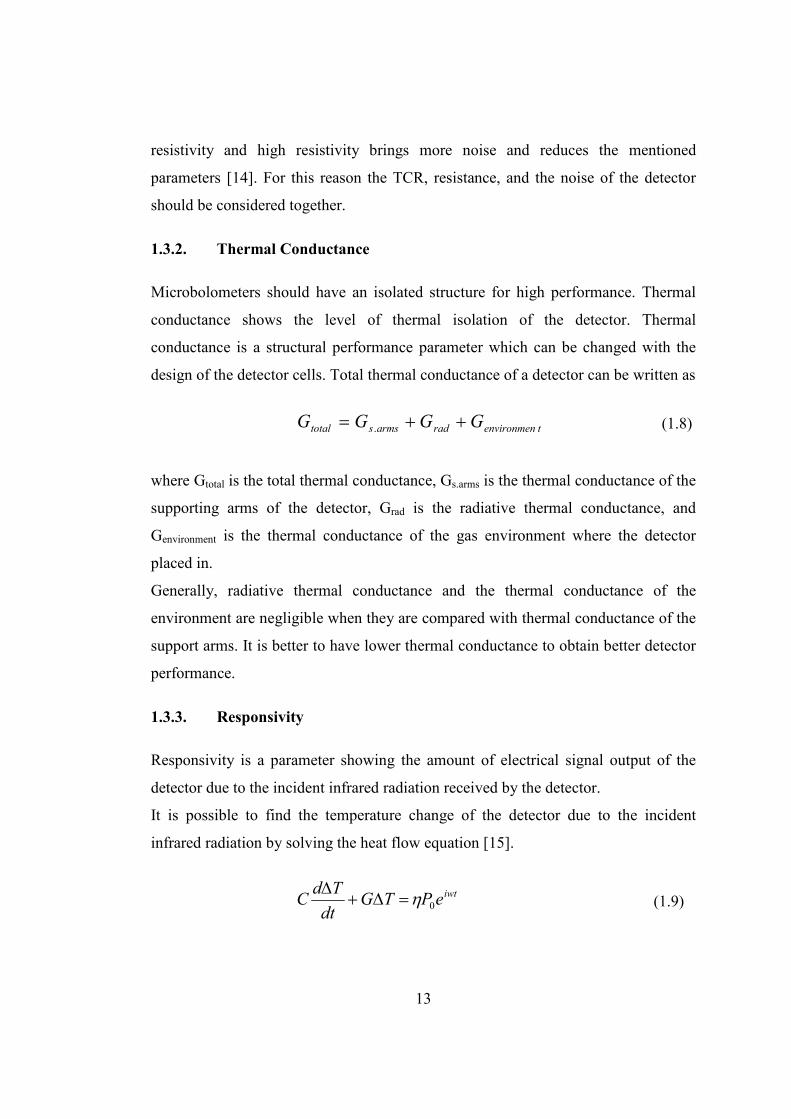
1.3.2. Thermal Conductance ............................................................... 13
1.3.3. Responsivity .............................................................................. 13
1.3.4. Noise Equivalent Power (NEP)................................................. 15
1.3.5. Noise Equivalent Temperature Difference NETD .................... 16
1.3.6. Detectivity (D*) ........................................................................ 17
1.4. Microbolometer active materials ........................................................ 17
1.4.1. VOx as Microbolometer Absorbing Material ............................ 19
1.4.2. Vanadium Oxide Systems ......................................................... 20
1.5. Sol-Gel Method and Thin Film Coating ............................................. 22
1.5.1. Sol-gel Chemistry ..................................................................... 22
1.5.2. Thin Film Coating ..................................................................... 24
1.6. Organization of the Thesis.................................................................. 25
xii
2. SOL-GEL DEPOSITION OF VOx THIN FILMS ............................................ 27
2.1. VOx Sol-Gel Trials in the Literature .................................................. 27
2.1.1. Organic VOx trials ..................................................................... 27
2.1.2. Inorganic VOx trials .................................................................. 28
2.2. Solution Preparation and Thin Film Coating Procedures ................... 30
2.2.1. Solution Preparation Procedure ................................................ 30
2.2.1.1. Solid Material Preparation (Vanadium) .......................... 30
2.2.1.2. Coating Solution Preparation........................................... 35
2.2.2. Thin Film Coating Procedure .................................................... 39
2.2.2.1. Preparation of the Substrates ........................................... 39
2.2.2.2. Spin Coating .................................................................... 43
2.3. Solution Preparation and Thin Film Coating Results ......................... 45
2.3.1. Solution ..................................................................................... 45
2.3.1.1. Solid Material Preparation Trials .................................... 46
2.3.1.2. Coating Solution Preparation Trials ................................ 50
2.3.2. Spin Coating .............................................................................. 52
3. ANNEALING OF VOx THIN FILMS .............................................................. 55
3.1. Annealing Trials of VOx Films in the Literature ................................ 55
3.2. Annealing Procedure .......................................................................... 59
3.3. Annealing Results ............................................................................... 62
3.3.1. Annealing Time Dependency.................................................... 67
3.3.2. H2 Concentration Dependency .................................................. 71
3.3.3. Reproducibility (Annealing) ..................................................... 75
4. PERFORMANCE OF SOL-GEL DEPOSITED VOx THIN FILMS ............... 76
4.1. Measurement Methods ....................................................................... 76
4.1.1. Sheet Resistance Measurement Method ................................... 76
4.1.2. TCR and Noise Measurements ................................................. 78
4.2. Results of The Measurements ............................................................ 83
4.2.1. Sheet Resistance Results ........................................................... 83
4.2.2. TCR and Noise Measurement Results ...................................... 85
5. CONCLUSIONS ............................................................................................... 95
REFERENCES ........................................................................................................... 98
xiii
LIST OF TABLES
TABLES
Table 1.1 – Infrared Radiation Regions ....................................................................... 3
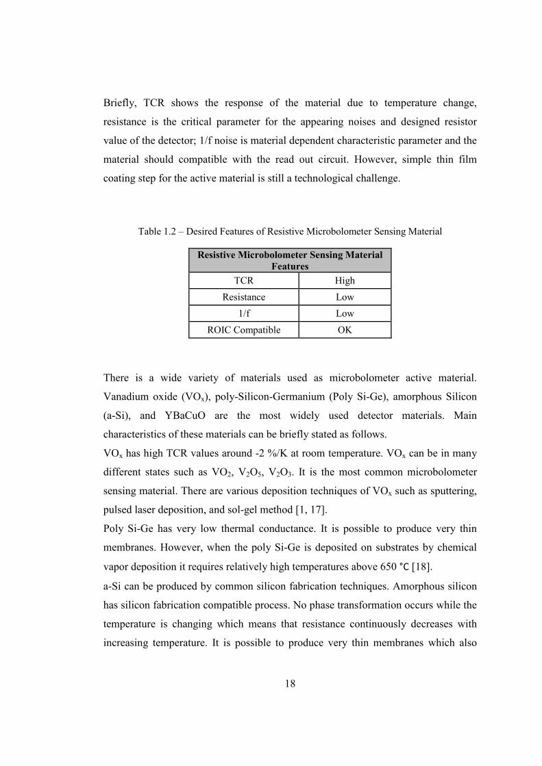
Table 1.2 – Desired Features of Resistive Microbolometer Sensing Material .......... 18
Table 1.3 – Metal – insulator transition temperatures of different vanadium oxide phases. ................................................................................................... 21
Table 2.1 – Dissolving vanadium powder in hydrogen peroxide trials and mixing ratios. Every dissolving trial has a color code (light grey, dark grey and grey). Light Grey: less dense solutions, Dark Grey: vanadium powder was remains, Grey: desired solution. .................................................... 46
Table 2.2 – Coating solution preparation trials with solid material and DI water. The trials are colored in respect to the successfulness of the trials. Light grey colored trials have lower densities, grey colored trials are successful enough for spin coating and dark grey colored trials are denser and have lots of unsolved solid particles. .................................. 51
Table 2.3 – Measured viscosities of the coating solutions ......................................... 52
Table 2.4 – Spin coating trials.................................................................................... 53
Table 2.5 – Spin speed and thickness relation of the thin films ................................. 54
Table 3.1 – Annealing conditions to reduce V2O5 to lower oxygen states. ................ 56
Table 3.2 – Various annealing trials were tried to find the appropriate annealing procedure. ............................................................................................. 59
Table 3.3 – Reducing V2O5 to VOx annealing trials. ................................................. 62
Table 3.4 – The annealing plan for the reduction process. ........................................ 66
Table 4.1 – The sheet resistance values and the VOx structure of the samples. Light grey colored samples are V2O5 structured and dark grey colored samples are reduced VOx structured. .................................................... 83
Table 4.2 – The sheet resistances of the films. The XRD patterns of these films were presented in previous sections. ............................................................. 84
Table 4.3 – RMS Noise Values of Sample-1 ............................................................. 90

xiv
Table 4.4 – RMS Noise Values of Sample-2 ............................................................. 91
xv
LIST OF FIGURES
FIGURES
Figure 1.1– Radiation mechanisms; when the incident radiation reaches the material, it can be absorbed, transmitted or reflected. The emitted ration is the consequence of the internal motion of the material. ................................. 4
Figure 1.2 – Plot of atmospheric transmittance in part of the infrared region [6] ....... 5
Figure 1.3 – Band gap structure of a semiconductor (a) at low temperature (b) at room temperature, Ev refers valance band, Ec is conduction band and Eg is the band gap of the semiconductor. ....................................................... 6
Figure 1.4 – Thermocouple structure, two materials with different seebeck coefficient. ................................................................................................ 7
Figure 1.5 – Basic structure of a thermopile, N thermocouples are connected to obtain higher voltage difference between two different materials. ........... 8
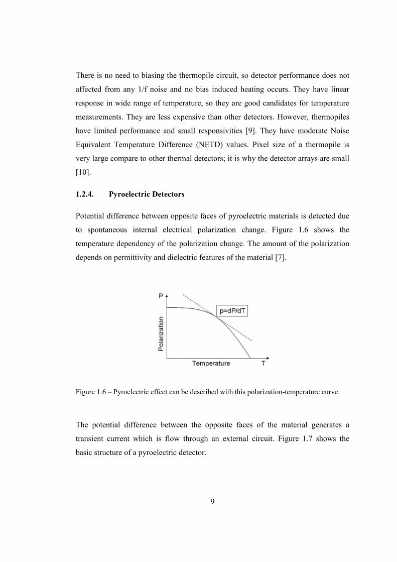
Figure 1.6 – Pyroelectric effect can be described with this polarization-temperature curve. ......................................................................................................... 9
Figure 1.7 – Basic structure of a pyroelectric detector which has pyroelectric material between two electrodes. ............................................................ 10
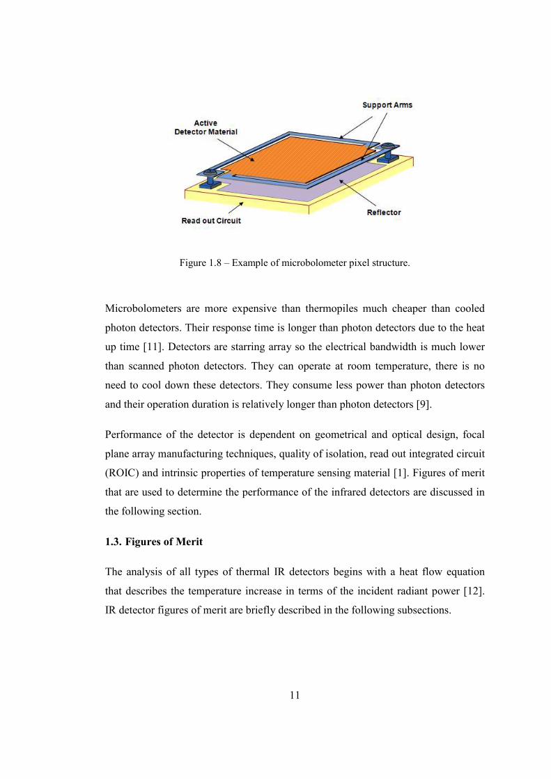
Figure 1.8 – Example of microbolometer pixel structure .......................................... 11
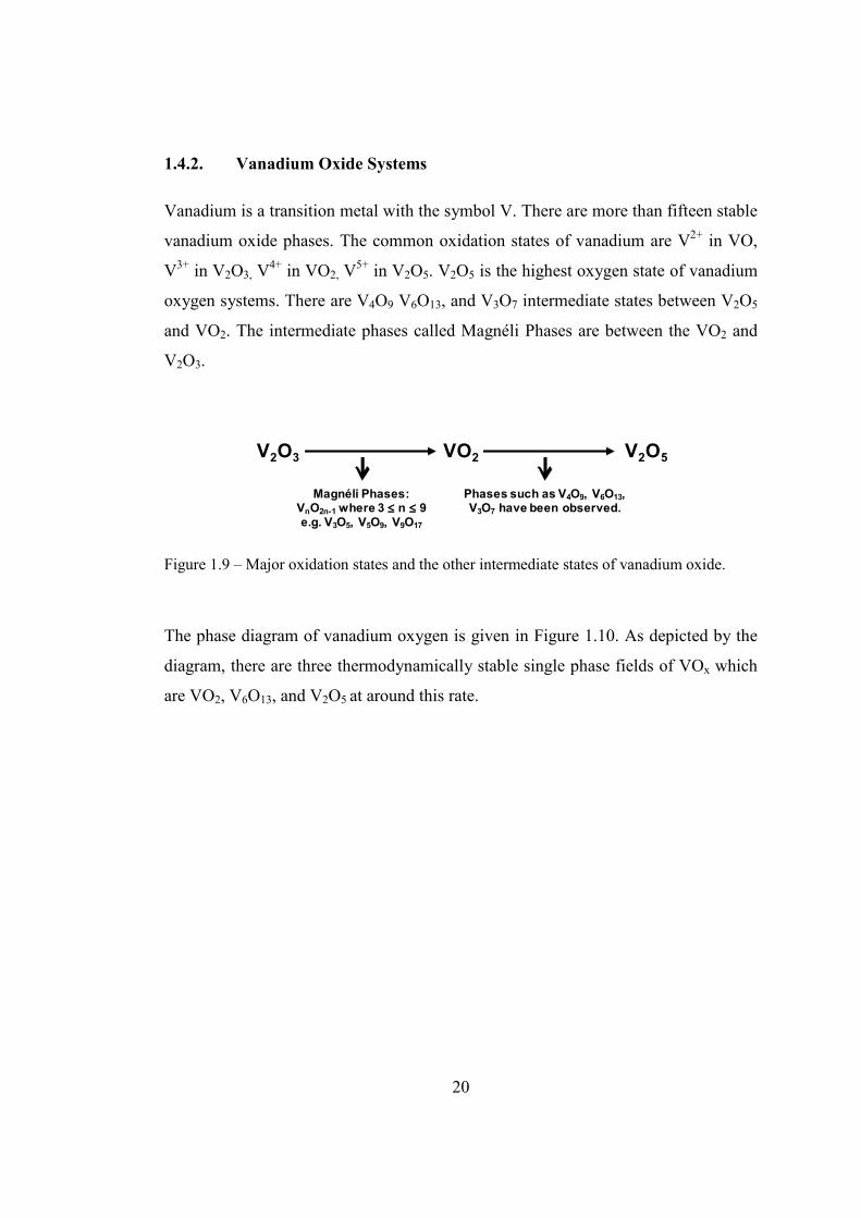
Figure 1.9 – Major oxidation states and the other intermediate states of vanadium oxide. ....................................................................................................... 20
Figure 1.10 – Phase diagram for the vanadium oxygen system [3] ........................... 21
Figure 1.11 – Olation (left) and oxolation (right) condensation mechanisms ........... 23
Figure 1.12 – (a) deposition (b) spin up (c) spin off phase-1 (d) spin off phase-2 (e) evaporation .............................................................................................. 24
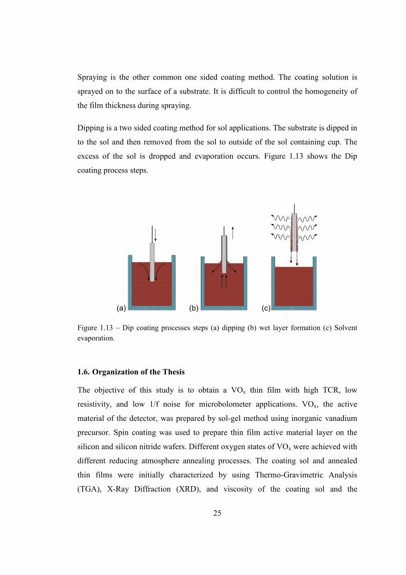
Figure 1.13 – Dip coating processes steps (a) dipping (b) wet layer formation (c) Solvent evaporation ................................................................................ 25
Figure 2.1 – The flow diagram of first step of the solution preparation. Appropriate amount of vanadium powder and hydrogen peroxide were mixed in ice cooled bath for 4-6 hours. ..................................................................... 31
xvi
Figure 2.2 – (a) Vanadium - hydrogen peroxide mixture in iced cooled bath (2 ºC)in the beginning of the dissolution process. (b) light red color mixture after a couple hours (4hours – 6 hours). ............................................... 32
Figure 2.3 – (a) The solution was in rest in ambient condition (at the beginning), (b) Oxygen release was reaching the peak point (c,d) Violent bubbling ... 33
Figure 2.4 – (a) Homogenous red sol at ambient temperature right after the reaction is stopped, (b) Dark brown sol with particles at the bottom (Flocculation). ....................................................................................... 33
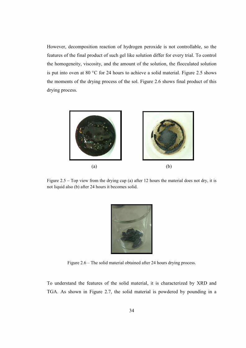
Figure 2.5 – Top view from the drying cup (a) after 12 hours the material does not dry, it is not liquid also (b) after 24 hours it becomes solid. ................ 34
Figure 2.6 – The solid material obtained after 24 hours drying process. ................... 34
Figure 2.7 – The solid material pounded in a mortar and powdered for characterization processes. .................................................................... 35
Figure 2.8 – The tip of the cracker was inside the solution. It sends pulsed ultrasonic waves. ................................................................................................... 36
Figure 2.9 – Preparation flow chart of the final coating solution. Solid material and DI water mixed and stirred. After ultrasonic processes flittering is applied to obtain the dark brown homogeneous coating solution. ....... 37
Figure 2.10 – Dark brown coating solution, considerably viscous and ready for spin coating. .................................................................................................. 38
Figure 2.11 – Brookfield DV-E Viscometer was used to measure the viscosity of the final coating solutions. .......................................................................... 38
Figure 2.12 –Two step cleaning applied to 2 x 2 cm Si wafer before spin coating process. ................................................................................................. 40
Figure 2.13 – Flow diagram of the base/acid cleaning, substrates cleaned in base and acid and then rinsed with water. They were dried in an oven to be ready for the second step cleaning. ................................................................. 41
Figure 2.14 – Two square wafers are in the ultrasonic bath while in the cleaning process. ................................................................................................. 41
Figure 2.15 – Acetone, ethanol, DI water cleaning flow. The substrates were ultrasonically cleaned with acetone and ethanol and than rinsed with DI water. They were dried in an oven to be ready for spin coating process. .............................................................................................................. 42
Figure 2.16 – Programmable spin coater was used for thin film coating process. .... 43
xvii
Figure 2.17 – Before spin coating, enough amount of solution was put on to the surface of wafer to cover it. .................................................................. 44
Figure 2.18 – Veeco Dektak 8 Surface Profiler is used for thickness measurement of the spin coated thin films. ..................................................................... 45
Figure 2.19 – Major solution preparation steps, vanadium powder dissolved in hydrogen peroxide, the solution was dried to obtain solid material and the solid material solved in DI water for final coating solution. .......... 45
Figure 2.20 – XRD pattern of solid material (blue peaks are V2O5.1.6H2O), The
major peaks are at (2θ = 8°, 22°, 31° and 39°) ..................................... 47
Figure 2.21 – The TGA curve of not annealed sample in N2 environment between 25 °C and 550 °C. ...................................................................................... 48
Figure 2.22 – XRD Pattern of solid material powder annealed at 370 °C for 2 hours (blue peaks are V2O5) JCPDS card no: 41-1426 ................................... 49
Figure 2.23 – The TGA curve of V2O5 sample in N2 environment between 25 °C and 550 °C. .................................................................................................. 50
Figure 2.24 – (a) Not coated, clean SiNx substrate, (b) totally coated substrate ........ 52
Figure 3.1 – XRD spectra of VOx film reduced from vacuum heating of V2O5 film [41] ........................................................................................................ 57
Figure 3.2 – V2O5 to VO2 reduction steps.................................................................. 58
Figure 3.3 – RTA tube furnace which allows annealing under vacuum and hydrogen environments ......................................................................................... 60
Figure 3.4 – Annealing flow chart; drying was applied after spin coating, two step annealing was used to reduction of V2O5 to VOx. ................................ 61
Figure 3.5 – The sample was annealed under air for 2 hours at 400 °C, there are two main peaks which are matched with (001) and (002) planes of V2O5 (JCPDS 41-1426), “S” peak comes from the substrate ........................ 63
Figure 3.6 – The sample was annealed under nitrogen for 5 hours at 400 °C, there are two main peaks which are matched with (001) and (002) planes of V2O5 (JCPDS 41-1426), “S” peak comes from the substrate ............... 64
Figure 3.7 – The sample was annealed firstly under air for 2 hours at 400 °C and than under nitrogen for 5 hours at 400 °C, there are two main peaks which are matched with (001) and (002) planes of V2O5 (JCPDS 41-1426) ..................................................................................................... 64
xviii
Figure 3.8 – The XRD pattern of the film annealed firstly under H2/N2 environment for 2 hours and then N2 environment for 2 hours. V2O5, VO2 and V6O13 peaks are observed. ............................................................................... 65
Figure 3.9 – XRD patterns of the films were annealed under 10 % H2/N2 environment at 410°C for (a) 2 hours, (b) 2.5 hours and then both films were annealed in N2 environment at 410 °C for 1 hour. ....................... 67
Figure 3.10 – XRD patterns of the films were annealed under 20 % H2/N2 environment at 410 °C for (c) 1.5 hours, (d) 2 hours, (e) 2.5 hours and than all films were annealed in N2 environment at 410 °C for 1 hour. . 68
Figure 3.11 – XRD patterns of the films were annealed under 30 % H2/N2 environment at 410 °C for (f) 1.5 hours, (g) 2 hours, (h) 2.5 hours and then all films were annealed in N2 environment at 410 °C for 1 hour. 70
Figure 3.12 – XRD patterns of the films were annealed under 40 % H2/N2 environment at 410 °C for (f) 1.5 hours, (g) 2hours, (h) 2.5 hours and then all films were annealed in N2 environment at 410 °C for 1 hour. . 71
Figure 3.13 – XRD patterns of the films were annealed for 1.5 hours at 410 °C in (c) 20 %, (f) 30 %, (j) 40 % hydrogen concentration of annealing environment and then all films were annealed in N2 environment at 410 °C for 1 hour. ........................................................................................ 72
Figure 3.14 – XRD patterns of the films were annealed for 2 hours at 410 °C in (a) 10 %, (d) 20 %, (g) 30 % hydrogen concentration of annealing environment and then all films were annealed in N2 environment at 410 °C for 1 hour. ........................................................................................ 73
Figure 3.15 – XRD patterns of the films were annealed for 2.5 hours at 410 °C in (a) 10 %, (d) 20 %, (g) 30 % hydrogen concentration of annealing environment and then all films were annealed in N2 environment at 410 °C for 1 hour. ........................................................................................ 74
Figure 3.16 – Three samples were annealed under 20 % hydrogen concentration for 2 hours at 410 °C .................................................................................. 75
Figure 4.1 – QuadPro Four point probe measurement tool was used to measure the sheet resistances of VOx thin films. ...................................................... 77
Figure 4.2 – Four point probe measurement of semiconductor sheet resistance [53] 77
Figure 4.3 – QuadPro Four Point Probe Head ........................................................... 78
Figure 4.4 – Electrode wafer (a) finger resist, (b) planar resist ................................. 79
xix
Figure 4.5 – (a) Spin coater (METU-MEMS clean room) (b) the wafer was put on to the chuck of the spin coater (c) the solution was put on the electrode wafer. .................................................................................................... 79
Figure 4.6 – (a) right after the VOx solution coated on the electrode wafer (b) the wafer was annealed under 20 % H2N2 environment at 410 °C for 2.5 hours (c) same wafer annealed under N2 environment at 410 °C for 1 hour. ................................................................................................... 80
Figure 4.7 – EV Group EVG 620 lithography and aligner located at METU-MEMS clean room. ............................................................................................ 81
Figure 4.8 – Common steps of a lithography process [54] ........................................ 82
Figure 4.9 – Resistance vs Temperature trend of Sample-1. ..................................... 86
Figure 4.10 – TCR trend of Sample-1 ........................................................................ 87
Figure 4.11 – Resistance vs Temperature trend of Sample-2. ................................... 88
Figure 4.12 – TCR trend of Sample-2 ........................................................................ 89
Figure 4.13 – Noise Power Spectral Density vs Frequency of Sample-1, 50 kΩ resistance under 20 µA bias. ................................................................. 90
Figure 4.14 – Noise Power Spectral Density vs Frequency of Sample-1, 250 kΩ resistance under 10 µA bias. ................................................................. 91
Figure 4.15 – Noise Power Spectral Density and Frequency slope of Sample-1. ..... 92
Figure 4.16 – Noise Power Spectral Density and Frequency slope of Sample-2. ..... 93
1
CHAPTER 1
INTRODUCTION
Infrared (IR) imaging technologies have been developed rapidly in the last three
decades. High performance IR detectors are now real, and they are getting better
each day. However, their power consumption and cost effectiveness are major
concerns for the future developments. Imaging and detection in the long wave
infrared (LWIR) region, between 8 µm – 14 µm, can be achieved with photon
detectors which uses direct photon excitation of electron hole pairs in narrow band
gap. Photon detectors need cryogenic cooling around 77 K for high intrinsic carrier
concentration. Cryogenic cooled FPAs (Focal Plane Arrays) reaches very high
performances, but they are not applicable for many applications because of their
heaviness and their high costs. On the other hand, uncooled (room temperature) IR
detectors such as microbolometers have become the most preferred choice in most of
the range of applications with their low cost. The most common applications of
microbolometers are thermography, night vision for military, commercial, and
automotive applications, mine detection, reconnaissance, surveillance, fire fighting,
and medical imaging [1].
The working principle of microbolometer is based on the thermoresistance effect.
Microbolometers absorb electromagnetic radiation which produces a temperature
increase. Most commonly, this temperature change is measured by a resistance
change. Microbolometer has an absorber area which absorbs incoming photons,
resulting the temperature and also resistance change of the detector. This change is
read by an electronic circuit.
2
The most common microbolometer detector active materials are VOx, amorphous
silicon, polycrystalline silicon – germanium, and yttrium barium copper oxide
(YBCO). VOx is a better bolometer material because of its combination of high
TCR, good IR absorbtion characteristics and low noise [2]. It is possible to achieve
high TCR values in the range of -2 %/K and -3 %/K by using VOx active layer at
room temperature [1].
There are many methods to prepare VOx thin films, such as sputtering, pulsed laser
deposition, and sol-gel method. Sol-gel method is one step forward from the others
with its conspicuous features which are low cost, easiness of the process, and
suitability for large area deposition [3].
Sol-gel method is a wet-chemical synthesis technique that is used primarily for the
fabrication of gels, glasses, and ceramic powders starting from a chemical solution
(typically a metal oxide). The sols undergo hydrolysis and
condensation/polymerization reactions leading to gel networks of discrete particles
or network polymers. There are two types of precursors: metal alkoxides dissolved in
organic solvents (organic) or metal salts in aqueous solutions (inorganic) can be used
as starting materials. Inorganic aqueous solutions are highly preferred in industrial
applications because of high cost and high reactivity disadvantage of organic
precursors [4]. Considering the advantages of sol-gel method, this thesis presents the
vanadium oxide (VOx) thin films elaborated by sol-gel method for microbolometer
applications.
Following sections of Chapter 1 will provide an introduction about several topics.
Section 1.1 gives information about the infrared region in the electromagnetic
spectrum and the radiation mechanisms of the materials, while the Section 1.2 makes
an overview of the infrared detectors. Section 1.3 gives the brief information about
infrared detector figures of merit, and Section 1.4 discusses the microbolometer
active materials and VOx systems. Section 1.5 explains the sol-gel method and thin
film coating process of sol-gels. Finally, Section 1.6 summarizes the aim of the study
and the organization of the thesis.
3
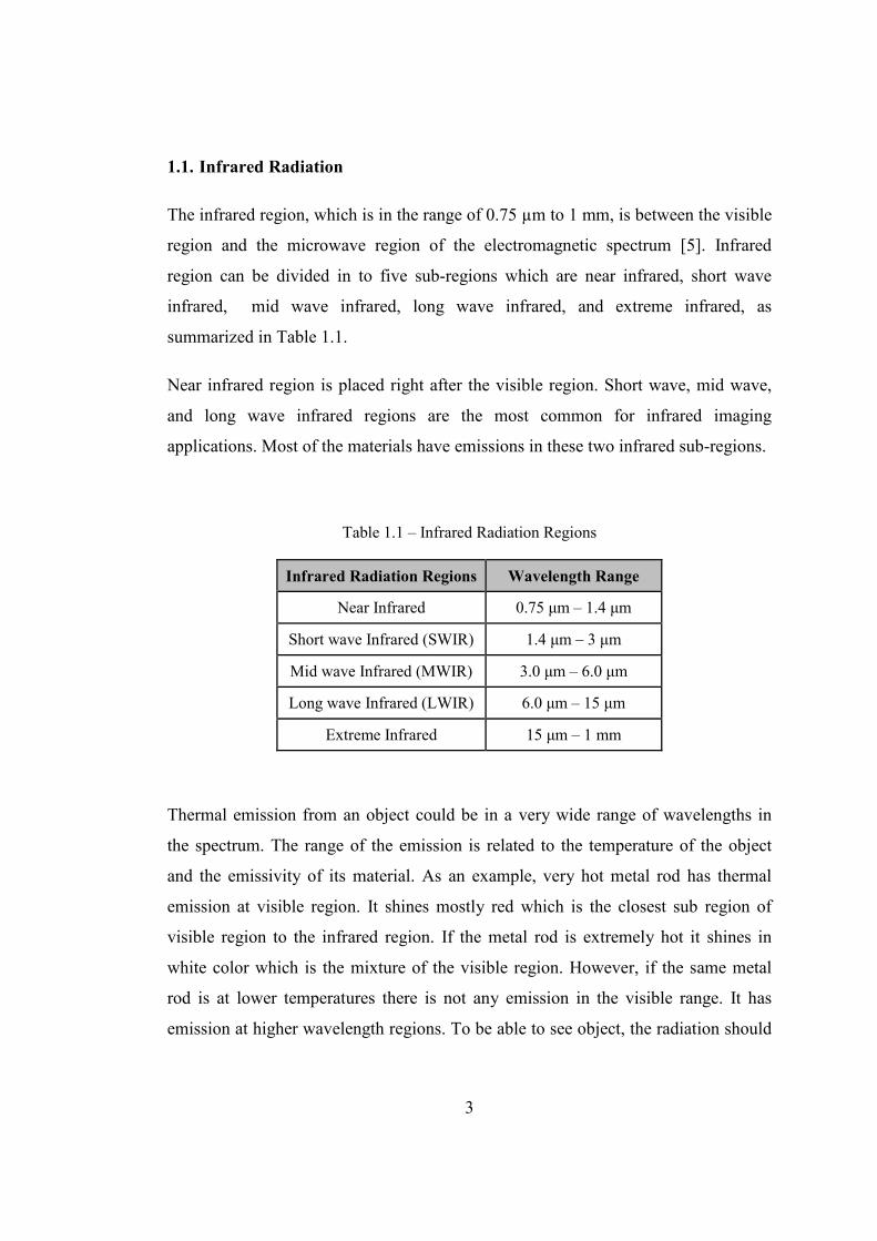
1.1. Infrared Radiation
The infrared region, which is in the range of 0.75 µm to 1 mm, is between the visible
region and the microwave region of the electromagnetic spectrum [5]. Infrared
region can be divided in to five sub-regions which are near infrared, short wave
infrared, mid wave infrared, long wave infrared, and extreme infrared, as
summarized in Table 1.1.
Near infrared region is placed right after the visible region. Short wave, mid wave,
and long wave infrared regions are the most common for infrared imaging
applications. Most of the materials have emissions in these two infrared sub-regions.
Table 1.1 – Infrared Radiation Regions
Infrared Radiation Regions Wavelength Range
Near Infrared 0.75 µm – 1.4 µm
Short wave Infrared (SWIR) 1.4 µm – 3 µm
Mid wave Infrared (MWIR) 3.0 µm – 6.0 µm
Long wave Infrared (LWIR) 6.0 µm – 15 µm
Extreme Infrared 15 µm – 1 mm
Thermal emission from an object could be in a very wide range of wavelengths in
the spectrum. The range of the emission is related to the temperature of the object
and the emissivity of its material. As an example, very hot metal rod has thermal
emission at visible region. It shines mostly red which is the closest sub region of
visible region to the infrared region. If the metal rod is extremely hot it shines in
white color which is the mixture of the visible region. However, if the same metal
rod is at lower temperatures there is not any emission in the visible range. It has
emission at higher wavelength regions. To be able to see object, the radiation should
4
be reflected or emitted from that object. As it was explained, the emission is related
to the temperature of the object.
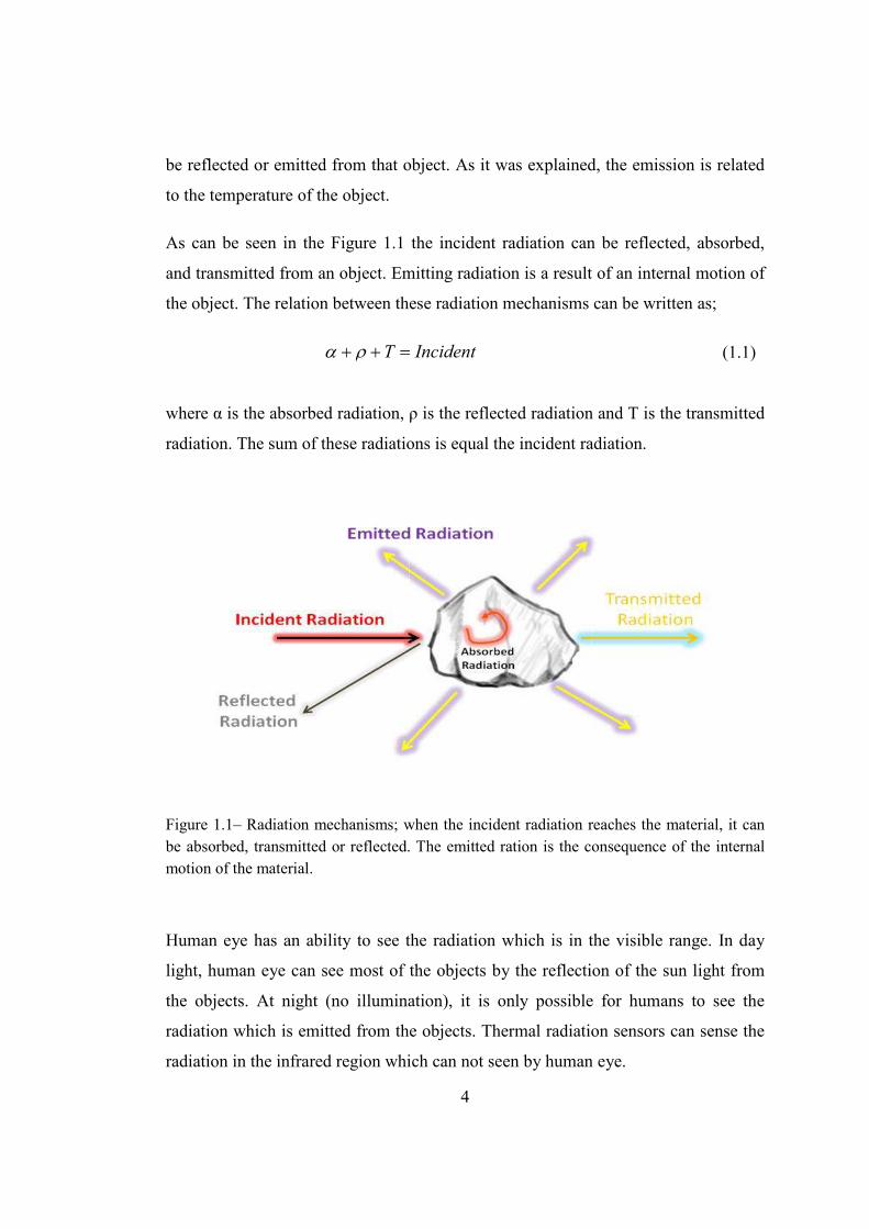
As can be seen in the Figure 1.1 the incident radiation can be reflected, absorbed,
and transmitted from an object. Emitting radiation is a result of an internal motion of
the object. The relation between these radiation mechanisms can be written as;
IncidentT =++ ρα (1.1)
where α is the absorbed radiation, ρ is the reflected radiation and T is the transmitted
radiation. The sum of these radiations is equal the incident radiation.
Figure 1.1– Radiation mechanisms; when the incident radiation reaches the material, it can
be absorbed, transmitted or reflected. The emitted ration is the consequence of the internal
motion of the material.
Human eye has an ability to see the radiation which is in the visible range. In day
light, human eye can see most of the objects by the reflection of the sun light from
the objects. At night (no illumination), it is only possible for humans to see the
radiation which is emitted from the objects. Thermal radiation sensors can sense the
radiation in the infrared region which can not seen by human eye.
5
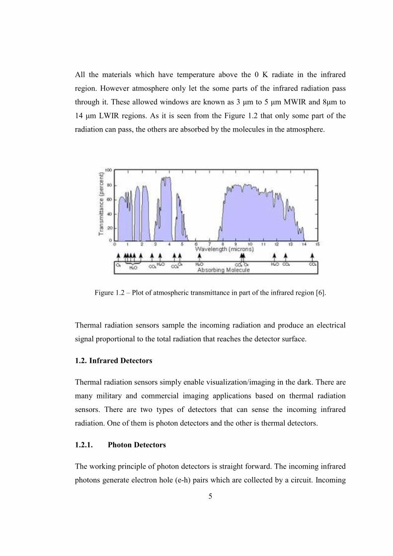
All the materials which have temperature above the 0 K radiate in the infrared
region. However atmosphere only let the some parts of the infrared radiation pass
through it. These allowed windows are known as 3 µm to 5 µm MWIR and 8µm to
14 µm LWIR regions. As it is seen from the Figure 1.2 that only some part of the
radiation can pass, the others are absorbed by the molecules in the atmosphere.
Figure 1.2 – Plot of atmospheric transmittance in part of the infrared region [6].
Thermal radiation sensors sample the incoming radiation and produce an electrical
signal proportional to the total radiation that reaches the detector surface.
1.2. Infrared Detectors
Thermal radiation sensors simply enable visualization/imaging in the dark. There are
many military and commercial imaging applications based on thermal radiation
sensors. There are two types of detectors that can sense the incoming infrared
radiation. One of them is photon detectors and the other is thermal detectors.
1.2.1. Photon Detectors
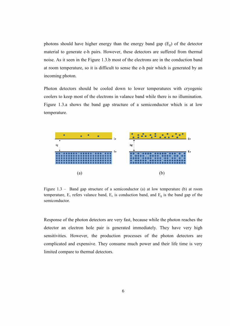
The working principle of photon detectors is straight forward. The incoming infrared
photons generate electron hole (e-h) pairs which are collected by a circuit. Incoming
6
photons should have higher energy than the energy band gap (Eg) of the detector
material to generate e-h pairs. However, these detectors are suffered from thermal
noise. As it seen in the Figure 1.3.b most of the electrons are in the conduction band
at room temperature, so it is difficult to sense the e-h pair which is generated by an
incoming photon.
Photon detectors should be cooled down to lower temperatures with cryogenic
coolers to keep most of the electrons in valance band while there is no illumination.
Figure 1.3.a shows the band gap structure of a semiconductor which is at low
temperature.
(a) (b)
Figure 1.3 – Band gap structure of a semiconductor (a) at low temperature (b) at room
temperature, Ev refers valance band, Ec is conduction band, and Eg is the band gap of the
semiconductor.
Response of the photon detectors are very fast, because while the photon reaches the
detector an electron hole pair is generated immediately. They have very high
sensitivities. However, the production processes of the photon detectors are
complicated and expensive. They consume much power and their life time is very
limited compare to thermal detectors.
7
1.2.2. Thermal Detectors
The other type of infrared detectors is thermal detectors which absorbs the incoming
infrared radiation and respond with a change of an electrical property such as
resistance, capacitance or voltage. This electrical change is measured by an
electronic read out circuit. Response time of the thermal detectors is longer than the
photon detectors because they need a heat up time after the incoming radiation is
absorbed. Thermal detectors work at room temperature. Their production is easier
than photon detectors. They are less expensive; consume less power and smaller in
size compare to photon detectors. There are three most common thermal detectors;
thermoelectric detectors (thermopiles), pyroelectric detectors and resistive
microbolometers.
1.2.3. Thermoelectric Detectors (Thermopiles)
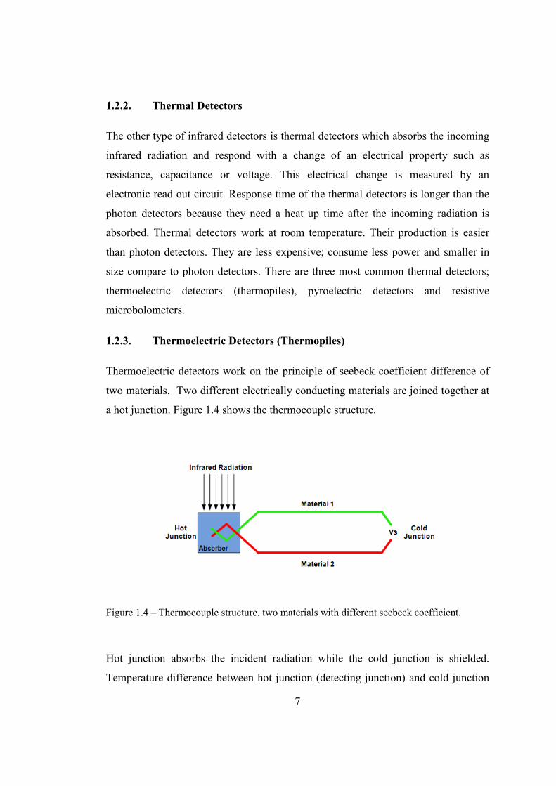
Thermoelectric detectors work on the principle of seebeck coefficient difference of
two materials. Two different electrically conducting materials are joined together at
a hot junction. Figure 1.4 shows the thermocouple structure.
Figure 1.4 – Thermocouple structure, two materials with different seebeck coefficient.
Hot junction absorbs the incident radiation while the cold junction is shielded.
Temperature difference between hot junction (detecting junction) and cold junction
8
(shielded junction) create a voltage difference between two materials [7]. This
structure is called as thermocouple. Obtained voltage is directly related to
temperature difference between the junctions and the electrical conductivity of the
materials.
Obtained voltage can be written as
( ) TSSVs ∆−= 21 (1.2)
where Vs is the thermoelectric signal voltage, S1 and S2 are the seebeck coefficients
of the materials and ∆T is the temperature difference between hot junction and the
cold junction.
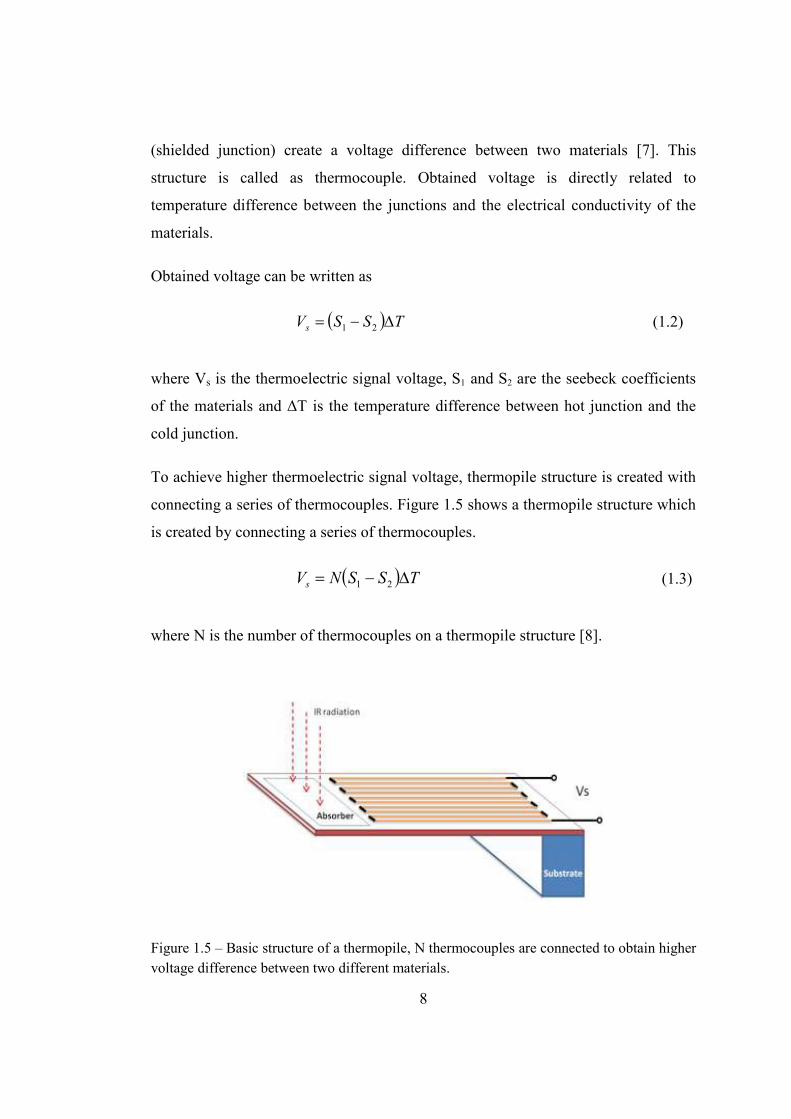
To achieve higher thermoelectric signal voltage, thermopile structure is created with
connecting a series of thermocouples. Figure 1.5 shows a thermopile structure which
is created by connecting a series of thermocouples.
( ) TSSNVs ∆−= 21 (1.3)
where N is the number of thermocouples on a thermopile structure [8].
Figure 1.5 – Basic structure of a thermopile, N thermocouples are connected to obtain higher
voltage difference between two different materials.
9
There is no need to biasing the thermopile circuit, so detector performance does not
affected from any 1/f noise and no bias induced heating occurs. They have linear
response in wide range of temperature, so they are good candidates for temperature
measurements. They are less expensive than other detectors. However, thermopiles
have limited performance and small responsivities [9]. They have moderate Noise
Equivalent Temperature Difference (NETD) values. Pixel size of a thermopile is
very large compare to other thermal detectors; it is why the detector arrays are small
[10].
1.2.4. Pyroelectric Detectors
Potential difference between opposite faces of pyroelectric materials is detected due
to spontaneous internal electrical polarization change. Figure 1.6 shows the
temperature dependency of the polarization change. The amount of the polarization
depends on permittivity and dielectric features of the material [7].
Figure 1.6 – Pyroelectric effect can be described with this polarization-temperature curve.
The potential difference between the opposite faces of the material generates a
transient current which is flow through an external circuit. Figure 1.7 shows the
basic structure of a pyroelectric detector.
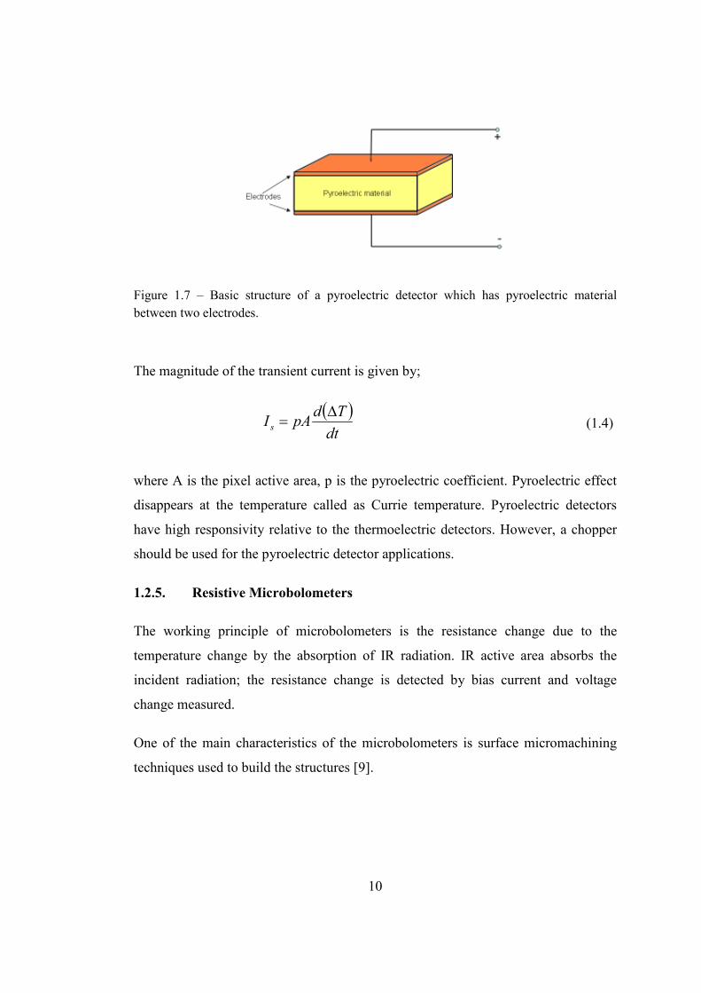
10
Figure 1.7 – Basic structure of a pyroelectric detector which has pyroelectric material
between two electrodes.
The magnitude of the transient current is given by;
( )dt
TdpAI s
∆= (1.4)
where A is the pixel active area, p is the pyroelectric coefficient. Pyroelectric effect
disappears at the temperature called as Currie temperature. Pyroelectric detectors
have high responsivity relative to the thermoelectric detectors. However, a chopper
should be used for the pyroelectric detector applications.
1.2.5. Resistive Microbolometers
The working principle of microbolometers is the resistance change due to the
temperature change by the absorption of IR radiation. IR active area absorbs the
incident radiation; the resistance change is detected by bias current and voltage
change measured.
One of the main characteristics of the microbolometers is surface micromachining
techniques used to build the structures [9].
11
Figure 1.8 – Example of microbolometer pixel structure.
Microbolometers are more expensive than thermopiles much cheaper than cooled
photon detectors. Their response time is longer than photon detectors due to the heat
up time [11]. Detectors are starring array so the electrical bandwidth is much lower
than scanned photon detectors. They can operate at room temperature, there is no
need to cool down these detectors. They consume less power than photon detectors
and their operation duration is relatively longer than photon detectors [9].
Performance of the detector is dependent on geometrical and optical design, focal
plane array manufacturing techniques, quality of isolation, read out integrated circuit
(ROIC) and intrinsic properties of temperature sensing material [1]. Figures of merit
that are used to determine the performance of the infrared detectors are discussed in
the following section.
1.3. Figures of Merit
The analysis of all types of thermal IR detectors begins with a heat flow equation
that describes the temperature increase in terms of the incident radiant power [12].
IR detector figures of merit are briefly described in the following subsections.
12
1.3.1. Temperature Sensitivity
Temperature sensitivity is a parameter that describes the temperature dependency of
uncooled detectors. For resistive type microbolometers it is the temperature
dependence of the resistance. The resistance of the detector change with the increase
or decrease of the temperature. This dependence can be described as temperature
coefficient of resistance (TCR).
dT
dR
R
1=α (1.5)
where α is the TCR of the detector, R is the resistance at the temperature T. The
TCR is a property of the active material. The active material can be metal or
semiconductor. If the material is metal the TCR is positive, and if the material is
semiconductor the TCR is negative.
The free carrier concentration of the metals does not change so much with the
change of the temperature. However, the mobility of the free carriers is reduced by
the temperature change. The resistance of the thin film can be written as [13]:
( ) ( )( )ss TTTRTR −+= α1)( (1.6)
where R(T) is the resistance dependent to temperature T, Ts is room temperature, α is
TCR.
The mobile charge carriers of the semiconductors are increased with increasing
temperature. Furthermore, the mobility of the carriers are increased with increasing
temperature. The resistance of semiconductor thin films can be expressed as [13]
( )TkETR bg 2exp)( ∝ 22.,. TkERdTdRei bg−==α (1.7)
where Eg is the band gap of the semiconductor, kb is the Boltzman’s Constant.
Semiconductors such as VOx thin films give more TCR than most metal thin films.
Parameters that will be discussed in the following sections such as responsivity and
detectivity are increased with the increase in TCR. However, high TCR means high
13
resistivity and high resistivity brings more noise and reduces the mentioned
parameters [14]. For this reason the TCR, resistance, and the noise of the detector
should be considered together.
1.3.2. Thermal Conductance
Microbolometers should have an isolated structure for high performance. Thermal
conductance shows the level of thermal isolation of the detector. Thermal
conductance is a structural performance parameter which can be changed with the
design of the detector cells. Total thermal conductance of a detector can be written as
tenvironmenradarmsstotal GGGG ++= . (1.8)
where Gtotal is the total thermal conductance, Gs.arms is the thermal conductance of the
supporting arms of the detector, Grad is the radiative thermal conductance, and
Genvironment is the thermal conductance of the gas environment where the detector
placed in.
Generally, radiative thermal conductance and the thermal conductance of the
environment are negligible when they are compared with thermal conductance of the
support arms. It is better to have lower thermal conductance to obtain better detector
performance.
1.3.3. Responsivity
Responsivity is a parameter showing the amount of electrical signal output of the
detector due to the incident infrared radiation received by the detector.
It is possible to find the temperature change of the detector due to the incident
infrared radiation by solving the heat flow equation [15].
iwtePTGdt
TdC 0η=∆+
∆ (1.9)
14
where C is the heat capacity of the detector material, G is thermal conductance,
P0eiwt is the incident infrared radiation power, w is the frequency of radiation power,
and η is the absorption coefficient .
222
0
CwG
PT
+=∆
η (1.10)
Smaller C and G are required to have larger ∆T. The ratio of thermal capacitance and
thermal conductance can be expressed as thermal time constant. ∆T can be written in
terms of thermal time constant as follows.
22
0
1 thwG
PT
τ
η
+=∆ (1.11)
Output of detector can be expressed in terms of voltage or current due to the read out
design. The change of the output due to the temperature change can be written as
following equations.
TRIRIV biasbias ∆=∆=∆ α (1.12)
TR
V
TRR
V
R
VI biasbiasbias ∆−≈
∆−−=∆ α
α (1.13)
where Ibias is the bias current of the detector, R is the detector resistance, α is the
TCR of the detector and if the detector is biased with voltage, Vbias is the bias voltage
of the detector, ∆T is the temperature change.
The resposivities for the voltage biased and current biased detectors are expressed as
[16].
( ) 21221 th
biasv
wG
RIR
τ
ηα
+=
(1.14)
( ) 21221 th
biasi
wRG
VR
τ
αη
+= (1.15)
15
Responsivity is proportional to TCR and inversely proportional to thermal
conductance. The detector material and the isolation of the detector are the primary
focus for responsivity of the detector.
1.3.4. Noise Equivalent Power (NEP)
The amount incident power required to produce a signal which is above the noise
level of the detector. The signal power should be higher than the noise level to
detection.
i
noise
v
noise
R
i
R
VNEP == (1.16)
where Rv and Ri are the responsivity and Vnoise and inoise are the total rms noise
voltage and current.
There are four major noise mechanisms in bolometer [8].
a) Johnson (Thermal) Noise
b) 1/f Noise
c) Temperature Fluctuation Noise
d) Background Fluctuation Noise
Johnson noise is the fluctuation due to the thermal motion of charge carriers in
resistive materials and occurs in the absence of electrical bias.
R
fkTi johnsonn
∆=
4,
, fkTRV johnsonn ∆= 4, (1.17)
where k is the Boltzman constant, T is the temperature in Kelvin, R is the resistance
of the detector, and ∆f is the bandwidth.
1/f noise is found in semiconductors. 1/f noise is a major problem at low level
frequencies and inversely proportional to square root of frequency.
f
nVV fn
2
/1, = (1.18)
16
where V is the bias voltage, n is the 1/f noise parameter, f is the frequency. 1/f noise
depends on the active bolometer material [12].
Temperature fluctuation noise is caused by the change of the detector temperature
due to the heat loss from detector to detector surroundings.
vtfn RkTG
Vη
4, =
(1.19)
where G is the thermal conductance, η is the absorption coefficient, and Rv is the
responsivity of the detector.
Background fluctuation noise is caused by the random changes of incoming radiation
power and the random changes of emitted power from the detector. It can be
expressed as.
( ) vbackgroundbolometerdbfn RTTkAV 55, 8 += ησ
(1.20)
where Ad is the detector area, η is the absorption coefficient, σ is the Stefan-
Boltzman constant, k is the Boltzman constant, Tbolometer and Tbacground are the
temperatures of bolometer, and the background, Rv is the responsivity of the
detector.
Total rms noise voltage written as,
2,
2,
2/1,
2,, bfntfnfnjhonsonntotaln VVVVV +++=
(1.21)
1.3.5. Noise Equivalent Temperature Difference NETD
NETD is an infrared imager performance parameter which has dependency not only
the detector but also the other parts of the imaging system such as optics.
( )21
24
λλτ −∆∆=
TPRA
VFNETD
vd
n
(1.22)
17
where, F is the focal ratio of the optics, τ is the transmittance of the optics,
(∆P/∆T)λ1-λ2 is the change in power per unit area radiated by scene at temperature T,
T is measured within the spectral range of λ1 to λ2.
1.3.6. Detectivity (D*)
Detectivity is a parameter that is needed for comparison of different detectors in
terms of performance. It is possible to compare different pixel size different scanning
rate imagers with detectivity.
v
n
DDR
V
fA
NEP
fAD
∆=
∆=*
(1.23)
where AD is the active detector area, ∆f is the bandwidth of the system, NEP is the
noise equivalent power of the detector, Rv is the voltage responsivity of the detector
and Vn is the total rms noise voltage.
TCR and 1/f noise are the microbolometer active material dependent performance
parameters. The choice of the active material directly effects the performance of the
detector. Microbolometer active materials will be briefly explained in the following
section.
1.4. Microbolometer active materials
Microbolometer active material has a crucial importance on the performance of the
infrared imaging devices. The active material determines the sensitivity of the
microbolometer. Active material features that resistance, TCR, and 1/f noise are the
most effecting parameters on the detector design. The read out compatibility of the
material is also a very important issue. There are various processing routes for
developing active material on the detector structure in the form of a thin film.
However, some techniques such as high temperature deposition are not compatible
with the ROIC of the detector. Contacts of the circuit can melt at high temperatures
during deposition of the sensing material.
18
Briefly, TCR shows the response of the material due to temperature change,
resistance is the critical parameter for the appearing noises and designed resistor
value of the detector; 1/f noise is material dependent characteristic parameter and the
material should compatible with the read out circuit. However, simple thin film
coating step for the active material is still a technological challenge.
Table 1.2 – Desired Features of Resistive Microbolometer Sensing Material
Resistive Microbolometer Sensing Material Features
TCR High
Resistance Low
1/f Low
ROIC Compatible OK
There is a wide variety of materials used as microbolometer active material.
Vanadium oxide (VOx), poly-Silicon-Germanium (Poly Si-Ge), amorphous Silicon
(a-Si), and YBaCuO are the most widely used detector materials. Main
characteristics of these materials can be briefly stated as follows.
VOx has high TCR values around -2 %/K at room temperature. VOx can be in many
different states such as VO2, V2O5, V2O3. It is the most common microbolometer
sensing material. There are various deposition techniques of VOx such as sputtering,
pulsed laser deposition, and sol-gel method [1, 17].
Poly Si-Ge has very low thermal conductance. It is possible to produce very thin
membranes. However, when the poly Si-Ge is deposited on substrates by chemical
vapor deposition it requires relatively high temperatures above 650 °C [18].
a-Si can be produced by common silicon fabrication techniques. Amorphous silicon
has silicon fabrication compatible process. No phase transformation occurs while the
temperature is changing which means that resistance continuously decreases with
increasing temperature. It is possible to produce very thin membranes which also
19
lower the thermal conductance. Amorphous silicon can be deposited at very low
temperatures [1].
YBCO can be deposited at room temperature. It is possible to achieve high TCR
values around 3 %/K – 4 %/K with this material. YBCO has low 1/f noise [1].
1.4.1. VOx as Microbolometer Active Material
VOx is a suitable bolometer active material because of its combination of high TCR,
good IR absorption characteristics, and low 1/f noise. It is possible to achieve high
TCR values in the range of -2 %/K and -3 %/K by using VOx active layer at room
temperature. VOx can be deposited by sputtering, pulsed laser deposition, and sol-gel
method.
The material used as the detector active material must provide significant changes in
resistance in response to temperature change. Using a material with low room
temperature resistance is also important. Lower resistance across the detecting
material mean less power will need to be used. Also, there is a relationship between
resistance and noise, the higher the resistance the higher the noise. Thus, for easier
detection and to satisfy the low noise requirement, resistance should be low [19].
Vanadium is a multivalent element and can be in different oxidation states. A variety
of vanadium oxide phases, V2O5, VO2, V2O3, and multiphase VxOy combinations
have been used as active material in microbolometer applications. The important
question is “which one of them or which combination of them gives the better
performance results as a microbolometer active material?”
VO2 has low resistance but undergoes a metal-insulator phase change near 67 ºC and
also has a low value of TCR. On the other hand, V2O5 offers high resistance and also
high TCR. Many phases of VOx exist although it seems that (x ≈ 2 – 2.3) VOx phases
have become the most popular for microbolometer applications [20, 21]. Brief
information about vanadium oxide systems will be given in the following section.
20
1.4.2. Vanadium Oxide Systems
Vanadium is a transition metal with the symbol V. There are more than fifteen stable
vanadium oxide phases. The common oxidation states of vanadium are V2+ in VO,
V3+ in V2O3, V4+ in VO2, V
5+ in V2O5. V2O5 is the highest oxygen state of vanadium
oxygen systems. There are V4O9 V6O13, and V3O7 intermediate states between V2O5
and VO2. The intermediate phases called Magnéli Phases are between the VO2 and
V2O3.
V2O3 VO2 V2O5
Magnéli Phases:VnO2n-1where 3 ≤≤≤≤ n ≤≤≤≤ 9e.g. V3O5, V5O9, V9O17
Phases such as V4O9, V6O13, V3O7 have been observed.
Figure 1.9 – Major oxidation states and the other intermediate states of vanadium oxide.
The phase diagram of vanadium oxygen is given in Figure 1.10. As depicted by the
diagram, there are three thermodynamically stable single phase fields of VOx which
are VO2, V6O13, and V2O5 at around this rate.
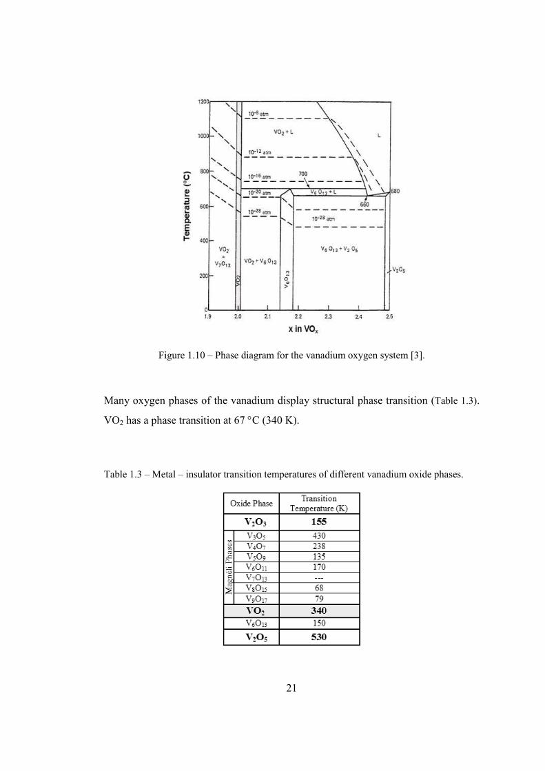
21
Figure 1.10 – Phase diagram for the vanadium oxygen system [3].
Many oxygen phases of the vanadium display structural phase transition (Table 1.3).
VO2 has a phase transition at 67 °C (340 K).
Table 1.3 – Metal – insulator transition temperatures of different vanadium oxide phases.
22
There is an interest on thin film processes of vanadium oxides in literature, due to
their widespread applications. There are many possible ways of thin film growth
method of vanadium oxide. Chemical vapor deposition (CVD), sputtering, pulsed
laser deposition, epitaxial growth and sol-gel method are the most common thin film
preparation of vanadium oxides. Sol-gel method and thin film coating will be
discussed in the following section.
1.5. Sol-Gel Method and Thin Film Coating
Beside the all other thin film preparation methods, sol-gel method has many
advantages. It does not require a high vacuum systems and the instrumentation is
much simpler. High purity stoichiometry can be achieved by low temperature
processes. Large substrates can easily be coated. It allows high deposition rates. The
starting materials are mixed on a molecular level; a very good chemical homogeneity
can be obtained [22].
1.5.1. Sol-gel Chemistry
Vanadium is a transition metal. A vanadium solution can be prepared from inorganic
(salts) or organic (metal-alkoxide) precursors. Alkoxides contain organic groups with
negatively charged oxygen atom which stabilizes the transition metal with its electro
negativity.
Organic sol-gel preparation method, involving use of alkoxide precursors and
organic solvents, has several advantages. Multi component films can be prepared by
mixing several metal-alkoxides in the same solvent. In addition, highly
homogeneous and products with molecular level purity can be obtained. However,
organic sol-gel processes are quite expensive than inorganic sol-gel processes and
highly reactive [4, 22, 23]. It is possible to say that inorganic sol-gel preparation
methods are more appropriate for industrial applications.
23
Inorganic precursors formed by dissolution of metal salts in aqueous, such as water.
Main mechanism of this dissolution is the charge transfer from water molecule to the
empty orbitals of the transition metal [24]. Hydrolysis of inorganic salt defined as:
[M(OH2)]z+ [M-OH](z-1)+ + H+ [M=O](z-2)+ + 2H+ (1.24)
where M is the transition metal. Different types of ligands can be formed in the
solution in respect to molar ratio of the hydrolysis.
• Aquo: M-(OH2)
• Hydroxo: M-OH
• Oxo: M=O
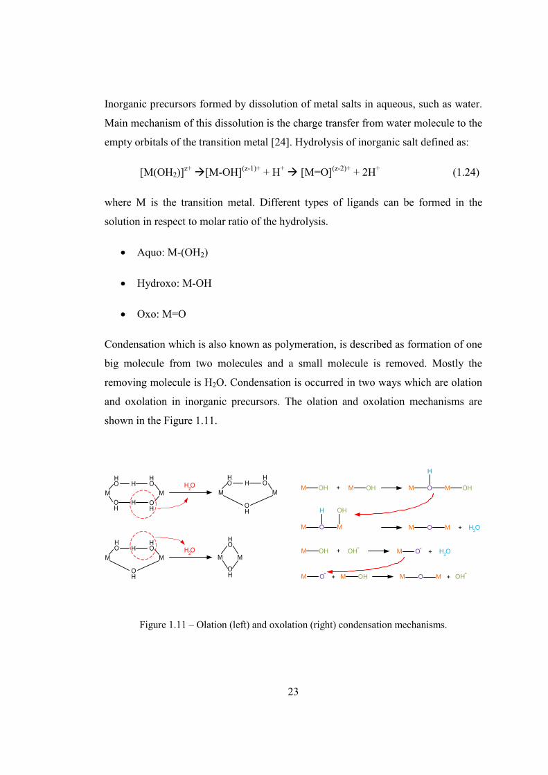
Condensation which is also known as polymeration, is described as formation of one
big molecule from two molecules and a small molecule is removed. Mostly the
removing molecule is H2O. Condensation is occurred in two ways which are olation
and oxolation in inorganic precursors. The olation and oxolation mechanisms are
shown in the Figure 1.11.
M
HO
M
H O2
HO
H
HHO
HO
M
HO
M
HHO
HO
M
HHO
M
HO
HO H O
2
HO
M M
HO
M OH + M OH M O M OH
H
M O M
OHH
M O M + H O2
M OH + M O-
+ H O2
M O-
+ M OH M O M +
OH-
OH-
Figure 1.11 – Olation (left) and oxolation (right) condensation mechanisms.
24
1.5.2. Thin Film Coating
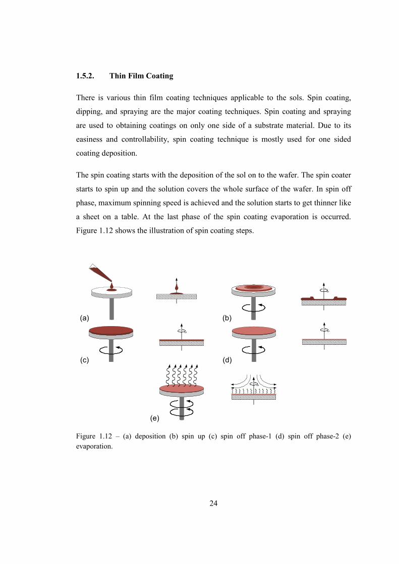
There is various thin film coating techniques applicable to the sols. Spin coating,
dipping, and spraying are the major coating techniques. Spin coating and spraying
are used to obtaining coatings on only one side of a substrate material. Due to its
easiness and controllability, spin coating technique is mostly used for one sided
coating deposition.
The spin coating starts with the deposition of the sol on to the wafer. The spin coater
starts to spin up and the solution covers the whole surface of the wafer. In spin off
phase, maximum spinning speed is achieved and the solution starts to get thinner like
a sheet on a table. At the last phase of the spin coating evaporation is occurred.
Figure 1.12 shows the illustration of spin coating steps.
(a) (b)
ω
(c)
ω
(d)
ω
(e)
ω
Figure 1.12 – (a) deposition (b) spin up (c) spin off phase-1 (d) spin off phase-2 (e)
evaporation.
25
Spraying is the other common one sided coating method. The coating solution is
sprayed on to the surface of a substrate. It is difficult to control the homogeneity of
the film thickness during spraying.
Dipping is a two sided coating method for sol applications. The substrate is dipped in
to the sol and then removed from the sol to outside of the sol containing cup. The
excess of the sol is dropped and evaporation occurs. Figure 1.13 shows the Dip
coating process steps.
(a) (b) (c)
Figure 1.13 – Dip coating processes steps (a) dipping (b) wet layer formation (c) Solvent
evaporation.
1.6. Organization of the Thesis
The objective of this study is to obtain a VOx thin film with high TCR, low
resistivity, and low 1/f noise for microbolometer applications. VOx, the active
material of the detector, was prepared by sol-gel method using inorganic vanadium
precursor. Spin coating was used to prepare thin film active material layer on the
silicon and silicon nitride wafers. Different oxygen states of VOx were achieved with
different reducing atmosphere annealing processes. The coating sol and annealed
thin films were initially characterized by using Thermo-Gravimetric Analysis
(TGA), X-Ray Diffraction (XRD), and viscosity of the coating sol and the
26
thicknesses of the thin films are also measured. The performance parameters of the
VOx active layer such as sheet resistance, TCR, and noise were measured to verify
the quality of the developed VOx layers for their use in microbolometers.
Chapter 2 gives literature review about sol-gel processing of vanadium oxide thin
films. It also highlights the experimental method, in regard to sol-gel procedure and
related results on the properties of VOx thin films.
Chapter 3 gives literature review about post coating annealing step for achieving
different states for VOx thin films. It also explains the annealing procedure, results of
successfully coated VOx thin films.
Chapter 4 gives the performance results of the successfully coated and annealed thin
films. The performed examinations include sheet resistance, TCR, and noise
measurements.
Finally, Chapter 5 summarizes the results of this thesis study.
27
CHAPTER 2
SOL-GEL DEPOSITION OF VOx THIN FILMS
There are many methods to prepare VOx thin films, such as reactive sputtering,
pulsed laser deposition, vacuum evaporation, and sol-gel techniques [25-29]. Low
cost, easiness of the process, low processing temperatures, suitability for large area
deposition and very pure products (crystallization, distillation, electrolysis) are the
most remarkable features of the sol-gel method [3, 4, 24, 30 , 31].
Due to these advantages of the sol-gel process, this method is chosen for this study
to prepare VOx microbolometer active material. Section 2.1 gives information about
the preparation trials of sol-gel vanadium oxide in the literature. Section 2.2
describes the sol preparation and thin film coating procedures. Section 2.3
summarizes the results of the sol preparations and thin film coating processes.
2.1. VOx Sol-Gel Trials in the Literature
There are various ways to prepare a metal oxide solution for thin film coating. As
mentioned earlier, organic and inorganic are two different sol-gel preparation
methods. Both of these methods can be used for VOx sol-gel preparation. Various
VOx sol-gel preparation methods have been described in the literature.
2.1.1. Organic VOx trials
The main route for organic VOx solution preparation method is described by Livage
[32] as follows:
28
Vanadium alkoxides VO(OR)3 (R=OPri, OAmt) were prepared by heating the
mixture ammonium vanadate and alcohol in an nonpolar solvent (C6H12). The
reaction can be written as
NH4VO3 + 3ROH VO(OR)3 + 2H2O + NH3 (2.1)
Reduced pressure was used to purify the resulting alcohol and it was dissolved in its
parent alcohol [33]. Due to the disadvantages which were mentioned in Section 1.5.1
of organic sol-gel method, inorganic sol-gel process of vanadium oxide was mostly
preferred instead of organic sol-gel process. Inorganic sol-gel trials will be examined
in the following section.
2.1.2. Inorganic VOx trials
Takahashi reported that it is possible to make polyvanadate by solving metallic
vanadium powder in hydrogen peroxide [25]. When metallic vanadium powder is
dissolved in hydrogen peroxide in ambient conditions, highly exothermic reaction
occur leading to violent conditions [25, 32]. Therefore, an external cooling device
such as ice cooled bath can be used to decrease the violence of the reaction [25].
However this type of external cooling hampers the dissolution of the metal in the
H2O2. In the absence of external cooling, vanadium can be dissolved in hydrogen
peroxide in 30 min, however external cooling expands this process to 5 h – 6 h. After
all the vanadium is dissolved in the H2O2 the solution is taken to rest to increase the
solution temperature to the ambient temperature. An exothermic and less violent
reaction was occurred while the temperature of the solution increases. Instead of
leaving the solution to rest, It is possible to heat the solution to higher temperatures
(close to ambient temperature ~ 50 °C) [25]. More rapid reaction is occurred if the
solution is heated.
Concentration of the hydrogen peroxide can also change the reaction characteristics.
If the concentration of the hydrogen peroxide is kept at lower levels (around 10 %),
exothermic reaction is not violent [32].
29
Kudo and his colleagues (Tetsuichi Kudo team) used the following solution
preparation formula in their experiments.
Metallic Vanadium (powder) + 30 % H2O2 Polyvanadate – clear brown
color (the ratio of H2O2/Vanadium powder = 30 ml / 0.3 g) in ice cooled bath
[25, 34]
Ugaji and Hibino (Tetsuichi Kudo team) reported the following formulation and
steps of their solution preparation process [35 - 37].
Metallic Vanadium (powder – 325 mesh purer than 99.5 %) + 30 % H2O2
Clear brown solution (in ice cooled bath) Drying in evaporator at 35 °C
dark brown powder V2O5·nH2O (n is 1.6~2.3)
Instead of using vanadium powder, pure V2O5 can be used to obtain V2O5·nH2O.
Alonso, Livage, and Wang used the following formula while preparing their samples
and they observed the following steps in their experiments [32, 38, 39].
V2O5 + H2O2 10 % Clear orange solution (after ten minutes – oxygen
release continues slowly) Deep red solution (after 2 hours) Orange-
yellow solution (oxygen release stops) deep red flocculated system (after a
few hours) homogeneous viscous dark red gel (after 24 hours)
V2O5.nH2O xerogel (n≈2)
Fontenot reported that they used H2O2 and V2O5 to prepare such materials [40].
Their preparation method is summarized below:
30 % H2O2 +DI Water + V2O5 0.1M Peroxovanadate (the ratio of
H2O2/V2O5 ~ 8) at 25 °C
30 % H2O2 + V2O5 0.5 M Peroxovanadate (the ratio of H2O2/V2O5 ~ 25)
at 5 °C
30
Another method with V2O5 powder was reported by Dachuan and also by Ningyi.
Instead of solving the V2O5 in H2O2, they melted the V2O5 [26, 41 - 43].
V2O5 (melted at 900 °C) + DI Water (at 20 °C) Brownish V2O5 solution
V2O5 (melted at 800 °C – 1100 °C) + DI Water (at 20 °C) Brownish V2O5
solution [42]
Many inorganic vanadium solution preparation techniques are used in the literature.
The appropriate method can be chosen from these methods. Solution preparation and
thin film coating procedures that are used in this study will be described in the
following section.
2.2. Solution Preparation and Thin Film Coating Procedures
In this study, coating solutions were prepared by mixing DI water and vanadium
solid material which was the dried product of dissolution of vanadium powder and
hydrogen peroxide. The thin films were prepared by spin coating the coating solution
on Si or SiNx substrates. As it was mentioned above the coating solution was
prepared by mixing a vanadium base solid material and DI water. The preparation
details of solid material preparation, coating solution preparation, and spin coating
procedures will be described in following subsections.
2.2.1. Solution Preparation Procedure
2.2.1.1. Solid Material Preparation (Vanadium)
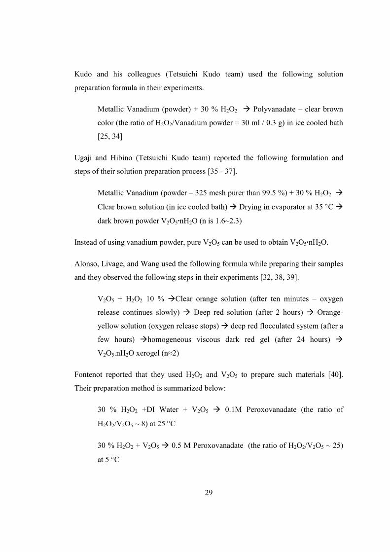
The first step of preparation of coating solution is to obtain a solid material. The
preparation of solid material was started by dissolving metallic vanadium powder
(powder, 325 Mesh purer than 99.5 %) in an iced cooled 30 % H2O2. After the
process, bright reddish solution is obtained. The ratio of vanadium powder to
hydrogen peroxide is 1 g : 100 ml. Figure 2.1 shows the flow diagram of this step.
Vanadium powder + H2O2 (1 g : 100 ml) Bright reddish color solution
31
0.25 g of Vanadium Powder 25 ml Hydrogen Peroxide
Ice cooled bath 2°°°°C for 4-6 h
and continuous stirring at 200 rpm
Figure 2.1 – The flow diagram of first step of the solution preparation. Appropriate amount
of vanadium powder and hydrogen peroxide were mixed in ice cooled bath for 4-6 hours.
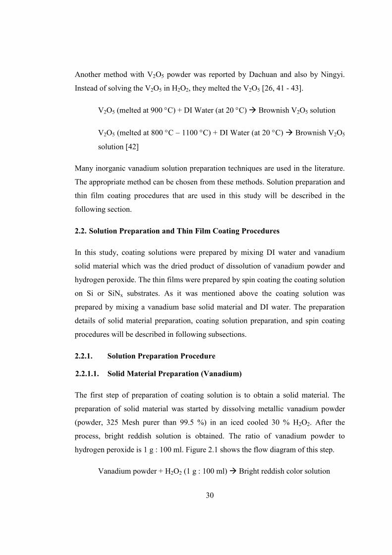
In ambient, an exothermic and violent reaction occurs, when the vanadium powder is
added to hydrogen peroxide. To prevent this violent reaction dissolving process is
done in an ice cooled bath. The solution is kept in iced cooled bath and stirred with
magnetic stirrer (150-200 rpm) until all the vanadium powder dissolved in hydrogen
peroxide. Ice cooled bath provides controllable reaction. However, when an ice
cooled bath is used, the experiment duration becomes very long compare to the
experiment which is done in ambient conditions. Dissolving duration varies between
4 hours to 6 hours when the dissolution done in iced cooled bath. As shown in the
Figure 2.2, the color of the solution changes by the time and it becomes bright
reddish at the end of the process. The color change of the solution is indicating that
the vanadium powder is solved in hydrogen peroxide.
32
(a) (b)
Figure 2.2 – (a) Vanadium - hydrogen peroxide mixture in iced cooled bath (2 ºC)in the
beginning of the dissolution process. (b) light red color mixture after a couple hours (4 hours
– 6 hours).
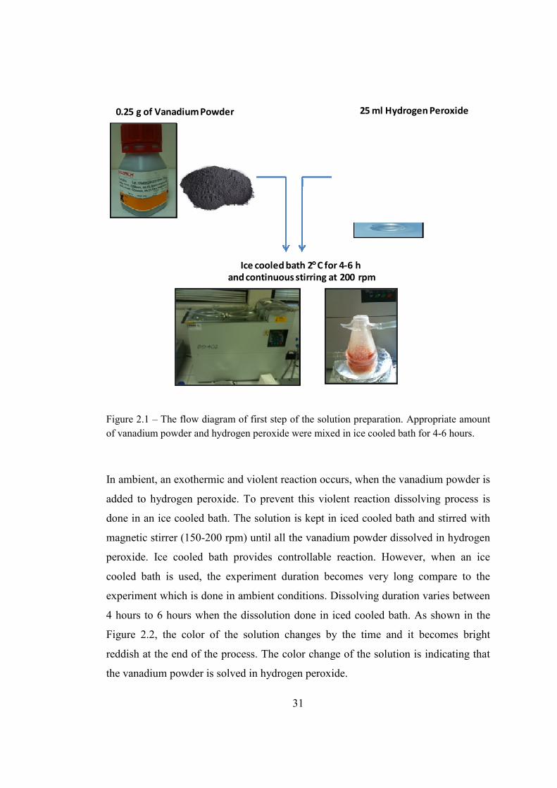
The solution is removed from iced cooled bath after assuring that all the vanadium
powder is dissolved. It can be kept at room temperature or in a hot (50 °C) water
bath. The reaction time decreases when the solution was put in to a hot water bath.
An oxygen release reaction is occurred at the end of the process. Highly exothermic
decomposition of hydrogen peroxide reaction is occurred. Figure 2.3 shows the
moments of this exothermic decomposition.
Violent bubbling of oxygen occurs during the reaction. Oxygen release rate gets
higher by the time, after the sol is taken to the rest. The amount of oxygen release is
increase with time till the higher rate of oxygen release (violent bubbling) occurs.
The bubbling occurs in 30 minutes to 60 minutes in ambient or in 2 minutes in hot
water bath and then oxygen release suddenly stops. The temperature of the solution
is higher than room temperature when the reaction is stopped.
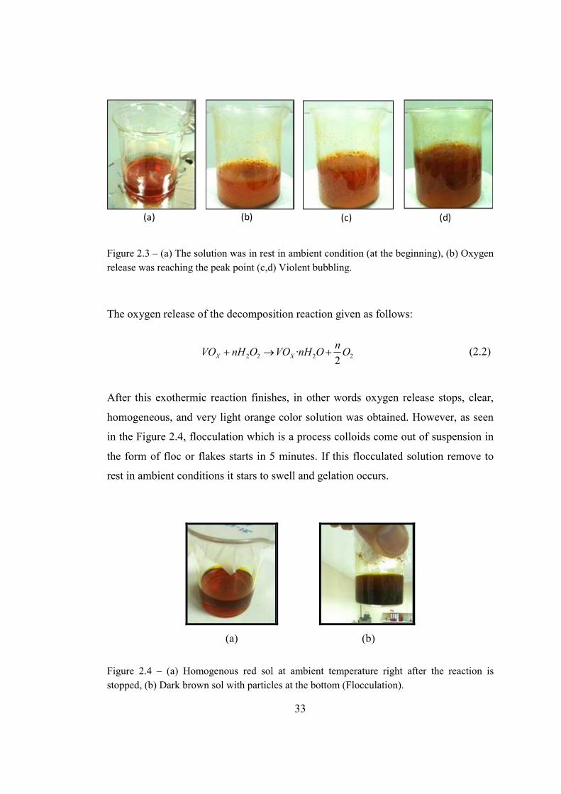
33
(a) (b) (c) (d)
Figure 2.3 – (a) The solution was in rest in ambient condition (at the beginning), (b) Oxygen
release was reaching the peak point (c,d) Violent bubbling.
The oxygen release of the decomposition reaction given as follows:
22222
· On
OnHVOOnHVO XX +→+ (2.2)
After this exothermic reaction finishes, in other words oxygen release stops, clear,
homogeneous, and very light orange color solution was obtained. However, as seen
in the Figure 2.4, flocculation which is a process colloids come out of suspension in
the form of floc or flakes starts in 5 minutes. If this flocculated solution remove to
rest in ambient conditions it stars to swell and gelation occurs.
(a) (b)
Figure 2.4 – (a) Homogenous red sol at ambient temperature right after the reaction is
stopped, (b) Dark brown sol with particles at the bottom (Flocculation).
34
However, decomposition reaction of hydrogen peroxide is not controllable, so the
features of the final product of such gel like solution differ for every trial. To control
the homogeneity, viscosity, and the amount of the solution, the flocculated solution
is put into oven at 80 °C for 24 hours to achieve a solid material. Figure 2.5 shows
the moments of the drying process of the sol. Figure 2.6 shows final product of this
drying process.
(a) (b)
Figure 2.5 – Top view from the drying cup (a) after 12 hours the material does not dry, it is
not liquid also (b) after 24 hours it becomes solid.
Figure 2.6 – The solid material obtained after 24 hours drying process.
To understand the features of the solid material, it is characterized by XRD and
TGA. As shown in Figure 2.7, the solid material is powdered by pounding in a
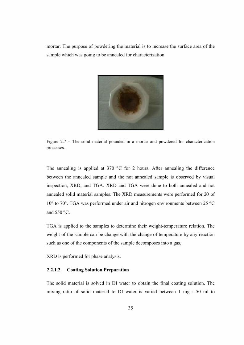
35
mortar. The purpose of powdering the material is to increase the surface area of the
sample which was going to be annealed for characterization.
Figure 2.7 – The solid material pounded in a mortar and powdered for characterization
processes.
The annealing is applied at 370 °C for 2 hours. After annealing the difference
between the annealed sample and the not annealed sample is observed by visual
inspection, XRD, and TGA. XRD and TGA were done to both annealed and not
annealed solid material samples. The XRD measurements were performed for 2θ of
10° to 70°. TGA was performed under air and nitrogen environments between 25 °C
and 550 °C.
TGA is applied to the samples to determine their weight-temperature relation. The
weight of the sample can be change with the change of temperature by any reaction
such as one of the components of the sample decomposes into a gas.
XRD is performed for phase analysis.
2.2.1.2. Coating Solution Preparation
The solid material is solved in DI water to obtain the final coating solution. The
mixing ratio of solid material to DI water is varied between 1 mg : 50 ml to
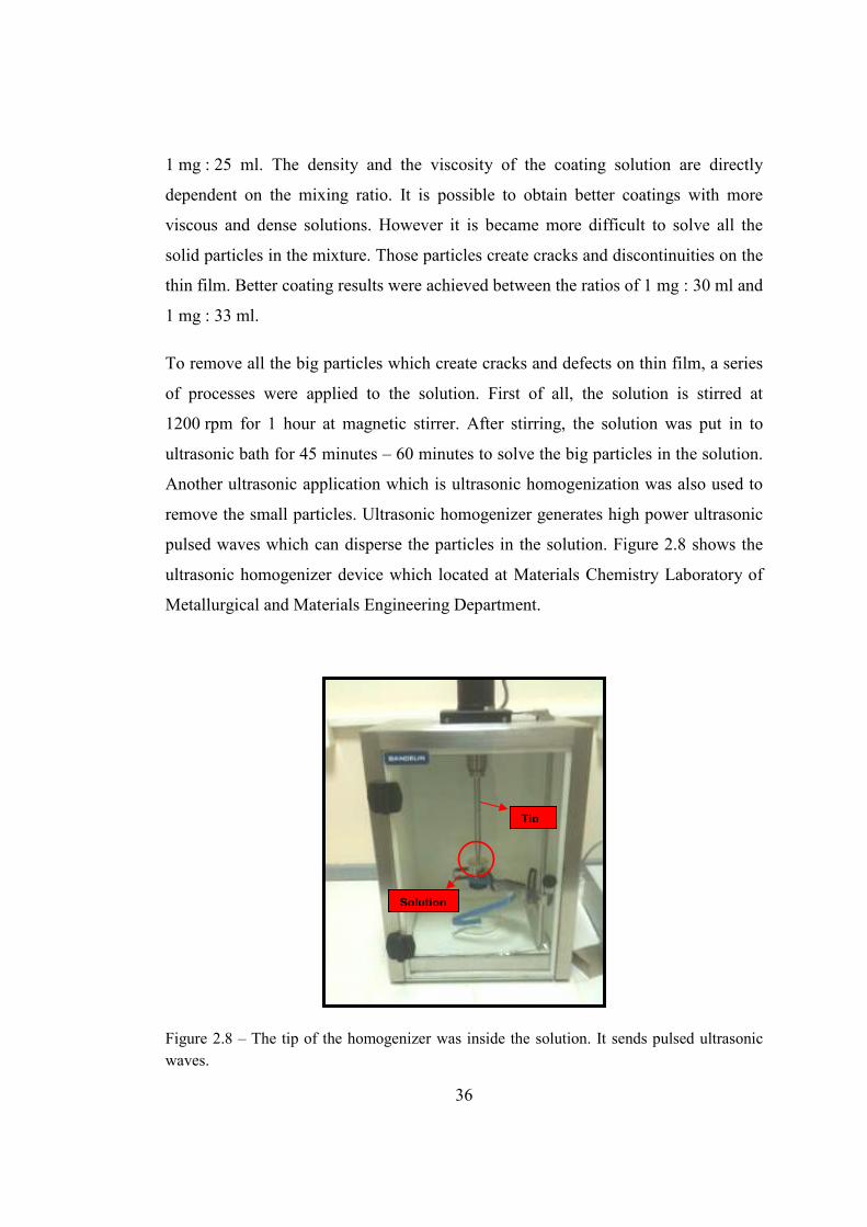
36
1 mg : 25 ml. The density and the viscosity of the coating solution are directly
dependent on the mixing ratio. It is possible to obtain better coatings with more
viscous and dense solutions. However it is became more difficult to solve all the
solid particles in the mixture. Those particles create cracks and discontinuities on the
thin film. Better coating results were achieved between the ratios of 1 mg : 30 ml and
1 mg : 33 ml.
To remove all the big particles which create cracks and defects on thin film, a series
of processes were applied to the solution. First of all, the solution is stirred at
1200 rpm for 1 hour at magnetic stirrer. After stirring, the solution was put in to
ultrasonic bath for 45 minutes – 60 minutes to solve the big particles in the solution.
Another ultrasonic application which is ultrasonic homogenization was also used to
remove the small particles. Ultrasonic homogenizer generates high power ultrasonic
pulsed waves which can disperse the particles in the solution. Figure 2.8 shows the
ultrasonic homogenizer device which located at Materials Chemistry Laboratory of
Metallurgical and Materials Engineering Department.
Figure 2.8 – The tip of the homogenizer was inside the solution. It sends pulsed ultrasonic
waves.
Solution
Tip
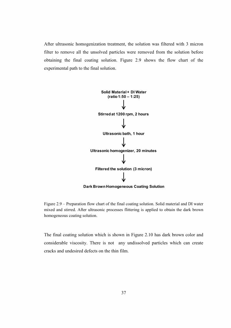
37
After ultrasonic homogenization treatment, the solution was filtered with 3 micron
filter to remove all the unsolved particles were removed from the solution before
obtaining the final coating solution. Figure 2.9 shows the flow chart of the
experimental path to the final solution.
Ultrasonic homogenizer, 20 minutes
Stirred at 1200 rpm, 2 hours
Ultrasonic bath, 1 hour
Filtered the solution (3 micron)
Dark Brown Homogeneous Coating Solution
Solid Material + DI Water(ratio 1:50 – 1:25)
Figure 2.9 – Preparation flow chart of the final coating solution. Solid material and DI water
mixed and stirred. After ultrasonic processes flittering is applied to obtain the dark brown
homogeneous coating solution.
The final coating solution which is shown in Figure 2.10 has dark brown color and
considerable viscosity. There is not any undissolved particles which can create
cracks and undesired defects on the thin film.
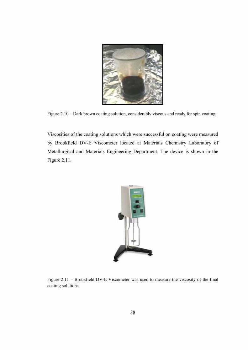
38
Figure 2.10 – Dark brown coating solution, considerably viscous and ready for spin coating.
Viscosities of the coating solutions which were successful on coating were measured
by Brookfield DV-E Viscometer located at Materials Chemistry Laboratory of
Metallurgical and Materials Engineering Department. The device is shown in the
Figure 2.11.
Figure 2.11 – Brookfield DV-E Viscometer was used to measure the viscosity of the final
coating solutions.
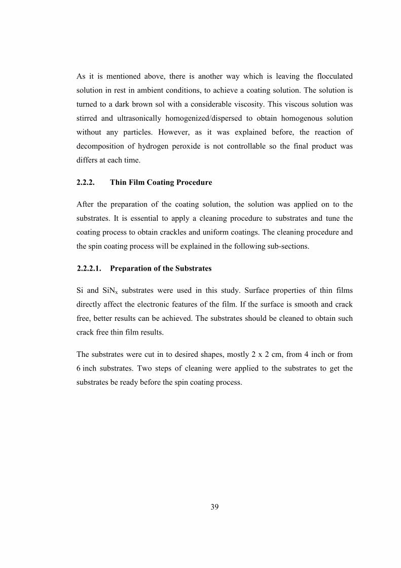
39
As it is mentioned above, there is another way which is leaving the flocculated
solution in rest in ambient conditions, to achieve a coating solution. The solution is
turned to a dark brown sol with a considerable viscosity. This viscous solution was
stirred and ultrasonically homogenized/dispersed to obtain homogenous solution
without any particles. However, as it was explained before, the reaction of
decomposition of hydrogen peroxide is not controllable so the final product was
differs at each time.
2.2.2. Thin Film Coating Procedure
After the preparation of the coating solution, the solution was applied on to the
substrates. It is essential to apply a cleaning procedure to substrates and tune the
coating process to obtain crackles and uniform coatings. The cleaning procedure and
the spin coating process will be explained in the following sub-sections.
2.2.2.1. Preparation of the Substrates
Si and SiNx substrates were used in this study. Surface properties of thin films
directly affect the electronic features of the film. If the surface is smooth and crack
free, better results can be achieved. The substrates should be cleaned to obtain such
crack free thin film results.
The substrates were cut in to desired shapes, mostly 2 x 2 cm, from 4 inch or from
6 inch substrates. Two steps of cleaning were applied to the substrates to get the
substrates be ready before the spin coating process.
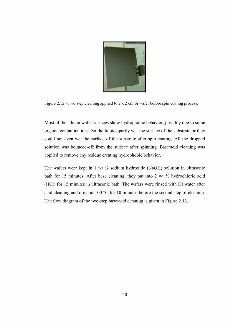
40
Figure 2.12 –Two step cleaning applied to 2 x 2 cm Si wafer before spin coating process.
Most of the silicon wafer surfaces show hydrophobic behavior, possibly due to some
organic contaminations. So the liquids partly wet the surface of the substrate or they
could not even wet the surface of the substrate after spin coating. All the dropped
solution was bounced-off from the surface after spinning. Base/acid cleaning was
applied to remove any residue creating hydrophobic behavior.
The wafers were kept in 1 wt % sodium hydroxide (NaOH) solution in ultrasonic
bath for 15 minutes. After base cleaning, they put into 2 wt % hydrochloric acid
(HCl) for 15 minutes in ultrasonic bath. The wafers were rinsed with DI water after
acid cleaning and dried at 100 °C for 10 minutes before the second step of cleaning.
The flow diagram of the two-step base/acid cleaning is given in Figure 2.13.
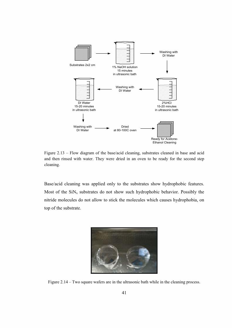
41
Substrates 2x2 cm1% NaOH solution
15 minutes
in ultrasonic bath
Washing with
DI Water
2%HCl
15-20 minutes
in ultrasonic bath
Washing with
DI Water
DI Water
15-20 minutes
in ultrasonic bath
Washing with
DI Water
Dried
at 80-100C oven
Ready for Acetone-
Ethanol Cleaning
Figure 2.13 – Flow diagram of the base/acid cleaning, substrates cleaned in base and acid
and then rinsed with water. They were dried in an oven to be ready for the second step
cleaning.
Base/acid cleaning was applied only to the substrates show hydrophobic features.
Most of the SiNx substrates do not show such hydrophobic behavior. Possibly the
nitride molecules do not allow to stick the molecules which causes hydrophobia, on
top of the substrate.
Figure 2.14 – Two square wafers are in the ultrasonic bath while in the cleaning process.
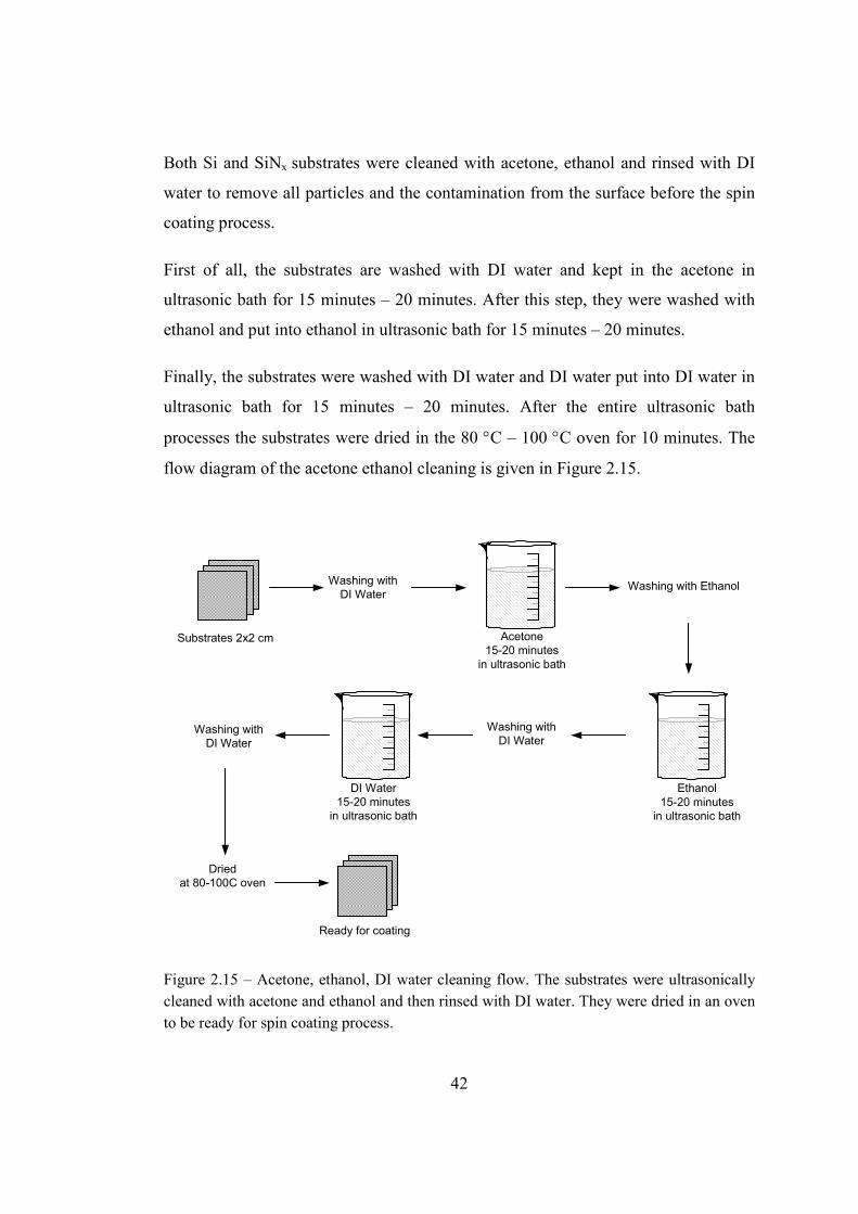
42
Both Si and SiNx substrates were cleaned with acetone, ethanol and rinsed with DI
water to remove all particles and the contamination from the surface before the spin
coating process.
First of all, the substrates are washed with DI water and kept in the acetone in
ultrasonic bath for 15 minutes – 20 minutes. After this step, they were washed with
ethanol and put into ethanol in ultrasonic bath for 15 minutes – 20 minutes.
Finally, the substrates were washed with DI water and DI water put into DI water in
ultrasonic bath for 15 minutes – 20 minutes. After the entire ultrasonic bath
processes the substrates were dried in the 80 °C – 100 °C oven for 10 minutes. The
flow diagram of the acetone ethanol cleaning is given in Figure 2.15.
Substrates 2x2 cm Acetone
15-20 minutes
in ultrasonic bath
Washing with Ethanol
Ready for coating
Dried
at 80-100C oven
Washing with
DI Water
Washing with
DI Water
Ethanol
15-20 minutes
in ultrasonic bath
DI Water
15-20 minutes
in ultrasonic bath
Washing with
DI Water
Figure 2.15 – Acetone, ethanol, DI water cleaning flow. The substrates were ultrasonically
cleaned with acetone and ethanol and then rinsed with DI water. They were dried in an oven
to be ready for spin coating process.
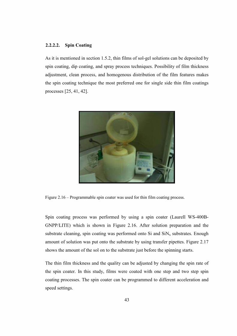
43
2.2.2.2. Spin Coating
As it is mentioned in section 1.5.2, thin films of sol-gel solutions can be deposited by
spin coating, dip coating, and spray process techniques. Possibility of film thickness
adjustment, clean process, and homogenous distribution of the film features makes
the spin coating technique the most preferred one for single side thin film coatings
processes [25, 41, 42].
Figure 2.16 – Programmable spin coater was used for thin film coating process.
Spin coating process was performed by using a spin coater (Laurell WS-400B-
GNPP/LITE) which is shown in Figure 2.16. After solution preparation and the
substrate cleaning, spin coating was performed onto Si and SiNx substrates. Enough
amount of solution was put onto the substrate by using transfer pipettes. Figure 2.17
shows the amount of the sol on to the substrate just before the spinning starts.
The thin film thickness and the quality can be adjusted by changing the spin rate of
the spin coater. In this study, films were coated with one step and two step spin
coating processes. The spin coater can be programmed to different acceleration and
speed settings.
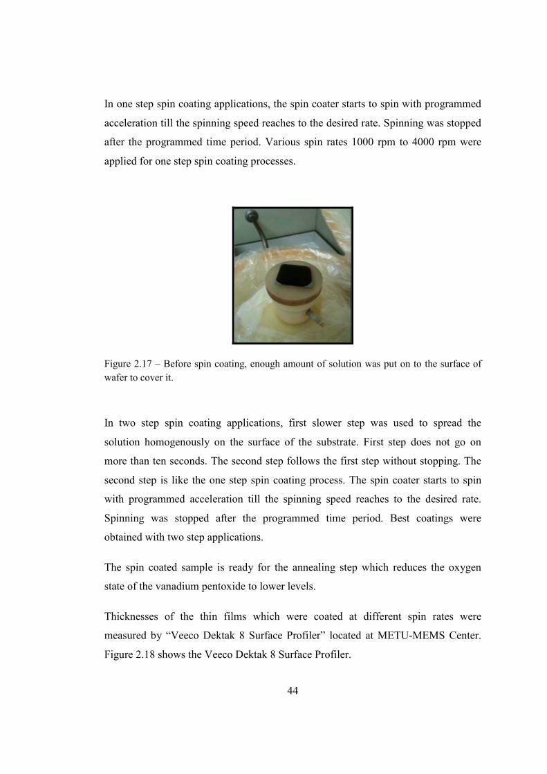
44
In one step spin coating applications, the spin coater starts to spin with programmed
acceleration till the spinning speed reaches to the desired rate. Spinning was stopped
after the programmed time period. Various spin rates 1000 rpm to 4000 rpm were
applied for one step spin coating processes.
Figure 2.17 – Before spin coating, enough amount of solution was put on to the surface of
wafer to cover it.
In two step spin coating applications, first slower step was used to spread the
solution homogenously on the surface of the substrate. First step does not go on
more than ten seconds. The second step follows the first step without stopping. The
second step is like the one step spin coating process. The spin coater starts to spin
with programmed acceleration till the spinning speed reaches to the desired rate.
Spinning was stopped after the programmed time period. Best coatings were
obtained with two step applications.
The spin coated sample is ready for the annealing step which reduces the oxygen
state of the vanadium pentoxide to lower levels.
Thicknesses of the thin films which were coated at different spin rates were
measured by “Veeco Dektak 8 Surface Profiler” located at METU-MEMS Center.
Figure 2.18 shows the Veeco Dektak 8 Surface Profiler.
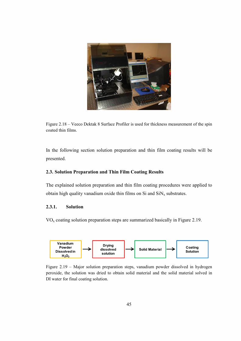
45
Figure 2.18 – Veeco Dektak 8 Surface Profiler is used for thickness measurement of the spin
coated thin films.
In the following section solution preparation and thin film coating results will be
presented.
2.3. Solution Preparation and Thin Film Coating Results
The explained solution preparation and thin film coating procedures were applied to
obtain high quality vanadium oxide thin films on Si and SiNx substrates.
2.3.1. Solution
VOx coating solution preparation steps are summarized basically in Figure 2.19.
VanadiumPowder
Dissolved in
H2O2
Solid MaterialCoating
Solution
Dryingdissolved
solution
Figure 2.19 – Major solution preparation steps, vanadium powder dissolved in hydrogen
peroxide, the solution was dried to obtain solid material and the solid material solved in
DI water for final coating solution.
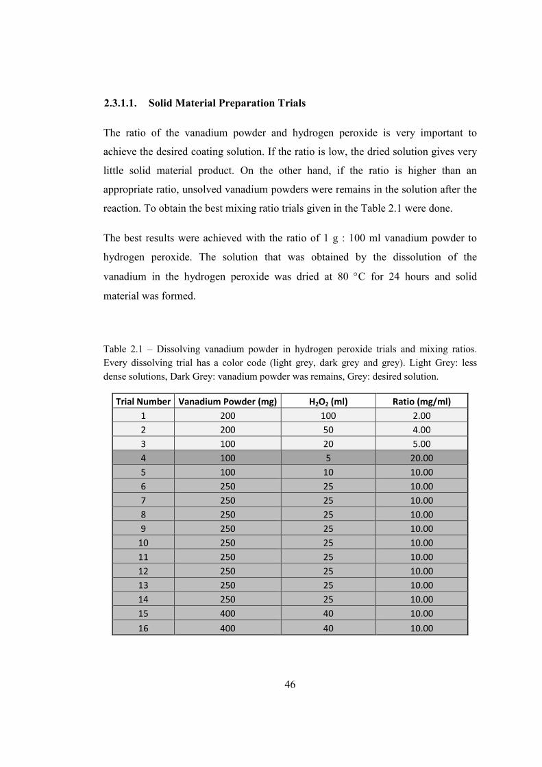
46
2.3.1.1. Solid Material Preparation Trials
The ratio of the vanadium powder and hydrogen peroxide is very important to
achieve the desired coating solution. If the ratio is low, the dried solution gives very
little solid material product. On the other hand, if the ratio is higher than an
appropriate ratio, unsolved vanadium powders were remains in the solution after the
reaction. To obtain the best mixing ratio trials given in the Table 2.1 were done.
The best results were achieved with the ratio of 1 g : 100 ml vanadium powder to
hydrogen peroxide. The solution that was obtained by the dissolution of the
vanadium in the hydrogen peroxide was dried at 80 °C for 24 hours and solid
material was formed.
Table 2.1 – Dissolving vanadium powder in hydrogen peroxide trials and mixing ratios.
Every dissolving trial has a color code (light grey, dark grey and grey). Light Grey: less
dense solutions, Dark Grey: vanadium powder was remains, Grey: desired solution.
Trial Number Vanadium Powder (mg) H2O2 (ml) Ratio (mg/ml)
1 200 100 2.00
2 200 50 4.00
3 100 20 5.00
4 100 5 20.00
5 100 10 10.00
6 250 25 10.00
7 250 25 10.00
8 250 25 10.00
9 250 25 10.00
10 250 25 10.00
11 250 25 10.00
12 250 25 10.00
13 250 25 10.00
14 250 25 10.00
15 400 40 10.00
16 400 40 10.00
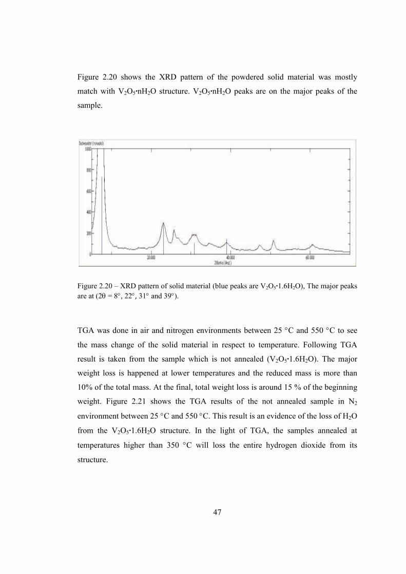
47
Figure 2.20 shows the XRD pattern of the powdered solid material was mostly
match with V2O5·nH2O structure. V2O5·nH2O peaks are on the major peaks of the
sample.
Figure 2.20 – XRD pattern of solid material (blue peaks are V2O5·1.6H2O), The major peaks
are at (2θ = 8°, 22°, 31° and 39°).
TGA was done in air and nitrogen environments between 25 °C and 550 °C to see
the mass change of the solid material in respect to temperature. Following TGA
result is taken from the sample which is not annealed (V2O5·1.6H2O). The major
weight loss is happened at lower temperatures and the reduced mass is more than
10% of the total mass. At the final, total weight loss is around 15 % of the beginning
weight. Figure 2.21 shows the TGA results of the not annealed sample in N2
environment between 25 °C and 550 °C. This result is an evidence of the loss of H2O
from the V2O5·1.6H2O structure. In the light of TGA, the samples annealed at
temperatures higher than 350 °C will loss the entire hydrogen dioxide from its
structure.
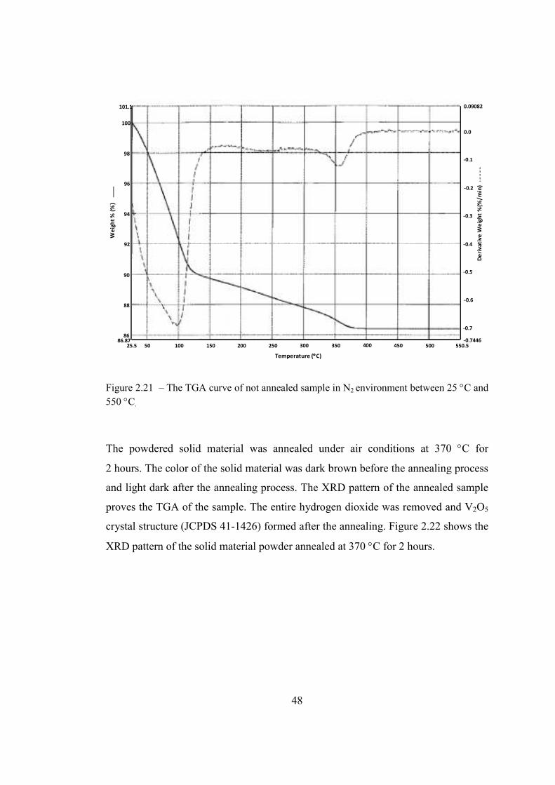
48
101.1
100
98
96
94
92
90
88
8686.87
25.5 50 100 150 200 250 300 350 400 450 500 550.5-0.7446
-0.7
-0.6
-0.5
-0.4
-0.3
-0.2
-0.1
0.0
0.09082W
eig
ht
% (
%)
Temperature (°°°°C)
De
riv
ati
ve
We
igh
t %
(%/
min
)
Figure 2.21 – The TGA curve of not annealed sample in N2 environment between 25 °C and 550 °C.
The powdered solid material was annealed under air conditions at 370 °C for
2 hours. The color of the solid material was dark brown before the annealing process
and light dark after the annealing process. The XRD pattern of the annealed sample
proves the TGA of the sample. The entire hydrogen dioxide was removed and V2O5
crystal structure (JCPDS 41-1426) formed after the annealing. Figure 2.22 shows the
XRD pattern of the solid material powder annealed at 370 °C for 2 hours.
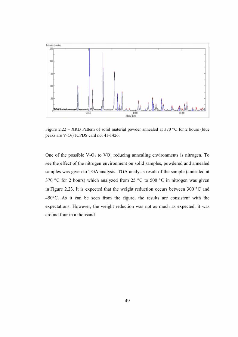
49
Figure 2.22 – XRD Pattern of solid material powder annealed at 370 °C for 2 hours (blue peaks are V2O5) JCPDS card no: 41-1426.
One of the possible V2O5 to VOx reducing annealing environments is nitrogen. To
see the effect of the nitrogen environment on solid samples, powdered and annealed
samples was given to TGA analysis. TGA analysis result of the sample (annealed at
370 °C for 2 hours) which analyzed from 25 °C to 500 °C in nitrogen was given
in Figure 2.23. It is expected that the weight reduction occurs between 300 °C and
450°C. As it can be seen from the figure, the results are consistent with the
expectations. However, the weight reduction was not as much as expected, it was
around four in a thousand.
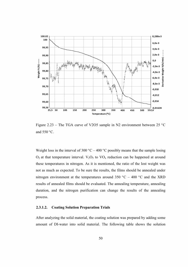
50
-2,0e-3
100
100.02
99,95
99,90
99,85
99,80
99,75
99,70
99,56
We
igh
t %
(%
)
25,5 50 100 150 200 250 300 350 400 450 500 552,6
Temperature (°°°°C)
0,0
8,288e-3
2,0e-3
-4,0e-3
-6,0e-3
-8,0e-3
-0,010
-0,012
-0,014
-0,01628
De
riv
ati
ve
We
igh
t %
(%/
min
)
99,65
99,60
4,0e-3
6,0e-3
Figure 2.23 – The TGA curve of V2O5 sample in N2 environment between 25 °C
and 550 °C.
Weight loss in the interval of 300 °C – 400 °C possibly means that the sample losing
O2 at that temperature interval. V2O5 to VOx reduction can be happened at around
these temperatures in nitrogen. As it is mentioned, the ratio of the lost weight was
not as much as expected. To be sure the results, the films should be annealed under
nitrogen environment at the temperatures around 350 °C – 400 °C and the XRD
results of annealed films should be evaluated. The annealing temperature, annealing
duration, and the nitrogen purification can change the results of the annealing
process.
2.3.1.2. Coating Solution Preparation Trials
After analyzing the solid material, the coating solution was prepared by adding some
amount of DI-water into solid material. The following table shows the solution
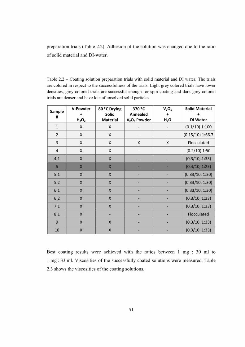
51
preparation trials (Table 2.2). Adhesion of the solution was changed due to the ratio
of solid material and DI-water.
Table 2.2 – Coating solution preparation trials with solid material and DI water. The trials
are colored in respect to the successfulness of the trials. Light grey colored trials have lower
densities, grey colored trials are successful enough for spin coating and dark grey colored
trials are denser and have lots of unsolved solid particles.
Sample
#
V-Powder
+
H2O2
80 °°°°C Drying
Solid
Material
370 °°°°C
Annealed
V2O5 Powder
V2O5
+
H2O
Solid Material
+
DI Water
1 X X - - (0.1/10) 1:100
2 X X - - (0.15/10) 1:66.7
3 X X X X Flocculated
4 X X - - (0.2/10) 1:50
4.1 X X - - (0.3/10, 1:33)
5 X X - - (0.4/10, 1:25)
5.1 X X - - (0.33/10, 1:30)
5.2 X X - - (0.33/10, 1:30)
6.1 X X - - (0.33/10, 1:30)
6.2 X X - - (0.3/10, 1:33)
7.1 X X - - (0.3/10, 1:33)
8.1 X - - - Flocculated
9 X X - - (0.3/10, 1:33)
10 X X - - (0.3/10, 1:33)
Best coating results were achieved with the ratios between 1 mg : 30 ml to
1 mg : 33 ml. Viscosities of the successfully coated solutions were measured. Table
2.3 shows the viscosities of the coating solutions.
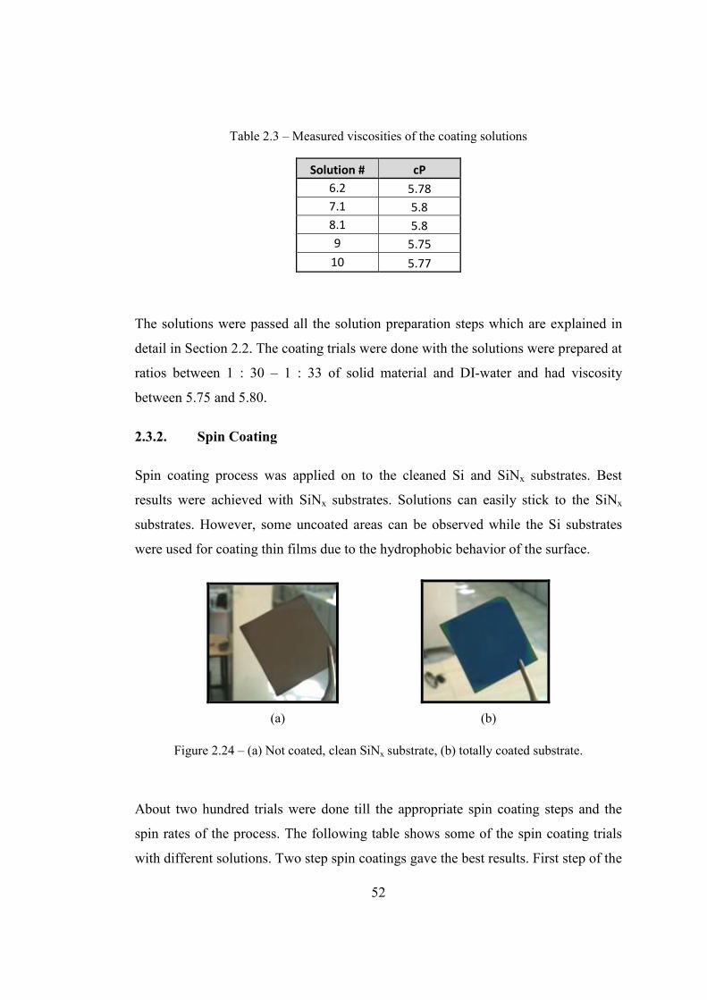
52
Table 2.3 – Measured viscosities of the coating solutions
Solution # cP
6.2 5.78
7.1 5.8
8.1 5.8
9 5.75
10 5.77
The solutions were passed all the solution preparation steps which are explained in
detail in Section 2.2. The coating trials were done with the solutions were prepared at
ratios between 1 : 30 – 1 : 33 of solid material and DI-water and had viscosity
between 5.75 and 5.80.
2.3.2. Spin Coating
Spin coating process was applied on to the cleaned Si and SiNx substrates. Best
results were achieved with SiNx substrates. Solutions can easily stick to the SiNx
substrates. However, some uncoated areas can be observed while the Si substrates
were used for coating thin films due to the hydrophobic behavior of the surface.
(a) (b)
Figure 2.24 – (a) Not coated, clean SiNx substrate, (b) totally coated substrate.
About two hundred trials were done till the appropriate spin coating steps and the
spin rates of the process. The following table shows some of the spin coating trials
with different solutions. Two step spin coatings gave the best results. First step of the
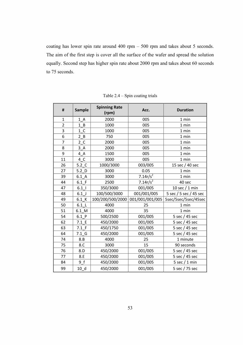
53
coating has lower spin rate around 400 rpm – 500 rpm and takes about 5 seconds.
The aim of the first step is cover all the surface of the wafer and spread the solution
equally. Second step has higher spin rate about 2000 rpm and takes about 60 seconds
to 75 seconds.
Table 2.4 – Spin coating trials
# Sample Spinning Rate
(rpm) Acc. Duration
1 1_A 2000 005 1 min
2 1_B 1000 005 1 min
3 1_C 1000 005 1 min
6 2_B 750 005 1 min
7 2_C 2000 005 1 min
8 3_A 2000 005 1 min
9 4_A 1500 005 1 min
11 4_C 3000 005 1 min
26 5.2_C 1000/3000 003/005 15 sec / 40 sec
27 5.2_D 3000 0.05 1 min
39 6.1_A 3000 7.14r/s2 1 min
44 6.1_F 2500 7.14r/s2 40 sec
47 6.1_I 350/3000 001/005 10 sec / 1 min
48 6.1_J 100/500/3000 001/001/005 5 sec / 5 sec / 45 sec
49 6.1_K 100/200/500/2000 001/001/001/005 5sec/5sec/5sec/45sec
50 6.1_L 4000 25 1 min
51 6.1_M 4000 35 1 min
54 6.1_P 500/2500 001/005 5 sec / 45 sec
62 7.1_E 450/2000 001/005 5 sec / 45 sec
63 7.1_F 450/1750 001/005 5 sec / 45 sec
64 7.1_G 450/2000 001/005 5 sec / 45 sec
74 8.B 4000 25 1 minute
75 8.C 3000 15 90 seconds
76 8.D 450/2000 001/005 5 sec / 45 sec
77 8.E 450/2000 001/005 5 sec / 45 sec
84 9_f 450/2000 001/005 5 sec / 1 min
99 10_d 450/2000 001/005 5 sec / 75 sec
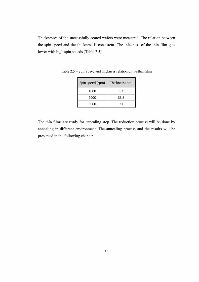
54
Thicknesses of the successfully coated wafers were measured. The relation between
the spin speed and the thickness is consistent. The thickness of the thin film gets
lower with high spin speeds (Table 2.5).
Table 2.5 – Spin speed and thickness relation of the thin films
Spin speed (rpm) Thickness (nm)
1000 57
2000 33.5
3000 21
The thin films are ready for annealing step. The reduction process will be done by
annealing in different environment. The annealing process and the results will be
presented in the following chapter.
55
CHAPTER 3
ANNEALING OF VOx THIN FILMS
Annealing is used to create crystal structures or increase/decrease the oxygen states
of the metal oxide thin films. Different annealing environments such as air, vacuum,
nitrogen, hydrogen, CO, CO2, and some other gas mixtures used as reducing
annealing atmospheres. [25, 28, 31, 32, 41, 44]. Annealing atmosphere, temperature
and duration are the critical parameters for annealing process. It is possible to change
the result of the process by changing these critical parameters.
This chapter presents the annealing procedure and the characterization of the VOx
thin films. Section 3.1 gives information about the annealing trials of vanadium
oxide thin films in the literature. Section 3.2 describes the annealing procedures to
reduce the oxygen state of the VOx and Section 3.3 summarizes the results of the
annealing process.
3.1. Annealing Trials of VOx Films in the Literature
It is possible to reduce the oxygen state of VOx with annealing atmospheres such as
air, vacuum, nitrogen, hydrogen, CO, CO2, and some other gas mixtures; however,
as it was mentioned annealing temperature and the duration of the annealing are the
other critical parameters for reduction process. There are many possible
stochiometries and structures of vanadium oxide such as VO, V2O3, VO2, V3O7,
V4O9, V6O13, V2O5 [31, 45, 46].
The following table shows the results of VOx annealing under different
environments, durations, and pressures (Table 3.1). When the literature was surveyed
many teams used various annealing processes to reduce the oxygen state of the VOx.
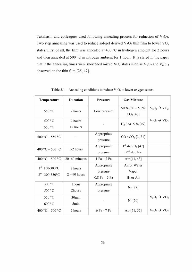
56
Takahashi and colleagues used following annealing process for reduction of V2O5.
Two step annealing was used to reduce sol-gel derived V2O5 thin film to lower VOx
states. First of all, the film was annealed at 400 °C in hydrogen ambient for 2 hours
and then annealed at 500 °C in nitrogen ambient for 1 hour. It is stated in the paper
that if the annealing times were shortened mixed VOx states such as V3O7 and V6O13
observed on the thin film [25, 47].
Table 3.1 – Annealing conditions to reduce V2O5 to lower oxygen states.
Temperature Duration Pressure Gas Mixture
550 °C 2 hours Low pressure 50 % CO – 50 %
CO2 [48]
V2O5 VO2
500 °C
550 °C
2 hours
12 hours - H2 / Ar 5 % [49]
V2O5 VO2
500 °C – 550 °C - Appropriate
pressure CO / CO2 [3, 31]
400 °C – 500 °C 1-2 hours Appropriate
pressure
1st step H2 [47]
2nd step N2
400 °C – 500 °C 20 -60 minutes 1 Pa – 2 Pa Air [41, 43]
1st 150-300°C
2nd 300-550°C
2 hours
2 – 90 hours
Appropriate
pressure
0.8 Pa – 5 Pa
Air or Water
Vapor
H2 or Air
300 °C
500 °C
1hour
2hours
Appropriate
pressure N2 [27]
550 °C
600 °C
30min
5min - N2 [50]
V2O5 VO2
400 °C – 500 °C 2 hours 6 Pa - 7 Pa Air [51, 52] V2O5 VO2
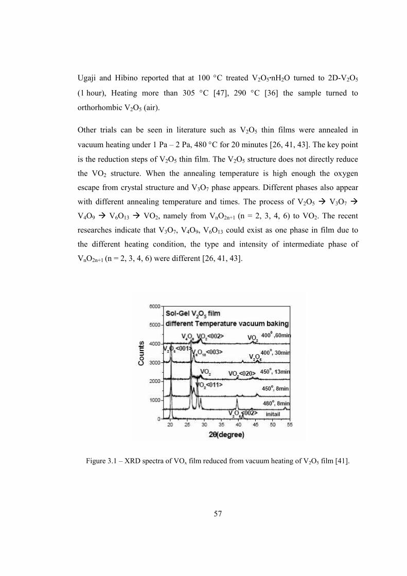
57
Ugaji and Hibino reported that at 100 °C treated V2O5·nH2O turned to 2D-V2O5
(1 hour), Heating more than 305 °C [47], 290 °C [36] the sample turned to
orthorhombic V2O5 (air).
Other trials can be seen in literature such as V2O5 thin films were annealed in
vacuum heating under 1 Pa – 2 Pa, 480 °C for 20 minutes [26, 41, 43]. The key point
is the reduction steps of V2O5 thin film. The V2O5 structure does not directly reduce
the VO2 structure. When the annealing temperature is high enough the oxygen
escape from crystal structure and V3O7 phase appears. Different phases also appear
with different annealing temperature and times. The process of V2O5 V3O7
V4O9 V6O13 VO2, namely from VnO2n+1 (n = 2, 3, 4, 6) to VO2. The recent
researches indicate that V3O7, V4O9, V6O13 could exist as one phase in film due to
the different heating condition, the type and intensity of intermediate phase of
VnO2n+1 (n = 2, 3, 4, 6) were different [26, 41, 43].
Figure 3.1 – XRD spectra of VOx film reduced from vacuum heating of V2O5 film [41].
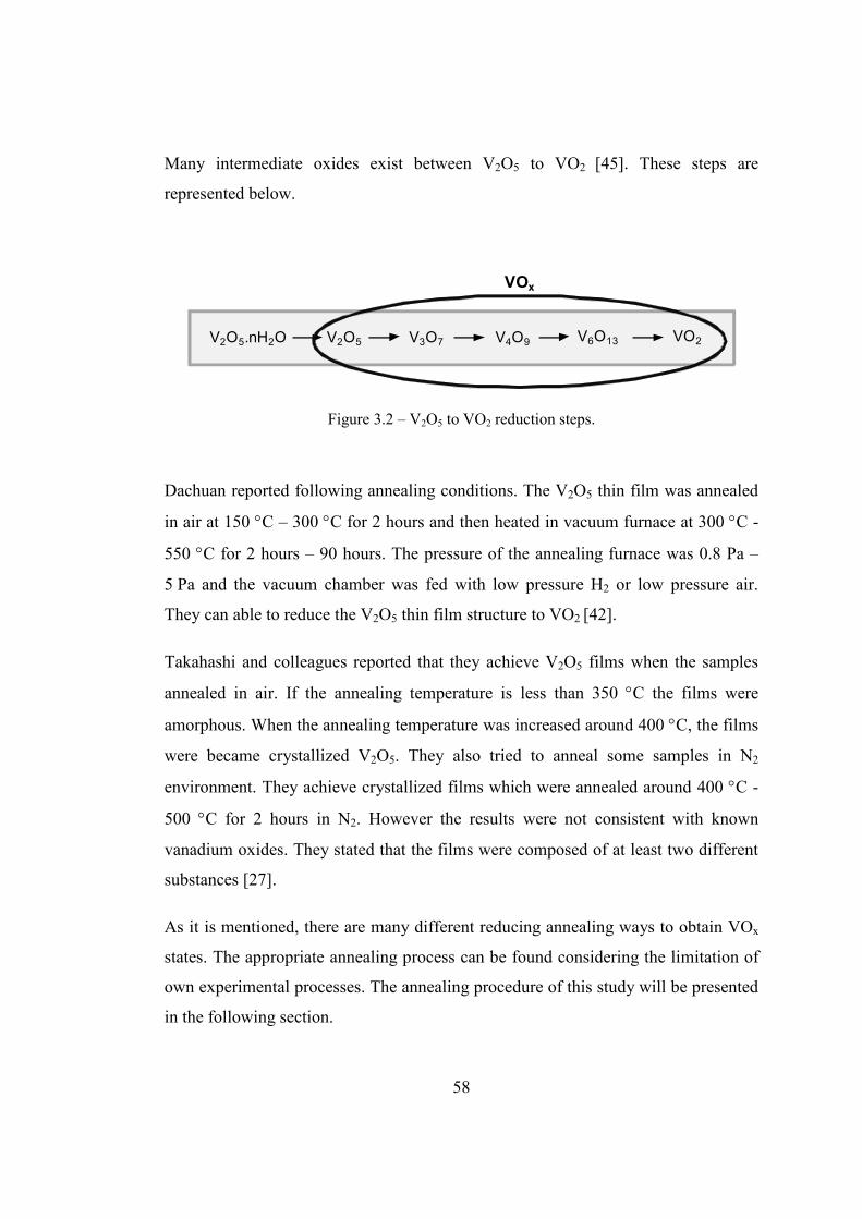
58
Many intermediate oxides exist between V2O5 to VO2 [45]. These steps are
represented below.
V2O5.nH2O V2O5 V3O7 V4O9 V6O13 VO2
VOx
Figure 3.2 – V2O5 to VO2 reduction steps.
Dachuan reported following annealing conditions. The V2O5 thin film was annealed
in air at 150 °C – 300 °C for 2 hours and then heated in vacuum furnace at 300 °C -
550 °C for 2 hours – 90 hours. The pressure of the annealing furnace was 0.8 Pa –
5 Pa and the vacuum chamber was fed with low pressure H2 or low pressure air.
They can able to reduce the V2O5 thin film structure to VO2 [42].
Takahashi and colleagues reported that they achieve V2O5 films when the samples
annealed in air. If the annealing temperature is less than 350 °C the films were
amorphous. When the annealing temperature was increased around 400 °C, the films
were became crystallized V2O5. They also tried to anneal some samples in N2
environment. They achieve crystallized films which were annealed around 400 °C -
500 °C for 2 hours in N2. However the results were not consistent with known
vanadium oxides. They stated that the films were composed of at least two different
substances [27].
As it is mentioned, there are many different reducing annealing ways to obtain VOx
states. The appropriate annealing process can be found considering the limitation of
own experimental processes. The annealing procedure of this study will be presented
in the following section.
59
3.2. Annealing Procedure
In this study, main reason behind the annealing is reducing the V2O5 thin film
structure to the lower oxygen states of VOx. To achieve this objective many
annealing environments, different temperatures and various annealing periods were
applied to the thin films (Table 3.2).
Table 3.2 – Various annealing trials were tried to find the appropriate annealing procedure.
# Drying Air
370 °°°°C
Air
400 °°°°C
N2
200 °°°°C
N2
370 °°°°C
N2
400 °°°°C
Vacuum
(~E-5 Torr)
400 °°°°C
(RTA)
5%
H2/N2
400 °°°°C
(RTA)
5%
H2/N2
420 °°°°C
(RTA)
25%
H2/N2
400 °°°°C
(RTA)
10%
H2/N2
420 °°°°C
(RTA)
10%
H2/N2
410 °°°°C
(RTA)
20%
H2/N2
410 °°°°C
(RTA)
30%
H2/N2
410 °°°°C
(RTA)
40%
H2/N2
410 °°°°C
(RTA)
1 X
2 X 2 h
3 X 2 h 2 h
4 X 2 h 2 h
5 X 2 h
6 X 2 h
7 X 2 h 5 h
8 X 2 h 2 h
9 X 2 h 2 h
10 X 20 min
11 X 30 min
12 X 45 min
13 X 20 min
14 X 30 min
15 X 2 h (2nd) 2 h (1st)
16 X (2nd) (1st)
17 X (2nd) (1st)
18 X (2nd) (1st)
19 X (2nd) (1st)
Heat treatment of thin films begins with the drying step. Drying was done in an oven
at 80 °C for 30 minutes to 1 hour or it was done in ambient conditions.
Dried films should be annealed after drying process to obtain the desirable VOx
structure. Dried film has amorphous structure which contains vanadium, oxygen and
the hydrogen. Hydrogen dioxide molecules can be observed by XRD on the dried
films. Annealing is removed the undesired hydrogen molecules and the change the
structure of the film amorphous to polycrystal.
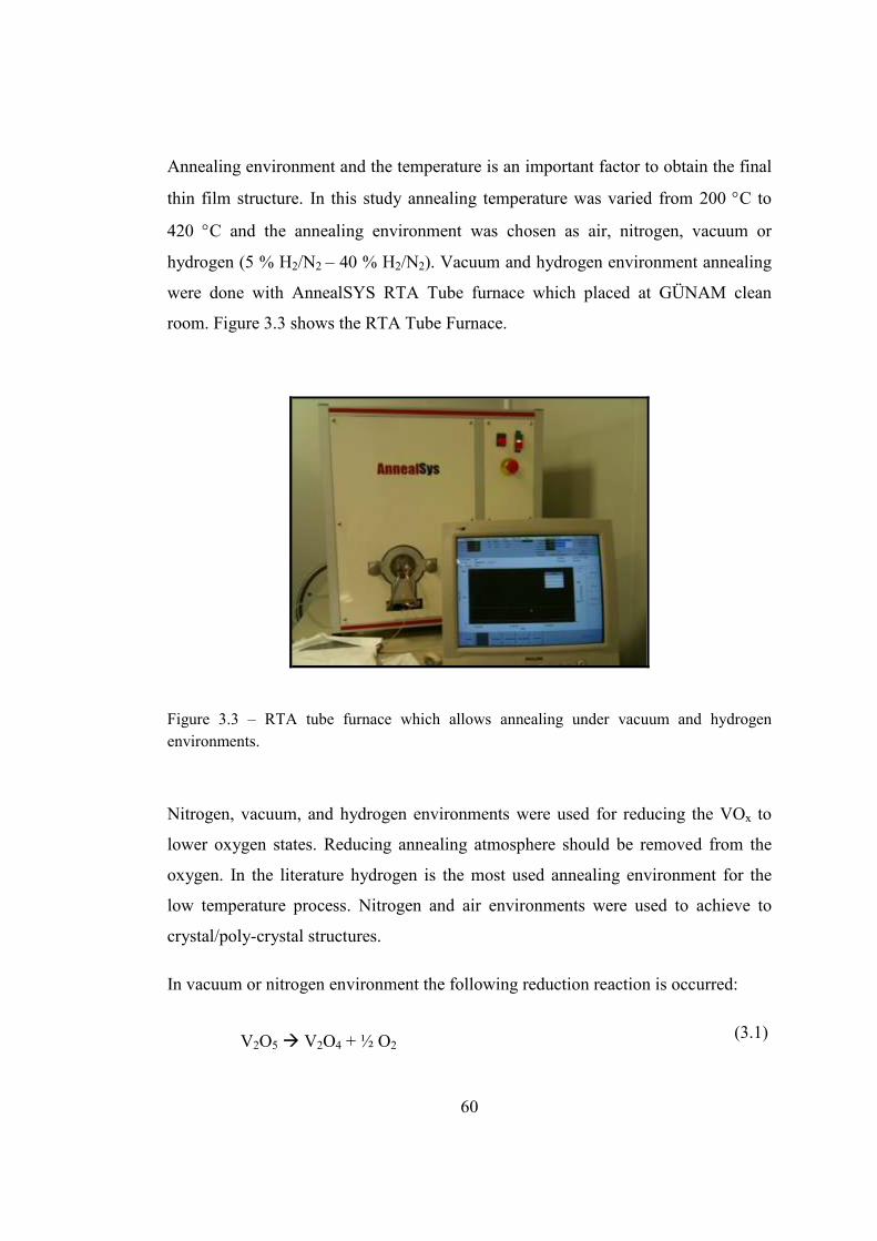
60
Annealing environment and the temperature is an important factor to obtain the final
thin film structure. In this study annealing temperature was varied from 200 °C to
420 °C and the annealing environment was chosen as air, nitrogen, vacuum or
hydrogen (5 % H2/N2 – 40 % H2/N2). Vacuum and hydrogen environment annealing
were done with AnnealSYS RTA Tube furnace which placed at GÜNAM clean
room. Figure 3.3 shows the RTA Tube Furnace.
Figure 3.3 – RTA tube furnace which allows annealing under vacuum and hydrogen
environments.
Nitrogen, vacuum, and hydrogen environments were used for reducing the VOx to
lower oxygen states. Reducing annealing atmosphere should be removed from the
oxygen. In the literature hydrogen is the most used annealing environment for the
low temperature process. Nitrogen and air environments were used to achieve to
crystal/poly-crystal structures.
In vacuum or nitrogen environment the following reduction reaction is occurred:
V2O5 V2O4 + ½ O2 (3.1)
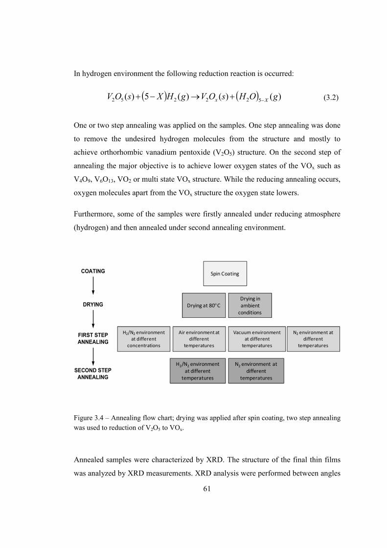
61
In hydrogen environment the following reduction reaction is occurred:
( ) ( ) )()()(5)( 522252 gOHsOVgHXsOVXx −+→−+ (3.2)
One or two step annealing was applied on the samples. One step annealing was done
to remove the undesired hydrogen molecules from the structure and mostly to
achieve orthorhombic vanadium pentoxide (V2O5) structure. On the second step of
annealing the major objective is to achieve lower oxygen states of the VOx such as
V4O9, V6O13, VO2 or multi state VOx structure. While the reducing annealing occurs,
oxygen molecules apart from the VOx structure the oxygen state lowers.
Furthermore, some of the samples were firstly annealed under reducing atmosphere
(hydrogen) and then annealed under second annealing environment.
COATING
DRYING
FIRST STEP
ANNEALING
SECOND STEP
ANNEALING
Spin Coating
Drying at 80°CDrying in
ambient
conditions
H2/N2 environment
at different
concentrations
Air environment at
different
temperatures
Vacuum environment
at different
temperatures
N2 environment at
different
temperatures
H2/N2 environment
at different
temperatures
N2 environment at
different
temperatures
Figure 3.4 – Annealing flow chart; drying was applied after spin coating, two step annealing
was used to reduction of V2O5 to VOx.
Annealed samples were characterized by XRD. The structure of the final thin films
was analyzed by XRD measurements. XRD analysis were performed between angles
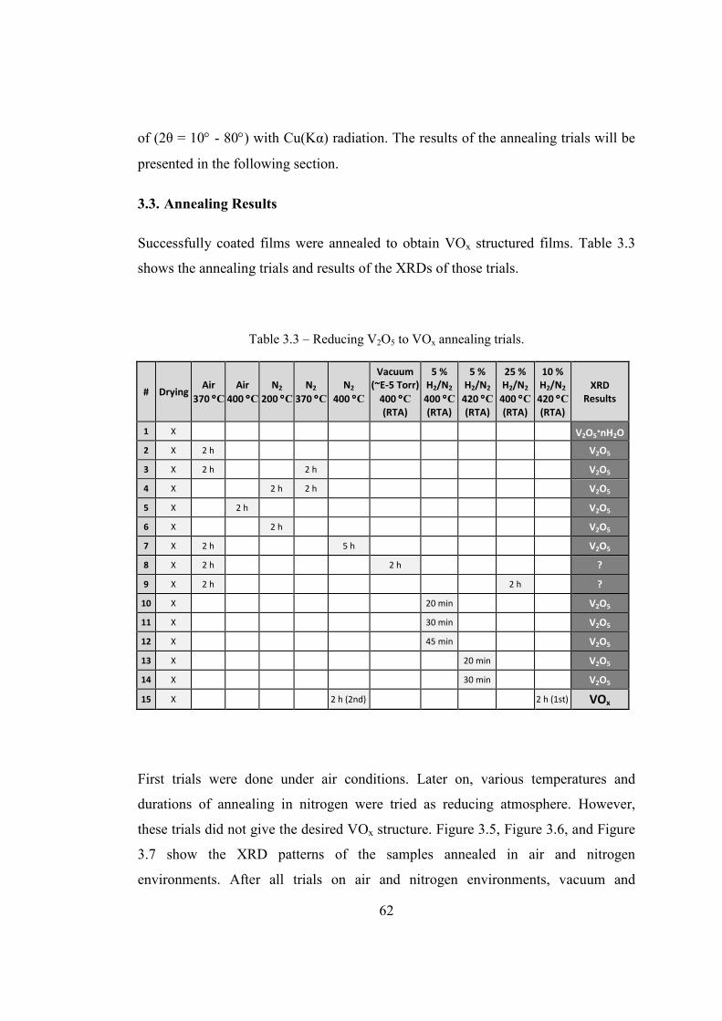
62
of (2θ = 10° - 80°) with Cu(Kα) radiation. The results of the annealing trials will be
presented in the following section.
3.3. Annealing Results
Successfully coated films were annealed to obtain VOx structured films. Table 3.3
shows the annealing trials and results of the XRDs of those trials.
Table 3.3 – Reducing V2O5 to VOx annealing trials.
# Drying Air
370 °°°°C
Air
400 °°°°C
N2
200 °°°°C
N2
370 °°°°C
N2
400 °°°°C
Vacuum
(~E-5 Torr)
400 °°°°C
(RTA)
5 %
H2/N2
400 °°°°C
(RTA)
5 %
H2/N2
420 °°°°C
(RTA)
25 %
H2/N2
400 °°°°C
(RTA)
10 %
H2/N2
420 °°°°C
(RTA)
XRD
Results
1 X V2O5·nH2O
2 X 2 h
V2O5
3 X 2 h
2 h
V2O5
4 X
2 h 2 h
V2O5
5 X
2 h
V2O5
6 X
2 h
V2O5
7 X 2 h
5 h
V2O5
8 X 2 h
2 h
?
9 X 2 h
2 h
?
10 X
20 min
V2O5
11 X
30 min
V2O5
12 X
45 min
V2O5
13 X
20 min
V2O5
14 X
30 min
V2O5
15 X
2 h (2nd)
2 h (1st) VOx
First trials were done under air conditions. Later on, various temperatures and
durations of annealing in nitrogen were tried as reducing atmosphere. However,
these trials did not give the desired VOx structure. Figure 3.5, Figure 3.6, and Figure
3.7 show the XRD patterns of the samples annealed in air and nitrogen
environments. After all trials on air and nitrogen environments, vacuum and
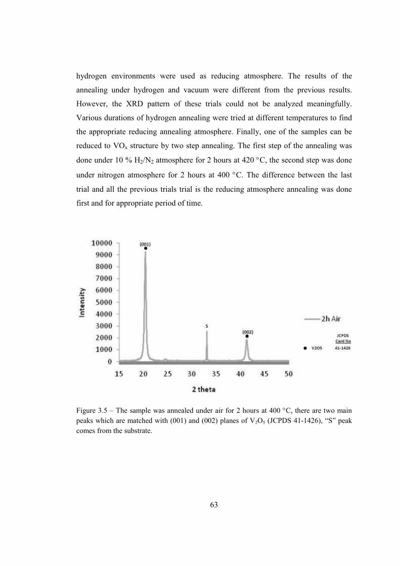
63
hydrogen environments were used as reducing atmosphere. The results of the
annealing under hydrogen and vacuum were different from the previous results.
However, the XRD pattern of these trials could not be analyzed meaningfully.
Various durations of hydrogen annealing were tried at different temperatures to find
the appropriate reducing annealing atmosphere. Finally, one of the samples can be
reduced to VOx structure by two step annealing. The first step of the annealing was
done under 10 % H2/N2 atmosphere for 2 hours at 420 °C, the second step was done
under nitrogen atmosphere for 2 hours at 400 °C. The difference between the last
trial and all the previous trials trial is the reducing atmosphere annealing was done
first and for appropriate period of time.
Figure 3.5 – The sample was annealed under air for 2 hours at 400 °C, there are two main
peaks which are matched with (001) and (002) planes of V2O5 (JCPDS 41-1426), “S” peak
comes from the substrate.
64
Figure 3.6 – The sample was annealed under nitrogen for 5 hours at 400 °C, there are two main peaks which are matched with (001) and (002) planes of V2O5 (JCPDS 41-1426), “S”
peak comes from the substrate.
Figure 3.7 – The sample was annealed firstly under air for 2 hours at 400 °C and then under nitrogen for 5 hours at 400 °C, there are two main peaks which are matched with (001) and
(002) planes of V2O5 (JCPDS 41-1426).
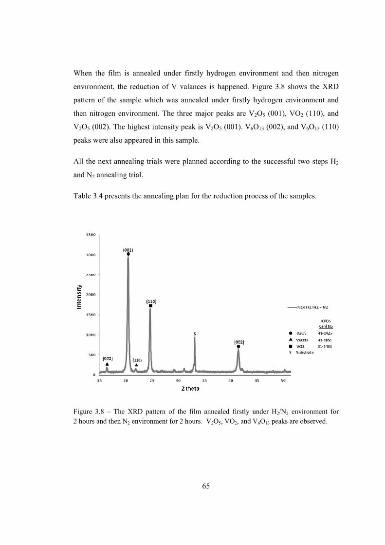
65
When the film is annealed under firstly hydrogen environment and then nitrogen
environment, the reduction of V valances is happened. Figure 3.8 shows the XRD
pattern of the sample which was annealed under firstly hydrogen environment and
then nitrogen environment. The three major peaks are V2O5 (001), VO2 (110), and
V2O5 (002). The highest intensity peak is V2O5 (001). V6O13 (002), and V6O13 (110)
peaks were also appeared in this sample.
All the next annealing trials were planned according to the successful two steps H2
and N2 annealing trial.
Table 3.4 presents the annealing plan for the reduction process of the samples.
Figure 3.8 – The XRD pattern of the film annealed firstly under H2/N2 environment for
2 hours and then N2 environment for 2 hours. V2O5, VO2, and V6O13 peaks are observed.
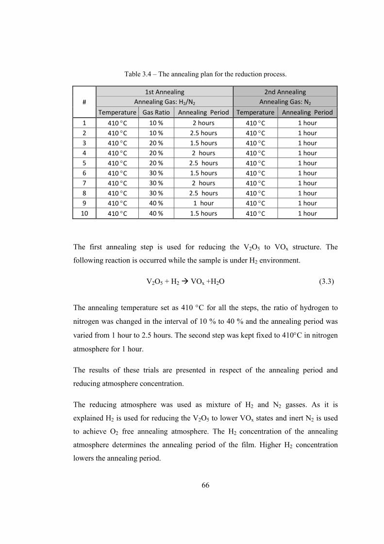
66
Table 3.4 – The annealing plan for the reduction process.
#
1st Annealing 2nd Annealing
Annealing Gas: H2/N2 Annealing Gas: N2
Temperature Gas Ratio Annealing Period Temperature Annealing Period
1 410 °C 10 % 2 hours 410 °C 1 hour
2 410 °C 10 % 2.5 hours 410 °C 1 hour
3 410 °C 20 % 1.5 hours 410 °C 1 hour
4 410 °C 20 % 2 hours 410 °C 1 hour
5 410 °C 20 % 2.5 hours 410 °C 1 hour
6 410 °C 30 % 1.5 hours 410 °C 1 hour
7 410 °C 30 % 2 hours 410 °C 1 hour
8 410 °C 30 % 2.5 hours 410 °C 1 hour
9 410 °C 40 % 1 hour 410 °C 1 hour
10 410 °C 40 % 1.5 hours 410 °C 1 hour
The first annealing step is used for reducing the V2O5 to VOx structure. The
following reaction is occurred while the sample is under H2 environment.
V2O5 + H2 VOx +H2O (3.3)
The annealing temperature set as 410 °C for all the steps, the ratio of hydrogen to
nitrogen was changed in the interval of 10 % to 40 % and the annealing period was
varied from 1 hour to 2.5 hours. The second step was kept fixed to 410°C in nitrogen
atmosphere for 1 hour.
The results of these trials are presented in respect of the annealing period and
reducing atmosphere concentration.
The reducing atmosphere was used as mixture of H2 and N2 gasses. As it is
explained H2 is used for reducing the V2O5 to lower VOx states and inert N2 is used
to achieve O2 free annealing atmosphere. The H2 concentration of the annealing
atmosphere determines the annealing period of the film. Higher H2 concentration
lowers the annealing period.
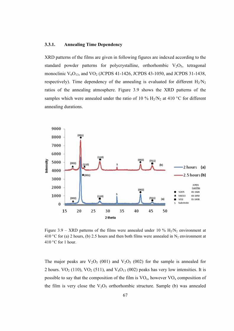
67
3.3.1. Annealing Time Dependency
XRD patterns of the films are given in following figures are indexed according to the
standard powder patterns for polycrystalline, orthorhombic V2O5, tetragonal
monoclinic V6O13, and VO2 (JCPDS 41-1426, JCPDS 43-1050, and JCPDS 31-1438,
respectively). Time dependency of the annealing is evaluated for different H2/N2
ratios of the annealing atmosphere. Figure 3.9 shows the XRD patterns of the
samples which were annealed under the ratio of 10 % H2/N2 at 410 °C for different
annealing durations.
(a)
(b)
Figure 3.9 – XRD patterns of the films were annealed under 10 % H2/N2 environment at
410 °C for (a) 2 hours, (b) 2.5 hours and then both films were annealed in N2 environment at
410 °C for 1 hour.
The major peaks are V2O5 (001) and V2O5 (002) for the sample is annealed for
2 hours. VO2 (110), VO2 (511), and V6O13 (002) peaks has very low intensities. It is
possible to say that the composition of the film is VOx, however VOx composition of
the film is very close the V2O5 orthorhombic structure. Sample (b) was annealed
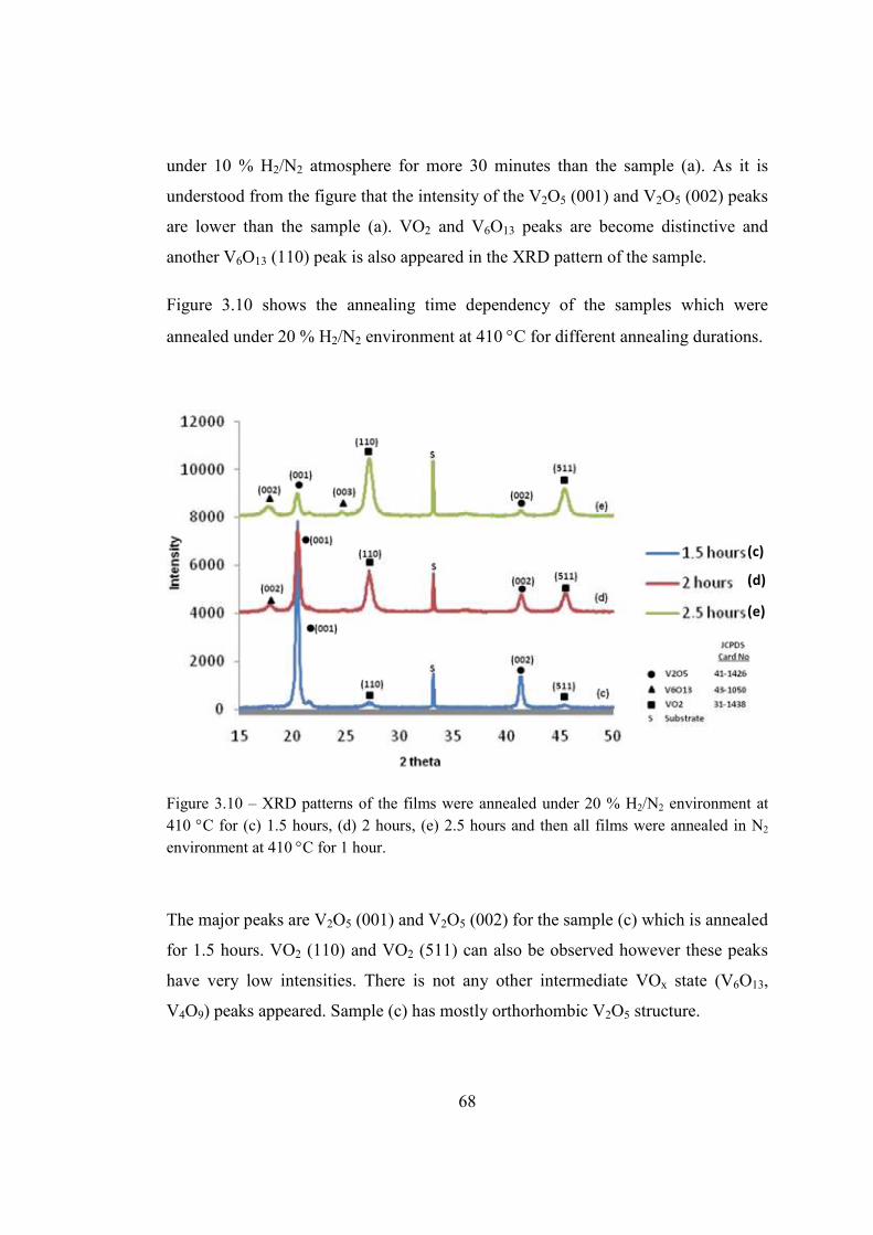
68
under 10 % H2/N2 atmosphere for more 30 minutes than the sample (a). As it is
understood from the figure that the intensity of the V2O5 (001) and V2O5 (002) peaks
are lower than the sample (a). VO2 and V6O13 peaks are become distinctive and
another V6O13 (110) peak is also appeared in the XRD pattern of the sample.
Figure 3.10 shows the annealing time dependency of the samples which were
annealed under 20 % H2/N2 environment at 410 °C for different annealing durations.
(c)
(d)
(e)
Figure 3.10 – XRD patterns of the films were annealed under 20 % H2/N2 environment at
410 °C for (c) 1.5 hours, (d) 2 hours, (e) 2.5 hours and then all films were annealed in N2
environment at 410 °C for 1 hour.
The major peaks are V2O5 (001) and V2O5 (002) for the sample (c) which is annealed
for 1.5 hours. VO2 (110) and VO2 (511) can also be observed however these peaks
have very low intensities. There is not any other intermediate VOx state (V6O13,
V4O9) peaks appeared. Sample (c) has mostly orthorhombic V2O5 structure.
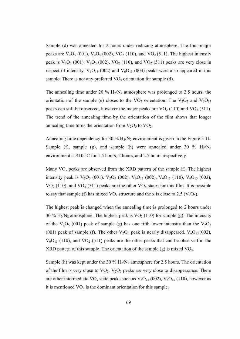
69
Sample (d) was annealed for 2 hours under reducing atmosphere. The four major
peaks are V2O5 (001), V2O5 (002), VO2 (110), and VO2 (511). The highest intensity
peak is V2O5 (001). V2O5 (002), VO2 (110), and VO2 (511) peaks are very close in
respect of intensity. V6O13 (002) and V6O13 (003) peaks were also appeared in this
sample. There is not any preferred VOx orientation for sample (d).
The annealing time under 20 % H2/N2 atmosphere was prolonged to 2.5 hours, the
orientation of the sample (e) closes to the VO2 orientation. The V2O5 and V6O13
peaks can still be observed, however the major peaks are VO2 (110) and VO2 (511).
The trend of the annealing time by the orientation of the film shows that longer
annealing time turns the orientation from V2O5 to VO2.
Annealing time dependency for 30 % H2/N2 environment is given in the Figure 3.11.
Sample (f), sample (g), and sample (h) were annealed under 30 % H2/N2
environment at 410 °C for 1.5 hours, 2 hours, and 2.5 hours respectively.
Many VOx peaks are observed from the XRD pattern of the sample (f). The highest
intensity peak is V2O5 (001). V2O5 (002), V6O13 (002), V6O13 (110), V6O13 (003),
VO2 (110), and VO2 (511) peaks are the other VOx states for this film. It is possible
to say that sample (f) has mixed VOx structure and the x is close to 2.5 (V2O5).
The highest peak is changed when the annealing time is prolonged to 2 hours under
30 % H2/N2 atmosphere. The highest peak is VO2 (110) for sample (g). The intensity
of the V2O5 (001) peak of sample (g) has one fifth lower intensity than the V2O5
(001) peak of sample (f). The other V2O5 peak is nearly disappeared. V6O13 (002),
V6O13 (110), and VO2 (511) peaks are the other peaks that can be observed in the
XRD pattern of this sample. The orientation of the sample (g) is mixed VOx.
Sample (h) was kept under the 30 % H2/N2 atmosphere for 2.5 hours. The orientation
of the film is very close to VO2. V2O5 peaks are very close to disappearance. There
are other intermediate VOx state peaks such as V6O13 (002), V6O13 (110), however as
it is mentioned VO2 is the dominant orientation for this sample.
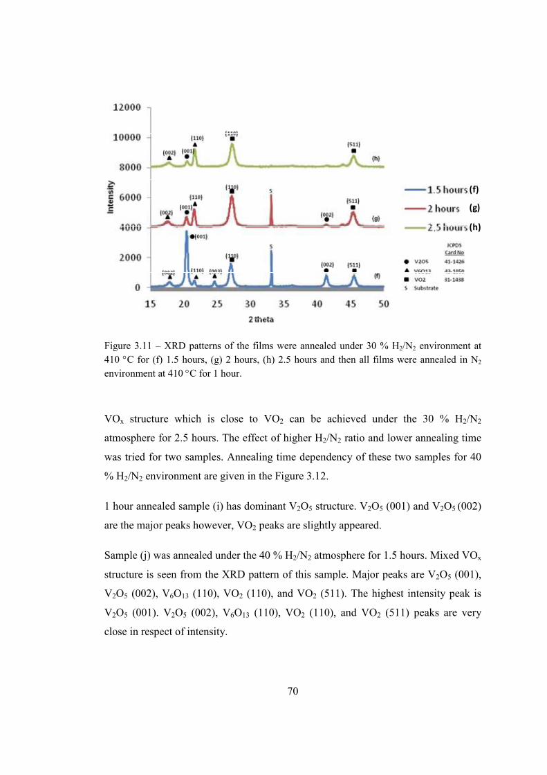
70
(f)
(g)
(h)
Figure 3.11 – XRD patterns of the films were annealed under 30 % H2/N2 environment at
410 °C for (f) 1.5 hours, (g) 2 hours, (h) 2.5 hours and then all films were annealed in N2
environment at 410 °C for 1 hour.
VOx structure which is close to VO2 can be achieved under the 30 % H2/N2
atmosphere for 2.5 hours. The effect of higher H2/N2 ratio and lower annealing time
was tried for two samples. Annealing time dependency of these two samples for 40
% H2/N2 environment are given in the Figure 3.12.
1 hour annealed sample (i) has dominant V2O5 structure. V2O5 (001) and V2O5 (002)
are the major peaks however, VO2 peaks are slightly appeared.
Sample (j) was annealed under the 40 % H2/N2 atmosphere for 1.5 hours. Mixed VOx
structure is seen from the XRD pattern of this sample. Major peaks are V2O5 (001),
V2O5 (002), V6O13 (110), VO2 (110), and VO2 (511). The highest intensity peak is
V2O5 (001). V2O5 (002), V6O13 (110), VO2 (110), and VO2 (511) peaks are very
close in respect of intensity.
71
(i)
(j)
Figure 3.12 – XRD patterns of the films were annealed under 40 % H2/N2 environment at
410 °C for (f) 1.5 hours, (g) 2 hours, (h) 2.5 hours and then all films were annealed in N2
environment at 410 °C for 1 hour.
It is understood from the analysis of the XRD patterns of the films that annealed for
different time periods at same environment; the film structure closes from V2O5 to
VO2 when the annealing periods prolongs. Intermediate oxygen states of VOx are
also observed between the V2O5 and VO2.
3.3.2. H2 Concentration Dependency
The same XRD patterns of the samples are presented in respect to the hydrogen
concentration of the annealing environment. XRD patterns of the samples which
were annealed for same period of time but in different H2/N2 ratios environments are
evaluated to see the effect of the reducing gas mixture.
Figure 3.13 shows the XRD patterns of three samples which were annealed for
1.5 hours in different H2/N2 concentration environments.
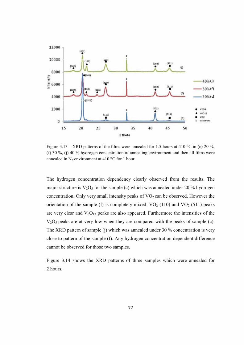
72
(j)
(f)
(c)
Figure 3.13 – XRD patterns of the films were annealed for 1.5 hours at 410 °C in (c) 20 %,
(f) 30 %, (j) 40 % hydrogen concentration of annealing environment and then all films were
annealed in N2 environment at 410 °C for 1 hour.
The hydrogen concentration dependency clearly observed from the results. The
major structure is V2O5 for the sample (c) which was annealed under 20 % hydrogen
concentration. Only very small intensity peaks of VO2 can be observed. However the
orientation of the sample (f) is completely mixed. VO2 (110) and VO2 (511) peaks
are very clear and V6O13 peaks are also appeared. Furthermore the intensities of the
V2O5 peaks are at very low when they are compared with the peaks of sample (c).
The XRD pattern of sample (j) which was annealed under 30 % concentration is very
close to pattern of the sample (f). Any hydrogen concentration dependent difference
cannot be observed for those two samples.
Figure 3.14 shows the XRD patterns of three samples which were annealed for
2 hours.
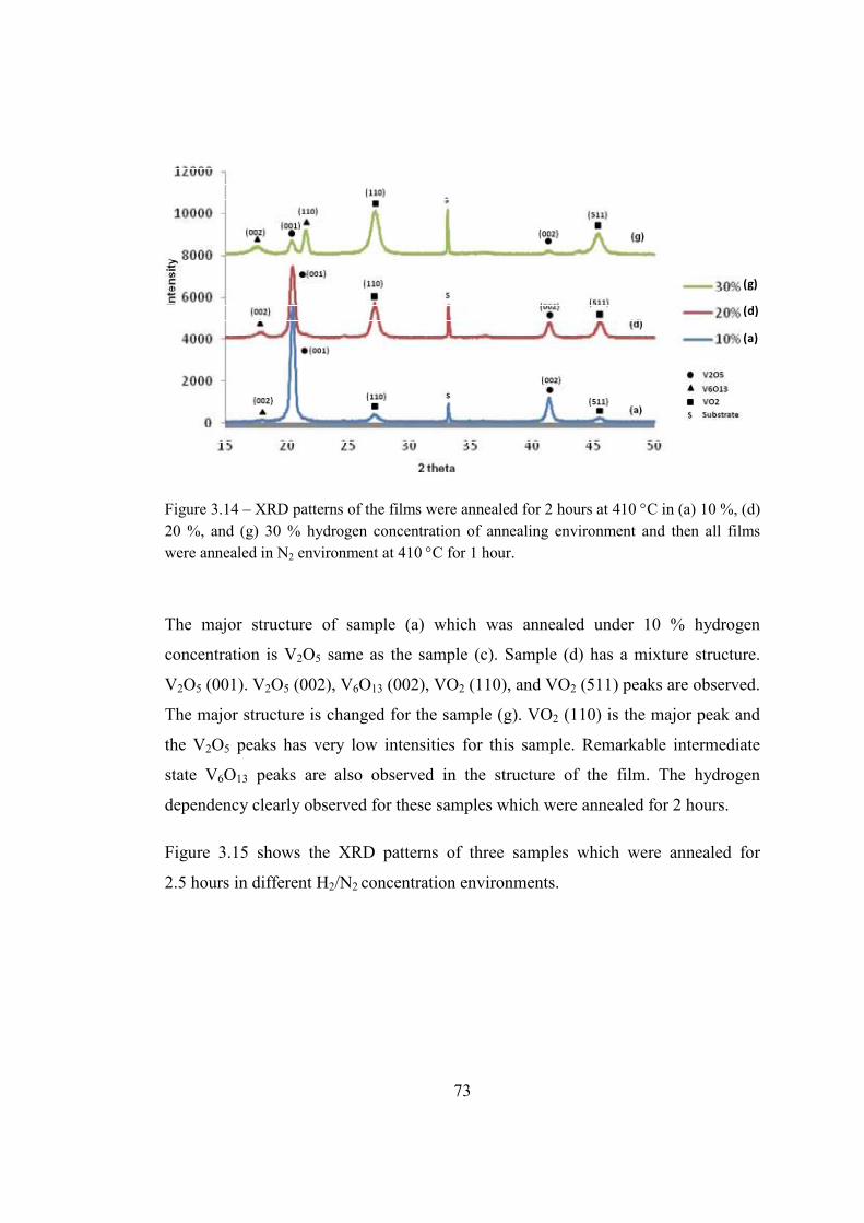
73
(g)
(d)
(a)
Figure 3.14 – XRD patterns of the films were annealed for 2 hours at 410 °C in (a) 10 %, (d)
20 %, and (g) 30 % hydrogen concentration of annealing environment and then all films
were annealed in N2 environment at 410 °C for 1 hour.
The major structure of sample (a) which was annealed under 10 % hydrogen
concentration is V2O5 same as the sample (c). Sample (d) has a mixture structure.
V2O5 (001). V2O5 (002), V6O13 (002), VO2 (110), and VO2 (511) peaks are observed.
The major structure is changed for the sample (g). VO2 (110) is the major peak and
the V2O5 peaks has very low intensities for this sample. Remarkable intermediate
state V6O13 peaks are also observed in the structure of the film. The hydrogen
dependency clearly observed for these samples which were annealed for 2 hours.
Figure 3.15 shows the XRD patterns of three samples which were annealed for
2.5 hours in different H2/N2 concentration environments.
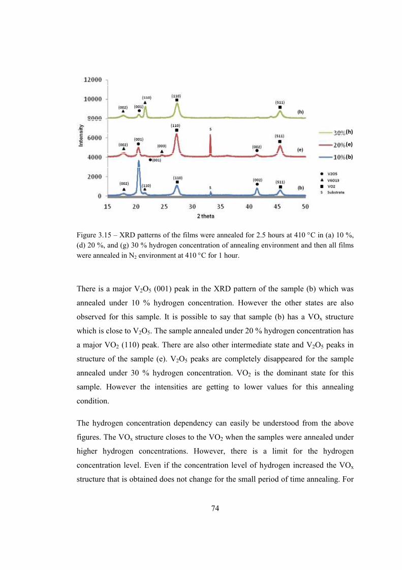
74
(h)
(e)
(b)
Figure 3.15 – XRD patterns of the films were annealed for 2.5 hours at 410 °C in (a) 10 %,
(d) 20 %, and (g) 30 % hydrogen concentration of annealing environment and then all films
were annealed in N2 environment at 410 °C for 1 hour.
There is a major V2O5 (001) peak in the XRD pattern of the sample (b) which was
annealed under 10 % hydrogen concentration. However the other states are also
observed for this sample. It is possible to say that sample (b) has a VOx structure
which is close to V2O5. The sample annealed under 20 % hydrogen concentration has
a major VO2 (110) peak. There are also other intermediate state and V2O5 peaks in
structure of the sample (e). V2O5 peaks are completely disappeared for the sample
annealed under 30 % hydrogen concentration. VO2 is the dominant state for this
sample. However the intensities are getting to lower values for this annealing
condition.
The hydrogen concentration dependency can easily be understood from the above
figures. The VOx structure closes to the VO2 when the samples were annealed under
higher hydrogen concentrations. However, there is a limit for the hydrogen
concentration level. Even if the concentration level of hydrogen increased the VOx
structure that is obtained does not change for the small period of time annealing. For
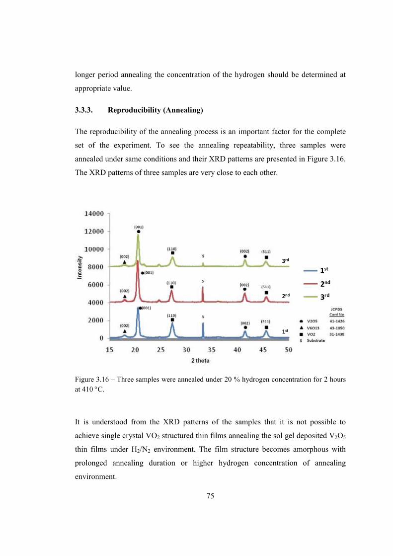
75
longer period annealing the concentration of the hydrogen should be determined at
appropriate value.
3.3.3. Reproducibility (Annealing)
The reproducibility of the annealing process is an important factor for the complete
set of the experiment. To see the annealing repeatability, three samples were
annealed under same conditions and their XRD patterns are presented in Figure 3.16.
The XRD patterns of three samples are very close to each other.
1st
2nd
3rd
1st
2nd
3rd
Figure 3.16 – Three samples were annealed under 20 % hydrogen concentration for 2 hours
at 410 °C.
It is understood from the XRD patterns of the samples that it is not possible to
achieve single crystal VO2 structured thin films annealing the sol gel deposited V2O5
thin films under H2/N2 environment. The film structure becomes amorphous with
prolonged annealing duration or higher hydrogen concentration of annealing
environment.
76
CHAPTER 4
PERFORMANCE OF SOL-GEL DEPOSITED VOx THIN
FILMS
This chapter presents the performance of the sol-gel growth VOx thin films.
Section 4.1 defines the methods and procedures of sheet resistance, Temperature
Coefficient of Resistance (TCR), and noise measurements. Section 4.2 gives the
results of the measurements.
4.1. Measurement Methods
4.1.1. Sheet Resistance Measurement Method
The sheet resistance values of the thin films give an opinion about the relation
between the VOx structure and the sheet resistance. The sheet resistances of the thin
films were measured with four point probe technique. In this study Signatone
QaudPro Automatic System was used for four point probe measurements. Figure 4.1
shows the four point probe measurement system.
Basic working principle of a four-point probe is measuring sheet resistance of a thin
film on an insulating substrate. If the surface does not an insulator the sheet
resistance cannot be measured. In this study, sheet resistances of thin films that were
coated on SiNx substrates were measured by four point probe.
There are two probes which are connected a current supply are placed outer side of
all dour point probes. The other two probes measure the voltage between two probes.
When the current applied, the voltage change is read from the inner probes. Figure
4.2 and Figure 4.3 show the probe structure of the measurement system. The
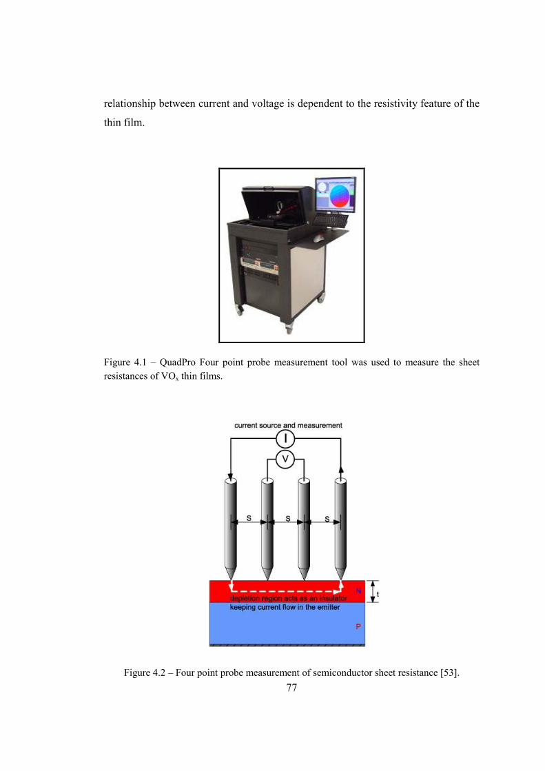
77
relationship between current and voltage is dependent to the resistivity feature of the
thin film.
Figure 4.1 – QuadPro Four point probe measurement tool was used to measure the sheet
resistances of VOx thin films.
Figure 4.2 – Four point probe measurement of semiconductor sheet resistance [53].
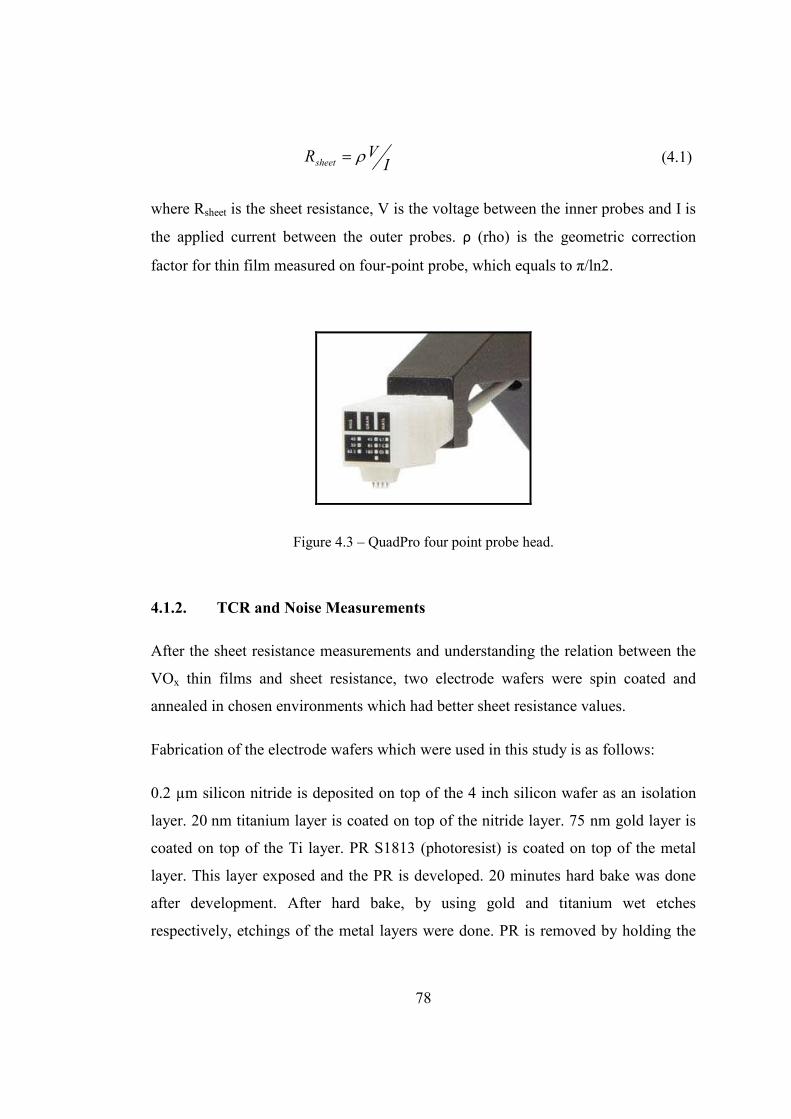
78
IVRsheet ρ= (4.1)
where Rsheet is the sheet resistance, V is the voltage between the inner probes and I is
the applied current between the outer probes. ρ (rho) is the geometric correction
factor for thin film measured on four-point probe, which equals to π/ln2.
Figure 4.3 – QuadPro four point probe head.
4.1.2. TCR and Noise Measurements
After the sheet resistance measurements and understanding the relation between the
VOx thin films and sheet resistance, two electrode wafers were spin coated and
annealed in chosen environments which had better sheet resistance values.
Fabrication of the electrode wafers which were used in this study is as follows:
0.2 µm silicon nitride is deposited on top of the 4 inch silicon wafer as an isolation
layer. 20 nm titanium layer is coated on top of the nitride layer. 75 nm gold layer is
coated on top of the Ti layer. PR S1813 (photoresist) is coated on top of the metal
layer. This layer exposed and the PR is developed. 20 minutes hard bake was done
after development. After hard bake, by using gold and titanium wet etches
respectively, etchings of the metal layers were done. PR is removed by holding the
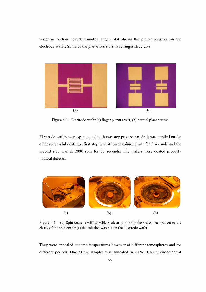
79
wafer in acetone for 20 minutes. Figure 4.4 shows the planar resistors on the
electrode wafer. Some of the planar resistors have finger structures.
(a) (b)
Figure 4.4 – Electrode wafer (a) finger planar resist, (b) normal planar resist.
Electrode wafers were spin coated with two step processing. As it was applied on the
other successful coatings, first step was at lower spinning rate for 5 seconds and the
second step was at 2000 rpm for 75 seconds. The wafers were coated properly
without defects.
(a) (b) (c)
Figure 4.5 – (a) Spin coater (METU-MEMS clean room) (b) the wafer was put on to the
chuck of the spin coater (c) the solution was put on the electrode wafer.
They were annealed at same temperatures however at different atmospheres and for
different periods. One of the samples was annealed in 20 % H2N2 environment at
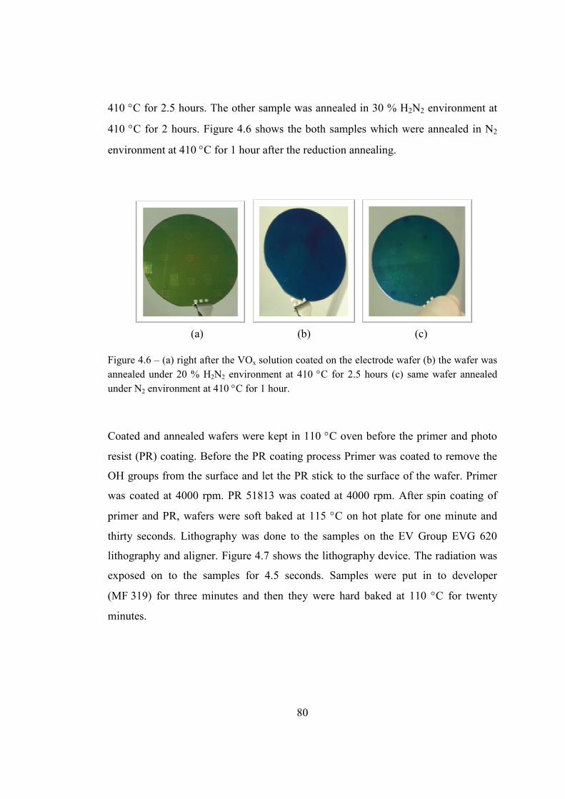
80
410 °C for 2.5 hours. The other sample was annealed in 30 % H2N2 environment at
410 °C for 2 hours. Figure 4.6 shows the both samples which were annealed in N2
environment at 410 °C for 1 hour after the reduction annealing.
(a) (b) (c)
Figure 4.6 – (a) right after the VOx solution coated on the electrode wafer (b) the wafer was
annealed under 20 % H2N2 environment at 410 °C for 2.5 hours (c) same wafer annealed
under N2 environment at 410 °C for 1 hour.
Coated and annealed wafers were kept in 110 °C oven before the primer and photo
resist (PR) coating. Before the PR coating process Primer was coated to remove the
OH groups from the surface and let the PR stick to the surface of the wafer. Primer
was coated at 4000 rpm. PR 51813 was coated at 4000 rpm. After spin coating of
primer and PR, wafers were soft baked at 115 °C on hot plate for one minute and
thirty seconds. Lithography was done to the samples on the EV Group EVG 620
lithography and aligner. Figure 4.7 shows the lithography device. The radiation was
exposed on to the samples for 4.5 seconds. Samples were put in to developer
(MF 319) for three minutes and then they were hard baked at 110 °C for twenty
minutes.
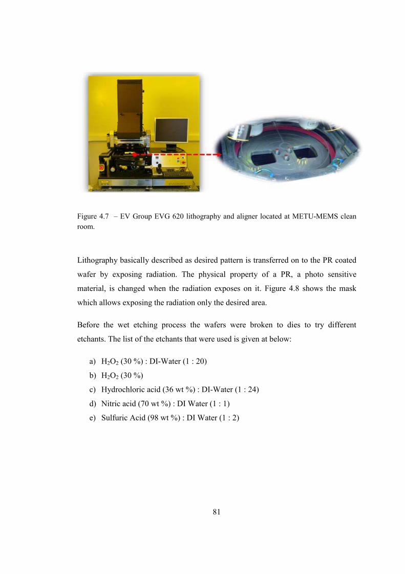
81
Figure 4.7 – EV Group EVG 620 lithography and aligner located at METU-MEMS clean
room.
Lithography basically described as desired pattern is transferred on to the PR coated
wafer by exposing radiation. The physical property of a PR, a photo sensitive
material, is changed when the radiation exposes on it. Figure 4.8 shows the mask
which allows exposing the radiation only the desired area.
Before the wet etching process the wafers were broken to dies to try different
etchants. The list of the etchants that were used is given at below:
a) H2O2 (30 %) : DI-Water (1 : 20)
b) H2O2 (30 %)
c) Hydrochloric acid (36 wt %) : DI-Water (1 : 24)
d) Nitric acid (70 wt %) : DI Water (1 : 1)
e) Sulfuric Acid (98 wt %) : DI Water (1 : 2)
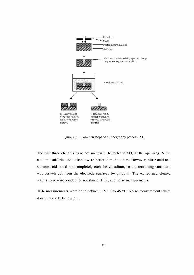
82
Figure 4.8 – Common steps of a lithography process [54].
The first three etchants were not successful to etch the VOx at the openings. Nitric
acid and sulfuric acid etchants were better than the others. However, nitric acid and
sulfuric acid could not completely etch the vanadium, so the remaining vanadium
was scratch out from the electrode surfaces by pinpoint. The etched and cleared
wafers were wire bonded for resistance, TCR, and noise measurements.
TCR measurements were done between 15 °C to 45 °C. Noise measurements were
done in 27 kHz bandwidth.
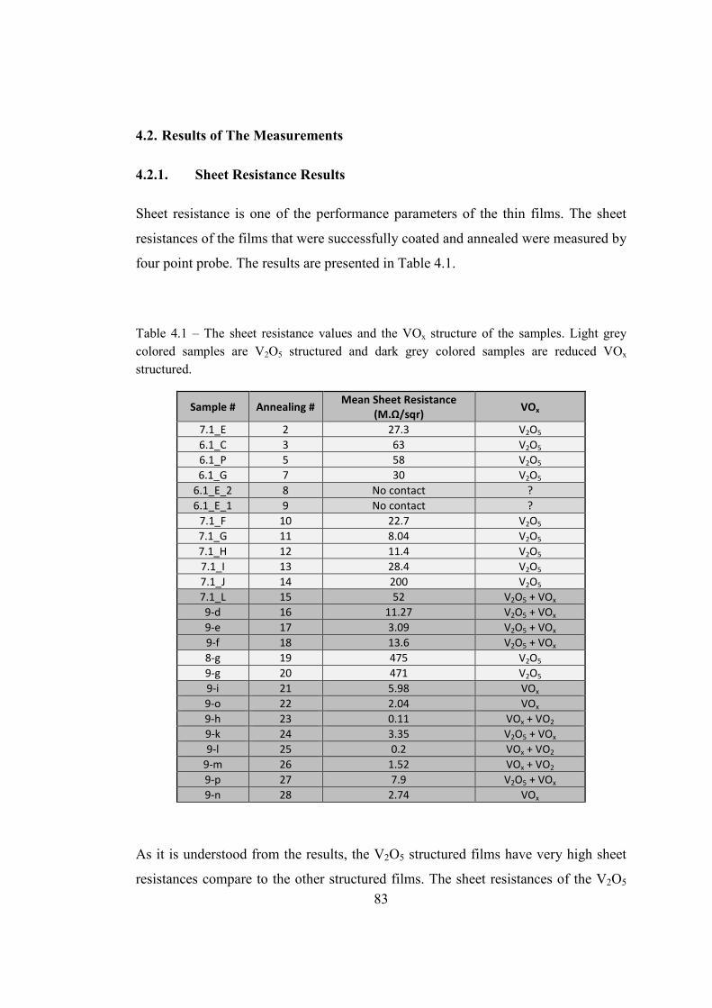
83
4.2. Results of The Measurements
4.2.1. Sheet Resistance Results
Sheet resistance is one of the performance parameters of the thin films. The sheet
resistances of the films that were successfully coated and annealed were measured by
four point probe. The results are presented in Table 4.1.
Table 4.1 – The sheet resistance values and the VOx structure of the samples. Light grey
colored samples are V2O5 structured and dark grey colored samples are reduced VOx
structured.
Sample # Annealing # Mean Sheet Resistance
(M.Ω/sqr) VOx
7.1_E 2 27.3 V2O5
6.1_C 3 63 V2O5
6.1_P 5 58 V2O5
6.1_G 7 30 V2O5
6.1_E_2 8 No contact ?
6.1_E_1 9 No contact ?
7.1_F 10 22.7 V2O5
7.1_G 11 8.04 V2O5
7.1_H 12 11.4 V2O5 7.1_I 13 28.4 V2O5 7.1_J 14 200 V2O5 7.1_L 15 52 V2O5 + VOx
9-d 16 11.27 V2O5 + VOx 9-e 17 3.09 V2O5 + VOx 9-f 18 13.6 V2O5 + VOx 8-g 19 475 V2O5 9-g 20 471 V2O5 9-i 21 5.98 VOx
9-o 22 2.04 VOx
9-h 23 0.11 VOx + VO2
9-k 24 3.35 V2O5 + VOx
9-l 25 0.2 VOx + VO2
9-m 26 1.52 VOx + VO2
9-p 27 7.9 V2O5 + VOx
9-n 28 2.74 VOx
As it is understood from the results, the V2O5 structured films have very high sheet
resistances compare to the other structured films. The sheet resistances of the V2O5
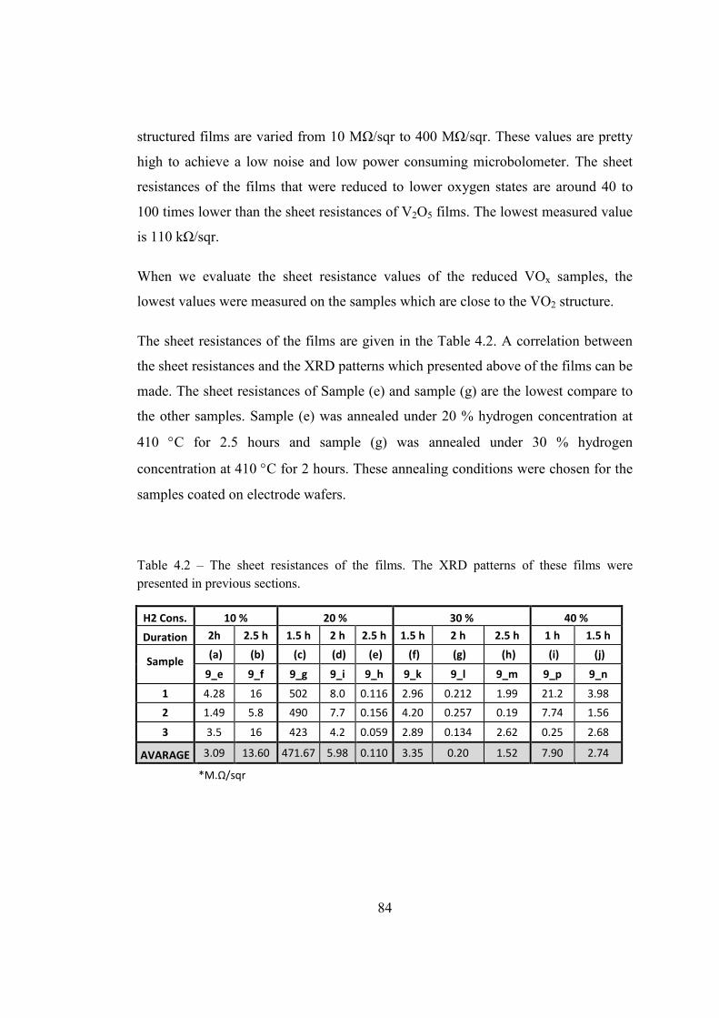
84
structured films are varied from 10 MΩ/sqr to 400 MΩ/sqr. These values are pretty
high to achieve a low noise and low power consuming microbolometer. The sheet
resistances of the films that were reduced to lower oxygen states are around 40 to
100 times lower than the sheet resistances of V2O5 films. The lowest measured value
is 110 kΩ/sqr.
When we evaluate the sheet resistance values of the reduced VOx samples, the
lowest values were measured on the samples which are close to the VO2 structure.
The sheet resistances of the films are given in the Table 4.2. A correlation between
the sheet resistances and the XRD patterns which presented above of the films can be
made. The sheet resistances of Sample (e) and sample (g) are the lowest compare to
the other samples. Sample (e) was annealed under 20 % hydrogen concentration at
410 °C for 2.5 hours and sample (g) was annealed under 30 % hydrogen
concentration at 410 °C for 2 hours. These annealing conditions were chosen for the
samples coated on electrode wafers.
Table 4.2 – The sheet resistances of the films. The XRD patterns of these films were
presented in previous sections.
H2 Cons. 10 % 20 % 30 % 40 %
Duration 2h 2.5 h 1.5 h 2 h 2.5 h 1.5 h 2 h 2.5 h 1 h 1.5 h
Sample
(a) (b) (c) (d) (e) (f) (g) (h) (i) (j)
9_e 9_f 9_g 9_i 9_h 9_k 9_l 9_m 9_p 9_n
1 4.28 16 502 8.0 0.116 2.96 0.212 1.99 21.2 3.98
2 1.49 5.8 490 7.7 0.156 4.20 0.257 0.19 7.74 1.56
3 3.5 16 423 4.2 0.059 2.89 0.134 2.62 0.25 2.68
AVARAGE 3.09 13.60 471.67 5.98 0.110 3.35 0.20 1.52 7.90 2.74
*M.Ω/sqr
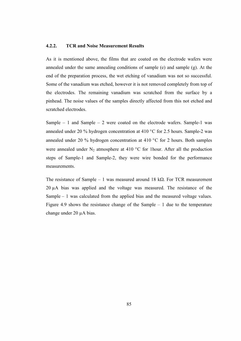
85
4.2.2. TCR and Noise Measurement Results
As it is mentioned above, the films that are coated on the electrode wafers were
annealed under the same annealing conditions of sample (e) and sample (g). At the
end of the preparation process, the wet etching of vanadium was not so successful.
Some of the vanadium was etched, however it is not removed completely from top of
the electrodes. The remaining vanadium was scratched from the surface by a
pinhead. The noise values of the samples directly affected from this not etched and
scratched electrodes.
Sample – 1 and Sample – 2 were coated on the electrode wafers. Sample-1 was
annealed under 20 % hydrogen concentration at 410 °C for 2.5 hours. Sample-2 was
annealed under 20 % hydrogen concentration at 410 °C for 2 hours. Both samples
were annealed under N2 atmosphere at 410 °C for 1hour. After all the production
steps of Sample-1 and Sample-2, they were wire bonded for the performance
measurements.
The resistance of Sample – 1 was measured around 18 kΩ. For TCR measurement
20 µA bias was applied and the voltage was measured. The resistance of the
Sample – 1 was calculated from the applied bias and the measured voltage values.
Figure 4.9 shows the resistance change of the Sample – 1 due to the temperature
change under 20 µA bias.
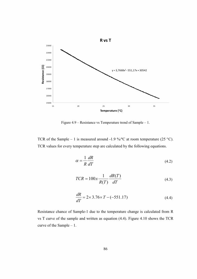
86
y = 3,7668x2 - 551,17x + 30542
15000
16000
17000
18000
19000
20000
21000
22000
23000
15 20 25 30 35
Re
sist
an
ce (Ω
)
Temperature (ºC)
R vs T
Figure 4.9 – Resistance vs Temperature trend of Sample – 1.
TCR of the Sample – 1 is measured around -1.9 %/ºC at room temperature (25 °C).
TCR values for every temperature step are calculated by the following equations.
dT
dR
R
1=α (4.2)
dT
TdR
TRxTCR
)(
)(
1100= (4.3)
)17.551(76.32 −−××= TdT
dR (4.4)
Resistance chance of Sample-1 due to the temperature change is calculated from R
vs T curve of the sample and written as equation (4.4). Figure 4.10 shows the TCR
curve of the Sample – 1.
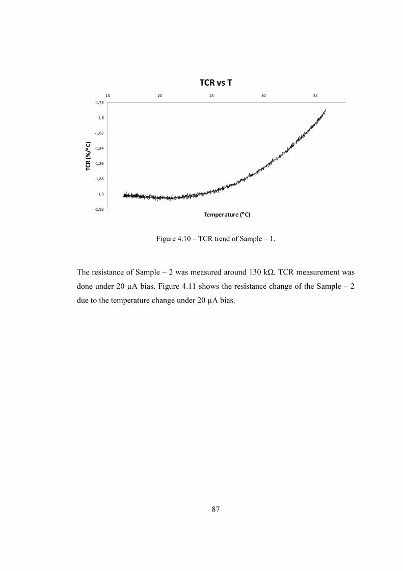
87
-1,92
-1,9
-1,88
-1,86
-1,84
-1,82
-1,8
-1,78
15 20 25 30 35
TC
R (
%/ °° °°
C)
Temperature (°°°°C)
TCR vs T
Figure 4.10 – TCR trend of Sample – 1.
The resistance of Sample – 2 was measured around 130 kΩ. TCR measurement was
done under 20 µA bias. Figure 4.11 shows the resistance change of the Sample – 2
due to the temperature change under 20 µA bias.
88
y = 25,267x2 - 3807,2x + 213045
R² = 0,9998
130000
135000
140000
145000
150000
155000
160000
165000
13 15 17 19 21 23 25 27
Re
sist
an
ce (Ω
)
Temperature (ºC)
R vs T
Figure 4.11 – Resistance vs Temperature trend of Sample – 2.
TCR of the Sample – 2 is measured around -1.87 %/ºC at room temperature (25 ºC).
TCR values for every temperature step are calculated by the following equations.
)2.3807(27.252 −−××= TdT
dR (4.5)
Resistance chance of Sample – 2 due to the temperature change is calculated from R
vs T curve of the sample and written as equation (4.5). Figure 4.12 shows the TCR
curve of the Sample – 2.
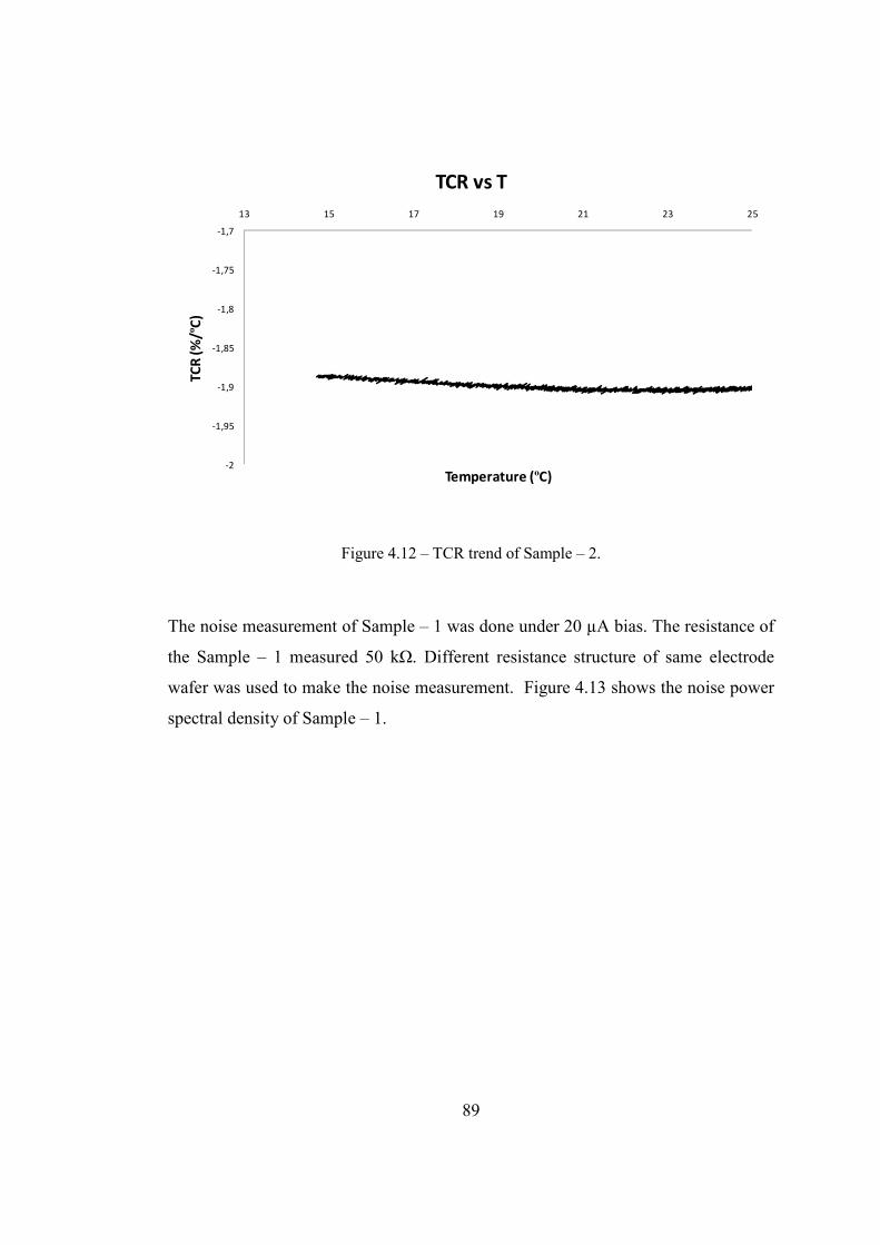
89
-2
-1,95
-1,9
-1,85
-1,8
-1,75
-1,7
13 15 17 19 21 23 25
TC
R (
%/º
C)
Temperature (ºC)
TCR vs T
Figure 4.12 – TCR trend of Sample – 2.
The noise measurement of Sample – 1 was done under 20 µA bias. The resistance of
the Sample – 1 measured 50 kΩ. Different resistance structure of same electrode
wafer was used to make the noise measurement. Figure 4.13 shows the noise power
spectral density of Sample – 1.
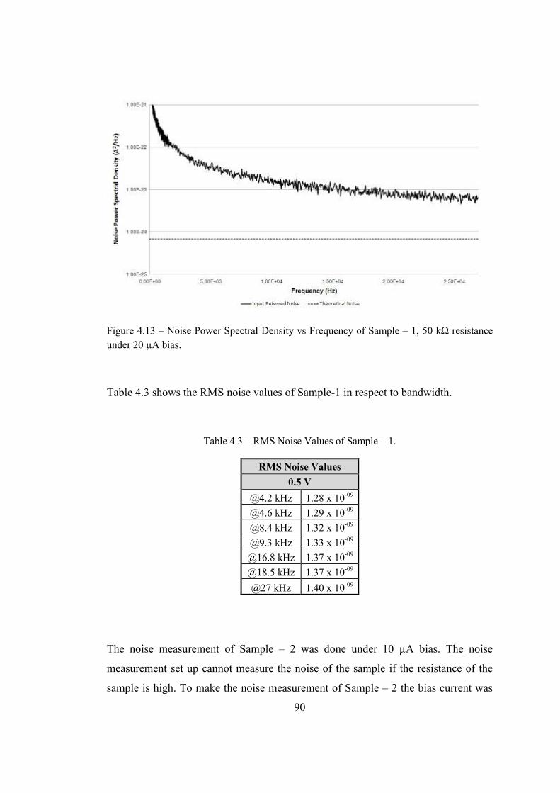
90
Figure 4.13 – Noise Power Spectral Density vs Frequency of Sample – 1, 50 kΩ resistance
under 20 µA bias.
Table 4.3 shows the RMS noise values of Sample-1 in respect to bandwidth.
Table 4.3 – RMS Noise Values of Sample – 1.
RMS Noise Values
0.5 V
@4.2 kHz 1.28 x 10-09
@4.6 kHz 1.29 x 10-09
@8.4 kHz 1.32 x 10-09
@9.3 kHz 1.33 x 10-09
@16.8 kHz 1.37 x 10-09
@18.5 kHz 1.37 x 10-09
@27 kHz 1.40 x 10-09
The noise measurement of Sample – 2 was done under 10 µA bias. The noise
measurement set up cannot measure the noise of the sample if the resistance of the
sample is high. To make the noise measurement of Sample – 2 the bias current was
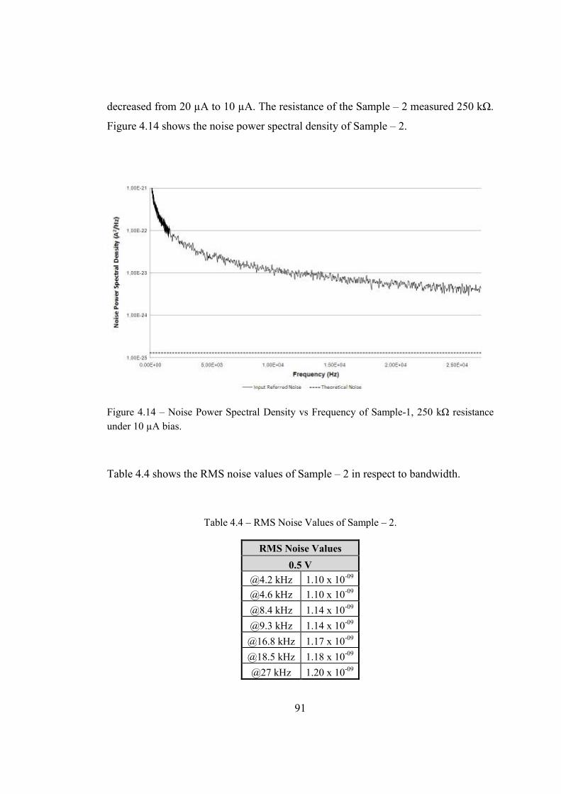
91
decreased from 20 µA to 10 µA. The resistance of the Sample – 2 measured 250 kΩ.
Figure 4.14 shows the noise power spectral density of Sample – 2.
Figure 4.14 – Noise Power Spectral Density vs Frequency of Sample-1, 250 kΩ resistance
under 10 µA bias.
Table 4.4 shows the RMS noise values of Sample – 2 in respect to bandwidth.
Table 4.4 – RMS Noise Values of Sample – 2.
RMS Noise Values
0.5 V
@4.2 kHz 1.10 x 10-09
@4.6 kHz 1.10 x 10-09
@8.4 kHz 1.14 x 10-09
@9.3 kHz 1.14 x 10-09
@16.8 kHz 1.17 x 10-09
@18.5 kHz 1.18 x 10-09
@27 kHz 1.20 x 10-09
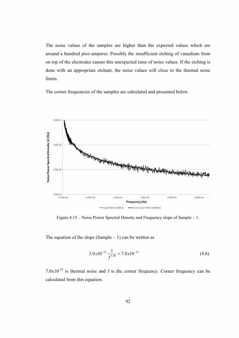
92
The noise values of the samples are higher than the expected values which are
around a hundred pico-amperes. Possibly the insufficient etching of vanadium from
on top of the electrodes causes this unexpected raise of noise values. If the etching is
done with an appropriate etchant, the noise values will close to the thermal noise
limits.
The corner frequencies of the samples are calculated and presented below.
Figure 4.15 – Noise Power Spectral Density and Frequency slope of Sample – 1.
The equation of the slope (Sample – 1) can be written as
25
09.1
19 100.71
109.3 −− + xf
x (4.6)
7.0x10⁻²⁵ is thermal noise and f is the corner frequency. Corner frequency can be
calculated from this equation.
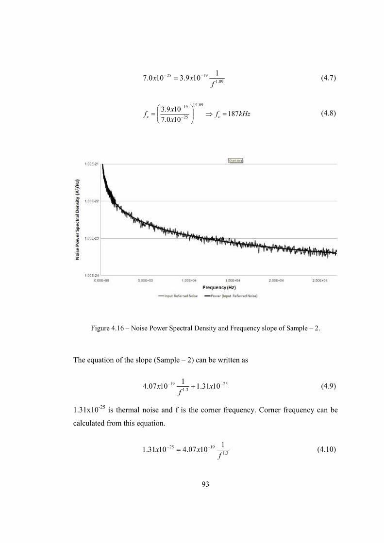
93
09.1
1925 1109.3100.7
fxx
−− = (4.7)
kHzfx
xf cc 187
100.7
109.309.11
25
19
=⇒
=
−
−
(4.8)
Figure 4.16 – Noise Power Spectral Density and Frequency slope of Sample – 2.
The equation of the slope (Sample – 2) can be written as
25
3.1
19 1031.11
1007.4 −− + xf
x (4.9)
1.31x10⁻²⁵ is thermal noise and f is the corner frequency. Corner frequency can be
calculated from this equation.
3.1
1925 11007.41031.1
fxx
−− = (4.10)
94
MHzfx
xf cc 04.4
1031.1
1007.43.11
25
19
=⇒
=
−
−
(4.11)
The performance critique characteristics of the thin films were measured. The sheet
resistance, resistance, and TCR values of the thin films were promising for using the
films in a microbolometer application. However, the noise values are pretty high, but
they can be improved by using appropriate etchant to remove the VOx from on top
of the electrodes. The following chapter presents the conclusions of the whole study,
and discusses the future work to improve the results.
95
CHAPTER 5
CONCLUSIONS
This chapter presents the main results obtained from this study. Sol-gel VOx coating
solutions were formed by mixing DI water and solid vanadium material which is a
solid product of dissolution of hydrogen proxide and vanadium metal powder. The
solution was spin coated on Si and SiNx wafers. Process conditions and especially
annealing step play the key roles in maintaining the desired film quality. Annealing
environment and annealing period were the main variables of this study. Reducing
annealing was done with hydrogen and the concentration of the hydrogen was
changed between 10 % and 40 %. The annealing period was varied between 1 hour
and 2.5 hours in the reducing atmosphere. Specific findings related to film
formation, performance parameters will be summarized as follows:
• Solution preparation and coating parameters: Appropriate formulation of the
solution is a must for uniform, homogeneous and defect free coatings. The mixing
ratio of 1 g : 100 ml vanadium powder and hydrogen peroxide has been found to be
the most suitable for the purpose of preparing solid vanadium material. The mixing
ratio of solid material and DI water have been determined as 1 g : 33 ml respectively.
The viscosities of the solutions prepared with described ratios are 5.77±3. The
spinning process has two stages which are slower one and the faster one. Spinning
rates of the best coating are 500 rpm for 5 seconds and 2000 rpm for 75 seconds. The
average thicknesses for the thin films that coated with mentioned spinning process
are about 30±3 nm. The films homogenously covered on the surface of Si and SiNx
substrates.
96
• Effect of annealing environment and annealing duration: The annealing of
successfully coated wafers was done in two steps. The first step was done at 410 °C
under hydrogen environment providing a reducing atmosphere. Different hydrogen
concentrations of reducing annealing were done. XRD results have revealed that the
higher hydrogen concentration provide more reducing VOx molecules. Similarly, if
the annealing duration prolonged, the reduced molecule amount is increased.
However there is a limit both for concentration of hydrogen and annealing period.
Even if the hydrogen concentration increases, the reduction does not start before 1
hour annealing. If the annealing time prolonged more than a value, the crystal
structure of the film starts to disappear. The second step of the annealing was done
under nitrogen environment at 410 °C for 2 hours. The conditions of the second
annealing step were fixed for all trials.
The best reductions were achieved with two different annealing conditions. The first
one is under 20 % H2/N2 environment at 410 °C for 2.5 hours. The other one is under
30 % H2/N2 environment at 410 °C for 2 hours. When the XRD patterns of the films
that annealed with these two annealing conditions they show similarities. The
highest peak is VO2 (110). The intensity of the V2O5 (001) peak which is the highest
peak before reduction is lowered. The other V2O5 peaks are nearly disappeared.
V6O13 (002), V6O13 (110), and VO2 (511) peaks are the other peaks that can be
observed in the XRD pattern of these samples. The orientation of these samples is
mixed VOx. The samples annealed by these conditions give the lowest sheet
resistance values. Their sheet resistances are in the range of 100 kΩ/sqr – 200
kΩ/sqr.
Two electrode wafers were coated and annealed under the conditions that are
described above. Resistance, TCR, and noise measurements were done to see the
performance of the thin films. The resistances are 18 kΩ and 130 kΩ under 20 µA
bias. The TCR values of the samples measured around -1.9 %/°C at room
temperature (25 °C). The noise values were a little bit higher than expected. There
are many things that directly affect the noise. The etching of vanadium from on top
97
of the electrodes is inadequate. This may cause the undesired raise in the noise. The
corner frequencies are 187 kHz and 4.04 MHz.
From the results it can be concluded that, it is possible obtain mixed VOx thin film
by using appropriate sol preparation processes and annealing conditions. The
resistance values of such VOx structured films are lower than V2O5 structured thin
films. The TCR values of these films are high enough to use in a microbolometer
application. However, the etching process which is used to remove the excess VOx
layer from on top of the electrodes should be developed to achieve lower noise
values.
98
REFERENCES
[1] F. Niklaus, “MEMS-Based Uncooled Infrared Bolometer Arrays – A Review,”
MEMS/MOEMS Technologies and Applications III, edited by J. C. Chiao, X.
Chen, Z. Zhou, and Xinxin Li, SPIE, vol. 6836, pp. 1-5, 2007.
[2] R. B. Darling and S. Iwanaga, “Structure, properties, and MEMS and
microelectronic applications of vanadium oxides,” Sadhana, vol. 34, part. 4,
pp. 531-542, 2009.
[3] J. Nag and R. F. Haglund, “Synthesis of Vanadium dioxide thin films and
nanoparticles,” Journal of Physics Condensed Matter, vol. 20, pp. 1-14, 2008.
[4] J. Livage and D. Ganguli, “Sol-gel electrochromic coatings and devices: A
review,” Solar Energy Materials & Solar Cells, vol. 68, pp. 365-381, 2001.
[5] A. Daniels, “Field Guide to Infrared Systems,” SPIE Press, 2007.
[6] http://www.thefullwiki.org/Infrared, last visited on 06.07.2011
[7] P. W. Kruse, “Principles of Uncooled Infrared Focal Plane Arrays,” edited by
P. W. Kruse and D. D. Skatrud, Academic Press, 1997.
[8] C. Beşikçi, METU EE755 Infrared Devices and Systems Lecture Notes, Fall
2008-2009.
[9] T. Akin, “CMOS based Thermal Sensors,” in Advanced Micro and
Nanosystems, vol.2, CMOS-MEMS edited by H. Baltes, O. Brand, G. K.
Fedder, C. Hierold, J. Korvink, and O. Tabata, Wiley-VHC, 2005.
[10] M. Y. Tanrıkulu, “An Uncooled Infrared Microbolometer Detector Array
Using Surface Micromachined MEMS Technology,” Dissertation for The
99
Degree of Doctor of Philosophy, Middle East Technical University,
Department of Electrical and Electronics Engineering, 2007.
[11] J. J. Yon, L. Biancardini, E. Mottin, J. L. Tissot, and L. Letellier, “Infrared
microbolometer sensors and their application in automotive safety,” Advanced
Microsystems for Automotive Applications 2003, pp. 1-15, 2003.
[12] R. A. Wood, “Monolithic Sislicon Microbolometer Arrays,” in Uncooled
Infrared Imaging Arrays and Systems, edited by P. W. Kruse, and D. D.
Skatrud, Academic Press, 1997.
[13] N. T. Gordon and I. M. Baker, “Assesment of Infrared Materials and Devices,”
in Infrared Detectors and Emmiters: Materials and Devices, edited by
P. Capper and C. T. Elliott, Kluwer Academic Publishers, 2001.
[14] Y. Lv, M. Hu, M. Wu, and Z.Liu, “Preparation of vanadium oxide thin films
with high temperature coefficient resistance by facing target d.c. reactive
sputtering and annealing process,” Surface and Coatings Technology, vol. 201,
pp. 4969-4972, 2007.
[15] P. W. Kruse, “Uncooled Thermal Imaging,” SPIE Press, 2001.
[16] R. K. Bhan, R. S. Saxena, C. R. Jalwania, and S. K. Lomash, “Uncooled
Infrared Microbolometer Arrays and Their Characterisation Techniques,”
Defence Science Journal, vol. 59, no .6, pp.580-589, 2009.
[17] S. Chiussia, C. Serraa, J. Serraa, P. Gonzáleza, B. Leóna, S. Urbanb, G.
Andräb, J. Bergmannb, F. Falkb, F. Fabbric, L. Fornarinic, S. Martellic, F.
Rinaldic, “Laser crystallisation of poly-SiGe for microbolometers,” Applied
Surface Science, vol. 186, issues 1–4, pp.166–172, 28 January 2002.
[18] J. Dai, X. Wang, S. He, Y. Huang, X. Yi, “Low temperature fabrication of VOx
thin films for uncooled IR detectors by direct current reactive magnetron
100
sputtering method,” Infrared Physics and Technology, vol.51, pp. 287-291,
2008.
[19] Y. Lv, M. Hu, M. Wu, and Z. Liu, “Preparation of vanadium oxide thin films
with high temperature coefficient of resistance by facing targets d.c. reactive
sputtering and annealing process,” Surface and Coatings Technology, vol. 201,
issues 9-11, pp. 4969-4972, 2007.
[20] K. M. Park, “Optimum O2 concentration for the optoelectronic properties of IR
sensitive VOx thin films,” Optical Materials, vol. 17, pp. 311-314, 2001.
[21] W. Lixia, L. Jianping, G. Xiaoguang, and H. Xiuli, “Effects of deposition
parameters on the properties of VO2 thin films,” Progress in Natural Science,
vol. 16, issue 11, pp.1193 – 1197, 2006.
[22] “Handbook of Sol–Gel Science and Technology Processing, Characterization
and Applications,” edited by S. Sakka, Volume I: Sol–Gel Processing, Volume
edited by H. Kozuka, Kluwer Academic Publishers, 2004.
[23] C. J. Brinker and G. W. Scherer, “Sol-gel science: the physics and chemistry of
sol-gel processing,” Academic Press inc., 1990.
[24] C. J. Brinker and G. W. Scherer, “Sol-Gel Science: The physics and chemistry
of sol-gel processing,” Academic Press Inc, pp. 23-30, 1990.
[25] I. Takahashi, M. Hibino, and T. Kudo, “Thermocromic V1-xWxO2 Thin Films
Prepared by Wet Coating Using Polyvanadate Solutions”, Japannese Journal
of Applied Physics, vol. 35, pp. L438-L440, 1996.
[26] Y. Ningyi, L. Jinhua, H. L. W. Chan, and L. Chenglu, “Comparison of VO2
thin films prepared by inorganic sol-gel and IBED methods,” Applied Physics
A, vol. 78,pp. 777-780, 2004.
101
[27] Y. Takahashi, M. Kanamori, H. Hashimoto, Y. Moritani, and Y. Masuda,
“Preparation of VO2 films by organometallic vapour deposition and dip
coating,” Journal of Materials Science, vol. 24, pp. 192-198, 1989.
[28] S. Deki, Y. Aoi, and A. Kajinami, “A Novel wet process for the preparation of
vanadium dioxide thin film,” Journal of Material Science, vol. 32, pp. 4269-
4273, 1997.
[29] T. Chen, M. Hu, J. Liang, J. Lu, and L. Tan, “Study on Preparation of
Vanadium Oxide Thin Films by The Metal-oxygenation Method,” Proceedings
of SPIE, International Symposium on Photoelectronic Detection and Imaging
2009: Material and Device Technology for Sensors, vol. 7381, pp. 738117-1-7,
2009.
[30] A. C. Pierre, “Introduction to Sol-gel Processing”, Kluwer Academic
Publishers, 1998.
[31] D. P. Partlow, S. R. Gurkovich, K. C. Radford, and L. J. Denes, “Switchable
vanadium oxide films by a sol-gel process,” Journal of Applied Physics, vol.
70, pp.443-452, 1991.
[32] B. Alonso and J. Livage, “Synthesis of Vanadium Oxide Gels from
Peroxovanadic Acid Solutions: A 51V NMR Study,” Journal of Solid State
Chemistry, vol. 148, pp.16-19, 1999.
[33] J. Livage, G. Guzman, and F. Beteille, “Optical properties of Sol-Gel Derived
Vanadium Oxide Films,” Journal of Sol-Gel Science and Technology, vol. 8,
pp. 857-865, 1997.
[34] I. Takahashi, M. Hibino, T. Kudo, “Thermochromic properties of double
doped VO2 thin films fabricated from polyvanadate solutions,” Proceedings of
SPIE, Switchable Materials and Flat Panel Displays, vol. 3788, pp. 26-33,
1999.
102
[35] L. Li and Z. Yan, “Synthesis and Characterization of Self-Assembled V2O5
Mesostructures Intercalated by Polyaniline,” Journal of Natural Gas
Chemistry, vol. 14, pp. 35-39, 2005.
[36] M. Hibino, M. Ugaji, A. Kishimoto, and T. Kudo, “Preparation and lithium
intercalation of a new vanadium oxide with a two dimensional structure,” Solid
State Ionics, vol. 79, pp.239-244, 1995.
[37] T. Kudo, Y. Ikeda, T. Watanabe, M. Hibino, M. Miyayama, H. Abe, and K.
Kajita, “Amorphous V2O5/carbon composites as electrochemical
supercapacitor electrodes”, Solid State Ionics, vol. 153, pp. 833-841, 2002.
[38] G. Wang, L. Wang, and X. Li, “Synthesis and characterization of poly(o-
anisidine)/V2O5 and poly(o-anthranilic acid)/V2O5 nanocomposites,” Polymer
International, vol. 54, pp. 1082–1087, 2005.
[39] W. Avansi, C. Ribeiro, E. R. Leite, and V. R. Mastelaro, “Vanadium Pentoxide
Nanostructures: An Effective Control of Morphology and Crystal Structure in
Hydrothermal Conditions,” Crystal Growth & Design, vol. 9, no. 8, pp.3626–
3631, 2009.
[40] J. G. Fontenot, J. W. Wiench, M. Pruski, and G. L. Schrader, “Vanadia Gel
Synthesis via Peroxovanadate Precursors. 1. In Situ Laser Raman and 51V
NMR Characterization of the Gelation Process”, Journal of Physical
Chemistry B., vol. 104, pp.11622-11631, 2000.
[41] Y. Ningyi, L. Jinhua, and L. Chenlu, “Switching property of sol-gel vanadium
oxide thin films,” Proceedings of SPIE, Advanced Photonic Sensors and
Applications II, edited by A. K. Asundi, W. Osten, and V. K. Varadan, vol.
4596, pp.16-20, 2001.
[42] Y. Dachuan, X. Niankan, Z. Jingyu, and Z. Xiulin, “High Quality Vanadium
Dioxide Films Prepared By An Inorganic Sol-Gel Method,” Materials
Research Bulletin, vol. 31, no. 3, pp. 335-340, 1996.
103
[43] Y. Ningyi, L. Jinhua, and L. Chenglu, “Valance reduction process from sol-gel
V2O5 to VO2 thin films,” Applied Surface Science, vol. 191, pp.176-180, 2002
[44] L. Jinhua, Y. Ningyi, and X. Jiansheng, “Annealing behavior of the vanadium
oxide films prepared by modified ion beam enhanced deposition,” Infrared
Detector Materials and Devices, SPIE, vol. 5564, pp. 140-144, 2004.
[45] C. V. Ramana, S. Utsunomiya, R. C. Ewing, and U. Becker, “Formation of
V2O3 nanocrystals by thermal reduction of V2O5 thin films,” Solid State
Communications, vol. 137, pp. 645-649, 2006.
[46] X. Wei, Z. Wu, T. Wang, X. Xu, J. Tang, and Y. Jiang, “Influence of
Substrate temperature on the morphology and thermal resistance of vanadium
oxide thin films,” Proceedings of SPIE, Sixth International Conference on
Thin Film Physics and Applications, vol. 6984, pp. 69842K-1-4, 2008.
[47] M. Ugaji, M. Hibino, and T.Kudo, “Evaluation of a New Type of Vanadium
Oxide from Peroxo-polyvanadate as aCathode Material for Rechargeable
Lithium Batteries,” Journal of Electrochemical Society, vol. 142, no. 11, pp.
3664-3668, 1995.
[48] T. J. Hanlon, R. E. Walker, J. A. Coath, and M.A. Richardson, “Comparison
between vanadium dioxide coatings on glass produced by sputtering, alkoxide
and aqueous sol-gel methods,” Thin Solid Films, vol. 405, pp. 234-237, 2002.
[49] F. Beteille and J. Livage, “Optical Switching in VO2 Thin Films,” Journal of
Sol-Gel Science and Technology, vol. 13, pp. 915 – 921, 1998.
[50] M. Pan, H. Zhong, S. Wang, J. Liu, Z. Li, X. Chen, and W. Lu, “Properties of
VO2 thin filmprepared with precursor VO(acac)2,” Journal of Crystal Growth,
vol. 265, pp. 121–126, 2004.
104
[51] S. Lu, L. Hou, and F. Gun, “Structure and Optical Property Changes of Sol-
Gel Derived VO2 Thin Films,” Advanced Materials, vol. 9, no. 3, pp.244-246,
1997.
[52] S. Lu, L. Hou, and F. Gun, “Surface analysis and phase transition of gel-
derived VO2 thin films,” Thin Solid Films, vol. 353 pp. 40-44, 1999.
[53] http://pvcdrom.pveducation.org/CHARACT/4pp.HTM, last visited on
04.11.2011
[54] http://www.memsnet.org/mems/beginner/lithography.html, last visited on
12.11.2011