
Validation of a wireless modular monitoring system for structures
12
*[email protected]; phone 1-650-723-6213; fax 1-650-725-9755; The John A. Blume Earthquake Engineering Center, Stanford University; Stanford, CA 94305; Validation of a wireless modular monitoring system for structures Jerome P. Lynch* a , Kincho H. Law a , Anne S. Kiremidjian a , Ed Carryer b , Thomas W. Kenny b , Aaron Partridge c , Arvind Sundararajan c a Department of Civil and Environmental Engineering, Stanford University b Department of Mechanical Engineering, Stanford University c Department of Electrical Engineering, Stanford University ABSTRACT A wireless sensing unit for use in a Wireless Modular Monitoring System (WiMMS) has been designed and constructed. Drawing upon advanced technological developments in the areas of wireless communications, low-power microprocessors and micro-electro mechanical system (MEMS) sensing transducers, the wireless sensing unit represents a high-performance yet low-cost solution to monitoring the short-term and long-term performance of structures. A sophisticated reduced instruction set computer (RISC) microcontroller is placed at the core of the unit to accommodate on-board computations, measurement filtering and data interrogation algorithms. The functionality of the wireless sensing unit is validated through various experiments involving multiple sensing transducers interfaced to the sensing unit. In particular, MEMS-based accelerometers are used as the primary sensing transducer in this study’s validation experiments. A five degree of freedom scaled test structure mounted upon a shaking table is employed for system validation. Keywords: Wireless sensors, wireless modular monitoring system, WiMMS, structural health monitoring, damage detection, sensing networks, performance-based monitoring, smart structures, smart transducers. 1. INTRODUCTION The concept of monitoring civil structures is not new to the field of structural engineering. If the performance of structures can be monitored over their life spans, the result would be significant gains in the understanding of structural responses under normal and extreme loadings. To date, only a handful of structures, particularly those having been identified as special due to their critical importance in areas of high seismic activity, have been fully equipped with permanent monitoring systems. For example, in the state of California, the Department of Transportation has instrumented 900 sensing channels upon 60 long-span bridges throughout the state 1 . The greatest barrier to the wide spread adoption of monitoring systems is their cost with installation of the system’s wires often representing the greatest initial expenditure. In recent years, a large body of literature in the structural engineering field has been devoted to research associated with the concept of smart structures. Smart structures can best be described as structures that can monitor their responses to large disturbances, have the ability to limit the influence of these disturbances through structural control systems, and in instances of structural damage, be able to identify the existence of damage along with its location and extent. With structural monitoring systems representing the enabling technology of other smart structure technologies, their adoption represents a necessary first step. However, with the current high costs of monitoring systems, the gap that exists between smart structure concepts and implementation grows larger. In an attempt to lower the high capital costs associated with wire-based monitoring systems, replacement of system wires with wireless technologies is proposed. This concept was first introduced in 1996 by Straser who proposed using wireless radios for the transfer of structural measurement data obtained from system sensors to a centralized data acquisition system in near real-time 2 . With a significant amount of computational power included in the architectural core of a wireless sensing unit, Lynch, et. al., has extended the concept of a wireless sensing unit for service as the Source: SPIE’s 9 th Annual International Symposium on Smart Structures and Materials, San Diego, CA, USA, March 17-21, 2002.
Transcript of Validation of a wireless modular monitoring system for structures
*[email protected]; phone 1-650-723-6213; fax 1-650-725-9755; The John A. Blume Earthquake Engineering Center, StanfordUniversity; Stanford, CA 94305;
Validation of a wireless modular monitoring system for structures
Jerome P. Lynch*a, Kincho H. Law a, Anne S. Kiremidjian a, Ed Carryer b, Thomas W. Kenny b,Aaron Partridge c, Arvind Sundararajan c
a Department of Civil and Environmental Engineering, Stanford Universityb Department of Mechanical Engineering, Stanford University
c Department of Electrical Engineering, Stanford University
ABSTRACT
A wireless sensing unit for use in a Wireless Modular Monitoring System (WiMMS) has been designed and constructed.Drawing upon advanced technological developments in the areas of wireless communications, low-powermicroprocessors and micro-electro mechanical system (MEMS) sensing transducers, the wireless sensing unit representsa high-performance yet low-cost solution to monitoring the short-term and long-term performance of structures. Asophisticated reduced instruction set computer (RISC) microcontroller is placed at the core of the unit to accommodateon-board computations, measurement filtering and data interrogation algorithms. The functionality of the wirelesssensing unit is validated through various experiments involving multiple sensing transducers interfaced to the sensingunit. In particular, MEMS-based accelerometers are used as the primary sensing transducer in this study’s validationexperiments. A five degree of freedom scaled test structure mounted upon a shaking table is employed for systemvalidation.
Keywords: Wireless sensors, wireless modular monitoring system, WiMMS, structural health monitoring, damagedetection, sensing networks, performance-based monitoring, smart structures, smart transducers.
1. INTRODUCTION
The concept of monitoring civil structures is not new to the field of structural engineering. If the performance ofstructures can be monitored over their life spans, the result would be significant gains in the understanding of structuralresponses under normal and extreme loadings. To date, only a handful of structures, particularly those having beenidentified as special due to their critical importance in areas of high seismic activity, have been fully equipped withpermanent monitoring systems. For example, in the state of California, the Department of Transportation hasinstrumented 900 sensing channels upon 60 long-span bridges throughout the state1. The greatest barrier to the widespread adoption of monitoring systems is their cost with installation of the system’s wires often representing the greatestinitial expenditure. In recent years, a large body of literature in the structural engineering field has been devoted toresearch associated with the concept of smart structures. Smart structures can best be described as structures that canmonitor their responses to large disturbances, have the ability to limit the influence of these disturbances throughstructural control systems, and in instances of structural damage, be able to identify the existence of damage along withits location and extent. With structural monitoring systems representing the enabling technology of other smart structuretechnologies, their adoption represents a necessary first step. However, with the current high costs of monitoringsystems, the gap that exists between smart structure concepts and implementation grows larger.
In an attempt to lower the high capital costs associated with wire-based monitoring systems, replacement of systemwires with wireless technologies is proposed. This concept was first introduced in 1996 by Straser who proposed usingwireless radios for the transfer of structural measurement data obtained from system sensors to a centralized dataacquisition system in near real-time2. With a significant amount of computational power included in the architecturalcore of a wireless sensing unit, Lynch, et. al., has extended the concept of a wireless sensing unit for service as the
Source: SPIE’s 9th Annual International Symposium on Smart Structures and Materials, San Diego, CA, USA, March17-21, 2002.
primary building block of a real-time wireless modular monitoring system (WiMMS)3. Outside of structuralengineering, Pister, et. al., has focused upon the design of wireless smart transducers employing direct line-of-sightlasers for data transfer in military relevant applications including real-time battlefield management4. Within industry,the National Institute of Standards and Technology (NIST) and the Institute of Electrical and Electronics Engineers(IEEE) have been instrumental in issuing the IEEE1451 standard, an industry standard for plug and play communicationbetween smart sensing transducers. The current IEEE1451 working group is expressing a desire to extend the IEEE1451standard for explicit inclusion of wireless technology5.
A second paradigm change proposed is the inclusion of computational power within the wireless sensing unit. Intraditional wire-based data acquisition systems, sensors are wired directly to a centralized data acquisition unit in a hub-spoke system architecture. Without computational power, sensors send their measurement data along the permanentcommunication channel to the centralized data acquisition unit whose responsibilities include data processing and datainterrogation. In contrast, with computational power included in the wireless sensing unit, data processing can beconducted local to the sensor. The distribution of computational power throughout the system can facilitate efficienthandling of the measurement data. An additional synergy exists between the proposed intelligence of the sensing unitand its wireless data channel with parallel processing of measurement data benefiting from the inherent flexibility of awireless network connecting sensors through peer-to-peer communication.
A prototype sensing unit, designed to serve as the fundamental building block of the monitoring systems of the future, isdesigned and constructed. After construction, various validation tests are performed on the actual sensing unit in orderto quantify its merits and limitations. Sensing transducers widely used in the structural engineering field are interfacedto the wireless sensing unit. To explore the benefit of using low-cost sensors, three different micro-electro mechanicalsystem (MEMS) accelerometers are installed in a small-scale test structure to monitor the response of the structure tovarious disturbances. Local data interrogation capabilities are illustrated by using programmed numerical algorithms toidentify the primary modes of response of the system.
2. DESIGN OF THE FUNDAMENTAL WIRELESS SENSING UNIT
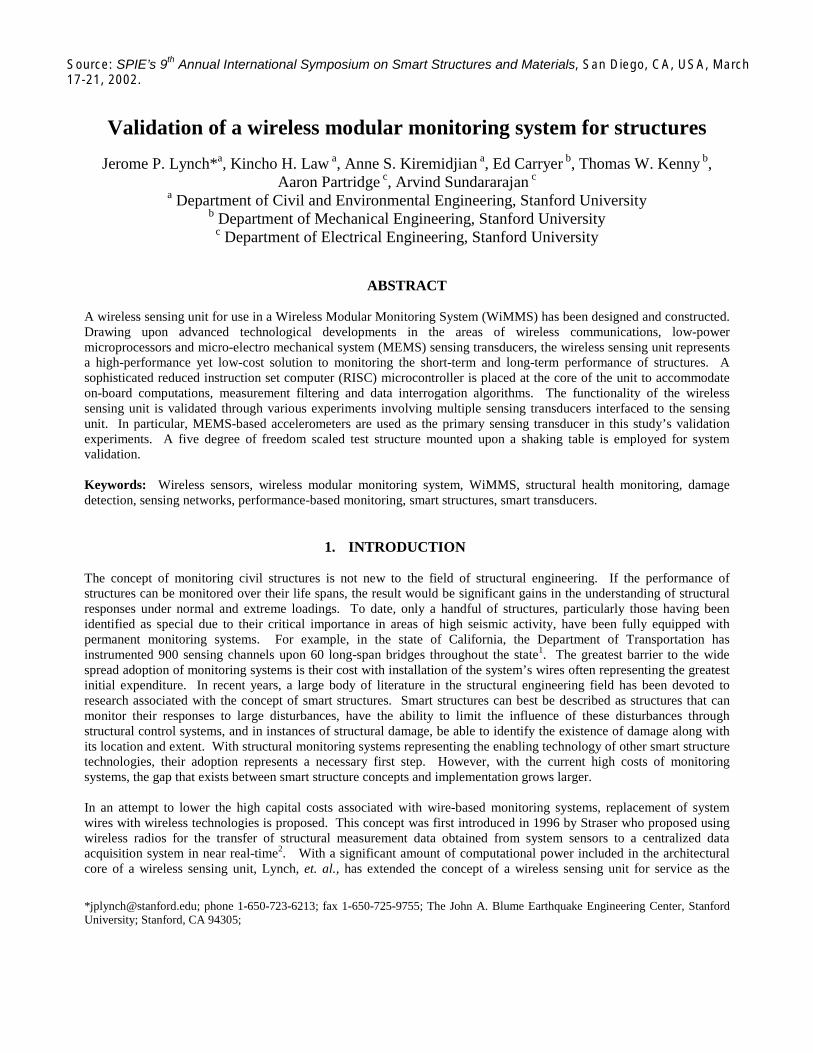
The complete hardware design of the wireless sensing unit can be partitioned into three segments: the sensing interface,the computational core, and wireless communications (Fig. 1). The sensing interface is responsible for the interface ofsensors to the wireless sensing unit and the conversion of their measurements to a digital format. The resulting digitalmeasurements are then sent to the computational core where the overall operation of the wireless sensing unit isconducted. After the data has been logged and interrogated at the core, the data is packaged for transmission upon thewireless communication channel. In the following sections, each of these three functional groups of the proposedwireless sensing unit is discussed in greater detail.
2.1 Sensing interfaceA large number of sensors can be employed for the purpose of monitoring structures. Accelerometers are a traditionalchoice for monitoring the global response of structures while strain gages and crack sensors are typically used for localresponse monitoring. To ensure a versatile and effective wireless sensing unit, the unit is designed to be sensortransparent by allowing the sensing interface to accept sensors that have analog outputs ranging in voltage from 0 to 5volts. Transduction specifications unique to each sensor, such as conversion constants, can be coded into thecomputational core for the calculation of physical measurements from their analog voltage signals. A single channel,low-noise, Texas Instrument 16-bit analog-to-digital (A/D) converter is used for resolving to digital form, the analogoutput of a sensor. The high speed parallel CMOS architecture of the A/D allows for data sampling rates as high as 1000kHz. Classical global response monitoring systems do not require sampling rates this high, but novel damage detectionprocedures based on local response data could require sampling rates in the kHz region.
In addition to the A/D converter, a dual axes MEMS-based accelerometer is permanently interfaced to the core’smicrocontroller. The Analog Devices’ ADXL210 accelerometer was selected to interface directly to the system becauseit has the ability to output acceleration readings in a digital format that is easily readable by the computational core.Therefore, the acceleration output of the accelerometer’s two orthogonal sensing axes serve as additional sensingchannels included in the unit design, bringing the total number of data acquisition channels to three.
2.2 Computational coreThe computational core of the wireless sensing unit represents the single most important design decision since itscapabilities have a direct influence upon the performance and limitations of the entire unit. Three design factors governthe selection process of the computational core: computational capabilities, power consumption, and cost. Amicrocontroller which maximizes computation capabilities per unit power and cost is sought.
The final selection is an 8-bit microcontroller from the Atmel AVR family. This high-performance and low-powermicrocontroller is of a reduced instruction set computer (RISC) architecture providing 118 powerful assemblyinstructions that are executed on a single clock cycle. A maximum 8 million instructions per second (MIPS) throughputcan be attained with this microcontroller. A suite of peripheral features provided on-chip includes timers, counters,analog comparators, and a programmable serial UART6. Sufficient memory is provided for storing the operational codeof the computational core: 8K bytes of programmable flash memory, 512 bytes of static random access memory(SRAM) and 512 bytes of electronically erasable programmable read-only memory (EEPROM).
A convenient feature of the Atmel microcontroller is that its architectural design is optimized for use with high-levellanguages such as C and C++ when programming the microcontroller7. In general, high level languages employed forprogramming adds significant overhead in the microcontroller’s code execution since the microcontrollers are optimizedwith the assumption that they would be programmed using assembly instructions. By providing 32 8-bit general purposeregisters with 3 16-bit pointers, the Atmel AVR microcontroller reduces code overhead and allows for high code densitywhen using high-level languages for programming. The large number of general purpose registers is necessary forallowing local variable definitions while the 3 16-bit pointers are useful for allowing indirect jumps and elegant datamemory accessing.
2.3 Wireless communicationsA reliable means of communicating measurement data from the wireless sensing unit to the network of wireless sensorsis sought. While many wireless technologies exist in the marketplace, only those modems that employ spread spectrumtechniques are considered. By avoiding the concentration of information on a single frequency, spread spectrum radiosencode data over a wide frequency band. The low power, noise-like signals emitted from a spread spectrum transmitterare hard to intercept and jam making them robust and highly-reliable.
The Proxim RangeLAN2 radio modem is selected to serve as the wireless technology for the sensing unit. Operating onthe 2.4 GHz unregulated FCC band, the RangeLAN2 communicates at a data rate of 1.6 Mbps. By employing a 1dBi
WirelessCommunications
Computational CoreSensing Interface
16-bitAnalog-Digital
Converter(Single Channel)
RISC MicrocontrollerAtmel AVR
AnalogSensor
0-5V0110101
Dual Axis (X,Y)MEMS Accelerometer
ADXL210
X-Axis
Y-Axis
Proxim RangeLan2Wireless Modem
Serial Port Serial Port
8K Bytes Flash ROM
512 Bytes SRAM
512 Bytes EEPROM
Data Memory Buffer
Spread SpectrumEncoding
Fig. 1: Functional layout of proposed wireless sensing unit

omni-directional antenna, open space communication ranges of 1000 feet can be attained while inside structures, thisrange would be reduced to approximately 500 feet with the range varying as a function of the type of buildingconstruction8. Powered by a 9 V direct current (DC) voltage source, the modem draws 160mA of current during receiveand transmit communications, but its current draw can be reduced to 60mA when the modem is placed in sleep mode.Sleep mode is important if a battery is employed since this convenient feature can extend the life of the battery.
2.4 Integration and packagingWith the key hardware components selected, the system is integrated in one package. The integrated circuit componentssuch as the microcontroller, A/D converter and additional support circuitry are mounted upon a two layer circuit boarddesigned using a noise minimization approach. The RangeLAN2 radio gear is externally attached to the circuit boardthrough an RS232 serial cable. The entire packaging is powered by a 9 V alkaline battery power supply. Thedimensions of the system are 4 inches long, 4 inches wide, and 2 inches deep (Fig 2).
3. WIRELESS SENSING UNIT PERFORMANCE VALIDATION
With the design of the wireless sensing unit complete and a prototype fully constructed, it is necessary to perform aseries of validation tests to ensure suitable performance for structural monitoring applications. The first set of validationtests intend to evaluate the performance of the individual wireless sensing unit. The duration of the unit’s power source,the resolution of the A/D converter, and the maximum permissible sample rate for data acquisition are to determined.
3.1 Battery life spanThe sensing unit requires a 9 volt DC power source. One potential source of power can originate from a portable powersource such as a 9 volt battery. However, the amount of power contained in a battery source is finite and will eventuallyrun out if not recharged or replaced. Based on the electrical characteristics of the various sensing unit components, theexpected operating life of the system’s power source can easily be calculated. For example, the Proxim RangeLAN2draws 160mA when transmitting data and 60 mA when placed in sleep mode. The data sheet of a Duracell 9 V alkaline-manganese dioxide battery provides a log-log engineering design chart of the battery’s service life versus dischargecurrent9. Considering the driving current of the RangeLAN modem and consulting the engineering chart of the battery,the life span of the 9 V battery when the modem is transmitting data is roughly 2 hours while in sleep mode, the batterycan last roughly 4 hours. Considering the electrical characteristics of the various integrated circuits chosen such as themicrocontroller and A/D converter, the approximate current draw of the unit’s circuit is 27 mA. When a 9 V Duracellbattery is selected to power the circuit, the expected operational life span of the battery is as high as 20 hours.
Fig. 2: Fully functional wireless sensing unit prototype

To validate these calculations of the expected operational life of the sensing unit, the sensing unit is operated using aDuracell 9 V battery with the operational life of the battery monitored (Fig. 3). The results of the battery test are in goodagreement with the initial life span estimates. The short life span of the 9V battery, especially during the operation ofthe radio modem, underscores the fact that power is an important design issue of the prototype and should be revisited inthe future. While outside the scope of this study, more efficient batteries do exist in the marketplace that can be used inlieu of the 9 V alkaline batteries to provide a significantly longer lasting 9 V DC power source. Renewable nickelcadmium battery sources, coupled with a mechanism of recharging, can also be considered in future sensing unitdesigns.
3.2 A/D ResolutionThe A/D converter is located on the unit’s two-layer circuit board, sharing power and grounding lines with the otherintegrated circuit components including analog and digital logic components. When digital and analog integratedcircuits share a common ground, ordinary switching of the digital logic can have a detrimental influence on theperformance of the analog circuit10. The analog portion of the A/D converter, with a starting conversion resolution of 16bits, is susceptible to some amount of corruption of the analog signal input due to the digital switching elsewhere in thecircuit. The result is seen as a reduction in the digital resolution of the A/D converter. To test for this reduction, a high-performance regulated power supply is used to hold a constant voltage at the sensor input of the A/D converter. Thepower supply used is a Hewlett Package E3610A with an output ripple and noise of only 200 µV. Assuming the fullresolution of 16 bits in the conversion, the noise in the regulated power supply output would result in the chattering ofthe two least significant bits of the digital conversion. The output of the A/D converter has noise greater than that of thepower supply, representing a manifestation of the A/D converter’s reduced resolution (Fig. 4). The conversion noise isrelatively white, with a standard deviation of +5 bit counts, representing a resolution of approximately 13 bits.
3.3 Data acquisition sample rateThe wireless sensing unit can be used for both real-time and near real-time monitoring applications. For near real-timeapplications, the sensing unit is programmed to locally accumulate data at a given rate and to store that data for laterretrieval. When the data collection is complete and the sensor data stored in memory, the unit can transmit that data tothe other wireless sensing units in the sensing network upon demand. The delay in archiving and transmitting the sensor
Fig. 4: Performance of the A/D converter – Constant voltage of 1.5V applied
0 2 4 6 8 10 12 14 16 181.976
1.977
1.978
1.979
1.98
1.981x 10
4
Time (seconds)
Dig
italO
utpu
tof
A/D
-10 -5 0 5 100
0.1
0.2
0.3
Per
cent
Sam
ples
Offset Digital Count
Fig. 3: Operational life span of the wireless sensing unit’s components when powered by a 9V battery
Modem Tx
Modem Sleep
Unit Circuit Board
2.25 Hours
3.8 Hours
21 Hours

data results in this approach being classified as near real-time. In contrast, for real-time applications, the microcontrolleris responsible for transmitting data at a precise clock time. In real-time data acquisition applications, the data is stillarchived locally in memory.
Prior to implementation, the sample rate of the wireless sensing unit can be set to a desired value depending upon themonitoring application. In both modes of operation, there exist maximum sampling rates that the sensing unit canachieve. For real-time applications, time is required to encode each data point within a packet protocol specific to theRangeLAN2 radio modem. Once assembled in the microcontroller, more time is required to send the packet through theserial port to the radio. A baud rate of 19200 is used where the baud rate represents a direct measure of the maximumnumber of times a digital signal can vary per second on a single electrical line. Once the packet is buffered in theRangeLAN2 packet buffer, additional time is required to employ spread spectrum techniques for the transmission of thepacket. Validation tests are performed, indicating that this entire process results in a maximum real-time sampling rateof 33 Hz. If a sampling rate is chosen greater than the 33 Hz threshold, data points can be lost during transmission. Fornear real-time applications, only the time required to attain and save the data in memory limits the maximum samplingrate. Empirical tests indicate that for near real-time, a maximum sampling rate of 20 kHz can be attained.
4. MEMS-BASED ACCELEROMETERS
Complementing the low-cost nature of the proposed wireless sensing unit, the feasibility of interfacing inexpensive andcompact sensors to the unit is of particular interest. The field of micro-technologies is fabricating small micrometersized mechanical transducers upon the same silicon die used for integrated circuits, yielding low cost and precise MEMSsensors in form factors unimaginable years ago. Given the wide spread popularity of using accelerometers to monitorthe global response of structural systems to dynamic loads, MEMS-based accelerometers are selected from availableMEMS sensors. Two distinctly different MEMS accelerometer architectures are considered in this study: capacitive andpiezoresistive designs. The Analog Devices ADXL210 and Bosch SMB110 accelerometers are selected from the familyof capacitive designs while a new piezoresistive accelerometer is designed and fabricated for this study.
4.1 Capacitive architecturesEmploying advanced photolithography and etching techniques during manufacturing, a three dimensional polysiliconstructure consisting of a released proof mass can be fabricated11. The proof mass is connected to the silicon substratethrough linear springs. Capacitive plates are etched into the perimeters of both the proof mass and substrate formingbalanced differential capacitors that are used to directly measure acceleration (Fig. 5). The substrate’s capacitor platesare driven 180° out of phase with voltage square waves. As the capacitive plate of the proof mass displaces between thetwo plates of the substrate, it unbalances the differential capacitor resulting in a square wave signal whose amplitude isproportional to the displacement. A synchronous demodulator is then used to generate an analog signal from thedifferential capacitor proportional to the acceleration of the sensor. The characteristics of the accelerometer’sperformance such as bandwidth and resolution can be set by connecting a capacitor on the analog output completing afirst-order RC low pass filter. In general, a tradeoff exists between the bandwidth and resolution of the accelerometerwith greater bandwidths causing reduced resolution. The noise inherent in capacitive accelerometers is characteristicallyGaussian and is therefore constant over the entire bandwidth of the sensor.
In the capacitive accelerometer family, two accelerometers are considered for integration with the sensing unit. TheBosch SMB110 and Analog Devices ADXL210 are selected. Variations exist in the design of the two accelerometers.In particular, the SMB110 is a single axis accelerometer while the ADXL210 measures acceleration in two planar axes.It was already noted that an ADXL210 sensor is directly interfaced to the microcontroller, but for this study’s validationtests, an additional ADXL210 is externally connected through the A/D converter. When interfaced directly to themicrocontroller, the advantage of using the optional digital output of the ADXL210 accelerometer is exploited. TheADXL210 encodes its acceleration measurements within the duration of the high portion of a continuous square wave.This digital technique is called duty cycle modulation. The resolution of this duty cycle modulated signal is 14-bit andanti-aliased. The performance properties of the two capacitive accelerometers are summarized in Table 1.
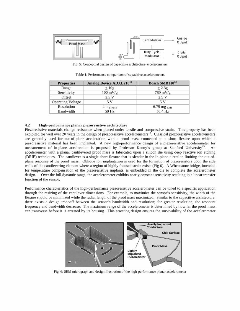
Table 1: Performance comparison of capacitive accelerometers
Properties Analog Device ADXL21012 Bosch SMB11013
Range + 10g + 2.3gSensitivity 100 mV/g 780 mV/g
Offset 2.5 V 2.5 VOperating Voltage 5 V 5 V
Resolution 4 mg RMS 6.79 mg RMS
Bandwidth 50 Hz 56.4 Hz
4.2 High-performance planar piezoresistive architecturePiezoresistive materials change resistance when placed under tensile and compressive strain. This property has beenexploited for well over 20 years in the design of piezoresistive accelerometers14. Classical piezoresistive accelerometersare generally used for out-of-plane acceleration with a proof mass connected to a short flexure upon which apiezoresistive material has been implanted. A new high-performance design of a piezoresistive accelerometer formeasurement of in-plane acceleration is proposed by Professor Kenny’s group at Stanford University15. Anaccelerometer with a planar cantilevered proof mass is fabricated upon a silicon die using deep reactive ion etching(DRIE) techniques. The cantilever is a single short flexure that is slender in the in-plane direction limiting the out-of-plane response of the proof mass. Oblique ion implantation is used for the formation of piezoresistors upon the sidewalls of the cantilevering element where a region of highly focused strain exists (Fig 6). A Wheatstone bridge, intendedfor temperature compensation of the piezoresistive implants, is embedded in the die to complete the accelerometerdesign. Over the full dynamic range, the accelerometer exhibits nearly constant sensitivity resulting in a linear transferfunction of the sensor.
Performance characteristics of the high-performance piezoresistive accelerometer can be tuned to a specific applicationthrough the resizing of the cantilever dimensions. For example, to maximize the sensor’s sensitivity, the width of theflexure should be minimized while the radial length of the proof mass maximized. Similar to the capacitive architecture,there exists a design tradeoff between the sensor’s bandwidth and resolution; for greater resolution, the resonantfrequency and bandwidth decrease. The maximum range of the accelerometer is determined by how far the proof masscan transverse before it is arrested by its housing. This arresting design ensures the survivability of the accelerometer
Proof MassDemodulator
Duty CycleModulator
AnalogOutput
DigitalOutput
Fig. 5: Conceptual design of capacitive architecture accelerometers
LightlyImplantedPiezoresistor
Proof Mass
Chip Surface
Heavily ImplantedConductors
Fig. 6: SEM micrograph and design illustration of the high-performance planar accelerometer
when mechanically shocked. This is a major advantage of the accelerometer since the capacitive designs sustain damagewhen shocked. The end stops of the proof mass also prevent the flexural element from entering a nonlinear responseregime.
Two dominant noise sources are present in the accelerometer design. In lower frequency regions, roughly below 100Hz, noise is attributed to the inverse frequency (1/f) Hooge electrical noise of the piezoresistive elements16. Aboveapproximately 100 Hz, Johnson noise is the dominate noise source and is constant over the applicable frequency region.Johnson noise is a direct result of the thermal agitation of electrons in a conductive element.
When compared against commercially available piezoresistive accelerometers, the experimental results of the high-performance piezoresistive accelerometer is superior. One set of accelerometers are designed and fabricated for specificadoption within the wireless structural sensing unit. These particular accelerometers have a radial length of 1 mm and aflexural width of 5 µm. The full dynamic range of the accelerometers is well above 10g with a resolution of 20 µg at anacceleration bandwidth of 650 Hz.
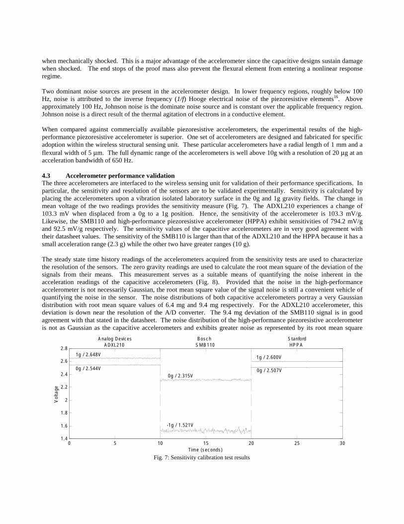
4.3 Accelerometer performance validationThe three accelerometers are interfaced to the wireless sensing unit for validation of their performance specifications. Inparticular, the sensitivity and resolution of the sensors are to be validated experimentally. Sensitivity is calculated byplacing the accelerometers upon a vibration isolated laboratory surface in the 0g and 1g gravity fields. The change inmean voltage of the two readings provides the sensitivity measure (Fig. 7). The ADXL210 experiences a change of103.3 mV when displaced from a 0g to a 1g position. Hence, the sensitivity of the accelerometer is 103.3 mV/g.Likewise, the SMB110 and high-performance piezoresistive accelerometer (HPPA) exhibit sensitivities of 794.2 mV/gand 92.5 mV/g respectively. The sensitivity values of the capacitive accelerometers are in very good agreement withtheir datasheet values. The sensitivity of the SMB110 is larger than that of the ADXL210 and the HPPA because it has asmall acceleration range (2.3 g) while the other two have greater ranges (10 g).
The steady state time history readings of the accelerometers acquired from the sensitivity tests are used to characterizethe resolution of the sensors. The zero gravity readings are used to calculate the root mean square of the deviation of thesignals from their means. This measurement serves as a suitable means of quantifying the noise inherent in theacceleration readings of the capacitive accelerometers (Fig. 8). Provided that the noise in the high-performanceaccelerometer is not necessarily Gaussian, the root mean square value of the signal noise is still a convenient vehicle ofquantifying the noise in the sensor. The noise distributions of both capacitive accelerometers portray a very Gaussiandistribution with root mean square values of 6.4 mg and 9.4 mg respectively. For the ADXL210 accelerometer, thisdeviation is down near the resolution of the A/D converter. The 9.4 mg deviation of the SMB110 signal is in goodagreement with that stated in the datasheet. The noise distribution of the high-performance piezoresistive accelerometeris not as Gaussian as the capacitive accelerometers and exhibits greater noise as represented by its root mean square
Fig. 7: Sensitivity calibration test results
0 5 10 15 20 25 301.4
1.6
1.8
2
2.2
2.4
2.6
2.8
Time (seconds)
Vol
tage
Analog DevicesADXL210
BoschSMB110
StanfordHPPA
0g / 2.507V
1g / 2.648V
-1g / 1.521V
1g / 2.600V
0g / 2.315V
0g / 2.544V
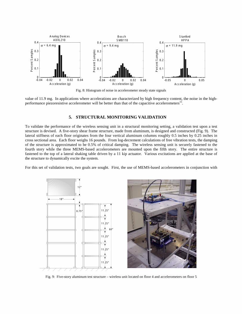
value of 11.9 mg. In applications where accelerations are characterized by high frequency content, the noise in the high-performance piezoresistive accelerometer will be better than that of the capacitive accelerometers15.
5. STRUCTURAL MONITORING VALIDATION
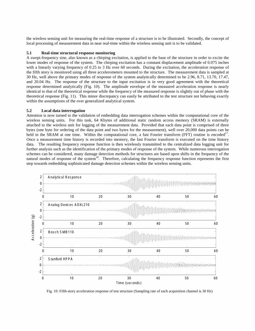
To validate the performance of the wireless sensing unit in a structural monitoring setting, a validation test upon a teststructure is devised. A five-story shear frame structure, made from aluminum, is designed and constructed (Fig. 9). Thelateral stiffness of each floor originates from the four vertical aluminum columns roughly 0.5 inches by 0.25 inches incross sectional area. Each floor weighs 16 pounds. From log-decrement calculations of free vibration tests, the dampingof the structure is approximated to be 0.5% of critical damping. The wireless sensing unit is securely fastened to thefourth story while the three MEMS-based accelerometers are mounted upon the fifth story. The entire structure isfastened to the top of a lateral shaking table driven by a 11 kip actuator. Various excitations are applied at the base ofthe structure to dynamically excite the system.
For this set of validation tests, two goals are sought. First, the use of MEMS-based accelerometers in conjunction with
Fig. 8: Histogram of noise in accelerometer steady state signals
-0.04 -0.02 0 0.02 0.040
0.1
0.2
0.3
0.4
Per
cent
Sam
ples
Acceleration (g)
σ = 6.4 mg
-0.04 -0.02 0 0.02 0.040
0.1
0.2
0.3
0.4
Per
cent
Sam
ples
Acceleration (g)-0.05 0 0.05
0
0.1
0.2
0.3
0.4
Per
cent
Sam
ples
Acceleration (g)
Analog DevicesADXL210
BoschSMB110
StanfordHPPA
σ = 9.4 mg σ = 11.9 mg
18"
12"
0.75" 11.25"
11.25"
11.25"
11.25"
11.25"
60"
Fig. 9: Five-story aluminum test structure – wireless unit located on floor 4 and accelerometers on floor 5
the wireless sensing unit for measuring the real-time response of a structure is to be illustrated. Secondly, the concept oflocal processing of measurement data in near real-time within the wireless sensing unit is to be validated.
5.1 Real-time structural response monitoringA swept-frequency sine, also known as a chirping excitation, is applied to the base of the structure in order to excite thelower modes of response of the system. The chirping excitation has a constant displacement amplitude of 0.075 incheswith a linearly varying frequency of 0.25 to 3 Hz over 60 seconds. During the excitation, the acceleration response ofthe fifth story is monitored using all three accelerometers mounted to the structure. The measurement data is sampled at30 Hz, well above the primary modes of response of the system analytically determined to be 2.96, 8.71, 13.70, 17.47,and 20.04 Hz. The response of the structure to the input excitation is in very good agreement with the theoreticalresponse determined analytically (Fig. 10). The amplitude envelope of the measured acceleration response is nearlyidentical to that of the theoretical response while the frequency of the measured response is slightly out of phase with thetheoretical response (Fig. 11). This minor discrepancy can easily be attributed to the test structure not behaving exactlywithin the assumptions of the over generalized analytical system.
5.2 Local data interrogationAttention is now turned to the validation of embedding data interrogation schemes within the computational core of thewireless sensing units. For this task, 64 Kbytes of additional static random access memory (SRAM) is externallyattached to the wireless unit for logging of the measurement data. Provided that each data point is comprised of threebytes (one byte for ordering of the data point and two bytes for the measurement), well over 20,000 data points can beheld in the SRAM at one time. Within the computational core, a fast Fourier transform (FFT) routine is encoded17.Once a measurement time history is recorded into memory, the fast Fourier transform is executed on the time historydata. The resulting frequency response function is then wirelessly transmitted to the centralized data logging unit forfurther analysis such as the identification of the primary modes of response of the system. While numerous interrogationschemes can be considered, many damage detection methods for structures are based upon shifts in the frequency of thenatural modes of response of the system18. Therefore, calculating the frequency response function represents the firststep towards embedding sophisticated damage detection schemes within the wireless sensing units.
Fig. 10: Fifth-story acceleration response of test structure (Sampling rate of each acquisition channel is 30 Hz)
0 10 20 30 40 50 60
-2
0
2
Acc
eler
atio
n(g
)
0 10 20 30 40 50 60
-2
0
2
0 10 20 30 40 50 60
-2
0
2
0 10 20 30 40 50 60
-2
0
2
Time (seconds)
Analytical Response
Analog Devices ADXL210
Bosch SMB110
Stanford HPPA
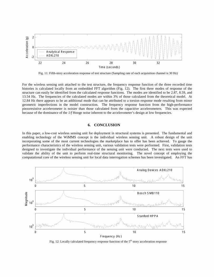
For the wireless sensing unit attached to the test structure, the frequency response function of the three recorded timehistories is calculated locally from an embedded FFT algorithm (Fig. 12). The first three modes of response of thestructure can easily be identified from the calculated response functions. The modes are identified to be 2.87, 8.59, and13.54 Hz. The frequencies of the calculated modes are within 3% of those calculated from the theoretical model. At12.84 Hz there appears to be an additional mode that can be attributed to a torsion response mode resulting from minorgeometric imperfections in the model construction. The frequency response function from the high-performancepiezoresistive accelerometer is noisier than those calculated from the capacitive accelerometers. This was expectedbecause of the dominance of the 1/f Hooge noise inherent to the accelerometer’s design at low frequencies.
6. CONCLUSION
In this paper, a low-cost wireless sensing unit for deployment in structural systems is presented. The fundamental andenabling technology of the WiMMS concept is the individual wireless sensing unit. A robust design of the unitincorporating some of the most current technologies the marketplace has to offer has been achieved. To gauge theperformance characteristics of the wireless sensing unit, various validation tests were performed. First, validation testsdesigned to investigate the individual performance of the sensing unit were conducted. The next tests were used tovalidate the ability of the unit to perform real-time structural monitoring. The novel concept of employing thecomputational core of the wireless sensing unit for local data interrogation schemes has been investigated. An FFT has
Fig. 11: Fifth-story acceleration response of test structure (Sampling rate of each acquisition channel is 30 Hz)
22 24 26 28 30 32
-2
0
2
Acc
eler
atio
n(g
)
Time (seconds)
Analytical ResponseADXL210
Fig. 12: Locally calculated frequency response function of the 5th story acceleration response
0 5 10 15
100
0 5 10 15
100
Mag
nitu
de
0 5 10 15
100
Frequency (Hz)
Analog Devices ADXL210
Bosch SMB110
Stanford HPPA

been successfully implemented and the primary modes of response of a structure identified locally by a wireless sensingunit mounted upon a test structure.
Future work is still needed to improve the hardware capabilities of the wireless sensing unit. Particularly, powerconsumption of the wireless radios is a concern and will be addressed in next generation designs. Furthermore, a morepowerful computational core is sought. More power in the core directly translates into more sophisticated datainterrogation schemes that can be performed in near real-time with the ultimate goal of incorporating data detectionschemes that can hypothesis damage occurrence, location and severity.
ACKNOWLEDGEMENTS
The authors would like to express their gratitude to Dr. S.C. Liu of the National Science Foundation for encouragementand support of research in low-cost wireless sensing systems for structures. The fruitful suggestions provided by Dr.Chuck Farrar and Dr. Hoon Sohn of Los Alamos National Labs, have been invaluable to the progress of our research.We gratefully acknowledge the samples of MEMS-based accelerometers (SMB110) provided by Robert Bosch GmbH.This research is partially funded by the National Science Foundation under grant number CMS-9988909.
REFERENCES
1. P. Hipley, “Caltrans’ current state-of-practice,” Proceedings of COSMOS Instrumental Systems for Diagnostics of SeismicResponse of Bridges and Dams, pp. 3-7, 2001.
2. E. G. Straser, A. S. Kiremidjian, T. H. Meng, and L. Redlefsen, “Modular, wireless network platform for monitoring structures,”Proceedings of the International Modal Analysis Conference – IMAC, pp. 450-456, 1998.
3. J. P. Lynch, K. H. Law, A. S. Kiremidjian, T. W. Kenny, and E. Carryer, “A wireless modular monitoring system for civilstructures,” Proceedings of the International Modal Analysis Conference – IMAC, 2002.
4. P. B. Chu, N. R. Lo, E. C. Berg, and K. S. Pister, “Optical communication using micro corner cube reflectors,” Proceedings ofthe 10th IEEE International Workshop on Micro-Electro-Mechanical Systems, pp. 350-355, 1997.
5. M. R. Moore, S. F. Smith, and K. Lee, “Next-step a wireless IEEE 1451 standard for smart sensor networks,” Sensors Magazine18(9), pp. 26-33, 2001.
6. AVR RISC Microcontroller Data Book, Atmel Corporation, August 1999.7. A. E. Bogen and V. Wollan, “AVR Enhanced RISC Microcontrollers,” Atmel Technical Document, Atmel Corporation, 1999.8. Proxim RangeLAN2 Serial Adapter Model 7910 and 7911 User’s Guide, Proxim Corporation, 1999.9. Alkaline-Manganese Dioxide Battery 9V (6LR61) Data Sheet, Duracell Corporation, May 2000.10. P. Horowitz and W. Hill, The Art of Electronics, p. 565-672, Cambridge University Press, Cambridge, 1989.11. H. Weinberg, “Dual axis, low g, fully integrated accelerometers,” Analog Dialogues 33(1), pp. 1-2, 1999.12. Low-cost + 2g/ +10g Dual Axis iMEMS Accelerometers with Digital Output ADXL202/ADXL210 Data Sheet, Analog Devices
Corporation, 1999.13. SMB110 Technical Customer Documentation: Low-g Accelerometer for Safety and Comfort Applications, Robert Bosch GmbH,
October 1999.14. L. M. Roylance and J. B. Angell, “A batch fabricated silicon accelerometer,” IEEE Transactions on Electron Devices 26, pp.
1911-1917, December 1979.15. A. Partridge, J. K. Reynolds, B. W. Chui, E. M. Chow, A. M. Fitzgerald, L. Zhang, N. I. Maluf, and T. W. Kenny, “A high-
performance planar piezoresistive accelerometer,” Journal of Microelectromechanical Systems 9(1), March 2000.16. F. N. Hooge, “1/f noise sources,” IEEE Transactions of Electron Devices 41, pp. 1926-1935, November 1994.17. W. H. Press, S. A. Teukolsky, W. T. Vetterling, and B. P. Flannery, Numerical Recipes in C, p. 496-536, Cambridge University
Press, Cambridge, 1992.18. S. W. Doebling, C. R. Farrar, M. B. Prime, and D. W. Shevitz, “Damage identification and health monitoring of structural and
mechanical systems from changes in their vibration characteristics: a literature review,” Los Alamos National Laboratory ReportLA-13070-MS, May 1996.
1 COSMOS2 Straser thesis3 My paper – IMAC 3rd International Workshop at Stanford4 Pister paper5 Sensor article6 Atmel Data Book7 Atmel Document8 Proxim RangeLAN2 documentation9 Duracell Design Document10 Noise in electrical circuit boards (Horowitz and Hill?)11 AD Dialogues12 ADXL210 Data Sheet13 Bosch Datasheet14 Roylance and Angell15 Partridge paper16 Hooge17 Numerical Recipes18 Damage detection reference


