Valente - SRF thin films produced by energetic condensation
59
Anne-Marie VALENTE-FELICIANO J. Spradlin, L. Phillips, C. Reece, B. Xiao, X. Zhao R.A. Lukazew, D. Beringer D. Gu K. Seo 4th International Workshop on thin Films and New Ideas for Pushing the Limits of RF Superconductivity
-
Upload
thinfilmsworkshop -
Category
Technology
-
view
673 -
download
1
Transcript of Valente - SRF thin films produced by energetic condensation

Anne-Marie VALENTE-FELICIANO
J. Spradlin, L. Phillips, C. Reece, B. Xiao, X. Zhao
R.A. Lukazew, D. Beringer
D. Gu
K. Seo
4th International Workshop on thin Films and New Ideas for Pushing the Limits of RF Superconductivity
OUTLINE
Approach
Nb growth on Sapphire
Nb growth on MgO
Nb growth on Cu surfaces
Concluding Remarks
4th International Workshop on thin Films and New Ideas for Pushing the Limits of RF Superconductivity - A-M Valente-Feliciano

Approach
4th International Workshop on thin Films and New Ideas for Pushing the Limits of RF Superconductivity - A-M Valente-Feliciano
Engineered Nb films:
Growing and characterizing niobium films with controlled deposition energy and substrate temperature via Electron Cyclotron Resonance (ECR) and High Power Impulse Magnetron Sputtering (HIPIMS) in self-sputtering mode.Monitoring in-situ crystal character dependence on substrate properties and deposition parameters.
Film growth approach in 3 sequential phases:
Film nucleation on the substrate (Nb, Al2O3, Cu; single crystal & polycrystalline)Growth of an appropriate template for subsequent deposition of the final
RF surfaceDeposition of the final surface optimized for minimum defect density.
Engineered Nb films & SIS Multilayer Structures
In the framework of a collaboration with surrounding universities, JLAb is exploring 2 opportunities:

Tailoring for optimum RF performance
Careful characterization of the attained composition and
microstructure
Close association with resulting rf surface impedance and
superconducting properties
4th International Workshop on thin Films and New Ideas for Pushing the Limits of RF Superconductivity - A-M Valente-Feliciano

Connecting Structure & Performance for SRF Surfaces
involves understanding
of
The chemistry of the involved speciesReactivityStoichiometric sensitivityReaction process temperatures
Crystal structure dependence on substrate structureInfluence of deposition energy on resulting structureSensitivity to the presence of contaminating speciesStabilization of desired film against subsequent degradation
Characterization of deposited film surfaces In-situ crystallographic structure characterization – (RHEED), Scanning Tunneling Microscopy (STM)Large area crystallographic structure – X-ray diffraction (XRD)10 nm-scale crystallographic texture within ~ 50 nm of surface – Electron backscatter diffraction (EBSD) Topography – stylus profilometry, atomic force microscopy (AFM), optical profilometryNear surface (< 8 nm) chemistry – X-ray photoelectron spectroscopy (XPS)Micro-contaminant defects – Secondary ion mass spectrometry, with standards (SIMS)Structural cross-section of film – Transmission electron microscopy (TEM), Focused Ion Beam (FIB).
4th International Workshop on thin Films and New Ideas for Pushing the Limits of RF Superconductivity - A-M Valente-Feliciano

Connecting Structure & Performance for SRF Surfaces
• surface self-diffusion• competitive grain growth• defect density• back-sputtering• preferential sputtering rates
Grain boundaries have an effect on surface resistance.
Film quality is dependent on deposition technique:
• surface roughness• defect density• Back-sputtering from energetic condensation
4th International Workshop on thin Films and New Ideas for Pushing the Limits of RF Superconductivity - A-M Valente-Feliciano

Measurement with the SIC cavity (TE011 sapphire-loaded cylindrical Nb cavity) Surface impedance as a function of magnetic field and temperature from 1.9 K to 4.8 K.Normal state surface impedance at 10 K, from which the surface value of electronic mean free path and surface Hc1 can be determined.Superconducting penetration depth, λ, at low field will be measured by carefully tracking the cavity frequency with temperature as the sample temperature is swept slowly back and forth across the transition temperature (SIC sensitivity: 30 Hz/nm) while the rest of the cavity is held at 2 K.
Tc – easy coarse measure of intra-grain quality of the film RRR – convenient assessment of aggregate defect density
Connecting Structure & Performance for SRF Surfaces
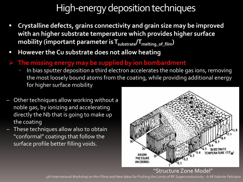
High-energy deposition techniques
Crystalline defects, grains connectivity and grain size may be improved with an higher substrate temperature which provides higher surface mobility (important parameter is Tsubstrate/Tmelting_of_film)
However the Cu substrate does not allow heating
The missing energy may be supplied by ion bombardment In bias sputter deposition a third electron accelerates the noble gas ions, removing
the most loosely bound atoms from the coating, while providing additional energy for higher surface mobility
“Structure Zone Model”
– Other techniques allow working without a noble gas, by ionizing and accelerating directly the Nb that is going to make up the coating
– These techniques allow also to obtain “conformal” coatings that follow the surface profile better filling voids.
4th International Workshop on thin Films and New Ideas for Pushing the Limits of RF Superconductivity - A-M Valente-Feliciano

Film growth
4th International Workshop on thin Films and New Ideas for Pushing the Limits of RF Superconductivity - A-M Valente-Feliciano
The grain size of a polycrystalline film is affected by:• The substrate temperature during deposition (high for large grains)• Adatom diffusivity (high)• The annealing temperatures (high)• The deposition flux (low)• The impurity content (low)• The film thickness (high)* Energy of the deposited atom (high)• Energy of bombarding ions/atoms (high)* Tm of Material (low)• The materials class (metals)

Energetic Condensation via ECRNiobium vapour produced by an e-beam gun is ionized by an ECR process. The Nb ions can be accelerated to the substrate by an appropriate bias. Energies in excess of 100 eVcan be obtained.
Generation of plasma
3 essential components:Neutral Nb vaporRF power (@ 2.45GHz)Static B ERF with ECR condition
Why ECR?No working gas
High vacuum ie. reduced impurities
Singly or “quasi-singly charged” ions
Controllable deposition energy
90 deposition flux
(Possible to help control the crystal structure)
Excellent bonding
No macro particles
Faster rate (Conditional)
Wu, G., et al. J. Vac. Sci. Technol. A Vol. 21, No. 4, (2003)
m
eB
4th International Workshop on thin Films and New Ideas for Pushing the Limits of RF Superconductivity - A-M Valente-Feliciano

Energetic vacuum deposition by ECR plasma
4th International Workshop on thin Films and New Ideas for Pushing the Limits of RF Superconductivity - A-M Valente-Feliciano

Nucleation studies in UHV deposition system at the College William & Mary
In-situ observation of the nucleation and subsequent growth with coating parameters, annealing… on single crystal and polycrystalline substrates.
UHV system with in-situ RHEED & STM
4th International Workshop on thin Films and New Ideas for Pushing the Limits of RF Superconductivity - A-M Valente-Feliciano

Samples produced on different substratesInsulating:
Al2O3 (11-20)Al2O3 (11-20)MgO(100)SrTiO3
Metallic:Cu (100)Cu (110)Cu (111)
Fine grain CuLarge grain Cu
Typical vacuum during plasma in ECR system:<5x10⁻⁸ Torr4th International Workshop on thin Films and New Ideas for Pushing the Limits of RF Superconductivity - A-M Valente-Feliciano

ECR growth rate
Films with thicknesses up to 4mm with 0V bias and 2mm with 120V bias have been produced
No problem of de-lamination for thick films even when important lattice mismatch as on Cu and MgO
Only peel-off issue on Cu when heated to temperatures higher than 400°C due to roughening (P. Zeppenfeld et al., PRL 62,1, Jan 89)
Troughening Cu (111)~400°CTroughening Cu (110), (100)>700°C
Adhesion to substrate
Growth rates from 15 nm/min to 135 nm/mi. have been achieved2’ 270nm with -120V bias 45’ 4mm with 0V bias and 2mm with -120V bias
Nb films creationECR films coated with different bias voltages (0 to 150V, 300W RF input power) on Al2O3 ( a- & c- plane), Cu2O and Cu (substrate heat-treated in-situ and coating at same temperature).Magnetron sputtered films on a-plane sapphire @ 600°C (after 1h annealing @ 600°C ) with thicknesses up to 600nm (7h), 60-120W, PAr= 1x10⁻³Torr.Metallic substrate surface preparation need to be optimized to allow in-situ RHEED and STM observations.
4th International Workshop on thin Films and New Ideas for Pushing the Limits of RF Superconductivity - A-M Valente-Feliciano

Niobium epitaxy on sapphireAnticipated epitaxial relationships between Nb (bcc) and Al2O3 (hcp)
A. R. Wildes et al., Thin Solid Films, 401 7 (2001)
Sapphire as a substrate is a suitable proving ground for niobium thin film studies due to the low lattice mismatch (~1.9-12%) and comparable rates of thermal expansion.
4th International Workshop on thin Films and New Ideas for Pushing the Limits of RF Superconductivity - A-M Valente-Feliciano

4th International Workshop on thin Films and New Ideas for Pushing the Limits of RF Superconductivity - A-M Valente-Feliciano
ECR, bias -120V, 20 minutes, Bake-out (18hrs) and coating at 450ºC
Nb/a-Al2O3 (11-20)
150 x 150 μm, 1 μm resolution, CI Avg. 85
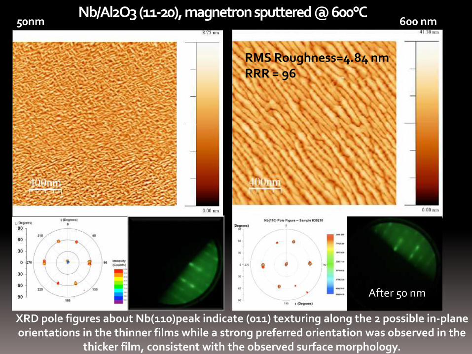
Nb/Al2O3 (11-20), magnetron sputtered @ 600°C50nm
RMS Roughness=4.84 nmRRR = 96
After 50 nm
600 nm
XRD pole figures about Nb(110)peak indicate (011) texturing along the 2 possible in-plane orientations in the thinner films while a strong preferred orientation was observed in the
thicker film, consistent with the observed surface morphology.

Strain Evolution & Structure
In heterostrained growth occurs wherein the film’s lattice spacing deviates from bulk equilibrium values. As the film grows thicker, the strain may be relieved by the formation of lattice defects such as vacancies or dislocations. RHEED(Reflection High Energy Electron Diffraction) is a surface sensitive technique that was used to characterize strain evolution in this case. The niobium lattice parameter at the surface can be determined by analyzing the spacing of the characteristic streaks.
RHEED
•RHEED images were collected for epitaxial niobium for varying thicknesses and growth parameters.•Image processing with MATLAB allows for a systematic way to abstract information related to surface crystallinityand morphology.•A specific image can be used to calculate the lattice parameter corresponding to the top most layer of the sample using the following equation: a*= 2pW/lL•Curve-fitting models are then applied to obtain quantitative information to extract the in-plane strain and lattice parameters
4th International Workshop on thin Films and New Ideas for Pushing the Limits of RF Superconductivity - A-M Valente-Feliciano

Structure vs. bias voltage -Al2O3 (11-20)
Bias [V] 0V -30 -60 -120 -150
Tc [K] 9.10 9.26 9.10 9.2 9.00
DTc [K] 0.08 0.02 0.20 0.04 0.10
RRR 132 141 179.9 179.8 152.6
PF (110) (110) (110) (110) (110)
Orientation spread [°]
0.281 0.244 0.183 0.115 0.161
15mm x 15mm, 0.1mmCI =0.835000x
0.025°Tc
DTc
4th International Workshop on thin Films and New Ideas for Pushing the Limits of RF Superconductivity - A-M Valente-Feliciano

Structure vs. Bake Temperature-Al2O3 (11-20)
Tbake[°C] 360 700 900
Tc [K] 9.20 9.19 9.23
DTc[K] 0.04 0.03 0.02
RRR 179.8 213.3 71.5
PF (110) (110) (110)
Orientation spread [°]
0.115 0.025 3.575
Thickness [nm] 840 1140 270
(Bias -120V)
4th International Workshop on thin Films and New Ideas for Pushing the Limits of RF Superconductivity - A-M Valente-Feliciano

4th International Workshop on thin Films and New Ideas for Pushing the Limits of RF Superconductivity - A-M Valente-Feliciano
ECR, bias -120V, 20 minutes, bake-out (1.5hrs) and coating @450ºC
Nb/c-Al2O3 (0001)
250 x 250 μm, 2 μm resolution, CI Avg. 30

CI =0.24
Sapphire (0001) substrate
0V -60V -150V
0.357 °
CI =0.58
CI =0.20
CI =0.54
CI =0.50
CI =0.69
CI =0.82 0.320° 0.269°
15 0 m
m x
150m
m, 1 m
m ste
p50
0x
500
0x
15 mm
x 15
mm
, 0.1 m
m ste
p
4th International Workshop on thin Films and New Ideas for Pushing the Limits of RF Superconductivity - A-M Valente-Feliciano
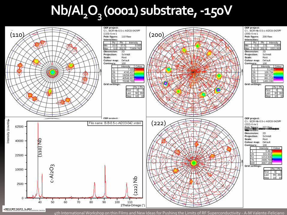
Nb/Al2O3 (0001) substrate, -150VODF project:
C:\...\ECR-Nb-0.5-c-Al2O3-042\PF
(110)-0.rw 1
Pole figure: 110 Raw
Intensities:
Psi Phi Intensity
Min 10.0 57.5 0.000
Max 0.0 352.5 71609.760
Dimension: 2D
Projection: Schmidt
Scale: Root
Colour map: Default
Contours: 100
Intensity Colour
1 7.020
26 4745.437
51 18258.699
76 40546.807
100 70198.765
Grid settings:
Psi Phi
First 0 0
Last 90 360
Step 10 10
ODF project:
C:\...\ECR-Nb-0.5-c-Al2O3-042\PF
(200)-0.rw 1
Pole figure: 200 Raw
Intensities:
Psi Phi Intensity
Min 0.0 2.5 0.000
Max 55.0 202.5 1521.000
Dimension: 2D
Projection: Schmidt
Scale: Root
Colour map: Default
Contours: 100
Intensity Colour
1 0.149
26 100.794
51 387.817
76 861.219
100 1491.030
Grid settings:
Psi Phi
First 0 0
Last 90 360
Step 10 10
ODF project:
C:\...\ECR-Nb-0.5-c-Al2O3-042\PF
(211)-0.rw 1
Pole figure: 211 Raw
Intensities:
Psi Phi Intensity
Min 0.0 52.5 0.000
Max 20.0 207.5 4096.000
Dimension: 2D
Projection: Schmidt
Scale: Root
Colour map: Default
Contours: 100Intensity Colour
1 0.402
26 271.434
51 1044.378
76 2319.233
100 4015.293
Grid settings:
Psi Phi
First 0 0
Last 90 360
Step 10 10
ODF project:
C:\...\ECR-Nb-0.5-c-Al2O3-042\PF
(222)-0.rw 1
Pole figure: 222 Raw
Intensities:Psi Phi Intensity
Min0.0 172.5 0.000
Max0.0 317.5 4761.000
Dimension: 2D
Projection: Schmidt
Scale: Root
Colour map: Default
Contours: 100
Intensity Colour
1 0.467
26 315.502
51 1213.936
76 2695.769
100 4667.189
Grid settings:
Psi Phi
First 0 0
Last 90 360
Step 10 10
40 50 60 70 80 90 100 1102Theta-Omega (°)
0
2500
10000
22500
40000
62500
Inte
nsity (
counts
)
(110
) Nb
c-A
l2O
3
(222
) Nb
(110) (200)
(222)
4th International Workshop on thin Films and New Ideas for Pushing the Limits of RF Superconductivity - A-M Valente-Feliciano

Structure vs. bias voltage -Al2O3 (0001)Bias [V] 0 -30 -60 -120 -150
Tc [K] 8.85 9.21 9.28 9.24 9.22
DTc[K] 0.1 0.02 0.04 0.02 0.05
RRR 84 51 108 100 76
PF (111) (111) (111) (110) (110)
Thickness [nm] 0.88 1.02 1.33 1.14 0.53
Tc
DTc
4th International Workshop on thin Films and New Ideas for Pushing the Limits of RF Superconductivity - A-M Valente-Feliciano

Nb epitaxy on Al2O3
Nb films deposited with higher bias voltages on (0001) sapphire grow along (110) not (111) as anticipated.Due to higher ion incident energy? T. Wagner et al., J. Mat. Res. Vol. 11, nº5, pp. 1255-1264 (1996), Mat. Res. Symp. Proc, Vol. 440, pp.151-156, (1997)MBE Nb films on (0001) sapphire grow along (111) at 900°C, but (110) at 1100°C
I n all cases, Nb films grow along (110) on a-plane sapphire (11-20) for both magnetron sputtered film s and ECR films with different bias voltages.
RRR values from 8 to 213 have been obtained by varying the incident ion energy with a bias voltage, the cleanliness of the interface and ad-mobility of the atoms on the surface with baking and coating substrate temperatures.
4th International Workshop on thin Films and New Ideas for Pushing the Limits of RF Superconductivity - A-M Valente-Feliciano
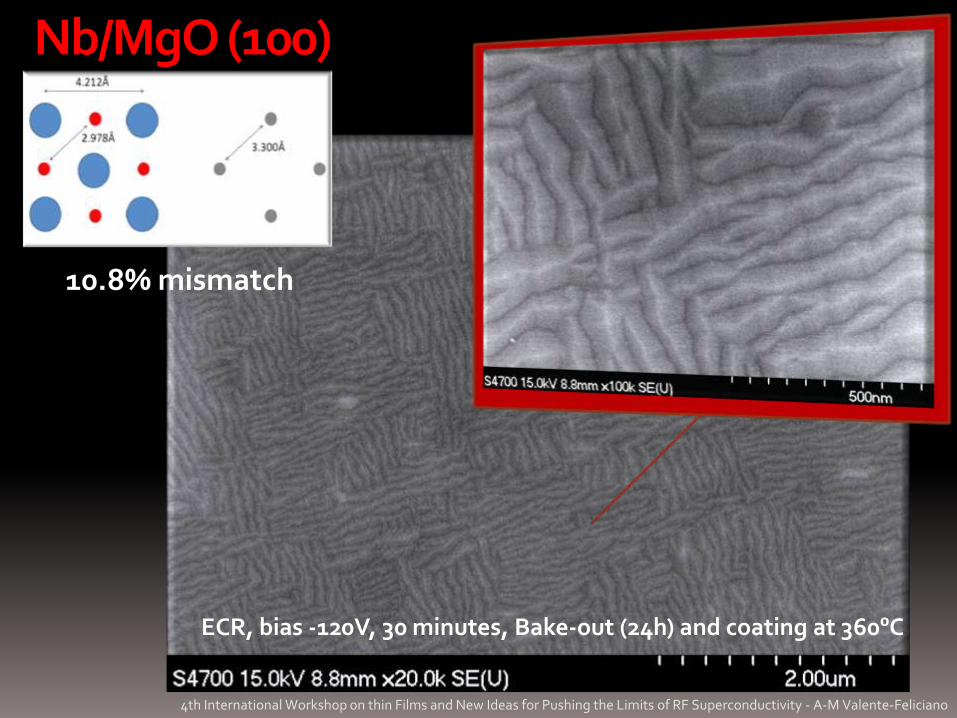
Nb/MgO (100)
ECR, bias -120V, 30 minutes, Bake-out (24h) and coating at 360ºC
10.8% mismatch
4th International Workshop on thin Films and New Ideas for Pushing the Limits of RF Superconductivity - A-M Valente-Feliciano
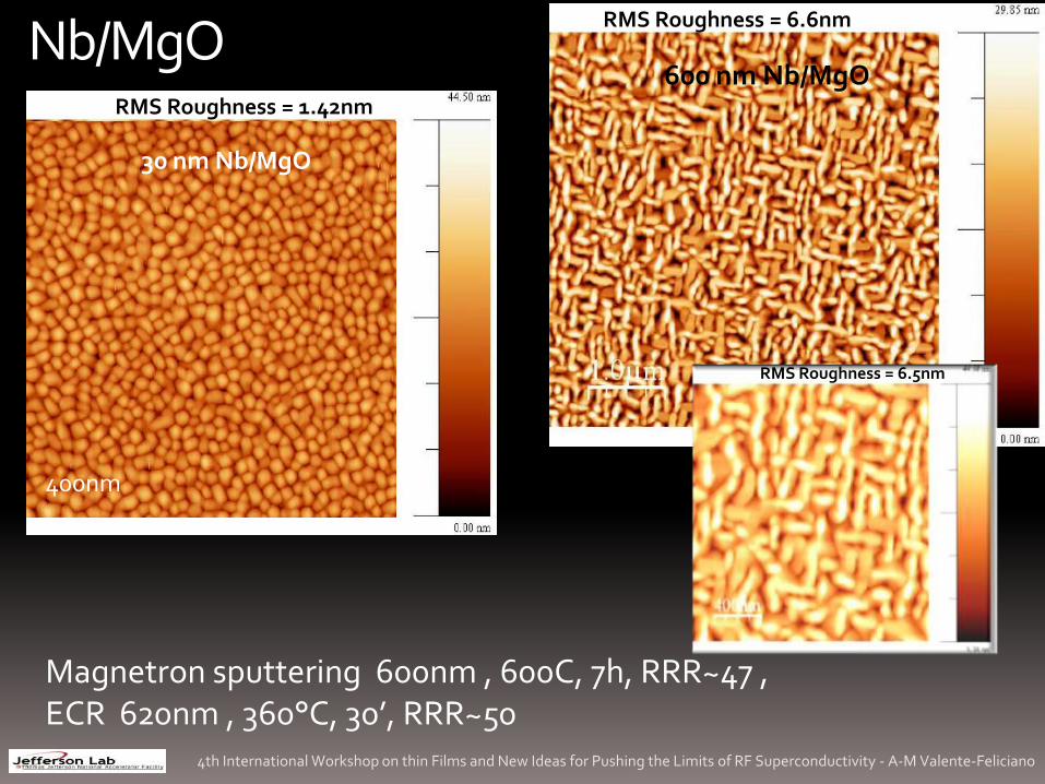
RMS Roughness = 6.6nm
Nb/MgO
RMS Roughness = 6.5nm
RMS Roughness = 1.42nm
30 nm Nb/MgO
600 nm Nb/MgO
400nm
Magnetron sputtering 600nm , 600C, 7h, RRR~47 , ECR 620nm , 360°C, 30’, RRR~50
4th International Workshop on thin Films and New Ideas for Pushing the Limits of RF Superconductivity - A-M Valente-Feliciano

150 mm x 150mm, 1mm step500x
-150V
0.173°
-120V
75mm x 75mm, 1mmCI =0.161000x
0V -60V
CI =0.28
-30V
4th International Workshop on thin Films and New Ideas for Pushing the Limits of RF Superconductivity - A-M Valente-Feliciano
CI =0.42CI =0.19 CI =0.2
Nb/MgO (100)
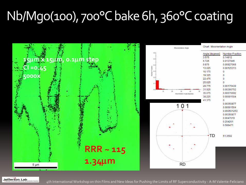
Nb/Mgo(100), 700°C bake 6h, 360°C coating
15mm x 15mm, 0.1mm stepCI =0.455000x
RRR ~ 1151.34mm
4th International Workshop on thin Films and New Ideas for Pushing the Limits of RF Superconductivity - A-M Valente-Feliciano

Structure vs. bias voltage MgO(100)Bias 0V -30V -60 -90 -120 -150
Tc [K] 9.1 0.37 9.2 9.36 9.20 9.05
DTc 0.11 0.01 0.04 0.04 0.09 0.20
RRR 33 51 59 44 81 50
PF (110) (110) (110) (110) (110) (110)
Thickness [mm] 0.34 0.51 0.94 1.17 1.26 0.62
Tc
DTc
4th International Workshop on thin Films and New Ideas for Pushing the Limits of RF Superconductivity - A-M Valente-Feliciano
Nb growth on MgO
I n all cases, Nb films grow along (110) on MgO (110) for both magnetron sputtered films and ECR films with different bias voltages.
Despite a large lattice mismatch, RRR values up to 115 have been obtained by varying the incident ion energy, the baking and coating substrate temperatures.
4th International Workshop on thin Films and New Ideas for Pushing the Limits of RF Superconductivity - A-M Valente-Feliciano

Nb/Cu
ECR, bias -120V, 20 minutes, Bake-out (18hrs) and coating at 450ºC
4th International Workshop on thin Films and New Ideas for Pushing the Limits of RF Superconductivity - A-M Valente-Feliciano

Single crystal Cu substrates
(100) (110) (111)
0.733° 0.357 ° 0.432°
CI =0.58CI =0.59CI =0.51
50x 1500 mm x 1500mm, 25 mm step
Lattice mismatch with(100) 8.5%
4th International Workshop on thin Films and New Ideas for Pushing the Limits of RF Superconductivity - A-M Valente-Feliciano

150mm x 150mm, 1mmCI =0.49500x
15mm x 15mm, 0.1mmCI =0.245000x
15mm x 15mm, 0.1mmCI =0.065000x
150mm x 150mm, 1mmCI =0.24500x
150mm x 150mm, 1mmCI =0.21500x
15mm x 15mm, 0.1mmCI =0.785000x
Nb(110)//Cu(100) Nb(100)//Cu(110) (Nb(110)//Cu(111)
Nb hetero-epitaxy on Cu
4th International Workshop on thin Films and New Ideas for Pushing the Limits of RF Superconductivity - A-M Valente-Feliciano

150 mm x 150mm
Nb/Cu (100)
CI =0.46
CI =0.53
CI =0.28
Nb/Cu (111)
Nb/Cu (110)
-150V
1000mm x 1000mm, 50mmCI =0.1500x
150mm x 150mm, 1mmCI =0.09500x
15mm x 15mm, 0.1mmCI =0.275000x
150mm x 150mm, 1mmCI =0.14500x
-120V-60V-0V
150 mm x 150mmCI =0.34500x
CI =0.11
CI =0.12
4th International Workshop on thin Films and New Ideas for Pushing the Limits of RF Superconductivity - A-M Valente-Feliciano

Nb/Cu2O – High Resolution TEM
4th International Workshop on thin Films and New Ideas for Pushing the Limits of RF Superconductivity - A-M Valente-Feliciano

Effect of Bias Voltage for Nb/Cu2O
Obvious advantage: no noble gas for plasma creation
Sample tests: good RRR and Tc, 100-nm grain size, lower defect density and smooth surfaces
60eV
90eV 4000X4000 µm2
3-D Profilometer ImagesTEM Images
20 30 40 50 60 70 80 90 100 110
0
5000
10000
15000
20000
Inte
nsity)
2 theta
110 Nb
200 Cu
211 Nb 220 Nb311 Cu
NbOx
Sample: JLAB-ECR-028B
20 30 40 50 60 70 80 90 100 110
-2000
0
2000
4000
6000
8000
10000
12000
14000
16000
Inte
nsity
2 theta
110 Nb
200 Cu
220 Nb 311 Cu211 Nb
111 Cu
NbOx
Sample:JLAB-ECR-026A
200 Nb 220Cu
4th International Workshop on thin Films and New Ideas for Pushing the Limits of RF Superconductivity - A-M Valente-Feliciano
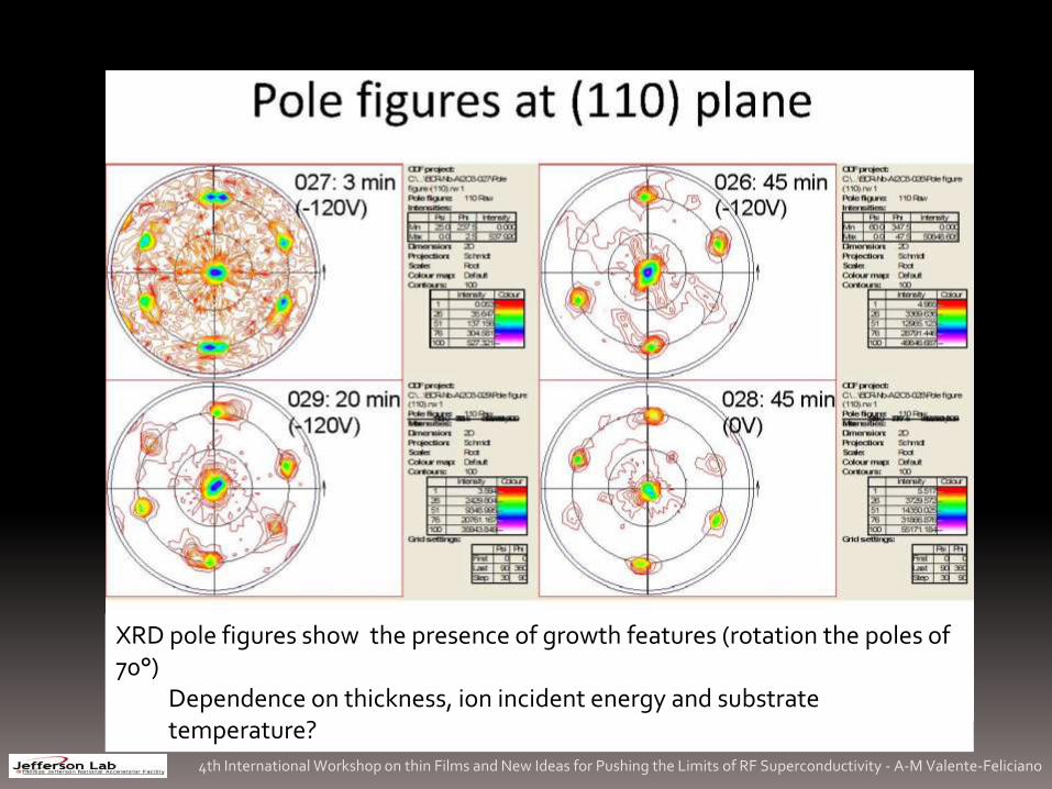
XRD pole figures show the presence of growth features (rotation the poles of 70°)
Dependence on thickness, ion incident energy and substrate temperature?
4th International Workshop on thin Films and New Ideas for Pushing the Limits of RF Superconductivity - A-M Valente-Feliciano

Nb/Cu – High Resolution TEM
4th International Workshop on thin Films and New Ideas for Pushing the Limits of RF Superconductivity - A-M Valente-Feliciano

150 x 150 μm, 1 μm resolution,CI Avg. 0.71
120 x 150 μm, 1 μm resolution,CI Avg. 0.23
50 x 75 μm, 1 μm resolution,CI Avg. 0.16
Bias -120V, 2mm Bias 0V , 4mm
Typical Cu substrate
Effect of Bias Voltage for Nb/Cu

Nb/Cu, fine grain – effect of Bias voltage
750mm x 750mm, 10mmCI =0.04100x
CI =0.05
-30V-60V -90V
-120V -150V
CI =0.25
150mm x 150mm, 1mm step500x
CI =0.32
CI =0.2CI =0.11
4th International Workshop on thin Films and New Ideas for Pushing the Limits of RF Superconductivity - A-M Valente-Feliciano
Ab-normal growth
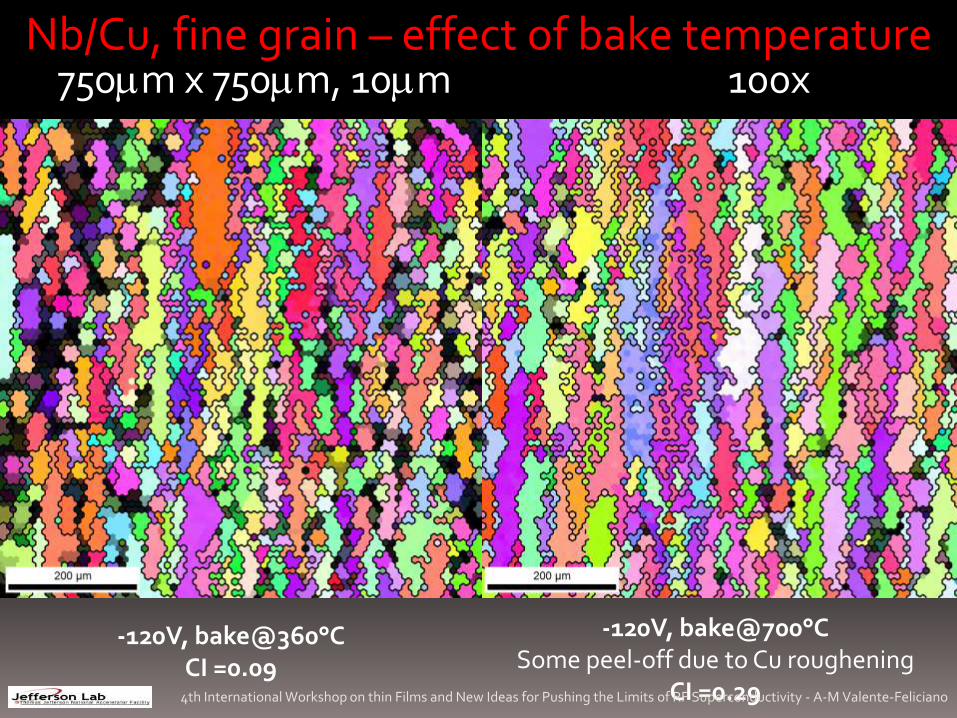
750mm x 750mm, 10mm 100x
-120V, bake@360°CCI =0.09
-120V, bake@700°CSome peel-off due to Cu roughening
CI =0.29
Nb/Cu, fine grain – effect of bake temperature
4th International Workshop on thin Films and New Ideas for Pushing the Limits of RF Superconductivity - A-M Valente-Feliciano

Nb/Cu, large grain
CI =0.22
-30V -120V
-150V
750mm x 750mm, 10mm step100x
CI =0.2
CI =0.26
1500 mm x 1500 mm, 10mm step50x
4th International Workshop on thin Films and New Ideas for Pushing the Limits of RF Superconductivity - A-M Valente-Feliciano
Equi-axial growthTo be verified by cross-sectionEBSD

1st SIC Measurements on Nb/Cu2O & Cu
4th International Workshop on thin Films and New Ideas for Pushing the Limits of RF Superconductivity - A-M Valente-Feliciano
Nb growth on Cu substratesHetero-epitaxial relationship between Nb and Cu have been verified with ECR.
Films have been grown on both oxidized and metallic Cu surfaces.As a function of the bias voltage and substrate temperature, it appears that the film structure can be tailored from columnar growth to equi-axial growth in the case of epitaxy. Cross-section observation with EBSD and TEM are necessary to establish it.RRR measurements on films grown on Cu need to be performed for direct correlation with RF measurements
4th International Workshop on thin Films and New Ideas for Pushing the Limits of RF Superconductivity - A-M Valente-Feliciano

CONCLUDING REMARKSJLab in collaboration with surrounding universities (College William & Mary, Old Dominion University and Norfolk State University) is pursuing two opportunities to create viable superconducting RF cavity surfaces to reduce the cost framework of SRF accelerators and to reach higher gradients and allow operation of SRF structures at 4K.
One of them is to understand and develop niobium films with bulk-like performance by elucidating the functional dependence of film-grown Nb crystal texture, intra-grain defect density, and grain boundary impurities on SRF performance. Studies on the correlation of the surface resistance of films produced by energetic condensation ECR with surface and material properties of the film as a function of incident ion energy and substrate temperature are underway.
Nb films have been grown on a variety of substratesHigh RRR values have been achieved on Al2O3 and MgO substrates.
The Nb film structure can be tuned from columnar growth, ab-normal to equi-axial growth by varying the incident ion energy with the substrate temperature for temperatures lower than if using thermal energy only.
4th International Workshop on thin Films and New Ideas for Pushing the Limits of RF Superconductivity - A-M Valente-Feliciano

SRF Thin Films Collaboration
Under DOE HEP Grant ARRA & U.S. DOE Contract No. DE-AC05-06OR23177
Films creation:Jlab: A-M Valente-Feliciano, J. Spradlin, L. PhillipsW&M: A. Lukaszew, D. Beringer, S. ….
Material and RF characterization:Jlab: A-M Valente-Feliciano, J. Spradlin, L. Phillips, X. Zhao, B. Xiao, A. WuW&M: A. Lukaszew, D. Beringer, S. , R. Outlaw, O. TrofimovaNSU: K. SeoODU: H. Baumgart, D. GuBlack Labs LLC: R. Crooks
4th International Workshop on thin Films and New Ideas for Pushing the Limits of RF Superconductivity - A-M Valente-Feliciano
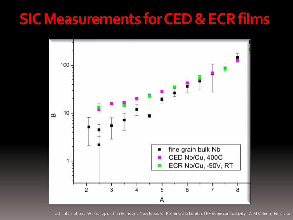
SIC Measurements for CED & ECR films
4th International Workshop on thin Films and New Ideas for Pushing the Limits of RF Superconductivity - A-M Valente-Feliciano

Cu thermal roughening
50mm x 50mmZ Range = 1.694 µm
RMS = 203.79 nmRa = 156.50 nm
Z Range = 241.08 nmRMS = 22.568 nm
Ra = 18.114 nm
4th International Workshop on thin Films and New Ideas for Pushing the Limits of RF Superconductivity - A-M Valente-Feliciano
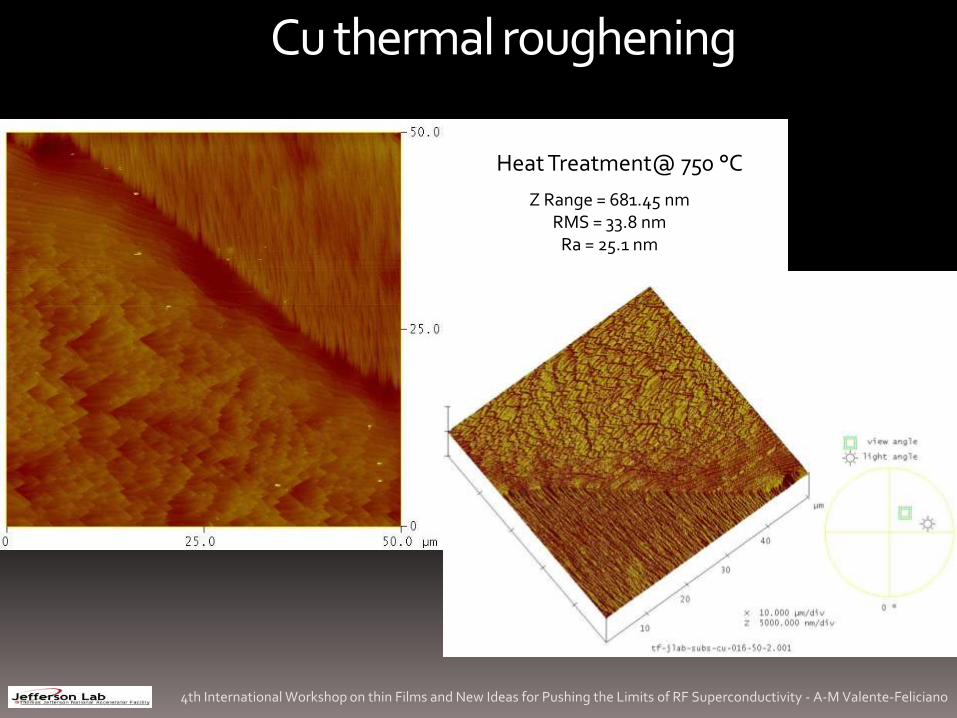
Cu thermal roughening
Heat Treatment@ 750 °C
Z Range = 681.45 nmRMS = 33.8 nm
Ra = 25.1 nm
4th International Workshop on thin Films and New Ideas for Pushing the Limits of RF Superconductivity - A-M Valente-Feliciano

Sample 018 – Heat Treated 450 °C Sample 016 – Heat Treated 750 °C
4th International Workshop on thin Films and New Ideas for Pushing the Limits of RF Superconductivity - A-M Valente-Feliciano

NbTiN, NbN, Mo3Re, V3Si coatingswith Reactive Sputtering and
High Power Pulse Magnetron Sputtering& MgO, AlN, Al2O3 coating with reactive, RF sputtering
New UHV Multi-technique deposition system under commissioning @ JLab
A unique, versatile thin film deposition system enabling multiple coating techniques in-situ
Designed to enable rapid exploration of the production parameter space of:
Nb filmsAlternative material films like NbN, NbTiNS-I-S multilayer structures based on these compounds

Thin Films: Alternative Materials
4th International Workshop on thin Films and New Ideas for Pushing the Limits of RF Superconductivity - A-M Valente-Feliciano

Alternative Materials:
NbTiN, NbNNb3Sn, V3Si, Mo3Re
Substrates :
Single crystal NbPoly crystalline NbThick Nb/Cu films
Insulator:
Al2O3, MgO, AlNAccording to
lattice mismatch between
I and S materials
Multilayer:S/I/Nb & S/I/S/I/…/S/I/Nb
Study of growth modes of Superconductor/ Insulator
&Insulator/superconductor
Multilayers & Alternative Materials
4th International Workshop on thin Films and New Ideas for Pushing the Limits of RF Superconductivity - A-M Valente-Feliciano

3D Epitaxial Relationship of Nb and a-plane Sapphire
Note: Twoequivalents both satisfy “3D-Registry”
Nb [111]
Al2O3 [0001]
1800
[100]
[010]
Nb (011)
Nb* (011)
[001]
[1010]
[101]
Nb (0,1,-1) // Al2O3(1,1,-2,0)
Nb [1,1,1] // Al2O3 [0001]
Nb [1,0,-1] // Al2O3[1,0,-1,0]
4th International Workshop on thin Films and New Ideas for Pushing the Limits of RF
Superconductivity - A-M Valente-Feliciano

IPF from Plane Normal [001] IPF from Transverse Direction [010]Nb/MgO (100)
62 °/<773>
~90° / <101>
(IPF from Transverse Direction [010])
4th International Workshop on thin Films and New Ideas for Pushing the Limits of RF Superconductivity - A-M Valente-Feliciano

SRF Cavities: state of the art
Breakdown fields close to the de-pairing limit of 50 MV/m for NbBest Nb cavities approaching their intrinsic limit at Hmax = HC
Nb has the highest Tc among all pure metals and the highest Hc1≈150 mT among all superconductorsMeissner state can exist up to H = Hc
4th International Workshop on thin Films and New Ideas for Pushing the Limits of RF Superconductivity - A-M Valente-Feliciano

Thin Films: niobium –state of the art
Attaining even bulk-like performance with Nb film would enable
major system simplifications.
Deposited films, once a production process is developed, may offer
the highest level of quality assurance and
thus reliable performance.
1.5 GHz Nb/Cu cavities, sputtered w/ Krat 1.7 K (Q0=295/Rs)
Nb
Nb/Cu
• The maximum field of Nb/Cu cavities is not limited by anyintrinsic phenomena.
• However, the residual resistance suffers from a steepincrease at high field (threshold ~15 MV/m).
• Several possible causes have been investigated. The mostprobable sources are: surface defects, hydrogen content.
CERN 2000
4th International Workshop on thin Films and New Ideas for Pushing the Limits of RF Superconductivity - A-M Valente-Feliciano

Thin Films applications:Nb, Alternative Materials & Multilayers
Use of SRF Thin Films
Bulk Nb Nb film (>1mm thick)
Multi-LayersS-I-S-I-S
SubstrateSubstrateCu, Al …
Single LayerNb, high k
Bulk-like performance Nb film major system simplifications.highest level of quality assurance and reliable performance.Use of substrates with higher thermal conductivity
NbN, Nb3Sn, MgB2, S-I-S-I-S…
Accessible almost only via deposited or synthesized films.
high k superconducting filmsfunction at higher temperatures or higher fields Suppression of vortex entry in multilayer structures
for cavity operation at 4.2K or higher
4th International Workshop on thin Films and New Ideas for Pushing the Limits of RF Superconductivity - A-M Valente-Feliciano


![Auditoria valente 1[1][1] (1)](https://static.fdocuments.us/doc/165x107/546eaf74b4af9faf268b475c/auditoria-valente-111-1.jpg)