Vacuum Fluorescent Display Module - Allied Electronics · 2.2 Since a DC/DC converter is used, ......
11
M0116MY‐161LSBR2‐S2 Vacuum Fluorescent Display Module RoHS Compliant Newhaven Display International, Inc. 2511 Technology Drive, Suite 101 Elgin IL, 60124 Ph: 847‐844‐8795 Fax: 847‐844‐8796 www.newhavendisplay.com [email protected] [email protected]
Transcript of Vacuum Fluorescent Display Module - Allied Electronics · 2.2 Since a DC/DC converter is used, ......
M0116MY‐161LSBR2‐S2 Vacuum Fluorescent Display Module
RoHS Compliant
Newhaven Display International, Inc. 2511 Technology Drive, Suite 101 Elgin IL, 60124 Ph: 847‐844‐8795 Fax: 847‐844‐8796
www.newhavendisplay.com [email protected] [email protected]
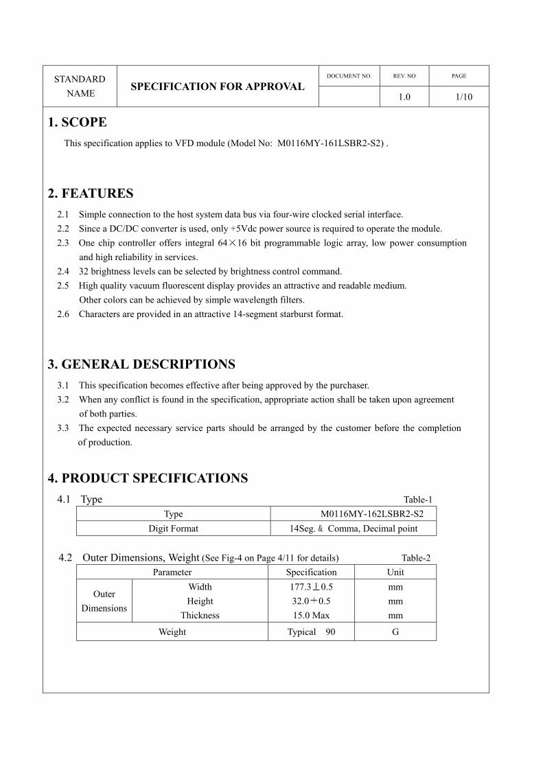
DOCUMENT NO. REV. NO PAGE STANDARD NAME
SPECIFICATION FOR APPROVAL 1.0 1/10
1. SCOPE This specification applies to VFD module (Model No: M0116MY-161LSBR2-S2) .
2. FEATURES 2.1 Simple connection to the host system data bus via four-wire clocked serial interface. 2.2 Since a DC/DC converter is used, only +5Vdc power source is required to operate the module. 2.3 One chip controller offers integral 64 16 bit programmable logic array, low power consumption
and high reliability in services. 2.4 32 brightness levels can be selected by brightness control command. 2.5 High quality vacuum fluorescent display provides an attractive and readable medium.
Other colors can be achieved by simple wavelength filters. 2.6 Characters are provided in an attractive 14-segment starburst format.
3. GENERAL DESCRIPTIONS 3.1 This specification becomes effective after being approved by the purchaser. 3.2 When any conflict is found in the specification, appropriate action shall be taken upon agreement
of both parties. 3.3 The expected necessary service parts should be arranged by the customer before the completion
of production.
4. PRODUCT SPECIFICATIONS 4.1 Type Table-1
Type M0116MY-162LSBR2-S2 Digit Format 14Seg. & Comma, Decimal point
4.2 Outer Dimensions, Weight (See Fig-4 on Page 4/11 for details) Table-2
Parameter Specification Unit
Outer Dimensions
Width Height
Thickness
177.3 0.5 32.0 0.5 15.0 Max
mm mm mm
Weight Typical 90 G
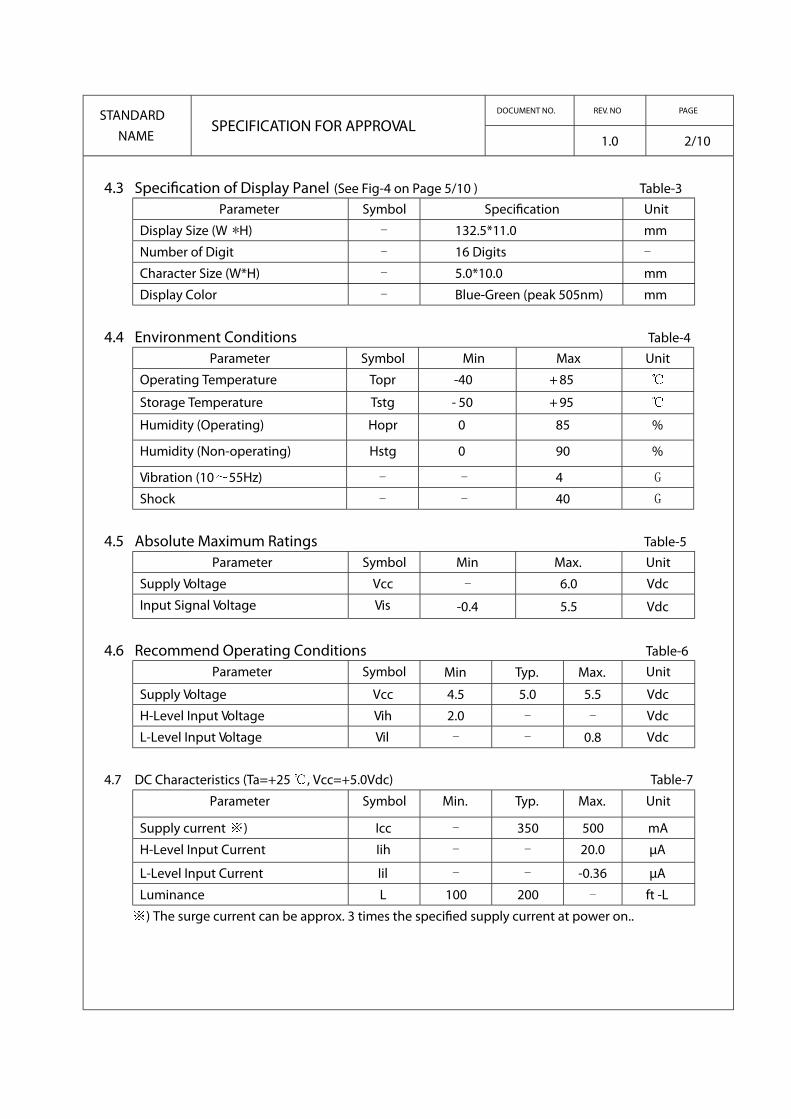
DOCUMENT NO. REV. NO PAGE STANDARD NAME
SPECIFICATION FOR APPROVAL 1.0 2/10
4.3 Speci�cation of Display Panel (See Fig-4 on Page 5/10 ) Table-3 Parameter Symbol Speci�cation Unit
Display Size (W *H) - 132.5*11.0 mm
Number of Digit - 16 Digits -
Character Size (W*H) - 5.0*10.0 mm
Display Color - Blue-Green (peak 505nm) mm
4.4 Environment Conditions Table-4
Parameter Symbol Min Max Unit
Operating Temperature Topr -40 + 85
Storage Temperature Tstg - 50 + 95
Humidity (Operating) Hopr 0 85 %
Humidity (Non-operating) Hstg 0 90 %
Vibration (10 55Hz) - - 4 G
Shock - - 40 G
4.5 Absolute Maximum Ratings Table-5 Parameter Symbol Min Max. Unit
Supply Voltage Vcc - 6.0 Vdc
Input Signal Voltage Vis -0.4 5.5 Vdc
4.6 Recommend Operating Conditions Table-6 Parameter Symbol Min Typ. Max. Unit
Supply Voltage Vcc 4.5 5.0 5.5 Vdc
H-Level Input Voltage Vih 2.0 - - Vdc
L-Level Input Voltage Vil - - 0.8 Vdc
4.7 DC Characteristics (Ta=+25 , Vcc=+5.0Vdc) Table-7
Parameter Symbol Min. Typ. Max. Unit
Supply current ) Icc - 350 500 mA
H-Level Input Current Iih - - 20.0 µA
L-Level Input Current Iil - - -0.36 µA
Luminance L 100 200 - ft -L
) The surge current can be approx. 3 times the speci�ed supply current at power on..
DOCUMENT NO. REV NO PAGE STNDARD NAME
SPECIFICATION FOR APPROVAL 1.0 3/10
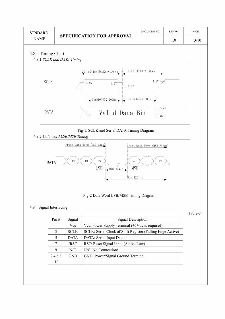
4.8 Timing Chart
4.8.1 SCLK and DATA Timing
DATA
SCLK
20 s Ton(SCLK) 1.0 s Toff(SCLK) 1.0 s
4.2V 4.2V4.2V
1.0V
Tsu(DATA) 200ns TH(DATA) 100ns
Valid Data Bit4.2V
1.0V
Fig-1. SCLK and Serial DATA Timing Diagram
4.8.2 Data word LSB/MSB Timing
Prior Data Word (LSB Last) Next Data Word (MSB First)
D0D7D0D1D2DATA
Min 120 s
Min 40 sLSB MSB
Fig-2 Data Word LSB/MSB Timing Diagram
4.9 Signal Interfacing Table-8
Pin # Signal Signal Description 1 Vcc Vcc: Power Supply Terminal (+5Vdc is required) 3 SCLK SCLK: Serial Clock of Shift Register (Falling Edge Active) 5 DATA DATA: Serial Input Data
7 /RST RST: Reset Signal Input (Active Low) 9 N/C N/C: No Connection/
2,4,6,8,10
GND GND: Power/Signal Ground Terminal
DOCUMENT NO. REV. NO PAGE STNDARD NAME
SPECIFICATION FOR APPROVAL 1.0 4/10
4.10 System Block Diagram
SCLK
DATA
VDD
POR
VSS
Grids
Anodes
F1
F2
VFD
-VdisDC/DC Converter Circuit
Controller
16*Rg
16*Ra
-Vdis
-Vdis
Vcc
Vcc
Rupx3
16
16
SCLK
DATA
/RST
Vcc
GND
(+5Vdc)
Fig-3 VFD Module System Block Diagram
4.11 Outer Dimensions
Fig-4. Outer Dimensions

DOCUMENT NO. REV. NO PAGE STNDARD NAME
SPECIFICATION FOR APPROVAL 1.0 5/10
5. FUNCTIONS The module has control data, display data write and reset functions. Input data from the host system is loaded into the module’s display buffer via the serial data input channel as
8-bit serial data. The MSB value of 8-bit serial data determines whether the input data into this module is control data or display data.
TIME First Input Last Input
DATA MSB LSB
SCLK
Fig-5 Synchronous Serial Data Input . 5.1 Control Data
The control data can be input by setting MSB to “1” : In addition, a command type and associated data with the command is determined by the D6 D0.
Binary Code Command Function
D7 D6 D5 D4 D3 D2 D1 D0 Buffer Pointer Control Specifies the RAM address. 1 0 1 0 23 22 21 20 Digit Counter Control Sets the number of digits. 1 1 0 0 23 22 21 20 Brightness Control Sets the brightness. 1 1 1 24 23 22 21 20
D7 D1D2D3D4D5D6 D0

DOCUMENT NO. REV.NO PAGE STNDARD NAME
SPECIFICATION FOR APPROVAL 1.0 6/10
5.1.1 Buffer Pointer Control
This command changes the display contents only at an arbitrary digit. (The RAM write address is set.) The digit position to be modified is represented by the value of D3 D0. If the most significant digit(left-end digit) is to be selected, each of D3 D0 are set to a value of “1” and if the second digit is to be selected ,each of D3 D3 set to a value of “0”. Otherwise a decimal value of from “1”to “12” should be entered. The set value of D3 D0 is lower than the decimal value of the specified position by 2.
Table-10 Binary Code Binary Code
Digit D
7
D
6
D
5
D
4
D
3
D
2
D
1
D
0
Digit D
7
D
6
D
5
D
4
D
3
D
2
D
1
D
0
Left End 1 0 1 0 1 1 1 1 9th 1 0 1 0 0 1 1 1
2nd 1 0 1 0 0 0 0 0 10th 1 0 1 0 1 0 0 0
3rd 1 0 1 0 0 0 0 1 11th 1 0 1 0 1 0 0 1
4th 1 0 1 0 0 0 1 0 12th 1 0 1 0 1 0 1 0
5th 1 0 1 0 0 0 1 1 13th 1 0 1 0 1 0 1 1
6th 1 0 1 0 0 1 0 0 14th 1 0 1 0 1 1 0 0
7th 1 0 1 0 0 1 0 1 15th 1 0 1 0 1 1 0 1
8th 1 0 1 0 0 1 1 0 Right End 1 0 1 0 1 1 1 0
5.1.2 Digit Counter Control
This command is used to define the number of display digits. The code is normally used only during initialization routine of the host system. If all 13 characters are to be controlled, each of D3 D0 are set to a value of “0”, otherwise a decimal value from “1” to “12” is entered, corresponding to the actual number of characters to be controlled.
Table-11 Binary Code Binary Code Number of
Display
Digit D
7
D
6
D
5
D
4
D
3
D
2
D
1
D
0
Number of
Display
Digit D
7
D
6
D
5
D
4
D
3
D
2
D
1
D
0
1 1 1 0 0 0 0 0 1 9 1 1 0 0 1 0 0 1
2 1 1 0 0 0 0 1 0 10 1 1 0 0 1 0 1 0
3 1 1 0 0 0 0 1 1 11 1 1 0 0 1 0 1 1
4 1 1 0 0 0 1 0 0 12 1 1 0 0 1 1 0 0
5 1 1 0 0 0 1 0 1 13 1 1 0 0 1 1 0 1
6 1 1 0 0 0 1 1 0 14 1 1 0 0 1 1 1 0
7 1 1 0 0 0 1 1 1 15 1 1 0 0 1 1 1 1
8 1 1 0 0 1 0 0 0 16 1 1 0 0 0 0 0 0

DOCUMENT NO. REV.NO PAGE STNDARD NAME
SPECIFICATION FOR APPROVAL 1.0 7/10
5.1.3 Brightness Control
This command sets the brightness of the VFD. This command allows the brightness to be adjusted by 1/32 step. As shown in Table-12, the test value ranges from 0 to 31.
Table-12 Binary Code Binary Code
Brightness
Level D
7
D
6
D
5
D
4
D
3
D
2
D
1
D
0
Brightness
Level D
7
D
6
D
5
D
4
D
3
D
2
D
1
D
0
0/31(0.0%) 1 1 1 0 0 0 0 0 16/31(51.6%) 1 1 1 1 0 0 0 0
1/31(3.2%) 1 1 1 0 0 0 0 1 17/31(54.8%) 1 1 1 1 0 0 0 1
2/31(6.4%) 1 1 1 0 0 0 1 0 18/31(58.1%) 1 1 1 1 0 0 1 0
3/31(9.7%) 1 1 1 0 0 0 1 1 19/31(61.2%) 1 1 1 1 0 0 1 1
4/31(12.9%) 1 1 1 0 0 1 0 0 20/31(64.5%) 1 1 1 1 0 1 0 0
5/31(16.1%) 1 1 1 0 0 1 0 1 21/31(67.7%) 1 1 1 1 0 1 0 1
6/31(19.4%) 1 1 1 0 0 1 1 0 22/31(71.0%) 1 1 1 1 0 1 1 0
7/31(22.6%) 1 1 1 0 0 1 1 1 23/31(74.2%) 1 1 1 1 0 1 1 1
8/31(25.8%) 1 1 1 0 1 0 0 0 24/31(77.4%) 1 1 1 1 1 0 0 0
9/31(29.0%) 1 1 1 0 1 0 0 1 25/31(80.6%) 1 1 1 1 1 0 0 1
10/31(32.3%) 1 1 1 0 1 0 1 0 26/31(83.9%) 1 1 1 1 1 0 1 0
11/31(35.5%) 1 1 1 0 1 0 1 1 27/31(87.1%) 1 1 1 1 1 0 1 1
12/31(38.7%) 1 1 1 0 1 1 0 0 28/31(90.3%) 1 1 1 1 1 1 0 0
13/31(41.9%) 1 1 1 0 1 1 0 1 29/31(93.5%) 1 1 1 1 1 1 0 1
14/31(45.2%) 1 1 1 0 1 1 1 0 30/31(96.8%) 1 1 1 1 1 1 1 0
15/31(48.4%) 1 1 1 0 1 1 1 1 31/31(100%) 1 1 1 1 1 1 1 1
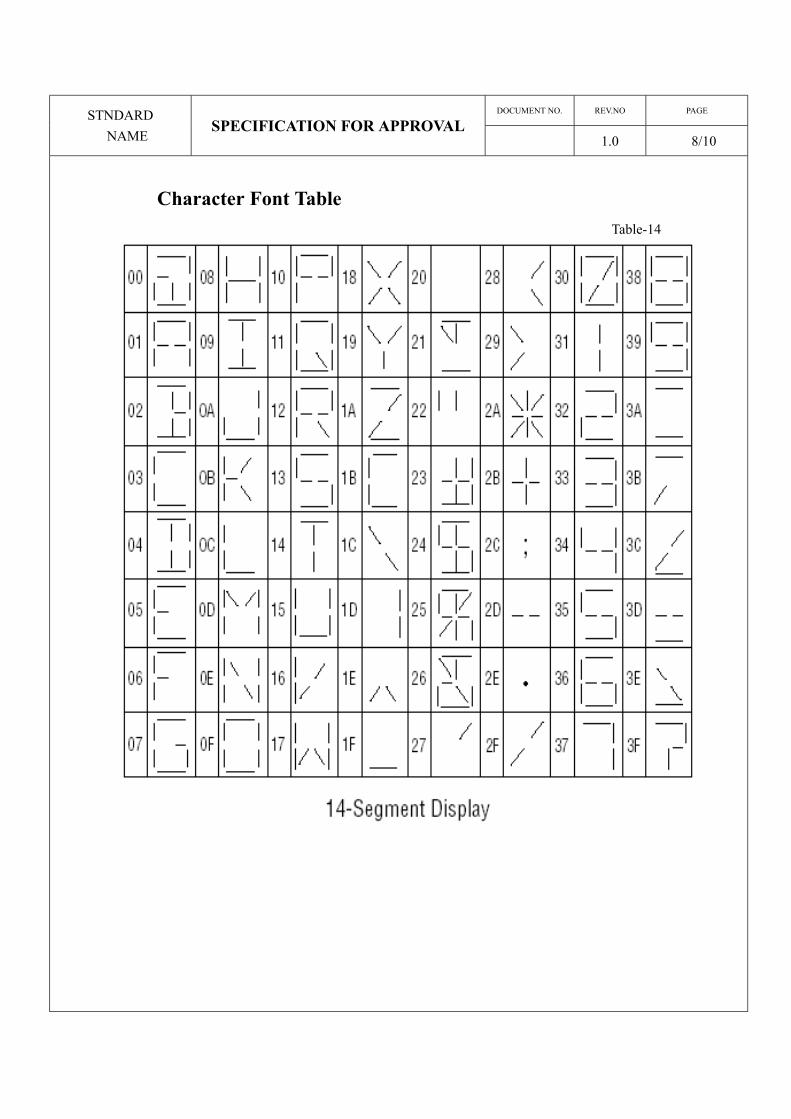
5.2 Input Display Data Word
Display data words are loaded into the display buffer of module as 8-bit codes, with the MSB set to “0”. The 64 available codes are shown in Table-13 on next page. 16 display data words must be entered to fully load the display data buffer. The display buffer pointer (write in position) specified by the buffer. Pointer control command is automatically incremented by one each time the display data is entered. To set the comma or decimal point, the display data codes of 2C Hex or 2E Hex is entered respectively. Only when 2C Hex and 2E Hex data are entered, the display buffer pointer in the RAM is not automatically incremented but stays present location.
DOCUMENT NO. REV.NO PAGE STNDARD NAME
SPECIFICATION FOR APPROVAL 1.0 8/10
Character Font Table
Table-14

DOCUMENT NO. REV. NO PAGE STNDARD NAME
SPECIFICATION FOR APPROVAL 1.0 9/10
5.3 RESET
The reset function allows the users to re-initialize the alphanumeric display controller, while the power is still applied to the module, by applying a logical “0” to pin #5 and pin #7(/RST) of the connector. (Pulse Width≥200us) When the controller is initialized, the display status is shown in Table-13. The RAM data (Display Buffer Data) are the same as the prior data. Table-13
Binary Code Parameter Reset Status
D7 D6 D5 D4 D3 D2 D1 D0 Write in Position Left End Digit 1 0 1 0 1 1 1 1 Number of Display Digit 16 Digits 1 1 0 0 0 0 0 0 Brightness Level 0% 1 1 1 0 0 0 0 0
DOCUMENT NO. REV.NO PAGE TNDARD NAME
SPECIFICATION FOR APPROVAL 1.0 10/10
6. OPERATING RECOMMENDATIONS 6.1 Avoid applying excessive shock or vibration beyond the specification for the VFD module. 6.2 Since VFD is made of glass material, careful handling is required. 6.3 When mounting the VFD module to your system, leave a slight gap between the VFD glass and your front panel.
The module should be mounted without stress to avoid flexing of the PCB. 6.4 Avoid plugging or unplugging the interface connection with the power on, otherwise it may cause
severe damage to input circuitry. 6.5 Slow starting power supply may cause non-operation because one chip Mi-com won’t be reset. 6.6 Exceeding any of maximum ratings may cause the permanent damage. 6.7 Since the VFD module contain high voltage source, careful handling is required while power is on. 6.8 When the power is turned off, the capacitor does not discharge immediately.
So the high voltage applied to the VFD must not get in contact with ICs. In other words, short-circuit of mounted components on PCB within 30 seconds after power-off may cause damage to the module.
6.9 The power supply must be capable of providing at least 3 times the rated current, because the surge current may be 3 times the specified current consumption when the power is turned on.
6.10 Avoid using the module where excessive noise interference is expected. Noise may affect the interface signal and cause improper operation. It is important to keep the length of the
interface cable less than 50cm. 6.11 Since all VFD modules contain C-MOS ICs, anti-static handling procedures are always required.
GMurrell
NOTE: Newhaven Display reserves the right to change or modify this existing specification and or product in order to improve the quality of this design.


![NRTL S DC-DC Converter Module - Vicorcdn.vicorpower.com/documents/datasheets/ds_300vin-maxi-family.pdf · DC-DC Converter Module ... (E, C, T grade) 6.5 7.3 8.1 ounces [184.3] ...](https://static.fdocuments.us/doc/165x107/5ace96747f8b9a71028b983b/nrtl-s-dc-dc-converter-module-converter-module-e-c-t-grade-65-73-81.jpg)