V1 1,000 Watt FM Broadcast Transmitter · V1 Repair Manual Mar.12.08 SAFETY Artificial Respiration...
92
V1 1,000 Watt FM Broadcast Transmitter Repair Manual Issue 2.2 ............................ 12 March 2008 Nautel Limited 10089 Peggy's Cove Road, Hackett's Cove, NS, Canada B3Z 3J4 T. 877.662.8835 or +1.902.823.2233 F.+1.902.823.3183 [email protected] U.S. customers please contact: Nautel Inc. 201 Target Industrial Circle, Bangor ME 04401 T. 877 662.8835 or +1.207.947.8200 F.+1.207.947.3693 [email protected] e-mail: [email protected] www.nautel.com © Copyright 2008 NAUTEL. All rights reserved.
Transcript of V1 1,000 Watt FM Broadcast Transmitter · V1 Repair Manual Mar.12.08 SAFETY Artificial Respiration...

V1 1,000 Watt FM Broadcast Transmitter Repair Manual Issue 2.2 ............................ 12 March 2008 Nautel Limited 10089 Peggy's Cove Road, Hackett's Cove, NS, Canada B3Z 3J4 T. 877.662.8835 or +1.902.823.2233 F.+1.902.823.3183 [email protected] U.S. customers please contact: Nautel Inc. 201 Target Industrial Circle, Bangor ME 04401 T. 877 662.8835 or +1.207.947.8200 F.+1.207.947.3693 [email protected] e-mail: [email protected] www.nautel.com © Copyright 2008 NAUTEL. All rights reserved.

V1 Repair Manual Mar.12.08
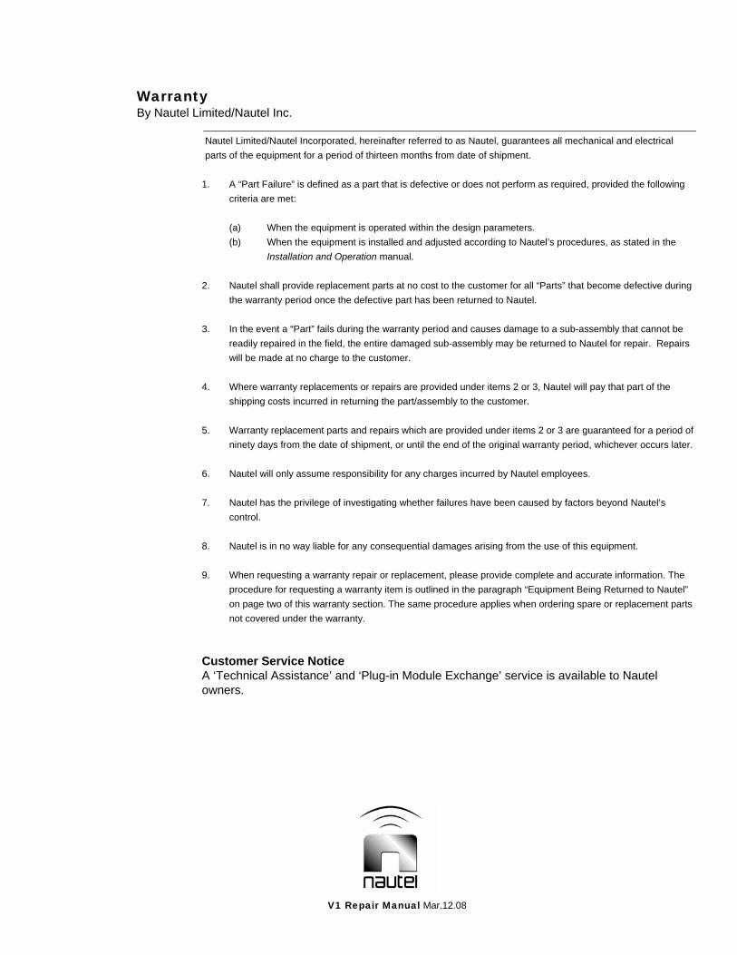
Warranty By Nautel Limited/Nautel Inc.
Nautel Limited/Nautel Incorporated, hereinafter referred to as Nautel, guarantees all mechanical and electrical parts of the equipment for a period of thirteen months from date of shipment.
1. A “Part Failure” is defined as a part that is defective or does not perform as required, provided the following criteria are met:
(a) When the equipment is operated within the design parameters. (b) When the equipment is installed and adjusted according to Nautel’s procedures, as stated in the
Installation and Operation manual.
2. Nautel shall provide replacement parts at no cost to the customer for all “Parts” that become defective during the warranty period once the defective part has been returned to Nautel.
3. In the event a “Part” fails during the warranty period and causes damage to a sub-assembly that cannot be
readily repaired in the field, the entire damaged sub-assembly may be returned to Nautel for repair. Repairs will be made at no charge to the customer.
4. Where warranty replacements or repairs are provided under items 2 or 3, Nautel will pay that part of the
shipping costs incurred in returning the part/assembly to the customer. 5. Warranty replacement parts and repairs which are provided under items 2 or 3 are guaranteed for a period of
ninety days from the date of shipment, or until the end of the original warranty period, whichever occurs later. 6. Nautel will only assume responsibility for any charges incurred by Nautel employees. 7. Nautel has the privilege of investigating whether failures have been caused by factors beyond Nautel’s
control. 8. Nautel is in no way liable for any consequential damages arising from the use of this equipment. 9. When requesting a warranty repair or replacement, please provide complete and accurate information. The
procedure for requesting a warranty item is outlined in the paragraph “Equipment Being Returned to Nautel” on page two of this warranty section. The same procedure applies when ordering spare or replacement parts not covered under the warranty.
Customer Service Notice A ‘Technical Assistance’ and ‘Plug-in Module Exchange’ service is available to Nautel owners.

V1 Repair Manual Mar.12.08
Factory Support TECHNICAL ASSISTANCE Nautel's field service department provides telephone technical assistance on a 24 hour, seven days a week basis. Requests by other media (facsimile or e-mail) will be responded to the next working day if received after Nautel's normal working hours. Contact the appropriate field service centre from the following: U.S.A. customers use: Nautel Incorporated T. +1.207.947.8200 (24 hours) or 877 6 nautel (628835) 201 Target Industrial Circle F. +1.207.947.3693 Bangor, Maine 04401 All other customers use: Nautel Limited T. +1.902.823.3900 (24 hours) or 877 6 nautel (628835) 10089 Peggy’s Cove Road, F. +1.902.823.3183 Hackett’s Cove, NS, Canada E-Mail [email protected] B3Z 3J4 Web www.nautel.com MODULE REPAIR SERVICE During the transmitter’s warranty period, repair of modules is performed at no charge to the customer. Once the warranty period has expired, module repairs will be invoiced based on material and labour costs. MODULE EXCHANGE SERVICE (North American Customers Only) North American customers can take advantage of Nautel’s module exchange service. This service gives customers a fast and efficient solution in the event of a hardware problem. When a customer’s transmitter experiences a failure, Nautel can send out a factory rebuilt module to replace the faulty module. Nautel’s two locations, Canada and the United States, provide quick turn around times, keeping our customers on the air. During the transmitter’s warranty period, exchange of modules is performed at no charge to the customer. Once the warranty has expired, the cost of a module exchange is only 40% of the list price for the module, provided the faulty module is returned to Nautel within 30 days and can be rebuilt; should the module not be returned an additional invoice for 40% of the list price will be issued. MODULE RETURN INSTRUCTIONS All equipment being returned to Nautel for repair or replacement should be marked with a Nautel provided RMA number and addressed to the appropriate Nautel facility. Complete and accurate information regarding the equipment will expedite shipment of replacement(s). Refer to the name plate on the transmitter and the appropriate module assembly and include with the shipment:
• Transmitter model number • Transmitter serial number • Module name
• Module serial number • Return shipping address
RETURN FACILITIES U.S.A. customers: RMA # Nautel Inc. Telephone: (207) 947-8200 x 109 201 Target Industrial Circle Fax: (207) 947-3693 Bangor, Maine 04401 USA Canadian. customers: RMA # Nautel Limited. Telephone: (902) 823-3900 x 100 Attention: Field Return Fax: (902) 823-3183 10089 Peggy’s Cove Road Hackett's Cove, NS B3Z 3J4 Canada

V1 Repair Manual Mar.12.08
Safety Symbols General definitions of safety symbols used on equipment or in manuals.
DANGER – HIGH VOLTAGE
Indicates dangerous voltages (in excess of 72 volts), capable of causing a fatal electrical shock, are present on or near parts bearing this label.
GROUND (EARTH)
Used with wiring terminals to indicate the terminal must be connected to earth ground before operating equipment. If power is supplied without grounding the equipment, there is a risk of receiving a severe or fatal electrical shock. Also used on electrical schematics to indicate a part that is connected to earth ground.
GROUND (PROTECTIVE or SAFETY)
Used with protective (safety) conductor terminals to indicate the terminal must be connected to ground before operating the equipment. If power is supplied without grounding the equipment, there is a risk of receiving a severe or fatal electrical shock.
ELECTROSTATIC SENSITIVE Indicates a part or assembly is or contains devices that are electrostatic sensitive. To prevent damage to these devices, ensure the handling procedures outlined in this manual are observed.
WARNING A WARNING denotes a hazard. It identifies an operating procedure,
condition, etc. which, if not strictly observed or adhered to, could result in injury or death to personnel. Throughout the technical manual, a WARNING shall immediately precede the text to which it applies.
CAUTION A CAUTION denotes a hazard. It identifies an operating procedure,
condition, etc., which, if not strictly observed or adhered to, could result in damage to, or destruction of the equipment. Throughout the technical manual, a CAUTION shall immediately precede the text to which it applies.
NOTE A NOTE denotes important information pertaining to an operating procedure,
condition, statement, etc., which is essential to highlight. A NOTE may precede or follow the text to which it applies.
V1 Repair Manual Mar.12.08
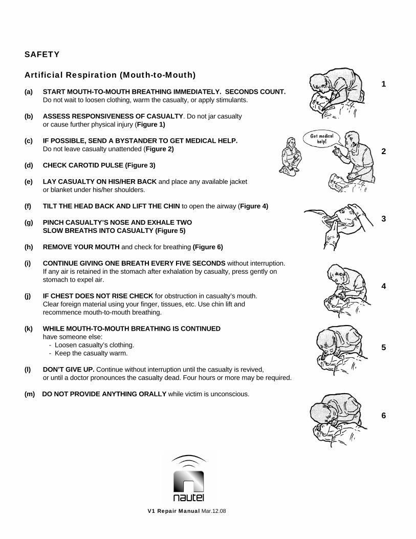
SAFETY Artificial Respiration (Mouth-to-Mouth) (a) START MOUTH-TO-MOUTH BREATHING IMMEDIATELY. SECONDS COUNT. Do not wait to loosen clothing, warm the casualty, or apply stimulants. (b) ASSESS RESPONSIVENESS OF CASUALTY. Do not jar casualty or cause further physical injury (Figure 1) (c) IF POSSIBLE, SEND A BYSTANDER TO GET MEDICAL HELP. Do not leave casualty unattended (Figure 2) (d) CHECK CAROTID PULSE (Figure 3) (e) LAY CASUALTY ON HIS/HER BACK and place any available jacket or blanket under his/her shoulders. (f) TILT THE HEAD BACK AND LIFT THE CHIN to open the airway (Figure 4) (g) PINCH CASUALTY’S NOSE AND EXHALE TWO SLOW BREATHS INTO CASUALTY (Figure 5) (h) REMOVE YOUR MOUTH and check for breathing (Figure 6) (i) CONTINUE GIVING ONE BREATH EVERY FIVE SECONDS without interruption. If any air is retained in the stomach after exhalation by casualty, press gently on stomach to expel air. (j) IF CHEST DOES NOT RISE CHECK for obstruction in casualty’s mouth. Clear foreign material using your finger, tissues, etc. Use chin lift and recommence mouth-to-mouth breathing. (k) WHILE MOUTH-TO-MOUTH BREATHING IS CONTINUED have someone else:
- Loosen casualty’s clothing. - Keep the casualty warm.
(l) DON’T GIVE UP. Continue without interruption until the casualty is revived, or until a doctor pronounces the casualty dead. Four hours or more may be required. (m) DO NOT PROVIDE ANYTHING ORALLY while victim is unconscious.
5
3
1
2
4
6

V1 Repair Manual Mar.12.08
SAFETY General Rules for Treatment for Burns, Bleeding, and Shock 1. After casualty has revived, treat for injuries and shock. 2. Reassure casualty. 3. Try to make him comfortable. 4. Keep him reasonably warm but do not apply heat. 5. If thirsty, liquids may be given but no alcohol (no liquids should be given in cases of severe burns). 6. Treat burns or wounds. Infection danger in treating burns or wounds is very great so ensure hands are
clean and do not handle affected areas more than necessary. 7. Do not apply salves, grease, etc. to burns. 8. Do not remove burned clothing that adheres to the skin or breaks blisters. 9. Cover the burn with a dry sterile dressing, piece of sheeting, etc. 10. Bandage lightly over blisters where care must be taken to cover and not to break. 11. If wound is bleeding severely, elevate affected area, except in the case of a fracture. 12. Expose wound and apply pressure. 13. Apply dressing, pad and bandage. 14. For burns and bleeding, immobilize injured part using splints if necessary and keep patient in restful
position during removal to hospital or expert medical attention. 15. In all cases, send for medical aid immediately.

V1 Repair Manual Mar.12.08
SAFETY Electric Shock - Rescue Methods Electricity can damage the body in a number of ways. It may interfere with the proper functioning of the nervous system and the heart action, subject the body to extreme heat and can cause severe muscular contractions. The path that the current of electricity takes through the body is important. Currents that pass from hand to hand or from hand to foot may pass directly through the heart and upset its normal functioning. This threat to life is related to the amount of current or amperage that will flow through a victim's body. Very little current (as little as 10 mA) can result in severe shock or death. Speed in the application of first aid measures is absolutely essential in cases of electrical injury. As soon as the victim is freed safely from the source of the electrical current, artificial respiration should be commenced immediately if breathing has stopped. If the carotid pulse cannot be felt, external cardiac massage should be commenced simultaneously. Resuscitation should continue until the patient is breathing on his own or until medical aid arrives. Survival rates can be quite high if cardiopulmonary resuscitation is started within 3 to 4 minutes of the injury being received. Act At Once - Delay or Indecision May Be Fatal 1. Turn OFF the electrical source. 2. Commence artificial respiration immediately. 3. Treat for burns, bleeding and shock. Removing a Casualty From Electrical Contact LOW VOLTAGE - 0 to 240 volts (household use) Switch off the current, if possible and time permits. If the switch cannot be located immediately and the supply is through a flexible cord or cable, the current may be shut off by removing the plug or even breaking the cable or wrenching it free. Never attempt to shut off current by cutting cord with a knife or scissors. If the current cannot be shut off, the greatest care is necessary in removing the casualty. Household rubber gloves, rubber or plastic hose (if there is no water in them), a dry unpainted stick or a clean dry rope can be used to free victim. HIGH VOLTAGE - 240 volts and up (industrial machines and power lines) Do not touch any person or equipment in contact with a wire. Use a dry unpainted pole, clean dry rope, dry rubber or plastic water hose to separate the casualty from the contact. Keep as far away as possible. Do not touch the casualty until the casualty is free.

V1 Repair Manual Mar.12.08
SAFETY Toxic Hazard Warning There are devices used in this equipment containing beryllium oxide ceramic, which is non-hazardous during normal device operation and under normal device failure conditions. These devices are specifically identified in the equipment parts list(s). DO NOT cut, crush or grind devices because the resulting dust may be HAZARDOUS IF INHALED. Unserviceable devices should be disposed of as harmful waste.


V1 Repair Manual Mar.12.08
Contents Page 1 GENERAL INFORMATION 1.1 PURPOSE AND SCOPE OF MANUAL 1-1 1.2 FAMILY TREE 1-1 1.3 GLOSSARY OF TERMS 1-1 2 THEORY OF OPERATION 2.1 INTRODUCTION 2-1 2.2 TRANSMITTER DESCRIPTION 2-1 2.3 AC-DC POWER STAGE 2-1 2.3.1 Ac Input 2-1 2.3.2 Switching Power Supply Module 2-2 2.3.3 LVPS Module 2-2 2.3.4 +12 V Fan Power Supply Module 2-2 2.3.5 Power Supply Interface PWB 2-2 2.4 RF STAGE 2-2 2.4.1 RF Drive Impedance Matching/Splitter Circuit 2-2 2.4.2 RF Drive Sample 2-2 2.4.3 Power Amplifiers 2-2 2.4.4 Reject Load PWB 2-3 2.4.5 Combiner Filtering 2-3 2.4.6 Power Probe PWB 2-3 2.5 CONTROL/MONITOR STAGE 2-4 2.5.1 Front Panel 2-4 2.5.1.1 Alarms Section 2-4 2.5.1.2 Diagnostic Display 2-4 2.5.1.3 Control Section 2-4 2.5.1.3.1 RF On/RF Off Selection 2-4 2.5.1.3.2 Power Increase/Decrease Selection 2-4 2.5.1.3.3 Local/Remote Status LEDs 2-4 2.5.2 Control/Interface PWB 2-5 2.5.2.1 Architecture 2-5 2.5.2.2 Alarm Monitoring 2-5 2.5.2.3 Analog Input Calibration 2-5 2.5.2.4 Microcontroller Interface 2-5 2.5.2.5 Software System 2-7 2.5.2.5.1 Read Status Task 2-7 2.5.2.5.2 RF Power Control Task 2-7 2.5.2.5.3 Update Display Task 2-7 2.5.2.5.4 Update Time Task 2-7 2.5.2.5.5 Internal Serial Update Task 2-7 2.5.2.5.6 Interrupt Tasks 2-7 2.5.2.6 Remote Interfacing 2-9 2.5.2.6.1 Remote Inputs 2-9

V1 Repair Manual Mar.12.08
Contents Page 2.5.2.6.2 Remote Outputs 2-9 2.5.2.6.3 Interlock Circuit 2-9 2.5.2.6.4 Exciter Link 2-9 2.5.2.6.5 Microcontroller 2-9 2.5.2.7 Power Amplifier Interface 2-9 2.5.2.7.1 PA Fail Detection 2-10 2.5.2.7.2 PA Bias Voltage 2-10 2.5.2.7.3 RF Drive Impedance Matching/Splitter 2-10 2.5.2.7.4 RF Drive Sample 2-10 2.5.3 NxLink Ethernet Interface Module (Optional) 2-10 2.6 COOLING FANS 2-10 3 COMPONENT LEVEL TROUBLESHOOTING 3.1 INTRODUCTION 3-1 3.2 ELECTROSTATIC DISCHARGE PROTECTION 3-1 3.2.1 Discharging of Personnel 3-1 3.2.2 Handling/Storage 3-1 3.2.3 Tools/Test Equipment 3-1 3.2.4 Stress Current Protection 3-1 3.3 COMPONENT REPLACEMENT PRECAUTIONS 3-2 3.4 SURFACE MOUNT TECHNOLOGY 3-2 3.4.1 Location of Parts 3-2 3.4.2 Soldering Guidelines 3-2 3.5 MAINTENANCE PROCEDURES 3-3 3.5.1 Power Amplifier PWB Maintenance 3-3 3.5.1.1 Tools and Reference Material Required 3-3 3.5.1.2 Visual Inspection 3-3 3.5.1.3 PA Input Checks 3-3 3.5.1.4 Power Amplifier PWB Replacement 3-4 3.5.2 Reject Load PWB Maintenance 3-5 3.5.2.1 Tools and Reference Material Required 3-5 3.5.2.2 Resistance Measurements 3-5 4 PARTS INFORMATION 4.1 INTRODUCTION 4-1 4.2 FAMILY TREE 4-1 4.3 HOW TO LOCATE INFORMATION FOR A SPECIFIC PART 4-1 4.3.1 When Nautel Configuration Control Number Is Known 4-1 4.3.2 When Ref Des Is Known 4-1

V1 Repair Manual Mar.12.08
Contents Page 4.4 REFERENCE DESIGNATION LISTS 4-1 4.5 COLUMN CONTENT 4-2 4.5.1 Ref Des Column 4-2 4.5.2 Description Column 4-2 4.5.3 Nautel # Column 4-2 4.5.4 Vendor # Column 4-2 4.5.5 OEM Code Column 4-2 4.6 OEM CODE TO MANUFACTURER CROSS-REFERENCE 4-2 4.6.1 Manufacturer’s Index 4-3 4.7 COMMON ABBREVIATIONS/ACRONYMS 4-3 5 WIRING INFORMATION 5.1 INTRODUCTION 5-1 5.2 WIRING LISTS NOT PROVIDED 5-1 5.3 PRINTED WIRING PATTERNS 5-1 5.4 WIRE COLOURS 5-1 5.5 WIRING LISTS PROVIDED 5-1 6 ELECTRICAL SCHEMATICS 6.1 INTRODUCTION 6-1 6.2 COMPONENT VALUES 6-1 6.3 GRAPHIC SYMBOLS 6-1 6.4 LOGIC SYMBOLS 6-1 6.5 REFERENCE DESIGNATIONS 6-1 6.6 UNIQUE SYMBOLOGY 6-1 6.6.1 Type of Inputs/Outputs 6-1 6.6.2 Logic Level/Convention 6-1 6.7 INDENTIFICATION OF SCHEMATIC DIAGRAMS 6-1 6.8 STRUCTURE OF SCHEMATICS 6-2 6.9 LOCATING THE SCHEMATIC DIAGRAM(S) FOR A FUNCTIONAL BLOCK 6-2 6-10 LOCATING A PART/ASSEMBLY INDENTIFIED ON A SCHEMATIC 6-2 7 MECHANICAL DRAWINGS 7.1 INTRODUCTION 7-1 7.2 LOCATING ASSEMBLY DETAIL DRAWINGS 7-1 7.3 CONTENT OF MECHANICAL DRAWINGS 7-1

V1 Repair Manual Mar.12.08
List of Tables Page
1-1 Glossary of Terms 1-2 2-1 RF Output Power Ratings 2-1 3-1 Maintenance Procedures 3-3 4-1 Manufacturer’s Index 4-3 5-1 Wiring Lists Provided 5-1 6-1 Electrical Schematics 6-3 7-1 Mechanical Drawings 7-2
List of Figures/Drawings Page
2-1 Block Diagram – Control/Display System 2-6 2-2 Flow Diagram – Control/Display Software System 2-8 2-3 Block Diagram – V1 FM Broadcast Transmitter 2-11 4-1 Family Tree – V1 FM Broadcast Transmitter 4-4

V1 Repair Manual Mar.12.08
Release Control Record Issue Date Reason
2.0 04 September 2007 Release 2 of equipment (NARF49/01)
2.1 16 October 2007 Updated NAPC153/01 schematics (SD-2 through SD-6) and assembly detail drawing (MD-3)
Changed 3.5.1.4 step (q) 2.2 12 March 2008 Updated schematics SD-1, SD-3, SD-4 and
SD-6 to accommodate changes for V2 combined systems


V1 Repair Manual Page 1-1 Section 1 General Information Issue 2.2
V1 REPAIR MANUAL Section 1 GENERAL INFORMATION
1.1 PURPOSE AND SCOPE OF MANUAL The Repair manual provides in-depth reference material to allow maintenance and troubleshooting beyond that provided in the Installation and Operation manual. This reference material includes: • Technical theory and functional block
diagrams of transmitter circuitry • Component level troubleshooting data to
aid in fault isolation • Parts lists for all assemblies and printed
wiring boards (PWBs) • Wiring lists and connector mating tables
for the transmitter’s cable harness • Electrical schematics for all assemblies
and PWBs
• Mechanical drawings of the transmitter, and most assemblies and PWBs
The information in this manual is intended for use by an experienced electronic technician. 1.2 FAMILY TREE The family tree for the V1 transmitter is depicted in Figure 4-1. It identifies the major assemblies and vendor items and shows the hierarchical assembly relationship. It also identifies the reference designation assigned to each assembly and vendor item. 1.3 GLOSSARY OF TERMS Table 1-1 provides a list of unique terms, abbreviations and acronyms used in this publication.

Page 1-2 V1 Repair Manual Issue 2.2 Section 1 General information
Table 1-1: Glossary of Terms TERM DESCRIPTION ADC Analog to Digital Converter
DAB Digital Audio Broadcast. Refers to any mode of digital operation.
DAC Digital to Analog Converter
GUI Graphic User Interface. Also referred to as diagnostic display
throughout this manual.
EEPROM
Electrically Erasable Programmable Read-Only Memory
IBOC In-Band On-Channel. An approach to deliver new digital services simultaneously with the existing analog broadcast.
LCD Liquid Crystal Display
LED Light Emitting Diode (also referred to as lamp)
Low Voltage Power Supply (LVPS)
Refers to a module within the transmitter which provides all of the necessary rail/supply voltages (excluding the power amplifier voltage).
LPF Low Pass Filter
PS Power Supply
PWB (PCB) Printed Wiring (Circuit) Board
RTC Real Time Clock
SRAM Static Random Access Memory
Switching Power Supply (SPS)
Refers to a module within the transmitter which supplies voltage to the RF power amplifiers.
UART Universal Asynchronous Receiver-Transmitter

V1 Repair Manual Page 2-1 Section 2 Theory of Operation Issue 2.2
V1 REPAIR MANUAL Section 2 THEORY OF OPERATION
2.1 INTRODUCTION The theory of operation for the V1 FM broadcast transmitter is presented in this section. Unique circuits are explained. Where applicable, the detailed theory for a module or assembly is provided in a separate paragraph in this section. A block diagram of the V1 transmitter is provided in Figure 2-3 at the end of this section. Electrical schematics SD-1 through SD-8 in Section 6 provide circuit details. 2.2 TRANSMITTER DESCRIPTION The V1 is broadband and can operate at any frequency between 87.5 MHz and 108 MHz. Table 2-1 indicates continuous RF power capabilities for all modes of operation. Table 2-1: RF Output Power Ratings Mode Power (W) Analog (FM) 1,400 (max.)
1,250 (rated) 30 (min.)
Hybrid (FM+HD) 1,000 (max.) 900 (rated) 130 (min.)
All-Digital (HD) 400 (max.) 360 (rated) 65 (min.)
The V1 may be operated locally where the V1 and studio are co-located or remotely where the V1 and studio are located at different sites. The V1 consists of three major stages: ac-dc power stage, RF stage and control/monitor stage.
2.3 AC-DC POWER STAGE See Figure SD-1. The ac-dc power stage converts the ac power source to a positive dc voltage (PA volts) for the V1’s RF power amplifiers. It also provides the V1’s regulated +24 V, ±15 V and +5 V supplies. The main components of the ac-dc power stage are the control/interface PWB A1, PS interface PWB A2, LVPS module U2, power supply module U3 and +12 V fan power supply U8. 2.3.1 Ac Input The ac input is applied to U1 on the back panel. Switch S1 controls the application of the ac voltage to the switching power supply module (U3, via PS interface PWB A2) and LVPS module U2. The V1 accepts an input between 180 and 264 V ac, 47 to 63 Hz. 2.3.2 Switching Power Supply Module See Figure SD-1. Switching power supply module U3 converts the ac input to the regulated PA volts supply for power amplifier (PA) PWBs A (A3) through D (A6). The module provides up to 2120 W output, at maximum levels of 53 V and 40 A. The module regulates the output voltage based on a PA Volts Control input from the control/monitor stage. A PA Volts Sample of the voltage is applied to a test point on PS interface PWB A2 for monitoring. The module has a built-in cooling fan and senses out-of-regulation and excessive temperature conditions and applies PS Fail and Supply Temp alarm signals to the control/monitor stage. Both conditions trigger an inhibit signal from the control/monitor stage to shut down the power supply, thus inhibiting the RF output.

Page 2-2 V1 Repair Manual Issue 2.2 Section 2 Theory of Operation
2.3.3 LVPS Module See Figure SD-1. LVPS module U2 converts the ac input voltage to the regulated low voltage dc supplies (+24 V, +15 V, +5 V and -15 V) applied to the control/monitor stage. 2.3.4 +12 V Fan Power Supply Module See Figure SD-1. Fan power supply module U3 converts the ac input voltage to the +12 V dc supply used by cooling fan B1. 2.3.5 Power Supply Interface PWB See Figure SD-1. Power supply (PS) interface PWB A2 provides an interface for all inputs (ac voltage, PA volts control, power supply inhibit) and outputs (PA volts, high temperature, power supply failure, ac failure) of switching power supply module U3. Test points are available to monitor the PA voltage, the power supply inhibit signal and the high temperature and power supply failure alarms. 2.4 RF STAGE See Figure SD-1. The RF stage accepts the RF input from an external RF drive source and generates the final RF output. It consists of RF drive splitting circuitry (part of control/interface PWB), four power amplifiers (A3 – A6), reject load PWB (A7), common point PWB (A8), a low-pass filter, power probe PWB (A9) and cooling fan B1. 2.4.1 RF Drive Impedance Matching/ Splitter Circuit See Figure SD-5. The control/interface PWB (A1) contains circuitry that accepts the external RF drive source and provides four equal RF drive signals for the RF power amplifiers. The external RF drive source (exciter) provides the RF In signal (J21). This signal is applied to an impedance matcher comprised of a 75 Ω Zo coaxial cable and coaxial cables T1:A and T1:B. These cables act to match the impedance between the RF In input and the splitter common point. Four equal signals are provided at connectors J17 through J20 to drive the PAs.
2.4.2 RF Drive Sample See Figure SD-5. The control/interface PWB (A1) contains circuitry that provides an RF drive sample voltage. A short section of micro-strip transmission line is in close proximity to the RF In input. Due to the proximity and orientation to the micro-strip, an RF voltage representative of the RF drive is induced in a power probe circuit. The RF drive signal is peak detected by A1CR4, A1R37, A1C60 and associated components. A dc voltage, proportional to the RF drive level, is applied to ADC A1U31 (pin 1) and to the RF DRV test point (TP12). The sample is used by monitoring and protection circuits. 2.4.3 Power Amplifiers See Figures SD-1 and SD-7. Each power amplifier PWB (A3 through A6) contains an identical, broadband, push-pull, RF power amplifier (PA). Each PA provides 375 W (nominal) of RF power in the FM band (87.5 to 108 MHz). The RF Drive, PA Volts and Bias inputs are provided by the control/ interface PWB (A1). Cooling air for the power amplifiers is provided by fan B1. The RF Drive input is applied to cable T1, which is connected as a balun to provide balanced, 180° out-of-phase, RF drive signals to the individual gates of dual N-channel power MOSFET (Q1). Cables T2:A and T2:B, as well as capacitors C2, C6 and C7, inductor L2 (part of R12/R13 leads) and resistors R5, R8. R9, R10, R12 and R13 provide impedance matching, which transforms the 50 Ω input to low impedance for application to Q1. The B+ (PA) voltage is applied to the individual drains of Q1 via inductors L4 and L5, which provide proper resonating reactance for Q1’s output. Cable T3:A and T3:B transform the impedance at the RF output, ensuring an optimum (low) impedance is presented at Q1’s output. Cable T4 converts the balanced RF signal to an unbalanced RF Output signal.

V3/5 Repair Manual Page 2-3 Section 2 Theory of Operation Issue 2.2
The PA voltage input is applied to capacitors C1, C3, C5, C8, C11 and C16, which act as a broadband decoupling network. Capacitor C13 and inductor L3 provide low-pass filtering of the RF signal back to the ac-dc power stage. The Bias input voltage is provided by the control/interface PWB to establish a dc bias current for Q1. The bias current depends on the operating mode. 2.4.4 Reject Load PWB See Figure SD-1. The reject load PWB (A7) provides a means to dissipate reject power between individual PAs. The four PA outputs are passed through the reject load PWB before being combined. Reject power generated by phase and amplitude imbalances between PAs is dissipated in power resistors R1 through R4. Thermistor RT1 monitors the temperature of the reject load PWB resistors and provides a Reject Load Temp signal to the control/interface PWB for thermal protection. 2.4.5 Combining/Filtering See Figure SD-1. The common point PWB (A8) combines the RF outputs from the four PAs to provide a single RF output. The low-pass filter attenuates harmonics and provides impedance matching between the common point (12.5 Ω) and the RF output (50 Ω).
2.4.6 Power Probe PWB See Figures SD-1 and SD-8. The power probe PWB (A9) monitors the V1’s forward and reflected power and generates the Fwd Pwr Sample (A9-A) and Refld Pwr Sample (A9-C) signals applied to the control/ interface PWB for protection and monitoring. The output from the low-pass filter is connected to the final RF Output (A9-G) by a micro-strip transmission line. Due to the probe’s proximity and orientation to this line, RF voltages representative of transmitter forward and reflected power are induced in respective probe circuits. The forward power output is peak-detected by A9CR1 and A9C6 and applied to A9-A. The reflected power output is peak-detected by A9CR2 and A9C5 and applied to A9-C. An RF monitor probe provides the RF Monitor output (A9-F), which is a nominal 1.1 V rms (FM mode at 1,250 W), 0.9 V rms (FM+HD mode at 900 W) or 0.6 V rms (HD mode at 360 W), for use with a modulation monitor or spectrum analyzer. An RF sample probe provides a similar (lower level) sample at A9-E. This sample – for M50 exciters only – is applied to the external exciter for use by the exciters’ adaptive pre-correction circuitry [for hybrid (FM+HD) or all-digital (HD) modes of operation only].

Page 2-4 V1 Repair Manual Issue 2.2 Section 2 Theory of Operation
2.5 CONTROL/MONITOR STAGE See Figures SD-1 through SD-6. The control/monitor stage, comprised primarily of the control/interface PWB (A1), performs the following functions: - provides local V1 controls, including a
diagnostic display that also indicates critical levels and alarm events
- contains monitoring and protection
circuits to prevent V1 damage under adverse or fault conditions
- monitors and distributes the RF drive
and the dc supply current to the power amplifiers
- provides remote interfacing for the V1 2.5.1 Front Panel See Figure SD-1. The front panel is the V1’s primary local interface. It contains the local transmitter controls, diagnostic display (GUI) and soft keys, and alarm indicating LEDs. Control and indicators are grouped into three sections of the panel – alarms section, diagnostic display, and control section. See Section 3 of the Installation and Operation Manual for detailed descriptions of each section. 2.5.1.1 ALARMS SECTION The alarms group is divided into four sections. Each section [Output Network (LED 1), PA (LED 2), Power Supply (LED 3) and External (LED 4)] contains an alarm lamp, which turns on when a fault occurs in that section.
2.5.1.2 DIAGNOSTIC DISPLAY The diagnostic display is a graphic user interface (GUI) that is navigated using five soft-keys. The majority of the transmitter’s local control (power presets, local/remote control, etc.) and monitoring (critical parameter levels, alarm events, etc.) may be performed from menus on this display. 2.5.1.3 CONTROL SECTION The control switches determine the V1’s RF status (on or off) and allow for power trim (increase and decrease). The RF on and off switches have integral LEDs that indicate the active selection. 2.5.1.3.1 RF On/RF Off Selection When the RF On button is pressed (enabled in Local mode only), the V1’s RF stage is enabled to provide an RF output. When the RF Off button is pressed, the V1’s RF stage and power supply module are inhibited. 2.5.1.3.2 Power Increase/Decrease Selection When the Power Increase button is pressed (enabled in Local mode only), the V1 enters the Preset menu, where further increase selections will cause the V1’s RF output to increase. When the Power Decrease button is pressed (enabled in Local mode only), the V1 enters the Preset menu, where further decrease selections will cause the V1’s RF output to decrease. Holding either button increases the rate of change of the power set point. 2.5.1.3.3 Local/Remote Status LEDs The Local and Remote LEDs indicate if the transmitter is being controlled locally (via its front panel) or remotely. Local and remote control selection is set up using the GUI.

V1 Repair Manual Page 2-5 Section 2 Theory of Operation Issue 2.2
2.5.2 Control/Interface PWB See Figures SD-2 through SD-6. The control/interface PWB (A1) contains the software systems for transmitter control/ display and remote monitoring. Its microcontroller (CPU) contains 128 KB of FLASH (program) memory, 4 KB of EEPROM and 4 KB of SRAM. There is also an external 32 KB of SRAM. 2.5.2.1 ARCHITECTURE The architecture of the control/display system (see Figure 2-1) is typical for this type of application. The CPU is supported with external memory, analog inputs and outputs, digital input and outputs and a user interface. The SRAM is primarily used to maintain a comprehensive events log. The user interface consists of an LCD display, front panel switches and LEDs. In addition to keeping time, the real time clock (RTC) block has other functions. It interfaces with a coin cell battery and system 5 V to maintain both itself and the SRAM in the event of ac loss to the transmitter. The RTC block also contains a watchdog timer which is essentially a software failure detection and recovery system. When the software is functioning properly, it ‘kicks’ the watchdog timer, resetting it. If the kicking stops, the watchdog timer will eventually overflow causing a hardware reset to the microcontroller and restarting the software.
2.5.2.2 ALARM MONITORING The unique characteristic of the control/ display system is the hardware support for alarm monitoring. ADCs read the level of analog inputs. Comparators generate hardware alarms from the analog inputs (low forward power, high reflected power, etc.) with programmable thresholds set through DACs. The comparator outputs are applied to a CPLD (complex programmable logic device) which generates an alarm interrupt to the microcontroller and forces a shutback of the RF output. The RF output recovers when the alarm condition is removed. 2.5.2.3 ANALOG INPUT CALIBRATION Calibration of analog inputs through the GUI ensures that the displayed metered value is accurate and also ensures that thresholds used for alarm reporting are correct. In the case of analog inputs with hardware comparators, the comparator threshold is an analog signal from a DAC that is adjusted according to the calibration. Other, non-critical, analog inputs are checked in software after being adjusted against the calibration value. 2.5.2.4 MICROCONTROLLER INTERFACE The microcontroller uses two serial buses. The SPI bus communicates with local devices such as the RTC, ADCs and DACs. An external serial bus, also UART based, connects to external equipment.

Page 2-6 V1 Repair Manual Issue 2.2 Section 2 Theory of Operation
Figure 2-1: Block Diagram – Control/Display System
SPI BUS
FWDPWR
REFLDPWR
PAFWD
BUS
H/WALARM
CPLD
PWR
AND
VOLTSEXCTR
RTC
VCC
SRAM
DATA
ADDRESS
SWITCH INTERRUPT
TEMPERATURE
FANVOLTSINTAKE,
REJ LD,
DIGITAL I/O
B2040504 VB
BATTERY
32K
WATCHDOG
ALARM INTERRUPT
EXHAUST
USERINTERFACE
LOGICSUPPLY
DIGITAL
RESET
SERIAL BUSEXTERNAL
SERIAL BUSRS-485 INTERNAL
VOLTS
ADCs, DACs AND COMPARATORS
OUTPUTS
MICROCONTROLLER

V1 Repair Manual Page 2-7 Section 2 Theory of Operation Issue 2.2
2.5.2.5 SOFTWARE SYSTEM See Figures 2-2 (a) and (b). The software in the control/display system has three essential functions. The flow diagram in Figure 2-2(a) illustrates the foreground tasks which run continuously at regular intervals. The flow diagram in Figure 2-2(b) illustrates the background or interrupt-driven tasks which run only when an input requires immediate servicing. 2.5.2.5.1 Read Status Task The read status task runs every 200 ms. It reads all of the system status and updates variables for other tasks. It also checks for ‘soft’ alarms which are non-critical in terms of timing but will force an event log to be created and may require an RF shutback. 2.5.2.5.2 RF Power Control Task The RF power control task runs whenever the RF is on and the transmitter is not being inhibited by an alarm. It handles a variety of tasks such as: • RF ramp up and shutback • foldback recovery • automatic level control (ALC) of the PA
voltage (FM mode) • power level control (FM+HD, HD mode) • monitor reflected power and forward
power The ALC function compares the actual RF power to the desired RF power. If the actual power is too high or low, the ALC adjusts the PA voltage to adjust the actual RF power. Shutback is the act of turning off the RF output due to an alarm. The foldback function checks for the alarm condition to clear and then attempts to recover the RF
output to its desired level. When shutback occurs due to high reflected power, a shutback will immediately clear the alarm because of the lack of RF output. As the RF power is restored, the reflected power may also increase. If so, the shutback function will only increase the RF output to a safe level. This is referred to as a foldback condition. The shutback function will continue running until RF power is fully restored. 2.5.2.5.3 Update Display Task The update display task runs every 250 ms. It updates the content on the GUI display. The status bar at the top line of the display is always updated. The middle six lines of the display are updated if they contain active parameters such as meter readings. 2.5.2.5.4 Update Time Task The update time task runs every 500 ms. It communicates with the RTC over the SPI bus to get the current time. 2.5.2.5.5 Internal Serial Update Task The internal serial update task consists of three functions which initiate regular communications with the microcontroller on the exciter to exchange status information. 2.5.2.5.6 Interrupt Tasks The interrupt tasks are used to handle time critical alarms and user initiated soft-key pressings on the front panel. The H/W alarm interrupt sets the shutback flag as a message to the RF power control task to start shutback recovery and calls the read status task to get a snapshot of the system status. The read status task calls the event log function which stores an alarm log.

Page 2-8 V1 Repair Manual Issue 2.2 Section 2 Theory of Operation
Figure 2-2: Flow Diagram – Control/Display Software System
EVENT
Y
N
SET
N
LOG
ALARM
Y
READ
KEY
UI
STATUS
CONTROL
MUTED
(b)
DISPLAY
SETUP
RESET
HANDLER
KEYS
READ
TIME EXCITER
B1980401 V1
WAIT 200ms
RF POWER
WAIT 250ms
(a)
UPDATE
WAIT 250ms
CALL
INTERRUPT
UPDATE
WAIT 500ms WAIT 1s
SERVICE
STATUS
FLAG
CONTROL SOFTWARE
SHUTBACK
READCALL
FRONT PANEL
H/W ALARMINTERRUPT

V1 Repair Manual Page 2-9 Section 2 Theory of Operation Issue 2.2
2.5.2.6 REMOTE INTERFACING The control/interface PWB has several functions related to external serial bus configuration and remote inputs and outputs. It contains customer interface connectors for transmitter remote control and remote alarm/ status monitoring. The following paragraphs provide brief descriptions of these functions. 2.5.2.6.1 Remote Inputs Remote control inputs are provided at back panel REMOTE I/O D-sub connectors (A1J3A and A1J3B) for remote control of the RF status, output power adjustment and selection of presets. These controls are enabled only after remote control has been selected through the GUI’s Control menu. They are operated by applying either a nominal +15 V between the (+) and (-) inputs or a ground to the (-) input (determined by input jumper configuration) of the desired control function. Refer to Section 2 of the Installation and Operation Manual for details on all remote inputs. 2.5.2.6.2 Remote Outputs Remote alarm, status and monitoring outputs are provided on back panel REMOTE I/O D-sub connectors (A1J3A and A1J3B). Alarm and status outputs are presented as logic level signals and are typically active ‘low’ (0 V). Analog voltage samples are provided to monitor critical transmitter parameters (forward and reflected power, PA voltage, etc). Refer to Section 2 of the Installation and Operation Manual for details on all remote outputs. 2.5.2.6.3 Interlock Circuit The XMTR INTLK inputs (pins 1 and 2 of back panel connector A1J4) must present a short circuit to ground when the interlock is intact and the RF output is safe to be enabled, and an open circuit when the RF output is to be inhibited.
2.5.2.6.4 Exciter Link The back panel EXCTR LINK RJ45 connector (A1J1) carries both the internal and external serial bus to allow communication with the digital exciter (for use with Nautel M50 only). 2.5.2.6.5 Microcontroller The microcontroller (U34) performs two roles: • It polls the digital inputs and assembles
their state into a response packet for the control/display software.
• It transfers digital output status information from packets received from the control/display software to the digital outputs.
The microcontroller does not manipulate or act on digital inputs or outputs other than to exchange state information with the control/display software. Digital inputs are polled every 100 ms, therefore a remote input must have a duration of at least 100 ms in order for it to be recognized. Similarly, digital outputs are refreshed every 100 ms. 2.5.2.7 POWER AMPLIFIER INTERFACE The control/interface PWB performs several functions to control and monitor the RF stage: - Monitors the current supplied to each PA
and causes an alarm condition if a PA stops drawing current.
- Splits the RF drive input to each PA and
provides a low level dc signal, proportional to the RF drive power, for monitoring and protection.
- Provides each PA’s dc bias voltage. - Inhibits the switching power supply
module when the appropriate fault occurs.

Page 2-10 V1 Repair Manual Issue 2.2 Section 2 Theory of Operation
2.5.2.7.1 PA Fail Detection See Figure SD-5. The voltages across resistors R159, R162, R166 and R168, representative of the individual PA currents, are applied to differential amplifiers U32, U36, U38 and U42. Their output voltages are applied to inputs of ADC U30. CUR1 (TP20) through CUR4 (TP17) test points are provided for monitoring. ADC U30’s output is fed to microcontroller U34. Microcontroller U34 outputs data to 8-bit shift register U8. During normal operation, when a PA is drawing current, the logic ‘low’ output of U8-1 is inverted at darlington IC U6:G output (open collector) to set the PA Fail Alarm output (J3A-2) to its non-alarm state (open collector). If no current is flowing through a PA, U8-1 will switch to logic ‘high’. This turns on darlington IC U6:G’s output and switches the PA Fail Alarm output to its alarm state (current-sink-to-ground). 2.5.2.7.2 PA Bias Voltage Microcontroller U34’s memory contains PA bias voltage settings for analog (FM), hybrid (FM+HD) and all-digital (HD) modes of V1 operation. The bias voltage information is loaded into 8-bit DAC U16. The corresponding analog outputs of U16 are applied through operational amplifiers (U14:A through U14:D) to the Bias 1 (J16-1) through Bias 4 (J16-4) outputs for application to the power amplifier PWBs. If microcontroller U34 causes a PA1 Inhibit through PA4 Inhibit signal (from latches U35:B through U35:E) to become active (logic low), NAND gate(s) U15:A through U15:D will switch to logic high and operational amplifiers U14:A through U14:D will apply a negative bias voltage to the power amplifier PWBs. A PA failure condition will also cause a negative bias voltage to be applied to the associated power amplifier PWB.
2.5.2.7.3 RF Drive Impedance Matching/ Splitter See description in 2.4.1. 2.5.2.7.4 RF Drive Sample See description in 2.4.2. 2.5.3 NxLink Ethernet Interface Module (Optional) See Figure SD-1 or the NxLink manual. An optional NxLink Ethernet interface module (U6) converts the internal serial protocol to Ethernet for external interfacing. When U6 is used, internal transmitter wiring supplies the module’s +15 V power supply, as well as the interfacing to the control/interface PWB and the external LAN (via RJ45 coupler U7). 2.6 COOLING FANS There are two cooling fans in the V1. One fan (B1) is located on the right-hand side, near the front. It is a dual fan that provides cooling air through the RF stage and exhausts air through ventilation holes in the back of the V1. B1 has two tachometer output signals to allow for speed monitoring on each side of the dual fan. Typical fan speed is 6000 RPM. The second fan is part of switching power supply module U3. It provides cooling air for the switching power supply module and exhausts air through ventilation holes in the back of the V1.

Dimensions = mm (inches)
Block Diagram – V1 FM Broadcast Transmitter Issue 2.2 Not to Scale Figure 2-3 Page 2-11
LAN*
+12V
D
A
B
C
+5V, +/-15V, +24V
(OPTIONAL)
POWERSUPPLY
CONTROL/
LOW PASSFILTER
DIRECTIONALCOUPLER
(TO M50 EXCITER)
RF MONITOR
RF OUTPUT
1-PHASE LOW
FAN
CONTROL
MODULE
NxLink
INTERFACECOMBINER
180-264VACAC POWER SOURCE
DRIVE INPUT
POWERSUPPLY
POWER
(TO M50 EXCITER)
MONITORINGETHERNETINTERFACE
EXTERNAL
RF SAMPLES
RF STAGE
B2040505 VA
EXTERNAL RF
EXTERNAL REMOTE
AC-DC POWER STAGE
VOLTAGE
SUPPLY
RF DRIVE
PA & BIAS VOLTS
REMOTE
EXCITER LINK POWERAMPLIFIERS
CONTROL/MONITOR STAGE
EXCITER RF SAMPLE
(FWD, REFLD)


V1 Repair Manual Page 3-1 Section 3 Component Level Troubleshooting Issue 2.2
V1 REPAIR MANUAL Section 3 COMPONENT LEVEL TROUBLESHOOTING
3.1 INTRODUCTION This section is intended to assist an experienced electronic technician in fault diagnosis and isolation of a problem to the component level. It is assumed that system level troubleshooting as outlined in the Installation and Operation Manual has been performed and the problem has been isolated to a particular PWB or assembly. Paragraphs 3.2 through 3.4 provide general protection and precaution information that should be followed throughout any component level troubleshooting or maintenance. Paragraph 3.5 and its sub-paragraphs provide maintenance procedures for certain transmitter modules. The modules must be removed from the transmitter to perform these procedures. 3.2 ELECTROSTATIC DISCHARGE PROTECTION The V1’s PWBs/assemblies contain semiconductor devices that are susceptible to damage from electrostatic discharge (ESD). The following precautions should be taken when handling an assembly that contains these devices:
NOTE Electrostatic energy is produced when two insulating materials are rubbed together. A person wearing rubber-soled shoes, walking across a nylon carpet or a waxed floor can generate an extremely large electrostatic charge. This effect is magnified during periods of low humidity. This high voltage may damage semiconductor devices such as integrated circuits, field-effect transistors, thyristors and Schottky diodes unless adequate precautions are taken.
3.2.1 Discharging of Personnel Personnel must be electrically discharged by a suitable ground system (anti-static mats, grounding straps) when removing an assembly from the V1 and while handling the assembly for maintenance procedures. 3.2.2 Handling/Storage The assembly should be placed in an anti-static bag when it is not installed in the V1 or when it is not being subjected to maintenance procedures. Electronic components should be stored in anti-static materials. 3.2.3 Tools/Test Equipment Testing and maintenance equipment, including soldering and unsoldering tools, should be suitable for contact with static sensitive semiconductor devices. A 40-watt, temperature controlled soldering iron is recommended. 3.2.4 Stress Current Protection Precautions should be taken to ensure the static sensitive semiconductor devices are protected from unnecessary stress current. This is achieved by ensuring: • Current is not flowing when an electrical
connection is broken. • Voltages are not present on external
control/monitoring circuits when they are connected.

Page 3-2 V1 Repair Manual Issue 2.2 Section 3 Component Level Troubleshooting
3.3 COMPONENT REPLACEMENT PRECAUTIONS When replacing a part on an assembly or a PWB containing through-hole plating: • Use of excessive heat or excessive
mechanical force can damage the PWB. Multi-layer PWBs are more susceptible to damage than two-sided PWBs.
• DO NOT replace components while the
PWB/assembly is mounted in the V1. • When removing a defective component,
cut the body from the legs before unsoldering the component. This will reduce the heat stress to the PWB’s traces.
• Use a solder removal tool or solder wick
whenever possible to remove the solder from the component’s legs before removing the device.
• Pre-form the legs of a replacement
component to fit the PWB hole spacing. This also applies to ICs that mount in sockets.
• For mechanically fastened components,
such as power MOSFETs, secure the mechanical connection before soldering the legs to reduce the stress on the solder connection.
3.4 SURFACE MOUNT TECHNOLOGY Compared to through-hole component technology, surface mount technology (SMT) enables highly efficient use of board space; however component replacement is more difficult. It is not practical to place SMT components in the V1 spares kit because of their small size. If the repair site is not already equipped to handle surface-mount technology, the following guidelines will aid in component replacement:
3.4.1 Location of Parts SMT components are predominantly on control/interface PWB A1. 3.4.2 Soldering Guidelines The following guidelines may help you when soldering SMT components on a PWB: (a) Recommended soldering aids: • needle tip for soldering iron • SMT solder (low melting point, fine
diameter) • water-soluble, ‘no-clean’ solder flux pen • magnifying glass • steady hand
(b) Clean pads using a solder braid. (c) Apply a thin layer of solder flux on the
pads. (d) For ICs, place the IC on the pads,
noting alignment, and gently press it in place. The flux should have enough adhesion to hold the chip in place.
(e) Carefully solder one corner pin, then
verify the IC's alignment. Solder the opposite corner pin, then verify alignment again.
(f) If alignment is correct, carefully solder
each pin, in order, around the IC. (g) If a solder bridge occurs, use a very fine
solder wick to remove it.

V1 Repair Manual Page 3-3 Section 3 Component Level Troubleshooting Issue 2.2
3.5 MAINTENANCE PROCEDURES Module maintenance determines if the subject module’s circuits are operating within defined parameters. The results determine if additional corrective action is required and in most cases will pin point faults to a specific circuit. Maintenance procedures should be performed after: • isolating a fault to the module level (see
Installation and Operation Manual) • removing the module from the V1 • putting the module on a suitable work
surface 3.5.1 Power Amplifier PWB Maintenance Maintenance on a power amplifier PWB consists of a visual inspection of the FET and associated solder connections, PA input checks and the likely replacement of the power amplifier PWB. Troubleshoot defective power amplifier PWBs as follows: 3.5.1.1 TOOLS AND REFERENCE MATERIAL REQUIRED • Digital multimeter • Torque-driver capable of torquing up to
6 inch-pounds (0.67 Newton-metres) • Electrical schematic SD-7 • Mechanical drawing MD-5 3.5.1.2 VISUAL INSPECTION Perform a visual inspection on the power amplifier PWB and its FET as follows: (a) Inspect the dual RF power FET of each
suspect power amplifier PWB for obvious signs of failure such as cracks in the case or overheating of the drain solder joints.
NOTE
Discoloration of the solder connection may indicate overheating of drain solder joints. If discoloration appears, the failure may have been caused by poor soldering.
(b) Check gate drive resistors R12 and R13 for discoloration. This may indicate a FET failure.
(c) Check the solder connection of the
coaxial cable connected to pad C on the power amplifier PWB for discoloration.
(d) Check resistors R3 and R4 and the 14
AWG wire in L1 for discoloration. This may result from PA oscillations.
(e) If there is damage, the entire power
amplifier PWB likely requires replacement. Check for additional possible causes of a failure (see 3.5.1.3) before replacing the power amplifier PWB (see 3.5.1.4).
NOTE
If it is found that the PA PWB is the source of the fault, you must replace the entire power amplifier PWB, rather than an individual FET. Two spare power amplifier PWBs are provided in the V1 spares kit, if purchased. To order a spares kit contact Nautel. Failure to observe this recommendation may void your equipment warranty or cause further failures. (f) If there is no obvious damage, perform
the PA input checks (see 3.5.1.3). 3.5.1.3 PA INPUT CHECKS Check the cabling between the control/ interface PWB’s RF drive splitter output and the suspect power amplifier's input as follows: (a) Disconnect the P1 end of the suspect
PA input coaxial cable(s) (W1 through W4) from the control/interface PWB output (A1J17 through A1J20). Disconnect the P2 end from J1 of the associated power amplifier PWB (A3 through A6).

Page 3-4 V1 Repair Manual Issue 2.2 Section 3 Component Level Troubleshooting
(b) Use a digital multimeter to measure continuity of the PA input cable(s) removed in step (a). The cable should measure short circuit (near 0 Ω) from core to core and from shield to shield. The cable should measure open circuit from core to shield (both ends). If a measurement does not comply, the PA input cable (W1 through W4) is defective.
(c) If no fault is found with the PA input
cable, replace the power amplifier PWB (see 3.5.1.4).
3.5.1.4 POWER AMPLIFIER PWB REPLACEMENT Replace a defective power amplifier PWB and, if necessary, configure the V1 for the replacement PWB as follows: (a) Ensure the coaxial cable (W1 through
W4) has been disconnected from J1 of the power amplifier PWB.
(b) Unsolder and remove the 16 AWG,
white wire (PA volts) from pad B of the power amplifier PWB.
(c) Unsolder and remove the 22 AWG,
white wire (bias) from pad A of the power amplifier PWB.
(d) Unsolder and remove the blue coaxial
cable (RF output) from pads C/D of the power amplifier PWB.
(e) Remove the two # 4 screws, split and
flat washers securing the FET to the heat sink.
(f) Remove the six nuts, split washers and
flat washers securing the power amplifier PWB to the chassis.
(g) Obtain the replacement power amplifier
PWB from the spares kit, if purchased. Retain the PA Bias Volts Data sheet provided with the replacement power amplifier PWB.
NOTE FETs are static sensitive and must be handled in a static protected manner. (h) Spread a small amount of thermal
compound (Nautel Part # HAG39, from the spares kit), thinly and evenly, on the bottom of the Q1 FET flange on the new power amplifier PWB.
(i) Install the power amplifier PWB on the
six studs on the chassis. Secure the power amplifier PWB to the chassis using the six sets of hardware removed in step (f). Ensure correct orientation (same as the adjacent PWB). Do not tighten the nuts at this time.
(j) Secure the FET (Q1) of the new power
amplifier PWB with two # 4 screws, a flat washer and a new split washer (user provided).
NOTE
You can damage the FET case if you fully tighten one screw while the other is loose. Try to alternate tightening of the two screws to prevent this. (k) Using a torque screwdriver, tighten the
screws to 6 inch pounds (0.672 Newton-meters).
(l) Tighten the six PWB nuts. (m) Solder and reconnect the wires removed
in steps (a) through (d). See Section 5, Wiring Information, to confirm wire positions.
(n) Reconnect the applicable coaxial cable
connector (W1-W4) to the appropriate power control/interface PWB (A1) connector.
CAUTION
Ensure the V1 is in an RF Off state until the PA bias setup is complete.
V1 Repair Manual Page 3-5 Section 3 Component Level Troubleshooting Issue 2.2
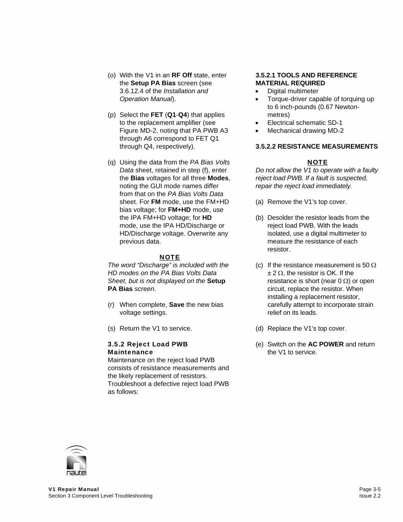
(o) With the V1 in an RF Off state, enter the Setup PA Bias screen (see 3.6.12.4 of the Installation and Operation Manual).
(p) Select the FET (Q1-Q4) that applies
to the replacement amplifier (see Figure MD-2, noting that PA PWB A3 through A6 correspond to FET Q1 through Q4, respectively).
(q) Using the data from the PA Bias Volts
Data sheet, retained in step (f), enter the Bias voltages for all three Modes, noting the GUI mode names differ from that on the PA Bias Volts Data sheet. For FM mode, use the FM+HD bias voltage; for FM+HD mode, use the IPA FM+HD voltage; for HD mode, use the IPA HD/Discharge or HD/Discharge voltage. Overwrite any previous data.
NOTE
The word “Discharge” is included with the HD modes on the PA Bias Volts Data Sheet, but is not displayed on the Setup PA Bias screen. (r) When complete, Save the new bias
voltage settings. (s) Return the V1 to service. 3.5.2 Reject Load PWB Maintenance Maintenance on the reject load PWB consists of resistance measurements and the likely replacement of resistors. Troubleshoot a defective reject load PWB as follows:
3.5.2.1 TOOLS AND REFERENCE MATERIAL REQUIRED • Digital multimeter • Torque-driver capable of torquing up
to 6 inch-pounds (0.67 Newton-metres)
• Electrical schematic SD-1 • Mechanical drawing MD-2 3.5.2.2 RESISTANCE MEASUREMENTS
NOTE Do not allow the V1 to operate with a faulty reject load PWB. If a fault is suspected, repair the reject load immediately. (a) Remove the V1’s top cover. (b) Desolder the resistor leads from the
reject load PWB. With the leads isolated, use a digital multimeter to measure the resistance of each resistor.
(c) If the resistance measurement is 50 Ω
± 2 Ω, the resistor is OK. If the resistance is short (near 0 Ω) or open circuit, replace the resistor. When installing a replacement resistor, carefully attempt to incorporate strain relief on its leads.
(d) Replace the V1’s top cover. (e) Switch on the AC POWER and return
the V1 to service.


V1 Repair Manual Page 4-1 Section 4 Parts Information Issue 2.2
V1 REPAIR MANUAL Section 4 PARTS INFORMATION
4.1 INTRODUCTION This section contains reference designation lists that provide descriptive and provisioning information for all electrical and mechanical parts that have an assigned reference designation and form a part of the subject equipment. 4.2 FAMILY TREE Figure 4-1 depicts the family tree for the subject equipment. It is based on the descending order of the reference designation hierarchy and identifies all assemblies that have an assigned Nautel configuration control number. 4.3 HOW TO LOCATE INFORMATION FOR A SPECIFIC PART To locate the information for a specific part, the assigned reference designation for the part must be known. In addition, the Nautel configuration control number (e.g., NAPC153/01) assigned to the assembly containing the part or the full reference designation, including the reference designation of all higher assemblies, must be known. 4.3.1 When Nautel Configuration Control Number Is Known When the Nautel configuration control number is known, the information for a part can be located as follows: • Refer to the family tree (Figure 4-1) and
identify the block(s) associated with the Nautel configuration control number. Unless otherwise specified, each family tree block has its own PART NUMBER INDEX TABLE. Locate the part's reference designation in the identified reference designation list in this section, noting they are sorted alphanumerically.
4.3.2 When Ref Des Is Known When the full reference designation is known, the information for a part can be located as follows: • Refer to the family tree depicted in Figure
4-1 with the full reference designation. • Follow the family tree branches to the
block that represents the lowest level assembly assigned a Nautel configuration control number. Then locate the part number index table for that Nautel configuration control number.
• Locate the part's reference designation in
the specified table. 4.4 REFERENCE DESIGNATION LISTS Individual reference designation lists are provided for: • assemblies that are assigned an alpha-
prefixed Nautel nomenclature (e.g., NAPC153/01)
• cable sets that are assigned a numbered
Nautel part (e.g., 204-8402-01) • optional items that are assigned a
numbered Nautel part (e.g., 204-8443) To obtain the full reference designation for a specific part the Nautel configuration control number must be located in the family tree (Figure 4-1) to include the reference designation of all higher level assemblies. The reference designation lists, which are titled and presented in alphanumeric order, are divided into columns to aid in locating specific information.

Page 4-2 V1 Repair Manual Issue 2.2 Section 4 Parts Information
4.5 COLUMN CONTENT The following paragraphs provide an explanation of the purpose and contents of each column in the part number indexes. 4.5.1 Ref Des Column The ‘ref des’ column contains the reference designation for a specific part. These designations are assigned in accordance with the requirements of American National Standard Specification ANSI Y32.16. 4.5.2 Description Column This column contains the name and descriptive information for each part. The key word is presented first, followed by the adjective identifiers. When the description is 'See Family Tree for Assembly Nomenclature', the associated part is subject to its own part index table or is contained in an optional kit’s list. Look up the reference designation list title (nomenclature) and the reference designation of the associated part in the family tree (Figure 4-1) to determine where to locate its part information. 4.5.3 Nautel # Column This column contains the Nautel number assigned to each part. This number is Nautel's drawing number for Nautel manufactured parts, Nautel's configuration control number for assemblies that are under configuration control management, or Nautel's inventory management number for purchased parts. When a Nautel configuration control number (e.g. NAPC*) is referenced in this column, the associated ref des item is subject to its own part index table. 4.5.4 Vendor # Column This column contains an original equipment manufacturer's part number for a part. A single part number is listed for each part, even though there may be more than one known manufacturer. The listed number is Nautel's usual or preferred choice. The use of this number does not restrict Nautel from selecting and using commercial equivalents during manufacture, where their use will not degrade circuit operation or reliability.
4.5.5 OEM Code Column This column typically contains a five digit coded group as the original equipment manufacturer's (OEM) identifier. The code was extracted from Cataloging Handbook H4/H8 - Commercial and Government Entity (Cage) Code. Manufacturers that were not listed in the catalog when this listing was compiled have been assigned a unique five-letter code. This code is assigned arbitrarily and has no other significance. The manufacturers identified for parts that have JAN or MIL part numbers are Nautel's normal supply source for that part.
NOTE OEM code 37338 is listed for parts manufactured by Nautel or to a Nautel control drawing. United States of America customers should refer all replacement part orders to Nautel Incorporated (OEM code 57655). 4.6 OEM CODE TO MANUFACTURER CROSS-REFERENCE The OEM (CAGE) codes listed in the reference designation lists are representative of the original equipment manufacturers of those parts. To determine a specific part’s manufacturer contact information, enter the five-character OEM (CAGE) code for that part in the following website: https://www.bpn.gov/bincs/begin_search.asp After entering the OEM (CAGE) code number, manufacturer pertinent information (address, telephone number, fax number, etc.) will be displayed. Please contact Nautel if a part cannot be obtained (see also ON-LINE PART QUOTES in the Warranty section of this manual).

V1 Repair Manual Page 4-3 Section 4 Parts Information Issue 2.2
4.6.1 Manufacturer’s Index For customers without web access, Table 4-1 provides a cross-reference from the original equipment manufacturer’s (OEM) codes to the manufacturer’s name. The listing is sorted alphanumerically by the OEM code.
4.7 COMMON ABBREVIATIONS/ ACRONYMS The following abbreviations/acronyms may appear in the Description column: SMT - Denotes item is designed to be installed
using Surface Mount Technology. MTA - Denotes item is a Mass Termination
Assembly connector. SIP - Single In-line Package DIP - Dual In-line Package IDC - Denotes item is an Insulation
Displacement connector for ribbon cable.
Table 4-1: Manufacturer’s Index APP Anderson Power Products C3057 Conec Elektronische Bauelemente GMBH EDAC Edac Incorporated FERROX Ferroxcube Corp. Interpower Interpower Corporation IR International Rectifier NKK Switch NKK Switches of America PANAS See 0J4G8 PHOENIX Phoenix Contact Incorporated ST MICRO See U3040 SUPRE Supre International Limited TAIKO TAIKO Electronic TECTROL Tectrol Inc. TYCO Tyco Electronics U3040 ST Microelectronics Ltd. VENKEL Venkel Ltd. 0B0A9 Dallas Semiconductor Corporation 0GP12 Radiall Incorporated 0J4G8 Panasonic Industrial Co. 00779 CTS Company Incorporated 01295 Texas Instruments Incorporated 02660 Amphenol Corp Spectra-Strip/ITD 04713 Motorola Incorporated 06090 Raychem Corporation 07263 Fairchild Camera and Instrument Corp 09482 Amp of Canada Limited 1BH13 Fenwall Electronics Inc. 1E566 Alpha Photo Products Inc.
1FN41 Atmel Corporation 1JRT7 Epson Electronics American, Inc 1MQ07 ZRG Incorporated 14433 ITT Semiconductors Div. 14655 Cornell Dubilier Electronics 27014 National Semiconductor Corp 29990 American Technical Ceramics Corp. 3DX59 Citizen America Corporation 31433 Kemet Electronics Corporation 33062 Ferronics Incorporated 37338 Nautel Ltd. 45496 Digital Systems 50434 Hewlett Packard Company 56289 Sprague Electric Company 56845 Vishay Dale Electronics Incorporated 59124 KOA Speer Electronics Incorporated 64155 Linear Technology Corporation 65786 Cypress Semiconductor Corp. 68994 XILINX Incorporated 7D893 Fairchild Semiconductor Corporation 70903 Belden Wire and Cable Co. 74116 New England Wire Technologies Corp. 75042 TRW Incorporated 83330 Dialight Corporation, DBA Dialight 91833 Keystone Electronics Corporation 91929 Honeywell Incorporated 92194 Alpha Wire Corp.

Page 4-4 V1 Repair Manual Issue 2.2 Section 4 Parts Information
Figure 4-1: Family Tree – V1 FM Broadcast Transmitter
F2040506 V3
A2PS INTERFACE PWB
204-7650-01
POWER AMPLIFIER PWB 'D'A6
NAPA16A
POWER AMPLIFIER PWB 'B'A4
NAPA16A
(SEE PART NUMBER INDEX TABLES)
V11000 WATT FM BROADCAST TRANSMITTER
NARF49/01
A7REJECT LOAD PWB
PN85B
A8COMMON POINT PWB
PN95B
POWER AMPLIFIER PWB 'C'A5
NAPA16A
POWER AMPLIFIER PWB 'A'A3
NAPA16A
A1CONTROL/INTERFACE PWB
NAPC153/01
POWER PROBE PWBA9
204-8490-01

204-2045-01 Mod, UDDS01 LCD
REFDES NAUTEL #DESCRIPTION VENDOR # OEM CODE
RT01 RX07Thermistor, 200K Ohms @ 25C 135-204QAG-J01 1BH13
204-7650-01 PS Interface PWB Assy
REFDES NAUTEL #DESCRIPTION VENDOR # OEM CODE
E01 HR26Connector, Quick-Dis, M,1/4 Tab, PWB 1287 91833
E02 HR26Connector, Quick-Dis, M,1/4 Tab, PWB 1287 91833
J01 UJ01Conn,Socket,Pwr Drwr,w/10xSP20-GN 075MSF-A07 APP J02 JA49Conn, Header, Ribbon Cbl, 10 pin 499910-1 00779
Page 1 of 27 204-7650-01

204-8402-01 Cable Set Assy, V1 (RLS 2)
REFDES NAUTEL #DESCRIPTION VENDOR # OEM CODE
A02 204-7650-01PS Interface PWB Assy 204-7650-01 37338
J01 JT60Conn, Coax, BNC, Recept,Bulkhead, RG188 31-318 02660
J05 JR27Conn, Socket, D-Sub, 9 pin 205203-1 09482 P01 JU46MTA,Closed End Housing,3 pin,22 AWG 3-640433-3(ROHS) TYCO
P01 JU47MTA,Standard Dust Cover,3 pin 640551-3(ROHS) TYCO
P02 JU07MTA, Standard Dust Cover, 8 pin 640551-8 09482 P02 JU28MTA, Keyed Closed End Housing,8 pin,22AWG 644463-8 00779
P03 JU07MTA, Standard Dust Cover, 8 pin 640551-8 09482
P03 JU28MTA, Keyed Closed End Housing,8 pin,22AWG 644463-8 00779 P04 JP50Conn, Recept, Ribbon Cable, 10 pin 746285-1 00779
P05 JP50Conn, Recept, Ribbon Cable, 10 pin 746285-1 00779 P06 JDP24Conn, Coax, BNC, Plug, 50ohm,Crimp 225395-7 09482
P07 JT50Conn, Plug, 3-Pin, Mate-N-Lok 350766-1 00779
P08 JT50Conn, Plug, 3-Pin, Mate-N-Lok 350766-1 00779 P09 JU02MTA, Standard Dust Cover, 4 pin 640551-4 09482
P09 JU27MTA, Keyed Closed End Housing,4 pin,22AWG 644463-4 00779
P10 JU07MTA, Standard Dust Cover, 8 pin 640551-8 09482 P10 JU28MTA, Keyed Closed End Housing,8 pin,22AWG 644463-8 00779
P11 HAM05Connector, Quick-Dis, F,1/4 Tab 2-520184-2 09482
P16 HAM05Connector, Quick-Dis, F,1/4 Tab 2-520184-2 09482 P17 JU40MTA, Standard Dust Cover,5-pin 640551-5 00779
P17 JU50MTA,Closed End Housing,5 pin,Str,22AWG 3-640433-5(ROHS) L2433
P18 JU54MTA, Closed End Housing, 6 pin22AWG 3-640433-6(RoHS) TYCO P18 JU55MTA, Standard Dust Cover, 6pin 640551-6(RoHS) TYCO
P19 JU02MTA, Standard Dust Cover, 4 pin 640551-4 09482 P19 JU27MTA, Keyed Closed End Housing,4 pin,22AWG 644463-4 00779
P20 HAM05Connector, Quick-Dis, F,1/4 Tab 2-520184-2 09482
204-8407-01 Fan Assy, V1 (Dual Blower)
REFDES NAUTEL #DESCRIPTION VENDOR # OEM CODE
L01 LA02Toroid, Ferrite, 12.7mm, K Mtl 11-262-K 33062
L02 LA02Toroid, Ferrite, 12.7mm, K Mtl 11-262-K 33062 P1 JU07MTA, Standard Dust Cover, 8 pin 640551-8 09482
P1 JU28MTA, Keyed Closed End Housing,8 pin,22AWG 644463-8 00779
Page 2 of 27 204-8407-01

204-8490-01 Power Probe PWB Assy
REFDES NAUTEL #DESCRIPTION VENDOR # OEM CODE
C01 -Not Used NOT USED 37338
C02 -Not Used NOT USED 37338
C03 -Not Used NOT USED 37338 C04 -Not Used NOT USED 37338
C05 CCG01Capacitor, Ceramic, 0.001uF 10% 200V CKR05BX102KRV SPRAGUE
91929
C06 CCG01Capacitor, Ceramic, 0.001uF 10% 200V CKR05BX102KRV SPRAGUE
91929
C07 -Not Used NOT USED 37338
C08 -Not Used NOT USED 37338 CR01 QK09Diode, Schottky 1N5711 (STATIC) 50434
CR02 QK09Diode, Schottky 1N5711 (STATIC) 50434 R01 RAB06Resistor, MF, 27.4 Ohms, 1PC 1/4W MF1/4DL27R4F 59124
R02 RAB06Resistor, MF, 27.4 Ohms, 1PC 1/4W MF1/4DL27R4F 59124
R03 RAB06Resistor, MF, 27.4 Ohms, 1PC 1/4W MF1/4DL27R4F 59124 R04 -Not Used NOT USED 37338
R05 RAB15Resistor, MF, 150 Ohms, 1PC 1/4W MF1/4DL1500F 59124
R06 RAB15Resistor, MF, 150 Ohms, 1PC 1/4W MF1/4DL1500F 59124 R07 RAB05Resistor, MF, 22.1 Ohms, 1PC 1/4W MF1/4DL22R1F 59124
R08 RAB08Resistor, MF, 39.2 Ohms, 1PC 1/4W MF1/4DL39R2F 59124
R09 RAB05Resistor, MF, 22.1 Ohms, 1PC 1/4W MF1/4DL22R1F 59124 R10 -Not Used NOT USED 37338
R11 RAB15Resistor, MF, 150 Ohms, 1PC 1/4W MF1/4DL1500F 59124
R12 RAB15Resistor, MF, 150 Ohms, 1PC 1/4W MF1/4DL1500F 59124 R13 RAB13Resistor, MF, 100 Ohms, 1PC 1/4W MF1/4DL1000F 59124
R14 RAB13Resistor, MF, 100 Ohms, 1PC 1/4W MF1/4DL1000F 59124 R15 RAB31Resistor, MF, 3.32K Ohms, 1PC1/4W MF1/4DL3321F 59124
R16 RAB31Resistor, MF, 3.32K Ohms, 1PC1/4W MF1/4DL3321F 59124
R17 RC27Resistor, Film, 150 Ohms, 2PC1/2W RL20S151G 35005 R18 RC27Resistor, Film, 150 Ohms, 2PC1/2W RL20S151G 35005
R19 -Not Used NOT USED 37338
Page 3 of 27 204-8490-01

NAPA16A PA PWB Assy, HD
REFDES NAUTEL #DESCRIPTION VENDOR # OEM CODE
C01 CT38Capacitor, Metal, Polyester, 10uF 100V DME1W10K 14655
C02 CT47Capacitor,SMT,Ceramic,15pF,50V,5% C1206C150J5GAC 91929
C03 CT38Capacitor, Metal, Polyester, 10uF 100V DME1W10K 14655 C04 -Not Used NOT USED 37338
C05 CAP16Capacitor, Ceramic, 1.0uF 100V RPE114Z5U105M100V
91929
C06 CT49Capacitor,SMT,Ceramic,100pF,50V,5% C1206C101J5GAC 91929
C07 CT48Capacitor,SMT,Ceramic,56pF,50V,5% C1206C560J5GAC 91929
C08 CAP16Capacitor, Ceramic, 1.0uF 100V RPE114Z5U105M100V
91929
C09 CT50Capacitor,SMT,Ceramic,0.01uF,100V,10% C1206C103K1RAC 91929
C10 CCG04Capacitor, Ceramic, 0.01uF 10% 100V CKR05BX103KRV 56289 C11 CT51Capacitor,SMT,Ceramic,0.1uF,100V,10% C1812C104K1RAC 91929
C12 CT50Capacitor,SMT,Ceramic,0.01uF,100V,10% C1206C103K1RAC 91929
C13 CT52Capacitor,SMT,Ceramic,470pF,200V,10% ATC100B471KW200X 29990 C14 CT53Capacitor,SMT,Ceramic,0.001uF,50V,10% ATC100B102KW50X 29990
C15 CT53Capacitor,SMT,Ceramic,0.001uF,50V,10% ATC100B102KW50X 29990
C16 CAP62Cap,Electrolytic,1000uF,+/-20%,75V,Radial lead 361R102M075FV2 14655 J01 JT43Conn, Coax, Recept, 20 Deg.Low Profile TMP-S01X-B1 TAIKO
L01 LA42Core, Ferrite, 2 hole, 4B1 mtl MHB2-14/8.5/14-4B1 FERROX
L01 WB05Wire, 16 AWG, Stranded, White H0102005 SUPRE L02 -Not Used NOT USED 37338
L03 WE47Wire,18AWG,Magnet,Anaclad-A,Red 8049 70903
L04 WF08Wire, 14 AWG, Tinned Copper 286 92194 L05 WF08Wire, 14 AWG, Tinned Copper 286 92194
L06 LA45Core, Ferrite, 2 Hole, K Mtl 12-365-K 33062 L07 LA45Core, Ferrite, 2 Hole, K Mtl 12-365-K 33062
Q01 QAP58Transistor, (BeO), FET, NChannel, Dual SD2942(STATIC) ST MICRO
R01 RAD39Resistor, SMT, MF, 15K Ohms,1%, 1/4W RK73H2BL1502F 59124 R03 RAD50Resistor,SMT,MF,20ohms,1%,2W CR2512-2W-20R0F VENKEL
R04 RAD50Resistor,SMT,MF,20ohms,1%,2W CR2512-2W-20R0F VENKEL
R05 RAD50Resistor,SMT,MF,20ohms,1%,2W CR2512-2W-20R0F VENKEL R06 -Not Used NOT USED 37338
R07 -Not Used NOT USED 37338
R08 RAD50Resistor,SMT,MF,20ohms,1%,2W CR2512-2W-20R0F VENKEL R09 RAD50Resistor,SMT,MF,20ohms,1%,2W CR2512-2W-20R0F VENKEL
R10 RAD50Resistor,SMT,MF,20ohms,1%,2W CR2512-2W-20R0F VENKEL
R11 RAD45Resistor, SMT, MF, 47.5K Ohms, 1% 1/4W RK73H2BL4752F 59124 R12 RBP01Resistor, Film, 10 Ohms, 5%, 2W GS-3, 10 OHMS 75042
R13 RBP01Resistor, Film, 10 Ohms, 5%, 2W GS-3, 10 OHMS 75042
Page 4 of 27 NAPA16A

Continued from previous page
NAPA16A PA PWB Assy, HD
REFDES NAUTEL #DESCRIPTION VENDOR # OEM CODE
T01 WE38Cable, Coax, 50ohm, Strand, RG188A/U A4188A 14433
T02A WF17Wire, 22 AWG, Stranded, 1-cond/shield,Tef 83305 70903
T02B WF17Wire, 22 AWG, Stranded, 1-cond/shield,Tef 83305 70903 T03A WF22Wire, 16 AWG, 1-Cond/Shield, Teflon 83308 70903
T03B WF22Wire, 16 AWG, 1-Cond/Shield, Teflon 83308 70903
T04 WE46Cable,Coax,50 ohm,82.5% VP,SRJacket,NEWcel-GX16 N32-32S-259-6 74116
Page 5 of 27 NAPA16A

NAPC153/01 Control/Interface PWB Assy,V1
REFDES NAUTEL #DESCRIPTION VENDOR # OEM CODE
BT01 BBLT01Battery, Lithium, 3V,20mm Coin Cell CR2032 PANAS
C001 CCFS07Cap,SMT,Ceramic,0.1uF,10%,50V,X7R,0805 C0805C104K5RAC 31433
C002 CCFS07Cap,SMT,Ceramic,0.1uF,10%,50V,X7R,0805 C0805C104K5RAC 31433 C003 CCFS07Cap,SMT,Ceramic,0.1uF,10%,50V,X7R,0805 C0805C104K5RAC 31433
C004 CCFS07Cap,SMT,Ceramic,0.1uF,10%,50V,X7R,0805 C0805C104K5RAC 31433
C005 CCFS07Cap,SMT,Ceramic,0.1uF,10%,50V,X7R,0805 C0805C104K5RAC 31433 C006 CCFS04Cap,SMT,Ceramic,0.01uF,10%,50V,X7R,0603 C0603C103K5RAC 31433
C007 CCFS04Cap,SMT,Ceramic,0.01uF,10%,50V,X7R,0603 C0603C103K5RAC 31433
C008 CCFS07Cap,SMT,Ceramic,0.1uF,10%,50V,X7R,0805 C0805C104K5RAC 31433 C009 CCFS07Cap,SMT,Ceramic,0.1uF,10%,50V,X7R,0805 C0805C104K5RAC 31433
C010 CCFS01Cap,SMT,Ceramic,0.001uF,10%,50V,X7R,0603 C0603C102K5RAC 31433 C011 CCFS01Cap,SMT,Ceramic,0.001uF,10%,50V,X7R,0603 C0603C102K5RAC 31433
C012 CCFS01Cap,SMT,Ceramic,0.001uF,10%,50V,X7R,0603 C0603C102K5RAC 31433
C013 CCFS01Cap,SMT,Ceramic,0.001uF,10%,50V,X7R,0603 C0603C102K5RAC 31433 C014 CCFS01Cap,SMT,Ceramic,0.001uF,10%,50V,X7R,0603 C0603C102K5RAC 31433
C015 CCFS10Cap,SMT,Ceramic,1uF,10%,25V,,X7R,1206 C1206C105K3RAC 31433
C016 CCFS04Cap,SMT,Ceramic,0.01uF,10%,50V,X7R,0603 C0603C103K5RAC 31433 C017 CCFS07Cap,SMT,Ceramic,0.1uF,10%,50V,X7R,0805 C0805C104K5RAC 31433
C018 CCFS01Cap,SMT,Ceramic,0.001uF,10%,50V,X7R,0603 C0603C102K5RAC 31433
C019 CCFS01Cap,SMT,Ceramic,0.001uF,10%,50V,X7R,0603 C0603C102K5RAC 31433 C020 CCFS01Cap,SMT,Ceramic,0.001uF,10%,50V,X7R,0603 C0603C102K5RAC 31433
C021 CCFS01Cap,SMT,Ceramic,0.001uF,10%,50V,X7R,0603 C0603C102K5RAC 31433
C022 CCFS01Cap,SMT,Ceramic,0.001uF,10%,50V,X7R,0603 C0603C102K5RAC 31433 C023 CTFS03Cap,SMT,Tantalum,10uF,10%,35V,2917 T494D106K035AS 31433
C024 CCFS01Cap,SMT,Ceramic,0.001uF,10%,50V,X7R,0603 C0603C102K5RAC 31433 C025 CCFS01Cap,SMT,Ceramic,0.001uF,10%,50V,X7R,0603 C0603C102K5RAC 31433
C026 CCFS01Cap,SMT,Ceramic,0.001uF,10%,50V,X7R,0603 C0603C102K5RAC 31433
C027 CCFS01Cap,SMT,Ceramic,0.001uF,10%,50V,X7R,0603 C0603C102K5RAC 31433 C028 CCFS01Cap,SMT,Ceramic,0.001uF,10%,50V,X7R,0603 C0603C102K5RAC 31433
C029 CCFS01Cap,SMT,Ceramic,0.001uF,10%,50V,X7R,0603 C0603C102K5RAC 31433
C030 CCFS01Cap,SMT,Ceramic,0.001uF,10%,50V,X7R,0603 C0603C102K5RAC 31433 C031 CCFS01Cap,SMT,Ceramic,0.001uF,10%,50V,X7R,0603 C0603C102K5RAC 31433
C032 CCFS04Cap,SMT,Ceramic,0.01uF,10%,50V,X7R,0603 C0603C103K5RAC 31433
C033 CCFS07Cap,SMT,Ceramic,0.1uF,10%,50V,X7R,0805 C0805C104K5RAC 31433 C034 CCFS07Cap,SMT,Ceramic,0.1uF,10%,50V,X7R,0805 C0805C104K5RAC 31433
C035 CCFS07Cap,SMT,Ceramic,0.1uF,10%,50V,X7R,0805 C0805C104K5RAC 31433
C036 CTFS03Cap,SMT,Tantalum,10uF,10%,35V,2917 T494D106K035AS 31433 C037 CCFS04Cap,SMT,Ceramic,0.01uF,10%,50V,X7R,0603 C0603C103K5RAC 31433
C038 CCFS04Cap,SMT,Ceramic,0.01uF,10%,50V,X7R,0603 C0603C103K5RAC 31433
Page 6 of 27 NAPC153/01

Continued from previous page
NAPC153/01 Control/Interface PWB Assy,V1
REFDES NAUTEL #DESCRIPTION VENDOR # OEM CODE
C039 CCFS07Cap,SMT,Ceramic,0.1uF,10%,50V,X7R,0805 C0805C104K5RAC 31433
C040 CCFS07Cap,SMT,Ceramic,0.1uF,10%,50V,X7R,0805 C0805C104K5RAC 31433
C041 CCFS07Cap,SMT,Ceramic,0.1uF,10%,50V,X7R,0805 C0805C104K5RAC 31433 C042 CCFS07Cap,SMT,Ceramic,0.1uF,10%,50V,X7R,0805 C0805C104K5RAC 31433
C043 CCFS04Cap,SMT,Ceramic,0.01uF,10%,50V,X7R,0603 C0603C103K5RAC 31433
C044 CCFS07Cap,SMT,Ceramic,0.1uF,10%,50V,X7R,0805 C0805C104K5RAC 31433 C045 CTFS01Cap,SMT,Tantalum,10uF,10%,16V,1411 T494B106K016AS 31433
C046 CCFS07Cap,SMT,Ceramic,0.1uF,10%,50V,X7R,0805 C0805C104K5RAC 31433
C047 CCFS07Cap,SMT,Ceramic,0.1uF,10%,50V,X7R,0805 C0805C104K5RAC 31433 C048 CCFS01Cap,SMT,Ceramic,0.001uF,10%,50V,X7R,0603 C0603C102K5RAC 31433
C049 CCFS01Cap,SMT,Ceramic,0.001uF,10%,50V,X7R,0603 C0603C102K5RAC 31433 C050 CCFS01Cap,SMT,Ceramic,0.001uF,10%,50V,X7R,0603 C0603C102K5RAC 31433
C051 CCFS01Cap,SMT,Ceramic,0.001uF,10%,50V,X7R,0603 C0603C102K5RAC 31433
C052 CCFS07Cap,SMT,Ceramic,0.1uF,10%,50V,X7R,0805 C0805C104K5RAC 31433 C053 CCFS01Cap,SMT,Ceramic,0.001uF,10%,50V,X7R,0603 C0603C102K5RAC 31433
C054 CCFS01Cap,SMT,Ceramic,0.001uF,10%,50V,X7R,0603 C0603C102K5RAC 31433
C055 CCFS01Cap,SMT,Ceramic,0.001uF,10%,50V,X7R,0603 C0603C102K5RAC 31433 C056 CCFS01Cap,SMT,Ceramic,0.001uF,10%,50V,X7R,0603 C0603C102K5RAC 31433
C057 CCFS01Cap,SMT,Ceramic,0.001uF,10%,50V,X7R,0603 C0603C102K5RAC 31433
C058 CCFS01Cap,SMT,Ceramic,0.001uF,10%,50V,X7R,0603 C0603C102K5RAC 31433 C059 CCFS04Cap,SMT,Ceramic,0.01uF,10%,50V,X7R,0603 C0603C103K5RAC 31433
C060 CCFS01Cap,SMT,Ceramic,0.001uF,10%,50V,X7R,0603 C0603C102K5RAC 31433
C061 CCFS07Cap,SMT,Ceramic,0.1uF,10%,50V,X7R,0805 C0805C104K5RAC 31433 C062 CCFS01Cap,SMT,Ceramic,0.001uF,10%,50V,X7R,0603 C0603C102K5RAC 31433
C063 CTFS03Cap,SMT,Tantalum,10uF,10%,35V,2917 T494D106K035AS 31433 C064 CTFS01Cap,SMT,Tantalum,10uF,10%,16V,1411 T494B106K016AS 31433
C065 CCFS04Cap,SMT,Ceramic,0.01uF,10%,50V,X7R,0603 C0603C103K5RAC 31433
C066 CCFS04Cap,SMT,Ceramic,0.01uF,10%,50V,X7R,0603 C0603C103K5RAC 31433 C067 CCFS10Cap,SMT,Ceramic,1uF,10%,25V,,X7R,1206 C1206C105K3RAC 31433
C068 CCFS04Cap,SMT,Ceramic,0.01uF,10%,50V,X7R,0603 C0603C103K5RAC 31433
C069 CTFS03Cap,SMT,Tantalum,10uF,10%,35V,2917 T494D106K035AS 31433 C070 CCFS01Cap,SMT,Ceramic,0.001uF,10%,50V,X7R,0603 C0603C102K5RAC 31433
C071 CCFS07Cap,SMT,Ceramic,0.1uF,10%,50V,X7R,0805 C0805C104K5RAC 31433
C072 CCFS07Cap,SMT,Ceramic,0.1uF,10%,50V,X7R,0805 C0805C104K5RAC 31433 C073 CCFS07Cap,SMT,Ceramic,0.1uF,10%,50V,X7R,0805 C0805C104K5RAC 31433
C074 CCFS07Cap,SMT,Ceramic,0.1uF,10%,50V,X7R,0805 C0805C104K5RAC 31433
C075 CCFS10Cap,SMT,Ceramic,1uF,10%,25V,,X7R,1206 C1206C105K3RAC 31433 C076 CCFS10Cap,SMT,Ceramic,1uF,10%,25V,,X7R,1206 C1206C105K3RAC 31433
C077 CCFS04Cap,SMT,Ceramic,0.01uF,10%,50V,X7R,0603 C0603C103K5RAC 31433
Page 7 of 27 NAPC153/01

Continued from previous page
NAPC153/01 Control/Interface PWB Assy,V1
REFDES NAUTEL #DESCRIPTION VENDOR # OEM CODE
C078 CCFS01Cap,SMT,Ceramic,0.001uF,10%,50V,X7R,0603 C0603C102K5RAC 31433
C079 CCFS07Cap,SMT,Ceramic,0.1uF,10%,50V,X7R,0805 C0805C104K5RAC 31433
C080 CCFS01Cap,SMT,Ceramic,0.001uF,10%,50V,X7R,0603 C0603C102K5RAC 31433 C081 CCFS04Cap,SMT,Ceramic,0.01uF,10%,50V,X7R,0603 C0603C103K5RAC 31433
C082 CCFS01Cap,SMT,Ceramic,0.001uF,10%,50V,X7R,0603 C0603C102K5RAC 31433
C083 CCFS01Cap,SMT,Ceramic,0.001uF,10%,50V,X7R,0603 C0603C102K5RAC 31433 C084 CCFS01Cap,SMT,Ceramic,0.001uF,10%,50V,X7R,0603 C0603C102K5RAC 31433
C085 CCFS07Cap,SMT,Ceramic,0.1uF,10%,50V,X7R,0805 C0805C104K5RAC 31433
C086 CCFS01Cap,SMT,Ceramic,0.001uF,10%,50V,X7R,0603 C0603C102K5RAC 31433 C087 CB13Capacitor, Mica, Dipped, 10pF+/-0.5 500V CM05CD100D03 14655
C088 CCFS01Cap,SMT,Ceramic,0.001uF,10%,50V,X7R,0603 C0603C102K5RAC 31433 C089 CCFS01Cap,SMT,Ceramic,0.001uF,10%,50V,X7R,0603 C0603C102K5RAC 31433
C090 CB14Capacitor, Mica, Dipped, 12pF+0.5 500V CD15CD120D03 14655
C091 CCFS07Cap,SMT,Ceramic,0.1uF,10%,50V,X7R,0805 C0805C104K5RAC 31433 C092 CCFS07Cap,SMT,Ceramic,0.1uF,10%,50V,X7R,0805 C0805C104K5RAC 31433
C093 CCFS07Cap,SMT,Ceramic,0.1uF,10%,50V,X7R,0805 C0805C104K5RAC 31433
C094 CCFS07Cap,SMT,Ceramic,0.1uF,10%,50V,X7R,0805 C0805C104K5RAC 31433 C095 CCFS01Cap,SMT,Ceramic,0.001uF,10%,50V,X7R,0603 C0603C102K5RAC 31433
C096 CCFS07Cap,SMT,Ceramic,0.1uF,10%,50V,X7R,0805 C0805C104K5RAC 31433
C097 CCFS01Cap,SMT,Ceramic,0.001uF,10%,50V,X7R,0603 C0603C102K5RAC 31433 C098 CCFS07Cap,SMT,Ceramic,0.1uF,10%,50V,X7R,0805 C0805C104K5RAC 31433
C099 CCFS04Cap,SMT,Ceramic,0.01uF,10%,50V,X7R,0603 C0603C103K5RAC 31433
C100 CCFS07Cap,SMT,Ceramic,0.1uF,10%,50V,X7R,0805 C0805C104K5RAC 31433 C101 CCFS01Cap,SMT,Ceramic,0.001uF,10%,50V,X7R,0603 C0603C102K5RAC 31433
C102 CCFS07Cap,SMT,Ceramic,0.1uF,10%,50V,X7R,0805 C0805C104K5RAC 31433 C103 CCFS07Cap,SMT,Ceramic,0.1uF,10%,50V,X7R,0805 C0805C104K5RAC 31433
C104 CCFS07Cap,SMT,Ceramic,0.1uF,10%,50V,X7R,0805 C0805C104K5RAC 31433
C105 CCFS01Cap,SMT,Ceramic,0.001uF,10%,50V,X7R,0603 C0603C102K5RAC 31433 C106 CCFS01Cap,SMT,Ceramic,0.001uF,10%,50V,X7R,0603 C0603C102K5RAC 31433
C107 CCFS07Cap,SMT,Ceramic,0.1uF,10%,50V,X7R,0805 C0805C104K5RAC 31433
C108 CCFS04Cap,SMT,Ceramic,0.01uF,10%,50V,X7R,0603 C0603C103K5RAC 31433 C109 CCFS07Cap,SMT,Ceramic,0.1uF,10%,50V,X7R,0805 C0805C104K5RAC 31433
C110 CCFS04Cap,SMT,Ceramic,0.01uF,10%,50V,X7R,0603 C0603C103K5RAC 31433
C111 CCFS04Cap,SMT,Ceramic,0.01uF,10%,50V,X7R,0603 C0603C103K5RAC 31433 C112 CCFS04Cap,SMT,Ceramic,0.01uF,10%,50V,X7R,0603 C0603C103K5RAC 31433
C113 CCFS04Cap,SMT,Ceramic,0.01uF,10%,50V,X7R,0603 C0603C103K5RAC 31433
C114 CCFS01Cap,SMT,Ceramic,0.001uF,10%,50V,X7R,0603 C0603C102K5RAC 31433 C115 CCFS01Cap,SMT,Ceramic,0.001uF,10%,50V,X7R,0603 C0603C102K5RAC 31433
C116 CCFS01Cap,SMT,Ceramic,0.001uF,10%,50V,X7R,0603 C0603C102K5RAC 31433
Page 8 of 27 NAPC153/01

Continued from previous page
NAPC153/01 Control/Interface PWB Assy,V1
REFDES NAUTEL #DESCRIPTION VENDOR # OEM CODE
C117 CCFS01Cap,SMT,Ceramic,0.001uF,10%,50V,X7R,0603 C0603C102K5RAC 31433
C118 CCFS04Cap,SMT,Ceramic,0.01uF,10%,50V,X7R,0603 C0603C103K5RAC 31433
C119 CCFS07Cap,SMT,Ceramic,0.1uF,10%,50V,X7R,0805 C0805C104K5RAC 31433 C120 CCFS01Cap,SMT,Ceramic,0.001uF,10%,50V,X7R,0603 C0603C102K5RAC 31433
C121 CCFS07Cap,SMT,Ceramic,0.1uF,10%,50V,X7R,0805 C0805C104K5RAC 31433
C122 CCFS07Cap,SMT,Ceramic,0.1uF,10%,50V,X7R,0805 C0805C104K5RAC 31433 C123 CCFS01Cap,SMT,Ceramic,0.001uF,10%,50V,X7R,0603 C0603C102K5RAC 31433
C124 CCFS01Cap,SMT,Ceramic,0.001uF,10%,50V,X7R,0603 C0603C102K5RAC 31433
C125 CCFS01Cap,SMT,Ceramic,0.001uF,10%,50V,X7R,0603 C0603C102K5RAC 31433 C126 CCFS01Cap,SMT,Ceramic,0.001uF,10%,50V,X7R,0603 C0603C102K5RAC 31433
C127 CCFS04Cap,SMT,Ceramic,0.01uF,10%,50V,X7R,0603 C0603C103K5RAC 31433 C128 CCFS07Cap,SMT,Ceramic,0.1uF,10%,50V,X7R,0805 C0805C104K5RAC 31433
C129 CCFS04Cap,SMT,Ceramic,0.01uF,10%,50V,X7R,0603 C0603C103K5RAC 31433
C130 -Not Used NOT USED 37338 C131 -Not Used NOT USED 37338
C132 CCFS07Cap,SMT,Ceramic,0.1uF,10%,50V,X7R,0805 C0805C104K5RAC 31433
C133 CCFS04Cap,SMT,Ceramic,0.01uF,10%,50V,X7R,0603 C0603C103K5RAC 31433 C134 CCFS04Cap,SMT,Ceramic,0.01uF,10%,50V,X7R,0603 C0603C103K5RAC 31433
C135 CCFS04Cap,SMT,Ceramic,0.01uF,10%,50V,X7R,0603 C0603C103K5RAC 31433
C136 CCFS04Cap,SMT,Ceramic,0.01uF,10%,50V,X7R,0603 C0603C103K5RAC 31433 C137 CCFS07Cap,SMT,Ceramic,0.1uF,10%,50V,X7R,0805 C0805C104K5RAC 31433
C138 CCFS04Cap,SMT,Ceramic,0.01uF,10%,50V,X7R,0603 C0603C103K5RAC 31433
C139 CCFS07Cap,SMT,Ceramic,0.1uF,10%,50V,X7R,0805 C0805C104K5RAC 31433 C140 CCFS07Cap,SMT,Ceramic,0.1uF,10%,50V,X7R,0805 C0805C104K5RAC 31433
C141 CCFS07Cap,SMT,Ceramic,0.1uF,10%,50V,X7R,0805 C0805C104K5RAC 31433 C142 CTFS02Cap,SMT,Tantalum,1uF,10%,35V,1411 T494B105K035AS 31433
C143 CCFS07Cap,SMT,Ceramic,0.1uF,10%,50V,X7R,0805 C0805C104K5RAC 31433
C144 -Not Used NOT USED 37338 C145 CCFS07Cap,SMT,Ceramic,0.1uF,10%,50V,X7R,0805 C0805C104K5RAC 31433
C146 CCFS04Cap,SMT,Ceramic,0.01uF,10%,50V,X7R,0603 C0603C103K5RAC 31433
C147 CCFS04Cap,SMT,Ceramic,0.01uF,10%,50V,X7R,0603 C0603C103K5RAC 31433 C148 CCFS04Cap,SMT,Ceramic,0.01uF,10%,50V,X7R,0603 C0603C103K5RAC 31433
C149 CCFS04Cap,SMT,Ceramic,0.01uF,10%,50V,X7R,0603 C0603C103K5RAC 31433
C150 CCFS07Cap,SMT,Ceramic,0.1uF,10%,50V,X7R,0805 C0805C104K5RAC 31433 C151 CCFS07Cap,SMT,Ceramic,0.1uF,10%,50V,X7R,0805 C0805C104K5RAC 31433
C152 CCFS04Cap,SMT,Ceramic,0.01uF,10%,50V,X7R,0603 C0603C103K5RAC 31433
C153 CCFS07Cap,SMT,Ceramic,0.1uF,10%,50V,X7R,0805 C0805C104K5RAC 31433 C154 CCFS07Cap,SMT,Ceramic,0.1uF,10%,50V,X7R,0805 C0805C104K5RAC 31433
C155 CCFS07Cap,SMT,Ceramic,0.1uF,10%,50V,X7R,0805 C0805C104K5RAC 31433
Page 9 of 27 NAPC153/01
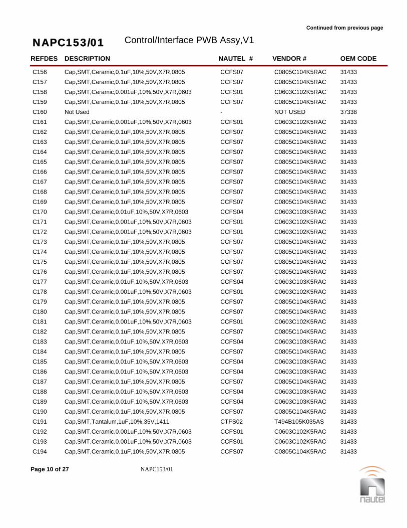
Continued from previous page
NAPC153/01 Control/Interface PWB Assy,V1
REFDES NAUTEL #DESCRIPTION VENDOR # OEM CODE
C156 CCFS07Cap,SMT,Ceramic,0.1uF,10%,50V,X7R,0805 C0805C104K5RAC 31433
C157 CCFS07Cap,SMT,Ceramic,0.1uF,10%,50V,X7R,0805 C0805C104K5RAC 31433
C158 CCFS01Cap,SMT,Ceramic,0.001uF,10%,50V,X7R,0603 C0603C102K5RAC 31433 C159 CCFS07Cap,SMT,Ceramic,0.1uF,10%,50V,X7R,0805 C0805C104K5RAC 31433
C160 -Not Used NOT USED 37338
C161 CCFS01Cap,SMT,Ceramic,0.001uF,10%,50V,X7R,0603 C0603C102K5RAC 31433 C162 CCFS07Cap,SMT,Ceramic,0.1uF,10%,50V,X7R,0805 C0805C104K5RAC 31433
C163 CCFS07Cap,SMT,Ceramic,0.1uF,10%,50V,X7R,0805 C0805C104K5RAC 31433
C164 CCFS07Cap,SMT,Ceramic,0.1uF,10%,50V,X7R,0805 C0805C104K5RAC 31433 C165 CCFS07Cap,SMT,Ceramic,0.1uF,10%,50V,X7R,0805 C0805C104K5RAC 31433
C166 CCFS07Cap,SMT,Ceramic,0.1uF,10%,50V,X7R,0805 C0805C104K5RAC 31433 C167 CCFS07Cap,SMT,Ceramic,0.1uF,10%,50V,X7R,0805 C0805C104K5RAC 31433
C168 CCFS07Cap,SMT,Ceramic,0.1uF,10%,50V,X7R,0805 C0805C104K5RAC 31433
C169 CCFS07Cap,SMT,Ceramic,0.1uF,10%,50V,X7R,0805 C0805C104K5RAC 31433 C170 CCFS04Cap,SMT,Ceramic,0.01uF,10%,50V,X7R,0603 C0603C103K5RAC 31433
C171 CCFS01Cap,SMT,Ceramic,0.001uF,10%,50V,X7R,0603 C0603C102K5RAC 31433
C172 CCFS01Cap,SMT,Ceramic,0.001uF,10%,50V,X7R,0603 C0603C102K5RAC 31433 C173 CCFS07Cap,SMT,Ceramic,0.1uF,10%,50V,X7R,0805 C0805C104K5RAC 31433
C174 CCFS07Cap,SMT,Ceramic,0.1uF,10%,50V,X7R,0805 C0805C104K5RAC 31433
C175 CCFS07Cap,SMT,Ceramic,0.1uF,10%,50V,X7R,0805 C0805C104K5RAC 31433 C176 CCFS07Cap,SMT,Ceramic,0.1uF,10%,50V,X7R,0805 C0805C104K5RAC 31433
C177 CCFS04Cap,SMT,Ceramic,0.01uF,10%,50V,X7R,0603 C0603C103K5RAC 31433
C178 CCFS01Cap,SMT,Ceramic,0.001uF,10%,50V,X7R,0603 C0603C102K5RAC 31433 C179 CCFS07Cap,SMT,Ceramic,0.1uF,10%,50V,X7R,0805 C0805C104K5RAC 31433
C180 CCFS07Cap,SMT,Ceramic,0.1uF,10%,50V,X7R,0805 C0805C104K5RAC 31433 C181 CCFS01Cap,SMT,Ceramic,0.001uF,10%,50V,X7R,0603 C0603C102K5RAC 31433
C182 CCFS07Cap,SMT,Ceramic,0.1uF,10%,50V,X7R,0805 C0805C104K5RAC 31433
C183 CCFS04Cap,SMT,Ceramic,0.01uF,10%,50V,X7R,0603 C0603C103K5RAC 31433 C184 CCFS07Cap,SMT,Ceramic,0.1uF,10%,50V,X7R,0805 C0805C104K5RAC 31433
C185 CCFS04Cap,SMT,Ceramic,0.01uF,10%,50V,X7R,0603 C0603C103K5RAC 31433
C186 CCFS04Cap,SMT,Ceramic,0.01uF,10%,50V,X7R,0603 C0603C103K5RAC 31433 C187 CCFS07Cap,SMT,Ceramic,0.1uF,10%,50V,X7R,0805 C0805C104K5RAC 31433
C188 CCFS04Cap,SMT,Ceramic,0.01uF,10%,50V,X7R,0603 C0603C103K5RAC 31433
C189 CCFS04Cap,SMT,Ceramic,0.01uF,10%,50V,X7R,0603 C0603C103K5RAC 31433 C190 CCFS07Cap,SMT,Ceramic,0.1uF,10%,50V,X7R,0805 C0805C104K5RAC 31433
C191 CTFS02Cap,SMT,Tantalum,1uF,10%,35V,1411 T494B105K035AS 31433
C192 CCFS01Cap,SMT,Ceramic,0.001uF,10%,50V,X7R,0603 C0603C102K5RAC 31433 C193 CCFS01Cap,SMT,Ceramic,0.001uF,10%,50V,X7R,0603 C0603C102K5RAC 31433
C194 CCFS07Cap,SMT,Ceramic,0.1uF,10%,50V,X7R,0805 C0805C104K5RAC 31433
Page 10 of 27 NAPC153/01

Continued from previous page
NAPC153/01 Control/Interface PWB Assy,V1
REFDES NAUTEL #DESCRIPTION VENDOR # OEM CODE
C195 CCFS04Cap,SMT,Ceramic,0.01uF,10%,50V,X7R,0603 C0603C103K5RAC 31433
C196 CCFS04Cap,SMT,Ceramic,0.01uF,10%,50V,X7R,0603 C0603C103K5RAC 31433
C197 CCFS07Cap,SMT,Ceramic,0.1uF,10%,50V,X7R,0805 C0805C104K5RAC 31433 C198 CCFS07Cap,SMT,Ceramic,0.1uF,10%,50V,X7R,0805 C0805C104K5RAC 31433
C199 CCFS04Cap,SMT,Ceramic,0.01uF,10%,50V,X7R,0603 C0603C103K5RAC 31433
C200 CCFS07Cap,SMT,Ceramic,0.1uF,10%,50V,X7R,0805 C0805C104K5RAC 31433 C201 CCFS61Cap,SMT,Ceramic,0.001uF,10%,100V,X7R,0805 C0805C102K1RACTU 31433
C202 CCFS61Cap,SMT,Ceramic,0.001uF,10%,100V,X7R,0805 C0805C102K1RACTU 31433
C203 CCFS61Cap,SMT,Ceramic,0.001uF,10%,100V,X7R,0805 C0805C102K1RACTU 31433 C204 CCFS07Cap,SMT,Ceramic,0.1uF,10%,50V,X7R,0805 C0805C104K5RAC 31433
C205 CCFS07Cap,SMT,Ceramic,0.1uF,10%,50V,X7R,0805 C0805C104K5RAC 31433 C206 CCFS23Cap,SMT,Ceramic,18pF,2%,50V,C0G,0603 C0603C180G5GAC 31433
C207 CCFS23Cap,SMT,Ceramic,18pF,2%,50V,C0G,0603 C0603C180G5GAC 31433
C208 CCFS04Cap,SMT,Ceramic,0.01uF,10%,50V,X7R,0603 C0603C103K5RAC 31433 C209 CCFS01Cap,SMT,Ceramic,0.001uF,10%,50V,X7R,0603 C0603C102K5RAC 31433
C210 CCFS07Cap,SMT,Ceramic,0.1uF,10%,50V,X7R,0805 C0805C104K5RAC 31433
C211 CCFS07Cap,SMT,Ceramic,0.1uF,10%,50V,X7R,0805 C0805C104K5RAC 31433 C212 CCFS61Cap,SMT,Ceramic,0.001uF,10%,100V,X7R,0805 C0805C102K1RACTU 31433
C213 CCFS04Cap,SMT,Ceramic,0.01uF,10%,50V,X7R,0603 C0603C103K5RAC 31433
C214 CCFS07Cap,SMT,Ceramic,0.1uF,10%,50V,X7R,0805 C0805C104K5RAC 31433 C215 CCFS61Cap,SMT,Ceramic,0.001uF,10%,100V,X7R,0805 C0805C102K1RACTU 31433
C216 CCFS61Cap,SMT,Ceramic,0.001uF,10%,100V,X7R,0805 C0805C102K1RACTU 31433
C217 CCFS04Cap,SMT,Ceramic,0.01uF,10%,50V,X7R,0603 C0603C103K5RAC 31433 C218 CCFS04Cap,SMT,Ceramic,0.01uF,10%,50V,X7R,0603 C0603C103K5RAC 31433
C219 CCFS07Cap,SMT,Ceramic,0.1uF,10%,50V,X7R,0805 C0805C104K5RAC 31433 C220 CCFS61Cap,SMT,Ceramic,0.001uF,10%,100V,X7R,0805 C0805C102K1RACTU 31433
C221 CCFS61Cap,SMT,Ceramic,0.001uF,10%,100V,X7R,0805 C0805C102K1RACTU 31433
C222 CCFS61Cap,SMT,Ceramic,0.001uF,10%,100V,X7R,0805 C0805C102K1RACTU 31433 C223 CCFS04Cap,SMT,Ceramic,0.01uF,10%,50V,X7R,0603 C0603C103K5RAC 31433
C224 CCFS61Cap,SMT,Ceramic,0.001uF,10%,100V,X7R,0805 C0805C102K1RACTU 31433
C225 CCFS61Cap,SMT,Ceramic,0.001uF,10%,100V,X7R,0805 C0805C102K1RACTU 31433 C226 CCFS61Cap,SMT,Ceramic,0.001uF,10%,100V,X7R,0805 C0805C102K1RACTU 31433
C227 CCFS61Cap,SMT,Ceramic,0.001uF,10%,100V,X7R,0805 C0805C102K1RACTU 31433
C228 CCFS04Cap,SMT,Ceramic,0.01uF,10%,50V,X7R,0603 C0603C103K5RAC 31433 C229 CCFS04Cap,SMT,Ceramic,0.01uF,10%,50V,X7R,0603 C0603C103K5RAC 31433
C230 CCFS07Cap,SMT,Ceramic,0.1uF,10%,50V,X7R,0805 C0805C104K5RAC 31433
C231 CCFS07Cap,SMT,Ceramic,0.1uF,10%,50V,X7R,0805 C0805C104K5RAC 31433 C232 CCFS07Cap,SMT,Ceramic,0.1uF,10%,50V,X7R,0805 C0805C104K5RAC 31433
C233 CCFS07Cap,SMT,Ceramic,0.1uF,10%,50V,X7R,0805 C0805C104K5RAC 31433
Page 11 of 27 NAPC153/01

Continued from previous page
NAPC153/01 Control/Interface PWB Assy,V1
REFDES NAUTEL #DESCRIPTION VENDOR # OEM CODE
C234 CCFS07Cap,SMT,Ceramic,0.1uF,10%,50V,X7R,0805 C0805C104K5RAC 31433
C235 CCFS07Cap,SMT,Ceramic,0.1uF,10%,50V,X7R,0805 C0805C104K5RAC 31433
C236 -Not Used NOT USED 37338 C237 CCFS04Cap,SMT,Ceramic,0.01uF,10%,50V,X7R,0603 C0603C103K5RAC 31433
C238 CCFS61Cap,SMT,Ceramic,0.001uF,10%,100V,X7R,0805 C0805C102K1RACTU 31433
C239 -Not Used NOT USED 37338 C240 CCFS04Cap,SMT,Ceramic,0.01uF,10%,50V,X7R,0603 C0603C103K5RAC 31433
C241 CCFS07Cap,SMT,Ceramic,0.1uF,10%,50V,X7R,0805 C0805C104K5RAC 31433
C242 CCFS04Cap,SMT,Ceramic,0.01uF,10%,50V,X7R,0603 C0603C103K5RAC 31433 C243 CCFS61Cap,SMT,Ceramic,0.001uF,10%,100V,X7R,0805 C0805C102K1RACTU 31433
C244 CCFS61Cap,SMT,Ceramic,0.001uF,10%,100V,X7R,0805 C0805C102K1RACTU 31433 C245 CCFS61Cap,SMT,Ceramic,0.001uF,10%,100V,X7R,0805 C0805C102K1RACTU 31433
C246 CCFS07Cap,SMT,Ceramic,0.1uF,10%,50V,X7R,0805 C0805C104K5RAC 31433
C247 CCFS04Cap,SMT,Ceramic,0.01uF,10%,50V,X7R,0603 C0603C103K5RAC 31433 C248 CCFS07Cap,SMT,Ceramic,0.1uF,10%,50V,X7R,0805 C0805C104K5RAC 31433
C249 CCFS07Cap,SMT,Ceramic,0.1uF,10%,50V,X7R,0805 C0805C104K5RAC 31433
C250 CCFS04Cap,SMT,Ceramic,0.01uF,10%,50V,X7R,0603 C0603C103K5RAC 31433 C251 CCFS04Cap,SMT,Ceramic,0.01uF,10%,50V,X7R,0603 C0603C103K5RAC 31433
C252 CCFS07Cap,SMT,Ceramic,0.1uF,10%,50V,X7R,0805 C0805C104K5RAC 31433
C253 CCFS07Cap,SMT,Ceramic,0.1uF,10%,50V,X7R,0805 C0805C104K5RAC 31433 C254 CCFS07Cap,SMT,Ceramic,0.1uF,10%,50V,X7R,0805 C0805C104K5RAC 31433
C255 CCFS04Cap,SMT,Ceramic,0.01uF,10%,50V,X7R,0603 C0603C103K5RAC 31433
C256 CCFS01Cap,SMT,Ceramic,0.001uF,10%,50V,X7R,0603 C0603C102K5RAC 31433 C257 CCFS04Cap,SMT,Ceramic,0.01uF,10%,50V,X7R,0603 C0603C103K5RAC 31433
C258 CTFS03Cap,SMT,Tantalum,10uF,10%,35V,2917 T494D106K035AS 31433 C259 CCFS04Cap,SMT,Ceramic,0.01uF,10%,50V,X7R,0603 C0603C103K5RAC 31433
C260 CCFS07Cap,SMT,Ceramic,0.1uF,10%,50V,X7R,0805 C0805C104K5RAC 31433
C261 CCFS07Cap,SMT,Ceramic,0.1uF,10%,50V,X7R,0805 C0805C104K5RAC 31433 C262 CCFS07Cap,SMT,Ceramic,0.1uF,10%,50V,X7R,0805 C0805C104K5RAC 31433
C263 CCFS07Cap,SMT,Ceramic,0.1uF,10%,50V,X7R,0805 C0805C104K5RAC 31433
C264 CCFS04Cap,SMT,Ceramic,0.01uF,10%,50V,X7R,0603 C0603C103K5RAC 31433 C265 CTFS03Cap,SMT,Tantalum,10uF,10%,35V,2917 T494D106K035AS 31433
C266 CCFS07Cap,SMT,Ceramic,0.1uF,10%,50V,X7R,0805 C0805C104K5RAC 31433
C267 CCFS04Cap,SMT,Ceramic,0.01uF,10%,50V,X7R,0603 C0603C103K5RAC 31433 C268 CCFS04Cap,SMT,Ceramic,0.01uF,10%,50V,X7R,0603 C0603C103K5RAC 31433
C269 CCFS01Cap,SMT,Ceramic,0.001uF,10%,50V,X7R,0603 C0603C102K5RAC 31433
C270 CTFS03Cap,SMT,Tantalum,10uF,10%,35V,2917 T494D106K035AS 31433 C271 CCFS07Cap,SMT,Ceramic,0.1uF,10%,50V,X7R,0805 C0805C104K5RAC 31433
C272 CCFS07Cap,SMT,Ceramic,0.1uF,10%,50V,X7R,0805 C0805C104K5RAC 31433
Page 12 of 27 NAPC153/01

Continued from previous page
NAPC153/01 Control/Interface PWB Assy,V1
REFDES NAUTEL #DESCRIPTION VENDOR # OEM CODE
C273 CCFS04Cap,SMT,Ceramic,0.01uF,10%,50V,X7R,0603 C0603C103K5RAC 31433
C274 CCFS07Cap,SMT,Ceramic,0.1uF,10%,50V,X7R,0805 C0805C104K5RAC 31433
C275 -Not Used NOT USED 37338 C276 CCFS01Cap,SMT,Ceramic,0.001uF,10%,50V,X7R,0603 C0603C102K5RAC 31433
C277 CCFS01Cap,SMT,Ceramic,0.001uF,10%,50V,X7R,0603 C0603C102K5RAC 31433
C278 CCFS01Cap,SMT,Ceramic,0.001uF,10%,50V,X7R,0603 C0603C102K5RAC 31433 C279 CCFS04Cap,SMT,Ceramic,0.01uF,10%,50V,X7R,0603 C0603C103K5RAC 31433
C280 CTFS01Cap,SMT,Tantalum,10uF,10%,16V,1411 T494B106K016AS 31433
C281 CCFS07Cap,SMT,Ceramic,0.1uF,10%,50V,X7R,0805 C0805C104K5RAC 31433 C282 CCFS04Cap,SMT,Ceramic,0.01uF,10%,50V,X7R,0603 C0603C103K5RAC 31433
C283 CCFS07Cap,SMT,Ceramic,0.1uF,10%,50V,X7R,0805 C0805C104K5RAC 31433 C284 CCFS01Cap,SMT,Ceramic,0.001uF,10%,50V,X7R,0603 C0603C102K5RAC 31433
C285 CCFS07Cap,SMT,Ceramic,0.1uF,10%,50V,X7R,0805 C0805C104K5RAC 31433
C286 CCFS07Cap,SMT,Ceramic,0.1uF,10%,50V,X7R,0805 C0805C104K5RAC 31433 C287 CCFS07Cap,SMT,Ceramic,0.1uF,10%,50V,X7R,0805 C0805C104K5RAC 31433
C288 CCFS07Cap,SMT,Ceramic,0.1uF,10%,50V,X7R,0805 C0805C104K5RAC 31433
C289 CCFS04Cap,SMT,Ceramic,0.01uF,10%,50V,X7R,0603 C0603C103K5RAC 31433 C290 CCFS04Cap,SMT,Ceramic,0.01uF,10%,50V,X7R,0603 C0603C103K5RAC 31433
C291 CTFS03Cap,SMT,Tantalum,10uF,10%,35V,2917 T494D106K035AS 31433
C292 CTFS03Cap,SMT,Tantalum,10uF,10%,35V,2917 T494D106K035AS 31433 C293 CTFS03Cap,SMT,Tantalum,10uF,10%,35V,2917 T494D106K035AS 31433
C294 -Not Used NOT USED 37338
C295 CCFS07Cap,SMT,Ceramic,0.1uF,10%,50V,X7R,0805 C0805C104K5RAC 31433 C296 CCFS04Cap,SMT,Ceramic,0.01uF,10%,50V,X7R,0603 C0603C103K5RAC 31433
CR01 QR57Transient Voltage Suppressor,SMT,15V SMBJ15CA(STATIC)RoHS
75915
CR02 QR57Transient Voltage Suppressor,SMT,15V SMBJ15CA(STATIC)RoHS
75915
CR03 QR57Transient Voltage Suppressor,SMT,15V SMBJ15CA(STATIC)RoHS
75915
CR04 QR57Transient Voltage Suppressor,SMT,15V SMBJ15CA(STATIC)RoHS
75915
CR05 QDZS04Diode,SMT,Zener,39V,5%,3W,SMB 1SMB5939BT3 04713 CR06 QDZS04Diode,SMT,Zener,39V,5%,3W,SMB 1SMB5939BT3 04713
CR07 QR57Transient Voltage Suppressor,SMT,15V SMBJ15CA(STATIC)RoHS
75915
CR08 QR57Transient Voltage Suppressor,SMT,15V SMBJ15CA(STATIC)RoHS
75915
CR09 QDRS01Diode,SMT,Switching,250V,0.2A,SOD-323 BAS21HT1(STATIC) 04713
CR10 QDZS04Diode,SMT,Zener,39V,5%,3W,SMB 1SMB5939BT3 04713 CR11 QK09Diode, Schottky 1N5711 (STATIC) 50434
CR12 QDSS01Diode,SMT,Schottky,30V,0.2A,SOD-323 BAT54HT1(STATIC) 04713
Page 13 of 27 NAPC153/01
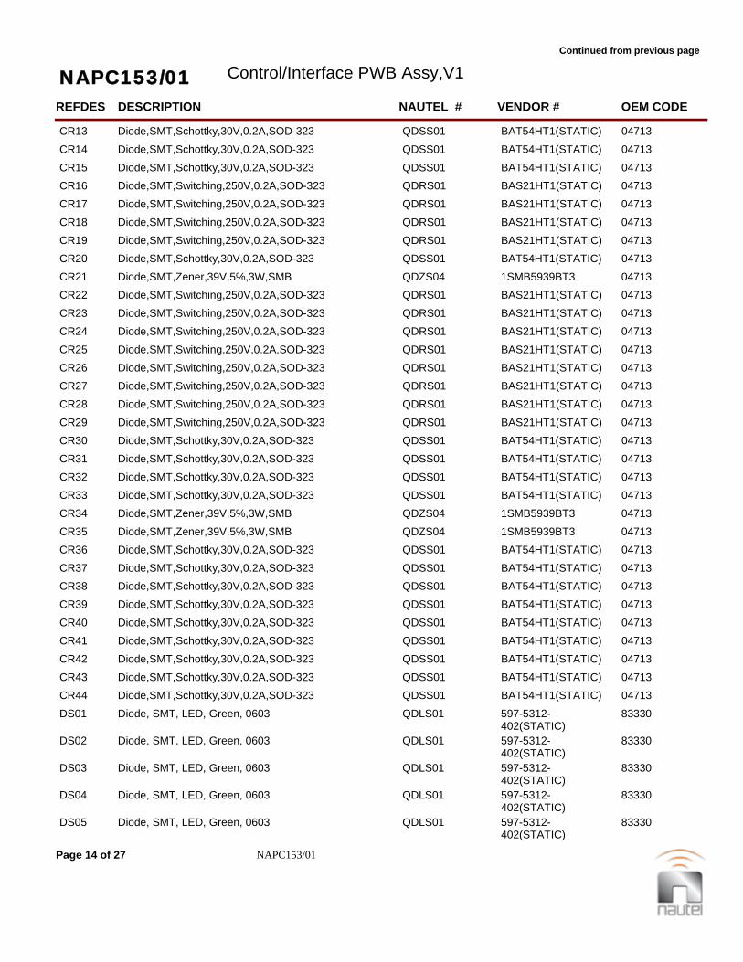
Continued from previous page
NAPC153/01 Control/Interface PWB Assy,V1
REFDES NAUTEL #DESCRIPTION VENDOR # OEM CODE
CR13 QDSS01Diode,SMT,Schottky,30V,0.2A,SOD-323 BAT54HT1(STATIC) 04713
CR14 QDSS01Diode,SMT,Schottky,30V,0.2A,SOD-323 BAT54HT1(STATIC) 04713
CR15 QDSS01Diode,SMT,Schottky,30V,0.2A,SOD-323 BAT54HT1(STATIC) 04713 CR16 QDRS01Diode,SMT,Switching,250V,0.2A,SOD-323 BAS21HT1(STATIC) 04713
CR17 QDRS01Diode,SMT,Switching,250V,0.2A,SOD-323 BAS21HT1(STATIC) 04713
CR18 QDRS01Diode,SMT,Switching,250V,0.2A,SOD-323 BAS21HT1(STATIC) 04713 CR19 QDRS01Diode,SMT,Switching,250V,0.2A,SOD-323 BAS21HT1(STATIC) 04713
CR20 QDSS01Diode,SMT,Schottky,30V,0.2A,SOD-323 BAT54HT1(STATIC) 04713
CR21 QDZS04Diode,SMT,Zener,39V,5%,3W,SMB 1SMB5939BT3 04713 CR22 QDRS01Diode,SMT,Switching,250V,0.2A,SOD-323 BAS21HT1(STATIC) 04713
CR23 QDRS01Diode,SMT,Switching,250V,0.2A,SOD-323 BAS21HT1(STATIC) 04713 CR24 QDRS01Diode,SMT,Switching,250V,0.2A,SOD-323 BAS21HT1(STATIC) 04713
CR25 QDRS01Diode,SMT,Switching,250V,0.2A,SOD-323 BAS21HT1(STATIC) 04713
CR26 QDRS01Diode,SMT,Switching,250V,0.2A,SOD-323 BAS21HT1(STATIC) 04713 CR27 QDRS01Diode,SMT,Switching,250V,0.2A,SOD-323 BAS21HT1(STATIC) 04713
CR28 QDRS01Diode,SMT,Switching,250V,0.2A,SOD-323 BAS21HT1(STATIC) 04713
CR29 QDRS01Diode,SMT,Switching,250V,0.2A,SOD-323 BAS21HT1(STATIC) 04713 CR30 QDSS01Diode,SMT,Schottky,30V,0.2A,SOD-323 BAT54HT1(STATIC) 04713
CR31 QDSS01Diode,SMT,Schottky,30V,0.2A,SOD-323 BAT54HT1(STATIC) 04713
CR32 QDSS01Diode,SMT,Schottky,30V,0.2A,SOD-323 BAT54HT1(STATIC) 04713 CR33 QDSS01Diode,SMT,Schottky,30V,0.2A,SOD-323 BAT54HT1(STATIC) 04713
CR34 QDZS04Diode,SMT,Zener,39V,5%,3W,SMB 1SMB5939BT3 04713
CR35 QDZS04Diode,SMT,Zener,39V,5%,3W,SMB 1SMB5939BT3 04713 CR36 QDSS01Diode,SMT,Schottky,30V,0.2A,SOD-323 BAT54HT1(STATIC) 04713
CR37 QDSS01Diode,SMT,Schottky,30V,0.2A,SOD-323 BAT54HT1(STATIC) 04713 CR38 QDSS01Diode,SMT,Schottky,30V,0.2A,SOD-323 BAT54HT1(STATIC) 04713
CR39 QDSS01Diode,SMT,Schottky,30V,0.2A,SOD-323 BAT54HT1(STATIC) 04713
CR40 QDSS01Diode,SMT,Schottky,30V,0.2A,SOD-323 BAT54HT1(STATIC) 04713 CR41 QDSS01Diode,SMT,Schottky,30V,0.2A,SOD-323 BAT54HT1(STATIC) 04713
CR42 QDSS01Diode,SMT,Schottky,30V,0.2A,SOD-323 BAT54HT1(STATIC) 04713
CR43 QDSS01Diode,SMT,Schottky,30V,0.2A,SOD-323 BAT54HT1(STATIC) 04713 CR44 QDSS01Diode,SMT,Schottky,30V,0.2A,SOD-323 BAT54HT1(STATIC) 04713
DS01 QDLS01Diode, SMT, LED, Green, 0603 597-5312-402(STATIC)
83330
DS02 QDLS01Diode, SMT, LED, Green, 0603 597-5312-402(STATIC)
83330
DS03 QDLS01Diode, SMT, LED, Green, 0603 597-5312-402(STATIC)
83330
DS04 QDLS01Diode, SMT, LED, Green, 0603 597-5312-402(STATIC)
83330
DS05 QDLS01Diode, SMT, LED, Green, 0603 597-5312-402(STATIC)
83330
Page 14 of 27 NAPC153/01

Continued from previous page
NAPC153/01 Control/Interface PWB Assy,V1
REFDES NAUTEL #DESCRIPTION VENDOR # OEM CODE
DS06 QDLS01Diode, SMT, LED, Green, 0603 597-5312-402(STATIC)
83330
E01 JQ15Conn, Post Shunt, 2 Pos, .10 Centreline 390088-2 09482
E02 JQ15Conn, Post Shunt, 2 Pos, .10 Centreline 390088-2 09482 E03 HAC48Terminal, Screw, 10-32 1293 91833
E04 HAC48Terminal, Screw, 10-32 1293 91833 E05 HR26Connector, Quick-Dis, M,1/4 Tab, PWB 1287 91833
E06 HR26Connector, Quick-Dis, M,1/4 Tab, PWB 1287 91833
E07 HR26Connector, Quick-Dis, M,1/4 Tab, PWB 1287 91833 J01 JM44Conn, Jack, RJ45, PWB Mount 556591-1 09482
J02 JR51Terminal Block,2-pos,PWB Mount 1803277(ROHS) PHOENIX
J03 JT79Connector,Dual,D-Sub,M/F,37-pin,Rt Agl, PWB 663-037-264-036(RoHS)
EDAC
J04 JR51Terminal Block,2-pos,PWB Mount 1803277(ROHS) PHOENIX
J05 JQ16Conn, Header, SIP,12 Pin Breakawy,.10 Ctr 1-103185-2 09482 J06 JF47Conn, Header,Square Post,Gold,Dual,40-pin 4-102973-0 09482
J07 JU29MTA, Square Post Header Assy,POL&N,2-pin 640445-2 00779
J08 JQ54Conn, Header, Ribbon Cbl, 10-Pin 103308-1 00779 J09 JU24MTA, Keyed Square Post HeaderAssy, 8 pin 647123-8 00779
J10 JQ16Conn, Header, SIP,12 Pin Breakawy,.10 Ctr 1-103185-2 09482
J11 JS50Conn, Socket, D-Sub, 9-Pin,Vertical PWB 164A16669X C3057 J12 JQ55Conn, Header, Ribbon Cbl, 20Pin 103308-5 00779
J13 JT65Conn, Pin Header,3-Pin,Mate-N-Lok, Vert 641966-1 09482
J14 JT65Conn, Pin Header,3-Pin,Mate-N-Lok, Vert 641966-1 09482 J15 JU24MTA, Keyed Square Post HeaderAssy, 8 pin 647123-8 00779
J16 JU25MTA, Keyed Square Post HeaderAssy, 4 pin 647123-4 00779 J17 JT37Conn, Coax, Recept, PWB Mt, RG188 TMP-J01X-V6 TAIKO
J18 JT37Conn, Coax, Recept, PWB Mt, RG188 TMP-J01X-V6 TAIKO
J19 JT37Conn, Coax, Recept, PWB Mt, RG188 TMP-J01X-V6 TAIKO J20 JT37Conn, Coax, Recept, PWB Mt, RG188 TMP-J01X-V6 TAIKO
J21 JF35Conn, BNC, Recept, PWB Mt R141426161 0GP12
J22 JU24MTA, Keyed Square Post HeaderAssy, 8 pin 647123-8 00779 J23 JU25MTA, Keyed Square Post HeaderAssy, 4 pin 647123-4 00779
K01 KC07Relay, 12Vdc Coil, 2PDT, 1A DF2E-DC12V 61529
L01 LCFS01Inductor, SMT, Choke, 600ohms,2A, 0805 ILHB0805RK601V 56845 L02 LCFS01Inductor, SMT, Choke, 600ohms,2A, 0805 ILHB0805RK601V 56845
L03 LCFS01Inductor, SMT, Choke, 600ohms,2A, 0805 ILHB0805RK601V 56845
L04 LCFS01Inductor, SMT, Choke, 600ohms,2A, 0805 ILHB0805RK601V 56845 L05 LCFS01Inductor, SMT, Choke, 600ohms,2A, 0805 ILHB0805RK601V 56845
L06 LCFS01Inductor, SMT, Choke, 600ohms,2A, 0805 ILHB0805RK601V 56845
Page 15 of 27 NAPC153/01

Continued from previous page
NAPC153/01 Control/Interface PWB Assy,V1
REFDES NAUTEL #DESCRIPTION VENDOR # OEM CODE
L07 LCFS01Inductor, SMT, Choke, 600ohms,2A, 0805 ILHB0805RK601V 56845
L08 LCFS01Inductor, SMT, Choke, 600ohms,2A, 0805 ILHB0805RK601V 56845
L09 LCFS01Inductor, SMT, Choke, 600ohms,2A, 0805 ILHB0805RK601V 56845 L10 LCFS01Inductor, SMT, Choke, 600ohms,2A, 0805 ILHB0805RK601V 56845
L11 LCFS01Inductor, SMT, Choke, 600ohms,2A, 0805 ILHB0805RK601V 56845
L12 LCFS01Inductor, SMT, Choke, 600ohms,2A, 0805 ILHB0805RK601V 56845 L13 LCFS01Inductor, SMT, Choke, 600ohms,2A, 0805 ILHB0805RK601V 56845
L14 LCFS01Inductor, SMT, Choke, 600ohms,2A, 0805 ILHB0805RK601V 56845
L15 LCFS01Inductor, SMT, Choke, 600ohms,2A, 0805 ILHB0805RK601V 56845 L16 LCFS01Inductor, SMT, Choke, 600ohms,2A, 0805 ILHB0805RK601V 56845
L17 LCFS01Inductor, SMT, Choke, 600ohms,2A, 0805 ILHB0805RK601V 56845 L18 LCFS01Inductor, SMT, Choke, 600ohms,2A, 0805 ILHB0805RK601V 56845
L19 LCFS01Inductor, SMT, Choke, 600ohms,2A, 0805 ILHB0805RK601V 56845
L20 LCFS01Inductor, SMT, Choke, 600ohms,2A, 0805 ILHB0805RK601V 56845 L21 LCFS01Inductor, SMT, Choke, 600ohms,2A, 0805 ILHB0805RK601V 56845
L22 LCFS01Inductor, SMT, Choke, 600ohms,2A, 0805 ILHB0805RK601V 56845
L23 LCFS01Inductor, SMT, Choke, 600ohms,2A, 0805 ILHB0805RK601V 56845 L24 LCFS01Inductor, SMT, Choke, 600ohms,2A, 0805 ILHB0805RK601V 56845
L25 LCFS01Inductor, SMT, Choke, 600ohms,2A, 0805 ILHB0805RK601V 56845
L26 LCFS01Inductor, SMT, Choke, 600ohms,2A, 0805 ILHB0805RK601V 56845 L27 LCFS01Inductor, SMT, Choke, 600ohms,2A, 0805 ILHB0805RK601V 56845
L28 LCFS01Inductor, SMT, Choke, 600ohms,2A, 0805 ILHB0805RK601V 56845
L29 LCFS01Inductor, SMT, Choke, 600ohms,2A, 0805 ILHB0805RK601V 56845 L30 LCFS01Inductor, SMT, Choke, 600ohms,2A, 0805 ILHB0805RK601V 56845
L31 LCFS01Inductor, SMT, Choke, 600ohms,2A, 0805 ILHB0805RK601V 56845 L32 LCFS01Inductor, SMT, Choke, 600ohms,2A, 0805 ILHB0805RK601V 56845
L33 LCFS01Inductor, SMT, Choke, 600ohms,2A, 0805 ILHB0805RK601V 56845
L34 LCFS01Inductor, SMT, Choke, 600ohms,2A, 0805 ILHB0805RK601V 56845 L35 LCFS01Inductor, SMT, Choke, 600ohms,2A, 0805 ILHB0805RK601V 56845
L36 LCFS01Inductor, SMT, Choke, 600ohms,2A, 0805 ILHB0805RK601V 56845
L37 LCFS01Inductor, SMT, Choke, 600ohms,2A, 0805 ILHB0805RK601V 56845 L38 LCFS01Inductor, SMT, Choke, 600ohms,2A, 0805 ILHB0805RK601V 56845
L39 LCFS01Inductor, SMT, Choke, 600ohms,2A, 0805 ILHB0805RK601V 56845
L40 LCFS01Inductor, SMT, Choke, 600ohms,2A, 0805 ILHB0805RK601V 56845 L41 LCFS01Inductor, SMT, Choke, 600ohms,2A, 0805 ILHB0805RK601V 56845
L42 LCFS01Inductor, SMT, Choke, 600ohms,2A, 0805 ILHB0805RK601V 56845
L43 LCFS01Inductor, SMT, Choke, 600ohms,2A, 0805 ILHB0805RK601V 56845 L44 LCFS01Inductor, SMT, Choke, 600ohms,2A, 0805 ILHB0805RK601V 56845
L45 LCFS01Inductor, SMT, Choke, 600ohms,2A, 0805 ILHB0805RK601V 56845
Page 16 of 27 NAPC153/01

Continued from previous page
NAPC153/01 Control/Interface PWB Assy,V1
REFDES NAUTEL #DESCRIPTION VENDOR # OEM CODE
L46 LCFS01Inductor, SMT, Choke, 600ohms,2A, 0805 ILHB0805RK601V 56845
L47 LCFS01Inductor, SMT, Choke, 600ohms,2A, 0805 ILHB0805RK601V 56845
L48 LCFS01Inductor, SMT, Choke, 600ohms,2A, 0805 ILHB0805RK601V 56845 L49 LCFS01Inductor, SMT, Choke, 600ohms,2A, 0805 ILHB0805RK601V 56845
L50 LCFS01Inductor, SMT, Choke, 600ohms,2A, 0805 ILHB0805RK601V 56845
L51 LCFS01Inductor, SMT, Choke, 600ohms,2A, 0805 ILHB0805RK601V 56845 L52 LCFS01Inductor, SMT, Choke, 600ohms,2A, 0805 ILHB0805RK601V 56845
L53 LCFS01Inductor, SMT, Choke, 600ohms,2A, 0805 ILHB0805RK601V 56845
L54 LCFS01Inductor, SMT, Choke, 600ohms,2A, 0805 ILHB0805RK601V 56845 L55 LCFS01Inductor, SMT, Choke, 600ohms,2A, 0805 ILHB0805RK601V 56845
L56 LCFS01Inductor, SMT, Choke, 600ohms,2A, 0805 ILHB0805RK601V 56845 L57 LA16Inductor, Choke, 2.5 Turns, JMtl 82-152-J 33062
L58 LCFS01Inductor, SMT, Choke, 600ohms,2A, 0805 ILHB0805RK601V 56845
Q01 QN53Transistor,SMT,MOSFET,N-Channel,60V,115mA,SOT-23
2N7002LT1G(STATIC)(ROHS)
1MQ07
Q02 QR52Transistor, FET, N Channel, Plas IRF540N(STATIC) 81483
Q03 QBNS01Transistor,SMT,NPN,Switch/Amp,SOT-23 MMBT4401LT1(STATIC)
04713
R001 RFFS53Resistor,SMT,MF,18.2Kohms,1%,1/10W,0603 RK73H1JLTD1822F 59124
R002 RFFS65Resistor,SMT,MF,182Kohms,1%,1/10W,0603 RK73H1JLTD1823F 59124
R003 RFFS36Resistor,SMT,MF,681ohms,1%,1/10W,0603 RK73H1JLTD6810F 59124 R004 RAD17Resistor, SMT, MF, 221 Ohms,1% 1/4W RK73H2BL2210F 59124
R005 RAD17Resistor, SMT, MF, 221 Ohms,1% 1/4W RK73H2BL2210F 59124
R006 RFFS36Resistor,SMT,MF,681ohms,1%,1/10W,0603 RK73H1JLTD6810F 59124 R007 RFFS50Resistor,SMT,MF,10.0Kohms,1%,1/10W,0603 RK73H1JLTD1002F 59124
R008 RFFS50Resistor,SMT,MF,10.0Kohms,1%,1/10W,0603 RK73H1JLTD1002F 59124 R009 RFFS50Resistor,SMT,MF,10.0Kohms,1%,1/10W,0603 RK73H1JLTD1002F 59124
R010 RFFS50Resistor,SMT,MF,10.0Kohms,1%,1/10W,0603 RK73H1JLTD1002F 59124
R011 RFFS26Resistor,SMT,MF,100ohms,1%,1/10W,0603 RK73H1JLTD1000F 59124 R012 RFFS26Resistor,SMT,MF,100ohms,1%,1/10W,0603 RK73H1JLTD1000F 59124
R013 RFFS50Resistor,SMT,MF,10.0Kohms,1%,1/10W,0603 RK73H1JLTD1002F 59124
R014 RFFS50Resistor,SMT,MF,10.0Kohms,1%,1/10W,0603 RK73H1JLTD1002F 59124 R015 RFFS50Resistor,SMT,MF,10.0Kohms,1%,1/10W,0603 RK73H1JLTD1002F 59124
R016 RFFS50Resistor,SMT,MF,10.0Kohms,1%,1/10W,0603 RK73H1JLTD1002F 59124
R017 RFFS50Resistor,SMT,MF,10.0Kohms,1%,1/10W,0603 RK73H1JLTD1002F 59124 R018 RFFS36Resistor,SMT,MF,681ohms,1%,1/10W,0603 RK73H1JLTD6810F 59124
R019 RFFS01Resistor,SMT,MF,0.0ohms,Jumper,0603 RK73Z1JLTD 59124
R020 RFFS14Resistor,SMT,MF,10.0ohms,1%,1/10W,0603 RK73H1JLTD10R0F 59124 R021 RFFS14Resistor,SMT,MF,10.0ohms,1%,1/10W,0603 RK73H1JLTD10R0F 59124
R022 RFFS50Resistor,SMT,MF,10.0Kohms,1%,1/10W,0603 RK73H1JLTD1002F 59124
Page 17 of 27 NAPC153/01

Continued from previous page
NAPC153/01 Control/Interface PWB Assy,V1
REFDES NAUTEL #DESCRIPTION VENDOR # OEM CODE
R023 RFFS50Resistor,SMT,MF,10.0Kohms,1%,1/10W,0603 RK73H1JLTD1002F 59124
R024 RFFS50Resistor,SMT,MF,10.0Kohms,1%,1/10W,0603 RK73H1JLTD1002F 59124
R025 RFFS50Resistor,SMT,MF,10.0Kohms,1%,1/10W,0603 RK73H1JLTD1002F 59124 R026 RFFS14Resistor,SMT,MF,10.0ohms,1%,1/10W,0603 RK73H1JLTD10R0F 59124
R027 RFFS14Resistor,SMT,MF,10.0ohms,1%,1/10W,0603 RK73H1JLTD10R0F 59124
R028 RFFS38Resistor,SMT,MF,1000ohms,1%,1/10W,0603 RK73H1JLTD1001F 59124 R029 RAB16Resistor, MF, 182 Ohms, 1PC 1/4W MF1/4DL1820F 59124
R030 RFFS50Resistor,SMT,MF,10.0Kohms,1%,1/10W,0603 RK73H1JLTD1002F 59124
R031 RFFS50Resistor,SMT,MF,10.0Kohms,1%,1/10W,0603 RK73H1JLTD1002F 59124 R032 RFFS38Resistor,SMT,MF,1000ohms,1%,1/10W,0603 RK73H1JLTD1001F 59124
R033 RFFS36Resistor,SMT,MF,681ohms,1%,1/10W,0603 RK73H1JLTD6810F 59124 R034 RFFS50Resistor,SMT,MF,10.0Kohms,1%,1/10W,0603 RK73H1JLTD1002F 59124
R035 RAE02Resistor, SMT, MF, 121K Ohms,1% 1/4W RK73H2BL1213F 59124
R036 RAE02Resistor, SMT, MF, 121K Ohms,1% 1/4W RK73H2BL1213F 59124 R037 RAE02Resistor, SMT, MF, 121K Ohms,1% 1/4W RK73H2BL1213F 59124
R038 RAE02Resistor, SMT, MF, 121K Ohms,1% 1/4W RK73H2BL1213F 59124
R039 RFFS34Resistor,SMT,MF,475ohms,1%,1/10W,0603 RK73H1JLTD4750F 59124 R040 RFFS42Resistor,SMT,MF,2210ohms,1%,1/10W,0603 RK73H1JLTD2211F 59124
R041 RFFS44Resistor,SMT,MF,3320ohms,1%,1/10W,0603 RK73H1JLTD3321F 59124
R042 RFFS42Resistor,SMT,MF,2210ohms,1%,1/10W,0603 RK73H1JLTD2211F 59124 R043 RFFS42Resistor,SMT,MF,2210ohms,1%,1/10W,0603 RK73H1JLTD2211F 59124
R044 RFFS70Resistor,SMT,MF,475Kohms,1%,1/10W,0603 RK73H1JLTD4753F 59124
R045 RFFS44Resistor,SMT,MF,3320ohms,1%,1/10W,0603 RK73H1JLTD3321F 59124 R046 RFFS34Resistor,SMT,MF,475ohms,1%,1/10W,0603 RK73H1JLTD4750F 59124
R047 RFFS50Resistor,SMT,MF,10.0Kohms,1%,1/10W,0603 RK73H1JLTD1002F 59124 R048 RFFS62Resistor,SMT,MF,100Kohms,1%,1/10W,0603 RK73H1JLTD1003F 59124
R049 RFFS55Resistor,SMT,MF,27.4Kohms,1%,1/10W,0603 RK73H1JLTD2742F 59124
R050 RFFS70Resistor,SMT,MF,475Kohms,1%,1/10W,0603 RK73H1JLTD4753F 59124 R051 RFFS50Resistor,SMT,MF,10.0Kohms,1%,1/10W,0603 RK73H1JLTD1002F 59124
R052 RFFS55Resistor,SMT,MF,27.4Kohms,1%,1/10W,0603 RK73H1JLTD2742F 59124
R053 RFFS62Resistor,SMT,MF,100Kohms,1%,1/10W,0603 RK73H1JLTD1003F 59124 R054 RFFS27Resistor,SMT,MF,121ohms,1%,1/10W,0603 RK73H1JLTD1210F 59124
R055 RFFS30Resistor,SMT,MF,221ohms,1%,1/10W,0603 RK73H1JLTD2210F 59124
R056 RFFS70Resistor,SMT,MF,475Kohms,1%,1/10W,0603 RK73H1JLTD4753F 59124 R057 RFFS26Resistor,SMT,MF,100ohms,1%,1/10W,0603 RK73H1JLTD1000F 59124
R058 RFFS54Resistor,SMT,MF,22.1Kohms,1%,1/10W,0603 RK73H1JLTD2212F 59124
R059 RFFS52Resistor,SMT,MF,15.0Kohms,1%,1/10W,0603 RK73H1JLTD1502F 59124 R060 RFFS52Resistor,SMT,MF,15.0Kohms,1%,1/10W,0603 RK73H1JLTD1502F 59124
R061 RFFS54Resistor,SMT,MF,22.1Kohms,1%,1/10W,0603 RK73H1JLTD2212F 59124
Page 18 of 27 NAPC153/01

Continued from previous page
NAPC153/01 Control/Interface PWB Assy,V1
REFDES NAUTEL #DESCRIPTION VENDOR # OEM CODE
R062 RFFS26Resistor,SMT,MF,100ohms,1%,1/10W,0603 RK73H1JLTD1000F 59124
R063 RFFS57Resistor,SMT,MF,39.2Kohms,1%,1/10W,0603 RK73H1JLTD3922F 59124
R064 RFFS50Resistor,SMT,MF,10.0Kohms,1%,1/10W,0603 RK73H1JLTD1002F 59124 R065 RFFS26Resistor,SMT,MF,100ohms,1%,1/10W,0603 RK73H1JLTD1000F 59124
R066 RFFS50Resistor,SMT,MF,10.0Kohms,1%,1/10W,0603 RK73H1JLTD1002F 59124
R067 RFFS51Resistor,SMT,MF,12.1Kohms,1%,1/10W,0603 RK73H1JLTD1212F 59124 R068 RFFS58Resistor,SMT,MF,47.5Kohms,1%,1/10W,0603 RK73H1JLTD4752F 59124
R069 RFFS70Resistor,SMT,MF,475Kohms,1%,1/10W,0603 RK73H1JLTD4753F 59124
R070 RFFS26Resistor,SMT,MF,100ohms,1%,1/10W,0603 RK73H1JLTD1000F 59124 R071 RFFS57Resistor,SMT,MF,39.2Kohms,1%,1/10W,0603 RK73H1JLTD3922F 59124
R072 RFFS50Resistor,SMT,MF,10.0Kohms,1%,1/10W,0603 RK73H1JLTD1002F 59124 R073 RFFS50Resistor,SMT,MF,10.0Kohms,1%,1/10W,0603 RK73H1JLTD1002F 59124
R074 RFFS50Resistor,SMT,MF,10.0Kohms,1%,1/10W,0603 RK73H1JLTD1002F 59124
R075 RFFS50Resistor,SMT,MF,10.0Kohms,1%,1/10W,0603 RK73H1JLTD1002F 59124 R076 RFFS26Resistor,SMT,MF,100ohms,1%,1/10W,0603 RK73H1JLTD1000F 59124
R077 RFFS26Resistor,SMT,MF,100ohms,1%,1/10W,0603 RK73H1JLTD1000F 59124
R078 RFFS26Resistor,SMT,MF,100ohms,1%,1/10W,0603 RK73H1JLTD1000F 59124 R079 RFFS26Resistor,SMT,MF,100ohms,1%,1/10W,0603 RK73H1JLTD1000F 59124
R080 RFFS44Resistor,SMT,MF,3320ohms,1%,1/10W,0603 RK73H1JLTD3321F 59124
R081 RFFS44Resistor,SMT,MF,3320ohms,1%,1/10W,0603 RK73H1JLTD3321F 59124 R082 RFFS44Resistor,SMT,MF,3320ohms,1%,1/10W,0603 RK73H1JLTD3321F 59124
R083 RFFS44Resistor,SMT,MF,3320ohms,1%,1/10W,0603 RK73H1JLTD3321F 59124
R084 RFFS44Resistor,SMT,MF,3320ohms,1%,1/10W,0603 RK73H1JLTD3321F 59124 R085 RFFS38Resistor,SMT,MF,1000ohms,1%,1/10W,0603 RK73H1JLTD1001F 59124
R086 RFFS50Resistor,SMT,MF,10.0Kohms,1%,1/10W,0603 RK73H1JLTD1002F 59124 R087 RFFS50Resistor,SMT,MF,10.0Kohms,1%,1/10W,0603 RK73H1JLTD1002F 59124
R088 RFFS50Resistor,SMT,MF,10.0Kohms,1%,1/10W,0603 RK73H1JLTD1002F 59124
R089 RFFS57Resistor,SMT,MF,39.2Kohms,1%,1/10W,0603 RK73H1JLTD3922F 59124 R090 RFFS50Resistor,SMT,MF,10.0Kohms,1%,1/10W,0603 RK73H1JLTD1002F 59124
R091 RFFS57Resistor,SMT,MF,39.2Kohms,1%,1/10W,0603 RK73H1JLTD3922F 59124
R092 RFFS50Resistor,SMT,MF,10.0Kohms,1%,1/10W,0603 RK73H1JLTD1002F 59124 R093 RFFS42Resistor,SMT,MF,2210ohms,1%,1/10W,0603 RK73H1JLTD2211F 59124
R094 RFFS42Resistor,SMT,MF,2210ohms,1%,1/10W,0603 RK73H1JLTD2211F 59124
R095 RFFS42Resistor,SMT,MF,2210ohms,1%,1/10W,0603 RK73H1JLTD2211F 59124 R096 RFFS42Resistor,SMT,MF,2210ohms,1%,1/10W,0603 RK73H1JLTD2211F 59124
R097 RFFS54Resistor,SMT,MF,22.1Kohms,1%,1/10W,0603 RK73H1JLTD2212F 59124
R098 RFFS52Resistor,SMT,MF,15.0Kohms,1%,1/10W,0603 RK73H1JLTD1502F 59124 R099 RFFS52Resistor,SMT,MF,15.0Kohms,1%,1/10W,0603 RK73H1JLTD1502F 59124
R100 RFFS54Resistor,SMT,MF,22.1Kohms,1%,1/10W,0603 RK73H1JLTD2212F 59124
Page 19 of 27 NAPC153/01

Continued from previous page
NAPC153/01 Control/Interface PWB Assy,V1
REFDES NAUTEL #DESCRIPTION VENDOR # OEM CODE
R101 RFFS50Resistor,SMT,MF,10.0Kohms,1%,1/10W,0603 RK73H1JLTD1002F 59124
R102 RFFS50Resistor,SMT,MF,10.0Kohms,1%,1/10W,0603 RK73H1JLTD1002F 59124
R103 RFFS50Resistor,SMT,MF,10.0Kohms,1%,1/10W,0603 RK73H1JLTD1002F 59124 R104 RFFS50Resistor,SMT,MF,10.0Kohms,1%,1/10W,0603 RK73H1JLTD1002F 59124
R105 RFFS44Resistor,SMT,MF,3320ohms,1%,1/10W,0603 RK73H1JLTD3321F 59124
R106 RFFS44Resistor,SMT,MF,3320ohms,1%,1/10W,0603 RK73H1JLTD3321F 59124 R107 RFFS50Resistor,SMT,MF,10.0Kohms,1%,1/10W,0603 RK73H1JLTD1002F 59124
R108 RFFS50Resistor,SMT,MF,10.0Kohms,1%,1/10W,0603 RK73H1JLTD1002F 59124
R109 RFFS50Resistor,SMT,MF,10.0Kohms,1%,1/10W,0603 RK73H1JLTD1002F 59124 R110 RFFS50Resistor,SMT,MF,10.0Kohms,1%,1/10W,0603 RK73H1JLTD1002F 59124
R111 RFFS50Resistor,SMT,MF,10.0Kohms,1%,1/10W,0603 RK73H1JLTD1002F 59124 R112 RFFS50Resistor,SMT,MF,10.0Kohms,1%,1/10W,0603 RK73H1JLTD1002F 59124
R113 RFFS42Resistor,SMT,MF,2210ohms,1%,1/10W,0603 RK73H1JLTD2211F 59124
R114 RFFS42Resistor,SMT,MF,2210ohms,1%,1/10W,0603 RK73H1JLTD2211F 59124 R115 RFFS42Resistor,SMT,MF,2210ohms,1%,1/10W,0603 RK73H1JLTD2211F 59124
R116 RFFS42Resistor,SMT,MF,2210ohms,1%,1/10W,0603 RK73H1JLTD2211F 59124
R117 RFFS50Resistor,SMT,MF,10.0Kohms,1%,1/10W,0603 RK73H1JLTD1002F 59124 R118 RFFS50Resistor,SMT,MF,10.0Kohms,1%,1/10W,0603 RK73H1JLTD1002F 59124
R119 RFFS50Resistor,SMT,MF,10.0Kohms,1%,1/10W,0603 RK73H1JLTD1002F 59124
R120 RFFS50Resistor,SMT,MF,10.0Kohms,1%,1/10W,0603 RK73H1JLTD1002F 59124 R121 RFFS50Resistor,SMT,MF,10.0Kohms,1%,1/10W,0603 RK73H1JLTD1002F 59124
R122 RFFS62Resistor,SMT,MF,100Kohms,1%,1/10W,0603 RK73H1JLTD1003F 59124
R123 RFFS55Resistor,SMT,MF,27.4Kohms,1%,1/10W,0603 RK73H1JLTD2742F 59124 R124 RFFS50Resistor,SMT,MF,10.0Kohms,1%,1/10W,0603 RK73H1JLTD1002F 59124
R125 RFFS50Resistor,SMT,MF,10.0Kohms,1%,1/10W,0603 RK73H1JLTD1002F 59124 R126 RFFS50Resistor,SMT,MF,10.0Kohms,1%,1/10W,0603 RK73H1JLTD1002F 59124
R127 RFFS50Resistor,SMT,MF,10.0Kohms,1%,1/10W,0603 RK73H1JLTD1002F 59124
R128 RFFS38Resistor,SMT,MF,1000ohms,1%,1/10W,0603 RK73H1JLTD1001F 59124 R129 RFFS50Resistor,SMT,MF,10.0Kohms,1%,1/10W,0603 RK73H1JLTD1002F 59124
R130 RFFS50Resistor,SMT,MF,10.0Kohms,1%,1/10W,0603 RK73H1JLTD1002F 59124
R131 RFFS51Resistor,SMT,MF,12.1Kohms,1%,1/10W,0603 RK73H1JLTD1212F 59124 R132 RFFS50Resistor,SMT,MF,10.0Kohms,1%,1/10W,0603 RK73H1JLTD1002F 59124
R133 RFFS51Resistor,SMT,MF,12.1Kohms,1%,1/10W,0603 RK73H1JLTD1212F 59124
R134 -Not Used NOT USED 37338 R135 RFFS42Resistor,SMT,MF,2210ohms,1%,1/10W,0603 RK73H1JLTD2211F 59124
R136 RFFS42Resistor,SMT,MF,2210ohms,1%,1/10W,0603 RK73H1JLTD2211F 59124
R137 RFFS42Resistor,SMT,MF,2210ohms,1%,1/10W,0603 RK73H1JLTD2211F 59124 R138 RFFS42Resistor,SMT,MF,2210ohms,1%,1/10W,0603 RK73H1JLTD2211F 59124
R139 RFFS58Resistor,SMT,MF,47.5Kohms,1%,1/10W,0603 RK73H1JLTD4752F 59124
Page 20 of 27 NAPC153/01

Continued from previous page
NAPC153/01 Control/Interface PWB Assy,V1
REFDES NAUTEL #DESCRIPTION VENDOR # OEM CODE
R140 RFFS50Resistor,SMT,MF,10.0Kohms,1%,1/10W,0603 RK73H1JLTD1002F 59124
R141 RFFS58Resistor,SMT,MF,47.5Kohms,1%,1/10W,0603 RK73H1JLTD4752F 59124
R142 RFFS48Resistor,SMT,MF,6810ohms,1%,1/10W,0603 RK73H1JLTD6811F 59124 R143 RFFS50Resistor,SMT,MF,10.0Kohms,1%,1/10W,0603 RK73H1JLTD1002F 59124
R144 RFFS58Resistor,SMT,MF,47.5Kohms,1%,1/10W,0603 RK73H1JLTD4752F 59124
R145 RFFS50Resistor,SMT,MF,10.0Kohms,1%,1/10W,0603 RK73H1JLTD1002F 59124 R146 RFFS50Resistor,SMT,MF,10.0Kohms,1%,1/10W,0603 RK73H1JLTD1002F 59124
R147 RFFS51Resistor,SMT,MF,12.1Kohms,1%,1/10W,0603 RK73H1JLTD1212F 59124
R148 RFFS46Resistor,SMT,MF,4750ohms,1%,1/10W,0603 RK73H1JLTD4751F 59124 R149 RFFS40Resistor,SMT,MF,1500ohms,1%,1/10W,0603 RK73H1JLTD1501F 59124
R150 RFFS40Resistor,SMT,MF,1500ohms,1%,1/10W,0603 RK73H1JLTD1501F 59124 R151 RFFS53Resistor,SMT,MF,18.2Kohms,1%,1/10W,0603 RK73H1JLTD1822F 59124
R152 RFFS75Resistor,SMT,MF,1.21Mohms,1%,1/10W,0603 RK73H1JLTD1214F 59124
R153 RFFS46Resistor,SMT,MF,4750ohms,1%,1/10W,0603 RK73H1JLTD4751F 59124 R154 RFFS50Resistor,SMT,MF,10.0Kohms,1%,1/10W,0603 RK73H1JLTD1002F 59124
R155 RFFS50Resistor,SMT,MF,10.0Kohms,1%,1/10W,0603 RK73H1JLTD1002F 59124
R156 RFFS50Resistor,SMT,MF,10.0Kohms,1%,1/10W,0603 RK73H1JLTD1002F 59124 R157 RFFS50Resistor,SMT,MF,10.0Kohms,1%,1/10W,0603 RK73H1JLTD1002F 59124
R158 RFFS50Resistor,SMT,MF,10.0Kohms,1%,1/10W,0603 RK73H1JLTD1002F 59124
R159 RFFS50Resistor,SMT,MF,10.0Kohms,1%,1/10W,0603 RK73H1JLTD1002F 59124 R160 RFFS43Resistor,SMT,MF,2740ohms,1%,1/10W,0603 RK73H1JLTD2741F 59124
R161 RFFS51Resistor,SMT,MF,12.1Kohms,1%,1/10W,0603 RK73H1JLTD1212F 59124
R162 RFFS70Resistor,SMT,MF,475Kohms,1%,1/10W,0603 RK73H1JLTD4753F 59124 R163 RFFS52Resistor,SMT,MF,15.0Kohms,1%,1/10W,0603 RK73H1JLTD1502F 59124
R164 RFFS44Resistor,SMT,MF,3320ohms,1%,1/10W,0603 RK73H1JLTD3321F 59124 R165 RFFS70Resistor,SMT,MF,475Kohms,1%,1/10W,0603 RK73H1JLTD4753F 59124
R166 RFFS70Resistor,SMT,MF,475Kohms,1%,1/10W,0603 RK73H1JLTD4753F 59124
R167 RFFS50Resistor,SMT,MF,10.0Kohms,1%,1/10W,0603 RK73H1JLTD1002F 59124 R168 RFFS50Resistor,SMT,MF,10.0Kohms,1%,1/10W,0603 RK73H1JLTD1002F 59124
R169 RFFS62Resistor,SMT,MF,100Kohms,1%,1/10W,0603 RK73H1JLTD1003F 59124
R170 RFFS55Resistor,SMT,MF,27.4Kohms,1%,1/10W,0603 RK73H1JLTD2742F 59124 R171 RFFS54Resistor,SMT,MF,22.1Kohms,1%,1/10W,0603 RK73H1JLTD2212F 59124
R172 RFFS51Resistor,SMT,MF,12.1Kohms,1%,1/10W,0603 RK73H1JLTD1212F 59124
R173 RFFS50Resistor,SMT,MF,10.0Kohms,1%,1/10W,0603 RK73H1JLTD1002F 59124 R174 RFFS50Resistor,SMT,MF,10.0Kohms,1%,1/10W,0603 RK73H1JLTD1002F 59124
R175 RFFS51Resistor,SMT,MF,12.1Kohms,1%,1/10W,0603 RK73H1JLTD1212F 59124
R176 RFFS43Resistor,SMT,MF,2740ohms,1%,1/10W,0603 RK73H1JLTD2741F 59124 R177 RFFS44Resistor,SMT,MF,3320ohms,1%,1/10W,0603 RK73H1JLTD3321F 59124
R178 RFFS52Resistor,SMT,MF,15.0Kohms,1%,1/10W,0603 RK73H1JLTD1502F 59124
Page 21 of 27 NAPC153/01

Continued from previous page
NAPC153/01 Control/Interface PWB Assy,V1
REFDES NAUTEL #DESCRIPTION VENDOR # OEM CODE
R179 RFFS26Resistor,SMT,MF,100ohms,1%,1/10W,0603 RK73H1JLTD1000F 59124
R180 RFFS26Resistor,SMT,MF,100ohms,1%,1/10W,0603 RK73H1JLTD1000F 59124
R181 RFFS26Resistor,SMT,MF,100ohms,1%,1/10W,0603 RK73H1JLTD1000F 59124 R182 RFFS26Resistor,SMT,MF,100ohms,1%,1/10W,0603 RK73H1JLTD1000F 59124
R183 RFFS26Resistor,SMT,MF,100ohms,1%,1/10W,0603 RK73H1JLTD1000F 59124
R184 RFFS26Resistor,SMT,MF,100ohms,1%,1/10W,0603 RK73H1JLTD1000F 59124 R185 RFFS26Resistor,SMT,MF,100ohms,1%,1/10W,0603 RK73H1JLTD1000F 59124
R186 RFFS26Resistor,SMT,MF,100ohms,1%,1/10W,0603 RK73H1JLTD1000F 59124
R187 RFFS26Resistor,SMT,MF,100ohms,1%,1/10W,0603 RK73H1JLTD1000F 59124 R188 RFFS26Resistor,SMT,MF,100ohms,1%,1/10W,0603 RK73H1JLTD1000F 59124
R189 RFFS26Resistor,SMT,MF,100ohms,1%,1/10W,0603 RK73H1JLTD1000F 59124 R190 RFFS26Resistor,SMT,MF,100ohms,1%,1/10W,0603 RK73H1JLTD1000F 59124
R191 RFFS26Resistor,SMT,MF,100ohms,1%,1/10W,0603 RK73H1JLTD1000F 59124
R192 RFFS26Resistor,SMT,MF,100ohms,1%,1/10W,0603 RK73H1JLTD1000F 59124 R193 RFFS26Resistor,SMT,MF,100ohms,1%,1/10W,0603 RK73H1JLTD1000F 59124
R194 RFFS26Resistor,SMT,MF,100ohms,1%,1/10W,0603 RK73H1JLTD1000F 59124
R195 RFFS50Resistor,SMT,MF,10.0Kohms,1%,1/10W,0603 RK73H1JLTD1002F 59124 R196 RFFS50Resistor,SMT,MF,10.0Kohms,1%,1/10W,0603 RK73H1JLTD1002F 59124
R197 RFFS62Resistor,SMT,MF,100Kohms,1%,1/10W,0603 RK73H1JLTD1003F 59124
R198 RFFS70Resistor,SMT,MF,475Kohms,1%,1/10W,0603 RK73H1JLTD4753F 59124 R199 RFFS70Resistor,SMT,MF,475Kohms,1%,1/10W,0603 RK73H1JLTD4753F 59124
R200 RFFS62Resistor,SMT,MF,100Kohms,1%,1/10W,0603 RK73H1JLTD1003F 59124
R201 RFFS62Resistor,SMT,MF,100Kohms,1%,1/10W,0603 RK73H1JLTD1003F 59124 R202 RFFS26Resistor,SMT,MF,100ohms,1%,1/10W,0603 RK73H1JLTD1000F 59124
R203 RFFS50Resistor,SMT,MF,10.0Kohms,1%,1/10W,0603 RK73H1JLTD1002F 59124 R204 RFFS62Resistor,SMT,MF,100Kohms,1%,1/10W,0603 RK73H1JLTD1003F 59124
R205 RFFS70Resistor,SMT,MF,475Kohms,1%,1/10W,0603 RK73H1JLTD4753F 59124
R206 RFFS70Resistor,SMT,MF,475Kohms,1%,1/10W,0603 RK73H1JLTD4753F 59124 R207 RFFS50Resistor,SMT,MF,10.0Kohms,1%,1/10W,0603 RK73H1JLTD1002F 59124
R208 RFFS62Resistor,SMT,MF,100Kohms,1%,1/10W,0603 RK73H1JLTD1003F 59124
R209 RFFS55Resistor,SMT,MF,27.4Kohms,1%,1/10W,0603 RK73H1JLTD2742F 59124 R210 RFFS62Resistor,SMT,MF,100Kohms,1%,1/10W,0603 RK73H1JLTD1003F 59124
R211 RFFS62Resistor,SMT,MF,100Kohms,1%,1/10W,0603 RK73H1JLTD1003F 59124
R212 RFFS55Resistor,SMT,MF,27.4Kohms,1%,1/10W,0603 RK73H1JLTD2742F 59124 R213 RFFS50Resistor,SMT,MF,10.0Kohms,1%,1/10W,0603 RK73H1JLTD1002F 59124
R214 RFFS50Resistor,SMT,MF,10.0Kohms,1%,1/10W,0603 RK73H1JLTD1002F 59124
R215 RFFS50Resistor,SMT,MF,10.0Kohms,1%,1/10W,0603 RK73H1JLTD1002F 59124 R216 RFFS50Resistor,SMT,MF,10.0Kohms,1%,1/10W,0603 RK73H1JLTD1002F 59124
R217 RFFS50Resistor,SMT,MF,10.0Kohms,1%,1/10W,0603 RK73H1JLTD1002F 59124
Page 22 of 27 NAPC153/01
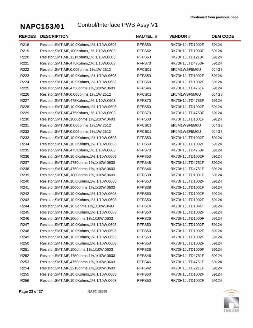
Continued from previous page
NAPC153/01 Control/Interface PWB Assy,V1
REFDES NAUTEL #DESCRIPTION VENDOR # OEM CODE
R218 RFFS50Resistor,SMT,MF,10.0Kohms,1%,1/10W,0603 RK73H1JLTD1002F 59124
R219 RFFS62Resistor,SMT,MF,100Kohms,1%,1/10W,0603 RK73H1JLTD1003F 59124
R220 RFFS63Resistor,SMT,MF,121Kohms,1%,1/10W,0603 RK73H1JLTD1213F 59124 R221 RFFS70Resistor,SMT,MF,475Kohms,1%,1/10W,0603 RK73H1JLTD4753F 59124
R222 RFCS01Resistor,SMT,MF,0.005ohms,1%,1W,2512 ERJM1WSF5M0U 0J4G8
R223 RFFS50Resistor,SMT,MF,10.0Kohms,1%,1/10W,0603 RK73H1JLTD1002F 59124 R224 RFFS50Resistor,SMT,MF,10.0Kohms,1%,1/10W,0603 RK73H1JLTD1002F 59124
R225 RFFS46Resistor,SMT,MF,4750ohms,1%,1/10W,0603 RK73H1JLTD4751F 59124
R226 RFCS01Resistor,SMT,MF,0.005ohms,1%,1W,2512 ERJM1WSF5M0U 0J4G8 R227 RFFS70Resistor,SMT,MF,475Kohms,1%,1/10W,0603 RK73H1JLTD4753F 59124
R228 RFFS50Resistor,SMT,MF,10.0Kohms,1%,1/10W,0603 RK73H1JLTD1002F 59124 R229 RFFS70Resistor,SMT,MF,475Kohms,1%,1/10W,0603 RK73H1JLTD4753F 59124
R230 RFFS38Resistor,SMT,MF,1000ohms,1%,1/10W,0603 RK73H1JLTD1001F 59124
R231 RFCS01Resistor,SMT,MF,0.005ohms,1%,1W,2512 ERJM1WSF5M0U 0J4G8 R232 RFCS01Resistor,SMT,MF,0.005ohms,1%,1W,2512 ERJM1WSF5M0U 0J4G8
R233 RFFS50Resistor,SMT,MF,10.0Kohms,1%,1/10W,0603 RK73H1JLTD1002F 59124
R234 RFFS50Resistor,SMT,MF,10.0Kohms,1%,1/10W,0603 RK73H1JLTD1002F 59124 R235 RFFS70Resistor,SMT,MF,475Kohms,1%,1/10W,0603 RK73H1JLTD4753F 59124
R236 RFFS50Resistor,SMT,MF,10.0Kohms,1%,1/10W,0603 RK73H1JLTD1002F 59124
R237 RFFS46Resistor,SMT,MF,4750ohms,1%,1/10W,0603 RK73H1JLTD4751F 59124 R238 RFFS46Resistor,SMT,MF,4750ohms,1%,1/10W,0603 RK73H1JLTD4751F 59124
R239 RFFS38Resistor,SMT,MF,1000ohms,1%,1/10W,0603 RK73H1JLTD1001F 59124
R240 RFFS50Resistor,SMT,MF,10.0Kohms,1%,1/10W,0603 RK73H1JLTD1002F 59124 R241 RFFS38Resistor,SMT,MF,1000ohms,1%,1/10W,0603 RK73H1JLTD1001F 59124
R242 RFFS50Resistor,SMT,MF,10.0Kohms,1%,1/10W,0603 RK73H1JLTD1002F 59124 R243 RFFS50Resistor,SMT,MF,10.0Kohms,1%,1/10W,0603 RK73H1JLTD1002F 59124
R244 RFFS14Resistor,SMT,MF,10.0ohms,1%,1/10W,0603 RK73H1JLTD10R0F 59124
R245 RFFS50Resistor,SMT,MF,10.0Kohms,1%,1/10W,0603 RK73H1JLTD1002F 59124 R246 RFFS26Resistor,SMT,MF,100ohms,1%,1/10W,0603 RK73H1JLTD1000F 59124
R247 RFFS50Resistor,SMT,MF,10.0Kohms,1%,1/10W,0603 RK73H1JLTD1002F 59124
R248 RFFS50Resistor,SMT,MF,10.0Kohms,1%,1/10W,0603 RK73H1JLTD1002F 59124 R249 RFFS50Resistor,SMT,MF,10.0Kohms,1%,1/10W,0603 RK73H1JLTD1002F 59124
R250 RFFS50Resistor,SMT,MF,10.0Kohms,1%,1/10W,0603 RK73H1JLTD1002F 59124
R251 RFFS26Resistor,SMT,MF,100ohms,1%,1/10W,0603 RK73H1JLTD1000F 59124 R252 RFFS46Resistor,SMT,MF,4750ohms,1%,1/10W,0603 RK73H1JLTD4751F 59124
R253 RFFS46Resistor,SMT,MF,4750ohms,1%,1/10W,0603 RK73H1JLTD4751F 59124
R254 RFFS42Resistor,SMT,MF,2210ohms,1%,1/10W,0603 RK73H1JLTD2211F 59124 R255 RFFS50Resistor,SMT,MF,10.0Kohms,1%,1/10W,0603 RK73H1JLTD1002F 59124
R256 RFFS50Resistor,SMT,MF,10.0Kohms,1%,1/10W,0603 RK73H1JLTD1002F 59124
Page 23 of 27 NAPC153/01
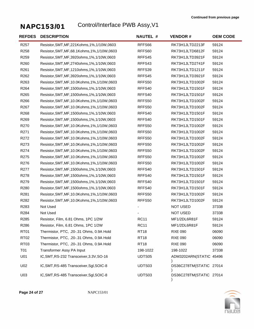
Continued from previous page
NAPC153/01 Control/Interface PWB Assy,V1
REFDES NAUTEL #DESCRIPTION VENDOR # OEM CODE
R257 RFFS66Resistor,SMT,MF,221Kohms,1%,1/10W,0603 RK73H1JLTD2213F 59124
R258 RFFS60Resistor,SMT,MF,68.1Kohms,1%,1/10W,0603 RK73H1JLTD6812F 59124
R259 RFFS45Resistor,SMT,MF,3920ohms,1%,1/10W,0603 RK73H1JLTD3921F 59124 R260 RFFS43Resistor,SMT,MF,2740ohms,1%,1/10W,0603 RK73H1JLTD2741F 59124
R261 RFFS39Resistor,SMT,MF,1210ohms,1%,1/10W,0603 RK73H1JLTD1211F 59124
R262 RFFS45Resistor,SMT,MF,3920ohms,1%,1/10W,0603 RK73H1JLTD3921F 59124 R263 RFFS50Resistor,SMT,MF,10.0Kohms,1%,1/10W,0603 RK73H1JLTD1002F 59124
R264 RFFS40Resistor,SMT,MF,1500ohms,1%,1/10W,0603 RK73H1JLTD1501F 59124
R265 RFFS40Resistor,SMT,MF,1500ohms,1%,1/10W,0603 RK73H1JLTD1501F 59124 R266 RFFS50Resistor,SMT,MF,10.0Kohms,1%,1/10W,0603 RK73H1JLTD1002F 59124
R267 RFFS50Resistor,SMT,MF,10.0Kohms,1%,1/10W,0603 RK73H1JLTD1002F 59124 R268 RFFS40Resistor,SMT,MF,1500ohms,1%,1/10W,0603 RK73H1JLTD1501F 59124
R269 RFFS40Resistor,SMT,MF,1500ohms,1%,1/10W,0603 RK73H1JLTD1501F 59124
R270 RFFS50Resistor,SMT,MF,10.0Kohms,1%,1/10W,0603 RK73H1JLTD1002F 59124 R271 RFFS50Resistor,SMT,MF,10.0Kohms,1%,1/10W,0603 RK73H1JLTD1002F 59124
R272 RFFS50Resistor,SMT,MF,10.0Kohms,1%,1/10W,0603 RK73H1JLTD1002F 59124
R273 RFFS50Resistor,SMT,MF,10.0Kohms,1%,1/10W,0603 RK73H1JLTD1002F 59124 R274 RFFS50Resistor,SMT,MF,10.0Kohms,1%,1/10W,0603 RK73H1JLTD1002F 59124
R275 RFFS50Resistor,SMT,MF,10.0Kohms,1%,1/10W,0603 RK73H1JLTD1002F 59124
R276 RFFS50Resistor,SMT,MF,10.0Kohms,1%,1/10W,0603 RK73H1JLTD1002F 59124 R277 RFFS40Resistor,SMT,MF,1500ohms,1%,1/10W,0603 RK73H1JLTD1501F 59124
R278 RFFS40Resistor,SMT,MF,1500ohms,1%,1/10W,0603 RK73H1JLTD1501F 59124
R279 RFFS40Resistor,SMT,MF,1500ohms,1%,1/10W,0603 RK73H1JLTD1501F 59124 R280 RFFS40Resistor,SMT,MF,1500ohms,1%,1/10W,0603 RK73H1JLTD1501F 59124
R281 RFFS50Resistor,SMT,MF,10.0Kohms,1%,1/10W,0603 RK73H1JLTD1002F 59124 R282 RFFS50Resistor,SMT,MF,10.0Kohms,1%,1/10W,0603 RK73H1JLTD1002F 59124
R283 -Not Used NOT USED 37338
R284 -Not Used NOT USED 37338 R285 RC11Resistor, Film, 6.81 Ohms, 1PC 1/2W MF1/2DL6R81F 59124
R286 RC11Resistor, Film, 6.81 Ohms, 1PC 1/2W MF1/2DL6R81F 59124
RT01 RT18Thermistor, PTC, .20-.31 Ohms, 0.9A Hold RXE 090 06090 RT02 RT18Thermistor, PTC, .20-.31 Ohms, 0.9A Hold RXE 090 06090
RT03 RT18Thermistor, PTC, .20-.31 Ohms, 0.9A Hold RXE 090 06090
T01 198-1022Transformer Assy PA Input 198-1022 37338 U01 UDTS05IC,SMT,RS-232 Transceiver,3.3V,SO-16 ADM3202ARN(STATIC
) 45496
U02 UDTS03IC,SMT,RS-485 Transceiver,Sgl,SOIC-8 DS36C278TM(STATIC)
27014
U03 UDTS03IC,SMT,RS-485 Transceiver,Sgl,SOIC-8 DS36C278TM(STATIC)
27014
Page 24 of 27 NAPC153/01

Continued from previous page
NAPC153/01 Control/Interface PWB Assy,V1
REFDES NAUTEL #DESCRIPTION VENDOR # OEM CODE
U04 UDLS07IC,SMT,CMOS,Quad Nand Schmitt,SOIC-14 SN74HC132D(STATIC)
01295
U05 UDAS01IC,SMT,Trans Array, 7 Darl.,SOIC-16 MC1413BD(STATIC)(ROHS) ON SEMI
04713
U06 UDAS01IC,SMT,Trans Array, 7 Darl.,SOIC-16 MC1413BD(STATIC)(ROHS) ON SEMI
04713
U07 UDTS05IC,SMT,RS-232 Transceiver,3.3V,SO-16 ADM3202ARN(STATIC)
45496
U08 UDLS05IC,SMT,CMOS,8-Bit Shft Reg,Par O/P, SOIC-16 MC74HC595AD(STATIC)
04713
U09 ULAS01IC,SMT,Opamp,Quad,Single Supply,SOIC-14 MC33074AD(STATIC) 04713 U10 UD68IC,SMT,Optocoupler,High CMR &Speed Gull Wing 6N137-
300E(STATIC)(ROHS) AVAGO TECHNOLOGIES
AVAGO
U11 UD68IC,SMT,Optocoupler,High CMR &Speed Gull Wing 6N137-300E(STATIC)(ROHS) AVAGO TECHNOLOGIES
AVAGO
U12 UDAS01IC,SMT,Trans Array, 7 Darl.,SOIC-16 MC1413BD(STATIC)(ROHS) ON SEMI
04713
U13 UDLS05IC,SMT,CMOS,8-Bit Shft Reg,Par O/P, SOIC-16 MC74HC595AD(STATIC)
04713
U14 UMDS01IC,SMT,DAC,8-Bit,4-ch,SPI,SOIC-14 TLV5620ID(STATIC) 64155
U15 UT73IC,DC-DC Converter,3kV ISO,5V-5V,1W NMV0505SA(STATIC) C&D
U16 ULAS02IC,SMT,Opamp,Quad,Rail-To-Rail,SOIC-14 TLV2374ID(STATIC) 01295 U17 ULAS01IC,SMT,Opamp,Quad,Single Supply,SOIC-14 MC33074AD(STATIC) 04713
U18 UDLS07IC,SMT,CMOS,Quad Nand Schmitt,SOIC-14 SN74HC132D(STATIC)
01295
U19 UMAS01IC,SMT,ADC,10-Bit,11-ch,SPI,SOIC-20 TLC1543IDW(STATIC)
01295
U20 UMDS01IC,SMT,DAC,8-Bit,4-ch,SPI,SOIC-14 TLV5620ID(STATIC) 64155 U21 UDOS01IC,SMT,Dual Optocoupler,SOIC-8 MOCD223-M(STATIC) 7D893
U22 UDOS01IC,SMT,Dual Optocoupler,SOIC-8 MOCD223-M(STATIC) 7D893
U23 UG35IC,CMOS,Hex Schmitt,Trigger Inverter,SOIC-14 MM74HC14M(STATIC)
07263
U24 UDAS01IC,SMT,Trans Array, 7 Darl.,SOIC-16 MC1413BD(STATIC)(ROHS) ON SEMI
04713
U25 ULAS02IC,SMT,Opamp,Quad,Rail-To-Rail,SOIC-14 TLV2374ID(STATIC) 01295 U26 UG35IC,CMOS,Hex Schmitt,Trigger Inverter,SOIC-14 MM74HC14M(STATIC)
07263
U27 UX83IC,SMT,2.5V Reference,0.1%,SOT-23-6 LT1790BIS6-2.5(STATIC)
64155
U28 UDLS01IC,SMT,CMOS,Octal Flip Flop,SOIC-20 SN74AHC574DW(STATIC)
01295
U29 UDOS01IC,SMT,Dual Optocoupler,SOIC-8 MOCD223-M(STATIC) 7D893 U30 UDOS01IC,SMT,Dual Optocoupler,SOIC-8 MOCD223-M(STATIC) 7D893
U31 -Not Used NOT USED 37338
U32 UDOS01IC,SMT,Dual Optocoupler,SOIC-8 MOCD223-M(STATIC) 7D893
Page 25 of 27 NAPC153/01

Continued from previous page
NAPC153/01 Control/Interface PWB Assy,V1
REFDES NAUTEL #DESCRIPTION VENDOR # OEM CODE
U33 UDOS01IC,SMT,Dual Optocoupler,SOIC-8 MOCD223-M(STATIC) 7D893
U34 ULAS02IC,SMT,Opamp,Quad,Rail-To-Rail,SOIC-14 TLV2374ID(STATIC) 01295
U35 ULAS02IC,SMT,Opamp,Quad,Rail-To-Rail,SOIC-14 TLV2374ID(STATIC) 01295 U36 ULAS02IC,SMT,Opamp,Quad,Rail-To-Rail,SOIC-14 TLV2374ID(STATIC) 01295
U37 ULCS01IC,SMT,Comparator,Quad,SOIC-14 MC3302D(STATIC) 04713
U38 UDPS01IC,SMT,Complex Program LogicDev, PLCC-84 XC9572-15PC84C(STATIC)
68994
U39 UMAS01IC,SMT,ADC,10-Bit,11-ch,SPI,SOIC-20 TLC1543IDW(STATIC)
01295
U40 UMAS01IC,SMT,ADC,10-Bit,11-ch,SPI,SOIC-20 TLC1543IDW(STATIC)
01295
U41 ULAS02IC,SMT,Opamp,Quad,Rail-To-Rail,SOIC-14 TLV2374ID(STATIC) 01295
U42 UT74IC, Amplifier, Instrumentation MAX4080SASA(STATIC)
1E566
U43 ULRS02IC,SMT,4.096V Reference,0.1%,SOT-23-6 LT1790BIS6-4.096(STATIC)
64155
U44 UDMS02IC, SMT, Micro, ADC, PWM,Flash, TQFP-64 ATMEGA128-16AI(STATIC)
1FN41
U45 UDLS01IC,SMT,CMOS,Octal Flip Flop,SOIC-20 SN74AHC574DW(STATIC)
01295
U46 UT74IC, Amplifier, Instrumentation MAX4080SASA(STATIC)
1E566
U47 UT74IC, Amplifier, Instrumentation MAX4080SASA(STATIC)
1E566
U48 UT74IC, Amplifier, Instrumentation MAX4080SASA(STATIC)
1E566
U49 UDLS02IC, SMT, CMOS, Octal Latch,SOIC-20 SN74AHC573DW(STATIC)
01295
U50 UDLS01IC,SMT,CMOS,Octal Flip Flop,SOIC-20 SN74AHC574DW(STATIC)
01295
U51 UDMS01IC, SMT, SRAM, 32Kx8, SOIC-28(Wide) CY62256LL-70SNI(STATIC)
65786
U52 UT74IC, Amplifier, Instrumentation MAX4080SASA(STATIC)
1E566
U53 UDSS01IC,SMT,Non-Volatile RAM Ctrlr,SOIC-8 DS1312S-2(STATIC) 0B0A9 U54 UG35IC,CMOS,Hex Schmitt,Trigger Inverter,SOIC-14 MM74HC14M(STATIC)
07263
U55 UDTS01IC,SMT,Real-Time Clock,SPI,SOIC-16 M41T94MQ6(STATIC) U3040
U56 ULAS01IC,SMT,Opamp,Quad,Single Supply,SOIC-14 MC33074AD(STATIC) 04713 U57 ULAS01IC,SMT,Opamp,Quad,Single Supply,SOIC-14 MC33074AD(STATIC) 04713
U58 UDAS01IC,SMT,Trans Array, 7 Darl.,SOIC-16 MC1413BD(STATIC)(ROHS) ON SEMI
04713
U59 UDAS01IC,SMT,Trans Array, 7 Darl.,SOIC-16 MC1413BD(STATIC)(ROHS) ON SEMI
04713
U60 UMDS01IC,SMT,DAC,8-Bit,4-ch,SPI,SOIC-14 TLV5620ID(STATIC) 64155 XBT01 BBHT01Holder, 20mm Coin Cell, PWB Mt 1065 91833
XE01 JQ16Conn, Header, SIP,12 Pin Breakawy,.10 Ctr 1-103185-2 09482
XE02 JQ16Conn, Header, SIP,12 Pin Breakawy,.10 Ctr 1-103185-2 09482
Page 26 of 27 NAPC153/01

Continued from previous page
NAPC153/01 Control/Interface PWB Assy,V1
REFDES NAUTEL #DESCRIPTION VENDOR # OEM CODE
Y01 XFPS01Crystal,SMT,Fund,Par Res,11.0592MHz CMR309T11.0592MABJTR
3DX59
Y02 XFPS02Crystal,SMT,Fund,Par Res,32.768kHz MC20632.7680KA-A0 1JRT7
NARF49/01 Final Assy, V1 (RLS 2)
REFDES NAUTEL #DESCRIPTION VENDOR # OEM CODE
A01 NAPC153/01Control/Interface PWB Assy,V1 204-2070-01 37338
A03 NAPA16APA PWB Assy, HD 198-1030-02 37338 A04 NAPA16APA PWB Assy, HD 198-1030-02 37338
A05 NAPA16APA PWB Assy, HD 198-1030-02 37338
A06 NAPA16APA PWB Assy, HD 198-1030-02 37338 A07 PN85BPWB Detail, Reject Load 204-8429 37338
A08 PN95BPWB Detail, Common Point 204-8493 37338 A09 204-8490-01Power Probe PWB Assy 204-8490-01 37338
A7R1 RAB45Resistor, MF, 47.5K Ohms, 1PC1/4W MF1/4DL4752F 59124
A7R2 RT52Res,(BeO),50 ohms,5%,250W,0.25" tabs,Flng Mt. BEO250B-R12 37338 A7R3 RT52Res,(BeO),50 ohms,5%,250W,0.25" tabs,Flng Mt. BEO250B-R12 37338
A7R4 RT52Res,(BeO),50 ohms,5%,250W,0.25" tabs,Flng Mt. BEO250B-R12 37338
A7R5 RT52Res,(BeO),50 ohms,5%,250W,0.25" tabs,Flng Mt. BEO250B-R12 37338 A7RT1 RX07Thermistor, 200K Ohms @ 25C 135-204QAG-J01 1BH13
B01 204-8407-01Fan Assy, V1 (Dual Blower) 204-8407-01 37338
J02 JDP26Conn, Coax, BNC, Recept, 50ohm UG1094/U 02660 J03 JDP26Conn, Coax, BNC, Recept, 50ohm UG1094/U 02660
L04 198-6102Choke Assy, Lightning Drain 198-6102 37338
RT01 RX07Thermistor, 200K Ohms @ 25C 135-204QAG-J01 1BH13 RT02 RX07Thermistor, 200K Ohms @ 25C 135-204QAG-J01 1BH13
S01 SD63Switch,Rocker,DPST,250Vac/16A JWL21BA2A-A NKK SWITU01 JT80Conn,Recept,AC,250V,20A,Quick-Dis 83030400(RoHS) INTERPOW
U02 UG41Power Supply, AC-DC,85-246Vac,50W, 5,15,24-15 out REL-70-4007(STATIC) INTEGRATED POWER
INTEGRAT
U03 UG39Power Supply,6-53V,208 nom I/P2120W, 50A 011-146501-1 TECTROL
U04 204-2045-01Mod, UDDS01 LCD 204-2045-01 37338 U08 UG52Power Supply, Univ Input, 12V,75W LPS-75-12(Static) MEANWEL
Page 27 of 27 NARF49/01


V1 Repair Manual Page 5-1 Section 5 Wiring Information Issue 2.2
V1 REPAIR MANUAL Section 5 WIRING INFORMATION
5.1 INTRODUCTION This section contains wiring information for hard-wired assemblies of the subject unit. Refer to Table 5-1 for an itemized listing of assemblies that have wiring lists. 5.2 WIRING LISTS NOT PROVIDED Separate wiring lists are not provided for some assemblies, including: • Assemblies that have separate
maintenance manuals. Refer to the associated maintenance manual for detailed wiring information of these assemblies.
• Assemblies that have their wiring
information adequately depicted/ tabulated on their assembly detail drawings. Refer to the associated assembly detail drawing for detailed wiring information of these assemblies.
5.3 PRINTED WIRING PATTERNS Printed wiring pattern information is beyond the scope of this manual. Therefore, detailed printed wiring patterns for printed circuit boards are not included. 5.4 WIRE COLOURS Every effort is made to manufacture the assemblies using wire that is the colour tabulated in the ‘Code’ column of the wiring list tables. In some instances, a white wire will be substituted. In this case identification must be determined by locating the assigned identification number. 5.5 WIRING LIST PROVIDED Wiring lists are provided in table format. A list of the table numbers and the associated wiring list are shown in Table 5-1. These lists provide non-printed wiring pattern, point-to-point (source/destination) inter-connecting information.
Table 5-1: Wiring Lists Provided Table # Description 5-2 Wiring List – V1 Transmitter 5-3 Connector Mating Information – V1 Transmitter
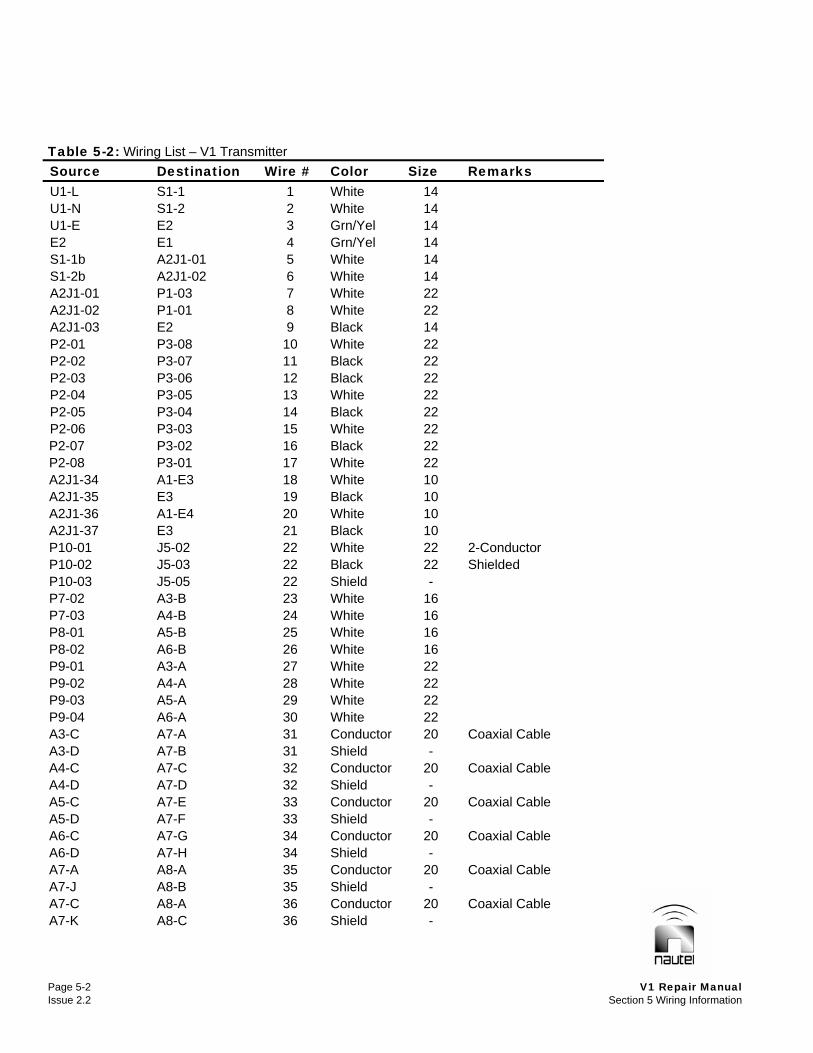
Page 5-2 V1 Repair Manual Issue 2.2 Section 5 Wiring Information
Table 5-2: Wiring List – V1 Transmitter Source Destination Wire # Color Size Remarks U1-L S1-1 1 White 14 U1-N S1-2 2 White 14 U1-E E2 3 Grn/Yel 14 E2 E1 4 Grn/Yel 14 S1-1b A2J1-01 5 White 14 S1-2b A2J1-02 6 White 14 A2J1-01 P1-03 7 White 22 A2J1-02 P1-01 8 White 22 A2J1-03 E2 9 Black 14 P2-01 P3-08 10 White 22 P2-02 P3-07 11 Black 22 P2-03 P3-06 12 Black 22 P2-04 P3-05 13 White 22 P2-05 P3-04 14 Black 22 P2-06 P3-03 15 White 22 P2-07 P3-02 16 Black 22 P2-08 P3-01 17 White 22 A2J1-34 A1-E3 18 White 10 A2J1-35 E3 19 Black 10 A2J1-36 A1-E4 20 White 10 A2J1-37 E3 21 Black 10 P10-01 J5-02 22 White 22 2-Conductor P10-02 J5-03 22 Black 22 Shielded P10-03 J5-05 22 Shield - P7-02 A3-B 23 White 16 P7-03 A4-B 24 White 16 P8-01 A5-B 25 White 16 P8-02 A6-B 26 White 16 P9-01 A3-A 27 White 22 P9-02 A4-A 28 White 22 P9-03 A5-A 29 White 22 P9-04 A6-A 30 White 22 A3-C A7-A 31 Conductor 20 Coaxial Cable A3-D A7-B 31 Shield - A4-C A7-C 32 Conductor 20 Coaxial Cable A4-D A7-D 32 Shield - A5-C A7-E 33 Conductor 20 Coaxial Cable A5-D A7-F 33 Shield - A6-C A7-G 34 Conductor 20 Coaxial Cable A6-D A7-H 34 Shield - A7-A A8-A 35 Conductor 20 Coaxial Cable A7-J A8-B 35 Shield - A7-C A8-A 36 Conductor 20 Coaxial Cable A7-K A8-C 36 Shield -
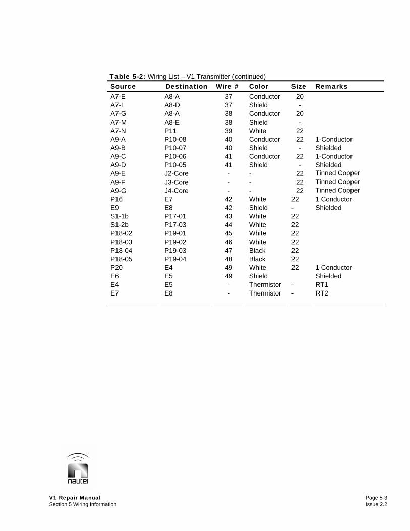
V1 Repair Manual Page 5-3 Section 5 Wiring Information Issue 2.2
Table 5-2: Wiring List – V1 Transmitter (continued) Source Destination Wire # Color Size Remarks A7-E A8-A 37 Conductor 20 A7-L A8-D 37 Shield - A7-G A8-A 38 Conductor 20 A7-M A8-E 38 Shield - A7-N P11 39 White 22 A9-A P10-08 40 Conductor 22 1-Conductor A9-B P10-07 40 Shield - Shielded A9-C P10-06 41 Conductor 22 1-Conductor A9-D P10-05 41 Shield - Shielded A9-E J2-Core - - 22 Tinned Copper A9-F J3-Core - - 22 Tinned Copper A9-G J4-Core - - 22 Tinned Copper P16 E7 42 White 22 1 Conductor E9 E8 42 Shield - Shielded S1-1b P17-01 43 White 22 S1-2b P17-03 44 White 22 P18-02 P19-01 45 White 22 P18-03 P19-02 46 White 22 P18-04 P19-03 47 Black 22 P18-05 P19-04 48 Black 22 P20 E4 49 White 22 1 Conductor E6 E5 49 Shield Shielded E4 E5 - Thermistor - RT1 E7 E8 - Thermistor - RT2

Page 5-4 V1 Repair Manual Issue 2.2 Section 5 Wiring Information
Table 5-3: Connector Mating Information – V1 Transmitter Connector Mate P1 U2P1 P2 U2P2 P3 A1J9 P4 A2J2 P5 A1J8 P6 A1J21 P7 A1J13 P8 A1J14 P9 A1J16 P10 A1J22 P11 A1E5 **P12 A1J11 **P13 **U6-Port 1 **P14 A1J7 **P15 **U6-DC Input P16 A1E7 P17 U8CN1 P18 U8CN2 P19 A1J23 P20 A1E6 U4P1 A1J12 U5P1 A1J10 B1P1 A1J15 W1P1 A1J17 W1P2 A3J1 W2P1 A1J18 W2P2 A4J1 W3P1 A1J19 W3P2 A5J1 W4P1 A1J20 W4P2 A6J1 **W5P1 **U6-Ethernet **W5P2 **U7J2
NOTE ** - Connector or mate applies only when NxLink module is installed.
V1 Repair Manual Page 6-1 Section 6 Electrical Schematics Issue 2.2
V1 REPAIR MANUAL Section 6 ELECTRICAL SCHEMATICS
6.1 INTRODUCTION This section contains electrical schematics/ logic diagrams for the subject equipment. Block diagrams, simplified electrical schematics, and/or logic diagrams may be included. Refer to Table 6-1 for an itemized listing. 6.2 COMPONENT VALUES Unless otherwise specified on the logic/ schematic diagram, the following applies: • Resistor values are shown in ohms.
(K = 1000 and M = 1 000 000). • Resistor power ratings are not shown
when less than 0.5 W. • Capacitor values are shown in
microfarads (uF). • Unidentified diodes are part number
1N4938. 6.3 GRAPHIC SYMBOLS The graphic symbols used on electrical schematics are in accordance with American National Standard ANSI Y32.2-1975 - Graphic Symbols for Electrical and Electronic Diagrams. 6.4 LOGIC SYMBOLS The logic symbols used on electrical schematics and logic diagrams are in accordance with American National Standard ANSI Y32.14-1975 - Graphic Symbols for Logic Diagrams. 6.5 REFERENCE DESIGNATIONS Reference designations were assigned in accordance with American National Standard ANSI Y32.16-1975 - Reference Designations for Electrical and Electronic Parts and Equipment. Each electrical symbol is identified with its basic reference designation. To obtain the full reference designation for a specific part, this basic identifier must be
prefixed with the reference designation assigned to all higher assemblies. 6.6 UNIQUE SYMBOLOGY Nautel utilizes unique symbology on electrical schematics to describe two-state (logic) inputs/outputs that differ from those inputs/ outputs having only one distinct state or multiple states (analog). 6.6.1 Type of Inputs/Outputs On electrical schematics, names used to describe two-state (logic) inputs/outputs are prefixed by a '#'. Those inputs/outputs representing a one-state or analog signal will have no prefix. 6.6.2 Logic Level/Convention The '#' prefix identifies an input/output that has two distinct states - 'high' and 'low'. A suffix, '+' or '-', identifies the active (true) state of the input/output. The 'high' (+) is the more positive of the two levels used to represent the logic states. The 'low' (-) is the less positive of the two levels used to represent the logic states. Two types of logic, positive and negative, may be represented on a particular schematic. In positive logic, 'high' represents the active (true) state and 'low' represents the inactive (false) state. In negative logic, 'low' represents the active state and 'high' represents the inactive state. 6.7 IDENTIFICATION OF SCHEMATIC DIAGRAMS A number that is both the figure number and the page number identifies each illustration in this section. The numbers are assigned sequentially and are prefixed by the letters 'SD-'. The electrical schematics/logic diagrams included in this section are listed in Table 6-1.

Page 6-2 V1 Repair Manual Issue 2.2 Section 6 Electrical Schematics
6.8 STRUCTURE OF SCHEMATICS The electrical schematics are structured in a hierarchical format that is based on function and signal flow. Wherever practical, the signal flow is from left to right. Inputs normally originate on the left-hand side and outputs will extend to the right-hand side. Exceptions are shown by an arrow indicating the direction of signal flow.
NOTE The physical location of a part/assembly was not necessarily a factor when a schematic was drawn. The full reference designation assigned to a part/ assembly, in conjunction with the family tree in Figure 4-1 and the assembly detail drawings in section 7, will identify its location. Figure SD-1 identifies the major stages. Each stage contains cross-references that identify which block is the signal source for inputs or the destination for outputs. When a sub-function is treated as a block, its detailed circuit information is included in its own schematic drawing(s), also included in this section. 6.9 LOCATING THE SCHEMATIC DIAGRAM(S) FOR A FUNCTIONAL BLOCK The text inside a functional block provides the key to locating its schematic diagram(s). When a functional block is assigned a reference designation, refer to the family tree depicted in Figure 4-1 and follow the family tree branches to the block that contains the reference designation and associated Nautel nomenclature (e.g., NAPC153/01). Refer to Table 6-1 with the Nautel nomenclature number and/or the description to identify the appropriate figure number(s).
6.10 LOCATING A PART/ASSEMBLY IDENTIFIED ON A SCHEMATIC The full reference designation assigned to a part/assembly is the key to physically locating that part/assembly.
NOTE Full reference designations contain the assembly hierarchical coding. When the end item is divided into units (cabinets), the first coding is a unit number (1, 2, 3, etc). When the end item is divided into assemblies, the first coding is an assembly number (A1, A2, A3, etc). If a unit or an assembly is divided into sub-assemblies, assembly coding that identifies assembly relationship (1A1, A2A1, A2A1A1, etc) is added. Refer to the family tree depicted in Figure 4-1 with the full reference designation and follow the family tree branches to the appropriate block, noting the name and Nautel nomenclature number of all higher assemblies in the path.
NOTE The drawings in Section 7 depict the assembly detail of the transmitter and its modules/assemblies. Refer to Table 7-1 with the name and Nautel nomenclature number of each family tree block in the path, starting at the highest assembly (normally Figure MD-1) and determine the figure number(s) for that assembly. Refer to the referenced figure and locate the next lower level assembly. Repeat this procedure until the location of the required part/assembly is found.

V1 Repair Manual Page 6-3 Section 6 Electrical Schematics Issue 2.2
Table 6-1: List of Electrical Schematics Figure # Description SD-1 Electrical Schematic – V1 Transmitter
SD-2 Electrical Schematic – Control/Interface PWB (NAPC153/01) (Sheet 1 of 5)
SD-3 Electrical Schematic – Control/Interface PWB (NAPC153/01) (Sheet 2 of 5)
SD-4 Electrical Schematic – Control/Interface PWB (NAPC153/01) (Sheet 3 of 5)
SD-5 Electrical Schematic – Control/Interface PWB (NAPC153/01) (Sheet 4 of 5)
SD-6 Electrical Schematic – Control/Interface PWB (NAPC153/01) (Sheet 5 of 5)
SD-7 Electrical Schematic – Power Amplifier PWB (NAPA16A)
SD-8 Electrical Schematic – Power Probe PWB (204-8490-01)


Dimensions = mm (inches)
Electrical Schematic - V1 - 1,000 Watt FM Broadcast Transmitter Issue 2.2 Not to Scale Figure SD-1 Sheet 1 of 1
RF ON
UP KEY
L
N
P8
P7
U5P1
1J4
J14
J14
J16
J13
J16
J13
J7
J11
J1
J8
J15
RX-
RX+TX-
RXD
J5
+
+
A3
NxLINK
P4
W5P1
J2
J1 J1
R1
GND
RJ45
J1
A8
J1
GND
P17
J1
PWBPROBE
A9
V+
V+
V-
V-
P2
N/A
GND
+12V
GND
GND
+5V
GND
+24V
GND
+15V
-15V
GND
P11
P16
P5
P19
**
6dB
J22
**
6dB
**
3dB
GND
TXD
RXDTXD
GND
GND
GND
U4RT1
RF OFF
U1
2
J10
J16
J16
TX+
GND
TXD
-
-
A6
A5
A4
U6
E1
P4
A7
GND
U7
U3
P1
E8
E5
PA V
A2
U8
U2
RT1
V+
V-
N/A
GND
+12V
P10
P20
P3
PWB
A1
J3
J2
RXD
GND
GND
GND
GND
E2
(FROM EXTERNALRF DRIVE INPUT
J1
OVERLAY
U5
COMB FAN TACH 2COMB FAN TACH 1
COMB FAN VDC
COMB RF DRIVE POWERSYSTEM REFLD POWER
# EXT RF OFF -# EXT RF ON -
# EXT RESET -# EXT EXCITER TOGGLE -
# EXT PRESET 6 -
# EXT PRESET 4 -# EXT PRESET 5 -
# EXT PRESET 1 -
# EXT PRESET 2 -
N/CBIAS CURRENT -
TRANSMITTER INTERLOCK
SOFT KEY 1
SOFT KEY 3
E
P9
1P9
2
3P7
1P9
2P7
2
P14
3
J3
23
3
7
2
1P5
CONTROL/INTERFACE
PART OF7
J14 5
3
B1P11
J22 2
P10
20
18
J1013
3
U5P11
AC POWER
PA 4 VOLTS
PA 3 VOLTS
RF DRIVE (3)
BIAS 2
PA 2 VOLTS
RF DRIVE (2)
BIAS 1
PA 1 VOLTS
RF DRIVE (1)
GND
GND
RXD
TXD
(TO EXCITER XMTR LINK)EXCITER LINK
GND
FAN B TACH
+12V (FAN B)
FAN A TACH
+12V (FAN A)
RS2323
LED COMMON
# REMOTE LED -
# RF ON LED -
# PA LED -
# EXTERNAL LED -
VAC
VAC/N
B CPA PWB
B CPA PWB
A D
PORT 1ETHERNET
FRONT
RF OUTPUT (4)
RF OUTPUT (3)E
RF OUTPUT (2)C
B
RF OUTPUT (1)
E2(-)
10
INH
A2PART OF
GROUND
STATIONREFERENCE
E
C
J
W5P2
# PWR SUPPLY INHIBIT +
PA VOLTS CONTROL -
PA VOLTS CONTROL +
VAC LINE 2
A
A
A
POINTPWB
B
(OPTIONAL)
LAN (RJ45)J2
J1
POWERSUPPLY
F
# MODULE PRESENT -
# AC FAIL +
# PS FAIL -
# SUPPLY TEMP -
PA VOLTS -
PA VOLTS +
H
N/C
J2
J1PS INTERFACE
1
AC/N CN1CN2
SUPPLY+12V POWER
6
LOW VOLTAGE
P1
RF MONITOR
RF SAMPLEE
REFLD PWRC
FWD PWR
REJECT LOAD TEMP
INTAKE TEMP
# AC FAIL +
# PS FAIL -
# SUPPLY TEMP -P4
E3PA VOLTS -
PA VOLTS +
P18
ATTENUATOR ATTENUATOR
E5
E6
J8
E4
1
J23
J12
J9
INTERFACECONTROL/
PART OF
ATTENUATOR J2
REMOTE ANALOG SAMPLE 5
# MASTER OK STATUS OUT -
REMOTE ANALOG SAMPLE 3
REMOTE ANALOG SAMPLE 2REMOTE ANALOG SAMPLE 1
+24V (REMOTE)
# RF ON STATUS -# EXCITER B STATUS -
# PRESET 5 STATUS -# PRESET 6 STATUS -
# PRESET 3 STATUS -# PRESET 2 STATUS -# PRESET 1 STATUS -
# LOW RF ALARM -
# PA FAIL ALARM -# REMOTE STATUS -# INTERLOCK OPEN ALARM -
EXCITER INTERLOCK
FS
LCD TEMP
D5D6
D3D4
D0D1
9LED ARESET
RD
CE 7
VEEWR
4
VSS 2
FGND
(LCD)
U4
SOURCE)
FRONTPANEL
PART OF
S2040145 V3
COMB BUS VDC
COMB REJ TEMP
SYSTEM FWD POWER
# EXT PRESET 3 -
N/C
DOWN KEY
SOFT KEY 2
2
4
P8
3
P9
P8
1
5
2P12
PWB
1
6
J13
2
A1
6
8
4
21
19
3
1
14
4
2
1 1b
2 2b
S1
RF DRIVE (4)
BIAS 4
BIAS 3
P13
+15V (NX LINK)
B1-A
B1-B
SHIELD
# LOCAL LED -
2
5
# RF OFF LED -
# OUTPUT NETWORK LED -
# POWER SUPPLY LED -
B CPA PWB
A D
A D
A D
B CPA PWB
(OPTIONAL)
GNDE2
PANEL
PART OFU5
G
H
D
F
A
9
J2E1(+)
PS INTERFACE PWB
G
M
50250W
R5
K
L50250W
R4
A
P
R250250W
50250W
R3
47.5K
VAC LINE 1
E
C
D
A
COMMON
COUPLER
MODULEPA VOLTS SAMPLE
PA VOLTS -
PA VOLTS +
N/C
POWER
RT2
FAIL
TEMP
PWB
PART OF
FG
AC/L
POWER SUPPLY
RF OUTPUT
F
A
B
EXHAUST TEMP
PA VOLTS -
PA VOLTS +
P2
(OPTIONAL) (OPTIONAL)
E7
E3 2
J4
(OPTIONAL)
SERIAL BUS (SLAVE)
J3
# COMB FAN ENABLE +
REMOTE ANALOG SAMPLE 4
+15V (REMOTE)
# PRESET 4 STATUS -
# SUMMARY ALARM -
# HIGH TEMP ALARM -
(TO EXCTR INTLK CIRCUIT)
D7
D2
C/D
VCC
6
8
5
3
U4P1
DISPLAYGRAPHIC
P
N
RT1
1
J19 W3P1 J1W3P2
COMB REJECT LOAD POWER B19
B11B10
B6
B4B3
3
A37
A35A34
# EXT POWER INCREASE - A32
PA VOLTS CONTROL -
# PWR SUPPLY INHIBIT +A29A30
PA VOLTS CONTROL +A27
# FAN B CONTROL -EXTERNAL SUPPLY (+5V TO +30V) A25
3
# FAN A CONTROL -
(9-PIN D-SUB)J21P6
POWER DECREASE 17
SWITCH COMMON 15
11
9
7
5
(180V-264VAC)
10283 28
11227 22
16272 27
15211 21
332 2 2
37
36
ATTENUATORS ARE PART OF ATTENUATOR KIT #198-5350.
B35
6 B33
7 B31B30
B21
B15B13
B9
B1
A23
A20
A21
A18
10
A16A15
10A13
8811
4416
A11A10
6615A8
5533 A6
A5
3737 A3
3636A1
19
20
117
2
3 1415
3 4
12
910
27
187
45
3645
63
542
83 1
71 2
SYSTEM)(TO ANTENNA
RF SAMPLEEXCITER
19
17
14
12
J20 W4P1 J1W4P2
# MASTER OK STATUS IN - B16
J1W2P2J18 W2P1
5
2
B7
B5
B2
DC INPUTP15
# EXT POWER DECREASE -
A36
A31
A33
A28
BIAS CURRENT + 1
(FROM EXTERNAL INTERLOCK)
A26
16POWER INCREASE
12
SERIAL COM
10
8SWITCH COMMON
6
OVERLAY
(47-63Hz)
AC INPUT
REJECT LOAD PWB
(TO/FROM EXTERNAL LAN)
3 3 3
1 1 129
35
34
G
IS USED WITH FM+HD OR HD SYSTEMS.
5DB34
8
B32
B29
B17
B12
E7
E9
E6
E4
A22
A19
A24
B8
9
A12
A14
A9
A17
29
3535
3434
A2
A4
A7
4
2
18
16
135
31
5
11
8
6
3
1
RF OUTPUT
RF MONITOR
16
20
18
15
13
10
W1P2 J1J17 W1P1
11
** DENOTES ATTENUATORS ARE ONLY USED WHEN M50 EXCITER
SERIAL BUS (EXT NxLINK)
# EXCITER RELAY CONTROL/SERIAL SELECT-
# POWER SUPPLY FAIL ALARM -
# BATTERY/MEM FAIL ALARM -# HIGH REFLECTED POWER ALARM -
(FROM EXTERNAL SOURCE)
LOW PASS FILTER

Dimensions = mm (inches)
Electrical Schematic – NAPC153/01 Control/Interface PWB Issue 2.2 Not to Scale Figure SD-2 Sheet 1 of 5
+5V +5V +5V +5V +5V
PF.7
PF.5
INT1
PB.7
PB.6
PF.0
PF.1
PF.2
PE.5
PE.2
PE.3
PE.4
INT0
T1
28
32
30
3
14
13
11
18
8
15
A936
39
38
41
34
43
51
50
48
45
46
D1
D3
D5
D7
+5V
A1
A3
A5
A7
A14
SCK +5V
4DI
3
4N/C
5
6
7VE
20CE
22OE
24A2
23A1
26 A4
2A6
3A7
5A9
7A11
8A12
10A14
1
5GND
100R11
100R12
TX-
RX+
RXD
GND
TXD
GND
RXD
TP26
TP29
PF.6
PF.4
INT7
19
29
10
12
A835
58
33
37
40
42
44
47
49
TP47
D0
D2
D4
D6
4 5
RTC
9 10
A0
A2
A4
A6
A0
1000R28
1N/C
2
0.1C8
27 WE
21A0
28 VCC
4A8
6A10
1A5
25A3
9A13
0.01C6
1RO
0.1C5
221R5
681R6
+5V
1
1
CR7
1
1
1
TX+
RX-
TXD
CR42
TP32
C47
0.1
+5V
681R3
FROM SHEET 2
FROM SHEET 2
FROM SHEET 2
MOSI 4 J6
SWITCH COMMON 15 J10
FROM SHEET 3
RF OFF
RF ON
12 J10
POWER INCREASE
POWER DECREASE 17 J10
DOWN KEY
UP KEY
10 J10
SOFTKEY3
SOFTKEY2
5 J10
SOFTKEY1 7 J10
FROM SHEET 2
FROM SHEET 2
FROM SHEET 4
#CS_RTC-
+5V +5V +5V
#EOC-
+5V +5V
+5V
54
55
56
57
18pFC207
RXD127
RXD02
26
17
61
59
4
6
9
31
64 AVCC
0.01C229
0.1C232
21VCC
TXD1
PD.4
PD.7
PD.5
53GND
TXD0
PB.4
MISO
MOSI
PG.3
PF.3
PE.6
62AREF
PB.5
A10A9
A12
A11A11
A14
A15A14
RD
WR
ALE
AD1
AD3
AD4
AD6
0.1C35
+5V
D0D1
D3
D5D6
8VSS
11SQW
14FT/OUT
#REMOTE_COMMON+
MOSI
#RESET-
TP34
TP33
A15
#WR-
# COMB FAN ENABLE +
TO SHEET 3
TO SHEETS 4 & 5
TO SHEETS 3 , 4 & 5
PROG_RESET
MISO
+5V
TX_NXRX_NX
+5V
#CS_SRAM- 5CEI
8VCCI
7DO/RI
5GND
+5V
1.0C15
0.01C16
5
7 VE6N137-300
U10
3
2
4N/C
7BW
0.1C249
0.01C2503
TOL
6CEO
A1
A4
A6
A9
A11
A14
3 DE
8 VCC
1 C1+7
T2OUT
11T1IN
5C2-10 T2IN
4C2+
2V+ 14
T1OUT
1 1
0.01C68
0.1C42
14GND
RAM
11I/O0
D213I/O2
D417
I/O516
I/O4
D719I/O7
7T2OUT
10T2IN
15GND
13R1IN
R37121K
R38121K
DATATO SHEET 2
2J1
SERIAL BUS(EXCITER LINK)
3J1
RXD(EXT NxLINK)
GNDB32J3
TXDB30J3
(INT NxLINK)5J11
2J11
RXD(SLAVE)
GNDB35J3
TXDB33J3
(RS-232)SERIAL BUS
TO SHEET 2
SWITCH COMMON 8 J10
16 J10
11 J10
9 J10
6 J10
FROM SHEETS 4 & 5
+5V
10.0KR274
10.0KR275
#INT0-
10.0KR224
+5V
BAT54HT1CR33
10.0KR214
10.0KR270
10.0KR271
10.0KR272
10.0KR273
C2090.001
TP28TP31
11.0592MHzY1
10.0KR223
23XTAL2
24XTAL1
16
7
60
10.0KR266
10.0KR282
5
25
0.01C228
0.1C231
52VCC
PG.4
PB.0
63GND
22GND
SCK
20RESET
A8
+5V
DS1G
475R39
1PEN
A13A13
A10
A12
A15
AD0
AD5
AD2
AD7
CPU
+5V
0.01C259
0.1C260
15E
D2
D7
D4
1XI
2XO
6RSTIN2
M41T94MQ6U55
0.1C234
7 10
U58:G
#OE-
MISO
SCK
+5V
0.01C242
#RD-
ALE
TO SHEET 2
TO SHEET 2
PROG_GND
PROG_VCC
0.01C251BT1
3V
TO SHEET 2
TO SHEET 2
0.01C7
0.1C9
31
2U4:A
RX_232_INT
0.1C71
1.0C75
TX_232
RX_232
+5V
2VBAT
RAM MONITOR
0.1C254
0.01C255
2RE
6DO/RI
DS36C278TMU2
+5V
1
1.0C67
0.1C72
1
6
8VCC
4GND
1 N/C 8VCC
A0
1VCCO
A3
A8
A2
A7
A5
A10
A13A12
2 RE
4 DI
DS36C278TMU3
3C1-
6V-
9 R2OUT
8R2IN
12 R1OUT
15GND
0.01C43
0.1C4410
C69
35V 1.0C76
13R1IN
16VCC
ADM3202ARNU1
0.1C41
D1D0
D315I/O3
12I/O1
CY62256LLU51
D6D5
18I/O6
RX_485_INT
221R4
CR2CR1
CR4 CR3
9R2OUT
14T1OUT
8R2IN
#LOW_BAT-
0.1C39
4750R238
6V-
1
R35121K
R36121K
TO SHEET 2
6J1
1J1
SERIAL BUS
SERIAL BUS
B31J3
3J11
SERIAL BUSB34J3
CR43
BAT54HT1CR30
CR38CR39CR40CR41
TP46
4750R225
+5V
CR36
0.1C205
0.01C208
TP27
10.0KR236 R33
681
6N137-300U11
ADM3202ARNU7
18pFC206
RX_INTERNAL
RXD_EXTERNAL
#RF_OFF-
ATmega128-16AIU44
FAN_TACH_MPLX
+5V
+5V
+5V
B12J3
5J69SDO
Y232.768kHz
3J6
5 RSTIN1
16 VCC
4WDI
7 VBAT
CPU OK
+5V
3 D1 18Q1U49:B
5D3
16Q3U49:D
7D5
14Q5U49:F
9D7
12Q7U49:H
1 RO
8VCC
6DO/RI
0.1C3
0.1C17
SHEET 216
VCC
12R1OUT
5C2-
11T1IN
VBAT
+5V
3J22
2J22
S2040143 SHEET 1 OF 5 V2
TP30
CR24 THROUGH CR32 ARE BAT54HT1
10.0KR234
10.0KR267
10.0KR276
+5V
B15J3
TXD_EXTERNAL
1J6
10 SCL12 SDI
R2411000
2J6
6J6
3RST
13 THS
0.01C237
4 D2 17Q2U49:C
2 D0 19Q0U49:A
6D4
15Q4U49:E
8D6
13Q6U49:G
7DO/RI3DE
0.1C4
C2
0.1
TO/FROM
0.1C52
R18
681
4 C2+
2V+
TP48
10.0KR281
3 C1-
1C1+
1J22
CR8
CR37CR44
14 VCC 7GNDU4:ESN74HC132AD
6 11
U58:F
20VCC
10GND1
11 LATCHENABLE
OUTPUTENABLE
U49:ISN74AHC573DW
10.0KR233
R2391000
10.0KR240
1VIN
2 GND
7+V
50VMAU202
U15
1000R32
DS1312S-2U53
# MASTER OK STATUS OUT -
CR1 THROUGH CR4, CR7 & CR8 ARE SMBJ15CA (15V)

Dimensions = mm (inches)
Electrical Schematic – NAPC153/01 Control/Interface PWB Issue 2.2 Not to Scale Figure SD-3 Sheet 2 of 5
TCK
TDI
0.1C182
D0
D2
D5
D7
+5V
D0
D2
D4
D6
D0
D2
D4
D6
VSS
CE
FS
WR
C/D
D0
D2
D3
D5
D7
D2
D4
D6
D0
D2
D4
D6
+5V
E2:3
E2:1
L33
L13
N/O
N/C
TO
A0
+5V
+5V
+5V
+5V
+5V
+5V
+5V
+5V
+5V
+5V
+5V +5V
TMS
TDO
+5V
0.1C176
+5V +5V
D1
D3D4
D6
D1
D3
D5
D7
C2960.01
D1
D3
D5
D7
VCC
RD
VEE
11
11
D4
D1
D6
D1
D3
D5
D0
D7
D1
D3
D5
D7
L34
E2:2
5
+5V +5V +5V +5V +5V
0.1C194
FROM
# PWR SUPPLY FAIL - 6 J8
# AC FAIL + 4 J8
FROM SHEET 4
# SPARE INPUT 4 -
B27 J3# EXCITER B STATUS -
COMB FAN TACH 1
FAN TACH (V1-B)
FAN TACH (V1-A)
TCK 2 J5
TDIJTAG
4 J5
+5V 1 J5
FROMSHEET 4
FROM
S2040143 SHEET 2 OF 5 V2
10.0KR108
10.0KR109
C1230.001
C1240.001
RX_232_INT
RX_NX
A14
#WR-
#RESET-
VO_LCD
10.0KR124
10.0KR125
10.0KR129
C1150.001
C1160.001
C1260.001
10.0KR143
10.0KR145
10.0KR154
32
33
82
35
84
15
10.0KR157
10.0KR158
10.0KR159
13
11 10
U54:E 11
5
65
3 4
U23:B 12
30
29
28
59
+5V
+5V
52
55
31
50
43
47
63
69
61
+5V
21
23
66
+5V
44
83
1
19
51
17
58
68
40
7
0.01C183
73VCC_INT
38VCC_INT
79
75
76
72XC9572-15PC84CU38
70
53
10.0KR196
+5V +5V
+5V +5V +5V
+5V
+5VL40
+5V
10.0KR218
#CS_ADC3-TO SHEET 5
#CS_RMT-
TO SHEET 4#CS_ADC2-
#CS_DAC1-
#CS_RTC-
7J8
#CS_OUT2-
#CS_OUT3-
#CS_OUT1-
FAN_TACH_MPLX
TX_232 TO SHEET 1
RXD_EXTERNAL
TO SHEET 3#RESET_LCD-
RESET10J12
11J12
13J12
15J12
17J12
LED_A9J12
FGND1J12
19J12
5J12
8J12
FROM SHEET 1
+5V
0.1C122
0.1C210
0.01C218
+15V
6 11
U59:F
0.001C18
0.001C19
0.001C83
L32B20J3
# SPARE -L31
B24J3
B22J3
# SPARE -B36J3
INTERLOCKEXCITER
SHEET 4
SERIAL SELECT -B13J3
B29J3
3J15
+12V (FAN A)
+12V (FAN B)5J15
SHIELD
# LOCAL LED -
# REMOTE LED -18J10
# RF ON LED -
# RF OFF LED -14J10
1J10
# PA LED -3J10
LED COMMON20J10
SHEET 3
3 J8
# PWR SUPPLY TEMP - 5 J8
B16 J3
COMB FAN TACH 2
B26 J3
B28 J3
B11 J3
# RF ON STATUS -
GND 6 J5
B10 J3
2 J15
6 J15
TMS
TDO
3 J5
5 J5
SHEET 1
FROM SHEET 3
+5V+5V
4750R252
2210R254
10.0KR101
10.0KR102
+5V
RX_232
RX_485_INT
A15
ALE
#RD-
+5V
10.0KR75
4750R253
10.0KR73
10.0KR74
10.0KR104
+5V +5V +5V
41
81
+5V +5V +5V
80
14
5 6
U54:C
3
10
1 2
U23:A
5 6
U23:C
1 2
U26:A 25
6
34
9 8
U26:D
5 6
U26:C 20
24
18
0.01C196
0.1C197
26
39
57
48
46
45
62
56
9
4
36
2
78VCC_INT
0.01C177
77
74
71
54
CPLD
TP45
67
37
10.0KR203
10.0KR216
10.0KR174
10.0KR263
10.0KR107
+5VL41
L44
TP24
+5VL58
#PA_INHIBIT-
#CS_DAC3-
#CS_ADC1-
8J8
TO SHEET 1#CS_SRAM-
#CS_DAC2- TO SHEET 3
TX_NX
RX_INTERNAL
#INT0-
14J12
12J12
0.5W6.81R285
18J12
16J12
7J12
2J12
3J12
4J12
6J12
0.1C140
+5V
#OE-
13
13
0.01C138
0.1C141
4 13
U24:D
2 15
U24:B
0.01C247
0.1C248
1 16
U58:A
3 14
U58:C
3 14
U59:C
1SMB5939B39V
CR21
0.001C80
0.001C82
0.001C84
10 87
K1:B
3 56K1:A
CR9
+12V
0.001C238
Q2IRF540N
1500
R264
1500
R265
1500
R2681500
R269
1500
R279
1500
R280
# SPARE -
# SPARE -
L14
L30
B25J3
B23J3
B37J3
1J2
2J2
B14J3 # RF ON STATUS -
1J15
7J15
19J10
13J10
2J10
21J10
TO SHEET 1
4J10
C2760.001
C2780.001
C1170.001
C2770.001
3 4
U26:B
0.1C169
0.01C170
0.01C195
0.5W6.81R286
0.1C252
6 11
U24:F
5 12
U59:E
1 16
U59:A
0.0
R19
1SMB5939B39V
CR34
12
1
K1:C
1500
R277
1500
R278
#SPARE1-#RF_ON-
#PWR_DECR-
#PRESET5-#PRESET6-
#PRESET3-
#PRESET1- 10.0KR110
10.0KR111
10.0KR126
60GND
49GND
#INTERLOCK_OPEN-
27GND
C1140.001
C1250.001
+5V10.0KR155
64VCC_IO
+15V
22VCC_IO+5V
#SWR_SHUTBACK+
#LOW_BAT-
#CS_OUT3-
# PWR SUPPLY INHIBIT +
13 12
U54:F
TO LCD
#CS_OUT1-TP25
10.0KR213
TO LCD
+5V
1 16
U24:A2D1
19Q1U28:A
3 14
U24:C4D3
17Q3U28:C
0.001C78
6D5
15Q5U28:E
8D7
13Q7U28:G
#PA2_INHIBIT-4D3
17Q3U45:C
#PA4_INHIBIT-6D5
15Q5U45:E
8D7
13Q7U45:G
+5V
2D1
19Q1U50:A
4D3
17Q3U50:C
6D5
15Q5U50:E
8D7
13Q7U50:G
+15V
DATA
#RMT_RESET-
#PWR_INCR-
#PRESET4-
#PRESET2-
42GND
3 4
U54:B
9 8
U54:D
4750R237
BAT54HT1CR12
8GND
16GND
BAT54HT1CR14
BAT54HT1CR15
10.0KR72
10.0KR103
+12V
TXD_EXTERNAL
10.0KR34
10.0KR217
10.0KR195
#CS_OUT2-
1 2
U54:A
C2950.1
1SMB5939B39V
CR3514
VCC7
GNDU26:GMM74HC14M
9COM
8GNDU59:H
MC1413BD
10GND
20VCC
11CLK
1 OUTPUTENABLE
U28:ISN74AHC574DW
5 12
U24:E
3D2
18Q2U28:B
5D4
16Q4U28:D
7D6
14Q6U28:F
+5V
9D8
12Q8U28:H
10GND
20VCC
11CLK
1 OUTPUTENABLE
U45:ISN74AHC574DW
#PA1_INHIBIT-
#PA3_INHIBIT-
7D6
14Q6U45:F
5D4
16Q4U45:D
3D2
18Q2U45:B
7 10
U59:G
R29182
0.001C221
9D8
12Q8U45:H
R2301000
5D4
16Q4U50:D
7D6
14Q6U50:F
3D2
18Q2U50:B
4 13
U58:D
2 15
U58:B
4 13
U59:D
9D8
12Q8U50:H
C2560.001
BAT54HT1CR13
9 8
U23:D 14VCC
7GNDU23:G
MM74HC14M
7 10
U24:G
14VCC
7GNDU54:G
MM74HC14M
2D1
19Q1U45:A
10GND
20VCC
11CLK
1 OUTPUTENABLE
U50:ISN74AHC574DW
2 15
U59:B
# MASTER OK STATUS IN -
# EXCITER B STATUS -
# EXCITER A ENABLE -
# EXCITER RELAY CONTROL/
# FAN A CONTROL -
# POWER SUPPLY LED -
# EXTERNAL ALARM LED -
# OUTPUT NETWORK LED -
9COM
8GNDU24:H
MC1413BD
# EXCITER B ENABLE -
# FAN B CONTROL -
9COM
8GNDU58:H
MC1413BD

Dimensions = mm (inches)
Electrical Schematic – NAPC153/01 Control/Interface PWB Issue 2.2 Not to Scale Figure SD-4 Sheet 3 of 5
EXT
+5V
3 12 15 6 72 14
12 14
(+)
INT
E1:1
+5V
0.1C61
DAC
R2623920
L23
L20
L22
L21
(-)
L50
A36 J3
A33 J3
A32 J3
A31 J3
A28 J3
A27 J3
A26 J3
0.01C147CR27
0.01C146CR26
0.01C133CR22
0.01C113CR19
+5V
#RF_OFF-
#RMT_RESET-
#PWR_DECR-
#PRESET4-
#PRESET3-
SCK
MOSI
-15V
+15V
+5VL36
#CS_DAC1-
MOSI
+15V
+15V
13
6DATA
8LOAD
14VDD
4REFC
2REFA
5REFD
4REFC
2REFA
1GND
14VDD
6DATA
-15V +5V
-15V +5V
10DACC
1GND
13LDAC
12DACA
11DACB
10DACC
9DACD
10.0KR248
C2710.1
13
R246100
0.001C51
0.001C48
0.001C50
0.001C49
-15V
TO SHEET 2
B17J3
B1J3
B21J3
CONTROL
TO SHEET 4
A37 J3
A35 J3
A34 J3
A29 J3
A30 J3
+15V-AE1:3
E1:2A25 J3
0.01C149CR29
R1382210
0.01C148CR28
R1362210
R1372210
0.01C136CR25
R1352210
0.01C135CR24
R1152210
R1132210
0.01C112CR18
R952210
R962210
0.01C110
0.01C111
CR16
CR17
R932210
R942210
1112
13U4:D 1 16
U5:A
#RF_ON-
#SPARE1-
#PWR_INCR-
#PRESET6-
#PRESET5-
#PRESET2-
#PRESET1-
#CS_DAC2-
#RESET_LCD-
0.1C137
+15V-A
+5V
SCK
3920R259
Q3MMBT4401LT1
2740R260
C1421.035V
7CLK
0.1C287
0.01C290
5REFD
0.001C70
0.1C74
0.1C283
0.001C284 3
REFB
3REFB
0.1C79
0.01C81
TP513
LDAC
8LOAD
7CLK
0.1C151
9DACD
11DACB
12DACA
0.1C286
R24310.0K
10.0KR245
R258
68.1K
1210R261
R24710.0K
0.01C66
R2310.0K
R2410.0K
10.0KR31
0.01C38
10.0KR10
R1510.0K
R1610.0K
0.01C37
0.1C272
0.001C269
R24210.0K
TP37
R25010.0K
R251100
TP35
R2210.0K
R2510.0K
R2710.0
R1410.0K
R1710.0K
R2610.0
0.1C285
B9J3
TO SHEET 4
PA VOLTS
2J8
1J8
A24J3
A22J3
A23J3
A21J3
R1162210
0.01C134CR23
R1142210
10.0KR121
R25510.0K
0.01C264
0.01C65
3
2
1U57:A
10.0KR9
10.0KR30
R24410.0
C2680.01
R2010.0
R2110.0
10.0KR13S2040143 SHEET 3 OF 5 V2
#REMOTE_COMMON+
# EXT RF ON -
TOGGLE -
# EXT PRESET 6 -
# EXT PRESET 5 -
# EXT PRESET 3 -
# EXT PRESET 2 -
# EXT PRESET 1 -
EXTERNAL SUPPLY(+5 TO +30V) REMOTE INPUTS
REMOTE SUPPLY
TO SHEET 1
FROM SHEET 1
FROM SHEET 2
+5V
TO SHEET 2FROM SHEET 4
+5V
+15V
+5V
R257221K
SWR_SHUTBACK_REF
10.0KR249
10.0KR256
REMOTE ANALOG SAMPLE 5
FROM SHEET 1
# EXT RF OFF -
2 15
U5:B
3 6
4 5MOCD223-MU33:B
10.0KR8
3 6
4 5MOCD223-MU32:B
1 8
2 7MOCD223-MU33:A
# EXT EXCITER
# EXT RESET -
3 6
4 5MOCD223-MU30:B
1 8
2 7MOCD223-MU32:A
1 8
2 7MOCD223-MU30:A
# EXT PRESET 4 -
1 8
2 7MOCD223-MU29:A
1 8
2 7MOCD223-MU22:A
1 8
2 7MOCD223-MU21:A
0.1C40
0.1C253
1000R128
DAC REF
FROM SHEET 2
FROM SHEET 1
0.1C261
0.1C155
4VDD
11GNDU34:E
TLV2374ID
4VDD
11GNDU36:E
TLV2374ID
4VCC
11VEEU57:E
MC33074AD
VO_LCD
10
9
8U57:C
C2730.016
5
7U57:B
TLV5620IDU60
10
9
8U9:C
5
6
7U9:B
TLV5620IDU14
DAC_REF
REMOTE ANALOG SAMPLE 4
REMOTE ANALOG SAMPLE 3
REMOTE ANALOG SAMPLE 2
REMOTE ANALOG SAMPLE 1
3 6
4 5MOCD223-MU21:B
3 6
4 5MOCD223-MU22:B
3 6
4 5MOCD223-MU29:B
4VIN
1GND1
2GND2
6VOUT
U27LT1790BIS6-2.5
10
9
8U56:C
3
2
1U9:A
12
13
14U9:D
# EXT POWER DECREASE -
# EXT POWER INCREASE -
4VCC
11VEEU9:E
MC33074AD
4VCC
11VEEU56:E
MC33074AD

Dimensions = mm (inches)
Electrical Schematic – NAPC153/01 Control/Interface PWB Issue 2.2 Not to Scale Figure SD-5 Sheet 4 of 5
MOSI
L38
L37
FWD
+5V
+5V
+5V
+5V
+5V
+5V
+5V
14
L48
L54
MOSI
+5V
Ω1 3
FROM
L39
SCK
PAV
100KR219
R179100
R180100
+5V
GND
1 6 7 8
TO
10 11
GND
13
L49
L51
L53
L55
L56
SCK
3320R45
R44475K
R118.2K
-15V
+5V
L17
2 J19
J17
J18
TP1 TP8 TP2 TP15
L57
L52
121R54
221R55 J20
FROM SHEET 3
REFLECTED POWER
INTAKE TEMP
SHEET 1
EXHAUST TEMP
REJECT LOAD TEMP
BIAS CURRENT -
BIAS CURRENT +
E4
REFLD
0.001C62
3320R164
INTK TEMP
#CS_ADC2-
EXH TEMP
REJ TEMP
0.1C162
+5V
0.1C164
4GND
3N/C
6N/C
5OUT
4GND
6N/C
3N/C
5OUT
4GND
3N/C
6N/C
5OUT
4GND
6N/C
3N/C
5OUT
4GND
6N/C
3N/C
5OUT
1A0
2A1
3A2
17ADDRESS
6A5
CURBIAS
7A6
CUR4
8A7
CUR3
9A8
CUR2
11A9
CUR1
12A10
0.1C109
+15V
+5V
+5V
19EOC
13REF-
14REF+
TO SHEET 2
SHEET 1
FROM SHEET 5
PA4 VOLTS
PA3 VOLTS
PA2 VOLTS
3 J23
+12V 1 J23
-15V 8 J9
-15V
4 J9
6 J9
2 J9
1 J4
#PA4_INHIBIT-
#PA2_INHIBIT-SHEET 2
#CS_DAC3-SHEET 1
DAC_REF
#PA_INHIBIT-
0.1C274
0.01C279
0.1C266
0.01C267
0.1C281
0.01C282
13LDAC
0.01C129
TLV5620IDU20
4REFC
DAC
+15V
0.1C85
A
-15VC361035V
R6339.2K
RF DRV
C
R57100
+12V
-15V
L15
L471J7
+15V
ALARM -A1J3
TO SHEET 2
BIAS 44J16
BIAS 33J16
BIAS 22J16
BIAS 1
TO SHEET 5
FORWARD POWER
FROM SHEET 2
PA VOLTS INE3
0.001C60
TP13
R1602740
12.1KR161
TP14
TP44
10.0KR127
TP10
10.0KR132
TP9
10.0KR130
0.005
R222
2W
0.005
R231
2W
0.005
R232
2W
0.1C159
TP38
R162475K
0.01C217
0.001C224
12.1KR131
0.001C202
0.01C199
0.01C223
0.001C226
0.001C212
0.01C240
0.001C243
R166475K
10.0KR167
R220121K
0.1C168
R151
18.2K
R17310.0K
0.1C154
0.1C145
7N/C
MAX4080SASAU47
7N/C
MAX4080SASAU42
7N/C
7N/C
MAX4080SASAU46
7N/C
MAX4080SASAU52
MAX4080SASAU48
12
13
14U35:DR184100
TP114750R153
R181100
15CS
R182100
18I/O_CLK
4A3
0.1C233
5A4
0.1C200
TP16
100KR197
100KR200
0.1C214
TP18
100KR201
0.1C235
0.1C241
TP19
100KR204
TP20
100KR208
ADC
+5V
0.1C98
0.01C99
0.1C153
0.1C157
GND GND
+5V
BAT54HT1CR31
10.0KR207
0.01C186
10GND
+5V
0.1C184
0.01C185
20VCC
0.1C107
9
GND GND
PA1 VOLTS
4 J23
2 J23
7 J9
+15V
+24V
5 J9
3 J9
+5V 1 J9
#PA3_INHIBIT-
FROM#PA1_INHIBIT-
2 J4
FROM
+5V
RF IN J21
0.1C288
0.01C289
0.01C257
0.1C263
475R46
+5V
1GND
6DATA
7CLK
8LOAD
0.1C119
2REFA
3REFB
5REFD
14VDD
1N5711CR11
C8710pF
+12VTP43
+24VDS4G
TP4
2210R42
+15V
C451016V
TP6
+5V
+5V
C2921035V
2210R40
10.0KR112
10C63
35V
TP3
DS2G
C2931035V
Q12N7002LT1
R88
10.0K
R90
10.0K
R9139.2K
R9722.1K 15.0K
R98
R6122.1K 15.0K
R60
R64
10.0K
R92
10.0K
R5822.1K
0.01C152
TP12
10.0KR146
R185100
RT1RXE090
RT3RXE090
C231035V
10.0KR7
R70100
0.1C100
0.001C101R65
100
0.1C104
0.001C105
0.1C96
0.001C97
0.1C94
0.001C95
R62100
412pFC90
L16A20J3
+24V
L46
L19B8J3
2J7
+15V-A
+5V
1J16
R16315.0K
0.005
R226
2W
R165475K
0.01C213
5
6
7U34:BR183100
TP17
TP23
L42
TP36 TP7
10.0KR120
10.0KR156
B
15.0KR99
R8939.2K
R7139.2K
D
15.0KR59
R10022.1K
0.001C24
RT2RXE090
4 13
U5:D
L18
SWR_SHUTBACK_REF
6 J22
0.001C161
7 J22
E6
E7
E5
8RS-3 J14
1RS+1 J13
8RS-
1RS+
8RS-
1RS+
8RS-
1RS+
8RS-
1RS+
0.1C163
C2701035V
INTERLOCK
MISO
#EOC-
0.1C128
ADC_REFFROM SHEET 2
1J14
3J13
+24V 0.1C33
3320R41
10.0KR118
0.01C32
L5
#INTERLOCK_OPEN-
11DACB
10DACC
9DACD
RF_DRIVE_SAMPLE
0.001C86
Zo = 75
+15V (NX-LINK)
# INTERLOCK OPEN
RF DRIVE (PA #4)
RF DRIVE (PA #1)
0.001C158 12
13
14U34:D
5
4
2U37:A
R1521.21M
5 J22
S2040143 SHEET 4 OF 5 V2
10
9
8U34:C
5
6
7U35:B
47.5KR139
12.1KR147
8 J22
0.1C143
3
2
1U34:A12.1KR133
47.5KR144
0.1C211
0.001C220
0.001C222
2VCC
0.001C201
0.001C203
0.1C204
R221475K
2VCC
0.001C216
0.001C225
0.1C230
0.001C215
R227475K
2VCC
2VCC
0.001C244
0.001C245
0.1C246
R229475K
2VCC
TP22
#SWR_SHUTBACK+
C2911035V
10C258
35V
0.01C108
4VCC
11VEEU17:E
MC33074AD
14VCC
7GND
U18:ESN74HC132AD
C2651035V
4VDD
11GNDU35:E
TLV2374ID
3VCC
12GNDU37:E
MC3302D
C2801016V
16DATA_OUT
TLC1543IDWU39
FROM SHEET 3
0.001C120
2J14
2J13
+12VDS5G
2210R43
DS3G
0.1C262
0.1C34
C641016V
DS6G
10.0KR119
0.1C1
182KR2
12
13
14U17:D
64
5U18:B
10
9
8U17:C
31
2U18:A
12DACA
5
6
7U17:B
89
10U18:C
3
2
1U17:A
3
2
1U35:A
+24V (REMOTE)
+15V (REMOTE)
RF DRIVE (PA #3)
RF DRIVE (PA #2)
R22810.0K
0.1C219
0.001C227
R235475K
3 14
U5:C
10.0KR117
1112
13U18:D
T1

Dimensions = mm (inches)
Electrical Schematic – NAPC153/01 Control/Interface PWB Issue 2.2 Not to Scale Figure SD-6 Sheet 5 of 5
MOSI
+5V
3 5 1 2 876 9
MOSI
SPARE
+5V +5V
L12
L24
L26
L28
A8J3
A6J3
A4J3
A2J3
SCK
-15V
5
ADC
0.1C187
0.01C189
SCK
L1
R69475K
R50475K
0.1C102
0.1C103
0.1C91
0.1C93
L2
L8
L10
L6
A9J3
A5J3
A7J3
A3J3
3320R80
R56475K
#CS_ADC1-
POWERCOMB BUSS VDC
COMB FAN VDC
POWER
POWERSYSTEM FWD
20 J12
S2040143 SHEET 5 OF 5 V2
0.001C192
12.1KR175
0.001C11
0.1C156
0.1C166
+5V
0.1C139
0.1C179
0.1C175
0.1C150
17ADDRESS
15CS
R187100
4A3
6A5
7A6 TLC1543IDW
U40
R192100
9A8
12 A10
+5V
0.1C174
L45
+5V
10
TO SHEET 1
TO SHEET 4ADC_REF
13OE
0.1C73
0.01C77 10
RESET
9SQH
8GND
16VCC
FROM SHEET 2
COMB REJ TEMP B5 J3
B4 J3
B19 J3
B18 J3
FROM SHEET 4
1 16
U6:A7QH
7 10
U12:G5QF
4 13
U12:D3QD
2 15
U12:B1QB
6QG
4QE
2QC
15QA
SCK
+5V
+5V +5V
0.001C28
0.001C29
0.001C30
+5V +5V +5V
0.001C22
0.001C25
0.001C26
L11
L9
L7
L4
18I/O_CLK
4A3
3A2
1A0
TLC1543IDWU19
6A5
8A7
9A8
12 A10
A18J3
A16J3
A14J3
A12J3
A10J3
# REMOTE STATUS -
+5V
TO SHEET 1
RF_DRIVE_SAMPLE
SYSTEM REFLD
+24VR14147.5K
+15VR169100K
+12V
27.4KR209
R210100K
0.001C12
0.001C193
R1762740
R211100K
3320R177
R17815.0K
5
6
7U36:B
12
13
14U36:D
12
13
14U25:D
1SMB5939B39V
CR10
12
13
14U41:D
R205475K
0.1C173
0.1C180 10
9
8U41:C
R198475K
R206475K
5
6
7U41:B
R199475K
0.1C16510
9
8U35:C
0.1C167
R1484750
22.1KR171
18I/O_CLK
R186100
1 A0
2 A1
3A2
R189100
5 A4
R190100
R191100
R193100
R194100
8 A7
11A9
R202100
+5V
0.1C132
BAT54HT1CR32
0.1C198
0.01C188
L43
C1911.035V
10.0KR215
ADC REF
FROM SHEET 1
FROM SHEET 2
#EOC-
MISO
16VCC
14A
8 GND
9 SQH
13OE
14A
#CS_RMT-
FROM SHEET 1
0.1C46
0.01C59 10 RESET
15QA
2QC
6QG
4QE
7 10
U5:G
5 12
U6:E
3 14
U6:C
3QD
5QF
7QH
MOSI
7 10
U6:G1QB
10.0KR66
0.001C106
TP41
R851000
10.0KR86
10.0KR87
0.001C88
0.001C89
TP39
10.0KR47
R48100K
27.4KR52
TP40
0.001C21
0.001C53
0.001C54
12
13
14U16:D
10
9
8U16:C
3
2
1U16:A
0.001C56
0.001C57
0.001C58
L3
L25
L27
L29
17ADDRESS
15 CS
11A9
2 A1
5A4
7 A6
ADC
A19J3
# RF ON STATUS -
A15J3
A17J3
A11J3
A13J3
# LOW RF ALARM -
# PA FAIL ALARM -
0.1C92
#EOC-
MISO
BAT54HT1CR20
0.01C118
0.1C121
0.01C127 L35
R122100K
27.4KR212
R14010.0K
3
2
1U36:A
10
9
8U36:C
3
2
1U41:A
R1491500
10.0KR168
R188100
TP21
TP42
27.4KR49
10.0KR51
R53100K
5
6
7U16:B
3320R83
3320R84
3320R106
3320R82
FROM SHEET 1
FROM SHEET 2
0.001C178
B6 J3
0.001C172
LCD TEMP
6810R142
1500R150
R17212.1K
1SMB5939B39V
CR5
+5V
13REF-
14REF+
20VCC
MC74HC595ADU13
12 LATCH_CLK
0.001C20
0.001C27
2 15
U6:B11SHIFT_CLK
4 13
U6:D
6 11
U6:F
5 12
U5:E
+5V
R77100
13REF-
14REF+
-15V
+24V
20VCC+12V
+15V
+5V
FROM SHEET 4
B7 J3
0.001C171
0.001C181
B3 J3
B2 J3
27.4KR170
+5V
1SMB5939B39V
CR69
COM8
GNDU6:HMC1413BD
4VDD
11GNDU25:E
TLV2374ID
4VDD
11GNDU41:E
TLV2374ID
16DATA_OUT
19EOC
0.1C190
4VIN
1GND1
2GND2
6VOUT
U43LT1790BIS6-4.096
10GND
0.001C31
0.001C55
6 11
U5:F
1 16
U12:A
3 14
U12:C
6 11
U12:F
11SHIFT_CLK
12LATCH_CLK
MC74HC595ADU8
#CS_ADC3-
12.1KR67
47.5KR68
R79100
0.001C10
R78100
19EOC
16DATA_OUT
0.001C13
0.001C14
R76100
10GND
27.4KR123
9 COM 8GNDU5:HMC1413BD
3320R81
3320R105
# EXCITER B STATUS -
# PRESET 6 STATUS -
# PRESET 4 STATUS -
# PRESET 2 STATUS -
# POWER SUPPLY FAIL ALARM -
# HIGH REFLECTED POWER ALARM -
# HIGH TEMP ALARM -
COMB RF DRIVE POWER
COMB REJECT LOAD POWER
# PRESET 5 STATUS -
# PRESET 3 STATUS -
# PRESET 1 STATUS -9COM
8GNDU12:H
MC1413BD
# SUMMARY ALARM -
# BATTERY/MEM FAIL ALARM -
4VDD
11GND
U16:ETLV2374ID

Dimensions = mm (inches)
Electrical Schematic – Power Amplifier PWB (NAPA16A) Issue 2.2 Not to Scale Figure SD-7 Sheet 1 of 1
BIAS
*
T1
C3
L6
L7
D
C
*
C6100pF
C756pF
C90.01
2W
R520
A
BPA VOLTS
C100.01
NOT USED10μF
NAPA16A/01NAPA16A/02
C110μFNAPA16A
NOT USED10μF
NOT USED1000μF, 75V
C1610μF 1000μF, 75V
2W
R1310
**
J1J1
T3:B
T3:A
C140.001
T4 RF OUTRF DRIVE J1
C16
C215pF
NOT USED
C3*
C1*
C51.0
NAPA16A/03
T2:A
T2:B
NOT USED
C110.1
NOT USED
2W
R1020
Q1:B
47.5KR11
2W
R920
C13470pF
L5
C150.001
Q1:A
L2 L4
2W
R1210
L3L1
J1(PAD) - SOLDER
RF DRIVE CONNECTION
S1980249 VB
R115K
C81.0
C120.01
2W
R820
2W20R4
J1(PAD) - SOLDER
2W20R3
* DENOTES SEE CHART BELOW FOR COMPONENT VALUE
** DENOTES INDUCTANCE FORMED BY LEADS OF R12 & R13

Dimensions = mm (inches)
Electrical Schematic – Power Probe PWB (204-8490-01) Issue 2.2 Not to Scale Figure SD-8 Sheet 1 of 1
CR1 R2
27.4 150R11 R12
150
LOW PASS FILTERRF INPUT FROM
FWD PWR PROBE EXCITER RF SAMPLE
D
H
150R17
0.001C6 R14
100R13100150
R18 R163320
C50.001
R327.4 150
R5 R839.2 22.1
R922.1R7
B
F
E
C
G
A
S2040134 VB
REFLD PWR PROBE
FWD PWR
RF MONITOR
RF MONITOR
RF OUTPUT
CR2
3320R15
REFLD PWR
EXCITER RF SAMPLE
R127.4 150
R6

V1 Repair Manual Page 7-1 Section 7 Mechanical Drawings Issue 2.2
V1 REPAIR MANUAL Section 7 MECHANICAL DRAWINGS
7.1 INTRODUCTION This section contains mechanical drawings for assemblies of the subject equipment. Dimensional drawings may be included. Refer to Table 7-1 for an itemized list. Assembly detail drawings for assemblies/ modules that have separate maintenance manuals are not included. Refer to the appropriate maintenance manual for the assembly detail of these assemblies. 7.2 LOCATING ASSEMBLY DETAIL DRAWINGS Each illustration in this section is identified by a number that is both the figure number and the page number. The numbers are assigned sequentially and are prefixed by the letters 'MD-'. Drawings in this section are listed in Table 7-1.
7.3 CONTENT OF MECHANICAL DRAWINGS Mechanical drawings are illustrations that depict the location of electrical components and show assembly outline detail. Dimensional information is included, where appropriate. When a module/assembly is the subject of its own assembly detail drawing and it is also shown in a higher level assembly, the detail depicted in the higher level assembly may have minor differences from the module/ assembly actually installed. In this case, always refer to the assembly detail drawing of the module/assembly for detailed information.
Table 7-1: List of Mechanical Drawings Figure # Description MD-1 Assembly Detail – V1 FM Broadcast Transmitter – Top View
MD-2 Assembly Detail – V1 FM Broadcast Transmitter – Bottom View
MD-3 Assembly Detail – NAPC153/01 Control/Interface PWB
MD-4 Assembly Detail – PS Interface PWB (204-7650-01)
MD-5 Assembly Detail – NAPA16A Power Amplifier PWB
MD-6 Assembly Detail – Power Probe PWB (204-8490-01)


Dimensions = mm (inches)
Assembly Detail – V1 FM Broadcast Transmitter (top cover on) Issue 2.2 Not to Scale Figure MD-1 Sheet 1 of 1
SHOWING REMOVAL OF COOLING FAN B1

Dimensions = mm (inches)
Assembly Detail – V1 FM Broadcast Transmitter – Top View (cover off) Issue 2.2 Not to Scale Figure MD-2 Sheet 1 of 1
U6 DETAIL
PORT 1 (RS-232, D-SUB)
DC INPUT (+15 V, JACK)
ETHERNET I/O (RJ45)

Dimensions = mm (inches)
Assembly Detail – NAPC153/01 Control/Interface PWB Issue 2.2 Not to Scale Figure MD-3 Sheet 1 of 1
R8R7
R20
C81 R69
R120
R224
C263
R254
R24
9C5
C17
C32
1E
2
C47
CR
9R
19
C70
C75
R40
DS
2
DS
3R
41
DS
5
DS
6R
46
C13
2
TP4 TP7
R121
R119TP10
R145
TP12
C15
1
TP13
R16
2
L40
C17
7
TP17 TP18 TP22
R22
2
C21
7
C21
1
C22
9C
228
R23
2
R236
R25
3
R247
C4
RT2 C
76
CR
11
R55
R54
C20
5
C20
8
C1R1
R3
C33
C11C12
L3 C21
L2
C10
L1
L11
L10 C29
C30
L8
L7 C26
C27
L5 C24
C14
C19L13
L14
CR3C35
L18
C15
U3
R11
U2
R27C51L23
R17R16
R25
R15R14
R23R22
L20 C48
C59
C58L29
C46
C56
C55L26
L27
C53L24
C43 R18
R28C52
C80C78
R34
C77
R38
R36
R33
C84
C86
R44
C85
R48 R49R53C89
TP39 TP40R50R51
TP2
C106
R86R85
R68
C102
R84R83
R66
R81R80R79
R77R76
CR14
R75
R73R72
R91R90
R71C99
C107
R89R64R63
C96 C100
C101
R111 CR25
C135
R116R115
R109 CR23
C134
R108
R113C133
R106
C127 C138
C125 CR21
C123
C129
R118
C119
R126 CR29
R138R137C148
R124 CR27
C147
C146R135
R153
C157
R142
R151
C156
R140
C150
R150R149
L39
C152
R128
R133
L38R131
L37
TP45
C170
C169
R177R178
R198R173 R175
C17
3
C167
C166 R192R193R194
R169
R168R188R189R190
C164
R167R186R185
C163R183R182
R161
R165C161R164
R180R179
R213 R218
C196R217
C195
C183
TP23R206C181
C193C192
R205
C179 R209
R203
C190
R202
C189
CR32
C187
C186R207
C184C185
R225
C210 C218
C206
C214
U46
C215
R230
C237
TP29 C242
R233
C241C235
R228
C233
R238
C255L49
C250
C248 C253
R241
C259
R237C256
C252
L46
C274
C282
C281
L54
TP36
C278
C276R258C273
R25
2
R248R256
R260
R25
9
C283
C291
R282R279
CR43
CR40
CR41
C296R271
CR38
L58R268
R264
Q1R2
C3
1
J1
RT1
L15
L16
L4 C22
C20
L9
L6 C25
C28
C31L12
C13
C18
CR
4 L19
C34
C16
C8
C9
C23
1
E1
R26C50L22
L21 C49
R24
C61
R21
C40 U9
C57
U8
L28
C54
C45
C60 C62
C44
L25
C41
K1
R29
C42
C79C74
U14
L31L30
C69
C73
C68R
35
R37
C71
L34
DS
1R
39
R42
DS
4
R45
R43
R47 C88 R52 R87C103
TP41
R82
R78
CR15
R67
R74
R92
CR13
CR12
C104
C105C97R62 R65
R70
C108
R88
C98
R110CR24
R114
U22
C136
C126
U24
L35
CR22
CR20C121
U23
U25
C124
C122
TP6TP3 TP43
TP5
C128
R112
R107
C120 R117
U20
R125
C149
CR28
R136
R129CR26
R15
5
R15
4
R14
3
TP8
R141
R152
C155
R139
TP44 TP9
TP11
R130
C153
C143C145
R127R144R132
C17
6
R19
6
R174
C165
R172R171
R170
R187
R191
R195
C168
C171
R176C172 C
174
TP14 TP15 TP16
C15
8
C159C162
R163
R166 R184
R181
R197R160
TP24
TP25
R214CR30
TP26
L41 R212
C197
C194
L44
R216
C182
R211
TP21
L43
C188
C199
C200
C191
R215C178
C198R210
TP19 TP20
R201 R204 R208
CR31
L42
R219
J18
J17
C209
C207
R22
3
C213C219
C216
C212
R22
6
TP32
C238
TP31TP30
C23
2C
231
C240
R234
CR33
R229C230
R23
1
C254
C247
U53
L48C249
C258
C251
C257
U54
Y2
U55
C26
0
R24
0
R239
R244R242
TP47
RT3
L47C262
C279
C270
U59
C28
0
L56
L55L53
C277
R257R251R250
C271
U57
TP38
TP37TP35TP34
R255
C287
C28
4
C292
R277
R278
R280
CR39
CR44
CR42
C295
R267
R269
R270
R265
CR36
CR37
TP48
C293
R281
U1
L17
R12
U10
E6
C72 U
15
U13
U17
U16
U21
C154
C17
5 C180
C
D
J19
J20
A
U45
U44
U49
E4
U56
1
J7
C261
R243
C27
2
1
J10
R28
6
R31C66C38
R10
C65R30
R9
C83C82
CR10
R32
R5
R6
CR19
C112
R96R95
C111
CR17R56
C110R93
C91
TP42
R105
C90
C141
R102
R103
R104
C117
R101
C114C115
C139
R122
R61 R100
L36
R59R58
R98R97
U27C142
C94
C95
R158
R157
C234
R199
U43
R221R227
U48
U42
R148
C226C202
R146R220
C222
C288
CR35
L52
R275
R276
R273
R274
CR34
R272C264
C269
R266R235
U52 C286
R261
Q3C244 C268
C290
J4
1
C36
C37
L33
U6
C63
CR6
CR5L32
TP1
CR1
CR2
U4
R13
CR7C67
CR8
R4 C6
C2 C7U7
C39
R94
CR18
C113
U30
C93
U28
U19
CR16
C118
C116
U26
C140
R123
C87
R60
R57
R99
U18
C109
C137
R159
U33
C221
TP46R156 Y1
C223
TP27
U36
U37
R147
L45
C204
C227C203
U34
R200
U39
C201 C225
U47
C220 C224
GD
S D
Q2
L57
C289
C267
U50
L51
1
J9
C266
C245
C246
U58
L50
C285
R262
TP33
R246 R263
U60
C243
E7
1
J2
U11
U12
C64U5
J13
1
BT1
E5
U29C92
1
J14
TP28
U32
U35
U41
U40
U38
E3
J16
1
J21
T1
B
U51
C265
J8
1
1
J11
1
J12
R28
5
R2451
J6
J22
1
J23
1
1
J5
J3
T1
J15
1
B C E F H I K L N O Q R T
M3 WASHER
M3 HEX NUT
PWB
1
2
3
4
6
7
8
9
10
A
M2040144 V2
D G J M P S
5
TORQUE ATACHING HARDWARE TO
SEMICONDUCTOR
M3 PAN HEAD SCREW
4.0 INCH POUNDS (0.45 NEWTON METERS)
Q2 MOUNTING DETAIL
#4 BELLEVILLE WASHER
-15V +24V
DAC
+5V INTK EXH CUR4
AD
C
PAV VBAT
GNDGND GND GND
GND
+15V +12V REJ RF DRV FWD BIASGND CUR1CUR2CUR3REFLD
22
33
RE
MO
TE INT
INTE
RLO
CK
EX
CIT
ER
-15V +24V +5V
11
B+
EXT N/CNAPC153
SU
PP
LY N/O
SER.
CONTROL/INTERFACE+12V+15VCPU
44
B+

Dimensions = mm (inches)
Assembly Detail – PS Interface PWB (204-7650-01) Issue 2.2 Not to Scale Figure MD-4 Sheet 1 of 1

Dimensions = mm (inches)
Assembly Detail – NAPA16A Power Amplifier PWB Issue 2.2 Not to Scale Figure MD-5 Sheet 1 of 1

Dimensions = mm (inches)
Assembly Detail – Power Probe PWB (204-8490-01) Issue 2.2 Not to Scale Figure MD-6 Sheet 1 of 1