V Analog Electronics - Miunapachepersonal.miun.se/~amiyou/AE/Lecture5.pdf · Electronic Devices,...
30
© 2012 Pearson Education. Upper Saddle River, NJ, 07458. All rights reserved. Electronic Devices, 9th edition Thomas L. Floyd Analog Electronics – + + V –V Lecture 5
Transcript of V Analog Electronics - Miunapachepersonal.miun.se/~amiyou/AE/Lecture5.pdf · Electronic Devices,...

© 2012 Pearson Education. Upper Saddle River, NJ, 07458.
All rights reserved. Electronic Devices, 9th edition
Thomas L. Floyd
Analog Electronics
–
+
+V
–V
Lecture 5
© 2012 Pearson Education. Upper Saddle River, NJ, 07458.
All rights reserved. Electronic Devices, 9th edition
Thomas L. Floyd
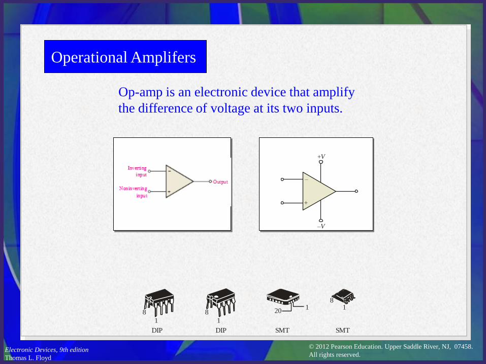
Operational Amplifers
Op-amp is an electronic device that amplify
the difference of voltage at its two inputs.
–
+
+V
–V
120
1
8
DIP
1
8
DIP SMT
18
SMT
© 2012 Pearson Education. Upper Saddle River, NJ, 07458.
All rights reserved. Electronic Devices, 9th edition
Thomas L. Floyd
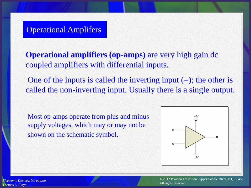
Operational Amplifers
Operational amplifiers (op-amps) are very high gain dc
coupled amplifiers with differential inputs.
One of the inputs is called the inverting input (-); the other is
called the non-inverting input. Usually there is a single output.
Most op-amps operate from plus and minus
supply voltages, which may or may not be
shown on the schematic symbol. –
+
+V
–V
© 2012 Pearson Education. Upper Saddle River, NJ, 07458.
All rights reserved. Electronic Devices, 9th edition
Thomas L. Floyd
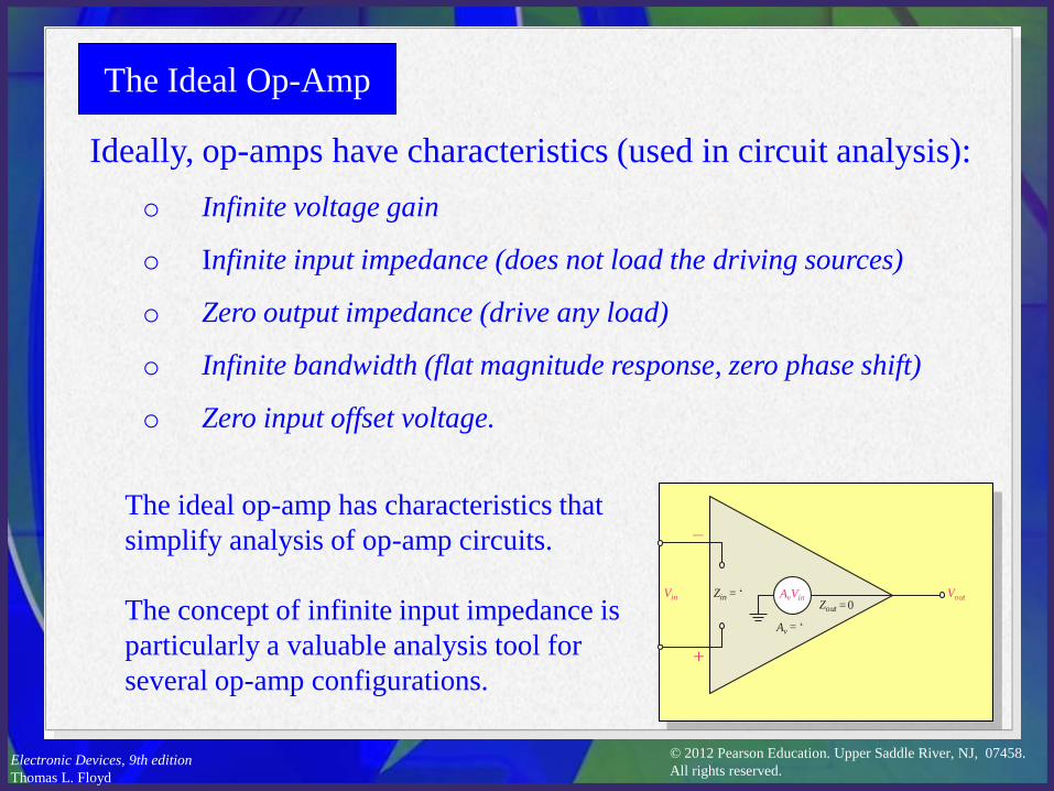
The Ideal Op-Amp
Ideally, op-amps have characteristics (used in circuit analysis):
o Infinite voltage gain
o Infinite input impedance (does not load the driving sources)
o Zero output impedance (drive any load)
o Infinite bandwidth (flat magnitude response, zero phase shift)
o Zero input offset voltage.
–
+
Zin = ‘Vin VoutZout = 0
AvVin
Av = ‘
The ideal op-amp has characteristics that
simplify analysis of op-amp circuits.
The concept of infinite input impedance is
particularly a valuable analysis tool for
several op-amp configurations.
© 2012 Pearson Education. Upper Saddle River, NJ, 07458.
All rights reserved. Electronic Devices, 9th edition
Thomas L. Floyd
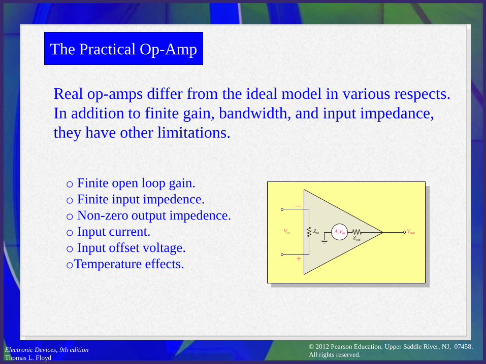
The Practical Op-Amp
Real op-amps differ from the ideal model in various respects.
In addition to finite gain, bandwidth, and input impedance,
they have other limitations.
–
+
ZinVin Vout
Zout
AvVin
o Finite open loop gain.
o Finite input impedence.
o Non-zero output impedence.
o Input current.
o Input offset voltage.
oTemperature effects.
© 2012 Pearson Education. Upper Saddle River, NJ, 07458.
All rights reserved. Electronic Devices, 9th edition
Thomas L. Floyd
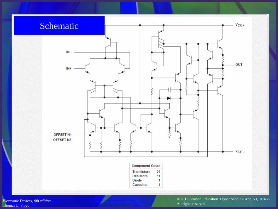
Schematic
© 2012 Pearson Education. Upper Saddle River, NJ, 07458.
All rights reserved. Electronic Devices, 9th edition
Thomas L. Floyd
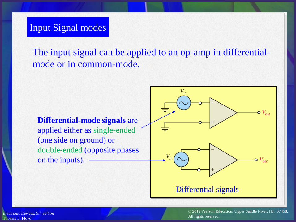
Input Signal modes
The input signal can be applied to an op-amp in differential-
mode or in common-mode.
Differential-mode signals are
applied either as single-ended
(one side on ground) or
double-ended (opposite phases
on the inputs).
Vin
–
+
Vout
Vin
–
+
Vout
Differential signals
© 2012 Pearson Education. Upper Saddle River, NJ, 07458.
All rights reserved. Electronic Devices, 9th edition
Thomas L. Floyd
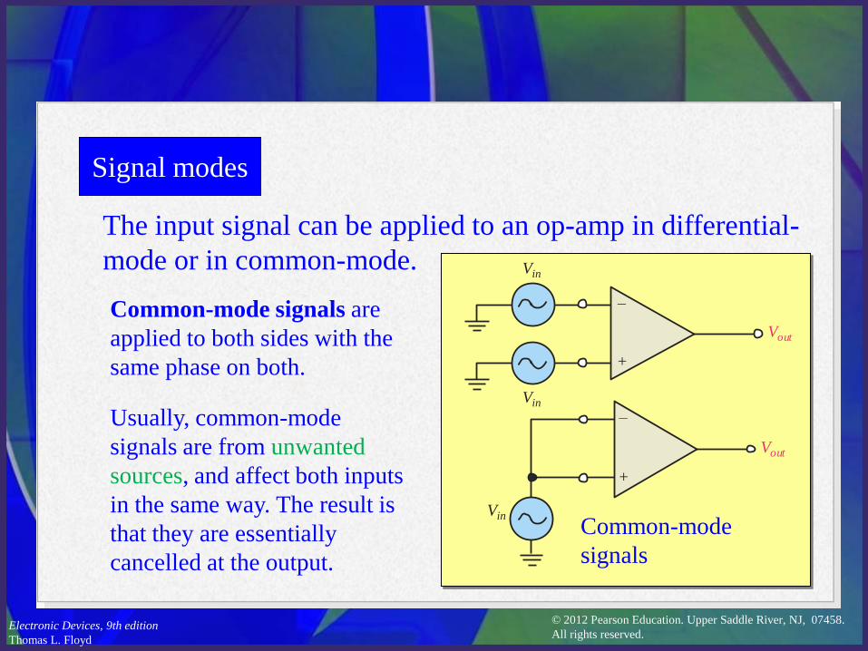
Signal modes
The input signal can be applied to an op-amp in differential-
mode or in common-mode.
Common-mode signals are
applied to both sides with the
same phase on both.
Vin
Vin
–
+
Vout
Vin
–
+
Vout
Usually, common-mode
signals are from unwanted
sources, and affect both inputs
in the same way. The result is
that they are essentially
cancelled at the output.
Common-mode
signals
© 2012 Pearson Education. Upper Saddle River, NJ, 07458.
All rights reserved. Electronic Devices, 9th edition
Thomas L. Floyd
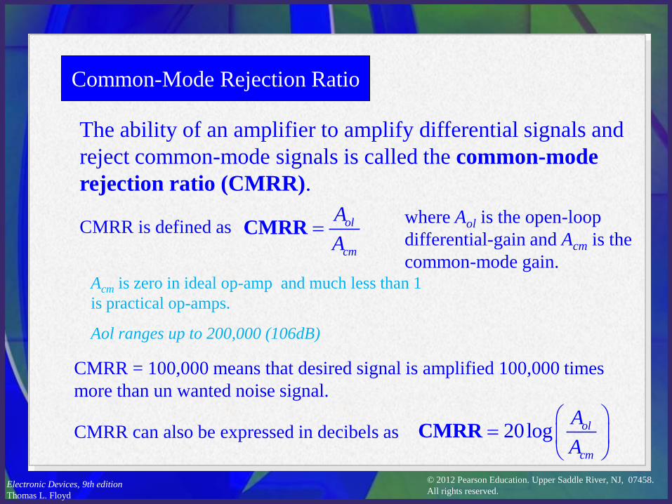
Common-Mode Rejection Ratio
The ability of an amplifier to amplify differential signals and
reject common-mode signals is called the common-mode
rejection ratio (CMRR).
CMRR is defined as ol
cm
A
ACMRR
where Aol is the open-loop
differential-gain and Acm is the
common-mode gain.
CMRR can also be expressed in decibels as 20log ol
cm
A
A
CMRR
Acm is zero in ideal op-amp and much less than 1
is practical op-amps.
Aol ranges up to 200,000 (106dB)
CMRR = 100,000 means that desired signal is amplified 100,000 times
more than un wanted noise signal.
© 2012 Pearson Education. Upper Saddle River, NJ, 07458.
All rights reserved. Electronic Devices, 9th edition
Thomas L. Floyd
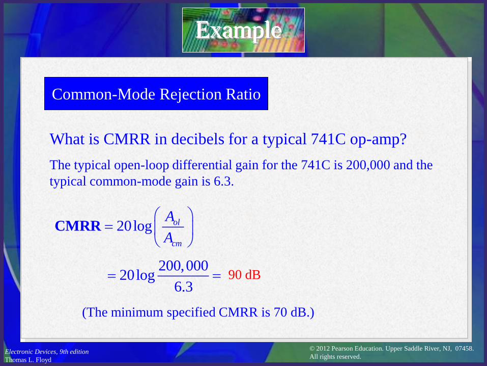
Common-Mode Rejection Ratio
Example
What is CMRR in decibels for a typical 741C op-amp?
The typical open-loop differential gain for the 741C is 200,000 and the
typical common-mode gain is 6.3.
90 dB
20log ol
cm
A
A
CMRR
200,00020log
6.3
(The minimum specified CMRR is 70 dB.)
© 2012 Pearson Education. Upper Saddle River, NJ, 07458.
All rights reserved. Electronic Devices, 9th edition
Thomas L. Floyd
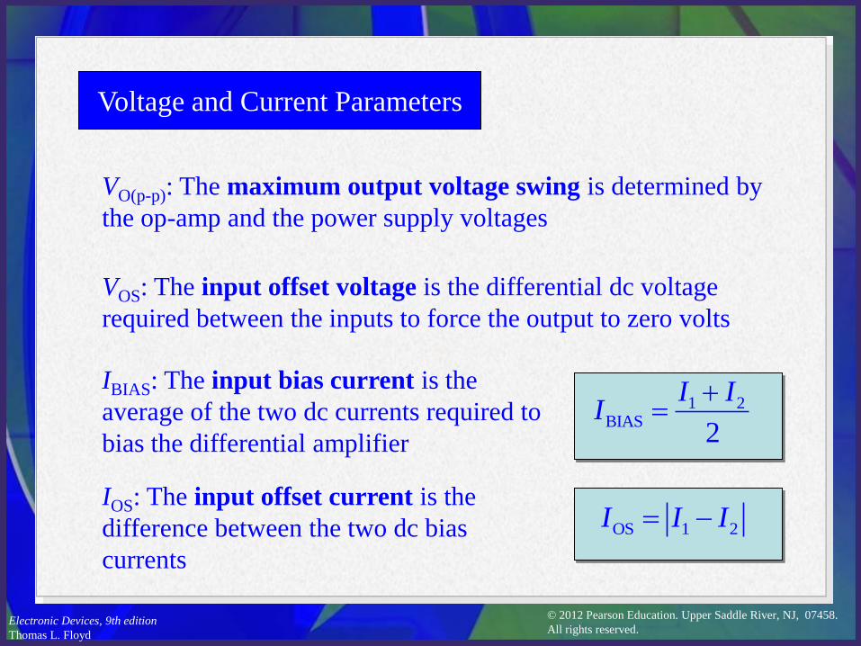
Voltage and Current Parameters
VO(p-p): The maximum output voltage swing is determined by
the op-amp and the power supply voltages
VOS: The input offset voltage is the differential dc voltage
required between the inputs to force the output to zero volts
IBIAS: The input bias current is the
average of the two dc currents required to
bias the differential amplifier
IOS: The input offset current is the
difference between the two dc bias
currents
1 2BIAS
2
I II
OS 1 2I I I -
© 2012 Pearson Education. Upper Saddle River, NJ, 07458.
All rights reserved. Electronic Devices, 9th edition
Thomas L. Floyd
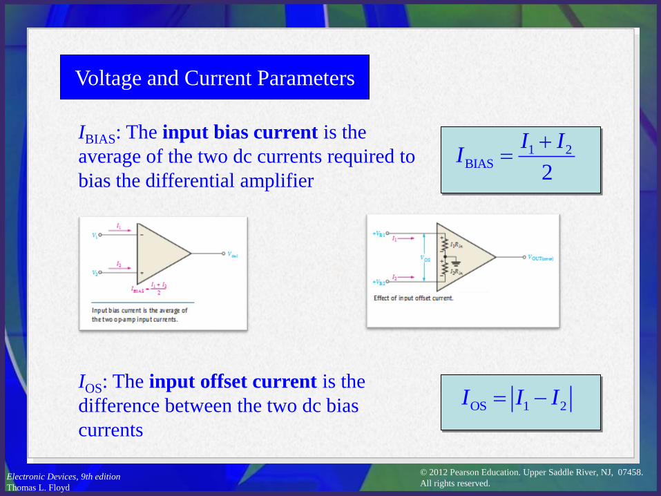
Voltage and Current Parameters
IBIAS: The input bias current is the
average of the two dc currents required to
bias the differential amplifier
IOS: The input offset current is the
difference between the two dc bias
currents
1 2BIAS
2
I II
OS 1 2I I I -
© 2012 Pearson Education. Upper Saddle River, NJ, 07458.
All rights reserved. Electronic Devices, 9th edition
Thomas L. Floyd
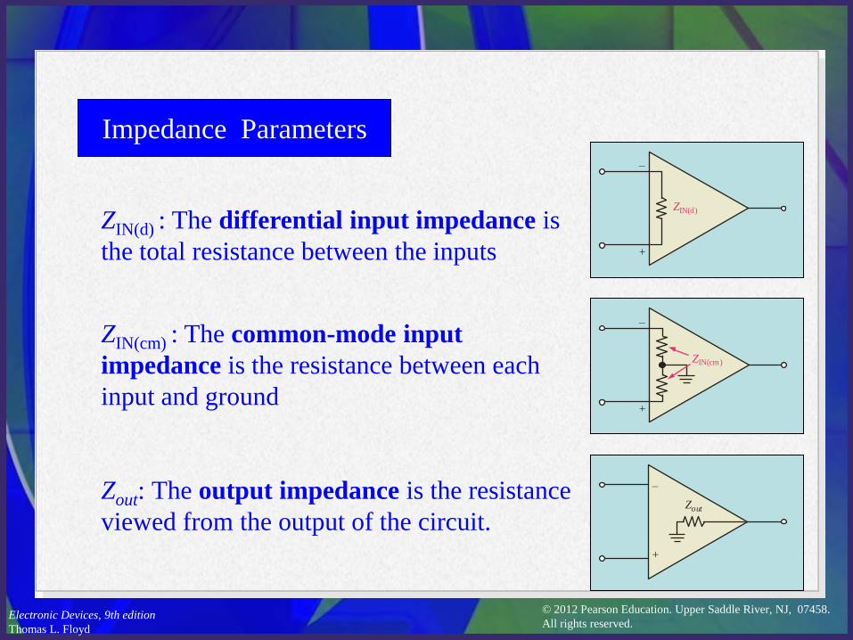
Impedance Parameters
ZIN(d) : The differential input impedance is
the total resistance between the inputs
ZIN(cm) : The common-mode input
impedance is the resistance between each
input and ground
ZIN(d)
–
+
ZIN(cm)
–
+
Zout: The output impedance is the resistance
viewed from the output of the circuit. Zout
–
+
© 2012 Pearson Education. Upper Saddle River, NJ, 07458.
All rights reserved. Electronic Devices, 9th edition
Thomas L. Floyd
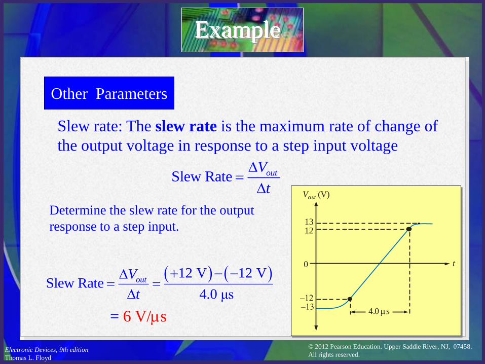
Other Parameters
Example
Slew rate: The slew rate is the maximum rate of change of
the output voltage in response to a step input voltage
Slew Rate outV
t
Determine the slew rate for the output
response to a step input.
12 V 12 VSlew Rate
4.0 μs
outV
t
- -
Vout (V)
t
–13–12
1312
0
4.0 sm= 6 V/ms
© 2012 Pearson Education. Upper Saddle River, NJ, 07458.
All rights reserved. Electronic Devices, 9th edition
Thomas L. Floyd
Negative Feedback
Negative feedback is the process of returning a portion of the
output signal to the input with a phase angle that opposes the
input signal.
Vout
+
–
Vin
Vf
Internal inversion makes Vf
180° out of phase with Vin.
Negativefeedback
circuit
Open loop gain is in order of
100,000.
Even an extremely small input
saturates the out put.
Vin * Aol= (1mv * 100,1000) = 100V
It is not well-controlled
parameter.
One of the most useful concepts in electronics
The advantage of negative feedback is that precise values of amplifier
gain can be set. In addition, bandwidth and input and output impedances
can be controlled.
© 2012 Pearson Education. Upper Saddle River, NJ, 07458.
All rights reserved. Electronic Devices, 9th edition
Thomas L. Floyd
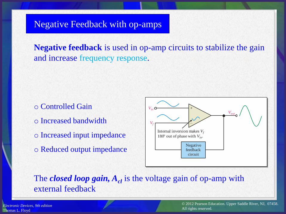
Negative Feedback with op-amps
Negative feedback is used in op-amp circuits to stabilize the gain
and increase frequency response.
Vout
+
–
Vin
Vf
Internal inversion makes Vf
180° out of phase with Vin.
Negativefeedback
circuit
o Controlled Gain
o Increased bandwidth
o Increased input impedance
o Reduced output impedance
The closed loop gain, Acl is the voltage gain of op-amp with
external feedback
© 2012 Pearson Education. Upper Saddle River, NJ, 07458.
All rights reserved. Electronic Devices, 9th edition
Thomas L. Floyd
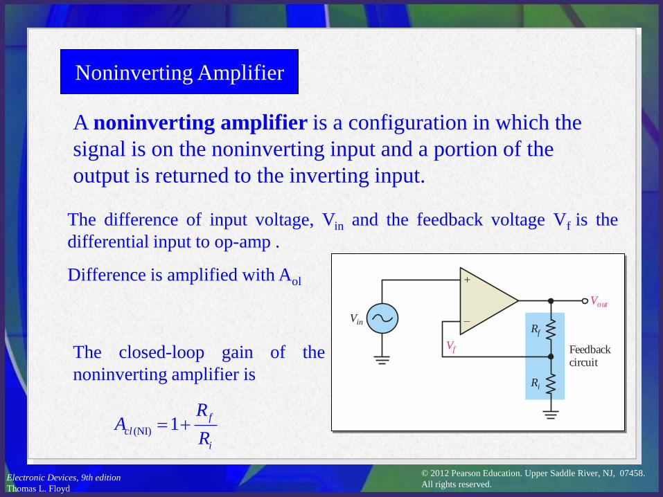
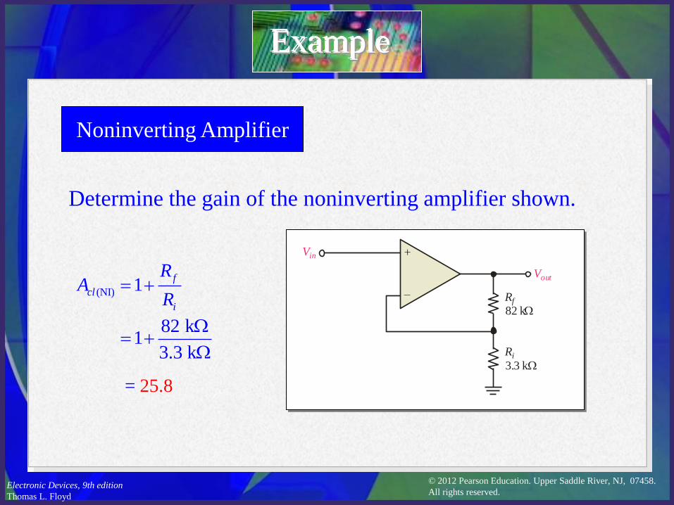
Noninverting Amplifier
A noninverting amplifier is a configuration in which the
signal is on the noninverting input and a portion of the
output is returned to the inverting input.
The closed-loop gain of the
noninverting amplifier is
Rf
Ri
Vf
Vin
+
–
Feedbackcircuit
Vout
(NI) 1f
cl
i
RA
R
The difference of input voltage, Vin and the feedback voltage Vf is the
differential input to op-amp .
Difference is amplified with Aol
© 2012 Pearson Education. Upper Saddle River, NJ, 07458.
All rights reserved. Electronic Devices, 9th edition
Thomas L. Floyd
Noninverting Amplifier
Example
(NI) 1f
cl
i
RA
R
Determine the gain of the noninverting amplifier shown.
Rf
82 kW
Vin +
–
Vout
Ri
3.3 kW
82 k1
3.3 k
W
W
= 25.8
© 2012 Pearson Education. Upper Saddle River, NJ, 07458.
All rights reserved. Electronic Devices, 9th edition
Thomas L. Floyd
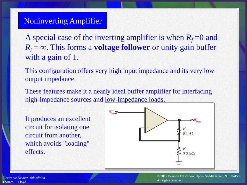
Noninverting Amplifier
A special case of the inverting amplifier is when Rf =0 and
Ri = ∞. This forms a voltage follower or unity gain buffer
with a gain of 1.
Rf
82 kW
Vin +
–
Vout
Ri
3.3 kW
It produces an excellent
circuit for isolating one
circuit from another,
which avoids "loading"
effects.
Vin +
–
Vout
This configuration offers very high input impedance and its very low
output impedance.
These features make it a nearly ideal buffer amplifier for interfacing
high-impedance sources and low-impedance loads.
© 2012 Pearson Education. Upper Saddle River, NJ, 07458.
All rights reserved. Electronic Devices, 9th edition
Thomas L. Floyd
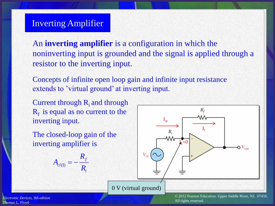
Inverting Amplifier
An inverting amplifier is a configuration in which the
noninverting input is grounded and the signal is applied through a
resistor to the inverting input.
The closed-loop gain of the
inverting amplifier is
(I)
f
cl
i
RA
R -
–
+
Rf
Vout
Ri
Vin
0 V (virtual ground)
Concepts of infinite open loop gain and infinite input resistance
extends to ’virtual ground’ at inverting input.
Current through Ri and through
Rf is equal as no current to the
inverting input.
Iin
If
I1=0
© 2012 Pearson Education. Upper Saddle River, NJ, 07458.
All rights reserved. Electronic Devices, 9th edition
Thomas L. Floyd
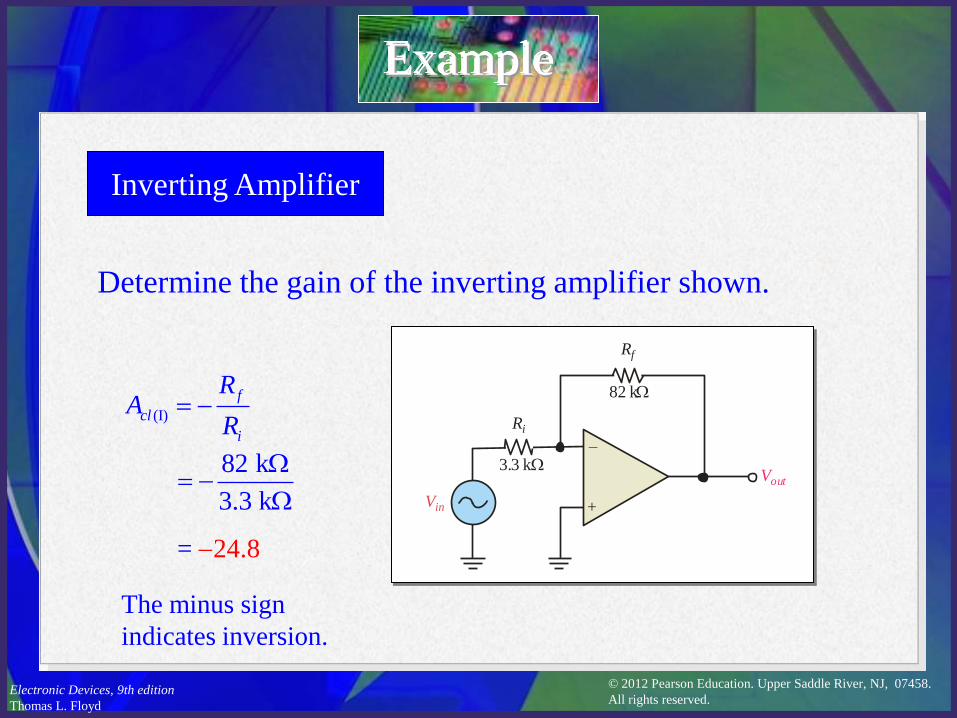
Example
Determine the gain of the inverting amplifier shown.
82 k
3.3 k
W -
W
= -24.8
–
+
Rf
Vout
Ri
Vin
82 kW
3.3 kW
(I)
f
cl
i
RA
R -
The minus sign
indicates inversion.
Inverting Amplifier
© 2012 Pearson Education. Upper Saddle River, NJ, 07458.
All rights reserved. Electronic Devices, 9th edition
Thomas L. Floyd
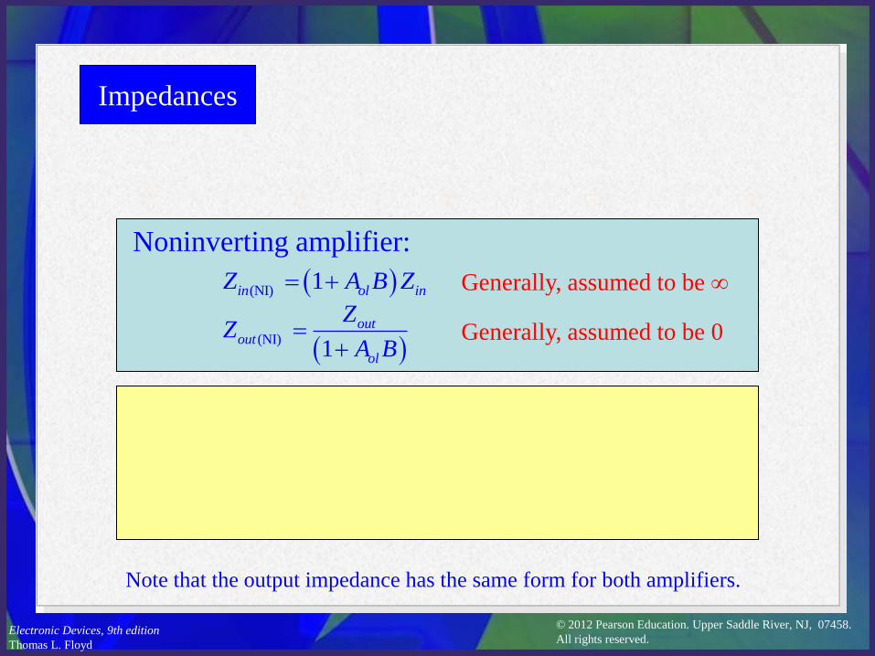
Noninverting amplifier:
Impedances
(NI) 1in ol inZ A B Z
(NI) 1
outout
ol
ZZ
A B
Generally, assumed to be ∞
Generally, assumed to be 0
(I) in iZ R
(I) 1
outout
ol
ZZ
A B
Generally, assumed to be Ri
Generally, assumed to be 0
Inverting amplifier:
Note that the output impedance has the same form for both amplifiers.
© 2012 Pearson Education. Upper Saddle River, NJ, 07458.
All rights reserved. Electronic Devices, 9th edition
Thomas L. Floyd
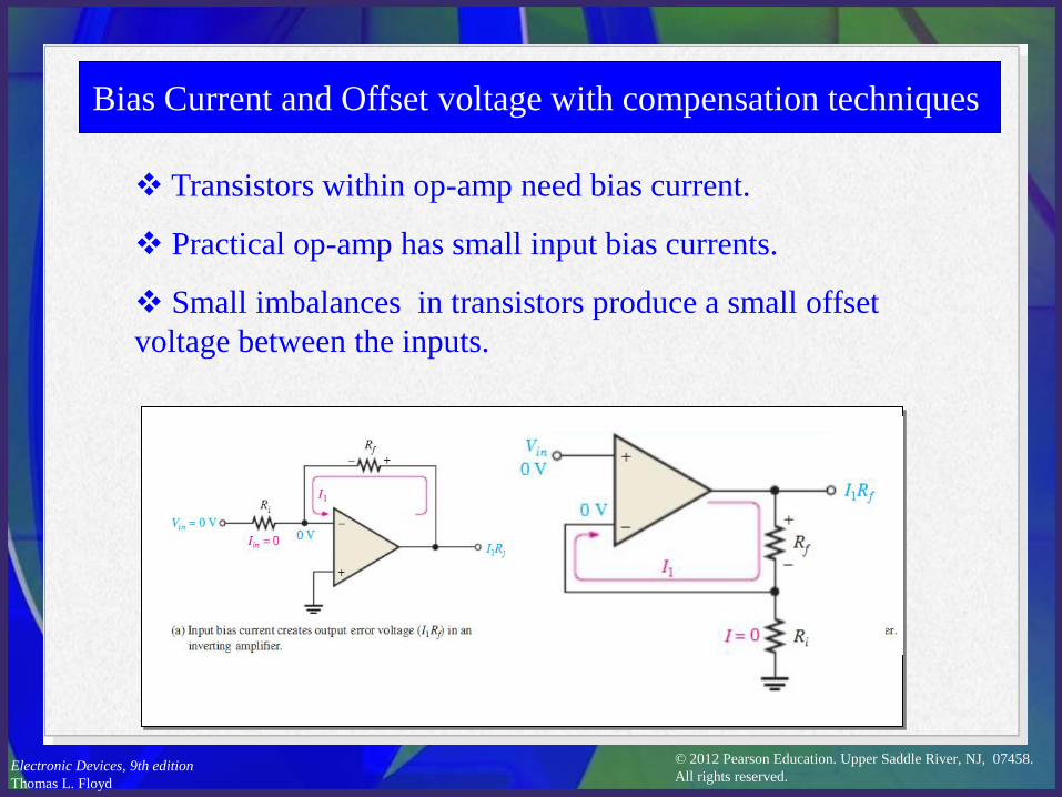
Bias Current and Offset voltage with compensation techniques
Transistors within op-amp need bias current.
Practical op-amp has small input bias currents.
Small imbalances in transistors produce a small offset
voltage between the inputs.
© 2012 Pearson Education. Upper Saddle River, NJ, 07458.
All rights reserved. Electronic Devices, 9th edition
Thomas L. Floyd
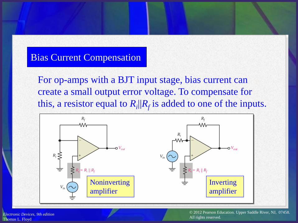
Bias Current Compensation
For op-amps with a BJT input stage, bias current can
create a small output error voltage. To compensate for
this, a resistor equal to Ri||Rf is added to one of the inputs.
–
+
Rf
Vout
Ri
Vin
Rc = Ri || Rf
–
+
Rf
Vout
Ri
Vin
Rc = Ri || Rf
Noninverting
amplifier
Inverting
amplifier
© 2012 Pearson Education. Upper Saddle River, NJ, 07458.
All rights reserved. Electronic Devices, 9th edition
Thomas L. Floyd
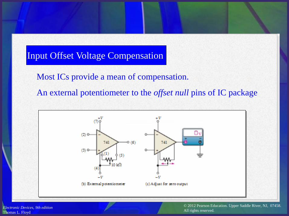
Input Offset Voltage Compensation
Most ICs provide a mean of compensation.
An external potentiometer to the offset null pins of IC package
© 2012 Pearson Education. Upper Saddle River, NJ, 07458.
All rights reserved. Electronic Devices, 9th edition
Thomas L. Floyd
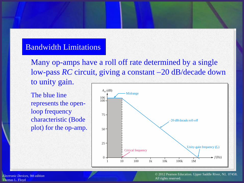
Bandwidth Limitations
Many op-amps have a roll off rate determined by a single
low-pass RC circuit, giving a constant -20 dB/decade down
to unity gain.
–20 dB/decade roll-off
Unity-gain frequency (fT)Critical frequency
101 100 1k 10k 100k 1M
f (Hz)
106100
75
50
25
0
Aol (dB)MidrangeThe blue line
represents the open-
loop frequency
characteristic (Bode
plot) for the op-amp.
© 2012 Pearson Education. Upper Saddle River, NJ, 07458.
All rights reserved. Electronic Devices, 9th edition
Thomas L. Floyd
Bandwidth Limitations
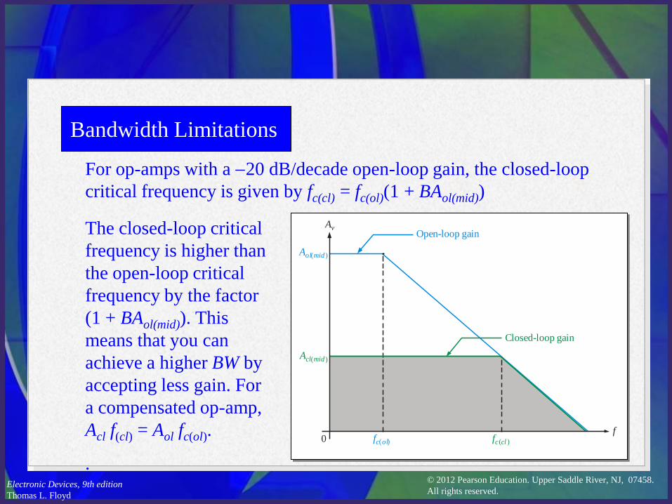
For op-amps with a -20 dB/decade open-loop gain, the closed-loop
critical frequency is given by fc(cl) = fc(ol)(1 + BAol(mid))
The closed-loop critical
frequency is higher than
the open-loop critical
frequency by the factor
(1 + BAol(mid)). This
means that you can
achieve a higher BW by
accepting less gain. For
a compensated op-amp,
Acl f(cl) = Aol fc(ol).
.
Av
f
Aol(mid )
0 fc(ol) fc(cl )
Acl(mid )
Closed-loop gain
Open-loop gain
© 2012 Pearson Education. Upper Saddle River, NJ, 07458.
All rights reserved. Electronic Devices, 9th edition
Thomas L. Floyd
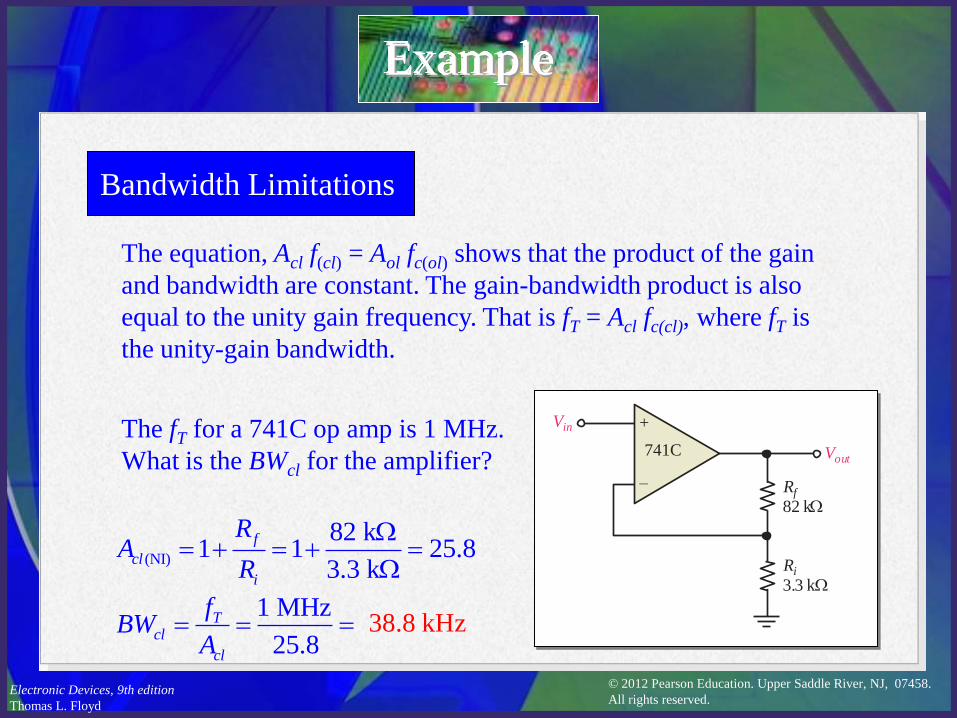
Example
Bandwidth Limitations
The equation, Acl f(cl) = Aol fc(ol) shows that the product of the gain
and bandwidth are constant. The gain-bandwidth product is also
equal to the unity gain frequency. That is fT = Acl fc(cl), where fT is
the unity-gain bandwidth.
The fT for a 741C op amp is 1 MHz.
What is the BWcl for the amplifier? Rf
82 kW
Vin +
–
Vout
Ri
3.3 kW
741C
(NI)
82 k1 1 25.8
3.3 k
f
cl
i
RA
R
W
W
1 MHz
25.8
Tcl
cl
fBW
A 38.8 kHz
© 2012 Pearson Education. Upper Saddle River, NJ, 07458.
All rights reserved. Electronic Devices, 9th edition
Thomas L. Floyd
Selected Key Terms
Operational
amplifier
Differential
mode
Common mode
A type of amplifier that has very high voltage
gain, very high input impedance, very low
output impedance and good rejection of
common-mode signals.
A mode of op-amp operation in which two
opposite-polarity signals voltages are applied to
the two inputs (double-ended) or in which a
signal is applied to one input and ground to the
other input (single-ended).
A condition characterized by the presence of
the same signal on both inputs
© 2012 Pearson Education. Upper Saddle River, NJ, 07458.
All rights reserved. Electronic Devices, 9th edition
Thomas L. Floyd
Selected Key Terms
Open-loop
voltage gain
Negative
feedback
Closed-loop
voltage gain
Gain-
bandwidth
product
The voltage gain of an op-amp without external
feedback.
The process of returning a portion of the output
signal to the input of an amplifier such that it is
out of phase with the input.
The voltage gain of an op-amp with external
feedback.
A constant parameter which is always equal to
the frequency at which the op-amp’s open-loop
gain is unity (1).