UUUU - crystage.com · UUULTRA CCCHIP High-Voltage Mixed-Signal IC ©1999 ~ 2009 6 MP...
75
N MP Specifications July 3, 2009 Revision 1.43 ULTRA LTRA LTRA LTRACHIP HIP HIP HIP The Coolest LCD Driver. Ever!! 160COM x 256SEG Matrix LCD Controller-Driver w/ 16-shade per pixel HIGH-VOLTAGE MIXED-SIGNAL IC
Transcript of UUUU - crystage.com · UUULTRA CCCHIP High-Voltage Mixed-Signal IC ©1999 ~ 2009 6 MP...

N
MP Specifications July 3, 2009 Revision 1.43
UUUULTRALTRALTRALTRACCCCHIPHIPHIPHIP The Coolest LCD Driver. Ever!!
160COM x 256SEG Matrix LCD Controller-Driver w/ 16-shade per pixel
HIGH-VOLTAGE MIXED-SIGNAL IC

UUUULTRALTRALTRALTRACCCCHIPHIPHIPHIP
High-Voltage Mixed-Signal IC ©1999 ~ 2009
2 MP Specifications
TABLE OF CONTENT
INTRODUCTION.............................................................................................................3
ORDERING INFORMATION...........................................................................................4
BLOCK DIAGRAM .........................................................................................................5
PIN DESCRIPTION.........................................................................................................6
RECOMMENDED COG LAYOUT...................................................................................9
CONTROL REGISTERS...............................................................................................10
COMMAND TABLE ......................................................................................................13
COMMAND DESCRIPTIONS .......................................................................................15
LCD VOLTAGE SETTING ............................................................................................27
VLCD QUICK REFERENCE............................................................................................28
LCD DISPLAY CONTROLS .........................................................................................30
HOST INTERFACE.......................................................................................................33
DISPLAY DATA RAM...................................................................................................43
WINDOW PROGRAM...................................................................................................44
RESET & POWER MANAGEMENT .............................................................................47
MULTI-TIME PROGRAM NV MEMORY .......................................................................49
MTP OPERATION FOR LCM MAKERS .......................................................................50
SAMPLE COMMAND SEQUENCES ............................................................................54
ESD CONSIDERATION................................................................................................55
ABSOLUTE MAXIMUM RATINGS ...............................................................................56
SPECIFICATIONS ........................................................................................................57
AC CHARACTERISTICS..............................................................................................58
PHYSICAL DIMENSIONS.............................................................................................64
ALIGNMENT MARK INFORMATION ...........................................................................65
PAD COORDINATES ...................................................................................................66
TRAY INFORMATION ..................................................................................................72
REVISION HISTORY ....................................................................................................74

UC1611S 160x256/16S Matrix LCD Controller-Driver
Revision A1.43 3
UC1611s Single-Chip, Ultra-Low Power 160COM x 256SEG Matrix Passive LCD Controller-Driver
INTRODUCTION UC1611s is an advanced high-voltage mixed-signal CMOS IC, especially designed for the display needs of ultra-low power hand-held devices.
UC1611s employs UltraChip’s unique DCC (Direct Capacitor Coupling) driver architecture and LRM (Line Rate Modulation) gray-shade modulation scheme to achieve near crosstalk free images, with well balanced gray shades.
In addition to low power SEG and COM drivers, UC1611s contains all necessary circuits for high-V LCD power supply, bias voltage generation, timing generation, and graphics data memory.
Advanced circuit design techniques are employed to minimize external component counts and reduce connector size while achieving extremely low power consumption.
MAIN APPLICATIONS
• Cellular Phones, Smart Phones, PDA, and other battery-operated palmtop devices and/or portable instruments.
FEATURE HIGHLIGHTS
• Single-chip controller-driver supports 160x256 STN LCD, 16-shade-per-pixel with gamma compensated modulation.
• Soft-ICON: Partial scroll function to support programmable graphics ICON or scroll bar.
• Support both row ordered and column ordered display buffer RAM access
• Support industry standard 4-wire, 3-wire, and 2-wire serial buses (S8, S9, I2C), and 16- /8- /4-bit parallel buses (8080 or 6800).
• Special driver structure and gray shade modulation scheme produce near crosstalk free image, with low power consumption for all display patterns.
• Fully programmable Mux Rate, partial display window, Bias Ratio, and Line Rate allow many flexible power management options.
• 4 software programmable frame rates (25Hz, 30Hz, 35Hz, and 40Hz). Support the use of fast Liquid Crystal material for speedy LCD response.
• 4 software-programmable temperature compensation coefficients.
• On-chip Power-ON Reset and Software RESET command make RST pin optional.
• Self-configuring 11x charge pump with on-chip pumping capacitor requires only 5 external capacitors to operate.
• Flexible data addressing/mapping schemes to support wide ranges of software models and LCD layout placements.
• VDD (digital) range (Typ.): 1.8 V ~ 3.3V VDD (analog) range (Typ.): 2.8 V ~ 3.3V LCD VOP range: 5.65V ~ 17.5V
• Available in gold bump dies Bump pitch: 38 µM (Typ.) Bump gap: 13 µM (Typ.) Bump surface: 1887.5 µM2

UUUULTRALTRALTRALTRACCCCHIPHIPHIPHIP
High-Voltage Mixed-Signal IC ©1999 ~ 2009
4 MP Specifications
ORDERING INFORMATION
Product ID Description
UC1611sGAA Gold bumped die.
General Notes
APPLICATION INFORMATION
For improved readability, the specification contains many application data points. When application information is given, it is advisory and does not form part of the specification for the device.
BARE DIE DISCLAIMER
All die are tested and are guaranteed to comply with all data sheet limits up to the point of wafer sawing. There is no post waffle saw/pack testing performed on individual die. Although the latest modern processes are utilized for wafer sawing and die pick-&-place into waffle pack carriers, UltraChip has no control of third party procedures in the handling, packing or assembly of the die. Accordingly, it is the responsibility of the customer to test and quality their application in which the die is to be used. UltraChip assumes no liability for device functionality or performance of the die or systems after handling, packing or assembly of the die.
USE OF I2C
The implementation of I2C is already included and tested in all silicon.
MTP LIGHT & ESD SENSITIVITY
The MTP memory cell is sensitive to photon excitation and ESD. Under extended exposure to strong ambient light, or when TST4 pin is exposed to ESD strikes, the MTP cells can lose its content before the specified memory retention time span. The system designer is advised to provide proper light & ESD shields to realize full MTP content retention performance. LIFE SUPPORT APPLICATIONS
These devices are not designed for use in life support appliances, or systems where malfunction of these products can reasonably be expected to result in personal injuries. Customer using or selling these products for use in such applications do so at their own risk.
CONTENT DISCLAIMER
UltraChip believes the information contained in this document to be accurate and reliable. However, it is subject to change without notice. No responsibility is assumed by UltraChip for its use, nor for infringement of patents or other rights of third parties. No part of this publication may be reproduced, or transmitted in any form or by any means without the prior consent of UltraChip Inc. UltraChip's terms and conditions of sale apply at all times.
CONTACT INFORMATION
UltraChip Inc. (Headquarter) 2F, No. 70, Chowtze Street, Nei Hu District, Taipei 114, Taiwan, R. O. C.
Tel: +886 (2) 8797-8947 Fax: +886 (2) 8797-8910 Sales e-mail: [email protected] Web site: http://www.ultrachip.com

UC1611S 160x256/16S Matrix LCD Controller-Driver
Revision A1.43 5
BLOCK DIAGRAM
DISPLAY DATA RAM
COLUMN ADDRESS GENERATOR
DISPLAY DATA LATCHES
LEVEL SHIFTERS
SEG DRIVERS
DA
TA R
AM
I/O
BU
FF
ER
PA
GE
AD
DR
ES
S G
EN
ER
AT
OR
RO
W A
DD
RE
SS
GE
NE
RA
TO
R
LEV
EL
SH
IFT
ER
CO
M D
RIV
ER
S
VLCD & BIAS
GENERATOR HOST INTERFACE
COMMAND
CONTROL & STATUS
REGISTER
CLOCK & TIMING
GENERATOR
POWER ON & RESET
CONTROL
CA1 CA0
CL
CB1 CB0

UUUULTRALTRALTRALTRACCCCHIPHIPHIPHIP
High-Voltage Mixed-Signal IC ©1999 ~ 2009
6 MP Specifications
PIN DESCRIPTION
Name Type Pins Description
MAIN POWER SUPPLY
VDD
VDD2 VDD3
PWR 11 10 4
VDD2/VDD3 is the analog power supply and it should be connected to the same power source. VDD is the digital power supply and it should be connected to a voltage source that is no higher than VDD2/VDD3. Please maintain the following relationship:
VDD+1.5 V VDD2/3 VDD Minimize the trace resistance for VDD and VDD2/VDD3.
VSS
VSS2 GND 11
11 Ground. Connect VSS and VSS2 to the shared GND pin. Minimize the trace resistance for VSS and VSS2.
LCD POWER SUPPLY
VA0+, VA0–
VA1+, VA1–
VB0+, VB0–
VB1+, VB1–
PWR
4, 4 4, 4 4, 4 4, 4
LCD Bias Voltages. These are the voltage sources to provide SEG driving currents. These voltages are generated internally. Connect capacitors of CAX / CBX value between VAX+ / VBX+ and VAX– / VBX–, respectively.
The resistance of these traces directly affects the driving strength of SEG electrodes and impacts the image of the LCD module. Minimize the trace resistance is critical in achieving high quality image.
VLCD-IN
VLCD-OUT PWR 2 2
High voltage LCD Power Supply. Connect these pins together.
A bypass capacitor CL should be connected between VLCD and VSS. Keep the trace resistance under 30 Ω ~ 50 Ω.
Note:
Recommended capacitor values: CA, CB: 100~250 x LCD load capacitance or 5 µF (5V), whichever is higher. CL: 0.1µF ~0.5 µF (25V) is appropriate for most applications.

UC1611S 160x256/16S Matrix LCD Controller-Driver
Revision A1.43 7
Name Type Pins Description
HOST INTERFACE
BM1~0 I 2
Bus Mode: The interface bus mode is determined by BM[1:0] and D[15, 13] with the following relationship:
Mode BM[1:0] DB15, DB13
8080 00 Data
6800 16-bit
01 Data
8080 10 00
6800 8-bit
11 00
8080 10 01
6800 4-bit
11 01
4-wire SPI (S8) 10 10
3-wire SPI (S9) 11 10
2-wire SPI (I2C) 11 11 CS1/A3 CS0/A2 I 2 Chip Selection. Chip is selected when CS1=”H” and CS0 = “L”. When the
chip is not selected, D[15:0] will be high impedance.
RST I 1
When RST=”L”, all control registers are re-initialized with their default states.
An RC filter has been included on-chip. There is no need for external RC noise filter. When RST is not used, connect the pin to VDD.
CD I 1 Control data or Display data Selection for read/write operation. In S9 and I2C modes, CD pin is not used, connect CD pin to VSS. ”L”: Control data ”H”: Display data
WR0 WR1 I 1
1
WR[1:0] controls the read/write operation of the host interface. See Host Interface section for more detail.
In parallel mode, WR[1:0] meaning depends on whether the interface is in 6800 mode or 8080 mode. In serial interface modes, these two pins are not used. Connect them to VSS.
D15~D0 I/O 16
Bi-directional bus for parallel host interface. In serial modes, connect D[0] to SCK, D[3] to SDA, and D[15, 13] to VDD or VSS.
D15 D14 D13 D12 D11 D10 D9 D8 D7 D6 D5 D4 D3 D2 D1 D0
16-bit (BM=0x)
DB[15:0]
8-bit (BM=1x)
0 – 0 – – – – – DB[7:0]
4-bit (BM=1x)
0 – 1 – – – – – – – – – DB[3:0]
S8/S9 (BM=1x)
1 – 0 – – – – – – – – – SDA – – SCK
I2C (BM=11)
1 – 1 – – – – – – – – – SDA – – SCK
Connect unused pins to VSS or VDD. For connection details, refer to the table in the Host Interface section.

UUUULTRALTRALTRALTRACCCCHIPHIPHIPHIP
High-Voltage Mixed-Signal IC ©1999 ~ 2009
8 MP Specifications
Name Type Pins Description
ID0 I 1 Production control. The connection will affect the content of ID when using the Get Status command. Connect to VDD for “H” or VSS for “L”.
ID1 I 1
SEG selection. Window commands will adjust its upper bound of column accordingly. 0 : number of column is set to 256 (SEG0~255) 1 : use SEG0~239 only and leave SEG240~255 open.
HIGH VOLTAGE LCD DRIVER OUTPUT
SEG1 ~ SEG256 HV 256 SEG (column) driver outputs. Support up to 256 columns.
Leave unused drivers open-circuit.
COM1~ COM160 HV 160 COM (row) driver outputs. Support up to 160 rows.
Leave unused drivers open-circuit.
MISC. PINS
VDDX O 5
Auxiliary VDD. These pins are connected to the main VDD bus on chip. They are provided to facilitate chip configurations in COG application. These pins should not be used to provide VDD power to the chip. It is not necessary to connect VDDX to main VDD externally.
TST4 I/HV 2
TST4 controls test mode and is also used to supply one of the high voltage required for MTP Program operation. Leave TST4 open during normal LCD operation. In COG applications keep TST4 trace resistance between 30 Ω ~ 50 Ω.
TST2 TST1 I/O 1
1 Test I/O pins. Leave these pins open during normal use.
Dummy 13 Dummy pins are NOT connected inside the IC.
Note: Several control registers will specify “0-based index” for COM and SEG electrodes. In those situations,
COMX or SEGX will correspond to index X-1, and the value ranges for those index registers will be 0~159 for COM and 0~255 for SEG.

UC1611S 160x256/16S Matrix LCD Controller-Driver
Revision A1.43 9
RECOMMENDED COG LAYOUT
DUMMY2
COM_pad<101>COM_pad<103>
COM_pad<105>COM_pad<107>COM_pad<109>COM_pad<111>COM_pad<113>COM_pad<115>COM_pad<117>
COM_pad<119>COM_pad<121>COM_pad<123>
COM_pad<125>COM_pad<127>COM_pad<129>COM_pad<131>COM_pad<133>COM_pad<135>COM_pad<137>
COM_pad<139>COM_pad<141>COM_pad<143>
COM_pad<145>COM_pad<147>COM_pad<149>COM_pad<151>COM_pad<153>COM_pad<155>COM_pad<157>COM_pad<159>
D15
Vddx
D14
D13
D12
D11
D10
D9
D8
D7
D6
D5
D4
D3
D2
D1
D0
RST
CS0
vddx
CS1
CD
WR0
Vddx
WR1
BM1
Vddx
BM0
TST4
TST4
ID0
Vddx
ID1
VSS
VSS
VSS
VSS
VSS
VSS
VSS
VSS
VSS
VSS
VSS
VSS2
VSS2
VSS2
VSS2
VSS2
VSS2
VSS2
VSS2
VSS2
VSS2
VSS2
VDD2
VDD2
VDD2
VDD2
VDD2
VDD2
VDD2
VDD2
VDD2
VDD2
DUMMY5
VDD3
VDD3
VDD3
VDD3
VDD
VDD
VDD
VDD
VDD
VDD
VDD
VDD
VDD
VDD
VDD
DUMMY6
DUMMY7
DUMMY8
DUMMY9
DUMMY10
DUMMY11
DUMMY12
DUMMY13
TST2
TST1
VLCDIN
VLCDIN
VLCDOUT
VLCDOUT
VA0-
VA0-
VA0-
VA0-
VA1-
VA1-
VA1-
VA1-
VA1+
VA1+
VA1+
VA1+
VA0+
VA0+
VA0+
VA0+
VB0-
VB0-
VB0-
VB0-
VB1-
VB1-
VB1-
VB1-
VB1+
VB1+
VB1+
VB1+
VB0+
VB0+
VB0+
VB0+
COM_pad<160>COM_pad<158>COM_pad<156>COM_pad<154>COM_pad<152>COM_pad<150>COM_pad<148>COM_pad<146>COM_pad<144>COM_pad<142>
COM_pad<140>COM_pad<138>COM_pad<136>
COM_pad<134>COM_pad<132>COM_pad<130>COM_pad<128>COM_pad<126>COM_pad<124>COM_pad<122>COM_pad<120>
COM_pad<118>COM_pad<116>COM_pad<114>
COM_pad<112>COM_pad<110>COM_pad<108>
COM_pad<106>COM_pad<104>COM_pad<102>
DUMMY3 DUMMY4
COM_pad<100>COM_pad<98>COM_pad<96>COM_pad<94>COM_pad<92>COM_pad<90>COM_pad<88>
COM_pad<86>COM_pad<84>COM_pad<82>
COM_pad<80>COM_pad<78>COM_pad<76>COM_pad<74>
COM_pad<72>COM_pad<70>COM_pad<68>COM_pad<66>COM_pad<64>COM_pad<62>COM_pad<60>
COM_pad<58>COM_pad<56>COM_pad<54>
COM_pad<52>COM_pad<50>COM_pad<48>COM_pad<46>COM_pad<44>COM_pad<42>COM_pad<40>
COM_pad<38>COM_pad<36>COM_pad<34>
COM_pad<32>COM_pad<30>COM_pad<28>COM_pad<26>COM_pad<24>COM_pad<22>COM_pad<20>
COM_pad<18>COM_pad<16>COM_pad<14>
COM_pad<12>COM_pad<10>COM_pad<8>COM_pad<6>COM_pad<4>COM_pad<2>SEG_pad<1>SEG_pad<2>SEG_pad<3>SEG_pad<4>SEG_pad<5>
SEG_pad<6>SEG_pad<7>SEG_pad<8>
SEG_pad<9>SEG_pad<10>SEG_pad<11>SEG_pad<12>SEG_pad<13>SEG_pad<14>SEG_pad<15>
SEG_pad<16>SEG_pad<17>SEG_pad<18>
SEG_pad<19>SEG_pad<20>SEG_pad<21>
SEG_pad<22>SEG_pad<23>SEG_pad<24>SEG_pad<25>SEG_pad<26>SEG_pad<27>SEG_pad<28>
SEG_pad<29>SEG_pad<30>SEG_pad<31>
SEG_pad<32>SEG_pad<33>SEG_pad<34>SEG_pad<35>SEG_pad<36>SEG_pad<37>SEG_pad<38>SEG_pad<39>
SEG_pad<40>SEG_pad<41>SEG_pad<42>
SEG_pad<43>SEG_pad<44>SEG_pad<45>
SEG_pad<46>SEG_pad<47>SEG_pad<48>SEG_pad<49>SEG_pad<50>SEG_pad<51>SEG_pad<52>
SEG_pad<53>SEG_pad<54>SEG_pad<55>
SEG_pad<56>SEG_pad<57>SEG_pad<58>SEG_pad<59>SEG_pad<60>SEG_pad<61>SEG_pad<62>
SEG_pad<63>SEG_pad<64>SEG_pad<65>
SEG_pad<66>SEG_pad<67>SEG_pad<68>SEG_pad<69>SEG_pad<70>SEG_pad<71>SEG_pad<72>SEG_pad<73>SEG_pad<74>SEG_pad<75>SEG_pad<76>
SEG_pad<77>SEG_pad<78>SEG_pad<79>
SEG_pad<80>SEG_pad<81>SEG_pad<82>SEG_pad<83>SEG_pad<84>SEG_pad<85>SEG_pad<86>
SEG_pad<87>SEG_pad<88>SEG_pad<89>
SEG_pad<90>SEG_pad<91>SEG_pad<92>SEG_pad<93>SEG_pad<94>SEG_pad<95>SEG_pad<96>
SEG_pad<97>SEG_pad<98>SEG_pad<99>
SEG_pad<100>SEG_pad<101>SEG_pad<102>
SEG_pad<103>SEG_pad<104>SEG_pad<105>SEG_pad<106>SEG_pad<107>SEG_pad<108>SEG_pad<109>SEG_pad<110>
SEG_pad<111>SEG_pad<112>SEG_pad<113>
SEG_pad<114>SEG_pad<115>SEG_pad<116>SEG_pad<117>SEG_pad<118>SEG_pad<119>SEG_pad<120>SEG_pad<121>SEG_pad<122>SEG_pad<123>
SEG_pad<124>SEG_pad<125>SEG_pad<126>
SEG_pad<127>SEG_pad<128>SEG_pad<129>SEG_pad<130>SEG_pad<131>SEG_pad<132>SEG_pad<133>
SEG_pad<134>SEG_pad<135>SEG_pad<136>
SEG_pad<137>SEG_pad<138>SEG_pad<139>SEG_pad<140>SEG_pad<141>SEG_pad<142>SEG_pad<143>
SEG_pad<144>SEG_pad<145>SEG_pad<146>
SEG_pad<147>SEG_pad<148>SEG_pad<149>SEG_pad<150>SEG_pad<151>SEG_pad<152>SEG_pad<153>SEG_pad<154>SEG_pad<155>SEG_pad<156>SEG_pad<157>
SEG_pad<158>SEG_pad<159>SEG_pad<160>
SEG_pad<161>SEG_pad<162>SEG_pad<163>SEG_pad<164>SEG_pad<165>SEG_pad<166>SEG_pad<167>
SEG_pad<168>SEG_pad<169>SEG_pad<170>
SEG_pad<171>SEG_pad<172>SEG_pad<173>SEG_pad<174>SEG_pad<175>SEG_pad<176>SEG_pad<177>SEG_pad<178>SEG_pad<179>SEG_pad<180>
SEG_pad<181>SEG_pad<182>SEG_pad<183>
SEG_pad<184>SEG_pad<185>SEG_pad<186>SEG_pad<187>SEG_pad<188>SEG_pad<189>SEG_pad<190>SEG_pad<191>
SEG_pad<192>SEG_pad<193>SEG_pad<194>
SEG_pad<195>SEG_pad<196>SEG_pad<197>
SEG_pad<198>SEG_pad<199>SEG_pad<200>SEG_pad<201>SEG_pad<202>SEG_pad<203>SEG_pad<204>
SEG_pad<205>SEG_pad<206>SEG_pad<207>
SEG_pad<208>SEG_pad<209>SEG_pad<210>SEG_pad<211>SEG_pad<212>SEG_pad<213>SEG_pad<214>
SEG_pad<215>SEG_pad<216>SEG_pad<217>
SEG_pad<218>SEG_pad<219>SEG_pad<220>SEG_pad<221>SEG_pad<222>SEG_pad<223>SEG_pad<224>SEG_pad<225>SEG_pad<226>SEG_pad<227>SEG_pad<228>
SEG_pad<229>SEG_pad<230>SEG_pad<231>
SEG_pad<232>SEG_pad<233>SEG_pad<234>SEG_pad<235>SEG_pad<236>SEG_pad<237>SEG_pad<238>
SEG_pad<239>SEG_pad<240>SEG_pad<241>
SEG_pad<242>SEG_pad<243>SEG_pad<244>SEG_pad<245>SEG_pad<246>SEG_pad<247>SEG_pad<248>
SEG_pad<249>SEG_pad<250>SEG_pad<251>
SEG_pad<252>SEG_pad<253>SEG_pad<254>
SEG_pad<255>SEG_pad<256>COM_pad<1>COM_pad<3>COM_pad<5>COM_pad<7>COM_pad<9>COM_pad<11>
COM_pad<13>COM_pad<15>COM_pad<17>
COM_pad<19>COM_pad<21>COM_pad<23>COM_pad<25>COM_pad<27>COM_pad<29>COM_pad<31>COM_pad<33>COM_pad<35>COM_pad<37>
COM_pad<39>COM_pad<41>COM_pad<43>
COM_pad<45>COM_pad<47>COM_pad<49>COM_pad<51>COM_pad<53>COM_pad<55>COM_pad<57>
COM_pad<59>COM_pad<61>COM_pad<63>
COM_pad<65>COM_pad<67>COM_pad<69>COM_pad<71>COM_pad<73>COM_pad<75>COM_pad<77>
COM_pad<79>COM_pad<81>COM_pad<83>
COM_pad<85>COM_pad<87>COM_pad<89>COM_pad<91>COM_pad<93>COM_pad<95>COM_pad<97>COM_pad<99>
DUMMY1
UC
1611s Bum
p View
ID1
ID0
TST4
BM0
BM1
WR1
WR0
CD
CS0
RST
D0
D1
D2
D3
D4
D5
D6
D7
D8
D9
D10
D11
D12
D13
D14
D15
VSS
VDD
VLCD
VA0-
VA1-
VA1+
VA0+
VB0-
VB1-
VB1+
VB0+
Note for VDD and VSS with COG: The operation condition, VDD=1.8V (typical), should be satisfied under all operating conditions. UC1611s’ peak current (IDD) can be up to ~15mA during high speed data-write to UC1611s’ on-chip SRAM. Such high pulsing current mandates very careful design of VDD and VSS ITO trances in COG modules. When VDD and VSS trace resistance is not low enough, the pulsing IDD current can cause the actual on-chip VDD to drop to below 1.65V and cause the IC to malfunction.

UUUULTRALTRALTRALTRACCCCHIPHIPHIPHIP
High-Voltage Mixed-Signal IC ©1999 ~ 2009
10 MP Specifications
CONTROL REGISTERS UC1611s contains registers that control the chip operation. These registers can be modified by commands. The following table is a summary of the control registers, their meaning and their default value. Commands supported by UC1611s will be described in the next two sections. A summary table comes first and then followed by a detailed instruction-by-instruction description.
Name: The symbolic reference of the register. Note that, some symbol names refer to bits (flags) within another register.
Default: Numbers shown in Bold font are default values after Power-Up-Reset and System-Reset.
Name Bits Default Description
SL 8 00H Scroll Line. Scroll the displayed image up by SL rows. The valid SL value are between 0 (for no scrolling) and (159 – FL). Setting SL outside of this range causes undefined effect on the displayed image.
FL 4 0H Fixed lines. The first (FLx2) lines of each frame are fixed and are not affected by scrolling (SL). When FL is non-zero, the screen is effectively separated into two regions: one scrollable, one non-scrollable.
CA 8 00H Display Data RAM Column Address (Used in Host to Display Data RAM access)
PA 7 00H Display Data RAM Page Address (Used in Host for Display Data RAM access) When DC[5:3] = 100b,
PA[6:5] : used to select Write Pattern 0~3. PA[4:0] : set SRAM page address
BR 2 2H Bias Ratio. The ratio between VLCD and VBIAS. 00b: 5 01b: 10 10b: 11 11b: 12
TC 2 0H Temperature Compensation (per oC). 00b: -0.05% 01b: -0.10% 10b: -0.15% 11b: 0.00%
PM 8 EAH Electronic Potentiometer to fine tune VBIAS and VLCD
PMO 6 00H PM offset. the effective PM value, PMV = PM - PMO[4:0] when PMO[5]=1 the effective PM value, PMV = PM + PMO[4:0] when PMO[5]=0
PC 4 FH Pump Control. PC[1:0]: Panel Loading 00b: LCD: 33nF 11b: 33nF LCD55nF PC[3:2]: Pump Control 00b: External VLCD 11b: Internal VLCD (11x charge pump)
(Setting to 01 or 10 will be invalid and default value will be used instead.)
AC 4 1H Address Control: AC[0]: WA: Automatic column/page Wrap Around (Default 1:ON) AC[1]: Auto-Increment order
0: Column (CA) first 1: Page (PA) first AC[2]: PID: PA (page address) auto increment direction (0:+1, 1:-1) AC[3]: Window Program Mode
0 : Inside Mode: Write to SRAM within the window defined by (WPC0,WPP0), (WPC1,WPP1) 1 : Outside Mode: Write to SRAM but skip the window defined by (WPC0,WPP0), (WPC1,WPP1)

UC1611S 160x256/16S Matrix LCD Controller-Driver
Revision A1.43 11
Name Bits Default Description
DC 8 18H Display Control: DC[0]: PXV: Pixels Inverse. Bit-wise data inversion. (Default 0:OFF) DC[1]: APO: All Pixels ON (Default 0:OFF) DC[2]: Display ON/OFF (Default 0:OFF) DC[4:3]: Gray-shade Modulation mode. 00 : On/Off mode 01: 8-shade Mode 10 : 4-shade Mode 11: 16-shade mode DC[5]: Input Type of On/Off Mode (enable only when DC[4:3]=00b) 0: 4-bit per 1-pixel 1: 1-bit per 1-pixel DC[7:6]: Display Pattern Selection (enable only when DC[5:3]=100b) 00: Pattern0 01: Pattern1 10: Pattern2 11: Pattern3
LC 10 020H LCD Control: LC[0]: MSF: MSB First mapping Option (Default: 0:OFF) LC[1]: MX, Mirror X. SEG/Column sequence inversion (Default: 0:OFF) LC[2]: MY, Mirror Y. COM/Row sequence inversion (Default: 0:OFF) LC[3]: Enable FL lines in partial display mode.(Default: 0:OFF) LC[5:4]: Line Rate (= Frame-Rate x Mux-Rate)
LC[5:4]=00b 01b 10b 11b
16-shade 20.0 Klps 24.0 28.0 32.0
8-shade 14.1 16.9 19.7 22.5
4-shade 13.3 16.0 18.7 21.4
On/Off mode 5.9 7.1 8.2 9.4
( Klps: Kilo-Line-per-second ) LC[7:6] : Reserved (Default : 00b) LC[9:8] : Partial Display Control 0xb: Disable Mux-rate = CEN+1 (DST and DEN are not used.) 11b: Enabled Mux-rate = DEN-DST+1+LC[3]xFLx2
NIV 7 00H N-Line Inversion NIV[5:0] : 000000b : Disable N-line Inversion NIV[6] : 0b: no-XOR 1b: XOR
CEN DST DEN
8 8 8
9FH 00H 9FH
COM scanning ENd (the last COM with full line cycle, 0-based index) Display STart (the first COM with active scan pulse, 0-based index) Display EDd (the last COM with active scan pulse, 0-based index) Please maintain the following relationship: CEN = (the actual number of pixel rows on the LCD) – 1 CEN DEN DST+ 9
ISOF 4 1H Set the ISOlation clock in Front of COM pulse.
ISOB 4 0H Set the ISOlation clock in Back of COM pulse.
WPC0 8 00H Window program starting column address. Value range: 0 ~255.
WPP0 7 00H Window program starting page address. Value range: 0~79. When DC[5:3]=100b, value range: 0~19
WPC1 8 FFH Window program ending column address. Value range: 0~255.
WPP1 7 4FH Window program ending page address. Value range: 0~79. When DC[5:3]=100b, value range: 0~19

UUUULTRALTRALTRALTRACCCCHIPHIPHIPHIP
High-Voltage Mixed-Signal IC ©1999 ~ 2009
12 MP Specifications
Name Bits Default Description
MTPC 6 10H
MTP Programming Control: MTPC[2:0] : MTP command 000 : Idle 001 : Read 010 : Erase 011 : Program 1xx : For UltraChip debug use only MTPC[3] : 0: MTP Disabled 1 : Enabled (automatically cleared after each MTP command) MTPC[4] : Ignore/Use MTP. 0: Ignore 1: Use MTPC[5] : For testing only. Set to 0 for normal operation.
MTPM 6 00H MTP Write Mask.. 0: no action 1: program When MTPM[x]=1, the x-th bit of the MTP memory will be programmed to 1. MTPM[x]=0 means no write action for the x-th bit, and the content of this bit will not change.
APC 1 N/A Advanced Product Configuration. For UltraChip only. Please do not use.
Status Registers
OM 2 – Operating Modes (Read Only) 00b: Reset 01b: (Not used) 10b: Sleep 11b: Normal
MD 1 – MTP option flag. 0 : for non-MTP version. 1 : for MTP version
MS 1 – MTP programming in-progress
WS 1 – MTP Operation Succeeded

UC1611S 160x256/16S Matrix LCD Controller-Driver
Revision A1.43 13
COMMAND TABLE The following list of host commands is supported by UC1611s
C/D: 0: Control 1: Data W/R: 0: Write cycle 1: Read cycle
# Effective Data bits – Don’t Care
Command C/D W/R D7 D6 D5 D4 D3 D2 D1 D0 Action Default
1. Write Data Byte 1 0 # # # # # # # # Write 1 byte N/A 2. Read Data Byte 1 1 # # # # # # # # Read 1 byte N/A
Ver MX MY WA DE WS MD MS ID[1:0] PMO[5:0] 3. Get Status 0 1
Product Code 0 0 0 EF Get Status N/A
Set Column Addr. LSB 0 0 0 0 0 0 # # # # Set CA[3:0] 0 4.
Set Column Addr. MSB 0 0 0 0 0 1 # # # # Set CA[7:4] 0 5. Temp. Compensation. 0 0 0 0 1 0 0 1 # # Set TC[1:0] 00b: -0.05%/oC 6. Set Panel Loading 0 0 0 0 1 0 1 0 # # Set PC [1:0] 11b: 33~55 nF 7. Set Pump Control 0 0 0 0 1 0 1 1 # # Set PC [3:2] 11b
0 0 1 1 0 0 R R 8. Set Adv. Program Control
(double-byte command) 0 0
# # # # # # # # Set APC[R][7:0]
R = 0~3 N/A
Set Scroll Line LSB 0 1 0 0 # # # # Set SL[3:0] 0 9.
Set Scroll Line MSB 0 0
0 1 0 1 # # # # Set SL[7:4] 0 Set Page Address LSB 0 1 1 0 # # # # Set PA[3:0] 0
10. Set Page Address MSB
0 0 0 1 1 1 0 # # # Set PA[6:4] 0
11. Set Potentiometer (double-byte command) 0 0
1 #
0 #
0 #
0 #
0 #
0 #
0 #
1 #
Set PM[7:0] PM=EAH
1 0 0 0 0 0 1 0 0 0 0 1 0 0 1 1 12. Set Isolation Clock Front 0 0 - - - - # # # #
Set ISOF[3:0] 1H
1 0 0 0 0 0 1 0 0 0 0 1 0 1 0 0 13. Set Isolation Clock Back 0 0 - - - - # # # #
Set ISOB[3:0] 0H
14. Set Partial Display Control 0 0 1 0 0 0 0 1 # # Set LC[9:8] 00b: Disable 15. Set RAM Address Control 0 0 1 0 0 0 1 # # # Set AC[2:0] 001b 16. Set Fixed Lines 0 0 1 0 0 1 # # # # Set FL[3:0] 0 17. Set Line Rate 0 0 1 0 1 0 0 0 # # Set LC[5:4] 10b:28klps 18. Set All-Pixel-ON 0 0 1 0 1 0 0 1 0 # Set DC[1] 0 19. Set Inverse Display 0 0 1 0 1 0 0 1 1 # Set DC[0] 0 20. Set Display Enable 0 0 1 0 1 0 1 # # # Set DC[4:2] 110b
1 1 0 0 0 0 0 0 21. Set LCD Mapping Control
(double-byte command) 0 0
0 0 0 0 # # # # Set LC[3:0] 0
1 1 0 0 1 0 0 0 22. Set N-line Inversion
(double-byte command) 0 0
- # # # # # # # Set NIV[6:0] 00H
23. Set Display Pattern 0 0 1 1 0 1 0 # # # Set DC[7:5] 000b 24. System Reset 0 0 1 1 1 0 0 0 1 0 System Reset N/A 25. NOP 0 0 1 1 1 0 0 0 1 1 No operation N/A
0 0 1 1 1 0 0 1 TT 26.
Set test control (double-byte command) 0 0 # # # # # # # #
For testing only. Do not use.
N/A
27. Set LCD Bias Ratio 0 0 1 1 1 0 1 0 # # Set BR[1:0] 10b: 11
28. Set COM End 0 0
0 0
1 #
1 #
1 #
1 #
0 #
0 #
0 #
1 # Set CEN[7:0] 159
29. Set Partial Display Start 0 0
0 0
1 #
1 #
1 #
1 #
0 #
0 #
1 #
0 #
Set DST[7:0] 0
30. Set Partial Display End 0 0
0 0
1 #
1 #
1 #
1 #
0 #
0 #
1 #
1 # Set DEN[7:0] 159

UUUULTRALTRALTRALTRACCCCHIPHIPHIPHIP
High-Voltage Mixed-Signal IC ©1999 ~ 2009
14 MP Specifications
Command C/D W/R D7 D6 D5 D4 D3 D2 D1 D0 Action Default
1 1 1 1 0 1 0 0 31.
Set Window Program Starting Column Address 0 0
# # # # # # # # Set
WPC0 0
1 1 1 1 0 1 0 1 32.
Set Window Program Starting Page Address 0 0
- # # # # # # # Set
WPP0 0
1 1 1 1 0 1 1 0 33.
Set Window Program Ending Column Address 0 0
# # # # # # # # Set
WPC1 255
1 1 1 1 0 1 1 1 34. Set Window Program
Ending Page Address 0 0
- # # # # # # #
Shared with MTP
Commands
Set WPP1
79
35. Set Window Program Mode 0 0 1 1 1 1 1 0 0 # Set AC[3] 0:Inside 1 0 1 1 1 0 0 0
36. Set MTP Operation Control 0 0 - - # # # # # #
Set MTPC[5:0] 10H
1 0 1 1 1 0 0 1 37. Set MTP Write Mask 0 0
- - # # # # # # Set MTPM[5:0] 0
1 1 1 1 0 1 0 0 38. Set VMTP1 Potentiometer 0 0
# # # # # # # # Set
MTP1 N/A
1 1 1 1 0 1 0 1 39. Set VMTP2 Potentiometer 0 0
# # # # # # # # Set
MTP2 N/A
1 1 1 1 0 1 1 0 40. Set MTP Write Timer 0 0
# # # # # # # # Set
MTP3 N/A
1 1 1 1 0 1 1 1 41. Set MTP Read Timer 0 0
# # # # # # # #
Shared with Window Program
Commands
Set MTP4
N/A
SERIAL READ COMMAND (ENABLE IN S8 OR S9 BUS MODES ONLY) 0 0 1 1 1 1 1 1 1 0
Ver MX MY WA DE WS MD MS ID[1:0] PMO[5:0]
42. Get Status - 1
Product Code 0 0 0 EF
Get Status till Chip Disable
N/A
Notes:
• All bit patterns other than commands listed above may result in undefined behavior.
• Commands (38)~(41) are shared with commands (31)~(34), and have exactly the same code. When MTPC[3]=0, commands (37)~(41) are interpreted as Window Programming commands. When MTPC[3]=1, they are MTP Control commands.
• MTPM and PM are actually the same register. Only one of the commands (36) is valid at any time, and it is determined by MTPC[3].
• After MTP-ERASE or MTP-PROGRAM operation, please always perform the following steps, a) Disconnect TST4 power source. b) Do a full VDD ON-OFF cycle (make sure VDD drops below 50mV). before resuming normal operation.

UC1611S 160x256/16S Matrix LCD Controller-Driver
Revision A1.43 15
COMMAND DESCRIPTIONS
(1) WRITE DATA TO DISPLAY MEMORY
Action C/D W/R D7 D6 D5 D4 D3 D2 D1 D0
Write data 1 0 8-bit Data-Write to SRAM
(2) READ DATA FROM DISPLAY MEMORY
Action C/D W/R D7 D6 D5 D4 D3 D2 D1 D0
Read data 1 1 8-bit Data-Read from SRAM
Write/Read Data Byte (command 1, 2) operation accesses display buffer RAM based on Page Address (PA) register and Column Address (CA) register. To minimize bus interface cycles, PA and CA will increase or decrease automatically after each bus cycle, depending on the setting of Access Control (AC) register. PA and CA can also be programmed directly by issuing Set Page Address and Set Column Address commands.
If Wrap-Around (WA) is OFF (AC[0] = 0), CA will stop increasing after reaching the end of page, and system programmers need to set the values of PA and CA explicitly. If WA is ON (AC[0]=1), when CA reaches end of page, CA will be reset to 0 and PA will be increased or decreased by 1, depending on the setting of Page Increment Direction (PID, AC[2]). When PA reaches the boundary of RAM (i.e. PA = 0 or 79), PA will be wrapped around to the other end of RAM and continue.
For both 8-bit and 16-bit interfaces, the first 1 byte and 2 bytes Read respectively is a dummy Read. Please ignore the data read out.
(3) GET STATUS SUMMARY
Action C/D W/R D7 D6 D5 D4 D3 D2 D1 D0
Ver MX MY WA DE WS MD MS
ID[1:0] PMO[5:0] Get Status 0 1
Product Code 0 0 0 EF Status 1 definitions: Ver : Version Code. 1 MX: Status of register LC[1], mirror X. MY: Status of register LC[2], mirror Y. WA: Status of register AC[0]. Automatic column/row wrap around. DE: Display enable flag. DE=1 when display is enabled WS: MTP Command Succeeded MD: MTP Option (Yes/No) MS: MTP action status
Status 2 definitions: ID: Connection Status of the ID pin, could be used for production identifying. PMO[5:0] : PM offset value
Status 3 definitions: Product Code : 1h EF: ESD Flag. EF=1 when ESD strikes.
If multiple Get Status commands are issued consecutively within one single CD 101 transaction, the Get Status command will return Status1, Status2, Status3, Status1, Status2, Status3, Status1.. alternately.

UUUULTRALTRALTRALTRACCCCHIPHIPHIPHIP
High-Voltage Mixed-Signal IC ©1999 ~ 2009
16 MP Specifications
(4) SET COLUMN ADDRESS
Action C/D W/R D7 D6 D5 D4 D3 D2 D1 D0
Set Column Address LSB CA[3:0] 0 0 0 0 0 0 CA3 CA2 CA1 CA0
Set Column Address MSB CA[4:7] 0 0 0 0 0 1 CA7 CA6 CA5 CA4
Set the SRAM column address for read/write access.
CA possible value: 0 ~ 255
(5) SET TEMPERATURE COMPENSATION
Action C/D W/R D7 D6 D5 D4 D3 D2 D1 D0
Set Temperature Compensation TC[1:0] 0 0 0 0 1 0 0 1 TC1 TC0 Set VBIAS Temperature compensation coefficient (%-per-degree-C) for all 4 temperature compensation curves.
Temperature compensation curve definition: 00b= -0.05%/oC 01b= -0.10%/oC 10b= -0.15%/oC 11b= 0.00%/oC
(6) SET PANEL LOADING
Action C/D W/R D7 D6 D5 D4 D3 D2 D1 D0
Set Panel Loading PC[1:0] 0 0 0 0 1 0 1 0 PC1 PC0 Set PC[1:0] according to the capacitance loading of LCD panel.
Panel loading definition: 00b : LCD 33nF 11b : 33 nF LCD 55 nF
(7) SET PUMP CONTROL
Action C/D W/R D7 D6 D5 D4 D3 D2 D1 D0
Set Pump Control PC[3:2] 0 0 0 0 1 0 1 1 PC3 PC2 Set PC[3:2] to program the build-in charge pump stages.
00b=External VLCD 11b= Internal VLCD (11x charge pump)
(8) SET ADVANCED PROGRAM CONTROL
Action C/D W/R D7 D6 D5 D4 D3 D2 D1 D0
0 0 0 0 1 1 0 0 0 R Set APC[R][7:0] (Double byte command) 0 0 APC[R] register parameter
For UltraChip only. Please do NOT use.
UC1611S 160x256/16S Matrix LCD Controller-Driver
Revision A1.43 17
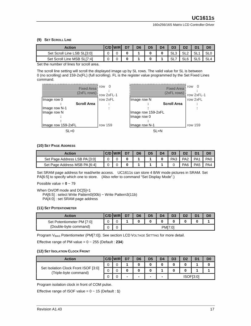
(9) SET SCROLL LINE
Action C/D W/R D7 D6 D5 D4 D3 D2 D1 D0
Set Scroll Line LSB SL[3:0] 0 0 0 1 0 0 SL3 SL2 SL1 SL0
Set Scroll Line MSB SL[7:4] 0 0 0 1 0 1 SL7 SL6 SL5 SL4 Set the number of lines for scroll area.
The scroll line setting will scroll the displayed image up by SL rows. The valid value for SL is between 0 (no scrolling) and 159-2x(FL) (full scrolling). FL is the register value programmed by the Set Fixed Lines command.
Fixed Area (2xFL rows)
row 0 : row 2xFL-1
Fixed Area (2xFL rows)
row 0 : row 2xFL-1
Image row 0 : Scroll Area Image row N-1 Image row N : : Image row 159-2xFL
row 2xFL : : row 159
Image row N : Scroll Area : Image row 159-2xFL Image row 0 : Image row N-1
row 2xFL : : row 159
SL=0 SL=N
(10) SET PAGE ADDRESS
Action C/D W/R D7 D6 D5 D4 D3 D2 D1 D0
Set Page Address LSB PA [3:0] 0 0 0 1 1 0 PA3 PA2 PA1 PA0
Set Page Address MSB PA [6:4] 0 0 0 1 1 1 0 PA6 PA5 PA4
Set SRAM page address for read/write access. UC1611s can store 4 B/W mode pictures in SRAM. Set PA[6:5] to specify which one to store. (Also refer to command “Set Display Mode”.)
Possible value = 0 ~ 79
When On/Off mode and DC[5]=1 PA[6:5] : select Write Pattern0(00b) ~ Write Pattern3(11b) PA[4:0] : set SRAM page address
(11) SET POTENTIOMETER
Action C/D W/R D7 D6 D5 D4 D3 D2 D1 D0
0 0 1 0 0 0 0 0 0 1 Set Potentiometer PM [7:0] (Double-byte command) 0 0 PM[7:0]
Program VBIAS Potentiometer (PM[7:0]). See section LCD VOLTAGE SETTING for more detail.
Effective range of PM value = 0 ~ 255 (Default : 234)
(12) SET ISOLATION CLOCK FRONT
Action C/D W/R D7 D6 D5 D4 D3 D2 D1 D0
0 0 1 0 0 0 0 0 1 0
0 0 0 0 0 1 0 0 1 1 Set Isolation Clock Front ISOF [3:0]
(Triple-byte command) 0 0 - - - - ISOF[3:0]
Program isolation clock in front of COM pulse.
Effective range of ISOF value = 0 ~ 15 (Default : 1)

UUUULTRALTRALTRALTRACCCCHIPHIPHIPHIP
High-Voltage Mixed-Signal IC ©1999 ~ 2009
18 MP Specifications
(13) SET ISOLATION CLOCK BACK
Action C/D W/R D7 D6 D5 D4 D3 D2 D1 D0
0 0 1 0 0 0 0 0 1 0
0 0 0 0 0 1 0 1 0 0 Set Isolation Clock Back ISOB [3:0]
(Triple-byte command) 0 0 - - - - ISOB[3:0]
Program isolation clock in back of COM pulse.
Effective range of ISOB value = 0 ~ 15 (Default : 0)
Note: Use higher VLCD when increase isolation clock.
(14) SET PARTIAL DISPLAY CONTROL
Action C/D W/R D7 D6 D5 D4 D3 D2 D1 D0
Set Partial Display Control LC [9:8] 0 0 1 0 0 0 0 1 LC9 LC8
This command is used to control partial display function.
LC[9:8] : 0xb: Disable Partial Display, Mux-Rate = CEN+1 (DST and DEN are not used.) 11b: Enable Partial Display, Mux-Rate = DEN-DST+1+LC[3]xFLx2
(15) SET RAM ADDRESS CONTROL
Action C/D W/R D7 D6 D5 D4 D3 D2 D1 D0
Set AC [2:0] 0 0 1 0 0 0 1 AC2 AC1 AC0
Program registers AC[2:0] for RAM address control.
AC[0]: WA, Automatic column/page wrap around. 0: CA or PA (depends on AC[1]= 0 or 1) will stop incrementing after reaching boundary 1: CA or PA (depends on AC[1]= 0 or 1) will restart, and PA or CA will increment by one step.
AC[1]: Auto-Increment order 0 : column (CA) increases (+1) first until CA reach CA boundary, then PA will increase by (+/-1). 1 : page (PA) increases (+/-1) first until PA reach PA boundary, then CA will increase by (+1).
AC[2]: PID, page address (PA) auto increment direction (0/1 = +/- 1) When WA=1 and CA reaches CA boundary(CA=MC), PID controls whether page address will be adjusted by increasing +1 or -1. If WA is 0, the column address will stay in MC value and the page address will stay unchanged.
Front Isolation Clock
Back Isolation Clock
COM pulse width

UC1611S 160x256/16S Matrix LCD Controller-Driver
Revision A1.43 19
(16) SET FIXED LINES
Action C/D W/R D7 D6 D5 D4 D3 D2 D1 D0
Set Fixed Lines FL [3:0] 0 0 1 0 0 1 FL3 FL2 FL1 FL0
The Fixed Lines function is used to implement the partial scroll function by dividing the screen into scroll and fixed area. The Set Fixed Lines command will define the fixed area, which will not be affected by the SL scroll function. When MY= 0, the fixed area covers the top 2xFL rows; when MY=1, the bottom 2xFL rows. One example of the visual effect on LCD is illustrated in the figure below. Default : 0.
MY = 0 MY = 1
(17) SET LINE RATE
Action C/D W/R D7 D6 D5 D4 D3 D2 D1 D0
Set Line Rate LC [5:4] 0 0 1 0 1 0 0 0 LC5 LC4
Program LC [5:4] for line rate setting (Line-Rate = Frame-Rate x Mux-Rate)
In 16-shade mode: 00b : 20.0 Klps 01b : 24.0 Klps 10b : 28.0 Klps 11b : 32.0 Klps In 8-shade mode: 00b : 14.1 Klps 01b : 16.9 Klps 10b : 19.7 Klps 11b : 22.5 Klps In 4-shade mode: 00b : 13.3 Klps 01b : 16.0 Klps 10b : 18.7 Klps 11b : 21.4 Klps In On/Off mode: 00b : 5.9 Klps 01b : 7.1 Klps 10b : 8.2 Klps 11b : 9.4 Klps (Klps: Kilo-line per second)
(18) SET ALL PIXEL ON
Action C/D W/R D7 D6 D5 D4 D3 D2 D1 D0
Set All Pixel ON DC [1] 0 0 1 0 1 0 0 1 0 DC1 Set DC[1] to force all SEG drivers to output ON signals. This function has no effect on the existing data stored in display RAM. Default: 0.
(19) SET INVERSE DISPLAY (PXV)
Action C/D W/R D7 D6 D5 D4 D3 D2 D1 D0
Set Inverse Display DC [0] 0 0 1 0 1 0 0 1 1 DC0 Set DC[0] to force all SEG drivers to output the inverse of the data (bit-wise) stored in display RAM. This function has no effect on the existing data stored in display RAM. Default: 0.
Fixed Area 1
(2xFL)
Scroll Area
160
1
Scroll Area
Fixed Area
(2xFL) 160

UUUULTRALTRALTRALTRACCCCHIPHIPHIPHIP
High-Voltage Mixed-Signal IC ©1999 ~ 2009
20 MP Specifications
(20) SET DISPLAY ENABLE
Action C/D W/R D7 D6 D5 D4 D3 D2 D1 D0
Set Display Enable DC[4:2] 0 0 1 0 1 0 1 DC4 DC3 DC2 This command is for programming register DC[4:2]. Default : 110b.
When DC[2] is set to 0, the IC will put itself into Sleep mode. All drivers, voltage generation circuit and timing circuit will be halted to conserve power. When DC[2] is set to 1, UC1611s will first exit from Sleep mode, restore the power and then turn on COM drivers and SEG drivers. There is no other explicit user action or timing sequence required to enter or exit the Sleep mode.
DC[4:3] controls the gray shade modulation modes. UC1611s has four gray shade modulation modes: an On/Off mode 8-shade mode, 4-shade mode and a 16-shade mode. The modulation curves are shown below. Horizontal axes are the gray shade data. The vertical axes are the ON-OFF ratio.
Effective range: DC[4:3] Gray-Scale D7 D6 D5 D4 D3 D2 D1 D0
DC[5]=1 1 0 1 0 1 0 1 0 00 DC[5]=0
B/W Mode 1 - - - 0 - - - 1 1 1 - 0 0 0 - 1 1 0 - 0 0 1 - 1 0 1 - 0 1 0 -
01 8-shade
1 0 0 - 0 1 1 - 1 1 - - 0 0 - - 10 4-shade 1 0 - - 0 1 - - 1 1 1 1 0 0 0 0 1 1 1 0 0 0 0 1 1 1 0 1 0 0 1 0 1 1 0 0 0 0 1 1 1 0 1 1 0 1 0 0 1 0 1 0 0 1 0 1 1 0 0 1 0 1 1 0
11 16-shade
1 0 0 0 0 1 1 1 MSF=0 : RAM_D[7:4] = B[7:4], RAM_D[3:0] = B[3:0] MSF=1 : RAM_D[7:4] = B[3:0], RAM_D[3:0] = B[7:4]
0 5
10 15 20 25 30 35 40 45 50
0 1 2 3 4 5 6 7 8 9 10 11 12 13 14 15

UC1611S 160x256/16S Matrix LCD Controller-Driver
Revision A1.43 21
(21) SET LCD MAPPING CONTROL
Action C/D W/R D7 D6 D5 D4 D3 D2 D1 D0
1 1 0 0 0 0 0 0 Set LCD Mapping Control LC[3:0] (Double-byte command)
0 0 0 0 0 0 LC3 MY MX MSF
Set LC[2:0] for COM (row) mirror (MY), SEG (column) mirror (MX) and MSB first or LSB first options (MSF).
MY is implemented by reversing the mapping order between RAM and COM (row) electrodes. The data stored in RAM is not affected by MY command. MY will have immediate effect on the display image.
MX is implemented by selecting the CA or 255-CA as write/read (from host interface) display RAM column address so this function will only take effect after rewriting the RAM data.
MSF is implemented by MSB-LSB swapping. The operation is determined by DC[4:3], as described in Set Gray Scale Mode command below.
LC[3] controls whether the soft icon section (FL on the top) will be displayed during partial display mode.
(22) SET N-LINE INVERSION
Action C/D W/R D7 D6 D5 D4 D3 D2 D1 D0
1 1 0 0 1 0 0 0 Set N-line Inversion NIV [6:0] (Double-byte command)
0 0 - NIV [6:0]
Set N-Line inversion: NIV[5:0]: the number of lines to invert. Default: 000000b NIV[6] : 0b: non-XOR 1b: XOR
(23) SET DISPLAY PATTERN
Action C/D W/R D7 D6 D5 D4 D3 D2 D1 D0
Set Display Pattern 0 0 1 1 0 1 0 DC[7:5] Set Display Pattern Selection: (enabled only when DC[4:3]=00b)
DC[5]: Input type for On/Off mode 0 : 4 bits for 1 pixel 1 : 1 bit for 1 pixel
DC[7:6]: Select Display Pattern (Only enable when On/Off mode and DC[5:3] =100b) 00 : Pattern0 01 : Pattern1 10 : Pattern2 11 : Pattern3
UC1611s can store 4 different patterns in SRAM when DC[5:3]=100. Set PA[6:5] and DC[7:6] to select which pattern to store / display, respectively.
(24) SYSTEM RESET
Action C/D W/R D7 D6 D5 D4 D3 D2 D1 D0
System Reset 0 0 1 1 1 0 0 0 1 0 This command will activate the system reset. Control register values will be reset to their default values. Data stored in RAM will not be affected.
13 2
2
11
11
NIV[6]=1
NIV[6]=0
13 13
13
13
13
13
13
13
13
Frame 1 Frame 2
UUUULTRALTRALTRALTRACCCCHIPHIPHIPHIP
High-Voltage Mixed-Signal IC ©1999 ~ 2009
22 MP Specifications
(25) NOP
Action C/D W/R D7 D6 D5 D4 D3 D2 D1 D0
No operation 0 0 1 1 1 0 0 0 1 1 This command is used for “no operation”.
(26) SET TEST CONTROL
Action C/D W/R D7 D6 D5 D4 D3 D2 D1 D0
0 0 1 1 1 0 0 1 TT Set TT (Double byte command) 0 0 Testing parameter
This command is used for UltraChip production testing. For UltraChip only. Please do NOT use.
(27) SET LCD BIAS RATIO
Action C/D W/R D7 D6 D5 D4 D3 D2 D1 D0
Set Bias Ratio BR [1:0] 0 0 1 1 1 0 1 0 BR1 BR0 Bias ratio definition: 00b= 5 01b=10 10b=11 11b=12
(28) SET COM END
Action C/D W/R D7 D6 D5 D4 D3 D2 D1 D0
0 0 1 1 1 1 0 0 0 1 Set CEN [7:0] (Double byte command) 0 0 CEN register parameter
This command programs the ending COM electrode. CEN defines the number of used COM electrodes, and it should correspond to the number of pixel-rows in the LCD.
(29) SET DISPLAY START
Action C/D W/R D7 D6 D5 D4 D3 D2 D1 D0
0 0 1 1 1 1 0 0 1 0 Set DST [7:0] (Double byte command) 0 0 DST register parameter
This command programs the starting COM electrode, which has been assigned a full scanning period, and which will output active COM scanning pulses.

UC1611S 160x256/16S Matrix LCD Controller-Driver
Revision A1.43 23
(30) SET DISPLAY END
Action C/D W/R D7 D6 D5 D4 D3 D2 D1 D0
1 1 1 1 0 0 1 1 Set DEN [7:0] (Double-byte command)
0 0 DEN register parameter
This command programs the ending COM electrode, which has been assigned a full scanning period, and which will output an active COM scanning pulse.
CEN, DST, and DEN are 0-based indexes of COM electrodes. They control only the COM electrode activity, and do not affect the mapping of display RAM to each COM electrodes. The image displayed by each pixel row is therefore not affected by the setting of these three registers.
When LC[8:7]=11b, the Mux-Rate is narrowed down to DST-CEN+1+(LC[3]xFLx2). When MUS rate is reduced, reduce the line rate accordingly to reduce power. Changing MUX rate also require BR and VLCD to be reduced.
For minimum power consumption, set LC[8:7]=11b, set (DST, DEN, FL, CEN) to minimize MUX rate, use slowest line rate which satisfies the flicker requirement, use On/Off mode, set PC[1:0]=00b, disable N-line Inversion, and use lowest BR, lowest VLCD which satisfies the contrast requirement. When Mux-Rate is under 40, it is recommended to set BR=5 for optimum power saving.
In either case, DST/DEN defines a small subsection of the display which will remain active while shutting down all the rest of the display to conserve energy.
Scan Method when LC[8:7]=11b: Display Result:
0
..
DST
DEN
CEN
..
159
Display segment
Not scanned
Pulse Enable
Not scanned
Not scanned

UUUULTRALTRALTRALTRACCCCHIPHIPHIPHIP
High-Voltage Mixed-Signal IC ©1999 ~ 2009
24 MP Specifications
(31) SET WINDOW PROGRAM STARTING COLUMN ADDRESS
Action C/D W/R D7 D6 D5 D4 D3 D2 D1 D0
0 0 1 1 1 1 0 1 0 0 Set WPC0 [7:0] (Double-byte command) 0 0 WPC0 register parameter
This command is to program the starting column address of RAM program window.
(32) SET WINDOW PROGRAM STARTING PAGE ADDRESS
Action C/D W/R D7 D6 D5 D4 D3 D2 D1 D0
0 0 1 1 1 1 0 1 0 1 Set WPP0 [6:0] (Double-byte command) 0 0 - WPP0 register parameter
This command is to program the starting page address of RAM program window.
(33) SET WINDOW PROGRAM ENDING COLUMN ADDRESS
Action C/D W/R D7 D6 D5 D4 D3 D2 D1 D0
0 0 1 1 1 1 0 1 1 0 Set WPC1 [7:0] (Double-byte command) 0 0 WPC1 register parameter
This command is to program the ending column address of RAM program window.
(34) SET WINDOW PROGRAM ENDING PAGE ADDRESS
Action C/D W/R D7 D6 D5 D4 D3 D2 D1 D0
0 0 1 1 1 1 0 1 1 1 Set WPP1 [6:0] (Double-byte command) 0 0 - WPP1 register parameter
This command is to program the ending page address of RAM program window.

UC1611S 160x256/16S Matrix LCD Controller-Driver
Revision A1.43 25
(35) SET WINDOW PROGRAM MODE
Action C/D W/R D7 D6 D5 D4 D3 D2 D1 D0
Set Window Program Enable AC[3] 0 0 1 1 1 1 1 0 0 AC3
This command controls the Window Program function. 0: Inside Mode 1: Outside Mode Setting or resetting AC[3] does not affect the values of CA and PA. So, always remember to reposition CA and PA properly after changing the setting of AC[3].
When using Outside mode, the data inside window will be ignored, that is, users can send data of full screen.
Function Setting Display Data Direction MX, LC[1] RID, AC[2]
Image in Display Data RAM (Physical origin: upper left corner)
Normal 0 0
Y-mirror 0 1
X-mirror 1 0
X-mirror Y-mirror
1 1
(36) SET MTP CONTROL
Action C/D W/R D7 D6 D5 D4 D3 D2 D1 D0
0 0 1 0 1 1 1 0 0 0 Set MTPC[5:0] (Double-byte command) 0 0 - - MTPC register parameter
This command is for MTP operation control: MTPC[2:0] : MTP command
000 : Idle 001 : MTP Read 010 : MTP Erase 011 : MTP Program 1xx : For UltraChip use only.
MTPC[3] : MTP Enable (Automatically cleared each time after MTP command is done ) MTPC[4] : MTP value valid (Ignore MTP value when L ) MTPC[5] : For testing only. Set to 0 for normal operation

UUUULTRALTRALTRALTRACCCCHIPHIPHIPHIP
High-Voltage Mixed-Signal IC ©1999 ~ 2009
26 MP Specifications
The following commands (37)~(41) are only valid when MTPC[3]=1. DC[2] and MTPC[3] are mutually exclusive. Only one of these two control flags can be set to ON at any time. In other words, when DC[2] is ON, all MTP operations will be blocked, and, when MTP operation is active, set DC[2] to 1 will be blocked.
(37) SET MTP WRITE MASK
Action C/D W/R D7 D6 D5 D4 D3 D2 D1 D0
0 0 1 0 1 1 1 0 0 1 Set MTPM[5:0] (Double-byte command) 0 0 - - MTPM register parameter
This command enables Write to each individual MTP bits.
When MTPM[x]=1, the x-th bit of the MTP memory will be programmed to “1”. MTPM[x]=0 means no write action for x-th bit. And the content of this bit will not change.
The amount of “programming current” increases with the number of 1’s in MTPM. If the “programming current” appears to be too high for the LCM design (e.g. TST4 ITO trace is not wide enough to supply the current), use multiple write cycles and distribute the 1’s evenly into these cycles.
MTPM[5:0]: Set PMO value
(38) SET VMTP1 POTENTIOMETER
Action C/D W/R D7 D6 D5 D4 D3 D2 D1 D0
0 0 1 1 1 1 0 1 0 0 Set MTP1 (Double-byte command) 0 0 Shared register parameter
This command is for fine tuning VMPT1 setting (with BR=00) and is valid only when MTPC[3]=1.
(39) SET VMTP2 POTENTIOMETER
Action C/D W/R D7 D6 D5 D4 D3 D2 D1 D0
0 0 1 1 1 1 0 1 0 1 Set MTP2 (Double-byte command) 0 0 Shared register parameter
This command is for fine tuning VMTP2 PM setting (with BR=11) and is valid only when MTPC[3]=1.
(40) SET MTP WRITE TIMER
Action C/D W/R D7 D6 D5 D4 D3 D2 D1 D0
0 0 1 1 1 1 0 1 1 0 Set MTP3 (Double-byte command) 0 0 Shared register parameter
(41) SET MTP READ TIMER
Action C/D W/R D7 D6 D5 D4 D3 D2 D1 D0
0 0 1 1 1 1 0 1 1 1 Set MTP4 (Double-byte command) 0 0 Shared register parameter
Serial Read Commands (for S8 or S9 Bus mode only):
(42) GET STATUS
Action C/D W/R D7 D6 D5 D4 D3 D2 D1 D0
0 0 1 1 1 1 1 1 1 0
Ver MX MY WA DE WS MD MS
ID[1:0] PMO[5:0] Get Status
- 1
Product Code 0 0 0 EF

UC1611S 160x256/16S Matrix LCD Controller-Driver
Revision A1.43 27
LCD VOLTAGE SETTING
MULTIPLEX RATES
Multiplex Rate (MR) is completely software programmable in UC1611s via the register CEN.
Combined with low power partial display mode and a low bias ratio of 5, UC1611s can support wide variety of display control options. For example, when a system goes into stand-by mode, a large portion of LCD screen can be turned off to conserve power.
BIAS RATIO SELECTION
Bias Ratio (BR) is defined as the ratio between VLCD and VREF, i.e.
BR = VLCD /VREF, where VREF = VA1P – VA1N
The theoretical optimum Bias Ratio can be
estimated by 1+Mux . BR of value 15~20% lower/higher than the optimum value calculated above will not cause significant visible change in image quality.
Due to the nature of STN operation, an LCD designed for good gray-shade performance at high Mux Rate (e.g. MR=160), can generally perform very well as a black and white display, at lower Mux Rate. However, it is also true that such technique generally cannot maintain LCD’s quality of gray shade performance, since the contrast of the LCD will increase as Mux Rate decreases, and the shades near the two ends of the spectrum will start to lose visibility.
UC1611s supports four BR as listed below. BR can be selected by software program.
BR 0 1 2 3
Bias Ratio 5 10 11 12
Table 1: Bias Ratios
TEMPERATURE COMPENSATION
Four (4) different temperature compensation coefficients can be selected via software. The four coefficients are given below:
TC 0 1 2 3
% per oC –0.05 –0.10 –0.15 0.00
Table 2: Temperature Compensation
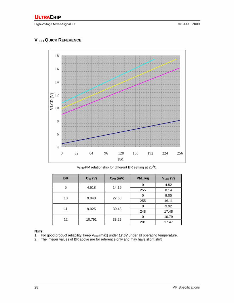
VLCD GENERATION
VLCD may be supplied either by internal charge pump or by external power supply. The source of VLCD is controlled by PC[3:2]. For good product reliability, it is recommended to keep VLCD under 17.5V over the entire operating range.
When VLCD is generated internally, the voltage level of VLCD is determined by three control registers: BR (Bias Ratio), PM (Potentiometer), and TC (Temperature Compensation), with the following relationship:
%))25(1()( 0 TPMVLCD CTPMCCV ×−+××+=
where CV0 and CPM are two constants, whose value
depends on the BR register setting. The values are provided in the table in the next page,
PM is the numerical value of PM register,
T is the ambient temperature in OC, and
CT is the temperature compensation coefficient as selected by TC register.
VLCD FINE TUNING
Gray shade and color STN LCD is sensitive to even a 1% mismatch between IC driving voltage and the VOP of LCD. However, it is difficult for LCD makers to guarantee such high precision matching of parts from different venders. It is therefore necessary to adjust VLCD to match the actual VOP of the LCD.
For best result, software or MTP based VLCD adjustment is the recommended method for VLCD fine-tuning. System designers should always consider the contrast fine tuning requirement before finalizing on the LCM design.
LOAD DRIVING STRENGTH
The power supply circuits of UC1611s are designed to handle LCD panels with load capacitance up to 40nF at VLCD=17V when VDD2 = 2.8V. For larger LCD panels or higher VLCD, use higher VDD2/3.
UUUULTRALTRALTRALTRACCCCHIPHIPHIPHIP
High-Voltage Mixed-Signal IC ©1999 ~ 2009
28 MP Specifications
VLCD QUICK REFERENCE
4
6
8
10
12
14
16
18
0 32 64 96 128 160 192 224 256
PM
VL
CD
(V
)
VLCD-PM relationship for different BR setting at 25oC.
BR CV0 (V) CPM (mV) PM_reg VLCD (V)
0 4.52 5 4.518 14.19
255 8.14
0 9.05 10 9.048 27.68
255 16.11
0 9.92 11 9.925 30.48
248 17.48
0 10.79 12 10.791 33.25
201 17.47
NOTE: 1. For good product reliability, keep VLCD (max) under 17.5V under all operating temperature. 2. The integer values of BR above are for reference only and may have slight shift.

UC1611S 160x256/16S Matrix LCD Controller-Driver
Revision A1.43 29
HI-V GENERATOR AND BIAS REFERENCE CIRCUIT
VDD2
CL
VB0+
RL
CB1
VDD2/VDD3
VB1+
VA1-
VB1-
VA1+
CA1
VDD
VSS2
VA0+
(OPTIONAL)
VDD
CA0
VLCDOUTVLCDIN
VDD3CB0
VB0-
VA0-
VSS
UC1611s
FIGURE 1: Reference circuit using internal Hi-V generator circuit
Note • Recommended component values: CA, CB: 100~250 x LCD load capacitance or 5µF (5V), whichever is higher. CL: 0.1µF ~0.5µF (25V) is appropriate for most applications. RL: 3.3M ~ 10MΩ Acts as a draining circuit when the power is abnormally shut down.

UUUULTRALTRALTRALTRACCCCHIPHIPHIPHIP
High-Voltage Mixed-Signal IC ©1999 ~ 2009
30 MP Specifications
LCD DISPLAY CONTROLS
CLOCK & TIMING GENERATOR
UC1611s contains a built-in system clock. All required components for the clock oscillator are built-in. No external parts are required.
Eight different line rates are provided for system design flexibility. The line rate is controlled by register LC[5:4]. When Mux-Rate is above 108, frame rate is calculated as:
Frame rate = Line-Rate / Mux-Rate.
When Mux-Rate is under 107, 80, 53, 40, Line rate will automatically be scaled down by 1.5, 2, 3, 4 respectively to reduce power consumption.
Flicker-free frame rate is dependent on LC material and gray-shade modulation scheme. Frame rate 150Hz is recommended for 16-shade mode. Choose lower frame rate for lower power, and choose higher frame rate to improve LCD contrast and minimize flicker.
DRIVER MODES
COM and SEG drivers can be in either Idle mode or Active mode, controlled by Display Enable flag (DC[2]). When SEG drivers are in idle mode, they will be connected together to ensure zero DC condition on the LCD.
DRIVER ARRANGEMENTS
The naming conventions are: COM(x), where x = 1~160, refers to the COM driver for the x-th row of pixels on the LCD panel. The mapping of COM(x) to LCD pixel rows is fixed and it is not affected by SL, CST, CEN, DST, DEN, MX or MY settings.
DISPLAY CONTROLS
There are three groups of display control flags in the control register DC: Driver Enable (DE), All-Pixel-ON (APO), and Inverse (PXV). DE has the overriding effect over PXV and APO.
DRIVER ENABLE (DE)
Driver Enable is controlled by the value of DC[2] via Set Display ON command. When DC[2] is set to OFF (logic “0”), both COM and SEG drivers will become idle and UC1611s will put itself into Sleep mode to conserve power.
When DC[2] is set to ON, the DE flag will become “1”, and UC1611s will first exit from Sleep mode, restore the power (VLCD, VD, etc.) and then turn on COM and DEG drivers.
ALL PIXELS ON (APO)
When set, this flag will force all active SEG drivers to output On signals, disregarding the data stored in the display buffer.
This flag has no effect when Display Enable is OFF and it has no effect on data stored in RAM.
INVERSE (PXV)
When this flag is set to ON, active SEG drivers will output the inverse of the value it received from the display buffer RAM. This flag has no impact on data stored in RAM.
PARTIAL SCROLL
The control register FL specifies a region of rows those are not affected by the SL register. Since SL register can be used to implement scroll function. The FL register can be used to implement fixed region when the other part of the display is scrolled by SL.
PARTIAL DISPLAY
UC1611s provides flexible control of Mux Rate and active display area. Please refer to command Set COM End, Set Partial Display Start, and Set Partial Display End for more detail.
GRAY-SHADE MODULATION MODE
UC1611s has two gray-shade modulation modes: 16-shade, 8-shade, 4-shade and On/Off mode.
The On/Off mode will consume roughly 40~45% less power than the 16-shade mode, and can be used for situations where power consumption is more critical than color fidelity.
Changing gray-shade modulation mode does not affect the content of SRAM display buffer, and the image data will remain the same after switching back and forth between On/Off mode and 16-shade mode.

UC1611S 160x256/16S Matrix LCD Controller-Driver
Revision A1.43 31
LAYOUT CONSIDERATIONS FOR COM SIGNALS
Under 16-gray-shade mode, the COM scanning pulses of UC1611s can be as short as 17µs. Since COM distortion can lead to reduction of effective duty factor of the LCM, it is critical to control the RC delay of COM signal to minimize distortion of COM scanning pulse. For the best image quality, limit the worst case RC delay of COM signal as calculated below.
RCCOM = (RROW / 3 + RCOM + ROUT) x CROW RCCOM-MAX 1.2µS
where CROW: LCD loading capacitance of one
row of pixels. It can be calculated by CLCD/Mux-Rate, where CLCD is the LCD panel capacitance.
RROW: ITO resistance over one row of pixels within the active area
RCOM: COM routing resistance from IC to the active area (COF+ITO routing)
ROUT: COM driver output impedance
In case RCCOM-MAX exceed the above constraint significantly, please make sure
| RCCOM-MAX – RCCOM-MIN | < 0.6µS
so that the COM scan pulse distortions from the top of the screen to the bottom of the screen are uniform.
For 8-gray-shade mode, the COM scanning pulse is about 35% slower than the 16-gray-shade mode. Therefore, the two constraints described above can be relaxed by 1/3 respectively to
RCCOM 1.6uS | RCCOM-MAX – RCCOM-MIN | < 0.8µS

UUUULTRALTRALTRALTRACCCCHIPHIPHIPHIP
High-Voltage Mixed-Signal IC ©1999 ~ 2009
32 MP Specifications
FIGURE 2: COM and SEG Driving Waveform
RAM W/R
POL
COM1
COM2
COM3
SEG1
SEG2
UC1611S 160x256/16S Matrix LCD Controller-Driver
Revision A1.43 33
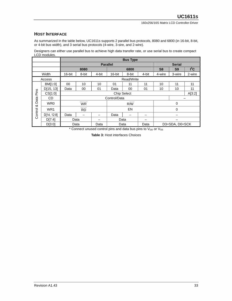
HOST INTERFACE As summarized in the table below, UC1611s supports 2 parallel bus protocols, 8080 and 6800 (in 16-bit, 8-bit, or 4-bit bus width), and 3 serial bus protocols (4-wire, 3-sire, and 2-wire).
Designers can either use parallel bus to achieve high data transfer rate, or use serial bus to create compact LCD modules.
Bus Type Parallel Serial 8080 6800 S8 S9 I2C
Width 16-bit 8-bit 4-bit 16-bit 8-bit 4-bit 4-wire 3-wire 2-wire
Access Read/Write BM[1:0] 00 10 10 01 11 11 10 11 11
D[15, 13] Data 00 01 Data 00 01 10 10 11 CS[1:0] Chip Select A[3:2]
CD Control/Data –
WR0 ___ __
WR _ _
R/W 0
WR1 ___ __
RD EN 0
D[14, 12:8] Data – – Data – – – D[7:4] Data – Data – – C
ontr
ol &
Dat
a P
ins
D[3:0] Data Data Data Data D3=SDA, D0=SCK * Connect unused control pins and data bus pins to VDD or VSS
Table 3: Host interfaces Choices

UUUULTRALTRALTRALTRACCCCHIPHIPHIPHIP
High-Voltage Mixed-Signal IC ©1999 ~ 2009
34 MP Specifications
PARALLEL INTERFACE
The timing relationship between UC1611s’ internal control signals, RD and WR, and their associated bus actions are shown in the figure below.
The Display RAM Read Interface is implemented as a two-stage pipe-line. This architecture requires a dummy read cycle to be performed before the actual data can propagate through the pipe-line and be read from data port D[7:0], every time memory address is modified (in 16-bit, 8-bit, or 4-bit mode) by either Set CA, or Set PA command.
There is no pipeline in write interface of Display RAM. Data is transferred directly from bus buffer to internal RAM on the rising edges of write pulses. 16-BIT, 8-BIT & 4-BIT BUS OPERATION
UC1611s supports 16-bit, 8-bit, and 4-bit bus widths. The bus width is determined by pins BM[1:0] and D15, D13.
UC1611s SARM read/write is based on 8-bit.
8-bit bus operation exactly doubles the clock cycles of 16-bit bus operation, while 4-bit doubles the clock cycles of 8-bit, MSB followed by LSB, including the dummy read, which also requires two clock cycles. For 16-bit bus operation, SRAM will perform read/write twice successively to finish a complete Read/Write.
LLSB DL DL+K CMSB CLSB Dummy DC DC+1 MMSB MLSB
L L+K L+K+1 C C+1 C+2 C+3 M
DL DL+K Dummy DC DC+1 DC+2
External CD ___ WR __ RD
D[15:0]
Internal Write
Read
Data Latch
Column Address
FIGURE 3.a: 16-bit Parallel Interface & Related Internal Signals
LLSB DL DL+K CMSB CLSB Dummy DC DC+1 MMSB MLSB
L L+K L+K+1 C C+1 C+2 C+3 M
DL DL+K Dummy DC DC+1 DC+2
External CD ___ WR __ RD
D[7:0]
Internal Write
Read
Data Latch
Column Address
FIGURE 3.b: 8-bit Parallel Interface & Related Internal Signals

UC1611S 160x256/16S Matrix LCD Controller-Driver
Revision A1.43 35
SERIAL INTERFACE
UC1611s supports 3 serial modes, 4-wire SPI mode (S8), 3-wire SPI mode (S9), and 2-wire SPI mode (I2C). Bus interface mode is determined by the wiring of the BM[1:0] and D7. See configuration table in the beginning of this section for more detail.
4-WIRE SERIAL INTERFACE (S8)
Pins CS[1:0] are used for chip select and bus cycle reset. Pin CD is used to determine the content of the data been transferred. During each write cycle, 8 bits of data, MSB first, are latched on eight rising SCK edges into an 8-bit data holder.
If CD=0, the data byte will be decoded as command. If CD=1, this 8-bit will be treated as data and transferred to proper address in the Display Data RAM on the rising edge of the last SCK pulse. Pin CD is examined when SCK is pulled low for the LSB (D0) of each token.
D7 D6 D5 D4 D3 D2 D1 D0
D7 D6 D5 D4 D3 D2 D1 D0
CS0
SDA
SCK
CD
Display Module
Read Command Read Status
MCU Data Display Module Data Transmission Starts Transmission Starts
FIGURE 4.a: 4-wire Serial Interface (S8) – Read
CS1/0
SDA
SCK
CD
D7 D6 D5 D4 D3 D2 D1 D0 D7 D6 D5
FIGURE 4.b: 4-wire Serial Interface (S8) – Write

UUUULTRALTRALTRALTRACCCCHIPHIPHIPHIP
High-Voltage Mixed-Signal IC ©1999 ~ 2009
36 MP Specifications
3-WIER SERIAL INTERFACE (S9)
Pins CS[1:0] are used for chip select and bus cycle reset. On each write cycle, the first bit is CD, which determines the content of the following 8 bits of data, MSB first. These 8 command or data bits are latched on rising SCK edges into an 8-bit data holder.
If CD=0, the data byte will be decoded as command.
If CD=1, this 8-bit will be treated as data and transferred to proper address in the Display Data RAM at the rising edge of the last SCK pulse. By sending CD information explicitly in the bit stream, control pin CD is not used, and should be connected to either VDD or VSS. The toggle of CS0 (or CS1) for each byte of data/command is recommended but optional.
CD D7 D6 D5 D4 D3 D2 D1 D0
D7 D6 D5 D4 D3 D2 D1 D0
CS0
SDA
SCK
Display Module
Read Command Read Status
MCU Data Display Module Data Transmission Starts Transmission Starts
FIGURE 5.a: 3-wire Serial Interface (S9) – Read
CS0
SDA
SCK
CD D7 D6 D5 D4 D3 D2 D1 D0 CD D7 D6
FIGURE 5.b: 3-wire Serial Interface (S9)

UC1611S 160x256/16S Matrix LCD Controller-Driver
Revision A1.43 37
I2C (2-WIRE) INTERFACE
Write Mode MPU MPU MPU MPU MPU ⇓ ⇑ ⇓ ⇓ ⇑ ⇓ ⇓ ⇑ ⇑ ⇓
S 0 1 1 1 A 3
A 2
C D
0 A D 7
D 0
A D7
… ... D0
A
A P
Read Mode MPU MPU MPU MPU MPU ⇓ ⇑ ⇑ ⇑ ⇓ ⇑ ⇑ ⇓ ⇓ ⇓
S 0 1 1 1 A 3
A 2
C D
1 A D 7
D 0
A D7
… ... D0
A
N P
When BM[1:0] is set to “LH” and D[7:6] is set to “HH”, UC1611s is configured as an I2C bus signaling protocol compliant slave device. Please refer to I2C standard for details of the bus signaling protocol, and AC Characteristic section for timing parameters of UltraChip implementation.
In this mode, pins CS[1:0] become A[3:2] and are used to configure UC1611s’ device address. Proper wiring to VDD or VSS is required for the IC to operate properly for I2C mode.
Each UC1611s I2C interface sequence starts with a “S” (Start) from the bus master, followed by a sequence header, containing a device address, the mode of transfer (CD, 0:Control, 1:Data), and the direction of the transfer (RW, 0:Write, 1:Read).
Since both WR and CD are expressed explicitly in the header byte, the control pins WR[1:0] and CD are not used in I2C mode and should be connected to VSS. The direction (read or write) and content type (command or data) of the data bytes following each header byte are fixed for the sequence. To change the direction (RW) or the content type (CD), start a new sequence with a START (S) flag, followed by a new header.
After receiving the header, the UC1611s will send out a “A” (Acknowledge signal). Then, depends on the setting of the header, the transmitting device (either the bus master or UC1611s) will start placing data bits on SDA, MSB to LSB, and the sequence will repeat until a STOP signal (P, in WRITE mode), or an N (Not Acknowledged, in READ mode) is sent by the bus master.
When using I2C serial mode, if command System Reset is to be written, the writing sequence must be finished (STOP) before succeeding data or commands start. The flow chart on the right shows a writing sequence with a “System Reset” command.
Note that, for data read (CD=1), the first byte of data transmitted will be dummy.
START
Header
STOP
START
Header
Command / Data
STOP
Command = System Reset
Command / Data
Command / Data

UUUULTRALTRALTRALTRACCCCHIPHIPHIPHIP
High-Voltage Mixed-Signal IC ©1999 ~ 2009
38 MP Specifications
HOST INTERFACE REFERENCE CIRCUIT
RST
VSS
VDD
D15~D0 DB15~DB0
RD
VDD
GND
CS1
WR0(WR)
BM0
CD CD
VCC
ID1
UC1611s
WR1(RD)
MPUDECODER
CS0
BM1
WR
IORQ
VDD
ADDRESS
FIGURE 6: 8080/16-bit parallel mode reference circuit
DECODER
MPU
VDD
DB7 ~ DB0
CD
CS1
CD
WR1(RD)
RST
DB15
VDD
VCC
WR0(WR)RD
ADDRESS
DB7~DB0
UC1611s
GND
IORQ
WR
BM1
VDD
CS0
VDD
DB13
ID1
BM0
VSS
FIGURE 7: 8080/8-bit parallel mode reference circuit

UC1611S 160x256/16S Matrix LCD Controller-Driver
Revision A1.43 39
CD
BM0
VDD
CS1
WR1(RD)
VDD
D15
VDD
CD
MPU
D13
GND
CS0
D3-D0
VDD
RD
VDD
IORQ
BM1
UC1611s
WR0(WR)
RST
VCC
D3-D0
WR
DECODER
VSS
ID1
ADDRESS
FIGURE 8: 8080/4-bit parallel mode reference circuit
ADDRESS
CDR/W
VCC
BM0
DB15~DB0
MPU
WR0(R/W)
DECODER
ID1
VSS
CS1
E
D15-D0
VDD
VDD
CD
BM1
WR1(E)
VDD
UC1611s
GND
RST
CS0
IORQ
VDD
FIGURE 9: 6800/16-bit parallel mode reference circuit
UUUULTRALTRALTRALTRACCCCHIPHIPHIPHIP
High-Voltage Mixed-Signal IC ©1999 ~ 2009
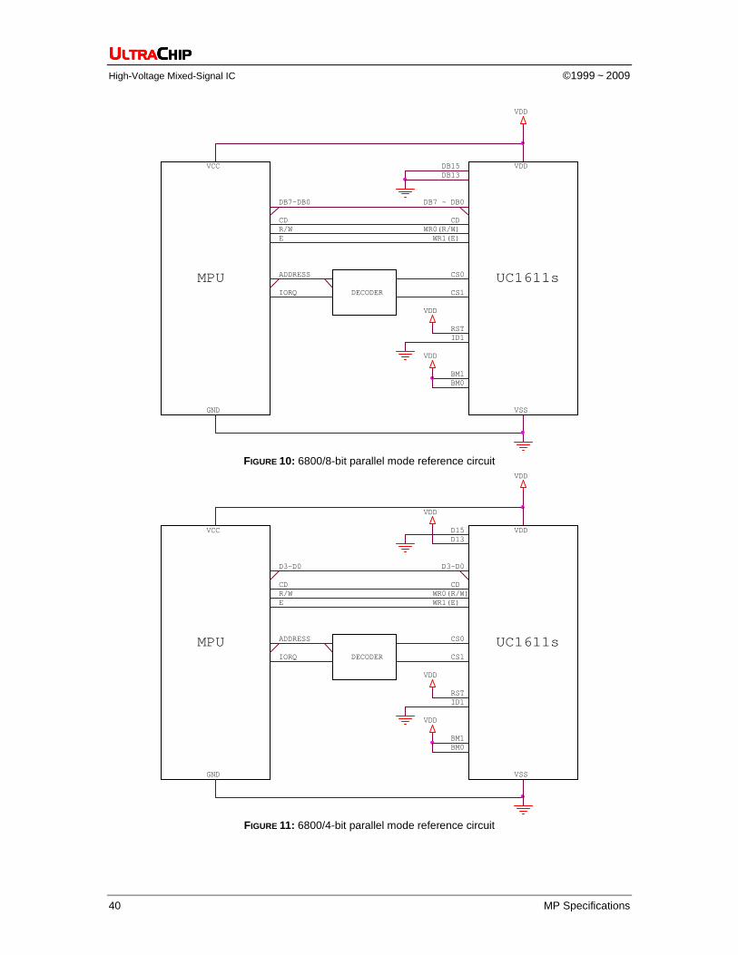
40 MP Specifications
CD
BM0
VDD
DB13
UC1611sDECODER
VSS
VCC
ID1RST
ADDRESSMPU
WR1(E)
GND
BM1
WR0(R/W)
VDD
R/W
CS0
E
VDD
DB7 ~ DB0
CS1
VDD
IORQ
CD
DB15
DB7-DB0
FIGURE 10: 6800/8-bit parallel mode reference circuit
VSS
CS1
CS0
VCC
MPU
RST
D3-D0
IORQ
ADDRESS
WR0(R/W)
GND
ID1
D13
WR1(E)
VDD
BM0
CD
D15
VDD
R/W
VDD
VDD
UC1611s
VDD
DECODER
BM1
D3-D0
CD
E
FIGURE 11: 6800/4-bit parallel mode reference circuit

UC1611S 160x256/16S Matrix LCD Controller-Driver
Revision A1.43 41
VDD
SDA(DB3)CD
VDD
BM1
DB13
UC1611s
SCK(DB0)
GND
BM0
DECODER
VCC
VDD
IORQ
VDD
ADDRESS
ID1
WR0CD
RST
WR1
MPUCS1
SDASCK
CS0
DB15
VSS
FIGURE 12: 4-Wire SPI (S8) serial mode reference circuit
DB15
ADDRESS
RST
GND
VDD
CS1
VCC
VDD
DB13
CDSDA SDA(DB3)
WR0
IORQ
CS0
ID1
SCK
VDD
UC1611s
WR1
VDD
MPUDECODER
BM1
VSS
SCK(DB0)
BM0
VDD
FIGURE 13: 3-Wire SPI (S9) serial mode reference circuit

UUUULTRALTRALTRALTRACCCCHIPHIPHIPHIP
High-Voltage Mixed-Signal IC ©1999 ~ 2009
42 MP Specifications
D13
UC1611s
WR1
SCK
VDD
MPU
VDD
SCK(D0)
VDD
CS0(A2)
SDA(D3)
WR0
RST
CD
D15R3
CS1(A3)
R2
VSS
SDA
BM1
VDD
BM0
ID1
GND
VDD
VCC
FIGURE 14: 2-Wire SPI (I2C) serial mode reference circuit
Note:
1. RST pin is optional. When RST pin is not used, connect the pin to VDD.
2. When using I2C serial mode, CS1/0 are user configurable and affect A[3:2] of device address.
3. R1, R2: 2k ~ 10k Ω. Use lower resistor for bus speed up to 3.6MHz; while use higher resistor for lower power.

UC1611S 160x256/16S Matrix LCD Controller-Driver
Revision A1.43 43
DISPLAY DATA RAM
DATA ORGANIZATION
The display data is 4-bit per pixel and stored in a dual port SRAM. The SRAM is organized as 160x 256x4.
After setting CA and PA, the next data write cycle will store the data for the specified pixel to the proper memory location.
Please refer to the map in the following page for the relation between the COM, SEG, SRAM, and various memory control registers.
DISPLAY DATA RAM ACCESS
The Display RAM is a special purpose dual port RAM that allows asynchronous access to both its column and row data. Thus, RAM can be independently accessed both for Host Interface and for display operations.
DISPLAY DATA RAM ADDRESSING
A Host Interface (HI) memory access operation starts with specifying Page Address (PA) and Column Address (CA) by issuing Set Page Address and Set Column Address commands.
If wrap-around (WA, AC[0]) is OFF (0), CA will stop incrementing after reaching the end of page (MC), and system programmers need to set the values of PA and CA explicitly.
If WA is ON (1), when CA reaches end of page, CA will be reset to 0 and PA will increment or decrement, depending on the setting of Page Increment Direction (PID, AC[2]). When PA reaches the boundary of RAM (i.e. PA = 0 or 79), PA will be wrapped around to the other end of RAM and continue.
MX IMPLEMENTATION
Column Mirroring (MX) is implemented by selecting either (CA) or (255–CA) as the RAM column address. Changing MX affects the data written to the RAM.
Since MX has no effect of the data already stored in RAM, changing MX does not have immediate effect on the displayed pattern. To refresh the display, refresh the data stored in RAM after setting MX.
RAM ADDRESS GENERATION
The mapping of the data store in the display SRAM and the scanning electrodes can be obtained by combining the fixed COM scanning sequence and the following RAM address generation formula.
When FL=0, during the display operation, the RAM line address generation can be mathematically represented as following:
For the 1st line period of each field Line = SL
Otherwise Line = Mod (Line + 1, 160)
Where Mod is the modular operator, and Line is the bit slice line address of RAM to be outputted to SEG drivers. Line 0 corresponds to the first bit-slice of data in RAM.
The above Line generation formula produces the “loop around” effect as it effectively resets Line to 0 when Line+1 reaches 160. Effects such as page scrolling and page swapping can be emulated by changing SL dynamically.
MY IMPLEMENTATION
Row Mirroring (MY) is implemented by reversing the mapping order between COM electrodes and RAM, i.e. the mathematical address generation formula becomes:
For the 1st line period of each field Line = Mod(SL + MUX - 1, 160)
where MUX is the Mux rate Otherwise
Line = Mod( Line - 1 , 160)
Visually, the effect of MY is equivalent to flipping the display upside down. The data stored in display RAM is not affected by MY.

UUUULTRALTRALTRALTRACCCCHIPHIPHIPHIP
High-Voltage Mixed-Signal IC ©1999 ~ 2009
44 MP Specifications
WINDOW PROGRAM Window program is designed for data write in a specified window range of SRAM address. The procedure should start with window boundary registers setting (WPP0, WPP1, WPC0 and WPC1) and then enable AC[3]. After AC[3] is set, data can be written to SRAM within the window address range which is specified by (WPP0, WPC0) and (WPP1, WPC1). AC[3] should be cleared after any modification of window boundary registers and then set again in order to initialize another window program.
The data write direction will be determined by AC[2:0] and MX settings. When AC[0]=1, the data write can be consecutive within the range of the specified window. AC[1] will control the data write in either column or row direction. AC[2] will result the data write starting either from row WPP0 or WPP1. MX is for the initial column address either from WPC0 to WPC1 or from (MC-WPC0 to MC-WPC1).
Example1: AC[2:0] = 001, MX=0 (PA auto INCREASING, COLUMN increasing first, auto wrap around, Mirror-X OFF) 0 255 (column) 0 159 (row) Example 2: AC[2:0] = 111, MX = 0 (PA auto DESCREASING, PAGE increasing first, auto wrap around, Mirror-X OFF) 0 255 (column) 0 159 (row)
(WPP0, WPC0)
(WPP1,WPC1)
(WPP0, WPC0)
(WPP1,WPC1)

UC1611S 160x256/16S Matrix LCD Controller-Driver
Revision A1.43 45
Line RAM0 1 Adderss SL=0 SL=16 SL=0 SL=16
D3/0 D7/4 00H COM1 COM145 COM160 COM16D7/4 D3/0 01H COM2 COM146 COM159 COM15D3/0 D7/4 02H COM3 COM147 COM158 COM14D7/4 D3/0 03H COM4 COM148 COM157 COM13D3/0 D7/4 04H COM5 COM149 COM156 COM12D7/4 D3/0 05H COM6 COM150 COM155 COM11D3/0 D7/4 06H COM7 COM151 COM154 COM10D7/4 D3/0 07H COM8 COM152 COM153 COM9D3/0 D7/4 08H COM9 COM153 COM152 COM8D7/4 D3/0 09H COM10 COM154 COM151 COM7D3/0 D7/4 0AH COM11 COM155 COM150 COM6D7/4 D3/0 0BH COM12 COM156 COM149 COM5D3/0 D7/4 0CH COM13 COM157 COM148 COM4D7/4 D3/0 0DH COM14 COM158 COM147 COM3D3/0 D7/4 0EH COM15 COM159 COM146 COM2D7/4 D3/0 0FH COM16 COM160 COM145 COM1D3/0 D7/4 10H COM17 COM1 COM144 COM160D7/4 D3/0 11H COM18 COM2 COM143 COM159D3/0 D7/4 12H COM19 COM3 COM142 COM158D7/4 D3/0 13H COM20 COM4 COM141 COM157D3/0 D7/4 14H COM21 COM5 COM140 COM156D7/4 D3/0 15H COM22 COM6 COM139 COM155D3/0 D7/4 16H COM23 COM7 COM138 COM154D7/4 D3/0 17H COM24 COM8 COM137 COM153D3/0 D7/4 18H COM25 COM9 COM136 COM152D7/4 D3/0 19H COM26 COM10 COM135 COM151D3/0 D7/4 1AH COM27 COM11 COM134 COM150D7/4 D3/0 1BH COM28 COM12 COM133 COM149D3/0 D7/4 1CH COM29 COM13 COM132 COM148D7/4 D3/0 1DH COM30 COM14 COM131 COM147D3/0 D7/4 1EH COM31 COM15 COM130 COM146D7/4 D3/0 1FH COM32 COM16 COM129 COM145
D3/0 D7/4 8CH COM141 COM125 COM20 COM36D7/4 D3/0 8DH COM142 COM126 COM19 COM35D3/0 D7/4 8EH COM143 COM127 COM18 COM34D7/4 D3/0 8FH COM144 COM128 COM17 COM33D3/0 D7/4 90H COM145 COM129 COM16 COM32D7/4 D3/0 91H COM146 COM130 COM15 COM31D3/0 D7/4 92H COM147 COM131 COM14 COM30D7/4 D3/0 93H COM148 COM132 COM13 COM29D3/0 D7/4 94H COM149 COM133 COM12 COM28D7/4 D3/0 95H COM150 COM134 COM11 COM27D3/0 D7/4 96H COM151 COM135 COM10 COM26D7/4 D3/0 97H COM152 COM136 COM9 COM25D3/0 D7/4 98H COM153 COM137 COM8 COM24D7/4 D3/0 99H COM154 COM138 COM7 COM23D3/0 D7/4 9AH COM155 COM139 COM6 COM22D7/4 D3/0 9BH COM156 COM140 COM5 COM21D3/0 D7/4 9CH COM157 COM141 COM4 COM20D7/4 D3/0 9DH COM158 COM142 COM3 COM19D3/0 D7/4 9EH COM159 COM143 COM2 COM18D7/4 D3/0 9FH COM160 COM144 COM1 COM17
0
SE
G1
SE
G2
SE
G3
SE
G4
SE
G5
SE
G6
SE
G7
SE
G8
SEG
252
SEG
253
SEG
254
SE
G25
5
SEG
256
1
SE
G25
6
SE
G25
5
SE
G25
4
SE
G25
3
SE
G25
2
SE
G25
1
SE
G25
0
SE
G24
9
SE
G5
SE
G4
SE
G3
SE
G2
SE
G1
Page 4
Page 3
Page 78
Page 79
Page 74
Page 75
Page 76
Page 77
Page 8
Page 7
Page 6
Page 5
MSF
MX
Page 15
Page 14
Page 73
Page 9
Page 71
Page 70
Page 72
Page 13
Page 12
Page 11
Page 10
MY=1MY=0
Page 2
Page 1
Page 0
When DC[5:3] = 0xxb :
Example for memory mapping: let MX = 0, MY = 0, SL = 0, MSF = 0, according to the data shown in the above table: ⇒ Page 0 SEG 1 : ( D[7:0] ) 0000 1111 b ⇒ Page 0 SEG 2 : ( D[7:0] ) 1111 0000 b

UUUULTRALTRALTRALTRACCCCHIPHIPHIPHIP
High-Voltage Mixed-Signal IC ©1999 ~ 2009
46 MP Specifications
Line RAM0 1 Adderss SL=0 SL=16 SL=0 SL=16
D0 D4 00H COM1 COM145 COM160 COM16D1 D5 01H COM2 COM146 COM159 COM15D2 D6 02H COM3 COM147 COM158 COM14D3 D7 03H COM4 COM148 COM157 COM13D4 D0 04H COM5 COM149 COM156 COM12D5 D1 05H COM6 COM150 COM155 COM11D6 D2 06H COM7 COM151 COM154 COM10D7 D3 07H COM8 COM152 COM153 COM9D0 D4 08H COM9 COM153 COM152 COM8D1 D5 09H COM10 COM154 COM151 COM7D2 D6 0AH COM11 COM155 COM150 COM6D3 D7 0BH COM12 COM156 COM149 COM5D4 D0 0CH COM13 COM157 COM148 COM4D5 D1 0DH COM14 COM158 COM147 COM3D6 D2 0EH COM15 COM159 COM146 COM2D7 D3 0FH COM16 COM160 COM145 COM1D0 D4 10H COM17 COM1 COM144 COM160D1 D5 11H COM18 COM2 COM143 COM159D2 D6 12H COM19 COM3 COM142 COM158D3 D7 13H COM20 COM4 COM141 COM157D4 D0 14H COM21 COM5 COM140 COM156D5 D1 15H COM22 COM6 COM139 COM155D6 D2 16H COM23 COM7 COM138 COM154D7 D3 17H COM24 COM8 COM137 COM153D0 D4 18H COM25 COM9 COM136 COM152D1 D5 19H COM26 COM10 COM135 COM151D2 D6 1AH COM27 COM11 COM134 COM150D3 D7 1BH COM28 COM12 COM133 COM149D4 D0 1CH COM29 COM13 COM132 COM148D5 D1 1DH COM30 COM14 COM131 COM147D6 D2 1EH COM31 COM15 COM130 COM146D7 D3 1FH COM32 COM16 COM129 COM145
D0 D4 90H COM145 COM129 COM16 COM32D1 D5 91H COM146 COM130 COM15 COM31D2 D6 92H COM147 COM131 COM14 COM30D3 D7 93H COM148 COM132 COM13 COM29D4 D0 94H COM149 COM133 COM12 COM28D5 D1 95H COM150 COM134 COM11 COM27D6 D2 96H COM151 COM135 COM10 COM26D7 D3 97H COM152 COM136 COM9 COM25D0 D4 98H COM153 COM137 COM8 COM24D1 D5 99H COM154 COM138 COM7 COM23D2 D6 9AH COM155 COM139 COM6 COM22D3 D7 9BH COM156 COM140 COM5 COM21D4 D0 9CH COM157 COM141 COM4 COM20D5 D1 9DH COM158 COM142 COM3 COM19D6 D2 9EH COM159 COM143 COM2 COM18D7 D3 9FH COM160 COM144 COM1 COM17
0
SE
G1
SE
G2
SE
G3
SE
G4
SE
G5
SE
G6
SE
G7
SE
G8
SEG
252
SEG
253
SEG
254
SE
G25
5
SEG
256
1
SE
G25
6
SE
G25
5
SE
G25
4
SE
G25
3
SE
G25
2
SE
G25
1
SE
G25
0
SE
G24
9
SE
G5
SE
G4
SE
G3
SE
G2
SE
G1
MSF
Page 0
Page 1
MX
Page 3
Page 19
Page 18
Page 2
MY=1MY=0
When DC[5:3]=100b :
Example for memory mapping: Let MX = 0, MY = 0, SL = 0, MSF = 0, according to the data shown in the above table:
⇒ Page 0 SEG 1 : ( D[7:0] ) 1000 1111 b ⇒ Page 0 SEG 2 : ( D[7:0] ) 0100 1100 b

UC1611S 160x256/16S Matrix LCD Controller-Driver
Revision A1.43 47
RESET & POWER MANAGEMENT
TYPES OF RESET
UC1611s has two different types of Reset: Power-ON-Reset and System-Reset.
Power-ON-Reset is performed right after VDD is connected to power. Power-On-Reset will first wait for about 5~10mS, depending on the time required for VDD to stabilize, and then trigger the System Reset.
System Reset can also be activated by software command or by connecting RST pin to ground.
In the following discussions, Reset means System Reset.
RESET STATUS
When UC1611s enters RESET sequence:
• Operation mode will be “Reset”
• All control registers are reset to default values. Refer to Control Registers for details of their default values.
OPERATION MODES
UC1611s has 3 operating modes (OM): Reset, Normal, Sleep.
Mode Reset Sleep Normal
OM 00 10 11
Host Interface Active Active Active
Clock OFF OFF ON
LCD Drivers OFF OFF ON
Charge Pump OFF OFF ON
Draining Circuit ON ON OFF
Table 4: Operating Modes
CHANGING OPERATION MODE
In addition to Power-ON-Reset, two commands will initiate OM transitions:
Set Display Enable, and System Reset.
When DC[2] is modified by Set Display Enable, OM will be updated automatically. There is no other action required to enter Sleep mode.
OM changes are synchronized with the edges of the IC’s internal clock. To ensure consistent system states, wait at least 10µS after Set Display Enable or System Reset command.
Action Mode OM
Reset command RST_ pin pulled “L” Power-ON-Reset
Reset 00
Set Driver Enable to “0” Sleep 10
Set Driver Enable to “1” Normal 11
Table 5: OM changes
Both Reset mode and Sleep mode drain the charges stored in the external capacitors CB0, CB1, and CL. When entering Reset mode or Sleep mode, the display drivers will be disabled.
The difference between Sleep mode and Reset mode is that, Reset mode clears all control registers and restores them to default values, while Sleep mode retains all the control registers values set by the user.
It is recommended to use Sleep Mode for Display OFF operations as the IC consumes very little energy in Sleep mode (typically under 1µA).
EXITING SLEEP MODE
UC1611s contains internal logic to check whether VLCD are ready before releasing COM and SEG drivers from their idle states. When exiting Sleep or Reset Mode, COM and SEG drivers will not be activated until UC1611s’ internal voltage sources are restored to their proper values.

UUUULTRALTRALTRALTRACCCCHIPHIPHIPHIP
High-Voltage Mixed-Signal IC ©1999 ~ 2009
48 MP Specifications
POWER-UP SEQUENCE
UC1611s power-up sequence is simplified by built-in “Power Ready” flags and the automatic invocation of System-Reset command after Power-ON-Reset.
System programmers are only required to wait 150 mS before the CPU starting to issue commands to UC1611s. No additional time sequences are required between enabling the charge pump, turning on the display drivers, writing to RAM or any other commands.
There’s no delay needed while turning on VDD and VDD2/3, and either one can be turned on first.
FIGURE 15: Reference Power-Up Sequence
POWER-DOWN SEQUENCE
To prevent the charge stored in capacitor CL from causing abnormal residue horizontal line on display when VDD is switched off, use Reset mode to enable the built-in charge draining circuit to discharge the external capacitor.
When internal VLCD is not used, UC1611s will NOT drain VLCD during RESET. System designers need to make sure external VLCD source is properly drained off before turning off VDD.
FIGURE 16: Reference Power-Down Sequence
Figure 17: Delay allowance between VDD and VDD2/3
MTP version
Turn on the power
Set LCD Bias Ratio (BR) Set Potential Meter (PM)
Set Display Enable
Set RST Low
Wait 1mS
Set RST High
Wait for MTP-Read 150 mS
10µS < T1< 10 mS Tf < 10 mS
VDD2/3 ≥ 2.5V
VDD ≥ 1.8V
VDD2/3 ≥ VDD
Either VDD or VDD2/3 may be turned on first.
TWait > 10mS VDD < 0.1V
Reset command
Turn OFF the power
Wait ~1 mS

UC1611S 160x256/16S Matrix LCD Controller-Driver
Revision A1.43 49
MULTI-TIME PROGRAM NV MEMORY
OVERVIEW
MTP feature is available for UC1611s such that LCM maker can record an PM offset value in non-volatile memory cells, which can then be used to adjust the effective VLCD value, in order to achieve high level of consistency for LCM contrast across all shipments.
To accomplish this purpose, three operations are supported by UC1611s: MTP-Erase, MTP-Program, MTP-Read.
MTP-Program requires an external power source supplied to TST4 pin. MTP allows to program at least 10 times and should be performed only by the LCM makers.
MTP-Read is facilitated by the internal DC-DC converter built-in on UC1611s, no external power source is required, and it is performed automatically after hardware RESET (power-ON or pin RESET).
OPERATION FOR THE SYSTEM USERS
For the MTP version of UC1611s, the content of the NV memory will be read automatically after the power-on and hardware pin RESET. There is no user intervention or external power source required. When set up properly, the VLCD will be fine tuned to achieve high level of consistency for the LCM contrast.
The MTP-READ is a relatively slow process and the time required can vary quite a bit. For a successful MTP-READ operation, the MS and WS bits in the Read Status commands will exhibit the following waveforms.
As illustrated above, the MS, WS will go through a 0,01,01,10,1 transition. When the MS, WS=0,1 state is reached, it means the LCM is ready to be turned on.
During the MTP-READ process, it is actually safe to issue commands or perform data write to the LCM. The only thing that is blocked is the LSB of the Set Display Enable command, which results in the DC[2] being effectively locked at “0” during this auto-MTP-READ process.
Although user can use Read Status command in a polling loop to make sure MS,WS=0,1 before proceeding with the Set Display Enable command, however, it may be simpler to just issue the Set Display Enable command every 0.2~2 second, repeatedly, together with other LCM optimization settings, such as BR, CEN, TC, etc.
The above “Periodical re-initializing” approach is also an effective safeguard against accidental display off events such as
• ESD strikes
• Mechanical shocks causing LCM connector to malfunction temporarily
HARDWARE VS. SOFTWARE RESET
The auto-MTP-READ is only performed for hardware RESET (power-ON and RST pin), but not for software RESET command. This enables the ICs to turn on display faster without the delay caused by MTP-READ.
It is recommended to use software RESET for normal operation control purpose and hardware RESET only during the event of power up and power down.
OPERATION FOR THE LCM MAKERS
Always ERASE the MTP NV memory cells, before starting the Write process.
RST
150 mS
MS
WS
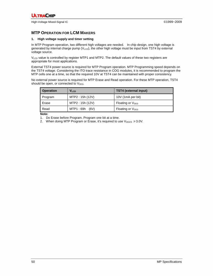
UUUULTRALTRALTRALTRACCCCHIPHIPHIPHIP
High-Voltage Mixed-Signal IC ©1999~2009
50 MP Specifications
MTP OPERATION FOR LCM MAKERS 1. High voltage supply and timer setting
In MTP Program operation, two different high voltages are needed. In chip design, one high voltage is generated by internal charge pump (VLCD), the other high voltage must be input from TST4 by external voltage source.
VLCD value is controlled by register MTP1 and MTP2. The default values of these two registers are appropriate for most applications.
External TST4 power source is required for MTP Program operation. MTP Programming speed depends on the TST4 voltage. Considering the ITO trace resistance in COG modules, it is recommended to program the MTP cells one at a time, so that the required 10V at TST4 can be maintained with proper consistency.
No external power source is required for MTP Erase and Read operation. For these MTP operation, TST4 should be open, or connected to VDD3.
Operation VLCD TST4 (external input)
Program MTP2 : 15h (12V) 10V (1mA per bit)
Erase MTP2 : 15h (12V) Floating or VDD3
Read MTP1 : 69h (6V) Floating or VDD3
Note: 1. Do Erase before Program. Program one bit at a time. 2. When doing MTP Program or Erase, it’s required to use VDD2/3 3.0V.

UC1611S 160x256/16S Matrix LCD Controller-Driver
Revision A1.43 51
2. Read MTP status bits
With normal Get Status method (CD=0,W/R=1), MTP operation status can be monitored in the real time. There are 3 status bits (WS, MD, MS) in status register. MTP control circuit will read to verify if the operation (program, erase) success or not. If the operation succeeded, and current operation will be ended with WS=1. If it failed, last operation will be automatically retried two more times. If it fails 3 times, WS will be set to 0 and the operation is aborted. MD is MTP ID, which is either 1 for MTP IC. No transition.
MTP CELL VALUE USAGE
There are 6 MTP cell bits.
PMO[5:0] : VLCD Trim When PMO[5]=1: PM with trim = PM - PMO[4:0] When PMO[5]=0: PM with trim = PM + PMO[4:0]
MTP status bits, TST4 & VLCD Waveform
WS
MD
MS
Program/Erase
VLCD=12V Read to verify
VLCD=6V
VLCD
MTP Command
Erase VDD3
TST4
Program 10V
may repeat 3 times

UUUULTRALTRALTRALTRACCCCHIPHIPHIPHIP
High-Voltage Mixed-Signal IC ©1999~2009
52 MP Specifications
MTP COMMAND SEQUENCE SAMPLE CODES
The following tables are examples of command sequence for MTP Program and Erase operations. These are only to demonstrate some “typical, generic” scenarios. Designers are encouraged to study related sections of the datasheet and find out what the best parameters and control sequences are for their specific design needs.
MTP operations (Erase, Program, Read) and Set Display ON is mutual exclusive. There is no harm done to the IC or the LCM if this is violated. However, the violating commands will be ignored.
Type Required: These items are required Customized: These items are not necessary if customer parameters are the same as default Advanced: We recommend new users to skip these commands and use default values. Optional: These commands depend on what users want to do.
C/D The type of the interface cycle. It can be either Command (0) or Data (1)
W/R The direction of dataflow of the cycle. It can be either Write (0) or Read (1).
(1) MTP Program Sample Code
Type C/D W/R D7 D6 D5 D4 D3 D2 D1 D0 Chip Action Comments
R – – – – – – – – – – Set RST pin Low Wait 1mS after RST is Low
R – – – – – – – – – – Set RST pin High
R – – – – – – – – – – Automatic Power-ON Reset.
Wait ~150mS
R 0 0 1 0 1 0 0 0 1 1 Set Line Rate Set LC[5:4]=11b
R 0 0 1 1 1 1 0 1 0 0 Set VMTP1 Potentiometer Set MTP VLCD
R 0 0 0 1 1 0 1 0 0 1 MTP1: 69h(6V)
R 0 0 1 1 1 1 0 1 0 1 Set VMTP2 Potentiometer Set MTP VLCD
R 0 0 0 0 1 0 0 1 0 1 MTP2: 25h(12V)
R 0 0 1 1 1 1 0 1 1 0 Set MTP Write Timer Set MTP Timer
R 0 0 0 0 1 0 0 1 0 1 MTP3:25h(100mS)
R 0 0 1 1 1 1 0 1 1 1 Set MTP Read Timer Set MTP Timer
R 0 0 0 0 0 0 0 1 0 1 MTP4:05h(10mS)
R 0 0 1 0 1 1 1 0 0 1 Set MTP Write Mask Set MTP Bit Mask
C 0 0 0 0 0 0 0 0 0 1 MTPM Ex: To program PMO[5:0],
set MTPM *
R - - - - - - - - - - Apply TST4 voltage Program: 10V
R 0 0 1 0 1 1 1 0 0 0 Set MTP Control Set MTPC[3]=1
R 0 0 - - 0 0 1 0 1 1 Set MTPC[2:0]=011
R 0 1 - - - - - ws - MS Get Status & PM Check MTP Status until MS=0 and WS=1
R Remove TST4 voltage
R VDD=0V Power OFF
* It is recommended that users program one bit at a time.
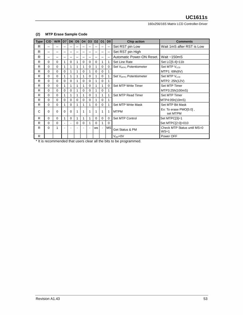
UC1611S 160x256/16S Matrix LCD Controller-Driver
Revision A1.43 53
(2) MTP Erase Sample Code
Type C/D W/R D7 D6 D5 D4 D3 D2 D1 D0 Chip action Comments
R – – – – – – – – – – Set RST pin Low Wait 1mS after RST is Low
R – – – – – – – – – – Set RST pin High
R – – – – – – – – – – Automatic Power-ON Reset. Wait ~150mS R 0 0 1 0 1 0 0 0 1 1 Set Line Rate Set LC[5:4]=11b
R 0 0 1 1 1 1 0 1 0 0 Set VMTP1 Potentiometer Set MTP VLCD
R 0 0 0 1 1 0 1 0 0 1 MTP1: 69h(6V)
R 0 0 1 1 1 1 0 1 0 1 Set VMTP2 Potentiometer Set MTP VLCD
R 0 0 0 0 1 0 0 1 0 1 MTP2: 25h(12V)
R 0 0 1 1 1 1 0 1 1 0 Set MTP Write Timer Set MTP Timer
R 0 0 0 0 1 0 0 1 0 1 MTP3:25h(100mS)
R 0 0 1 1 1 1 0 1 1 1 Set MTP Read Timer Set MTP Timer
R 0 0 0 0 0 0 0 1 0 1 MTP4:05h(10mS)
R 0 0 1 0 1 1 1 0 0 1 Set MTP Write Mask Set MTP Bit Mask
C 0 0 0 0 1 1 1 1 1 1 MTPM Ex: To erase PMO[5:0] ,
set MTPM
R 0 0 1 0 1 1 1 0 0 0 Set MTP Control Set MTPC[3]=1
R 0 0 - - 0 0 1 0 1 0 Set MTPC[2:0]=010
R 0 1 - - - - - ws - MS Get Status & PM Check MTP Status until MS=0 WS=1
R VDD=0V Power OFF
* It is recommended that users clear all the bits to be programmed.

UUUULTRALTRALTRALTRACCCCHIPHIPHIPHIP
High-Voltage Mixed-Signal IC ©1999~2009
54 MP Specifications
SAMPLE COMMAND SEQUENCES The following tables are examples of command sequence for power-up, power-down and display ON/OFF operations. These are only to demonstrate some “typical, generic” scenarios. Designers are encouraged to study related sections of the datasheet and find out what the best parameters and control sequences are for their specific design needs. Type Required: These items are required
Customized: These items are not necessary, if customer parameters are the same as default Advanced: We recommend new users to skip these commands and use default values. Optional: These commands depend on what users want to do.
C/D The type of the interface cycle. It can be either Command (0) or Data (1) W/R The direction of data-flow of the cycle. It can be either Write (0) or Read (1).
POWER-UP
Type C/D W/R D7 D6 D5 D4 D3 D2 D1 D0 Chip action Comments
R – – – – – – – – – – Turn on VDD and VDD2/3 Wait until VDD and VDD2/3 are stable
R – – – – – – – – – – Set RST pin Low Wait 1mS after RST is Low
R – – – – – – – – – – Set RST pin High
R – – – – – – – – – – Automatic Power-ON Reset. Wait ~150mS
C 0 0 0 0 1 0 0 1 # # Set Temp. Compensation
C 0 0 1 1 0 0 0 0 0 0
C 0 0 0 0 0 0 # # # # Set LCD Mapping Control
Set up LCD format specific parameters, MX, MY, etc.
A 0 0 1 0 1 0 0 0 # # Set Line Rate Fine tune for power, flicker, contrast, and shading.
C 0 0 1 1 1 0 1 0 # # Set LCD Bias Ratio
R 0 0
0 0
1 #
0 #
0 #
0 #
0 #
0 #
0 #
1 #
Set Gain and PM LCD specific operating voltage setting
O
1 . . 1
0 . . 0
# . . #
# . . #
# . . #
# . . #
# . . #
# . . #
# . . #
# . . #
Write display RAM Set up display image
R 0 0 1 0 1 0 1 1 1 1 Set Display Enable
POWER-DOWN
Type C/D W/R D7 D6 D5 D4 D3 D2 D1 D0 Chip action Comments
R 0 0 1 1 1 0 0 0 1 0 System Reset
R – – – – – – – – – – Draining capacitor Wait ~1mS before VDD OFF
DISPLAY-OFF
Type C/D W/R D7 D6 D5 D4 D3 D2 D1 D0 Chip action Comments
R 0 0 1 0 1 0 1 0 0 0 Set Display Disable
O 1 . . 1
0 . . 0
# . . #
# . . #
# . . #
# . . #
# . . #
# . . #
# . . #
# . . #
Write display RAM Set up display image. (Image update is optional. Data in the RAM is retained through the SLEEP state.)
R 0 0 1 0 1 0 1 1 1 1 Set Display Enable

UC1611S 160x256/16S Matrix LCD Controller-Driver
Revision A1.43 55
ESD CONSIDERATION 1. UC1600 series products usually are provided in bare die format to customers. This makes the product
particularly sensitive to ESD damage during handling and manufacturing process. It is therefore highly recommended that LCM makers strictly follow the "JESD 625-A Requirements for Handling Electrostatic-Discharge-Sensitive (ESDS) Devices" when manufacturing LCM.
In particular, the following pins in UC1611s require special "ESD Sensitivity" consideration, please refer to Table below. According to UltraChip's Mass Production experience, the following ESD tolerance conditions has been shown be very stable and produce high yield in multiple customer sites. However, special care is still required during handling and manufacturing process to avoid unnecessary yield loss due to ESD damages.
Machine Mode Human Body Mode Test Mode
VDD VSS VDD VSS
LCD Driver 200V 200V 2000V 2500V
LCM Interface 300V 300V 3000V 3000V
TST1/2/4 300V 300V 3000V 3000V
CB pins 300V 300V 3000V 3000V
VLCDIN 300V 300V 3000V 3000V
LCM HV pin/ Test pin
VLCDOUT 300V 300V 3000V 3000V
PWR / GND - 300V - 3000V
* MM: Machine Mode
2. LCM design suggestions: To minimize potential ESD damages in assembly LCD modules(COG or COF) and modules test , please consider placing external components (CVLCD, and CB0,CB1) in such a way that they will not be exposed to Machine Mode ESD zap path. For example, place CVLCD and CB capacitors on the internal side after folding FPC.
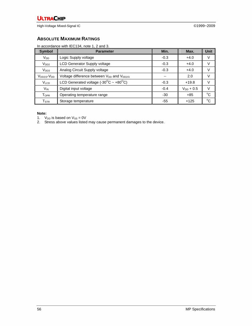
UUUULTRALTRALTRALTRACCCCHIPHIPHIPHIP
High-Voltage Mixed-Signal IC ©1999~2009
56 MP Specifications
ABSOLUTE MAXIMUM RATINGS In accordance with IEC134, note 1, 2 and 3.
Symbol Parameter Min. Max. Unit
VDD Logic Supply voltage -0.3 +4.0 V
VDD2 LCD Generator Supply voltage -0.3 +4.0 V
VDD3 Analog Circuit Supply voltage -0.3 +4.0 V
VDD2/3-VDD Voltage difference between VDD and VDD2/3 -- 2.0 V
VLCD LCD Generated voltage (-30OC ~ +80OC) -0.3 +19.8 V
VIN Digital input voltage -0.4 VDD + 0.5 V
TOPR Operating temperature range -30 +85 oC
TSTR Storage temperature -55 +125 oC
Note: 1. VDD is based on VSS = 0V 2. Stress above values listed may cause permanent damages to the device.

UC1611S 160x256/16S Matrix LCD Controller-Driver
Revision A1.43 57
SPECIFICATIONS DC CHARACTERISTICS
Symbol Parameter Conditions Min. Typ. Max. Unit
VDD Supply for digital circuit 1.65 1.8~3.3 3.6 V
VDD2/3 Supply for bias & pump 2.7 2.8~3.3 3.6 V
VLCD Charge pump output VDD2/3 2.4V, 25OC 17 17.5 V
VD LCD data voltage VDD2/3 2.4V, 25OC 1.69 V
VIL Input logic LOW 0.2VDD V
VIH Input logic HIGH 0.8VDD V
VOL Output logic LOW 0.2VDD V
VOH Output logic HIGH 0.8VDD V
IIL Input leakage current 1.5 µA
CIN Input capacitance 5 10 pF
COUT Output capacitance 5 10 pF
R0(SEG) SEG output impedance VLCD = 17V 1.35 2.5 k Ω
R0(COM) COM output impedance VLCD = 17V 1.35 2.5 k Ω
fLINE Average Line rate LC[5:4] = 10b -10% 28 +10% kHz
POWER CONSUMPTION VDD = 2.7 V, Bias Ratio = 11, PM = 234, VLCD = 17.01 V, Line Rate = 10 b, Panel Loading (PC[1:0]) = 11 b, Mux Rate = 160, Bus mode = 6800, CL = 500 nF, CB = 5 µF, Temperature = 25 oC, MTP= 00 H, All HV outputs are open circuit.
Display Pattern Conditions Typ. (µA) Max. (µA)
All-OFF Bus = idle 1656 2484
2-pixel checker Bus = idle 2031 3046
-- Bus = idle (standby current) -- 5
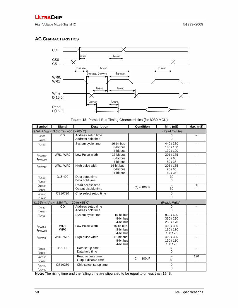
UUUULTRALTRALTRALTRACCCCHIPHIPHIPHIP
High-Voltage Mixed-Signal IC ©1999~2009
58 MP Specifications
AC CHARACTERISTICS
FIGURE 18: Parallel Bus Timing Characteristics (for 8080 MCU)
Symbol Signal Description Condition Min. (nS) Max. (nS)
(2.5V VDD< 3.6V, Ta= –30 to +85oC) (Read / Write)
tAS80
tAH80 CD Address setup time
Address hold time 0
0 –
tCY80 System cycle time 16-bit bus 8-bit bus 4-bit bus
440 / 360 180 / 160 130 / 100
–
tPWR80
tPWW80 WR1, WR0 Low Pulse width 16-bit bus
8-bit bus 4-bit bus
205 / 165 75 / 65 50 / 35
–
tHPW80 WR1, WR0 High pulse width 16-bit bus 8-bit bus 4-bit bus
205 / 165 75 / 65 50 / 35
–
tDS80
tDH80 D15~D0 Data setup time
Data hold time 30
0 –
tACC80
tOD80 Read access time
Output disable time CL = 100pF –
30 60 –
tSSA80 tCSH80
CS1/CS0 Chip select setup time 0 0
(1.65V VDD< 2.5V, Ta= –30 to +85oC) (Read / Write)
tAS80
tAH80 CD Address setup time
Address hold time 0
0 –
tCY80 System cycle time 16-bit bus 8-bit bus 4-bit bus
830 / 630 330 / 290 230 / 170
–
tPWR80 tPWW80
WR1 WR0
Low Pulse width 16-bit bus 8-bit bus 4-bit bus
400 / 300 150 / 130 100 / 70
–
tHPW80 WR1, WR0 High pulse width 16-bit bus 8-bit bus 4-bit bus
400 / 300 150 / 130 100 / 70
–
tDS80
tDH80 D15~D0 Data setup time
Data hold time 60
0 –
tACC80
tOD80 Read access time
Output disable time CL = 100pF –
50 120 –
tSSA80 tCSH80
CS1/CS0 Chip select setup time 0 0
Note: The rising time and the falling time are stipulated to be equal to or less than 15nS.
CD
tAS80 tAH80 CS0 CS1 tCSSA80 tCY80 tCSH80
tPWR80, tPWW80 tHPW80 WR0, WR1
tDS80 tDH80
Write D[15:0] tACC80 tOD80
Read D[15:0]
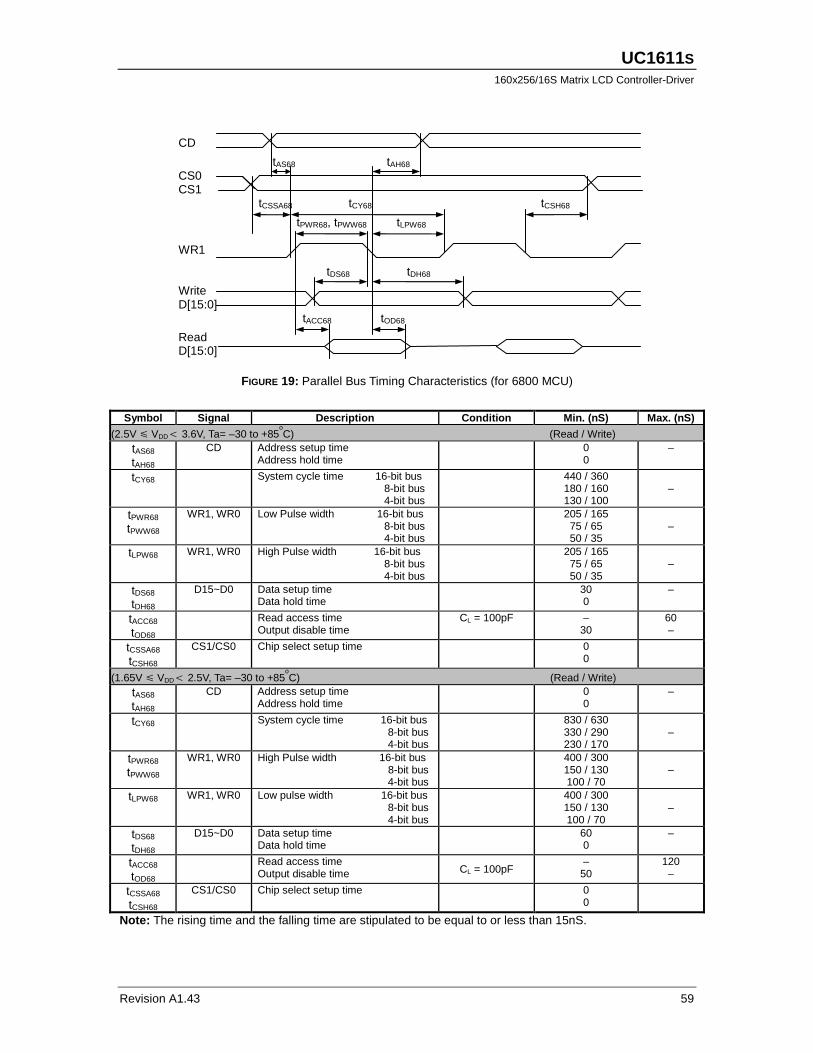
UC1611S 160x256/16S Matrix LCD Controller-Driver
Revision A1.43 59
FIGURE 19: Parallel Bus Timing Characteristics (for 6800 MCU)
Symbol Signal Description Condition Min. (nS) Max. (nS)
(2.5V VDD< 3.6V, Ta= –30 to +85oC) (Read / Write)
tAS68
tAH68 CD Address setup time
Address hold time 0
0 –
tCY68 System cycle time 16-bit bus 8-bit bus 4-bit bus
440 / 360 180 / 160 130 / 100
–
tPWR68 tPWW68
WR1, WR0 Low Pulse width 16-bit bus 8-bit bus 4-bit bus
205 / 165 75 / 65 50 / 35
–
tLPW68 WR1, WR0 High Pulse width 16-bit bus 8-bit bus 4-bit bus
205 / 165 75 / 65 50 / 35
–
tDS68
tDH68 D15~D0 Data setup time
Data hold time 30
0 –
tACC68
tOD68 Read access time
Output disable time CL = 100pF –
30 60 –
tCSSA68 tCSH68
CS1/CS0 Chip select setup time 0 0
(1.65V VDD< 2.5V, Ta= –30 to +85oC) (Read / Write)
tAS68
tAH68 CD Address setup time
Address hold time 0
0 –
tCY68 System cycle time 16-bit bus 8-bit bus 4-bit bus
830 / 630 330 / 290 230 / 170
–
tPWR68 tPWW68
WR1, WR0 High Pulse width 16-bit bus 8-bit bus 4-bit bus
400 / 300 150 / 130 100 / 70
–
tLPW68 WR1, WR0 Low pulse width 16-bit bus 8-bit bus 4-bit bus
400 / 300 150 / 130 100 / 70
–
tDS68
tDH68 D15~D0 Data setup time
Data hold time 60
0 –
tACC68
tOD68 Read access time
Output disable time CL = 100pF –
50 120 –
tCSSA68 tCSH68
CS1/CS0 Chip select setup time 0 0
Note: The rising time and the falling time are stipulated to be equal to or less than 15nS.
CD
tAS68 tAH68 CS0 CS1 tCSSA68 tCY68 tCSH68
tPWR68, tPWW68 tLPW68 WR1
tDS68 tDH68
Write D[15:0] tACC68 tOD68
Read D[15:0]

UUUULTRALTRALTRALTRACCCCHIPHIPHIPHIP
High-Voltage Mixed-Signal IC ©1999~2009
60 MP Specifications
FIGURE 20: Serial Bus Timing Characteristics (for S8)
Symbol Signal Description Condition Min. (nS) Max. (nS)
(2.5V VDD< 3.6V, Ta= –30 to +85oC) (Read / Write)
tASS8 tAHS8
CD Address setup time Address hold time
0 0
– –
tCYS8 tLPWS8 tHPWS8
SCK System cycle time Low pulse width High pulse width
150 / 51 60 / 18 60 / 18
– – –
tACCS8
t ODS8 Read access time
Output disable time –
15 50 –
tDSS8
tDHS8 SDA Data setup time
Data hold time 15
0 – –
tCSSAS8 tCSHS8
CS1/CS0 Chip select setup time 0 / 0
0 / 0
(1.65V VDD< 2.5V, Ta= –30 to +85oC) (Read / Write)
tASS8 tAHS8
CD Address setup time Address hold time
0 0
– –
tCYS8 tLPWS8 tHPWS8
SCK System cycle time Low pulse width High pulse width
270 / 110 120 / 30 120 / 30
– – –
tACCS8
t ODS8 Read access time
Output disable time –
30 90 –
tDSS8
tDHS8 SDA Data setup time
Data hold time 30
5 –
tCSSAS8 tCSHS8
CS1/CS0 Chip select setup time 0 / 0
0 / 0
Note: The rising time and the falling time are stipulated to be equal to or less than 15nS.
CD
CS0
SCK
SDA Write
SDA Read
CS1
tASS8 tAHS8
tCSSAS8 tCYS8
tLPWS8 tHPWS8
tCSHS8
tDSS8 tDHS8
tACCS8 tODS8

UC1611S 160x256/16S Matrix LCD Controller-Driver
Revision A1.43 61
FIGURE 21: Serial Bus Timing Characteristics (for S9)
Symbol Signal Description Condition Min. (nS) Max. (nS)
(2.5V VDD< 3.6V, Ta= –30 to +85oC) (Read / Write)
tCYS9 tLPWS9 tHPWS9
SCK System cycle time Low pulse width High pulse width
150 / 51 60 / 18 60 / 18
– – –
t ACCS9
t ODS9 SDA Read access time
Output disable time –
15 50 –
tDSS9
tDHS9 SDA Data setup time
Data hold time 15
0 –
tCSSAS9 tCSHS9
CS1/CS0 Chip select setup time 0 / 0
0 / 0
(1.65V VDD< 2.5V, Ta= –30 to +85oC) (Read / Write)
tCYS9 tLPWS9 tHPWS9
SCK System cycle time Low pulse width High pulse width
270 / 90 120 / 30 120 / 30
– – –
tACCS9
t ODS9 SDA Read access time
Output disable time –
30 90 –
tDSS9
tDHS9 SDA Data setup time
Data hold time 30
5 –
tCSSAS9 tCSHS9
CS1/CS0 Chip select setup time 0 / 0
0 / 0
Note: The rising time and the falling time are stipulated to be equal to or less than 15 nS.
CS0
SCK
SDA Write
CS1
tCSSAS9 tCYS9
tLPWS9 tHPWS9
tCSHS9
tDSS9 tDHS9
tACCS9 tODS9 SDA Read
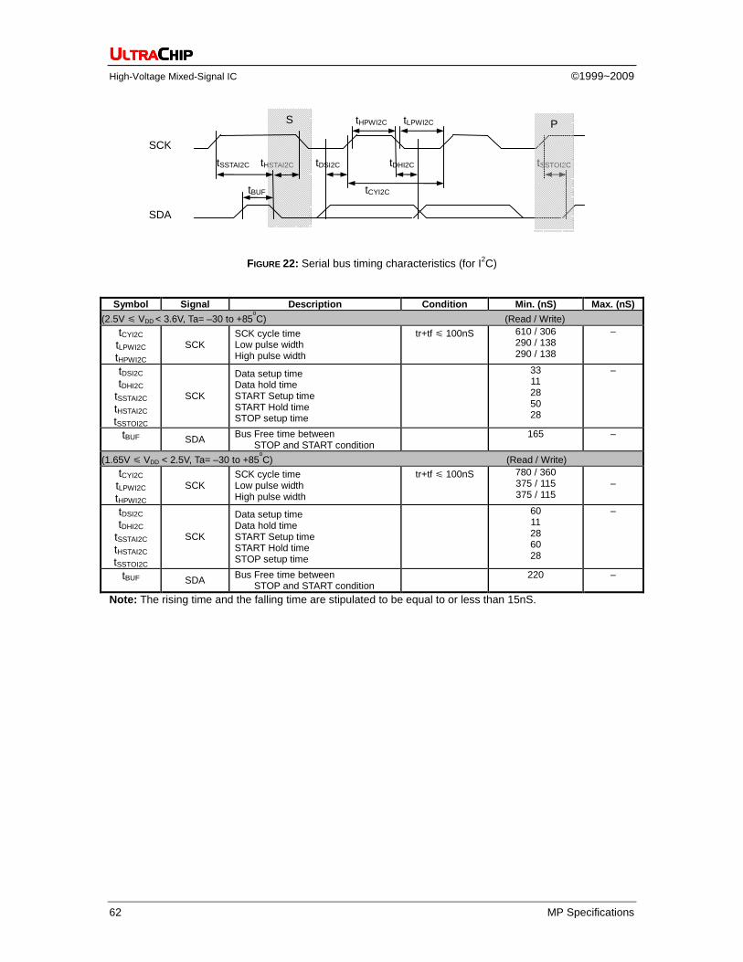
UUUULTRALTRALTRALTRACCCCHIPHIPHIPHIP
High-Voltage Mixed-Signal IC ©1999~2009
62 MP Specifications
FIGURE 22: Serial bus timing characteristics (for I2C)
Symbol Signal Description Condition Min. (nS) Max. (nS)
(2.5V VDD < 3.6V, Ta= –30 to +85oC) (Read / Write)
tCYI2C tLPWI2C tHPWI2C
SCK SCK cycle time Low pulse width High pulse width
tr+tf 100nS
610 / 306 290 / 138 290 / 138
–
tDSI2C tDHI2C
tSSTAI2C tHSTAI2C tSSTOI2C
SCK
Data setup time Data hold time START Setup time START Hold time STOP setup time
33 11 28 50 28
–
tBUF SDA Bus Free time between STOP and START condition
165 –
(1.65V VDD < 2.5V, Ta= –30 to +85oC) (Read / Write)
tCYI2C tLPWI2C tHPWI2C
SCK SCK cycle time Low pulse width High pulse width
tr+tf 100nS
780 / 360 375 / 115 375 / 115
–
tDSI2C tDHI2C
tSSTAI2C tHSTAI2C tSSTOI2C
SCK
Data setup time Data hold time START Setup time START Hold time STOP setup time
60 11 28 60 28
–
tBUF SDA Bus Free time between STOP and START condition 220 –
Note: The rising time and the falling time are stipulated to be equal to or less than 15nS.
tHPWI2C tLPWI2C SCK
tSSTAI2C tHSTAI2C tDSI2C tDHI2C tSSTOI2C
tBUF tCYI2C SDA
S P

UC1611S 160x256/16S Matrix LCD Controller-Driver
Revision A1.43 63
RST
tRW
WR[1:0]
tRD
FIGURE 23: Reset Characteristics
Symbol Signal Description Condition Min. Max.
(1.65V VDD< 3.6V, Ta= –30 to +85oC)
tRW RST Reset low pulse width 3 µS –
tRD RST, WR Reset to WR pulse delay 10 mS –
Note: For each mode, the signal’s rising time and falling time (tf, tr) are stipulated to be equal to or less than 15nS.
tr 15nS tf 15nS
20%
80%

UUUULTRALTRALTRALTRACCCCHIPHIPHIPHIP
High-Voltage Mixed-Signal IC ©1999~2009
64 MP Specifications
PHYSICAL DIMENSIONS
DIE INFORMATION
DIE SIZE:
13754 µM x 1120 µM ±40 µM
DIE THICKNESS:
400 µM ± 20 µM
BUMP HEIGHT:
15 µM ±3 µM (HMAX - HMIN) within die 2µM
BUMP PITCH:
38 µM (Typ.)
BUMP SIZE:
SEG/COM: 25 x 75.5 µM2 (Typ.)
BUMP AREA:
1887.5 µM2
PAD COORDINATES:
Pad center
PAD ORIGIN:
Chip center
(Drawings and coordinates are in the circuit/bump view)

UC1611S 160x256/16S Matrix LCD Controller-Driver
Revision A1.43 65
ALIGNMENT MARK INFORMATION SHAPE OF THE ALIGNMENT MARK: COORDINATES:
X Y X Y Mark / Point Upper-Left Mark ( L ) Upper-Right Mark
1 -5160.4 394 -- -- 2 -5144.4 370 -- -- (L)
3 -5120.4 354 -- -- Down-Left Mark ( + ) Down-Right Mark ( + )
1 -5365.225 -453.5 5549 -453.5 2 -5345.225 -513.5 5569 -513.5 3 -5385.225 -473.5 5529 -473.5 4 -5325.225 -493.5 5589 -493.5
(+)
C -5355.225 -483.5 5559 -483.5
TOP METAL AND PASSIVATION:
1
2
3 4
C
NOTE:
Alignment marks are on Metal3 under Passivation.
The “+” mark is symmetric both horizontally and vertically.
(0,0)
D-Left Mark
D-Right Mark
1
2
3
Metal3 / 9KÅ
SiON / 10.5KÅ

UUUULTRALTRALTRALTRACCCCHIPHIPHIPHIP
High-Voltage Mixed-Signal IC ©1999~2009
66 MP Specifications
PAD COORDINATES
# Pad X Y W H 1 DUMMY -6785.5 -487.75 30 75.5
2 COM101 -6745 -487.75 25 75.5
3 COM103 -6707 -487.75 25 75.5
4 COM105 -6669 -487.75 25 75.5
5 COM107 -6631 -487.75 25 75.5
6 COM109 -6593 -487.75 25 75.5
7 COM111 -6555 -487.75 25 75.5
8 COM113 -6517 -487.75 25 75.5
9 COM115 -6479 -487.75 25 75.5
10 COM117 -6441 -487.75 25 75.5
11 COM119 -6403 -487.75 25 75.5
12 COM121 -6365 -487.75 25 75.5
13 COM123 -6327 -487.75 25 75.5
14 COM125 -6289 -487.75 25 75.5
15 COM127 -6251 -487.75 25 75.5
16 COM129 -6213 -487.75 25 75.5
17 COM131 -6175 -487.75 25 75.5
18 COM133 -6137 -487.75 25 75.5
19 COM135 -6099 -487.75 25 75.5
20 COM137 -6061 -487.75 25 75.5
21 COM139 -6023 -487.75 25 75.5
22 COM141 -5985 -487.75 25 75.5
23 COM143 -5947 -487.75 25 75.5
24 COM145 -5909 -487.75 25 75.5
25 COM147 -5871 -487.75 25 75.5
26 COM149 -5833 -487.75 25 75.5
27 COM151 -5795 -487.75 25 75.5
28 COM153 -5757 -487.75 25 75.5
29 COM155 -5719 -487.75 25 75.5
30 COM157 -5681 -487.75 25 75.5
31 COM159 -5643 -487.75 25 75.5
32 D15 -5227.975 -483.275 69.1 82.45
33 vdd -5156.425 -483.275 25 82.45
34 D14 -5084.875 -483.275 69.1 82.45
35 D13 -4999.775 -483.275 69.1 82.45
36 D12 -4914.675 -483.275 69.1 82.45
37 D11 -4829.575 -483.275 69.1 82.45
38 D10 -4744.475 -483.275 69.1 82.45
39 D9 -4659.375 -483.275 69.1 82.45
40 D8 -4574.275 -483.275 69.1 82.45
41 D7 -4489.175 -483.275 69.1 82.45
42 D6 -4404.075 -483.275 69.1 82.45
43 D5 -4318.975 -483.275 69.1 82.45
44 D4 -4233.875 -483.275 69.1 82.45
45 D3 -4148.775 -483.275 69.1 82.45
46 D2 -4063.675 -483.275 69.1 82.45
47 D1 -3978.575 -483.275 69.1 82.45
48 D0 -3893.475 -483.275 69.1 82.45
49 RST -3786.925 -481 65 87
50 CS0 -3705.325 -481 65 87
51 vdd -3625.525 -481 45 87
# Pad X Y W H 52 CS1 -3545.725 -481 65 87
53 CD -3464.125 -481 65 87
54 WR0 -3382.525 -481 65 87
55 vdd -3302.725 -481 45 87
56 WR1 -3222.925 -481 65 87
57 BM1 -3141.325 -481 65 87
58 vdd -3061.525 -481 45 87
59 BM0 -2981.725 -481 65 87
60 TST4 -2901.925 -481 45 87
61 TST4 -2841.925 -481 45 87
62 ID0 -2554.125 -481 65 87
63 vdd -2474.325 -481 45 87
64 ID1 -2394.525 -481 65 87
65 vss -2314.725 -481 45 87
66 vss -2254.725 -481 45 87
67 vss -2194.725 -481 45 87
68 vss -2134.725 -481 45 87
69 vss -2074.725 -481 45 87
70 vss -2014.725 -481 45 87
71 vss -1954.725 -481 45 87
72 vss -1894.725 -481 45 87
73 vss -1834.725 -481 45 87
74 vss -1774.725 -481 45 87
75 vss -1714.725 -481 45 87
76 vss2 -1541.725 -481 45 87
77 vss2 -1481.725 -481 45 87
78 vss2 -1421.725 -481 45 87
79 vss2 -1361.725 -481 45 87
80 vss2 -1301.725 -481 45 87
81 vss2 -1241.725 -481 45 87
82 vss2 -1181.725 -481 45 87
83 vss2 -1121.725 -481 45 87
84 vss2 -1061.725 -481 45 87
85 vss2 -1001.725 -481 45 87
86 vss2 -941.725 -481 45 87
87 vdd2 -881.725 -481 45 87
88 vdd2 -821.725 -481 45 87
89 vdd2 -761.725 -481 45 87
90 vdd2 -701.725 -481 45 87
91 vdd2 -641.725 -481 45 87
92 vdd2 -581.725 -481 45 87
93 vdd2 -521.725 -481 45 87
94 vdd2 -461.725 -481 45 87
95 vdd2 -401.725 -481 45 87
96 vdd2 -341.725 -481 45 87
97 DUMMY -163.375 -481 45 87
98 vdd3 14.975 -481 45 87
99 vdd3 74.975 -481 45 87
100 vdd3 134.975 -481 45 87
101 vdd3 194.975 -481 45 87
102 vdd 254.975 -481 45 87

UC1611S 160x256/16S Matrix LCD Controller-Driver
Revision A1.43 67
# Pad X Y W H 103 vdd 314.975 -481 45 87
104 vdd 374.975 -481 45 87
105 vdd 434.975 -481 45 87
106 vdd 494.975 -481 45 87
107 vdd 554.975 -481 45 87
108 vdd 614.975 -481 45 87
109 vdd 674.975 -481 45 87
110 vdd 734.975 -481 45 87
111 vdd 794.975 -481 45 87
112 vdd 854.975 -481 45 87
113 DUMMY 1040.425 -481 45 87
114 DUMMY 1100.425 -481 45 87
115 DUMMY 1160.425 -481 45 87
116 DUMMY 1220.425 -481 45 87
117 DUMMY 1280.425 -481 45 87
118 DUMMY 1340.425 -481 45 87
119 DUMMY 1400.425 -481 45 87
120 DUMMY 1460.425 -481 45 87
121 TST2 1650.475 -481 45 87
122 TST1 1710.475 -481 45 87
123 VLCDIN 2050.35 -481 45 87
124 VLCDIN 2110.35 -481 45 87
125 VLCDOUT 2170.35 -481 45 87
126 VLCDOUT 2230.35 -481 45 87
127 VA0- 2642.35 -481 45 87
128 VA0- 2702.35 -481 45 87
129 VA0- 2762.35 -481 45 87
130 VA0- 2822.35 -481 45 87
131 VA1- 2882.35 -481 45 87
132 VA1- 2942.35 -481 45 87
133 VA1- 3002.35 -481 45 87
134 VA1- 3062.35 -481 45 87
135 VA1+ 3402.35 -481 45 87
136 VA1+ 3462.35 -481 45 87
137 VA1+ 3522.35 -481 45 87
138 VA1+ 3582.35 -481 45 87
139 VA0+ 3642.35 -481 45 87
140 VA0+ 3702.35 -481 45 87
141 VA0+ 3762.35 -481 45 87
142 VA0+ 3822.35 -481 45 87
143 VB0- 4162.35 -481 45 87
144 VB0- 4222.35 -481 45 87
145 VB0- 4282.35 -481 45 87
146 VB0- 4342.35 -481 45 87
147 VB1- 4402.35 -481 45 87
148 VB1- 4462.35 -481 45 87
149 VB1- 4522.35 -481 45 87
150 VB1- 4582.35 -481 45 87
151 VB1+ 4922.35 -481 45 87
152 VB1+ 4982.35 -481 45 87
153 VB1+ 5042.35 -481 45 87
154 VB1+ 5102.35 -481 45 87
155 VB0+ 5162.35 -481 45 87
# Pad X Y W H 156 VB0+ 5222.35 -481 45 87
157 VB0+ 5282.35 -481 45 87
158 VB0+ 5342.35 -481 45 87
159 COM160 5643 -487.75 25 75.5
160 COM158 5681 -487.75 25 75.5
161 COM156 5719 -487.75 25 75.5
162 COM154 5757 -487.75 25 75.5
163 COM152 5795 -487.75 25 75.5
164 COM150 5833 -487.75 25 75.5
165 COM148 5871 -487.75 25 75.5
166 COM146 5909 -487.75 25 75.5
167 COM144 5947 -487.75 25 75.5
168 COM142 5985 -487.75 25 75.5
169 COM140 6023 -487.75 25 75.5
170 COM138 6061 -487.75 25 75.5
171 COM136 6099 -487.75 25 75.5
172 COM134 6137 -487.75 25 75.5
173 COM132 6175 -487.75 25 75.5
174 COM130 6213 -487.75 25 75.5
175 COM128 6251 -487.75 25 75.5
176 COM126 6289 -487.75 25 75.5
177 COM124 6327 -487.75 25 75.5
178 COM122 6365 -487.75 25 75.5
179 COM120 6403 -487.75 25 75.5
180 COM118 6441 -487.75 25 75.5
181 COM116 6479 -487.75 25 75.5
182 COM114 6517 -487.75 25 75.5
183 COM112 6555 -487.75 25 75.5
184 COM110 6593 -487.75 25 75.5
185 COM108 6631 -487.75 25 75.5
186 COM106 6669 -487.75 25 75.5
187 COM104 6707 -487.75 25 75.5
188 COM102 6745 -487.75 25 75.5
189 DUMMY 6785.5 -487.75 30 75.5
190 DUMMY 6785.5 487.75 30 75.5
191 COM100 6745 487.75 25 75.5
192 COM98 6707 487.75 25 75.5
193 COM96 6669 487.75 25 75.5
194 COM94 6631 487.75 25 75.5
195 COM92 6593 487.75 25 75.5
196 COM90 6555 487.75 25 75.5
197 COM88 6517 487.75 25 75.5
198 COM86 6479 487.75 25 75.5
199 COM84 6441 487.75 25 75.5
200 COM82 6403 487.75 25 75.5
201 COM80 6365 487.75 25 75.5
202 COM78 6327 487.75 25 75.5
203 COM76 6289 487.75 25 75.5
204 COM74 6251 487.75 25 75.5
205 COM72 6213 487.75 25 75.5
206 COM70 6175 487.75 25 75.5
207 COM68 6137 487.75 25 75.5
208 COM66 6099 487.75 25 75.5

UUUULTRALTRALTRALTRACCCCHIPHIPHIPHIP
High-Voltage Mixed-Signal IC ©1999~2009
68 MP Specifications
# Pad X Y W H 209 COM64 6061 487.75 25 75.5
210 COM62 6023 487.75 25 75.5
211 COM60 5985 487.75 25 75.5
212 COM58 5947 487.75 25 75.5
213 COM56 5909 487.75 25 75.5
214 COM54 5871 487.75 25 75.5
215 COM52 5833 487.75 25 75.5
216 COM50 5795 487.75 25 75.5
217 COM48 5757 487.75 25 75.5
218 COM46 5719 487.75 25 75.5
219 COM44 5681 487.75 25 75.5
220 COM42 5643 487.75 25 75.5
221 COM40 5605 487.75 25 75.5
222 COM38 5567 487.75 25 75.5
223 COM36 5529 487.75 25 75.5
224 COM34 5491 487.75 25 75.5
225 COM32 5453 487.75 25 75.5
226 COM30 5415 487.75 25 75.5
227 COM28 5377 487.75 25 75.5
228 COM26 5339 487.75 25 75.5
229 COM24 5301 487.75 25 75.5
230 COM22 5263 487.75 25 75.5
231 COM20 5225 487.75 25 75.5
232 COM18 5187 487.75 25 75.5
233 COM16 5149 487.75 25 75.5
234 COM14 5111 487.75 25 75.5
235 COM12 5073 487.75 25 75.5
236 COM10 5035 487.75 25 75.5
237 COM8 4997 487.75 25 75.5
238 COM6 4959 487.75 25 75.5
239 COM4 4921 487.75 25 75.5
240 COM2 4883 487.75 25 75.5
241 SEG1 4845 487.75 25 75.5
242 SEG2 4807 487.75 25 75.5
243 SEG3 4769 487.75 25 75.5
244 SEG4 4731 487.75 25 75.5
245 SEG5 4693 487.75 25 75.5
246 SEG6 4655 487.75 25 75.5
247 SEG7 4617 487.75 25 75.5
248 SEG8 4579 487.75 25 75.5
249 SEG9 4541 487.75 25 75.5
250 SEG10 4503 487.75 25 75.5
251 SEG11 4465 487.75 25 75.5
252 SEG12 4427 487.75 25 75.5
253 SEG13 4389 487.75 25 75.5
254 SEG14 4351 487.75 25 75.5
255 SEG15 4313 487.75 25 75.5
256 SEG16 4275 487.75 25 75.5
257 SEG17 4237 487.75 25 75.5
258 SEG18 4199 487.75 25 75.5
259 SEG19 4161 487.75 25 75.5
260 SEG20 4123 487.75 25 75.5
261 SEG21 4085 487.75 25 75.5
# Pad X Y W H 262 SEG22 4047 487.75 25 75.5
263 SEG23 4009 487.75 25 75.5
264 SEG24 3971 487.75 25 75.5
265 SEG25 3933 487.75 25 75.5
266 SEG26 3895 487.75 25 75.5
267 SEG27 3857 487.75 25 75.5
268 SEG28 3819 487.75 25 75.5
269 SEG29 3781 487.75 25 75.5
270 SEG30 3743 487.75 25 75.5
271 SEG31 3705 487.75 25 75.5
272 SEG32 3667 487.75 25 75.5
273 SEG33 3629 487.75 25 75.5
274 SEG34 3591 487.75 25 75.5
275 SEG35 3553 487.75 25 75.5
276 SEG36 3515 487.75 25 75.5
277 SEG37 3477 487.75 25 75.5
278 SEG38 3439 487.75 25 75.5
279 SEG39 3401 487.75 25 75.5
280 SEG40 3363 487.75 25 75.5
281 SEG41 3325 487.75 25 75.5
282 SEG42 3287 487.75 25 75.5
283 SEG43 3249 487.75 25 75.5
284 SEG44 3211 487.75 25 75.5
285 SEG45 3173 487.75 25 75.5
286 SEG46 3135 487.75 25 75.5
287 SEG47 3097 487.75 25 75.5
288 SEG48 3059 487.75 25 75.5
289 SEG49 3021 487.75 25 75.5
290 SEG50 2983 487.75 25 75.5
291 SEG51 2945 487.75 25 75.5
292 SEG52 2907 487.75 25 75.5
293 SEG53 2869 487.75 25 75.5
294 SEG54 2831 487.75 25 75.5
295 SEG55 2793 487.75 25 75.5
296 SEG56 2755 487.75 25 75.5
297 SEG57 2717 487.75 25 75.5
298 SEG58 2679 487.75 25 75.5
299 SEG59 2641 487.75 25 75.5
300 SEG60 2603 487.75 25 75.5
301 SEG61 2565 487.75 25 75.5
302 SEG62 2527 487.75 25 75.5
303 SEG63 2489 487.75 25 75.5
304 SEG64 2451 487.75 25 75.5
305 SEG65 2413 487.75 25 75.5
306 SEG66 2375 487.75 25 75.5
307 SEG67 2337 487.75 25 75.5
308 SEG68 2299 487.75 25 75.5
309 SEG69 2261 487.75 25 75.5
310 SEG70 2223 487.75 25 75.5
311 SEG71 2185 487.75 25 75.5
312 SEG72 2147 487.75 25 75.5
313 SEG73 2109 487.75 25 75.5
314 SEG74 2071 487.75 25 75.5

UC1611S 160x256/16S Matrix LCD Controller-Driver
Revision A1.43 69
# Pad X Y W H 315 SEG75 2033 487.75 25 75.5
316 SEG76 1995 487.75 25 75.5
317 SEG77 1957 487.75 25 75.5
318 SEG78 1919 487.75 25 75.5
319 SEG79 1881 487.75 25 75.5
320 SEG80 1843 487.75 25 75.5
321 SEG81 1805 487.75 25 75.5
322 SEG82 1767 487.75 25 75.5
323 SEG83 1729 487.75 25 75.5
324 SEG84 1691 487.75 25 75.5
325 SEG85 1653 487.75 25 75.5
326 SEG86 1615 487.75 25 75.5
327 SEG87 1577 487.75 25 75.5
328 SEG88 1539 487.75 25 75.5
329 SEG89 1501 487.75 25 75.5
330 SEG90 1463 487.75 25 75.5
331 SEG91 1425 487.75 25 75.5
332 SEG92 1387 487.75 25 75.5
333 SEG93 1349 487.75 25 75.5
334 SEG94 1311 487.75 25 75.5
335 SEG95 1273 487.75 25 75.5
336 SEG96 1235 487.75 25 75.5
337 SEG97 1197 487.75 25 75.5
338 SEG98 1159 487.75 25 75.5
339 SEG99 1121 487.75 25 75.5
340 SEG100 1083 487.75 25 75.5
341 SEG101 1045 487.75 25 75.5
342 SEG102 1007 487.75 25 75.5
343 SEG103 969 487.75 25 75.5
344 SEG104 931 487.75 25 75.5
345 SEG105 893 487.75 25 75.5
346 SEG106 855 487.75 25 75.5
347 SEG107 817 487.75 25 75.5
348 SEG108 779 487.75 25 75.5
349 SEG109 741 487.75 25 75.5
350 SEG110 703 487.75 25 75.5
351 SEG111 665 487.75 25 75.5
352 SEG112 627 487.75 25 75.5
353 SEG113 589 487.75 25 75.5
354 SEG114 551 487.75 25 75.5
355 SEG115 513 487.75 25 75.5
356 SEG116 475 487.75 25 75.5
357 SEG117 437 487.75 25 75.5
358 SEG118 399 487.75 25 75.5
359 SEG119 361 487.75 25 75.5
360 SEG120 323 487.75 25 75.5
361 SEG121 285 487.75 25 75.5
362 SEG122 247 487.75 25 75.5
363 SEG123 209 487.75 25 75.5
364 SEG124 171 487.75 25 75.5
365 SEG125 133 487.75 25 75.5
366 SEG126 95 487.75 25 75.5
367 SEG127 57 487.75 25 75.5
# Pad X Y W H 368 SEG128 19 487.75 25 75.5
369 SEG129 -19 487.75 25 75.5
370 SEG130 -57 487.75 25 75.5
371 SEG131 -95 487.75 25 75.5
372 SEG132 -133 487.75 25 75.5
373 SEG133 -171 487.75 25 75.5
374 SEG134 -209 487.75 25 75.5
375 SEG135 -247 487.75 25 75.5
376 SEG136 -285 487.75 25 75.5
377 SEG137 -323 487.75 25 75.5
378 SEG138 -361 487.75 25 75.5
379 SEG139 -399 487.75 25 75.5
380 SEG140 -437 487.75 25 75.5
381 SEG141 -475 487.75 25 75.5
382 SEG142 -513 487.75 25 75.5
383 SEG143 -551 487.75 25 75.5
384 SEG144 -589 487.75 25 75.5
385 SEG145 -627 487.75 25 75.5
386 SEG146 -665 487.75 25 75.5
387 SEG147 -703 487.75 25 75.5
388 SEG148 -741 487.75 25 75.5
389 SEG149 -779 487.75 25 75.5
390 SEG150 -817 487.75 25 75.5
391 SEG151 -855 487.75 25 75.5
392 SEG152 -893 487.75 25 75.5
393 SEG153 -931 487.75 25 75.5
394 SEG154 -969 487.75 25 75.5
395 SEG155 -1007 487.75 25 75.5
396 SEG156 -1045 487.75 25 75.5
397 SEG157 -1083 487.75 25 75.5
398 SEG158 -1121 487.75 25 75.5
399 SEG159 -1159 487.75 25 75.5
400 SEG160 -1197 487.75 25 75.5
401 SEG161 -1235 487.75 25 75.5
402 SEG162 -1273 487.75 25 75.5
403 SEG163 -1311 487.75 25 75.5
404 SEG164 -1349 487.75 25 75.5
405 SEG165 -1387 487.75 25 75.5
406 SEG166 -1425 487.75 25 75.5
407 SEG167 -1463 487.75 25 75.5
408 SEG168 -1501 487.75 25 75.5
409 SEG169 -1539 487.75 25 75.5
410 SEG170 -1577 487.75 25 75.5
411 SEG171 -1615 487.75 25 75.5
412 SEG172 -1653 487.75 25 75.5
413 SEG173 -1691 487.75 25 75.5
414 SEG174 -1729 487.75 25 75.5
415 SEG175 -1767 487.75 25 75.5
416 SEG176 -1805 487.75 25 75.5
417 SEG177 -1843 487.75 25 75.5
418 SEG178 -1881 487.75 25 75.5
419 SEG179 -1919 487.75 25 75.5
420 SEG180 -1957 487.75 25 75.5
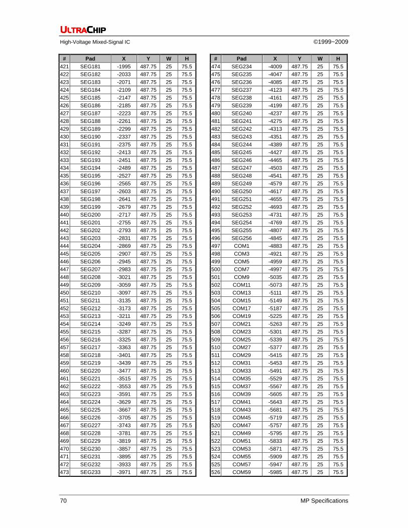
UUUULTRALTRALTRALTRACCCCHIPHIPHIPHIP
High-Voltage Mixed-Signal IC ©1999~2009
70 MP Specifications
# Pad X Y W H 421 SEG181 -1995 487.75 25 75.5
422 SEG182 -2033 487.75 25 75.5
423 SEG183 -2071 487.75 25 75.5
424 SEG184 -2109 487.75 25 75.5
425 SEG185 -2147 487.75 25 75.5
426 SEG186 -2185 487.75 25 75.5
427 SEG187 -2223 487.75 25 75.5
428 SEG188 -2261 487.75 25 75.5
429 SEG189 -2299 487.75 25 75.5
430 SEG190 -2337 487.75 25 75.5
431 SEG191 -2375 487.75 25 75.5
432 SEG192 -2413 487.75 25 75.5
433 SEG193 -2451 487.75 25 75.5
434 SEG194 -2489 487.75 25 75.5
435 SEG195 -2527 487.75 25 75.5
436 SEG196 -2565 487.75 25 75.5
437 SEG197 -2603 487.75 25 75.5
438 SEG198 -2641 487.75 25 75.5
439 SEG199 -2679 487.75 25 75.5
440 SEG200 -2717 487.75 25 75.5
441 SEG201 -2755 487.75 25 75.5
442 SEG202 -2793 487.75 25 75.5
443 SEG203 -2831 487.75 25 75.5
444 SEG204 -2869 487.75 25 75.5
445 SEG205 -2907 487.75 25 75.5
446 SEG206 -2945 487.75 25 75.5
447 SEG207 -2983 487.75 25 75.5
448 SEG208 -3021 487.75 25 75.5
449 SEG209 -3059 487.75 25 75.5
450 SEG210 -3097 487.75 25 75.5
451 SEG211 -3135 487.75 25 75.5
452 SEG212 -3173 487.75 25 75.5
453 SEG213 -3211 487.75 25 75.5
454 SEG214 -3249 487.75 25 75.5
455 SEG215 -3287 487.75 25 75.5
456 SEG216 -3325 487.75 25 75.5
457 SEG217 -3363 487.75 25 75.5
458 SEG218 -3401 487.75 25 75.5
459 SEG219 -3439 487.75 25 75.5
460 SEG220 -3477 487.75 25 75.5
461 SEG221 -3515 487.75 25 75.5
462 SEG222 -3553 487.75 25 75.5
463 SEG223 -3591 487.75 25 75.5
464 SEG224 -3629 487.75 25 75.5
465 SEG225 -3667 487.75 25 75.5
466 SEG226 -3705 487.75 25 75.5
467 SEG227 -3743 487.75 25 75.5
468 SEG228 -3781 487.75 25 75.5
469 SEG229 -3819 487.75 25 75.5
470 SEG230 -3857 487.75 25 75.5
471 SEG231 -3895 487.75 25 75.5
472 SEG232 -3933 487.75 25 75.5
473 SEG233 -3971 487.75 25 75.5
# Pad X Y W H 474 SEG234 -4009 487.75 25 75.5
475 SEG235 -4047 487.75 25 75.5
476 SEG236 -4085 487.75 25 75.5
477 SEG237 -4123 487.75 25 75.5
478 SEG238 -4161 487.75 25 75.5
479 SEG239 -4199 487.75 25 75.5
480 SEG240 -4237 487.75 25 75.5
481 SEG241 -4275 487.75 25 75.5
482 SEG242 -4313 487.75 25 75.5
483 SEG243 -4351 487.75 25 75.5
484 SEG244 -4389 487.75 25 75.5
485 SEG245 -4427 487.75 25 75.5
486 SEG246 -4465 487.75 25 75.5
487 SEG247 -4503 487.75 25 75.5
488 SEG248 -4541 487.75 25 75.5
489 SEG249 -4579 487.75 25 75.5
490 SEG250 -4617 487.75 25 75.5
491 SEG251 -4655 487.75 25 75.5
492 SEG252 -4693 487.75 25 75.5
493 SEG253 -4731 487.75 25 75.5
494 SEG254 -4769 487.75 25 75.5
495 SEG255 -4807 487.75 25 75.5
496 SEG256 -4845 487.75 25 75.5
497 COM1 -4883 487.75 25 75.5
498 COM3 -4921 487.75 25 75.5
499 COM5 -4959 487.75 25 75.5
500 COM7 -4997 487.75 25 75.5
501 COM9 -5035 487.75 25 75.5
502 COM11 -5073 487.75 25 75.5
503 COM13 -5111 487.75 25 75.5
504 COM15 -5149 487.75 25 75.5
505 COM17 -5187 487.75 25 75.5
506 COM19 -5225 487.75 25 75.5
507 COM21 -5263 487.75 25 75.5
508 COM23 -5301 487.75 25 75.5
509 COM25 -5339 487.75 25 75.5
510 COM27 -5377 487.75 25 75.5
511 COM29 -5415 487.75 25 75.5
512 COM31 -5453 487.75 25 75.5
513 COM33 -5491 487.75 25 75.5
514 COM35 -5529 487.75 25 75.5
515 COM37 -5567 487.75 25 75.5
516 COM39 -5605 487.75 25 75.5
517 COM41 -5643 487.75 25 75.5
518 COM43 -5681 487.75 25 75.5
519 COM45 -5719 487.75 25 75.5
520 COM47 -5757 487.75 25 75.5
521 COM49 -5795 487.75 25 75.5
522 COM51 -5833 487.75 25 75.5
523 COM53 -5871 487.75 25 75.5
524 COM55 -5909 487.75 25 75.5
525 COM57 -5947 487.75 25 75.5
526 COM59 -5985 487.75 25 75.5

UC1611S 160x256/16S Matrix LCD Controller-Driver
Revision A1.43 71
# Pad X Y W H 527 COM61 -6023 487.75 25 75.5
528 COM63 -6061 487.75 25 75.5
529 COM65 -6099 487.75 25 75.5
530 COM67 -6137 487.75 25 75.5
531 COM69 -6175 487.75 25 75.5
532 COM71 -6213 487.75 25 75.5
533 COM73 -6251 487.75 25 75.5
534 COM75 -6289 487.75 25 75.5
535 COM77 -6327 487.75 25 75.5
536 COM79 -6365 487.75 25 75.5
537 COM81 -6403 487.75 25 75.5
538 COM83 -6441 487.75 25 75.5
539 COM85 -6479 487.75 25 75.5
540 COM87 -6517 487.75 25 75.5
541 COM89 -6555 487.75 25 75.5
542 COM91 -6593 487.75 25 75.5
543 COM93 -6631 487.75 25 75.5
544 COM95 -6669 487.75 25 75.5
545 COM97 -6707 487.75 25 75.5
546 COM99 -6745 487.75 25 75.5
547 DUMMY -6785.5 487.75 30 75.5

UUUULTRALTRALTRALTRACCCCHIPHIPHIPHIP
High-Voltage Mixed-Signal IC ©1999~2009
72 MP Specifications
TRAY INFORMATION
SPEC
±0.10
±0.10
±0.10
±0.10
±0.06
±0.06
±0.10
±0.10
3x20=60
20-549x52-24
L2L3L1
P1
P2
T
L3
L1
L2
P1
P2
T
±0.06
±0.06
±0.06
Z
Z
Sx
Sy
S
1.17
1.17X
Px
10°
Py Y10°
N/A
Rev.
A4
A
Proj.
N/A
N/A
N/A
Draw
ing No.
Approved
Material
Package C
ode
Scale
1 of 1S
heet
Joan
Size
Draw
n 2 吋單
面萃
mm
drawing
detail
see
N/A
01-22-08'D
ateN
/AJack C
hungB
y
Unit
Angle
General
Tolerance
Dim
ension
Roughness
Unless O
therwise
Specified
Jack Chung
Checked
ULTRACHIP
INC.
晶 宏
半 導
體
01-22-08'01-22-08'

UC1611S 160x256/16S Matrix LCD Controller-Driver
Revision A1.43 73
H20-52x546-22
N/A
Rev.
A4
B
Proj.
N/A
N/A
N/A
Draw
ing No.
Approved
Material
Package C
ode
Scale
1 of 1S
heet
Jack chung
Size
Draw
n
2 " double-faced tray
mm
drawing
detail
see
N/A
03-16-09'D
ateN
/AC
indy B
y
Unit
Angle
General
Tolerance
Dim
ension
Roughness
Unless O
therwise
Specified
Cindy
Checked
ULTRACHIP
INC.
晶 宏 半 導
體
03-16-09'03-17-09'

UUUULTRALTRALTRALTRACCCCHIPHIPHIPHIP
High-Voltage Mixed-Signal IC ©1999~2009
74 MP Specifications
REVISION HISTORY
Revision Contents Date
0.6 First-time release Apr. 28, ‘08 (1) The relationship between VDD and VDD2/3 is adjusted to make VDD2/3 between VDD ~ VDD+1.5V (Section “Pin Description” – VDD VDD2 VDD3, p 6) (2) The description of connection of capacitors is updated. (Section “Pin Description” – CAX/CBX, p 6) (3) The recommended CB value is adjusted: 100~150 times 100~250 times of … (Section “Pin Description” – Notes, p 6; “Hi-V Generator and Bias Reference Circuit”, p 30) (4) The formula of Mux-rate is updated to DEN-DST+1+LC[3] x FL x 2 (Section “Control Registers” – LC, p 12; “Command Description” – (14), p 19; “Command Description” – (30), p 24) (5) The description of LC[3] is updated. (Section “Command Description” – (21), p 22) (6) The description of the command is updated. (Section “Command Description” – (9), p 18) (7) The VLCD chart and the table are updated. (Section “VLCD Quick Reference”, p 29) (8) Figures 4a and 5a illustrating Read in S8 and S9 modes are inserted. (Section “Host Interfaces”, Pp 36~37) (9) The description on Sleep Mode and Draining Circuit is updated. (Section “Reset and Power Management”, p 49) (10) The description of Power-Down Sequence is updated. (Section “Reset & Power Management”, p 50) (11) The settings of MTP2/3 for MTP Read/Program/Erase are updated: for Program/Erase, MTP3 : 28h 25h for Read, MTP2 : 6Fh 69h (Section “MTP Operation for LCM Makers”, p 51; “MTP Command Sequence Sample Codes”, Pp 54~55) (12) VDD2/3 - VDD (Max.) is adjusted: 1.2V 2.0V (Section ”Absolute Maximum Ratings”, p 58) (13) Input logic Low, VIL (Max.), is adjusted : 0.15 0.2 times of VDD
Input logic High, VIH (Min.), is adjusted : 0.5 0.8 times of VDD SEG output impedance, R0(SEG) (Typ.), is adjusted : 1.2 1.35 kΩ COM output impedance, R0(COM) (Typ.), is adjusted : 1.2 1.35 kΩ (Section “Specifications” – DC Characteristics, p 59) (14) Power consumption data (maximum) present. (Section “Specifications” – Power Consumption, p 59)
1.0
(15) AC timings are adjusted. (Section “AC Characteristics”, Pp 60~66)
Jun. 11, ‘08
(1) CA is added to the Note description. (Section “Pin Description”, p 6; “Hi-V Generator & Bias Reference Circuit”, p 30) 1.1 (2) The example under the RAM table is corrected. (Section “Display Data RAM”, p 48)
Aug. 7, ‘08
1.2 (1) The Y coordinates of pins 1 to 31 are corrected: -487.5 -487.75 (Section “Pad Coordinates”, p 70) Sep. 4, ‘08
1.3 (1) The COG drawing is updated. (Section “Recommended COG Layout”, p 10) Dec. 15, ‘08

UC1611S 160x256/16S Matrix LCD Controller-Driver
Revision A1.43 75
Revision Contents Date
(1) Number of bits of MTPC : 5 6 (Section “Control Register”, p 13)
1.31 (2) Some MTP names are corrected: MTP3 MTP2, MTP2 MTP1, MTP4 MTP3, MTP5 MTP4
(Section “MTP OPERATION FOR LCM MAKERS”, Pp 52~55)
Jan. 13, ‘09
1.4 (1) One more tray drawing is added. (Section “Tray Information”, p 75) Mar. 19, ‘09
(1) The number of bits is corrected to include D6. (Section "Command Table" - (32)(34), p 15; "Command Description", p 25)
(2) The command name is corrected: Column Row (Section "Command Table" - (34), p 15)
(3) The numbering of SEGs in the RAM table is corrected. (Section “Display Data RAM”, Pp 47~48)
(4) The command code for PMO is corrected. D6 : 1 0 (Section "MTP Operation for LCM Makers" – Table “MTP Erase Sample Code”, p 55)
(5) A note on rising edge and falling edge is added. (Section “AC Characteristics”, p 65)
1.41
(6) The Passivation drawing is updated. (Section “Alignment Mark Information”, p 67)
Jun. 10, ‘09
1.42 (1) A legacy error is corrected: row address page address. (overall) Jun. 23, ‘09
1.43 (1) Cycle times are adjusted by adding rising time and falling time. (Section “AC Characteristics”, Pp 58~63) Jul. 3, ‘09
![SLC NAND FLASH and LPDDR2 162-Ball MCP (Multi-Chip Package) · /cs vrefca vss vrefdq zq rzq dq[31:0]/dq[15:0] dqs cke ck /ck dm ca[9:0] vdd1 vdd2 vddq vddca vssq vssca](https://static.fdocuments.us/doc/165x107/5e6ef84ba26dbc791f49bd5b/slc-nand-flash-and-lpddr2-162-ball-mcp-multi-chip-package-cs-vrefca-vss-vrefdq.jpg)