Development of Sign Signal Translation System Based on Altera’s FPGA DE2 Board

Using the SDRAM Memory on Altera’s DE2 Boardwith VHDL Design
This tutorial explains how the SDRAM chip on Altera’s DE2 Development and Education board can be usedwith a Nios II system implemented by using the Altera SOPC Builder. The discussion is based on the assumptionthat the reader has access to a DE2 board and is familiar with the material in the tutorialIntroduction to the AlteraSOPC Builder Using VHDL Design.
The screen captures in the tutorial were obtained using the QuartusR© II version 8.0; if other versions of thesoftware are used, some of the images may be slightly different.
Contents:Example Nios II SystemThe SDRAM InterfaceUsing the SOPC Builder to Generate the Nios II SystemIntegration of the Nios II System into the Quartus II ProjectUsing a Phase-Locked Loop
1

The introductory tutorialIntroduction to the Altera SOPC Builder Using VHDL Designexplains how thememory in the Cyclone II FPGA chip can be used in the context ofa simple Nios II system. For practicalapplications it is necessary to have a much larger memory. The Altera DE2 board contains an SDRAM chipthat can store 8 Mbytes of data. This memory is organized as 1Mx 16 bits x 4 banks. The SDRAM chiprequires careful timing control. To provide access to the SDRAM chip, the SOPC Builder implements anSDRAMController circuit. This circuit generates the signals needed to deal with the SDRAM chip.
1 Example Nios II System
As an illustrative example, we will add the SDRAM to the Nios II system described in theIntroduction to theAltera SOPC Builder Using VHDL Designtutorial. Figure 1 gives the block diagram of our example system.
On-chipmemory
parallel input
interface
parallel output
interface
Avalon switch fabric
Nios II processorJTAG UART
interface
USB-Blaster
interface
Host computer
Cyclone II
FPGA chip
SW7 SW0 LEDG7 LEDG0
Reset_n Clock
LEDs
JTAG Debug
module
SwitchesSDRAMcontroller
SDRAMchip
Figure 1. Example Nios II system implemented on the DE2 board.
The system realizes a trivial task. Eight toggle switches onthe DE2 board,SW7−0, are used to turn on or offthe eight green LEDs,LEDG7 − 0. The switches are connected to the Nios II system by means of aparallel I/O
2

interface configured to act as an input port. The LEDs are driven by the signals from another parallel I/O interfaceconfigured to act as an output port. To achieve the desired operation, the eight-bit pattern corresponding to thestate of the switches has to be sent to the output port to activate the LEDs. This will be done by having the Nios IIprocessor execute an application program. Continuous operation is required, such that as the switches are toggledthe lights change accordingly.
The introductory tutorial showed how we can use the SOPC Builder to design the hardware needed to imple-ment this task, assuming that the application program whichreads the state of the toggle switches and sets thegreen LEDs accordingly is loaded into a memory block in the FPGA chip. In this tutorial, we will explain how theSDRAM chip on the DE2 board can be included in the system in Figure 1, so that our application program can berun from the SDRAM rather than from the on-chip memory.
Doing this tutorial, the reader will learn about:
• Using the SOPC Builder to include an SDRAM interface for a Nios II-based system
• Timing issues with respect to the SDRAM on the DE2 board
• Using a phase-locked loop (PLL) to control the clock timing
2 The SDRAM Interface
The SDRAM chip on the DE2 board has the capacity of 64 Mbits (8 Mbytes). It is organized as 1Mx 16 bitsx4 banks. The signals needed to communicate with this chip areshown in Figure 2. All of the signals, except theclock, can be provided by the SDRAM Controller that can be generated by using the SOPC Builder. The clocksignal is provided separately. It has to meet the clock-skewrequirements as explained in section 5. Note that somesignals are active low, which is denoted by the suffix N.
Clock
Bank Address 1
Address
Clock Enable
Column Address Strobe
High-byte Data Mask
CLK
CKE
ADDR[11:0]
BA1Bank Address 0
Chip Select
Row Address Strobe
Write Enable
Data
Low-byte Data Mask
BA0
CS_N
CAS_N
RAS_N
WE_N
DQ[15:0]
UDQM
LDQM
SDRAM
chip
SDRAM
controller
Figure 2. The SDRAM signals.
3

3 Using the SOPC Builder to Generate the Nios II System
Our starting point will be the Nios II system discussed in theIntroduction to the Altera SOPC Builder Using VHDLDesigntutorial, which we implemented in a project calledlights. We specified the system shown in Figure 3.
Figure 3. The Nios II system defined in the introductory tutorial.
If you saved thelights project, then open this project in the Quartus II software and then open the SOPCBuilder. Otherwise, you need to create and implement the project, as explained in the introductory tutorial, toobtain the system shown in the figure.
To add the SDRAM, in the window of Figure 3 selectMemories and Memory Controllers > SDRAM >
SDRAM Controller and clickAdd. A window depicted in Figure 4 appears. SelectCustomfrom thePresetsdrop-down list. Set the Data Width parameter to 16 bits and leave the default values for the rest. Since we willnot simulate the system in this tutorial, do not select the option Include a functional memory model in thesystem testbench. Click Finish. Now, in the window of Figure 3, there will be ansdram module added tothe design. Select the commandSystem > Auto-Assign Base Addresses to produce the assignment shown inFigure 5. Observe that the SOPC Builder assigned the base address 0x00800000 to the SDRAM. To make use ofthe SDRAM, we need to configure the reset vector and exceptionvector of the Nios II processor. Right-click onthe cpu and then selectEdit to reach the window in Figure 6. Selectsdram to be the memory device for bothreset vector and exception vector, as shown in the figure. Click Finish to return to the System Contents tab andregenerate the system.
4

Figure 4. Add the SDRAM Controller.
Figure 5. The expanded Nios II system.
5
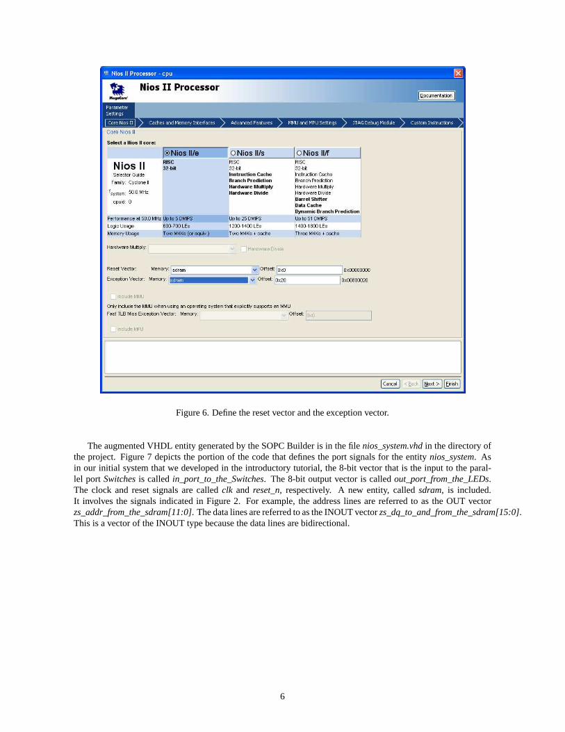
Figure 6. Define the reset vector and the exception vector.
The augmented VHDL entity generated by the SOPC Builder is inthe filenios_system.vhdin the directory ofthe project. Figure 7 depicts the portion of the code that defines the port signals for the entitynios_system. Asin our initial system that we developed in the introductory tutorial, the 8-bit vector that is the input to the paral-lel port Switchesis calledin_port_to_the_Switches. The 8-bit output vector is calledout_port_from_the_LEDs.The clock and reset signals are calledclk and reset_n, respectively. A new entity, calledsdram, is included.It involves the signals indicated in Figure 2. For example, the address lines are referred to as the OUT vectorzs_addr_from_the_sdram[11:0]. The data lines are referred to as the INOUT vectorzs_dq_to_and_from_the_sdram[15:0].This is a vector of the INOUT type because the data lines are bidirectional.
6

Figure 7. A part of the generated VHDL entity.
4 Integration of the Nios II System into the Quartus II Project
Now, we have to instantiate the expanded Nios II system in thetop-level VHDL entity, as we have done in thetutorial Introduction to the Altera SOPC Builder Using VHDL Design. The entity is namedlights, because this isthe name of the top-level design entity in our Quartus II project.
A first attempt at creating the new entity is presented in Figure 8. The input and output ports of the entity use thepin names for the 50-MHz clock,CLOCK_50, pushbutton switches,KEY, toggle switches,SW, and green LEDs,LEDG, as used in our original design. They also use the pin namesDRAM_CLK, DRAM_CKE, DRAM_ADDR,DRAM_BA_1, DRAM_BA_0, DRAM_CS_N, DRAM_CAS_N, DRAM_RAS_N, DRAM_WE_N, DRAM_DQ,DRAM_UDQM, andDRAM_LDQM, which correspond to the SDRAM signals indicated in Figure 2. All of thesenames are those specified in the DE2 User Manual, which allowsus to make the pin assignments by importingthem from the file calledDE2_pin_assignments.csvin the directoryDE2_tutorials\design_files, which is includedon the CD-ROM that accompanies the DE2 board and can also be found on Altera’s DE2 web pages.
Observe that the twoBank Addresssignals are treated by the SOPC Builder as a two-bit vector calledzs_ba_from_the_sdram[1:0], as seen in Figure 7. However, in theDE2_pin_assignments.csvfile these signalsare given as separate signalsDRAM_BA_1andDRAM_BA_0. This is accommodated by our VHDL code. Simi-larly, the vectorzs_dqm_from_the_sdram[1:0]corresponds to the signals(DRAM_UDQMandDRAM_LDQM).
Finally, note that we tried an obvious approach of using the 50-MHz system clock,CLOCK_50, as the clocksignal,DRAM_CLK, for the SDRAM chip. This is specified by the last assignment statement in the code. Thisapproach leads to a potential timing problem caused by the clock skew on the DE2 board, which can be fixed asexplained in section 5.
7

−− Inputs: SW7−0 are parallel port inputs to the Nios II system.−− CLOCK_50 is the system clock.−− KEY0 is the active-low system reset.−− Outputs: LEDG7−0 are parallel port outputs from the Nios II system.−− SDRAM ports correspond to the signals in Figure 2; their names are those−− used in the DE2 User Manual.LIBRARY ieee;USE ieee.std_logic_1164.all;USE ieee.std_logic_arith.all;USE ieee.std_logic_unsigned.all;
ENTITY lights ISPORT ( SW : IN STD_LOGIC_VECTOR(7 DOWNTO 0);
KEY : IN STD_LOGIC_VECTOR(0 DOWNTO 0);CLOCK_50 : IN STD_LOGIC;LEDG : OUT STD_LOGIC_VECTOR(7 DOWNTO 0)DRAM_CLK, DRAM_CKE : OUT STD_LOGIC;DRAM_ADDR : OUT STD_LOGIC_VECTOR(11 DOWNTO 0);DRAM_BA_1, DRAM_BA_0 : BUFFER STD_LOGIC;DRAM_CS_N, DRAM_CAS_N, DRAM_RAS_N, DRAM_WE_N : OUT STD_LOGIC;DRAM_DQ : INOUT STD_LOGIC_VECTOR(15 DOWNTO 0);DRAM_UDQM, DRAM_LDQM : BUFFER STD_LOGIC );
END lights;
ARCHITECTURE Structure OF lights ISCOMPONENT nios_system
PORT ( clk : IN STD_LOGIC;reset_n : IN STD_LOGIC;out_port_from_the_LEDs : OUT STD_LOGIC_VECTOR(7 DOWNTO 0);in_port_to_the_Switches : IN STD_LOGIC_VECTOR(7 DOWNTO 0)zs_addr_from_the_sdram : OUT STD_LOGIC_VECTOR(11 DOWNTO 0);zs_ba_from_the_sdram : BUFFER STD_LOGIC_VECTOR(1 DOWNTO 0);zs_cas_n_from_the_sdram : OUT STD_LOGIC;zs_cke_from_the_sdram : OUT STD_LOGIC;zs_cs_n_from_the_sdram : OUT STD_LOGIC;zs_dq_to_and_from_the_sdram : INOUT STD_LOGIC_VECTOR(15 DOWNTO 0);zs_dqm_from_the_sdram : BUFFER STD_LOGIC_VECTOR(1 DOWNTO0);zs_ras_n_from_the_sdram : OUT STD_LOGIC;zs_we_n_from_the_sdram : OUT STD_LOGIC );
END COMPONENT;SIGNAL BA : STD_LOGIC_VECTOR(1 DOWNTO 0);SIGNAL DQM : STD_LOGIC_VECTOR(1 DOWNTO 0);
BEGINDRAM_BA_1 <= BA(1); DRAM_BA_0 <= BA(0);DRAM_UDQM <= DQM(1); DRAM_LDQM <= DQM(0);
−− Instantiate the Nios II system entity generated by the SOPC Builder.NiosII: nios_system PORT MAP (CLOCK_50, KEY(0), LEDG, SW,
DRAM_ADDR, BA, DRAM_CAS_N, DRAM_CKE, DRAM_CS_N,DRAM_DQ, DQM, DRAM_RAS_N, DRAM_WE_N );
DRAM_CLK <= CLOCK_50;END Structure;
Figure 8. A first attempt at instantiating the expanded Nios II system.
8

As an experiment, you can enter the code in Figure 8 into a file calledlights.vhd. Add this file and all the *.vhdfiles produced by the SOPC Builder to your Quartus II project.Compile the code and download the design intothe Cyclone II FPGA on the DE2 board. Use the application program from the tutorialIntroduction to the AlteraSOPC Builder Using VHDL Design, which is shown in Figure 9. Notice in our expanded system, the addressesassigned by the SOPC Builder are 0x01003000 forSwitches and 0x01003010 forLEDs, which are different fromthe original system. These changes are already reflected in the program in Figure 9.
.include "nios_macros.s"
.equ Switches, 0x01003000
.equ LEDs, 0x01003010
.global _start_start:
movia r2, Switchesmovia r3, LEDs
loop: ldbio r4, 0(r2)stbio r4, 0(r3)br loop
Figure 9. Assembly language code to control the lights.
Use the Altera Monitor Program, which is described in the tutorial Altera Monitor Program, to assemble,download, and run this application program. If successful,the lights on the DE2 board will respond to the operationof the toggle switches.
Due to the clock skew problem mentioned above, the Nios II processor may be unable to properly access theSDRAM chip. A possible indication of this may be given by the Altera Monitor Program, which may display themessage depicted in Figure 10. To solve the problem, it is necessary to modify the design as indicated in the nextsection.
Figure 10. Error message in the Altera Monitor Program that may be due to the SDRAM clock skew problem.
5 Using a Phase-Locked Loop
The clock skew depends on physical characteristics of the DE2 board. For proper operation of the SDRAM chip,it is necessary that its clock signal,DRAM_CLK, leads the Nios II system clock,CLOCK_50, by 3 nanoseconds.
9

This can be accomplished by using aphase-locked loop (PLL)circuit. There exists a Quartus II Megafunction,calledALTPLL, which can be used to generate the desired circuit. The circuit can be created, by using the QuartusII MegaWizard Plug-In Manager, as follows:
1. SelectTools > MegaWizard Plug-In Manager. This leads to the window in Figure 11. Choose the actionCreate a new custom megafunction variation and clickNext.
Figure 11. The MegaWizard.
2. In the window in Figure 12, specify that Cyclone II is the device family used and that the circuit shouldbe defined in VHDL. Also, specify that the generated output (VHDL) file should be calledsdram_pll.vhd.From the list of megafunctions in the left box selectI/O > ALTPLL. Click Next.
Figure 12. Select the megafunction and name the output file.
3. In Figure 13, specify that the frequency of theinclock0 input is 50 MHz. Leave the other parameters asgiven by default. ClickNext to reach the window in Figure 14.
10

Figure 13. Define the clock frequency.
Figure 14. Remove unnecessary signals.
11

4. We are interested only in the input signalinclock0and the output signalc0. Remove the other two signalsshown in the block diagram in the figure by de-selecting the optional inputareset as well as thelockedoutput, as indicated in the figure. ClickNext on this page as well as on page 5, until you reach page 6which is shown in Figure 15.
Figure 15. Specify the phase shift.
5. The shifted clock signal is calledc0. Specify that the output clock frequency is 50 MHz. Also, specify thata phase shift of−3 ns is required, as indicated in the figure. ClickNext to reach the window in figure 16.
6. In order to ensure that the phase shift is exactly -3 ns, we will drive the original (non-shifted) clock throughthe PLL as well, but without any modifications. It will be called c1. SelectUse this clock and specifythat the output clock frequency is 50 MHz. Leave all the othersettings unchanged and clickFinish, whichadvances to page 10.
7. In the summary window in Figure 17 clickFinish to complete the process. At this point, a box may pop upasking you to add the newly generated files to the project. In this case, selectNo, since this is not neededwhen using VHDL.
12

Figure 16. Drive the original clock signal through the PLL.
13

Figure 17. The summary page.
The desired PLL circuit is now defined as a VHDL entity in the file sdram_pll.vhd, which is placed in the projectdirectory. Figure 18 shows the entity ports, consisting of signalsinclk0, c0, andc1.
Figure 18. The generated PLL entity.
14

Next, we have to fix the top-level VHDL entity, given in Figure8, to include the PLL circuit. The desiredcode is shown in Figure 19. The PLL circuit connects the shifted clock outputc0 to the pinDRAM_CLK, and theunmodified clock signalc1 to the clock signal required to drive the Nios II system.
−− Implements a simple Nios II system for the DE2 board.−− Inputs: SW7−0 are parallel port inputs to the Nios II system.−− CLOCK_50 is the system clock.−− KEY0 is the active-low system reset.−− Outputs: LEDG7−0 are parallel port outputs from the Nios II system.−− SDRAM ports correspond to the signals in Figure 2; their names are those−− used in the DE2 User Manual.LIBRARY ieee;USE ieee.std_logic_1164.all;USE ieee.std_logic_arith.all;USE ieee.std_logic_unsigned.all;
ENTITY lights ISPORT ( SW : IN STD_LOGIC_VECTOR(7 DOWNTO 0);
KEY : IN STD_LOGIC_VECTOR(0 DOWNTO 0);CLOCK_50 : IN STD_LOGIC;LEDG : OUT STD_LOGIC_VECTOR(7 DOWNTO 0)DRAM_CLK, DRAM_CKE : OUT STD_LOGIC;DRAM_ADDR : OUT STD_LOGIC_VECTOR(11 DOWNTO 0);DRAM_BA_1, DRAM_BA_0 : BUFFER STD_LOGIC;DRAM_CS_N, DRAM_CAS_N, DRAM_RAS_N, DRAM_WE_N : OUT STD_LOGIC;DRAM_DQ : INOUT STD_LOGIC_VECTOR(15 DOWNTO 0);DRAM_UDQM, DRAM_LDQM : BUFFER STD_LOGIC );
END lights;
ARCHITECTURE Structure OF lights ISCOMPONENT nios_system
PORT ( clk : IN STD_LOGIC;reset_n : IN STD_LOGIC;out_port_from_the_LEDs : OUT STD_LOGIC_VECTOR(7 DOWNTO 0);in_port_to_the_Switches : IN STD_LOGIC_VECTOR(7 DOWNTO 0)zs_addr_from_the_sdram : OUT STD_LOGIC_VECTOR(11 DOWNTO 0);zs_ba_from_the_sdram : BUFFER STD_LOGIC_VECTOR(1 DOWNTO 0);zs_cas_n_from_the_sdram : OUT STD_LOGIC;zs_cke_from_the_sdram : OUT STD_LOGIC;zs_cs_n_from_the_sdram : OUT STD_LOGIC;zs_dq_to_and_from_the_sdram : INOUT STD_LOGIC_VECTOR(15 DOWNTO 0);zs_dqm_from_the_sdram : BUFFER STD_LOGIC_VECTOR(1 DOWNTO0);zs_ras_n_from_the_sdram : OUT STD_LOGIC;zs_we_n_from_the_sdram : OUT STD_LOGIC );
END COMPONENT;
...continued in Partb
Figure 19. Proper instantiation of the expanded Nios II system (Parta).
15

COMPONENT sdram_pllPORT ( inclk0 : IN STD_LOGIC;
c0 : OUT STD_LOGIC );END COMPONENT
SIGNAL BA : STD_LOGIC_VECTOR(1 DOWNTO 0);SIGNAL DQM : STD_LOGIC_VECTOR(1 DOWNTO 0);
−− This signal is used to connect the unmodified clock signal c1 from the PLL to the−− NIOS II system
SIGNAL pll_c1 : STD_LOGIC;BEGIN
DRAM_BA_1 <= BA(1);DRAM_BA_0 <= BA(0);DRAM_UDQM <= DQM(1);DRAM_LDQM <= DQM(0);
−− Instantiate the Nios II system entity generated by the SOPC Builder.NiosII: nios_system PORT MAP (pll_c1, KEY(0), LEDG, SW,
DRAM_ADDR, BA, DRAM_CAS_N, DRAM_CKE, DRAM_CS_N,DRAM_DQ, DQM, DRAM_RAS_N, DRAM_WE_N );
−− Instantiate the entity sdram_pll (inclk0, c0).neg_3ns: sdram_pll PORT MAP (CLOCK_50, DRAM_CLK, pll_c1);
END Structure;
Figure 19. Proper instantiation of the expanded Nios II system (Partb).
Compile the code and download the design into the Cyclone II FPGA on the DE2 board. Use the applicationprogram in Figure 9 to test the circuit.
Copyright c©2008 Altera Corporation. All rights reserved. Altera, The Programmable Solutions Company, thestylized Altera logo, specific device designations, and allother words and logos that are identified as trademarksand/or service marks are, unless noted otherwise, the trademarks and service marks of Altera Corporation inthe U.S. and other countries. All other product or service names are the property of their respective holders.Altera products are protected under numerous U.S. and foreign patents and pending applications, mask workrights, and copyrights. Altera warrants performance of itssemiconductor products to current specifications inaccordance with Altera’s standard warranty, but reserves the right to make changes to any products and services atany time without notice. Altera assumes no responsibility or liability arising out of the application or use of anyinformation, product, or service described herein except as expressly agreed to in writing by Altera Corporation.Altera customers are advised to obtain the latest version ofdevice specifications before relying on any publishedinformation and before placing orders for products or services.This document is being provided on an “as-is” basis and as an accommodation and therefore all warranties, rep-resentations or guarantees of any kind (whether express, implied or statutory) including, without limitation, war-ranties of merchantability, non-infringement, or fitness for a particular purpose, are specifically disclaimed.
16