Using New Thermal Metrics - TI.com · R 9 R L1 R L2 R 2 R 2 R 6 R 8 R 5 R 7 R 3 R W1 R W1 R 4 R W2...
11
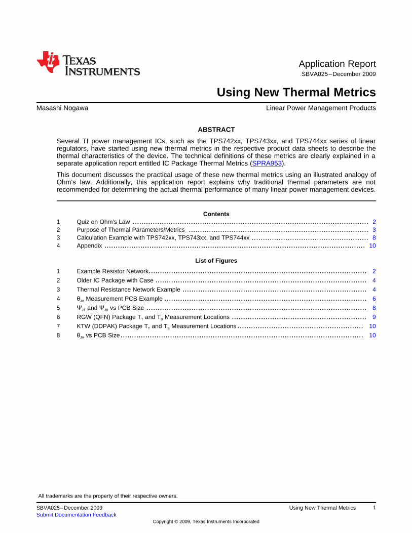
Application Report SBVA025 – December 2009 Using New Thermal Metrics Masashi Nogawa ............................................................................. Linear Power Management Products ABSTRACT Several TI power management ICs, such as the TPS742xx, TPS743xx, and TPS744xx series of linear regulators, have started using new thermal metrics in the respective product data sheets to describe the thermal characteristics of the device. The technical definitions of these metrics are clearly explained in a separate application report entitled IC Package Thermal Metrics (SPRA953). This document discusses the practical usage of these new thermal metrics using an illustrated analogy of Ohm's law. Additionally, this application report explains why traditional thermal parameters are not recommended for determining the actual thermal performance of many linear power management devices. Contents 1 Quiz on Ohm's Law ......................................................................................................... 2 2 Purpose of Thermal Parameters/Metrics ................................................................................ 3 3 Calculation Example with TPS742xx, TPS743xx, and TPS744xx .................................................... 8 4 Appendix .................................................................................................................... 10 List of Figures 1 Example Resistor Network................................................................................................. 2 2 Older IC Package with Case .............................................................................................. 4 3 Thermal Resistance Network Example .................................................................................. 4 4 θ JA Measurement PCB Example .......................................................................................... 6 5 Ψ JT and Ψ JB vs PCB Size .................................................................................................. 8 6 RGW (QFN) Package T T and T B Measurement Locations ............................................................ 9 7 KTW (DDPAK) Package T T and T B Measurement Locations ........................................................ 10 8 θ JA vs PCB Size ............................................................................................................ 10 All trademarks are the property of their respective owners. 1 SBVA025 – December 2009 Using New Thermal Metrics Submit Documentation Feedback Copyright © 2009, Texas Instruments Incorporated
Transcript of Using New Thermal Metrics - TI.com · R 9 R L1 R L2 R 2 R 2 R 6 R 8 R 5 R 7 R 3 R W1 R W1 R 4 R W2...
Application ReportSBVA025–December 2009
Using New Thermal MetricsMasashi Nogawa ............................................................................. Linear Power Management Products
ABSTRACT
Several TI power management ICs, such as the TPS742xx, TPS743xx, and TPS744xx series of linearregulators, have started using new thermal metrics in the respective product data sheets to describe thethermal characteristics of the device. The technical definitions of these metrics are clearly explained in aseparate application report entitled IC Package Thermal Metrics (SPRA953).
This document discusses the practical usage of these new thermal metrics using an illustrated analogy ofOhm's law. Additionally, this application report explains why traditional thermal parameters are notrecommended for determining the actual thermal performance of many linear power management devices.
Contents1 Quiz on Ohm's Law ......................................................................................................... 22 Purpose of Thermal Parameters/Metrics ................................................................................ 33 Calculation Example with TPS742xx, TPS743xx, and TPS744xx .................................................... 84 Appendix .................................................................................................................... 10
List of Figures
1 Example Resistor Network................................................................................................. 2
2 Older IC Package with Case .............................................................................................. 4
3 Thermal Resistance Network Example .................................................................................. 4
4 θJA Measurement PCB Example .......................................................................................... 6
5 ΨJT and ΨJB vs PCB Size .................................................................................................. 8
6 RGW (QFN) Package TT and TB Measurement Locations ............................................................ 9
7 KTW (DDPAK) Package TT and TB Measurement Locations ........................................................ 10
8 θJA vs PCB Size............................................................................................................ 10
All trademarks are the property of their respective owners.
1SBVA025–December 2009 Using New Thermal MetricsSubmit Documentation Feedback
Copyright © 2009, Texas Instruments Incorporated
R9
RL2RL1
R2
R2
R6
R8
R7R5
R3
RW1
RW1
R4
RW2
RJT R10
R11
RJP
A
T
J
P B2B1
(or C)
RJA
J
A
=
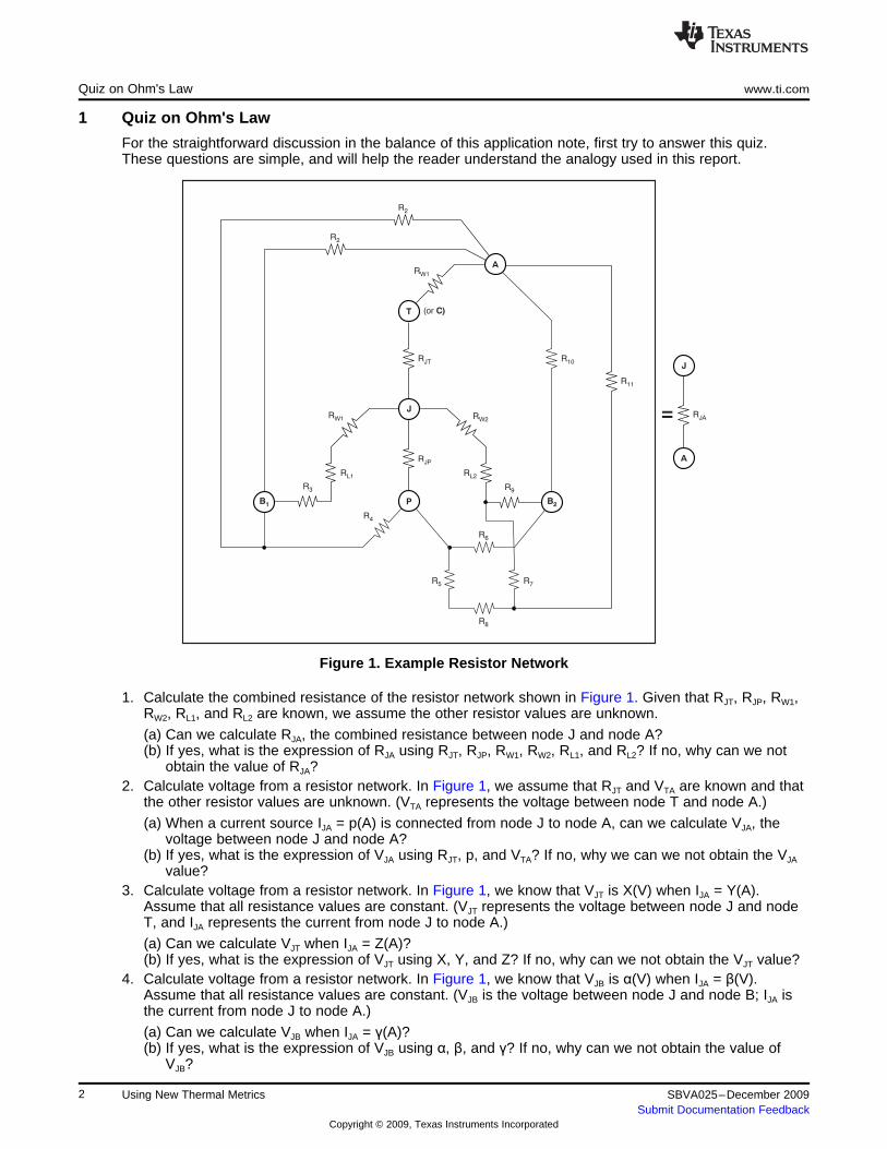
Quiz on Ohm's Law www.ti.com
1 Quiz on Ohm's Law
For the straightforward discussion in the balance of this application note, first try to answer this quiz.These questions are simple, and will help the reader understand the analogy used in this report.
Figure 1. Example Resistor Network
1. Calculate the combined resistance of the resistor network shown in Figure 1. Given that RJT, RJP, RW1,RW2, RL1, and RL2 are known, we assume the other resistor values are unknown.
(a) Can we calculate RJA, the combined resistance between node J and node A?(b) If yes, what is the expression of RJA using RJT, RJP, RW1, RW2, RL1, and RL2? If no, why can we not
obtain the value of RJA?2. Calculate voltage from a resistor network. In Figure 1, we assume that RJT and VTA are known and that
the other resistor values are unknown. (VTA represents the voltage between node T and node A.)
(a) When a current source IJA = p(A) is connected from node J to node A, can we calculate VJA, thevoltage between node J and node A?
(b) If yes, what is the expression of VJA using RJT, p, and VTA? If no, why we can we not obtain the VJA
value?3. Calculate voltage from a resistor network. In Figure 1, we know that VJT is X(V) when IJA = Y(A).
Assume that all resistance values are constant. (VJT represents the voltage between node J and nodeT, and IJA represents the current from node J to node A.)
(a) Can we calculate VJT when IJA = Z(A)?(b) If yes, what is the expression of VJT using X, Y, and Z? If no, why can we not obtain the VJT value?
4. Calculate voltage from a resistor network. In Figure 1, we know that VJB is α(V) when IJA = β(V).Assume that all resistance values are constant. (VJB is the voltage between node J and node B; IJA isthe current from node J to node A.)
(a) Can we calculate VJB when IJA = γ(A)?(b) If yes, what is the expression of VJB using α, β, and γ? If no, why can we not obtain the value of
VJB?
2 Using New Thermal Metrics SBVA025–December 2009Submit Documentation Feedback
Copyright © 2009, Texas Instruments Incorporated
www.ti.com Purpose of Thermal Parameters/Metrics
2 Purpose of Thermal Parameters/Metrics
2.1 Objective
The ideal target of thermal management in a new design is to ensure that every silicon device on theboard works within its allowable operating junction temperature. More specifically, thermal managementattempts to ensure that the IC works within the specifications of the operating maximum junctiontemperature, or TJ(max). Keep in mind that most IC devices define an absolute maximum junctiontemperature as well as an operating maximum junction temperature. Because the parameter absolutemaximum temperature defines the thermal point at which the device is damaged, we must refer in thisdocument to the operating maximum temperature, TJ, which defines the maximum allowable temperaturefor continuous normal operation of the device.
The greatest difficulty we face in order to achieve this target is that there is no direct way to measure TJ byusing a thermocouple or infrared thermometer, because the IC is covered with a mold compound and theactual junction is not exposed. For many large package ICs, such as PC processors or PC graphicsprocessors, there is a built-in function to measure TJ using integrated thermosensors, which in turn providea read-out to an analog-to-digital (A/D) converter. For small package ICs, however—including most powerICs—there is no such TJ sensor function as a result of silicon size and package pin count limitations.Consequently, we must estimate TJ by thermal calculation and thermal evaluation.
2.2 A Practical Method to Estimate Junction Temperature
On every application board, it is a reasonable, fair, and valid assumption that we can measure severaltemperature points. The highlighted single letter in each row refers to parameters discussed later in thisreport.
Parameter Definition/Measurement Point
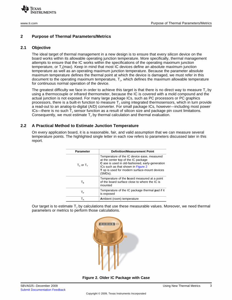
Temperature of the IC device case, measuredat the center top of the IC packageC ase is used in old-fashioned, early-generationTC or TT ICs such as that shown in Figure 2T op is used for modern surface-mount devices(SMDs).
Temperature of the board measured at a pointTB of the board surface close to where the IC is
mounted
Temperature of the IC package thermal pad if itTP is exposed
TA Ambient (room) temperature
Our target is to estimate TJ by calculations that use these measurable values. Moreover, we need thermalparameters or metrics to perform those calculations.
Figure 2. Older IC Package with Case
3SBVA025–December 2009 Using New Thermal MetricsSubmit Documentation Feedback
Copyright © 2009, Texas Instruments Incorporated
J
A
=
A
(or C)
Mold Compound (Epoxy) Leadframe Die Pad
Exposed at Base of the Package
Leadframe (Copper Alloy)
IC (Silicon)Die Attach (Epoxy)
qJC
qJP
T
J
P
Solder BallSolder Paste
B2B1 Copper Layer (Top)
Copper Layer #2
Copper Layer #3
Copper Layer #4
Copper Layer (Bottom)
Purpose of Thermal Parameters/Metrics www.ti.com
2.3 Why Not θJC or θJA?
By answering each question presented in Section 1, we can explain why TI recommends that designersnot use θJC or θJA. This section also explains why TI advises designers to use the set of new thermalmetrics, ΨJB and ΨJT.
2.3.1 Analogy of Electrical and Thermal Resistance
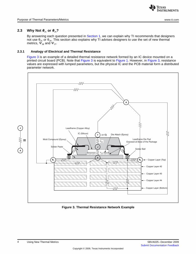
Figure 3 is an example of a detailed thermal resistance network formed by an IC device mounted on aprinted circuit board (PCB). Note that Figure 3 is equivalent to Figure 1. However, in Figure 3, resistancevalues are expressed with lumped parameters, but the physical IC and the PCB material form a distributedparameter network.
Figure 3. Thermal Resistance Network Example
4 Using New Thermal Metrics SBVA025–December 2009Submit Documentation Feedback
Copyright © 2009, Texas Instruments Incorporated
R( ) =WE (V)
I (A)
Temperature ( C)
Power (W)
°R ( /W) =
qC°
www.ti.com Purpose of Thermal Parameters/Metrics
In the world of electronics and electrical design, resistance value is defined by Ohm's law:
(1)
The electrical resistance shows a ratio of how much electrical potential difference is caused by (electron)current flow.
In the thermal world, though, resistance is defined by this equation:
(2)
Thermal resistance shows a ratio of how much temperature difference is caused by power (heat) flow.
2.4 Quiz Answers
Now let us consider the answers to the quiz given in Section 1.
2.4.1 Question #1
Answer: No
We have too little information to calculate the combination resistance.
To calculate a combination resistance, we need to know all resistor values.
Comparing Figure 1 and Figure 3, RJT, RJP, RW1, RW2, RL1, and RL2 are all lumped parameter resistanceswithin the IC. This question shows us that in the thermal world, θJA cannot be determined only by the IC. Itdepends greatly on the application board. Every different PCB has a different θJA value. The primaryconcern to most IC designers is what happens on their own application boards, so using θJA is notrecommended.
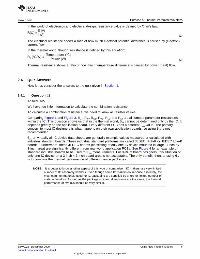
θJA on virtually all IC device data sheets are generally example values measured or calculated withindustrial standard boards. These industrial standard platforms are called JEDEC High-K or JEDEC Low-Kboards. Furthermore, these JEDEC boards (consisting of only one IC device mounted in large, 3-inch by3-inch area) are significantly different from real-world application PCBs. See Figure 4 for an example ofstandard industrial boards to be used for θJA measurements. For 99% of board designers, this situation ofonly one IC device on a 3-inch × 3-inch board area is not acceptable. The only benefit, then, to using θJA
is to compare the thermal performance of different device packages.
NOTE: It is better to know another aspect of this type of comparison: IC makers use very limitednumber of IC assembly vendors. Even though some IC makers do in-house assembly, themost common materials used for IC packaging are supplied by a further limited number ofmaterial vendors. As long as the package size and dimensions are the same, the thermalperformance of two ICs should be very similar.
5SBVA025–December 2009 Using New Thermal MetricsSubmit Documentation Feedback
Copyright © 2009, Texas Instruments Incorporated
Purpose of Thermal Parameters/Metrics www.ti.com
Figure 4. θJA Measurement PCB Example
2.4.2 Question #2
Answer: No
Again, we have too little information, in this case to solve a matrix of Kirchhoff's circuit law.
To calculate the target voltage, we need to know all other resistor values because the current IJA is goingthrough every possible path. In this question, the availability of RJA is intentionally excluded because theanswer for the first question shows that a typical RJA value does not necessarily represent a real-worldapplication board for most IC device designers. Additionally, using RJA very quickly gives us a falseanswer:
VJA = RJA × IJA
Let's turn to the thermal world.
In the earlier days of IC devices, using an IC package such as Figure 2 shows, it was a good assumptionthat the majority of power (heat) dissipated from the surface between the IC case and ambient air. Thisassumption was based on the fact that the IC package was almost always isolated from the PCB; inanother words, the IC was in effect floating on the PCB. In terms of typical measurement, then, RJC isextremely small compared to the other resistance values, and the majority of heat flows through RJC (thispractical result is actually the definition of θJC in the JEDEC standard). When RJC is very small and theother resistors can be ignored, the following formula becomes valid:
RJA ≈ RJC + RCA
This equation illustrates that using θJA and θJC could solve most thermal calculations in those days; abackwards-compatibility to this historical perspective is probably the only reason IC makers continue touse θJA and θJC.
In contemporary IC manufacturing, SMDs dissipate the majority of heat to the board. It should be evidentfrom this question that θJC does not give any meaningful information about TJ.
6 Using New Thermal Metrics SBVA025–December 2009Submit Documentation Feedback
Copyright © 2009, Texas Instruments Incorporated
V =JT
X
Y· Z
Y =JT
X
Y
T = T + PYJ T JT D
·
V =JB
ab
· g
T = T + PYJ B JB D
·
www.ti.com Purpose of Thermal Parameters/Metrics
2.4.3 Question #3
Answer: Yes
We expect linearity, VJT to be given in this manner:
(3)
In our thermal discussion, this question shows an opportunity to easily estimate TJ; the only step requiredis to figure out a constant:
These days, we have very good thermal simulators to calculate this constant, ΨJT; finding the value is notan issue. The relevant point here is the dependency of this constant to the PCB as with our discussion inthe previous answer to question #2. In contrast, the fact that SMDs dissipate the majority of heat to thePCB helps the situation. When most of the device heat goes into the board, there is a very low heat flowthrough θJT, so the temperature difference between TJ and TT should be very small. That slight differencemeans that the value of the constant ΨJT should be very small. If it is small, then any error caused byboard variation is small, too.
This constant represents one of the new thermal metrics, ΨJT.
By knowing TT, we can estimate TJ using Equation 4, where PD is the power loss at a silicon junction.
(4)
2.4.4 Question #4
Answer: Yes
We expect linearity, VJB, to be given in this manner:
(5)
Comparing the answers to questions 3 and 4, we can have a very similar discussion.
The difference between these answers is a discussion of the error caused by board variation. A path fromthe junction to the board consists of all metal: silicon and aluminum comprise the IC routing layer; thebonding wire is often gold; the IC lead consists of copper, as does the solder paste; and the PCB patternalso contains metal. Therefore, the combined thermal resistance from junction-to-board is very small. As aresult, again, if this thermal resistance is small, the error is small, as well.
This result also generates the other new thermal metric, ΨJB.
By knowing TB, we can estimate TJ with Equation 6, where PD is the power loss at a silicon junction.
(6)
7SBVA025–December 2009 Using New Thermal MetricsSubmit Documentation Feedback
Copyright © 2009, Texas Instruments Incorporated
12
10
8
6
4
2
0
YY
and
(C
/W)
JT
JB
°
0 2 4 6 8 10
Board Size (in )2
YJT (KTW)
YJT (RGW)
YJB (RGW)
YJB (KTW)
Y YJT JBAND VERSUS PCB SIZE
P = (V V ) I-D IN OUT OUT·
Calculation Example with TPS742xx, TPS743xx, and TPS744xx www.ti.com
3 Calculation Example with TPS742xx, TPS743xx, and TPS744xx
In the current revisions of the product data sheets for the TPS742xx, TPS743xx, and TPS744xx series oflow-dropout linear regulators, TI introduces ΨJT and ΨJB. Consider the TPS74401KTW as we look at anillustration of how to use these new thermal metrics.
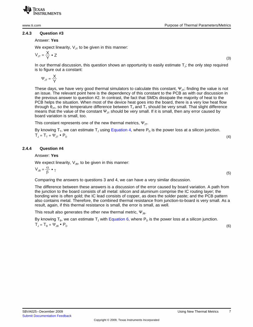
Step 1. Calculate ΨJT and ΨJB from a graph.
Figure 5. ΨJT and ΨJB vs PCB Size
By looking at Figure 5 from the TPS744xx data sheet, we can identify proper ΨJT and ΨJB valuesdepending on the target application board size. The board size to be used here is the area of the PCBassigned only for the TPS74401 IC device. This area can include passive components as long asthose components are not a heat source, but any other IC devices are not included.In this example, assume the board size is 2-in2. Select ΨJT = 4.5°C/W and ΨJB = 6.3°C/W.spaceStep 2. Calculate PD.Calculate the power dissipation using Equation 7.
(7)
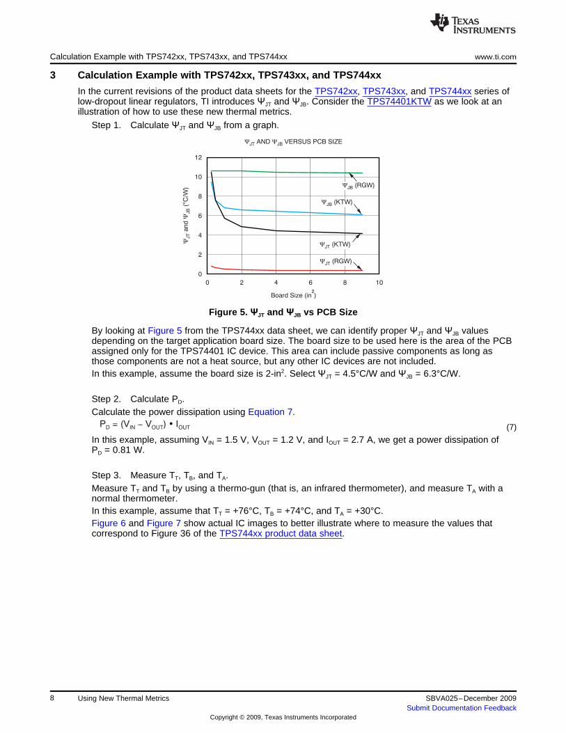
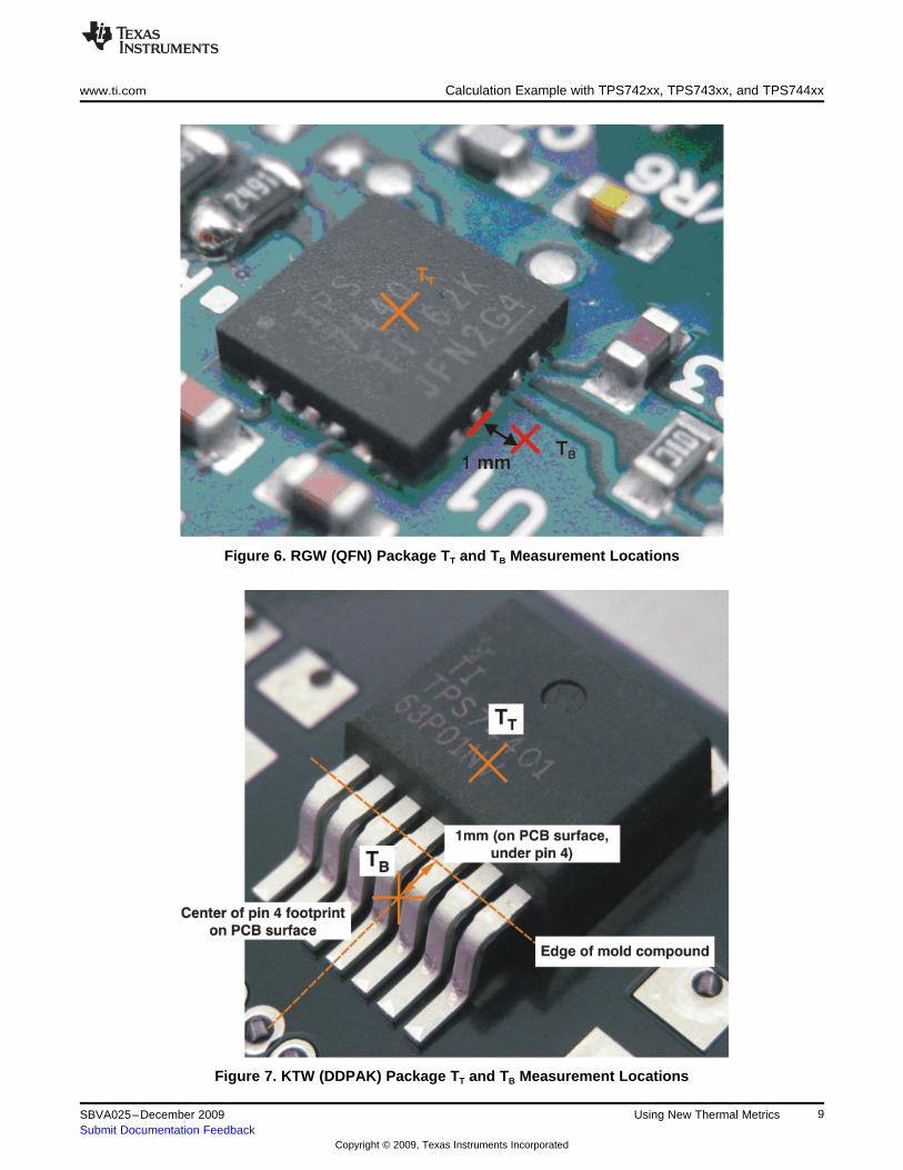
In this example, assuming VIN = 1.5 V, VOUT = 1.2 V, and IOUT = 2.7 A, we get a power dissipation ofPD = 0.81 W.spaceStep 3. Measure TT, TB, and TA.Measure TT and TB by using a thermo-gun (that is, an infrared thermometer), and measure TA with anormal thermometer.In this example, assume that TT = +76°C, TB = +74°C, and TA = +30°C.Figure 6 and Figure 7 show actual IC images to better illustrate where to measure the values thatcorrespond to Figure 36 of the TPS744xx product data sheet.
8 Using New Thermal Metrics SBVA025–December 2009Submit Documentation Feedback
Copyright © 2009, Texas Instruments Incorporated
www.ti.com Calculation Example with TPS742xx, TPS743xx, and TPS744xx
Figure 6. RGW (QFN) Package TT and TB Measurement Locations
Figure 7. KTW (DDPAK) Package TT and TB Measurement Locations
9SBVA025–December 2009 Using New Thermal MetricsSubmit Documentation Feedback
Copyright © 2009, Texas Instruments Incorporated
T = T + P = 76 + 4.5 0.81 = 79.6 CYJ T JT D
· °·
T = T + P = 74 + 6.3 0.81 = 79.1 CYJ B JB D
· °·
120
100
80
60
40
20
0
qJA
(C
/W)
°
0 1 2 3 4 5 6 7 8 9 10
Board Size (in )2
qJA (KTW)
qJA (RGW)
q VERSUS PCB SIZEJA
Appendix www.ti.com
Step 4. Estimate TJ.Now apply Step 3 to Equation 1 and Equation 2.In this example, two TJ estimations can be said to be close enough.
(8)
(9)
Step 5. Validate the estimated TJ value.Compare the results from Equation 8 and Equation 9. The TJ temperature estimates from these twoequations should be very close. If these estimated values are close, we can accept that we have areasonable TJ value; if these estimates are not aligned, however, we must check for something thatcould cause an error.
3.1 Key Points of This Example Study
We can summarize our discussion with these conclusions:
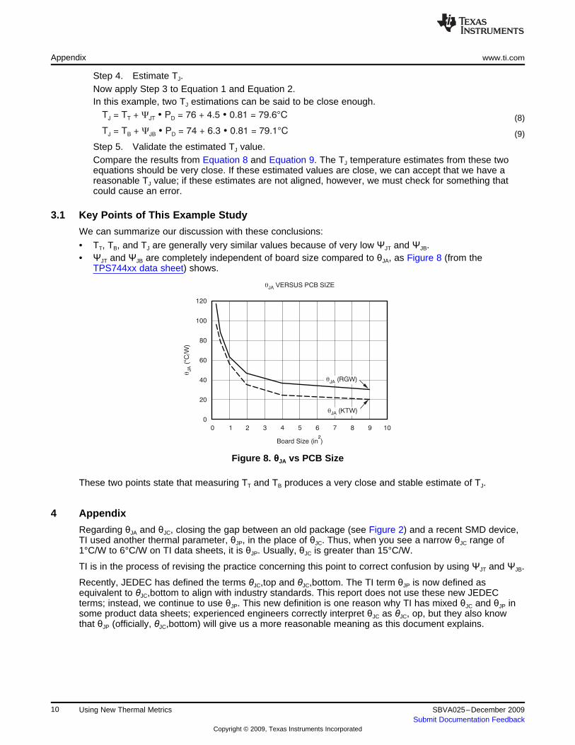
• TT, TB, and TJ are generally very similar values because of very low ΨJT and ΨJB.• ΨJT and ΨJB are completely independent of board size compared to θJA, as Figure 8 (from the
TPS744xx data sheet) shows.
Figure 8. θJA vs PCB Size
These two points state that measuring TT and TB produces a very close and stable estimate of TJ.
4 Appendix
Regarding θJA and θJC, closing the gap between an old package (see Figure 2) and a recent SMD device,TI used another thermal parameter, θJP, in the place of θJC. Thus, when you see a narrow θJC range of1°C/W to 6°C/W on TI data sheets, it is θJP. Usually, θJC is greater than 15°C/W.
TI is in the process of revising the practice concerning this point to correct confusion by using ΨJT and ΨJB.
Recently, JEDEC has defined the terms θJC,top and θJC,bottom. The TI term θJP is now defined asequivalent to θJC,bottom to align with industry standards. This report does not use these new JEDECterms; instead, we continue to use θJP. This new definition is one reason why TI has mixed θJC and θJP insome product data sheets; experienced engineers correctly interpret θJC as θJC, op, but they also knowthat θJP (officially, θJC,bottom) will give us a more reasonable meaning as this document explains.
10 Using New Thermal Metrics SBVA025–December 2009Submit Documentation Feedback
Copyright © 2009, Texas Instruments Incorporated
IMPORTANT NOTICETexas Instruments Incorporated and its subsidiaries (TI) reserve the right to make corrections, modifications, enhancements, improvements,and other changes to its products and services at any time and to discontinue any product or service without notice. Customers shouldobtain the latest relevant information before placing orders and should verify that such information is current and complete. All products aresold subject to TI’s terms and conditions of sale supplied at the time of order acknowledgment.TI warrants performance of its hardware products to the specifications applicable at the time of sale in accordance with TI’s standardwarranty. Testing and other quality control techniques are used to the extent TI deems necessary to support this warranty. Except wheremandated by government requirements, testing of all parameters of each product is not necessarily performed.TI assumes no liability for applications assistance or customer product design. Customers are responsible for their products andapplications using TI components. To minimize the risks associated with customer products and applications, customers should provideadequate design and operating safeguards.TI does not warrant or represent that any license, either express or implied, is granted under any TI patent right, copyright, mask work right,or other TI intellectual property right relating to any combination, machine, or process in which TI products or services are used. Informationpublished by TI regarding third-party products or services does not constitute a license from TI to use such products or services or awarranty or endorsement thereof. Use of such information may require a license from a third party under the patents or other intellectualproperty of the third party, or a license from TI under the patents or other intellectual property of TI.Reproduction of TI information in TI data books or data sheets is permissible only if reproduction is without alteration and is accompaniedby all associated warranties, conditions, limitations, and notices. Reproduction of this information with alteration is an unfair and deceptivebusiness practice. TI is not responsible or liable for such altered documentation. Information of third parties may be subject to additionalrestrictions.Resale of TI products or services with statements different from or beyond the parameters stated by TI for that product or service voids allexpress and any implied warranties for the associated TI product or service and is an unfair and deceptive business practice. TI is notresponsible or liable for any such statements.TI products are not authorized for use in safety-critical applications (such as life support) where a failure of the TI product would reasonablybe expected to cause severe personal injury or death, unless officers of the parties have executed an agreement specifically governingsuch use. Buyers represent that they have all necessary expertise in the safety and regulatory ramifications of their applications, andacknowledge and agree that they are solely responsible for all legal, regulatory and safety-related requirements concerning their productsand any use of TI products in such safety-critical applications, notwithstanding any applications-related information or support that may beprovided by TI. Further, Buyers must fully indemnify TI and its representatives against any damages arising out of the use of TI products insuch safety-critical applications.TI products are neither designed nor intended for use in military/aerospace applications or environments unless the TI products arespecifically designated by TI as military-grade or "enhanced plastic." Only products designated by TI as military-grade meet militaryspecifications. Buyers acknowledge and agree that any such use of TI products which TI has not designated as military-grade is solely atthe Buyer's risk, and that they are solely responsible for compliance with all legal and regulatory requirements in connection with such use.TI products are neither designed nor intended for use in automotive applications or environments unless the specific TI products aredesignated by TI as compliant with ISO/TS 16949 requirements. Buyers acknowledge and agree that, if they use any non-designatedproducts in automotive applications, TI will not be responsible for any failure to meet such requirements.Following are URLs where you can obtain information on other Texas Instruments products and application solutions:Products ApplicationsAmplifiers amplifier.ti.com Audio www.ti.com/audioData Converters dataconverter.ti.com Automotive www.ti.com/automotiveDLP® Products www.dlp.com Broadband www.ti.com/broadbandDSP dsp.ti.com Digital Control www.ti.com/digitalcontrolClocks and Timers www.ti.com/clocks Medical www.ti.com/medicalInterface interface.ti.com Military www.ti.com/militaryLogic logic.ti.com Optical Networking www.ti.com/opticalnetworkPower Mgmt power.ti.com Security www.ti.com/securityMicrocontrollers microcontroller.ti.com Telephony www.ti.com/telephonyRFID www.ti-rfid.com Video & Imaging www.ti.com/videoRF/IF and ZigBee® Solutions www.ti.com/lprf Wireless www.ti.com/wireless
Mailing Address: Texas Instruments, Post Office Box 655303, Dallas, Texas 75265Copyright © 2009, Texas Instruments Incorporated