University - UM
101
DESIGN OF WIDEBAND POWER AMPLIFIER FOR GAN HEMT FOR RADIO APPLICATION LIM WEN JUN FACULTY OF ENGINEERING UNIVERSITY OF MALAYA KUALA LUMPUR 2017 University of Malaya
Transcript of University - UM

DESIGN OF WIDEBAND POWER AMPLIFIER FOR GAN HEMT FOR RADIO APPLICATION
LIM WEN JUN
FACULTY OF ENGINEERING
UNIVERSITY OF MALAYA KUALA LUMPUR
2017Univ
ersity
of M
alaya

DESIGN OF WIDEBAND POWER AMPLIFIER FOR
GAN HEMT FOR RADIO APPLICATION
LIM WEN JUN
DISSERTATION SUBMITTED IN FULFILMENT OF
THE REQUIREMENTS FOR THE DEGREE OF MASTER
OF ENGINEERING SCIENCE
FACULTY OF ENGINEERING
UNIVERSITY OF MALAYA
KUALA LUMPUR
2017 Univers
ityof
Malaya

ii
UNIVERSITY OF MALAYA
ORIGINAL LITERARY WORK DECLARATION
Name of Candidate: Lim Wen Jun
Matric No: KGA140060
Name of Degree: Master in Engineering Science
Title of Project Paper/Research Report/Dissertation/Thesis (“this Work”):
Design of Wideband Power Amplifier for GaN HEMT for Radio Application
Field of Study: Electronics
I do solemnly and sincerely declare that:
(1) I am the sole author/writer of this Work;
(2) This Work is original;
(3) Any use of any work in which copyright exists was done by way of fair dealing
and for permitted purposes and any excerpt or extract from, or reference to or
reproduction of any copyright work has been disclosed expressly and
sufficiently and the title of the Work and its authorship have been
acknowledged in this Work;
(4) I do not have any actual knowledge nor do I ought reasonably to know that the
making of this work constitutes an infringement of any copyright work;
(5) I hereby assign all and every rights in the copyright to this Work to the
University of Malaya (“UM”), who henceforth shall be owner of the copyright
in this Work and that any reproduction or use in any form or by any means
whatsoever is prohibited without the written consent of UM having been first
had and obtained;
(6) I am fully aware that if in the course of making this Work I have infringed any
copyright whether intentionally or otherwise, I may be subject to legal action
or any other action as may be determined by UM.
Candidate’s Signature Date:
Subscribed and solemnly declared before,
Witness’s Signature Date:
Name:
Designation:
Univers
ity of
Mala
ya

iii
ABSTRACT
In the field of communication, the vast developing of the communication system in
past decades that changes the way of interaction between mankind. In this thesis, the focus
has been given to the design of single system where it can operate at wideband frequency
in simplest circuit and enhanced performances. In this project, a wideband power
amplifier (PA) is designed using real frequency technique (RFT). The motivation of this
project is to show that by using the idea of RFT and practical implementation of
distributed elements and lumped elements (mixed-lumped elements design), the PA
designed is able to achieve satisfying results with wide bandwidth range of 80 MHz to
2200 MHz. The measurement results reported good performance over the bandwidth of
the interest (i.e. power of 41 dBm, efficiency about 67% and gain more than 13 dB), and
reasonable agreement with the simulated data. The results are significant for single-ended
GaN HEMT device for the wideband operation starting from low frequency 80 –
2200 MHz.
Univers
ity of
Malaya

iv
ABSTRAK
Beberapa tahun kebelakangan ini, perkembangan pesat dalam bidang komunikasi telah
mengubah cara interaksi di antara manusia. Dalam thesis ini, tumpuan diberikan dalam
merekabentuk sistem tunggal yang beroperasi pada frekuensi jalur lebar dengan litar yang
paling mudah dan menambahbaikkan prestasi. Dalam kajian ini, sebuah penguat kuasa
berjalur lebar di rekabentuk menggunakan ‘Real Frequency Technique’ (RFT). Motivasi
dalam kajian ini adalah untuk membuktikan dengan menggunakan kaedah RFT dan
pelaksanaan praktikal unsur diedarkan dan unsur tergumpal (rekabentuk unsur tergumpal
campuran). Penguat kuasa yang direka tersebut boleh mencapai keputusan yang
memuaskan dengan lebar jalur di antara 80 MHz ke 2200 MHz. Keputusan pengukuran
menunjukkan prestasi yang baik mengatasi lebar jalur terpilih (contoh: kuasa 41 dBm,
kecekapan 67% dan keuntungan melebihi dari 13 dB), dan menyetujui dengan data
simulasi. Keputusan tersebut adalah sangat ketara untuk peranti tunggal-akhir GaN
HEMT untuk operasi jalur lebar bermula frekuensi 80 – 2200 MHz.
Univers
ity of
Mala
ya

v
ACKNOWLEDGEMENTS
First of all, I would like to express my gratitude towards my supervisor, Dr. Narendra
Kumar for provide the endless support and guidance throughout this project. His kindness
and encouragement always inspired me to do my best for this work. I am very grateful to
my supervisor for all the kind help and patience advice all the while.
I would also like to acknowledge Motorola Solutions, the main collaborator and supporter
of this project in terms of funding. I would like to acknowledge CREST for the help of
financial management. I also would like to express my appreciation to the companies and
vendors who providing us the components or services for prototype development. I would
like to thanks my project partner Ms. Huan Hui Yan who helped me a lot in terms of
technical writing, component purchasing and experiment equipment setup so that my
project can be carried out smoothly.
Finally, I would like to thank my parents for their unconditional love and support. They
supported me spiritually whenever I felt like giving up. Their love and support inspired
me to strive for the best.
Univers
ity of
Mala
ya

vi
TABLE OF CONTENTS
Abstract ............................................................................................................................ iii
Abstrak ............................................................................................................................. iv
Acknowledgements ........................................................................................................... v
Table of Contents ............................................................................................................. vi
List of Figures .................................................................................................................. ix
List of Tables.................................................................................................................... xi
List of Symbols and Abbreviations ................................................................................. xii
CHAPTER 1: INTRODUCTION .................................................................................. 1
1.1 Background .............................................................................................................. 1
1.2 Problem statement ................................................................................................... 2
1.3 Research aim ............................................................................................................ 2
1.4 Objectives ................................................................................................................ 3
1.5 Organization of Dissertation .................................................................................... 4
CHAPTER 2: LITERATURE REVIEW ...................................................................... 5
2.1 Introduction of Power Amplifier ............................................................................. 5
2.1.1 Power Amplifier Basics .............................................................................. 5
2.1.2 Power Amplifier Classification .................................................................. 5
2.1.2.1 Transconductance PA .................................................................. 5
2.1.2.2 Switch Mode PA ......................................................................... 7
2.1.3 Recent works in PA design ........................................................................ 9
2.2 Power Amplifier Figures-of-Merits ....................................................................... 10
2.2.1 Efficiency ................................................................................................. 10
2.2.1.1 Drain Efficiency ........................................................................ 11
Univers
ity of
Mala
ya

vii
2.2.1.2 Power Added Efficiency (PAE) ................................................ 11
2.2.2 Gain .......................................................................................................... 12
2.2.3 Output power ............................................................................................ 14
2.3 S-parameter ............................................................................................................ 15
2.4 Broadband Impedance matching ........................................................................... 19
2.5 Coplanar Waveguide with Ground (CPWG) ......................................................... 23
2.5.1 Introduction of CPWG ............................................................................. 23
2.5.2 Advantages of CPWG compared to microstrip ........................................ 23
2.6 Real Frequency Technique .................................................................................... 24
2.6.1 Background .............................................................................................. 24
2.6.2 Theory of Real Frequency Technique ...................................................... 26
2.7 Summary ................................................................................................................ 29
CHAPTER 3: METHODOLOGY ............................................................................... 31
3.1 Design of matching network .................................................................................. 31
3.1.1 Initial Guess Technique ............................................................................ 31
3.1.2 Initial Guess Simulation using MATLAB ................................................ 31
3.2 Mixed-lumped and distributed elements implementation ..................................... 36
3.2.1 Distributed and Lumped elements ............................................................ 36
3.2.2 Mixed Lumped and distributed elements matching network ................... 37
3.2.3 CPWG Implementation ............................................................................ 38
3.2.4 Capacitor implementation ........................................................................ 42
3.3 DC Biasing Circuit ................................................................................................ 44
3.4 Advance Design System (ADS) Simulation .......................................................... 47
3.4.1 Simulation of Matching Network with Mixed-Lumped Design .............. 47
3.4.2 3.5.2 Simulation of Complete PA Circuit ................................................ 48
3.5 PCB layout Design ................................................................................................ 49
Univers
ity of
Mala
ya

viii
3.5.1 Layout Construction using OrCAD CIS Capture Software ..................... 49
3.5.2 Footprint construction for Each Component ............................................ 50
3.5.3 Layout Design .......................................................................................... 51
3.6 Heat Sink Design ................................................................................................... 53
3.7 PCB Fabrication..................................................................................................... 55
3.8 Measurement Setup ............................................................................................... 58
3.9 Summary ................................................................................................................ 59
CHAPTER 4: RESULTS AND DISCUSSION .......................................................... 60
4.1 Matching Network Development .......................................................................... 60
4.2 Mixed-Lumped Element Implementation.............................................................. 63
4.2.1 CPWG Parameter Selection ..................................................................... 64
4.2.2 ATC Capacitor Implementation ............................................................... 66
4.3 Simulation Results ................................................................................................. 67
4.3.1 Simulation of Matching Networks with Mixed-Lumped Design ............. 68
4.3.2 4.3.2 Simulation of GaN HEMT PA ........................................................ 71
4.4 Measurement Results ............................................................................................. 76
4.5 Comparison of performances with various works ................................................. 80
4.6 Summary ................................................................................................................ 81
CHAPTER 5: CONCLUSION ..................................................................................... 82
5.1 Conclusion ............................................................................................................. 82
5.2 Future Work ........................................................................................................... 82
References ....................................................................................................................... 84
List of Publications and Papers Presented ...................................................................... 87
Univers
ity of
Mala
ya

ix
LIST OF FIGURES
Figure 2.1: The generic schematic of a power amplifier .................................................. 5
Figure 2.2: The reduced conduction angle current waveform .......................................... 6
Figure 2.3: Basic circuit of Class-E power amplifier ........................................................ 8
Figure 2.4: Class-F power amplifier using a quarter-wave transmission line................... 9
Figure 2.5: General two-port network with characteristic impedance Zo ....................... 17
Figure 2.6: Source and load impedance circuit ............................................................... 20
Figure 2.7: Impedance matching equalizer network ....................................................... 21
Figure 2.8: Simplified diagram of CPWG ...................................................................... 23
Figure 2.9: Lossless matching network in terms of Darlington’s driving point impedance.
......................................................................................................................................... 26
Figure 3.1: Command window for parameter insertion .................................................. 32
Figure 3.2: Example of matching network obtained from execution of RFT algorithm 35
Figure 3.3: TPG against frequency for matching network obtained from RFT algorithm
......................................................................................................................................... 36
Figure 3.4: LineCalc tool interface for the synthesis of l and w ..................................... 40
Figure 3.5: Schematic of S-parameter conversion of 2-port to 1-port ............................ 41
Figure 3.6: Schematic circuit for capacitor simulation ................................................... 43
Figure 3.7: Simulation result of the capacitors ............................................................... 43
Figure 3.8: Basic DC biasing circuit ............................................................................... 44
Figure 3.9: Basic DC biasing circuit ............................................................................... 46
Figure 3.10: Graph of current against voltage for GaN biasing ...................................... 46
Figure 3.11: Construction of IMN with mixed-lump design .......................................... 47
Figure 3.12: PA circuit construction in ADS .................................................................. 48
Figure 3.13: Schematic circuit construction on CIS Capture tool .................................. 49
Univers
ity of
Mala
ya

x
Figure 3.14: PCB layout of the PA design ...................................................................... 52
Figure 3.15: Heat Sink Layout Top View ....................................................................... 53
Figure 3.16: Heat Sink Layout Side View ...................................................................... 53
Figure 3.17: PCB fabrication by Brusia Engineering Sdn Bhd ...................................... 56
Figure 3.18: Complete PA PCB (top view) .................................................................... 57
Figure 3.19: Complete PA PCB with heat sink (side view) ............................................ 57
Figure 3.20: Experiment setup for data measurement .................................................... 58
Figure 4.1: Schematic circuit for IMN ............................................................................ 61
Figure 4.2: Graph of TPG against frequency for IMN.................................................... 61
Figure 4.3: Schematic circuit for OMN .......................................................................... 62
Figure 4.4: Graph of TPG against frequency for OMN .................................................. 63
Figure 4.5: Schematic circuit of IMN with mixed-lumped design ................................. 68
Figure 4.6: Graph of TPG against frequency for IMN with mixed-lumped design ........ 69
Figure 4.7: Schematic circuit of OMN with mixed-lumped design ................................ 69
Figure 4.8: Graph of TPG against frequency for OMN with mixed-lumped design ...... 70
Figure 4.9: Complete schematic circuit of GaN PA ....................................................... 71
Figure 4.10: Graph of PAE against frequency of GaN PA (Simulation) ........................ 73
Figure 4.11: Graph of gain against frequency of GaN PA (Simulation) ........................ 74
Figure 4.12: Graph of output power against frequency of GaN PA ............................... 74
Figure 4.13: Simulated and Measured result of PAE for GaN PA ................................. 77
Figure 4.14: Simulated and Measured result of gain for GaN PA .................................. 78
Figure 4.15: Simulated and Measured result of output power for GaN PA .................... 79
Univers
ity of
Mala
ya

xi
LIST OF TABLES
Table 3.1: Input Description ........................................................................................... 33
Table 3.2: Properties of Rogers’s 4350B PCB material ................................................. 55
Table 4.1: Input Parameters ............................................................................................ 60
Table 4.2: Zo and θ computation for IMN ...................................................................... 65
Table 4.3: Zo and θ computation for OMN..................................................................... 65
Table 4.4: Capacitance computation and comparison for IMN ...................................... 66
Table 4.5: Capacitance computation and comparison for OMN..................................... 67
Table 4.6: Length and width of CPWG .......................................................................... 72
Table 4.7: ATC capacitor value ...................................................................................... 72
Table 4.8: Comparison of Performances of Wideband Power Amplifier in different works
......................................................................................................................................... 80
Univers
ity of
Mala
ya

xii
LIST OF SYMBOLS AND ABBREVIATIONS
Q : Quality factor
RS : Source resistance
RL : Load resistance
XS : Source reactance
XL : Load reactance
a : Incident wave
b : Reflected wave
S : Scattering matrix
Zin : Input impedance
Zout : Output impedance
S11 : Input wave reflection with output terminated
S21 : Forward transmission ration with output terminated
VS : Source voltage
PRFout : Output power of RF
PDC : Power of DC supply
ηPAE : Power added efficiency
Zo : Characteristic impedance
Θ : Electrical length
ADS : Advance Design System
ATC : American Technical Ceramics
CPWG : Coplanar waveguide with ground
DC : Direct current
FET : Field effect transistor
GaN : Gallium Nitride
Univers
ity of
Mala
ya

xiii
HBT : Heterojunction bipolar transistor
HEMT : High-electron-mobility transistor
IMN : Input matching network
OMN : Output matching network
PA : Power amplifier
PAE : Power added efficiency
RF : Radio frequency
RFT : Real frequency technique
TPG : Transducer power gain
VSWR : Voltage standing wave ratio
Univers
ity of
Mala
ya

1
CHAPTER 1: INTRODUCTION
1.1 Background
Wireless radio technologies play an important role in our daily life, which enables us
to communicate with other parties no matter how far is the distance. In recent years, radio
technology has been undergo vast development in terms of features and physical
characteristics. Nowadays, it is better for wireless device to be as small as possible for
the ease of mobility. The features of wireless radio devices are very compact to meet the
specific requirements of the users with different preference in various fields. With more
features in the device, the power consumption will be increased. More components need
to be added into the design in order to ensure the efficiency of the device is not
compromise, and also the battery life is able to sustain a certain period of time for it to be
utilized. However, as the components in the device increases, the size of the device will
increase. Therefore, design engineers nowadays are using various methodologies to
design the system not only smaller in size, but the performance of the system will also
not to be compromised. For radio system design, PA is an essential element in the system
which will affect the overall performance. In order to obtain good efficiency, linearity
and gain, PA is the stage that needed to be carefully design. One of the key challenges to
the development is PA design whereby the requirements such as bandwidth, power level,
efficiency, gain, etc are design trade-off.
In this work, a design method of wideband PA employing RFT as a guideline to obtain
input matching and output matching network (IMN and OMN), respectively from the
actual source and load pull measured results. Note that this work is dedicated to
collaboration with Motorola Solutions. The topology interest of this work is required to
cover from low frequency such as 80 MHz up to 2200 MHz. The performances of this
design is excellent (output power above 41 dBm, gain more than 13 dB and maximum
efficiency of 67%). Furthermore, from realization in printed circuit board (PCB) level,
Univers
ity of
Mala
ya

2
where a technique with mixed-lumped elements for smaller form factor. The performance
of the prototype showed the approach is acceptable to the radio applications over the
entire bandwidth operation.
1.2 Problem statement
In the process of PA design, the performances of the PA is the main concern of the
engineers and designers. As the development of the radio communication systems is
become vast emerging, it is required by the system to support as high data rate as possible.
Therefore, as a key component of the radio communication system, the performance of
PA is very vital to ensure the entire communication system to function accordingly.
However, due to the complexity of the design process, it is a challenge to design a PA to
meet specific requirement. Therefore, researchers are constantly finding new
methodology to simplify the design work and produce effective outcome. Also, the future
generation of communication systems have more functions integrated in one device. This
will result in the complexity of the circuit of the component of the system, particularly
for PA design. Therefore, the design of PA should be as simple as possible, which directly
will affect the production cost and size, but the performances of the PA design should not
compromised the performances.
Hence in this work, it focuses on methodology to design wideband PA in a simplest
circuit network, and also with enhanced efficiency and gain performances.
1.3 Research aim
The aim of this work is to design a wideband PA using RFT and mixed-lumped
distribution elements implementation to obtain a simplest circuit network and achieved
enhanced performances. With the proposed technique, the PA is develop with using GaN
HEMT technology with efficiency over 40%, output power of 10 W and achieved gain
Univers
ity of
Mala
ya

3
performance more than 11 dB, in the desired frequency of 80 MHz to 2200 MHz. The
measurement data of fabricated prototype will be collected and analyzed.
1.4 Objectives
The objectives of this research are as follow:
1. Design of wideband PA using mixed-lumped elements implementation with
enhanced performances in terms efficiency, gain and output power.
2. To investigate and develop wideband PA covering bandwidth of 80 MHz to
2200 MHz using simplest circuit network.
3. To develop the prototype board based on industrial requirements with the
Univers
ity of
Mala
ya

4
1.5 Organization of Dissertation
The outline of this dissertation is structured as follows.
Chapter 2 describes the literature review where the power amplifier is introduced and
the classification of power amplifier is presented. A technical view of recent work has
been explained.
Chapter 3 demonstrated the methodology of the GaN PA design. From the
development of matching network to the implementation of mixed-lumped elements
design, the detail of each procedures are explained. Design of the layout of PCB and heat
sink also discussed in this chapter. Experimental setup is presented for measurement data
collection.
Chapter 4 presents the simulation data and measured data of the performances (PAE,
gain, and output power) of the designed GaN PA. Both of the data are compared and
discussed.
Chapter 5 presents the conclusion of this work and also discussed about
recommendation of future work.
Univers
ity of
Mala
ya

5
CHAPTER 2: LITERATURE REVIEW
2.1 Introduction of Power Amplifier
2.1.1 Power Amplifier Basics
In the past decade, wireless technology emerged as a vital communication tool in our
daily life. Wireless power transfer system has been investigated by many scientists and
researchers in order to improve the current technology for high efficiency transfer. Power
amplifiers are key elements of most microwave and communication systems.
Specifications of the power amplifier are vital in designing microwave system. Figure 2.1
shows the generic schematic of a power amplifier.
Figure 2.1: The generic schematic of a power amplifier
2.1.2 Power Amplifier Classification
2.1.2.1 Transconductance PA
The classification of the transconductance type power amplifiers is based on the
conduction angle of the drain current. The conduction angle is defined as the fraction of
a period during which the transistor is carrying current. Classes A, B, AB and C are
Input Signal
DC Power
Supply
DC Power
(Pdc) Output power
(Pout)
Power
Amplifier Small Signal
Amplifier
Univers
ity of
Mala
ya

6
classified in this category. The reduced conduction angle current waveform is shown in
Figure 2.2 and α is the conduction angle.
Figure 2.2: The reduced conduction angle current waveform
In terms of design, Class-A power amplifier is the simplest amplifier type. Its quiescent
point is biased at halfway between device pinch-off and saturation region. Hence, the
transistor operates during the complete cycle and the conduction angle α is 3600. Since
Class-A power amplifier operates between cut-off and saturation, it is considered as the
most linear power amplifier. However, the disadvantage of this type of power amplifier
is low efficiency, with a theoretical maximum of 50%. So Class-A PA is mostly found in
those microwave system that require high linearity and can withstand the trade-off of low
efficiency.
For Class-B PAs, the quiescent point is at the threshold voltage of the device. Its
conduction angle α is 1800, and according to theory, its maximum efficiency is 78.5%.
The linearity degrades somehow due to the fact that Class-B power amplifiers only
conduct half of the cycle, while in theory also for Class B excellent linearity can still be
obtained, this is less trivial than for Class A. Class-B power amplifiers are often
Univers
ity of
Mala
ya

7
implemented using a push-pull configuration, which uses two transistors in parallel; each
amplifying one half of the RF input signal. In push-pull amplifiers, all even harmonics of
the load current are eliminated.
The conduction angle α of Class-AB PAs is between 1800 and 3600. So its quiescent
point are flexible which can behave more like a Class-A or Class-B amplifier. This class
allows a trade-off between linearity and efficiency. Class-AB power amplifiers can also
be implemented using push-pull configuration.
Class-C power amplifiers are biased below the threshold voltage of devices, and hence
the conduction angle α is between 00 and 1800. Their efficiency can be high but somehow
the maximum output power has been sacrificed. Naturally they are quite nonlinear, so
they can be only used in applications whose linearity requirement is not too high, or they
can be used together with linearization techniques.
2.1.2.2 Switch Mode PA
Switch mode PAs can provide larger efficiencies than the transconductance PAs. In
switch mode PAs, the transistor is driven by a large input signal (i.e. into compression),
such that the transistor operates as a switch rather than as a current source. The overlap
of the non-zero drain current and non-zero drain voltage versus time is minimized, as a
result higher efficiency can be obtained. In principle, the drain efficiency of switch mode
PAs can reach 100% without sacrificing output power. In practice, various loss
mechanisms degrade the efficiency of switch mode PAs. In order to improve the linearity
of switch mode amplifiers, several advanced amplifier systems have been proposed, like
LINC (Linear amplification using Nonlinear Components) and EER (Envelop
Elimination and Restoration).
Univers
ity of
Mala
ya

8
Class E power amplifier is one of the most straightforward switch mode amplifier
implementations, which uses transistor operated as an on-to-off switch. The drain current
and voltage waveforms do not overlap simultaneously, which minimizes the power loss
and maximizes the efficiency. (Andrei Grebennikov, Sokal, & Franco, 2012) A typical
Class-E circuit is shown in Figure 2.3. The device output capacitance is included in the
shunt capacitor C. A series resonator, a reactive component jX, and a load RL are
connected in series. The output signal of power amplifier is sinusoidal due to the fact that
the series resonator resonates at fundamental frequency. The phase shift between the
output voltage in the load and the drain voltage is adjusted by the reactive component jX.
Figure 2.3: Basic circuit of Class-E power amplifier
In Class-F PAs, harmonic traps are used to make the even harmonics and odd
harmonics to be short and open respectively. As a result the drain waveform can be
shaped, yielding a square wave for the drain voltage and a half-sinusoidal wave for the
drain current. High efficiency can be achieved due to the minimized overlapping of the
two waves. In practical, harmonic tank resonators are impossible to connect in infinite
number. Quarter-wave transmission lines are often used in Class-F design. (El Din, Geck,
& Eul, 2009) The quarter-wave transmission line is equivalent to an infinite number of
series-resonate circuit. The schematics of Class F using a quarter-wave transmission line
Lo
L
Co
C RL
jX
VDD
Univers
ity of
Mala
ya

9
and a LC tank are shown in Figure 2.4. Impedance transformation can be provided by
quarter-wave transmission line. Class F power amplifier has low peak voltage and current,
an advantage compared to Class E amplifier, but it is a complex load network, which is
the disadvantage of this type.
To summarize, switch-mode PAs have higher efficiencies than transconductance
PAs. However, they are inherently more narrowband, because resonators are needed at
the output tuned to the fundamental frequency. Class A is suitable for broadband amplifier
design. For the efficiency consideration, Class AB bias like conditions can also be used
in wideband PA design. Here the self-biasing properties of the device can push it to
Class-A operation at higher drive levels. In truly wideband amplifier design (more than
octave), the harmonic matching condition (e.g. shorted 2nd harmonics) can no longer be
established without additional measures.
2.1.3 Recent works in PA design
In order to develop an efficient PA system, research work has to be done on previous
work to investigate identify the weakness and improve the design in our own
implementation. Some of the previous works have been carried out to propose the design
RL Lo Co
VDD
𝜆4⁄ Cb
RFC
Figure 2.4: Class-F power amplifier using a quarter-
wave transmission line
Univers
ity of
Mala
ya

10
methodology of PA and enhancement has been done in terms of performances. PA
designed in (Chen, Xia, Merrick, & Brazil, 2017) using Bayesian optimization strategy
provides results of average efficiency around 45%-53%. The work carried out in (Mughal,
Kashif, Cheema, Imran, & Azam, 2015), PA designed using GaN able to achieve
maximum efficiency of 67% and output power of 37 dBm in the frequency range of 150-
550 MHz. The work presented in (Mohadeskasaei & Zhou, 2016) proposed design
method with Butterworth/Chebyshev low pass filter topology to obtain a microstrip-based
matching network achieved a satisfactory results of 63.6% and output power of 43 dBm
in the desired frequency range of 1.2-1.4 GHz. A PA designed in (Narendra et al., 2012)
proposed a new technique by vectorially combined the output current sources when the
transistors are loaded by their distributed output networks. The peerformances of this
design is excellent (output power more than 43 dBm, gain of 37 dB and maximum
efficiency of 57%)
2.2 Power Amplifier Figures-of-Merits
The performances of the power amplifiers are the main concern of the designers.
Several parameters of the power amplifiers provide indications to the designers regarding
the performances of the power amplifier. In this section, we are particularly focus on a
few parameters that are commonly used for performance indications.
2.2.1 Efficiency
Efficiency is the measure on how good of the conversion of one energy to another
energy in a device. The energy that does not undergo conversion in this process will be
dissipated as heat energy. In designers’ point of view, heat energy is the bad by-product
of energy conversion. It is represented by the Greek symbol η in all of the mathematical
expression. Conversion of DC power to RF power is the primary concern in microwave
Univers
ity of
Mala
ya

11
engineering, which constitute the efficiency of the device. There are many ways to
calculate the efficiency of the power amplifier, which will be introduced in this section.
2.2.1.1 Drain Efficiency
Drain efficiency is the efficiency that measured from the drain terminal network of the
transistor. Drain efficiency gets its name from Field Effect Transistor (FET) devices,
which is the primary terminal that DC power supply will directly supply to. In terms of
mathematical expression, drain efficiency can be expressed as follows:
𝜂𝑑𝑟𝑎𝑖𝑛 =𝑃𝑅𝐹𝑜𝑢𝑡
𝑃𝐷𝐶=
𝑃𝑅𝐹𝑜𝑢𝑡
𝑉𝐷𝐶×𝐼𝐷𝐶 (2.1)
Where PRFout =output power of RF
PDC =power of DC supply
Drain efficiency is the measure of how much the DC power is converted into RF power
in a single device. However, there is a problem when using drain efficiency as a
benchmark of the performance. This is due to the fact that RF input power is not
considered in the calculation the drain efficiency. RF input power can be significant
because the gain for the device is low. Drain efficiency mostly use in FET-based device,
such as pHEMT, but in the case of bipolar transistor device such as HBT, this parameter
can be referred as “collector efficiency”.
2.2.1.2 Power Added Efficiency (PAE)
Power added efficiency (PAE) takes into consideration of input RF power of the device
in its calculation, although the computation way is quite similar with drain efficiency.
PAE is widely used by designer to benchmark the efficiency of the designed device. The
mathematical expression for PAE is:
Univers
ity of
Mala
ya

12
𝜂𝑝𝑜𝑤𝑒𝑟−𝑎𝑑𝑑𝑒𝑑 =𝑃𝑅𝐹𝑜𝑢𝑡−𝑃𝑅𝐹𝑖𝑛
𝑃𝐷𝐶=
𝑃𝑅𝐹𝑜𝑢𝑡−𝑃𝑅𝐹𝑖𝑛
𝑉𝐷𝐶×𝐼𝐷𝐶 (2.2)
Where PRFout =output power of RF
PRFin = input power of RF
PDC =power of DC supply
In terms of theory, the PAE will be similar to drain efficiency in the case of power
amplifier with infinite gain. However in practical case, drain efficiency will be always
higher than PAE. When the gain of the power amplifier is low, the input RF power is
included in the computation of efficiency. Once the gain of the device achieve 30dB or
more, the value of PAE and drain efficiency will become very close to each other due to
the fact that the input power will be less than 0.1% of the output power (30dB is 1000 in
linear scale).
𝜂𝑝𝑜𝑤𝑒𝑟−𝑎𝑑𝑑𝑒𝑑 = 𝜂𝑑𝑟𝑎𝑖𝑛𝐺−1
𝐺 (2.3)
Due to the fact that the maximum gain has the tendency to decrease with frequency,
the maximum PAE of a device will also decrease with frequency.
2.2.2 Gain
In radio frequency power amplifier, it is important for designer to consider power gain
rather than voltage gain. This is because at this frequency range reflections (both current
and voltage) become to occur in the transmission lines. So, characterization of the circuit
is done by s-parameter and it is based on incoming and outgoing powers. (Zhang et al.,
Univers
ity of
Mala
ya

13
2016) The most commonly used definition of gain is transducer gain which is expressed
as:
𝐺 =𝑃𝑙𝑜𝑎𝑑
𝑃𝑎𝑣𝑎𝑖𝑙 (2.4)
Where Pload = power deliver to load by amplifier
Pavail= power available from the source
The power available from the source is actually the same as power delivered to the
amplifier input by the source with the condition that the input impedance and source
impedance are matched. (In the case of real impedances, Ri=Rs and impedances in
complex form, Zi=Zs)
If Ri=Rs, the power available (power delivered to matched amplifier input) can be
expressed as:
𝑃𝑎𝑣𝑎𝑖𝑙 = 𝑃𝑖𝑛𝑝𝑢𝑡−𝑚𝑎𝑡𝑐ℎ𝑒𝑑 =𝑉𝑖
2
𝑅𝑖 (2.5)
The power delivered to load resistance RL by amplifier’s output is:
𝑃𝑙𝑜𝑎𝑑 =𝑉𝐿
2
𝑅𝐿 (2.6)
With the available expression of Pavail and Pload , these two equations are substituted
into equation (2.4) and the transducer gain expression is obtained in terms of V and R.
𝐺 =𝑉𝐿
2
𝑅𝐿⁄
𝑉𝑖2
𝑅𝑖⁄
=𝑉𝐿
2
𝑉𝑖2 ×
𝑅𝑖
𝑅𝐿 (2.7)
Univers
ity of
Mala
ya

14
𝐺 = 𝐴𝑣2
𝑙𝑜𝑎𝑑
𝑅𝑖
𝑅𝐿 (2.8)
Where Avload =voltage gain at load.
Please note that power gain in dB is 10 log (G) where voltage gain in dB is 20 log (Av).
The maximum power will be transfer from amplifier to load if the load is matched to
the amplifiers’ output impedance (Zo=ZL), or in the case of resistive load and output
impedance (Ro=RL). Therefore transducer gain G is maximum when the output is matched
as well as input.
2.2.3 Output power
In the design of RF microwave circuit, output power measurement is one of the
crucial factor that we should focus on in order to obtain satisfactory performances of the
design. In a system, the signal is passing from one component to the succeeding
component. If the output power signal is too high, the performance will be nonlinear and
distortion will occur, or even damage the whole circuit. On the other hand, if the output
power signal is too low, the signal can be obscured in noise.
At DC and low frequency, current and voltage measurements are simple and
straightforward. Power of the system can be easily compute by the following expression:
𝑃 = 𝐼𝑉 =𝑉2
𝑅= 𝐼2𝑅 (2.9)
The measurement of current and voltage becomes more difficult when the
frequency approaches 1 GHz, therefore power measurement is preferable in most
application for high frequency. This is because power is maintained constantly throughout
the frequency bandwidth along the transmission line but current and voltage may vary
Univers
ity of
Mala
ya

15
along the transmission line as standing waves produced by the incident and reflected
travelling waves. Hence, in RF and microwave frequency, power is more easily to
measured and understand, also it is a very useful fundamental quantity compared to
voltage and current for performance measurement.
A figure of merit that often employed in the transmission theory is voltage
standing wave ratio (VSWR). For maximum power transfer, the load impedance should
be equal to the source impedance. However, in almost every practical case the incident
signal is reflected back to the source by the load. Therefore, when incident wave and
reflected wave are present, standing wave is produced. It is called standing wave due to
the fact that the envelope of the wave does not change with time but remain stationary.
The ratio refers to the ratio of maximum value and minimum value of envelope, which is
a measure of relative amounts of opposite travelling waves.
2.3 S-parameter
In RF circuit design, S-parameter is a very important component to carry out RF circuit
design, analysis and measurement. In fact in earlier times, Y-parameter is used to carry
out the tasks of the RF circuit design and analysis, but it requires opens or shorts on ports
during the measurement, which is very inconvenient for high frequency broadband
measurement. (Bowick, Blyler, & Ajluni, 2008) Therefore, the invention of S-parameter
has solved the problem of measurement for high-frequency applications. S-parameter are
defined and measured with terminated ports in a characteristic reference impedance. S-
parameter is well-received by most of the modern network analyzers due to the fact that
the networks being analyzed are often employed by insertion of characteristic reference
impedance in a transmission medium. In this regard, S-parameter has an advantage which
it is related to the commonly specified performance parameters such as return loss and
insertion loss.
Univers
ity of
Mala
ya

16
S-parameters, also known as scattering matrix is a mathematical expression that
quantifies propagation of RF energy through multi-port network. It allows us to
understand and accurately analyzed the characteristics of the complicated network as
simple “black box”. During the propagation of RF signal, some incident signals will be
reflected back out of incident port, some of it might be entered into the incident ports and
scattered to other ports. The remaining incident signal will be disappeared as heat or even
electromagnetic radiation.
S-parameters describe the response of signals incident to any or all of the ports in an
N-port network. It is represented in a matrix format, with the number of rows and column
equal to the number of ports. Normally, the incident port is represented by the second
number in the subscript, while the responding port is represented by the first subscript.
Therefore the representation of S12 refers to response of port 1 due to the signal at port 2.
One-port and two-port network are the most commonly found networks in RF and
microwave analysis.
In this section, much attention is given to two-port network. Two-port S-parameters
are defined by a set of voltage travelling waves. As mentioned, when a voltage wave from
source is incident to a network, some part of voltage wave is transmitted through the
network; some part of the voltage wave is reflected back to the source. A diagram of two-
port network is shown in Figure 2.5. Univers
ity of
Mala
ya

17
Figure 2.5: General two-port network with characteristic impedance Zo
The variables shown in the diagram represent the incident waves and reflected waves
at each port. The magnitude of a and b can be thought of as voltage-like variables,
normalized using a specified reference impedance. In fact, the square of these magnitudes
represent the travelling power waves.
|a1|2 = incident power wave at the network input
|b1|2 = reflected power wave at the network input
|a2|2 = incident power wave at the network output
|b2|2 = reflected power wave at the network output
From Figure 2.5, the matrix algebraic expression of 2-port network S-parameters is
shown below.
(𝑏1
𝑏2) = (
𝑆11 𝑆12
𝑆21 𝑆22) × (
𝑎1
𝑎2) (2.10)
The equations of the 2-port network can be derived from the above matrix expression.
𝑏1 = 𝑎1𝑆11 + 𝑎2𝑆12 (2.11)
(𝑆11 𝑆12
𝑆21 𝑆22)
a1 a2
b1 b2
Univers
ity of
Mala
ya

18
𝑏2 = 𝑎1𝑆21 + 𝑎2𝑆22 (2.12)
For each S-parameter, its value can be determined by setting either the value of a1 or
a2 to 0. For example, if the value of incident angel a2 is set to 0, S11 and S21 can be simply
derived from equations (2.11) and (2.12).
𝑆11 =𝑏1
𝑎1 (2.13)
𝑆21 =𝑏2
𝑎1 (2.14)
S11 is the network input reflection coefficient whereas S21 is the gain/loss of the
network. Similarly, the value of S12 and S22 can be obtained by setting the value of a1 into
0. The expression for both of these S-parameters are:
𝑆12 =𝑏1
𝑎2 (2.15)
𝑆22 =𝑏2
𝑎2 (2.16)
S22 is the network output reflection coefficient whereas S12 is the reverse gain/loss of
the network.
There are 2 ways to present S-parameter magnitude, either in liner magnitude or
logarithm based decibel (dB). Since S-parameter are complex voltage ratio, therefore they
are converted to decibel by multiplying the log of linear ratio by 20.
S11 (dB) = input reflection gain = 20 logS11
S22 (dB) = output reflection gain = 20 logS22
Univers
ity of
Mala
ya

19
S21 (dB) = forward gain = 20 logS21
S12 (dB) = reverse gain = 20 logS12
S11 and S22 are less than 1 and they are negative numbers in the case of passive
networks with positive resistance. S21 and S12 are forward and reverse gain/loss when
network is terminated with reference impedance.
VSWR can be related with S-parameters. For instance, output VSWR and S22 are
related by the following equation:
𝑉𝑆𝑊𝑅 =1+|𝑆22|
1−|𝑆22| (2.17)
Similar situation occurs in the case of input VSWR and S11 with the same equation.
On the other hand, S11 and S22 also related to input and output impedance respectively.
Output impedance and S22 are related with it by following expression:
𝑍𝑜𝑢𝑡𝑝𝑢𝑡 = 𝑍𝑜1+|𝑆22|
1−|𝑆22| (2.18)
Input impedance is similarly related to S11.
2.4 Broadband Impedance matching
Impedance matching is a design technique of matching the input impedance of
electrical load or output impedance of signal source in order to maximize the power
transfer from source to load, at the same time minimize the signal reflection from load.
A diagram of load and source impedance circuit is shown in Figure 2.6.
Univers
ity of
Mala
ya

20
Figure 2.6: Source and load impedance circuit
For complex load impedance ZL and source impedance Zs, the maximum power
transfer is achieved when the following condition is met:
𝑍𝑠 = 𝑍𝐿 ∗ (2.19)
The asterisk indicates the complex conjugate of the variable. On the other hand, the
minimum reflection of the transmission line is achieved with the following condition:
𝑍𝑠 = 𝑍𝐿 (2.20)
As mentioned before, the whole point of carry out the impedance matching is to ensure
the maximum transfer of power. The maximum power transfer theorem states that the
impedance of the load should match the impedance of the source in order to transfer
maximum power from source to load.
Broadband matching problem
Designing an impedance matching equalizer network is an important part in most of
the electronic devices such as amplifier, transmitter and other RF applications. The
diagram of the basic network is shown in Figure 2.7. The aim of the equalizer is to transfer
power from load to source by transform complex load impedance ZL=RL+jXL to match
source impedance in either resistive or complex impedance form (Zs=Rs+jXs) over the
Zs
ZL Vs +
- VL
+
-
I
Univers
ity of
Mala
ya

21
desired broad frequency band. In most of the case these impedances are measured at
finite number of radio frequencies.
Figure 2.7: Impedance matching equalizer network
Sinusoidal voltage source E at any particular frequency is applied to the lossless
equalizer input port through Zs. When the input impedance Z1=R1+jX1 is equal to the
conjugate of the impedance of the source Zs*=Rs-jXs, the maximum available source
power PaS is able to supply to the load ZL. Else, there is some power mismatch. This
statement can be represented by the following equations:
𝐺𝑇 =𝑃𝐿
𝑃𝑎𝑆= 1 − 𝑀𝑀2 (2.21)
𝑀𝑀 = |𝑍1−𝑍𝑆∗
𝑍1+𝑍𝑠| (2.22)
Where GT = Transducer gain
PL = Load power
PaS= Source power
MM= power mismatch
(𝑆11 𝑆12
𝑆21 𝑆22)
a1
b1
a2
b2
Z1 or S1 Z2 or S2
Zs
ZL E
Univers
ity of
Mala
ya

22
Power mismatch can be express as return loss as shown in the formula below:
𝑅𝐿 = −20log (𝑀𝑀) (2.23)
The aim is to determine an equalizer network that minimizes and reduces the
mismatch, which results in maximizing the transducer gain GT in equation 2.21.
Conjugate matching is not physically practical for finite frequency band. (H. Carlin &
Civalleri, 1998)
With the reference of Figure 2.7, real power is absorbed by load impedance ZL is
equal to the power entering a lossless passive network, which is the difference between
reflected power and PaS namely |a1|2-|b1|2=|b2|2-|a2|2. The power mismatch mentioned
also can be represented by both of the equations:
𝑀𝑀 = |𝑍2−𝑍𝐿∗
𝑍2+𝑍𝐿| (2.24)
𝑀𝑀 = |𝑆1∗−𝑆2
1−𝑆1×𝑆2| (2.25)
The generalized reflection coefficient in equation (2.22) and (2.24) at any given
frequency are also equal to the hyperbolic distance metric in equation (2.25) associated
with impedances Z1 and Z2 through reflection coefficients S1 and S2 in the following
equation:
𝑆𝑖 =𝑍𝑖−1
𝑍𝑖+1, 𝑖 = 1,2 (2.26)
Impedances are normally normalized to 1 Ω and frequency to 1 radian/second (r/s).
Due to the fact that the inclusion of Xs or XL added to X1 or X2 respectively, reflection
coefficients S1 and S2 in equation (2.26) is differ from equation (2.22) and (2.24).
Univers
ity of
Mala
ya

23
2.5 Coplanar Waveguide with Ground (CPWG)
2.5.1 Introduction of CPWG
Coplanar Waveguide (CPW) acts as an alternative to stripline and microstrip, where
its structure consists of ground currents and signal currents where both of these are placed
on the same layer. CPWG is selected in this project because it provides high frequency
response and capable of wider effective bandwidth and impedance range. There are two
ground planes on both sides of the CPWG. Two narrow gaps have been found in the
device to separate the ground planes from the center strip that make up of the conductors.
The attenuation of the line, characteristic impedance and effective dielectric constant are
determined by the properties of the CPWG, which are thickness and permittivity of
substrate, the gap and also the dimension of the center strip. A simplified diagram of
CPWG is shown in Figure 3.4.
Figure 2.8: Simplified diagram of CPWG
2.5.2 Advantages of CPWG compared to microstrip
Transmission line is often used by designer in circuit design and also implementation
on prototype level in order to achieve optimum performances. Microstrip and CPWG are
the most common transmission line used by the designer in most circuitry design. In this
section the strength of CPWG is discussed and comparison is made with microstrip.
h
s s w
ε
r
s s w
h εr
Univers
ity of
Mala
ya

24
CPWG circuits are able to adapt wider effective bandwidth due to the fact that they
have enhanced ground structures. With this property, CPWG has also a wider range of
impedances compared to microstrip. However, due to the fact that the straight forward
structure of microstrip, it is relatively easier to fabricate microstrip rather than CPWG on
PCB. On the other hand, CPWG circuits are able to operate at higher frequencies with
lower loses compared to microstrip. For example, with thick copper conductor, CPWG
may have a greater impact which will result in increasing EM fields between the ground-
signal-ground structures on PCB. Therefore, the effective dielectric constant will be
reduce and leading towards the decreased of conductor loss.
2.6 Real Frequency Technique
2.6.1 Background
Design engineers play a vital role to design the electrical circuit with best
performance possible, regardless of how well the circuit production technology. In
communication system design, the most crucial issue is to design a system with error free
transmission and reception over desired frequency bandwidth. With proper designed
antenna and its matching network, the signal will be transmitted without any hassle,
although it may encounter some loss during the transmission. Hence, with a certain
understanding of design problems of the matching network construction, we are aim to
construct an antenna matching network with high gain and frequency bandwidth as wide
as possible.
Therefore, the designers have faced broadband matching problem and this particular
problem is the main issue in the existing literature of antenna design at both receiver and
transmitter side. Researchers have been trying to find solutions to solve the gain-
bandwidth limits of the designed system. The analytic theory behind of this design
problem is difficult to comprehend and hard to access beyond simple problems.(Fano,
Univers
ity of
Mala
ya

25
1950; Kuh & Patterson, 1961) In some circumstances, solution may not be obtained by
using analytic theory. Even with the existing solution it may result in complex circuit
structure and sub-optimal performances. (H. J. Carlin, 1977) Hence, computer-aided ad-
hoc or brute force design techniques are the favorite methods for design engineers. With
this method, first a circuit topology is chosen for matching network to be design
regardless of what gain bandwidth limits of the device to be matched. Next, the elements
value of the circuit is determined to optimize the performance of the designed circuit.
However, when deal with complicated circumstances, using of ad-hoc design techniques
will compromise the performance of the designed circuit although the use of outstanding
manufacturing technology. This means waste of the designer’s valuable time and also
money.
A new vision to the broadband matching problem has been introduced and this
methodology is called “Real Frequency Technique (RFT)”. (H. J. Carlin, 1977) With this
technique, the analytic theory can be by-passed and provides a reasonable estimation for
gain bandwidth limits of the devices to be matched. The lossless matching network
constructed with this technique automatically achieved almost optimum gain-bandwidth
performance. The initial version of RFT is also called “real frequency-line segment
technique” was good enough to solve only single stage matching problems and also
design single stage microwave amplifiers. After a period of time, a solution has been
developed to handle any kind of matching network and microwave amplifier design
problem with scattering approach called “Simplified Real Frequency Technique (SRFT)”.
(H. J. Carlin & Civalleri, 1985) As a result, SRFT is suitable to design microwave circuit
and it is very practical and straight forward to be implemented. (B. Yarman, 1982) By
using this particular technique, matching networks have been designed for several
microwave amplifiers for satellite transponders and antenna arrays.(Binboga Siddik
Yarman & Carlin, 1982)
Univers
ity of
Mala
ya

26
RFT has been widely used in the field of microwave engineering and the usage of this
technique has been extended to construct matching networks and amplifier in two-kinds
of elements, which are lumped and distributed elements. (Sertbas & Yarman, 2004) RFT
also has been employed to model measured data obtained from active and passive device.
(B Siddik Yarman, Aksen, & Kilinç, 2001) Several multiband antenna matching and
switching networks for cellular communication systems are designed and completed by
employing RFT. (Lindberg et al., 2006)
2.6.2 Theory of Real Frequency Technique
In principle, RFT is a lossless equalizer is simply described in terms of its unit
normalized scattering parameter. (Aridas, Yarman, & Chacko, 2014; Kılınç, Köprü,
Aksen, & Yarman, 2014) Scattering parameter is the method used in computational for
the blocks to be matched, results in numerically well behaved gain optimization of the
system. Therefore, RFT is a favorite method to design microwave wideband amplifiers
due to its simplicity and faster compared to other existing algorithm. (Binboga Siddik
Yarman, 2010) Fig.1 shows the lossless matching circuits in terms of Darlington’s driving
point impedance.
Figure 2.9: Lossless matching network in terms of Darlington’s driving point
impedance.
The lossless matching network is described by the Darlington’s driving point
impedance. It is represented by the following expression:
PA OMN
IMN
RG
RL
Zin
Zout
𝑍𝑀(𝑗𝜔) = 𝑅𝑀(𝜔2) + 𝑗𝑋𝑀(𝜔)
L1 L2 L3
C1 C2 C3 Univers
ity of
Mala
ya

27
𝑍𝐵(𝜌) =𝑁(𝜌)
𝐷(𝜌) (2.27)
Where ρ is a complex variable represented as ρ = σ+ jω. (Binboga Siddik Yarman,
2010)
In any general case, the positive real impedance is represented as
𝑍𝐵 = 𝑍𝑀(𝜌) + 𝑍𝐹(𝜌) (2.28)
In this equation, ZM is a minimum reactance function which is free of Right Half Plane
(RHP) and jω poles. (Narendra Kumar, Prakash, Grebennikov, & Mediano, 2008)It is
represented by the following expression:
𝑍𝑀(𝑗𝜔) = 𝑅𝑀(𝜔2) + 𝑗𝑋𝑀(𝜔) (2.29)
ZF is the Foster function and it is represented as:
𝑍𝑀(𝑗𝜔) = 𝑗𝑋𝐹 (2.30)
𝑋𝐹 =1
𝐶𝑛+1×𝜔 (2.31)
In the expression in (2.31), Cn+1 is the term that represent the DC blocking capacitor.
The minimum reactance impedance function can be represented in mathematical form,
as shown in equation (2.29). The term RM (ω) is a non-negative even function in angular
frequency ω. When it is terminated in a resistance, it represents the lossless lumped
element network. The general form of RM (ω) is shown as follows:
𝑅𝜔2 =𝐴1𝜔2+𝐴2𝜔2(𝑛−1)+⋯+𝐴𝑛𝜔2+𝐴𝑛+1
𝐵1𝜔2+𝐵2𝜔2(𝑛−1)+⋯+𝐵𝑛𝜔2+1≥ 0; ∀𝜔 (2.32)
The above equation represents a highly complicated circuit topology and the parameter
Univers
ity of
Mala
ya

28
Ai; i=1,2,…(n+1), the numerator of the coefficient is the important factor that influenced
of circuit structure. For example, if A0=0, at least one transmission zero at DC would be
occurred in the circuit. The simpler form of the equation is obtained for producing an “n”
element LC lowpass ladder circuit topology terminated at ZM (0) = RM (0) = RL as desired.
The equation is shown below:
𝑅𝜔2 =𝑅𝐿
𝐵1𝜔2+𝐵2𝜔2(𝑛−1)+⋯+𝐵𝑛𝜔2+1≥ 0; ∀𝜔 (2.33)
It will eventually come out with the schematic of the matching network and also a graph
of transducer power gain (TPG) against the desired bandwidth. The unknown coefficient
of the matching network in (2.33) are determined by the optimization of TPG. (Aridas et
al., 2014) In terms of theory, the TPG of the circuit can be expressed in mathematical
form as shown below:
𝑇(𝜔) =4𝑅𝑀𝑅𝐿
(𝑅𝑀+𝑅𝐿)2+(𝑋𝐹+𝑋𝑀+𝑋𝐿)2 (2.34)
In an ideal case, T () = 1 over a specified angular frequency band B () = 2 - 1,
otherwise it is zero. Over the band of operation 1 2, error function is defined as:
𝜀(𝜔) = (𝑅𝑀 + 𝑅𝐿)2 + (𝑋𝐹 + 𝑋𝑀 + 𝑋𝐿)2 (2.35)
The particular point of optimization is to determine RM () and XF () such that the
error function () is minimized within the band we are interested in, which is clearly a
non-linear optimization problem. The success of the non-linear optimization depends on
the degree of non-linearity of error function. If the error function is quadratic in terms of
the unknowns, it is possible to achieve global minimum; or else the solution may be
jeopardized.
TPG graph provides an indication to the user on how well the performance of the
matching network. It is the best that to achieve TPG as low as possible and within the
range of 0 and -1 dB. (Binboga Siddik Yarman, 2008). For instance, for GaN HEMT
Univers
ity of
Mala
ya

29
device (CGH40010F), source and load pull measurement are performed to identify the
optimum impedances over the entire bandwidth operation, which are represented by the
term Zin and Zout in Fig.1. Thus, the initial values of the matching elements presented
through this method is optimized where necessary in order to obtain a better performances,
refer to Fig. 1 to see the IMN circuit. The series DC capacitor is included to block the DC
to disturb RF signal.
RFT is commonly employed by designer to design and construct PA with desired
performances. The reason of using RFT to obtain the matching networks are there is no
need to determine any form of equivalent circuit or analytical impedance function for the
antennas and generator. Also, algebraic transfer function as a measure of performance
and the assumption of a topology for the matching networks in advance is avoided.
Therefore, the analytic procedure can be bypass to reduce the complexity of the matching
network construction. While other method such as Smith chart is available for matching
network construction, RFT is still a favorable method compared to Smith chart,
particularly for broadband network design due to the fact that Smith chart does not
optimized well as compared to RFT for wideband network solution, and the complexity
of RFT is lesser compared to Smith chart method in terms of matching network
construction.
2.7 Summary
In this chapter, we have done the review of few aspect of the power amplifier. In the
first part, basic power amplifier theory has been introduced. Also we have discussed the
power amplification classification, which is transconductance power amplifier, which
based on the conduction angel of drain current, and also switch mode PA, which the
transistor operates as a switch rather than current source. The example of
transconductance PA is class A, class B, class AB and class C power amplifier whereas
class D, class E, class F are categorized as switch-mode power amplifier. Switch mode
Univers
ity of
Mala
ya

30
PA has higher efficiency compared to tranconductance PA, however it is not suitable for
wideband design due to the need of resonators at the output stage to tune to fundamental
frequency.
In the second part of this chapter, power amplifier figure-of-merits are discussed. The
parameters discussed in this section can be used as an indicator to observe how well the
designed power amplifier perform in prototype level, eventually to the industrial aspect.
The parameters studied in this section are power added efficiency (PAE), output power,
and gain, which are also the core parameters studied in this work. The theory for S-
parameter and broadband impedance matching are discussed in this chapter.
Lastly, an impedance matching technique called “Real Frequency Technique” is
discussed. A brief background on the development of Real frequency Technique has been
investigated. Invented by Professor Carlin in order to solve broadband matching
problems, this technique has improved all this year with the collaboration with Professor
Yarman. This technique, at first which can only solve single impedance matching
problem, improved towards a stage where it can handle all kinds of problems regarding
matching network. The theory of the real frequency technique is discussed.
The literature review in this chapter allow us to analyzed in depth various works and
understand different methodology to design wideband PA with desired specification.
Several issues arise on the methodology to design wideband PA with simplest network
and enhanced performances. By implementing the knowledge from this chapter, the
methodology of designing a wideband PA with desired frequency can be proposed in
order to develop PA design with enhanced performances and in simplest circuit form
factor. This is important from industrial point of view as it will able to develop a new
product with reduced cost and compact size, together with more integrated functions.
Univers
ity of
Mala
ya

31
CHAPTER 3: METHODOLOGY
3.1 Design of matching network
3.1.1 Initial Guess Technique
In this project, RFT is employed in order to obtain the IMN and OMN of the power
amplifier. With the aid of MATLAB software, the algorithm of RFT can be executed and
the structure of the matching networks with values for each of the elements are presented.
Also, a graph of transducer power gain (TPG) is shown together with the schematic
structure. TPG is an indicator for the designer to check on the performance validity of the
matching network design. Due to the fact that RFT provides an initial idea of the structure
of the matching network to designer, this technique is also called initial guess technique,
where the structure, elements, and values for each matching network are produced base
on the optimization algorithm of the RFT. However, the values that presented by this
technique are not finalize. Optimization is necessary on the final level in order to achieve
satisfactory performances.
3.1.2 Initial Guess Simulation using MATLAB
The execution of RFT algorithm in MATLAB is performed by entering the desired
value for each parameter. User will be prompt by the command window for parameter
insertion, which will result in the execution and optimization process by the algorithm.
Eventually, the structure of the matching network and the graph of TPG will be shown.
The command window of the MATLAB program is shown in Figure 3.1 below. Univers
ity of
Mala
ya

32
Figure 3.1: Command window for parameter insertion
Univers
ity of
Mala
ya

33
In Table 3.1, each of the command prompt for parameter input will be explained
briefly.
Table 3.1: Input Description
fo Normalized frequency in MHz.
To (dB) Targeted flat gain level
ntr Control flag which is set according to
designer’s desire. When ntr=1, ideal
transformer would be included into the
design; for ntr=0, designer must work
with low-pass prototype with no ideal
transformer
k Order of transmission zeros in DC
h= [h1, h2, h3, … ,ho] Input of coefficients for h to determine
the elements of matching circuits. An ad
hoc direct choice for the coefficients (h=
±1) would provide satisfactory
initialization to start RFT algorithm.
(Binboga Siddik Yarman, 2008)
wlow Low end of optimization frequency
(normalized respect to selected
frequency)
whigh High end of optimization frequency
(normalized respect to selected
frequency)
# N_opt Sample points of optimization
Univers
ity of
Mala
ya

34
The algorithm of RFT will be assigned to extract the input and output impedances data
from a file. The optimum impedances are obtained from load and source pull
measurement respectively. Input and output impedance of the PA depends on the active
device that used, in this case, GaN HEMT. In each frequency in the desired bandwidth,
the value for the input and output PA impedances are different. The data of impedances
in this work are obtained from Motorola Solutions Penang, with the guidance and help of
the engineers. The graph of the TPG is the main reference of the performance of the
matching network. The TPG of the matching network obtained is preferable to be as flat
as possible. Furthermore, it is advisable that the graph obtain should be in the range of 0
to -1. (Aridas et al., 2014). The input coefficient of h is the coefficient that based on the
ad hoc choices (±1). The number of elements (inductor and capacitor) presented are based
on the number of coefficient, e.g. [1 1 1 1 1] represents 4 elements and the last value
represents the termination of 50 Ω. Another indication that the designer should take note
is the value of the elements obtained from the optimization algorithm. The value of the
elements have a great effect on the performance of the matching network, and also the
implementation on the printed circuit board (PCB) level. For example, if the value
obtained for the inductors are too big, the performance of the overall design will be
affected when both of the matching network are combined together with transistor.
Furthermore, implementation on printed board circuit (PCB) level will face difficulties
and in terms of cost production. The higher the value of the components, the more
expensive the production.
When the program is executed, the user will be prompt by the command window to
enter the desired value for each of the parameter. The algorithm of RFT will be executed
according to the parameters that inserted in the command. As the program goes on, the
PA impedances, either source or load impedances will be extracted and in cooperate with
the PA design, and the optimization process will be executed by the algorithm.
Univers
ity of
Mala
ya

35
Eventually, a schematic diagram will be presented with elements and its suggested values,
and a TPG graph against frequency will also be presented.
An example of schematic diagram is shown in Figure 3.2. From the diagram, the
component of the matching network, which are inductors and capacitors are presented.
The value for each inductor and capacitor are shown below the schematic diagram. The
value of component are calculated based on the optimization algorithm of RFT.
Figure 3.2: Example of matching network obtained from execution of RFT
algorithm
At the same time, a graph of TPG against frequency is shown. An example of TPG
graph obtained from the simulation is shown in Figure 3.3. As mentioned before, the
graph is preferable to be as flat as possible and the graph should be better in the range of
-1 and 0. Univers
ity of
Mala
ya

36
Figure 3.3: TPG against frequency for matching network obtained from RFT
algorithm
3.2 Mixed-lumped and distributed elements implementation
3.2.1 Distributed and Lumped elements
The design of integrated circuit, particularly power amplifier design is generally based
on distributed elements, lumped elements, or combination of both type elements.
Distributed elements are normally represented by any types of transmission line with
different characteristic impedance, length and type. Generally, lumped element are
represented by capacitor and inductor. Both of these lumped elements are usually small
in size when compared to transmission-line wavelength 𝜆, which their linear dimension
are normally 𝜆/6 or 𝜆/16 smaller. (N. Kumar & Grebennikov, 2015) As mentioned before,
the size of the lumped elements are very small, therefore this characteristics gives them
an advantage towards other components. However, when compared with distributed
elements, lumped elements lack of quality factor and power-handling capability.
Univers
ity of
Mala
ya

37
3.2.2 Mixed Lumped and distributed elements matching network
Mixed lumped and transmission-line elements are generally implemented in matching
network in most of the hybrids and monolithic design techniques. It is very convenient
when designing push-pull PA with effect grounding, which the capacitor is in shunt
configuration in between a transmission lines, in this case, a coplanar waveguide with
ground (CPWG). (Andrei Grebennikov, 2005)There are four basic steps in designing a
mixed lumped and distributed elements matching networks:
1. Choosing appropriate lumped element schematic which achieving near-
maximum gain over the desired bandwidth
2. Breakdown of the whole matching network into subsections
3. Conversion into transmission line with equivalent value
4. Optimization technique to overcome power variation within desired frequency
range. (Binboga Siddik Yarman & Aksen, 1992)
Normally under the low frequencies, the lumped elements or mixed lumped matching
networks are working well which they achieved the required performances. However, it
is extremely difficult for lumped components to be implemented at microwave
frequencies where they can be treated as distributed elements. This situation is more
evident for inductor, due to the fact it has low quality factor which will result in additional
loss. (Andrei Grebennikov, 2005)
In the case of implementation of distributed elements in the matching network, most
of the designs are based on the approximation equivalent value of lumped and distributed
elements with the reference and application by Richard transformation. (Richards, 1948)
This implies that transformation can be carried out for lumped element to distributed
elements with equal-length open-circuited or short-circuited transmission lines. The
mathematical representation of this transformation is shown below:
Univers
ity of
Mala
ya

38
𝑠 = 𝑗𝑡𝑎𝑛𝜋𝜔
2𝜔𝑜 (3.1)
Where s=jω/ωc is the conventional normalized complex frequency variable and wo is
the radian frequency. Therefore, the reactive impedance of lumped inductor ZL can be
represented by the following expression which is corresponded to the one-port impedance
of a short-circuited transmission line.
𝑍𝐿 = 𝑠𝐿 = 𝑗𝜔𝐿 = 𝑗𝐿𝑡𝑎𝑛𝜋𝜔
2𝜔𝑜 (3.2)
The equation (3.2) shows that it is possible that an inductor can be represented by a
transmission line with characteristic impedance of Zo=L and electrical length θ =πω/2ωo.
In this work, the IMN and OMN of the power amplifier design is obtained from initial
guess technique. The matching network is than realized with mixed-lumped design. In
specific, the inductor is converted into distributed elements, which is CPWG as a
transmission line, and high-Q discrete capacitor is used to represent capacitor in shunt
configuration. In this case, ATC 100A series is selected as model to be implemented on
the porotype level.
3.2.3 CPWG Implementation
Basically, a transmission line involves inductance associate with the flow of current in
the conductor and capacitance association with the strip separated from the ground by the
dielectric substrate. These properties contribute to the “distributed” term of the model of
L-C circuit with the inductor and capacitor. A narrow, high-impedance line with
impedances less than 90o electrical length will behave like an inductor. (Rhea, 2006)
Analytically, the transmission line conversion can be examined from the impedance point
of view. A transmission line with characteristic impedance Zo and electrical length θ, the
Univers
ity of
Mala
ya

39
impedance Zs at the input of the transmission line can be represented by the expression
below with load termination ZL:
𝑍𝑠 = 𝑍𝑜𝑍𝐿−𝑗𝑍𝑜𝑡𝑎𝑛𝜃
𝑍𝐿+𝑗𝑍𝐿𝑡𝑎𝑛𝜃 (3.3)
As mentioned before in previous section, it is possible to represent transmission line
as inductor in a circuit design. Consider the case which ZL is short-circuited, 0 + j0. The
expression of (3.3) can be simplified to the following:
𝑍𝑠 = 𝑗𝑍𝑜 tan 𝜃 (3.4)
The input impedance of the short inductor is jXL, therefore
𝑋𝐿 = 𝑍𝑜 tan 𝜃 (3.5)
From equation (3.5), once again proved that the lumped element can be represented by
distributed elements, in specific transmission line with characteristic impedance of Zo and
electrical length θ. With increased frequency, the reactance of the inductor also increased
linearly. Equation (3.5) shows the relationship between lumped element (inductor) and
distributed element. Generally, it is preferable that the equivalent distributed element has
higher impedance and shorter electrical length. (Rhea, 2006)
After the computation of Zo and θ, the parameter of length (l) and width (w) are
synthesized with the aid of LineCalc tool from ADS. Note that the gap of the CPWG (g)
is set to 0.9mm with reference of the spec sheet of ATC 100 model capacitor, due to the
fact that capacitor is placed in between the gap of the CPWG on the PCB level. The
LineCalc tool interface is shown in Figure 3.4.
Univers
ity of
Mala
ya

40
Figure 3.4: LineCalc tool interface for the synthesis of l and w
Next, after obtained the parameter value of l and w, a verification method is carried
out in order to show that the CPWG obtained is equivalent to the inductance that obtained
from RFT simulation. Therefore, S-parameter conversion of 2-port to 1-port is carried
out. The significance of this method is to make good optimization or tuning of the overall
matching networks (with mixed lumped elements) from effective individual series
inductor that converted.
A circuit of S-parameter conversion of 2-port to 1-port is constructed in ADS and the
schematic circuit is shown in Figure 3.5. The inductor and CPWG are connected in
parallel configuration with termination of 50 Ω at both of the end of the circuit.
Univers
ity of
Mala
ya

41
Figure 3.5: Schematic of S-parameter conversion of 2-port to 1-port
Therefore, the parameter is defined in ADS, for example S11=S11 (2p), S12=S12 (2p)
and so on where 2p is used to defined the respective terms in 2-port system. The equation
of converting 2-port system to single port system is:
𝑆11(1𝑝) = 𝑆11(2𝑝) − 𝑆12(2𝑝) ∗𝑆21(2𝑝)
(1+𝑆22(2𝑝)) (3.6)
Where S11 (1p) = S11 in single port device
S11 (2p) = S11 in 2-port device
S12 (2p) = S12 in 2-port device
S21 (2p) = S21 in 2-port device
S22 (2p) = S22 in 2-port device
As a result, the effective impedance of the element from two-port can be determined from
the as shown in following equation:
𝐼𝑚𝑝𝑒𝑑𝑎𝑛𝑐𝑒 (1𝑝) =50∗(1+𝑆11(1𝑝)
(1−𝑆11(1𝑝) (3.7)
and the impedance which leads towards the equation of inductor for single-port.
Univers
ity of
Mala
ya

42
𝐿(1𝑝) = 𝑖𝑚𝑎𝑔𝐼𝑚𝑝𝑒𝑑𝑎𝑛𝑐𝑒(1𝑝)
2𝜋𝑓 (3.8)
3.2.4 Capacitor implementation
In this section, the implementation of high-Q discrete capacitor on simulation level
will be discussed. As mentioned before mixed-limped design is used to realize the circuit
of the PA designed. Inductor in this work has been represented by distributed element,
which is CPWG transmission line; on the other hand lumped element is represented by
capacitor, which is available from vendor. The capacitance obtained from RFT algorithm
simulation is ideal, which lack of the consideration of loss and parasitic from they are
produced with technology under construction.
In this project, ATC 100A series capacitor from ATC Company has been chosen to be
implemented on PCB prototype. The reason of choosing this model of capacitor to be
used in this project is ATC 100A series capacitor is considered one of the most versatile
high-Q, high self-resonant multilayer capacitor.
The value of capacitor needed to be given in order to carry out the simulation of PA,
eventually to the porotype production process. The value of the capacitor is obtain
through the initial guess technique, however on the simulation level, there are only a
certain values of ATC 100A series capacitors are available for simulation on ADS from
ATC Company. Therefore, a simple circuit is construct on ADS to compare the ATC
capacitor available to the capacitor value simulated from initial guess technique. The
significant of this method is to provide a good tuning and optimization for matching
network from individual capacitor. The circuit constructed are shown in Figure 3.6. From
the schematic, it is observed that two circuits are constructed in order to compare and
optimize the simulated capacitor and ATC capacitor. Both of the circuits are terminated
Univers
ity of
Mala
ya

43
with 50 Ω termination. For the first circuit, the capacitor value is obtained from the
simulation from initial guess technique; on the other hand, the second circuit is connect
with a component named “2-port S-parameter”, which is used to extract the simulation
data of available ATC capacitor,
Figure 3.6: Schematic circuit for capacitor simulation
An example of simulation result of graph of capacitance against frequency is
shown in Figure 3.7. The capacitance of ATC capacitor sweep across the desired
frequency is in blue graph.
Figure 3.7: Simulation result of the capacitors
Univers
ity of
Mala
ya

44
3.3 DC Biasing Circuit
In most of the electronic components such as transistors, diode and many others, where
the alternating current (AC) is present in the operation of the circuit involved with these
devices, biasing is a necessary procedure to determine a fixed DC current and voltage that
applied to the terminal of the circuit. In an electronic amplifier, a bias voltage is applied
to the transistor in order to allow it to operate at a certain region of transconductance
curve.
It is necessary to design a biasing circuit carefully in order to provide optimum
operation over the frequency response. A basic structure of dc biasing circuit is shown in
Figure 3.8.
Figure 3.8: Basic DC biasing circuit
A dc feeding network at drain region together with Ld and Cd with the recommend
value of 180nH and 33pF respectively. (Krishnamurthy et al., 2000) The selection of
value for these components must fulfil the condition which they must provide high
impedance over the desired frequency response, so that the AC would not pass through
the DC feeding network to mix with DC signal. In this work a ceramic 4310LC model
RF choke from Coilcraft Inc. is chosen for feeding network, together with three ATC
RFin
RFout
Lg
Ld
Cb Cb
Cg
Cd
Vdrain
Vgate
Univers
ity of
Mala
ya

45
100A series capacitors with the value of 100nF, 33pF and 10μF respectively. The RF
choke is selected base on its self-resonant frequency, where it is near to the operating
frequency. Inductor tends to become a high impedance element at high frequency. The
reason of using multiple capacitors is to cater the broadband frequency range of 80 MHz
up to 3000 MHz
In the case of DC biasing network, the selection of Lg and Cg must be able to provide
stable quiescent point for the consistent operation on the bias region. Therefore, a high-
Q chip inductor of 220nH is selected along with three ATC 100A series capacitors with
the value of 100nF, 33pF and 10μF respectively. The reason is the same as feeding
network, which is to cater the broadband frequency response. It is observed that the
capacitors are placed at the input and output side of the RF signal. It is the coupling
capacitor which provides blocking purpose to prevent the DC from flowing into the RF
path. The value selection of the coupling capacitor must incorporate with the desired
frequency bandwidth in order to operate smoothly. In this case, 120pF ATC 100A series
is selected as the value of coupling capacitor.
In order to protect the circuit from any possible damage, the dc turn-on sequence is
necessary to be complied with. A negative bias voltage is applied to the biasing circuit
(Vgate <0) first before drain voltage (Vdrain <0) and it is vice versa for the case during
turning off. Drain voltage should be turned to 0V first followed by gate voltage.
A circuit is constructed in ADS in order to determine the bias point of GaN HEMT for
Class AB operation. The circuit constructed is shown in Figure 3.9. Univ
ersity
of M
alaya

46
Figure 3.9: Basic DC biasing circuit
A graph of current against voltage of the GaN transistor is obtained and it is shown in
Figure 3.10. With regard to class AB biasing, gate voltage Vgs of -2.8 V is found as an
appropriate point to bias the transistor to the mentioned class of operation. The drain
current corresponds to the selected Vgs is 0.154 A.
Figure 3.10: Graph of current against voltage for GaN biasing
Univers
ity of
Mala
ya

47
3.4 Advance Design System (ADS) Simulation
After the matching networks are obtained, the design is than transfer into Advance
Design System (ADS) software to perform simulation. ADS has been widely used in
industry and academia to design and simulate RF electronic circuit due to the fact that it
allows designer fully characterize and optimize RF circuit conveniently. In this work,
frequency-domain circuit simulation is the feature that mostly used in ADS system.
3.4.1 Simulation of Matching Network with Mixed-Lumped Design
After the matching networks are obtain from the initial guess technique, the data
obtained is transferred to ADS for simulation procedure. Instead of using inductor in the
ADS, CPWG and ATC 100A series capacitor is directly applied in this simulation. An
example of construction of the matching network is shown in Figure 3.11.
Figure 3.11: Construction of IMN with mixed-lump design
The component that represent capacitor in this construction is 2-port S-parameter,
which can be used to extract the data of ATC 100A series capacitor. The simulation
results are observed and discussed in next chapter. The TPG graph obtained is optimized
by adjusting the either the value of width (w) or length (l) of the CPWG. Occasionally,
the value of ATC capacitor is substitute with suitable value is necessary.
Univers
ity of
Mala
ya

48
3.4.2 3.5.2 Simulation of Complete PA Circuit
After the matching networks are optimized and the TPG graph achieved a satisfactory
level, the next procedure is to simulate the complete PA circuit. In detail, the IMN and
OMN is connected with GaN transistor, along with DC biasing circuit. The PA circuit is
simulated with drain voltage of 28 V and gate voltage of -2.8 V, according to the
transcondcutance characteristic curve of GaN that has been investigated in previous
section. The schematic diagram of full PA design in ADS is shown in Figure 3.12.
Figure 3.12: PA circuit construction in ADS
By simulating the full PA circuit, the performances of the designed PA can be observed
and analysis. PAE, output power and gain are the parameters that we put much attention
to in this work.
Univers
ity of
Mala
ya

49
3.5 PCB layout Design
The simulation result is carried out in order to observe the performances of the
designed PA. Next, the PCB layout is design for the prototype fabrication. In this section,
the method of PCB layout design will be presented in details. The software used in the
design of the layout is OrCAD, a PCB design product developed by Cadence. OrCAD
software is a powerful software mainly used in electronic design automation. It is been
used by most of the engineers to design circuit schematics and also electronic prints for
manufacturing PCB. In this work, there are two tools under software that will be used to
design the PCB layout, which are CIS Capture tool and Layout tool.
3.5.1 Layout Construction using OrCAD CIS Capture Software
First, the circuit of the designed PA is constructed using a software called CIS capture,
a tool under OrCAD software. The circuit of the PA design needs to be constructed in this
tool first instead of directly design the layout of the PCB is due to the fact that it is much
convenient to optimize the circuit in this tool, especial for the routing of one component
to another. The schematic constructed using CIS capture is shown in Figure 3.13.
Figure 3.13: Schematic circuit construction on CIS Capture tool
Univers
ity of
Mala
ya

50
The schematic circuit construct in CIS Capture tool is almost similar with the
schematic in the ADS. However, the main purpose of the construction of circuit in this
tool is to transfer the design into the Layout tool, with the appropriate connection between
components and also routing. The reason of not directly design the layout in the Layout
tool is the complexity of routing and connection process between connections in that
particular software. It is possible but not advisable. Hence using CIS Capture would
greatly reduce the complexity to design the layout. In this tool, the number of pin of the
component and pin-to-pin connection of the component are stressed throughout the
construction. Note that the component used to represent transistor in the figure. A
component with two pins is used to represent GaN transistor instead of component with
three pins, this is because the routing of the component will be complex even though the
third pin is connected to ground. Therefore in order to simplify the work, the component
with two pins is used to represent transistor.
3.5.2 Footprint construction for Each Component
After the construction of schematic circuit, the next step is to provide the characteristic
of each component. Therefore, footprint need to be inserted into component by using the
property command of the system. By insertion of footprint into the component, the
parameter of the component such as width, length, gap and others are able to be realized
with exact value in the layout. However, the footprints of the components used in this
work are not available in the existing library. Hence, these footprints needed to be created
manually.
First of all, the parameters of each and every component needed to be verified. In order
to obtain these information, spec sheet of each component is used as reference. The
height, width, gap between two plates are the common parameters for each component.
Layout tool is used to create the footprint of component.
Univers
ity of
Mala
ya

51
The “Padstack” command on the Layout tool is used to characterize the shape, length
and width of the footprint. The name of the footprint created is defined, than the shape of
the component for this particular footprint is identified. In this work, a two-layer Roger
4350B PCB is used as the prototype for fabrication, so the dimension of the top and
bottom layer are the main concern. The layer for Top, SMTop, SPTop and SSTop are
referred to top layer; Bottom, SMBot, SPBot and SSBot are refereed to bottom layer. For
component that required to present at both top and bottom layer such as via-holes, SMT
connectors, Vdc and Vga connectors, all of the mentioned layer needed to be defined. Else,
only top layers needed to be defined. Hence, a footprint is created and can be used to
insert into the property of component CIS Capture tool.
3.5.3 Layout Design
After schematic construction of PA design in CIS Capture, the schematic design is
than transfer into Layout tool. In this part of the work, the components and routing are
already completed by generate the file from CIS Capture. Components of the PA needed
to be arranged accordingly with the reference of the design completed previously. The
length (l) and width (w) of the CPWG transmission line are adjusted according to the
calculation value previously. The thickness of the DC routing should be carefully selected
so that the appropriate amount of dc is able to flow to the transistor. The layout design is
shown is Figure 3.14. Univers
ity of
Mala
ya

52
Figure 3.14: PCB layout of the PA design
The area of blue color indicates ground layer whereas the area of red represents empty
layer, meaning that neither transmission nor ground present in this area. There are six big
circle in the middle of the layout design which represent screw hole for heat sink. The
diameter of the outer radius of screw hole is 9.5mm whereas the inner radius is 5mm
diameter. The inner radius of the screw hole is represented by brown color, which is the
drill hole. Also, the small circle scattered on the PCB layout are via-holes. The outer
radius of the via-hole is 5mm whereas the drill hole of the via-hole is measured 3mm.
The reason of including via-holes is to enhance the grounding effect of the system. The
layout design of PCB is completed and is ready for fabrication.
Univers
ity of
Mala
ya

53
3.6 Heat Sink Design
A heat sink is used to attach under the PCB in order to allow maximum heat
dissipation. In this work, a standard aluminum heat sink is used. Normally the material of
the heat sink is copper, which has better conductivity than aluminum. However, copper
is much more dense and also expensive compared to aluminum. Therefore aluminum is
an obvious choice for this particular work. The heat sink in this work has a dimension of
108.5mm x 74mm with the thickness of 25mm. The layout design of the heat sink top
view and side view is shown in Figure 3.15and Figure 3.16 respectively.
Figure 3.15: Heat Sink Layout Top View
Figure 3.16: Heat Sink Layout Side View
Univers
ity of
Mala
ya

54
The alignment of screw hole for heat sink and also GaN transistor should be accurate
so that the component can be screwed on the PCB. For example, the distance between
screw holes for transistor is measured 9.45mm according to the measurement provided
by spec sheet. The thickness of the fin on the heat sink is measure 2mm and the distance
between each fin is measured 4mm. A small cavity measured with depth of 1.7mm is
designed in the area where GaN transistor is placed. This is due to a thick gold layer of
the GaN transistor which is thicker than the PCB. Without the cavity, the contact of the
surface of PCB and the heat sink will be greatly reduced.
Univers
ity of
Mala
ya

55
3.7 PCB Fabrication
After completing the layout design, the Gerber file of the design is generated and sent
to manufacturer for fabrication. The company appointed for this task is Brusia
Engineering Sdn. Bhd. The materials for the PCB production is Roger 4350B, and the
properties of this material are presented in Table 3.2.
Table 3.2: Properties of Rogers’s 4350B PCB material
Properties Value
Relative Dielectric Constant 3.66
Substrate Thickness 0.508 mm
Electrical Conductivity 4.1 x 10⁷ S/m
Relative Permeability 1
Dielectric Loss Tangent 0.0034
Note that the information provided in Table 3.2 is also crucial for LineCalc tool for
generation of w and l of CPWG transmission line, as shown in Figure 3.5. The PCB
fabricated is shown in Figure 3.17.
Univers
ity of
Mala
ya

56
Figure 3.17: PCB fabrication by Brusia Engineering Sdn Bhd
Components such as capacitor, RF choke, and chip inductor are ready to be soldered
onto the PCB. GaN transistor should be handle with care by not touching it with bare
hands, as the electrostatic discharge (ESD) will degrade the quality performance of the
transistor. Heat sink is mounted under the PCB in order to provide maximum heat
dissipation. A cavity is available at the center of the heat sink for the placement of GaN
transistor. To ensure maximum contact between transistor and heat sink, a few pieces of
indium foil are placed between the active device and heat sink to enhance the contact, and
also to provide better heat dissipation. The complete PCB with complete components with
mounted heat sink is shown in Figure 3.18 (top view) and Figure 3.19 (side view).
Univers
ity of
Mala
ya

57
Figure 3.18: Complete PA PCB (top view)
Figure 3.19: Complete PA PCB with heat sink (side view)
The PCB fabrication is competed with soldering of all components on the board and
also heat sink mounting under the board. The complete GaN PA board is ready for testing.
Univers
ity of
Mala
ya

58
3.8 Measurement Setup
The equipment is setup in order to obtain measurement results. The experiment
equipment used are Rohde and Schwarz SMA 100A signal generator, Rohde and Schwarz
FSG spectrum analyzer, GW Instek GPS-4303 power supply, attenuator, and cables.
The cable used in the experiment setup is N-type cable. Attenuator is used in this
setup as a protective measure to avoid high RF signal entering to vector network analyzer
that would eventually damage the equipment. Signal generator provides the input signal
power to the device under test, which is the PA. Power supply is used to provide DC to
the device. Precaution should be noted when operating the power supply to the device.
Gate voltage should be turn on first before drain voltage, and vice versa when the device
is turn-off to avoid current overflow to the circuit. The diagram of experiment setup is
shown in Figure 3.20.
Figure 3.20: Experiment setup for data measurement
Measurement data is obtained and analysis of the performances has been made for the
designed PA. The measurement data is also compared with the simulation result.
Signal Generator Spectrum Analyzer
Power Supply
GaN PA
N-type cable
Univers
ity of
Mala
ya

59
3.9 Summary
In this chapter, the methodology of wideband PA design is discussed. The matching
network of the PA is obtained through real frequency technique. This technique provides
us the initial structure of the matching networks, together with the suggested value for
each elements by executing the optimization algorithm. Therefore it is also called initial
guess technique.
The matching networks are realized with mixed-lumped designed, in other word the
inductor is represented by series distributed element which is transmission line CPWG
and high-Q capacitor is selected for the realization of circuits on PCB level. The reason
of this method is used because it is more efficient in terms of prototype fabrication and
also the performance of the designed device can be enhanced. The definition of lumped
element and distributed element are discussed in this section. Method of conversion of
inductor to CPWG transmission line is also presented in this section, along with the
method to verify the equivalent of CPWG to the inductor. The approach of selection of
capacitor value by using ADS is discussed in this section.
By using the design software OrCAD, the layout of PCB is able to be constructed. The
method of layout design is discussed in this section, from circuit construction in CIS
Capture to ensure the routing of each component to footprint development for each
component. Also, PCB is fabricated and the complete PCB with components soldered on
it with mounted heat sink is presented. Heat sink is designed to ensure maximum heat
dissipation of the device. The measurement setup is presented to obtain experiment data
of PAE, gain and output power.
Univers
ity of
Mala
ya

60
CHAPTER 4: RESULTS AND DISCUSSION
4.1 Matching Network Development
In this section, the IMN and OMN are developed using the RFT algorithm or initial
guess technique. This algorithm enables designer to obtain the initial structure of the
matching networks after a series of optimization provided by the algorithm. The elements
of the matching networks also provided with the suggested values.
In previous chapter, the algorithm of this technique has been discussed. In order for
the algorithm to be executed, designer has to insert parameters through the command
prompt. The parameters required by the algorithm have been discussed in section 3.1.2.
In Table 4.1, the values of parameters are presented. These values have been chosen in
this work based on series of experiments, hence a satisfying performance of the matching
networks are obtained with the reference of TPG graph.
Table 4.1: Input Parameters
fo 2300MHz
To (dB) 0.8
ntr 0
k 0
h= [h1, h2, h3, … ,ho] [1 1 1 1 1 1 1]
wlow 500MHz
whigh 2300MHz
# N_opt 80
The simulation results are shown in Figure 4.1 and Figure 4.2 respectively. Figure 4.1
presents the schematic IMN obtained from the RFT algorithm whereas Figure 4.2 shows
the graph of TPG against frequency for the input matching network obtained.
Univers
ity of
Mala
ya

61
Figure 4.1: Schematic circuit for IMN
Figure 4.2: Graph of TPG against frequency for IMN
Refer to Figure 4.1, the IMN obtained from the simulation consists of seven elements:
three inductors, three capacitors and a 50 Ω termination. The values of the passive
components are in acceptable range. If the value of the component is too large, it will
behave as open or short circuit and definitely will impact the overall performance of the
PA, especially when obtaining measurement data.
TPG graph in between -1 to 0
Univers
ity of
Mala
ya

62
Refer to Figure 4.2, the graph of TPG against frequency for IMN is shown. The TPG
for this IMN achieved the conditions for an acceptable matching network, which are the
graph is in the range between -1 to 0, and the graph is as flat as possible. Therefore, the
IMN obtained is valid in terms of theory and is ready to be further tested in terms of
simulation and experimental.
As for OMN, the same procedures are applied, with the same values of input
parameters for command prompt. However in this case, the impedance data extracted by
the algorithm have to modify to load impedances instead of source impedances for the
case of IMN. The simulation results are shown in Figure 4.3 and Figure 4.4 respectively.
Figure 4.3 presents the schematic OMN obtained from the RFT algorithm whereas Figure
4.4 shows the graph of TPG against frequency for the input matching network obtained.
Figure 4.3: Schematic circuit for OMN
Univers
ity of
Mala
ya

63
Figure 4.4: Graph of TPG against frequency for OMN
Same as IMN, the OMN obtained from the RFT algorithm consists of seven elements:
three inductors, three capacitors and a 50 Ω termination. The value of passive components
are also acceptable. In Figure 4.4, the graph of TPG against frequency for OMN is shown.
The TPG graph is in the range of -1 to 0 and demonstrated the trend of flat respond
throughout the frequency range. Therefore, the design of OMN obtained from RFT
algorithm is acceptable and ready to be tested in simulation and experimental level.
Both of the matching networks are developed using RFT algorithm. The simulation
results obtained will be implemented in ADS software for further optimization before
realization on prototype level.
4.2 Mixed-Lumped Element Implementation
The matching networks are realized with mixed-lumped designed, in specific the
inductor will be represented by distributed element which is CPWG transmission line and
high-Q discrete capacitor from vendor is chosen as capacitor. In previous section, the
method of implementation of CPWG as well as capacitor is discussed. Therefore, in this
section, the discussion are further extended to the results of the selection of parameter of
CPWG as well as capacitor value.
TPG graph in between -1 to 0
Univers
ity of
Mala
ya

64
4.2.1 CPWG Parameter Selection
In order to realize inductor on PCB board, it is represented by CPWG transmission
line for a better performance in the wideband RF application. Using LineCalc tool in ADS
the value of width (w) and length (l) of CPWG can be synthesized given the value of
impedance Zo and electrical length in degree, θ with the value of gap thickness (g) remain
constant.
Computation of Zo and θ involved two equations. The first equation using the
mathematical relationship between reactance and inductance, which is shown below:
𝑋 = 2𝜋𝑓𝑙 (4.1)
Also, another equation is used which involves the relationship between reactance, Zo
and θ. The equation is shown below:
𝑋 = 𝑍𝑜𝑠𝑖𝑛𝜃, 𝜃 < 45𝑜 (4.2)
By using these two equations, the value of Zo and θ can be found and the value of w
and l can be synthesized through the LineCalc tools. The computation of Zo and θ for
IMN and OMN are shown in Table 4.2 and Table 4.3 respectively.
Univers
ity of
Mala
ya

65
Table 4.2: Zo and θ computation for IMN
l (nH) 1.59 3.03 3.97
f (Mhz) 2300 2300 2300
X (Ω) 22.9 43.8 57.3
θ 10 15 20
sin (θ) 0.173648178 0.258819 0.34202
Zo (Ω) 132 169 168
Table 4.3: Zo and θ computation for OMN
l (nH) 1.87 3.61 4.57
f (Mhz) 2300 2300 2300
X (Ω) 27.1 52.2 66.0
θ 12 18 24
sin (θ) 0.207911691 0.309017 0.406737
Zo (Ω) 130 169 162
The value of θ should be less than 45o and it is determined through a series of
experiment with different values. With the value of Zo and θ, the value of w and length l
can be synthesized with LineCalc tool. Than the values obtained are applied in the circuit
of S-parameter conversion 2-port to 1-port shown in Figure 3.5 to determine the
equivalent of the transmission line to the inductance. The simulation results with less
deviation with the actual inductor value will be chosen as the w and l of the CPW
Univers
ity of
Mala
ya

66
4.2.2 ATC Capacitor Implementation
For capacitor, the capacitance obtained from RFT algorithm is substituted with
the ATC 100A series capacitor for realization on PCB level. Before that, simulation is
performed in order to determine the suitable value of ATC capacitor for each matching
network. The simulation data for ATC capacitor is obtained from ATC Company, which
contain several values of capacitor, but some values are not available to match with the
capacitance required. Therefore, a simple simulation is carried out to determine the
nearest value of the ATC capacitor to the capacitor value obtained from the algorithm.
The construction of circuit for simulation is shown in Figure 3.6. The results of the
comparison of ATC capacitor and capacitance from algorithm are shown in Table 4.4 and
Table 4.5 respectively.
Table 4.4: Capacitance computation and comparison for IMN
Capacitance
(pF)
ATC
Capacitor
available (pF)
Highest
Capacitance
(pF)
Lowest
Capacitance
(pF)
Average
Capacitance(pF)
6.345 4.7 6.613 4.824 5.7185
5.6 8.114 5.658 6.886
6.8 10.98 6.942 8.961
4.479 3.3 4.027 3.4 3.7135
3.9 5.088 3.903 4.4955
4.7 6.613 4.824 5.7185
2.07 1.8 2.035 1.824 1.92595
2.2 2.249 2.163 2.206
2.7 3.345 2.828 3.0865
Univers
ity of
Mala
ya

67
Table 4.5: Capacitance computation and comparison for OMN
Capacitance
(pF)
ATC
Capacitor
available (pF)
Highest
Capacitance (pF)
Lowest
Capacitance (pF)
Average
Capacitance
(pF)
5.168 3.9 5.088 3.903 4.4955
4.7 6.613 4.824 5.7185
5.6 8.114 5.658 6.886
3.908 2.7 3.345 2.828 3.0865
3.3 4.027 3.4 3.7135
3.9 5.088 3.903 4.4955
1.889 1.5 1.63 1.52 1.575
1.8 2.035 1.824 1.9295
2.2 2.249 2.163 2.206
For each capacitance, a few sets of ATC capacitor nearest to the value required is
chosen to compare with the capacitance. The simulation result shows the capacitance for
ATC capacitor in each frequency in the desired range. Therefore, the average capacitance
is calculated for the simulated data and the average capacitance nearest to the required
capacitance is chosen as the ATC capacitor used in the simulation. The ATC capacitor
chosen is highlighted for each set of capacitor.
4.3 Simulation Results
In this section, simulation results of the PA design are discussed. First, the matching
networks with mixed-lumped element design are simulated to observe the performance
with the reference of TPG graph. Next, the matching networks with mixed-lumped
implementation are connected with GaN transistor and DC biasing circuit to form a
Univers
ity of
Mala
ya

68
complete PA circuit. Simulation is performed to observe the performance of the PA.
Attention is given to the efficiency, gain and output of the designed PA in this work.
4.3.1 Simulation of Matching Networks with Mixed-Lumped Design
For each matching network, mixed-lumped design is implemented. Inductors are
represented by CPWG transmission line and ATC capacitor is selected to represent
capacitor on PCB level. The value of w and l computed in previous section are applied to
CPWG which replaced the inductors in the network. ATC capacitor is selected based on
series of computation and comparison with the required capacitance, which is used in this
simulation. The performance of the matching network with mixed-lumped design is
observed with the reference of the TPG graph. The schematic of IMN with mixed-lumped
design is shown in Figure 4.5
Figure 4.5: Schematic circuit of IMN with mixed-lumped design
The graph of TPG against frequency of the IMN is shown in Figure 4.6. According the
thoery, the performance of this IMN design is acceptable within the desired range, which
can be applied to PA construction and subject to optimization where necessary.
Univers
ity of
Mala
ya

69
Figure 4.6: Graph of TPG against frequency for IMN with mixed-lumped
design
For OMN, CPWG transmission line and ATC capacitor are also applied with the
parameters obtained from previous calculation. The schematic of OMN with mixed-
lumped design is shown in Figure 4.7.
Figure 4.7: Schematic circuit of OMN with mixed-lumped design
The graph of TPG against frequency of OMN is shown in Figure 4.8. The performance
of OMN with mixed-lumped design is acceptable according to the theory. The graph lies
between -1 to 0 and the graph of TPG obtained is as flat as possible within the desired
frequency.
-6
-5
-4
-3
-2
-1
0
0 0.2 0.4 0.6 0.8 1 1.2 1.4 1.6 1.8 2 2.2 2.4 2.6TP
G
Frequency (GHz)
Univers
ity of
Mala
ya

70
Figure 4.8: Graph of TPG against frequency for OMN with mixed-lumped
design
The matching networks with mixed-lumped design are simulated and the
performance are observed. From the results obtained, both of the IMN and OMN with
mixed-lumped elements implementation are able to achieve a satisfactory performance.
Both of the matching networks with this implementation meet the conditions for
acceptable matching networks. Hence, IMN and OMN are ready to combine with GaN
transistor to form a complete PA circuit for simulation.
-6
-5
-4
-3
-2
-1
0
0 0.2 0.4 0.6 0.8 1 1.2 1.4 1.6 1.8 2 2.2 2.4 2.6 2.8
TPG
Frequency (GHz)
Univers
ity of
Mala
ya

71
4.3.2 Simulation of GaN HEMT PA
The matching networks obtained and optimized with mixed-lumped designed are
used to construct the PA circuit, together with GaN HEMT. The model of GaN used in
this work is CGH40010F GaN from Cree Company. DC biasing circuit is also involve in
the circuit construction of PA. Note that in simulation, both of the biasing circuit are in
ideal condition. The complete circuit of GaN HEMT PA is shown in Figure 4.9.
Figure 4.9: Complete schematic circuit of GaN PA
In this complete form of PA circuit simulation, the length of CPWG for IMN and OMN
are standardize to a certain value to avoid discontinuity of the CPWG which will degrade
the performances of PA design. The value of l and w of the CPWG are shown in Table
4.6. The value chosen for ATC capacitor based on computation and comparison is shown
in Table 4.7. Note that the value of l, w and the value of ATC capacitor listed are selected
after series of optimization.
L1 L2 L3 L4 L5 L6
C1 C2 C3
C4 C5 C6
Univers
ity of
Mala
ya
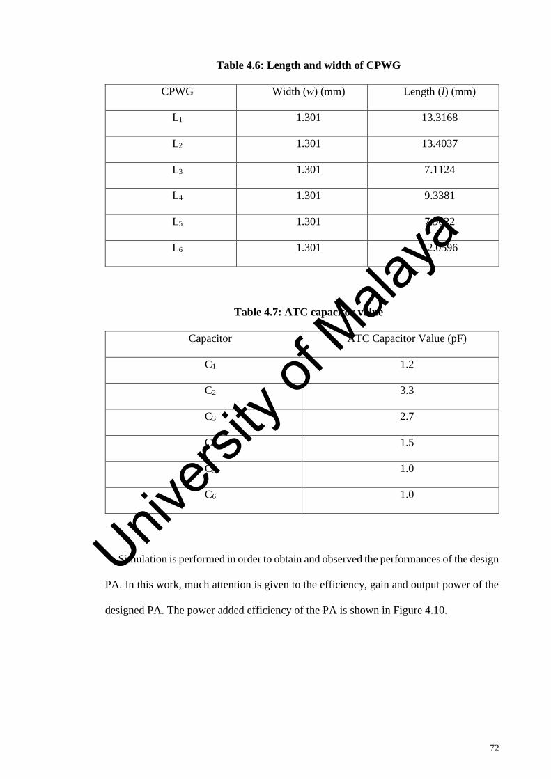
72
Table 4.6: Length and width of CPWG
CPWG Width (w) (mm) Length (l) (mm)
L1 1.301 13.3168
L2 1.301 13.4037
L3 1.301 7.1124
L4 1.301 9.3381
L5 1.301 7.9622
L6 1.301 12.0596
Table 4.7: ATC capacitor value
Capacitor ATC Capacitor Value (pF)
C1 1.2
C2 3.3
C3 2.7
C4 1.5
C5 1.0
C6 1.0
Simulation is performed in order to obtain and observed the performances of the design
PA. In this work, much attention is given to the efficiency, gain and output power of the
designed PA. The power added efficiency of the PA is shown in Figure 4.10.
Univers
ity of
Mala
ya

73
Figure 4.10: Graph of PAE against frequency of GaN PA (Simulation)
From the simulation result, the efficiency of the designed PA achieved a satisfactory
performance. In the desired frequency range from 80 Mhz to 2200 MHz, the PAE of the
designed PA achieved around of 55% to 69%.
The simulation result of gain of the PA is shown in Figure 4.11. The gain obtained
from simulation shows a stable performance across the desired bandwidth, which is
around 14 to 15 dB in the frequency range of 80 MHz to 2200 MHz
0
10
20
30
40
50
60
70
80
0 0.2 0.4 0.6 0.8 1 1.2 1.4 1.6 1.8 2 2.2
PAE
(%)
Frequency (GHz)
Univers
ity of
Mala
ya

74
Figure 4.11: Graph of gain against frequency of GaN PA (Simulation)
For output power, the overall output power achieved by the designed PA is considered
remarkable. The output power achieved by PA is in the range of 39 dBm to 42 dBm. The
simulation result is shown in Figure 4.12.
Figure 4.12: Graph of output power against frequency of GaN PA
0
5
10
15
20
0 0.2 0.4 0.6 0.8 1 1.2 1.4 1.6 1.8 2 2.2
Gai
n (
dB
)
Frequency (GHz)
0
10
20
30
40
50
0 0.2 0.4 0.6 0.8 1 1.2 1.4 1.6 1.8 2 2.2
Ou
tpu
t P
ow
er
(dB
m)
Frequency (GHz)Univers
ity of
Mala
ya

75
In this section, the simulation results of the GaN PA are observed and discussed. In
general, the performances of the designed PA based on simulation are considered
remarkable. The PA is able to achieved maximum PAE of 69%. The output power of the
designed PA is around 41 dBm and the device shows a stable gain of 14 to 15 dB across
the desired frequency range of 80 MHz to 2200 MHz.
Univers
ity of
Mala
ya

76
4.4 Measurement Results
In this section, the measurement results of the designed PA are presented. The
measurement results are analyzed and compered with the simulation results obtain.
Experimental results usually would be deviated with simulation results, as the simulation
results are obtain in the ideal situation. For example in this work, DC biasing circuit in
simulation is in the ideal condition, therefore the results obtain are often better than
expected. Before discussion of measurement results, fabrication of PCB is briefly
presented.
In this section, experiment is carried out in order to obtain measurement results. The
measurement setup is discussed in section 3.8. Measurement results obtained are
compared with simulation results. The spectrum analyzer is set to the measured frequency
with zero span and the marker is placed at the peak of the signal to obtain accurate
displayed output power. The measured efficiency, output power and gain of the designed
PA are presented and compared with simulation results.
The measured PAE of the GaN wideband PA is shown in Figure 4.13. The graph of
measured PAE and simulated PAE are shown in the same graph for comparison purpose.
Univers
ity of
Mala
ya

77
Figure 4.13: Simulated and Measured result of PAE for GaN PA
From the graph, it is observed that the measured PAE of the designed PA is in
agreement with the simulated data in the range of 80 MHz to 1800 MHz, which the PAE
achieved around 54% to 67%. However, the performance of the efficiency degraded after
the frequency of 1800 MHz, which fall towards 40% efficiency. The outcome is still
acceptable for wide bandwidth application.
The measured gain of the designed PA is shown in Figure 4.14. Simulated data and
measured data are presented in a same graph.
0
10
20
30
40
50
60
70
80
0.1 0.2 0.4 0.5 0.8 1 1.3 1.5 1.8 2 2.1 2.2
PAE
(%)
Frequency (GHz)
PAE (Simulated) PAE (Measured)
Univers
ity of
Mala
ya

78
Figure 4.14: Simulated and Measured result of gain for GaN PA
The gain of the GaN PA demonstrated a stable performance across the bandwidth, and
also less deviated from the simulated results. Measured gain achieved 13dB to 18dB in
the range of 80 MHz to 2200 MHz, which is considered as a remarkable achievement.
The performance of the PA declined after 2000 MHz to around 11dB but the overall gain
is acceptable for wideband PA.
The measured output power is shown in Figure 4.15. Both of simulated and measured
data are shown in the graph for comparison purpose.
0
5
10
15
20
25
30
35
40
0.1 0.2 0.4 0.5 0.8 1 1.3 1.5 1.8 2 2.1 2.2
Gai
n (
dB
)
Frequency (GHz)
Gain (Simulated) Gain (Measured)
Univers
ity of
Mala
ya

79
Figure 4.15: Simulated and Measured result of output power for GaN PA
The measured output power of the GaN PA showed a satisfactory achievement. Output
power measured 40 dBm to 42 dBm in the frequency range of 80 MHz to 2200 Mhz,
although at high frequency (2000 Mhz and above) the output power demonstrated a fall
towards 35 dBm. In general the measured data did not show much deviation from
simulated result.
Overall, the PAE, gain and output power of the GaN PA achieved satisfactory
performances with reasonable agreement with simulated data.
05
101520253035404550
0.1 0.2 0.4 0.5 0.8 1 1.3 1.5 1.8 2 2.1 2.2
Ou
tpu
t P
ow
er
(dB
m)
Frequency (GHz)
Pout (Simulated) Pout (Measured)
Univers
ity of
Mala
ya

80
4.5 Comparison of performances with various works
In this section, the performances of recent work in the context of GaN wideband PA
are summarized in Table 4.8. The significant of this work compared to other work is this
work gives good performance from 80 MHz to 2200 MHz for high operating gain.
Table 4.8: Comparison of Performances of Wideband Power Amplifier in
different works
Work Device Bandwidth
(GHz)
Efficiency
(%)
Output
Power
(dBm)
Gain (dB)
(Smith &
Cripps,
2016)
GaN
HEMT
0.5-1.5 44-75 45 10
(A.
Grebennikov,
2016)
GaN
HEMT
1.4-2.7 68 41 9
(Bae & Kim,
2016)
GaN
HEMT
2-6 18-22 41-43 22
(Ma, Zhou,
& Yu, 2015)
GaN
HEMT
2.1-2.6 70.7 40.5 12.5
(Aridas et al.,
2014)
LDMOS 0.27-0.56 65 38.5 10
(Wu,
Mkadem, &
Boumaiza,
2010)
GaN
HEMT
1.9-2.9 63 45.8 10.8
This work GaN
HEMT
0.08-2.2 45-67 34-41 13-18
Univers
ity of
Mala
ya

81
4.6 Summary
In this chapter, the results obtained from experiment are presented and discussed. First,
IMN and OMN are developed from the RFT algorithm and the schematic of each
matching network is presented. The performance of the matching network obtained is
based on the TPG graph.
Next, mixed-lumped design is implemented in both of the matching networks.
Inductors are replaces with CPWG transmission line which contributes to the distributed
elements and high-Q ATC capacitor is selected to represent capacitor on PCB level. The
method of choosing the parameter of CPWG transmission line and method of selection
of ATC capacitor are discussed.
Simulation of matching networks with mixed-lumped design is carried out in order to
validate the designed matching networks with the reference of TPG graph. Then, the
matching networks with mixed-lumped designed connected with GaN transistor and
biasing circuit are simulated to observe the PAE, gain and output power of the PA.
The completed PA PCB is used to carry out experiment in order to obtain measurement
data. The measurement data of PAE, gain and output power are compared with simulation
data. Comparison of performances of wideband PA in various work has been presented.
Univers
ity of
Mala
ya

82
CHAPTER 5: CONCLUSION
5.1 Conclusion
In this work, a wideband PA for GaN HEMT is designed for tow-way radio
application. The methodology of the PA designed is discussed from the development of
matching networks towards the fabrication of prototype for measurement purpose. A
technique called RFT is employed in the process of matching networks development.
Mixed-lumped elements design is implemented in the matching networks, in specific the
inductor in represented by CPWG transmission line and high-Q ATC 100A series
capacitor is selected to represent lumped element. For measurement data, the proposed
PA design with GaN HEMT presents a satisfactory achievement in terms of PAE, output
power and gain in the frequency range of 80 MHz to 2200 MHz, and have reasonable
agreement with simulated data. The maximum PAE of the PA achieved 69% (range of
39% to 69%) and the gain is more than 13 dB which considered good gain achievement.
The output power of the PA achieved 40 dBm to 43 dBm in the frequency range. The PA
designed for wideband operation across low frequency (80 MHz) to higher frequency
(2200 MHz) achieved state-of-the-art performances. Hence, the proposed methodology
in this paper is practical with simplest circuit configuration and enhanced performances,
which fulfills the objectives of this research work.
5.2 Future Work
This research work has develop a wideband PA employing RFT and mixed lumped-
distributed elements implementation. The key point of this designed is to employ the
methodology mentioned to obtained wideband PA with enhanced performances and in
simplest circuit form. The measurement results of the designed PA are presented in
Chapter 4. As we can observed the although the measurement performances of designed
PA is in good agreement with the simulation data, the results at the higher frequency end
(after 2 GHz) showed degradation due to loss, limitation of equipment and errors on the
Univers
ity of
Mala
ya

83
circuit construction. This design can be further improved by adding figure-of-merits such
as 3db back-off region, linearity, 1db compression point in order investigate in depth of
the PA designed. Also, this designed can be extended to high frequency application (up
to 20 Ghz), such as millimeter wave application which is an important application in
future 5G communications.
Univers
ity of
Mala
ya

84
REFERENCES
Aridas, N. K., Yarman, B. S., & Chacko, P. (2014). Wideband power amplifier for two-
way radio applications via real-frequency technique. Electronics letters, 50(23),
1762-1764. doi:10.1049/el.2014.2972
Bae, K. T., & Kim, D. W. (2016). 2–6 GHz GaN distributed power amplifier MMIC with
tapered gate‐series/drain‐shunt capacitors. International Journal of RF and
Microwave Computer‐Aided Engineering, 26(5), 456-465.
Bowick, C., Blyler, J., & Ajluni, C. (2008). Chapter 5 - The Transistor at Radio
Frequencies RF Circuit Design (Second Edition) (pp. 103-123). Burlington:
Newnes.
Carlin, H., & Civalleri, P. (1998). Electronic engineering systems series. Wideband
Circuit Design.
Carlin, H. J. (1977). A new approach to gain-bandwidth problems. Circuits and Systems,
IEEE Transactions on, 24(4), 170-175.
Carlin, H. J., & Civalleri, P. P. (1985). On flat gain with frequency-dependent
terminations. Circuits and Systems, IEEE Transactions on, 32(8), 827-839.
Chen, P., Xia, J., Merrick, B. M., & Brazil, T. J. (2017). Multiobjective Bayesian
Optimization for Active Load Modulation in a Broadband 20-W GaN Doherty
Power Amplifier Design. IEEE Transactions on Microwave Theory and
Techniques, 65(3), 860-871. doi:10.1109/TMTT.2016.2636146
El Din, M. G., Geck, B., & Eul, H. (2009). Adaptive matching for efficiency enhancement
of GAN class-F power amplifiers. Paper presented at the Wireless Sensing, Local
Positioning, and RFID, 2009. IMWS 2009. IEEE MTT-S International
Microwave Workshop on.
Fano, R. M. (1950). Theoretical limitations on the broadband matching of arbitrary
impedances. Journal of the Franklin Institute, 249(1), 57-83.
Grebennikov, A. (2005). RF and microwave power amplifier design: McGraw-Hill New-
York.
Grebennikov, A. (2016). High-Efficiency Class-E Power Amplifier With Shunt
Capacitance and Shunt Filter. IEEE Transactions on Circuits and Systems I:
Regular Papers, 63(1), 12-22. doi:10.1109/TCSI.2015.2512698
Grebennikov, A., Sokal, N. O., & Franco, M. J. (2012). Switchmode RF and microwave
power amplifiers: Academic Press.
Kılınç, S., Köprü, R., Aksen, A., & Yarman, B. S. (2014, 12-14 Dec. 2014). Mixed
element wideband microwave amplifier design via simplified real frequency
technique. Paper presented at the Proceedings of 2014 Mediterranean Microwave
Symposium (MMS2014).
Univers
ity of
Mala
ya

85
Krishnamurthy, K., Vetury, R., Keller, S., Mishra, U., Rodwell, M. J., & Long, S. I.
(2000). Broadband GaAs MESFET and GaN HEMT resistive feedback power
amplifiers. IEEE Journal of Solid-State Circuits, 35(9), 1285-1292.
Kuh, E., & Patterson, J. (1961). Design theory of optimum negative-resistance amplifiers.
Proceedings of the IRE, 49(6), 1043-1050.
Kumar, N., & Grebennikov, A. (2015). Distributed Power Amplifiers for RF and
Microwave Communications: Artech House Publishers.
Kumar, N., Prakash, C., Grebennikov, A., & Mediano, A. (2008). High-efficiency
broadband parallel-circuit class E RF power amplifier with reactance-
compensation technique. IEEE Transactions on Microwave Theory and
Techniques, 56(3), 604-612.
Lindberg, P., Sengul, M., Cimen, E., Yarman, B., Rydberg, A., & Aksen, A. (2006). A
single matching network design for a dual band PIFA antenna via simplified real
frequency technique. Paper presented at the Proc. 1st European Conference on
Antennas and Propagation.
Ma, L., Zhou, J., & Yu, Z. (2015, 6-9 Dec. 2015). Design of a high-efficiency dual-band
harmonic-tuned power amplifier via simplified real frequency technique. Paper
presented at the 2015 Asia-Pacific Microwave Conference (APMC).
Mohadeskasaei, S. A., & Zhou, X. (2016, 27-29 July 2016). A 30 watt high efficient high
power RF pulse power amplifier. Paper presented at the 2016 IEEE MTT-S
International Conference on Numerical Electromagnetic and Multiphysics
Modeling and Optimization (NEMO).
Mughal, F. A., Kashif, A., Cheema, N. B., Imran, M., & Azam, S. (2015, 13-17 Jan.
2015). Design and fabrication of a GaN HEMT based amplifier for wideband
applications. Paper presented at the 2015 12th International Bhurban Conference
on Applied Sciences and Technology (IBCAST).
Narendra, K., Limiti, E., Paoloni, C., Collantes, J.-M., Jansen, R., & Yarman, S. (2012).
Vectorially combined distributed power amplifiers for software-defined radio
applications. Microwave Theory and Techniques, IEEE Transactions on, 60(10),
3189-3200.
Rhea, R. (2006). The Yin-Yang of Matching: Part 1—Basic Matching Concepts. High
Frequency Electronics, 5(3), 16-25.
Richards, P. I. (1948). Resistor-Transmission-Line Circuits. Proceedings of the IRE,
36(2), 217-220. doi:10.1109/JRPROC.1948.233274
Sertbas, A., & Yarman, B. S. (2004). A computer-aided design technique for lossless
matching networks with mixed, lumped and distributed elements. AEU-
International Journal of Electronics and Communications, 58(6), 424-428.
Smith, R. M. H., & Cripps, S. C. (2016, 3-4 Oct. 2016). Broadband push-pull power
amplifier design at microwave frequencies. Paper presented at the 2016 11th
European Microwave Integrated Circuits Conference (EuMIC).
Univers
ity of
Mala
ya

86
Wu, D. Y. T., Mkadem, F., & Boumaiza, S. (2010, 23-28 May 2010). Design of a
broadband and highly efficient 45W GaN power amplifier via simplified real
frequency technique. Paper presented at the 2010 IEEE MTT-S International
Microwave Symposium.
Yarman, B. (1982). A SIMPLIFIED REAL FREQUENCY TECHNIQUE FOR BROAD-
BAND MATCHING A COMPLEX GENERATOR TO A COMPLEX LOAD.
RCA review, 43(3), 529-541.
Yarman, B. S. (2008). Design of ultra wideband antenna matching networks: via
simplified real frequency technique: Springer Science & Business Media.
Yarman, B. S. (2010). Design of ultra wideband power transfer networks: John Wiley &
Sons.
Yarman, B. S., & Aksen, A. (1992). An integrated design tool to construct lossless
matching networks with mixed lumped and distributed elements. Circuits and
Systems I: Fundamental Theory and Applications, IEEE Transactions on, 39(9),
713-723.
Yarman, B. S., Aksen, A., & Kilinç, A. (2001). An immitance based tool for modelling
passive one-port devices by means of darlington equivalents. AEU-International
Journal of Electronics and Communications, 55(6), 443-451.
Yarman, B. S., & Carlin, H. J. (1982). A simplified" real frequency" technique applied to
broad-band multistage microwave amplifiers. Microwave Theory and Techniques,
IEEE Transactions on, 30(12), 2216-2222.
Zhang, W., Yamamoto, Y., Oehme, M., Matthies, K., Raju, A. I., Srinivasan, V. S., . . .
Funk, H. (2016). S-parameter characterization and lumped-element modelling of
millimeter-wave single-drift impact-ionization avalanche transit-time diode.
Japanese journal of applied physics, 55(4S), 04EF03.
Univers
ity of
Mala
ya

87
LIST OF PUBLICATIONS AND PAPERS PRESENTED
ISI-Cited Journal papers:
1. Narendra Kumar, Wen Jun Lim, B. S. Yarman, Prakash Chacko, “A Practical
Design Methodology of Wideband UHF RF Power Amplifiers for Two-Way
Radio Applications” in IEEE Transaction on Microwave Theory and Techniques.
(Under Revision with Major Correction)
2. Wen Jun Lim, Narendra Kumar, B. S. Yarman, Prakash Chacko, “Ultra-
wideband GaN HEMT Power Amplifier with Practical Mixed Lumped Approach
Employing Real-Frequency Technique” in IEICE Electronic Express. (Published
on 10/7/2017)
Conference:
1. Wen Jun Lim, Narendra Kumar, “Design of Wideband Power Amplifier for GaN
HEMT for Two-Way Radio Application.” 2016 IEEE Industrial Electronics and
Applications Conference, Kota Kinabalu, Sabah, Malaysia, 20-22 November
2016.
Univers
ity of
Mala
ya