University of Naples Federico II - unina.it · University of Naples Federico II ... Drugs can be...
72
University of Naples Federico II International PhD program on NOVEL TECHNOLOGIES FOR MATERIALS, SENSORS AND IMAGING XXVIII cycle PhD School in Industrial Engineering PhD Thesis Fabrication of microdevices for biomedical applications based on lithographic approach Alessandro Caliò Supervisor: Dr. Luca De Stefano Institute for Microelectronics and Microsystems National Council of Research
Transcript of University of Naples Federico II - unina.it · University of Naples Federico II ... Drugs can be...

University of Naples Federico II
International PhD program on NOVEL TECHNOLOGIES FOR MATERIALS, SENSORS AND IMAGING
XXVIII cycle
PhD School in Industrial Engineering
PhD Thesis
Fabrication of microdevices for biomedical
applications based on lithographic approach
Alessandro Caliò
Supervisor: Dr. Luca De Stefano
Institute for Microelectronics and Microsystems
National Council of Research

2

3
A mio nipote Tommaso e alle mie nipoti Alice, Nicole e Rebecca.

4

Table of contents
5
Table of contents
1. Introduction pag. 7
2. Materials and Methods pag. 16
2.1. Materials pag. 16
2.1.1. Hydrogels pag. 17
2.1.2. SU-8 photoresist pag. 18
2.1.3. Polydimethylsiloxane pag. 19
2.1.4. Norland optical adhesive pag. 20
2.1.5. Porous silicon pag. 20
2.2. Microfabrication processes pag. 21
2.2.1. Photolithography pag. 22
2.2.2. Soft imprint lithography pag. 23
2.3. Microneedles fabrication pag. 24
2.4. Microneedles based hybrid device fabrication pag. 25
2.5. Microneedles based enzymatic electrodes fabrication pag. 27
2.6. Filter based microfluidic device fabrication pag. 29
3. Microneedles pag. 31
3.1. Height, base and curvature radius characteristics pag. 31
3.2. Indentation hardness and skin penetration properties pag. 34
4. Transdermal delivery of small molecules by microneedles based
hybrid patch pag. 37
4.1. Microneedles based hybrid patch pag. 38
4.2. Optically monitored administration of fluorescein molecules pag. 38
5. Transdermal biosensing of biological molecules by microneedles
based enzymatic electrodes pag. 44
5.1. Microneedles based enzymatic electrodes pag. 44
5.2. Electrochemical detection of glucose and lactic acid molecules pag. 45
6. Filtration of small molecules by filter based microfluidic device pag. 50
6.1. Plastic photomask pag. 51
6.2. Filter based microfluidic device pag. 52
6.3. Optically monitored filtration of rhodamine molecules pag. 53
7. Conclusions pag. 56
8. References pag. 60

Table of contents
6
Appendix A - Lists of publications and research experiences in
external labs related to the PhD work pag. 66
Appendix B - List of publications related to other research activities
investigated during the PhD program pag. 68
1. Introduction
7
1. Introduction
Health care and devices used to delivery and monitor health are unquestionably among the
most important and critical elements in our society today, and they will continue to become
even more important in the future as the world population grows, and the demand for
improved quality and more diverse distribution of health services delivered increases. During
the past few decades, significant improvements were done in understanding the origin of
various diseases, in development of new and exciting tools to fight and detect diseases, and
obviously in cost of delivering health care. Prevention and treatment are equally important as
our society moves into the twenty first century, and these show an ever increasing need for
better equipment and facilities to assist in delivering the highest quality health care. These
equipments need to provide the highest performance at the lowest possible cost. In spite of
significant progresses made in both of these areas, today there are serious limitations imposed
on our health care delivery due to very high costs involved. Any new technology that can help
reduce this cost will undoubtedly find a significant market and will lay the foundation for the
development of a new generation of biomedical systems. A possible roadmap leads to the
realization of biomedical devices and systems using microfabrication processes, traditionally
used for manufacture integrated circuits.
Microfabrication processes have revolutionized pharmaceutical, medical and biological fields
since they offer the possibility for highly reproducible mass fabrication of systems with
complex geometries and functionalities, including novel drug delivery systems and
bionsensors (Betancourt et al., 2006). Microdevices, realized using microfabrication
processes, have many advantages over their macroscale counterparts. For instance,
miniaturization allows manufacturing of portable, hand-held, implantable or even injectable
microdevices. In addition, as a result of their minute size, these microdevices need less
sample or reagent for analysis or operation, saving money and time. Moreover, where
materials and/or processes are inhibited by lengthy diffusion times, miniaturization provides a
mechanism for shortening these ones. A notable example where these microdevices allow for
significant advantages over traditional counterparts is in medical care: point of care diagnostic
testing, which is testing performed at the patient’s bedside, permits physicians to diagnose a
patient’s conditions more rapidly than conventional lab based testing. By using these
microdevices to reduce the time of diagnoses, the physician is able to make better patient
management decisions leading to improved patient outcomes and reduce the overall cost of
care. The basic microfabrication process is based on deposition, patterning, doping and

1. Introduction
8
etching steps (Sze, 2008). Deposition consists in placing a thin layer (or film), such as an
insulating silicon dioxide layer, on a substrate, such as a silicon wafer, using chemical or
physical process. A light-sensitive resist, called photoresist, is then deposited on the top of the
thin layer and patterned using photolithography (or optical lithography). Finally, the pattern is
transferred from the photoresist layer to the thin layer by dry or wet etching process. After
removing the remaining photoresist, a next layer can be deposited and structured, and so on.
Doping of a semiconductor material, such as silicon, by ion implantation or diffusion process
can be done directly after photolithography. Traditionally, silicon, glass and ceramics are used
as substrates, dielectric, metal and polycrystalline silicon are used as thin layers and some
particular commercial polymers, such as SU-8, are used as photoresists. These materials are
commonly called hard materials and show superior mechanical properties which make them
suitable for the realization of a large variety of microdevices (microprocessors,
accelerometers, and so on). Microfabrication processes, and related materials, were developed
for applications in the semiconductor industry and are, consequently, not specific for
biological, medical and other applications. In some fields, such as biological and biomedical,
the use of the hard materials is not the more suitable choice (Quake et al., 2000). For example,
many biomedical applications require delicate surface chemistry that is difficult to achieve
with high temperatures required to bond silicon and glass. The so called soft materials, mostly
based on polymers, such as hydrogel, polydimethylsiloxane (PDMS), norland optical
adhesive (NOA), can be used to overcome many of the limitations of the hard materials.
Polymers are inexpensive, biocompatible therefore provide a more suitable interface with
biological tissue, reducing irritation and scarring, and can be used in disposable devices. A
specific group of fabrication processes, called soft lithography, was developed to realize
microdevices using soft materials (Gates et al., 2005; Lipomi et al., 2012). Some of them are
microcontact printing, microtransfer molding and replica molding. The combination of hard
materials and processes with soft ones allows to benefit from the advantages of both,
providing the realization of microdevices with functionalities that are difficult to achieve with
only hard materials and processes or only soft ones. Microfabricated devices, like
microelectromechanical systems (MEMS), lab-on-a-chip (LoC) and micro-total analysis
systems (micro-TAS), have been designed for more than thirty years, but only in the last few
years they are gaining great success. High throughput, small sample volumes, high surface-
area-to-volume ratio, commercially scale-up and so on demands in several fields, like biology
and chemistry, have created a need for these devices. Interest in using MEMS for in vivo
applications is started in the 1990s in the academic world. Biomedical
1. Introduction
9
microelectromechanical systems (BioMEMS) are now a heavily researched area with a wide
variety of important biomedical applications. In general, BioMEMS can be defined as devices
or systems, constructed using techniques inspired from micro/nano-scale fabrication, used for
processing, delivery, manipulation, analysis, or construction of biological and chemical
entities. Most of the activities in the BioMEMS area are moving towards commercialization
of these biomedical devices and systems (Ziaie et al., 2004). For example, a MEMS based
DNA sequencer developed by the Cepheid is currently being installed in post offices across
USA for bioagent detection. BioMEMS drug delivery systems are also actively targeted by
many investigators and companies as is evident, for example, from current efforts by
MicroCHIPS, to commercialize an electronically activated drug delivery microchip, by
ChipRx, to introduce systems that integrate silicon and electroactive polymer technologies for
controlled delivery, and by iMEDD, to develop nanoporous membranes and micromachined
particles for a variety of drug delivery applications. Large efforts are dedicated to realize
others commercial BioMEMS, such as microneedles based devices for transdermal drug
delivery and transdermal biosensing, and microfluidic device for microdialysis.
The aim of the scientific research investigated in these three years of PhD course is to define
the fabrication procedures, based on lithographic processes on both hard and soft materials,
for the realization of innovative microdevices for biomedical applications. In particular,
microneedles based devices for drug delivery and biosensing, and device for microfluidic
filtration have been explored.
Microneedles are three-dimensional structures and represent the interface between a device
and the patient’s body for extracting, sampling or releasing physiological fluid. The length of
microneedles should be long enough that they can penetrate epidermis and short enough not
to reach dermis, in order to avoid any pain. The concept of microneedles was proposed in the
1970s, but it was not realized experimentally until the 1990s when the industry of
microelectronics provided the microfabrication tools essential to make such small structures.
Microfabrication processes are the most promising to fabricate optimal microneedles for any
application. The first microneedle arrays reported in literature were developed by etching the
silicon wafer for intracellular delivery (Campbell et al., 1991). These needles were inserted
into cells and nematodes to increase molecular uptake and gene transfection. After that, a
number of attempts were made by various researchers to develop different designs. Several
categories of microneedles were reported in literature for various applications. Microneedles
can be categorized on the basis of the shape (cylindrical, conical, pyramidal, etc) (Ashraf et
al., 2010) and feature (solid, hollow, dissolving, etc) (Chandrasekaran, 2003; Sachdeva et al.,

1. Introduction
10
2011). Microneedles can also be classified on the basis of materials (Ashraf et al., 2010),
depending on application. Most of researchers used silicon for microneedles fabrication
(Wilke et al., 2005; Ashraf et al., 2010), since it is inexpensive, of high purity and there are a
lot of fabrication procedures, coming from the microelectronics industry, able to manipulate
this material. However, silicon is a brittle material and can be harmful to health. Different
researchers have understood this critical issue and shifted to soft materials. Fabrication of
microneedles were reported using various soft materials such as polyglycolic acid (PGA),
poly(methyl methacrylate) (PMMA), PDMS, and so on (Aoyagi et al., 2008; Kochhar et al.,
2013). Typical lengths of microneedles are in the range of 100-300 µm for drug delivery
(Ashraf et al., 2010; Chen et al., 2010), 1100-1600 µm for blood extraction (Tsuchiya et al.,
2005). Various fabrication techniques/processes were developed and used for microneedles
fabrication such as hot embossing (Oh et al., 2008), laser micromachining (Bhandari et al.,
2008), micromolding (Lee et al., 2008), coherent porous silicon etching (Rajaraman et al.,
2005), photolithography (Shibata et al., 2007). Currently, the most important application areas
of microneedles can be considered transdermal drug delivery and transdermal biosensing.
Development of functional delivery systems for active pharmaceutical ingredients is a
challenging task. Drugs can be administered through most common routes like oral, parenteral
and transdermal route, as well as less explored routes such as nasal, pulmonary and buccal
(Langer, 2001). Each of these routes has specific pros and cons. Oral drug delivery systems
offer advantages such as patient compliance, large surface area with rich blood supply for
absorption, low cost, easiness in engineering of drug release in stomach/intestine. However,
limitations, such as drug degradation in gastrointestinal tract, first pass metabolism, poor
absorption, local irritation and variability in absorption (due to factors like pH, motility, food,
mucus layer), are associated with these drug delivery systems. The parenteral route offers
advantages like quick onset of action, accurate drug delivery and continuous drug delivery by
infusion. Its major limitations include pain associated with the injections, expertise required to
drug deliver, risk of infection and difficulty in obtaining sustained drug delivery. Transdermal
drug delivery involves the transport of drug across the skin. Optimal physiochemical
properties are required in drug candidates for delivery via transdermal patches. Transdermal
drug delivery offers advantages like patient compliance, avoidance of first pass metabolism,
large surface area of skin over which to deliver the drug, quick termination of dosing.
However, only a few products with optimum characteristics were successfully marketed to
deliver a drug through the skin. Skin can be divided into three regions: 1) the outer most
cellular layer, called epidermis, which contains the stratum corneum; 2) the middle layer,

1. Introduction
11
called dermis; 3) the inner most layer, called hypodermis. Skin varies in thickness, according
to anatomic site and age of individual. The epidermis layer, whose thickness varies between
50 and 150 µm, is made up of viable cells without a vascular network. This layer obtains its
nutritional needs by passive diffusion through interstitial fluid. The outermost layer of the
epidermis, that is the stratum corneum (20-40 µm), consists of dead cells, which act as a hard
barrier. The dermis, an integrated fibro-elastic structure that has a thickness of about 500-
2000 µm, provides mechanical strength to the skin. This layer contains an extensive nervous
and vascular network. The pain associated with parenteral drug delivery is due to possible
damage to the nerves endings within the dermis. For drug delivery across the skin, the
challenge is to cross the intact stratum corneum layer without causing damage to nerves
endings. Only a few potent drug molecules, with high lipophilicity and small molecular
weight (< 500 Da), can be administered directly through passive diffusion (Matteucci et al.,
2008). Various chemical and physical approaches were employed to improve drug penetration
across the skin (Milewski et al., 2010). Chemical approaches include use of penetration
enhancers, like surfactants, fatty acids/esters and solvents to dissolve the stratum corneum
lipid or to increase the solubility of drugs. Physical approaches, like electroporation,
ionphoresis, magnetophoresis and sonophoresis, were found suitable to create pathways for
only few drugs across the skin. The aforementioned approaches are associated with certain
drawbacks: chemical approaches are often associated with higher skin irritation and are
applicable only to small molecules, while physical methods typically require a device with a
power supply which adds to the cost and complexity. Searching for inexpensive and reliable
way to administer the drug safely to the epidermal layer without damaging the nerve cells of
dermis, and minimizing chances of microbial penetration, led to the development of
microneedles (Donnelly et al., 2009).
Integration of biorecognition and signal transduction elements is an important area of
biosensors research. Analytical devices combining the specificity of biological systems with
the advantages of electrochemical transduction have gained an increased popularity in the last
two decades. Enzymatic redox reactions are particularly amenable to be interfaced with
electrochemical transducers, since electron exchange is a key step in their natural cycle. In
general, enzymes can operate in liquid environments or immobilized on various supports.
Immobilized means that the enzyme is unable to move, but the enzyme activity still remains
in the analytical device, although in a generally minor extension when compared with free
enzymes. The main advantages of enzymes immobilized on supports compared to free
enzymes systems are reduction of costs of operations, higher enzyme stability, ability to stop

1. Introduction
12
the reaction rapidly by simply removing the enzyme from the reaction solution, the fact that
products are not contaminated with the enzyme and the possibility of establishing a model
system to study enzyme action with variable applications. Enzyme based electrodes are an
important class of biosensors where by products of enzymatic breakdown of an analyte are
electrochemically detected. Enzyme immobilization on the electrode with maintained enzyme
activity is a challenging task. The choice of immobilization method depends on many factors,
such as the nature of the biological element, the type of transducer used, the physicochemical
properties of the analyte and the operating conditions in which the biosensor should work, and
overriding all these considerations is necessary for the biological element to exhibit maximum
activity in its immobilized microenvironment. Generally, there are four regular methods for
enzyme immobilization: adsorption, covalent bonding, crosslinking and entrapment (Nunes et
al., 2006). The entrapment method is the most adapt for the realization of enzyme-based
electrodes. This method refers to a mixture of biomaterial and monomer solution that
polymerizes to a gel, trapping the biological component. Hydrogels are attractive materials in
fabricating enzyme-based electrodes by entrapment method, since a hydrated gel provides an
excellent matrix for encapsulation of functional enzymes (Pishko et al., 1991) that maintains
intact the enzyme activity. Microneedles made by hydrogels are particularly attractive for
making enzyme based electrodes for transdermal biosensing, because offers remarkable
opportunities for moving microdevices from research laboratories to real field applications,
and easy envisage to use point of care microdevices with pain free, minimally invasive, low
cost and minimal training features, that are very attractive for both developed and emerging
countries. Microneedles allow the realization of a new class of transdermal biosensors for
electrochemical measurement of analytes of clinical interest, such as biomarkers, glucose,
lactic acid, upon insertion of the needles in superficial layer of the skin. Diabetes is one of the
leading causes of death and disability in the world. There is a large population suffering from
this disease and the healthcare costs increase every year. It is a chronic disorder resulting from
insulin deficiency and hyperglycemia and has a high risk of complications development for
eyes, kidneys, peripheral nerves, heart and blood vessels. The lactic acid, or more commonly
its negative ion called lactate, plays an important role in (sports) medicine, in the nutritional
sector and touches environmental concerns. Determination of lactic acid concentration in
blood is essential for the diagnosis of patient conditions in intensive care and during surgery.
An elevated lactic acid level in blood is a major indicator of ischemic conditions of the
respective tissue. This ischemic situation can be caused by all types of shock, suffocation and
respiratory insufficiency, carbon monoxide or cyanide intoxication, heart failure, and so on.

1. Introduction
13
Another reason for an altered lactic acid level is a disturbed lactic acid metabolism, which
may be caused by diabetes or absorptive abnormalities of short chain fatty acids in the colon.
In other fields of medicine, lactic acid plays an important role as well. In sports medicine
(training of athletes or racing animals) or space medicine, blood lactic acid levels during
exercise are indicators for training status and fitness. Quick diagnosis and early prevention are
critical for the control of the disease status related to these two analytes. Most of devices that
quantify glucose level operate by measuring it in blood sample that is generally taken from
the fingertip since this procedure provides the most accurate result, but it also causes the
patient pain because of fingertips contain many nerve endings. Moreover, the inability of
current devices to continuously monitor the glucose level causes the need to do repetitive
measurements each day resulting in protracted discomforts. Among the various conventional
analytical methods available for the determination of lactic acid, colorimetric tests and
chromatographic analysis are the most important. However, the major part of these methods is
complex, laborious and slow, complicated by intensive sample pretreatment and reagent
preparation. Therefore, the development of alternatives for glucose and lactic acid detection,
with features of pain free, minimal invasion, biocompatibility, on one side, and simplicity,
fast, low cost, real time with no need of sample preparation, on the other side, is very
interesting and, above all, highly required from the dimensions of the market and huge
demand.
Microfluidics is a multidisciplinary field of investigation, involving almost all the scientific
branches of knowledge, such as physics, biology, engineering, chemistry and
microtechnology. Conceptually, the idea under microfluidics is that fluids can be precisely
manipulated using a microdevice built with technologies developed by semiconductor
industry. Microfluidics can be defined as the science that studies the manipulation of small
(10-9
to 10-18
litres) amounts of fluids, using channels with dimensions of tenths to hundreds
micrometres. Microfluidic devices, commonly referred to as micro-TAS and LoC, have many
advantages as they can decrease sample and reagent consumption and increase automation,
thus minimizing the analysis time. Microfluidic devices exploit their most obvious
characteristic, i.e. the small size, and less obvious characteristics of fluids in microchannels,
such as laminar flow. The small dimension of devices allow for portability, so that biological
and chemical samples can be tested on remote sites where there could not be access to
traditional instrumentation. Microfluidic devices are nowadays employed in chemistry,
biology, neuroscience, bioanalysis, biomechanics and other areas of biology and biomedical
fields (Davis, 2008; Mehta et al., 2009). In the last ten years, the integration of mass transport

1. Introduction
14
control into microfluidic devices by means of particular components, called membranes or
more commonly filters, has showed a growing interest (De Jong et al., 2006). Filter science
and technology is a broad and highly interdisciplinary field, where process engineering,
material science and chemistry meet. Although the use of filters in microfluidics is spreading
across many fields, most applications are found in analytical chemistry. Since analytical
equipment is often sensitive to sample composition, in most cases samples cannot be directly
analyzed and need a pretreatment. This may include selective removal of large components,
impurities and dust on one side and low molecular weight components such as salts on the
other. Furthermore, in many cases the concentration of the components of interest is below
the detection limit of the analysis equipment. In such cases, removal of solvent is necessary.
Filters can manage all these operations. Close to analytical applications, also new fields
emerge in which filters are used, such as cell based studies, microreaction technology and fuel
cells. Many different approaches were reported to realize microfluidic filters. A rough
division into four fabrication methods can be made: direct incorporation of (commercial)
filters, filter preparation as part of the device fabrication process, in situ preparation of filters
and use of filter properties of bulk device material (De Jong et al., 2006). Currently, one of
the most used is in situ preparation of the filter that starts with a microfluidic device and
fabricates the filter inside it by polymerization of a photocurable hydrogel using UV light.
The in situ photopolymerization allows creating the filter in any location of the microfluidic
circuit without the need of a constriction region or other mechanisms that are commonly used
to hold the beads. An additional benefit of this method is its application in existing chip
formats, provided that the used chip material is transparent to UV light.
After this initial introduction, the PhD thesis is composed by other five chapters, from the
second to the sixth: 1) materials and methods; 2) microneedles; 3) transdermal delivery of
small molecules by microneedles based hybrid patch; 4) transdermal biosensing of biological
molecules by microneedles based enzymatic electrodes; 5) filtration of small molecules by
filter based microfluidic device.
The second chapter starts with a brief description of materials, hydrogels, SU-8 photoresist,
PDMS, NOA and porous silicon, and fabrication processes, photolithography and soft imprint
lithography, used. The description of the fabrication process, based on photographic reduction
technique, of homemade plastic photomasks for fast prototyping of microfluidic devices is
also reported. The chapter continues with the realization of microneedles based devices, such
as hybrid device and enzymatic electrodes, and filter based microfluidic device using
materials and fabrication processes previously described.

1. Introduction
15
The third chapter is dedicated to the characterization of microneedles. In the first part,
microneedles are characterized in terms of height and base, and curvature radius of the tips. In
the second part, the indentation hardness, quantified by a penetration test, is characterized in
order to verify the ability of microneedles to penetrate into skin.
A brief description of transdermal drug delivery by conventional approaches and the
overcoming of their limits by using microneedles, topic already widely treated in this
introduction, is summarized in the fourth chapter. The hybrid device based on microneedles,
realized as described in the second chapter, is used for transdermal drug delivery. As proof-
of-concept, the device is used for the releasing of fluorescein molecules, comparable to a
small drug, into a buffer solution, that mimics the human interstitial fluid.
The fifth chapter treats briefly the novel trend on exploiting microneedles for transdermal
biosensing of analytes of clinical interest, already widely described in this introduction.
Microneedles based enzymatic electrodes, realized as described in the second chapter, for
detection of glucose and lactic acid molecules are illustrated.
The sixth chapter summarizes the microfluidic filtration, a topic of relevant interest in many
scientific fields, already widely discussed in this introduction. A small section is dedicated to
the characterization of the homemade plastic photomask, realized as described in the second
chapter. Microfluidic filter fabricated inside the microfluidic device for the filtration of small
rhodamine molecules, realized as described in the second chapter, is characterized.
The thesis ends with conclusions, and some future perspectives.

2. Materials and Methods
16
2. Materials and Methods
Microfabrication, i.e. the generation of structures with dimensions in the range between tens
of nanometers to millimeters, is essential in technology and modern science. It supports
information technology and permeates society through its role in microelectronics,
optoelectronics and so on. Microfabrication has its foundations in microelectronics and it will
continue to be the basis for microprocessors, MEMS, flexible electronic devices, biomedical
systems in the foreseeable future. Photolithography is the most successful process in
microfabrication. It is used to pattern parts of a thin film using the UV light. Essentially,
almost all devices with dimensions in the range between 100 nm to millimeters are
manufactured by this process. Microfabrication is also shifting towards areas outside
microelectronics, such as biotechnology and biochemistry (Bhansali et al., 2012). Materials
science gives great support to development of innovative application of microfabrication:
traditional materials are defined as hard materials, since the most used one is the
semiconductor silicon, but in some of these fields, there is the need to use a set of materials,
the so-called soft materials, much more larger than the classic one, which comprises
polymers, hydrogels and also biological matter. A high number of new microfabrication
processes, the soft lithography processes, has been demonstrated for fabricating high quality
structures with sizes ranging from 30 nm to hundreds of micrometers (Rogers et al., 2005;
Qin et al., 2010). One of the most famous processes is the soft imprint lithography that
consists in transferring a pattern from a soft structure to an imprint material.
This chapter is divided in two parts: the first part is dedicated to the description of
microfabrication processes, photolithography and soft imprint lithography, together with soft
and hard materials used, in particular hydrogels, SU-8 photoresist, PDMS, NOA and porous
silicon; in the second part, these microfabrication processes and materials are illustrated in
practical realization of some devices, such as hybrid device and enzymatic electrodes based
on microneedles, and microfluidic device based on filter.
2.1. Materials
Materials traditionally used in microfabrication are silicon, and silicon related materials such
as silicon nitrides and oxides, porous silicon, amorphous silicon and so on, but also metals
(gold, aluminum, platinum, nickel, chromium), glasses of many different kind. In
photolithography, some particular light sensitive commercial polymers, note as photoresists,
are commonly exploited. Most of them are expensive and primarily limit the use in some
applications, like in vivo application, due to the bio-incompatibility. In order to overcome

2. Materials and Methods
17
these limitations, there is the need of alternative materials, such as soft materials. In the
following, hard and soft materials are described in details.
2.1.1. Hydrogels
Hydrogels are polymeric networks able to swell and/or retain aqueous solutions. Hydrogels
are attractive materials in fabrication of biodevices, since a hydrated gel provides an excellent
matrix for encapsulation of functional biological molecules, such as enzymes and peptides.
Main advantages of hydrogels are briefly summarized in the following: 1) micropatterning by
photolithography; 2) development of biocompatible tissue/sensor interface; 3) near-
physiological conditions that minimize protein denaturation helping them to carry out their
full biological functions; 4) three-dimensional geometry enables them to contain large
quantity of sensing reagent, thereby increasing their signal-to-noise ratio and sensitivity.
Hydrogels are divides in two types: natural, like alginates, chitosan and synthetic, as
poly(ethylene glycol) diacrylate (or PEGDA), polyacrylamide and so on. One of the most
widely used is the PEGDA, available commercially from Sigma Aldrich. PEGDA is a
hydrophilic and biocompatible hydrogel that has been suggested for use in a variety of
biomedical applications (Oh, 2009). PEGDA is poorly immunogenic, non-toxic, is readily
cleared by the kidneys and is approved by the Food and Drug Administration for internal
consumption. Moreover, it is an elastic material. PEGDA is commercially available over a
wide range of molecular weights (Mn) from low, that means polymer with tight mesh, to high
values, that means polymer with wide mesh. PEGDA with high Mn is useful in applications
that require an hard material, such as the realization of microneedles for skin penetration,
instead PEGDA with low Mn is adapt in those cases that need of a robust material but not so
hard, like a microfluidic filter for the separation of biological samples. The key chemical
constituent of the PEGDA is showed in Figure 2.1.
Figure 2.1 Chemical composition of the PEGDA with molecular weight Mn.
The terminal acrylates groups, in presence of a photoinitiator and exposed to UV light, allow
the hydrogel to be crosslinked at room temperature, in order to form an insoluble hydrogel
network. Photoinitiators most frequently used are 2-hydroxy-2-methyl-1-phenyl-propan-1-one

2. Materials and Methods
18
or known as darocur 1173 (see Figure 2.2 (A)) and 2-hydroxy-2-methylpropiophenone (see
Figure 2.2 (B)), available commercially from BASF and Sigma Aldrich, respectively.
Figure 2.2 Chemical composition of 2-hydroxy-2-methyl-1-phenyl-propan-1-one (A) and 2-hydroxy-2-
methylpropiophenone (B).
2.1.2. SU-8 photoresist
SU-8 (see Figure 2.3) is an epoxy based high contrast photoresist, designed for
micromachining and other microelectronic applications, where a thick, chemically and
thermally stable image is desired.
Figure 2.3 Chemical composition of the main constituent in SU-8 photoepoxy: eight oligomers are available for
a high degree of crosslinking upon photoexposure.
SU-8 is available commercially from MicroChem in different viscosities, thus enabling a
wide range of thicknesses (0.5 to 650 μm with a single coat process) that can be obtained
(MicroChem). SU-8 photoresist has excellent imaging characteristics and is able of producing
very high aspect ratio structures. SU-8 is a negative photoresist, therefore is best suited for
applications where it is casted, cured and left permanently on the device, like in the
fabrication of a microfluidic device.
(A) (B)
2. Materials and Methods
19
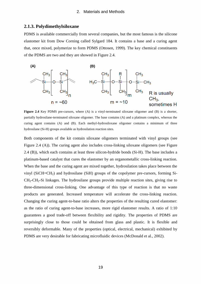
2.1.3. Polydimethylsiloxane
PDMS is available commercially from several companies, but the most famous is the silicone
elastomer kit from Dow Corning called Sylgard 184. It contains a base and a curing agent
that, once mixed, polymerize to form PDMS (Ottosen, 1999). The key chemical constituents
of the PDMS are two and they are showed in Figure 2.4.
Figure 2.4 Key PDMS pre-cursors, where (A) is a vinyl-terminated siloxane oligomer and (B) is a shorter,
partially hydrosilane-terminated siloxane oligomer. The base contains (A) and a platinum complex, whereas the
curing agent contains (A) and (B). Each methyl-hydrosiloxane oligomer contains a minimum of three
hydrosilane (Si-H) groups available as hydrosilation reaction sites.
Both components of the kit contain siloxane oligomers terminated with vinyl groups (see
Figure 2.4 (A)). The curing agent also includes cross-linking siloxane oligomers (see Figure
2.4 (B)), which each contains at least three silicon-hydride bonds (Si-H). The base includes a
platinum-based catalyst that cures the elastomer by an organometallic cross-linking reaction.
When the base and the curing agent are mixed together, hydrosilation takes place between the
vinyl (SiCH=CH2) and hydrosilane (SiH) groups of the copolymer pre-cursors, forming Si-
CH2-CH2-Si linkages. The hydrosilane groups provide multiple reaction sites, giving rise to
three-dimensional cross-linking. One advantage of this type of reaction is that no waste
products are generated. Increased temperature will accelerate the cross-linking reaction.
Changing the curing agent-to-base ratio alters the properties of the resulting cured elastomer:
as the ratio of curing agent-to-base increases, more rigid elastomer results. A ratio of 1:10
guarantees a good trade-off between flexibility and rigidity. The properties of PDMS are
surprisingly close to those could be obtained from glass and plastic. It is flexible and
reversibly deformable. Many of the properties (optical, electrical, mechanical) exhibited by
PDMS are very desirable for fabricating microfluidic devices (McDonald et al., 2002).
(A) (B)

2. Materials and Methods
20
2.1.4. Norland optical adhesive
NOA is a single component liquid adhesive, available commercially from Norland Products,
that cures in seconds to an hard polymer when exposed to UV light (Norland Products). NOA
is sensitive to the UV light with a wavelength range from 320 to 380 nm, with peak sensitivity
around 365 nm. The outstanding characteristic of this adhesive is its extremely fast cure. To
fully cure the material requires 2 J/cm2 of energy. NOA cures to a hard film, but it will not
become brittle. NOA cures not before the desired time. It is also extremely stable when not
exposed to UV light. It has a small amount of resiliency that provides strain relief from
vibrations or temperature extremes. This toughness insures long term performance of the
adhesive bond. NOA cures from the surface down and longer cures are required for thicker
films to allow UV light to penetrate to the full depth. This adhesion improves with age, with
optimum adhesion reached after room temperature aging for one week. This optimum
adhesion can be accelerated by aging at 50 °C for 12 hours. The cured adhesive can withstand
temperatures from -150 °C to 125 °C. Many of the properties (optical, mechanical, etc)
exhibited by NOA are very desirable for fabricating microfluidic devices.
2.1.5. Porous silicon
Porous silicon can be simply described as a network of air holes in a silicon matrix. In most
cases, the porous silicon structure is formed by electrochemical dissolution of a doped
crystalline silicon wafer in hydrofluoric acid (HF) based solution (Smith et al., 1992). In the
anodic I-V curve of silicon in HF based solution, showed in Figure 2.5, it’s possible to
distinguish three regions, called A, B, C.
Figure 2.5 Regions of pore formation (A), transition between pore formation and silicon electropolishing (B)
and silicon electropolishing (C).
Pore formation takes place in region A. At anodic overpotentials in excess of the current peak,
region C, silicon electropolishes. At intermediate overpotentials, region B, a transition zone

2. Materials and Methods
21
exists where pore formation and electropolishing compete for control over the surface
morphology. The resulting structure within the region B is generally porous in nature, but the
pore diameters increase rapidly as the electropolishing potential is approached. Porous silicon
shows a great variety of morphologies dependent on the doping type and level of the silicon
substrate and the electrochemical etching parameters. Usually for a given substrate and
electrolyte, only one type of pore structure can be obtained. The International Union of Pure
and Applied Chemistry guidelines define ranges of pore sizes that exhibit characteristic
absorption properties: pores characterized by a diameter ≤ 2 nm define microporous silicon;
for sizes in the range 2-50 nm the porous silicon is mesoporous; pores diameters > 50 nm are
typical of macroporous silicon. The porous silicon is an ideal material as optical biosensor
transducer and it allows the label-free detection (Dhanekar et al., 2013). Its principal
advantages are: 1) low-cost material and fabrication process; 2) large specific surface area (~
500 m2/cm
3); 3) rapidly and effectively interaction with chemical species; 4) evident changes
in several physical properties usable for label-free sensing (reflectivity, photoluminescence,
electrical conductivity, optical waveguiding, etc); 5) easy integration in hybrid systems
(MEMS, LoC, etc); 6) compatibility with microelectronic technologies; 7) chemically
modification of its surface possible to enhance selectivity in analyte detection. The label-free
sensing mechanism used is based on the change of the porous silicon refractive index on
exposure to the substances to be detected, due to their infiltration into the pores; the
consequence of the refractive index variation is a change in the reflectivity/transmittivity
spectrum of the photonic structure. Photonic structures as porous silicon resonant photonic
structures as Fabry-Perot interferometers, Bragg reflectors, optical microcavities, are realized
exploiting intensively multilayer fabrication capability (Sailor, 2012). This is possible because
the porous silicon fabrication process is self-stopping; an as etched porous silicon layer is
depleted of holes and any further etching only occurs at the pores tips. The refractive index
modulation of a porous silicon multilayered structure can be realized by alternating different
proper currents densities during the electrochemical etching of crystalline silicon.
2.2. Microfabrication processes
Microfabrication processes, like photolithography and soft imprint lithography, allow the
patterning of a material. Although the photolithography is the most used, the soft imprint
lithography is gaining consensus in some fields like biology and chemistry. In the following,
these two microfabrication processes are described.

2. Materials and Methods
22
2.2.1. Photolithography
Photolithography is a standard process in microfabrication for transferring a geometrical
pattern from a photomask to a photoresist deposited on a substrate. The process sequence,
illustrated in Figure 2.6 and described in details in literature (Sze, 2008), can be summarized
in the following steps:
1) spin coat: the photoresist is spin coated onto the substrate to the desired thickness;
2) soft bake: the photoresist is warmed on a hotplate to evaporate the solvent;
3) exposure: the photoresist is exposed to UV light with a quartz/chrome photomask by a
mask aligner in hard, soft or flood (that is without photomask) contact mode;
4) post exposure bake: the photoresist is again warmed on a hotplate to harden the
exposed or unexposed regions depending on the photoresist type, negative or positive
respectively;
5) development: a solvent is used to dissolve unexposed or exposed regions (depends on
the photoresist type, negative or positive respectively), leaving a relief structure of
photoresist on the substrate.
Figure 2.6 Schematic of the photolithographic process sequence for structuring a layer of photoresist (not to
scale): (A) spin coat; (B) soft bake; (C) exposure; (D) post exposure bake; (E) development.
Some devices illustrated in the next paragraphs are realized using the photolithographic
process, with eventual small modifications.
(A)
(B)
(C)
(D)
(E)
positive negative
UV light
Photoresist
Substrate
Quartz/chrome photomask

2. Materials and Methods
23
2.2.2. Soft imprint lithography
In order to fabricate NOA device containing microfluidic channels, the soft imprint
lithography process is used. It consists to transfer a pattern from a soft structure to an imprint
material. This process can be divided mainly in two parts:
1) fabrication of the PDMS stamp by soft lithography replica molding process;
2) fabrication of the device in NOA from the PDMS stamp.
As well described by many texts (Qin et al., 2010), the steps to fabricate a stamp in PDMS by
soft lithography replica molding can be summarized as (see Figure 2.7 (A)-(C)):
1) the SU-8 mould is fabricated by patterning SU-8 phototoresist, with desired thickness,
on a silicon substrate using photolithography (all parameters, like soft bake time,
exposure time and so on are reported in details on the SU-8 datasheet (MicroChem));
2) the SU-8 mould is silanized exposing it to trimethylchlorosilane (TMCS) vapours for
20 minutes in order to facilitate the future removal of the PDMS stamp from the SU-8
mould;
3) to form the PDMS, one part of curing agent and ten parts of base (by volume) are
mixed rather carefully;
4) the mixture, full of air bubbles, is degassed under vacuum for 30 minutes or more;
5) the PDMS is dispensed onto SU-8 mould avoiding to trap air;
6) the SU-8 mould with the PDMS above is cured through heating at 80 °C for 1 hour;
7) the PDMS stamp is peel off from the SU-8 mould.
The process for producing a microfluidic device in NOA, described in details in this text
(Bartolo et al., 2008), is illustrated in Figure 2.7 (D)-(H). It is can be sketched in the following
points:
1) the opposite of the PDMS stamp, called PDMS anti-stamp, is fabricated from the
PDMS stamp;
2) the PDMS anti-stamp is put in contact with a flat PDMS and the empty space between
them is filled with NOA;
3) all this is exposed to UV light for 10 s at 40 mW/cm2 without photomask in order to
partially polymerize the NOA;
4) the PDMS anti-stamp is removed, the remainder part is pressed against a glass slide
and exposed to UV light for 10 minutes at 40 mW/cm2 without photomask in order to
complete the polymerization of the NOA;
5) the flat PDMS is removed.

2. Materials and Methods
24
Figure 2.7 Scheme process to fabricate a microfluidic device in NOA by soft imprint lithography (not to scale):
(A) fabrication of the SU-8 mould using photolithography; (B) fabrication of the PDMS stamp; (C) PDMS stamp
after peeling; (D) fabrication of the PDMS anti-stamp; (E) filling the space between PDMS anti-stamp and flat
PDMS with NOA; (F) exposure to UV light without photomask; (G) removing of the PDMS anti-stamp and
exposure to UV light without photomask; (H) removing of the flat PDMS.
2.3. Microneedles fabrication
Microneedles are three-dimensional structures and represent key components of some
biomedical devices, often acting as an interface between the device and the patient’s body.
Due to well-established microelectronic fabrication technologies, silicon, and silicon related
materials, such as silicon nitrides and silicon oxide, is one of the most used for making
microneedles. On the other hand, silicon is fragile and definitely not a biocompatible material,
since it can cause local inflammations or silicosis, so that even in low invasive devices it
could result unhealthy. As alternative materials, polymers can be used to overcome intrinsic
limitations of silicon, like PDMS, PEGDA and so on. PEGDA is particularly attractive for
this aim because rapidly hardens at room temperature in presence of a photoinitiator on
exposure to UV light, so that it is possible to fabricate microneedles by photolithographic
process.
Microneedles are made with a hydrogel, obtained mixing PEGDA 250 (Mn=250) and darocur
1173 at 2% volume/volume (v/v), that behaves as a negative photoresist. The main steps of
the process for producing a microneedle array by photolithography, as illustrated in Figure 2.8
(A)-(F), are:
1) the quantity of 1 ml of negative photoresist is deposited on a quartz slide by drop
casting technique and then it is hardened by exposure to UV light for 10 s without
(A)
(B)
(D)
(E)
(F)
(G)
(H)
PDMS stamp
Flat PDMS
NOA
Gass slide
PDMS anti-stamp
SU-8
UV light
Silicon
(C)

2. Materials and Methods
25
photomask, obtaining about 1 mm thick layer that is the flexible support for the
following microneedle array;
2) a silicone vessel is fulfilled with the negative photoresist;
3) the hardened layer of photoresist on the quartz slide is overturned and putted on the
silicone vessel to close it;
4) the hardened layer of photoresist on the quartz slide is exposed to UV light with a
quartz/chrome photomask, containing circles with a specific diameter, in soft contact
mode to the quartz slide;
5) all this is developed in deionized water for 2 minutes, in order to remove the
unpolymerized photoresist, and is dried with nitrogen;
6) the quartz slide is separated from the hardened layer of photoresist by means of
tweezers, obtaining a flexible microneedle array.
Figure 2.8 Flow chart of the fabrication process of the microneedle array (not to scale): (A) formation of the
photoresist layer; (B) filling of the silicone vessel with photoresist; (C) direct contact between the hardened layer
of photoresist and the photoresist contained inside the vessel; (D) exposure to UV light with a quartz/chrome
photomask; (E) development in deionized water; (F) separation between the quartz slide and the hardened layer
of photoresist.
Soft and post exposure bakes are not required, because this photoresist does not contain any
solvent to be evaporate and should not be hardened by heating.
2.4. Microneedles based hybrid device fabrication
Microneedles promise innovative and breakthrough applications in biomedicine, both in
diagnostics and therapeutics. The development of microneedles has been driven in the first by
finding a painless alternative to hypodermic injections, and interesting devices based on
microneedles are currently progressing through clinical trials for delivery of molecules and
vaccines, such as insulin, parathyroid hormone and influenza vaccine. More extended
(A) Silicone vessel
Negative photoresist
Quartz slide
UV light
Quartz/chrome photomask
(B)
(C)
(D)
(E)
(F)

2. Materials and Methods
26
functions have been imagined since it became clear that microneedles were the almost perfect
interface between the derma and any medical device for theranostic. As a matter of fact,
microneedles permit exchanges between outside of the human body and the interstitial fluid
under the stratum corneum of the skin, that normally is impermeable to all molecules with
molecular weight larger than 500 Da like antibodies and proteins. In order to produce a proof-
of-concept device for transdermal drug delivery, whose operation will be described in the
chapter 4, porous silicon and microneedle array are combined together.
Porous silicon structures can be optically encoded, which means that they can exhibit specific
photonic signatures. Photonic structure based on free-standing porous silicon membrane is
fabricated by electrochemical etching of p++
crystalline silicon (0.001 Ωcm resistivity, <100>
oriented, 500 µm thick) in HF (50% in volume), deionized water, and ethanol solution (1:1:1),
in dark and at room temperature. Before anodization dissolution, silicon substrate is immersed
in HF solution for two minutes in order to remove native oxide layer. Time breaks of 5 s are
used during etching process in order to recover HF concentration at dissolution edge and start
next layer formation with zero current density: in this way, density current is always the same
for each layer. At the end of the porous multilayer formation, the anodization current density
is quickly increased up to 600 mA/cm2 for 3 s and then to 800 mA/cm
2 for 5 s, in order to turn
the reaction into the electrochemical polishing state and separate the porous silicon membrane
from the silicon substrate. The etching area is 0.98 cm2. Porous silicon membrane is oxidized
into absolute ethanol solution for 24 hours at room temperature, in order to make it
hydrophilic. From the optical point of view, the porous silicon membrane behaves as a Bragg
mirror. It is a periodic structure made alternating layers of low (nL) and high (nH) refractive
index, or high (PH) and low (PL) porosity, respectively, whose thicknesses (dL and dH) satisfy
the relation 2(nHdH+nLdL)=mλB, where m is the order of the Bragg condition. The layer stack
is usually denoted as [nLnH]N, where N is the number of periods. The Bragg mirror is made by
30 periods. High porosity layers are obtained applying a current density of 200 mA/cm2 for
0.6 s (nL=1.60, dL=78.03 nm); low porosity layers are obtained applying a current density of
100 mA/cm2 for 0.87 s (nH=1.92, dH=65.04 nm). Porosities and thicknesses are estimated by
spectroscopic ellipsometry measurements (data not showed here). Values of refractive index
are calculated at λ=500 nm by using a Bruggeman approximation (Aspnes et al., 1979).
Microneedle array is realized as described in the paragraph 2.3, with these parameters: UV
light intensity of 18 mW/cm2, exposure time of 7.5 s and base’s diameter of 400 µm.

2. Materials and Methods
27
The hybrid device is fabricated by assembling the porous silicon membrane, that acts as
drugs/molecules reservoir, and the polymeric microneedle array, that allows the release of
drugs/molecules, as showed in Figure 2.9.
Figure 2.9 Schematic of the assembling of the hybrid device (not to scale): (A) fabrication and placing of the
porous silicon membrane on the hardened layer of negative photoresist; (B) loading of the porous silicon
membrane with fluorescein; (C) microneedle array fabrication; (D) assembling between the hardened layer of
photoresist and the microneedle array.
The porous silicon oxidized membrane is fabricated and placed on the hardened layer of
negative photoresist (see Figure 2.9 (A)) and then is loaded with 50 µl of saturated aqueous
solution of fluorescein by drop casting technique (see Figure 2.9 (B)). The porous silicon
membrane is blocked and sealed by bonding the microneedle array (see Figure 2.9 (C)) to the
layer of negative photoresist: drops of negative photoresist are poured around the porous
silicon membrane and exposed to UV light at 18 mW/cm2 for 10 s without photomask (see
Figure 2.9 (D)). The negative photoresist is equal to that used in the paragraph 2.3 for
fabricating the microneedles.
2.5. Microneedles based enzymatic electrodes fabrication
Transdermal biosensing by microneedles offers remarkable opportunities for moving
biosensing technologies from research labs to real field applications, allowing realizing
microdevices with many advantages like painless, minimal training. Microneedles allow
realizing a novel class of transdermal biosensors for electrochemical measurement of analytes
of interest for public health, like glucose and lactic acid. These electrochemical biosensors are
called microneedles based enzymatic electrodes. In order to produce proof-of-concept devices
(A)
(B)
(C)
(D)
Porous silicon with fluorescein
Fluorescein
Porous silicon
Negative photoresist

2. Materials and Methods
28
for transdermal biosensing, whose operations will be described in the chapter 5, two
microneedles based enzymatic electrodes have been realized, one for the detection of glucose
and the other for the lactic acid.
The two microneedles based enzymatic electrodes are fabricated by means of
photolithography and sputter deposition. Microneedles based enzymatic electrodes are
constituted by gold-coated microneedle arrays. The fabrication process is equal for both
electrodes, therefore it is discussed only that used for making electrode for the detection of
glucose. The microneedle array is realized in way similar to that described in the paragraph
2.3, with these parameters: UV light intensity of 18 mW/cm2, exposure time of 25 s and
base’s diameter of 400 µm. The negative photoresist, called negative photoresist 1, used in the
first step of that process for making the flexible support is made by adding 2% v/v of darocur
and 1% w/v of the redox mediator, vinylferrocene, to PEGDA. The vinylferrocene increases
the conductivity of PEGDA. The negative photoresist, called negative photoresist 2, used to
filling the silicone vessel, and therefore to make microneedles, is made by adding glucose
oxidase enzyme (GOx) in phosphate buffered saline (PBS) (pH 6.0) at 20 mg/mL
concentration to 90% v/v of photoresist 1. In order to electrically contact the microneedle
array, as showed in Figure 2.10, a 160 nm thick layer of gold is deposited on the back of the
flexible support (see Figure 2.10 (A)).
Figure 2.10 Flow chart of the fabrication process of the electrical contact of the microneedle array (not to scale):
(A) gold deposition on the back of the microneedle array; (B) partial waterproofing of the gold layer by hardened
liquid silicone rubber.
The deposition is made by sputtering, at room temperature with a current of 30 mA and a
deposition time of 240 s. The gold layer is partially covered by a thin layer of commercial
liquid silicone rubber, hardened at room temperature in 2 hours (see Figure 2.10 (B)). The
silicon rubber film on the back of the gold layer prevents direct contact between the electrode
and the electrolytic solution during the electrochemical characterizations. As showed in
Figure 2.10 (B), a small area of the gold layer remained uncovered by silicone, in order to
(A)
(B)
Negative photoresist 2
Negative photoresist 1
Gold
Silicone

2. Materials and Methods
29
allow the electric contact with the electrochemical setup. However, the uncovered gold is not
immersed into the electrolytic solution, in the course of electrochemical measurements. The
electrode for the electrochemical detection of lactic acid is realized in the same way of that for
the detection of glucose, but using lactate oxidase enzyme (LOx) in PBS (pH 6.5) at 15
mg/mL concentration instead of GOx.
2.6. Filter based microfluidic device fabrication
In order to fabricate the filter inside the microfluidic device made in NOA, whose operation
will be described in chapter 6, a photomask has to be used. Usually, the photomasks, made in
quartz/chrome, are very expensive due to the complicated fabrication process and the use of
expensive instrumentation. In the following, it is described a cheap and practical homemade
process to make photomask on photographic film by photographic reduction technique (see
Figure 2.11), which are particularly suitable for the fast prototyping of microfluidic devices:
1) designing of the reverse patterns to those to transfer to the photomask by a Computer
Aided Design (CAD) software;
2) scaled print (typically 10:1) of the mask patterns onto paper sheet using an office
printer;
3) mask patterns photographic reduction (typically 10 times) and transferring from paper
onto photographic negative film by an enlarger used in reduction mode;
4) chemical treatment of the photographic negative film, in order to obtain the plastic
photomask in which there is the reverse of designed patterns.
Figure 2.11 Scheme process to realize a plastic photomask by the photographic reduction technique (not to
scale): (A) CAD design of photomask patterns; (B) scaled print of the photomask patterns on a paper sheet; (C)
photomask patterns optical reduction and transferring from paper to photographic film; (D) chemical treatment
of the plastic photomask.
Filter is fabricated inside the microfluidic device by in situ photopolymerization. The material
used to make the filter is a hydrogel obtained by mixing the 50% v/v of PEGDA 575
(Mn=575), the 5% v/v of the photoinitiator 2-hydroxy-2-methylpropiophenone and the 45%
(A) (B) (C) (D)

2. Materials and Methods
30
v/v of deionized water. This material behaves as a negative photoresist. Since this material is
completely transparent and it can be hardly seen in the microchannels, 2 µL of fluospheres
carboxylate yellow-green (1 µm diameter) are added for imaging purposes. In this way the
filter, made by exposing this fluorescent solution to UV light, would be observable in
fluorescence imaging, and thus it could be characterized by a microscope used in fluorescence
mode. The circuit, constituted by two channels, is filled by this negative photoresist and only
a specific area is exposed to UV light for 1 s at 40 mW/cm2 with the plastic photomask in soft
contact mode. For the exposure, it is used a mask aligner, but others standard UV exposure
systems, like a microscope coupled with a UV lamp or a microscope coupled to a Digital
Micromirror Device (DMD) and a UV lamp, can be used. The homemade plastic photomask
contains a transparent line, whose dimensions are equals to those of the filter. Then, the
circuit is flushed with deionized water for several minutes in order to remove the
unpolymerized photoresist, obtaining the filter inside the microfluidic device. Soft and post
exposure bakes are not required, since this photoresist does not contain any solvent to be
evaporate and should not be hardened by heating.

3. Microneedles
31
3. Microneedles
Microneedles are key components of some biomedical devices, in consideration of they
provide an interface between the device and the body of a patient for extracting, sampling or
releasing fluidic substances (Mukerjee et al., 2004; Valdés-Ramírez et al., 2012; Liu et al.,
2013). The concept of microneedles was proposed in the 1970s, but it was not realized
experimentally until the 1990s, when the industry of microelectronics provided the tools
essential to make such small structures. After the first microneedle arrays reported in the
literature (Campbell et al., 1991), a lot of papers were published on the fabrication of
microneedles by using several fabrication methods and materials (Ashraf et al., 2011).
Various fabrication methods were developed and used for microneedles fabrication like hot
embossing, laser micromachining, micromolding, coherent porous silicon etching,
photolithography. Nowadays, the photolithography process is widely used in industrial fields
for manufacturing of microdevices such as microprocessors and MEMS. It is simple, does not
require complicated instrumentation and is adapt for the industrial manufacturing that is on
large scale, therefore it is the most suitable process for the fabrication of the microneedles.
Material selection is very important to design and fabricate microneedles for any particular
application. Many researchers used silicon for microneedles fabrication, because it is
abundant, inexpensive, highly pure and processing is amenable to miniaturization. On the
other hand, silicon is a brittle material and can be harmful to health. As alternative materials,
polymers can be used to overcome intrinsic limitations of silicon, such as PDMS and
PEGDA. PEGDA is particularly attractive for this aim because rapidly hardens at room
temperature in presence of a photoinitiator on exposure to UV light, so that it is possible to
fabricate microneedles by photolithographic process.
In this chapter the microneedle array, fabricated as described in paragraph 2.3, is
characterized. In particular, in the first part microneedles are characterized in terms of height
and base, and curvature radius of the tips. In the second part is proved that the microneedles
are adapted for skin penetration, measuring the indentation hardness and performing a
penetration test.
3.1. Height, base and curvature radius characteristics
Some digital images (see Figure 3.1 (A)-(B)) and optical photographs (see Figure 3.1 (C)-(D))
of the microneedle array, made in PEGDA and darocur by photolithographic process,
described in the paragraph 2.3, are reported in Figure 3.1.

3. Microneedles
32
Figure 3.1 Digital ((A)-(B)) and optical ((C)-(D)) images of the microneedle array based on negative
photoresist, made of PEGDA and darocur.
It is possible to see that the adhesion of the microneedle array on the photoresist layer is
perfect and the structure can be deformed by fingers without breaking or damaging the
microneedles.
Results of the characterization of several microneedle array fabricated in this way are showed
in Table 3.1, Table 3.2 and Table 3.3.
Microneedle array Exposure time (s) Photomask
array Height (µm)
A1 5 A 1340±20
A2 7.5 A 1430±25
A3 10 A 1600±18
A4 12.5 A 1700±21
A5 15 A 2240±19
Table 3.1 Height of the microneedles with a light intensity of 18 mW/cm2 and array A.
Microneedle array Exposure time (s) Photomask
array Height (µm)
B1 5 B 1230±15
B2 7.5 B 1430±11
B3 10 B 1500±13
B4 12.5 B 1700±10
B5 15 B 2000±12
Table 3.2 Height of the microneedles with a light intensity of 18 mW/cm2 and array B.
500 µm
500 µm
(A) (B) (C)
(D)
3. Microneedles
33
Microneedle array
UV light intensity (mW/cm
2)
Photomask array
Height (µm)
Curvature radius (µm)
C1 9 B 210±7 11.3±0.3
C2 9 A 940±8 9.0±0.2
C3 12 A 1180±15 10.8±0.2
C4 15 A 1380±12 7.8±0.3
C5 18 A 1450±10 2.0±0.1
Table 3.3 Height of the microneedles and curvature radius of the tips of these microneedles with an exposure
time of 7.5 s and array A, B.
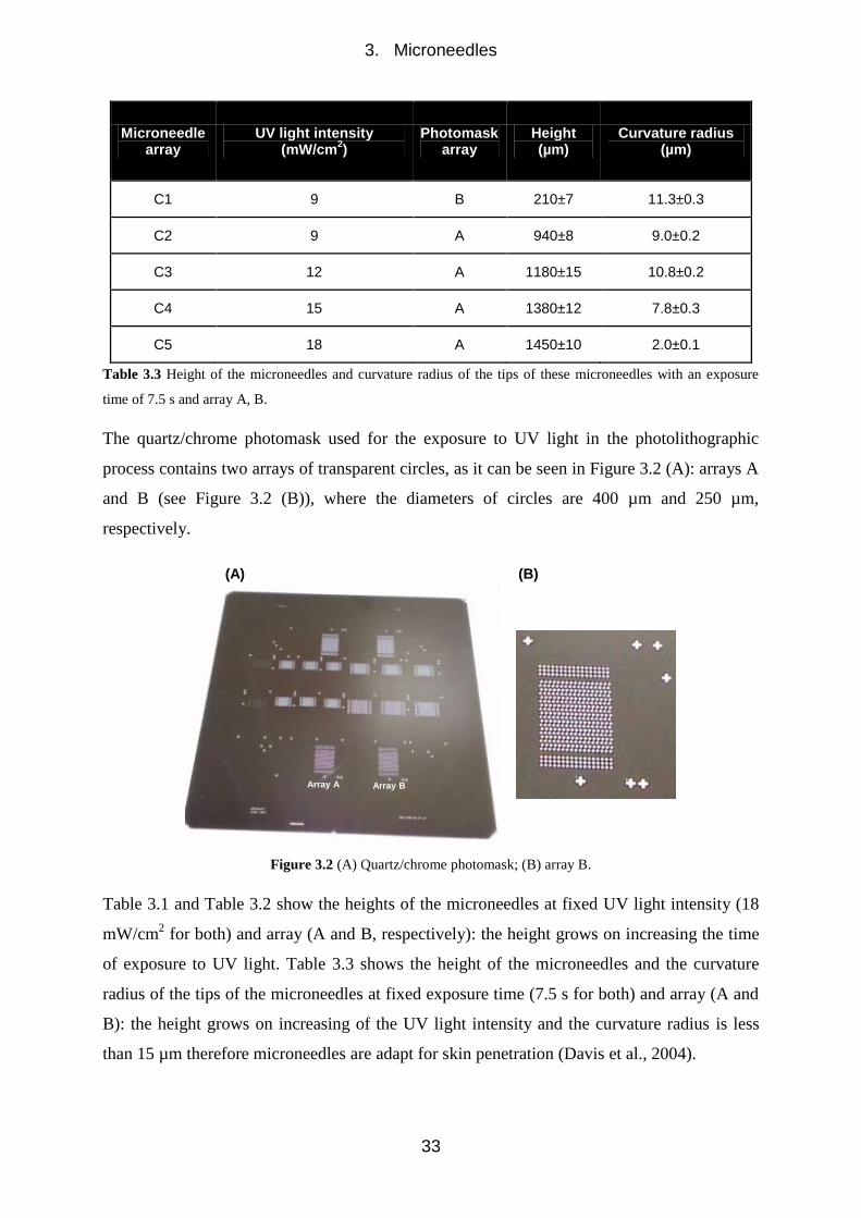
The quartz/chrome photomask used for the exposure to UV light in the photolithographic
process contains two arrays of transparent circles, as it can be seen in Figure 3.2 (A): arrays A
and B (see Figure 3.2 (B)), where the diameters of circles are 400 µm and 250 µm,
respectively.
Figure 3.2 (A) Quartz/chrome photomask; (B) array B.
Table 3.1 and Table 3.2 show the heights of the microneedles at fixed UV light intensity (18
mW/cm2 for both) and array (A and B, respectively): the height grows on increasing the time
of exposure to UV light. Table 3.3 shows the height of the microneedles and the curvature
radius of the tips of the microneedles at fixed exposure time (7.5 s for both) and array (A and
B): the height grows on increasing of the UV light intensity and the curvature radius is less
than 15 µm therefore microneedles are adapt for skin penetration (Davis et al., 2004).
Array A Array B
(A) (B)

3. Microneedles
34
3.2. Indentation hardness and skin penetration properties
The effective penetration of microneedles into the skin is a major issue, because microneedles
can broke due to uneven skin surface or human error during the penetration. Microneedles
insertion studies were typically performed in biological tissue, but this can present some
disadvantages, in that tissue samples are often heterogeneous, unstable and difficult to obtain.
In addition, the use of biological materials sometimes presents legal issues. Thus, it is
desirable to overcome these limitations by using an artificial material in place of skin. The
indentation hardness property of microneedles is compared with that of a commercial
polymeric film layer, parafilm M, used as artificial skin very similar to the surface layer of the
pig skin (Larrañeta et al., 2014). The indentation hardness is measured by means of
force/distance spectroscopy tool of the atomic force microscope (AFM). The force/distance
spectroscopy tool supports the acquisition of force vs distance curve, which is the plot of the
force, between the AFM tip and the tip of a microneedle or the parafilm M layer, as function
of their relative distance. The force spectroscopy plots show a greater slope, and thus a greater
indentation hardness, of the tip of the microneedle (see Figure 3.3 (A)) compared to that of
the parafilm M layer (see Figure 3.3 (B)).
Figure 3.3 AFM relative indentation hardness measurements of the tip of a microneedle (A) and of a parafilm M
layer (B).
This result is essential in quantify the possibility of microneedles in tissue penetration.
(A) (B)

3. Microneedles
35
In order to prove the effective insertion of microneedles into the skin, penetration test was
performed by using eight parafilm M layers folded on themselves, that mimics the pig skin
(Larrañeta et al., 2014). Figure 3.4 shows tilted (A), lateral (B) and top (C) views of the
reversed first layer, once separated from the others.
Figure 3.4 Tilted (A), lateral (B) and top (C) views of the first parafilm M layer after reversing.
It is clear that the microneedles penetrate the first layer and impress their shape, molding the
surface.
In Figure 3.5, top views of firsts five layers of the artificial skin are showed.
Figure 3.5 Optical microscope images of the first (A), the second (B), the third (C), the fourth (D) and the fifth
(E) parafilm M layer after microneedles penetration.
In particular, Figures 3.5 (A)-(E) show the holes that the same microneedles were performed
on first, second, third, fourth and fifth layer. Since each parafilm M layer is 160 µm thick,
(A) (B) (C)500 µm
(A) (B) (C)
(D) (E)
200 µm 200 µm 200 µm
200 µm200 µm

3. Microneedles
36
microneedles penetrate the first four layers for a total distance of 640 µm, proving a good
penetration strength.

4. Transdermal delivery of small molecules by microneedles based hybrid patch
37
4. Transdermal delivery of small molecules by
microneedles based hybrid patch
When oral administration of drugs is not feasible due to poor drug absorption or enzymatic
degradation in the gastrointestinal tract or liver, injection using a painful hypodermic needle is
the most common alternative. An approach that is more appealing to patients, and offers the
possibility of controlled release over time, is drug delivery across the skin using a patch
(Touitoi, 2002). However, transdermal delivery is severely limited by the inability of the large
majority of drugs to cross skin at therapeutic rates due to the great barrier imposed by skin’s
outer stratum corneum layer. To increase skin permeability, a number of different approaches
has been studied, ranging from chemical/lipid enhancers (Cevc, 2004; Williams et al., 2012)
to electric fields employing iontophoresis and electroporation (Denet et al., 2004; Kalia et al.,
2004) to pressure waves generated by ultrasound or photoacoustic effects (Doukas et al.,
2004; Mitragotri et al., 2004). Although the mechanisms are all different, these methods share
the common goal to disrupt stratum corneum structure in order to create holes big enough for
molecules to pass through. The size of disruptions generated by each of these methods is
believed to be of nanometer dimensions, which is large enough to permit transport of small
drugs and, in some cases, macromolecules, but probably small enough to prevent causing
damage of clinical significance. An alternative approach involves creating larger transport
pathways of microns dimensions using arrays of microneedles. These pathways are orders of
magnitude bigger than molecular dimensions and, therefore, should readily permit transport
of macromolecules, as well as possibly supramolecular complexes and microparticles. Despite
their very large size relative to drug dimensions, on a clinical length scale they remain small.
Although safety studies need to be performed, it is proposed that microscale holes in the skin
are likely to be safe, given that they are smaller than holes made by hypodermic needles or
minor skin abrasions encountered in daily life.
In this chapter the hybrid device based on porous silicon and polymeric microneedle array,
fabricated as described in the paragraph 2.4, is proposed as a proof-of-concept device for
transdermal drug delivery. In particular, the device operation is described and experimental
proved using it for the releasing of fluorescein molecules into a buffer solution.

4. Transdermal delivery of small molecules by microneedles based hybrid patch
38
4.1. Microneedles based hybrid patch
Hybrids device (see Figure 4.1 (A)) and patch (see Figure 4.1 (B)) based on microneedle
array and free-standing porous silicon membrane are fabricated as described in the paragraph
2.4.
Figure 4.1 Hybrids device (A) and patch (B).
The hybrid device includes a porous silicon free-standing membrane with a Bragg mirror
optical structure which reflects a specific bright color in the visible. Figure 4.2 shows the
scanning electron microscope (SEM) images of the free-standing membrane (A), made
alternating layers of low and high porosity, and the morphology of one of those two layers
(B), constituted of mesopores.
Figure 4.2 SEM images of the cross-section of the free-standing porous silicon membrane (A) and of the surface
of the porous silicon layer (B).
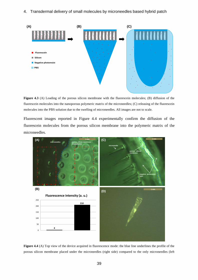
4.2. Optically monitored administration of fluorescein molecules
A sketch of the device operation is showed in Figure 4.3, where the porous silicon membrane,
that acts as drugs/molecules reservoir, is firstly loaded with the drug (see Figure 4.3 (A)), then
the drug diffuses into the polymeric matrix of the microneedles (see Figure 4.3 (B)) and,
finally, the drug is released into the external solution (see Figure 4.3 (C)). As a proof of
concept, a dye molecule, 332 Da fluorescein, and PBS solution 1X at pH 7.2 are used as drug
and external solution. PBS mimics the human interstitial fluid.
(A) (B)
(A) (B)
4. Transdermal delivery of small molecules by microneedles based hybrid patch
39
Figure 4.3 (A) Loading of the porous silicon membrane with the fluorescein molecules; (B) diffusion of the
fluorescein molecules into the nanoporous polymeric matrix of the microneedles; (C) releasing of the fluorescein
molecules into the PBS solution due to the swelling of microneedles. All images are not to scale.
Fluorescent images reported in Figure 4.4 experimentally confirm the diffusion of the
fluorescein molecules from the porous silicon membrane into the polymeric matrix of the
microneedles.
Figure 4.4 (A) Top view of the device acquired in fluorescence mode: the blue line underlines the profile of the
porous silicon membrane placed under the microneedles (right side) compared to the only microneedles (left
(A) (B) (C)
PBS
Negative photoresist
Silicon
Fluorescein
microneedles porous silicon membrane +
microneedles
4
210
0
50
100
150
200
250
Fluorescence intensity (a. u.)
microneedle
negative photoresist
layer
porous silicon
membrane
(A)
(B)
(C)
(D)
1 mm 1 mm
1 mm

4. Transdermal delivery of small molecules by microneedles based hybrid patch
40
side); (B) fluorescence intensities of the areas inside the red rectangles of (A); (C) lateral view of the device
acquired in fluorescence mode: the blue line underlines the profile of the porous silicon membrane placed under
the microneedles; (D) single microneedle detached from the device after fluorescein loading.
The migration of the luminescent molecules from porous silicon membrane to microneedles
starts just after the bonding of device constituents and spontaneously occurs also in absence of
the external solution. Top view of the device, acquired in fluorescence mode, is showed in
Figure 4.4 (A): the blue line shows the porous silicon membrane placed under the
microneedles and the only microneedles. Only the area of microneedle array overlapping the
porous silicon membrane is fluorescent. A quantitative estimation, by counting the
fluorescence intensities of the areas inside the red rectangles (see Figure 4.4 (B)), reveals an
high intensity (210 counts) for the porous silicon membrane just under the microneedle array
(see right side of the Figure 4.4 (A)) and a low intensity (4 counts) for only microneedles
outside the area of the porous silicon membrane (see left side of the Figure 4.4 (A)), also
proving that polymeric microneedles do not show intrinsic fluorescence signal. Cross section
of the whole device (see Figure 4.4 (C)) and picture of a single microneedle (see Figure 4.4
(D)), detached from the negative photoresist layer, have been acquired in fluorescence mode.
Both images show that the fluorescein is almost uniformly distributed from the base to the tip
of the microneedles: this result proves that the fluorescein molecules are not chemically
bonded neither mechanically fixed into the polymeric matrix and can easily diffuse from the
mesoporous of the membrane to the nanoporous polymeric matrix (Li et al., 2013). The
diffusion naturally stops when equilibrium between the fluorescein concentration into the
porous silicon membrane and the rest of the device is reached.
The porous silicon membrane has a double function: it acts as a drugs/molecules reservoir,
and, since its color changes depending on what fills its pores, it can be used to optically
monitor the drugs/molecules loaded and released from it. In Figure 4.5 (A), the reflectivity
spectra of the porous silicon membrane after oxidation, fluorescein loading and PBS
immersion after 2 hours are showed. The Bragg multilayer, i.e. a stack of alternating films
with proper thicknesses and refractive indexes which satisfy the Bragg relationship, is an
interferometric mirror that exhibits maximum reflection for a specific interval of wavelengths,
the so called stop band. The stop band shifts if thicknesses or refractive indexes are modified:
is this the case of porous silicon based Bragg mirror, where the stop band position depends on
the porosity of the stack. When the porous silicon membrane is filled by molecules, the
optical spectrum red shifts towards higher wavelengths, since the material appears denser on
average: in case of fluorescein loading more than 100 nm of shift can be measured (see Figure

4. Transdermal delivery of small molecules by microneedles based hybrid patch
41
4.5 (A)). The new position of the resonant wavelength is stable: the diffusion of fluorescein in
the polymeric matrix does not modify the optical spectrum, i.e. there is not a relevant
depletion of the porous silicon membrane. On the contrary, a strong blue shift (more than 50
nm) of the spectra after immersion in PBS for 2 hours proves the release of fluorescein from
the porous silicon membrane to the microneedles. The shifts of the optical spectrum
correspond to changes in color of the device from violet to green and then to blue, which can
be clearly monitored by naked eye, as showed in Figure 4.5 (B).
Figure 4.5 Spectroscopic reflectometry (A) and naked eye (B) characterizations after oxidation, fluorescein
loading and release of fluorescein in the PBS solution.
In Table 1, the spectroscopic reflectometry data relative to the absolute position of the
wavelength peak and the blue shift of Bragg optical structure peak are reported as function of
immersion time in PBS (0, 2, 4, 8 and 24 hours).
Before PBS After 2h in PBS After 4h in PBS After 8h in PBS After 24h in PBS
Peak position 508.2±0.3 450.5±0.4 444.9±0.5 445.6±0.9 436.6±0.2
Blue shift - 57.7±0.1 63.3±0.1 62.7±0.2 71.6±0.1
Table 4.1 Spectroscopic reflectometry data of absolute position and shift of Bragg optical structure peak as
function of immersion time in PBS solution.
after loading after releaseunloaded
(A)
(B)
red shift
blue shift
400 425 450 475 500 525 550 575 600 625 650
0.0
0.2
0.4
0.6
0.8
1.0
Re
fle
cti
vit
y (
a.u
.)
Wavelenght (nm)
unloaded
after loading
after release

4. Transdermal delivery of small molecules by microneedles based hybrid patch
42
The fluorescence intensity as function of immersion time in PBS (0, 2, 4, 8 and 24 hours) of
the microneedle array (see Figure 4.6) is strictly related to the blue shift of the porous silicon
membrane optical spectrum: as a matter of fact, the blue shift indicates a depletion of the
porous silicon tank, to which corresponds a decrease of the fluorescence intensity of the
microneedles as the immersion time in PBS increases. The decreasing of the fluorescence
intensity means that fluorescein molecules diffuse from the microneedles to the PBS solution.
It is verified that the fluorescence decrease is not due to a decay of the radiative properties of
the molecules by measuring the fluorescence intensity of loaded microneedles not exposed to
PBS solution as a function of time, as reported in Figure 4.6.
Figure 4.6 Changing of the fluorescence intensity of microneedles of two devices, one immersed in the PBS
solution and the other no, as function of time.
After the equilibrium is reached, the fluorescent signal does not change in time, so it is
possible to attribute the strong emission change of the device exposed to PBS solution to a
real dispersion of fluorescein in the external solution.
In order to confirm that the decreasing of microneedles fluorescence intensity is due to the
release of fluorescein in the PBS solution, those data are compared with those reported in ref.
(Donnelly et al., 2012) as showed in Figure 4.7.
0 4 8 12 16 20 241
2
3
4
5
6
7
8
9
sample exposed to PBS 1X
sample not exposed to PBS 1X
Flu
ore
sc
en
ce
in
ten
sit
y (
a.
u.)
Time (hrs)

4. Transdermal delivery of small molecules by microneedles based hybrid patch
43
Figure 4.7 Comparison between the estimated fluorescein released in PBS and data of in vitro release as
reported in ref. (Donnelly et al., 2012).
Methylene blue (320 Da) loaded in hydrogel-forming microneedles patch, made of 15% w/w
poly(methylvinylether/maelic acid) and 7.5% w/w poly(ethyleneglycol), was released and
quantified in vitro experiment (Donnelly et al., 2012). If it was assumed that the estimated
fluorescein was proportional to the complement of the fluorescence intensity, i.e. molecules
released were estimated as 1-Ifn (where Ifn is the fluorescence intensity normalized to its
maximum value), the comparison with respect to data reported in ref. (Donnelly et al., 2012)
highlighted a really similar behavior, and the kinetic of the release was also very similar.
0 4 8 12 16 20 24
0.0
0.1
0.2
0.3
0.4
0.5
0.6
0.7
0.8
0.9
1.0
Mo
lec
ule
s r
ele
as
e (
a.
u.)
Time (hrs)
estimated fluorescein released
in vitro release (from ref. Donnelly et al., 2012 modified)

5. Transdermal biosensing of biological molecules by microneedles based enzymatic electrodes
44
5. Transdermal biosensing of biological molecules by
microneedles based enzymatic electrodes
A growing general attention on public health, in particular on nutrition and sport activity,
indicated as primary prevention of diseases, such as obesity and diabetes as well as cancer,
supported a continuous development of diagnostic devices in the last ten years. Currently, the
most important physiological parameters is measured in laboratories and requires dedicate
instrumentation, not available for self-diagnostic at home. Electrochemical biosensors, and in
particular microneedles based enzymatic electrodes, offer an unique opportunity to realize
point of care microdevices with pain free, minimally invasive, low cost and minimal training
features (Ventrelli et al., 2015). The immobilization of the enzyme on the electrode with
maintained enzyme activity is the most hard task for the realization of the device. The
immobilization method influences the performances, the response time, the sensitivity, the
stability and the lifetime of the biosensor. The enzyme immobilizing method should promote
a rapid propagation of generated electrons and avoid nonspecific binding and electrode
failing. Electrode features can be optimized by using several matrices in which enzymes can
be dispersed. Among many available from material science studies, hydrogels are excellent
enzyme encapsulation materials, that avoid enzymatic binding, allow analyte molecules
diffusion and interaction with the enzymes, provide near physiologic conditions and avoid
enzymes denaturation (Yan et al., 2010). PEGDA rapidly hardens at room temperature in
presence of a photoinitiator on exposure to UV light, therefore it gives an excellent
encapsulation of the enzyme. Moreover, this peculiarity can be used to fabricate microneedles
by photolithographic process.
In this chapter two microneedles based enzymatic electrodes, realized as described in the
parahraph 2.5, are proposed as proof-of concept devices for transdermal biosensing. In
particular, the operation of the two devices is described and experimental proved for the
electrochemical detection of glucose and lactic acid molecules.
5.1. Microneedles based enzymatic electrodes
The enzymatic electrode for the detection of glucose, fabricated as described in the paragraph
2.5, is showed in the Figure 5.1.

5. Transdermal biosensing of biological molecules by microneedles based enzymatic electrodes
45
Figure 5.1 Pictures front (A) and back (B) of the microneedles based enzymatic electrode for the detection of
glucose.
The device is completely flexible, in particular the microneedle array (see Figure 5.1 (A))
could be deformed without breaking, and the back is continuously covered by gold (see
Figure 5.1 (B)), assuring a good electrical contact. The length of the microneedles is of about
500 µm. The enzymatic electrode for the detection of lactic acid is equal to this, therefore it is
not showed.
5.2. Electrochemical detection of glucose and lactic acid molecules
A scheme of the device working principle and of the experimental setup geometry is
illustrated in Figure 5.2.
Figure 5.2 (A) Sketch of the three electrode cell; (B) immersion of the three electrodes inside the electrolytic
solution, with following swelling of the microneedles; (C) penetration of the analyte molecules (glucose or lactic
(B)(A)
(A) (B) (C)
_
_
_
_
_
_
_
_
_
_
_
_
_
_
_
Electrolytic solution
Gold
Negative photoresist 2
Enzyme (GOx or LOx)
Analyte (glucose or lactic acid)
- Electron Silicone
Negative photoresist 1
Enzyme with analyte

5. Transdermal biosensing of biological molecules by microneedles based enzymatic electrodes
46
acid) inside the microneedles and redox interaction between the enzyme (GOx or LOx) and the analyte (glucose
or lactic acid), with following generation of electrons. All images are not to scale.
The setup is constituted of a three electrode cell (see Figure 5.2 (A)): a platinum wire is the
auxiliary electrode, a saturated silver chloride (silver/silver chloride 3 M) is the reference
electrode and the microneedles based enzymatic electrode (that for glucose or that for lactic
acid) is the working electrode. The three electrodes are immersed in an electrolytic solution
(see Figure 5.2 (B)), that mimics the interstitial fluid, made of PBS at 10 mM concentration
(pH 7.4) mixed with 0.48 mM magnesium chloride (MgCl2), deoxygenated with nitrogen
during the electrochemical measurements. The swelling of the polymeric matrix of the
microneedles allow to analyte molecules (glucose or lactic acid) to penetrate into the
microneedles and to interact with the enzyme (GOx or LOx) locked inside the porous matrix
(see Figure 5.2 (C)), resulting in the generation of electrons collected by auxiliary electrode.
Sensing mechanism is based on redox reactions between analyte (glucose or lactic acid) and
enzyme (GOx or LOx), summarized in equations (1)-(3) in case of glucose and equations (4)-
(6) in case of lactic acid: through these reactions, the analyte concentration is transduced into
an electrical current value (Heller et al., 2008; Wang, 2008). In particular, the biocatalytic
reaction involves reduction of enzyme flavin group (FAD) in its reduced form (FADH2),
reported in equation (1) for glucose and equation (4) for lactic acid. Glucose is oxidized to D-
glucono-1,5-lactone (equation (1)) and lactic acid is oxidized to pyruvic acid (equation (4)).
An artificial mediator, the vinylferrocene, promotes the electrons charge transfer between
FAD center and enzymatic electrode surface (equations (2) and (5) for glucose and lactic acid,
respectively): vinylferroceneox and vinylferrocenered are the oxidized and reduced forms of the
mediator. The reduced form of the mediator is then re-oxidized on the electrode, giving a
current signal (proportional to the glucose or lactic acid concentration) while regenerating the
oxidized form of the mediator (equation (3) for glucose and equation (6) for lactic acid).
( ) ( ) ( )
( ) ( ) ( )
( )
( ) ( ) ( )
( ) ( ) ( )
( )
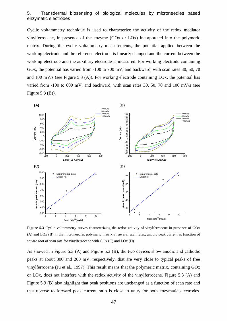
5. Transdermal biosensing of biological molecules by microneedles based enzymatic electrodes
47
Cyclic voltammetry technique is used to characterize the activity of the redox mediator
vinylferrocene, in presence of the enzyme (GOx or LOx) incorporated into the polymeric
matrix. During the cyclic voltammetry measurements, the potential applied between the
working electrode and the reference electrode is linearly changed and the current between the
working electrode and the auxiliary electrode is measured. For working electrode containing
GOx, the potential has varied from -100 to 700 mV, and backward, with scan rates 30, 50, 70
and 100 mV/s (see Figure 5.3 (A)). For working electrode containing LOx, the potential has
varied from -100 to 600 mV, and backward, with scan rates 30, 50, 70 and 100 mV/s (see
Figure 5.3 (B)).
Figure 5.3 Cyclic voltammetry curves characterizing the redox activity of vinylferrocene in presence of GOx
(A) and LOx (B) in the microneedles polymeric matrix at several scan rates; anodic peak current as function of
square root of scan rate for vinylferrocene with GOx (C) and LOx (D).
As showed in Figure 5.3 (A) and Figure 5.3 (B), the two devices show anodic and cathodic
peaks at about 300 and 200 mV, respectively, that are very close to typical peaks of free
vinylferrocene (Ju et al., 1997). This result means that the polymeric matrix, containing GOx
or LOx, does not interfere with the redox activity of the vinylferrocene. Figure 5.3 (A) and
Figure 5.3 (B) also highlight that peak positions are unchanged as a function of scan rate and
that reverse to forward peak current ratio is close to unity for both enzymatic electrodes.
(B)
-200 0 200 400 600 800-75
-60
-45
-30
-15
0
15
30
45
60
75
90
105
120
135 30 mV/s
50 mV/s
70 mV/s
100 mV/sC
urr
en
t (n
A)
E (mV) vs Ag/AgCl
(A)
-200 0 200 400 600 800-800
-600
-400
-200
0
200
400
600
800
1000
Cu
rren
t (n
A)
E (mV) vs Ag/AgCl
30 mV/s
50 mV/s
70 mV/s
100 mV/s
(D)(C)
5 6 7 8 9 10300
400
500
600
700
800
900
1000 Experimental data
Linear Fit
An
od
ic p
eak c
urr
en
t (n
A)
Scan rate1/2
(mV/s)
5 6 7 8 9 10
30
40
50
60
70 Experimental data
Linear fit
An
od
ic p
eak c
urr
en
t (n
A)
Scan rate1/2
(mV/s)

5. Transdermal biosensing of biological molecules by microneedles based enzymatic electrodes
48
Moreover, Figure 5.3 (C) and Figure 5.3 (D) demonstrate that the anodic peaks current
increases proportionally to the scan rate (R2 = 0.95 and R
2 = 0.91 respectively, R
2 being the
coefficient of linear regression) for both enzymatic electrodes. These results suggest that the
redox activity of the mediator is fast and reversible.
Chronoamperometry technique quantifies the responses, in terms of current, of the two
devices at several concentrations of glucose and lactic acid, in concentration ranges of interest
for the detection in human interstitial fluid (Shim et al., 2009; Shum et al., 2009; Yao et al.,
2011; Thomas et al., 2012). During chronoamperometry measurements, the potential between
working and reference electrodes is fixed and the current, flowing between working and
auxiliary electrodes, is measured as function of time. The chronoamperometry characteristics
are performed at 300 mV, in presence of known analyte concentrations, 5 minutes after
addition of each aliquot of analyte in order to allow the diffusion inside the electrolytic
solution. Glucose and lactic acid are detected at the following concentrations: 0, 2, 4, 6, 8, 10,
12 mM and 0, 0.2, 0.4, 0.6, 0.8, 1, 2, 3, 5, 7, 9, 12 mM, respectively. Figure 5.4 (A) and
Figure 5.4 (B) report the current-time relationship of the two devices at several concentrations
of glucose and lactic acid, respectively.
Figure 5.4 Chronoamperometry response of the microneedles based enzymatic electrodes at several
concentrations of glucose (A) and lactic acid (B); calibrations curves and fits with Michaelis-Menten model of
0 50 100 150 200 250 300 350 400100
150
200
250
300
350
400
450
500
550
600
Cu
rren
t (n
A)
Time (s)
glucose concentration
0mM
2mM
4mM
6mM
8mM
10mM
12mM
0 100 200 300 400 500 600 700 8003.03.54.04.55.05.56.06.57.07.58.08.59.09.5
10.010.511.011.512.0
lactic acid concentration
0 mM 2 mM
0.2 mM 3 mM
0.4 mM 5 mM
0.6 mM 7 mM
0.8 mM 9 mM
1 mM 12 mM
Cu
rren
t (n
A)
Time (s)
(A) (C)
(B) (D)
0 1 2 3 4 5 6 7 8 9 10 11 12
3.0
3.5
4.0
4.5
5.0
5.5
6.0
6.5
7.0
7.5
8.0 Experimental data
Michaelis-Menten fit
Cu
rre
nt
(nA
)
Lactic acid concentration (mM)
0.0 0.2 0.4 0.6 0.8 1.0
3.0
3.5
4.0
4.5
5.0
5.5
6.0
6.5
7.0
7.5
8.0
Cu
rren
t (n
A)
Lactic acid concentration (mM)
Experimental data
Linear fit
0 2 4 6 8 10 12140
160
180
200
220
240
260
280
300
320 Experimental data
Michaelis-Menten fit
Cu
rre
nt
(nA
)
Glucose concentration (mM)
0 2 4 6140
160
180
200
220
240
260
280
300
320
Cu
rren
t (n
A)
Glucose concentration (mM)
Experimental data
Linear fit

5. Transdermal biosensing of biological molecules by microneedles based enzymatic electrodes
49
the microneedles based enzymatic electrodes containing GOx (C) and LOx (D). In the inset of (C) and (D), the
linear region of the response is underlined and the linear fit is showed.
Figure 5.4 (C) and Figure 5.4 (D) illustrate the calibration curves for glucose and lactic acid,
respectively: for each analyte concentration, the stationary current value is considered. The
response of the device to glucose is linear (R2 value of 0.93) with a sensitivity of 18 ± 3 nA
mM-1
in the range from 0 to 6 mM (see inset Figure 5.4 (C)). The response of the other device
to lactic acid is linear (R2 value of 0.98) with a sensitivity of 3.5 ± 0.2 nA mM
-1 in the range
from 0 to 1 mM (see inset Figure 5.4 (D)). Response times are of the order of minutes, and
they depended on polymer nanostructure: penetration of solution in the microneedle matrix is
diffusion-driven and faster signal generation can be obtained by tuning its porosity. By using
a PEGDA with average molecular weight greater than 250, with longer polymeric chains and
wider mesh, should promote analyte penetration and fasten device response. However,
PEGDA molecular weight determines microneedles mechanical properties, such as
indentation hardness; therefore, a tradeoff between analytes diffusion and penetration of the
microneedles in human skin without breaking could limit the amount of PEGDA in the
polymeric solution. The experimental data in Figure 5.4 (C) and Figure 5.4 (D) are fitted with
Michaelis-Menten model for enzymatic kinetic behavior: I=(Imax·c) / (KM + c), where I is the
current response of the device, c is the analyte concentration and KM is the Michaelis constant.
The fits yield a KM value of 2.7 ± 0.7 mM (R2 = 0.99) in case of glucose, and 0.45 ± 0.03 mM
(R2 = 0.99) in case of lactic acid. The KM represents a measure of how strong is the
biomolecular interaction between the enzyme and the analyte: the obtained low values are
related to the high affinity between the enzyme (GOx or LOx) and analyte (glucose or lactic
acid), confirming that polymeric matrix allow the penetration of the analyte inside it and a
correct working of the enzyme, even if confined in a nanometric space. The limits of
detection, experimentally measured, is 1 µM for both the two analytes, quantifies by
respective devices.
6. Filtration of small molecules by filter based microfluidic device
50
6. Filtration of small molecules by filter based
microfluidic device
Since 1990, microfluidics has nowadays developed into a versatile technology with a huge
plethora of applications. While initially focused on liquid and gases flow through simple
channel layouts, designs of chips are much more complicated since they could include lot of
components integrated inside. Large effort has been spent into the integration of unit
operations on-chip, e.g. sample pre-treatment, mixing of different substances, controlled
chemical reaction, and separation/purification of products (Sato et al., 2003; Erickson et al.,
2004). Looking at methods used for components integration, many research groups have
started out with clever designs of silicon chips, using the well-established toolbox of
semiconductor industry. Lately, a shift toward new approaches increased, aimed to simple
straightforward integration: mainly application of functionalized coatings, adsorption beads
and filters. The use of filters in microfluidics is a topic of growing interest. Filter science and
technology is a broad and highly interdisciplinary field, where process engineering, material
science and chemistry meet all together. Exploring the boundaries of these fields offers many
opportunities, and filters have already been used for an impressive range of functions, such as
separation, purification, dialysis, and so on (Scrimgeour et al., 2011; Che et al., 2013).
Traditional methods for improving components that can perform separation inside a
microchannel include fabricating a barrier with reduced channel width (Brody et al., 1996) or
an array of posts (He et al., 1999). While these approaches are capable of providing a reusable
filter, the fabrication process can be time consuming and even expensive. Other way to
fabricate a filter is to create a packed bed column, either by packing beads (Lettieri et al.,
2003) or by in situ photopolymerization (Paustian et al., 2013). The in situ
photopolymerization allows to control the position and thickness of the filter, simply by
controlling the position and the parameters of the UV exposure. The pore size of produced
filters depends of the ratio of the quantities of components contained in the hydrogel and of
the exposure time to UV light. An additional advantage of this method is its application in
existing device formats, provided that the used material for make the device is transparent to
UV light. Disadvantages include the limited range of materials that can be applied. Filters can
be fabricated using many soft materials such as PDMS, hydrogels and so on. As already
mentioned, hydrogels based on PEGDA are particularly attractive due to the possibility of
photo-induced cross-linking by simply adding a photoinitiator in the polymer solution.

6. Filtration of small molecules by filter based microfluidic device
51
In this chapter results on the microfluidic filter, fabricated as described in the paragraph 2.6,
made inside the microfluidic device, fabricated as described in the paragraph 2.2, are
presented. Also the plastic photomask used to make filter, as described in the paragraph 2.6, is
presented. The operation of the filter is characterized allowing it to filter fluorescent
molecules of rhodamine.
6.1. Plastic photomask
The fabrication process, described in the paragraph 2.6, allows to fabricate plastic photomasks
with minimum feature achievable of about 20 μm, therefore it is particularly suitable for the
fast prototyping of microfluidic devices. A test pattern, containing lines and dots in black and
white with dimensions from 10 to 100 µm, is designed (see Figure 6.1 (A)) and transferred
onto photographic film (see Figure 6.1 (B)) using this process.
Figure 6.1 (A) Test pattern; (B) plastic photomask.
Figure 6.2 (A) shows in details the plastic photomask, in which the edge are not so straight
and well defined and there is a transition region of few microns from dark to transparent
region. Dark regions are due to the presence of small particles of a metallic silver, or dye
clouds (see Figure 6.2 (B)), developed from silver halide that have received enough white
light. It is possible to observe the film grain, that has an average thickness of 410 nm and a
roughness of 120 nm (see Figure 6.2 (C)). However in transparent regions where silver is
absent, black dots with a diameter from 0.4 to 3.2 μm are found. These defects can be
neglected for microfluidic applications.
(A) (B)

6. Filtration of small molecules by filter based microfluidic device
52
Figure 6.2 (A) Optical image of the plastic photomask; zoom (B) and thickness profile (C) of the transition from
dark to transparent regions.
6.2. Filter based microfluidic device
Most of the microfluidic devices are made of PDMS, since it combines numerous excellent
physical and chemical properties (Bartolo et al., 2008). Nevertheless, some of the properties
of PDMS strongly limit its range of applications. For example, this silicone elastomer swells
in most organic solvents that is the major constraint to its use in aqueous solutions. Moreover,
permanent modification of PDMS surfaces chemical properties is still a challenging task.
Finally, the low elastic modulus of PDMS does not allow the use of high pressure (> 1 bar)
operations. In order to overcome these problems, microfluidic devices can be fabricated using
NOA. Figure 6.3 shows the microfluidic device in NOA fabricated by soft imprint
lithography, described in the paragraph 2.2.
Figure 6.3 (A) Sketch of the microfluidic device; (B) zoom of the circuit.
Nanoports, that are plastic connectors which allow to seal plastic tubes for the injection of the
liquids, are glued on the inlets and outlets of the circuit.
(B)
(C)
(A)
200 µm
inlet
outlet
(A) (B)
200 µm

6. Filtration of small molecules by filter based microfluidic device
53
The microfluidic device is integrated with a filter, fabricated as described in the paragraph
2.6. The final microfluidic circuit, showed in Figure 6.4, is thus constituted by two channels
(height=25 µm, width=225 µm) separated by the filter with height of 25 µm and width of 50
µm.
Figure 6.4 (A) Image of the microfluidic circuit, constituted by the two channels and the filter; (B) zoom of the
circuit, where the filter separates the top channel from the bottom channel.
6.3. Optically monitored filtration of rhodamine molecules
In order to see the operation of the filter, fluorescence molecules of rhodamine 6G (R6G) are
filtered. The functioning of the filter is characterized in the following (see Figure 6.5).
Figure 6.5 Operation of the filter at Q=500 µL/min: fluorescence images (A) and intensities (B) of the two
channels as function of time.
The two channels are filled with water at flow rate Q of 500 µL/min for some minutes in
order to clean them. Then, the flow of water in the top channel is stopped (Q ~ 0) and the
same channel is left filled of water. Since water is not fluorescent, the two channels are not
top channel
bottom channel
filter
(A) (B)
200 µm100 µm
0 65 s 135 s 220 s 570 s
I II III IV V
0 100 200 300 400 500 600 700 80020
25
30
35
40
Time (s)
Fluo
resc
ence
inte
nsity
(a.
u.)
bottom channel
top channel
(B)(A)

6. Filtration of small molecules by filter based microfluidic device
54
fluorescent (see Figure 6.5 (A) I). The bottom channel is filled with an aqueous solution of
R6G at Q=500 µL/min, therefore it becomes completely fluorescent (see Figure 6.5 (A) II).
The R6G diffuses from the bottom to the top channel through the filter (see Figure 6.5 (A) III,
IV). After few minutes, the top channel is filled of the R6G (see Figure 6.5 (A) V) therefore it
becomes completely fluorescent. Figure 6.5 (B) shows the fluorescence intensities as function
of the time of the bottom and top channels: the intensities tend to become equals after a few
minutes.
The reversibility of the device is showed in Figure 6.6.
Figure 6.6 Reversibility of the filter at Q=500 µL/min: fluorescence images (A) and intensities (B) of the two
channels as function of time.
The two channels, containing an aqueous solution of R6G (Q ~ 0 in the top channel) from the
previous test, are fluorescent (see Figure 6.6 (A) I). The bottom channel is filled with water at
Q=500 µL/min, therefore it becomes completely not fluorescent (see Figure 6.6 (A) II). The
water diffuses from the bottom to the top channel through the filter (see Figure 6.6 (A) III).
After few minutes, the top channel is filled of water therefore it becomes completely not
fluorescent. Figure 6.6 (B) shows the fluorescence intensities as function of the time of the
bottom and top channels: the intensities tend to become equals after a few minutes.
The same studies were performed by tuning the solution flux at Q=100 µL/min (see Figure
6.7 and Figure 6.8).
0 85 s 715 s 1995 s
I II III IV
0 500 1000 1500 2000 250025
30
35
40
45
50
Time (s)
Fluo
resc
ence
inte
nsity
(a.
u.)
bottom channel
top channel
(A) (B)

6. Filtration of small molecules by filter based microfluidic device
55
Figure 6.7 Operation of the filter at Q=100 µL/min: fluorescence images (A) and intensities (B) of the two
channels as function of time.
Figure 6.8 Reversibility of the filter at Q=100 µL/min: fluorescence images (A) and intensities (B) of the two
channels as function of time.
The behavior of the system is very similar to the previous one and significant differences
cannot been seen.
0 65 s 95 s 235 s 650 s
I II III IV V
(B)(A)
0 200 400 600 800 1000 1200 140030
35
40
45
50
55
60
Time (s)
Fluo
resc
ence
inte
nsity
(a.
u.)
bottom channel
top channel
0 100 200 300 400 500 600 700
0 570 s 1440 s 3180 s
I II III IV
0 500 1000 1500 2000 2500 3000 35000
50
100
150
200
Time (s)
Fluo
resc
ence
inte
nsity
(a.
u.)
bottom channel
top channel
(B)(A)

7. Conclusions
56
7. Conclusions
Well established integrated circuits technologies, traditionally used in production of
microprocessors, are more and more exploited in different fields, very distant from classic
electronics, such as medicine and biology. However, transferring these technologies from the
integrated circuit industry to other scientific fields is not trivial, since it requires large efforts
to adapt traditional materials and processes to these areas or in some cases to develop and use
alternative materials and processes with respect to traditional ones. Nevertheless, the research
towards this direction offers amazing potentialities. For example, it gives a unique
opportunity to fabricate miniaturized devices for a huge variety of applications, like the
realization of microdevices that have the same functionalities of a conventional laboratory
equipment, or, in the better cases, the integration of all laboratory functions in a single
microdevice, the development of tools to make tasks in more efficient and effective way with
respect to conventional methods, and in some cases in real time and in continuous mode. The
research activity presented in this PhD thesis is placed in this contest with the aim to define
new fabrication procedures, combining lithographic processes of both hard and soft materials,
for the realization of three innovative microdevices for biomedical applications.
The firsts two microdevices, one for transdermal drug delivery and the other for transdermal
biosensing, have been fabricated by photolithography. The core of these microdevices is the
flexible microneedle array. Microneedles have been fabricated with only the
photolithographic process of a photocurable hydrogel based on PEGDA. No other step, like
thin layers deposition or etching has been used, thus making the process simple, fast and
cheap. Microneedles with several heights, bases and curvature radii of the tips have been
fabricated by changing the UV light intensity or the exposure time to UV light. The height
varies from about 200 to 2200 µm, the bases are 250 µm and 400 µm, and the curvature
radius goes from about 2 to 11 µm. Indentation hardness of the microneedles has been
compared with that of a parafilm M, used as artificial skin very similar to the surface layer of
the pig skin. Microneedles have an indentation hardness more high than that of the parafilm
M, thus they are able to penetrate into the skin. A penetration test of microneedles into eight
parafilm M layers folded on self, that mimics the pig skin, has been performed. Microneedles
penetrate the first four layers, for a total distance of 640 µm, without breaking.
The first microdevice, made of a free-standing porous silicon membrane integrated with a
microneedle array, has been realized and tested for the releasing of fluorescein molecules,
which can mimic a small drug, into a PBS solution, that mimics the human interstitial fluid.

7. Conclusions
57
The fluorescein molecules have been loaded in the porous silicon membrane, which acts as a
drug reservoir. At the same time, it allows an optical control of the drug loading since the
reflectivity spectra of the porous silicon membrane red shifts of about 100 nm. Fluorescein
molecules diffuse from the porous silicon reservoir to the microneedles: this has been
confirmed by spectroscopic reflectometry, evidencing a blue shift of about 50 nm of the
reflectivity spectra of the porous silicon membrane, and by strong fluorescence exhibited by
microneedle array. The shifts of the reflectivity spectra correspond to changes in color of the
porous silicon membrane, visible by naked eye, from violet to green and then to blue. The
diffusion of the fluorescein molecules from the microneedles into the PBS solution has been
confirmed by the continuous decreasing of the fluorescence intensity of the microneedles
during the immersion of the device in PBS solution for 2, 4, 8 and 24 hours. Migration of
fluorescein molecules from porous silicon reservoir to microneedles, and from microneedles
to PBS solution is only driven by diffusion and conditioned by material properties and
morphologies: by tuning porosities of silicon and polymer, and changing their surface
chemistries, every kind of drug (hydrophilic and lipophilic) in any interval of time (very rapid
or very slow) can be locally administrated without using any external force.
The second set of microdevices, i.e. microneedles based enzymatic electrodes, made of
microneedle arrays coated by gold, has been realized and tested for electrochemical detection
of glucose and lactic acid molecules. The microneedle array of both electrodes contains a
redox mediator, the vinylferrocene. Moreover, the microneedle array of the electrode for the
detection of glucose also contains the enzyme GOx, while the other microdevice contains the
LOx. The redox activity of the vinylferrocene, that carries electrons from the enzyme to the
surface electrode, has been checked by cyclic voltammetry. These measurements show that
anodic and cathodic peaks of vinylferrocene, immobilized inside the microneedles, are 300
mV and 200 mV, for both microdevices. These values are the typical peak values of the free
vinylferrocene, therefore the polymeric matrix and the other species contained inside the
microneedles do not affect the redox activity of vinylferrocene. The two microdevices have
been used to quantify glucose and lactic acid in PBS solutions with concentrations of analytes
in the mM range, which is the range of interest in the human interstitial fluid in physiologic
conditions. The calibration curves, i.e. current as function of analyte concentration, show
good sensitivities, 18 ± 3 nA mM-1
and 3.5 ± 0.2 nA mM-1
for the detection of glucose and
lactic acid, respectively. Since the two microdevices have an enzymatic behavior, the
experimental data of the calibration curves have been fitted by Michaelis-Mentel model: the
fits yielded a KM value of 2.7 ± 0.7 mM in case of glucose and 0.45 ± 0.03 mM in case of

7. Conclusions
58
lactic acid. The KM estimated are low, which means that there is a high affinity between the
enzyme (GOx or LOx) immobilized inside the microneedles and the analyte (glucose or lactic
acid), therefore the activity of the immobilized enzyme is not altered compared to the free
enzyme. The limit of detection, experimentally measured, is 1 µM for both the two analytes,
quantified by respective microdevices.
A homemade fabrication process, based on photographic reduction technique, of photomasks
on photographic films for fast prototyping of microfluidic devices has been developed. This
process allows the fabrication of cheap plastic photomasks, with a spatial resolution of about
20 μm.
The third microdevice, made of a microfluidic device with a microfluidic filter inside, has
been realized and tested for the filtration of fluorescent small molecules of R6G. The
microfluidic device has been realized in NOA by soft imprint lithography, that overcomes the
PDMS limits and extends the range of its applications, which is the basic material in the
microfluidic field. The device is constituted by two channels, with height of 25 µm and width
of 225 µm. The microfluidic filter has been realized inside the microfluidic device by in situ
photopolymerization of a photocurable hydrogel based on PEGDA using a homemade plastic
photomask. The advantages of this process are simplicity, speed, and versatility due to the
possibility of fabricating the filter in any location of any microfluidic circuit. Moreover, it
allows the use of several standard UV exposure systems, like a microscope coupled with a
UV lamp, a mask aligner traditionally used for photolithography or a microscope coupled to a
DMD and a UV lamp. The filter has a height of 25 µm and a width of 50 µm. The operation
of the filter has been tested: the fluorescent molecules of R6G diffuse from one channel to the
other channel through the filter, that is constituted of nanopores. Two different flow rates
have been used, in particular 100 µL/min e 500 µL/min: significant differences between them
have been not seen. Other characterizations have to be done in order to provide quantitative
parameters of the filter, like permeability, by measuring the flow rate and the diffusion time,
in order to allow the use of this microdevice for a specific biomedical application, like
microdialysis.
Even if not straightforward nor simple, the shifting of existing and mature technologies from
the consumer electronics to biomedical world can led to the creation of novel microdevices
and tools with excellent characteristics and functionalities. However, standard production of
microdevices and tools that can really replace the existing equipment and methods is still far.
For evidence of this, it can think to the computer mouse, which took 20 years to appear in the
Macintosh computer after its first prototype made in the 1960s by Engelbart. Therefore, the

7. Conclusions
59
research, both basic and applied, in this field is active and promising, and others exceptional
results can be envisaged.

8. References
60
8. References
Aoyagi, S., Izumi, H., & Fukuda, M. (2008). Biodegradable polymer needle with various tip
angles and consideration on insertion mechanism of mosquito's proboscis. Sensors and
Actuators A: Physical, 143(1), 20-28.
Ashraf, M. W., Tayyaba, S., & Afzulpurkar, N. (2011). Micro electromechanical systems
(MEMS) based microfluidic devices for biomedical applications. International journal of
molecular sciences, 12(6), 3648-3704.
Ashraf, M. W., Tayyaba, S., Nisar, A., Afzulpurkar, N., Bodhale, D. W., Lomas, T., Poyai,
A., & Tuantranont, A. (2010). Design, fabrication and analysis of silicon hollow microneedles
for transdermal drug delivery system for treatment of hemodynamic
dysfunctions. Cardiovascular Engineering, 10(3), 91-108.
Aspnes, D. E., Theeten, J. B., & Hottier, F. (1979). Investigation of effective-medium models
of microscopic surface roughness by spectroscopic ellipsometry. Physical Review B, 20(8),
3292.
Bartolo, D., Degré, G., Nghe, P., & Studer, V. (2008). Microfluidic stickers. Lab on a
Chip, 8(2), 274-279.
Betancourt, T., & Brannon-Peppas, L. (2006). Micro-and nanofabrication methods in
nanotechnological medical and pharmaceutical devices. International journal of
nanomedicine, 1(4), 483.
Bhandari, R., Negi, S., & Solzbache, F. (2008, May). A novel mask-less method of
fabricating high aspect ratio microneedles for blood sampling. In Electronic Components and
Technology Conference, 2008. ECTC 2008. 58th(pp. 1306-1309). IEEE.
Bhansali, S., & Vasudev, A. (Eds.). (2012). MEMS for biomedical applications. Elsevier.
Brody, J. P., Osborn, T. D., Forster, F. K., & Yager, P. (1996). A planar microfabricated fluid
filter. Sensors and Actuators A: Physical, 54(1), 704-708.
Campbell, P. K., Jones, K. E., Huber, R. J., Horch, K. W., & Normann, R. (1991). A silicon-
based, three-dimensional neural interface: manufacturing processes for an intracortical
electrode array. Biomedical Engineering, IEEE Transactions on, 38(8), 758-768.
Cevc, G. (2004). Lipid vesicles and other colloids as drug carriers on the skin. Advanced drug
delivery reviews, 56(5), 675-711.
Chandrasekaran, S. (2003). Characterization of surface micromachined metallic
microneedles. Microelectromechanical Systems, Journal of, 12(3), 289-295.

8. References
61
Che, J., Mach, A. J., Go, D. E., Talati, I., Ying, Y., Rao, J., Kulkarni, R. P., & Di Carlo, D.
(2013). Microfluidic purification and concentration of malignant pleural effusions for
improved molecular and cytomorphological diagnostics.
Chen, B., Wei, J., & Iliescu, C. (2010). Sonophoretic enhanced microneedles array (SEMA)-
Improving the efficiency of transdermal drug delivery. Sensors and Actuators B:
Chemical, 145(1), 54-60.
Davis, G. (2008). Microfluidics: its impact on drug discovery. Innov. Pharm. Technol., 25,
24-27.
Davis, S. P., Landis, B. J., Adams, Z. H., Allen, M. G., & Prausnitz, M. R. (2004). Insertion
of microneedles into skin: measurement and prediction of insertion force and needle fracture
force. Journal of biomechanics, 37(8), 1155-1163.
De Jong, J., Lammertink, R. G. H., & Wessling, M. (2006). Membranes and microfluidics: a
review. Lab on a Chip, 6(9), 1125-1139.
Denet, A. R., Vanbever, R., & Préat, V. (2004). Skin electroporation for transdermal and
topical delivery. Advanced drug delivery reviews, 56(5), 659-674.
Dhanekar, S., & Jain, S. (2013). Porous silicon biosensor: Current status. Biosensors and
Bioelectronics, 41, 54-64.
Donnelly, R. F., Singh, T. R. R., Garland, M. J., Migalska, K., Majithiya, R., McCrudden, C.
M., Kole, P. L., Mahmood, T. M. T., McCarthy, H. O., & Woolfson, A. D. (2012).
Hydrogel‐forming microneedle arrays for enhanced transdermal drug delivery. Advanced
functional materials, 22(23), 4879-4890.
Donnelly, R. F., Singh, T. R. R., Tunney, M. M., Morrow, D. I., McCarron, P. A., O’Mahony,
C., & Woolfson, A. D. (2009). Microneedle arrays allow lower microbial penetration than
hypodermic needles in vitro. Pharmaceutical research, 26(11), 2513-2522.
Doukas, A. G., & Kollias, N. (2004). Transdermal drug delivery with a pressure
wave. Advanced drug delivery Reviews, 56(5), 559-579.
Erickson, D., & Li, D. (2004). Integrated microfluidic devices. Analytica Chimica
Acta, 507(1), 11-26.
Gates, B. D., Xu, Q., Stewart, M., Ryan, D., Willson, C. G., & Whitesides, G. M. (2005).
New approaches to nanofabrication: molding, printing, and other techniques. Chemical
reviews, 105(4), 1171-1196.
He, B., Tan, L., & Regnier, F. (1999). Microfabricated filters for microfluidic analytical
systems. Analytical Chemistry, 71(7), 1464-1468.

8. References
62
Heller, A., & Feldman, B. (2008). Electrochemical glucose sensors and their applications in
diabetes management. Chemical reviews, 108(7), 2482-2505.
Ju, H., & Leech, D. (1997). Electrochemistry of poly (vinylferrocene) formed by direct
electrochemical reduction at a glassy carbon electrode. Journal of the Chemical Society,
Faraday Transactions, 93(7), 1371-1375.
Kalia, Y. N., Naik, A., Garrison, J., & Guy, R. H. (2004). Iontophoretic drug
delivery. Advanced drug delivery reviews, 56(5), 619-658.
Kochhar, J. S., Goh, W. J., Chan, S. Y., & Kang, L. (2013). A simple method of microneedle
array fabrication for transdermal drug delivery. Drug development and industrial
pharmacy, 39(2), 299-309.
Langer, R. (2001). Drugs on target. Science, 293(5527), 58-59.
Larrañeta, E., Moore, J., Vicente-Pérez, E. M., González-Vázquez, P., Lutton, R., Woolfson,
A. D., & Donnelly, R. F. (2014). A proposed model membrane and test method for
microneedle insertion studies. International journal of pharmaceutics, 472(1), 65-73.
Lee, J. W., Park, J. H., & Prausnitz, M. R. (2008). Dissolving microneedles for transdermal
drug delivery. Biomaterials, 29(13), 2113-2124.
Lettieri, G. L., Dodge, A., Boer, G., de Rooij, N. F., & Verpoorte, E. (2003). A novel
microfluidic concept for bioanalysis using freely moving beads trapped in recirculating
flows. Lab on a Chip, 3(1), 34-39.
Li, H., Yu, Y., Faraji Dana, S., Li, B., Lee, C. Y., & Kang, L. (2013). Novel engineered
systems for oral, mucosal and transdermal drug delivery. Journal of drug targeting, 21(7),
611-629.
Lipomi, D. J., Martinez, R. V., Cademartiri, L., & Whitesides, G. M. (2012). 7.11-Soft
Lithographic Approaches to Nanofabrication. Polymer Science: A Comprehensive Reference,
Ed. K. Matyjaszewski and M. Möller, Elsevier, Amsterdam.
Liu, Y., Eng, P. F., Guy, O. J., Roberts, K., Ashraf, H., & Knight, N. (2013). Advanced deep
reactive-ion etching technology for hollow microneedles for transdermal blood sampling and
drug delivery. IET nanobiotechnology, 7(2), 59-62.
Matteucci, M., Casella, M., Bedoni, M., Donetti, E., Fanetti, M., De Angelis, F., Gramatica,
F., & Di Fabrizio, E. (2008). A compact and disposable transdermal drug delivery
system. Microelectronic Engineering, 85(5), 1066-1073.
McDonald, J. C., & Whitesides, G. M. (2002). Poly (dimethylsiloxane) as a material for
fabricating microfluidic devices. Accounts of chemical research, 35(7), 491-499.

8. References
63
Mehta, G., Lee, J., Cha, W., Tung, Y. C., Linderman, J. J., & Takayama, S. (2009). Hard top
soft bottom microfluidic devices for cell culture and chemical analysis. Analytical
chemistry, 81(10), 3714-3722.
MicroChem. www.microchem.com
Milewski, M., Brogden, N. K., & Stinchcomb, A. L. (2010). Current aspects of formulation
efforts and pore lifetime related to microneedle treatment of skin. Expert opinion on drug
delivery, 7(5), 617-629.
Mitragotri, S., & Kost, J. (2004). Low-frequency sonophoresis: a review. Advanced drug
delivery reviews, 56(5), 589-601.
Mukerjee, E. V., Collins, S. D., Isseroff, R. R., & Smith, R. L. (2004). Microneedle array for
transdermal biological fluid extraction and in situ analysis. Sensors and Actuators A:
Physical, 114(2), 267-275.
Norland Products. www.norlandprod.com
Nunes, G. S., & Marty, J. L. (2006). Immobilization of enzymes on electrodes.
In Immobilization of Enzymes and Cells (pp. 239-250). Humana Press.
Oh, J. H., Park, H. H., Do, K. Y., Han, M., Hyun, D. H., Kim, C. G., Kim, C. H., Lee, S. S.,
Hwang, S. J., Shin, S. C., & Cho, C. W. (2008). Influence of the delivery systems using a
microneedle array on the permeation of a hydrophilic molecule, calcein. European Journal of
Pharmaceutics and Biopharmaceutics, 69(3), 1040-1045.
Oh, J. K. (2009). Engineering of nanometer-sized cross-linked hydrogels for biomedical
applications. Canadian Journal of Chemistry, 88(3), 173-184.
Ottosen, R. M. (1999). Replication and compression of surface structures with
polydimethylsiloxane elastomer. Journal of Chemical Education, 76(4), 537.
Paustian, J. S., Azevedo, R. N., Lundin, S. T. B., Gilkey, M. J., & Squires, T. M. (2013).
Microfluidic microdialysis: spatiotemporal control over solution microenvironments using
integrated hydrogel membrane microwindows. Physical Review X, 3(4), 041010.
Pishko, M. V., Michael, A. C., & Heller, A. (1991). Amperometric glucose microelectrodes
prepared through immobilization of glucose oxidase in redox hydrogels. Analytical
Chemistry, 63(20), 2268-2272.
Qin, D., Xia, Y., & Whitesides, G. M. (2010). Soft lithography for micro-and nanoscale
patterning. Nature protocols, 5(3), 491-502.
Quake, S. R., & Scherer, A. (2000). From micro-to nanofabrication with soft
materials. Science, 290(5496), 1536-1540.

8. References
64
Rajaraman, S., & Henderson, H. T. (2005). A unique fabrication approach for microneedles
using coherent porous silicon technology. Sensors and Actuators B: Chemical, 105(2), 443-
448.
Rogers, J. A., & Nuzzo, R. G. (2005). Recent progress in soft lithography. Materials
today, 8(2), 50-56.
Sachdeva, V., & K Banga, A. (2011). Microneedles and their applications. Recent patents on
drug delivery & formulation, 5(2), 95-132.
Sailor, M. J. (2012). Porous silicon in practice: preparation, characterization and
applications. John Wiley & Sons.
Sato, K., Hibara, A., Tokeshi, M., Hisamoto, H., & Kitamori, T. (2003). Microchip-based
chemical and biochemical analysis systems. Advanced Drug Delivery Reviews, 55(3), 379-
391.
Scrimgeour, J., Cho, J. K., Breedveld, V., & Curtis, J. (2011). Microfluidic dialysis cell for
characterization of macromolecule interactions. Soft Matter, 7(10), 4762-4767.
Shibata, T., Nakanishi, A., Sakai, T., Kato, N., Kawashima, T., Mineta, T., & Makino, E.
(2007, June). Fabrication and mechanical characterization of microneedle array for cell
surgery. In Solid-State Sensors, Actuators and Microsystems Conference, 2007.
TRANSDUCERS 2007. International (pp. 719-722). IEEE.
Shim, N. Y., Bernards, D. A., Macaya, D. J., DeFranco, J. A., Nikolou, M., Owens, R. M., &
Malliaras, G. G. (2009). All-plastic electrochemical transistor for glucose sensing using a
ferrocene mediator. Sensors, 9(12), 9896-9902. Shum, A. J., Cowan, M., Lähdesmäki, I., Lingley, A., Otis, B., & Parviz, B. A. (2009,
August). Functional modular contact lens. In SPIE NanoScience+ Engineering (pp. 73970K-
73970K). International Society for Optics and Photonics.
Smith, R. L., & Collins, S. D. (1992). Porous silicon formation mechanisms. Journal of
Applied Physics, 71(8), R1-R22.
Sze, S. M. (2008). Semiconductor devices: physics and technology. John Wiley & Sons.
Thomas, N., Lähdesmäki, I., & Parviz, B. A. (2012). A contact lens with an integrated lactate
sensor. Sensors and Actuators B: Chemical, 162(1), 128-134.
Touitou, E. (2002). Drug delivery across the skin. Expert opinion on biological therapy, 2(7),
723-733.
Tsuchiya, K., Nakanishi, N., Uetsuji, Y., & Nakamachi, E. (2005). Development of blood
extraction system for health monitoring system. Biomedical microdevices, 7(4), 347-353.

8. References
65
Valdés-Ramírez, G., Windmiller, J. R., Claussen, J. C., Martinez, A. G., Kuralay, F., Zhou,
M., Zhou, N., Polsky, R., Miller, P. R., Narayan, R., & Wang, J. (2012). Multiplexed and
switchable release of distinct fluids from microneedle platforms via conducting polymer
nanoactuators for potential drug delivery. Sensors and Actuators B: Chemical, 161(1), 1018-
1024.
Ventrelli, L., Marsilio Strambini, L., & Barillaro, G. (2015). Microneedles for transdermal
biosensing: current picture and future direction. Advanced healthcare materials, 4(17), 2606-
2640.
Wang, J. (2008). Electrochemical glucose biosensors. Chemical reviews, 2008, 108(2), 814-
825.
Wilke, N., Hibert, C., O’Brien, J., & Morrissey, A. (2005). Silicon microneedle electrode
array with temperature monitoring for electroporation. Sensors and Actuators A:
Physical, 123, 319-325.
Williams, A. C., & Barry, B. W. (2012). Penetration enhancers. Advanced drug delivery
reviews, 64, 128-137.
Yan, J., Pedrosa, V. A., Simonian, A. L., & Revzin, A. (2010). Immobilizing enzymes onto
electrode arrays by hydrogel photolithography to fabricate multi-analyte electrochemical
biosensors. ACS applied materials & interfaces, 2(3), 748-755.
Yao, H., Shum, A. J., Cowan, M., Lähdesmäki, I., & Parviz, B. A. (2011). A contact lens with
embedded sensor for monitoring tear glucose level. Biosensors and Bioelectronics, 26(7),
3290-3296.
Ziaie, B., Baldi, A., Lei, M., Gu, Y., & Siegel, R. A. (2004). Hard and soft micromachining
for BioMEMS: review of techniques and examples of applications in microfluidics and drug
delivery. Advanced drug delivery reviews, 56(2), 145-172.

Appendix A - Lists of publications and research experiences in external labs related to the PhD work
66
Appendix A - Lists of publications and research
experiences in external labs related to the PhD work
List of publications
Journals
J5. Caliò, A., Dardano, P., Di Palma, V., Bevilacqua, M. F., Di Matteo, A., Iuele, H., & De
Stefano, L. (2016). Polymeric microneedles based enzymatic electrodes for electrochemical
biosensing of glucose and lactic acid. Sensors and Actuators B: Chemical, submitted paper.
J4. Dardano, P., Caliò, A., Politi, J., Rea, I., Rendina, I., & De Stefano, L. (2016). Optically
monitored drug delivery patch based on porous silicon and polymer microneedles. Biomedical
Optics Express, accepted paper.
J3. Caliò, A., Leng, J., Decock, J., De Stefano, L., & Salmon, J. B. (2015). Microscopy
assisted fabrication of a hydrogel-based microfluidic filter. Journal of the European Optical
Society-Rapid publications, 10. doi: 10.2971/jeos.2015.15058
J2. Dardano, P., Caliò, A., Di Palma, V., Bevilacqua, M. F., Di Matteo, A., & De Stefano, L.
(2015). A photolithographic approach to polymeric microneedles array fabrication. Materials,
8(12), 8661-8673. doi: 10.3390/ma8125484
J1. Orabona, E., Caliò, A., Rendina, I., Stefano, L. D., & Medugno, M. (2013). Photomasks
fabrication based on optical reduction for microfluidic applications. Micromachines, 4(2),
206-214. doi: 10.3390/mi4020206
Proceedings
P3. Dardano, P., Rea, I., De Stefano, L., Caliò, A., & Politi, J., Optically controlled drug
delivery system based on porous silicon and microneedles patch. In NANOfIM 2015, 1st
Workshop on Nanotechnology in Instrumentation and Measurement, Lecce, 24-25 July 2015.
ISBN 978-1-5108-1501-8
P2. Dardano, P., Caliò, A., Politi, J., Di Palma, V., Bevilacqua, M. F., Rea, I., Casalino, M.,
Di Matteo, A., Rendina, I., & De Stefano, L. (2015, June). Hybrid microneedles devices for
diagnostic and therapeutic applications: fabrication and preliminary results. In SPIE
Microtechnologies (pp. 95180L-95180L). International Society for Optics and Photonics.
doi:10.1117/12.2178919
P1. Dardano, P., Caliò, A., Politi, J., Rea, I., De Stefano, L., Di Palma, V., Bevilacqua, M. F.,

Appendix A - Lists of publications and research experiences in external labs related to the PhD work
67
& Di Matteo, A. (2015, February). Diagnostic and therapeutic devices based on polymeric
microneedles: fabrication and preliminary results. In AISEM Annual Conference, 2015
XVIII (pp. 1-4). IEEE. doi:10.1109/AISEM.2015.7066782
List of research experiences in external labs
E2. Visiting student: Laboratory of the future - Solvay, Pessac (France)
Period: 03/01/2015 - 06/30/2015
Scientific supervisors: Jacques Leng, Jean-Baptiste Salmon
Research field: microfluidics
E1. Visiting student: STMicroelectronics, Arzano (Italy)
Period: once a week from 03/01/2013 to 02/29/2016
Scientific supervisors: Andrea Di Matteo, Vincenza Di Palma
Research field: microelectronics

Appendix B - List of publications related to the other research activities investigated during the PhD program
68
Appendix B - List of publications related to the other
research activities investigated during the PhD program
List of publications
Book chapter
B1. De Stefano, L., Rea, I., Caliò, A., Politi, J., Terracciano, M., & Korotcenkov, G. (2015).
Porous silicon-based optical chemical sensors. Porous silicon: from formation to application:
biomedical and sensor applications, volume two: Biomedical and sensor applications, 69.
doi: 10.1201/b19205
Journals
J5. Politi, J., Dardano, P., Caliò, A., Iodice, M., Rea, I., & De Stefano, L. (2016). Lysine
modified oligopeptides allow reversible sensing of lead (II) ions on chip. Biosensors and
Bioelectronics, submitted paper.
J4. Della Ventura, B., Rea, I., Caliò, A., Giardina, P., Gravagnuolo, A. M., Funari, R.,
Altucci, C., Velotta, R., & De Stefano, L. (2016). Vmh2 hydrophobin layer entraps glucose: a
quantitative characterization by label-free optical and gravimetric methods. Applied Surface
Science, 364, 201-207. doi:10.1016/j.apsusc.2015.12.080
J3. Casalino, M., Coppola, G., De Stefano, L., Caliò, A., Rea, I., Mocella, V., Dardano, P.,
Romano, S., Rao, S., & Rendina, I. (2015). New perspectives in silicon micro and
nanophotonics. Journal of the European Optical Society-Rapid publications, 10. doi:
10.2971/jeos.2015.15029
J2. Caliò, A., Cassinese, A., Casalino, M., Rea, I., Barra, M., Chiarella, F., & De Stefano, L.
(2015). Hybrid organic–inorganic porous semiconductor transducer for multi-parameters
sensing. Journal of The Royal Society Interface, 12(108), 20141268.
doi: 10.1098/rsif.2014.1268
J1. Caliò, A., Rea, I., Politi, J., Giardina, P., Longobardi, S., & De Stefano, L. (2013). Hybrid
bio/non-bio interfaces for protein-glucose interaction monitoring. Journal of Applied
Physics, 114(13), 134904. doi: 10.1063/1.4824379
Proceedings
P7. Rea, I., Terracciano, M., Politi, J., Caliò, A., Dardano, P., Gioffrè, M., Lamberti, A.,

Appendix B - List of publications related to the other research activities investigated during the PhD program
69
Rendina, I., & De Stefano, L. (2015, October). Natural and synthetic nanostructured materials
for biomedical applications. In 2015 AEIT International Annual Conference (AEIT)(pp. 1-6).
IEEE. doi:10.1109/AEIT.2015.7415279
P6. Caliò, A., Cassinese, A., Casalino, M., Politi, J., Barra, M., & De Stefano, L. (2015,
May). Hybrid organic-inorganic semiconductor transducer for optical and electrical sensing.
In SPIE Optics+Optoelectronics (pp. 95061R-95061R). International Society for Optics and
Photonics. doi:10.1117/12.2178017
P5. Politi, J., Caliò, A., Dardano, P., Iodice, M., Rea, I., & De Stefano, L. (2014).
Bioconjugation of heavy metal-binding proteins on surface: an optical and gravimetric
characterization. Procedia Engineering, 87, 292-295. doi:10.1016/j.proeng.2014.11.665
P4. Caliò, A., Politi, J., Rea, I., & De Stefano, L. (2014, May). Hydrophobin-glucose
interaction monitored by porous silicon optical multi-layers hybrid interfaces for sugar-
proteins interaction monitoring. In Photonics Technologies, 2014 Fotonica AEIT Italian
Conference on (pp. 1-4). IEEE. doi:10.1109/Fotonica.2014.6843956
P3. Caliò, A., Cassinese, A., Barra, M., Rea, I., & De Stefano, L. (2014, May). PDIF-CN2
modified porous silicon optical and electrical transducers for biochemical sensing electrical
and optical sensing by porous silicon devices. In Photonics Technologies, 2014 Fotonica
AEIT Italian Conference on (pp. 1-4). IEEE. doi:10.1109/Fotonica.2014.6843900
P2. Rea, I., Caliò, A., Terracciano, M., Politi, J., De Stefano, L., & Rendina, I., Porous
silicon based photonic structures for optical monitoring of biochemical interactions. In
Fotonica 2013, 15° Convegno Nazionale delle Tecnologie Fotoniche, Milano, 21-23 May
2013. ISBN 9788887237160, ISBN-A 10.978.8887237/160
P1. De Stefano, L., Caliò, A., Politi, J., Giardina, P., Redina, I., & Rea, I. (2013, May).
Hybrid interfaces for a new class of optical biosensors. In SPIE Optics+Optoelectronics (pp.
87741G-87741G). International Society for Optics and Photonics. doi:10.1117/12.2017615

70

71
È la volontà che fa l’uomo grande o piccolo.
Johann Christoph Friedrich von Schiller

72