University of Central Florida Senior Design Group D
153
i Emergency Vehicle Alert Device University of Central Florida Senior Design Group D Spring 2010 – Fall 2010 Charles Logan, Derrick Nelson, Joshua Guinn, & Stephen Watson Dec 10 th , 2010
Transcript of University of Central Florida Senior Design Group D

i
Emergency Vehicle Alert Device
University of Central Florida
Senior Design Group D Spring 2010 – Fall 2010
Charles Logan, Derrick Nelson, Joshua Guinn, & Stephen Watson
Dec 10
th, 2010

ii
Table of Contents
1. Introduction ................................................................................. 1
1. 1 Executive Summary ................................................................................... 1
1. 2 Motivation ................................................................................................... 2
1. 3 Project Management .................................................................................. 3
1. 3. 1 Responsibilities Flowchart ................................................................... 3
1. 3. 2 Milestone Schedule for Project Completion ........................................ 5
1. 3. 3 Proposed Budget ................................................................................ 6
2. Design Specifications & Requirements .................................... 8
2. 1 Specifications ............................................................................................. 8
2. 1. 1 EAT – Emergency Alert Transmitter .................................................... 8
2. 1. 1. 1 PCM – Power Control Module ..................................................... 8
2. 1. 1. 2 TOD – Turn On Device ................................................................ 8
2. 1. 1. 3 HEC/GPS – Hall-effect Compass / GPS ...................................... 9
2. 1. 1. 4 TCU – Transmitter Control Unit ................................................... 9
2. 1. 1. 5 ETD – Emergency Transmission Device ..................................... 9
2. 1. 2 EAR – Emergency Alert Receiver ....................................................... 9
2. 1. 2. 1 PCM – Power Control Module ..................................................... 9
2. 1. 2. 2 TOD – Turn On Device .............................................................. 10
2. 1. 2. 3 HEC/GPS – Hall-Effect Compass/GPS...................................... 10
2. 1. 2. 4 RCU – Receiver Control Unit ..................................................... 10
2. 1. 2. 5 SBU – Switching Bypass Unit .................................................... 10
2. 1. 2. 6 RAA – Recorded Audible Alert ................................................... 11
2. 1. 2. 7 VDU – Visual Display Unit ......................................................... 11
2. 1. 2. 8 ERD – Emergency Receiver Device .......................................... 11
2. 2 Block Diagram .......................................................................................... 11
2. 2. 1 EAT - Emergency Alert Transmitter .................................................. 11
2. 2. 2 EAR - Emergency Alert Receiver ...................................................... 12
2. 3 Functional Requirements.......................................................................... 13
2. 3. 1 EAT – Emergency Alert Transmitter .................................................. 13
2. 3. 1. 1 PCM – Power Control Module ................................................... 14
2. 3. 1. 2 TOD – Turn On Device .............................................................. 14
2. 3. 1. 3 HEC/GPS – Hall Effect Compass / GPS .................................... 14

iii
2. 3. 1. 4 TCU – Transmitter Control Unit ................................................. 15
2. 3. 1. 5 ETD – Emergency Transmission Device ................................... 15
2. 3. 2 EAR – Emergency Alert Receiver ..................................................... 17
2. 3. 2. 1 PCM – Power Control Module ................................................... 17
2. 3. 2. 2 TOD – Turn On Device .............................................................. 17
2. 3. 2. 3 HEC/GPS – Hall Effect Compass/GPS ...................................... 18
2. 3. 2. 4 RCU – Receiver Control Unit ..................................................... 18
2. 3. 2. 5 SBU – Switching Bypass Unit .................................................... 18
2. 3. 2. 6 RAA – Recorded Audible Alert ................................................... 19
2. 3. 2. 7 VDU – Visual Display Unit ......................................................... 19
3. Research ................................................................................... 23
3. 1 Research Methodology ............................................................................ 23
3. 2 EAT – Emergency Alert Transmitter ......................................................... 24
3. 2. 1 PCM – Power Control Module ........................................................... 24
3. 2. 1. 1 Simple Resistive Voltage Divider Topology ............................... 24
3. 2. 1. 2 Shunt Regulator Topology ......................................................... 24
3. 2. 1. 3 Linear Regulator Topology......................................................... 25
3. 2. 1. 4 Switching Regulator Topology ................................................... 26
3. 2. 1. 5 Topology Evaluation and Design Criteria ................................... 26
3. 2. 2 HEC/GPS – Hall Effect Compass / GPS ........................................... 27
3. 2. 2. 1 Hall Effect Compass .................................................................. 27
3. 2. 2. 2 Global Positioning Sensor .......................................................... 30
3. 2. 3 TCU – Transmitter Control Unit ......................................................... 33
3. 2. 3. 1 FPGA – Field Programmable Gate Array................................... 34
3. 2. 3. 2 Microcontroller ........................................................................... 37
3. 2. 3. 3 Standard Logic Components ..................................................... 39
3. 2. 3. 4 Transmitter Control Unit Part Selection ..................................... 42
3. 2. 4 ETD – Emergency Transmission Device ........................................... 43
3. 3 EAR – Emergency Alert Receiver ............................................................ 51
3. 3. 1 PCM – Power Control Module ........................................................... 52
3. 3. 2 TOD – Turn On Device ..................................................................... 52
3. 3. 3 HEC/GPS – Hall Effect Compass/GPS ............................................. 52
3. 3. 4 RCU – Receiver Control Unit ............................................................ 52

iv
3. 3. 5 SBU – Switching Bypass Unit ........................................................... 53
3. 3. 6 RAA – Recorded Audible Alert .......................................................... 54
3. 3. 7 VDU – Visual Display Unit ................................................................. 57
3. 3. 8 ERD – Emergency Receiver Device ................................................. 58
3. 4. Legal Restrictions - FCC Regulations ..................................................... 61
3. 4. 1 Access to Spectrum .......................................................................... 61
3. 4. 2 Unlicensed Low Power Operation ..................................................... 63
3. 4. 3 Frequency Bands .............................................................................. 64
3. 4. 3. 1 AM and FM Radio Bands ........................................................... 64
3. 4. 3. 2 Citizens‟ Band (CB) ................................................................... 64
3. 4. 3. 3 Radar Bands .............................................................................. 65
3. 4. 3. 4 Public Safety Bands ................................................................... 65
3. 4. 3. 5 Restricted Bands ....................................................................... 65
3. 4. 4 Equipment Compliance ..................................................................... 66
3. 4. 4. 1 Classification .............................................................................. 67
3. 4. 4. 2 Operation ................................................................................... 68
3. 4. 5 Analysis and Final Determination ...................................................... 68
3. 5. Similar Projects ....................................................................................... 69
3. 5. 1. 3M Opticom Infrared System ........................................................... 69
3. 5. 2 UCF, Senior Design Group 5, Fall 2006-Spring 2007 ...................... 70
3. 5. 3 UCF, Senior Design Group 1, Fall 2007-Spring 2008 ....................... 70
3. 5. 4 UCF, Senior Design Group 3, Fall 2007-Spring 2008 ....................... 70
4. Design ........................................................................................ 71
4. 1 Design Methodology ................................................................................. 71
4. 2 Design of the Emergency Alert Transmitter .............................................. 71
4. 2. 1 Power Control Module ....................................................................... 71
4. 2. 2 Beginning of Operation – Turn on Device (TOD) .............................. 72
4. 2. 3. 1 Interfacing the Compass to the Transmitter Control Unit ........... 73
4. 2. 4 Design of Modulator and Transmitter Antenna .................................. 83
4. 3 Design of Emergency Alert Receiver ........................................................ 85
4. 3. 1 Power Control Module of Receiver.................................................... 86
4. 3. 2 Receiving the Signal – The Reception Antenna ................................ 87

v
4. 3. 4 Interface of Audio/Visual Warnings ................................................... 93
4. 3. 4. 1 Interfacing the Recorded Audible Alert ...................................... 93
4. 3. 4. 2 Interface of Visual Display Unit .................................................. 96
5. Prototype ................................................................................. 101
5. 1 Acquiring Parts: Emergency Alert Transmitter ........................................ 101
5. 2 Acquiring Parts Emergency Alert Receiver............................................. 101
5. 3 Assembly ................................................................................................ 103
5. 4 Printed Circuit Board Design .................................................................. 103
5. 5 Housing Design ...................................................................................... 104
6. Testing ..................................................................................... 105
6. 1 Component Testing ................................................................................ 105
6. 1. 1 Power Control Module ..................................................................... 105
6. 1. 2 Hall-effect Compass ........................................................................ 106
6. 1. 3 Switching Bypass Unit ..................................................................... 107
6. 1. 4 PIC .................................................................................................. 108
6. 1. 4. 1 Transmitter Control Unit ........................................................... 108
6. 1. 4. 2 Receiver Control Unit ............................................................... 109
6. 1. 5 Recorded Audible Alert ................................................................... 110
6. 1. 6 Visual Display Unit .......................................................................... 110
6. 1. 7 Transmitter/Receiver ....................................................................... 111
6. 2 Bench Testing ........................................................................................ 112
6.3 Final Testing ............................................................................................ 113
7. Operation Manual ................................................................... 115
7.1 Installation ............................................................................................... 115
7.2 Operation................................................................................................. 115
7. 2. 1 EAT ................................................................................................. 115
7. 2. 2 EAR ................................................................................................. 115
8. Design Summary .................................................................... 117
8.1 Turn-On Device ....................................................................................... 119
8.2 Power Control Modules ........................................................................... 119
8.3 Hall-Effect Compass ................................................................................ 121
8.4 GPS Modules .......................................................................................... 122
8.5 Transmitter Control Unit .......................................................................... 124

vi
8.6 Transmitter, Receiver, Antenna ............................................................... 125
8.6.1 Transmitter ........................................................................................ 125
8.6.2 Antenna, Receiver............................................................................. 126
8.7 Receiver Control Unit .............................................................................. 127
8.8 Recorded Audible Alert ........................................................................... 129
8.9 Visual Display Unit .................................................................................. 130
8.10 Switching Bypass Unit ........................................................................... 133
9. Summary and Conclusion ...................................................... 135
A. Appendices ................................................................................. A
A-1. Visual Display Settings by Directional Heading ......................................... A
A-2. Works Consulted ....................................................................................... E
A-3. Permissions ...............................................................................................H

1
1. Introduction
1. 1 Executive Summary
In today‟s bustling world, the streets are filled with a steady stream of vehicles, creating an unpredictable flow of traffic. For modern emergency vehicle drivers, this creates a daunting obstacle to navigate, especially since modern technology is constantly creating new distractions like cell phones and music players that can quickly take a driver‟s attention off of the road. These distractions are making lights and sirens, the current method of warning drivers of an approaching emergency vehicle, less and less effective, creating the need for a more advanced warning system.
The purpose of this senior design project is to create a possible solution to the problem of giving drivers a more advanced warning of an approaching emergency vehicle so that drivers can take appropriate action to let the vehicle through. When an emergency vehicle turns on its lights and sirens, the emergency alert transmitter is triggered to begin sending out a signal that will alert nearby drivers. The signal from the emergency vehicle will be picked up by the emergency alert receiver in all cars in the area, triggering the receiver to use several methods to alert the driver. The first method of alerting the driver is by shutting off the radio, CD, or other audio input of the car and playing back a pre-recorded message in both English and Spanish, informing the driver what type of emergency vehicle (ambulance, fire truck, police, etc.) is approaching. Finally, the receiver also displays an alert message on the dashboard of the vehicle, primarily meant to gain the attention of any hearing impaired drivers or any vehicles without working audio equipment.
The project also includes more intricate features to our alert system, namely a Hall-effect compass and GPS to determine which direction the emergency vehicle is approaching from in order to alert the driver if the vehicle is coming from behind them or if they need to stop because the vehicle is approaching an intersection from a different direction. This also helps to determine if the vehicle is headed away from the car, in which case the receiver would not need to alert the driver.
The design for the project is efficient, small, and cheap enough to be practical for all vehicles in order to give a more advanced notice of an approaching emergency vehicle. It should be practical for any make or model of car so that it could be implemented in any vehicle that is on the road. With powerful technology such as this project in every motorized vehicle, the roads will be made safer as well as help save time for emergency vehicles, which in many instances could mean the difference between life and death.

2
1. 2 Motivation
When considering ideas for the senior design project, there were several varying proposals which all shared one common aspect: the design needed to meet a need in the everyday life of an ordinary American citizen. When considering the pros and cons of the various proposals, various ideas were slowly eliminated as being too intricate for the level of experience and budget available or not involving enough design or practicality. As we began doing more research into the viability of the different proposals, no idea matched the level of design necessary within the available budget while satisfying a practical need in everyday life like the idea for an advanced emergency alert system.
The idea for the project came while observing an emergency vehicle approaching an intersection. The lights were flashing and the sirens blaring, yet none of the other vehicles waiting at the traffic signal seemed to notice the approaching emergency vehicle. As the emergency vehicle pulled up behind the stopped motorists, the driver began blowing the extra loud air horns in an attempt to move the traffic to one side in order to get through the intersection. However, none of the vehicles moved until the emergency vehicle was directly behind their bumper laying on the air horns. It was obvious that the lights should have been visible and the sirens loud enough to alert the motorists to make way for the emergency vehicle to pass. When the idea was presented to the senior design group, everyone agreed that they had shared a similar experience and there was clearly a need for a new way to alert motorists.
Once the group began to seriously investigate the necessary parts to implement the design and the practical requirements it would need to meet, the group began to realize the factors that were inhibiting drivers that the design needed to overcome. Modern automobile manufacturers constantly advertise breaking technology in their vehicles to muffle the sounds of the road and provide the driver with the quietest ride ever. However, with this new technology also comes the issue that the sirens used by emergency vehicles becomes less and less effective for gaining the driver‟s attention because the siren is also muffled along with the sounds of the road. Another common trend among drivers today, especially the younger and often more aggressive drivers, is to turn their music up very loud, sometimes to deafening volumes that can even be heard from outside the vehicle. This only serves to compound upon the sound muffling issue as better insulated vehicles are also featuring better audio players, allowing the driver to fill their vehicle with clearer sounding radio stations or popular music from a CD or MP3 player.
With these issues compromising the effectiveness of sirens audibly gaining the driver‟s attention, the only other current method for alerting the driver is the flashing lights of the approaching vehicle. This alert system already faces the inherent problem that it only alerts a driver within the line of sight of the vehicle, which especially creates issues when the vehicle is approaching an intersection where cross-traffic has no way of seeing the vehicle before it reaches the

3
intersection. Another issue is that vehicles continue to vary in size, reaching new limits for smaller, compact cars while at the same time pushing the boundaries for cargo space in SUVs and trucks. This means that many compact or even mid-sized vehicles that should normally have a line of sight with the emergency vehicle may be blocked by the larger vehicles around them. Additionally drivers are constantly faced with new visual distractions, such as GPS navigation systems or cell phones, which take their gaze off the road only for a matter of seconds. However, these seconds are enough to sufficiently distract the driver, as evidenced by the movement to prohibit texting while driving because of the incredible increase of accidents it causes. This evidences the fact that emergency drivers cannot rely on their lights to gain the attention of drivers.
This great need for a new warning system created the group‟s determination to create a solution to the problem at hand. When discussing the project with other students, the group received multiple statements of affirmation for the necessity of the project. Upon investigating what would be necessary for the project, each member of the group began to discover different areas of the design that intrigued each individual‟s interests, whether it was the transmission/reception of the signal or the control unit that processed the signal and made the decisions. This individual excitement concerning the implementation of the project as well as the great need for the solution convinced the group to commit to creating an Emergency Vehicle Alert DEvice or „EVADE‟ system as our senior design project.
1. 3 Project Management
The successful completion of the EVADE project hinges upon the careful coordination of the group in order to create the basic project break down as shown in the developed block diagrams (Figure 2.2.1-1 and Figure 2.2.2-1), accurately describe the functional requirements, equally divide and research the various design elements, develop a proposed design, build a working prototype, and test the prototype to ensure correct operation, and present the final working design. Without careful management of the project, various elements may not be completed in time, which will have disastrous final results for the project. The management of the EVADE project will be dictated by the project responsibilities flow diagram, milestone schedule, and the proposed budget.
1. 3. 1 Responsibilities Flowchart
The following flowchart presented in Figure 1.3.1-1 illustrates the responsibilities breakdown for our project from the beginning of Senior Design I to the successful completion of Senior Design II. The flowchart assumes that any block shown without an individual‟s name will be completed by the group; in the case that a block has a specific name, that individual is responsible for the proper management of that area and provides that individual with the final say in the final outcome of that responsibility.

4
Figure 1.3.1-1: Responsibilities Flowchart Due to the fact that every unit must completely integrate into the proposed design, every member of the group will play a role in the development of every portion of the project and therefore it is not strictly the task of each member to complete their tasks individually. However, it is the responsibility of each individual to ensure that their task is completed on time and to hold the other
Beginning of Senior Design I
Develop Functional
Requirements &
Block Diagram
Research Possible
Implementations
Joshua:
Hall Effect Compass
GPS Sensor
Transmitter & Receiver
RAA ATmega
Derrick:
Audio Bypass Unit
Recorded Audible Alert Unit
Power Control Unit
Legal Restrictions
Chuck:
Recorded Messages
Visual Display
AutoCAD Diagrams
Stephen:
Transmitter Control Unit
Receiver Control Unit
Programming
Proposed Design
Created with
Schematics
Write Complete
Project Document
Build prototype
Test Prototype
for Correct
Functionality
Not
Working
Present Final Design &
Complete Senior Design II
Properly Functioning

5
members responsible for communicating necessary details for the coordination of the project. This ensures that no one individual is responsible for the management of the entire project because every individual is held accountable by the entire group to complete their assigned task.
1. 3. 2 Milestone Schedule for Project Completion
The flowchart of responsibilities shown above is meaningless by itself without a pre-established schedule for completing each of the assigned tasks. The proposed schedule for completing the first phase (Senior Design I) of the EVADE project is presented in Figure 1.3.2-1 with the dates and names of those responsible for meeting the given date. The status of the particular tasks is also listed as either completed on time, completed late, in progress, or not yet started.
Figure 1.3.2-1: Schedule for completion of Senior Design I
Senior Design I – Spring 2010
Task Completion
Date Member
Responsible Status
Functional Requirements Developed
Feb 1, 2010 All Completed
Block Diagram Drawn Feb 1, 2010 All Completed
Begin Research Feb 3, 2010 All Completed
Begin Writing Project Documentation
Feb 8, 2010 All Completed
Complete Research/Begin Design for Transmitter Control Unit
March 8, 2010 Stephen Completed
Late
Complete Research/Begin Design for Recorded Audible Alert
March 8, 2010 Chuck Completed
Late
Complete Research/Begin Design for Visual Display Unit
March 8, 2010 Chuck Completed
Late
Complete Research/Begin Design for Hall Effect Compass
March 8, 2010 Joshua Completed
Late
Complete Research/Begin Design for GPS Sensor
March 8, 2010 Joshua Completed
Late
Complete Research/Begin Design for Receiver Control Unit
March 22, 2010 Stephen Completed
Late
Complete Research/Begin Design for Power Control Unit
March 29, 2010 Derrick Completed
Late
Complete Research/Begin Design for Transmitter/Receiver
March 29, 2010 Joshua Completed
Late
Complete Research/Begin Design for Audio Bypass Unit
March 29, 2010 Derrick Completed
Late
Complete Research Documentation
April 18, 2010 All Completed
Late
Complete Design Documentation April 25, 2010 All Completed
Late
Complete All Documentation and Complete Senior Design I
May 3, 2010 All Completed

6
The proposed schedule for completing the second phase (Senior Design II) of the EVADE project is presented in Figure 1.3.2-2. The format is the same as that for the previous table with dates, responsible member, and status of the each task.
Figure 1.3.2-2: Schedule for completion of Senior Design II
Senior Design II – Fall 2010
Task Completion
Date Member
Responsible Status
Order Parts August 23,
2010 All Not Started
Begin Constructing Prototype Sept. 6, 2010 All Not Started
Complete First Prototype Oct. 4, 2010 All Not Started
Test First Prototype Oct. 25, 2010 All Not Started
Debug First Prototype or Build Second Prototype
Nov. 8, 2010 All Not Started
Complete Final Prototype Nov. 22, 2010 All Not Started
Present Final Design to Complete Senior Design II
Nov. 29, 2010 All Not Started
This schedule should serve as a strict guideline for the completion of the project, but as can be evidenced from the table, the project has seen some delays already. In order to resolve this issue, the group scheduled weekly meetings for the next semester as well as arranged for time to work on the project over the summer in order to get a head start on building the prototype. The dates that we selected for Senior Design II are also rather arbitrary dates based on the estimation of general completion times and are not solid dates since we cannot accurately predict the schedule for the fall. However, within the first several weekly meetings of the fall semester, we will develop an updated schedule with solid deadlines that must be upheld.
1. 3. 3 Proposed Budget
Similar to the milestone schedule that was developed for the EVADE project, an estimated budget (shown in Figure 1.3.3-1) was also developed in order to set limits for the price range of parts that are being considered. The values set in place are estimated price ceilings so that when research is being conducted, the cost boundaries for accomplishing our goal of being low cost is achieved.

7
Figure 1.3.3-1:Estimated Outline of Proposed Budget
Module Quantity Unit Cost Module Cost
Antenna 1 $20 $20
Car Stereo 1 Donated Donated
Transmitter 1 $30 $30
HEC 2
Hall Effect Compass 2 $15 $30
Breadboard (x2) 1 $7 $7
Power Supply 2
12 V Car Battery 2 $16 $32
Battery Cables 4 $7 $28
Turn On Device 1 $3 $3
Recorded Audio 1 Donated Donated
Control Units (FPGA, microcontroller, etc)
2 $90 $180
Speakers 2 Donated Donated
Visual Display 1 $30 $30
Incidentals $100
Anticipated Total Cost $460
Total Cost with Buffer (x2 Anticipated Cost) $920
Once again this is only an estimate of the ceiling costs for each unit. As can be observed from the table, we already have several parts donated to the project from an old car that no longer needs them. We are also proactively looking for other methods of cutting costs in the project, although each member of the group is prepared to contribute $100-$200, which covers the total estimated cost at this point in time.

8
2. Design Specifications & Requirements
When outlining the elements necessary for the design, we compiled a list of performance requirements that determine the specifications for each part of the design. The purpose of these specifications is to set a goal for the project design so that we know what each element should do and what level of performance it must meet. While many of these specifications may not be exactly fulfilled if they require design beyond our scope knowledge or expense, they will still serve as the fundamental basis upon which we build the prototype.
2. 1 Specifications
The following technical specifications are provided in order to develop the block diagram components that we divided the design into. Each block of the diagram is to be designed to meet these basic technical specifications in order to meet the overall performance requirements of the project. These specifications also serve as the checklist used to test the functionality and performance of each prototype that we constructed.
2. 1. 1 EAT – Emergency Alert Transmitter
The Emergency Alert Transmitter (EAT) is installed on emergency vehicles and alerts nearby drivers of the presence of those emergency vehicles. The EAT generates a signal containing several pieces of information, including the vehicle type and position. That signal is then transmitted out to a specified distance.
2. 1. 1. 1 PCM – Power Control Module
The EAT must operate on the standard 12V battery/alternator system in a typical automobile. The Power Control Module (PCM) must divide that 12 volts into the various voltage levels required by each EAT component. The PCM must:
Operate on 12V Tolerate voltage spikes or drops from the vehicle alternator Deliver 9V and 3.3V outputs Not introduce radio frequency interference (RFI) to the transmitter
2. 1. 1. 2 TOD – Turn On Device
The EAT only needs to operate when the emergency lights are activated. In
order to save power and reduce unnecessary heating, the Turn-On Device (TOD)
determines when to energize the components of the EAT. The TOD must:
Integrate into lights and sirens switch Interface with the PCM for maximum energy conservation

9
2. 1. 1. 3 HEC/GPS – Hall-effect Compass / GPS
The Hall-Effect Compass / GPS Module provides information on the position and heading of the emergency vehicle. The HEC/GPS must:
Determine cardinal direction heading (N, S, E, W) Determine relative position or velocity Operate regardless of motion of the emergency vehicle Not introduce RFI into the transmitter
2. 1. 1. 4 TCU – Transmitter Control Unit
The Transmitter Control Unit (TCU) is the central processing unit for the EAT. It
receives data from the HEC/GPS, processes that data in preparation for
transmission, and sends the data stream to the transmitter. The TCU must:
Be able to collect data and output to all other units Be able to store and process the necessary signal information
2. 1. 1. 5 ETD – Emergency Transmission Device
Before the data stream can be transmitted, it must be properly modulated. The
Emergency Transmission Device (ETD) processes the data stream so that it can
be transmitted. The ETD must:
Be able to modulate into specified signal type (AM, FM, etc.) Comply with FCC regulations Be able to transmit up to 1500 ft.
2. 1. 2 EAR – Emergency Alert Receiver
The EAR is the counterpart to the EAT. The EAR is installed in passenger vehicles and receives the emergency alert signals from any emergency vehicles in the area. The EAR then processes the incoming signal and alerts the driver to the relative location of the nearest emergency vehicle.
2. 1. 2. 1 PCM – Power Control Module
Like the EAT, the EAR must also operate on the standard 12V battery/alternator system in a typical automobile. The Power Control Module (PCM) must divide that 12 volts into the various voltage levels required by each component of the EAR. The PCM must:
Operate on 12V Tolerate voltage spikes or drops from the vehicle alternator Deliver 9V, 5V, and 3.3V outputs Not introduce RFI into the receiver unit

10
2. 1. 2. 2 TOD – Turn On Device
The EAR needs to be in a functioning state at all times that the passenger
vehicle is in operation. Most of the components, however, are needed only when
an emergency signal is received. The Turn-On Device (TOD) needs to
determine when to apply power to the various components of the EAR. The TOD
must:
Validate an incoming alert signal Interface with as many components of the EAR as possible Keep unneeded components unpowered or in standby mode
2. 1. 2. 3 HEC/GPS – Hall-Effect Compass/GPS
The Hall-Effect Compass / GPS Module provides information on the position and heading of the passenger vehicle. The HEC/GPS must:
Determine cardinal direction heading (N, S, E, W) Determine relative position or velocity Operate regardless of motion of the passenger vehicle Not introduce RFI into the receiver
2. 1. 2. 4 RCU – Receiver Control Unit
The Receiver Control Unit (RCU) is the central processing unit for the EAR. It
receives data from the receiver and HEC/GPS, then processes that data to
determine relative positions and velocities between the emergency vehicle and
the passenger vehicle. The RCU also sends control signals to other components
of the EAR. The RCU must:
Be able to collect data and output to all other units Be able to store and process the necessary signal information
2. 1. 2. 5 SBU – Switching Bypass Unit
When the EVADE system is not actively alerting the driver of the presence of an
emergency vehicle, the car‟s stereo system must operate normally, without
interference from the EVADE system. But when an alert message is playing, it
must completely bypass any signal coming from the car stereo system. This is
accomplished with the Switching Bypass Unit (SBU). The SBU must:
Operate regardless of whether the stereo is initially in use Completely bypass any stereo signal to the speakers Pass amplified alert message signal to car speakers Not interfere with operation of installed stereo system

11
2. 1. 2. 6 RAA – Recorded Audible Alert
In order to alert the driver of a nearby emergency vehicle, the EVADE system
generates an audible alert message, customized to the situation. This is handled
by the Recorded Audible Alert (RAA) module. The RAA must:
Play back a recorded message to alert the driver Store the pre-recorded messages to be played
2. 1. 2. 7 VDU – Visual Display Unit
For some drivers, such as the hearing-impaired, an audible alert may not be
sufficient warning. So the EAR will also provide a visual warning, which will be
handled by the Visual Display Unit (VDU). The VDU must:
Display a text message to alert the driver Illuminate an LED denoting the relative position of the emergency vehicle
2. 1. 2. 8 ERD – Emergency Receiver Device
In order for the EVADE system to function, the transmitted signal must be
received and demodulated correctly. The Emergency Receiver Device (ERD)
processes the data stream so that it can be used by the RCU. The ERD must:
Be able to demodulate the specified signal type (AM, FM, etc.) Comply with FCC regulations Be able to receive a signal from up to 1500 ft.
2. 2 Block Diagram
2. 2. 1 EAT - Emergency Alert Transmitter
This block diagram served as the basis for the research of the EVADE project by dividing the project into smaller units for individual research and design by breaking the project into principle components.
12
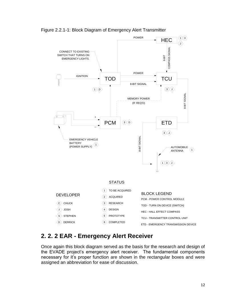
Figure 2.2.1-1: Block Diagram of Emergency Alert Transmitter
TCU
+
_
+_
EMERGENCY VEHICLE
BATTERY
(POWER SUPPLY)
8-BIT SIGNAL
HEC
MEMORY POWER
8-B
IT
CO
MP
AS
S S
IGN
AL
TOD
PCM
(IF REQ'D)
1
3
1 3
3
D
D
J
J
1
CONNECT TO EXISTING
SWITCH THAT TURNS ON
EMERGENCY LIGHTS.
POWER
POWER
IGNITION
BLOCK LEGEND
PCM - POWER CONTROL MODULE
TOD - TURN ON DEVICE (SWITCH)
HEC - HALL EFFECT COMPASS
TCU - TRANSMITTER CONTROL UNIT
ETD - EMERGENCY TRANSMISSION DEVICE
STATUS
1 TO BE ACQUIRED
ACQUIRED
RESEARCH
DESIGN
PROTOTYPE
COMPLETED
2
3
4
5
6
DEVELOPER
CHUCK
JOSH
STEPHEN
DERRICK
C
J
S
D
ETD
3 J
J1 3
8-B
IT S
IGN
AL
8-B
IT S
IGN
AL
AUTOMOBILE
ANTENNA 1
2. 2. 2 EAR - Emergency Alert Receiver
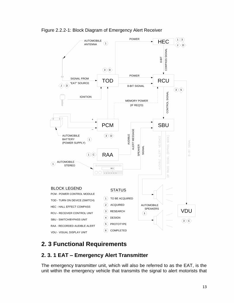
Once again this block diagram served as the basis for the research and design of the EVADE project‟s emergency alert receiver. The fundamental components necessary for it‟s proper function are shown in the rectangular boxes and were assigned an abbreviation for ease of discussion.
13
Figure 2.2.2-1: Block Diagram of Emergency Alert Receiver
RCU
+
_
+_
AUTOMOBILE
ANTENNA
AUTOMOBILE
BATTERY
(POWER SUPPLY)
SIGNAL FROM
"EAT" SOURCE8-BIT SIGNAL
HEC
MEMORY POWER
POWER
8-B
IT
CO
MP
AS
S S
IGN
AL
TOD
PCM
(IF REQ'D)
1
1
3
3
3
3
D
D
S
J D
1
J D
POWER
IGNITION
BLOCK LEGEND
PCM - POWER CONTROL MODULE
TOD - TURN ON DEVICE (SWITCH)
HEC - HALL EFFECT COMPASS
RCU - RECEIVER CONTROL UNIT
SBU - SWITCH/BYPASS UNIT
RAA - RECORDED AUDIBLE ALERT
VDU - VISUAL DISPLAY UNIT
1 2 3 4 5 6
96.5
SP
EA
KE
R
RAAAUTOMOBILE
STEREO
AUTOMOBILE
1
SPEAKERS
1
1
AU
DIB
LE
ALE
RT
ME
SS
AG
E
C SIG
NA
L
VDU
3 C
SBU
CO
NT
RO
L S
IGN
AL
STATUS
1 TO BE ACQUIRED
ACQUIRED
RESEARCH
DESIGN
PROTOTYPE
COMPLETED
2
3
4
5
6
2. 3 Functional Requirements
2. 3. 1 EAT – Emergency Alert Transmitter
The emergency transmitter unit, which will also be referred to as the EAT, is the unit within the emergency vehicle that transmits the signal to alert motorists that
14
the emergency vehicle is approaching. As can been observed from the block diagram created to show the general breakdown of the unit, the emergency alert transmitter requires a power control module, a turn on device module, a compass or GPS system, a control unit, and the actual transmitter antenna.
2. 3. 1. 1 PCM – Power Control Module
The power control module (PCM) provides the necessary power to operate the various components within the system. Because there are two distinct devices involved in the system design (the EAT and the EAR), each with slightly different components with different power needs, there must be two distinct PCMs with different design specifications. The PCMs will both receive power from an automotive battery/alternator setup and condition this power as needed. Different voltage levels are provided with sufficient current to drive all components simultaneously. Other factors, such as ripple, noise, and waste heat were considered.
2. 3. 1. 2 TOD – Turn On Device
The turn-on device (TOD) serves as the gatekeeper between the PCM and the components attached to it. It prevents power from being applied to components when the system is in a non-emergency state of operation, thus conserving power, reducing generation of waste heat, and extending the life of components. For the EAT, the TOD simply consists of the same switch used to operate the emergency vehicle lights. Thus, when the lights are activated, the EAT is automatically be activated as well.
2. 3. 1. 3 HEC/GPS – Hall Effect Compass / GPS
In order for the emergency alert device to alert the driver of the passenger vehicle about an approaching emergency vehicle, information must be gathered about where the emergency vehicle is in proximity to the passenger vehicle. This information needs to be the distance the emergency vehicle is from the passenger vehicle and the direction the two vehicles are traveling. Or, if one or both of them are not moving the direction that vehicle is facing is also needed information. In order to gather this needed information two different electronically controlled devices will be used in complimentary of each other, a GPS module and a Hall-effect compass. The Hall-effect compass is an electronic compass that uses the horizontal flux pattern of the earth‟s magnetic field to indicate the cardinal directions. Since this sensor uses the magnetic field, it works in any environment. When installed in both an emergency vehicle and a passenger vehicle, the Hall-effect compasses provide the necessary information to determine the heading of each vehicle, which is necessary to correctly identify possible alert situations.

15
The Hall-effect compass will need to be able to accurately measure not only the four cardinal directions ( N, E, S, W ) but, the four intermediate cardinal directions ( NE, NW, SE, SW ) as well. Often roads will tilt when going around sharp corners or up a steep mountain, so the compass will need to be able to still work when it is tilted. About a 10 to 12 degree of tilt should be the most degree of tilt that a road will make for any considerable distance. The power consumption of this device should be able to be handled by a typical vehicle. A typical vehicle operates at 12 volts, so a vehicle should have plenty of power to supply to a component like this. The GPS module is a global positioning system that can pinpoint the positions of the emergency vehicle and the passenger vehicles. Knowing the proximity the emergency vehicle is to the passenger vehicle is needed information to transmit to the passenger vehicle, so that the proper avoidance maneuvers can be taken if necessary.
2. 3. 1. 4 TCU – Transmitter Control Unit
The main function for the transmitter control unit is to gather the information from the Hall Effect Compass or GPS sensor and logically combine that information into the signal that is transmitted to the emergency alert receivers in the other vehicles. This system is essentially the brains of the emergency alert transmitter and is very important in determining how the transmitter and receivers will interact. The transmitter control unit is designed to not require much power so that it doesn‟t drain the battery of the vehicle. Since the unit takes the data from multiple devices and combines that data into one signal, we needed some sort of memory as well as the ability to implement some sort of logic.
2. 3. 1. 5 ETD – Emergency Transmission Device
The objective of the transmitter is to send information about the emergency vehicle from the emergency vehicle to any passengers‟ vehicle that is in a specified distance of the emergency vehicle. The information will only need to be sent when the emergency vehicle is in any emergency mode such as a police car in a pursuit of a stolen vehicle, an ambulance in route to a car accident, or a fire truck in route to a house fire. The information that will need to be sent from the emergency vehicle to the car is the type of emergency vehicle that is in the area and where the emergency vehicle is at in proximity to the passengers‟ vehicle, so the car can move out of the way or take any necessary precautions. The information that needs to be generated about the type of emergency vehicle that is generating the emergency signal can easily be done with a microprocessor. The information that needs to be generated about the proximity of the emergency vehicle to the passengers‟ vehicle will be done with a combination of a digital compass and a GPS module. The combination of the digital compass and GPS module will be able to detect the direction of the passengers‟ vehicle is facing even if the car is not moving. This would not be

16
possible with a GPS module alone. The information from the digital compass and the GPS module can be sent to the microprocessor, so the microprocessor will generate a binary form of the all the information that needs to be sent to the passengers‟ vehicle. In order for the transmitter to send the information about the emergency vehicle to the passengers‟ vehicle, the information will need to be in a form that can be easily transmitted from the emergency vehicle to the passengers‟ vehicle. A bit stream of the binary information can easily be generated with the microprocessor and this bit steam of information could then be transmitted to the receiver in the passengers‟ vehicle with a proper transmitter. The transmitter will need to be powerful enough to transmit the information in a suitable distance from the emergency vehicle so that the passengers‟ vehicle receiving the signal will have an ample amount of time to get out of the way or make proper avoidance maneuvers. Most construction signs start at about 1500 feet from the construction zone, so it is believed that this 1500 feet range is a proper awareness distance for pedestrian vehicles to make proper adjustments or evasion maneuvers. If the transmitter could transmit at about 1500 feet, then an emergency vehicle traveling at about 80 miles per hour would give the passengers‟ vehicle about 13 sec to react, if the passengers‟ vehicle was not moving. Depending on the direction of the passengers‟ vehicle to the direction of the emergency vehicle the time for the passengers‟ vehicle to react to the emergency vehicle will be a little less, if they were traveling towards each other, or a little more, if they were traveling away from each other. When the transmitter and receiver are operating in the real world, they will in counter many different environments to operate in. The different environments that the transmitter and receiver operate in will alter the performance of the system. If the system was in an area were the signal could not travel through its environment as well, the transmitter and receiver will not operate as expected. The downtown part of a big city with lots of sky-scraper is an example of an environment that the transmitter and receiver will not operate as well as expected too. So, the amplification of the transmitter should be sufficient enough to travel the expected distance, 1500 feet, that the system is expected to operate at, no matter the environment it is in. To combat this performance problem the transmitter should be made to operate at its expected performance level in the most extreme environment. Making the transmitter operate properly in the most extreme environment will make it operate better than expected in less extreme environments, such as a county road or highway that is open of any major obstacles that could block the signal. This is acceptable because it will only give the pedestrian in the vehicle more time to take proper avoidance maneuvers. So, the specs of the transmitter will need to meet two basic requirements. It will need to transmit the information at least 1500 feet, no matter what type of environment it is in, and be able to transmit a bit stream of binary information that

17
will tell the passengers‟ vehicle all the needed information about the emergency vehicle. Another important specification that the transmitter and receiver will need to meet is the proper frequency. The frequency that the transmitter and receiver operate at should be in the range that can be handled by the antenna of the vehicles. This will make this project require fewer components. With fewer components, the cost of this project will be lower.
2. 3. 2 EAR – Emergency Alert Receiver
The project is able to fit into a typical vehicle without anyone noticing that it is there unless it is sending a message. So any component of the car that could be used was used to make this project as unnoticeable as possible. The emergency alert receiver is able to use the antenna of the car to receive the signal from the transmitter in the emergency vehicle. This means that the receiver must operate at a frequency that the antenna can handle. The accuracy of the receiver is also a major issue. The information that is coming from the transmitter is binary information, so if the receiver does not accurately receive the information then it could give errors about the direction or the proximity of the vehicles. The output of the receiver is also at a sufficient voltage that can easily be handled by the receiver‟s control unit that dissects the information that is being sent to the motorists‟ vehicle.
2. 3. 2. 1 PCM – Power Control Module
The power control module for the emergency alert receiver will serve the exact same purpose as the power control module in the emergency alert transmitter, except that the receiver power control module will be responsible for supplying power to the various elements of the emergency alert receiver, which will require more consideration because of additional units like the visual display and the recorded audible alert system. For a more detailed description of the actual functionality of the power control module, see Section 2. 2. 1. 1 for the description given for the emergency alert transmitter.
2. 3. 2. 2 TOD – Turn On Device
The turn-on device (TOD) for the emergency alert receiver will serve the exact same purpose as the TOD in the emergency alert transmitter, though it will be quite a bit more complex. For the EAR, the TOD will need to sense the incoming signal and determine whether it is a genuine signal from an emergency vehicle or some other signal transmitted on the same carrier frequency. If the signal is confirmed to be an emergency vehicle signal, the TOD will then activate the rest of the EAR circuits. It will also need some sort of buffer so that the emergency vehicle signal can be retained while it is being verified. If verification is confirmed, then the signal will be passed to the receiver control unit. If the entire message is not present, then the message will be discarded and the EAR will not be activated.

18
2. 3. 2. 3 HEC/GPS – Hall Effect Compass/GPS
The Hall effect compass and global positioning system for the emergency alert receiver will be exactly the same as in the emergency alert transmitter, except that the signal to the receiver control unit will be compared with the transmitted signal in order to determine the orientation of the vehicles in relation to one another. For the more detailed description, see Section 2. 2. 1. 3.
2. 3. 2. 4 RCU – Receiver Control Unit
Similar to the function of the transmitter control unit, the receiver control unit also serves as the “brain” of the entire receiver system, performing all of the logic and sending out most of the commands. The receiver control unit must perform the even more complex function of not only gathering the same information about the location of the vehicle from the compass and the global positioning system, but also receiving and decoding the signal transmitted from the emergency vehicle. All of this information is combined within the calculations in order to determine if there is an approaching emergency vehicle and from what direction. Once this information is decoded, the receiver control unit has the additional task of sending the appropriate signals to the visual display unit and recorded audible alert so that the correct message is displayed for the driver to see. It is important that this unit is very power efficient so that it does not greatly drain the vehicle‟s battery by demanding a lot of power from the power control unit. It also has good temperature control because most logic units, such as processors, dissipate a lot of energy as heat; since this unit is enclosed in the dashboard of the vehicle in a small space, it is important that the unit have good temperature control so that it does not cause overheating, which shortens the lifespan of the design and possibly creates a fire hazard.
2. 3. 2. 5 SBU – Switching Bypass Unit
When an emergency vehicle approaches a passenger vehicle with an installed emergency alert receiver unit, a pre-recorded alert message will be triggered and played from the recordable audible alert module (RAA). In order to reduce cost, to save space, and to prevent the passenger vehicle‟s stereo from drowning out the alert message, the emergency alert receiver will utilize the vehicle‟s own speakers rather than integrating separate speakers into the system‟s design. The only two methods for using the vehicle‟s speakers are 1) to tap into the auxiliary input in the car‟s stereo or 2) to tap into the speaker lines and bypass the stereo signals. Since some stereo units do not have an auxiliary input jack and others may be using that jack for other inputs (like satellite radio), the emergency alert receiver will tap into the vehicle‟s speaker lines directly and bypass the stereo signals when necessary. This will also allow the system to function properly when the vehicle‟s stereo is off, as the system will have its own power supply. Because car stereos amplify their signals before sending them to the speakers, the output from the recordable audible alert will also need to incorporate one or more signal amplifiers in order to properly drive the speakers.

19
Accomplishing these tasks will be the purpose of the switching bypass unit (SBU).
2. 3. 2. 6 RAA – Recorded Audible Alert
The Recoded Audible Alert (RAA) device will contain several pre-recorded messages in both English and Spanish that will alert the driver of a passenger vehicle of to an oncoming emergency vehicle. The RAA will utilize information gathered from both the Hall-effect compass (HEC) module and the GPS module to determine the pre-recorded message to play. For example, when the passenger vehicle is travelling northbound, and the emergency vehicle is travelling northbound, and the vector distance between the two vehicles is getting smaller, this will require the RAA to play the message, “Emergency vehicle approaching from rear.” Conversely, if the passenger vehicle is travelling southbound, and the emergency vehicle is travelling northbound, the RAA will play the message, “Emergency vehicle approaching from front.” Once the proper signal is obtained, and the particular message is ready to play, the RAA will transmit the proper message to the Switch/Bypass Unit (SBU) which will bypass the radio transmission, amplify the RAA message, and send the message to the passenger vehicle speakers. A selectable language button may be incorporated into the design to toggle which language is used to transmit the recorded message. The message should repeat every 10 seconds until the emergency vehicle has passed the passenger vehicle. After the emergency vehicle has passed the passenger vehicle, the vector distance between the two vehicles will begin to increase. At this time, the RAA will stop transmitting any messages, and the SBU will allow the radio transmission to resume. In the event that the passenger vehicle is approaching an emergency vehicle, such as when an accident is in the path of the passenger vehicle, and the emergency vehicle is transmitting a signal, the vector distance between the two vehicles will be getting smaller, and the RAA will transmit, “Approaching emergency vehicle ahead.” This scenario should only occur when “ahead” is one of the three forward compass points relative to the passenger vehicle. For example, if the passenger vehicle is travelling northbound, and the emergency vehicle is stopped ahead of the passenger vehicle in either north, northeast, or northwest position, it would be appropriate to transit this message. Similarly, when the passenger vehicle is headed eastbound, and the emergency vehicle is stopped east, northeast, or southeast, the same message will play.
2. 3. 2. 7 VDU – Visual Display Unit
The Visual Display Unit will alert the driver that an emergency vehicle is approaching in two ways. First, an LCD screen will display a preprogrammed message onto the screen. This message will alert “Emergency Vehicle Approaching” and add a fourth line “from front”, “from rear”, “from left”, or “from

20
right”. This will allow a hearing impaired driver to realize an emergency vehicle is approaching, and from which direction the emergency is coming towards them. Second, a flashing LED, around the bezel of the LCD screen, will draw attention to the message appearing on the screen, as well as the direction of the emergency vehicle. The completed design will have an array of LED‟s that refer to the eight basic directions transmitted by the hall-effect compass (N, S, E, W, NE, NW, SE, SW). As the emergency vehicle approaches, and then passes, the LED array should follow the direction of the emergency vehicle. Under normal operation, the display will show “Heading “ (direction) since we will have a hall-effect compass in the passenger vehicle Emergency Alert Receiver, and the LED lights will be turned off. The 16x4 LCD screen is laid out to allow 16 characters across per row, with four rows down as shown in Figure 2.3.2.7-1. Here is an example of what will be displayed on the screen under normal operation: Figure 2.3.2.7-1: Normal Compass Display for North
Taking advantage of the compass keeps the display from being blank during times when no emergency vehicles are approaching. The Hall-effect compass can detect eight directions, each of which needs to be displayed on the screen as shown in Figure 2.3.27-2. Keeping this in mind, the character set for each of the directional headings will be as follows:
Figure 2.3.2.7-2: Northeast and Northwest Compass Headings
This is the other two Northern direction messages and character placement. The Southern directions in Figure 2.3.2.7-3 are shown as they should be displayed.

21
Figure 2.3.2.7-3: South, Southeast, and Southwest Compass Headings
Finally, the character placement for East and West are shown in Figure 2.3.2.7-4 and follow the exact same formatting as the previous letters. These displays shall be as follows:
Figure 2.3.2.7-4: East and West Compass Headings
During programming of the LCD screen, it is important to denote the precise location for each character displayed to the screen. Incorrect placement of the characters could result in each character overwriting the previous as they are displayed to the screen.
The primary function of the VDU is to visually alert the driver when an emergency vehicle is approaching, and alert the driver as to the direction the emergency vehicle is traveling with respect to the passenger vehicle. For this process, we will take advantage of the GPS module in both the transmitter and receiver, as well as the hall-effect compass in both units. First, to discuss the LCD module, the reason for the 16x4 display size is to accommodate the message “EMERGENCY VEHICLE APPROACHING FROM RIGHT” as shown in Figure 2.3.2.7-5. The character placement for this message is as follows:
Figure 2.3.2.7-5: Alert Message for Vehicle on Right
“RIGHT” denotes any logical negative angle from -46 degrees to -134 degrees of the emergency compass in relation to the passenger compass.

22
“APPROACHING” denotes the coordinates computed from the two GPS modules whereas the difference of the vector between the latitudes and between the longitudes is getting smaller. This will be discussed in more detail in the design section of this document. Figure 2.3.2.7-6: Alert Messages for Left, Rear, and Front
Again, similar formula functions shall be used to determine the correct message to be displayed. The LED lights will surround the LCD screen along the bezel as illustrated in Figure 2.3.2.7-7. The bezel will serve as the protective cover to the internal components, as well as the mounting device to the vehicle dashboard. In general, it should look as follows:
Figure 2.3.2.7-7: LCD Display Bezel
LED 1
LED 2
LED 3
LED 4
LED 5
LED 6
LED 7
LED 8
23
3. Research
3. 1 Research Methodology
The vast amount of time invested in the EVADE project during Senior Design I had been dedicated to research every detail of the project and every possible method of implementing the requirements for the design. Before research was started, the EVADE group met and the research and design topics were delegated based largely on the interests and experience of each individual. Careful consideration was put into the extent of research necessary for each element in order to avoid overloading one member with too much research and therefore burdening that person unfairly and risking the delay of the project design. This also ensured that every member was able and expected to contribute equally to the development of the EVADE project, most notably at this point the documentation.
The majority of the research for the EVADE project was performed through the use of internet search engines to discover published documentation, parts manufacturers and venders, previous design projects, and other helpful material such as programming forums and electronic hobbyist guides. Previous textbooks, notes, and laboratory experiments from past courses such as signals and systems, electronics, and embedded systems were also consulted in order to gain a better feel for previous exposure to material that might be relevant. Finally, we consulted fellow class-mates, co-workers, and professors who might have previous experience with specific hardware and venders in order to tap into the vast resources of knowledge they would have available.
The majority of the research was invested in exploring all of the different options available for use. Once these options were explored, the group sat down and decided on which specific options to use in the integration of the various elements. From that point, the research switched to determining the specific parts to be used in the project; this was mostly done by reviewing data sheets and determining which parts not only performed their functions the best, but also which parts were the best for total integration, since the cheapest and best control unit may not integrate with the GPS sensor in the most efficient way. All of these considerations we researched so that the design could focus mostly on the final integration of parts and developing schematics for the prototype.
The following sections are devoted to discussing the ideas researched and proposed for the different components of the design. Each component will generally be discussed separately except for cases where we discovered that we could combine components for simpler and cheaper implementation. Each section will discuss the various technologies available to implement the specifications for that component, including an analysis of the pros and cons of each possible method for implementation.

24
Once each of the possible options for implementing the design were reviewed, we will discussed which method to choose for the prototyping and why we chose that option based on such factors as cost, ease of implementation, size, quality, and compatibility with the other components.
3. 2 EAT – Emergency Alert Transmitter
The emergency transmitter unit, which will also be referred to as the EAT, is the unit within the emergency vehicle that will transmit the signal to alert motorists that the emergency vehicle is approaching. As can been observed from the block diagram created to show the general breakdown of the unit, the emergency alert transmitter will require a power control module, a turn on device module, a compass or GPS system, a control unit, and the actual transmitter antenna. Each of the components were assigned to different members of the group for research and design, which will be discussed in detail for each of the individual units, including the possible options researched and the final selection of parts.
3. 2. 1 PCM – Power Control Module
The purpose of the power control module is to provide specific voltage levels required by the various system components. The input to the module is the 12 V line from the automotive battery/alternator. The required outputs from the PCM are 3V and 5V. While providing the different output voltages, the power control module must also stabilize those voltages against variations, both induced from the alternator input and from changes in the load conditions.
3. 2. 1. 1 Simple Resistive Voltage Divider Topology
The simplest scheme for realizing the PCM is a simple voltage divider circuit implemented with only series resistors. The various voltage levels are determined by the ratios of the individual resistors to the total circuit resistance. The major drawback to this setup is that it is very susceptible to loading effects. As loads are connected to the output(s), the impedance of the branches changes dramatically, causing fluctuations in the voltage levels. To guard against such fluctuations, the impedance of the loads should be quite high compared to that of the circuit resistors. However, high load impedance causes most of the power developed by the battery to be wasted as heat dissipated through the resistors.
3. 2. 1. 2 Shunt Regulator Topology
The resistive voltage divider may be modified to include one or more Zener diodes to stabilize the output of the shunt regulator circuit. An example of this type of power supplying network is shown in Figure 3.2.1-1 below. Each Zener diode is designed with a specific breakdown voltage. While operating within the breakdown region, the diode maintains this voltage over a wide range of
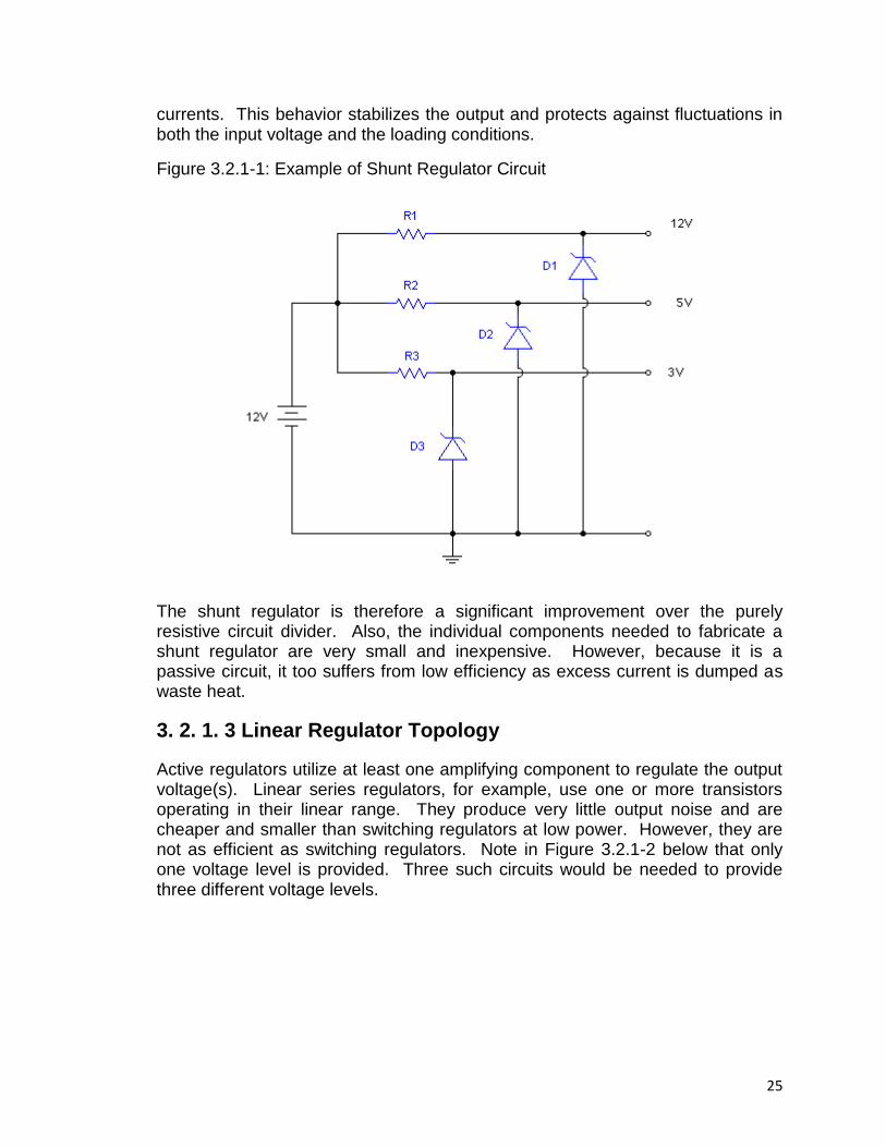
25
currents. This behavior stabilizes the output and protects against fluctuations in both the input voltage and the loading conditions.
Figure 3.2.1-1: Example of Shunt Regulator Circuit
The shunt regulator is therefore a significant improvement over the purely resistive circuit divider. Also, the individual components needed to fabricate a shunt regulator are very small and inexpensive. However, because it is a passive circuit, it too suffers from low efficiency as excess current is dumped as waste heat.
3. 2. 1. 3 Linear Regulator Topology
Active regulators utilize at least one amplifying component to regulate the output voltage(s). Linear series regulators, for example, use one or more transistors operating in their linear range. They produce very little output noise and are cheaper and smaller than switching regulators at low power. However, they are not as efficient as switching regulators. Note in Figure 3.2.1-2 below that only one voltage level is provided. Three such circuits would be needed to provide three different voltage levels.

26
Figure 3.2.1-2: Example of Active Regulating Circuit Design
3. 2. 1. 4 Switching Regulator Topology
Switching regulators, such as DC to DC converters, operate by alternately storing and discharging energy to maintain stable voltage outputs. An inductor and a capacitor control the current through the regulator circuit while a transistor acts as a switch, controlling the duty cycle. When the switch is closed, the transistor is nearly fully conducting and therefore dissipates very little waste heat. At the same time, energy is being stored in the inductor and capacitor while the Zener diode maintains a steady output voltage. When the switch opens, no power is drawn from the battery; instead, the storage elements release their stored energy to maintain a constant output voltage. This allows the switching regulator to attain relatively high efficiency. Also, at higher power output (above a few watts), the switching regulator is cheaper than the linear series regulator because less waste heat is generated and heat management components can be smaller. As above, the circuit diagram shown in Figure 3.2.1-3 below shows only one output voltage. Several similar circuits would be needed to fully realize the PCM.
Figure 3.2.1-3: Example of Switching Regulator Circuit
3. 2. 1. 5 Topology Evaluation and Design Criteria
All of the above realizations for the power control module are able to provide the necessary voltage levels for the various components of the emergency alert

27
system, and all except the resistive voltage divider have some sort of voltage stabilization built into them as well. The most important differences between the realizations are in output noise, efficiency, cost, and size. Because the PCM will be supplying power to a radio frequency (RF) transmitter and receiver, it is critical that the noise content of the output lines is minimized, especially noise near the transmission frequency. Switching regulators typically operate at high switching frequencies, and are therefore notorious for introducing radio frequency interference (RFI) into their outputs. For this reason, switching regulators are a poor choice for the PCMs. Both the emergency alert transmitter (EAT) and the emergency alert receiver (EAR) may be operated for relatively long periods, perhaps for several hours of continuous use. So after output noise, efficiency and heat dissipation are of the next greatest importance in selecting a regulator circuit. For this reason, neither the resistive series voltage divider nor the shunt regulator is a suitable candidate for the PCMs. Size is also a consideration since the devices are intended to be mounted inside a vehicle‟s dashboard. However, if necessary, the system can be installed in the trunk, so size is not going to be a deciding factor. Considering all factors, the most suitable component for the PCM is the active linear regulator. Linear regulators are less efficient than switching regulators, but they provide very clean outputs. Linear regulators are more expensive than passive regulators, but are far more efficient. The efficiency advantages, as well as the simplicity of surface mounting far outweigh the moderate cost savings of passive regulators.
3. 2. 2 HEC/GPS – Hall Effect Compass / GPS
Choosing the right GPS module and electronic Hall-effect compass was very important in the design of this project. Choosing a component that has more features than what is needed would have raised the total cost of the device, and a major part of engineering is to keep costs as low as possible. On the other hand, choosing a component that does not have the proper features for this application would have made the device not operate as expected. Once all the features of each component were known then different features could be integrated into the project to give applications that were not originally thought of in the beginning.
3. 2. 2. 1 Hall Effect Compass
After researching the different types of electronic Hall-effect compasses it was found that only The Robson Company, Inc. was the only maker of this type of electronic compass using Hall-effect sensors because they have control of the patent. The patent was established on Aug 31, 1993 by Kim Kwee Ng and the patent number is 5241270. Now that it is known what company is going to supply the electronic Hall-effect compass, deciding which compass to use is the next step because they supply multiple types of this compass. The different electronic Hall-effect compasses that The Robson Company supplies are the Digital Sensor
28
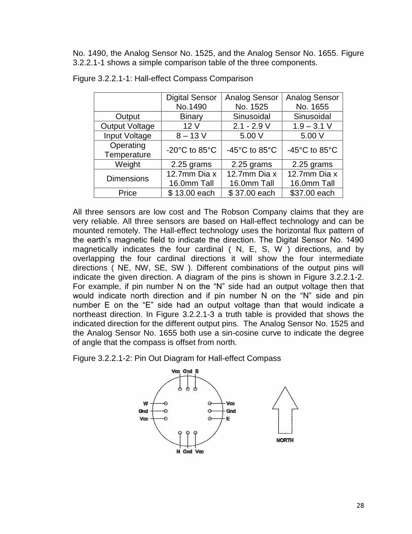
No. 1490, the Analog Sensor No. 1525, and the Analog Sensor No. 1655. Figure 3.2.2.1-1 shows a simple comparison table of the three components.
Figure 3.2.2.1-1: Hall-effect Compass Comparison
Digital Sensor
No.1490 Analog Sensor
No. 1525 Analog Sensor
No. 1655
Output Binary Sinusoidal Sinusoidal
Output Voltage 12 V 2.1 - 2.9 V 1.9 – 3.1 V
Input Voltage 8 – 13 V 5.00 V 5.00 V
Operating Temperature
-20°C to 85°C -45°C to 85°C -45°C to 85°C
Weight 2.25 grams 2.25 grams 2.25 grams
Dimensions 12.7mm Dia x 16.0mm Tall
12.7mm Dia x 16.0mm Tall
12.7mm Dia x 16.0mm Tall
Price $ 13.00 each $ 37.00 each $37.00 each
All three sensors are low cost and The Robson Company claims that they are very reliable. All three sensors are based on Hall-effect technology and can be mounted remotely. The Hall-effect technology uses the horizontal flux pattern of the earth‟s magnetic field to indicate the direction. The Digital Sensor No. 1490 magnetically indicates the four cardinal ( N, E, S, W ) directions, and by overlapping the four cardinal directions it will show the four intermediate directions ( NE, NW, SE, SW ). Different combinations of the output pins will indicate the given direction. A diagram of the pins is shown in Figure 3.2.2.1-2. For example, if pin number N on the “N” side had an output voltage then that would indicate north direction and if pin number N on the “N” side and pin number E on the “E” side had an output voltage than that would indicate a northeast direction. In Figure 3.2.2.1-3 a truth table is provided that shows the indicated direction for the different output pins. The Analog Sensor No. 1525 and the Analog Sensor No. 1655 both use a sin-cosine curve to indicate the degree of angle that the compass is offset from north.
Figure 3.2.2.1-2: Pin Out Diagram for Hall-effect Compass

29
Figure 3.2.2.1-3: Truth Table for Hall-effect Output
Output Direction
N S E
W
NE NW SE SW
Output Pin N
1 0 0 0 1 1 0 0
Output Pin S
0 1 0 0 0 0 1 1
Output Pin E
0 0 1 0 1 0 1 0
Output Pin W
0 0 0 1 0 1 0 1
From the comparison table it can be seen that the two analog compasses are actually comparable in many ways, but the digital compass differs a lot. The output voltages of the analog compasses are the only thing that differs from the two, so the Analog Sensor No. 1655 is just an upgrade of the Analog Sensor No. 1525. The datasheet of the two analog compasses explains that the input voltage of 5.00 volts had to be closely regulated or the devices would not operate as expected, so this would be a downfall for using ether one of these components. On the other hand, the input voltage of the binary compass has a range of 8 to 13 volts which makes it easy to integrate into the project. Another downfall for the two analog compasses is that the price is almost triple that of the binary one, and keeping costs as low as possible is a major part of engineering. The operating temperature of the two analog compasses has a wider range that that of the binary compass, but the range of the analog compass just allows it to be used in extremely cold climates. These extremely cold climates should not be an issue for the project because the components are inside the dash of the vehicle. The weight of all three of the compasses is low for all three, so this will not be an issue. Also, the dimensions of all three of the compasses are the same and small enough to fit on any printed circuit board.
Each one of the compasses has roughly a twelve degree angle of allowable tilt before they may start to give errors in the output. While for most roads this will not be a problem, but some steep hills in some inner cities (such as San Francisco) this may become a problem. In the testing it will be needed to test the errors that come up when a vehicle is tilted beyond twelve degrees. Each one of the sensors has a damper that gives the same speed indication as a liquid filled compass, that is, 0.5 second response from 90° displacement without over swing. This damper is to keep the compass from having a flutter affect when turning to fast.
After reviewing the three possible compasses to use for this project it has been decided to use the Binary Sensor No. 1490. Since the control unit is better suited to accept a binary signal, using a binary compass makes sense. If one of the analog compasses was used then an analog to digital converter would have to

30
be used and that would add more components to the project. More components would make the cost of the project more and that is a downfall. The output voltage of the binary compass is the only undesirable characteristic of the compass, but lowering the voltage for the control unit can be done with resistors or an attenuator.
After testing the Robson Binary Sensor No. 1490, we found that it did not give the accuracy that was desired for the application in our project. So, a different type of digital compass was researched after that, the Honeywell HMC 6352. This is a digital compass module that combines 20axis magneto-resistive sensors. The HMC6352 communicates with a microprocessor through an I2C protocol. The compass outputs data in three different modes. Heading Mode, the one we are using in this project, outputs the heading in a binary number from 0 to 3599. This number represents the compass heading in one tenth of a degree from north (0°). The other two modes output the raw X and Y magnetometer data from the internal sensor values measured by the compass module. The only difference between the two is that one mode offers an offset, so true north can be established. Figure 3.2.2.1-4 shows the Power and Environmental characteristics of the HMC 6352.
Figure 3.2.2.1-4: Power and Environmental characteristics
HMC6352 Min Max
Supply Voltage 2.7 V 5.2 V
Supply Current 1 mA 10 mA
Heading Accuracy 2.5 degRMS
MAX. Exposed Field 10k gauss
Operating Temperature -20°C 70°C
Storage Temperature -55°C 125°C
Size 6.5 x 6.5 x 1.5mm
Weight 0.14 grams
3. 2. 2. 2 Global Positioning Sensor
Researching the GPS modules was a little bit more challenging than researching the Hall-effect compass. Since there was only one manufacturer of Hall-effect compasses, there are only a few choices to choose from. This was not the case with the GPS module. There are many different manufacturers of GPS modules, so choosing the proper one for this application required more research and thought. After reading about different types of GPS modules it was decided to choose one of the following: the GlobalSat EM-408, the Modulstek MG-S01SP, or the Antenova M10214-A1. It was decided to base the decision on four characteristic areas of the three GPS modules. The four characteristic areas are shown in the general characteristics Figure 3.2.2.2-1, performance characteristics Figure 3.2.2.1-2, power supply Figure 3.2.2.2-3, and environmental specifications Figure 3.2.2.2-4.

31
Figure 3.2.2.2-1: Comparison of GPS General Characteristics
General Characteristics
GlobalSat EM-408
Modulstek MG-S01SP
Antenova M10214-A1
Receiver Architecture
20 channels 1 satellite /
channel L1 1575.42 MHz 1.023 MHz chip
rate
20 channels 1 satellite /
channel L1 1575.42 MHz 1.023 MHz chip
rate
20 channels 1 satellite /
channel L1 1575.42 MHz 1.023 MHz chip
rate
Antenna Built-in or external Built-in Built-in
Data Output Protocol
SiRF Binary NMEA 0183
NMEA 0183 SiRF Binary NMEA 0183
Dimensions 36.4 x 35.4 x
5mm with antenna
19 x 19 x 6.5mm with antenna
43 x 9 x 4mm with antenna
Cost $49.00 each $54.00 each $ 49.75 each
The receiver architecture for each GPS module is the same for all three, so this will not help with the decision of which one to use for this project. The 20 channels with 1 satellite / channel will allow great performance for the application of this project. The more satellites that the GPS module can connect to at once will help with the accuracy of the GPS module. The L1 1575.42 MHz is the frequency that currently contains the coarse acquisition signal used by all civilian GPS users. Implementation will provide a course acquisition code to ensure backward compatibility, and assure a 1.5 dB increase in minimum course acquisition code power to moderate any increase in the noise floor. The 1.023 MHz chip rate will allow fast processing. Both the Modulstek MG-S01SP and the Antenova M10214-A1 have built in antennas, while the GlobalSat EM-408 has a built in and external antenna. Each one of the modules uses different processors, but the performance of each of the processors is comparable. So, this will not affect the decision of which module to use for this project. The data output protocol is an important part of this project. This is some of the information that needs to be sent from the emergency vehicle to the motorists‟ vehicle. Since both the Antenova M10214-A1 and the GlobalSat EM-408 both use SiRF Binary or NMEA 1083 data output protocol, it will not be a deciding factor in choosing the GPS module for this project. But, the Modulstek MG-S01SP only uses NMEA 1083 data output protocol. So, more research about what type of protocol the control unit can process easier will need to be done. Also, whatever protocol will be easier for the transmitter to handle will need to be researched more too. The dimensions of the three modules do differ, but the space that we have available in each vehicle to design each printed circuit board is plenty sufficient for any three of these modules.
32
Figure 3.2.2.2-2: Comparison of GPS Performance
Performance Characteristics
GlobalSat EM-408
Modulstek MG-S01SP
Antenova M10214-A1
Position Accuracy
3 m
7 m WASS corrected
1-5 m DGPS corrected
2.5 m
Cold Start Acquisition Rate
< 35 s 45 s average < 35 s
Hot Start Acquisition Rate
< 1 s 6 s average < 1 s
Tracking Mode Sensitivity
-159 dB -159 dB -159 dB
The performance characteristics for all three of the GPS modules are very similar. The position accuracy of any three of three modules will work well in the application of this project. The acquisition rate will not matter for the application of this project because the GPS module will be put in tracking mode when the vehicle starts up. So, the GPS module will have a fix on its position the entire time the vehicle is in motion. The tracking mode is the same for each one of the GPS modules, so this will also not be a deciding factor in choosing the proper GPS module.
Since the GPS module requires the power control module to supply any necessary power from the vehicle‟s battery, it is important that we consider the necessary power supply characteristics of each unit; these characteristics are considered in Figure 3.2.2.2-3.
Figure 3.2.2.2-3: Comparison of GPS Electrical Requirements
Power Supply
GlobalSat EM-408
Modulstek MG-S01SP
Antenova M10214-A1
Main Power Input, VCC
3.3 – 5.5 V DC 3.3 V DC 3.3 – 5.5 V DC
Main Supply Current
Acquiring < 55 mA Tracking < 35 mA Hibernate < 60 µA
40 mA Acquiring 50 mA Tracking 33 mA Hibernate 30 µA
Backup Power
0.3 – 5.5 V DC 3.3 V DC N/A
From this power supply chart it can be seen that once again each one of the GPS modules are very similar in their power supply. In the application of one of these devices in the project, a vehicle could easily supply the needed main power input, main supply current, and backup power. So, in terms of power supply any of these GPS modules with work fine in the project.

33
Figure 3.2.2.2-4: Comparison of GPS Environmental Requirements
Environmental Specifications
GlobalSat EM-408
Modulstek MG-S01SP
Antenova M10214-A1
Operating Temperature
-40°C to 85°C -10°C to 60°C -20°C to 85°C
Storage Temperature
-55°C to 100°C -20°C to 85°C -40°C to 85°C
Relative Humidity
5% to 95% non-condensing
5% to 95% non-condensing
5% to 95% non-
condensing
Altitude 18,000 m max 18,000 m max 18,000 m max
Velocity 545 m/s max 515 m/s max 545 m/s max
Acceleration 4 g max 4 g max 4 g max
In the environmental specifications the only component that raises an issue in this project is the Modulstek MG-S01SP because this operating temperature probably will not work in the application. The maximum operating temperature is 60°C and since the device will be install in the dash of a vehicle this operating temperature probably will not be high enough in the application of the project. The other two GPS modules have a maximum operating temperature of 85°C which should be sufficient for the application of the project. The storage temperature of the three modules will not raise any issue in the application of the component because it is not likely that a vehicle will be in an environment that gets below -20°C or above 85°C when the vehicle is parked somewhere. The relative humidity does not raise any concerns, even in Florida the humidity does not get above 95%. The altitude and velocity is definitely not an issue since a motorized vehicle will never be operating above 18,000 m or at 515 m/s. The acceleration will also not be an issue. Police vehicles will have a high acceleration rate when they in a high speed chase, but they will not exceed 4 g of acceleration.
Taking all things into consideration the general characteristics, the performance characteristics, power supply, and the environmental specifications it is believed that the Antenova M10214-A1or the GlobalSat EM-408 is the best GPS module for the application of this project. The cost of either of these components is in a desirable range and the data output protocol can be used in both of the SiRF Binary or the NMEA 1083 form. The fact that the GlobalSat EM-408 has an external will give us the option to add an external antenna if one is needed after testing. This along with all the other aspects of the component makes it the proper chose for the application of this project.
3. 2. 3 TCU – Transmitter Control Unit
The main function for the transmitter control unit is to gather the information from the Hall Effect Compass and GPS sensor and logically combine that information into the signal that is transmitted to the emergency alert receivers in the other

34
vehicles. This system is essentially the brains of the emergency alert transmitter and is essential in determining how the transmitter and receivers will interact. It is also important that this unit does not require much power so that it doesn‟t drain the battery of the vehicle. Since we needed a unit that is able to take the signals from multiple devices and combine them into one signal, we needed some sort of memory as well as the ability to implement some sort of logic.
The input protocols supported by the transmitter control unit were the largest design considerations in order to allow for the most flexibility in communication protocols during the research phase. The final compass module used I2C protocol to transmit the compass heading as a number between 0 and 3599. The GPS unit outputs a UART signal containing the information from the unit in the standard GPS formatting, spitting out information ranging from the number of satellites connected to the universal time to the latitude and longitude reading. Therefore the control unit accepts a UART signal and processes the special GPS signal, separating the necessary latitude and longitude from the additional information. Finally, the control unit has the ability to output all of this information in one bit stream as a UART signal that is transmitted and decoded by the receiver. Considering these requirements, the obvious choices for research were an FPGA or microcontroller, however, in order to be comprehensive in our research, a custom combination of logic chips and registers was researched as well.
3. 2. 3. 1 FPGA – Field Programmable Gate Array
An FPGA, or Field Programmable Gate Array, is a programmable logic device comprised of multiple individual logic „blocks‟ which can be programmed to perform one logical function. Once each block is assigned a certain logical function by the programmer, the blocks can be concatenated in order to form the desired string of logic. This design was created to be more flexible than the previous methods of creating a custom logic board comprised of individual standard logic components or the expensive application-specific option of a custom integrated circuit. As evidenced by the name “field programmable”, an FPGA is not a manufacturer-programmed device; rather, it is made to be programmed by the user for the user specific application. This means that the unit is able to perform many more functions than the user may need to implement and therefore care must be taken when selecting the type of FPGA needed so that the elements purchased are used as closely to their full potential as possible in order to reduce cost. While the use of each logic block to its full potential sounds like a daunting task, this is controlled mostly by the programming software that accompanies the FPGA and so therefore the effort involved is reduced simply to learning the programming language for the FPGA instead of any intricate wiring.
After researching popular FPGA‟s used in applications similar to ours, it became apparent that there were three dominant brands that were capable of offering the functionality that we needed at a reasonable price within the estimated budget:

35
XILINX, Altera, and Atmel. Once we determined the manufacturer, we researched more in order to narrow down the model of FPGA that would offer the functionality that we desired without containing too many features and thus bumping the FPGA out of the price range. After considering the number of inputs and outputs necessary, memory space needed, programming software included, power requirements, and temperature requirements, we narrowed our research possibilities to XILINX‟s Spartan 6, Altera‟s Cyclone II, or Atmel‟s AT40KAL.
XILINX’s SPARTAN 6
XILINX offers multiple different models of FPGA‟s varying from high performance, industry standard modules to lower cost, mid-range FPGA‟s to beginner pre-interfaced kits. The application did not require the intensive requirements of the industry standard FPGA‟s, especially since they are well outside of the budget we considered. On the other hand, we would waste numerous inputs and capabilities with the pre-interfaced modules. Therefore, we decided that the lower cost, low power Spartan 6 module had the potential to meet all of the requirements at an affordable price.
The first and most important requirement we considered was the number of inputs and outputs available as well as the capability to handle the types of inputs we needed. The Spartan 6 has the capability to handle over 40 different input and output standards, as well as up to 8 low power serial transceivers. The Spartan 6 is available with up to 576 usable user inputs and outputs, multiple 9 Kbit memory blocks and up to 147,443 logical elements. All of these logical elements, inputs and outputs, and memory can be directly controlled and programmed using XILINX‟s powerful ISE Design studio software with the added bonus of SelectIO advanced input/output configuration software.
As for the physical qualities that the FPGA must meet, XILINX‟s SPARTAN 6 seemed to have many of the same features as the other makes and models that we evaluated. The allowed operating temperature range given for the SPARTAN
6 on the datasheet was 0C ~ 85C, which seems reasonable for the expected operating conditions when the module is embedded in the dashboard of a vehicle. The input power necessary to operate the SPARTAN 6 is 3.3 V DC, which is easily within the range of the power control module. The largest sized package for the SPARTAN 6 is 31x31 mm, which is slightly smaller than the rest of the compared FPGA‟s. All of these characteristics are compared in Figure 3.2.3.1-1 with the characteristics of the other FPGAs.
Altera Cyclone II
Another very popular choice of FPGA for applications similar to ours was the Altera Cyclone II. While Altera manufactures multiple other models, the other models had more application specific features that made them more expensive without allowing the necessary utilization for the features of the project. Once again the most important consideration during research for the Cyclone II was
36
the number and types of inputs/outputs supported. According to the documentation on Altera‟s website, the Cyclone II features up to 622 usable input/output pins and up to 68,416 logic elements. The Cyclone II also features up to 1.1 Mbits of embedded memory. All of the logical elements, inputs and outputs, and embedded characteristics can be easily programmed and configured using the free Quartus II design software, which features HDL and schematic design entry for device programming.
When considering physical features such as power, size, weight, and temperature characteristics, the Cyclone II had very standard features when compared to other FPGAs. The general operating temperature requirements for
the Cyclone II are 0C ~ 85C, which was within the general temperatures that are expected within the dashboard of the average vehicle. The Cyclone II requires 1.2 VDC to power the core module and 3.3 VDC for the input/output module, which fits easily within the realm of what the power control unit can supply. The largest size for the Cyclone II package is 34.6x34.6 mm, weighing 11.6 g. These features are summarized in the FPGA comparison chart in Figure 3.2.3.1-1.
Atmel AT40KAL
The final FPGA that was researched and considered was Atmel‟s AT40KAL, which is Atmel‟s low cost, low power FPGA that is comparable to XILINX‟s SPARTAN 6 and Altera‟s Cyclone II. According to the data sheet available on Atmel‟s website, the Atmel AT40KAL features up to 384 input/output pins and up to 50,000 logical elements and up to 18,432 bits of RAM. In order to configure all of the inputs, outputs, logical elements, and memory, the AT40KAL features seamless integration with industry standard design tools such as Everest, Exemplar™, Mentor®, OrCAD®, Synopsys®, Verilog®, Viewlogic®, and Synplicity®.
The physical features of the AT40KAL are again very similar to all of the other FPGAs of similar capability. The general operating temperature requirements for
the AT40KAL are 0C ~ 70C for a commercial grade package or -40C ~ 85C for the more expensive industrial package; both of these temperature requirements should be within the general temperatures that can be expected within the dashboard of the average vehicle. The AT40KAL requires 3.3 VDC in order to fully power the FPGA, which fits easily within the realm of what the power control unit can supply. The largest size for the various AT40KAL packages is once again 34.6x34.6 mm. All of these characteristics are once again listed in Figure 3.2.3.1-1 in order to compare the three FPGAs side-by-side.
37
Figure 3.2.3.1-1: FPGA Characteristic Table
Characteristic: XILINX‟s SPARTAN 6
Altera‟s Cyclone II
Atmel‟s AT40KAL
Logical Elements
Up to 147,443 Up to 68,416 Up to 50,000
User I/O Up to 576 Up to 622 Up to 384
Memory 18 Kbits 1.1 Mbits 18,432 bits
Design Software
ISE Design Studio Quartus II Various (not included)
Operating Temperature
0C ~ 85C 0C ~ 85C 0C ~ 70C
Supply Power 3.3 V DC 3.3 V DC 3.3 V DC
Package Size 31 x 31 mm 34.6 x 34.6 mm 34.6 x 34.6 mm
Price Per FPGA
$25.20
(232 I/O, 14,579 logical elements)
$25.85
(182 I/O, 8256 logical elements)
$50.70
(193 I/O, 2304 logical elements)
3. 2. 3. 2 Microcontroller
A microcontroller is a small computer on a single integrated circuit fundamentally consisting of a simple processor, an internal clock, input and output ports, and limited memory. Microcontrollers are designed primarily for small, application specific tasks since they lack the memory space and processing power of a personal computer and function primarily based on the user specified programming using the software that is provided with the microcontroller. In this way a microcontroller is very similar to a FPGA in that it functions based on the programming controlled by the user and not the manufacturer. Since microcontrollers contain small processing units and memory created using integrated circuits, they are very fast and very diverse in their applications, as well as cheaper in comparison to FPGAs. They are also faster (on average) and are able to process multiple signals because of the built in support for all of the common communication protocols. Therefore, the key to determining that a microcontroller was more suitable than a FPGA rested mainly on cost, speed, and support information after considering all memory and input and output requirements. In the research of microcontrollers, the group considered two common types of microcontrollers: PIC microcontrollers and Rabbit microcontrollers.

38
PIC Microcontrollers PIC microcontrollers are some of the most popular microcontrollers available for both industrial use as well as for personal projects and hobbies. The PIC or “Programmable Interface Controller” family of microcontrollers is developed by Microchip Technology and varies greatly in available features and pricing. The PIC controllers have become most notable for their minimalistic and very standard features. Like almost all other microcontrollers, the PIC controllers come standard with a free compiler that allows for the programming for the device to be written almost entirely standard C. Since all of the members of the group are electrical engineers with limited experience in programming except for basic languages, all of the experience in the group centered around C basic programming. All PIC controllers use a Harvard architecture, meaning they have a separate code and data space, with a program counter mapped to the data space. PIC controllers also feature a small number of fixed length instructions, most of which require only a single cycle execution. The PIC also has a single accumulator and a hardware stack for storing return addresses. PIC controllers also feature RAM that functions like registers which can serve as both the source and/or destination of math and other functions. While many common applications and projects on the internet use PIC controllers because of their low cost, wide availability, and vast amount of support data, the research for this project was directed at more of the high end classes of the PIC family, which had less documentation and widespread use because they are more costly. With so many features available for the numerous different PIC controllers available, it was hard to determine which PIC controller family was closest to the needs of the project. The most viable option researched was the PIC30 family of 16-bit microcontrollers. The PIC30 family features the highest execution speed, which is excellent because it enabled the control unit to quickly process the signals with little to no noticeable delays. The PIC30 family also features a large amount of FLASH memory available on the chip, with the most common size being 512 kbyte. Along with the other standard features of PIC controllers already discussed, the PIC30 features one instruction per clock cycle execution with a cached processor and execution available from RAM. The most important feature concerning the project, however, is the fact that the PIC30 features full UART, SPI, I2C, and in circuit serial programming, which was very important for the necessary serial interfaces to the other components. One major downside to the PIC30 microcontroller is the fact that it had fewer output and input ports compared to the FPGA options researched. However, the total number of pins needed was reduced to less than 40 total pins, well within the range of a PIC and well under the number available on a FPGA, making the FPGA overkill for our project.

39
Rabbit Microcontrollers Another common microcontroller that appeared frequently when conducting research is the Rabbit Semiconductor microprocessors. Perhaps the biggest advantage to Rabbit microcontrollers that attracted attention is the fact that Rabbit controllers are programmed in a language very similar to normal C coding. Since all of the members of the group are electrical engineers with limited experience in programming except for basic languages, all of the experience in the group centered around C basic programming. This had a strong effect on peaking the group‟s interest in Rabbit controllers because it required less time to program because of a familiarity with the programming language. Upon investigating the various types of Rabbit controllers, it was determined that Rabbit 4000 family was the appropriate level of microprocessor available for the project. The Rabbit 4000 is a high level microprocessor designed especially for embedded control units and communications, especially those featuring Ethernet connectivity. The Rabbit 4000 features numerous integrated features in an 8-bit architecture that is extremely efficient and fast, running at up to 60 MHz. The Rabbit 4000 can support up to 18MB of memory, features a quadrature decoder, and pulse capture and measurement capabilities. With an operating voltage of 3.3V with an ultra-low power setting requiring 1.8V and battery-backable clocking, the Rabbit 4000 fulfilled the low power requirements of the project. The Rabbit 4000 also features an internal 10Base-T Ethernet interface, eight channels of DMA, and multiple PWM outputs. The Rabbit 4000 also featured five 8-bit parallel ports, which yield a total of 40 digital input/output ports as well as six CMOS compatible serial ports. All six serial ports are configurable to IrDA format, while four are configurable as clocked serial ports (SPI). While these features are very useful for many different applications, the Rabbit 4000 features input and output abilities that showed how specifically the Rabbit modules are programmed for Ethernet connectivity as opposed the high mixture of serial and digital inputs required by the project. All of the on-chip integration of 10Base-T Ethernet options would not be used, which defeats the main usefulness that Rabbit microprocessors are designed for. This is also shown by the fact that most Rabbit microprocessing modules are available in packages and pre-formatted printed circuit boards with highly specialized wireless and Ethernet formatted capabilities. Therefore, research eliminated the option of using a Rabbit 4000 microprocessor because the project would not utilize the functional elements that a Rabbit microprocessor is designed for.
3. 2. 3. 3 Standard Logic Components
The simplest form of logical implementation to analyze any set of digital signals is to use standard logical components strung together in a custom format on a circuit board. These individual logical elements consist of chips that contain logical operators like AND, OR, and inverter gates as well as simple memory

40
elements such as registers and flip-flops. These chips are very inexpensive and allow a totally custom logical process to be created with the least number of elements necessary. For the needs of the emergency alert transmitter controller, we needed to be able to combine several different digital signals into one complete bit stream using UART protocol in order for it to be transmitted to the receiver. One very improbable method of implementing our design like was to use AND gates to eliminate all unnecessary bits in the signals and then use a series of parallel input shift registers to combine the binary signals into one continuous bit stream. This idea was discarded immediately because it would not allow the necessary protocol, but is still discussed as part of the research.
The inputs to the transmitter control unit are the directional information from the compass and global positioning system chip and the necessary power from the power control module. The signal from the compass is composed of three bits and the signal from the global positioning system unit is serial instead of parallel. This means that a serial to parallel shift register (shown in Figure 3.2.3.3-1) with the appropriate number of parallel outputs would be necessary in order to logically manipulate the signal, since much of the information from the global positioning system was not necessary for our application and therefore did not need to be transmitted. The function of a serial to parallel shift register can be determined from the following circuit diagram showing the design of a basic series to parallel shift register.
Figure 3.2.3.3-1: Diagram of Serial-to-Parallel Shift Register (reprinted with permission from www.allaboutcircuits.com):
Once the signal is converted from serial to parallel by the serial to parallel shift register, this design would simply combine the parallel bits that we wanted with the signal from the compass. All of the various parallel bits that we wanted to transmit could be combined using a parallel to serial shift register to accomplish the opposite of the previously discussed serial to parallel shift register. Figure

41
3.2.3.3-2 shows a block diagram of the standard logical components needed to implement the design.
Figure 3.2.3.3-2: Block Diagram Using Serial Shift Registers
The only possible benefit of this type of design was the thought that it could be totally customized to our design needs and would therefore contain very few parts or features that were not fully utilized because every feature is there by design to accomplish a specified purpose. Another benefit is that the standard logical components discussed are very common, very small, and very cheap, making them easy to purchase for very little cost and little to no backorder time.
However, the number of downsides to this type of implementation made it impossible to implement to the point that it was never actually considered beyond research. One very large drawback to this implementation is that almost all of the parts would rely on a clock input to trigger their next function or state. Since this clock is not a part of the individual components, we would have needed an external clock input, which would have been an additional component of the system that would require careful selection and calculation for timing, especially since each component will have different delay times. The serial-to-parallel and parallel-to-serial shift registers also required external control bits to determine their function for each clock cycle. The serial-to-parallel shift register would require a control line to indicate whether it should shift in new values or hold the current values on the parallel outputs. Similarly, the parallel-to-serial shift register would require a control bit to determine if it should shift the current values (outputting the serial stream) or read in the values set on the parallel inputs. These external bits would be impossible to control by a standard automated component.
42
Another drawback to this implementation is the fact that all of the individual standard components would need to be soldered onto a printed circuit board or assembled on a breadboard. A printed circuit board would create additional cost and assembly time, which compromises the cost effectiveness of this option as well as the order delay. Building this design on a breadboard would require a lot of time intensive wiring and double checking, with wires supplying power, grounding wires, as well as the inputs and outputs of the individual chips. With all of the little wires and parts involved, it would have been very easy to make a simple wiring mistake, which could be detrimental since the small parts and wiring would make it extremely difficult to trace and debug the implementation in order to find the problem. The impossible design requirements of this consideration made it beyond research practically to the point of not needing to be mentioned.
3. 2. 3. 4 Transmitter Control Unit Part Selection
After concluding the research for the transmitter control unit, it was decided that the best fit for this project was the dsPIC30F4013. The individual logical components might have featured cheaper parts and complete specialization for the project, however, the timing necessary for its implementation and the clocking inputs created too intricate of a design that as impossible for this project‟s application. FPGAs were also eliminated from the options for this project because they contained too many features and inputs that would not be used in the project, which would be additional costs and resources wasted. Also, most of the available FPGA options did not feature the same flexibility and serial protocol options as the microprocessor units researched. All of these reasons compiled to indicate that an PIC30F4013 was the best choice for completing the requirements of the project. Once it was determined that a PIC was the most viable option for the project, the next step was to determine which PIC best fit the requirements for the project. Upon analysis of the research, the dsPIC30F4013 was within the right family of PIC devices and featured the correct number of UART, I2C, and multi-use input and output pins. It also featured numerous and extensive documentation that supported the programming of the device for our specific application. All of the necessary programming was completed in Microchip‟s free MPLAB software with the necessary C30 compiler to compile the C code and program the individual chips. Another convincing factor was the free samples from Microchip, which supplied us with all of the necessary chips for free. Contained within the compiler were numerous libraries of predefined UART, SPI, I2C, and various other protocol functions that made it easy to program the chips to read and interpret the various data. These features made the obvious choice for our design the dsPIC30F4013.

43
3. 2. 4 ETD – Emergency Transmission Device
The objective of the transmitter is to send information from the emergency vehicle to the receiver in the passengers‟ vehicle. The first issue that came up in what type of transmitter to use is, would it be best to use a transceiver in the emergency vehicle and in the passengers‟ vehicle or would a transmitter in the emergency vehicle and a receiver in the passengers‟ vehicle work best? A transmitter and receiver will work best for this design instead of transceivers because information will only need to be sent from the emergency vehicle to the passengers‟ vehicle and not from the passengers‟ vehicle to the emergency vehicle. Also, the cost of two transceivers will exceed the cost of a transmitter and receiver. The information that needs to be sent to the receiver in the car is the direction the emergency vehicle is traveling and what type of emergency vehicle it is, a police, an ambulance, or a fire truck. In choosing the proper transmitter knowing what is needed from the transmitter had to first be established. At what distance does the signal need to be transmitted? What type of modulation would work the best for this application? Also, when transmitting the signal, what frequencies could legally be used without breaking any government regulations? Once these questions are answered then the proper transmitter can be chosen. The information that needs to be transmitted from the emergency vehicle to the passengers‟ vehicle is the direction the emergency vehicle is traveling in proximity to the passengers‟ vehicle and what type of emergency vehicle it is. The information that is given from the direction of the emergency vehicle in proximity to the passengers‟ vehicle will come from a GPS module and a Hall Effect compass. The information that gives the type of emergency vehicle will come from a micro-processor or FPGA. All of this information will be given in a digital format that can be best represented in a binary scheme. So, the transmitter will need to be able to transmit binary information to the receiver in the passengers‟ vehicle. After looking over the internet for digital GPS modules and digital Hall Effect compasses, choosing the proper modulation is not as easy as it sounded in the beginning. After some research a typical analog RF transmission would not be the best type of modulation for this application because no voice signal will need to be transmitted from the emergency vehicle to the receiver in the passengers‟ vehicle. The information being transmitted from the emergency vehicle is digital information that would best be done in binary form. So, the transmitter will only need to transmit a series of ones and zeros. Transmitting binary information is done best with ASK, FSK, or PSK modulated signal. After researching different ASK, FSK, and PSK modulated transmitters, it was decided that one of the following transmitters will be used the MICRF405, the MICRF113, or the MICRF112.

44
Another major issue that needs to be addressed is the legal frequencies at which the transmitter and receiver can operate without breaking any government regulations. According to the Federal Communications Commission there are frequencies set aside for public safety purposes, such as frequencies use of police, medical, and fire, and other emergency personnel. The public safety frequency bands are not contiguous, but rather they are spread out over a range of frequencies over 90 HZ to 23 GHz. These acceptable frequencies are listed in the code of the Federal Regulations, Chapter 47 section 90.20. These bands are specifically set aside for the use in applications such as this project. From these acceptable range of frequencies it has been decided to use a transmitter in the frequency range of 290 MHz to 980 MHz because this frequency range offers the widest range of the type of transmitter that are desirable to send the binary information from the emergency vehicle to the passengers‟ vehicle. The MICRF112 is a single chip ASK / FSK transmitter IC for remote wireless applications that operates in the 300 to 450 MHz frequency range. The cost of the MICRF122 is $ 2.38 per unit. This transmitter is a true data in antenna out monolithic device. The Micrel Company claims that the MICRF112 is easy to use. One only needs a reference frequency generated from a crystal with a few additional external components to complete the transmitter. The MICRF112 operates with amplitude shift keying or on-off keyed UHF receiver types. The MICRF113 is also a single chip device, but it is only a ASK transmitter. The MICRF113 operates in the frequency range of 300 to 450 MHz just like the MICRF112. The cost of the MICRF113 is $ 1.65 per unit. The Micrel Company also claims that the MICRF113 is easy to use and only needs a reference frequency generated from a crystal with a few additional external components to complete the transmitter. The Micrel Company also claims that the MICRF113 transmitter is ideal for industrial and consumer applications where simplicity and form factor are important. The MICRF405 is a RF transmitter IC that is designed for unlicensed ISM band operations. The cost of the MICRF405 is $ 4.07 per unit. It is designed to operate in the in the North American 315 MHZ and 915 MHz frequency bands as well as the European 433 MHz and 868 MHz frequency bands, and this device if fully FCC Part 15.247 and EN300-220 compliant. The MICRF405 like the MICRF112 and MICRF405 is a single chip device. This transmitter consists of a ASK / FSK modulator. The Micrel Company did not make the claim that this devise was easy to use and after reading about it, it was easy to understand why they did not make this claim. The MICRF405 is frequency programmable as well as output power programmable. It has three different types of FSK modulation and two different types of ASK modulation. This along with many other features makes this transmitter more complex than the MICRF112 and MICRF113. In the decision to choose the right transmitter for this project, tables will be provided to make comparison between the three transmitters to understand the
45
best choose for this project. The tables will help explain three key characteristic areas of each one of the transmitters. The three characteristic areas will be the absolute maximum ratings, the operating ratings, and the electrical characteristics. The first transmitter to be analyzed is the MICRF112. Figure 3.2.4-1 shows the absolute maximum ratings and the operating ratings. From the absolute maximum ratings and the operating ratings it can be seen that all the characteristics will be able to be compliant with the application of this component. The maximum supply voltage peeks at 5 volts where typical supply voltage is 1.8 volts to 3.6 volts this will be easily supplied from the power control unit. The operating temperature range, -40°C to 85°C, and storage temperature range, -65°C to 150°C, will defiantly not exceed the range of temperatures that this component will be exposed to in the application of this project. The components are going to be in the protection of the dash of the vehicle, so it will not be exposure to extreme temperatures. The transmitter frequency range is large enough so that a variety of receivers could be used will this component, making it desirable to use in this project. The frequency of the MICRF112 is programmable, which is a feature that is not needed because the frequency will be set to a certain frequency and not be changed. The other features that are listed in Figure 3.2.4-1 will not alter the decision on which transmitter to choose. Figure 3.2.4-1: MICRF112 Operational Limits
Absolute Maximum Ratings Operating Ratings
Supply Voltage ……..…...…5.0 V Supply Voltage……..……….1.8 to 3.6 V
Voltage on PAOUT………...7.2 V Operating Temp………..-40°C to 125°C
Voltage on I/O Pins…..-0.3~0.3 V Programmable Transmitter Freq………….………….300 to 450 MHz
Lead Temp………………..300°C Storage Temp……..…....-65°C to 150°C
The electrical characteristics are the most important characteristics in choosing the proper transmitter for the application of the transmitter in this project. So, analyzing this part of each transmitter is important. Figure 3.2.4-2 shows the electrical characteristics of the MICRF112. The MICRF112 will not be in standby mode in the application because the device should ready to transmit at any time it is needed. So, full power will be supplied at all times. Since, the device is not getting its power from a battery supply keeping it at full power will not be a problem. The output power level is the same for both ASK and FSK modulation, 10 dBm, this is typical for transmitters of this frequency range. The data rate for the ASK modulation, 50 kbps, differs from the data rate of the FSK modulation, 10 kbps, but the data rate would be fine for either type of modulation ASK or FSK, if it is decided to use this transmitter. The data rate of 10 kbps or 50 kbps would be sufficient for the amount of data and time the data needs to be transmitted.

46
Figure 3.2.4-2: MICRF112 Electrical Characteristics
Parameters Condition Type Units
Power Supply
Standby Supply Current EN = Vss 0.05 µA
Mark Supply Current 315 MHz, Pout = 10 dBm 12.3 mA
433.92 MHz, Pout = 10 dBm 12.5 mA
Space Supply Current 315 MHz 2 mA
433.92 MHz 2 mA
RF Output Section and Modulation Limits
Output Power Level 315 MHz 10 dBm
433.92 MHz 10 dBm
Harmonics Output 315 MHz
630 MHz 2nd
harm -39 dBc
945 MHz 3rd
harm -53 dBc
Harmonics Output 433.92 MHz
867.84 MHz 2nd
harm -55 dBc
1301.76 MHz 3rd
harm -55 dBc
Extinction Ration for ASK 70 dBc
FSK Modulation
Frequency Deviation Load capacitor = 10pF, crystal type = HC49/U
22 kHz
Data Rate 10 kbps
ASK Modulation
Data Rate 50 kbps
Occupied Bandwidth 315 MHz <700 kHz
433.92 MHz <1000 kHz
VCO Section
315 MHz Single Side Band Phase Noise
100 kHz from Carrier -76 dBc/Hz
1000 kHz from Carrier -79 dBc/Hz
433.92 MHz Single Side Band Phase Noise
100 kHz from Carrier -72 dBc/Hz
1000 kHz from Carrier -81 dBc/Hz
Reference Oscillator Section
XTLIN, XTLOUT Pin Capacitance 2 pF
External Capacitance 18 pF
Oscillator Startup Time Crystal HC49S 300 µs
Digital / Control Section
Output Blanking STDBY transition from low to high 500 µs
Digital Input Pin High 0.8×VDD V
Low 0.2×VDD V
Digital Input Leakage Current Pin
High 0.05 µA
Low 0.05 µA
Under Voltage Lock Out 1.6 V
The next transmitter to be analyzed is the MICRF113. Figure 3.2.4-3 show the absolute maximum ratings and the operating ratings of the MICRF113.As it can be seen the absolute maximum ratings and the operating ratings are almost the exact same. The only difference is the operating temperature. The MICRF112 has an operating temperature of -40°C to 125°C while the MICRF113 has an operating temperature of -40°C to 85°C. This is not a problem because either operating temperature will be sufficient for the application in this project. The transmitter frequency of the MICRF113 is not programmable it is fixed. It will still operate in the range of 300 MHz to 450 MHz, but external components set the frequency.

47
Figure 3.2.4-3: MICRF113 Operational Limits
Absolute Maximum Ratings Operating Ratings
Supply Voltage ……..…...…5.0 V Supply Voltage……..……………....1.8 V
Voltage on PAOUT………...7.2 V Operating Temp………..-40°C to 85°C
Voltage on I/O Pins…..-0.3~0.3 V Programmable Transmitter Freq………….………….300 to 450 MHz
Lead Temp………………..300°C Storage Temp……..…....-65°C to 150°C
The electrical characteristics are also very similar. The MICRF113 only operates in ASK modulation, but has the same output power level of the MICRF112, 10dBm. The data rate of the MICRF113, 10kbps, does differ from the data rate of the MICRF112, 50kbps, when using ASK modulation. But as explained earlier, this data rate will be sufficient for the application of this device in this project. All the other electrical characteristics (shown in Figure 3.2.4-4) of these two transmitters are the same.

48
Figure 3.2.4-4: MICRF113 Electrical Characteristics
Parameters Condition Type Units
Power Supply
Standby Supply Current EN = Vss 0.05 µA
Mark Supply Current 315 MHz, Pout = 10 dBm 12.3 mA
433.92 MHz, Pout = 10 dBm 12.5 mA
Space Supply Current 315 MHz 2 mA
433.92 MHz 2 mA
RF Output Section and Modulation Limits
Output Power Level 315 MHz 10 dBm
433.92 MHz 10 dBm
Harmonics Output 315 MHz
630 MHz 2nd harm -39 dBc
945 MHz 3rd harm -53 dBc
Harmonics Output 433.92 MHz
867.84 MHz 2nd harm -55 dBc
1301.76 MHz 3rd harm -55 dBc
Extinction Ration for ASK
70 dBc
ASK Modulation
Data Rate 10 kbps
Occupied Bandwidth 315 MHz <700 kHz
433.92 MHz <1000 kHz
VCO Section
315 MHz Single Side Band Phase Noise
100 kHz from Carrier -76
dBc/Hz
1000 kHz from Carrier -79
dBc/Hz
433.92 MHz Single Side Band Phase Noise
100 kHz from Carrier -72
dBc/Hz
1000 kHz from Carrier -81
dBc/Hz
Reference Oscillator Section
XTLIN, XTLOUT Pin Capacitance 2 pF
External Capacitance 18 pF
Oscillator Startup Time Crystal HC49S 300 µs
Digital / Control Section
Output Blanking STDBY transition from low to high 500 µs
Digital Input Pin High 0.8×VDD V
Low 0.2×VDD V
Digital Input Leakage Current Pin
High 0.05 µA
Low 0.05 µA
Under Voltage Lock Out 1.6 V
The last transmitter to analyze is the MICRF405. Figure 3.2.4-5 shows the absolute operating ratings and the operating ratings of the MICRF405. The MICRF405 differs greatly from the MICRF112 and the MICRF113. By looking at the absolute maximum ratings and the operating ratings some differences can be seen. The maximum supply voltage is closer to the operating voltage. This will

49
keep the power consumption at a more stable level. The operating voltage for the MICRF405 is 2.2 volts to 3.6 volts, while the operating voltage for the MICRF112 and MICRF113 is 1.8 volts to 3.6 volts. Since, the optimal supply voltage for all three transmitters is 3.0 volts this will not matter in the decision of which transmitter to use. The MICRF405 does have a much larger transmitter frequency range than that of the MICRF112 and the MICRF113. This feature would matter if many of these transmitters were being purchased at one time for different applications of the transmitter, but for this application it is only needed to use the transmitter in one application. So, this feature is not a plus for us. Figure 3.2.4-5: MICRF405 Operational Limits
Absolute Maximum Ratings Operating Ratings
Supply Voltage ….…………3.7 V Supply Voltage……..……....2.2 to 3.6 V
Voltage on PAOUT………...3.7 V Operating Temp………..-40°C to 125°C
Voltage on I/O Pins…..-0.3~0.3 V Programmable Transmitter Freq………….………….290 to 980 MHz
Lead Temp…………………260°C Storage Temp……….….-55°C to 150°C
Thermal Resistance…41.7°C/W Data Rate (NRZ)……………….200kbps
In the electrical characteristics (shown in Figure 3.2.4-6) the different operating frequency ranges can be seen. The output power of the MICRF405 has two different setting, -7 dBm and 10 dBm, this would also be a good feature if one was buying many parts for different applications, but in this application it is an undesired feature. Like the MICRF112 the MICRF405 transmitter can use both ASK modulation and FSK modulation, and the data rate for the different types of modulation ranges from 20 kbps to 200 kbps. This 200 kbps is a good feature to have if a lot of information needed to be transmitted fast, but for this application 200 kbps is not necessary.
50
Figure 3.2.4-6: MICRF405 Electrical Characteristics
Parameter Condition Type Units
Power Supply 3 V
Power Down Current 0.3 µA
Standby Current ClkOut en=0 200 µA
PLL Mode Current PA off 5.6 mA
VCO and PLL Section
Reference Frequency 20 MHz
PLL Startup
1 kHz loop filter bandwidth, Fphd = 200 kHz
7.0 ms
3 kHz loop filter bandwidth, Fphd = 500 kHz
1.8 ms
30 kHz loop filter bandwidth, Fphd = 1000 kHz
140 µs
Standby-TX (PA on) 30 kHz bandwidth 200 µs
Crystal Oscillator Startup
16 MHz, 9 pF load, XCO fast = 1 300 µs
Charge Pump Current VCPOUT =1.2 V, CP CUR = 3 100 µA
Transmit Section
Output Power RLOAD = 250 Ω, Pa2-0 = 111 10 dBm
RLOAD = 250 Ω, Pa2-0 = 001 -7 dBm
Output Power Tolerance Over temperature range 1.5 dB
Over power supply range 3.0 dB
Tx Current Consumption
RLOAD = 150 Ω, Pa2-0 = 111 18 mA
RLOAD = 150 Ω, Pa2-0 = 001 9.6 mA
RLOAD = 150 Ω, Pa2-0 = 000 5.6 mA
Modulation Depth ASK/OOK
ASK = 7 (OOK) 60 dB
ASK = 6 20 dB
FSK Frequency Deviation
Bitrate = 200 kbps 300 kHz
Data Rate
VCO modulation 200 kbps
Divider modulation 20 kbps
ASK 50 kbps
Occupied Bandwidth
FSK 38.4kbps, β=2, RBW=10kHz 130 kHz
FSK 125kbps, β=2, RBW=30kHz 425 kHz
FSK 200kbps, β=2, RBW=100kHz 750 kHz
ASK 38.4kbps, β=2, RBW=10kHz 200 kHz
ASK 20dB modulation 38.4kbps, β=2, RBW=10kHz
120 kHz
2nd Harmonic Measured with matching network -36 dBm
3rd Harmonic Measured with matching network -54 dBm
Spurious Emission < 1 GHz
Measured with matching network -54 dBm
Spurious Emission > 1 GHz
Measured with matching network -41 dBm
LO Leakage Measured with matching network -80 dBm

51
For this project the MICRF113 is the best transmitter to choose. It has all the features that are needed for this application. The cost comparison of the three transmitters makes theMICRF113 desirable. The data rate is sufficient for this application and the operating temperature is comparable to the GPS module that is being used. Why have a transmitter that operated at a temperature that would make other components fail. All though the MICRF405 has many features that make it look like the best decision for this application, there are actually many features that are unneeded. For example the transmitter only needs to send one bit stream of information at a time, so being able to transmit both an ASK modulated signal and FSK modulated signal is unnecessary. The output power of the MICRF113, 10 dBm, will allow the signal to be transmitted about 3 meters, so a power amplifier will be needed to reach the 33 meter that is allowed by the Federal Communications Commission. After testing the MICRF-113, it was found not to have sufficient power to transmit the distances that were desired for our application. So a more powerful and expensive part was acquired to meet our expectations. The Linx TXM-433-LR has an adjustable output power that the manufacture claims will reach up to 3000 ft and is still a ASK transmitter that will transmit our bit stream of information. It is still in the same unlicensed RF frequency range 260 to 470 MHz and can transmit up to 10k bps. Figure 3.2.4-6 shows the power characteristics and environmental characteristics of the Linx TXM-433-LR. Figure 3.2.4-6: Linx TXM-433-LR characteristics
Linx-433-LR Min Max
Operating power 2.1 V 3.6 V
Supply Current 3.4 mA
Transmit Frequency 433.92 MHz
Output power -80 dBm 10 dBm
Data rate 10 kbps
RF Output Impedance 50 ohm
Operating Temperature -40°C 85°C
Storage Temperature -40°C 90°C
3. 3 EAR – Emergency Alert Receiver
The emergency alert receiver is one of the most intricate and integral parts of our system since it will receive and process the transmitted signal as well as interface the signal with individual vehicles in order to alert the driver. Once the transmitted signal is picked up by the receiver, the receiver must be able to decipher if the signal is from an emergency vehicle; if not, then it must ignore the signal and continue to listen. If the receiver detects an a correct signal, then it must use the switching bypass unit to turn off the vehicle‟s stereo in order to play back the pre-recorded message.

52
3. 3. 1 PCM – Power Control Module
The circumstances for delivering power will not be any different for the receiver than it was for the transmitter. The only difference between the two units might be the number of outputs from the PCM and the voltage supply levels for each of the outputs. However, these are simple characteristics to change once the research has been completed. Therefore the research for this unit is the same as for the transmitter and can be found in Section 3.2.1.
3. 3. 2 TOD – Turn On Device
Research into the implementation of the turn on device module for the emergency alert receiver revealed that the turn on device is not necessary for the design. The receiver unit needs to be on and ready to receive a signal any time the vehicle is on. Therefore, the turn on device is essentially the same thing as the power control module, which provides power to the entire unit when the vehicle is on.
3. 3. 3 HEC/GPS – Hall Effect Compass/GPS
The function of the Hall-effect compass and GPS unit are exactly the same for the receiver as they are for the transmitter. Since there is no difference, the research for the units are exactly the same and is described in detail in Section 3.2.2.
3. 3. 4 RCU – Receiver Control Unit
The receiver control unit performs a similar function to the transmitter control unit, because it also serves as the “brain” of the entire receiver system, performing all of the logic and sending out most of the commands. The receiver control unit performed an even more complex function of not only gathering the same information about the location of the vehicle from the compass and the global positioning system, but also receiving and decoding the signal transmitted from the emergency vehicle. All of this information was combined in order to determine what type of vehicle is approaching and from what direction. Once this information is decoded, the receiver control unit had the additional task of sending the appropriate signals to the visual display unit and recorded audible alert so that the correct message is displayed for the driver to see. It was important that the unit was very power efficient so that it did not greatly drain the vehicle‟s battery by demanding a lot of power from the power control unit. It also had good temperature control since the unit was designed to be enclosed in the dashboard of the vehicle in a smaller space, which made it important that the unit had good temperature control so that it did not cause overheating, which shortens the lifespan of our design and could possibly create a fire hazard.
The research for the receiver control unit greatly overlapped with the research done for the transmitter control unit, which made the most logical choice for both
53
is a FPGA, microcontroller, or standard logic component implementation. As discussed previously However, the computational demand as well as the memory and output/input protocols of the receiver control unit are much more intensive for the receiver control unit and therefore the parts that we seriously considered to use for the receiver control unit had more intensive requirements. However, the same choice was made for both control units since the dsPIC30F4013 had all of the necessary protocols and memory to meet the more rigorous requirements of the receiver control unit.
3. 3. 5 SBU – Switching Bypass Unit
When an emergency vehicle approaches a passenger vehicle with an installed emergency alert receiver unit, a pre-recorded alert message will be triggered and played from the recordable audible alert module (RAA). In order to reduce cost, to save space, and to prevent the passenger vehicle‟s stereo from drowning out the alert message, the emergency alert receiver will utilize the vehicle‟s own speakers rather than integrating separate speakers into the system‟s design. The only two methods for using the vehicle‟s speakers are 1) to tap into the auxiliary input in the car‟s stereo or 2) to tap into the speaker lines and bypass the stereo signals. Since some stereo units do not have an auxiliary input jack and others may be using that jack for other inputs (like satellite radio), the emergency alert receiver will tap into the vehicle‟s speaker lines directly and bypass the stereo signals when necessary. This will also allow the system to function properly when the vehicle‟s stereo is off, as the system will have its own power supply. Accomplishing these tasks will be the purpose of the switching bypass unit (SBU).
One approach to this task is to use an electromechanical switch. The switch would be in position 1 when de-energized and would pass the stereo signal (if present) to the speakers. When the receiver control unit determined that an alert message was needed, it would signal the switch to move to position 2 (by energizing an electromagnet, for example – not shown in diagram below) which would pass the message from the recordable audible alert to the speakers. Conceptually, an electromechanical switch is the simplest type of implementation for the switch bypass unit as shown in Figure 3.3.5-1. It is easily understood, as there are two electrical paths to the speakers and the switch simply determines which path to connect, and therefore which message arrives. But with moving parts, the electromechanical switch would also be larger and more prone to failure than a solid state device.

54
Figure 3.3.5-1: Diagram of Mechanical Relay for the Switching Bypass Unit
Another approach is the use of an analog multiplexer (MUX) – specifically, a 2-to-1 analog MUX. A 2:1 MUX has two input lines (the stereo output line and the recordable audible alert output line, in this case) and one output line. The value on the control line determines which input gets passed to the output. If the control line is at logic state “0”, then the stereo line is selected and passed to the speakers. If the receiver control unit sets the control line to logic state “1”, then the recordable audible alert line is selected and passed to the speakers. One of the most important benefits to using an analog MUX is that it is a solid state device and therefore should outlast a mechanical switch. A MUX is also smaller and requires less power to operate than an electromechanical switch. The major drawback to using a MUX is that it can‟t handle the current passing through a car stereo speaker wire. A MUX, is therefore, not a viable option.
3. 3. 6 RAA – Recorded Audible Alert
For the Recorded Audible Alert (RAA), there were two ways researched to playback a recorded message to the automobile speakers of the passenger vehicle. First, for an addressable module, the recordings could be stored in memory at a particular memory location, and retrieved by selecting the appropriate address at the start of the message. If the selected microprocessor in the Receiver Control Unit (RCU) contained sufficient memory to store the messages, select the appropriate message based on the Hall-effect compass and GPS module, and be programmed to playback the message, then the initial thought was to incorporate the RAA into the RCU. As the demands on the memory of the RCU increased, the thought occurred of a dedicated chip to store the numerous messages, and the playback device. Still, this seemed a bit bulky if additional messages were desired, such as, “Ambulance approaching from left.” Each message would have to be an individual audio recording (.wav file), and stored for retrieval. It was also desired for each audible message to be recorded in Spanish as well as English, which would only double the memory required.

55
The individual file size shouldn‟t be so large that retrieval would take long, but the number of addresses to keep track of, as well as the number of messages to record, seemed abundant. This led to another research find, a text-to-wav file converter. A text-to-wav file converter is essentially a computer generated voice that replays a set of typed EWs. To use this technology, the messages could be stored as text (.txt) files, which are significantly smaller in memory footprint than the preceding file type. This allows for a much more cost effective solution. Through some programming prowess, the actual memory required to store the messages could actually be smaller. For example, if each EW had an individual address such as W1 = “emergency”, W2 = “vehicle”, W3 = “approaching”, W4 = “from”, W5 = “left”, W6 = “right”, etc., then the program could concatenate the individual EWs together and then transmit the message. All of the necessary smaller messages are shown along with a variable code in Figure 3.3.6-1. Figure 3.3.6-1: Variable Codes for Necessary Words
Variable English Word Variable Spanish Word
AEW1 EMERGENCY ASW1 DE EMERGENCIA
AEW2 VEHICLE ASW2 VEHICULO
AEW3 APPROACHING ASW3 SE APROXIMA
AEW4 FROM ASW4 POR
AEW5 AHEAD ASW5 DELANTE
AEW6 REAR ASW6 DEATRAS
AEW7 LEFT ASW7 LA IZQUIERDA
AEW8 RIGHT ASW8 LA DERECHA
AEW9 AMBULANCE ASW9 AMBULANCIA
AEW10 FIRE ENGINE ASW10 CAMION DE BOMBEROS
AEW11 POLICE ASW11 POLICIA
To transmit “Emergency vehicle approaching from right”, the program would concatenate W2 + W3 + W1 + W4 + W6 before sending the sentence to the text-to-wav file converter. Figure 3.3.6-2 shows a table with all of the necessary words and codes needed for the concatenation.

56
Figure 3.3.6-2: Phrases Formed by Concatenating Words
Emergency vehicle approaching ahead. AEW1 + AEW2 + AEW3 + AEW5
Emergency vehicle approaching from rear.
AEW1 + AEW2 + AEW3 + AEW4 + AEW6
Emergency vehicle approaching from left. AEW1 + AEW2 + AEW3 + AEW4 + AEW7
Emergency vehicle approaching from right.
AEW1 + AEW2 + AEW3 + AEW4 + AEW8
Approaching emergency vehicle ahead AEW3 + AEW1 + AEW2 + AEW5
Ambulance approaching ahead AEW9 + AEW3 + AEW5
Approaching ambulance ahead AEW3 + AEW9 + AEW5
Fire engine approaching ahead AEW10 + AEW3 + AEW5
Approaching fire engine ahead AEW3 + AEW10 + AEW5
Police approaching ahead AEW11 + AEW3 + AEW5
Approaching police ahead AEW3 + AEW11 + AEW5
Vehiculo de emergencia se aproxima por delante
ASW2 + ASW1 + ASW3 + ASW4 + ASW5
Vehiculo de emergencia se aproxima por deatras
ASW2 + ASW1 + ASW3 + ASW4 + ASW6
Vehiculo de emergencia se aproxima por la derecha
ASW2 + ASW1 + ASW3 + ASW4 + ASW7
Vehiculo de emergencia se aproxima por la izquierda
ASW2 + ASW1 + ASW3 + ASW4+ ASW8
Now, if we desire to add W9 = Ambulance, W10 = Fire Engine, etc., the message “Ambulance approaching from left” could be transmitted with ease and not much demand for additional memory storage. In fact, many more messages could be stored for less memory than the original group of wav files. The major drawbacks to the text-to-wav file converter are that the programs are large and relatively expensive. Using a dedicated storage/playback device was

57
ultimately more cost-effective and didn‟t require much more space than adding external memory for a text-to-wav converter.
3. 3. 7 VDU – Visual Display Unit
The LED device considered is the Lumex LCM-S01604DSF. This device has 4 rows by 16 columns, as shown in Figure 3.3.7-1. The letters will be 4.75 mm tall, using a 5 by 8 dot matrix. Character detail and module layout will be redrawn from the LCM-S01604DSF datasheet provided by the manufacturer. Figure 3.3.7-1: LCD Screen Pin Placement Diagram
8 ROWS
5 ROWS
START OF NEXTCHARACTER
START OF NEXTCHARACTER
To control the LED device, I am proposing a PIC16F877A. This is a low cost chip and requires only 5V DC power supplied to operate. Also, this chip will operate with 4-bit, or 8-bit signals. Another reason for choosing this chip is the development board can be acquired for approximately $35.00. I had considered the Samsung S6A0069 (suggested by Digi-Key Corporation), or, from researching, the Hitachi HD44780U. The Hitachi appears to be a very popular processor for use with LCD systems, and although the chip may be inexpensive, I have been unable to find a development board at a suitable price to stay within budget constraints. Further research of other components within the project has led to the possibility that the FPGA may have the capability to drive the LCD without the need for a separate LCD Controller/Driver. This would leave room in the budget to add memory to the FPGA in the Receiver Control Unit (RCU), which allows for

58
greater flexibility towards any future expansion of the unit, and the number of messages that may be displayed.
3. 3. 8 ERD – Emergency Receiver Device The receiver in the passengers‟ vehicle will need to be easily integrated into this project. The output of the receiver will need to output a binary signal that the FPGA can easily dissever. The frequency of the receiver will also need to be in the range that the transmitter in the emergency vehicle is propagating at. The receiver should also be able to use the antenna of the passengers‟ car, so that the number of components that is used in the project is kept as low as possible. Adding another antenna would add more cost to this project. Since the transmitter that is being used in the emergency vehicle is produced by Micrel Inc., it was decided to use one of their receivers would get the best performance out of the two components. Using a transmitter and receiver from the same company will insure a better performance than mix matching two different components that were made by two different companies. Since the Micrel Company has designed the transmitter to work at a certain range frequencies, it has also designed the receiver to operate at the same range of frequencies. But, the Micrel Company has designed more than one receiver that will operate at the range of frequencies that is being propagated from the transmitter in the emergency vehicle. After researching the different receivers that the Micrel Company provides two receivers have been chosen two compare to see which one would be the best for its application in this project. The two receivers are the MICRF002YM and the MICRF022YM. Both of the receivers are a single chip ASK/OOK (on-off keyed) RF receiver. Both devices are an antenna-in to data-out monolithic device. The MICRF002YM is a 16 pin configuration programmable device that offers such features as fixed-mode or sweep-mode and a wake-up output. In fixed the MICRF002YM provides better sensitivity performance than in sweep-mode, but the sweep-mode enables the MICRF002 to be used with low cost, imprecise transmitters. Since, the transmitter being used is a more precise transmitter the sensitivity performance of the fixed-mode is more appealing to the application of this project. The wake-up feature is an output that connects to the FPGA that tells it when to turn on and dissever the incoming data. This feature will allow the FPGA to be put into a sleep mode when no signal is being propagated. Since the power being consumed by the FPGA is coming from the passengers‟ vehicle alternator and not a battery, the conservation of energy that the wake-up feature of the MICRF002YM provides is not that important in the application of this project. The output signal of the MICRF002YM has a programmable demodulator bandwidth. Depending on the FPGA used a programmable demodulator bandwidth could help provide the highest possible performance level that can be achieved. The MICRF022YM is an 8 pin nonprogrammable device that has the same features of the MICRF002YM, but has to be ordered with the features that is desired. The MICRF022YM can come in for different configurations. Figure 3.3.8-1 shows the different configurations of the MICRF002YM and the MICRF022YM components.

59
The price of each of the receivers is the same no matter what configuration they are in; the cost is $4.55 each. Figure 3.3.8-1: Configuration
Part Number MICRF
Demodulation Bandwidth
Operation Mode
Shutdown Wake
Output Package
002YM User
Programmable Fixed or Sweep
Yes Yes 16-pin
022YM-SW48 5000Hz Sweep No Yes 8-pin
022YM-FS12 1250Hz Fixed Yes No 8-pin
022YM-FS24 2500Hz Fixed Yes No 8-pin
022YM-FS48 5000Hz Fixed Yes No 8-pin
The rest of the elements such as the absolute maximum ratings, operating ratings, and the electrical characteristics of the MICRF002YM and the MICRF022YM are the same for each component. Figure 3.3.8-2 shows the absolute maximum ratings and the operating ratings of the MICRF002YM and the MICRF022YM. In the absolute maximum the supply voltage peaks at 7 volts which will be able to be handled by the power control module. This figure also shows the storage temperature, -65°C to 150°C, which well in the range of the allowable storage temperature for this project. The other aspects of the absolute maximum ratings do not matter in the application of this project. In the operating ratings the supply voltage of the component is in the range of many other components that are being used in this project making either of the receivers a desirable component for this project. The frequency range that the two receivers operate in contain the transmitted frequency of the emergency vehicle. The ambient temperature, or operating temperature, is about the same as all the other components that are being used in this project, so this will not be an issue. Figure 3.3.8-2: Characteristic Ratings
Absolute Maximum Ratings Operating Ratings Supply Voltage……….………...……+7V Operating Voltage………..+4.75 to +5.5V Input/Output Voltage..........-0.3 to +0.3V RF Frequency Range.…….300 to 440MHz Junction Temperature ………….+150°C Data Duty-Cycle…………….…20%
to 80% Storage Temperature.....-65°C to 150°C Reference Oscillator Input…..0.1 to
1.5Vpp Lead Temperature…………...……260°C Ambient Temperature..........-40°C
to 85°C The electrical characteristics of the MICRF002YM and the MICRF022YM will show such things as the different parameters, RF section, IF section, reference

60
Oscillator, and the demodulation for different conditions. Figure 3.3.8-3 shows the electrical characteristics of the MICRF002YM and the MICRF022YM. In the parameters it shows a typical operating current of 2.2 mA at an operating frequency of 315MHz and typical operating current of 3.5 mA at an operating frequency of 433.92MHz. Depending on the frequency that is used, the operating current will be in the range of these two operating currents. Whichever operating ends up being used will be able to be handled by the power control module. The receiver sensitivity is -97 dBm for an operating frequency of 315MHz and -95 dBm for an operating frequency of 433.92 MHz. The sensitivity does change with the different frequency that is used, but the change is so small that it will not matter in the design of this project. The other characteristics of the receiver will not be a mattering the research of the receiver, but will matter I the design section of this project. So, the other characteristics will be talked about later. Figure 3.3.8-3: Electrical Characteristics
Parameters Condition Typ Units
Operating Current
Continues operating, fRF = 315 MHz 2.2 mA
Polled with 10:1 duty cycle, fRF = 315 MHz 220 µA
Continues operating, fRF = 433.92 MHz 3.5 mA
Polled with 10:1 duty cycle, fRF = 433.92 MHz 350 µA
Standby Current VSHUT = VDD 0.9 µA
RF Section, IF Section
Receiver Sensitivity fRF = 315 MHz -97 dBm
fRF = 433.92 MHz -95 dBm
IF Center Frequency Reference oscillator frequency 0.86 MHz
IF Bandwidth Reference oscillator frequency 0.43 MHz
Maximum Receiver Input RSC = 50Ω -20 dBm
Spurious Reverse Isolation ANT pin, RSC = 50Ω 30 µVRMS
AGC Attack to Decay Ratio tATTACK ÷ tDECAY 0.1
AGC Leakage Current TA = +85°C ±100 nA
Reference Oscillator Input Impedance Resistance of the resonator 290 kΩ
Source Current Resistance of the resonator 5.2 µA
Demodulator CTH Source Impedance Reference oscillator frequency 145 kΩ
CTH Leakage Current TA = +85°C ±100 nA
For simplicity the MICRF022YM will be used. The 8 pin configuration of this component will make it easier to integrate into this project than the 16 pin configuration of the MICRF002YM. The MICRF022YM offers everything that is wanted in this project. It can operate in a wide enough range of frequencies to receive the transmitted signal that is being propagated by the emergency vehicle. This receiver has a high sensitivity level which will keep the receiver from sending an error in the bit stream to the FPGA. The power consumption of this component will easily be able to be handled by the power control module. Considering all the elements of this component makes it ideal for the use in this project.

61
After changing the transmitter, it was decided to change the receiver to match the transmitter and receiver together. Linx offers the Linx RXM-433-LR to work in companion with the Linx TXM-433-LR. The existing receiver would work, but the sensitivity of the RXM-433-LR is greater than that of the MICRF002YM. So, this would help get the maximum range out of the transmitted signal. Like the TXM-443-LR the RXM-433-LR operates in the RF range of 260 to 470 MHz and can handle a 10 kbps signal. Figure 3.3.8-4 shows the power and environmental characteristics of the RXM-433-LR. Figure 3.3.8-4: Power and Environmental Characteristics
Linx RXM-433-LR Min Max
Operating power 2.7 V 3.6 V
Supply Current 7.0 mA
Transmit Frequency 433.92 MHz
Receiver Sensitivity -106 dBm
-118 dBm
Data rate 10 kbps
RF Output Impedance 50 ohm
Operating Temperature -40°C 70°C
Storage Temperature -40°C 90°C
3. 4. Legal Restrictions - FCC Regulations
The Federal Communications Commission, or FCC, is the federal agency charged with regulating all types of electronic communications. These communications consist of over-the-air broadcasts of radio or television; satellite communication; and communication over telephone lines, cable, or other means. The FCC divides the radio frequency (RF) spectrum into bands and allocates specific frequency bands for specific uses. They act as watchdogs, ensuring devices and operators remain within their allotted frequencies and that transmitters don‟t interfere with each other. The FCC also monitors the content of over-the-air broadcasts to prevent transmission of obscene or inappropriate content where it can be received by the general public. The FCC publishes its rules in the Code of Federal Regulations, Chapter 47 (47 CFR). The areas of greatest concern for the purposes of this project are the ones covering access to the RF spectrum, frequency band allocation, and equipment compliance.
3. 4. 1 Access to Spectrum
Among other things, the FCC regulates access to the radio frequency spectrum. Many rules are necessary to spell out exactly who can access which frequencies

62
and under what conditions. These rules ensure that different transmitters operate with sufficient separation between their signals to prevent unwanted interference. Without these rules, telecommunications would become haphazard and unreliable. But the FCC also strives to provide the public with fair access to the as much of the RF spectrum as possible. There are several ways an individual or an organization may obtain the right to broadcast over a specific range of RF frequencies. First, the individual or group may apply directly with the FCC for a license. A lengthy application is submitted, usually with a fee for the FCC to process and approve. In some cases, such as amateur radio licenses, the prospective licensee must also pass a competency test proving that they are aware of the various FCC regulations and how to correctly operate their equipment in compliance with the FCC. With an individual license, the licensee is responsible for the proper operation of their equipment and the content of their broadcasts. Any fees for infractions are the sole responsibility of the individual licensee. In the case of an organizational license, the group holding the license is responsible for the equipment and broadcast content of any individual operating under that license. The most familiar example is for a broadcast radio station. The individuals with radio talk shows do not typically hold individual licenses, their station holds the license. If inappropriate content is broadcast, the FCC fines the station, not the individual(s). Another means of access is called spectrum leasing, which is covered in 47 CFR §1.9001. Spectrum leasing is used when a group or individual wants to access a specific range of frequencies for which some other entity already holds an exclusive license. The terms of the spectrum lease can be quite varied. In addition to frequency allocations and length of a lease (short-term, long-term, one-time only, etc.), the lease might also spell out specific times of day that a lease is active, the type (or types) of transmissions allowed over the leased spectrum, and specific consequences enforced by the holder of the license for infractions by the lessee. This method of access can often be simpler and less expensive than obtaining a license directly through the FCC, but there are also risks involved. If the licensee later finds another use for the leased spectrum, then they may not be willing to renew a spectrum lease, or they may decide to charge a substantially inflated rate, forcing the lessee to look elsewhere and possibly disrupting continuity of services. It also remains unclear what would happen to a spectrum leasing agreement in the case that the holder of the license goes bankrupt. For the EVADE system, a spectrum lease is probably not a viable option. This is because the holder of the license is still responsible for maintaining physical control over the transmission equipment. If said equipment is installed in a host of emergency vehicles, then no person outside of the emergency services would be able to meet this requirement. A similar arrangement to spectrum leasing is a private commons, detailed in 47 CFR §1.9080. This is a similar arrangement to a spectrum lease in which the licensee sets aside some or all of the licensed spectrum and declares it a private

63
commons. The license holder still maintains who can access this commons and under what conditions, just as in a spectrum lease agreement. The primary difference between the two arrangements is that the licensee does not control the transmission devices accessing their spectrum. This is typically for peer-to-peer communication such as provision of wireless networks. This would also apply to the EVADE system where the emergency vehicles are communicating directly with the nearby vehicles, and no equipment (such as a transmitter or a repeater) is needed from the provider of the licensed spectrum. This is undoubtedly a better arrangement than a spectrum lease, but most of the drawbacks are the same. As it turns out, if an agency such as a police department already holds an FCC license to operate a communications system, then that agency‟s authorized members may operate another intentionally radiating device without an additional license under the following conditions: 1) the agency must operate within the provision of the public safety; 2) the equipment must be certified by the FCC for rule compliance. For development of the EVADE prototype, experimentation and testing is restricted under 47 CFR §15, which governs unlicensed low power operation (see below).
3. 4. 2 Unlicensed Low Power Operation
Under 47 CFR §15, individuals without a license may transmit in nearly any RF band (except restricted bands), so long as the power at the antenna is below a certain threshold and that harmful interference is strictly prevented. This category exists for a very important reason: devices transmitting in the RF spectrum are everywhere. Nearly every electronic device in a typical modern household emits radio frequency interference (RFI). A far from exhaustive list of examples would include microwave ovens, cordless telephones and cell phones, and all manner of remote controls (such as television remotes). All of these devices transmit, intentionally or otherwise, in the radio frequency range of the EM spectrum. Since one of the tasks of the FCC is to regulate interference between these and other devices, rules were drafted so that heating up a frozen dinner in a microwave doesn‟t cause your neighbor‟s garage door to open. In order to prevent harmful interference, all devices for which an FCC license is not required are strictly limited in the power output of their antennas. Effective radiated power (ERP) is defined as the product of the power supplied to the antenna and its gain relative to a half-wave dipole in a given direction (47 CFR §2.1). For low power applications under Part 15 of the FCC rules, the ERP is limited to 100 mW emitted from the antenna. According to the FCC Public Notice 14089, dated July 24, 1991, this power output corresponds roughly to 200 feet under ideal conditions.

64
3. 4. 3 Frequency Bands
Selection of a frequency band on which to transmit was largely a function of type of signal, amount of data being transmitted, modulation scheme, and other technical factors. These factors are considered in the transmitter research section and won‟t be duplicated here. Relative merits and disadvantages between various bands will be discussed.
3. 4. 3. 1 AM and FM Radio Bands
The terms AM and FM refer amplitude modulation and frequency modulation, respectively. In general signal analysis, these are simply different modulation schemes used to encode information into a carrier wave. Different modulation schemes are considered in the transmitter research section of this paper. In the context of the FCC, the AM and FM bands refer to the radio broadcast services using these modulation schemes. The AM radio band extends from 520 – 1610 kHz whereas the FM radio band extends from 87.5 – 108.0 MHz. The AM band is more susceptible to noise (due to the nature of the modulation), but because of this, it would be less densely packed than the FM band. So it might be easier to operate in the AM band than the FM band. But for low power testing, either band would suffice. It is unlikely, however, that a production model EVADE system would be approved to operate in these bands as it would certainly cause harmful interference in radio station broadcasts. An exception may be made, since the system is designed to bypass vehicle head units, thus effectively interfering with radio broadcasts anyway.
3. 4. 3. 2 Citizens’ Band (CB)
The Citizens‟ Band extends from 26.965 – 27.405 MHz. It is an unlicensed band allocated for short range 2-way communication. It may be used for both business as well as personal communication, though the band is most frequently associated with commercial truck drivers. Because the band is unlicensed, both the prototype as well as the production model EVADE system could transmit in the CB range. But there are only 40 channels allocated to CB and because it is unlicensed, the channels may become crowded at times. Rules of etiquette dictate that emergency transmissions must be given priority, but since the Emergency Alert Transmitter is transmitting data instead of voice, it may not be recognized as an emergency transmission and other CB users my talk over the signal, causing destructive interference. Finally, the citizens‟ band has become unreliable over the years since enforcement budgets are often insufficient to adequately monitor this band.

65
3. 4. 3. 3 Radar Bands
The frequency bands used in radar detectors are all in the super high frequency (SHF), extremely high frequency (EHF), and microwave range, above 1.0 GHz (47 CFR §2.106). Because of their very short wavelengths, they are great for applications involving high-resolution mapping. They also propagate well through the air (except the Ka band, which suffers from absorption by water in the air). Unfortunately, the radar bands are almost exclusively reserved for radiolocation purposes. One of the defining characteristics of radiolocation is that it must involve a field disturbance sensor, per 47 CFR §15.3. A sensor of this type must emit an RF field over an area whereby motion within that field causes a field disturbance. This disturbance is then detected and translated into information on the position or speed of the object disturbing the field. Thus devices such as radar guns and motion detectors are field disturbance sensors, but the EVADE system would not be. Therefore, the radar bands are not suitable for a production model of the EVADE system.
3. 4. 3. 4 Public Safety Bands
The Public Safety Pool is composed of a wide range on non-contiguous frequencies, from 530 kHz – 10.7 GHz (47 CFR §90.20). They are reserved strictly for agencies involved with the provision or oversight of the public safety (the exact group targeted in development of the EVADE system). Local or state agencies operating in the Public Safety Pool who already hold an FCC license to operate radio communication systems would not need to obtain an additional license to operate equipment that has been certified to operate within these restricted public safety bands. This is how police are allowed to use radar speed detectors, for which no separate license is required. Unfortunately, these frequencies are restricted and are not available for testing the EVADE prototype. A second generation prototype could be developed for these frequencies, but would require a license from the FCC to experiment in the Public Safety Pool.
3. 4. 3. 5 Restricted Bands
As already mentioned above, the Public Safety Bands are restricted and cannot be used without a license, not even under the provisions of Part 15 of the FCC rules governing unlicensed low power operation. The Public Safety Bands, however, are not the only restricted bands as shown in Figure 3.4.3.5-1. The full list, as may be found in 47 CFR §15.205, is as follows:

66
Figure 3.4.3.5-1: Outline of Restricted Bands
MHz MHz MHz GHz 0.090 – 0.110 16.42 – 16.423 399.9 – 410 4.5 – 5.15
0.495 – 0.505 16.69475 – 16.69525 608 – 614 5.35 – 5.46
2.1735 – 2.1905 16.80425 – 16.80475 960 – 1240 7.25 – 7.75
4.125 – 4.128 25.5 – 25.67 1300 – 1427 8.025 – 8.5
4.17725 – 4.17775 37.5 – 38.25 1435 – 1626.5 9.0 – 9.2
4.20725 – 4.20775 73 – 74.6 1645.5 – 1646.5 9.3 – 9.5
6.215 – 6.218 74.8 – 75.2 1660 – 1710 10.6 – 12.7
6.26775 – 6.26825 108 – 121.94 1718.8 – 1722.2 13.25 – 13.4
6.31175 – 6.31225 123 – 138 2200 – 2300 14.47 – 14.5
8.291 – 8.294 149.9 – 150.05 2310 – 2390 15.35 – 16.2
8.362 – 8.366 156.52475 – 156.52525 2483.5 – 2500 17.7 – 21.4
8.37625 – 8.38675 156.7 – 156.9 2655 – 2900 22.01 – 23.12
8.41425 – 8.41475 162.0125 – 167.17 3260 – 3267 23.6 – 24.0
12.29 – 12.293 167.72 – 173.2 3332 – 3339 31.2 – 31.8
12.51975 – 12.52025
240 – 285 3345.8 – 3358 36.43 – 36.5
12.57675 – 12.57725
322 – 335.4 3600 – 4400 > 38.6
13.36 – 13.41
Several exceptions to these restrictions exist, such as devices that primarily operate as field disturbance sensors (47 CFR §15.253) or for devices that are exclusively for indoor use (47 CFR §15.257). None of the exceptions, however, apply to the EVADE system. The system‟s transmitter operates at a frequency of 433 MHz. While this is not in the list of restricted bands, caution must be taken so that the transmissions, intentional or spurious, do not creep into any of the restricted bands. There should be no design elements that shift the transmission frequency, nor should the bandwidth be large enough to extend into the 399.9 – 410 MHz range.
3. 4. 4 Equipment Compliance
In accordance with good engineering practice, any device operating under FCC jurisdiction must comply with all applicable rules. One of the main themes in FCC regulation concerns interference. Radio frequency interference (RFI) is detrimental in telecommunication systems as this can cause loss of transmitted messages. To be more specific though, the FCC refers to this as harmful interference. Devices are also classified as to the nature of their emissions. Intentional radiators are devices that are designed to emit radio frequency radiation. Devices ranging from cordless phones to remote controls to radios would all classify as intentional radiators. Microwave ovens, where the radiation is

67
designed to be contained would be considered unintentional radiators. Also, a power supply containing switching voltage regulators that introduce RFI into the power lines would be an unintentional radiator. Another component of interference is the unintentional emission of radiation outside of the designed parameters. This spurious emission can be detrimental to telecommunications. When a device (or a device design) is verified by the FCC, strict emission profiles are expected. If these emissions smear outside of their normal operating range, then the device is no longer functioning properly and in accordance with the FCC. In all situations, spurious emission must be carefully monitored and minimized.
3. 4. 4. 1 Classification
The EVADE system is an intentional radiator (47 CFR §15.3(o)) which may cause harmful interference as defined in 47 CFR §15.3(m). It is initially classified as a class A device, but because it will repeatedly cause harmful interference and also because it will be marketed for use by the general public, it should be classified as a class B device instead, according to 47 CFR §15.3(h) – (i). Per 47 CFR §15.3(l), the EVADE system is not a field disturbance sensor. Several exemptions with regard to unlicensed low power operation and operation in some of the restricted frequencies apply to field disturbance sensors. But in order for these exemptions to apply, the primary function of the system must be as a sensor of this type. Even though the EVADE system operates in some respects within the scope of radiolocation, this function does not operate in the manner stipulated in the exemptions. Additionally, the prototype device is exempt from verification by the FCC because it is classified as a home-built device according to 47 CFR §15.23, however, compliance with all applicable FCC rules is still required. Under 47 CFR §90.7, the EVADE system may be classified as Critical Infrastructure Industry (CII) or as Dedicated Short-Range Communications Services (DSRCS). Critical Infrastructure Industry devices are for government and non-government agencies including utilities, railroads, metropolitan transit systems, pipelines, private ambulatory services, volunteer fire departments, and not-for-profit organizations that offer emergency road services, providing private internal radio services provided these private internal radio services are used to protect safety of life, health, or property; and are not made commercially available to the public. The EVADE system would qualify based on its use to protect safety, health, or property. Dedicated Short-Range Communications services (DSRCS) involve the use of radio techniques to transfer data over short distances between roadside and mobile units, between mobile units, and between portable and mobile units to perform operations related to the improvement of traffic flow, traffic safety, and other intelligent transportation service applications in a variety of environments. The EVADE system will be

68
transmitting mobile-to-mobile over short distances in order to improve traffic safety.
3. 4. 4. 2 Operation
The prototype transmitter will be operating under the unlicensed low power operation provisions of 47 CFR §15. The FCC states that “operation of an intentional […] radiator is subject to the conditions that no harmful interference is caused and that interference must be accepted that may be caused by the operation of an authorized radio station, by another intentional or unintentional radiator, by industrial, scientific, and medical (ISM) equipment, or by an incidental radiator.” (47 CFR §15.5(b)). This standard is one of the defining characteristics of unlicensed low power operation. Since the prototype will be unlicensed, it cannot operate in the Public Safety Pool. These are restricted bands and can‟t be accessed without a license. A production model, on the other hand, would be verified by the FCC and therefore, would be able to operate under the provisions of the Public Safety Pool. Another FCC requirement is that a device cannot include an external radio frequency power amplifier (47 CFR §§2.815, 15.3(cc)). This is because devices are verified under strict conditions, an integral part of which is the power profile of the device. Adding an external power amplifier changes this power profile and increases the range that a signal will propagate. Such modification makes it impossible for the FCC to accurately regulate such devices. The EVADE system prototype will contain an external amplifier, however, this is for experimentation of a home-built device (47 CFR §15.23). In a production model of the system, the amplifier would be an integral part of the design, as manufactured; the necessity of which would be considered in the verification process. Related to the issue over amplification, the FCC also prohibits the presence of user-adjustable controls that would cause the device to operate in violation of the FCC rules 47 CFR §15.15(b). This will not be an issue, as the EVADE system will be installed internal to the vehicle‟s cabin and no user controls will be accessible.
3. 4. 5 Analysis and Final Determination
From the above research, it has been determined that the prototype will function under unlicensed low power operation. The production model will also not need a specific license to operate, but it will not be constrained by the low power regulations. Prior to commercialization, an experimental license would have to be obtained in order to refine the EVADE design. This license could be approved for one of two scenarios. If the production model will operate in the Public Safety Pool, then the experimental license would have to be granted to operate within one of those restricted public safety frequencies. If the production model will operate at its current frequency, then the equipment would have to be certified by the FCC whereby permission would be given to transmit on the current band and would be exempt from the requirement to cause no harmful interference and to accept any interference from licensed operators on that band.

69
3. 5. Similar Projects
3. 5. 1. 3M Opticom Infrared System
Additional research led us to look into what the current emergency vehicles were transmitting to change the traffic signals to allow the quickest response time with minimal interruption. One device, used worldwide, is the Opticom™1 Infrared System, developed by 3M™ Corporation. Although 3M™ may not be commonly thought of for electrical engineering, and is primarily known for their adhesive products, this was definitely an interesting find, and deemed worthy of including in this document. 3M™ Corporation has done extensive work with the Department of Transportation in many communities to develop such things as tamper-evident license plate stickers, to 3M™ Driver Feedback Signs, which display a drivers speed while passing a school zone or monitored area, as well as the 3M™ Electronic Vehicle Registration System, which uses radio frequencies to identify vehicles and validate vehicle authenticity. These additional technologies are further evidence of 3M‟s™ future impact on electrical and computer engineering demands. The primary reason for the further research, the Opticom™ Infrared technology, utilizes coding and security enabled infrared emitters which are mounted atop emergency vehicles, as well as busses to enable faster green light response for these vehicles to pass through traffic, or to enable traffic to move before them quicker, thus enabling faster response tomes. If the traffic that was to be blocking them also had the EVaDE device installed, they may better understand the reason that they have received a quicker green light. Although this infrared technology sends a coded signal to the traffic device, this does not include all of the necessary transmission data we require to effectively produce the expected results within the passenger vehicle. This being said, the 3M™ Corporation has a newer technology named the Opticom™ GPS System which incorporates GPS technology for what 3M™ calls, “…next generation Emergency Vehicle Preemption (EVP) and Transit Signal Priority (TSP) solutions.” The new GPS system allows emergency vehicle to harness the power of GPS satellite to “perceive” their route and allow the traffic signals along that route to alleviate traffic congestion along that route to somewhat clear prior to their arrival. It also considers the speed that the emergency vehicle is travelling and estimates the need for changing the traffic signal based on that speed and distance from the emergency signal. From this additional research, our Emergency Vehicle Receiver (EAT) may be the only missing component that 3M™ Corporation has not truly implemented into their full design, although it may be on their minds. This information came from an emergency response worker, and otherwise, would have been an unknown element of our design criteria. It has not been highly publicized that 3M™ Corporation has had so much to do with this type of

70
technology. Our efforts seem to fall directly in line with what 3M™ Corporation has in mind for quick response of emergency vehicles and public safety at the same time.
3. 5. 2 UCF, Senior Design Group 5, Fall 2006-Spring 2007
This project was the implementation of a security door sensor. In this project the group uses a transmitter to transmit a coded digital signal to a receiver in a door. If the signal matched code in the processor that was in the door, the door would use a piezo buzzer to open the door. The transmitter operates in the same range of unlicensed frequencies that are being used in our project. They used 433 MHz while we are using 315 MHz. Like our project they sent a binary signal, but the signal that is being transmitted in our project will contain a lot more binary data. Also like our project the information that was received from the transmitter has to be analyzed by a processor. Once the processor analyzes the signal then it will perform the proper execution. For their project if the processor received the proper code it would open the door and for our project once the processor receives the signal it will send an audio signal to the speakers and a visual signal to a display board so that the proper avoidance maneuvers can be taken.
3. 5. 3 UCF, Senior Design Group 1, Fall 2007-Spring 2008
In this project the group was transmitting binary information to a processor just like our project. Their processor is an actual computer while our processor is an FPGA. In their project they were designing the transmitter and receiver to operate in such a way that the information being received by the computer was coming fast enough so that the computer would not have to wait to process the signal. The speed that they talked about is USB 1.1. They were designing a wireless USB port that would interface with a computer. We will not need the processor to operate in real time like they were, but close to real time will be sufficient for our project. If our project operates to fast it will not allow the proper audio and visual warning to complete before another warning signal is trying to be processed.
3. 5. 4 UCF, Senior Design Group 3, Fall 2007-Spring 2008
The guardian gizmo is the name of their project. In this project, like our project, they used radio frequencies to send information from a transmitter to a receiver their project like our had a specific range that they wanted to propagate the signal. In their project, like our project, they had an audio and visual display unit that warned them of a specific event. Their warning was that the receiver was out of a certain specified range while our warning is the approaching of an emergency vehicle. They also had to integrate a microprocessor to analyze that data about the distance between the transmitter and receiver.

71
4. Design
4. 1 Design Methodology
The focus of this documentation is to discuss the EVADE project and therefore the most central element is the final design developed following the conclusion of research. The design presented constructively integrates every element of research in such a way as to represent the pinnacle of the accomplishments of the group as graduating electrical engineering students. Once every section of research was concluded, the EVADE group met to compile the research into a proposed design with specific part names, vendors, and design diagrams so that the prototyping stage of the project could be initiated. This design required equal input from every group member so that the various information collected from research was fully integrated. This included such things as checking data sheets so that varying input/output voltages could be attenuated if needed so that parts were not burnt out after the construction of the first prototype. Every step has been taken to ensure that the proposed project incorporates all of the theory that was used in the design of the project that results in a working, final design.
4. 2 Design of the Emergency Alert Transmitter
The following sections will walk through our proposed design by following the application of the EVADE project, namely from the flip of the switch in the emergency vehicle that triggers the transmitter through the final signal that is transmitted to the individual vehicles in order to alert the driver. This process allows each element of the design to be discussed in the practical context of its use while at the same time presenting the theoretical solution that is being proposed in order to provide the most complete representation of the proposed design.
4. 2. 1 Power Control Module
The Power Control Module (PCM) is responsible for supplying the components of the Emergency Alert Transmitter (EAT) with 3.3V. The PCM receives power from the automotive electrical system at 12V. Because the 3.3V regulator used in the EAT cannot tolerate more than 6V, the 12V vehicle power first runs through a 5V regulator to step the voltage down to a safe level. Also, the PCM is powering a radio frequency transmitter, so it is critical that the power lines are very clean, i.e. noise free, especially in the range of the transmission frequency. The presence of clean output voltages is the primary reason that linear regulators were chosen over switching regulators, which are known for introducing high frequency noise into the outputs.
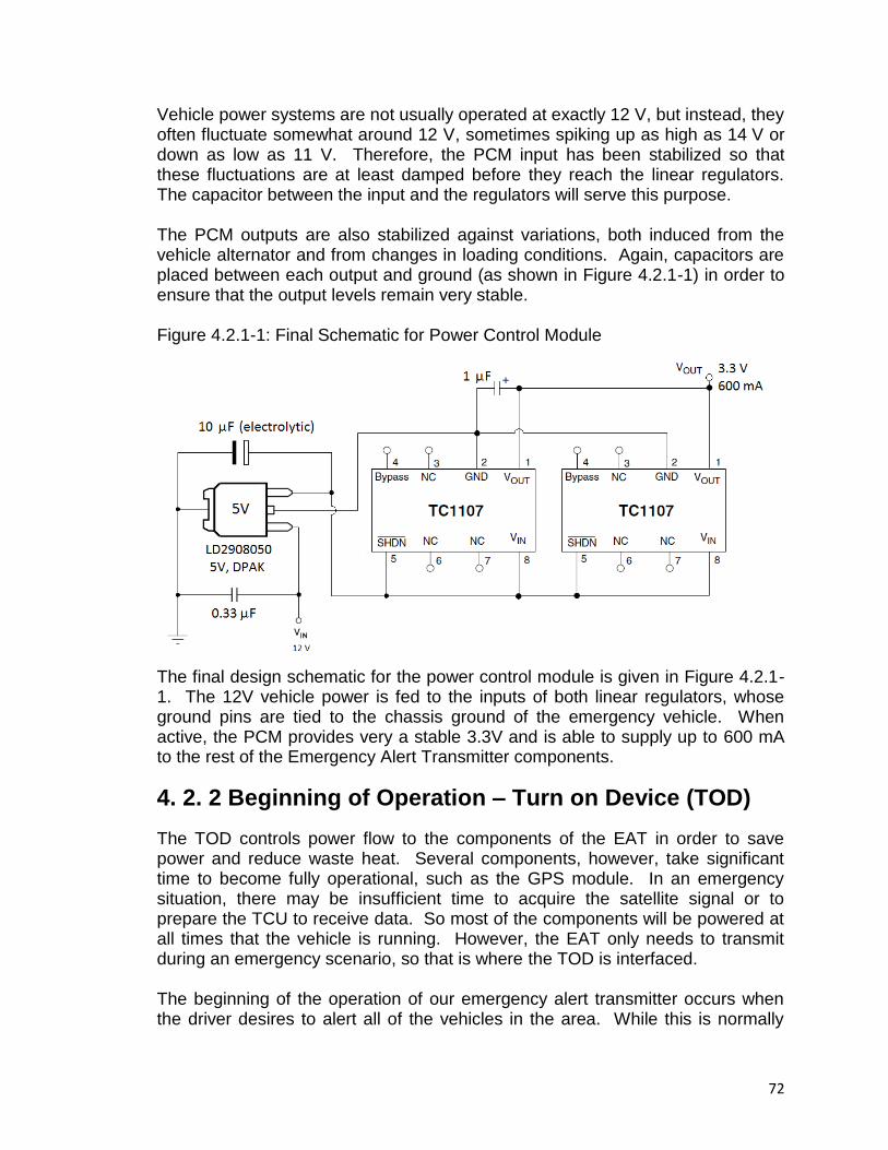
72
Vehicle power systems are not usually operated at exactly 12 V, but instead, they often fluctuate somewhat around 12 V, sometimes spiking up as high as 14 V or down as low as 11 V. Therefore, the PCM input has been stabilized so that these fluctuations are at least damped before they reach the linear regulators. The capacitor between the input and the regulators will serve this purpose. The PCM outputs are also stabilized against variations, both induced from the vehicle alternator and from changes in loading conditions. Again, capacitors are placed between each output and ground (as shown in Figure 4.2.1-1) in order to ensure that the output levels remain very stable. Figure 4.2.1-1: Final Schematic for Power Control Module
The final design schematic for the power control module is given in Figure 4.2.1-1. The 12V vehicle power is fed to the inputs of both linear regulators, whose ground pins are tied to the chassis ground of the emergency vehicle. When active, the PCM provides very a stable 3.3V and is able to supply up to 600 mA to the rest of the Emergency Alert Transmitter components.
4. 2. 2 Beginning of Operation – Turn on Device (TOD)
The TOD controls power flow to the components of the EAT in order to save power and reduce waste heat. Several components, however, take significant time to become fully operational, such as the GPS module. In an emergency situation, there may be insufficient time to acquire the satellite signal or to prepare the TCU to receive data. So most of the components will be powered at all times that the vehicle is running. However, the EAT only needs to transmit during an emergency scenario, so that is where the TOD is interfaced. The beginning of the operation of our emergency alert transmitter occurs when the driver desires to alert all of the vehicles in the area. While this is normally

73
done with lights and sirens, most emergency vehicles also have the ability to operate the lights and sirens independently. It only makes sense to add another switch in the same location that would trigger the emergency alert transmitter in a typical switch box. Once this switch is flipped, the connection between the PCM and the ETD will be enabled, which will then turn on the transmitter. Therefore the turn on device is nothing more than a simple switch which would be installed standard in any emergency vehicle and would simply have to connect the transmitter module to the battery in order to begin transmitting the signal and alerting drivers or the approaching vehicle. The TOD block diagram is shown below in Figure 4.2.2-2. Figure 4.2.2-2: TOD Block Diagram
4. 2. 3 Design of Transmitter Control Unit
Once the transmitter control unit receives the signal informing it to begin transmitting the alert signal, it immediately collects the data from the compass and the GPS sensor and concatenates this information into a single bit stream which is then given to the emergency transmission device for the necessary modulation and transmission of the signal. This involves three interfaces that are integrated into our design: the interface between the transmitter control unit and the compass, the interface with the GPS sensor, and the interface between the transmitter control unit and the transmission antenna.
4. 2. 3. 1 Interfacing the Compass to the Transmitter Control Unit
As explained in the research portion of this documentation, a dsPIC30f4013 was chosen for use as the transmitter control unit. With 40 input and output pins available, the dsPIC30f4013 will have more than enough inputs to interface with all of the necessary components. In order to interface with the HMC6352 compass with the PIC processor, the input voltages and currents must be

74
compared from the data sheets in order to avoid burning out any of our parts. This is also important so that we have an idea of the necessary layout for the printed circuit board and the requirements necessary in the connections, such as pull-up resistors and so on. Upon looking at the data sheet from the HMC6352 compass, the HMC6352 transmits 3.3 volts through an I2C line to the PIC processor which is plenty high enough for the PIC processor to read on the input ports. In order to connect the output line of the HMC6352 compass to the inputs of the dsPIC30f4013, it is also necessary to check the data sheet for the PIC processor in order to observe the maximum and minimum voltage and current ratings for the inputs. The data sheet for the PIC processor shows that the input voltage cannot exceed 5 V. This value is essentially more important to the project than checking the HMC6352 output because it would be more detrimental for the PIC processor to suffer damage because it is more central as well as more expensive. Therefore before any prototype is to be built and any power connected, it is essential to test the individual parts before connecting them to ensure that they observe the behavioral statistics presented in the data sheets. It is also important to consider the need for a pull-up or pull-down resistor to control the value on the line connecting the output of the HMC6352 compass to the PIC processor. Since each output of the Hall Effect compass is an open collector NPN transistor, the output will have two settings: high and low. Since the emitter is grounded, when the logic level is set to low this means that the current (called the sink current) is able to flow through the transistor to the grounded emitter pin, setting a logical value of 0. When the transistor is closed, corresponding to the high level output, the logical value is interpreted to be a 1. This normally requires a pull-up resistor between the supply voltage, Vcc, and the output line so that a set logical high value is maintained. To create the proper voltage that is required for the input of the PIC processor resistors will be connected to accomplish the voltage. To get the proper value for the resistors that are needed one of the most fundamental equations in Electrical Engineering will be used:
V = I * R or R = V / I
The interface protocol that communicates between the compass and the PIC processor uses the I2C protocol. This means that the PIC processor will send commands to the compass and then the compass will send the information that the PIC processor asked for back to the processor. The data rate between the two devices is the standard 100 kbps rate for the I2C protocol. The format of the data bytes are case sensitive ASCII characters. In order to write data to the HMC6352 the slave address is 42(hex) and to command a read operation the value of 43(hex) will be sent over the I2C line. All bus transaction will begin with the master (dsPIC30f4013) device issuing the start sequence followed by the slave (HMC6352) address byte. All the bus transactions will be terminated with
75
the master issuing a stop sequence, the ASCII character “S”. Figure 4.2.3.1-1 shows the interface commands and responses for the HMC6352. Figure 4.2.3.1-1: Interface Commands and Responses
Command byte ASCII
Argument 1
byte
Argument 1
byte
Response 1 byte
Response 1 byte
Description
w (77) EEPROM address
Data N/A N/A Write to EEPROM
r (72) EEPROM address
N/A Data N/A Read from EEPROM
G (47) RAM
address Data N/A N/A Write to RAM Register
g (67) RAM
address N/A Data N/A Read from RAM Register
S (53) N/A N/A N/A N/A Enter Sleep Mode (Sleep)
W (57) N/A N/A N/A N/A Exit Sleep Mode (Wakeup)
O (4F) N/A N/A N/A N/A Update Bridge Offsets (S/R
Now)
C (43) N/A N/A N/A N/A Enter User Calibration Mode
E (45) N/A N/A N/A N/A Exit User Calibration Mode
L (4C) N/A N/A N/A N/A Save Op Mode to EEPROM
A (41) N/A N/A MLB Data LSB Data
Get Data. Compensate and
Calculate New Heading
The HMC6352 contains non-volatile memory capability in the form of EEPROM that stores key operational parameters and setting for the electronic compassing. Figure 4.2.3.1-2 shows the EEPROM locations that the user can read from or write to. Figure 4.2.3.1-2: HMC6352 EEPROM locations
EE Address (hex) Byte Description Factory Default 00 I2C Slave Address 42(hex) 01 Magnetometer X Offset MSB factory test value 02 Magnetometer X Offset LSB factory test value 03 Magnetometer Y Offset MSB factory test value 04 Magnetometer Y Offset LSB factory test value 05 Time Delay (0 – 255 ms) 01(hex)
06 Number of Summed measurements(1-16) 04(hex)
07 Software Version Number >01(hex)
08 Operation Mode Byte 50(hex)
The HMC6352 has three different modes of operation plus the ability to enter/exit the non-operational sleep mode. The sleep mode will put the internal microprocessor into clock shutdown to save power. Since our project is being powered by the vehicle and not batteries and the fact that the compass should always be outputting data while the vehicle is running, the sleep mode will not be used in our application of the compass in our project. The three modes of operation are Standby Mode, Query Mode, and Continues Mode. There is not

76
much difference between the three different modes of operation. When the HMC6352 is put into Continues Mode it continuously output the compass heading without the need the write the command to the compass to get the compass heading. In Query Mode the HMC6352 waits to receive the command to get the compass heading “A” and then continuously sends the compass heading as if it was then in Continues Mode. In Standby Mode, the mode that we are going to use, the HMC6352 waits to receive the command to get the compass heading and then sends the data. It will then what until another receive data command is sent to get another compass heading. This way we will only get the compass headings when we want them.
4. 2. 3. 2 Interfacing the GPS with the Transmitter Control Unit
Another element of the design was the interface of the transmitter control unit to the GPS sensor. Once again it was necessary to check the connection parameters so that neither unit is burned out or damaged because of too much voltage or current. The PIC input characteristics have already been cited as having maximum input voltage of 5 V (only 3.3 V with our design working at 3.3 V), with pull-up resistors that were configured within the PIC. The data sheet for the Global Sat Technology Corporation EM 408 cited that the UART serial lines operated at the TTL standard level, with output line voltages of 0~2.85 V, perfectly within our range. Figure 4.2.3.2-2 shows the completed design application schematic we used as determined with assistance from the data sheet. This output diagram served as the basis for the designed interface between the GPS receiver and the transmitter control unit. The GPS module, the Global Sat Technology Corporation EM 408, that was used in our implemented design of this project was almost a plug in and go device. Only a few external components were needed along with the GPS module. These components were simple pull-up resistors and were used to insure that the GPS module operates at its optimal performance level and the output can be clearly read. To show how the resistors were connected to the GPS module a wiring description is given. Figure 4.2.3.2-1 shows the wiring description for the Global Sat Technology Corporation EM 408.

77
Figure 4.2.3.2-1: EM 408 Pin Descriptions
Pin # Name Description
1 Enable/Disable Connected to Vcc to turn on (leave low to disable)
2 Gnd Grounded to common ground for PIC and GPS
3 Rx Main receive channel for receiving software commands to the engine board from user. Since not in use, this pin must be kept high for operation.
4 Tx This is the main transmit for outputting navigation and measurement data to user‟s software.
5 Vcc Connected to 3.3V DC power supply
From the table above in can be seen that wires 1 (the grey wire) and 5 were connected to the 3.3V line from the PCM in the application of this GPS module in this project. Wire 2 was connected to ground from the PCM and was common between the compass, PIC, and GPS unit. Wire 3 was stated from the data sheet as being tied to high, but during the testing conducted on the parts, the Rx line showed no difference in the operation of the device when not tied to power. Therefore, our design left the wire as an open contact and operation was not inhibited. Since this project does not need to send the GPS module any information, this was an easy task and since it did not inhibit the operation it was not considered a necessary design element. Pin number 4 is the most important line in our design as it sends the information from the unit. The final wire, the fifth wire, was the power supply line that came from the power control module and supplied power the GPS module. This line turned the GPS module on when the vehicle turned on. Pin number 1 is the power ON / OFF control line. This line is able to put the GPS module into a standby mode to conserve power. In standby mode the GPS module has a quicker acquisition rate, the time it takes to fix the GPS module to satellites, than it would from a cold start. Since our design used batteries to simulate the power from the vehicle, there was no need to conserve power in a standby mode. The GPS module was designed to be in the on mode of
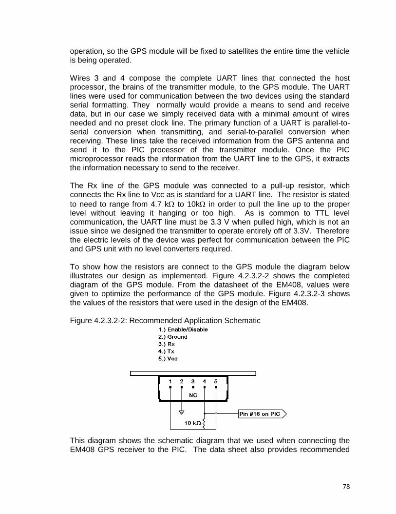
78
operation, so the GPS module will be fixed to satellites the entire time the vehicle is being operated. Wires 3 and 4 compose the complete UART lines that connected the host processor, the brains of the transmitter module, to the GPS module. The UART lines were used for communication between the two devices using the standard serial formatting. They normally would provide a means to send and receive data, but in our case we simply received data with a minimal amount of wires needed and no preset clock line. The primary function of a UART is parallel-to-serial conversion when transmitting, and serial-to-parallel conversion when receiving. These lines take the received information from the GPS antenna and send it to the PIC processor of the transmitter module. Once the PIC microprocessor reads the information from the UART line to the GPS, it extracts the information necessary to send to the receiver. The Rx line of the GPS module was connected to a pull-up resistor, which connects the Rx line to Vcc as is standard for a UART line. The resistor is stated
to need to range from 4.7 k to 10k in order to pull the line up to the proper level without leaving it hanging or too high. As is common to TTL level communication, the UART line must be 3.3 V when pulled high, which is not an issue since we designed the transmitter to operate entirely off of 3.3V. Therefore the electric levels of the device was perfect for communication between the PIC and GPS unit with no level converters required. To show how the resistors are connect to the GPS module the diagram below illustrates our design as implemented. Figure 4.2.3.2-2 shows the completed diagram of the GPS module. From the datasheet of the EM408, values were given to optimize the performance of the GPS module. Figure 4.2.3.2-3 shows the values of the resistors that were used in the design of the EM408. Figure 4.2.3.2-2: Recommended Application Schematic
This diagram shows the schematic diagram that we used when connecting the EM408 GPS receiver to the PIC. The data sheet also provides recommended

79
values to use for the resistors within the circuit; these values are shown in Figure 4.2.3.2-3. Figure 4.2.3.2-3: Recommended Resistor Values
Diagram Part Values Quantity
R1 470 Ohm 1
R2 4.7k~10k Ohm 1
As can be seen in the diagram, the resistor values given by the data sheet were not all included in our design, once again because testing showed that it was not included. The simple connection of the two lines was not enough to establish the UART connection to receive the data as needed. As with any UART connection, several parameters were defined in order for the connection and the data sent along the lines to mean anything. As defined by the UART standards and the data sheet for the GPS unit, a common baud rate must be defined and used by each device so that the sampling rate is correct to obtain the correct number of bits per second. The factory set baud rate from the GPS was given as 4800 bps in the data sheet, a speed that was easily programmed into the PIC. This value was provided in the PIC30F family datasheet tables and was programmed into the baud rate register for the UART connection in the PIC. This software given value established the necessary speed for the asynchronous serial information to be understood. Once the baud rate was set using the MPLAB compiler for the PIC30F4013, it was necessary to understand the NMEA 0183 protocol used by the EM 408 so that the necessary information, such as the latitude and longitude could be extracted from the input and concatenated with the outgoing bit stream that was transmitted. According to the NMEA Reference Manual from SiRF Technology, Inc, the output message format from the GPS module can be selected from among 9 different types of output messages, but came factory programmed to output all 9 in a set pattern. Most of these messages contained numerous words of information that had no correlation to the application of the GPS sensor in the EVADE project, so it was important to properly program the interface with EM 408 so that as little excess information as possible was received. Based on these qualifications, the message format selected for the EVADE project needed to be the GLL or geographic position latitude and longitude message format or the GGA format. It is important to note the message utilizes ASCII code for each letter and symbol, so each individual letter of the code is sent individually along the UART connection since a standard pack size is 8 bits and each ASCII letter is 8 bits long, but must first be converted to a decimal value before being used. The GLL message format is shown in Figure 4.2.3.2-4 along with a table showing the breakdown of the message formatting.

80
Figure 4.2.3.2-4: GLL Message Breakdown
GLL Message Formatting:
Example: $GPGLL,ddmm.mmmm,X,dddmm.mmmm,Y,hhmmss.sss,A,*41,<CR><LF>
Name Section from Example Description
Message ID $GPGLL Standard GLL protocol heading
Latitude ddmm.mmmm Latitude Coordinates
N/S Indicator X N=North, S=South
Longitude dddmm.mmmm Longitude Coordinates
E/W Indicator Y E=East, W=West
UTC Time hhmmss.sss Coordinated Universal Time
Status A A=data valid, V=data not valid
Checksum *41 Error checking count
<CR><LF> <CR><LF> End of message termination
Based on the example and format described in Figure 4.2.3.2-4, this message format contains all of the positional information needed for the EVADE project plus a few additional elements that are useful for checking the validity of the information, but were not used in the project. This message format was compared to the GGA NMEA message format, which is shown in Figure 4.2.3.2-5. This message contained more information than would be needed as well; however, it was one of the standard output messages from the factory programming.
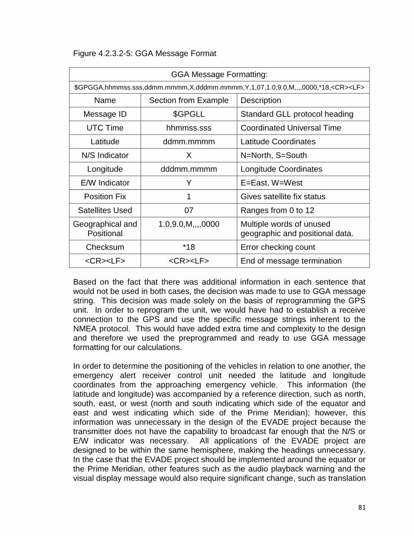
81
Figure 4.2.3.2-5: GGA Message Format
GGA Message Formatting:
$GPGGA,hhmmss.sss,ddmm.mmmm,X,dddmm.mmmm,Y,1,07,1.0,9.0,M,,,,0000,*18,<CR><LF>
Name Section from Example Description
Message ID $GPGLL Standard GLL protocol heading
UTC Time hhmmss.sss Coordinated Universal Time
Latitude ddmm.mmmm Latitude Coordinates
N/S Indicator X N=North, S=South
Longitude dddmm.mmmm Longitude Coordinates
E/W Indicator Y E=East, W=West
Position Fix 1 Gives satellite fix status
Satellites Used 07 Ranges from 0 to 12
Geographical and Positional
1.0,9.0,M,,,,0000 Multiple words of unused geographic and positional data.
Checksum *18 Error checking count
<CR><LF> <CR><LF> End of message termination
Based on the fact that there was additional information in each sentence that would not be used in both cases, the decision was made to use to GGA message string. This decision was made solely on the basis of reprogramming the GPS unit. In order to reprogram the unit, we would have had to establish a receive connection to the GPS and use the specific message strings inherent to the NMEA protocol. This would have added extra time and complexity to the design and therefore we used the preprogrammed and ready to use GGA message formatting for our calculations. In order to determine the positioning of the vehicles in relation to one another, the emergency alert receiver control unit needed the latitude and longitude coordinates from the approaching emergency vehicle. This information (the latitude and longitude) was accompanied by a reference direction, such as north, south, east, or west (north and south indicating which side of the equator and east and west indicating which side of the Prime Meridian); however, this information was unnecessary in the design of the EVADE project because the transmitter does not have the capability to broadcast far enough that the N/S or E/W indicator was necessary. All applications of the EVADE project are designed to be within the same hemisphere, making the headings unnecessary. In the case that the EVADE project should be implemented around the equator or the Prime Meridian, other features such as the audio playback warning and the visual display message would also require significant change, such as translation

82
into a different language. Since the primary designed application was for the North American countries, these considerations are more than sufficient for expansion of the scope of the project and not for our prototype development. In order to ensure that the code ran as quickly as possible, the GPS information was collected in large chunks, much larger than was necessary to capture solely the GGA sentence. Instead, the PIC would store all of the values into an array at once in order to avoid UART receive buffer overflow and then close the UART in order to analyze the data and search for the $GPGGA that indicates the correct sentence. Once this sentence was located, the PIC stored the values of the latitude and longitude within the array and used these locations to output the data in the transmitted string.
4. 2. 3. 3 Completing the Signal to be Transmitted
Once the necessary information had been collected from the compass and the GPS unit, almost all of the information to be transmitted is available. The final two bits of information about the emergency vehicle needed in order for the receiver to function fully are the bits that contain the information about the type of vehicle approaching. Figure 4.2.3.3-1 shows the table of emergency vehicle types and the corresponding two bit code that was assigned for transmission. Figure 4.2.3.3-1: Table of Emergency Vehicle Codes
Emergency Vehicle Type ASCII Value
Police P
Fire F
Ambulance A
Other E
Based on what vehicle type the EVADE transmitter was programmed to be used in, the appropriate two bit code would be hard coded into the dsPIC30F4013 when it is initially programmed. Since this two bit code is not changeable without reprogramming the PIC, the vehicle type that the EVADE module would be installed in must be known ahead of time. This is essential because the receiver must know what type of vehicle is approaching so that the correct audible and visual message could be used to alert the driver. While this hard coded method has the drawback of requiring the vehicle type to be specified at the time of programming, it is only necessary in the transmitter. The receiver has the ability to play back any message for any emergency vehicle type and since the receiver the unit that would be mass produced to be put into every manufactured vehicle, it was essential that the receiver be universally interchangeable. While this hard coded method did affect the vehicle type that the driver receives warning about, it could be switched to a different type of vehicle and still warn the driver of an

83
approaching emergency vehicle, just without specifying the correct vehicle type. This feature was enabled, but not programmed into the prototype in order to demonstrate the functionality of a general unit and not a specified unit. With the powerful ability of the MPLAB and C30 Compiler software that comes with the PIC30F4013, the hard coding of the vehicle type was extremely easy to implement as a simple declaration of a constant character. The most complicated aspect of creating the signal was concatenating the different parts into one continuous bit stream that was easy for the emergency alert receiver to correctly interpret and use. In order to do this, the bits were concatenated in a pre-specified format so that each section of the bit stream had an anticipated range of values. In order to implement this design in the PIC, it was decided that the easiest method was to save the different parts into a preset memory location in the on-chip memory. Using multiple character arrays pre-declared in the main function, several memory locations were allocated so that the bits of information for our signal was saved in the order specified in Figure 4.2.3.3-2. This implementation strategy was easiest because the output bit stream to the transmitter only required the PIC to start at a preset memory word and output each successive word in the array until the end point for the signal is reached, at which point the PIC resets itself to the initial preset memory word for the beginning of the transmission signal process and after a short delay it would repeat the process of reading the signal from memory. Figure 4.2.3.3-2: Signal Stored in Memory
Signal Code Vehicle Type Compass Latitude Longitude
Once the words of data are stored in the proper memory location in the order specified in Figure 4.2.3.3-2, it was extremely easy to program the PIC to output this data as a continuous bit stream by setting the output of the UART pin going to the transmitter antenna to simply output each successive word as it was shifted into the transmit buffer. This was further simplified by the fact that the PIC is accompanied by the MPLAB tool and a five word deep FIFO UART Tx output buffer, which automatically transmits each word with selectable formatting according to the programming of the UART registers. Once the transmit buffer was set up and the word shifted in from memory was completed, the signal was automatically output at 4800 bps to the transmitter and is ready for modulation and transmission to the emergency alert receiver.
4. 2. 4 Design of Modulator and Transmitter Antenna
In the design of the transmitter that is going to be used in this project, the Linx TXM-433-LR, the Linx Company offers a design section in the datasheet that is going to be used to calculate all the values of the external components. In order
5 Bytes 1 Byte 2 Bytes 8 Bytes 9 Bytes
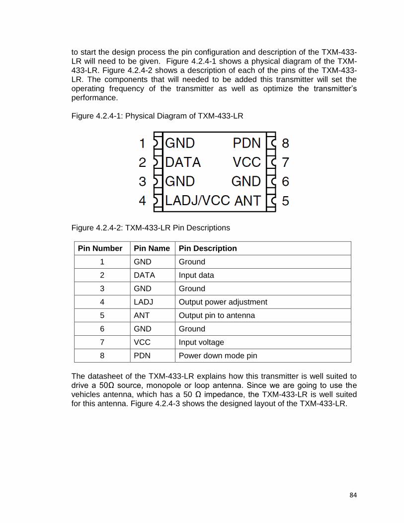
84
to start the design process the pin configuration and description of the TXM-433-LR will need to be given. Figure 4.2.4-1 shows a physical diagram of the TXM-433-LR. Figure 4.2.4-2 shows a description of each of the pins of the TXM-433-LR. The components that will needed to be added this transmitter will set the operating frequency of the transmitter as well as optimize the transmitter‟s performance. Figure 4.2.4-1: Physical Diagram of TXM-433-LR
Figure 4.2.4-2: TXM-433-LR Pin Descriptions
Pin Number Pin Name Pin Description
1 GND Ground
2 DATA Input data
3 GND Ground
4 LADJ Output power adjustment
5 ANT Output pin to antenna
6 GND Ground
7 VCC Input voltage
8 PDN Power down mode pin
The datasheet of the TXM-433-LR explains how this transmitter is well suited to drive a 50Ω source, monopole or loop antenna. Since we are going to use the vehicles antenna, which has a 50 Ω impedance, the TXM-433-LR is well suited for this antenna. Figure 4.2.4-3 shows the designed layout of the TXM-433-LR.
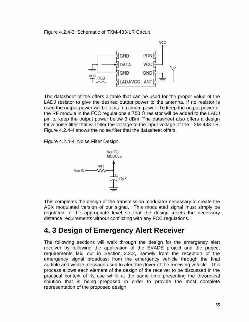
85
Figure 4.2.4-3: Schematic of TXM-433-LR Circuit
The datasheet of the offers a table that can be used for the proper value of the LADJ resistor to give the desired output power to the antenna. If no resistor is used the output power will be at its maximum power. To keep the output power of the RF module in the FCC regulations a 750 Ω resistor will be added to the LADJ pin to keep the output power below 3 dBm. The datasheet also offers a design for a noise filter that will filter the voltage to the input voltage of the TXM-433-LR. Figure 4.2.4-4 shows the noise filter that the datasheet offers. Figure 4.2.4-4: Noise Filter Design
This completes the design of the transmission modulator necessary to create the ASK modulated version of our signal. This modulated signal must simply be regulated to the appropriate level so that the design meets the necessary distance requirements without conflicting with any FCC regulations.
4. 3 Design of Emergency Alert Receiver
The following sections will walk through the design for the emergency alert receiver by following the application of the EVADE project and the project requirements laid out in Section 2.2.2, namely from the reception of the emergency signal broadcast from the emergency vehicle through the final audible and visible message used to alert the driver of the receiving vehicle. This process allows each element of the design of the receiver to be discussed in the practical context of its use while at the same time presenting the theoretical solution that is being proposed in order to provide the most complete representation of the proposed design.

86
4. 3. 1 Power Control Module of Receiver
The Power Control Module (PCM) for the Emergency Alert Receiver (EAR) is nearly identical to the PCM for the Emergency Alert Transmitter except for the fact that it also serves as the turn on device (TOD) for the receiver. After research was performed, it become clear that a turn on device module was not necessary as the entire receiver unit needs to be on and activated the entire time the vehicle is on and in operation. Therefore, the PCM also functions as the turn on device because it will turn on the receiver when the vehicle is started. Besides the effective functionality as the turn on device, the other major difference is that instead of one output voltage level, the EAR PCM supplies two levels: 3.3 V and 5 V. The PCM receives power from the automotive electrical system at 12 V and is under the same stabilization constraints as the previously described PCM. The Turn-On Device for the EAR is a bit more complicated than that of the EAT. The decision to apply power to the rest of the circuit will be determined by an analysis of incoming signals. Only when the EAR verifies an incoming signal to be a genuine emergency transmission will power be delivered to the other components. The TOD functions will thus be handled by the Receiver Control Unit and will not interface directly with the PCM. The input to the PCM will therefore always feel the 12 V from the passenger vehicle battery/alternator on its input as seen in Figure 4.3.1-1, as long as the vehicle is running. The rest of the PCM operation is identical to that of its counterpart in the EAT, except as already noted with respect to the output voltages. For a more complete discussion, see the design section on the Emergency Alert Transmitter PCM. Figure 4.3.1-1: Final Design Schematic for Receiver Power Control Module

87
The final design schematic for the power control module is given in Figure 4.3.1-1. The 12 V input is felt at all times as long as the passenger vehicle in which the system is installed is running. This stabilized 12 V is fed to the input of the 5V regulator, which feeds into the input of the 3.3V regulator. Both regulators ground to the chassis of the passenger vehicle. When active, the PCM provides very stable voltages of 3.3 V and 5 V, each supplying 400 mA to the rest of the EAR components.
4. 3. 2 Receiving the Signal – The Reception Antenna
Once the switch has been flipped and the signal is being broadcast from the emergency vehicle, nothing will be accomplished unless the individual emergency alert receivers inside of every car are able to detect the signal and accurately decode the signal in order to properly alert the driver. The job of the reception antenna in the design is to detect and demodulate the incoming signal from the emergency vehicle and relate that signal to the receiver control unit to decipher the signal and properly alert the driver. In the design of the receiver that is going to be used in this project, the Linx RXM-433-LR, the Linx Company offers a design section in the datasheet that is going to be used to calculate all the values of the external components. In order to start the design process a description of the pin layout of the RXM-433-LR will be given. Figure 4.3.2-2 shows a physical diagram of the RXM-433-LR. Figure 4.3.2-3 shows a description of each of the pins of the RXM-433-LR. Figure 4.3.2-2: Diagram of Linx RXM-433-LR

88
Figure 4.3.2-3: Pin Description for Linx RXM-433-LR
Pin # Pin Name Pin Description
1 NC No connection
2 NC No connection
3 NC No connection
4 GND Ground
5 VCC Input Voltage
6 PND Power down mode pin
7 RSSI Received signal strength indicator
8 DATA Digital input data
9 NC No connection
10 NC No connection
11 NC No connection
12 NC No connection
13 NC No connection
14 NC No connection
15 GND Ground
16 RF-IN 50 Ω RF input
The datasheet of the RXM-433-LR explains how this receiver is well suited to work with a 50Ω source, monopole or loop antenna. Since we are going to use the vehicles antenna, which has a 50 Ω impedance, the RXM-433-LR is well suited for this antenna. Figure 4.3.2-3 shows the designed layout of the RXM-433-LR. Figure 4.3.2-3: Schematic of Linx RX-433-LR
An additional design step was strongly recommended by the datasheet, antenna impedance matching. This design step is to match the impedance of the antenna to the impedance of the input of the IC. The impedance of a coaxial car antenna is 50Ω. To match this impedance the datasheet gives a table of inductor values that will match this impedance to the impedance of the input of the IC. The two inductors and their values that will be needed to match the impedance for this antenna are LSHUNT = 15 nH and LSERIES = 72 nH. Figure 4.3.2-4 shows the
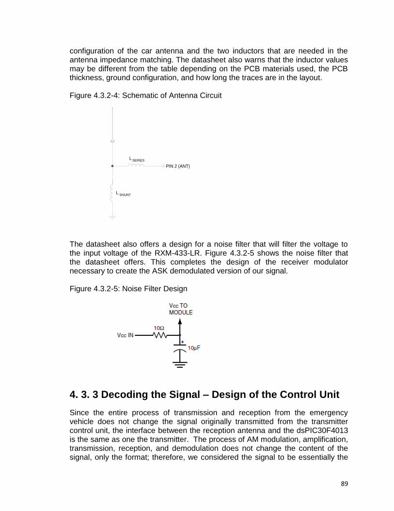
89
configuration of the car antenna and the two inductors that are needed in the antenna impedance matching. The datasheet also warns that the inductor values may be different from the table depending on the PCB materials used, the PCB thickness, ground configuration, and how long the traces are in the layout. Figure 4.3.2-4: Schematic of Antenna Circuit
PIN 2 (ANT)
SHUNTL
L SERIES
The datasheet also offers a design for a noise filter that will filter the voltage to the input voltage of the RXM-433-LR. Figure 4.3.2-5 shows the noise filter that the datasheet offers. This completes the design of the receiver modulator necessary to create the ASK demodulated version of our signal. Figure 4.3.2-5: Noise Filter Design
4. 3. 3 Decoding the Signal – Design of the Control Unit
Since the entire process of transmission and reception from the emergency vehicle does not change the signal originally transmitted from the transmitter control unit, the interface between the reception antenna and the dsPIC30F4013 is the same as one the transmitter. The process of AM modulation, amplification, transmission, reception, and demodulation does not change the content of the signal, only the format; therefore, we considered the signal to be essentially the

90
same when designing the interface to the PIC. The only factor played a role is the introduction of noise or interference during the transmission; however, the amplification of the signal made the signal to noise ratio large enough that the noise did not make the signal unrecognizable after demodulation.
Very similar to how the original signal was read from memory and sent to the transmitter in order to be broadcast, the received signal was interfaced the same way with the receiver control unit. As the information is being collected from the reception antenna, our dsPIC30F4013 in the receiver control unit stored the signal in a pre-specified location in the on-chip memory. As described in Section 4. 2. 3, the necessary steps to correctly save the incoming signal are made very easy by the UART protocols and tools as well as array declarations that accompanied the MPLAB software standard with the dsPIC30F4013.
Once the emergency signal array for receiving the incoming signal has been filled in the proper memory location, the PIC began the most important task of properly using all of the data that was collected. The receiver control unit has the exact same interface with the Hall effect compass and the GPS sensor in the receiving vehicle as has been previously discussed for the transmitter control unit. For more information on the design of these interfaces, see Section 4. 2. 3. 1 and Section 4. 2. 3. 2. This information was used to determine the heading of the vehicle in relation to the emergency vehicle broadcasting the signal; in order for this to be done, the GPS coordinates were also used to determine which vehicle is farther north or west.
GPS measurements were taken with respect to the angle from the equator or the Prime Meridian. The latitude coordinates were given in degrees and minutes measured from the equator, which in the case of this project was the number of degrees above the equator since the designed area for application is in the United States, which is entirely within the northern hemisphere. Therefore the larger the value given for the latitude, the farther north the point; the limiting value for the latitude would be 90 degrees, located at the North Pole. In the same way, longitude is the horizontal measurement of distance from the Prime Meridian, once again measured in degrees and minutes; the design for the EVADE project only considered points in the western hemisphere, which can range up to 180 degrees from the Prime Meridian, where the 180 degree point is the International Date Line. Therefore, when considering the values measured by the GPS for this project, the larger the longitudinal value, the farther west the point is.
Since the latitude and longitude values determined relatively how far west and north the vehicles are located, the difference between the latitude and longitude values determined which vehicle is farther north and farther west. Considering the receiving vehicle to be at the origin of a standard Cartesian coordinate system, we took the difference of coordinates in order to give the location of the emergency vehicle relative to the receiving vehicle in four quadrants. The difference of the receiving vehicle‟s coordinates minus the emergency vehicles coordinates created four possible quadrants as shown in Figure 4.3.3-1. Once the quadrant was determined, the directional headings of both compasses were

91
considered in order to determine if it was appropriate to alert the driver. If the emergency vehicle was northeast of the driver, but was headed farther east so that there should be no intersection of paths, it was not necessary to alert the driver since the driver should not intersect the path of the emergency vehicle.
Figure 4.3.3-1: Condition of Intersection as Calculated from Directional Headings
QUADRANT( + , + )
NNW
W
QUADRANT( - , + )
QUADRANT( + , - )
QUADRANT( - , - )
E
NEN
SSE
E
SWS
W
However, if the emergency vehicle was to perform a U-turn and begin heading back towards the receiving vehicle, the driver was warned since there was now a possible intersection of the two paths. This boiled down the directions indicated by the emergency vehicle‟s compass to only those indicated in Figure 4.3.3-1 since only those directions had a possible intersection with the receiving vehicle‟s path. The table and diagram shown in Figure 4.3.3-1 and Figure 4.3.3-2 made the breakdown of conditions for an alert extremely simple to understand visually and easy to program using a series of if and else if statements.

92
Figure 4.3.3-2: Determined if Statements for Directional Headings
Car Direction Emergency Vehicle Direction If Statement
North If North and Quad (+,-) or Quad (+,+) -> Alert “Rear”
North If South and Quad (-,-) or Quad (-,+) -> Alert “Front”
North If East and Quad (+,-) or Quad (-,-) -> Alert “Left”
North If West and Quad (+,+) or Quad (-,+) -> Alert “Right”
South If North and Quad (+,-) or Quad (+,+) -> Alert “Front”
South If South and Quad (-,-) or Quad (-,+) -> Alert “Rear”
South If East and Quad (+,-) or Quad (-,-) -> Alert “Right”
South If West and Quad (+,+) or Quad (-,+) -> Alert “Left”
East If North and Quad (+,-) or Quad (+,+) -> Alert “Left”
East If South and Quad (-,-) or Quad (-,+) -> Alert “Right”
East If East and Quad (+,-) or Quad (-,-) -> Alert “Rear”
East If West and Quad (+,+) or Quad (-,+) -> Alert “Front”
West If North and Quad (+,-) or Quad (+,+) -> Alert “Right”
West If South and Quad (-,-) or Quad (-,+) -> Alert “Left”
West If East and Quad (+,-) or Quad (-,-) -> Alert “Front”
West If West and Quad (+,+) or Quad (-,+) -> Alert “Rear”
It can be observed from Figure 4.3.3-2 that only four main alert message groups needed to be formed in the memory of the controller; one for the case where the emergency vehicle was approaching from the left, right, front, or rear. One case that was not shown in the table is the situation where the emergency vehicle was approaching from one of the intermediate directions, namely NE, NW, SE, or SW. In this case the logical if statements might not detect any of the correct cases; therefore, when the heading was in one of the intermediate states, the difference in latitude and longitude was compared. Comparing the two differences in latitude and longitude values allowed the control unit to determine if the approaching vehicle was closer from the front/rear or from the left/right. If the vehicle was closer to the left or right of the vehicle, then it was more likely that the two vehicles will meet in a situation where the emergency vehicle would be more easily visible on the vehicle‟s left or right side; therefore that is direction that was related to the driver. This breakdown of cardinal directions and any intermediate cases completed the design of the controller interface with the

93
information from the received signal and the Hall-effect compass and GPS; from this point, the receiver control unit alerted the driver based on the direction already determined.
4. 3. 4 Interface of Audio/Visual Warnings
Once the proper heading has been determined, the next key step is to alert the driver using an audible message played back across the vehicle‟s stereo system as well as a message displayed on a visual display on the dashboard. This final section of the design is fairly simple, yet the entire EVADE project hinges on the proper functionality of these units in order to actually alert the driver and make the project successful. The interfacing of the recorded audible alert system and the visual display system will require a significant amount of memory, practically to the point of maxing out the amount of on-chip memory available on the PICds30. Therefore, the RAA and VDU have been allocated with their own microprocessors to control their input and output and allow them to act as stand-alone units, only requiring input signal from the PIC microcontroller to determine the correct signal to play or display respectively.
4. 3. 4. 1 Interfacing the Recorded Audible Alert
One of the main distractions that inhibits a driver‟s ability to perceive an approaching emergency vehicle is the volume of their stereo system. It was determined in the research section of this document that the EVADE project could help overcome this obstacle by adding an audio bypass that would turn off the stereo and play back a pre-recorded message once the transmitted signal is detected from an approaching emergency vehicle. This message is sent through the stereo lines of the vehicle to the switching bypass unit, which is then required to switch between the driver‟s stereo output and the pre-recorded message when appropriate.
Playing Back the Message Based on the research conducted to investigate the possible implementations of the recorded audible alert, the group chose to use pre-recorded wav files for the alert messages. The messages are stored on the onboard Flash memory of the Nuvoton ISD1760 ChipCorder, which is controlled via SPI interface by an ATmega328 microcontroller. Figure 4.3.4.1-1 shows the RAA schematic, including both chips as well as the SBU. The MIC input was used for programming the ISD1760 on the breadboard. Since the PCB layout included DIP headers, the ISD1760 could be easily removed for reprogramming, and thus the MIC input was omitted from the final PCB design.

94
Figure 4.3.4.1-1: RAA/SBU Schematic
The Nuvoton ChipCorder has ample Flash memory for storing all of the alert messages. Each alert message was recorded into an individual .wav file on a PC, then transferred to the ChipCorder using a custom built cable via the MIC input on pins 10 and 11. The AnaIn (pin 9) was found to provide insufficient amplification upon playback, and was therefore not used. Prior to recording the final alert messages, a global erase function was performed so that no residual test messages remained. On power-up/reset, the ChipCorder initialized its PLAY and REC pointers at the first memory location. Using the custom audio cable, the ChipCorder was interfaced with the PC via the headphone jack. The alert messages were played in Windows Media Player, one by one, as the ChipCorder recorded. In addition to the stand-alone mode used to record on the ChipCorder, the ISD1760 is also capable of operating in SPI mode. An ATmega328 serves as the RAA microcontroller and was programmed on the Arduino Uno development board. The RAA microcontroller interfaces with the ISD1760 via SPI. The microcontroller receives as input a 3-bit binary signal from the RCU on pins 28, 27, and 26 (MSB → LSB) and uses this signal to determine the appropriate emergency alert message to play. Additionally, when a valid alert signal is received from the RCU, the ATmega328 sets its pin 4 high, which ties into the

95
control line of the SBU control relay, causing the SBU to bypass the stereo signal.
Design of Switching Bypass Unit After comparing the possible options for implementing the function of the switching bypass unit as discussed in the research portion of this document (see Section 3. 3. 5), we decided that the best choice was the electromechanical relay, which can be seen in the block diagram in Figure 4.3.4.1-2. The relay is small enough to be mounted onto a printed circuit board, which makes incorporating into our overall design very simple. Also, the relay consumes low power, and has a high switching speed with no noticeable bounce effect. One relay is used for each channel. Figure 4.3.4.1-2 Switching Bypass Unit Design Schematic
The relays chosen for bypassing the car stereo are rated for automobile applications and require at least 4V to trigger. However, the RCU is only able to supply a 3.3V control signal, so an additional relay was added and is labeled

96
CNTRL Relay in Fig.4.3.4.1-2. The steady-state input on the CNTRL relay is tied to ground, while its secondary input is tied to 5V. Under normal operating conditions when no emergency alert message is warranted, the control line on the CNTRL relay will be at ground (logic state “0”), passing the primary signal (also ground) to the bypass relays. This keeps them de-energized, allowing the signals from the stereo lines (if any) to pass to the car‟s installed speakers. When an emergency alert message is generated, the RCU will set the control line to 3.3V (logic state “1”), which passes the secondary input (5V) to the bypass relays, activating them. This allows the signal from the recordable audible alert module to pass to the speakers, bypassing the stereo signal (if present). This setup allows a complete bypass of the speaker lines so that the system functions regardless of whether or not the stereo is in use by the occupant. The signal from the recordable audible alert module splits into 2 individual lines (one for each of the front speakers in the passenger vehicle). Only the front speakers are currently handled in the design. A production model would bypass all of the vehicle‟s speakers.
4. 3. 4. 2 Interface of Visual Display Unit
The visual display unit was designed to alert the driver using both an LED text display as well as several LEDs on the outside edge of the display; these displays will operate in different ways depending on whether the receiver detects an alert condition or if it is in normal operation. When the vehicle is in normal operation and no alert message is detected, the visual display will function as a normal compass for the vehicle, displaying the current directional heading. This is a very simple interface since it only requires the Hall-effect compass of the vehicle to be connected to the eight different display messages located in the memory. Therefore, as the vehicle is moving, the receiver control unit will simply map the Hall-effect output to the correct LED text message sequence in memory. In this operation mode, the LED lights on the outside edge of the display will remain off and only the directional message will be displayed. Once an alert condition is detected, the receiver control unit will change the alert message to relate the correct direction of the approaching emergency vehicle as well as light up the LED on the edge of the display correlating to that direction. Figure 4.3.4.2-1 shows a sample of possible situations that might be encountered for every directional heading and the appropriate message that should be displayed as well as the appropriate edge LED light that should be illuminated. The full table may be found in Appendix A-1.
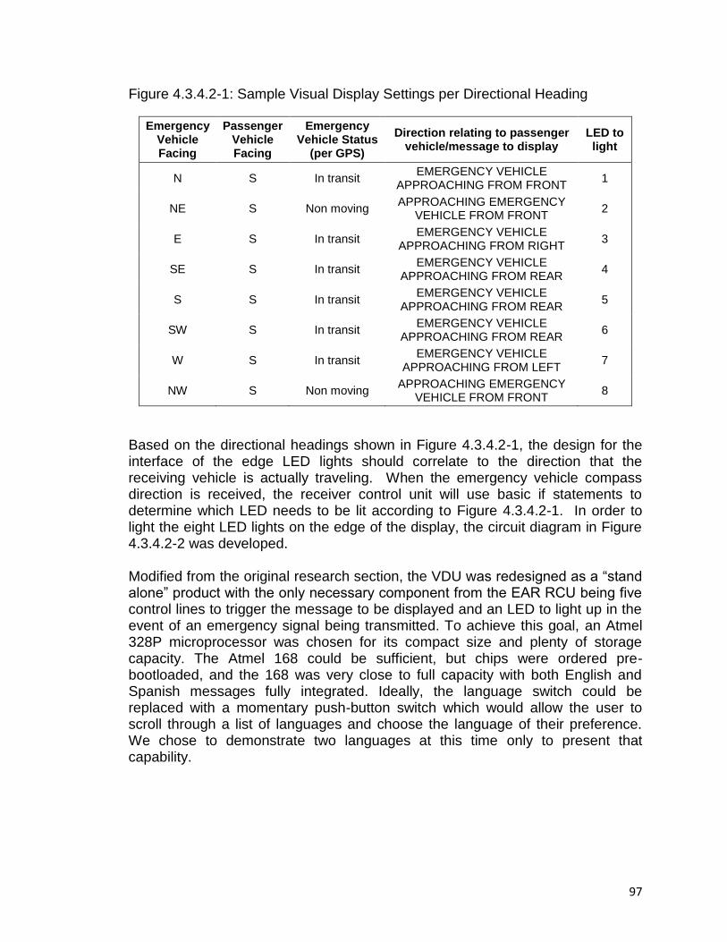
97
Figure 4.3.4.2-1: Sample Visual Display Settings per Directional Heading
Emergency Vehicle Facing
Passenger Vehicle Facing
Emergency Vehicle Status
(per GPS)
Direction relating to passenger vehicle/message to display
LED to light
N S In transit EMERGENCY VEHICLE
APPROACHING FROM FRONT 1
NE S Non moving APPROACHING EMERGENCY
VEHICLE FROM FRONT 2
E S In transit EMERGENCY VEHICLE
APPROACHING FROM RIGHT 3
SE S In transit EMERGENCY VEHICLE
APPROACHING FROM REAR 4
S S In transit EMERGENCY VEHICLE
APPROACHING FROM REAR 5
SW S In transit EMERGENCY VEHICLE
APPROACHING FROM REAR 6
W S In transit EMERGENCY VEHICLE
APPROACHING FROM LEFT 7
NW S Non moving APPROACHING EMERGENCY
VEHICLE FROM FRONT 8
Based on the directional headings shown in Figure 4.3.4.2-1, the design for the interface of the edge LED lights should correlate to the direction that the receiving vehicle is actually traveling. When the emergency vehicle compass direction is received, the receiver control unit will use basic if statements to determine which LED needs to be lit according to Figure 4.3.4.2-1. In order to light the eight LED lights on the edge of the display, the circuit diagram in Figure 4.3.4.2-2 was developed. Modified from the original research section, the VDU was redesigned as a “stand alone” product with the only necessary component from the EAR RCU being five control lines to trigger the message to be displayed and an LED to light up in the event of an emergency signal being transmitted. To achieve this goal, an Atmel 328P microprocessor was chosen for its compact size and plenty of storage capacity. The Atmel 168 could be sufficient, but chips were ordered pre-bootloaded, and the 168 was very close to full capacity with both English and Spanish messages fully integrated. Ideally, the language switch could be replaced with a momentary push-button switch which would allow the user to scroll through a list of languages and choose the language of their preference. We chose to demonstrate two languages at this time only to present that capability.
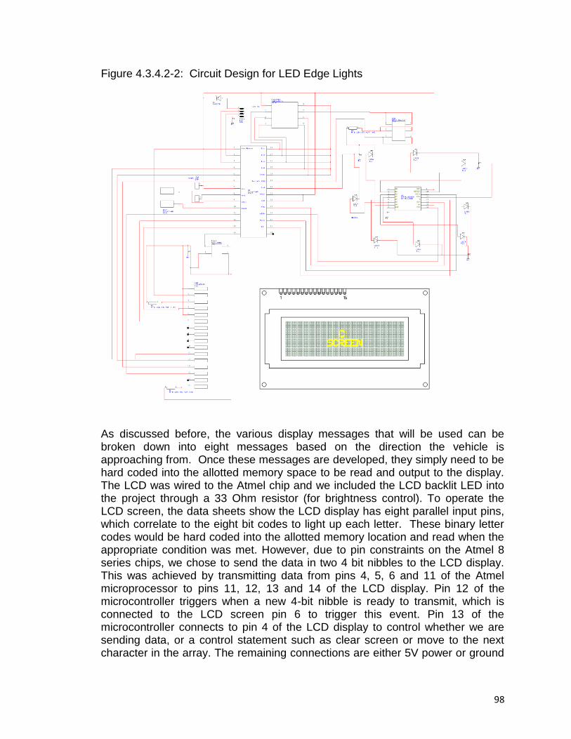
98
Figure 4.3.4.2-2: Circuit Design for LED Edge Lights
As discussed before, the various display messages that will be used can be broken down into eight messages based on the direction the vehicle is approaching from. Once these messages are developed, they simply need to be hard coded into the allotted memory space to be read and output to the display. The LCD was wired to the Atmel chip and we included the LCD backlit LED into the project through a 33 Ohm resistor (for brightness control). To operate the LCD screen, the data sheets show the LCD display has eight parallel input pins, which correlate to the eight bit codes to light up each letter. These binary letter codes would be hard coded into the allotted memory location and read when the appropriate condition was met. However, due to pin constraints on the Atmel 8 series chips, we chose to send the data in two 4 bit nibbles to the LCD display. This was achieved by transmitting data from pins 4, 5, 6 and 11 of the Atmel microprocessor to pins 11, 12, 13 and 14 of the LCD display. Pin 12 of the microcontroller triggers when a new 4-bit nibble is ready to transmit, which is connected to the LCD screen pin 6 to trigger this event. Pin 13 of the microcontroller connects to pin 4 of the LCD display to control whether we are sending data, or a control statement such as clear screen or move to the next character in the array. The remaining connections are either 5V power or ground

99
with the exception of pin 3 of the LCD display runs through a 1000 Ohm resistor to control the contrast. For future development, a variable resistor may be included here and connected to the LCD bezel to allow the user to control the contrast via a knob, or momentary switch that would step through incremental contrast setting controlled by the program. With the incorporation of the integrated HD44780 display driver, the need for programming the individual hexadecimal letter codes directly to the LCD input ports became unnecessary. The Hitachi driver converts the strings sent from the microprocessor into the appropriate 8-bit letter codes and displays them to the screen. The following table is an example of the bit-code and corresponding hexadecimal code that the HD44780 converts each character into prior to sending the final information to the LCD. Figure 4.3.4.2-3: Visual Display Letter Codes
8 Bit and Hexadecimal Letter Codes
0010 0000 = 20 = (space) 0100 1001 = 49 = “I” 0101 0010 = 52 = “R”
0100 0001 = 41 = “A” 0100 1010 = 4A = “J” 0101 0011 = 53 = “S”
0100 0010 = 42 = “B” 0100 1011 = 4B = “K” 0101 0100 = 54 = “T”
0100 0011 = 43 = “C” 0100 1100 = 4C = “L” 0101 0101 = 55 = “U”
0100 0100 = 44 = “D” 0100 1101 = 4D = “M” 0101 0110 = 56 = “V”
0100 0101 = 45 = “E” 0100 1110 = 4E = “N” 0101 0111 = 57 = “W”
0100 0110 = 46 = “F” 0100 1111 = 4F = “O” 0101 1000 = 58 = “X”
0100 0111= 47 = “G” 0101 0000 = 50 = “P” 0101 1001 = 59 = “Y”
0100 1000 = 48 = “H” 0101 0001 = 51 = “Q” 0101 1010 = 5A = “Z”
The messages were programmed as a line-by-line set of code so that each line displayed correctly. Then the group of four lines was grouped as a set, and then the microcontroller was used to choose the set of lines to display. These “sets” were subroutines within the C code programming and when called, transferred variable date for each line to the main program to execute and transmit to the LCD screen. Both messages for English and Spanish have been hard coded onto the chip and ready for display via a SPST (on/off) switch. As mentioned earlier, a momentary switch could replace this switch as a solution to achieve multiple languages. After the correct message is determined by the control lines sent from the RCU to the VDU microcontroller, the microcontroller will display the correct message. The RCU connects to the VDU microcontroller through pins 24 through 28 on the VDU microcontroller. Pin 23 of the microcontroller is connected to the language switch. Another problem arose with using all of the pins mentioned thus far, the eight LED‟s around the bezel of the LCD still needed to be controlled by the VDU

100
microcontroller. Pins on the microcontroller were now at a premium, and there was not eight pins to utilize to control the LED‟s. The solution was to add an 8-bit shift register to the design, and control the shift register through the SPI lines of the microprocessor. This required only three pins of the microprocessor, but could control the eight LED‟s by sending an eight segment bit code to the shift register. Also, this made the coding very apparent as to which LED would be lit during each message sequence. The part chosen to implement this portion of the design phase was the Texas Instruments SN74HC595 Flip-Flop/Latch/Shift register. This part was chosen due to Texas Instruments record of low power consumption, and ease of latching capability. Thus far, the power requirements for the VDU had been steadily climbing with the addition of its own microcontroller and now this additional shift register to deal with. The SN74HC595 proved to be an excellent component and worked flawlessly. Bit code was sent from the VDU microprocessor to the shift register through the SPI interface of the processor and the shift register handled the rest beautifully. There was another dilemma, however, the power requirements of adding a microprocessor, and a shift register, to the current load provided by the PCM for the EAR was inadequate. The VDU had exceeded the 500 mA originally considered. Now, the VDU was pulling between 850 and 900 mA. The solution for this was to give the VDU its own LM7805 5V regulator to allow the VDU to draw the necessary current from the vehicle‟s electrical system. The final VDU PCB design is displayed below. Figure 4.3.4.2-4: VDU PCB design:

101
5. Prototype
The specified design from Section 4 describes the integration of all of the parts and components necessary for the project; this section describes the prototypes that were built in order to test the design and create a final, working prototype. To integrate the parts a list of each of the parts needed to be known. A list was made for the Emergency Alert Transmitter and for the Emergency Alert Receiver. The rest of the components that are not listed in the Emergency Alert Transmitter and the Emergency Alert Receiver are parts that are being used on the vehicle. All the capacitors, resistors, and inductors that were used are not listed because they are extremely low cost and will be bought in bulk.
5. 1 Acquiring Parts: Emergency Alert Transmitter
The components necessary for implementing the Emergency Alert Transmitter are shown in Figure 5.1-1. Parts were ordered by the group member primarily responsible for that functional block. Part cost does not include shipping charges.
Figure 5.1-1: Emergency Alert Transmitter Component Costs
Part Manufacturer Part Number Cost Purchase
Site
Linear Voltage
Regulator
ST
Microelectronics LD2908050 $1.56 Digi-Key
Linear Voltage
Regulator Microchip TC1107 $0.92 Digi-Key
Microcontroller Microchip dsPIC30F4013 Free Microchip
Hall-Effect
Compass Honeywell HMC6352 $34.95 SparkFun
GPS Antenna
Module USGlobalSat EM - 408 $47.99 USGlobalSat
Transmitter Linx RXM-433-LR $28.95 Reynolds Electronics
Antenna Linx RA-ANT $3.40 Reynolds Electronics
5. 2 Acquiring Parts Emergency Alert Receiver
The components necessary for implementing the Emergency Alert Receiver are shown in Figure 5.2-1. Parts were ordered by the group member primarily
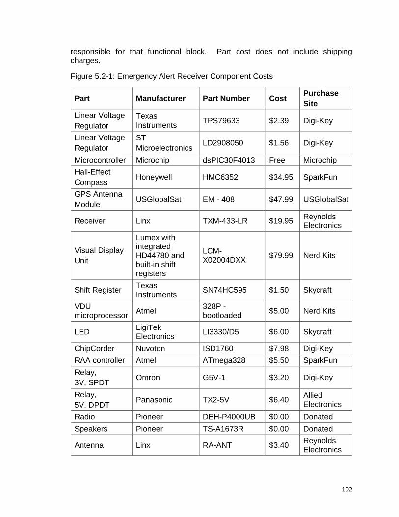
102
responsible for that functional block. Part cost does not include shipping charges.
Figure 5.2-1: Emergency Alert Receiver Component Costs
Part Manufacturer Part Number Cost Purchase
Site
Linear Voltage
Regulator
Texas Instruments
TPS79633 $2.39 Digi-Key
Linear Voltage
Regulator
ST
Microelectronics LD2908050 $1.56 Digi-Key
Microcontroller Microchip dsPIC30F4013 Free Microchip
Hall-Effect
Compass Honeywell HMC6352 $34.95 SparkFun
GPS Antenna
Module USGlobalSat EM - 408 $47.99 USGlobalSat
Receiver Linx TXM-433-LR $19.95 Reynolds Electronics
Visual Display
Unit
Lumex with integrated HD44780 and built-in shift registers
LCM-X02004DXX
$79.99 Nerd Kits
Shift Register Texas Instruments
SN74HC595 $1.50 Skycraft
VDU microprocessor
Atmel 328P - bootloaded
$5.00 Nerd Kits
LED LigiTek Electronics
LI3330/D5 $6.00 Skycraft
ChipCorder Nuvoton ISD1760 $7.98 Digi-Key
RAA controller Atmel ATmega328 $5.50 SparkFun
Relay,
3V, SPDT Omron G5V-1 $3.20 Digi-Key
Relay,
5V, DPDT Panasonic TX2-5V $6.40
Allied Electronics
Radio Pioneer DEH-P4000UB $0.00 Donated
Speakers Pioneer TS-A1673R $0.00 Donated
Antenna Linx RA-ANT $3.40 Reynolds Electronics

103
5. 3 Assembly
In order to assemble the individual components and create the initial circuits, several solderless breadboards were used. Once these breadboards were assembled, testing was conducted to verify that the components worked together, and that the completed circuit performed as expected. Additionally, the type of connectors for the antenna and speakers were determined during this stage to allow connection to any vehicle after production of the printed circuit board. After the parts were assembled on the breadboards, and all circuits were connected and tested, the layout for the printed circuit board (PCB) was created. The PCB diagrams are also known as Gerber files. The name Gerber file is used because the Gerber Systems Corporation published a reference manual titled “GERBER FORMAT, Plot Data Format Reference Book”. In the early 80‟s, the Gerber Systems Corporation had a photoplotter machine which was used in PCB manufacturing. Later, the term Gerber files was adopted by other manufacturers and became the industry standard.
5. 4 Printed Circuit Board Design
To design a PCB, many drawings, or layers, are created to model the design of the final product. Many manufacturers today refer to the Gerber layering standard, and insist the filename extensions match this standard when ordering a PCB to be created. The standard filename extensions are as follows:
.GBL - Gerber Bottom Layer .GTL - Gerber Top Layer .GBS - Gerber Bottom Solder Resist .GTS - Gerber Top Solder Resist .GBO - Gerber Bottom Overlay .GTO - Gerber Top Overlay .GBP - Gerber Bottom Paste .GTP - Gerber Top Paste .GKO - Gerber Keep-Out Layer .GM1 - Gerber Mechanical 1 .GM2 - Gerber Mechanical 2 .GPT - Gerber Top Pad Master .GPB - Gerber Bottom Pad Master
The reason for the individual filenames is to standardize the Computer Numerically Controlled (CNC) machines that will produce the PCB‟s. The GBL layer is used on a two sided PCB as the bottom trace layer for connecting the components. The GBT layer is used for the trace layer on top of the PCB. The next two layers, the GBS and GTS layers are the bottom and top solder resist layers, which helps to keep the solder from connecting two or more

104
traces inadvertently during assembly. The next two layers, the GBO and GTO are the bottom and top silkscreen layers that identify parts, pin numbers, PCB name, and any other important markings that enable the manufacturer to identify the parts and external connections after the PCB has been created. The next two layers, the GBP and GTP are the paste layers to surface mount the individual components to the PCB. The GKO layer is used to mask out certain portions of the PCB. This layer is seldom required for most applications. The GM1 and GM2 layers are the mechanical layers which tell the CNC machine where to drill holes for the pinouts of the components as well as holes for the vias. The vias are holes with metal inserts that connect the top layer to the bottom layer to allow the traces to stop at one point on one side of the board, and continue from that point on the other side of the board. This is helpful when routing becomes difficult due to overcrowding of components on one side of the board, or when components are mounted on opposite sides of the PCB. The final two layers, the GPT and GPB, are used to create the solder pads necessary to connect external components and wires to the PCB. The plans for the PCB will be drawn up on AutoCAD software, and then transferred to PCB Artist software to test the continuity of the traces, and determine any interference problems found with the diagrams and layers. Once these diagrams have been designed, the components, connectors, and diagrams will be delivered to the PCB manufacturer to create the PCB. Once the PCB manufacturer has completed the PCB, the part returned will be ready for the components to be mounted to the board. Once mounted, the boards may be tested, then fitted into the housing that will go into the vehicles.
5. 5 Housing Design
The design of the housing for the EAT module, the EAR module, and the VDU were designed to allow the PCB‟s of each module to be mounted into the receiving vehicles. The design of the housing for the EAT and EAR portions of the project were designed to allow the components, specifically the Hall-effect compass and the GPS module, to be mounted in the vehicle as to not exceed the twelve degrees of tilt. Essentially, mounting within the vehicles should ideally be horizontal with zero degrees of tilt. The housing for the VDU was designed to be somewhat aesthetically pleasing so as to not interfere with the overall design of the car dashboard, yet still be functional.

105
6. Testing
Testing was conducted in three primary phases. Within each phase, tests were designed to isolate the smallest number of functional blocks possible so if an error occurred, it would be easier to trace the fault and fix the problem. Testing methods varied somewhat from one module to the next as the situation dictated. But in general, tests included voltage and current measurements, temperature measurements, and signal analysis. The required test equipment and the purpose of each is summarized in Figure 6.1-1. Additional equipment may be added as the need arises. Figure 6.1-1: Necessary Testing Equipment List
Equipment Manufacturer Purpose
Oscilloscope Tektronix Voltage and current measurements, variations
Digital Multimeter Fluke Point voltage and current measurements, dc
Power Supply Stable power, for testing
Hand Compass Silva Starter 123 Verifying HEC
6. 1 Component Testing
Testing Phase I consisted of testing individual components and modules as they were mounted on breadboards. Proper functioning of the individual modules was ascertained with the highest level of isolation before integrating larger blocks together. This greatly simplified troubleshooting as faults were detected. As modules were integrated, proper communication between components become the primary focus. Problems at this stage can be rectified, and design changes, if needed, can be easily implemented. Phase I testing will be conducted in a lab setting where outside interference can be kept to a minimum.
6. 1. 1 Power Control Module
The power control modules must supply the correct power profile within fairly strict tolerances in order for the system as a whole to function properly. If the power is not properly conditioned, not only may various devices not work, but damage may be caused to some of the more sensitive parts. As such it was imperative to thoroughly test the PCM before committing it to a printed circuit board. The design specifications for the PCMs, as listed in sections 2.1.1.1 and 2.1.2.1, are repeated below.
Operate on 12V Tolerate voltage spikes or drops from the vehicle alternator Deliver 5V and 3.3V outputs Not introduce radio frequency interference (RFI) to the transmitter

106
Since the voltage regulators ordered were surface-mount parts, they could not be assembled and tested on breadboards. Instead, perforated boards were used to solder the regulators and capacitors together. The regulators were tested individually with simulated loads, then put together as complete modules and tested again. The input voltage was varied over the range expected from a car battery/alternator setup to ensure a steady output was maintained. Then the voltage was quickly driven up to the maximum expected voltage in order to simulate a voltage spike in the system, as can easily occur in a real vehicle. Then the voltage was quickly reduced to the minimum range to simulate a change in loading conditions. During each of these tests, each output line was monitored using an oscilloscope to measure the RMS voltage output as well as the ripple voltage. All of the voltage regulators maintained steady output voltages (5V and 3.3V) within the tolerances of the components that would be drawing power from the PCM. These voltages were maintained during the steady operation (12V), the spike up, and the spike down tests. Output current on each line was also monitored to ensure compliance with the data sheets. Under all test conditions, the regulators performed as expected.
6. 1. 2 Hall-effect Compass
The documentation for the Dinsmore Hall-effect compass (Sensor No. 1490) was not as clearly written as most of the other data sheets. Therefore, the actual operation of the Hall-effect compass needed to be verified in complete isolation from any other components. The compass must:
Determine heading to nearest one of eight directions (N, NE, E, SE, S, SW, W, NW)
Operate regardless of motion of the vehicle Not introduce RFI into the transmitter
To test the compass, a simple circuit was built on a breadboard comprised of the HEC and pull-up resistors on each output pin. The compass was tested indoors as well as outdoors, with mixed results in both cases. It was initially thought that the LED corresponding with a particular direction would light up when the compass was facing in that direction. The opposite turned out to be true: if the compass was facing N, then the N pin would turn off. This raised concern for power conservation, since two to three LEDs would be drawing current at all times. The additional complication was that the Dinsmore compass never worked reliably for our application. Some directions – NW for example – would occupy a large number radial angle, while others – SW for instance – would occupy a much smaller radial angle. All eight possible directions should have
occupied 45° - no more, no less.
107
After conducting additional research, an alternate compass was found. The Honeywell HMC6352 replaced the Dinsmore sensor and the same tests were performed. The Honeywell compass performed more intuitively in that the LEDs would light up to indicate a particular direction, rather than turning off to indicate that direction. The Honeywell compass also functioned much more reliably than the Dinsmore sensor. All tests indicated that the HECs were ready to be integrated with the PICs.
6. 1. 3 Switching Bypass Unit
In order for the emergency alert message to reach the occupants of an equipped vehicle, the stereo bypass unit needs to completely bypass any signals coming from the vehicle‟s stereo system. Interference from the vehicle‟s sound system may compromise the intelligibility of the emergency alert, which defeats the purpose of the system. But the unit also needs to be “invisible” when not in use and must not interfere with or degrade the audio signals from the car stereo under non-emergency conditions. The design requirements for the SBU, as listed in section 2.1.2.5, appear below.
Operate regardless of whether the stereo is initially in use Completely bypass any stereo signal to the speakers Pass amplified alert message signal to car speakers Not interfere with operation of installed stereo system
First, a car stereo “head unit” was connected to two car speakers and also to the lab‟s power supply. In order to obtain uniformity and reproducibility between tests, an audio CD (Pink Floyd, “A Collection of Great Dance Songs”) was utilized as the stereo source signal. The songs “Money” and “Wish You Were Here” were the most commonly played because neither contained long intervals of near-silence or major variations in volume, as some of that CD‟s other tracks do. Once the performance of the unmodified stereo unit was verified, the SBU was built on a breadboard and inserted between the head unit and the speakers, directly connecting to the speaker wires. The SBU was tested under all possible combinations of input signals and control states (eight combinations in all). Figure 6.1.3-1 shows a summary of the SBU test.

108
Figure 6.1.3-1: SBU Test Results
RAA State Stereo State CNTRL Speaker Output
No Signal (0) No Signal (0) Low (0) No Sound
No Signal (0) No Signal (0) High (1) No Sound
No Signal (0) Signal (1) Low (0) No Sound
No Signal (0) Signal (1) High (1) Stereo Quality Good
Signal (1) No Signal (0) Low (0) No Sound
Signal (1) No Signal (0) High (1) RAA Message Good
Signal (1) Signal (1) Low (0) Stereo Quality Good
Signal (1) Signal (1) High (1) RAA Message Good
When no output from the speakers was expected, the line remained quiet with no noise introduced from the SBU components. When the stereo signal (Pink Floyd) was passed to the speakers, the sound quality was good, with no noticeable distortion or static. When the RAA message was selected, the stereo signal was completely bypassed and the RAA message was clearly heard. During all tests, the quality of the signals reaching the speakers, together with the consistency of operation of the SBU constituted success, as defined earlier.
6. 1. 4 PIC
The PICs are the brains of both the Emergency Alert Transmitter and the Emergency Alert Receiver. They receive signals from the other components, process the signals, and send information and commands to various outputs. The microcontrollers were programmed via PC interface using C programming for PICs and were tested by reading the output pin voltages directly and by PC interface, as appropriate for each test.
6. 1. 4. 1 Transmitter Control Unit
The Transmitter Control Unit (TCU) receives information concerning the type of emergency vehicle operating the system as well as its position and heading. This data is processed and passed to the transmitter to be broadcast to nearby vehicles. From section 2.1.1.4, the TCU must:
Be able to collect data and output to all other units Be able to store and process the necessary signal information
The TCU was assembled on a breadboard along with input headers for on-board re-programming and a serial monitor on the output pin, which was interfaced with a PC. First, the TCU was initialized with simulated values for the HEC and GPS

109
data and the TCU output was monitored to ensure the data stream was being sent to the transmitter in the correct format. The dummy HEC/GPS values were then removed from the microcontroller code and the TCU was set connected to the actual components, as shown in Figure 6.1.4.1-1. Figure 6.1.4.1-1: Transmitter Control Unit Test Schematic
Programming issues were found when the simulated HEC/GPS data was replaced with the actual data collected from the components. These issues were resolved and the TCU was found to be collecting, truncating, and sending the data correctly.
6. 1. 4. 2 Receiver Control Unit
The Receiver Control Unit (RCU) receives position and heading information from the EAT as well as its own position and heading. This data is processed and the relative position between the two vehicles is determined. From these calculations, the correct emergency alert is determined and passed to the RAA and VDU in the form of a 3-bit pattern and a 5-bit pattern, respectively. From section 2.1.2.4, the RCU must:
Be able to collect data and output to all other units Be able to store and process the necessary signal information
The RCU was assembled on a breadboard along with input headers for on-board re-programming. First, the RCU was initialized with simulated values for the HEC and GPS data and the RCU output pins were monitored with a voltmeter to ensure the correct emergency situation was being generated. The HEC and GPS components were then added to the breadboard, along with jumpers to the TCU output. The RCU then took the data from all of its inputs, and after debugging the program, correctly generated the proper alert codes. Tying the output pins to the RAA and VDU, the RCU was shown to correctly activate those modules.

110
6. 1. 5 Recorded Audible Alert
The Recoded Audible Alert (RAA) module contains several pre-recorded messages in both English and Spanish that alert the driver of a passenger vehicle to an approaching emergency vehicle. The RAA utilizes information gathered from both the Hall-effect compass (HEC) module and the GPS module to determine the pre-recorded message to play. The RAA must:
Play back a recorded message to alert the driver Store the pre-recorded messages to be played
The RAA is composed of several components, and was tested in stages as components were added. First, the ISD1760 ChipCorder was assembled on a breadboard. While in standalone mode, a test message was recorded on the ChipCorder via the MIC input. It was successfully played back through one of the test speakers, showing that no additional audio amplifier would be needed. Next, the emergency alert messages were recorded via the AnaIn input line. However, when they were played back, they were not of sufficient volume to be heard under normal operational conditions. It was thought that the wav file implementation might require an audio amplifier after all. In the interest of thoroughness, the emergency alert messages were re-recorded, interfacing the audio output cable with the MIC line (with the microphone removed) rather than the analog input line. Upon replaying the newly-recorded messages, it was found that the sound volume was more than sufficient and no external amplifier was required. Next, the RAA controller (ATmega328 chip) was programmed to interface with the ISD1760 via SPI. In order to play a specific message, the memory locations of each message needed to be known. After the ChipCorder PLAY function is completed, the PLAY pointer automatically advances to the next message. So the controller was programmed to read and display (on the PC programming terminal) the memory location of the PLAY pointer before playing each message. Once the memory start and stop locations were known, the RAA controller was programmed to with those memory addresses so that the appropriate message would play under an emergency alert condition. The RCU input to the RAA was simulated with a 5-pin DIP switch tied to VCC. When the various emergency condition bit patterns were simulated on the DIP switch and fed to the RAA controller, the correct messages were heard to play. The breadboard implementation of the RAA was confirmed to function to expectations.
6. 1. 6 Visual Display Unit
The Visual Display Unit alerts the driver that an emergency vehicle is approaching in two ways. First, an LCD screen displays a preprogrammed message onto the screen. Second, a flashing LED around the bezel of the VDU

111
shows the direction of the approaching emergency vehicle. As defined in section 2.1.2.7, the VDU must:
Display a text message to alert the driver Illuminate an LED denoting the relative position of the emergency vehicle
The VDU was completely assembled on a breadboard for programming and testing. The input lines interfacing with the RCU were initially tied to ground through a 6-pin DIP switch in order to simulate the bit pattern from the PIC. The VDU was powered up and properly displayed the default message “EVADE, Emergency Vehicle Alert Device”. Sequentially setting the appropriate pins low, the VDU input was cycled through the non-emergency compass headings, which all displayed properly. Next, the pins were set with bit patterns representing the various emergency situations. All eight scenarios were properly triggered and displayed. In addition, the LEDs activated correctly in response to the simulated emergency vehicle. The VDU was declared ready for integrated testing with the rest of the EVADE modules.
6. 1. 7 Transmitter/Receiver
The transmitter and receiver were the final components to be tested and integrated into the EVADE prototype. Success was determined based on the design requirements outlined in sections 2.1.1.5 and 2.1.2.8.
Be able to modulate into specified signal type (AM, FM, etc) Be able to transmit up to 1500 ft.
In order to ensure proper operation, the two components were first tested independently from any other components of the system. To do this, the transmitter and receiver were attached to breadboards with appropriate power supplies. The transmitter was fed a signal from a function generator while the output of the receiver was monitored with an oscilloscope. The test was successful within the confines of the lab. Next, the transmitter was fed a data stream from the TCU consisting of a string of hard-coded ASCII characters. The receiver was monitored with Smiley Micros Simple Terminal. Initially, the test failed due to overflow in the transmitter‟s buffer. The program on the TCU was modified to compensate, resulting in a successful test. Finally, the TCU pulled actual data (string of ASCII characters) from the GPS unit and sent that to the transmitter. The data was correctly received. The transmitter and receiver were declared to be functioning properly and ready for full integration into the EVADE.

112
6. 2 Bench Testing
Phase II Testing consisted of testing the two devices (the Emergency Alert Transmitter and the Emergency Alert Receiver) after all components have been completely mounted on breadboards. This phase simulated, as much as possible, the actual circuits that would be implemented on printed circuit boards (PCBs). Extensive testing was conducted in the lab to ensure all components were operating to specification before testing in a noisy and less-controlled environment. By this phase, all of the individual components had been shown to be functioning properly and to a large extent, that they correctly communicated with each other as necessary. Therefore, this phase focused on the EVADE system as a whole. The conditions for a successful test are outlined below. The first criterion for a successful test actually involved the EVADE system in a non-activated mode. Before activating the alert system, the stereo head unit in the passenger vehicle must operate normally, with no distortion or noise caused by the presence of the Emergency Alert Receiver. This was very important since the system would not be marketable if it impaired the user‟s vehicle sound system. This test was a success, as no distortion could be heard while operating the stereo. Upon activation of the Turn-On Device on the emergency vehicle, several things happened concurrently. The second criterion for a successful test is that the emergency alert message must be clearly heard from the passenger vehicle‟s installed speakers. The message was found to be intelligible and at a sufficient volume to overcome any road noise that may be present. There was no “bleed over” or echo from the vehicle‟s stereo head unit into the speaker system while the emergency alert message was playing. The message was also understandable with regard to sentence syntax. In addition to the audible alert message, the visual alert message also appeared on the VDU. The third criterion for success is that the emergency alert message must be correct. The RCU correctly received the transmitted data from the emergency vehicle, correctly identified the type of emergency vehicle, and deduced the position of the emergency vehicle with respect to its own position. In addition to relative position, the RCU also identified the heading of each vehicle and the relative motion between the vehicles. With the correct information supplied to the RAA and the VDU, the corresponding controllers were error-free. The fourth criterion for success is that the RCU must update the message to reflect changing situations. For example, when the EAT approached a non-moving EAR from behind then passed it, the RAA and VDU updated the message in a reasonably short period of time.
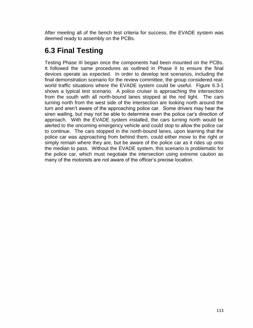
113
After meeting all of the bench test criteria for success, the EVADE system was deemed ready to assembly on the PCBs.
6.3 Final Testing
Testing Phase III began once the components had been mounted on the PCBs. It followed the same procedures as outlined in Phase II to ensure the final devices operate as expected. In order to develop test scenarios, including the final demonstration scenario for the review committee, the group considered real-world traffic situations where the EVADE system could be useful. Figure 6.3-1 shows a typical test scenario. A police cruiser is approaching the intersection from the south with all north-bound lanes stopped at the red light. The cars turning north from the west side of the intersection are looking north around the turn and aren‟t aware of the approaching police car. Some drivers may hear the siren wailing, but may not be able to determine even the police car‟s direction of approach. With the EVADE system installed, the cars turning north would be alerted to the oncoming emergency vehicle and could stop to allow the police car to continue. The cars stopped in the north-bound lanes, upon learning that the police car was approaching from behind them, could either move to the right or simply remain where they are, but be aware of the police car as it rides up onto the median to pass. Without the EVADE system, this scenario is problematic for the police car, which must negotiate the intersection using extreme caution as many of the motorists are not aware of the officer‟s precise location.
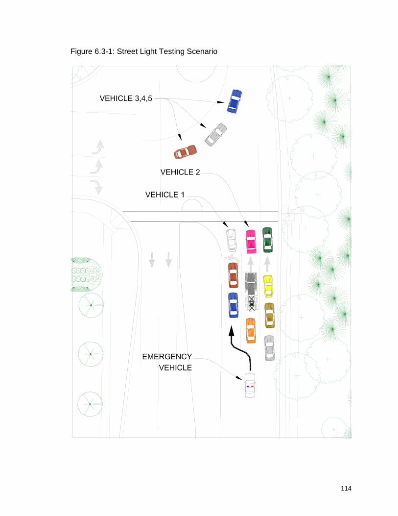
114
Figure 6.3-1: Street Light Testing Scenario

115
7. Operation Manual
The EVADE system is designed to be fully automated, with no input required from the user. Normal operation of the motor vehicle in which the system is installed will result in proper system operation.
7.1 Installation
The EVADE system is composed of two distinct devices: the Emergency Alert Transmitter (EAT) and the Emergency Alert Receiver (EAR). The EAT is a single module and is to be installed in emergency vehicles. It should be placed behind the dashboard, or in some other location where the vehicle‟s communication equipment will not interfere with the EAT‟s GPS reception, AM transmitter, or digital compass operation. The ETD within the EAT will be connected to the emergency vehicle‟s existing emergency light switch. The PCM will be connected to the 12V accessory line at or near the main fuse box.
The EAR is to be installed in non-emergency vehicles (passenger vehicles, commercial trucks, etc.). It is comprised of two modules: the main body and the VDU. Like the EAT, the main body of the EAR will be installed behind the dashboard or in some other location where the vehicle‟s electronics will not interfere with the proper operation of the EAR. The vehicle‟s front two speaker wires will be cut and installed with appropriate connectors. These connectors will then plug into the EAR. The PCM will be connected to the 12V accessory line at or near the main fuse box. The VDU will be installed in or on the dashboard so as to be visible by the driver, but not overly obtrusive.
7.2 Operation
7. 2. 1 EAT
Under normal, non-emergency conditions, the EAT will be collecting GPS and compass data, but it will not be transmitting. The device should be effectively invisible to the vehicle operator.
When the vehicle operator activates the vehicle‟s emergency lights, the EAT immediately begins transmitting. No other user action is required and no visible effect will observed.
7. 2. 2 EAR
Under normal, non-emergency conditions, the VDU will display the vehicle‟s heading (N, NE, E, SE, S, SW, W, NW). No bezel LEDs should light under normal conditions. The EAR will not affect the operation of the vehicle‟s stereo system.

116
When an emergency alert signal is detected, the EAR will bypass the stereo and begin playing the appropriate alert message through the front two speakers. At the same time, the VDU will display the corresponding visual alert as well as indicate the relative direction of the emergency vehicle via the bezel LEDs.
When the EAR no longer receives an emergency signal, it will resume its normal mode of operation.

117
8. Design Summary
The overall block diagrams for the Emergency Vehicle Alert Device are shown below. Figure 2.2.1-1 shows the block diagram for the Emergency Alert Transmitter, which will be installed on emergency vehicles.
Figure 2.2.1-1: Block Diagram of Emergency Alert Transmitter
TCU
+
_
+_
EMERGENCY VEHICLE
BATTERY
(POWER SUPPLY)
8-BIT SIGNAL
HEC
MEMORY POWER
8-B
IT
CO
MP
AS
S S
IGN
AL
TOD
PCM
(IF REQ'D)
1
3
1 3
3
D
D
J
J
1
CONNECT TO EXISTING
SWITCH THAT TURNS ON
EMERGENCY LIGHTS.
POWER
POWER
IGNITION
BLOCK LEGEND
PCM - POWER CONTROL MODULE
TOD - TURN ON DEVICE (SWITCH)
HEC - HALL EFFECT COMPASS
TCU - TRANSMITTER CONTROL UNIT
ETD - EMERGENCY TRANSMISSION DEVICE
STATUS
1 TO BE ACQUIRED
ACQUIRED
RESEARCH
DESIGN
PROTOTYPE
COMPLETED
2
3
4
5
6
DEVELOPER
CHUCK
JOSH
STEPHEN
DERRICK
C
J
S
D
ETD
3 J
J1 3
8-B
IT S
IGN
AL
8-B
IT S
IGN
AL
AUTOMOBILE
ANTENNA 1

118
The block diagram for the Emergency Alert Receiver is shown in Figure 2.2.2-1. This device will be installed on passenger vehicles and will alert the drivers to the presence of a nearby emergency vehicle.
Figure 2.2.2-1: Block Diagram of Emergency Alert Receiver
RCU
+
_
+_
AUTOMOBILE
ANTENNA
AUTOMOBILE
BATTERY
(POWER SUPPLY)
SIGNAL FROM
"EAT" SOURCE8-BIT SIGNAL
HEC
MEMORY POWER
POWER
8-B
IT
CO
MP
AS
S S
IGN
AL
TOD
PCM
(IF REQ'D)
1
1
3
3
3
3
D
D
S
J D
1
J D
POWER
IGNITION
BLOCK LEGEND
PCM - POWER CONTROL MODULE
TOD - TURN ON DEVICE (SWITCH)
HEC - HALL EFFECT COMPASS
RCU - RECEIVER CONTROL UNIT
SBU - SWITCH/BYPASS UNIT
RAA - RECORDED AUDIBLE ALERT
VDU - VISUAL DISPLAY UNIT
1 2 3 4 5 6
96.5
SP
EA
KE
R
RAAAUTOMOBILE
STEREO
AUTOMOBILE
1
SPEAKERS
1
1
AU
DIB
LE
ALE
RT
ME
SS
AG
E
C SIG
NA
L
VDU
3 C
SBU
CO
NT
RO
L S
IGN
AL
STATUS
1 TO BE ACQUIRED
ACQUIRED
RESEARCH
DESIGN
PROTOTYPE
COMPLETED
2
3
4
5
6

119
8.1 Turn-On Device
The Turn-On Device for the Emergency Alert Transmitter (EAT) consists of a simple switch. In a production version, it would be incorporated into the pre-existing light switches in the emergency vehicle. Figure 4.2.2-2 shows the TOD wired between the vehicle battery and the Emergency Transmission Device (ETD). When the TOD is off, no power flows into the ETD and the EAT does not transmit. Figure 4.2.2-2: TOD Block Diagram
The Turn-On Device for the Emergency Alert Receiver is incorporated into the Receiver Control Unit (RCU) and is realized using software programming of the TCU.
8.2 Power Control Modules
The power control modules for both the EAT and the EAR are realized using linear voltage regulators. Both take the 12 V from the vehicle power system and filter the input against noise from the alternator. Both also use filter capacitors on each output to further stabilize the output voltages. As can be seen in Figure 4.2.1-1, the PCM-EAT outputs up to 600 mA at 3.3 V. The 5V regulator serves only to step down the 12V vehicle power because the 3.3V regulators cannot handle more than 6V.

120
Figure 4.2.1-1: Final Schematic for Power Control Module
Figure 4.3.1-1 shows the layout of the PCM-EAR. The 3.3V line can source up to 1 A, but is limited by the cascade configuration with the 5V regulator to 800 mA. This is further reduced by any current drawn from the 5V line (up to 800 mA). Assuming balanced current draws, each line can source up to 400 mA. The EVADE prototype operates well below this threshold on both lines.
Figure 4.3.1-1: Final Design Schematic for Receiver Power Control Module

121
8.3 Hall-Effect Compass
The Hall-Effect Compass (HEC) Modules for both the EAT and the EAR are identical, so no distinction between the modules will be made here. The Hall-Effect Compass is capable of outputting eight different directional readings (N, E, S, W, NE, SE, SW, NW). The outputs are open collector NPN transistors which will sink 25 mA at 12 V. However, for our application, the HEC will be operated at a lower voltage level, and will therefore sink a smaller output current.
The interface protocol used to communicate between the compass and the PIC processor is the I2C protocol. The data rate between the two devices is the standard 100 kbps rate for I2C. The format of the data bytes are case sensitive ASCII characters. In order to write data to the HMC6352 the slave address is 42(hex) and to command a read operation the value of 43(hex) will be sent over the I2C line. All bus transactions will begin with the master device (dsPIC30f4013) issuing the start sequence followed by the slave (HMC6352) address byte. All the bus transactions will be terminated with the master issuing a stop sequence, the ASCII character “S”. Figure 4.2.3.1-1 shows the interface commands and responses for the HMC6352.
Figure 4.2.3.1-1: Interface Commands and Responses
Command byte ASCII
Argument 1
byte
Argument 1
byte
Response 1
byte
Response 1
byte Description
w (77) EEPROM
address Data N/A N/A Write to EEPROM
r (72) EEPROM
address N/A Data N/A Read from EEPROM
G (47) RAM
address Data N/A N/A Write to RAM Register
g (67) RAM
address N/A Data N/A Read from RAM Register
S (53) N/A N/A N/A N/A Enter Sleep Mode (Sleep)
W (57) N/A N/A N/A N/A Exit Sleep Mode (Wakeup)
O (4F) N/A N/A N/A N/A Update Bridge Offsets (S/R
Now)
C (43) N/A N/A N/A N/A Enter User Calibration Mode
E (45) N/A N/A N/A N/A Exit User Calibration Mode
L (4C) N/A N/A N/A N/A Save Op Mode to EEPROM
A (41) N/A N/A MLB Data LSB Data Get Data. Compensate and
Calculate New Heading

122
The HMC6352 contains EEPROM memory that stores operational parameters. Figure 4.2.3.1-2 shows the EEPROM locations that the user can read from or write to.
Figure 4.2.3.1-2: HMC6352 EEPROM locations
EE Address (hex) Byte Description Factory Default
00 I2C Slave Address 42(hex)
01 Magnetometer X Offset MSB factory test value
02 Magnetometer X Offset LSB factory test value
03 Magnetometer Y Offset MSB factory test value
04 Magnetometer Y Offset LSB factory test value
05 Time Delay (0 – 255 ms) 01(hex)
06 Number of Summed measurements(1-16) 04(hex)
07 Software Version Number >01(hex)
08 Operation Mode Byte 50(hex)
The HMC6352 is operated in Standby Mode; it waits to receive the command to get the compass heading and then sends the data. It will then what until another receive data command is sent to get another compass heading.
8.4 GPS Modules
The GPS Modules for both the EAT and the EAR are identical, so no distinction between the modules will be made here. The Global Sat Technology Corporation EM 408 was almost a plug in and go device. Only a few external components were needed along with the GPS module. These components were simple pull-up resistors and were used to ensure that the GPS module operates at its optimal performance level and the output can be clearly read. Figure 4.2.3.2-1 shows the wiring description for the Global Sat Technology Corporation EM 408. Figure 4.2.3.2-1: EM 408 Pin Descriptions
Pin # Name Description
1 Enable/Disable Connected to Vcc to turn on (leave low to disable)
2 Gnd Grounded to common ground for PIC and GPS
3 Rx Main receive channel for receiving software commands to the engine board from user. Since not in use, this pin must be kept high for operation.
4 Tx This is the main transmit for outputting navigation and measurement data to user‟s software.
5 Vcc Connected to 3.3V DC power supply

123
The Rx line of the GPS module was connected to a pull-up resistor, which connects the Rx line to Vcc as is standard for a UART line. The resistor is stated
to need to range from 4.7 k to 10k in order to pull the line up to the proper level without leaving it hanging or too high. As is common to TTL level communication, the UART line must be 3.3 V when pulled high, which is not an issue since we designed the transmitter to operate entirely off of 3.3V. Figure 4.2.3.2-2 shows the completed diagram of the GPS module.
Figure 4.2.3.2-2: Recommended Application Schematic
The EVADE GPS utilizes GGA message format. The message utilizes ASCII code for each letter and symbol, so each individual letter of the code is sent individually along the UART connection. The GGA message format is shown in Figure 4.2.3.2-4 along with a table showing the breakdown of the message formatting.
Figure 4.2.3.2-5: GGA Message Format
GGA Message Formatting: $GPGGA,hhmmss.sss,ddmm.mmmm,X,dddmm.mmmm,Y,1,07,1.0,9.0,M,,,,0000,*18,<CR><LF>
Name Section from Example Description
Message ID $GPGLL Standard GLL protocol heading
UTC Time hhmmss.sss Coordinated Universal Time
Latitude ddmm.mmmm Latitude Coordinates
N/S Indicator X N=North, S=South
Longitude dddmm.mmmm Longitude Coordinates
E/W Indicator Y E=East, W=West
Position Fix 1 Gives satellite fix status
Satellites Used 07 Ranges from 0 to 12
Geographical and Positional
1.0,9.0,M,,,,0000 Multiple words of unused geographic and positional data.
Checksum *18 Error checking count
<CR><LF> <CR><LF> End of message termination
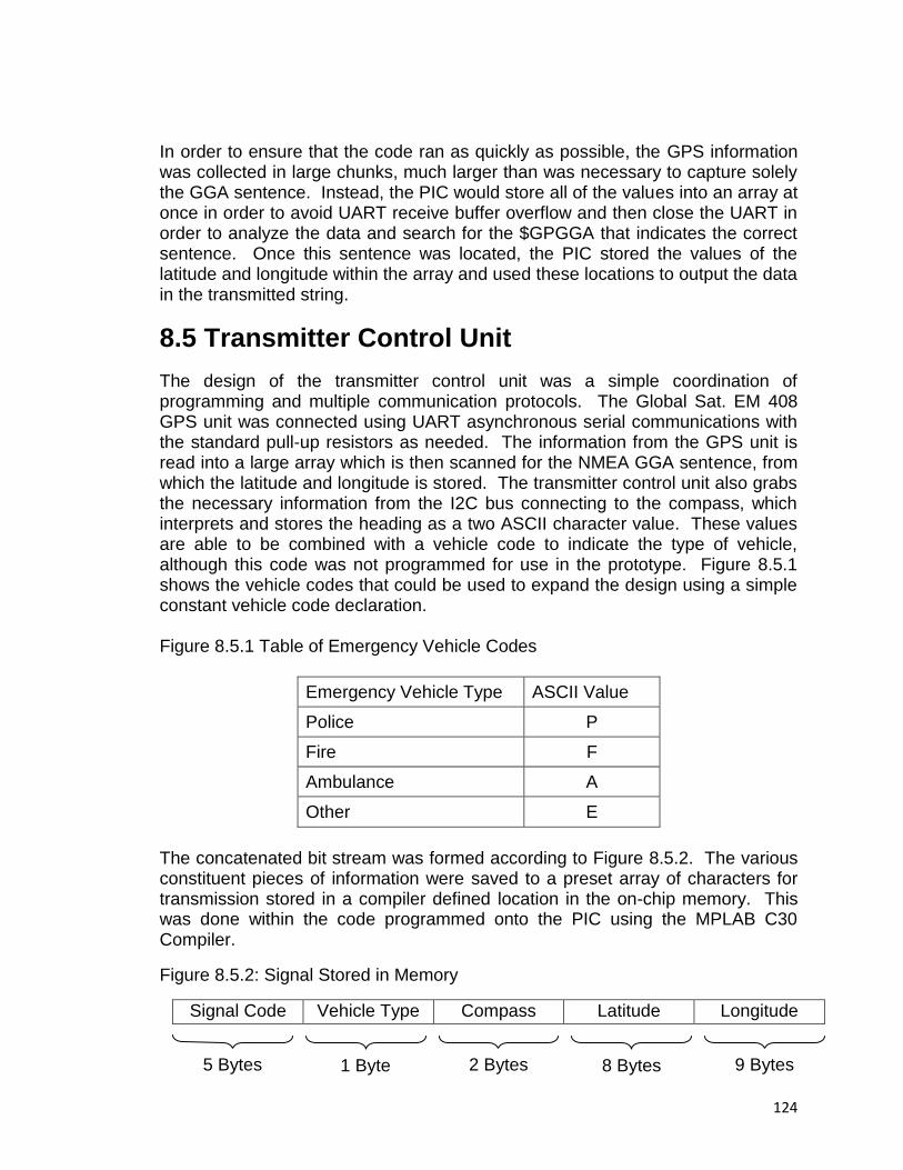
124
In order to ensure that the code ran as quickly as possible, the GPS information was collected in large chunks, much larger than was necessary to capture solely the GGA sentence. Instead, the PIC would store all of the values into an array at once in order to avoid UART receive buffer overflow and then close the UART in order to analyze the data and search for the $GPGGA that indicates the correct sentence. Once this sentence was located, the PIC stored the values of the latitude and longitude within the array and used these locations to output the data in the transmitted string.
8.5 Transmitter Control Unit
The design of the transmitter control unit was a simple coordination of programming and multiple communication protocols. The Global Sat. EM 408 GPS unit was connected using UART asynchronous serial communications with the standard pull-up resistors as needed. The information from the GPS unit is read into a large array which is then scanned for the NMEA GGA sentence, from which the latitude and longitude is stored. The transmitter control unit also grabs the necessary information from the I2C bus connecting to the compass, which interprets and stores the heading as a two ASCII character value. These values are able to be combined with a vehicle code to indicate the type of vehicle, although this code was not programmed for use in the prototype. Figure 8.5.1 shows the vehicle codes that could be used to expand the design using a simple constant vehicle code declaration. Figure 8.5.1 Table of Emergency Vehicle Codes
Emergency Vehicle Type ASCII Value
Police P
Fire F
Ambulance A
Other E
The concatenated bit stream was formed according to Figure 8.5.2. The various constituent pieces of information were saved to a preset array of characters for transmission stored in a compiler defined location in the on-chip memory. This was done within the code programmed onto the PIC using the MPLAB C30 Compiler.
Figure 8.5.2: Signal Stored in Memory
Signal Code Vehicle Type Compass Latitude Longitude
5 Bytes 1 Byte 2 Bytes 8 Bytes 9 Bytes

125
The dsPIC30F4013 takes these values and uses simple statements similar to printf in C to output these words in their proper order as stored. The register values configured in the PIC determines the UART settings such as baud rate as configured by the MPLAB compiler. These values are shifted out in order and sent to the transmitter along the data line to be modulated and broadcast wirelessly.
8.6 Transmitter, Receiver, Antenna
8.6.1 Transmitter
The Linx TXM-433-LR was the transmitter chosen for the EVADE system. Figure 4.2.4-2 shows a description of each of the transmitter‟s pins. The components that will needed to be added this transmitter will set the operating frequency of the transmitter as well as optimize the transmitter‟s performance. Figure 4.2.4-3 shows the designed layout of the TXM-433-LR.
Figure 4.2.4-2: TXM-433-LR Pin Descriptions
Pin Number Pin Name Pin Description
1 GND Ground
2 DATA Input data
3 GND Ground
4 LADJ Output power adjustment
5 ANT Output pin to antenna
6 GND Ground
7 VCC Input voltage
8 PDN Power down mode pin
Figure 4.2.4-3: Schematic of TXM-433-LR Circuit
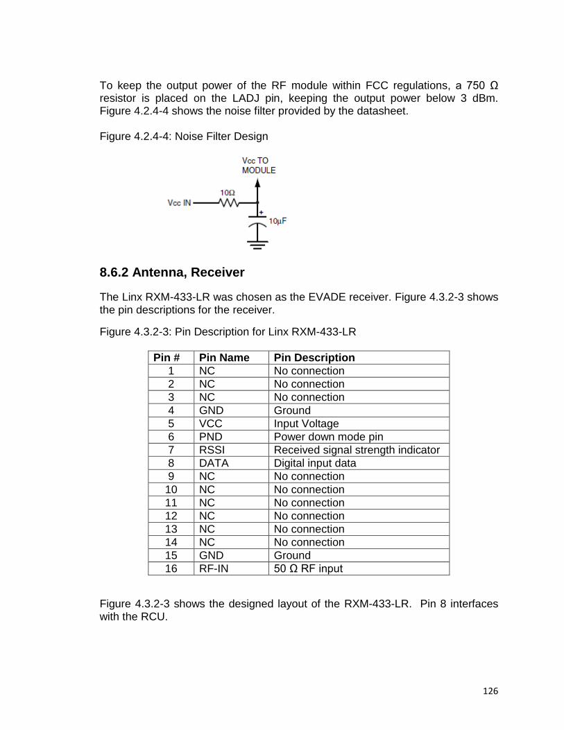
126
To keep the output power of the RF module within FCC regulations, a 750 Ω resistor is placed on the LADJ pin, keeping the output power below 3 dBm. Figure 4.2.4-4 shows the noise filter provided by the datasheet. Figure 4.2.4-4: Noise Filter Design
8.6.2 Antenna, Receiver
The Linx RXM-433-LR was chosen as the EVADE receiver. Figure 4.3.2-3 shows the pin descriptions for the receiver.
Figure 4.3.2-3: Pin Description for Linx RXM-433-LR
Pin # Pin Name Pin Description
1 NC No connection
2 NC No connection
3 NC No connection
4 GND Ground
5 VCC Input Voltage
6 PND Power down mode pin
7 RSSI Received signal strength indicator
8 DATA Digital input data
9 NC No connection
10 NC No connection
11 NC No connection
12 NC No connection
13 NC No connection
14 NC No connection
15 GND Ground
16 RF-IN 50 Ω RF input
Figure 4.3.2-3 shows the designed layout of the RXM-433-LR. Pin 8 interfaces with the RCU.

127
Figure 4.3.2-3: Schematic of Linx RX-433-LR
8.7 Receiver Control Unit
Very similar to how the original signal was read from memory and sent to the transmitter in order to be broadcast, the received signal was interfaced the same way with the receiver control unit. As the information was being collected from the reception antenna, our dsPIC30F4013 in the receiver control unit stored the signal in a pre-specified location in the on-chip memory. As described in Section 4. 2. 3, the necessary steps to correctly save the incoming signal was made very easy by the automatic memory mapping performed by the declaration of the necessary array within the code and the compilation by the MPLAB C30 compiler.
The receiver control unit also has the exact same interface with the Hall effect compass and the GPS sensor in the receiving vehicle as has been previously discussed for the transmitter control unit. This information was used to determine the heading of the vehicle in relation to the emergency vehicle broadcasting the signal. GPS measurements were taken with respect to the angle from the equator or the Prime Meridian. The latitude coordinates were given in degrees and minutes measured from the equator, which in the case of the project was the number of degrees above the equator.
Considering the receiving vehicle to be at the origin of a standard Cartesian coordinate system, we took the difference of coordinates to give the location of the emergency vehicle relative to the receiving vehicle in four quadrants. The difference of the receiving vehicle‟s coordinates minus the emergency vehicles coordinates created four possible quadrants as shown in Figure 4.3.3-1. Once the quadrant was determined, the directional headings of both compasses were considered in order to determine if it is appropriate to alert the driver.

128
Figure 4.3.3-1: Condition of Intersection as Calculated from Directional Headings
QUADRANT( + , + )
NNW
W
QUADRANT( - , + )
QUADRANT( + , - )
QUADRANT( - , - )
E
NEN
SSE
E
SWS
W
The table and diagram shown in Figure 4.3.3-1 and Figure 4.3.3-2 made the breakdown of conditions for an alert extremely simple to understand visually and easy to program using a series of if and else if statements.

129
Figure 4.3.3-2: Determined if Statements for Directional Headings
Car Direction Emergency Vehicle Direction If Statement
North If North and Quad (+,-) or Quad (+,+) -> Alert “Rear”
North If South and Quad (-,-) or Quad (-,+) -> Alert “Front”
North If East and Quad (+,-) or Quad (-,-) -> Alert “Left”
North If West and Quad (+,+) or Quad (-,+) -> Alert “Right”
South If North and Quad (+,-) or Quad (+,+) -> Alert “Front”
South If South and Quad (-,-) or Quad (-,+) -> Alert “Rear”
South If East and Quad (+,-) or Quad (-,-) -> Alert “Right”
South If West and Quad (+,+) or Quad (-,+) -> Alert “Left”
East If North and Quad (+,-) or Quad (+,+) -> Alert “Left”
East If South and Quad (-,-) or Quad (-,+) -> Alert “Right”
East If East and Quad (+,-) or Quad (-,-) -> Alert “Rear”
East If West and Quad (+,+) or Quad (-,+) -> Alert “Front”
West If North and Quad (+,-) or Quad (+,+) -> Alert “Right”
West If South and Quad (-,-) or Quad (-,+) -> Alert “Left”
West If East and Quad (+,-) or Quad (-,-) -> Alert “Front”
West If West and Quad (+,+) or Quad (-,+) -> Alert “Rear”
It can be observed from Figure 4.3.3-2 that only four main alert message groups were needed in the memory of the controller; one for the case where the emergency vehicle was approaching from the left, right, front, or rear. One case that was not shown in the table is the situation where the emergency vehicle was approaching from one of the intermediate directions, namely NE, NW, SE, or SW. Therefore, when the heading was in one of the intermediate states, the difference in latitude and longitude was compared, which allowed the control unit to determine if the approaching vehicle was closer from the front/rear or from the left/right.
8.8 Recorded Audible Alert
The Recorded Audible Alert module is implemented using a Nuvoton ISD1760 ChipCorder and an ATmega328 microcontroller. The RAA schematic, used in the final production of the PCB design files, is shown in Figure 4.3.4.1-1. This schematic also includes the SBU relays and interconnects.

130
Figure 4.3.4.1-1: RAA/SBU Schematic
The RAA receives a control signal from the RCU via pins 28, 27, and 26 (MSB → LSB) and determines which alert message to play. At the same time, if a valid alert code is output by the RCU, then the RAA microcontroller sets its pin 4 high in order to trigger the SBU.
The alert messages are stored in the ISD1760 Flash memory as wav files. They were initially recorded on a PC, then transferred to the ChipCorder via the MIC input on pins 10 and 11. The microphone was removed in order to interface the PC with the MIC pins. Utilizing this setup resulted in sufficient amplification of the audio messages, eliminating the need for an external amplifier and all of its associated components.
8.9 Visual Display Unit
Figure 4.3.4.2-1 shows a sample of possible situations that might be encountered for every directional heading and the appropriate message that should be displayed as well as the appropriate edge LED light that should be illuminated. The full table may be found in Appendix A-1.

131
Figure 4.3.4.2-1: Sample Visual Display Settings per Directional Heading
Emergency Vehicle Facing
Passenger Vehicle Facing
Emergency Vehicle
Status (per GPS)
Direction relating to passenger
vehicle/message to display
LED to
light
N S In transit EMERGENCY VEHICLE APPROACHING FROM
FRONT 1
NE S Non moving APPROACHING
EMERGENCY VEHICLE FROM FRONT
2
E S In transit EMERGENCY VEHICLE APPROACHING FROM
RIGHT 3
SE S In transit EMERGENCY VEHICLE APPROACHING FROM
REAR 4
S S In transit EMERGENCY VEHICLE APPROACHING FROM
REAR 5
SW S In transit EMERGENCY VEHICLE APPROACHING FROM
REAR 6
W S In transit EMERGENCY VEHICLE APPROACHING FROM
LEFT 7
NW S Non moving APPROACHING
EMERGENCY VEHICLE FROM FRONT
8
In order to light the eight LED lights on the edge of the display, the circuit diagram in Figure 4.3.4.2-2 was developed.

132
Figure 4.3.4.2-2: Circuit Design for LED Edge Lights
Five control lines from the RCU trigger the message to be displayed and which LED to light up. The various display messages are hard coded into the VDU‟s ATmega328P microprocessor. The LCD interfaces with the ATmega328 and includes an LCD backlight through a 33 Ohm resistor (for brightness control). The LCD display has eight parallel input pins, which correlate to the eight bit codes to light up each letter. Due to pin constraints on the ATmega 8 series chips, we chose to send the data in two 4-bit nibbles to the LCD display. With the incorporation of the integrated HD44780 display driver, the need for programming the individual hexadecimal letter codes directly to the LCD input ports became unnecessary. The Hitachi driver converts the strings sent from the microprocessor into the appropriate 8-bit letter codes and displays them to the screen. The following table is an example of the bit-code and corresponding hexadecimal code that the HD44780 converts each character into prior to sending the final information to the LCD.

133
Figure 4.3.4.2-3: Visual Display Letter Codes
8 Bit and Hexadecimal Letter Codes
0010 0000 = 20 = (space) 0100 1001 = 49 = “I” 0101 0010 = 52 = “R”
0100 0001 = 41 = “A” 0100 1010 = 4A = “J” 0101 0011 = 53 = “S”
0100 0010 = 42 = “B” 0100 1011 = 4B = “K” 0101 0100 = 54 = “T”
0100 0011 = 43 = “C” 0100 1100 = 4C = “L” 0101 0101 = 55 = “U”
0100 0100 = 44 = “D” 0100 1101 = 4D = “M” 0101 0110 = 56 = “V”
0100 0101 = 45 = “E” 0100 1110 = 4E = “N” 0101 0111 = 57 = “W”
0100 0110 = 46 = “F” 0100 1111 = 4F = “O” 0101 1000 = 58 = “X”
0100 0111= 47 = “G” 0101 0000 = 50 = “P” 0101 1001 = 59 = “Y”
0100 1000 = 48 = “H” 0101 0001 = 51 = “Q” 0101 1010 = 5A = “Z”
The messages were programmed as a line-by-line set of code so that each line displayed correctly. Then the group of four lines was grouped as a set, and then the microcontroller was used to choose the set of lines to display. The directional LED‟s around the VDU bezel are controlled by the VDU microcontroller via an 8-bit shift register (Texas Instruments SN74HC595), controlled through the SPI lines of the microprocessor. The shift register exhibits low power consumption, and ease of latching capability.
8.10 Switching Bypass Unit
The SBU is realized using 2 electromechanical bypass relays, which are controlled by an additional relay, shown below in Figure 4.3.4.1-2. The inputs are the car stereo (front) speaker lines and the RAA output. The outputs of the relays connect directly to the car speakers. The control line is connected to the RAA controller (ATmega328) which sends a logic high (3.3V) only when an emergency alert message is playing. The control relay is needed because neither the RCU nor the RAA microcontroller were able to supply the 5V necessary to engage the bypass relays.

134
Figure 4.3.4.1-2 Switching Bypass Unit Design Schematic
135
9. Summary and Conclusion
Throughout this year, the Emergency Vehicle Alert DEvice (EVADE), has presented the group with a number of challenges and learning moments. Overcoming the challenges that have been presented to the group was not an easy task. In the beginning, ambition for the project was very high and all kinds of ideas and different features for this project were considered. But as research was done to try to implement all these different ideas and features, a more basic approach to the project had to be taken. A lot of the simple aspects of the design of this project turned out not to be as simple as they first appeared. Learning how to integrate the proper components was not as easily done as it was thought to be. Getting all the operating voltages of the components to match up like it was first expected did not happen. Many different components were made by different manufacturers, so they just didn‟t operate together as expected. Some components were meant to be operated with batteries, so they used lower power to conserve energy. While it was found that other components often did not have power consumption in mind, so they operated at much higher voltages. Linear regulators had to be chosen to give the desired operating voltages that each component could be operated at. Also learning the binary information, NMEA 0183, that is generated by the GPS module could have been a 4000 level class in itself. The code that is needed to process the data is definitely more complex than any code that has been shown to the group so far. For this part it would have been nice to have a computer engineer in the group, but the group was intelligent enough to handle it. One of the group member did some in term work were they used FPGAs and microprocessors, so that help. The learning of different components has been a great learning experience for all of us. In researching this project, learning how to decipher datasheets was learned, mainly because datasheets are not something that are widely taught in the classroom. Doing the learning in a manner where one has to go research all the information on their own without being told what to study is definitely not an easy task. But, doing the research in this manner is definitely a better learning experience for an engineer than sitting in a class listening to a professor since observing what has to be done is a lot easier than having to go find out what to do on your own. This project has been a great learning experience for the whole group and we have not only learned to research things our self, but to work with each other to accomplish a single goal, completing the project.

A
A. Appendices
A-1. Visual Display Settings by Directional Heading
Figure A-1-1: North
Emergency Vehicle Facing
Passenger Vehicle Facing
Emergency Vehicle Status
(per GPS)
Direction relating to passenger vehicle/message to display
LED to light
N N In transit EMERGENCY VEHICLE
APPROACHING FROM REAR 5
N NE In transit EMERGENCY VEHICLE
APPROACHING FROM REAR 4
N E In transit EMERGENCY VEHICLE
APPROACHING FROM RIGHT 3
N SE In transit EMERGENCY VEHICLE
APPROACHING FROM FRONT 2
N S In transit EMERGENCY VEHICLE
APPROACHING FROM FRONT 1
N SW In transit EMERGENCY VEHICLE
APPROACHING FROM FRONT 8
N W In transit EMERGENCY VEHICLE
APPROACHING FROM LEFT 7
N NW In transit EMERGENCY VEHICLE
APPROACHING FROM REAR 6
N SE Non moving APPROACHING EMERGENCY
VEHICLE FROM FRONT 2
N S Non moving APPROACHING EMERGENCY
VEHICLE FROM FRONT 1
N SW Non moving APPROACHING EMERGENCY
VEHICLE FROM FRONT 8

B
Figure A-1-2: North-East
NE N In transit EMERGENCY VEHICLE
APPROACHING FROM REAR 6
NE NE In transit EMERGENCY VEHICLE
APPROACHING FROM REAR 5
NE E In transit EMERGENCY VEHICLE
APPROACHING FROM REAR 4
NE SE In transit EMERGENCY VEHICLE
APPROACHING FROM RIGHT 3
NE S In transit EMERGENCY VEHICLE
APPROACHING FROM FRONT 2
NE SW In transit EMERGENCY VEHICLE
APPROACHING FROM FRONT 1
NE W In transit EMERGENCY VEHICLE
APPROACHING FROM FRONT 8
NE NW In transit EMERGENCY VEHICLE
APPROACHING FROM LEFT 7
NE S Non moving APPROACHING EMERGENCY
VEHICLE FROM FRONT 2
NE SW Non moving APPROACHING EMERGENCY
VEHICLE FROM FRONT 1
NE W Non moving APPROACHING EMERGENCY
VEHICLE FROM FRONT 8
Figure A-1-3: East
E N In transit EMERGENCY VEHICLE
APPROACHING FROM LEFT 7
E NE In transit EMERGENCY VEHICLE
APPROACHING FROM REAR 6
E E In transit EMERGENCY VEHICLE
APPROACHING FROM REAR 5
E SE In transit EMERGENCY VEHICLE
APPROACHING FROM REAR 4
E S In transit EMERGENCY VEHICLE
APPROACHING FROM RIGHT 3
E SW In transit EMERGENCY VEHICLE
APPROACHING FROM FRONT 2
E W In transit EMERGENCY VEHICLE
APPROACHING FROM FRONT 1
E NW In transit EMERGENCY VEHICLE
APPROACHING FROM FRONT 8
E SW Non moving APPROACHING EMERGENCY
VEHICLE FROM FRONT 2
E W Non moving APPROACHING EMERGENCY
VEHICLE FROM FRONT 1
E NW Non moving APPROACHING EMERGENCY
VEHICLE FROM FRONT 8

C
Figure A-1-4: South-East
SE N In transit EMERGENCY VEHICLE
APPROACHING FROM FRONT 8
SE NE In transit EMERGENCY VEHICLE
APPROACHING FROM LEFT 7
SE E In transit EMERGENCY VEHICLE
APPROACHING FROM REAR 6
SE SE In transit EMERGENCY VEHICLE
APPROACHING FROM REAR 5
SE S In transit EMERGENCY VEHICLE
APPROACHING FROM REAR 4
SE SW In transit EMERGENCY VEHICLE
APPROACHING FROM RIGHT 3
SE W In transit EMERGENCY VEHICLE
APPROACHING FROM FRONT 2
SE NW In transit EMERGENCY VEHICLE
APPROACHING FROM FRONT 1
SE W Non moving APPROACHING EMERGENCY
VEHICLE FROM FRONT 2
SE NW Non moving APPROACHING EMERGENCY
VEHICLE FROM FRONT 1
SE N Non moving APPROACHING EMERGENCY
VEHICLE FROM FRONT 8
Figure A-1-5: South
S N In transit EMERGENCY VEHICLE
APPROACHING FROM FRONT 1
S NE In transit EMERGENCY VEHICLE
APPROACHING FROM FRONT 8
S E In transit EMERGENCY VEHICLE
APPROACHING FROM LEFT 7
S SE In transit EMERGENCY VEHICLE
APPROACHING FROM REAR 6
S S In transit EMERGENCY VEHICLE
APPROACHING FROM REAR 5
S SW In transit EMERGENCY VEHICLE
APPROACHING FROM REAR 4
S W In transit EMERGENCY VEHICLE
APPROACHING FROM RIGHT 3
S NW In transit EMERGENCY VEHICLE
APPROACHING FROM FRONT 2
S NW Non moving APPROACHING EMERGENCY
VEHICLE FROM FRONT 2
S N Non moving APPROACHING EMERGENCY
VEHICLE FROM FRONT 1
S NE Non moving APPROACHING EMERGENCY
VEHICLE FROM FRONT 8

D
Figure A-1-6: South-West
SW N In transit EMERGENCY VEHICLE
APPROACHING FROM FRONT 2
SW NE In transit EMERGENCY VEHICLE
APPROACHING FROM FRONT 1
SW E In transit EMERGENCY VEHICLE
APPROACHING FROM FRONT 8
SW SE In transit EMERGENCY VEHICLE
APPROACHING FROM LEFT 7
SW S In transit EMERGENCY VEHICLE
APPROACHING FROM REAR 6
SW SW In transit EMERGENCY VEHICLE
APPROACHING FROM REAR 5
SW W In transit EMERGENCY VEHICLE
APPROACHING FROM REAR 4
SW NW In transit EMERGENCY VEHICLE
APPROACHING FROM RIGHT 3
SW N Non moving APPROACHING EMERGENCY
VEHICLE FROM FRONT 2
SW NE Non moving APPROACHING EMERGENCY
VEHICLE FROM FRONT 1
SW E Non moving APPROACHING EMERGENCY
VEHICLE FROM FRONT 8
Figure A-1-7: West
W N In transit EMERGENCY VEHICLE
APPROACHING FROM RIGHT 3
W NE In transit EMERGENCY VEHICLE
APPROACHING FROM FRONT 2
W E In transit EMERGENCY VEHICLE
APPROACHING FROM FRONT 1
W SE In transit EMERGENCY VEHICLE
APPROACHING FROM FRONT 8
W S In transit EMERGENCY VEHICLE
APPROACHING FROM LEFT 7
W SW In transit EMERGENCY VEHICLE
APPROACHING FROM REAR 6
W W In transit EMERGENCY VEHICLE
APPROACHING FROM REAR 5
W NW In transit EMERGENCY VEHICLE
APPROACHING FROM REAR 4
W NE Non moving APPROACHING EMERGENCY
VEHICLE FROM FRONT 2
W E Non moving APPROACHING EMERGENCY
VEHICLE FROM FRONT 1
W SE Non moving APPROACHING EMERGENCY
VEHICLE FROM FRONT 8

E
Figure A-1-8 North-West
NW N In transit EMERGENCY VEHICLE
APPROACHING FROM REAR 4
NW NE In transit EMERGENCY VEHICLE
APPROACHING FROM LEFT 3
NW E In transit EMERGENCY VEHICLE
APPROACHING FROM FRONT 2
NW SE In transit EMERGENCY VEHICLE
APPROACHING FROM FRONT 1
NW S In transit EMERGENCY VEHICLE
APPROACHING FROM FRONT 8
NW SW In transit EMERGENCY VEHICLE
APPROACHING FROM RIGHT 7
NW W In transit EMERGENCY VEHICLE
APPROACHING FROM REAR 6
NW NW In transit EMERGENCY VEHICLE
APPROACHING FROM REAR 5
NW E Non moving APPROACHING EMERGENCY
VEHICLE FROM FRONT 2
NW SE Non moving APPROACHING EMERGENCY
VEHICLE FROM FRONT 1
NW S Non moving APPROACHING EMERGENCY
VEHICLE FROM FRONT 8
A-2. Works Consulted
1.) Antoniou, Andreas. Digital Signal Processing: Signals, Systems, and Filters. New York: McGraw-Hill, 2006. Print.
2.) Lathi, B.P. and Zhi Ding. Modern Digital and Analog Communication Systems,
Fourth Edition. New York: Oxford University Press, 2009. Print. 3.) Neamen, Donald. Microelectronics: Circuit Analysis and Design, Third Edition.
New York: McGraw-Hill, 2007. Print. 4.)Wikipedia contributors. "Voltage regulator." Wikipedia, The Free Encyclopedia.
Wikipedia, The Free Encyclopedia, 24 Apr. 2010. Web. 2 May. 2010. http://en.wikipedia.org/wiki/Voltage_stabilizer
5.) Wikipedia contributors. "Buck converter." Wikipedia, The Free Encyclopedia.
Wikipedia, The Free Encyclopedia, 13 Mar. 2010. Web. 2 May. 2010. http://en.wikipedia.org/wiki/Buck_converter
6.) Wikipedia contributors. "Switched-mode power supply." Wikipedia, The Free
Encyclopedia. Wikipedia, The Free Encyclopedia, 20 Apr. 2010. Web. 2 May. 2010. http://en.wikipedia.org/wiki/Switched-mode_power_supply

F
7.) National Archives and Records Administration. “Code of Federal
Regulations”. April 5, 2010. May 1, 2010. http://www.access.gpo.gov/cgi-bin/cfrassemble.cgi?title=200947
8.) National Archives and Records Administration. “E-code of Federal
Regulations”. April 29, 2010. May 1, 2010. http://ecfr.gpoaccess.gov/cgi/t/text/text-idx?&c=ecfr&tpl=/ecfrbrowse/Title47/47tab_02.tpl
9.) Federal Communications Commission. “FCC. Public Notice DA 96-2040.”
Dec 9, 1996. “FCC. Public Notice 14089”. Jul 24, 1991. May 1, 2010. www.fcc.gov
10.) KNJN LLC. “LED Displays” & “RS-232”. July 8, 2009. May1, 2010.
http://www.fpga4fun.com/SiteInformation.html 11.) Atmel. “AT40K05AL”, “ATK10AL”, ”AT40K20AL”, “AT40K40AL”. Copyright
2010. May 1, 2010. http://www.atmel.com/dyn/products/devices.asp?family_id=623
12.) XILINX. “Spartan-6 Family Overview”, “Spartan-6 Data Sheet : DC and
Switching Characteristics”, “Spartan-6 FPGA Clocking Resources User Guide”, “Spartan-6 FPGA Transceivers User Guide”, “Spartan-6 FPGA PCB Design and Pin Planning Design”, “Spartan-6 FPGA Configuration User Guide”, “Spartan-6 FPGA SelectIO Reseources User Guide”. http://www.xilinx.com/support/documentation/spartan-6.htm
13.) Altera. “Cyclone II Overview”, Cyclone II Design Utilities”, “Cyclone II
Features”. Copyright 2010. May 1, 2010. http://www.altera.com/products/devices/cyclone2/cy2-index.jsp
14.) Rensselaer Polytechnic Institute. “Rage Against the AVR -> (Stereo PWM
Audio)” Dane Kouttron. May 1, 2010 http://www.rpi.edu/~kouttd/03/Rage_against_the_arduino.html
15.) Wikipedia contributors. "Pulse-width modulation." Wikipedia, The Free
Encyclopedia. Wikipedia, The Free Encyclopedia, 20 Apr. 2010. Web. 2 May. 2010 http://en.wikipedia.org/w/index.php?title=Special:Cite&page=Pulse-width_modulation&id=357264791
16.) Micrel. “MICRF112 Data Sheet”, “MICRF113 Data Sheet”, “MICRF405 Data
Sheet”. Copyright 2010. May 1, 2010. http://www.micrel.com/page.do?page=product-info/qwikradio.shtml

G
17.) LUMEX. “LCM-X01604DXX Data Sheet”. October 9, 1998. May 1, 2010. http://search.digikey.com/scripts/DkSearch/dksus.dll?Detail&name=67-1761-ND
18.) Wikipedia contributors. "HD44780 Character LCD.", “Hitachi HD44780U
(LCD-II) Datasheet” Wikipedia, The Free Encyclopedia. Wikipedia, The Free Encyclopedia, 18 Apr. 2010. Web. 2 May. 2010. http://en.wikipedia.org/wiki/HD44780_Character_LCD
19.) The Robson Company, Inc. “Dinsmore Sensing Systems General
Information” May 1, 2010. http://www.robsonco.com/Dinsmore/Untitled_4.html
20.) Orcam “GPS36 SiRFstar III based OEM-GPS receiver” May 1, 2010.
http://www.orcam.eu/GPS36SiRFstarIIIbasedOEMGPSreceiver.htm 21.) Modulstek “Ultra High Sensitivity SiRFstar III 7989 GPS Module with
Miniature Dimension”. May 1, 2010. http://www.modulestek.com/DOC/SSF1513%20GPS%20Module%20Spec%20V1.0.pdf
22.) Antenova. “GPS Radionova M10214 RF Antenna Module” Copyright 2008.
May 1, 2010. http://www.antenova.com/?id=1036 23.) SiRF. “SiRF Binary Protocol Reference Manual”, Revision 2.4, November
2008. “NMEA Reference Manual”. Revision 2.1, December 2007. May 1, 2010. http://www.navmanwirelessoem.com/assets/files/Docs/SiRF%20Binary%20Protocol%20Reference%20ManualR2.4.pdf
24.) Microchip. “PIC32 Overview Brochure” November 17, 2009
“PIC32MX3XX/4XX Family Data Sheet”. April 19, 2010. http://www.microchip.com/stellent/idcplg?IdcService=SS_GET_PAGE&nodeId=2591
25.) Wikipedia contributors. "PIC microcontroller." Wikipedia, The Free
Encyclopedia. Wikipedia, The Free Encyclopedia, 2 May. 2010. Web. 2 May. 2010. http://en.wikipedia.org/wiki/PIC_microcontroller
26.) Rabbit. “Rabbit 4000 Microprocessors” Copyright 2010. May 1, 2010.
http://www.rabbit.com/products/rab4000/ 27.) “Volume IV – Digital > Serial-in, Parallel-out Shift Registers” May 1, 2010.
http://www.allaboutcircuits.com/vol_4/chpt_12/4.html
H
28.) Skyworks. “SKY65116: 390-500 MHz Linear Power Amplifier” Feb. 18, 2009. May 1, 2010. http://www.skyworksinc.com/Product.aspx?ProductID=352
29.) RF Micro Device. “XD010-EVAL_Datasheet”, Copyright 2003, May 1, 2010.
https://estore.rfmd.com/RFMD_Onlinestore/Products/RFMD+Parts/PID-P_XD010-EVAL.aspx
30.) 3M. “Opticom Priority Control System”. May 1, 2010.
http://www.yaakoby.com/Editor/assets/mediawebserver.pdf 31.) University of Central Florida, Senior Design Website
http://eecs.ucf.edu/seniordesign/ 32.) Wikipedia contributors. "Gerber File." Wikipedia, The Free Encyclopedia.
Wikipedia, The Free Encyclopedia, 23 Apr. 2010. Web. 2 May. 2010. http://en.wikipedia.org/wiki/Gerber_File
33.) Gerber System Corporation. “Gerber RS-274X Format User Guide”. May 1,
2010. http://ohm.bu.edu/~hazen/my_d0/std/rs274xc.pdf
A-3. Permissions
1.) Micrel

I
2.) Antenova
3.) www.fleetsafety.com – Still Pending
4.) www.allaboutcircuits.com
DESIGN SCIENCE LICENSE
Copyright © 1999-2000 Michael Stutz [email protected]
Verbatim copying of this document is permitted, in any medium.
0. Preamble

J
Copyright law gives certain exclusive rights to the author of a work, including the rights to copy, modify and distribute the work (the "reproductive," "adaptative," and "distribution" rights). The idea of "copyleft" is to willfully revoke the exclusivity of those rights under certain terms and conditions, so that anyone can copy and distribute the work or properly attributed derivative works, while all copies remain under the same terms and conditions as the original. The intent of this license is to be a general "copyleft" that can be applied to any kind of work that has protection under copyright. This license states those certain conditions under which a work published under its terms may be copied, distributed, and modified. Whereas "design science" is a strategy for the development of artifacts as a way to reform the environment (not people) and subsequently improve the universal standard of living, this Design Science License was written and deployed as a strategy for promoting the progress of science and art through reform of the environment.
1. Definitions "License" shall mean this Design Science License. The License applies to any work which contains a notice placed by the work's copyright holder stating that it is published under the terms of this Design Science License. "Work" shall mean such an aforementioned work. The License also applies to the output of the Work, only if said output constitutes a "derivative work" of the licensed Work as defined by copyright law. "Object Form" shall mean an executable or performable form of the Work, being an embodiment of the Work in some tangible medium. "Source Data" shall mean the origin of the Object Form, being the entire, machine-readable, preferred form of the Work for copying and for human modification (usually the language, encoding or format in which composed or recorded by the Author); plus any accompanying files, scripts or other data necessary for installation, configuration or compilation of the Work. (Examples of "Source Data" include, but are not limited to, the following: if the Work is an image file composed and edited in 'PNG' format, then the original PNG source file is the Source Data; if the Work is an MPEG 1.0 layer 3 digital audio recording made from a 'WAV' format audio file recording of an analog source, then the original WAV file is the Source Data; if the Work was composed as an unformatted plaintext file, then that file is the the Source Data; if the Work was composed in LaTeX, the LaTeX file(s) and any image files and/or custom macros necessary for compilation constitute the Source Data.) "Author" shall mean the copyright holder(s) of the Work. The individual licensees are referred to as "you."
2. Rights and copyright The Work is copyright the Author. All rights to the Work are reserved by the Author, except as specifically described below. This License describes the terms

K
and conditions under which the Author permits you to copy, distribute and modify copies of the Work. In addition, you may refer to the Work, talk about it, and (as dictated by "fair use") quote from it, just as you would any copyrighted material under copyright law. Your right to operate, perform, read or otherwise interpret and/or execute the Work is unrestricted; however, you do so at your own risk, because the Work comes WITHOUT ANY WARRANTY -- see Section 7 ("NO WARRANTY") below.
3. Copying and distribution Permission is granted to distribute, publish or otherwise present verbatim copies of the entire Source Data of the Work, in any medium, provided that full copyright notice and disclaimer of warranty, where applicable, is conspicuously published on all copies, and a copy of this License is distributed along with the Work. Permission is granted to distribute, publish or otherwise present copies of the Object Form of the Work, in any medium, under the terms for distribution of Source Data above and also provided that one of the following additional conditions are met: (a) The Source Data is included in the same distribution, distributed under the terms of this License; or (b) A written offer is included with the distribution, valid for at least three years or for as long as the distribution is in print (whichever is longer), with a publicly-accessible address (such as a URL on the Internet) where, for a charge not greater than transportation and media costs, anyone may receive a copy of the Source Data of the Work distributed according to the section above; or (c) A third party's written offer for obtaining the Source Data at no cost, as described in paragraph (b) above, is included with the distribution. This option is valid only if you are a non-commercial party, and only if you received the Object Form of the Work along with such an offer. You may copy and distribute the Work either gratis or for a fee, and if desired, you may offer warranty protection for the Work. The aggregation of the Work with other works which are not based on the Work -- such as but not limited to inclusion in a publication, broadcast, compilation, or other media -- does not bring the other works in the scope of the License; nor does such aggregation void the terms of the License for the Work.
4. Modification Permission is granted to modify or sample from a copy of the Work, producing a derivative work, and to distribute the derivative work under the terms described in the section for distribution above, provided that the following terms are met: (a) The new, derivative work is published under the terms of this License. (b) The derivative work is given a new name, so that its name or title can not be confused with the Work, or with a version of the Work, in any way. (c) Appropriate authorship credit is given: for the differences between the Work and the new derivative work, authorship is attributed to you, while the material sampled or used from the Work remains attributed to the original Author;
L
appropriate notice must be included with the new work indicating the nature and the dates of any modifications of the Work made by you.
5. No restrictions You may not impose any further restrictions on the Work or any of its derivative works beyond those restrictions described in this License.
6. Acceptance Copying, distributing or modifying the Work (including but not limited to sampling from the Work in a new work) indicates acceptance of these terms. If you do not follow the terms of this License, any rights granted to you by the License are null and void. The copying, distribution or modification of the Work outside of the terms described in this License is expressly prohibited by law. If for any reason, conditions are imposed on you that forbid you to fulfill the conditions of this License, you may not copy, distribute or modify the Work at all. If any part of this License is found to be in conflict with the law, that part shall be interpreted in its broadest meaning consistent with the law, and no other parts of the License shall be affected.
7. No warranty THE WORK IS PROVIDED "AS IS," AND COMES WITH ABSOLUTELY NO WARRANTY, EXPRESS OR IMPLIED, TO THE EXTENT PERMITTED BY APPLICABLE LAW, INCLUDING BUT NOT LIMITED TO THE IMPLIED WARRANTIES OF MERCHANTABILITY OR FITNESS FOR A PARTICULAR PURPOSE.
8. Disclaimer of liability IN NO EVENT SHALL THE AUTHOR OR CONTRIBUTORS BE LIABLE FOR ANY DIRECT, INDIRECT, INCIDENTAL, SPECIAL, EXEMPLARY, OR CONSEQUENTIAL DAMAGES (INCLUDING, BUT NOT LIMITED TO, PROCUREMENT OF SUBSTITUTE GOODS OR SERVICES; LOSS OF USE, DATA, OR PROFITS; OR BUSINESS INTERRUPTION) HOWEVER CAUSED AND ON ANY THEORY OF LIABILITY, WHETHER IN CONTRACT, STRICT LIABILITY, OR TORT (INCLUDING NEGLIGENCE OR OTHERWISE) ARISING IN ANY WAY OUT OF THE USE OF THIS WORK, EVEN IF ADVISED OF THE POSSIBILITY OF SUCH DAMAGE. END OF TERMS AND CONDITIONS