University of Brasília Institute of Physics Master’s ...
65
University of Brasília Institute of Physics Master’s Dissertation Structural and Electronic Properties of the Cove-type Graphene Nanoribbons Tiago de Sousa Araújo Cassiano Advisor: Prof. Pedro Henrique de Oliveira Neto
Transcript of University of Brasília Institute of Physics Master’s ...
University of Brasília
Institute of Physics
Master’s Dissertation
Structural and Electronic Properties of the
Cove-type Graphene Nanoribbons
Tiago de Sousa Araújo Cassiano
Advisor: Prof. Pedro Henrique de Oliveira Neto
Tiago de Sousa Araújo Cassiano
Structural and Electronic Properties of the Cove-type
Graphene Nanoribbons
Master’s Dissertation presented to the Institute
of Physics of the University of Brasília as a par-
tial requirement to obtain the Master title
Advisor: Prof. Pedro Henrique de Oliveira Neto
Brasilia, July of 2021.

"I may not believe in myself, but I believe in
what I’m doing."
James Patrick Page
Acknowledgements
To my mother, Lucenira de Sousa Araújo, and my aunt, Maria das Graças Aureliano,
for their continuous support, caring, and understanding. This work would not be possible with-
out you two. Thanks for, even not knowing what I do, still believe in my effort.
To Larissa dos Santos Born, for being an immeasurable source of kindness, compan-
ionship, and joy. Thanks for daily softening all the difficulties and intensifying all the achieve-
ments.
To all the incredible teachers which I had the pleasure to be guided by during this
period. My advisor, Pedro Henrique Oliveira Neto, for the endless effort in tutoring and develop
my scientific and personal formation. Professor Geraldo Magela, for the exciting lectures, the
patience, and the rich discussions. Professor Ricardo Gargano, for the pleasant encounters and
conversations.
To the members of my group. Dr. Leonardo Evaristo de Sousa, for the guidance, the
tolerance, and the enthusiasm in our endeavors. Fernando Teixeira Bueno, and Israel Siqueira,
for the funny discussions and friendship. To Jacyara Flores Arbues Carneiro, my office neigh-
bor. To them, and to those who were not mentioned, thank you for the laughter, work, and
frustration shared.
To all my friends, from the institute or not, thank you for the support and the moments
of joy and work shared.
University of Brasília p. iv
Resumo
Nos últimos anos, o grafeno vem promovendo inúmeros avanços tecnológicos e cien-
tíficos. Entretanto, o material não apresenta um valor de bandgap diferente de zero. Por isso,
a aplicação de grafeno puro em dispositivos semicondutores é inviável. Uma possível alterna-
tiva reside na produção de nanofitas de grafeno, ou graphene nanoribbons (GNR) em inglês.
Nesse sentido, um estudo recente descreve a síntese de uma geometria inédita de GNR. Con-
hecida como, cove-type GNR, ou CGNR, essa molécula apresenta diversas propriedades em sua
síntese que indicam um potencial uso em produção industrial. Todavia, pouco se sabe das po-
tencialidades em conduzir mudanças em sua rede. Neste trabalho, investigamos as propriedades
estruturais e eletrônicas ao conduzir dois tipos de transformações: aumento de largura e vari-
ação da distância entre os anéis de borda (λ). O estudo será feito através de simulações com-
putacionais com base no modelo Su-Schrieffer-Heeger (SSH) bi-dimensional estendido, com
acoplamento elétron-fónon. Resultados mostram que o CGNR permite uma calibração suave
e monotônica no gap, seja mudando a sua largura, ou λ. Tal propriedade, não observada em
nanofitas ordinárias até então, indica um potêncial latente superior. O trabalho também aborda
as caracteristicas das redes associadas com cada transformação. Os resultados mostram que o
CGNR é um forte candidato a ser tornar um material base na optoeletrônica no futuro.
University of Brasília p. v
Abstract
Over the past years, graphene is driving numerous theoretical and technological break-
throughs. However, it presents no bandgap. Because of that, the use of graphene in semicon-
ductor applications is diminished. An alternative is to rely on the so-called graphene nanorib-
bons (GNRs). In that sense, a recent study described a new GNR type, known as cove-type
GNR (CGNR), with a synthesis route suitable for large-scale production. Still, little is known
about the potential in modifying CGNR’s lattice. In this work, we investigated the structural
and electronic properties in change the CGNR lattice by two transformations: changes in the
width and the distance between the uppermost rings in the edge (λ). The study will unravel
through computational simulations using the 2-D extended Su-Schrieffer-Heeger (SSH) model
with electron-phonon constant. Results show that the CGNR can endure a monotonic gap decay
tuning process by varying the width or λ. Such attribute was not observable in other GNRs so
far. This study also discusses the lattice’s characteristics associated with each transformation.
In conclusion, the results show that the CGNR is a strong candidate to become a fundamental
material in future optoelectronics.
University of Brasília p. vi
CONTENTS
1 Introduction 9
1.1 Graphene . . . . . . . . . . . . . . . . . . . . . . . . . . . . . . . . . . . . . 9
1.2 Graphene nanoribbons (GNRs) . . . . . . . . . . . . . . . . . . . . . . . . . . 10
1.3 Applicability of GNRs . . . . . . . . . . . . . . . . . . . . . . . . . . . . . . 14
1.4 Objective . . . . . . . . . . . . . . . . . . . . . . . . . . . . . . . . . . . . . 16
2 Theoretical Modeling 17
2.1 1-D Generalized Hamiltonian for a Chain via SSH model . . . . . . . . . . . . 18
2.2 Generalization for 2-D Systems . . . . . . . . . . . . . . . . . . . . . . . . . . 27
3 Edge Engineering in Cove-type Graphene Nanoribbons 29
3.1 The Problem . . . . . . . . . . . . . . . . . . . . . . . . . . . . . . . . . . . . 29
3.2 Results . . . . . . . . . . . . . . . . . . . . . . . . . . . . . . . . . . . . . . . 32
3.3 Conclusion . . . . . . . . . . . . . . . . . . . . . . . . . . . . . . . . . . . . 42
vii

4 Published article (RSC ADVANCES) 44
Bibliography 52
University of Brasília p. viii
CHAPTER 1
INTRODUCTION
1.1 Graphene
Since its isolation in 2004 [1], graphene is displaying boundless potential in materials
science. Much of the attention regarding this one-atom-thick carbon allotrope lies on its unique
physicochemical properties [2, 3]. Among other facets, its mechanical, optical, and thermal
[4, 5] responses have special relevance. Unlike many other organic materials, graphene is able
to endure intense mechanical stress [6] while being extremely light-weighted. In addition, this
transparent material [7, 8] can efficiently conduct heat at wide temperature regimes [9]. Besides,
the electronic properties are even more promising. Unlike any other material in nature, graphene
presents a linear band structure [10]. This attribute allows, at least theoretically, massless charge
carriers. As a consequence, charge transport in graphene is incredibly favored. This material
can potentially change fundamental aspects of our society and current state technology.
Compared with other carbon allotropes, graphene-oriented research is relatively new.
Regardless, its applicability already branches many fields. Currently, there are reports of engi-
9
neering efforts based on its mechanical proprieties [11, 12], the development of sensing devices
[13], biomedical solutions [14], and especially electronic apparatus [15, 16, 17].
Besides all prospects, graphene is a semi-metal, having no bandgap [10]. This property
greatly limits its use in nanoelectronics. Currently, there are several techniques focused on
opening the gap. Among them, two procedures have special relevance. The doping approach
[18] consists of inserting non-carbon atoms in the lattice. This structural change enforces a
symmetry break, giving rise to a non-zero gap. In most cases, the elements chosen are oxygen,
nitrogen, or boron. The inclusion of each doping constituent can tailor the material towards
specific applications [19]. At this moment, doping is promoting the development of diverse
applications in electrochemical energy storage [20, 21], gas and optical sensing [22, 23], and
photovoltaics [24]. However, the strategy bears limitations. Some syntheses rely on the grafting
process, which inevitably depletes the mobility [25].
1.2 Graphene nanoribbons (GNRs)
The electronic confinement offers a more elegant way to open the gap by shaping the
lattice into nanoribbons. The so-called graphene nanoribbons (GNRs) [26, 27, 28] are quasi-
one-dimensional nanoestructures that provide a strong alternative for future optoelectronics.
Being a derivative of graphene, GNRs share many characteristics with its parent-material [29].
Among others, the nanoribbons present high mechanical strength [30], high charge mobility
[31, 32] and favorable thermal properties [33]. Besides, GNRs have an ultrahigh surface area
[34, 29] and the possibility of tuning its electronic properties [35, 36, 37]. The latter attribute
University of Brasília p. 10
allows highly customized materials, opening a wide range of design possibilities as well as
applicability.
1.2.1 Some Types
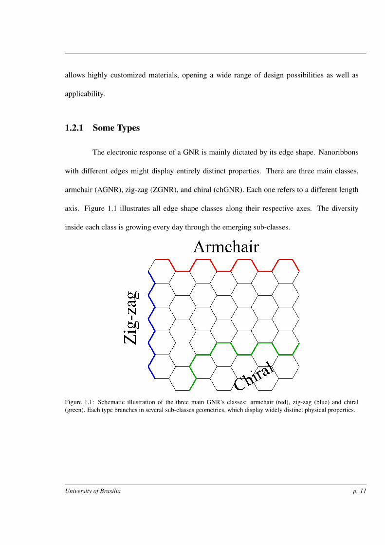
The electronic response of a GNR is mainly dictated by its edge shape. Nanoribbons
with different edges might display entirely distinct properties. There are three main classes,
armchair (AGNR), zig-zag (ZGNR), and chiral (chGNR). Each one refers to a different length
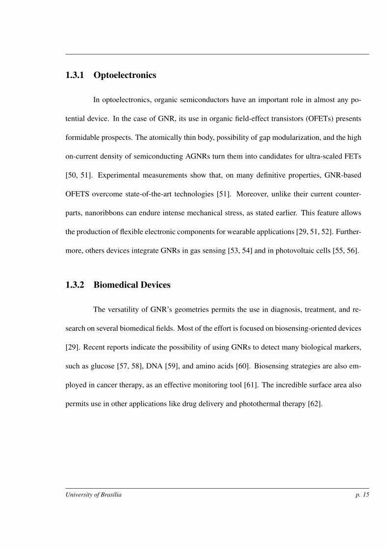
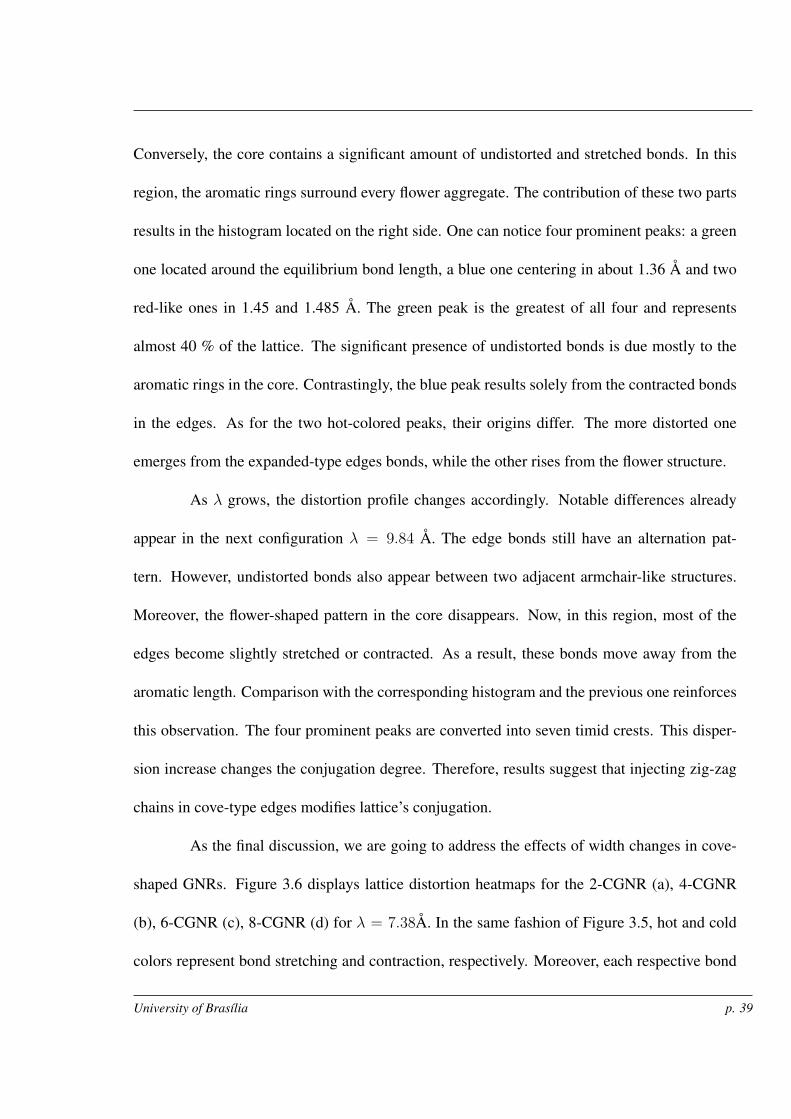
axis. Figure 1.1 illustrates all edge shape classes along their respective axes. The diversity
inside each class is growing every day through the emerging sub-classes.
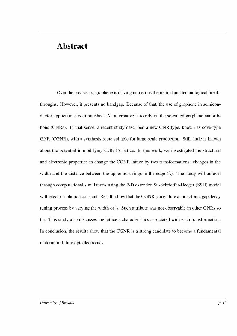
Figure 1.1: Schematic illustration of the three main GNR’s classes: armchair (red), zig-zag (blue) and chiral(green). Each type branches in several sub-classes geometries, which display widely distinct physical properties.
University of Brasília p. 11
Armchair Graphene Nanoribbons (AGNRs)
The armchair class is a type of GNR with edges resembling an armchair. It is one
of the first synthesized GNRs. Currently, most of the effort concentrates on investigating this
nanoribbon. Its pure form has three width families, 3N, 3N+1, and 3N+2, where N is the number
of sites along the width axis [26, 28]. AGNRs that belong to families 3N and 3N+1 have an
appreciable gap. Inversely, the specimens in the 3N+2 family behave as semi-metals. By far,
the AGNR type is the one with the most number of sub-classes. Here we mention the chevron
[38, 39], and the heterojunctions [40].
Zig-zag Graphene Nanoribbons (ZGNRs)
Unlike AGNRs, pure zig-zag nanoribbons do not group up in width families. Regard-
less of the width size, these materials behave as semi-metals. Although this attribute diminishes
the applicability in optoelectronics, ZGNRs have an important role in others fields, such as
spintronics [41, 42]. However, it is worth mention that, just like in graphene, doping ZGNRs
allows its use in semiconducting applications [43].
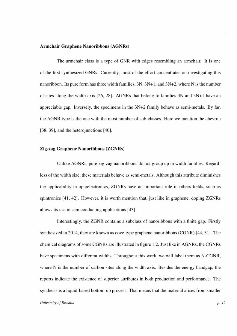
Interestingly, the ZGNR contains a subclass of nanoribbons with a finite gap. Firstly
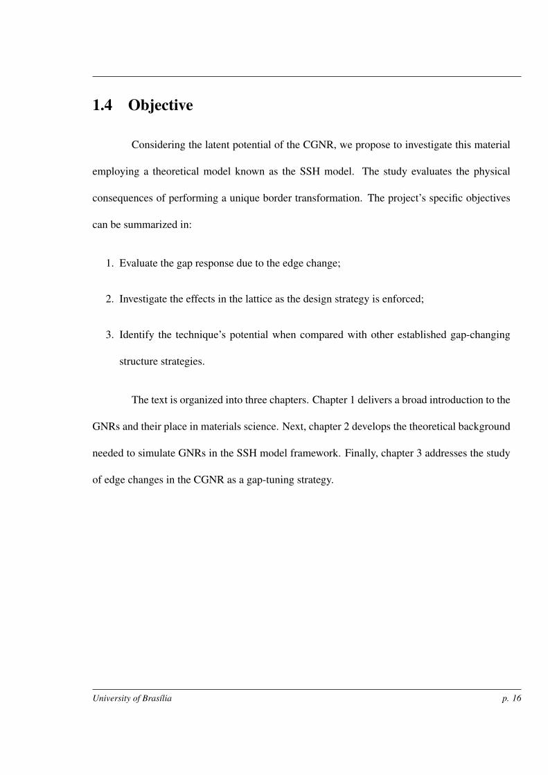
synthesized in 2014, they are known as cove-type graphene nanoribbons (CGNR) [44, 31]. The
chemical diagrams of some CGNRs are illustrated in figure 1.2. Just like in AGNRs, the CGNRs
have specimens with different widths. Throughout this work, we will label them as N-CGNR,
where N is the number of carbon sites along the width axis. Besides the energy bandgap, the
reports indicate the existence of superior attributes in both production and performance. The
synthesis is a liquid-based bottom-up process. That means that the material arises from smaller
University of Brasília p. 12
chemical precursors and supports large-scale production. Consequently, the specimens have
almost no defects. Besides the high quality, the nanoribbon is unusually long, extending up
to 200 nm. All these attributes strengthen the potential of this sub-class. Therefore, studying
such material can impact both theoretical and technological fields of low-dimensional organic
semiconductors.
Figure 1.2: Chemical diagram of CGNRs with different width sizes. Throughout this work, we are going to followthe labeling convention of this figure.
Regarding the physical properties, CGNRs also deliver promising results. UV-vis spec-
University of Brasília p. 13
trum reveals an optical gap of 1.88 eV. This is an adequate value for electronics [28]. Moreover,
terahertz spectroscopy measurements point out an unusually high intramolecular mobility in
CGNRs of up to 15 000 cm2/Vs [31]. This outstanding value, almost 10 % of pure graphene’s
mobility [45, 46], has no comparable counterpart among the semiconducting GNRs. These
properties reinforce the potential around the CGNRs and justify further investigation of its elec-
tronic nature.
Chiral Graphene Nanoribbons (chGNRs)
The chiral border is a convolution of segments from the previous classes. Different
chGNR specimens are often classified by the angle between their edges and the zig-zag axis
[47]. These materials have a characteristic low bandgap due to a high degree of aromaticity
and an electron delocalization [29, 48]. Besides, controlling the proportion of each segment has
proven to be a potential strategy for fine-tuning designs [49].
1.3 Applicability of GNRs
The participation of GNRs in technological applications is diverse. As stated earlier,
the edge shape plays a definitive role in the ultimate electronic, mechanical and thermal proper-
ties. For that reason, different GNRs often are suitable to perform entirely distinct tasks. Here,
we emphasize two prominent fields: optoelectronics and bio-medicine.
University of Brasília p. 14
1.3.1 Optoelectronics
In optoelectronics, organic semiconductors have an important role in almost any po-
tential device. In the case of GNR, its use in organic field-effect transistors (OFETs) presents
formidable prospects. The atomically thin body, possibility of gap modularization, and the high
on-current density of semiconducting AGNRs turn them into candidates for ultra-scaled FETs
[50, 51]. Experimental measurements show that, on many definitive properties, GNR-based
OFETS overcome state-of-the-art technologies [51]. Moreover, unlike their current counter-
parts, nanoribbons can endure intense mechanical stress, as stated earlier. This feature allows
the production of flexible electronic components for wearable applications [29, 51, 52]. Further-
more, others devices integrate GNRs in gas sensing [53, 54] and in photovoltaic cells [55, 56].
1.3.2 Biomedical Devices
The versatility of GNR’s geometries permits the use in diagnosis, treatment, and re-
search on several biomedical fields. Most of the effort is focused on biosensing-oriented devices
[29]. Recent reports indicate the possibility of using GNRs to detect many biological markers,
such as glucose [57, 58], DNA [59], and amino acids [60]. Biosensing strategies are also em-
ployed in cancer therapy, as an effective monitoring tool [61]. The incredible surface area also
permits use in other applications like drug delivery and photothermal therapy [62].
University of Brasília p. 15
1.4 Objective
Considering the latent potential of the CGNR, we propose to investigate this material
employing a theoretical model known as the SSH model. The study evaluates the physical
consequences of performing a unique border transformation. The project’s specific objectives
can be summarized in:
1. Evaluate the gap response due to the edge change;
2. Investigate the effects in the lattice as the design strategy is enforced;
3. Identify the technique’s potential when compared with other established gap-changing
structure strategies.
The text is organized into three chapters. Chapter 1 delivers a broad introduction to the
GNRs and their place in materials science. Next, chapter 2 develops the theoretical background
needed to simulate GNRs in the SSH model framework. Finally, chapter 3 addresses the study
of edge changes in the CGNR as a gap-tuning strategy.
University of Brasília p. 16
CHAPTER 2
THEORETICAL MODELING
Atomic species with sp2 hybridization present three orbitals arranged in a plane and
one pz-type perpendicular to them. The overlapping of the planar atomic orbitals creates the
σ-orbitals. In the same fashion, π-orbitals emerge from the superposition of two neighboring
orbitals perpendicular to the plane. Electrons that occupy σ orbitals are related with stronger
bonds than the ones in π. As a result, materials that exhibit such hybridization through its
entire extension have a valence band with fully occupied σ orbitals and half-filling π orbitals.
Moreover, the π-electrons become delocalized. A precise physical description of such systems
would require the accountability of each electron. Unfortunately, this restriction turns the ap-
proach impracticable to large systems such as linear polymers or graphene.
As an alternative, we can rely in simple model Hamiltonians which, although requiring
strong approximations, preserve the system’s fundamental characteristics. Here we initially as-
17
sume two simplifications. The first one is to restrict the physical description only to low-energy
excitations. By doing that, the electronic description will be mediated only by π-electrons. The
second approximation is to ignore any long-range electron hopping, while using the a linear
combination of atomic orbitals as basis. The combination of these two assumptions can be
accommodated in the tight-binding (TB) model.
However, in spite of its undeniable importance in quantum chemistry, the pure TB
model is not suitable to simulate extended organic π-conjugated systems, such as the poly-
acetylene [63]. Such limitation encouraged Su, Schrieffer and Heeger to come up with an better
modeling that would be later known as the Su-Schrieffer-Heeger (SSH) model [63, 64]. Here,
we are going to use this development to investigate the GNRs. Historically, the formalism was
initially applied to a simple system: the linear polymer. We chose to start our development
in the same ground. Gradual enhancements are carried out until an adequate description for
graphene-based materials arise.
2.1 1-D Generalized Hamiltonian for a Chain via SSH model
Under the approximations regarding the SSH model, the Hamiltonian of a chain fol-
lows [63, 65, 66, 64]:
H = Htb +Hlattice. (2.1)
Here, Htb is the Hamiltonian term representing the electronic description mediated by
the π-electrons, grounded in the tight-binding model, while Hlattice accounts for the inter-site
University of Brasília p. 18
lattice interaction. As stated before, the model assumes a low-energy regime. Consequently,
the amplitude of the lattice movement should be modest. Past works corroborate this assump-
tion [67]. Under reasonable conditions, conjugated polymers have lattice distortions around
3% around the equilibrium bond length [68]. Similar behavior is shared with graphene-based
systems. This setting encourages us to model the lattice phenomena under a simple harmonic
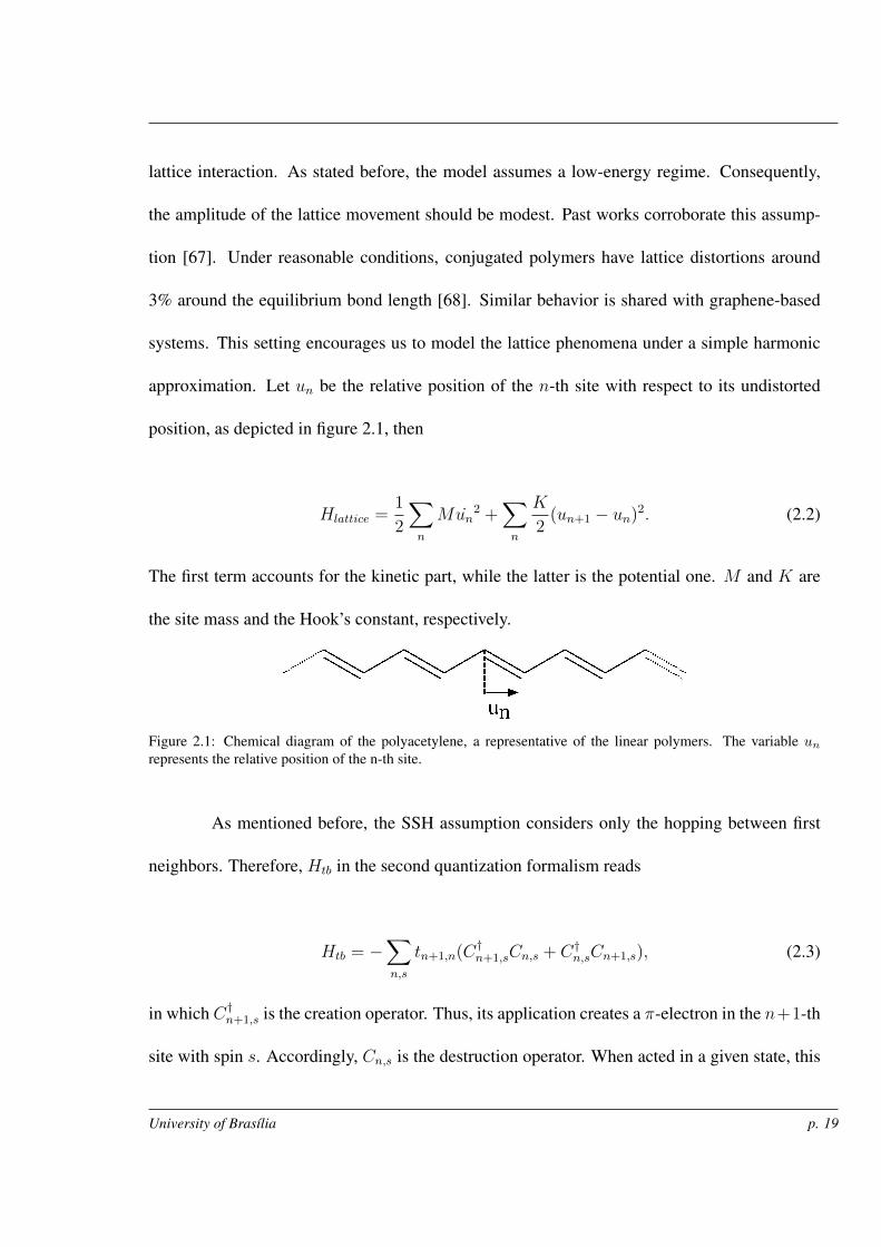
approximation. Let un be the relative position of the n-th site with respect to its undistorted
position, as depicted in figure 2.1, then
Hlattice =1
2
∑n
Mun2 +
∑n
K
2(un+1 − un)2. (2.2)
The first term accounts for the kinetic part, while the latter is the potential one. M and K are
the site mass and the Hook’s constant, respectively.
Figure 2.1: Chemical diagram of the polyacetylene, a representative of the linear polymers. The variable unrepresents the relative position of the n-th site.
As mentioned before, the SSH assumption considers only the hopping between first
neighbors. Therefore, Htb in the second quantization formalism reads
Htb = −∑n,s
tn+1,n(C†n+1,sCn,s + C†n,sCn+1,s), (2.3)
in which C†n+1,s is the creation operator. Thus, its application creates a π-electron in the n+1-th
site with spin s. Accordingly, Cn,s is the destruction operator. When acted in a given state, this
University of Brasília p. 19
operator annihilates a π-electron with spin s from the n-th site. tn+1,n is the so-called hopping
integral. It is associated with the amplitude probability of a π electron jump. Early devel-
opments treated tn+1,n as a constant regardless of the lattice spatial displacement. For some
systems, such approximation produces good results. However, as it is well known, transport in
graphene-based materials has a paramount influence of quasiparticles [69, 70, 71, 72]. These in-
dividuals rise from the interplay of the electronic and lattice phenomena. Therefore, refinement
of the hopping integral is a mandatory step to simulate more complex systems.
2.1.1 Electron-phonon Coupling Inclusion
There is not an analytical way to determine tn+1,n. However, it is possible to find an
approximated expression based on the type of system considered [73]. As stated before, the
distance between sites in conjugated polymers and graphene-based materials oscillate modestly
around the undistorted bond length value. Therefore, we are inclined to expand tn+1,n around
this reference distance [64]. In other words:
tn+1,n = t0 − α(un+1 − un). (2.4)
α is the electron-phonon coupling constant [67, 74]. As the name suggests, it dictates the lattice
influence over the electronic phenomena (and vice-versa). Each material presents a distinct
response. Therefore, α must be evaluated individually for every system. In this work, we
carried a tuning procedure based on the optical bandgap. The method is described in section
3.2.1.
University of Brasília p. 20
Here, we emphasize that the expected qualitative behavior holds. Given two adjacent
sites, tn+1,n must decrease as the inter-site distance grows. This is so because the more dis-
tant the sites are, the weaker the overlap between their pz orbitals will be. Thus, the hopping
becomes more difficult. In that sense, shrinking the distance must cause the inverse effect: an
increase in hopping rates. Furthermore, tn+1,n must return to a constant value (t0) in the absence
of distortions.
2.1.2 Solving the Electronic Hamiltonian
We initiate the solving procedure by the stationary case. For now, any site motion will
be discarded. Therefore,
un = 0 ∀n. (2.5)
This condition translates into
H = −∑n,s
tn+1,n(C†n+1,sCn,s + C†n,sCn+1,s) +
∑n
K
2(un+1 − un)2. (2.6)
Our objective is to diagonalize this operator. Because the Hamiltonian does not present any
term that couples electrons with a different spin, we can carry the diagonalization separately for
each spin s. Suppose that {ak,s} are the diagonalizing operators. Then,
H =∑k,s
Ek,sa†k,sak,s. (2.7)
University of Brasília p. 21
In order to explicitly find the diagonal form of Eq. 2.7 we must relate {Cn,s} and
{ak,s}. This is done by introducing a transformation such that
ak,s =∑n
bnksCn,s,
a†k,s =∑n
b∗nksC†n,s.
(2.8)
The coefficients must preserve probability. This forces us to also enforce unitary. Then,
for every eigenstate set with spin s,
b†b = 1, (2.9)
where each element in 1 holds, individually,
1n′n =∑k
(b)n′k(b†)kn =
∑k
(b)∗nk(b)n′k = δn′n,
1k′k =∑n
(b†)k′n(b)nk =∑n
(b)∗nk′(b)nk = δk′k.
(2.10)
Using these relations permit reverse Equation 2.8, leading to:
Cn,s =∑k
b∗nksak,s,
C†n,s =∑k
bnksa†k,s.
(2.11)
University of Brasília p. 22
Substitution in Eq. 2.6 gives
Hele = −∑n,s
∑k,k′
[tn+1,nbn+1ksb∗nk′s + t∗n+1,nbnksb
∗n+1k′s]a
†k,sak′,s
=∑k,s
Ek,sa†k,sak′,s =
∑k,k′,s
Ek,sδk,k′a†k,sak′,s
(2.12)
After reordering the summation indices and inserting 1 in the last equation, we get
−tn+1,nbn+1ks − t∗n,n−1bn−1ks = Eksbnks. (2.13)
The boundary terms require special care. Enforcing a periodic boundary relationship leads to
t0,n = tN,n,
tN+1,n = t1,n,
tn,0 = tn,N ,
tn,N+1 = tn,1.
(2.14)
Now, we are able to write the electronic Hamiltonian in matrix notation. Combining Eq. 2.13
University of Brasília p. 23
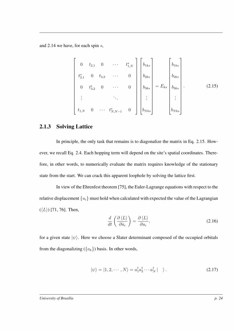
and 2.14 we have, for each spin s,
0 t2,1 0 · · · t∗1,N
t∗2,1 0 t3,2 · · · 0
0 t∗3,2 0 · · · 0
... . . .
t1,N 0 · · · t∗N,N−1 0
b1ks
b2ks
b3ks
...
bNks
= Eks
b1ks
b2ks
b3ks
...
bNks
. (2.15)
2.1.3 Solving Lattice
In principle, the only task that remains is to diagonalize the matrix in Eq. 2.15. How-
ever, we recall Eq. 2.4. Each hopping term will depend on the site’s spatial coordinates. There-
fore, in other words, to numerically evaluate the matrix requires knowledge of the stationary
state from the start. We can crack this apparent loophole by solving the lattice first.
In view of the Ehrenfest theorem [75], the Euler-Lagrange equations with respect to the
relative displacement {ui}must hold when calculated with expected the value of the Lagrangian
(〈L〉) [71, 76]. Then,
d
dt
(∂ 〈L〉∂ui
)=∂ 〈L〉∂ui
, (2.16)
for a given state |ψ〉. Here we choose a Slater determinant composed of the occupied orbitals
from the diagonalizing ({ak}) basis. In other words,
|ψ〉 = |1, 2, · · · , N〉 = a†1a†2 · · · a
†N | 〉 . (2.17)
University of Brasília p. 24
Let V and T be, respectively, the expected value of the potential and kinetic energy.
Recalling the stationary approximation, we have
〈L〉 = 〈T 〉 − 〈V 〉 = −〈V 〉 ,
〈L〉 = 〈ψ|
[∑n,s
tn+1,n(C†n+1Cn + C†nCn+1)−
∑n
K
2(ηn)
2
]|ψ〉 ,
〈L〉 =∑n,s
tn+1,n(〈C†n+1Cn〉+ 〈C†nCn+1〉)−∑n
K
2(ηn)
2.
(2.18)
Where, for convenience, we label ηi = ui+1 − ui. From Eq. 2.11 and 2.17
∑s
〈C†n+1,sCn,s〉 = 〈ψ|∑k,k′,s
bn+1ksb∗nk′sa
†k,sak′,s |ψ〉 ,
=∑k,k′,s
bn+1ksb∗nk′s 〈 | a1 · · · aN(a
†k,sak′,s)a
†1 · · · a
†N | 〉 ,
=∑′
k,s
bn+1ksb∗nks ≡ Bn+1n,
(2.19)
in which the prime sign indicates a summation over only the occupied orbitals. Then, rewriting
〈L〉 with this new notation gives
〈L〉 =∑n
tn+1n(Bn+1n +B∗n+1n)−∑n
K
2(un+1 − un)2,
=∑n
(t0 − αηn)(Bn+1n +B∗n+1n)−∑n
K
2(ηn)
2.
(2.20)
Taking the derivative of 〈L〉 with respect to an arbitrary ηn′ , and carrying out the sums leads to
∂ 〈L〉∂ηn′
= −α(Bn′+1n′ +B∗n′+1n′)−Kηn′ . (2.21)
University of Brasília p. 25
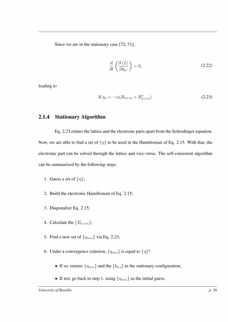
Since we are in the stationary case [72, 71],
d
dt
(∂ 〈L〉∂ηn′
)= 0, (2.22)
leading to
Kηn = −α(Bn+1n +B∗n+1n). (2.23)
2.1.4 Stationary Algorithm
Eq. 2.23 relates the lattice and the electronic parts apart from the Schrodinger equation.
Now, we are able to find a set of {η} to be used in the Hamiltonian of Eq. 2.15. With that, the
electronic part can be solved through the lattice and vice-versa. The self-consistent algorithm
can be summarized by the following steps:
1. Guess a set of {η};
2. Build the electronic Hamiltonian of Eq. 2.15;
3. Diagonalize Eq. 2.15;
4. Calculate the {Bn+1n};
5. Find a new set of {ηnew} via Eq. 2.23;
6. Under a convergence criterion, {ηnew} is equal to {η}?
• If so, returns {ηnew} and the {bk,s} as the stationary configuration;
• If not, go back to step 1. using {ηnew} as the initial guess.
University of Brasília p. 26
2.2 Generalization for 2-D Systems
Up to this point, all theoretical development described refers to one-dimensional poly-
mer chains. We now focus on adapting the preceding theory to two dimensional systems. In
order to do that, we must rewrite the Hamiltonian in Equation 2.1 considering the new lattice
profile. Unlike on the 1-D case, now each site may have up to three first neighbors. As a
consequence, the Hamiltonian turns into [71, 77, 78, 37, 79]
H = −∑
<i,j>,s
(t0 − αηi,j)(C†i,sCj,s + h.c.) +∑i
P 2i
2M+∑<i,j>
K
2η2i,j, (2.24)
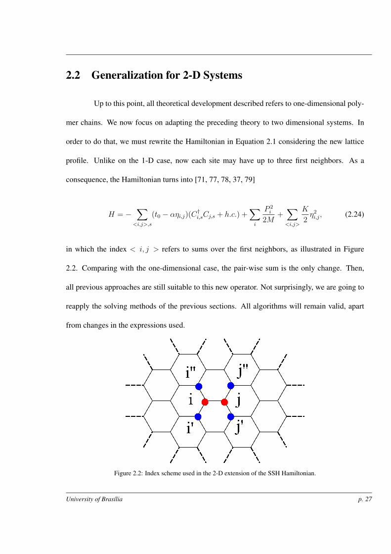
in which the index < i, j > refers to sums over the first neighbors, as illustrated in Figure
2.2. Comparing with the one-dimensional case, the pair-wise sum is the only change. Then,
all previous approaches are still suitable to this new operator. Not surprisingly, we are going to
reapply the solving methods of the previous sections. All algorithms will remain valid, apart
from changes in the expressions used.
Figure 2.2: Index scheme used in the 2-D extension of the SSH Hamiltonian.
University of Brasília p. 27
2.2.1 Stationary States
Recalling section 2.1.3, one must find the equations of motion of the generalized coor-
dinates to obtain stationary states. In a analogous procedure that ends in the Eq. 2.23, we reach
ηi,j = −α
K(Bi,j + h.c.), (2.25)
where Bi,j is defined according to Eq. 2.19. The solving procedure is analogous to the one
described for one-dimensional chains.
University of Brasília p. 28
CHAPTER 3
EDGE ENGINEERING IN COVE-TYPE GRAPHENE
NANORIBBONS
3.1 The Problem
Physicists and chemists are on the hunt to extend the properties of the cove-shaped
GNR [44] for future GNRs. This trend occurs because of the remarkable synthesis attributes
involved in this nanoribbon. Recent procedures enabled the production of CGNRs with different
widths via similar approaches. Now, as an additional step, one must find a way to explore one
of the most pertinent features of the GNRs: the striking dependence between the edge shape
and the physical properties [80]. Such a trait has a direct impact on future developing efforts. In
optoelectronics, the material’s usability depends on how easily its attributes can be mold, since
industrial demands can be highly particular, requiring fine adjustments. In that sense, finding a
precise way to tailor the physical properties of the CGNRs is a key task.
In most semiconductor-based devices, the energy bandgap is a decisive physical prop-
29
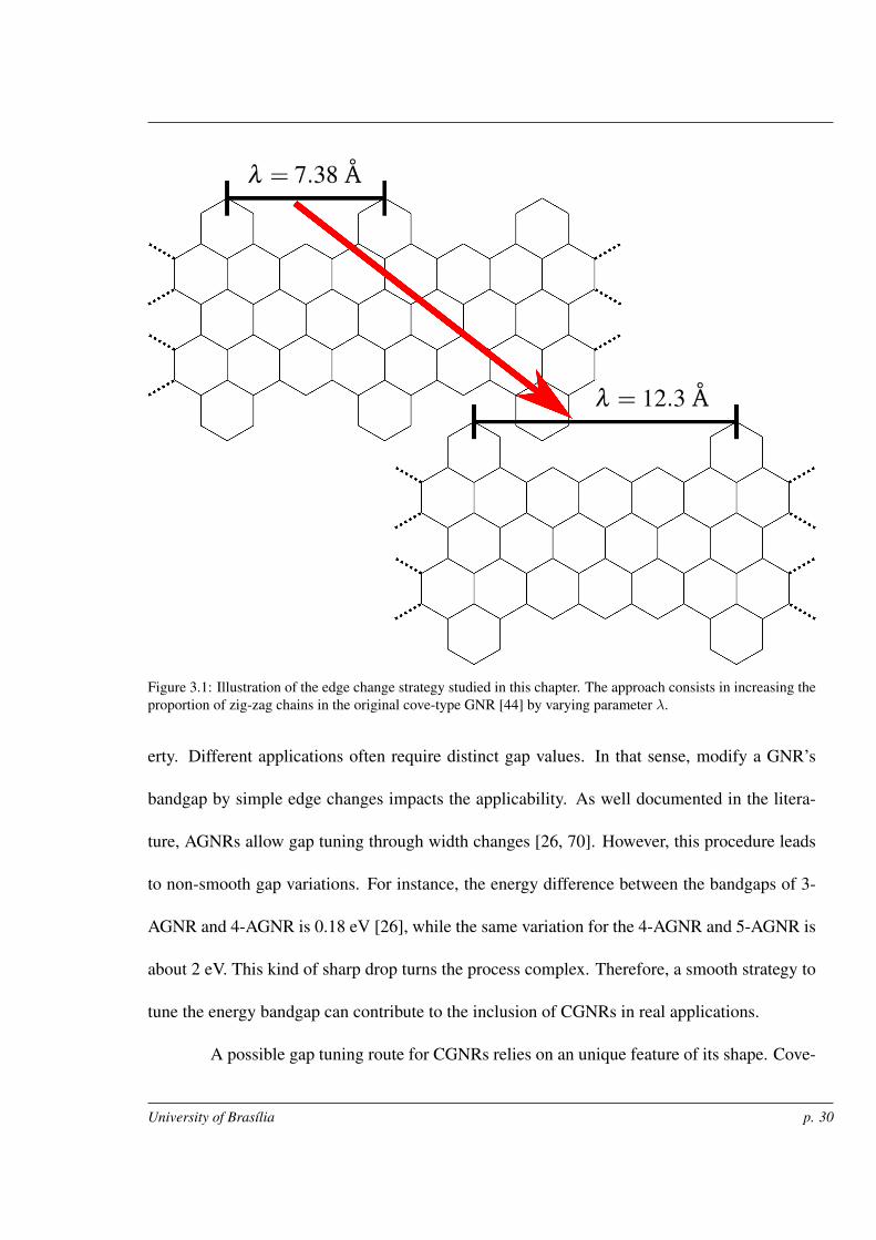
Figure 3.1: Illustration of the edge change strategy studied in this chapter. The approach consists in increasing theproportion of zig-zag chains in the original cove-type GNR [44] by varying parameter λ.
erty. Different applications often require distinct gap values. In that sense, modify a GNR’s
bandgap by simple edge changes impacts the applicability. As well documented in the litera-
ture, AGNRs allow gap tuning through width changes [26, 70]. However, this procedure leads
to non-smooth gap variations. For instance, the energy difference between the bandgaps of 3-
AGNR and 4-AGNR is 0.18 eV [26], while the same variation for the 4-AGNR and 5-AGNR is
about 2 eV. This kind of sharp drop turns the process complex. Therefore, a smooth strategy to
tune the energy bandgap can contribute to the inclusion of CGNRs in real applications.
A possible gap tuning route for CGNRs relies on an unique feature of its shape. Cove-
University of Brasília p. 30
shaped edges arise from the superposition of AGNR’s and ZGNR’s borders. As well known,
these two primordial GNRs may present opposite electronic properties [26, 28]. Because of
that, varying the proportion of each edge-shape should affect GNR’s gap. Figure 3.1 displays
this strategy. Unlike the width change approach, such a simple edge change does not alter the
nanoribbon’s quantum confinement degree. Therefore, it would likely drive minor disturbances
at the electronic properties. All the potential aside, this tuning strategy was not tested, until
now.
In this chapter, we present the results regarding the investigation of the aforementioned
edge change strategy in cove-type GNRs. Firstly, we estimate 4-CGNR’s α through a semi-
empirical approach. Then, the stationary algorithm is applied to CGNRs with different zig-
zag chain extensions. Each simulated specimen had its bandgap evaluated. In this study, we
considered four CGNRs types: 2-CGNR, 4-CGNR, 6-CGNR, and 8-CGNR. Results show a
smooth monotonic gap decay due to the increasing of zig-zag edges proportion. This declining
trend allows to smoothly reach band gaps between 0 eV to almost 3 eV. Also, we describe in
detail the effects of this approach on CGNR’s lattice. We observed that changing the proportion
of AGNR and ZGNR on the cove-edge modifies the conjugation rate. As a direct response, the
bond length distribution becomes significantly more disperse, translating into a morphological
spreading. The corresponding published paper of this work is located in the appendix section 4.
University of Brasília p. 31
3.2 Results
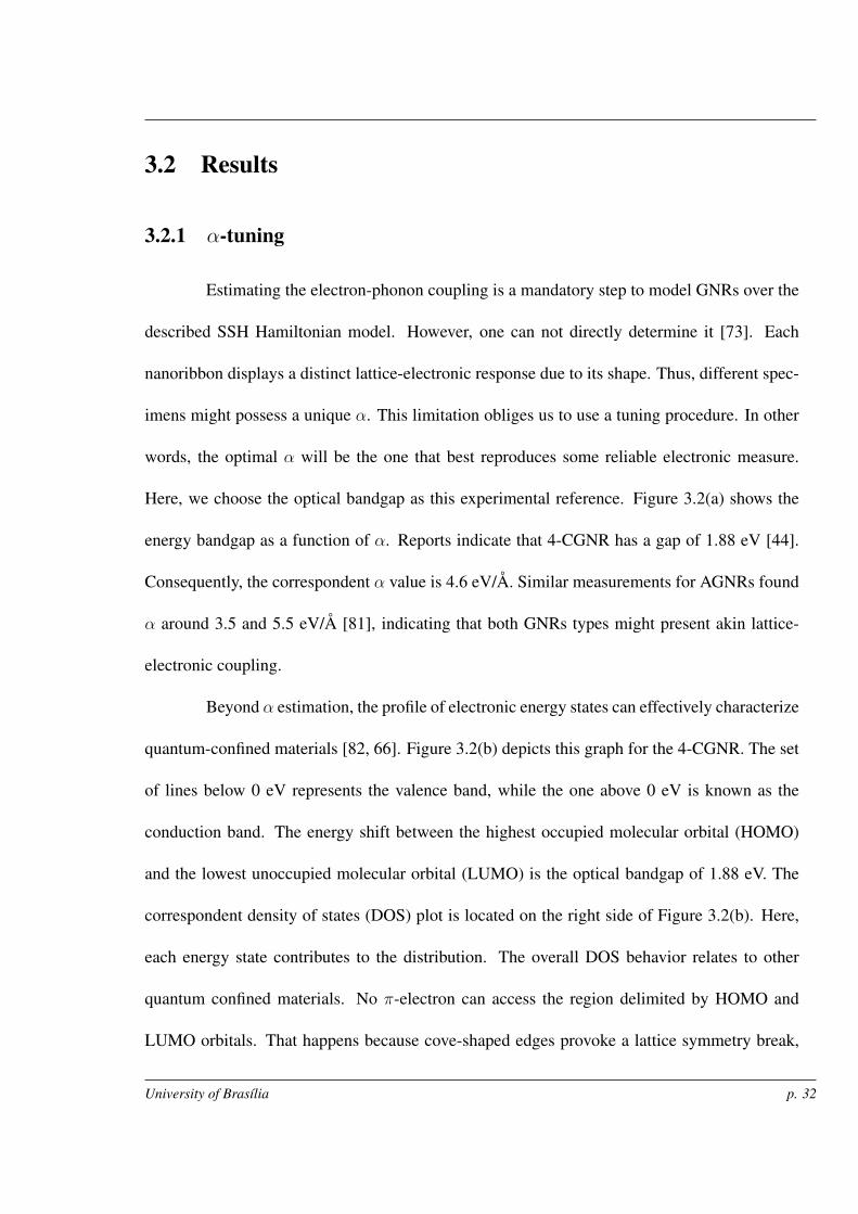
3.2.1 α-tuning
Estimating the electron-phonon coupling is a mandatory step to model GNRs over the
described SSH Hamiltonian model. However, one can not directly determine it [73]. Each
nanoribbon displays a distinct lattice-electronic response due to its shape. Thus, different spec-
imens might possess a unique α. This limitation obliges us to use a tuning procedure. In other
words, the optimal α will be the one that best reproduces some reliable electronic measure.
Here, we choose the optical bandgap as this experimental reference. Figure 3.2(a) shows the
energy bandgap as a function of α. Reports indicate that 4-CGNR has a gap of 1.88 eV [44].
Consequently, the correspondent α value is 4.6 eV/Å. Similar measurements for AGNRs found
α around 3.5 and 5.5 eV/Å [81], indicating that both GNRs types might present akin lattice-
electronic coupling.
Beyond α estimation, the profile of electronic energy states can effectively characterize
quantum-confined materials [82, 66]. Figure 3.2(b) depicts this graph for the 4-CGNR. The set
of lines below 0 eV represents the valence band, while the one above 0 eV is known as the
conduction band. The energy shift between the highest occupied molecular orbital (HOMO)
and the lowest unoccupied molecular orbital (LUMO) is the optical bandgap of 1.88 eV. The
correspondent density of states (DOS) plot is located on the right side of Figure 3.2(b). Here,
each energy state contributes to the distribution. The overall DOS behavior relates to other
quantum confined materials. No π-electron can access the region delimited by HOMO and
LUMO orbitals. That happens because cove-shaped edges provoke a lattice symmetry break,
University of Brasília p. 32
Figure 3.2: Electronic profile of the 4-CGNR. (a) shows the gap dependence over the electron-phonon couplingconstant. As α increases, the gap rises accordingly. This happens since strong couplings make any electronicphenomena more energetically expensive. Therefore, the energy cost to promote a π-electron from HOMO toLUMO also grows. (b) displays the electronic band structure with the adequate α. In the upper side, this is shownvia the density of the states. Below this graph, we display the respective energy levels.
University of Brasília p. 33
which makes a non-zero gap emerge. In addition, the number of states around HOMO and
LUMO increases. Similar behavior occurs in dimerized linear polymers and some AGNRs [63,
83, 74]. As for energies away from the forbidden region, the density grows notably higher, like
in AGNRs. That said, preliminary analysis infers that 4-CGNR has similar electronic behavior
to other GNRs.
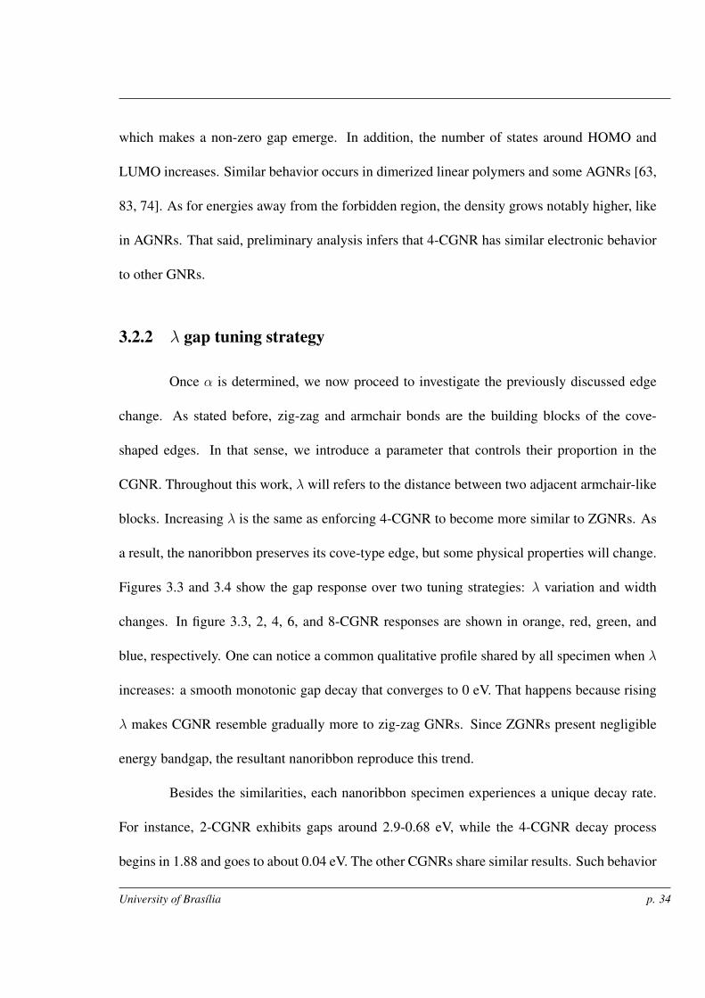
3.2.2 λ gap tuning strategy
Once α is determined, we now proceed to investigate the previously discussed edge
change. As stated before, zig-zag and armchair bonds are the building blocks of the cove-
shaped edges. In that sense, we introduce a parameter that controls their proportion in the
CGNR. Throughout this work, λ will refers to the distance between two adjacent armchair-like
blocks. Increasing λ is the same as enforcing 4-CGNR to become more similar to ZGNRs. As
a result, the nanoribbon preserves its cove-type edge, but some physical properties will change.
Figures 3.3 and 3.4 show the gap response over two tuning strategies: λ variation and width
changes. In figure 3.3, 2, 4, 6, and 8-CGNR responses are shown in orange, red, green, and
blue, respectively. One can notice a common qualitative profile shared by all specimen when λ
increases: a smooth monotonic gap decay that converges to 0 eV. That happens because rising
λ makes CGNR resemble gradually more to zig-zag GNRs. Since ZGNRs present negligible
energy bandgap, the resultant nanoribbon reproduce this trend.
Besides the similarities, each nanoribbon specimen experiences a unique decay rate.
For instance, 2-CGNR exhibits gaps around 2.9-0.68 eV, while the 4-CGNR decay process
begins in 1.88 and goes to about 0.04 eV. The other CGNRs share similar results. Such behavior
University of Brasília p. 34
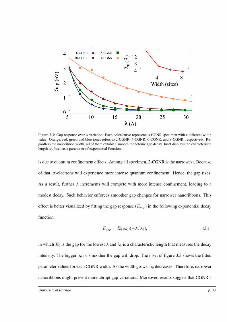
Figure 3.3: Gap response over λ variation. Each color/curve represents a CGNR specimen with a different widthvalue. Orange, red, green and blue tones refers to 2-CGNR, 4-CGNR, 6-CGNR, and 8-CGNR, respectively. Re-gardless the nanoribbon width, all of them exhibit a smooth monotonic gap decay. Inset displays the characteristiclength λ0 fitted as a parameter of exponential function.
is due to quantum confinement effects. Among all specimen, 2-CGNR is the narrowest. Because
of that, π-electrons will experience more intense quantum confinement. Hence, the gap rises.
As a result, further λ increments will compete with more intense confinement, leading to a
modest decay. Such behavior enforces smoother gap changes for narrower nanoribbons. This
effect is better visualized by fitting the gap response (Egap) in the following exponential decay
function:
Egap = E0 exp(−λ/λ0), (3.1)
in which E0 is the gap for the lowest λ and λ0 is a characteristic length that measures the decay
intensity. The bigger λ0 is, smoother the gap will drop. The inset of figure 3.3 shows the fitted
parameter values for each CGNR width. As the width grows, λ0 decreases. Therefore, narrower
nanoribbons might present more abrupt gap variations. Moreover, results suggest that CGNR’s
University of Brasília p. 35
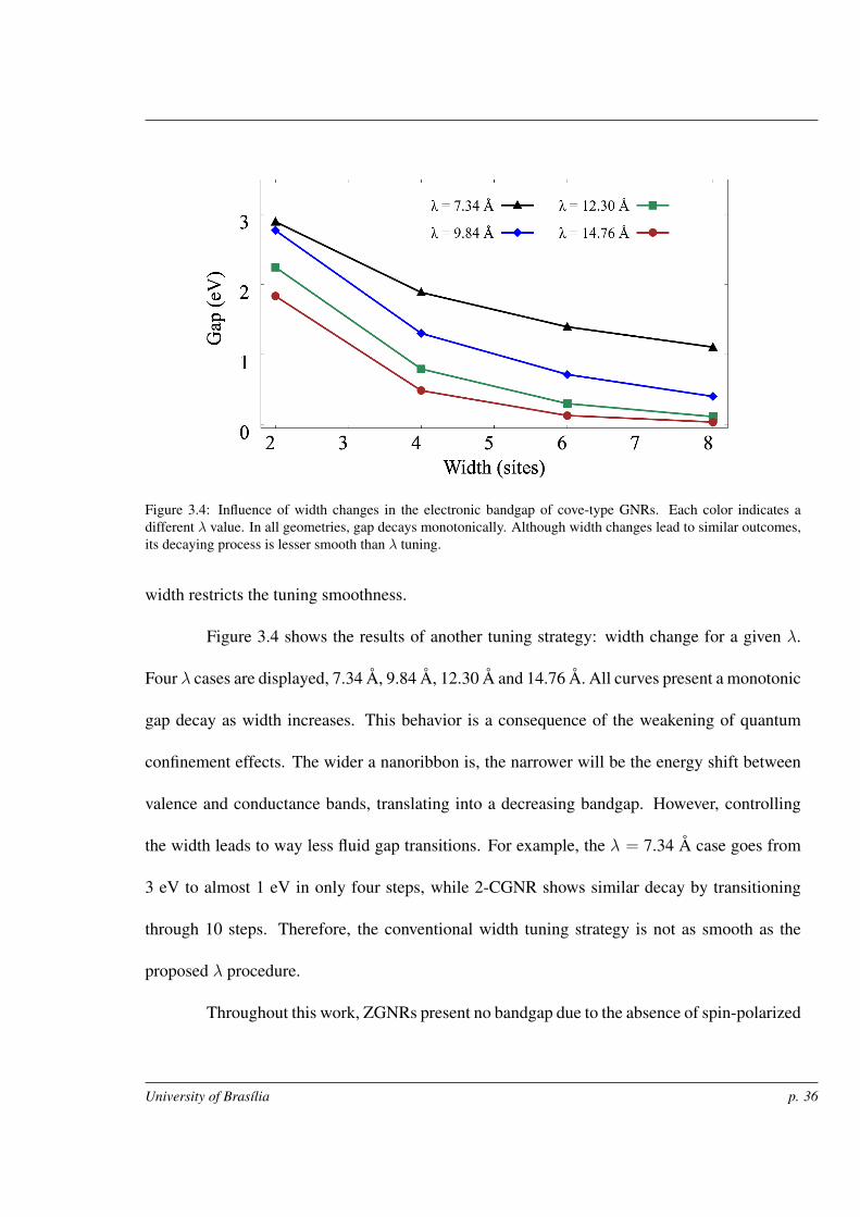
Figure 3.4: Influence of width changes in the electronic bandgap of cove-type GNRs. Each color indicates adifferent λ value. In all geometries, gap decays monotonically. Although width changes lead to similar outcomes,its decaying process is lesser smooth than λ tuning.
width restricts the tuning smoothness.
Figure 3.4 shows the results of another tuning strategy: width change for a given λ.
Four λ cases are displayed, 7.34 Å, 9.84 Å, 12.30 Å and 14.76 Å. All curves present a monotonic
gap decay as width increases. This behavior is a consequence of the weakening of quantum
confinement effects. The wider a nanoribbon is, the narrower will be the energy shift between
valence and conductance bands, translating into a decreasing bandgap. However, controlling
the width leads to way less fluid gap transitions. For example, the λ = 7.34 Å case goes from
3 eV to almost 1 eV in only four steps, while 2-CGNR shows similar decay by transitioning
through 10 steps. Therefore, the conventional width tuning strategy is not as smooth as the
proposed λ procedure.
Throughout this work, ZGNRs present no bandgap due to the absence of spin-polarized
University of Brasília p. 36
effects in our model [84, 85, 86]. The inclusion of such phenomena can induce gap opening
[84, 85, 87, 26], although we expect no substantial changes in the results. In that scenario, given
sufficient λ, each CGNR should converge to its correspondent ZGNR gap value. Regardless,
the profile of each nanoribbon will remain the same: a smooth monotonic gap decay.
The presented results show accordance with previous works. Until now, most of the
efforts aimed at the CGNR geometries with λ = 7.38Å [56, 35]. DFT-based investigations re-
ports 6-CGNR and 8-CGNR with a gap of 1.508 [88] and 1.24∓ 0.03 eV [44], respectively. On
the other hand, our method gives a gap of 1.394 eV for the former and 1.104 eV for the latter.
Such tight agreement is expected since similar approaches for other GNRs produce comparable
accuracy. For instance, simulations via local-density approximation (LDA) for the 5, 6, and
7-AGNRs estimate their gaps in 0.5, 1.1, and 1.65 eV, respectively [28, 26]. The same geome-
tries present gaps of 0.55, 1.75, and 1.78 eV when our methodology is applied. This steady
accordance trend, despite the nanoribbon type, reinforces the adequacy of our investigation
approach.
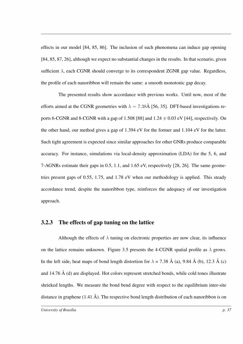
3.2.3 The effects of gap tuning on the lattice
Although the effects of λ tuning on electronic properties are now clear, its influence
on the lattice remains unknown. Figure 3.5 presents the 4-CGNR spatial profile as λ grows.
In the left side, heat maps of bond length distortion for λ = 7.38 Å (a), 9.84 Å (b), 12.3 Å (c)
and 14.76 Å (d) are displayed. Hot colors represent stretched bonds, while cold tones illustrate
shrieked lengths. We measure the bond bend degree with respect to the equilibrium inter-site
distance in graphene (1.41 Å). The respective bond length distribution of each nanoribbon is on
University of Brasília p. 37
Figure 3.5: Collection of bond length heatmaps and their respective histograms for 4-CGNR geometries with (a)λ = 7.38 Å, (b) 9.84 Å, (c) 12.3 Å, and (d) 14.76 Å. Hot and cold colors indicate stretching and compressionof bonds with respect to symmetric bond length, respectively. The histograms reveal that increases in λ induceschanges in conjugation degree and increases the morphological spreading
the right side. Nonetheless, the distortion’s magnitude is significantly smaller than the lattice
parameter, regardless of the λ value. In all cases, deformities not greater than 4 × 10⁻² Å
occur. This magnitude represents less than 3 % of the equilibrium separation distance, which
corroborates previous works [73, 89]. Moreover, these results reinforce the suitability of the
harmonic approximations.
The bond pattern of the original 4-CGNR (λ = 7.38 Å) consists of two arrangements:
a contraction-expansion alternation in the edges and a flower-like structure in the nanoribbon’s
core. In the edges, the proportion of contracted-type bonds outnumbers expanded-type ones.
University of Brasília p. 38
Conversely, the core contains a significant amount of undistorted and stretched bonds. In this
region, the aromatic rings surround every flower aggregate. The contribution of these two parts
results in the histogram located on the right side. One can notice four prominent peaks: a green
one located around the equilibrium bond length, a blue one centering in about 1.36 Å and two
red-like ones in 1.45 and 1.485 Å. The green peak is the greatest of all four and represents
almost 40 % of the lattice. The significant presence of undistorted bonds is due mostly to the
aromatic rings in the core. Contrastingly, the blue peak results solely from the contracted bonds
in the edges. As for the two hot-colored peaks, their origins differ. The more distorted one
emerges from the expanded-type edges bonds, while the other rises from the flower structure.
As λ grows, the distortion profile changes accordingly. Notable differences already
appear in the next configuration λ = 9.84 Å. The edge bonds still have an alternation pat-
tern. However, undistorted bonds also appear between two adjacent armchair-like structures.
Moreover, the flower-shaped pattern in the core disappears. Now, in this region, most of the
edges become slightly stretched or contracted. As a result, these bonds move away from the
aromatic length. Comparison with the corresponding histogram and the previous one reinforces
this observation. The four prominent peaks are converted into seven timid crests. This disper-
sion increase changes the conjugation degree. Therefore, results suggest that injecting zig-zag
chains in cove-type edges modifies lattice’s conjugation.
As the final discussion, we are going to address the effects of width changes in cove-
shaped GNRs. Figure 3.6 displays lattice distortion heatmaps for the 2-CGNR (a), 4-CGNR
(b), 6-CGNR (c), 8-CGNR (d) for λ = 7.38Å. In the same fashion of Figure 3.5, hot and cold
colors represent bond stretching and contraction, respectively. Moreover, each respective bond
University of Brasília p. 39
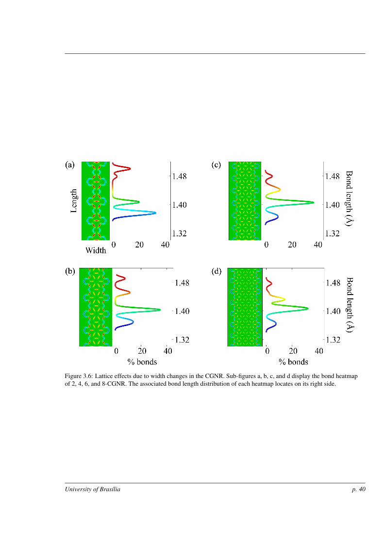
Figure 3.6: Lattice effects due to width changes in the CGNR. Sub-figures a, b, c, and d display the bond heatmapof 2, 4, 6, and 8-CGNR. The associated bond length distribution of each heatmap locates on its right side.
University of Brasília p. 40
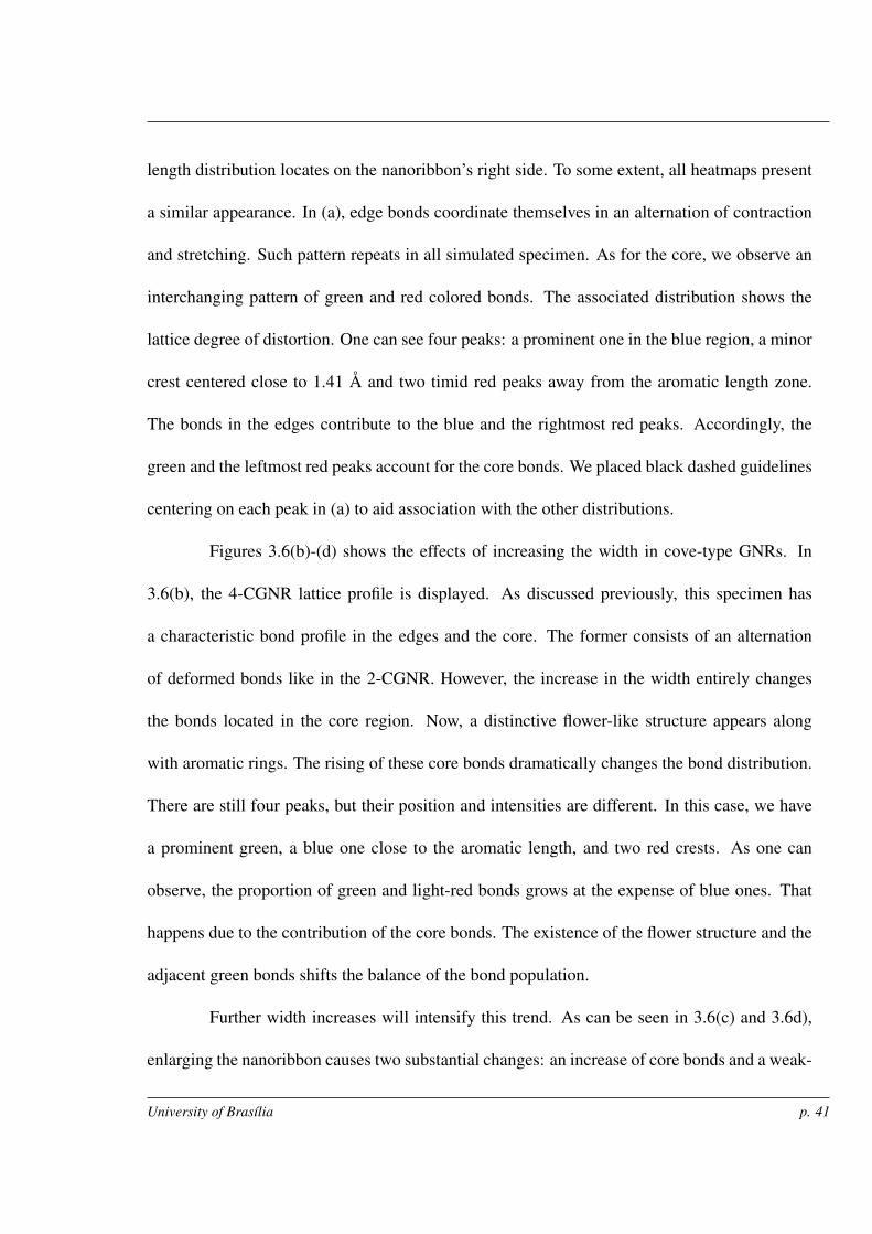
length distribution locates on the nanoribbon’s right side. To some extent, all heatmaps present
a similar appearance. In (a), edge bonds coordinate themselves in an alternation of contraction
and stretching. Such pattern repeats in all simulated specimen. As for the core, we observe an
interchanging pattern of green and red colored bonds. The associated distribution shows the
lattice degree of distortion. One can see four peaks: a prominent one in the blue region, a minor
crest centered close to 1.41 Å and two timid red peaks away from the aromatic length zone.
The bonds in the edges contribute to the blue and the rightmost red peaks. Accordingly, the
green and the leftmost red peaks account for the core bonds. We placed black dashed guidelines
centering on each peak in (a) to aid association with the other distributions.
Figures 3.6(b)-(d) shows the effects of increasing the width in cove-type GNRs. In
3.6(b), the 4-CGNR lattice profile is displayed. As discussed previously, this specimen has
a characteristic bond profile in the edges and the core. The former consists of an alternation
of deformed bonds like in the 2-CGNR. However, the increase in the width entirely changes
the bonds located in the core region. Now, a distinctive flower-like structure appears along
with aromatic rings. The rising of these core bonds dramatically changes the bond distribution.
There are still four peaks, but their position and intensities are different. In this case, we have
a prominent green, a blue one close to the aromatic length, and two red crests. As one can
observe, the proportion of green and light-red bonds grows at the expense of blue ones. That
happens due to the contribution of the core bonds. The existence of the flower structure and the
adjacent green bonds shifts the balance of the bond population.
Further width increases will intensify this trend. As can be seen in 3.6(c) and 3.6d),
enlarging the nanoribbon causes two substantial changes: an increase of core bonds and a weak-
University of Brasília p. 41
ening of the deformations in the flower structure. As a result, lightly stretched and undistorted
bonds contribute more to the distribution. Then, the bond distribution tends to concentrate
around the green region. This trend remains until the width becomes so large that the edge
bonds contribution turns negligible. At that stage, CGNRs exhibit a profile similar to pure zig-
zag GNRs. In addition, λ tuning seems to provoke a more deep morphological alteration in the
CGNRs.
3.3 Conclusion
In this work, we studied a potential edge change strategy that allows gap tuning in the
CGNR. The simulations were carried via the SSH model that accounts for the coupling between
lattice and electronic phenomena. Before digging into the problem, we first determined the
suitable electron-phonon coupling constant (α) for the CGNR to be 4.6 eV/Å. Comparison with
later reports confirms that CGNRs and AGNRs have a similar lattice-electronic response.
Next, we proceeded to carry the edge change modifications. Results show that increas-
ing the proportion of zig-zag edges in CGNR leads to a smooth gap drop. This conclusion
becomes even more evident when compared with width-change strategies. Therefore, due to
the unique shape of the CGNRs, they can endure a gap-tuning procedure more efficiently than
standard tuning approaches, showing smooth access to 40 gap values lying within the range of
0-3 eV. This feature contributes to the potential of such GNRs since it allows deeper tailoring
of the physical properties.
In addition, we also investigated the changes in the lattice as the tuning procedure
University of Brasília p. 42
unravels. We found that increasing the proportion of zig-zag edges leads to a systematic mor-
phological spreading in the bond length distribution. On the other hand, changes in the width
of the CGNR provoke distinct effects. As the width increases, the bond length distribution be-
comes more concentrated around the aromatic bond length. Thus, both strategies are physically
different.
The results obtained indicate that carrying such structural changes in the CGNR may
produce new materials with interesting electronic properties. As possible extension to this work,
we intend to explore the charge transport in the transformed morphology through dynamical
simulations of charged states. By doing that, we hope to characterize the charged quasiparticles
and their role in the transport, as well as the effects of structural changes in the phenomena.
University of Brasília p. 43
CHAPTER 4
PUBLISHED ARTICLE (RSC ADVANCES)
44
Smooth gap tuning strategy for cove-typegraphene nanoribbons
Tiago de Sousa Araujo Cassiano, a Fabio Ferreira Monteiro, a Leonardo Evaristode Sousa,b Geraldo Magela e Silvaa and Pedro Henrique de Oliveira Neto *a
Graphene is a carbon-based material with an extensive range of promising properties. Since it does not
present a bandgap, graphene is not suitable for optoelectronic applications. One possible way to open
a gap is achieved by reducing graphene to its nanoribbon (GNR) form. Recently, a GNR with well defined
cove-type periphery proper for large-scale production was synthesized showing an energy bandgap of
1.88 eV. In this work, we propose an edge termination strategy that allows for smoothly tuning the
energy bandgap of cove-type GNRs by systematically changing the periodicity with which armchair-like
and zigzag-like edges alternate. Using an extended two-dimensional Su–Schrieffer–Heeger tight-
binding model we compare the effects of this edge termination process on lattice deformation with
those arising from changes in nanoribbon width. Results show that modifications to the edges of cove-
type GNRs are able to smoothly reduce energy bandgaps at the expense of losses in conjugation and
increased morphological spreading. Energy band gap values starting from z3 eV to almost 0 eV were
obtained. The flexibility provided by this gap tuning procedure places the cove-type GNR as an
interesting candidate material for optoelectronic applications.
I. Introduction
Graphene is a two-dimensional system composed of honey-comb lattices of carbon atoms. It hosts a broad set of interestingphysical properties,1–5 resulting in the development of manygraphene based applications.6–9 A drawback prevents the use ofthese materials in optoelectronic devices: the absence of anenergy bandgap, which is the hallmark of semiconductormaterials. However, bandgap opening can be achieved bymeans of several approaches, such as a doping procedures,10–12
which consist in the addition of non-carbon atoms into thelattice. The injection of these atoms induces a symmetry breakin the system, leading to the appearance of a gap. Another wayto engineer a gap opening is through the reduction in one of thedimensions of the graphene sheet until it reaches atomic scales(several angstroms). These quasi one-dimensional graphenestrips are known as graphene nanorribons (GNRs).13,14 Due totheir limited size, quantum connement effects may arise,resulting in larger bandgaps. It is expected that GNRs will beginthe next generation of semiconductor applications.15–17
The properties of GNRs are directly related to their geome-tries, with edge structure and width extension playing a key roleon the electronic properties.18 Two edge shapes, known aszigzag (ZGNR) and armchair (AGNR) are specially relevant.
These AGNRs are usually classied by the number Na of atomsalong their width (Na-AGNR) and may be divided in threefamilies. These families are dened by Na ¼ 3p + 2, 3p + 1 and3p, where p is a positive integer. Importantly, ZGNRs andAGNRs from the 3p + 2 family do not present appreciablebandgaps, but, on the other hand, AGNRs from 3p and 3p + 1show semiconductor properties.13
Recently, a graphene nanoribbon with a new edge termina-tion was synthesized using a bottom-up liquid-phase proce-dure.19 The resultant GNR presented a cove-shaped edge (Fig. 1),which may be seen as a combination of the armchair and zigzagborders. Fig. 1(a) highlights examples of both border typesinside the CGNR, with a sample of an armchair and zigzagborder highlighted in red and blue, respectively. The synthesistechnique employed relies on the use of smaller compoundsthrough chemical reactions allowing an atomically precisedesign that mitigates structural defects and controls theproportion of each edge type. Known as cove-type GNR, orCGNR, this new nanoribbon architecture was reported asstructurally well-dened and unusually long (>200 nm).19
Gap tuning can be performed by modifying the AGNR'swidth.13,20,21 However, since each AGNR family presentsa particular gap dependence, this tuning procedure becomescomplex. For instance, the difference between the energybandgap of a 3-AGNR and 4-AGNR is about 0.18 eV.13 On theother hand, the gap variation between 4-AGNR and 5-AGNR isapproximately 2 eV. As such, a smooth gap tuning procedurebased on width changes in AGNRs is not possible.
aInstitute of Physics, University of Brasılia, Brazil. E-mail: [email protected] and Structural Chemistry Group, State University of Goias, Anapolis,
Goias, Brazil
Cite this: RSC Adv., 2020, 10, 26937
Received 2nd April 2020Accepted 29th June 2020
DOI: 10.1039/d0ra02997a
rsc.li/rsc-advances
This journal is © The Royal Society of Chemistry 2020 RSC Adv., 2020, 10, 26937–26943 | 26937
RSC Advances
PAPER
Ope
n A
cces
s A
rtic
le. P
ublis
hed
on 2
0 Ju
ly 2
020.
Dow
nloa
ded
on 1
1/24
/202
0 7:
27:4
6 PM
. T
his
artic
le is
lice
nsed
und
er a
Cre
ativ
e C
omm
ons
Attr
ibut
ion
3.0
Unp
orte
d L
icen
ce.
View Article OnlineView Journal | View Issue
Another possible strategy to tune energy gap relies on edgechanges. The literature provides several successful attemptsbased on morphological transformation.22–25 Nanopores placedon GNR's lattice are an example.26 The defect produced by thehole induces the formation of V-shaped edges. This new borderis a hybridization of armchair-like and zig-zag structures andcontrolling their relative amounts enables a smooth tuningprocedure to be undertaken. As mentioned before, CGNRs canhave its edge modied by a similar strategy. The question thenarises as to how such changes may affect the electronic prop-erties of these nanoribbons, as this could constitute a reliablemethod for gap tuning in GNRs.
To address the aforementioned issue, in this work, wesimulated several cove-edge terminations to investigate bothenergy bandgap and conjugation changes in CGNRs. Thenanoribbons were modelled using a two dimensional Su–Schrieffer–Heeger (SSH) model Hamiltonian. By means of a selfconsistent eld approach, we evaluated the bond lengthdistribution taking into consideration both electronic andphonon degrees of freedom. Our results show that changes ina single parameter that characterizes edge terminations leads toa monotonically decrease in the energy bandgap. By relating thebond length distribution pattern with the energy gap, thisphenomenon is shown to be a consequence of the superposi-tion of armchair and zigzag architectures. Gap values rangingfrom z3 eV to almost 0 eV were reached, showing that thismethod may be suitable for tailoring GNRs for very specicapplications.
II. Methods
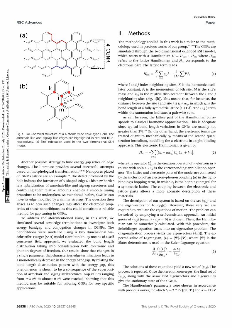
The methodology applied in this work is similar to the meth-odology used in previous works of our group.27–30 The GNRs aresimulated through the two dimensional extended SSH model,which starts with a Hamiltonian H ¼ Hlatt + Htb, where Hlatt
refers to the lattice Hamiltonian and Htb corresponds to theelectronic part. The lattice term reads
Hlatt ¼ K
2
Xhi;ji
hi;j2 þ 1
2M
Xi
Pi2; (1)
where i and j index neighboring sites, K is the harmonic oscil-lator constant, Pi is the momentum of i-th site, M is the site'smass and hi,j is the relative displacement between the i and jneighboring sites (Fig. 1(b)). This means that, for instance, thedistance between the site i and site j is l0 + hi,j, in which l0 is thebond length of a fully symmetric lattice (1.41 A). The h i,j i termwithin the summation indicates a pair-wise sum.
As can be seen, the lattice part of the Hamiltonian corre-sponds to classical harmonic approximation. This is adequatesince typical bond length variations in GNRs are usually notgreater than 2%.29 On the other hand, the electronic terms aretreated quantum mechanically by means of the second quan-tization formalism, modelling the p-electrons in a tight-bindingapproach. This electronic Hamiltonian is given by
Htb ¼ �Xhi;j;si
��t0 � ahi;j
�C
†i;sCj;s þ h:c
�; (2)
where the operator C†i;s is the creation operator of p-electron in i-
th site with spin s. Ci,s is the corresponding annihilation oper-ator. The lattice and electronic parts of the model are connectedby the inclusion of an electron–phonon coupling (a) in the tight-binding's hopping term, in which t0 is the hopping integral fora symmetric lattice. The coupling between the electronic andlattice parts allows a more accurate description of thesematerials.
The description of our system is based on the set {hi,j} andthe eigenvectors of H, {jk(i)}. However, these very set arerequired to evaluate the equations of motion. The problem canbe solved by employing a self-consistent approach. An initialguess of {hi,j} (usually {hi,j} ¼ 0) is chosen. Then, the Hamilto-nian can be numerically calculated. With this procedure, theSchrodinger equation turns into an eigenvalue problem. Thediagonalization process yields the eigenvectors {jk(i)}. The ex-pected value of Lagrangian, hLi ¼ hJ|L|Ji, where |Ji is theSlater determinant is used in the Euler–Lagrange equation,
d
dt
�vhLivh
�
i;j
�¼ vhLi
vhi;j
: (3)
The solutions of these equations yield a new set of {hi,j}. Theprocess is repeated. Once the iteration converges, the nal set of{hi,j}, along with the associated eigenvectors and eigenvaluesgive the stationary state of the CGNR.
The Hamiltonian's parameters were chosen in accordancewith previous works, for which t0¼ 2.7 eV (ref. 31) and K¼ 21 eV
Fig. 1 (a) Chemical structure of a 4 atoms wide cove-type GNR. Thearmchair-like and zigzag-like edges are highlighted in red and blue,respectively. (b) Site indexation used in the two-dimensional SSHmodel.
26938 | RSC Adv., 2020, 10, 26937–26943 This journal is © The Royal Society of Chemistry 2020
RSC Advances Paper
Ope
n A
cces
s A
rtic
le. P
ublis
hed
on 2
0 Ju
ly 2
020.
Dow
nloa
ded
on 1
1/24
/202
0 7:
27:4
6 PM
. T
his
artic
le is
lice
nsed
und
er a
Cre
ativ
e C
omm
ons
Attr
ibut
ion
3.0
Unp
orte
d L
icen
ce.
View Article Online
A�2.32 As for the electron–phonon constant, its evaluation isdone through a semi-empirical procedure which will bedescribed in the results session. Finally, as the number ofcarbon atoms on the width classies armchair graphenenanoribbons, the same criterion will be applied throughout thiswork. For instance, the CGNR from Fig. 1(a) exhibits fourcarbons along the width axis, therefore, we refer to it as 4-CGNR.For the length direction, periodic boundary conditions areemployed.
III. Results
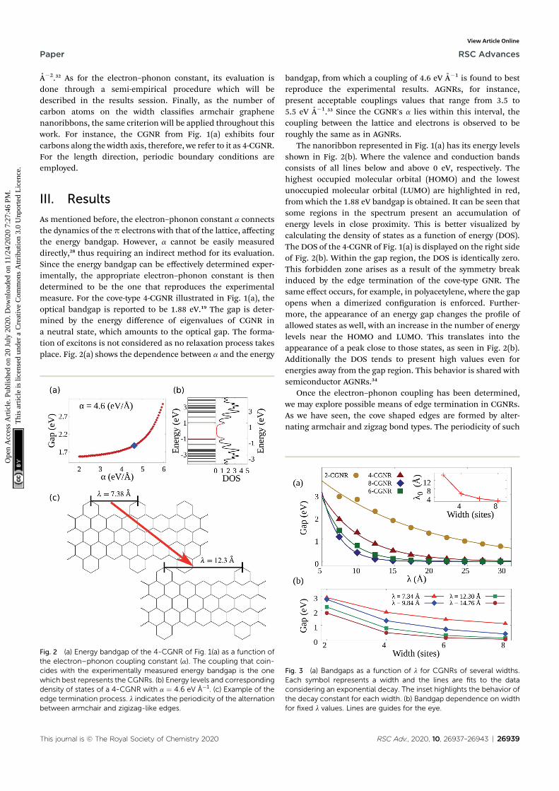
As mentioned before, the electron–phonon constant a connectsthe dynamics of the p electrons with that of the lattice, affectingthe energy bandgap. However, a cannot be easily measureddirectly,28 thus requiring an indirect method for its evaluation.Since the energy bandgap can be effectively determined exper-imentally, the appropriate electron–phonon constant is thendetermined to be the one that reproduces the experimentalmeasure. For the cove-type 4-CGNR illustrated in Fig. 1(a), theoptical bandgap is reported to be 1.88 eV.19 The gap is deter-mined by the energy difference of eigenvalues of CGNR ina neutral state, which amounts to the optical gap. The forma-tion of excitons is not considered as no relaxation process takesplace. Fig. 2(a) shows the dependence between a and the energy
bandgap, from which a coupling of 4.6 eV A�1 is found to bestreproduce the experimental results. AGNRs, for instance,present acceptable couplings values that range from 3.5 to5.5 eV A�1.33 Since the CGNR's a lies within this interval, thecoupling between the lattice and electrons is observed to beroughly the same as in AGNRs.
The nanoribbon represented in Fig. 1(a) has its energy levelsshown in Fig. 2(b). Where the valence and conduction bandsconsists of all lines below and above 0 eV, respectively. Thehighest occupied molecular orbital (HOMO) and the lowestunoccupied molecular orbital (LUMO) are highlighted in red,from which the 1.88 eV bandgap is obtained. It can be seen thatsome regions in the spectrum present an accumulation ofenergy levels in close proximity. This is better visualized bycalculating the density of states as a function of energy (DOS).The DOS of the 4-CGNR of Fig. 1(a) is displayed on the right sideof Fig. 2(b). Within the gap region, the DOS is identically zero.This forbidden zone arises as a result of the symmetry breakinduced by the edge termination of the cove-type GNR. Thesame effect occurs, for example, in polyacetylene, where the gapopens when a dimerized conguration is enforced. Further-more, the appearance of an energy gap changes the prole ofallowed states as well, with an increase in the number of energylevels near the HOMO and LUMO. This translates into theappearance of a peak close to those states, as seen in Fig. 2(b).Additionally the DOS tends to present high values even forenergies away from the gap region. This behavior is shared withsemiconductor AGNRs.34
Once the electron–phonon coupling has been determined,we may explore possible means of edge termination in CGNRs.As we have seen, the cove shaped edges are formed by alter-nating armchair and zigzag bond types. The periodicity of such
Fig. 2 (a) Energy bandgap of the 4-CGNR of Fig. 1(a) as a function ofthe electron–phonon coupling constant (a). The coupling that coin-cides with the experimentally measured energy bandgap is the onewhich best represents the CGNRs. (b) Energy levels and correspondingdensity of states of a 4-CGNR with a ¼ 4.6 eV A�1. (c) Example of theedge termination process. l indicates the periodicity of the alternationbetween armchair and zigizag-like edges.
Fig. 3 (a) Bandgaps as a function of l for CGNRs of several widths.Each symbol represents a width and the lines are fits to the dataconsidering an exponential decay. The inset highlights the behavior ofthe decay constant for each width. (b) Bandgap dependence on widthfor fixed l values. Lines are guides for the eye.
This journal is © The Royal Society of Chemistry 2020 RSC Adv., 2020, 10, 26937–26943 | 26939
Paper RSC Advances
Ope
n A
cces
s A
rtic
le. P
ublis
hed
on 2
0 Ju
ly 2
020.
Dow
nloa
ded
on 1
1/24
/202
0 7:
27:4
6 PM
. T
his
artic
le is
lice
nsed
und
er a
Cre
ativ
e C
omm
ons
Attr
ibut
ion
3.0
Unp
orte
d L
icen
ce.
View Article Online
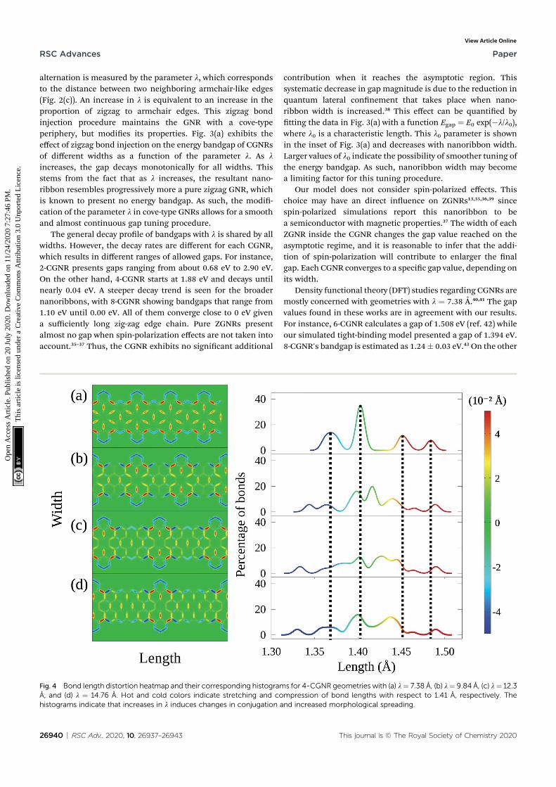
alternation is measured by the parameter l, which correspondsto the distance between two neighboring armchair-like edges(Fig. 2(c)). An increase in l is equivalent to an increase in theproportion of zigzag to armchair edges. This zigzag bondinjection procedure maintains the GNR with a cove-typeperiphery, but modies its properties. Fig. 3(a) exhibits theeffect of zigzag bond injection on the energy bandgap of CGNRsof different widths as a function of the parameter l. As l
increases, the gap decays monotonically for all widths. Thisstems from the fact that as l increases, the resultant nano-ribbon resembles progressively more a pure zigzag GNR, whichis known to present no energy bandgap. As such, the modi-cation of the parameter l in cove-type GNRs allows for a smoothand almost continuous gap tuning procedure.
The general decay prole of bandgaps with l is shared by allwidths. However, the decay rates are different for each CGNR,which results in different ranges of allowed gaps. For instance,2-CGNR presents gaps ranging from about 0.68 eV to 2.90 eV.On the other hand, 4-CGNR starts at 1.88 eV and decays untilnearly 0.04 eV. A steeper decay trend is seen for the broadernanoribbons, with 8-CGNR showing bandgaps that range from1.10 eV until 0.00 eV. All of them converge close to 0 eV givena sufficiently long zig-zag edge chain. Pure ZGNRs presentalmost no gap when spin-polarization effects are not taken intoaccount.35–37 Thus, the CGNR exhibits no signicant additional
contribution when it reaches the asymptotic region. Thissystematic decrease in gap magnitude is due to the reduction inquantum lateral connement that takes place when nano-ribbon width is increased.38 This effect can be quantied bytting the data in Fig. 3(a) with a function Egap ¼ E0 exp(�l/l0),where l0 is a characteristic length. This l0 parameter is shownin the inset of Fig. 3(a) and decreases with nanoribbon width.Larger values of l0 indicate the possibility of smoother tuning ofthe energy bandgap. As such, nanoribbon width may becomea limiting factor for this tuning procedure.
Our model does not consider spin-polarized effects. Thischoice may have an direct inuence on ZGNRs13,35,36,39 sincespin-polarized simulations report this nanoribbon to bea semiconductor with magnetic properties.37 The width of eachZGNR inside the CGNR changes the gap value reached on theasymptotic regime, and it is reasonable to infer that the addi-tion of spin-polarization will contribute to enlarger the nalgap. Each CGNR converges to a specic gap value, depending onits width.
Density functional theory (DFT) studies regarding CGNRs aremostly concerned with geometries with l ¼ 7.38 A.40,41 The gapvalues found in these works are in agreement with our results.For instance, 6-CGNR calculates a gap of 1.508 eV (ref. 42) whileour simulated tight-binding model presented a gap of 1.394 eV.8-CGNR's bandgap is estimated as 1.24� 0.03 eV.43 On the other
Fig. 4 Bond length distortion heatmap and their corresponding histograms for 4-CGNR geometries with (a) l¼ 7.38 A, (b) l¼ 9.84 A, (c) l¼ 12.3A, and (d) l ¼ 14.76 A. Hot and cold colors indicate stretching and compression of bond lengths with respect to 1.41 A, respectively. Thehistograms indicate that increases in l induces changes in conjugation and increased morphological spreading.
26940 | RSC Adv., 2020, 10, 26937–26943 This journal is © The Royal Society of Chemistry 2020
RSC Advances Paper
Ope
n A
cces
s A
rtic
le. P
ublis
hed
on 2
0 Ju
ly 2
020.
Dow
nloa
ded
on 1
1/24
/202
0 7:
27:4
6 PM
. T
his
artic
le is
lice
nsed
und
er a
Cre
ativ
e C
omm
ons
Attr
ibut
ion
3.0
Unp
orte
d L
icen
ce.
View Article Online
hand, our calculations showed a gap of 1.104 eV. This accor-dance trend is shared with AGNR as well. For instance, LDAcalculations show 5, 6, and 7-AGNR with, respectively, z0.5,1.1, 1.65 eV.13,21 Our method evaluates the gap from the samegeometries, respectively, 0.55, 1.75, 1.78 eV. This visible agree-ment shows the suitability of the presented methodology.
The effects of varying nanoribbon width for a given l can beseen in Fig. 3(b). In wider nanoribbons, quantum connementeffects become weaker, reducing energy bandgaps accordingly.A similar dependence between gap and width size has beenobserved in AGNRs as well.13 However, it is also clear thatchanges in width do not produce bandgap reductions assmooth as those observed by increasing l. This is so because, bypreserving the edge structure, changes in width do not translateinto a transformation from armchair-like to zigzag-like nano-ribbons, which possess completely different bandgap proper-ties. As such, controlling nanoribbon width does not constitutea tuning procedure as effective as controlling l.
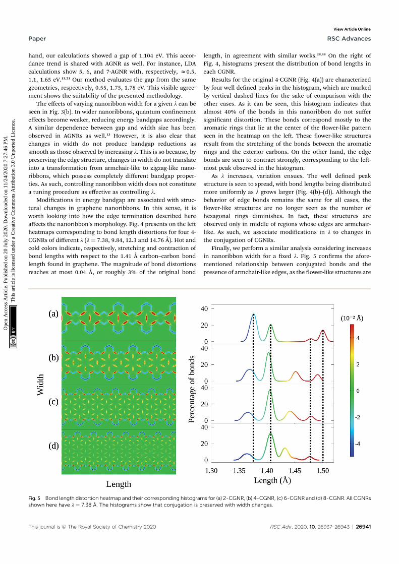
Modications in energy bandgap are associated with struc-tural changes in graphene nanoribbons. In this sense, it isworth looking into how the edge termination described hereaffects the nanoribbon's morphology. Fig. 4 presents on the leheatmaps corresponding to bond length distortions for four 4-CGNRs of different l (l ¼ 7.38, 9.84, 12.3 and 14.76 A). Hot andcold colors indicate, respectively, stretching and contraction ofbond lengths with respect to the 1.41 A carbon–carbon bondlength found in graphene. The magnitude of bond distortionsreaches at most 0.04 A, or roughly 3% of the original bond
length, in agreement with similar works.28,44 On the right ofFig. 4, histograms present the distribution of bond lengths ineach CGNR.
Results for the original 4-CGNR (Fig. 4(a)) are characterizedby four well dened peaks in the histogram, which are markedby vertical dashed lines for the sake of comparison with theother cases. As it can be seen, this histogram indicates thatalmost 40% of the bonds in this nanoribbon do not suffersignicant distortion. These bonds correspond mostly to thearomatic rings that lie at the center of the ower-like patternseen in the heatmap on the le. These ower-like structuresresult from the stretching of the bonds between the aromaticrings and the exterior carbons. On the other hand, the edgebonds are seen to contract strongly, corresponding to the le-most peak observed in the histogram.
As l increases, variation ensues. The well dened peakstructure is seen to spread, with bond lengths being distributedmore uniformly as l grows larger (Fig. 4(b)–(d)). Although thebehavior of edge bonds remains the same for all cases, theower-like structures are no longer seen as the number ofhexagonal rings diminishes. In fact, these structures areobserved only in middle of regions whose edges are armchair-like. As such, we associate modications in l to changes inthe conjugation of CGNRs.
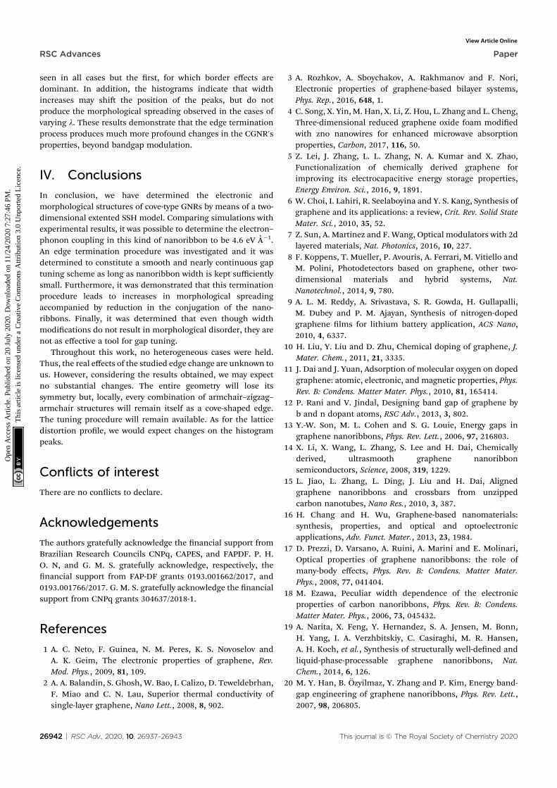
Finally, we perform a similar analysis considering increasesin nanoribbon width for a xed l. Fig. 5 conrms the afore-mentioned relationship between conjugated bonds and thepresence of armchair-like edges, as the ower-like structures are
Fig. 5 Bond length distortion heatmap and their corresponding histograms for (a) 2-CGNR, (b) 4-CGNR, (c) 6-CGNR and (d) 8-CGNR. All CGNRsshown here have l ¼ 7.38 A. The histograms show that conjugation is preserved with width changes.
This journal is © The Royal Society of Chemistry 2020 RSC Adv., 2020, 10, 26937–26943 | 26941
Paper RSC Advances
Ope
n A
cces
s A
rtic
le. P
ublis
hed
on 2
0 Ju
ly 2
020.
Dow
nloa
ded
on 1
1/24
/202
0 7:
27:4
6 PM
. T
his
artic
le is
lice
nsed
und
er a
Cre
ativ
e C
omm
ons
Attr
ibut
ion
3.0
Unp
orte
d L
icen
ce.
View Article Online
seen in all cases but the rst, for which border effects aredominant. In addition, the histograms indicate that widthincreases may shi the position of the peaks, but do notproduce the morphological spreading observed in the cases ofvarying l. These results demonstrate that the edge terminationprocess produces much more profound changes in the CGNR'sproperties, beyond bandgap modulation.
IV. Conclusions
In conclusion, we have determined the electronic andmorphological structures of cove-type GNRs by means of a two-dimensional extented SSH model. Comparing simulations withexperimental results, it was possible to determine the electron–phonon coupling in this kind of nanoribbon to be 4.6 eV A�1.An edge termination procedure was investigated and it wasdetermined to constitute a smooth and nearly continuous gaptuning scheme as long as nanoribbon width is kept sufficientlysmall. Furthermore, it was demonstrated that this terminationprocedure leads to increases in morphological spreadingaccompanied by reduction in the conjugation of the nano-ribbons. Finally, it was determined that even though widthmodications do not result in morphological disorder, they arenot as effective a tool for gap tuning.
Throughout this work, no heterogeneous cases were held.Thus, the real effects of the studied edge change are unknown tous. However, considering the results obtained, we may expectno substantial changes. The entire geometry will lose itssymmetry but, locally, every combination of armchair–zigzag–armchair structures will remain itself as a cove-shaped edge.The tuning procedure will remain available. As for the latticedistortion prole, we would expect changes on the histogrampeaks.
Conflicts of interest
There are no conicts to declare.
Acknowledgements
The authors gratefully acknowledge the nancial support fromBrazilian Research Councils CNPq, CAPES, and FAPDF. P. H.O. N, and G. M. S. gratefully acknowledge, respectively, thenancial support from FAP-DF grants 0193.001662/2017, and0193.001766/2017. G. M. S. gratefully acknowledge the nancialsupport from CNPq grants 304637/2018-1.
References
1 A. C. Neto, F. Guinea, N. M. Peres, K. S. Novoselov andA. K. Geim, The electronic properties of graphene, Rev.Mod. Phys., 2009, 81, 109.
2 A. A. Balandin, S. Ghosh, W. Bao, I. Calizo, D. Teweldebrhan,F. Miao and C. N. Lau, Superior thermal conductivity ofsingle-layer graphene, Nano Lett., 2008, 8, 902.
3 A. Rozhkov, A. Sboychakov, A. Rakhmanov and F. Nori,Electronic properties of graphene-based bilayer systems,Phys. Rep., 2016, 648, 1.
4 C. Song, X. Yin, M. Han, X. Li, Z. Hou, L. Zhang and L. Cheng,Three-dimensional reduced graphene oxide foam modiedwith zno nanowires for enhanced microwave absorptionproperties, Carbon, 2017, 116, 50.
5 Z. Lei, J. Zhang, L. L. Zhang, N. A. Kumar and X. Zhao,Functionalization of chemically derived graphene forimproving its electrocapacitive energy storage properties,Energy Environ. Sci., 2016, 9, 1891.
6 W. Choi, I. Lahiri, R. Seelaboyina and Y. S. Kang, Synthesis ofgraphene and its applications: a review, Crit. Rev. Solid StateMater. Sci., 2010, 35, 52.
7 Z. Sun, A. Martinez and F. Wang, Optical modulators with 2dlayered materials, Nat. Photonics, 2016, 10, 227.
8 F. Koppens, T. Mueller, P. Avouris, A. Ferrari, M. Vitiello andM. Polini, Photodetectors based on graphene, other two-dimensional materials and hybrid systems, Nat.Nanotechnol., 2014, 9, 780.
9 A. L. M. Reddy, A. Srivastava, S. R. Gowda, H. Gullapalli,M. Dubey and P. M. Ajayan, Synthesis of nitrogen-dopedgraphene lms for lithium battery application, ACS Nano,2010, 4, 6337.
10 H. Liu, Y. Liu and D. Zhu, Chemical doping of graphene, J.Mater. Chem., 2011, 21, 3335.
11 J. Dai and J. Yuan, Adsorption of molecular oxygen on dopedgraphene: atomic, electronic, and magnetic properties, Phys.Rev. B: Condens. Matter Mater. Phys., 2010, 81, 165414.
12 P. Rani and V. Jindal, Designing band gap of graphene byb and n dopant atoms, RSC Adv., 2013, 3, 802.
13 Y.-W. Son, M. L. Cohen and S. G. Louie, Energy gaps ingraphene nanoribbons, Phys. Rev. Lett., 2006, 97, 216803.
14 X. Li, X. Wang, L. Zhang, S. Lee and H. Dai, Chemicallyderived, ultrasmooth graphene nanoribbonsemiconductors, Science, 2008, 319, 1229.
15 L. Jiao, L. Zhang, L. Ding, J. Liu and H. Dai, Alignedgraphene nanoribbons and crossbars from unzippedcarbon nanotubes, Nano Res., 2010, 3, 387.
16 H. Chang and H. Wu, Graphene-based nanomaterials:synthesis, properties, and optical and optoelectronicapplications, Adv. Funct. Mater., 2013, 23, 1984.
17 D. Prezzi, D. Varsano, A. Ruini, A. Marini and E. Molinari,Optical properties of graphene nanoribbons: the role ofmany-body effects, Phys. Rev. B: Condens. Matter Mater.Phys., 2008, 77, 041404.
18 M. Ezawa, Peculiar width dependence of the electronicproperties of carbon nanoribbons, Phys. Rev. B: Condens.Matter Mater. Phys., 2006, 73, 045432.
19 A. Narita, X. Feng, Y. Hernandez, S. A. Jensen, M. Bonn,H. Yang, I. A. Verzhbitskiy, C. Casiraghi, M. R. Hansen,A. H. Koch, et al., Synthesis of structurally well-dened andliquid-phase-processable graphene nanoribbons, Nat.Chem., 2014, 6, 126.
20 M. Y. Han, B. Ozyilmaz, Y. Zhang and P. Kim, Energy band-gap engineering of graphene nanoribbons, Phys. Rev. Lett.,2007, 98, 206805.
26942 | RSC Adv., 2020, 10, 26937–26943 This journal is © The Royal Society of Chemistry 2020
RSC Advances Paper
Ope
n A
cces
s A
rtic
le. P
ublis
hed
on 2
0 Ju
ly 2
020.
Dow
nloa
ded
on 1
1/24
/202
0 7:
27:4
6 PM
. T
his
artic
le is
lice
nsed
und
er a
Cre
ativ
e C
omm
ons
Attr
ibut
ion
3.0
Unp
orte
d L
icen
ce.
View Article Online
21 L. Yang, C.-H. Park, Y.-W. Son, M. L. Cohen and S. G. Louie,Quasiparticle energies and band gaps in graphenenanoribbons, Phys. Rev. Lett., 2007, 99, 186801.
22 P. Wagner, C. P. Ewels, J.-J. Adjizian, L. Magaud, P. Pochet,S. Roche, A. Lopez-Bezanilla, V. V. Ivanovskaya, A. Yaya,M. Rayson, et al., Band gap engineering via edge-functionalization of graphene nanoribbons, J. Phys. Chem.C, 2013, 117, 26790.
23 A. Mehri and M. Jamaati, Electron transport in ladder-shaped graphene cuts, Comput. Mater. Sci., 2019, 158, 265.
24 X. Yi, M. Long, A. Liu, M. Li and H. Xu, First principles studyon the electronic structures and transport properties ofarmchair/zigzag edge hybridized graphene nanoribbons, J.Appl. Phys., 2018, 123, 204303.
25 W. Liu, F. Meng, C. Fang, J. Zhao, J. Cheng and X. Jiang, Sizeeffect of v-shaped notches on the electronic transportproperties of zigzag graphene nanoribbons, Comput.Condens. Matter, 2017, 10, 10.
26 L. Du, T. N. Nguyen, A. Gilman, A. R. Muniz andD. Maroudas, Tuning the band structure of graphenenanoribbons through defect-interaction-driven edgepatterning, Phys. Rev. B: Condens. Matter Mater. Phys., 2017,96, 245422.
27 W. F. da Cunha, P. H. de Oliveira Neto, A. Terai and G. M. eSilva, Dynamics of charge carriers on hexagonalnanoribbons with vacancy defects, Phys. Rev. B: Condens.Matter Mater. Phys., 2016, 94, 014301.
28 J. F. Teixeira, P. H. de Oliveira Neto, W. F. da Cunha,L. A. Ribeiro and G. M. e Silva, Bond length patternassociated with charge carriers in armchair graphenenanoribbons, J. Mol. Model., 2017, 23, 293.
29 W. F. da Cunha, P. H. Acioli, P. H. de Oliveira Neto,R. Gargano and G. M. e Silva, Polaron properties inarmchair graphene nanoribbons, J. Phys. Chem. A, 2016,120, 4893.
30 L. A. Ribeiro Jr, W. F. da Cunha, A. L. d. A. Fonseca, G. M. eSilva and S. Stafstrom, Transport of polarons in graphenenanoribbons, J. Phys. Chem. Lett., 2015, 6, 510.
31 V. N. Kotov, B. Uchoa, V. M. Pereira, F. Guinea andA. C. Neto, Electron-electron interactions in graphene:current status and perspectives, Rev. Mod. Phys., 2012, 84,1067.
32 C. Lee, X. Wei, J. W. Kysar and J. Hone, Measurement of theelastic properties and intrinsic strength of monolayergraphene, Science, 2008, 321, 385.
33 A. V. P. Abreu, J. F. Teixeira, A. L. d. A. Fonseca, R. Gargano,G. M. e Silva and L. A. Ribeiro, Impact of the electron–phonon interactions on the polaron dynamics in graphenenanoribbons, J. Phys. Chem. A, 2016, 120, 4901.
34 K. Wakabayashi, Y. Takane, M. Yamamoto and M. Sigrist,Electronic transport properties of graphene nanoribbons,New J. Phys., 2009, 11, 095016.
35 A. Sarmah and P. Hobza, Understanding the spin-dependentelectronic properties of symmetrically far-edge doped zigzaggraphene nanoribbon from a rst principles study, RSC Adv.,2017, 7, 46604.
36 J. Guo, D. Gunlycke and C. White, Field effect on spin-polarized transport in graphene nanoribbons, Appl. Phys.Lett., 2008, 92, 163109.
37 D. Gunlycke, D. A. Areshkin, J. Li, J. W. Mintmire andC. T. White, Graphene nanostrip digital memory device,Nano Lett., 2007, 7, 3608.
38 F. J. Martın-Martınez, S. Fias, G. Van Lier, F. De Pro andP. Geerlings, Electronic structure and aromaticity ofgraphene nanoribbons, Chem.–Eur. J., 2012, 18, 6183.
39 C.-S. Wu and J.-D. Chai, Electronic properties of zigzaggraphene nanoribbons studied by tao-d, J. Chem. TheoryComput., 2015, 11, 2003.
40 S. Osella, A. Narita, M. G. Schwab, Y. Hernandez, X. Feng,K. Mullen and D. Beljonne, Graphene nanoribbons as lowband gap donor materials for organic photovoltaics:quantum chemical aided design, ACS Nano, 2012, 6, 5539.
41 Y. Hu, P. Xie, M. De Corato, A. Ruini, S. Zhao,F. Meggendorfer, L. A. Straasø, L. Rondin, P. Simon, J. Li,et al., Bandgap engineering of graphene nanoribbons bycontrol over structural distortion, J. Am. Chem. Soc., 2018,140, 7803.
42 I. Ivanov, Y. Hu, S. Osella, U. Beser, H. I. Wang, D. Beljonne,A. Narita, K. Mullen, D. Turchinovich and M. Bonn, Role ofedge engineering in photoconductivity of graphenenanoribbons, J. Am. Chem. Soc., 2017, 139, 7982.
43 A. Narita, I. A. Verzhbitskiy, W. Frederickx, K. S. Mali,S. A. Jensen, M. R. Hansen, M. Bonn, S. De Feyter,C. Casiraghi, X. Feng, et al., Bottom-up synthesis of liquid-phase-processable graphene nanoribbons with near-infrared absorption, ACS Nano, 2014, 8, 11622.
44 W. F. da Cunha, P. H. de Oliveira Neto, L. A. R. Junior andG. M. e Silva, Quasiparticle description of transition metaldichalcogenide nanoribbons, Phys. Rev. B, 2019, 99, 035405.
This journal is © The Royal Society of Chemistry 2020 RSC Adv., 2020, 10, 26937–26943 | 26943
Paper RSC Advances
Ope
n A
cces
s A
rtic
le. P
ublis
hed
on 2
0 Ju
ly 2
020.
Dow
nloa
ded
on 1
1/24
/202
0 7:
27:4
6 PM
. T
his
artic
le is
lice
nsed
und
er a
Cre
ativ
e C
omm
ons
Attr
ibut
ion
3.0
Unp
orte
d L
icen
ce.
View Article Online
Bibliography
[1] Kostya S Novoselov, Andre K Geim, Sergei V Morozov, Dingde Jiang, Yanshui Zhang,
Sergey V Dubonos, Irina V Grigorieva, and Alexandr A Firsov. Electric field effect in
atomically thin carbon films. science, 306(5696):666–669, 2004.
[2] Caterina Soldano, Ather Mahmood, and Erik Dujardin. Production, properties and poten-
tial of graphene. Carbon, 48(8):2127–2150, 2010.
[3] Anindya Nag, Arkadeep Mitra, and Subhas Chandra Mukhopadhyay. Graphene and its
sensor-based applications: A review. Sensors and Actuators A: Physical, 270:177–194,
2018.
[4] Minkyu Park, Sun-Chul Lee, and Yong-Sung Kim. Length-dependent lattice ther-
mal conductivity of graphene and its macroscopic limit. Journal of Applied Physics,
114(5):053506, 2013.
[5] Phaedon Avouris and Fengnian Xia. Graphene applications in electronics and photonics.
Mrs Bulletin, 37(12):1225–1234, 2012.
[6] Changgu Lee, Xiaoding Wei, Jeffrey W Kysar, and James Hone. Measurement of the
elastic properties and intrinsic strength of monolayer graphene. science, 321(5887):385–
388, 2008.
[7] Peter Blake, Paul D Brimicombe, Rahul R Nair, Tim J Booth, Da Jiang, Fred Schedin,
Leonid A Ponomarenko, Sergey V Morozov, Helen F Gleeson, Ernie W Hill, et al.
Graphene-based liquid crystal device. Nano letters, 8(6):1704–1708, 2008.
University of Brasília p. 52
[8] Xuan Wang, Linjie Zhi, and Klaus Müllen. Transparent, conductive graphene electrodes
for dye-sensitized solar cells. Nano letters, 8(1):323–327, 2008.
[9] Alexander A Balandin, Suchismita Ghosh, Wenzhong Bao, Irene Calizo, Desalegne
Teweldebrhan, Feng Miao, and Chun Ning Lau. Superior thermal conductivity of single-
layer graphene. Nano letters, 8(3):902–907, 2008.
[10] AH Castro Neto, Francisco Guinea, Nuno MR Peres, Kostya S Novoselov, and Andre K
Geim. The electronic properties of graphene. Reviews of modern physics, 81(1):109, 2009.
[11] Zhen Xu and Chao Gao. Graphene fiber: a new trend in carbon fibers. Materials Today,
18(9):480–492, 2015.
[12] Keqing Zhou, Zhou Gui, and Yuan Hu. The influence of graphene based smoke sup-
pression agents on reduced fire hazards of polystyrene composites. Composites Part A:
Applied Science and Manufacturing, 80:217–227, 2016.
[13] Sergey Rumyantsev, Guanxiong Liu, Michael S Shur, Radislav A Potyrailo, and Alexan-
der A Balandin. Selective gas sensing with a single pristine graphene transistor. Nano
letters, 12(5):2294–2298, 2012.
[14] Congyu Wu, Xiaochen Wu, Yongqiang Yang, Xuejiao Zhou, Haixia Wu, et al. Biological
applications of graphene and graphene oxide. Nano Biomedicine & Engineering, 4(4),
2012.
[15] Emiliano Pallecchi, Christian Benz, AC Betz, H v Löhneysen, Bernard Plaçais, and Ro-
University of Brasília p. 53
main Danneau. Graphene microwave transistors on sapphire substrates. Applied Physics
Letters, 99(11):113502, 2011.
[16] JS Moon, D Curtis, M Hu, D Wong, C McGuire, PM Campbell, G Jernigan, JL Tedesco,
B VanMil, R Myers-Ward, et al. Epitaxial-graphene rf field-effect transistors on si-face
6h-sic substrates. IEEE Electron Device Letters, 30(6):650–652, 2009.
[17] Yuxuan Lin, Xinming Li, Dan Xie, Tingting Feng, Yu Chen, Rui Song, He Tian, Tianling
Ren, Minlin Zhong, Kunlin Wang, et al. Graphene/semiconductor heterojunction solar
cells with modulated antireflection and graphene work function. Energy & Environmental
Science, 6(1):108–115, 2013.
[18] Hoik Lee, Keewook Paeng, and Ick Soo Kim. A review of doping modulation in graphene.
Synthetic Metals, 244:36–47, 2018.
[19] Stefano Agnoli and Marco Favaro. Doping graphene with boron: a review of synthesis
methods, physicochemical characterization, and emerging applications. Journal of Mate-
rials Chemistry A, 4(14):5002–5025, 2016.
[20] Rebti Bhushan, Prashant Kumar, and AK Thakur. Catalyst-free solvothermal synthesis of
ultrapure elemental n-and b-doped graphene for energy storage application. Solid State
Ionics, 353:115371, 2020.
[21] Antony R Thiruppathi, Boopathi Sidhureddy, Michael Salverda, Peter C Wood, and
Aicheng Chen. Novel three-dimensional n-doped interconnected reduced graphene ox-
University of Brasília p. 54
ide with superb capacitance for energy storage. Journal of Electroanalytical Chemistry,
875:113911, 2020.
[22] SK Basiruddin and Sarat K Swain. Phenylboronic acid functionalized reduced graphene
oxide based fluorescence nano sensor for glucose sensing. Materials Science and Engi-
neering: C, 58:103–109, 2016.
[23] Ruitao Lv, Gugang Chen, Qing Li, Amber McCreary, Andrés Botello-Méndez, SV Moro-
zov, Liangbo Liang, Xavier Declerck, Nestor Perea-López, David A Cullen, et al. Ultra-
sensitive gas detection of large-area boron-doped graphene. Proceedings of the National
Academy of Sciences, 112(47):14527–14532, 2015.
[24] Xiao Li, Lili Fan, Zhen Li, Kunlin Wang, Minlin Zhong, Jinquan Wei, Dehai Wu, and
Hongwei Zhu. Boron doping of graphene for graphene–silicon p–n junction solar cells.
Advanced Energy Materials, 2(4):425–429, 2012.
[25] Arlenciu Celis, M Narayanan Nair, Amina Taleb-Ibrahimi, EH Conrad, Claire Berger,
WA De Heer, and Antonio Tejeda. Graphene nanoribbons: fabrication, properties and
devices. Journal of Physics D: Applied Physics, 49(14):143001, 2016.
[26] Young-Woo Son, Marvin L Cohen, and Steven G Louie. Energy gaps in graphene nanorib-
bons. Physical review letters, 97(21):216803, 2006.
[27] Li Yang, Marvin L Cohen, and Steven G Louie. Excitonic effects in the optical spectra of
graphene nanoribbons. Nano letters, 7(10):3112–3115, 2007.
University of Brasília p. 55
[28] Li Yang, Cheol-Hwan Park, Young-Woo Son, Marvin L Cohen, and Steven G Louie.
Quasiparticle energies and band gaps in graphene nanoribbons. Physical Review Letters,
99(18):186801, 2007.
[29] Asha P Johnson, Chinnu Sabu, N Kumara Swamy, Annstephy Anto, HV Gangadharappa,
and K Pramod. Graphene nanoribbon: An emerging and efficient flat molecular platform
for advanced biosensing. Biosensors and Bioelectronics, page 113245, 2021.
[30] Hao Bu, Yunfei Chen, Min Zou, Hong Yi, Kedong Bi, and Zhonghua Ni. Atom-
istic simulations of mechanical properties of graphene nanoribbons. Physics Letters A,
373(37):3359–3362, 2009.
[31] Akimitsu Narita, Xinliang Feng, Yenny Hernandez, Søren A Jensen, Mischa Bonn,
Huafeng Yang, Ivan A Verzhbitskiy, Cinzia Casiraghi, Michael Ryan Hansen, Amelie HR
Koch, et al. Synthesis of structurally well-defined and liquid-phase-processable graphene
nanoribbons. Nature chemistry, 6(2):126, 2014.
[32] Ming-Wei Lin, Cheng Ling, Luis A Agapito, Nicholas Kioussis, Yiyang Zhang, Mark
Ming-Cheng Cheng, Wei L Wang, Efthimios Kaxiras, and Zhixian Zhou. Approaching
the intrinsic band gap in suspended high-mobility graphene nanoribbons. Physical Review
B, 84(12):125411, 2011.
[33] Zhixin Guo, Dier Zhang, and Xin-Gao Gong. Thermal conductivity of graphene nanorib-
bons. Applied physics letters, 95(16):163103, 2009.
[34] Yu Zhu, Amanda L Higginbotham, and James M Tour. Covalent functionalization of
University of Brasília p. 56
surfactant-wrapped graphene nanoribbons. Chemistry of Materials, 21(21):5284–5291,
2009.
[35] Yunbin Hu, Peng Xie, Marzio De Corato, Alice Ruini, Shen Zhao, Felix Meggendorfer,
Lasse Arnt Straasø, Loic Rondin, Patrick Simon, Juan Li, et al. Bandgap engineering
of graphene nanoribbons by control over structural distortion. Journal of the American
Chemical Society, 140(25):7803–7809, 2018.
[36] Luiz Antonio Ribeiro Jr, Wiliam Ferreira da Cunha, Antonio Luciano de Almeida Fon-
seca, Geraldo Magela e Silva, and Sven Stafstrom. Transport of polarons in graphene
nanoribbons. The journal of physical chemistry letters, 6(3):510–514, 2015.
[37] Tiago de Sousa Araújo Cassiano, Fábio Ferreira Monteiro, Leonardo Evaristo de Sousa,
Geraldo Magela e Silva, and Pedro Henrique de Oliveira Neto. Smooth gap tuning strategy
for cove-type graphene nanoribbons. RSC Advances, 10(45):26937–26943, 2020.
[38] Marcelo Lopes Pereira Júnior, Pedro Henrique de Oliveira Neto, Demétrio Antônio
da Silva Filho, Leonardo Evaristo de Sousa, Geraldo Magela e Silva, and Luiz An-
tônio Ribeiro Júnior. Charge localization and hopping in a topologically engineered
graphene nanoribbon. Scientific Reports, 11(1):1–9, 2021.
[39] Yea-Lee Lee, Fangzhou Zhao, Ting Cao, Jisoon Ihm, and Steven G Louie. Topologi-
cal phases in cove-edged and chevron graphene nanoribbons: Geometric structures, z 2
invariants, and junction states. Nano letters, 18(11):7247–7253, 2018.
[40] Daniel J Rizzo, Gregory Veber, Ting Cao, Christopher Bronner, Ting Chen, Fangzhou
University of Brasília p. 57
Zhao, Henry Rodriguez, Steven G Louie, Michael F Crommie, and Felix R Fischer. Topo-
logical band engineering of graphene nanoribbons. Nature, 560(7717):204, 2018.
[41] WenXing Zhang. Voltage-driven spintronic logic gates in graphene nanoribbons. Scientific
reports, 4(1):1–5, 2014.
[42] Er-jun Kan, Zhenyu Li, Jinlong Yang, and JG Hou. Half-metallicity in edge-modified
zigzag graphene nanoribbons. Journal of the American Chemical Society, 130(13):4224–
4225, 2008.
[43] Sukhbir Singh, Abir De Sarkar, and Inderpreet Kaur. A comparative and a systematic study
on the effects of b, n doping and c-atom vacancies on the band gap in narrow zig-zag
graphene nanoribbons via quantum transport calculations. Materials Research Bulletin,
87:167–176, 2017.
[44] Akimitsu Narita, Ivan A Verzhbitskiy, Wout Frederickx, Kunal S Mali, Soeren Alkaersig
Jensen, Michael Ryan Hansen, Mischa Bonn, Steven De Feyter, Cinzia Casiraghi, Xin-
liang Feng, et al. Bottom-up synthesis of liquid-phase-processable graphene nanoribbons
with near-infrared absorption. ACS nano, 8(11):11622–11630, 2014.
[45] Guo Wang. Effect of edge-hydrogen passivation and saturation on the carrier mobility of
armchair graphene nanoribbons. Chemical Physics Letters, 533:74–77, 2012.
[46] Kirill I Bolotin, K J Sikes, Zd Jiang, M Klima, G Fudenberg, J ea Hone, Ph Kim, and
HL Stormer. Ultrahigh electron mobility in suspended graphene. Solid state communica-
tions, 146(9-10):351–355, 2008.
University of Brasília p. 58
[47] Chenggang Tao, Liying Jiao, Oleg V Yazyev, Yen-Chia Chen, Juanjuan Feng, Xiaowei
Zhang, Rodrigo B Capaz, James M Tour, Alex Zettl, Steven G Louie, et al. Spatially
resolving edge states of chiral graphene nanoribbons. Nature Physics, 7(8):616–620, 2011.
[48] Martina Corso, Eduard Carbonell-Sanromà, and Dimas G de Oteyza. Chapter bottom-
up fabrication of atomically precise graphene nanoribbons. In On-Surface Synthesis II.
Springer Nature, 2018.
[49] Néstor Merino-Díez, Jingcheng Li, Aran Garcia-Lekue, Guillaume Vasseur, Manuel Vilas-
Varela, Eduard Carbonell-Sanroma, Martina Corso, J Enrique Ortega, Diego Peña, Jose I
Pascual, et al. Unraveling the electronic structure of narrow atomically precise chiral
graphene nanoribbons. The journal of physical chemistry letters, 9(1):25–30, 2018.
[50] Lingxiu Chen, Li He, Hui Shan Wang, Haomin Wang, Shujie Tang, Chunxiao Cong, Hong
Xie, Lei Li, Hui Xia, Tianxin Li, et al. Oriented graphene nanoribbons embedded in
hexagonal boron nitride trenches. Nature communications, 8(1):1–6, 2017.
[51] Vivek Saraswat, Robert M Jacobberger, and Michael S Arnold. Materials science chal-
lenges to graphene nanoribbon electronics. ACS nano, 15(3):3674–3708, 2021.
[52] Chuan Liu, Bing Yao, Taige Dong, Haiguang Ma, Shaobo Zhang, Junzhuan Wang, Jun
Xu, Yi Shi, Kunji Chen, Libo Gao, et al. Highly stretchable graphene nanoribbon springs
by programmable nanowire lithography. npj 2D Materials and Applications, 3(1):1–9,
2019.
[53] Kaveh Khaliji, Sudipta Romen Biswas, Hai Hu, Xiaoxia Yang, Qing Dai, Sang-Hyun
University of Brasília p. 59
Oh, Phaedon Avouris, and Tony Low. Plasmonic gas sensing with graphene nanoribbons.
Physical Review Applied, 13(1):011002, 2020.
[54] Ahmad N Abbas, Gang Liu, Akimitsu Narita, Manuel Orosco, Xinliang Feng, Klaus
Mullen, and Chongwu Zhou. Deposition, characterization, and thin-film-based chemi-
cal sensing of ultra-long chemically synthesized graphene nanoribbons. Journal of the
American Chemical Society, 136(21):7555–7558, 2014.
[55] Seung JooáLee, Hyeong PiláKim, Wilson Joseáda Silva, Fabio KurtáSchneider,
Abd Rashid bináMohd Yusoff, et al. An organic photovoltaic featuring graphene nanorib-
bons. Chemical Communications, 51(44):9185–9188, 2015.
[56] Silvio Osella, Akimitsu Narita, Matthias Georg Schwab, Yenny Hernandez, Xinliang
Feng, Klaus Mullen, and David Beljonne. Graphene nanoribbons as low band gap
donor materials for organic photovoltaics: quantum chemical aided design. ACS nano,
6(6):5539–5548, 2012.
[57] L Jothi, N Jayakumar, SK Jaganathan, and G Nageswaran. Ultrasensitive and selec-
tive non-enzymatic electrochemical glucose sensor based on hybrid material of graphene
nanosheets/graphene nanoribbons/nickel nanoparticle. Materials Research Bulletin,
98:300–307, 2018.
[58] Siva Kumar Krishnan, Eric Singh, Pragya Singh, Meyya Meyyappan, and Hari Singh
Nalwa. A review on graphene-based nanocomposites for electrochemical and fluorescent
biosensors. RSC advances, 9(16):8778–8881, 2019.
University of Brasília p. 60
[59] Qiumei Feng, Xiaolei Zhao, Yuehua Guo, Mingkai Liu, and Po Wang. Stochastic
dna walker for electrochemical biosensing sensitized with gold nanocages@ graphene
nanoribbons. Biosensors and Bioelectronics, 108:97–102, 2018.
[60] Aída Martín, Pilar Batalla, Javier Hernández-Ferrer, María Teresa Martínez, and Al-
berto Escarpa. Graphene oxide nanoribbon-based sensors for the simultaneous bio-
electrochemical enantiomeric resolution and analysis of amino acid biomarkers. Biosen-
sors and Bioelectronics, 68:163–167, 2015.
[61] Lavanya Jothi, Saravana Kumar Jaganathan, and Gomathi Nageswaran. An electrode-
posited au nanoparticle/porous graphene nanoribbon composite for electrochemical de-
tection of alpha-fetoprotein. Materials Chemistry and Physics, 242:122514, 2020.
[62] Asha P Johnson, HV Gangadharappa, and K Pramod. Graphene nanoribbons: A promising
nanomaterial for biomedical applications. Journal of Controlled Release, 2020.
[63] W_P Su, JR Schrieffer, and Ao J Heeger. Solitons in polyacetylene. Physical review
letters, 42(25):1698, 1979.
[64] W-P_ Su, JR Schrieffer, and AJ Heeger. Soliton excitations in polyacetylene. Physical
Review B, 22(4):2099, 1980.
[65] Geraldo Magela e Silva and Akira Terai. Dynamics of solitons in polyacetylene with
interchain coupling. Physical Review B, 47(19):12568, 1993.
[66] Geraldo Magela e Silva. Electric-field effects on the competition between polarons and
bipolarons in conjugated polymers. Physical Review B, 61(16):10777, 2000.
University of Brasília p. 61
[67] Anders A Johansson and Sven Stafström. Nonadiabatic simulations of polaron dynamics.
Physical Review B, 69(23):235205, 2004.
[68] Wiliam F da Cunha, Paulo H Acioli, Pedro H de Oliveira Neto, Ricardo Gargano, and
Geraldo M e Silva. Polaron properties in armchair graphene nanoribbons. The Journal of
Physical Chemistry A, 120(27):4893–4900, 2016.
[69] Marcelo Macedo Fischer, Luiz Antonio Ribeiro Junior, Wiliam Ferreira da Cunha,
Leonardo Evaristo de Sousa, Geraldo Magela e Silva, and Pedro Henrique
de Oliveira Neto. Ultrafast direct generation of quasiparticles in graphene nanoribbons.
Carbon, 158:553–558, 2020.
[70] Marcelo Macedo Fischer, Leonardo Evaristo de Sousa, Leonardo Luiz e Castro, Luiz An-
tonio Ribeiro, Rafael Timóteo de Sousa, Geraldo Magela e Silva, and Pedro Henrique
de Oliveira Neto. Effective mass of quasiparticles in armchair graphene nanoribbons.
Scientific reports, 9(1):1–8, 2019.
[71] Maurício Bellissimo Falleiros. Espalhamento de pólarons em compostos de poliparafe-
nileno. PhD thesis, Universidade de Brasília, 2019.
[72] Pedro Henrique de Oliveira Neto. Dinâmica de fotogeração de portadores de carga em
polímeros conjugados. PhD thesis, Universidade de Brasília, 2009.
[73] Jonathan Fernando Teixeira, Pedro Henrique de Oliveira Neto, Wiliam Ferreira da Cunha,
Luiz Antonio Ribeiro, and Geraldo Magela e Silva. Bond length pattern associated
University of Brasília p. 62
with charge carriers in armchair graphene nanoribbons. Journal of molecular modeling,
23(10):293, 2017.
[74] Alan J Heeger, S Kivelson, JR Schrieffer, and W-P Su. Solitons in conducting polymers.
Reviews of Modern Physics, 60(3):781, 1988.
[75] Jun John Sakurai and Eugene D Commins. Modern quantum mechanics, revised edition.
American Association of Physics Teachers, 1995.
[76] Matheus Paes Lima and Geraldo Magela e Silva. Dynamical evolution of polaron to
bipolaron in conjugated polymers. Physical Review B, 74(22):224304, 2006.
[77] Wiliam Ferreira da Cunha, Pedro Henrique de Oliveira Neto, Akira Terai, and Ger-
aldo Magela e Silva. Dynamics of charge carriers on hexagonal nanoribbons with vacancy
defects. Physical Review B, 94(1):014301, 2016.
[78] Wiliam Ferreira da Cunha, Luiz Antonio Ribeiro Junior, Antonio Luciano
de Almeida Fonseca, Ricardo Gargano, and Geraldo Magela e Silva. Impurity
effects on polaron dynamics in graphene nanoribbons. Carbon, 91:171–177, 2015.
[79] P. H. De Oliveira Neto, J. F. Teixeira, W. F. Da Cunha, R. Gargano, and G. M. E Silva.
Electron-lattice coupling in armchair graphene nanoribbons. Journal of Physical Chem-
istry Letters, 3(20):3039–3042, 2012.
[80] Marcelo Lopes Pereira Junior, Wiliam Ferreira da Cunha, Rafael Timoteo de Sousa Ju-
nior, William Ferreira Giozza, Geraldo Magela e Silva, and Luiz Antonio Ribeiro Junior.
University of Brasília p. 63
Charge transport mechanism in chevron-graphene nanoribbons. The Journal of Physical
Chemistry C, 124(41):22392–22398, 2020.
[81] Ana Virgínia Passos Abreu, Jonathan Fernando Teixeira, Antonio Luciano de Almeida
Fonseca, Ricardo Gargano, Geraldo Magela e Silva, and Luiz Antonio Ribeiro. Impact of
the electron–phonon interactions on the polaron dynamics in graphene nanoribbons. The
Journal of Physical Chemistry A, 120(27):4901–4906, 2016.
[82] Maurício Bellissimo Falleiros and Geraldo Magela e Silva. Same charge polaron and
bipolaron scattering on conducting polymers. The Journal of Physical Chemistry A,
123(7):1319–1327, 2019.
[83] Katsunori Wakabayashi, Yositake Takane, Masayuki Yamamoto, and Manfred Sigrist.
Electronic transport properties of graphene nanoribbons. New Journal of Physics,
11(9):095016, 2009.
[84] Amrit Sarmah and Pavel Hobza. Understanding the spin-dependent electronic properties
of symmetrically far-edge doped zigzag graphene nanoribbon from a first principles study.
RSC advances, 7(74):46604–46614, 2017.
[85] Jing Guo, D Gunlycke, and CT White. Field effect on spin-polarized transport in graphene
nanoribbons. Applied Physics Letters, 92(16):163109, 2008.
[86] Daniel Gunlycke, Denis A Areshkin, Junwen Li, John W Mintmire, and Carter T White.
Graphene nanostrip digital memory device. Nano letters, 7(12):3608–3611, 2007.
University of Brasília p. 64
[87] Chun-Shian Wu and Jeng-Da Chai. Electronic properties of zigzag graphene nanoribbons
studied by tao-dft. Journal of chemical theory and computation, 11(5):2003–2011, 2015.
[88] Ivan Ivanov, Yunbin Hu, Silvio Osella, Uliana Beser, Hai I Wang, David Beljonne, Akim-
itsu Narita, Klaus Mullen, Dmitry Turchinovich, and Mischa Bonn. Role of edge engi-
neering in photoconductivity of graphene nanoribbons. Journal of the American Chemical
Society, 139(23):7982–7988, 2017.
[89] Wiliam Ferreira da Cunha, Pedro Henrique de Oliveira Neto, Luiz Antonio Ribeiro Junior,
and Geraldo Magela e Silva. Quasiparticle description of transition metal dichalcogenide
nanoribbons. Physical Review B, 99(3):035405, 2019.
University of Brasília p. 65