UNIVERSIT À ST N FEDERICO II - Fisica · Prof. re Antonello Andreone ... Candidata: Anna Pugliese...
110
1 UNIVERSI T À DEGLI S T UDI DI NAPOLI FEDERICO II SCUOLA POLITECNICA E DELLE SCIENZE DI BASE COLLEGIO DI SCIENZE DIPARTIMENTO DI FISICA "ETTORE PANCINI" Corso di Laurea Magistrale in Fisica TESI DI LAUREA SPERIMENTALE IN FISICA DEGLI ACCELERATORI METAMATERIAL EMPLOYMENT FOR THE REDUCTION OF LHC COLLIMATORS COUPLING IMPEDANCE CONTRIBUTION: STUDY, PLANNING AND MEASUREMENTS OF INNOVATIVE STRUCTURES Relatore: Prof. re Antonello Andreone Dott.ssa Maria Rosaria Masullo Prof.re Vittorio G. Vaccaro Candidata: Anna Pugliese Matr. N94/260 ANNO ACCADEMICO 2016-2017
Transcript of UNIVERSIT À ST N FEDERICO II - Fisica · Prof. re Antonello Andreone ... Candidata: Anna Pugliese...

1
UNIVERSITÀ DEGLI STUDI DI NAPOLI FEDERICO II
SCUOLA POLITECNICA E DELLE SCIENZE DI BASE COLLEGIO DI SCIENZE
DIPARTIMENTO DI FISICA "ETTORE PANCINI"
Corso di Laurea Magistrale in Fisica TESI DI LAUREA SPERIMENTALE IN FISICA DEGLI ACCELERATORI
METAMATERIAL EMPLOYMENT FOR THE REDUCTION OF LHC
COLLIMATORS COUPLING IMPEDANCE CONTRIBUTION:
STUDY, PLANNING AND MEASUREMENTS
OF INNOVATIVE STRUCTURES
Relatore:
Prof. re Antonello Andreone
Dott.ssa Maria Rosaria Masullo
Prof.re Vittorio G. Vaccaro
Candidata:
Anna Pugliese
Matr. N94/260
ANNO ACCADEMICO 2016-2017

2
CHAPTER 1
INTRODUCTION AND THESIS STRUCTURE 1
CHAPTER 2
METAMATERIALS 5
2.1 METAMATERIAL CLASSIFICATION 7
2.1.1 DNG Material 8
2.1.2 ENG Material 10
2.1.3 MNG Material 13
2.2 SPLIT RING RESONATORS: SRRS 16
2.2.1 Electromagnetic resonances in individual SRR 17
2.2.2 Magnetic resonance for different SRR’ parameters 19
2.2.3 Interacting Split Ring Resonator 20
2.3 ULTRA-BROADBAND METAMATERIAL ABSORBER 23
CHAPTER 3
LHC,IMPEDANCE AND TCT COLLIMATOR 25
3.1 THE CERN LARGE HADRON COLLIDER: LHC 25
3.2 THE LHC COLLIMATION SYSTEM [3.2] 29
3.3 BEAM COUPLING IMPEDANCE 34
3.3.1 Wake field [3.2] 35
3.3.2 Wake field and Impedance: Longitudinal Plane [3.4] 38
3.3.3 Wake field and Impedance: Transverse Plane [3.4] 42
3.3.4 Resonator Impedance 43

3
3.4 TERTIARY COLLIMATOR: TCT 47
3.4.1 Ferrite Problems 53
CHAPTER 4
METHODS AND MATERIALS 56
4.1 SCATTERING PARAMETERS: LINK WITH THE IMPEDANCE [4.1] 57
4.2 CST MICROWAVE STUDIO [4.2] 58
4.3 VECTOR NETWORK ANALYZER (VNA) [4.3] 59
4.4 TCT COLLIMATOR [4.4] 61
4.5 PILL-BOX CAVITY 62
4.6 SAMPLES: SPLIT RING RESONATORS 64
CHAPTER 5
RESULTS 66
5.1 EMPTY PILL-BOX CHARACTERIZATION 66
Numerical Results 66
Experimental Results 68
5.2 DIELECTRIC SUBSTRATE: EFFECT ON CAVITY MODES 71
Numerical Results 71
Experimental Results 73
5.3 COUPLED SRRS: RESONANCE FREQUENCY EVALUATION 75
Numerical Results 75
5.4 COUPLED SRRS: CAVITY SINGLE MODE DAMPING 82
Numerical Results 82
Experimental Results 85

4
5.5 ULTRA-BROADBAND METAMATERIAL ABSORBER 90
5.5.1 Pyramidal metamaterials: resonance frequency evaluation 92
5.5.2 Pyramidal metamaterials: effect on the cavity modes (1) 95
5.5.3 Pyramidal metamaterials: effect on the cavity modes (2) 97
CHAPTER 6
CONCLUSIONS AND FUTURE WORKS 100
REFERENCES
CHAPTER 2 103
CHAPTER 3 104
CHAPTER 4 104
CHAPTER 5 105

0

1
CHAPTER 1
INTRODUCTION AND THESIS STRUCTURE
In modern particle accelerators, as the LHC at CERN, the collider experiment aim is to
maximize the luminosity, for this purpose high beam intensity are required. Increasing
the beam current will result in instability problems which involve beam losses and so
restrictions on the current itself. One of the main cause of instabilities is the coupling
between the beam and the accelerator with its components, each of which contributes
in a specific way to the total instability. The Beam Coupling Impedance concept was
born to describe this interaction in the frequency domain; this parameter can be
evaluated for each accelerator component. One of the main contribution to the LHC
impedance comes from the collimation system.
In the present thesis work, the impedance contribution of LHC tertiary collimators
(TCT) is taken into account. For these structures, the impedance behaviour as function
of frequency shows many resonant peaks, due to trapped Higher Order Modes (HOM)
excited by the presence of discontinuities. It is possible to distinguish localized modes
with high quality factor Q for lower frequencies (narrow-band impedance) and a
smooth dependence above the cut-off frequency, due to the resonances overlap
(Broad-band impedance).
The bunched particles, moving inside the accelerator vacuum chamber, has its own
frequencies spectrum. If one of these frequencies correspond to one of the narrow
band impedance peak of the collimator, the beam acts as source of these modes inside
the structure. To understand this concept just think to a resonant cavity that can
express its own resonance modes only if an external field is feeding them at the same
frequency. For high intensity beams and short bunches, this mechanism can produce
strong instabilities, and thus beam loss. The reduction of the impedance contribution
of these structures is mandatory. The remedy can be:

2
1. to shift the resonance coupled with the beam spectrum frequencies of a
sufficient amount in order to reach a safety margin of distance;
2. to damp trapped modes by enlarging and reducing the resonance peak.
Until recently, small pieces of ferrite were added in the resonant components in order
to damp those modes by enlarging and reducing the resonance peak. One should bear
in mind that these phenomena development take place in a hostile environment from
the point of view of heat removal. First, it is impossible to rely convection heat
removal. As matter of fact, the ferrite has very low heat conductivity and for
electromagnetic reasons not always they can be placed on the metallic walls of the
vacuum tank. Moreover, these materials are subject to degassing when exposed to
high temperatures and therefore, can degrade the vacuum inside the accelerator
chamber. In addition to this, radiation heat transfer is very low unless the item reaches
very high temperature: in case of ferrite this material can even pulverise, poisoning all
the surrounding.
The present work, inserted in the INFN project MICA, was born at CERN, where the
first studies have been carried out, with the idea to find a valid alternative to ferrite,
avoiding its problems. The choice has fallen on engineered absorbing materials, called
“metamaterials”. Two kinds of metamaterials have been investigated as solution to
reduce both narrow-band and broad-band impedance. In particular, 2D Split Ring
Resonators (SRRs) and 3D pyramidal structures have been chosen as respectively single
mode damper and broad-band absorbers.
For the first time, the possibility to use metamaterials as absorbers and/or HOM
dampers for the reduction of impedance contributions in accelerators has been
studied. This study has been performed by means of measurements and simulations in
a well-known resonant structure, a Pill-Box cavity. In the cavity, the impedance study
translates in the electromagnetic characterization of the cavity with and without the
metamaterial structures.
In the Chapter 2, the metamaterials have been introduced. In recent years there has
been a growing interest in engineered structures that mimic know material or have
new realizable response in terms of permittivity ℇ or permeability μ. These parameters

3
represent the response of a system to an electromagnetic field: starting on their sign,
usually positive, it is possible to classify different metamaterials. After a general
overview on metamaterials, the attention focused on specific negative μ
metamaterials, called Split Ring Resonators (SRRs) which consist of a pair of concentric
rings made of nonmagnetic metal, with slits on opposite sides, etched on a dielectric
substrate. These structures become resonant at certain frequency (exhibit
metamaterial behaviour) when being subject to an external magnetic field; around the
resonance frequency, they show a negative permeability and act as field absorbers.
The SRR resonance frequency behaviour as function of some structure parameters is
reported. In this chapter, another kind of metamaterial structure (pyramidal),
composed of metallic strips spaced by a dielectric layers has been introduced. The
breakthrough obtained by these 3-D materials, compared to the SRRs, is a multi-
frequency resonant mode, useful for a broadband absorption.
As mentioned before, the aim of this thesis work is to use the metamaterials in order
to find a valid alternative to ferrite, now used in Large Hadron Collider (LHC)
collimators at CERN to reduce the collimator Beam Coupling Impedance contribution.
For this reason, Chapter 3 is dedicated to the description of LHC, the world’s largest
and most powerful particle accelerator built at CERN with particular attention to the
collimation system. This system, necessary to reduce and check the beam losses in
LHC, can be at the same time an important source of beam instabilities. In order to
understand which kind of instability are we interested, the Beam Coupling Impedance
concept has been introduced. This parameter quantify the coupling between the beam
and the accelerator components. In Chapter 3 the interest is focused on the LHC
Tertiary Collimators (TCT), in which the impedance behaviour as function of frequency
shows localized resonance modes with high quality factor Q at lower frequencies
(narrow-band impedance) and a smooth dependence above the cut-off frequency
(Broad-band impedance). Presently, in order to reduce the coupling impedance, in LHC
tertiary collimation system, are installed TT2-111R ferrite tiles. Unfortunately, these
magnetic materials present some problems, as degassing, described in this chapter.
Chapter 4 presents the numerical and experimental studies, performed on the
possibility to replace the ferrite in the TCT with metamaterial, for the reduction of both

4
narrow-band and broadband impedance. This study has been conducted in a well-
known resonant structure, a Pill-Box cavity, by means of measurements and
simulations respectively done using a Vector Network Analyser (VNA) and an
electromagnetic simulation software CST Microwave Studio. The cavity has been
characterized electromagnetically without and with the metamaterials. In particular,
during this thesis work, Split Ring Resonator structures have been tested in the cavity,
experimentally and numerically, to verify their usability as single mode dampers.
While, pyramidal metamaterials have been studied, only numerically, as broadband
absorbers. The SRRs samples have been optimized and produced at CERN, while the
pyramidal metamaterial use in the accelerators has been studied, for the first time, in
this thesis. Suitable dimensions and materials have been investigated in order to
produce absorbers for TCT collimators.

5
CHAPTER 2
METAMATERIALS
In recent years, there has been a growing interest in the fabricated structures and
composite materials that either mimic known material responses or have new,
physically realizable response functions that do not occur or may not be readily
available in nature. These metamaterials can be synthesized by embedding different
inclusions with tailored geometric shape in some host media. The underlying interest
in metamaterials is their potential for the engineering of the electromagnetic and
optical properties of materials for a variety of applications.
Figure 2.1 - Metamaterials represented by a crystal structure.
The dielectric constant ε and the magnetic permeability μ are the fundamental
characteristic quantities, determining the matter response to the propagation of
electromagnetic waves. It is useful to remember the constitutive relations:
𝑩 = μ𝐇 (2.1)
𝑫 = ε𝐄 (2.2)
When electromagnetic waves interact with these composite structures, having a
wavelength greater than the inclusions dimensions, they induce electric and magnetic
moments, which generate a macroscopic effective permittivity 휀𝑒𝑓𝑓 and permeability
𝜇𝑒𝑓𝑓 of the bulk medium. Thus, the metamaterials can be represented by a crystal

6
structure in which atoms and molecules are replaced by engineered inclusions
(Fig.2.1). It is possible to edit a large number of parameters of the host materials such
as the size, shape, composition, density, arrangement, in order to create a
metamaterial with specific electromagnetic response not found in each of the
individual constituents.

7
2.1 METAMATERIALS CLASSIFICATION
As it has already been said, the response of a system to the presence of an
electromagnetic field is determined by the macroscopic parameter permittivity ε and
permeability μ of the material. The variation of these two parameters allows the
classification of a medium as follows [2.1].
Double-Positive (DPS) medium: (휀 > 0, 𝜇 > 0)
most naturally occurring media, as dielectrics, fall under this designation;
Epsilon-Negative (ENG) medium: (휀 < 0, 𝜇 > 0)
in certain frequency regimes, many plasmas exhibit this characteristic;
Mu-Negative (MNG) medium: (휀 > 0, 𝜇 < 0)
in certain frequency regimes some gyrotropic materials exhibit this
characteristic;
Double-Negative (DNG) medium: (휀 < 0, 𝜇 < 0)
this last class of materials cannot be found in nature, and can be realised
presently only using artificial materials.
Nevertheless, metamaterials can be designed to have also DPS, ENG, and MNG
properties. A simple diagram in Fig. 2.2 summarizes the classification above defined.
Figure 2.2 – Material Classification
It is necessary to point out that the permettivity and permeability value of the
materials are complex and frequency dependent quantities, therefore the behavior of

8
materials changes when the frequency changes itself. Thus 휀 and 𝜇 are not negative or
positive in the whole frequency range.
2.1.1 DNG Material
In 1967 a great breakthrough, in the artificial medium purview, was made by Veselago
[2.2] that theoretically investigated plane-wave propagation in a DNG material whose
permittivity and permeability were assumed to be simultaneously negative.
The permittivity ε and the permeability μ are the only parameters of the substance
that appear in the electromagnetic dispersion equation
|𝜔2
𝑐2휀𝑖𝑙𝜇𝑙𝑗 − 𝑘2𝛿𝑖𝑗 + 𝑘𝑖𝑘𝑗|
= 0
(2.3)
that in the case of an isotropic substance takes a simpler form:
𝑘2 =
𝜔2
𝑐2𝑛2
(2.4)
which gives the connection between the frequency 𝜔 of a monochromatic wave and
its wave vector 𝑘 and where 𝑛 is the refraction index of the substance, given by
𝑛 = ±√휀𝜇 (2.5)
The Veselago idea of a medium with negative permittivity and negative permeability,
results in interesting material features [2.2]. The first is the conversion of the triplet of
vectors 𝑬, 𝑯, 𝒌 from right-handed to left-handed characteristics (Fig.2.3). This result is
obtainable considering the constitutive relations (2.1) and (2.2) and the Maxwell’s
equations:
𝑟𝑜𝑡 𝑬 = −
1
𝑐
𝜕𝑩
𝜕𝑡 (2.6)

9
𝑟𝑜𝑡 𝑯 =
1
𝑐
𝜕𝑫
𝜕𝑡 (2.7)
that for a monochromatic wave, proportional to 𝑒𝑖(𝒌𝒛−𝜔𝑡) , can be reduced to
𝒌 × 𝑬 =𝜔
𝑐𝜇𝑯 (2.8)
𝒌 × 𝑯 = −𝜔
𝑐휀𝑬 (2.9)
Looking at the Poynting’ vector definition, it is possible to observe that the vector S
also forms a right-handed set with the vectors 𝑬 and 𝑯 , thus S and 𝒌 are in the same
direction for a DPS material
𝑺 =𝑐
4𝜋 𝑬 × 𝑯 (2.10)
while for left-handed substance they are in the opposite direction. The vector 𝒌 is in
the direction of the phase velocity 𝒗𝑝ℎ =𝜔
𝒌 that is opposite to the energy flux (Fig.2.3).
This results in a reversed Doppler effect, with a light source moving toward an observer
being down-shifted in frequency and in a reversed Vasilov-Cerenkov effect, with a
radiation from a charge passing through the material that is emitted in the opposite
direction to the charge motion rather than in the forward direction.
Figure 2.3 – In a Double Positive Material (DPS) 𝑬, 𝑯, 𝒌 form a right-handed triplet of vectors while in a Double Negative Material (DNG) 𝑬, 𝑯, 𝒌 form a left-handed triplet of vectors.

10
The reversal of phase and group velocity in a material implies another simple but
profound consequence: the sign of the refractive index n (2.5), must be taken as
negative. The quantitative statement of refraction is embodied in Snell's law :
𝑠𝑖𝑛𝜃1
𝑠𝑖𝑛𝜃2=
𝑛2
𝑛1= √
휀2𝜇2
휀1𝜇1 (2.11)
If the index is positive, the exiting beam is deflected on the opposite side of the surface
normal, whereas if the index is negative, the exiting beam is deflected on the same
side of the normal, as it can be seen in Fig.2.4.
Figure 2.4 – Deflection of exiting beam at the interface between a negative index material and a positive index material. The colour scale represents the field intensity.
2.1.2 ENG Material
A medium having negative permittivity and a positive permeability (휀 < 0, 𝜇 > 0) is
designated as an ENG material. In certain frequency regimes many plasmas exhibit this
characteristic.
In 1898 Paul Karl Ludwig Drude formulated the first simple model to describe a metal
and treats its as a plasma. A metal can be described as a free electron gas that is

11
caused by valence electrons being detached from the ions. Oscillations of these free
electrons are called plasmons and occur at the plasma frequency, 𝜔𝑝 , which is
determined by the metal type. The presence of an incident electromagnetic wave can
excite the plasmons, which will resonate at the plasma frequency while energy is lost
due to the associated damping of the metal. The plasma frequency can be expressed
as follows:
𝜔𝑝 = √𝑁𝑒2
휀0𝑚 (2.12)
where N is the electron density and m is the electron mass. The Drude’s model defines
the permittivity 휀 = 휀1 + 𝑖휀2 as follows:
휀(𝜔) = 1 −
𝜔𝑝𝑒2
𝜔2 + 𝑖𝛾𝜔 (2.13)
with its real and imaginary parts:
휀1(𝜔) = 1 −
𝜔𝑝2
𝜔2 + 𝛾2 (2.14)
휀2(𝜔) =
𝜔𝑝2𝛾
𝜔(𝜔2 + 𝛾2) (2.15)
where 𝜔 is the frequency of the incident wave and 𝛾 is the collisions frequency. As it
can be seen, for negligible dispersions (𝜔 ≫ 𝛾) the real part of the permittivity
becomes negative in a frequency region immediately below the plasma frequency and
it is zero when the frequency of the incident field is equal to the plasma frequency
(Fig.2.5).

12
Figure 2.5 – Real (violet) and imaginary (blue) part of permittivity as function of the incident wave frequency normalized to the plasma frequency.
The absolute permittivity is the measure of the resistance that is encountered when
forming an electric field in a medium. Permittivity is directly related to electric
susceptibility 𝜒𝑒, which is a measure of how easily a dielectric polarizes itself in
response to an electric field. Moreover the permittivity is related to the wave number
𝑘 and refraction index n as in (2.4) (2.5). Therefore, a negative real part of the
permittivity means a complex 𝑘 and a complex 𝑛, and no wave propagation in the
medium: an evanescent wave is created.
The electric response of natural conductive materials typically takes place at high
frequencies, at the visible or UV band for metals. In order to achieve an electric
response at a lower frequency range, e.g. in the microwave region, the plasma
frequency must be modified. According to equation (2.12) the plasma frequency can
be reduced through changes in the electron density and effective mass.
In 1996 Pendry and his team [2.3] investigated an artificial ENG metamaterial. The
building blocks shown by Pendry consists of very thin metallic wires assembled into a
regular cubic lattice (Fig.2.6)1. This structure is a workable solution in order to achieve
an electric response at a lower frequency range, for an incoming plane wave whose
electric field is parallel to the wires. In such a structure, the electron density n is
1 . The building blocks shown by Pendry are infinite wires arranged in a cubic lattice, joined at the
corners of the lattice. It is a three-dimensional quasi-isotropic wire grid for arbitrary polarization. The structure shown in Fig.2.6 is a wire array for polarized electric field long the wire axis.

13
diluted due to the sparseness of metal in a unit cell. Furthermore, the electron
effective mass 𝑚𝑒𝑓𝑓 is intensified because of the apparent mutual inductance of the
wires that exerts a force on the electrons. Given 𝑎 , the lattice spacing, and 𝑟0 , the
wires radius, the plasma frequency of the structure becomes:
𝜔2
𝑝 =2𝜋𝑐0
2
𝑎2ln (𝑎𝑟0⁄ )
(2.16)
where 𝑐0 is the velocity of the light in vacuum. It is clear that the plasma frequency of
the structure can be manipulated merely through its dimensions 𝑎 and 𝑟0 . By
assuming infinite wire length, the structure can be characterized by an effective
permittivity 휀𝑒𝑓𝑓 that takes on a Drude’s model and has the same form of (2.13) and
the same trend of Fig.2.5.
Figure 2.6 – [2.4] The periodic structure is composed of infinite wires arranged in a simple lattice. With an electric field parallel to the wires, the structure exhibits a Drude electric response with its plasma frequency governed by the geometry.
2.1.3 MNG Material
The Drude’s model used in the ENG material purview, describes an electric response of
a medium to an incident plane wave. Similar magnetic response model follows
immediately by replacing the magnetic field to the electric field 𝑬 → 𝑯 and the
magnetization field to the polarization field 𝑷 휀0⁄ → 𝑴 [2.1]. Thus the magnetic
permeability 𝜇 = 𝜇1 + 𝑖𝜇2, using similar analysis, is given by:

14
𝜇(𝜔) = 1 −
𝜔𝑝𝑚2
𝜔2 + 𝑖𝛾𝜔 (2.17)
where 𝜔𝑝𝑚 is the magnetic plasma frequency and 𝛾 is the damping factor.
Atoms and molecules prove to be a rather restrictive set of elements from which to
build a magnetic material. This is particularly true at frequencies in the gigahertz range
where the magnetic response of most materials is begins to tail off. Some materials,
such as ferrites, remain moderately active, but are often heavy and may not have very
desirable mechanical properties. In contrast, microstructured materials can be
designed with considerable magnetic activity and can be made extremely light, if
desired. In 1999, still Pendry and him team published a paper [2.5], this time
investigating an artificial MNG material. The structure analysed by Pendry (Fig.2.7) is
composed of periodically aligned Split Ring Resonators (SRR) (described in the
Paragraph 2.2). Under a magnetic excitation the structure is characterized by an
effective magnetic permeability, as it follows:
𝜇𝑒𝑓𝑓(𝜔) = 1 −
𝜔𝑝𝑚2 − 𝜔𝑚0
2
𝜔2 − 𝜔𝑚02 + 𝑖𝛾𝜔
(2.18)
where 𝜔 is the frequency of the signal, 𝜔𝑝𝑚 denotes the magnetic plasma frequency,
at which (in the lossless case) 𝜇𝑒𝑓𝑓 = 0 , 𝜔𝑚0 stands for the resonant frequency of
the SRRs, at which 𝜇𝑒𝑓𝑓 diverges. They are given by:
𝜔𝑝𝑚 = 𝜔𝑚0
√1 − 𝐹 (2.19)
𝜔𝑚0 =
3𝑙𝑐02
𝜋𝑙𝑛2𝑐𝑑
𝑟3 (2.20)
where 𝐹 =𝜋𝑟2
𝑎2 is the filling factor of the SRRs, 𝑙 is the lattice parameter, 𝑐 is the width
of the ring, 𝑑 is the distance between the inner ring and the outer ring, 𝑟 is the inner
ring radius. The dependence of 𝜇𝑒𝑓𝑓 on frequency is qualitatively sketched in Fig.2.7.
At frequencies lower than the resonance, the SRRs have a positive response, while
between the resonance and plasma frequencies the real part of the permeability

15
becomes negative. Therefore, the structure can support paramagnetism 𝜇𝑒𝑓𝑓 > 1 and
diamagnetism 𝜇𝑒𝑓𝑓 < 1 , including a negative permeability.
Figure 2.7 – [2.4] Array of SRRs. If the magnetic field vector is perpendicular to the SRR, it will give rise to the induced currents that eventually will yield the negative permeability.
The MNG materials are subject to the same considerations made for the ENG
materials: the absolute permeability is the measure of the resistance that is
encountered when forming a magnetic field in a medium. Permeability is directly
related to magnetic susceptibility 𝜒𝑚, which is a measure of how easily a medium is
magnetized in response to a magnetic field. Moreover, the permeability is related to
the wave number 𝑘 and refraction index n as in (2.4). Therefore, a negative real part of
μ means a complex 𝑘 and a complex 𝑛 and no wave propagation in the medium: an
evanescent wave is created.
16
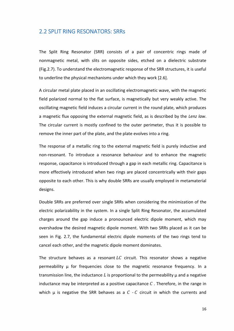
2.2 SPLIT RING RESONATORS: SRRs
The Split Ring Resonator (SRR) consists of a pair of concentric rings made of
nonmagnetic metal, with slits on opposite sides, etched on a dielectric substrate
(Fig.2.7). To understand the electromagnetic response of the SRR structures, it is useful
to underline the physical mechanisms under which they work [2.6].
A circular metal plate placed in an oscillating electromagnetic wave, with the magnetic
field polarized normal to the flat surface, is magnetically but very weakly active. The
oscillating magnetic field induces a circular current in the round plate, which produces
a magnetic flux opposing the external magnetic field, as is described by the Lenz law.
The circular current is mostly confined to the outer perimeter, thus it is possible to
remove the inner part of the plate, and the plate evolves into a ring.
The response of a metallic ring to the external magnetic field is purely inductive and
non-resonant. To introduce a resonance behaviour and to enhance the magnetic
response, capacitance is introduced through a gap in each metallic ring. Capacitance is
more effectively introduced when two rings are placed concentrically with their gaps
opposite to each other. This is why double SRRs are usually employed in metamaterial
designs.
Double SRRs are preferred over single SRRs when considering the minimization of the
electric polarizability in the system. In a single Split Ring Resonator, the accumulated
charges around the gap induce a pronounced electric dipole moment, which may
overshadow the desired magnetic dipole moment. With two SRRs placed as it can be
seen in Fig. 2.7, the fundamental electric dipole moments of the two rings tend to
cancel each other, and the magnetic dipole moment dominates.
The structure behaves as a resonant 𝐿𝐶 circuit. This resonator shows a negative
permeability µ for frequencies close to the magnetic resonance frequency. In a
transmission line, the inductance 𝐿 is proportional to the permeability µ and a negative
inductance may be interpreted as a positive capacitance 𝐶 . Therefore, in the range in
which µ is negative the SRR behaves as a 𝐶 - 𝐶 circuit in which the currents and

17
voltages cannot propagate along the line, having instead an evanescent behaviour,
consistent with their electromagnetic counterpart, as previously anticipated [2.1].
2.2.1 Electromagnetic resonances in individual SRR
In order to optimize the use of SRR, the accurate estimation of the SRR resonant
frequency is imperative. There are several analytical models in literature studying the
resonance of SRRs. In this thesis work the resonance evaluation is derived from the
formula given by C. Saha et al. [2.7] for a square split ring resonator (Fig.2.8).
Figure 2.8 – [2.7] Schematic view of a square SRR
The structure behaves as a 𝐿𝐶 circuit having resonance frequency 𝑓0 given by:
𝑓0 =
1
2𝜋
1
√𝐿𝑇𝐶𝑒𝑞
(2.21)
where 𝐿𝑇 is the total inductance and 𝐶𝑒𝑞 is the total equivalent capacitance, reported
in [2.7]. The total equivalent capacitance of the SRR has two contributions, one arising
from the splits and the other one from the gap between the concentric rings. The
inductances arise from the conducting rings and gap between inner and outer rings.
𝐿𝑇 and 𝐶𝑒𝑞, and then 𝑓0, strongly depend on the SRR dimensions, in particular the
resonance frequency increases when the side of the outer ring decreases.
For an individual SRR, both electric and magnetic fields can induce resonances, the
magnetic one being the strongest. P.Gay-Balmaz and O.J.Martin [2.8] investigated the

18
SRR response illuminated with a plane wave propagating in the 𝒌 direction and with
different field orientations (Fig.2.9):
a) 𝑬 parallel to the gap and 𝑯 parallel to the rings axis (parallel polarization);
b) 𝑬 parallel to the gap and 𝑯 perpendicular to the rings axis (perpendicular
polarization);
c) 𝑬 perpendicular to the gap and 𝑯 parallel to the rings axis (parallel
polarization);
d) 𝑬 perpendicular to the gap and 𝑯 perpendicular to the rings axis
(perpendicular polarization).
Figure 2.9 – [2.8] The SRR is illuminated with a plane wave propagating in the k direction and two different illumination polarizations are considered: parallel polarization (H parallel to the SRR z axis), and perpendicular polarization, (H normal to the SRR z axis) .Two different SRR arm orientations with respect to E are investigated.
The article reports that the resonant behaviour of the SRR is analysed placing the Split
Ring in the middle of an R9 rectangular waveguide and the scattering parameters
measured using a Network Analyzer2. The strongest resonance is observed for parallel
polarization (a), for the perpendicular polarization (b) a much weaker resonance is
observed. If the SRR is rotated vertically around its z axis, the resonance for parallel
polarization (c) is unaffected , while the resonance for perpendicular polarization (d) is
completely suppressed (Fig.2.10).
2 The Vector Network Analyzer operation is described in the Chapter 4

19
Figure 2.10 – [2.8] Scattering parameter S21 measured in a R9 waveguide for a single SRR illuminated in the configuration and polarizations of Fig.2.9.
2.2.2 Magnetic resonance for different SRR parameters
To optimize the SRR resonance frequency, it is possible to change some structure
parameters, taking into account that a SRR behaves as a 𝐿𝐶 circuit (Eq.2.21). The
geometrical parameters investigated by K. Aydin et al. [2.9] are: the outer ring side, the
split width, the gap between the rings, the metal width, respectively 𝑔, 𝑑, 𝑐 in Fig.2.8
and the split number.
Outer ring side
Increasing the outer ring side, the space in which is possible to trap a resonance
mode, and thus its wavelength, increases. For larger side therefore the
resonance frequency of the SRR decreases.
Split width
The splits behave like a parallel plate capacitor placed with a distance 𝑔
between them. Increasing the split width, the capacitance due to splits will
decrease, lowering the total capacitance of the system and in turn increasing
the resonance frequency of the SRRs.

20
Gap between the rings
Changing the distance between the inner and outer rings will change the
mutual capacitance and mutual inductance between the rings. Increasing the
gap distance will decrease both the mutual capacitance and mutual inductance
of the equivalent 𝐿𝐶 circuit of SRR system, and consequently the resonance
frequency increases.
Metal width
Metal width affects all capacitances and inductances. Fixing the outer ring
radius and increasing the metal width will decrease the mutual inductance and
mutual capacitance. Therefore, SRRs made of thinner rings will have smaller
resonant frequencies.
Split number
Increasing the number of splits increases the number of capacitances in series,
thus decreases the total capacitance of the system and in turn increases the
resonance frequency of the SRR.
2.2.3 Interacting Split Ring Resonator
P.Gay-Balmaz and O.J.Martin [2.8] studied the interaction of several SRRs as a function
of their geometrical arrangement, placing the structures in a waveguide.
They first considered a row of parallel SRRs placed along an horizontal line (Fig.2.11)
with a distance between the resonators axis equal to 𝑑 =𝜆𝑚
4 , where 𝜆𝑚 is the
wavelength corresponding to the mode propagating in the waveguide, at the
resonance frequency of the SRRs. Each additional SRR, at the same distance, decreases
the transmitted power but this effect remains strongly frequency selective (figure
2.11). The separation distance 𝑑 between two SRRs is varied. When 𝑑 decreases from
𝜆𝑚
2 to
𝜆𝑚
4, the coupling increases and the transmitted power decreases. For a shorter
separation two resonances appear (Fig.2.11).

21
Figure 2.11 – [2.8] (Left) the scattering parameter S21 measured for one, two, three, and four SRRs placed along a line; (Right) scattering parameter S21 measured for two SRRs in a row for different separation distance d.
When additional rows of SRRs are added along the SRRs axis direction, the resonance
frequency is shifted to lower values and the additional frequency shift, for a shorter
separation, decreases when more SRR rows are added. The inter-row spacing e also
influences the resonances. For small spacing the resonance shifts towards lower
frequencies and becomes narrower (Fig.2.12).
Figure 2.12 – [2.8] (Left) Scattering Cross Section computed for 1,2 and 3 rows of SRRs resonators, two different separation distances d have been selected. (Right) Scattering Cross Section computed for different distance e between the rows.

22
Placing two SRRs side by side (Fig.2.13) it is possible to have a broader resonance
frequency and when the lateral separation distance c decreases the resonance
frequency shifts towards lower values, as in the case of longitudinal separation.
Figure 2.13 – [2.8] Scattering Cross Section computed for different lateral separation
distances c.

23
2.3 ULTRA-BROADBAND METAMATERIAL ABSORBER
Several advanced artificial elements for magnetic metamaterials include arrays of pairs
of metallic cut-wire, plates or strips. Each of these structures is capable of supporting a
principal eigenmode with anti-symmetric current distribution in the coupled system, in
order to obtain a magnetic dipole.
In 2005, negative effective permeability from square nano-plate pair arrays, has been
observed by G. Dolling et al. [2.10]. They illustrate the connection between normal
SRRs and cut-wire pairs (Fig.2.14), subsequently they investigate sample for which the
wire width is equal to the wire length, in order to reduce the polarization dependence
of the cut-wire pairs: the cut-wire pairs turn into plate pairs.
Figure 2.14 – [2.10] Schematic of the adiabatic transition from split-ring resonators to cut-wire pairs as magnetic atoms.
By simply extending the pairs of rods along the direction of the external magnetic field
H, pair of strips is obtained, and a structure such as that shown in Fig.2.15 is
achievable. The basic structure of the nanostrip magnetic metamaterial consists of a
pair of metallic nanostrips spaced by a dielectric layer.
Figure 2.15 – Schematic of the structure consisting of coupled nanostrips.

24
These strips support asymmetric currents in the metalic structures induced by the
perpendicular magnetic field and exhibit both magnetic and electric resonances under
a TM illumination, with the magnetic field polarized along the strips.
The breakthrough obtained by these kind of materials, compared to the SRRs, is a
multi-frequencies resonant mode [2.11].
In many cases, metamaterials resonance is utilized in the process of absorption but the
absorption bandwidth is often narrow, typically no larger than 10% with respect to the
central frequency. A broadband absorption is often required, as in this thesis work. An
effective model to extend the absorption band is to make the metamaterial unit
resonate at several neighboring frequencies. A pyramidal structure that consists of
metal patches with their width tapered linearly from the top to the bottom is able to
extend the absorption band. The electromagnetic field is resonantly localized and then
absorbed at some part of the pyramids. At a smaller frequency, it is localized at the
bottom side and as the frequency increases, the localized electromagnetic field moves
gradually towards the top-side (Fig.2.16). The collection of the resonance at different
frequencies results in an ultra-broadband absorption.
Figure 2.16 – [2.11] (Left) Pyramidal structure that consists of square metal patches with linearly tapered width from the top to the bottom, able to extend the absorption band.(Right) The localized electromagnetic field moves gradually towards the top-side, increasing the frequency; (a) (c) (e) (g) for the electric amplitude, (b) (d) (f) (h) for the magnetic amplitude.

25
CHAPTER 3
LHC,IMPEDANCE AND TCT COLLIMATOR
3.1 THE CERN LARGE HADRON COLLIDER: LHC
In 1954 the European Organization for Nuclear Research (CERN) was founded, with the
aim of establishing a world-class physics research organization in Europe. The main
important purview in which this organization works is the high-energy physics and, for
this purpose, provides the particle accelerators and other necessary infrastructure.
The CERN is located at the French-Swiss border and counts 22 Members States, 10
“Observers” and provides facilities to 600 institutes and universities involving 90
nationalities.
The latest addition to CERN’s accelerator complex is the Large Hadron Collider (LHC),
the world’s largest and most powerful particle accelerator, reaching 14 TeV at the
collision point. It has been completed on July 2008 and tested for the first time on
September 10, 2008 with its first circulating beam. The LHC consists of a 27-kilometre
ring that crosses the border between Switzerland and France, at a depth ranging from
50 to 175 meters underground. Inside the accelerator, two high-energy protons beams
travel in opposite directions in separate beam pipes, two tubes kept at ultrahigh
vacuum, before they are made to collide. A description of the LHC accelerator complex
is shown in Fig.3.1 and briefly described in the following.

26
Figure 3.1 – CERN accelerator complex
The proton source is a simple bottle of hydrogen gas. An electric field is used to strip
hydrogen atoms of their electrons to yield protons. Linac2, the first linear accelerator
in the chain, accelerates the protons to the energy of 50 MeV. The beam is then
injected into the Proton Synchrotron Booster (PSB), which accelerates the protons to
1.4 GeV, followed by the Proton Synchrotron (PS), which pushes the beam to 25 GeV.
Protons are then sent to the Super Proton Synchrotron (SPS) via TT2 and TT10 transfer
lines, where they are accelerated to 450 GeV. The protons are finally transferred to the
two beam pipes of the Large Hadron Collider (LHC) via TT60/T12 and TT40/T18 transfer
lines.
The general LHC technical data are summarize in Table 3.1 [3.1]. Inside the LHC beam
pipes, one beam circulates clockwise in one pipe while the other one circulates
anticlockwise in the second pipe. The beams are guided around the accelerator ring by
a strong magnetic field maintained by different superconducting magnets. 1232 dipole
magnets keep the beams on their circular path. The technical data regarding the dipole
magnets are summarized in Table 3.2 [3.1]. Additional 392 quadrupole magnets are
used to keep the beams focused, in order to maximize the chances of interaction

27
between the particles in four intersection points. These locations correspond to the
position of four particle detectors: ATLAS, CMS, ALICE and LHCb, where the total
energy at the collision point is equal to 14 TeV. At this energy, the protons have a
Lorentz factor of about 7500 and move at about 99.9999991% of the speed of light. It
will take less than 90 μs for a proton to travel once around the main ring (a frequency
of about 11000 revolutions per second). Rather than continuous beams, the protons
will be bunched together, into 2808 bunches, so that interactions between the two
beams will take place at discrete intervals never shorter than 25 ns. Approximately 96
tons of liquid helium are needed to keep the over 1600 magnets (with most weighing
over 27 tonnes) at their operating temperature, making the LHC the largest cryogenic
facility in the world at liquid helium temperature.
Table 3.1 [3.1] - General LHC technical data
Injection Energy 450 GeV
Maximum proton kinetic energy 7 TeV
Energy loss per turn 6.7 keV
Tunnel circumference 27 km
Number of bunches around ring 2808
Number of particles per bunch 1.1 × 10¹¹
Circulating current per beam 0.54 A
Bunch spacing 25 ns
Maximum proton velocity 0.99999991c

28
Table 3.2 [3.1] - Data regarding the dipole magnets
Number of dipole magnets 1232
Bending Radius 2803.928 m
Length of each dipole magnet 4.3 m
Strength of dipole magnets 8.33 T
Bending angle per magnet 5.1000 mrad
Field at injection 0.535 T
Current at injection (0.45 TeV) 739 A
Nominal current 1850 A
Peak field in coil 8.76 T
Operating Temperature 1.9 K

29
3.2 THE LHC COLLIMATION SYSTEM [3.2]
Partial or total beam losses are unavoidable in particle accelerators. In order to reduce
and check the losses in the LHC accelerator, a collimation system has been developed.
As it has been anticipated above, the protons are bunched together. In the transverse
plane, the bunched particle beams are generally characterized by a parabolic
distribution but no lack of validity is found if a Gaussian-like distribution of particles is
assumed for the analysis of the collimation system. Looking at the standard deviation
of the Gaussian distribution, the beam core (97% of all particles) is defined as 0-3σ,
while the region >3σ is defined as the beam halo.
Figure 3.2 – Core and halo for a particle beam with Gaussian transverse particle distribution
Several effects give rise to an increase of the beam halo population and consequently
the beam losses. The following relation describes the time-dependent beam intensity:
𝐼(𝑡) = 𝐼0 𝑒
−𝑡
𝜏𝑏 (3.1)
where 𝜏𝑏 is the machine cycle. Thus the particle loss rate is

30
−
1
𝐼0
𝑑𝐼
𝑑𝑡=
1
𝜏𝑏 (3.2)
At 7 TeV 1% only of total beam intensity loss in a period of 10s would produce a peak
load of 500 kW, whereas the upper limit to superconducting magnets (SC) energy
deposition, without quench, is ≈ 8.5 W/m.
Collimation system has been designed to monitor the losses, with the aim to clean the
beam halo in each cycle and thus to protect the SC magnets against the quenching
and the structure against the power radiation. The goal to have all losses at collimators
requires to place the collimators where the amplitude of the particle oscillations are
growing. They are placed around the beam with various settings of longitudinal and
transversal positions. In Figure 3.3 it is possible to see the collimator layout in the LHC
machine.
Figure 3.3 – Collimator layout in the LHC machine.

31
Generally a collimator is made of two parallel jaws that define a slit for the beam
passage that can be larger or smaller depending on the jaws distance (gap). The
collimator whole box can be rotated, translated or skewed. According to the jaws
materials, the collimation system owns a well-defined hierarchy: low Z materials, like
Carbon Fiber Composite (CFC), are used to protect the machine against primary and
secondary radiation fields. For these reasons they are called respectively Primary
Collimator (TCP) and Secondary Collimators (TCS). While, higher Z materials, like
Tungsten (W), are used to intercept the tertiary radiation and the hadronic showers
produced by the interaction of the primary proton beam halo. This kind of collimators
is called Tertiary (TCT) and it will be better analyzed in the Paragraph 3.4. The
collimators hierarchy is shown in Figure 3.4. Another kind of collimator is the Injection
Collimator (TDI) that have an important role for the local protection against injection
failures. Some specifications about the primary, secondary and tertiary collimators are
shown below in Tables 3.3 and 3.4.
Figure 3.4 – LHC Collimation hierarchy. Low Z materials (CFC) used to protect the machine against primary and secondary radiation fields. High Z materials (W/Cu), used to intercept the tertiary radiation and the hadronic showers produced by the interaction of the primary proton beam halo.

32
Table 3.3 - General primary collimator (TCP) and secondary collimator (TCS) parameters.
PARAMETER TCP TCS
Jaw material CFC CFC
Jaw length [cm] 60 100
Jaw tapering [cm] 10+10 10+10
Jaw cross section [mm2] 65∙25 65∙25
Jaw resistivity [μΩm] ≤ 10 ≤ 10
Heat load [kW] ≤ 7 ≤ 7
Jaw temperature [°C] ≤ 50 ≤ 50
Residual vacuum pressure [mbar ] ≤ 4∙ 10-8 ≤ 4∙ 10-8
Gap range [mm] 0.5÷58 0.5÷58
Maximum jaw angle [mrad] 2 2
Table 3.4 – Some Specifications for other LHC ring collimators.
PARAMETER TCT TCLA TCL TCLP TCLI
Jaw material W W Cu Cu CFC
Jaw length [cm] 100 100 100 100 100
Jaw tapering [cm] 10+10 10+10 10+10 10+10 10+10
Minimal gap [mm] ≤0.8 ≤0.8 ≤0.8 ≤0.8 ≤0.5
The collimation system, though necessary to protect the accelerator structure, is itself
an important instability source. When the collimators are moved very close to the
circulating beam, new electromagnetic fields are generated which can cause
perturbations to the main fields. Thus the LHC collimation system is a critical element

33
for the safe operation of the LHC machine and it is subject to continuous performance
monitoring, hardware upgrade and optimization.
In order to describe and to monitor the instability due to the collimation system, the
Impedance and Wakefield concepts will be introduced in the following paragraph.

34
3.3 BEAM COUPLING IMPEDANCE
In an accelerator the electromagnetic interaction between the beam and the
surrounding equipment represents an important contribution in the coherent
instabilities study. This phenomenon limits the accelerator performance and needs to
be taken into account in the design of the machine. The strength of the interaction is
characterized by the Beam Coupling Impedance of the accelerator components in the
frequency domain and by the Wakefield in the time domain [3.3].
The need to evaluate the Beam Coupling Impedance, in order to ensure the beam
stability in the circular accelerators, was born with the achievement of high current
intensity in the collider accelerators. To understand this assertion it can be useful to
describe the electromagnetic problem inside the circular accelerator as summarized in
Figure 3.5.
Figure 3.5 – Electromagnetic Problem Scheme
The beam is initially driven by external electromagnetic fields (𝑬, 𝑯) due to magnets
and accelerating cavities and is characterized by unperturbed current and charge
density (𝑱, 𝜌). In reality, perturbed charge and current density are added to the
unperturbed ones. It is possible to identify a transfer function between the original
fields and the perturbed charge and current density, which has the dimension of the
inverse of an impedance [𝐼/𝑉]. It is indicated with (𝑍𝐷)−1 , where the subscript D stay
for Dynamic and indicates the bond between this function and the original beam
dynamic. This quantity is intrinsic to the beam and to the machine equipment.

35
The new current and the new charge density (𝑱∗, 𝜌∗), sum of the unperturbed and
perturbed one, generate new electric and magnetic fields depending on the boundary
conditions given by the structure in which the beam propagates. The original
Maxwell’s equations are modified and the original beam is perturbed. At this point, it
is possible to introduce a new transfer function between the perturbed charge and
current density and the new electromagnetic field. It is called Beam Coupling
Impedance 𝑍 and depends on the surrounding equipment of the machine.
The beam coupling impedance 𝑍 must be kept below a certain threshold and in
particular, it must be contained in a stability region, defined by 𝑍𝐷 in order to reduce
the perturbation of the beam. In the old fixed target accelerators, the low intensity
current generated a wide stability region, 𝑍𝐷 ∝ (𝐼)−1, thus the beam coupling
impedance reduction was not necessary. With the high intensity current achievement,
the evaluation of this kind of impedance has become mandatory.
3.3.1 Wake field [3.2]
Generally the charged particle motion in the accelerator, is due to an external
electromagnetic field (𝑬, 𝑩) and is governed by the Lorentz force:
𝑭 = 𝑚0𝛾
𝑑𝒗
𝑑𝑡= 𝑞(𝑬 + 𝒗 × 𝑩) (3.3)
where 𝛾 is the Lorentz energy factor 𝛾 = 1/√1 − 𝛽2 , 𝛽 = 𝑣/𝑐.
However the charged particle itself generates an electric and magnetic field. In the free
space, it is possible to distinguish three cases, listed and shown below, with regard to
the generated electric field:
a) If the charge is stationary, its electric field lines radiate outwards isotropically;
b) if the charge moves relativistically with velocity 𝑣 ≈ 𝑐, being the velocity of
light in the free space, electric field lines get contracted into a thin disk,
perpendicular to the particle direction of motion with an angular spread of 1
𝛾 ;

36
c) if the charge moves in ultrarelativistic limit 𝑣 = 𝑐, then the disk reduces to a δ-
function thin sheet.
Figure 3.6 – Electric field lines generated by a charged particle in free space in the stationary case (a), moving relativistically (b) and in the ultrarelativist limit (c).
Magnetic field is also generated by a moving particle but with different properties. It
also get contracted into a thin disk as 𝑣 approaches 𝑐, but its direction is azimuthal
instead of radial as the electric field direction. A cylindrical coordinate system to
describe the particle motion in free space is chosen, (𝑟, 𝜃, 𝑠), in which 𝑠 is the absolute
longitudinal charged particle position, in the laboratory frame. The application of the
Gauss’s law for the electric field and of the Ampere’s law for the magnetic field defines
the following relations for the electric and magnetic fields generated by the charged
particle in the ultrarelativistic limit:
𝐸𝑟 =2𝑞
𝑟𝛿(𝑠 − 𝑐𝑡) (3.4)
𝐵𝜃 =2𝑞
𝑟𝛿(𝑠 − 𝑐𝑡) (3.5)
When the particle motion is realized along the axis of an ideal3 vacuum chamber pipe,
the equations 3.4 and 3.5 are still true, but with the field lines perfectly terminating on
the pipe wall. Moreover, an image charge is generated on the wall, exactly equal and
opposite to the particle, moving with the same velocity 𝑣 = 𝑐, in the same direction
and no field is left behind. This situation is not described by two particles moving side
3 An ideal vacuum chamber is defined as an axially symmetric structure with perfectly conducting wall.

37
by side exactly at the same longitudinal position. Fortunately, in this case electric and
magnetic fields mutually cancel and no Lorentz force on the particles is exercised.
When the vacuum chamber presents a discontinuity, the image charges moving along
the pipe have now to move around a corner and, as the electromagnetic theory
establishes, due to the banding it radiates. Thus additional electromagnetic fields are
generated. Because of causality, such fields called wake fields exist behind the particle
and will perturb the motion of the following particle, called witness. Thus, a real
particle experiences an “effective” electromagnetic field given by the sum of the one
produced by the external lattice elements of the accelerator, and the other being the
wakes produced by the particles in front interacting with the vacuum chamber:
(𝑬, 𝑩)𝑒𝑓𝑓𝑒𝑐𝑡𝑖𝑣𝑒 = (𝑬, 𝑩)𝑒𝑥𝑡𝑒𝑟𝑛𝑎𝑙 + (𝑬, 𝑩)𝑤𝑎𝑘𝑒𝑠 (3.6)
Figure 3.7 – a) Charged beam passing through an ideal beam pipe, no wake field is generated; b) Charged beam passing through a beam pipe with discontinuities, wake field is generated.
The wake field can be considered as a perturbation if (𝑬, 𝑩)𝑤𝑎𝑘𝑒𝑠 ≪ (𝑬, 𝑩)𝑒𝑥𝑡𝑒𝑟𝑛𝑎𝑙.
In the perfectly conducting vacuum chamber walls, the wake field is due only to
structure discontinuities and it is called geometric wake field. In a vacuum chamber
with finite constant electric conductivity σ walls, the so called “resistive wall wake
fields ” (RW) are generated.
Electric and magnetic fields are driven by charges and currents respectively. In the case
of metals, charges stay on the surface and are not allowed to enter inside, whereas
currents stay near the surface and penetrate into the conductor. The parameter
quantifying how much they penetrate is the skin depth:

38
𝛿𝑠𝑘𝑖𝑛 = 𝑐
√2𝜋𝜎|𝜔| (3.7)
where σ is the finite conductivity of the metal and ω the frequency of the
electromagnetic field. Thus both electric and magnetic field give rise to RW wake
fields. In the case of RW wake fields, the magnetic fields mainly contribute to
transverse wake force, while the associated electric field contributes to longitudinal
wake force.
3.3.2 Wake field and Impedance: Longitudinal Plane [3.4]
Starting from the concepts described in the previous paragraph, it is possible to
introduce the longitudinal impedance concept and its link to the longitudinal wake
field.
Let’s image a single particle q1 going through a device and a second probe particle q
behind the first one with the same velocity v=βc. In the figure 3.8 is shown the
coordinates system where (𝒓𝟏, 𝑧1) and (𝒓, 𝑧) are the transverse position and the
longitudinal vector position for the charge q1 and q respectively.
Figure 3.8 – Coordinate System

39
The particle q feels the oscillating field that q1 leaves behind and thus, it will be subject
to a force due to the q1 field. The Lorentz force acting on the charge q at a given
position 𝒓 is:
𝐹(𝒓, 𝑧, 𝒓𝟏, 𝑧1; 𝑡) = 𝑞 [ 𝐸(𝒓, 𝑧, 𝒓𝟏, 𝑧1; 𝑡) + 𝒗 × 𝑩(𝒓, 𝑧, 𝒓𝟏, 𝑧1; 𝑡)] (3.8)
which has in general field components along and perpendicular to the trajectory. At
any instant 𝑡, the leading and trailing charges have longitudinal coordinates 𝑧1(𝑡) = 𝑣𝑡
and 𝑧(𝑡) = 𝑣(𝑡 − 𝜏) respectively, where 𝜏 is the time delay of the trailing charge with
respect to the leading one. The energy lost by the charge q1 is computed as the work
done by the longitudinal electromagnetic force along the structure:
𝑈11(𝒓𝟏) = − ∫ 𝐹
∞
−∞
(𝒓𝟏, 𝑧1, 𝒓𝟏, 𝑧1; 𝑡) 𝑑𝑧 (3.9)
Where 𝑡 =𝑧1
𝑣 and 𝑈11 is the energy lost by the particle q1 in the resistive walls and in
the diffracted radiated fields, caused by the discontinuities of the vacuum pipe.
Generally it is a positive quantity (energy loss).
The particle q also changes its energy under the effect of the fields produced by the
leading particle q1:
𝑈21(𝒓, 𝒓𝟏, 𝜏) = − ∫ 𝐹
∞
−∞
(𝒓, 𝑧, 𝒓𝟏, 𝑧1; 𝑡) 𝑑𝑧 (3.10)
Where 𝑡 =𝑧1
𝑣+ 𝜏 and q and q1 are on the same path but with the time delay 𝜏. 𝑈21
can be positive (energy loss) or negative (energy gain) and the magnetic field cannot
change the particle energy because the product 𝒗 × 𝑩 ∙ 𝑑𝒛 = 0. Accordingly, the
energy gain is computed considering the longitudinal component of the electric field
only.
In the real case, the path of integration in (3.9) and (3.10) is not infinite, because the
field is confined in a limited region. However, the integrals in (3.9) and (3.10) are a
good approximation as long as the field wavelength is short compared to the device
length. Moreover, it has been assumed the charge velocity unchanged during the
motion, as in the case, for instance, of ultra-relativistic charges.

40
Starting from (3.9) and (3.10) it is possible to define two quantities, the loss factor 𝑘
that is the energy lost by q1 per unit charge squared:
𝑘(𝒓𝟏) [
𝑉
𝐶] =
𝑈11(𝒓𝟏)
𝑞12 (3.11)
and the longitudinal wake function 𝑤𝑧(𝑟, 𝑟1; 𝜏), the energy lost by the trailing charge q
per unit of both charges q1 and q:
𝑤𝑧(𝒓, 𝒓𝟏; 𝜏) [
𝑉
𝐶] =
𝑈21(𝒓, 𝒓1; 𝜏)
𝑞𝑞1 (3.12)
In literature the quantity 𝑤( 𝜏 ) is sometimes unproperly called wake potential; the
wake function is numerically equal to the potential seen by the charge only when one
considers unity charges. From the above definitions it is visible that, when the charges
travel on the same trajectory, the loss factor is given by the wake function in the limit
of zero distance between q1 and q, 𝑘 = 𝑤𝑧(0). This is generally true as long as β < 1;
however, in the relevant case β = 1 it has been proved that
𝑘 =
𝑤𝑧(𝜏 → 0+)
2 (3.13)
In fact, due to the finite propagation velocity of the induced fields and to the motion of
the source charge, the wake function is not symmetric with respect to the leading
charge and it exists only in the region τ>0, showing a discontinuity at the origin.
Figure 3.9 – Longitudinal wakefield in the relativistic (β<1) and ultra-relativistic case (β=1).

41
The wake function defined in (3.12) is generated by a point charge thus it is a Green
function and allows to compute the wake produced by any bunch distribution with a
longitudinal time distribution function 𝐢𝐛(𝛕), such that :
𝑞1 = ∫ 𝑖𝑏(𝜏)𝑑𝜏
+∞
−∞
(3.14)
The wake function produced by the bunch distribution at a point with time delay τ is
simply given by the convolution of the Green function over the bunch distribution,
where the convolution integral is obtained by splitting the distribution into an infinite
number of infinitesimal slices and sum up their wake contributions at the point τ.
Moreover, the energy lost by a trailing charge q because of the wake produced by the
slice at τ' is:
𝑑𝑈(𝒓, 𝜏 − 𝜏′) = 𝑞 𝑖𝑏(𝜏′)𝑤𝑧(𝒓, 𝜏 − 𝜏′)𝑑𝜏′ (3.15)
Summing up all the effects, it is possible to define the wake function of a bunch
distribution as:
𝑊𝑧(𝒓, 𝜏) =
𝑈(𝒓, 𝜏)
𝑞𝑞1=
1
𝑞1∫ 𝑖𝑏(𝜏′)𝑤𝑧(𝒓, 𝜏 − 𝜏′)𝑑𝜏′
+∞
−∞
(3.16)
and consequently the loss factor of the charge distribution
𝐾(𝒓) =
𝑈(𝒓)
𝑞12 =
1
𝑞1∫ 𝑊𝑧(𝒓, 𝜏)𝑖𝑏(𝜏)𝑑𝜏
+∞
−∞
(3.17)
It is possible describe the wake field as a transfer function in the frequency domain
that defines the longitudinal beam coupling impedance of the element under study:
𝑍||(𝒓, 𝒓𝟏, 𝜔)[𝛺] = ∫ 𝑊𝑧(𝒓, 𝒓𝟏; 𝜏)𝑒𝑖𝜔𝜏𝑑𝜏+∞
−∞
(3.18)
where 𝜔 = 2𝜋𝑓 is the angular frequency conjugate variable of the time delay 𝜏 =𝑧
𝑣 .
The beam coupling impedance is a complex quantity
𝑍(𝜔) = 𝑍𝑟(𝜔) − 𝑖𝑍𝑖(𝜔) (3.19)

42
where 𝑍𝑟 and 𝑍𝑖 are even and odd function of 𝜔 respectively. Recalling the relation
(3.13), it is possible to obtain:
𝑘 =
𝑤𝑧(𝜏 → 0+)
2=
1
𝜋∫ 𝑍𝑟(𝜔) 𝑑𝜔
∞
0
(3.20)
where the wake function is derived from the impedance by inverting the Fourier
integral and the real part of the impedance is the power spectrum of the energy loss of
a unit point charge. In general, the complex impedance can be seen as the complex
power spectrum related to the energy loss.
3.3.3 Wake field and Impedance: Transverse Plane [3.4]
In Figure 3.8 the charge q experiences a Lorentz force which has longitudinal and
transverse components. Therefore, it is subject to a transverse momentum kick that
depends on the pipe shape and on the transverse position of both charges.
𝑀2,1(𝒓, 𝒓1; 𝜏)[𝑁𝑚] = ∫ 𝐹┴(𝒓, 𝑧, 𝒓𝟏, 𝑧1
+∞
−∞
; 𝑡)𝑑𝑧 (3.21)
where 𝑡 =𝑧1
𝑣+ 𝜏. In general, the transverse kick is not parallel to the displacement of
the leading charge. In fact an horizontal displacement can lead to both vertical and
horizontal kicks, and the same generally happens for a vertical displacement. Only in
the case of cylindrical symmetry, the two transverse directions are de-coupled for a
beam on the axis. The transverse kick per unit of both charges defines the transverse
wake function:
𝑊┴(𝒓, 𝒓𝟏, 𝝉)[𝑉 𝐶⁄ ] =
𝑀2,1(𝒓, 𝒓1; 𝜏)
𝑞1𝑞 (3.22)
Analogously to the longitudinal case, it is possible to define the dipole transverse loss
factor as the amplitude of the transverse momentum kick given to the charge by its
own wake per unit charge:

43
𝑘┴(𝒓𝟏)[𝑉 𝐶⁄ ] =
𝑀1,1(𝒓1)
𝑞12
(3.23)
Usually the dipole component of the transverse kick is the dominant term for ultra-
relativistic charges. This term is proportional to the displacement of the charge q1.
The transverse wake potential produced by a continuous bunch distribution,
transversely displaced by 𝒓, can be obtained by applying the superposition principle.
𝑊┴(𝒓; 𝜏)[𝑉 𝐶⁄ ] =
1
𝑞1∫ 𝑖𝑏(𝜏′)𝑤┴(𝒓, 𝜏 − 𝜏′)𝑑𝜏′
+∞
−∞
(3.24)
And the bunch transverse loss factor is:
𝐾┴(𝒓) =
1
𝑞1∫ 𝑊┴(𝒓, 𝜏)𝑖𝑏(𝜏)𝑑𝜏
+∞
−∞
(3.25)
Likewise to the longitudinal case, the transverse beam coupling impedance of the
element understudy is defined as the Fourier transform of the respective wake
function:
𝑍┴(𝒓, 𝒓2, 𝜔)[𝛺] = −𝑖 ∫ 𝑊┴(𝒓, 𝒓2, 𝜏)𝑒𝑖𝜔𝜏𝑑𝜏+∞
−∞
(3.26)
Where, historically, the imaginary constant was introduced in order to make the
transverse impedance to play the same role as the longitudinal one in the beam
stability theory, since the transverse dynamics is dominated by the dipole transverse
wake.
3.3.4 Resonator Impedance
Cavity structures usually show an impedance behaviour in frequency consisting of
many resonant peaks, mainly due to trapped modes. These are electromagnetic field
resonances with frequencies below the lowest cut-off frequency of the beam pipe.
Each resonance can be approximated using a parallel RLC circuit.

44
The admittance of such a circuit can be easily calculated from the elementary circuit
theory as:
𝑌(𝜔) =
1
𝑅− 𝑖𝜔𝐶 +
𝑖
𝜔𝐿 (3.27)
where 𝑅 is the resistance, 𝐶 is the capacitance and 𝐿 is the inductance. If the AC
voltage across the parallel resonant circuit is 𝑉, then the complex power delivered to
the resonator is:
𝑃𝑖𝑛 =
|𝑉2|
2𝑌(𝜔) =
|𝑉2|
2(
1
𝑅− 𝑖𝜔𝐶 +
𝑖
𝜔𝐿) (3.28)
At resonance, the reactive power of the inductor is equal to the reactive power of the
capacitor. Therefore, the power delivered to the resonator is equal to the power
dissipated in the resistor.
𝑃𝑖𝑛 =
|𝑉2|
2𝑅 (3.29)
where 𝑅 usually is recognized as the shunt impedance 𝑅𝑠 and represent the quantity to
be optimized in order to minimize the power required for a given voltage.
Calling 𝜔𝑟 the resonance frequency for the parallel resonant circuit:
𝜔𝑟 = 2𝜋𝑓𝑟 =
1
√𝐿𝐶 (3.30)
from Eq. 3.27 the complex impedance of the parallel resonator circuit directly follows:
𝑍(𝜔) =
𝑅𝑠
1 − 𝑖𝑄 (𝜔𝜔𝑟
−𝜔𝑟
𝜔 ) (3.31)
where 𝑄 = 𝑅𝑠√𝐶
𝐿 is the resonant quality factor. This parameter can be shown to be the
ratio of the energy stored in the inductor and capacitor to the power dissipated in the
resistor as a function of frequency.
When 𝜔 = 𝜔𝑟 the impedance is purely real and reaches the maximum 𝑅𝑒{𝑍} = 𝑅𝑠
whereas the imaginary part vanishes. The Full Width at Half Maximum of the
resonance peak is defined as the resonance bandwidth 𝛥𝜔, related to 𝑄 by 𝑄 = 𝜔𝑟
𝛥𝜔. For
𝜔 → 0, the real part of the impedance vanishes quadratically and the impedance is
purely imaginary reactive. The real part of the impedance is always positive. When the

45
wall resistivity increases 𝑄 decreases, the shunt impedance being inversely
proportional to the wall resistivity, the impedance also decreases.
For cavities made of good metallic conductors, usually 𝑄 ≫ 100, and the impedance
shows many well distinguishable resonant peaks, due to parasitic Higher Order Modes
(HOMs), narrow-band impedance. Each resonance is produced by a localized mode
whose frequency is below or not much above the cut-off frequency of openings
present in the structure. In the time domain, this corresponds to a slowly decaying
oscillating wake potential. Above the cut-off frequency, in the high frequency region,
the resonances overlap producing a smooth frequency dependence of the impedance
(Fig.3.10). In the time domain, this corresponds to the short-range behaviour of the
wake potential.
As mentioned before the high frequency coupling impedance describes the interaction
of particles due to the abrupt changes of the beam pipe cross sections and/or due to
high frequency tails of resonances. In this context, the role of the bunch length with
respect to the beam pipe radius is important. If the bunch length is larger than the
beam pipe radius, the detailed behaviour of the high-frequency impedance can be
approximated by a smooth function generally referred to as broad-band impedance. If
the bunch length is small compared to the beam pipe radius, as in the case of new
colliders, the high-frequency impedance becomes more significant.
Figure 3.10 – Impedance behaviour for low and high frequencies. Localized mode for low frequencies (narrow-band Impedance) are visible; above the cut-off frequency, in the high frequency region, the resonances overlap producing a smooth frequency dependence of the impedance (Broad-band Impedance).

46
As it has been shown the interaction between the particles and the vacuum chamber is
important for the beam stability that depends also on the beam characteristics (as
charge, distribution, bunch length, etc.)
For these reasons during the accelerator project and whenever a new element has to
be added or varied on the chamber, it is fundamental to correctly describe this
interaction and to evaluate the contribution to the total impedance of each part of the
accelerator. An impedance budget is then evaluated, by means of numerical or
analytical models, computer simulations or by measurements.
In this thesis work the tertiary collimator (TCT) impedance contribution, described in
the next paragraph has been taken into account.

47
3.4 TERTIARY COLLIMATOR: TCT
The impedance team at CERN has been paying much attention to a careful
characterization of the beam coupling impedance of the LHC vacuum chamber
components, and first of all the impedance of collimators which represent the major
contributions . This chapter reports the considerations and the results obtained by N.
Biancacci at al. in the reference [3.5].
During the first LHC long shutdown (LS1) 2 secondary collimators and 16 tertiary ones
were replaced by new collimators in which beam position monitors (BPMs) have been
inserted. The BPMs have been inserted with the aim to provide a better and faster
collimator jaws alignment with respect to the stored beam orbit, in order to obtain a
better cleaning efficiency of the beam, relying on the accuracy of the gap size and jaw
inclination control.
In this thesis work the attention is focused on the new tertiary collimators, TCT, in
which the lateral rf-fingers (Figure 3.11), used originally for the heating and trapped
mode damping, have been uninstalled in order to allow the BPMs addition. The
proposed TCT design features the installation of embedded BPMs at the entrance and
exit taper sections of the collimator and the replacement of the rf contacts with TT2-
11R ferrite tiles (Figure 3.12). Some TCT parameters are shown in Table 3.5.

48
Table 3.5 – Some Specifications for TCT collimator and ferrite. The number in brackets are referred to the Figure 3.12.
COLLIMATOR AND FERRITE PROPERTIES
Collimator External Structure Material Steel (1) and Copper (2)
Collimator Jaw Material Tungsten (3)
Ferrite Material TT2-111R (4)
Ferrite Length [mm] 1190
Ferrite Thickness [mm] 20
Ferrite Width [mm] 6
As it can be seen in Fig. 3.12, the presence of the BPMs requires an additional flat part
in the taper to host the buttons, increasing the tapering section of the collimator and
therefore the contribution to the device impedance.
Figure 3.11 – TCT design with rf- fingers contacts. It is visible a parabolic tapering section.

49
Figure 3.12 – TCT design with BPMs addition and TT2-111R ferrite tiles instead of rf-fingers. In a) an additional flat part in the taper to host the buttons is visible.
The choice of removing the contacts in favour of ferrite tiles is mainly dictated by
possible dust production in operation and some observed impedance issues. From the
RF point of view, the removal of the RF contacts results in appearance of additional
low frequency higher order modes (HOM). In turn, losses in the installed ferrite tiles
help to reduce the shunt impedances and quality factors of these modes.
In [3.5], the transverse and longitudinal impedance have been computed by Gdfidl
software, in order to evaluate how the BPMs and the ferrites insertion affect the
collimators impedance. The results are shown below.
At the beginning, the imaginary part of the transverse broad-band impedance has
been evaluated. It is proportional to the transverse loss factor (kick), 𝑘𝑇 . The kick
factors for the old and new collimator designs for three different values of the half gap
between the collimator jaws are reported in the Table 3.6. In the better case, 𝑘𝑇 and,
therefore, the effective imaginary impedance, is about 20% higher for the new
collimator design. This increase is mainly due to the steeper tapers in the collimator
jaws.
As a second stage, the damping effect of the ferrite blocks on the longitudinal HOM
has been evaluated. In Figure 3.13 the black curve represents the longitudinal narrow-
band impedance of the collimator simulated as a whole perfectly conducting (PEC)
structure (i.e., without any resistive and dispersive material), while the red one
corresponds to the real collimators with W jaws and ferrite blocks. The longitudinal

50
higher order modes up to 1.2–1.3 GHz are damped by the TT2-111R ferrite blocks and
by the resistive wall contribution of the jaws. However the modes in the frequency
range between 1.2 and 1.4 GHz remain almost undamped.
Table 3.6 – Geometric transverse kick factors for the collimator designs with and without the BPM insertion, for three different values of the half gap between the collimator jaws.
w/ BPM w/o BPM
Half gap (mm) 𝑘𝑇 (𝑉
𝐶𝑚) 𝑘𝑇 (
𝑉
𝐶𝑚)
1 3.921 × 10¹⁴ 3.340 × 10¹⁴
3 6.271 × 10¹³ 5.322 × 10¹³
5 2.457 × 10¹³ 2.124 × 10¹³
Figure 3.13 – Real part of the TCT longitudinal impedance simulated as a whole perfectly conducting (PEC) structure (black) and with W jaws and ferrite blocks (red).

51
The longitudinal impedance has been also calculated for a beam having an horizontal
transverse offset (Figure 3.14). This analysis results in the appearance of additional low
frequency higher order modes corresponding to transverse modes. In order to
characterize these modes, transverse narrow-band impedances have been simulated
for 3 mm and 8 mm jaws half gaps, with and without dispersive properties of TT2-111R
(Figures 3.15, 3.16). Differently from the longitudinal case, the TT2-111R ferrite
resulted to be very effective in damping the transverse parasitic modes for frequencies
above 500 MHz. The modes at lower frequencies are less damped. The residual
transverse HOM at frequencies around 100 MHz and 200 MHz have non-negligible
shunt impedance and so for impedance (see formula 3.31) . The effect of the TT2-111R
ferrite consists in a reduction of the HOM shunt impedance and also in a shift of their
frequencies toward lower values. The parameters of these modes are summarized in
Table 3.7.
Figure 3.14 – Longitudinal impedance simulated for a beam with (black line) and without (red line) an horizontal transverse offset.

52
Figure 3.15 – Transverse narrow-band impedance simulated for 3 mm jaws half gaps, with and without dispersive properties of TT2-111R.
Figure 3.16 – Transverse narrow-band impedance simulated for 8 mm jaws half gaps, with and without dispersive properties of TT2-111R.

53
Table 3.7 – Summary of the first 2 HOM frequencies f and transverse shunt impedance Rs for 3mm and 8 mm half gaps from GdfidL simulations.
HOM
w/ TT2-111R w/o TT2-111R
Half gap (mm) 𝑓 [𝑀𝐻𝑧] 𝑅𝑠[𝑀𝛺/𝑚] 𝑓 [𝑀𝐻𝑧] 𝑅𝑠[𝑀𝛺/𝑚]
3
82.6 2.913 93.4 4.370
167.2 0.485 181.1 0.797
8
84.7 0.239 95.7 0.340
169.0 0.029 193.9 0.170
3.4.1 Ferrite Problems
Any discontinuity that the beam encounters, in each turn in the LHC, can potentially
cause harmful High Order Modes (HOM). One possible solution is to reduce volume
discontinuities seen by the beam creating a gradual transition between dissimilar
adjoining volumes with so called RF Fingers or gradually sharpening the beam pipe to
reduce the discontinuity. When this kind of solution is not possible, as in the TCT case,
an alternative solution consists in adding absorbers made of high magnetic loss
materials, in order to damp the HOM in the regions where they develop. Typical
material chosen for this purpose is ferrite, an hard, brittle ceramic made from iron
oxides. Table 3.8 shows a list of ferrite generally used at CERN, where TC and εF
represent respectively the Curie Temperature and the ferrite emissivity.

54
Table 3.8 [3.6] – Typical Ferrite Grades for RF Application
SUPPLIER GRADE TC [K] Type εF [a.u.]
Trans-Tech TT2-111R 648 NiZnFe2O4 0.8
Ferroxcube
4E2 673
NiZnFe2O4 0.8 4S60 373
8C11 398
The structures that host the ferrite can experience significant beam-induced RF
heating and the ferrite can reach very high temperatures, above the Curie temperature
𝑇C, loosing its damping properties. Moreover, due to outgassing from overheated
ferrite, the pressure increases within the Ultra High Vacuum (UHV) chamber,
degrading the vacuum.
Figure [3.6] 3.17 – TCT collimator with 18 rectangular ferrite tiles (TT2-111R) insertion.
When RF absorber placed in the UHV chamber start heating, it can transfer the heat
through conduction and radiation. However, ferrite properties (low tensile strength,
high brittleness) make it incompatible with high contact pressure requires to ensure
good exchange by conduction with a heat sink. Therefore, the heat accumulated in the
ferrite is only transferred through radiation. Taking into account the equation of heat
radiation between two grey bodies forming an enclosure, it is possible to create a

55
figure of merit Q* to evaluate the ferrite specific heat evacuation capacity i.e. the
radiated heat per unit surface of ferrite absorber [3.6]:
𝑄∗ [
𝑊
𝑚2] = 𝜎𝐵(𝑇𝐹
4 − 𝑇04)𝐾𝜀𝐴 (3.32)
where
𝐾𝜀𝐴(휀0, 휀𝐹 , 𝐾𝐴) =
1
1 − 휀𝐹
휀𝐹+ 1 +
1 − 휀0
𝐾𝐴휀0
(3.33)
𝐾𝐴 =
𝐴0
𝐴𝐹 (3.34)
𝐴0 and 𝐴𝐹 represent the heat sink and the ferrite surface respectively;
휀0 and 휀𝐹 are the heat sink and the ferrite emissivity respectively;
𝑇0 and 𝑇𝐹 are the temperature of heat sink and ferrite respectively;
𝜎𝐵 is the Boltzmann constant.
Taking into account the TCT collimator (Fig.3.17), the surface viewed by TT2-111R
ferrite (𝐾𝐴 = 1.6) , with 휀𝐹 = 0.8 and 𝑇𝐹 = 648𝐾, is constituted by the housing and
the shield on the opposite jaw, both in stainless steel and with 휀0 ≈ 0.3 and a heat sink
at 𝑇0 = 295𝐾. For these conditions a value of 𝑄∗ = 3500 𝑊/𝑚2 is the maximum
allowable specific heat to be evacuated before ferrite reaches Curie point. For a ferrite
surface 𝐴𝐹, equal to 1600 𝑚2, this translates into a total power of
approximately 550 𝑊.
The power dissipated by the trapped mode on the ferrite ranges from tens to a few
hundreds of Watt, depending on the mode. With regard to ferrite degassing, there is
an increase of a factor 2 as the temperature, from room temperature passes to 50 °C
and an increase of a factor 10 when the temperature passes from 50 ° C to 150 °C
[3.8].

56
CHAPTER 4
METHODS AND MATERIALS
The next chapter will present the numerical and experimental study, performed on the
possibility to replace the ferrite in the LHC TCT collimator with metamaterial, for the
reduction of both narrow-band and broadband impedance. In this chapter the
methods and the experimental apparatus are reported.
Before testing the possibility to use metamaterials as absorbers and HOM dampers in
the TCT collimators they have been analysed by performing measurements and
simulations in a resonant structure, well known from the analytical point of view and
simple for the experimental setup: a Pill-Box cavity. In this structure the impedance
behaviour is evaluated through a scattering parameters study. In particular, the
transmission spectrum of the scattering parameters S21 has been studied, focusing on
the resonance modes amplitude, analytically, numerically with the electromagnetic
CAD CST Microwave Studio and experimentally using a Vector Network Analyser (VNA).
The metamaterials usability as HOM dampers, will be validate observing resonance
peak shift toward the lower frequencies or through the reduction of the cavity
resonance peak quality factor Q or the transmission peaks amplitude.
Two kind of metamaterials have been analysed, the first samples are negative μ
metamaterials, called Split Ring Resonators (SRRs) which consist of a pair of concentric
rings made of nonmagnetic metal, with slits on opposite sides, etched on a dielectric
substrate. These structures become resonant at certain frequency when being subject
to an external field; around the resonance frequency, they show a negative
permeability and act as field absorbers. The second kind of metamaterial structures
have a pyramidal shape and are composed of metallic layers spaced by a dielectric
layers. The breakthrough obtained by these 3-D materials, compared to the SRRs, is a
multi-frequencies resonant mode, useful for a broadband absorption.

57
4.1 SCATTERING PARAMETERS: LINK WITH THE IMPEDANCE [4.1]
The scattering parameters or S-parameters describe the electrical behaviour of a linear
electrical networks when undergoing various steady state stimuli by electrical signals.
The S-parameters are members of a family of similar parameters (Y-parameters, Z-
parameters, H-parameters, etc.) but differ from these because do not use open or
short circuit conditions to characterize a linear electrical device; instead, matched load
are used. Moreover, the quantities are measured in terms of power. In the context of
S-parameters, scattering refers to the way in which the travelling currents and voltages
in a transmission line are affected when they meet a discontinuity caused by the
insertion of a device into the transmission line. This is equivalent to the wave meeting
an impedance differing from the line characteristic impedance.
It can be shown that the scattering parameters are linked to the impedance in
reflection ZR and in transmission ZT , thanks to the following equations:
𝑍𝑅 = 𝑍0
1 + 𝑆11
1 − 𝑆11 (4.1)
𝑍𝑇 = 𝑍0
2(1 − 𝑆21)
𝑆21 (4.2)
where 𝑍0 is the characteristic impedance, 𝑆11 is the reflection coefficient and quantify
the input power reflected from the transmission line at the network port number 1,
while 𝑆21 is the transmission coefficient and quantify the signal power transmitted
from a port to the other (for more details description of Sij parameters see paragraph
4.3).
Analysing the S parameters is thus possible to understand the transmission line
behaviour in terms of impedance. In particular, as frequency function, a maximum of
the scattering parameters corresponds to a maximum of the impedance real part.

58
4.2 CST MICROWAVE STUDIO [4.2]
CST STUDIO SUITE is a powerful simulation platform for all kinds of electromagnetic
field problems and related applications. The program provides a user-friendly interface
to handle multiple projects and views at the same time, each of which may belong to a
different module. Depending upon the application the modules allow to put together a
solution strategy tailored to the needs.
The simulation module used in this thesis work is CST MICROWAVE STUDIO. It is a fully
featured software package for electromagnetic analysis and design in the high
frequency range. It simplifies the process of creating the structure by providing a
powerful graphical solid modelling front end, which is based on the ACIS modelling
kernel. After the model has been created it is possible to choose the working
conditions: the frequency range, the background, the boundary conditions, the ports
excitation modes and the mesh type that is best suited for a particular problem. The
software contains several different simulation techniques, the main ones are
summarized below.
The Time Domain Solver can be used to obtain the entire broadband frequency
behaviour and in particular, the S-parameters of the simulated device, from a single
calculation run. This solver calculates the fields development through the time at
discrete locations and the energy transmission between various ports or other
excitation source and/or open space of the investigated structure. Two time domain
solvers are available, both using a hexahedral grid, either based on the Finite
Integration Technique (FIT) or on the Transmission-Line Matrix (TLM) method. They are
discretising method for computation of electromagnetic fields. The first method
transforms Maxwell’s equations in their integral form, to a linear system of equations.
The second method is based on the analogy between the electromagnetic field and a
mesh of transmission lines.
The Frequency Domain Solver calculates the Maxwell’s equations on the geometry
under simulation using a Fourier transform. This solver, very similar to the Time
Domain solver, also contains alternatives for the fast calculation of S-parameters for

59
strongly resonating structures. It can be the choice for narrow band problems such as
filters, or when the use of unstructured tetrahedral grids is advantageous to resolve
very small details. All frequency domain solvers support hexahedral as well as
tetrahedral grids. The frequency domain solver in combination with a tetrahedral grid
also offers a special Unit Cell feature, which allows the simulation of periodic
structures.
Often it is required the direct calculation of the operating modes rather than an S-
parameter simulation. For these applications, CST MICROWAVE STUDIO also features
an Eigenmode Solver, available either on hexahedral or tetrahedral grids, which
efficiently calculates a finite number of modes in closed electromagnetic devices. This
solver allows the calculation of the frequency and field patterns of the modes of a
closed structure, without excitation.
4.3 VECTOR NETWORK ANALYZER (VNA) [4.3]
Figure 4.1 – Two ports device with its wave quantities.
For the experimental measurements, the cavity resonance modes have been excited
and the transmission spectrum of the scattering parameters S21 has been analysed
through a Vector Network Analyser (VNA).

60
In the VNA the transmitted and reflected signal to/from the device is measured,
comparing it with a known sinusoidal signal in input, generated from an internal
radiofrequency source. The return is visible in amplitude and phase, differently from
the Spectrum Analyser. The Network Analyser allows the scattering parameters
measurement and their representation in different formats: amplitude, phase, group
delay, real and imaginary part or as impedance on the Smith Card.
For a two ports device, from one of the ports an incident signal is generated, while in
the other port the signal is outgoing. The scattering parameters Sij indicate the ratio
between the power outgoing from the port i when the device is feed from the port j, in
terms of outgoing and incoming wave. With the Sij parameters, it is possible to
formulate the problem through a matrix scheme among input, device and output. They
can be defined for a linear n ports device and their number is equal to the n square.
For a two ports device (Figure 4.1) it is possible to define four scattering parameters,
where S11 and S22 represent the reflection coefficients for the input and output port,
while S21 and S12 are the transmission coefficients between the input and output ports.
Indicating with a the incident wave and with b the reflected one: S11=b1/a1 if a2=0,
S22=b2/a2 if a1=0, S21=b2/a1 if a2=0 and S12=b1/a2 if a1=0, where the numbers subscript
are referred to the number of the port.
All the systematic errors in the measurements with VNA, are accounted for by
calibrating the instrument by means of a proper calibration kit. In order to obtain
reliable results in the Pill-Box cavity, a complete two-port calibration is necessary, for
this purpose the most common calibration algorithm SOLT (Short, Open, Load, Thru)
has been used. In this kind of procedure each component is connected to each port
consecutively, since the behaviours of all these standards are well known, all the error
terms will be taken into account and eliminated in the measure. It is therefore obvious
the need to set the same conditions (frequency range, number of points, bandwidth,
etc.) for both measure and calibration. For the aim of the thesis work, the calibration
will be performed at the end of two cables that will be connected to the device under
test.
For the thesis work measurements a Vector Network Analyser Rohde & Schwarz ZNB
20 has been used. It works in a frequency range of 100 kHz - 20 GHz and all data are

61
valid between 18°C and 28 °C. Focusing the attention on modes amplitude, the
accuracies in the S-parameter measurements for individual dB ranges are reported in
Table 4.1 [].
Table 4.1 – (Left) Typical accuracy of Transmission Measurements of the R&S ZNB 20 in the frequency region 50 MHz to 8GHz. (Right) Accuracy of Reflection Measurements of the R&S ZNB 20 in the frequency region 1 MHz to 8GHz.
Transmission Measurements
[dB]
Accuracy [dB]
Reflection Measurements
[dB]
Accuracy [dB]
15 ÷ 5 < 0.2 10 ÷ 3 < 0.6
5 ÷ -55 < 0.1 3 ÷ -15 < 0.4
-55 ÷ -70 < 0.2 -15 ÷ -25 < 1.0
-70 ÷ -85 < 1.0 -25 ÷ -35 < 3.0
4.4 TCT COLLIMATOR [4.4]
The CST-TCT structure is shown in figure 4.2, in which are visible the ferrite TT2-111R
(light blue structures) currently used to reduce the collimator impedance. In order to
understand the best position in which ferrite should be placed, it is necessary to
evaluate the field distribution in the structure. Figure 4.3 shows the electric field
distribution inside the collimator without the ferrite, for the first four resonance
modes of the structure. As it can be seen the field has a maximum in those areas in
which the structure presents some discontinuities and it behaves like a resonant
cavity.

62
Figure 4.2 – TCT collimator simulated in CST Microwave Studio, composed by an external steel structure (dark grey) and two jaws made of copper (yellow) and tungsten (light grey). Ferrite TT2-111R currently used to reduce the collimator impedance are visible (light blue).
Figure 4.3 – Electric field distribution inside the TCT without the ferrite TT2-111R for four different resonance modes, obtained thanks to CST Eigenmode solver.
4.5 PILL-BOX CAVITY
The Pill-Box cavity used for this thesis work (Figure 4.4), built at CERN, is a cylindrical
cavity made of aluminium and its specifications are listed in Table 4.2. Two cylindrical
waveguide are placed at the cavity entrance and exit. Two axial antennas are installed
at the waveguide entrance and exit in order to excite transverse magnetic modes TM,
in a frequency range defined by the beam pipe cut-off frequency. Five TM modes
between 1.0 GHz and 4.5 GHz have been analysed.

63
Figure 4.4 - Cylindrical Pill-Box cavity with its incoming and outcoming beam pipe sector used for the experimental analysis. Measurements antennas are shown as well.
Table 4.2 – Pill-Box Cavity dimensions and parameters referring to the figure 4.4.
Pill-Box material Aluminium
Pill-Box electric coducibility [S/mm] 3.56 ∙ 104
Guide length (L_Guide) [mm] 15
Cavity length (L_Cavity) [mm] 100
Guide radius (R_Guide) [mm] 20
Cavity radius (R_Cavity) [mm] 75
Beam pipe cut-off frequencies [GHz] 1.50-5.73

64
4.6 SAMPLES: SPLIT RING RESONATORS
Figure 4.5 – Schematic view of a Split Ring Resonator
The first kind of investigated metamaterial consists of square resonant Split Ring
Resonators SRRs, working on a single resonance frequency. The samples have been
thought out, optimized and produced at CERN, with the aim to work in the frequency
range of the TM modes excited in the Pill-Box cavity introduced before.
The Split Ring Resonators have been assembled in a strip and are shown in figure 4.6.
The samples a), b) and c) are composed of Silver SRRs printed on a sheet of Alumina
(휀𝑟 = 9.4), their main difference is the length of the external side. The sample d) is
Copper SRRs etched on dielectric strips of G-10 (휀𝑟 = 4.8), its external side length is
equal to the sample a). The single ring dimensions, for each sample, are specified in
the table 4.3, where the nominal values are reported. Figure 4.5 shows all the samples.
The parameter t, not visible in the figure, is the metal thickness of the conductor. In
table 4.4 are also reported the SRRs distances in the assembled strip, where Px and Py
indicated in the figure 4.6, represent respectively the distance between the SRRs
centres in the x and in the y direction.

65
Figure 4.6 – Investigated SRRs samples, the parameter Px and Py represent respectively the distance between the SRRs centres in the x direction and the distance between the SSRs centres in the y direction
Table 4.3 – Single Split Ring Resonator SRRs parameter nominal values for the sample a), b), c) and d) visible in the figure 4.5.
SAMPLE 𝜺𝒓 [a.u.]
lext
[mm] lint
[mm] d
[mm] c
[mm] gext
[mm] gint
[mm] h
[mm] t
[mm]
a) 9.4 5.00 3.00 0.40 0.60 0.80 0.80 0.50 0.5∙10-2
b) 9.4 7.00 5.00 0.40 0.60 0.80 0.80 0.50 0.5∙10-2
c) 9.4 8.00 6.00 0.40 0.60 0.80 0.80 0.50 0.5∙10-2
d) 4.8 5.00 2.80 0.50 0.60 0.30 0.30 0.25 0.5∙10-2
Table 4.4 – Distance between the SRRs centres in the x and y direction for the sample a), b), c) and d) visible in the figure 4.6.
SAMPLE lext [mm] Px [mm] Py [mm]
a) 5.0 10.0 6.0
b) 7.0 10.0 8.0
c) 8.0 10.0 9.0
d) 5.0 10.0 6.0

66
CHAPTER 5
RESULTS
5.1 EMPTY PILL-BOX CHARACTERIZATION
In order to understand the metamaterial behaviour in the cavity, it is mandatory to
carry out an electromagnetic characterization of the cylindrical Pill-Box in order to
identify its TM resonance modes and their quality factors.
The Pill-Box has been characterized analytically taking advantage of electromagnetic
theory [5.1, 5.2]. The numerical and experimental characterization has been
performed by means of the transmission spectrum of the scattering parameters S21
obtained respectively with the software CST and the VNA Rohde & Schwarz ZNB 20.
Numerical Results
Figure 5.1 - Geometrical model of the pill-box taken as case study.
For the cavity numerical characterization the pill-box cavity has been modelled with
CST, the structure is shown in figure 5.1. The external structure material of the cavity is
aluminium while inside there is air. The parameter set used for the simulation has
been: a frequency range between 1.0 GHz and 4.5 GHz, a cubic lossy metal
background, electric boundary conditions (Et = 0) for all directions, a number of
hexahedral meshes of roughly 2 million and an accuracy of -40 dB. Moreover, due to

67
the cylindrical symmetry of the cavity, only a quarter of the structure is taken into
account setting appropriate symmetric boundary conditions, in order to reduce the
simulation duration.
First of all, the Eigenmode solver has been chosen in order to evaluate the resonance
modes inside the structure and their characteristic parameters. For this first step no
waveguide ports have been used to excite the modes. The resonance frequencies
𝑭𝒓𝒆𝒔,𝒔 have been computed and the quality factors 𝑸𝒔 calculated using an internal CST
perturbation method. Thanks to this solver or by setting field monitors in the Time
Domain simulation, it has been possible to obtain the magnetic field distribution for
each resonance mode in the cavity. This kind of evaluation is useful to understand the
kind of TM modes, which propagate in the cavity. These field distributions will be
compared with those with the metamaterial insertions in order to show that they will
reduce the field intensity without introducing new modes. In figure 5.2 are shown only
the field distributions of the modes that are expected to be excited using an axial
antenna, as will be done for the experimental measurements.
Figure 5.2 – Magnetic field distribution for each resonance mode in the pill-box that are expected to be excited using an axial antenna, as will be done for the experimental measurements. The colour scale represents the magnetic field intensity.

68
In order to obtain the S21 scattering parameters, a Time Domain solver has been also
used. Two waveguide ports have been used to excite a plane wave in the chosen
frequency range 1.0 GHz and 4.5 GHz and to obtain the transmission spectrum,
performing the simulation with the same settings used for the Eigenmode solver. The
spectrum is shown in the graph 5.1. In table 5.1, the frequency 𝑭𝒓𝒆𝒔,𝒔 and the 𝑸𝒔 values
obtained numerically for each peak, using the CST Eigenmode solver, are reported.
It has to be mentioned that in the following capital 𝑭 will be used for the frequency of
the cavity modes and lowercase f will be used for the resonance frequency of the
metamaterials.
Experimental Results
The VNA has been calibrated at the end of two cables R&S ZV-Z193, with a calibration
kit Agilent 85032E Type N, in a frequency range between 1.0 GHz and 4.5 GHz, with a
number of points equal to 60000 and a bandwidth equal to 10 kHz. Setting this
frequency range and this number of points, the VNA sensitivity for the frequency
values results equal to 5 ∙ 10-5 GHz.
Using the same conditions, the cavity has been fed through the two cables and thanks
to the antennas, put on the cavity axes, five TM resonance modes have been excited.
Analysing the scattering parameters S21 and repeating the measure five times for each
peak, the resonance frequency 𝑭𝒓𝒆𝒔,𝒎 and the quality factor 𝑸𝒎 have been estimated
and reported in table 5.1. The transmission spectrum S21 has been plotted and it is
shown in the graph 5.1, together with the simulation graph.

69
Graph 5.1 – Transmission spectrum for the empty pill-box cavity obtained experimentally (black line) and numerically (red line).
Table 5.1 – Modes of the empty pill-box obtained analytically4, numerically with the CST Eigenmode solver and experimentally. The resonance frequency and the quality factor for each mode are reported. The experimental values are obtained calculating the average and the standard deviation for five measures.
THEORY CST SIMULATION VNA
#
MODE 𝑭𝒓𝒆𝒔,𝒕[GHz] 𝑭𝒓𝒆𝒔,𝒔[GHz] 𝑸𝒔[a.u.] 𝑭𝒓𝒆𝒔,𝒎[GHz] 𝑸𝒎[a.u.]
1 TM010 1.532 1.550 23∙103 1.54259±0.00005 (11.4±0.2)∙103
2 TM011 2.144 2.163 18∙103 2.15814±0.00006 (7.4±0.4)∙103
3 TM012 3.370 3.366 23∙103 3.36972±0.00008 (4.6±0.3)∙103
4 TM020 3.516 3.565 39∙103 3.5541 ± 0.0002 (6.1±0.4)∙102
5 TM021 3.823 3.899 27∙103 3.8936 ± 0.0005 (3.1±0.1)∙102
As expected, in table 5.1 there is a remarkable difference between the simulated and
measured quality factors, especially at the higher frequencies. The simulated quality
factors are much higher, due to the ideal cavity structure. Moreover, in the
4[5.3]
𝑭𝒓𝒆𝒔,𝒕 = 𝑐
2𝜋√𝜇𝑟휀𝑟
√(𝑝𝑛𝑚
𝑎)
2
+ (𝑙𝜋
𝑑)
2
where c is the light velocity in the vacuum, 𝜇𝑟 and 휀𝑟 are respectively the relative permeability and permittivity, 𝑑 and 𝑎 are the length and the radius of the pill-box cavity, 𝑝𝑛𝑚 are the Bessel function roots and n,m,l are the modes index.

70
measurements, the quality factor is a loaded5 one and for this reason, at higher
frequencies it takes in to account the larger coupling between the antennas and the
cavity modes. The antennas cannot be modified or put at a larger distance from the
cavity entrance, in the real structure. This discrepancy will not influence the following
analysis and comparisons between the measurements because the effect due to the
external load is almost the same, at fixed frequency, for the cavity with and without
the sample inside.
In the table, the theoretical resonance frequency values, calculated taking advantage
of electromagnetic theory4 [5.3], are also reported. The mode numbers, designed by
the suffix, have been identified comparing the theoretical with the numerical and
experimental frequency values. A complete agreement has been verified by putting in
the simulation field monitors for each resonance frequency, in order to visualize the
magnetic field distribution (figure 5.2) and check the characteristics of each mode.
5 The Q loaded (QL) is the measured quality factor defined from:
1
𝑄𝐿
=1
𝑄0
+1
𝑄𝑒𝑥𝑡
where 𝑄0 is the ideal quality factor (unloaded) of the cavity and 𝑄𝑒𝑥𝑡 is the quality factor due to external load, in this case the antenna.

71
5.2 DIELECTRIC SUBSTRATE: EFFECT ON CAVITY MODES
Before inserting the metamaterial samples inside the pill-box, the effect of the
dielectric substrates on the cavity modes has been studied. This step is extremely
useful to discern the role played by inserting the SRRs. The dielectric substrates of the
samples c) and d) (figure 4.6) have been taken into account, in order to evaluate the
effect of the different permittivity 휀𝑟, respectively Alumina (휀𝑟 = 9.4) and G-10
(휀𝑟 = 4.8). A single strip of Alumina composes the sample c), whereas the sample d)
consists of eight G-10 strips assembled all together. In figure 5.3 the dielectric strips
are shown and their dimensions are reported. For each material, four samples have
been symmetrically placed in the cavity, perpendicular to the magnetic field as shown
in fig.5.4, in the same configuration that will be used with the metallic SRRs insertions.
Numerical Results
Figure 5.3 - Dielectric substrates of samples c) and d) simulated with CST and their dimensions. A single strip of Alumina composes the sample c), whereas the sample d) consists of eight G-10 strips assembled together.
An Eigenmode solver has been chosen, setting the same conditions of the empty cavity
simulation: frequency range between 1.0 GHz and 4.5 GHz, a cubic lossy metal
background, electric boundary conditions (Et = 0) for all directions and roughly 2
million of hexahedral meshes. Symmetric boundary conditions have been introduced.

72
Figure 5.4 - Geometrical model of the cavity taken as case study symmetrically loaded with Alumina substrates (sample c) (left) and with G-10 substrates (sample d) (right).
To understand the dielectric substrate effect on the cavity TM modes, the change in
their frequencies and Q values have been evaluated. The graph 5.2 (A) shows the
percentage difference between the resonance frequencies of the empty cavity and
corresponding ones loading the structure with Alumina (red line)or with G-10. In the
graph 5.2 (B) the same percentage difference has been calculated for the Q values.
Graph 5.2 – CST Simulations: (A) percentage difference between the resonance frequencies where the pill-box cavity is empty and loaded with Alumina (red line) or G-10 (blue line). (B) Same as in (A), for the quality factors.
As it can be seen, the Alumina substrates mainly influence the peak frequency shift,
due to its higher dielectric constant 휀𝑟 with respect to the G10. In the graph A is also
evident a huge resonance shift at higher frequencies, with respect to the G10. This is
due to the larger permittivity variation as a function of frequency. On the contrary,

73
G10 causes a larger quality factor reduction, due to its higher loss tangent in the GHz
(𝛿𝐴𝑙𝑢𝑚𝑖𝑛𝑎 = 0.0002 @1𝐺𝐻𝑧 , 𝛿𝐺10 = 0.008 @1𝐺𝐻𝑧). After simulating the dielectric
insertion behavior in the cavity, experimental measurements have been carried out to
validate the results obtained above.
Experimental Results
As it has been done for the empty pill-box characterization, the VNA has been
calibrated at the end of two cables R&S ZV-Z193, with a calibration kit Agilent 85032E
Type N, in a frequency range between 1.0 GHz and 4.5 GHz, with a number of points
equal to 60000 and a bandwidth equal to 10 kHz.
Analysing the transmission spectrum S21 (graph 5.3) and repeating the measure five
times for each peak, the resonance frequency 𝑭𝒓𝒆𝒔,𝒎 and the quality factor 𝑸𝒎 have
been estimated and reported in the table 5.2, for Alumina and G-10 substrates
insertion, respectively. Validating the numerical results, Alumina substrate produces a
remarkable frequency shift, visible even in the broad frequency range of graph 5.3.
G10 substrate causes a large decrease in the mode quality factors, as visible in table
5.2.
Graph 5.3 – Transmission Spectra of the empty pill-box cavity (black), compared with the cavity loaded with Alumina (red) G10 respectively.

74
Table 5.2 – The experimental resonance frequency and quality factor for each mode are reported for the cavity loaded with Alumina and G10 substrates respectively. The values are obtained calculating the average and the standard deviation for five measures. The results are compared with those of empty pill-box cavity.
VNA VNA VNA
Empty Cavity Cavity & Dielectric Substrate of Alumina
A
Cavity & Dielectric Substrate of G-10
A #
M
O
D
E
𝑭𝒓𝒆𝒔,𝒎[GHz] 𝑸𝒎[a.u.] 𝑭𝒓𝒆𝒔,𝒎[GHz] 𝑸𝒎[a.u.] 𝑭𝒓𝒆𝒔,𝒎[GHz] 𝑸𝒎[a.u.]
1
M
1.54259±0.00005 (11.4±0.2)∙103 1.5277 ± 0.0002 (9.4±0.4)∙103 1.54055±0.00004 (8.0±0.8)∙10
3
2 2.15814±0.00006 (7.4±0.4)∙103 2.13592±0.00008 (7.2±0.8)∙103 2.15336±0.00005 (5.4±0.3)∙10
3
3 3.36972±0.00008 (4.6±0.3)∙103 3.3280 ± 0.0002 (3.7±0.2)∙103 3.36021±0.00007 (3.4±0.5)∙10
3
4 3.5541 ± 0.0002 (6.1±0.4)∙102 3.5139 ± 0.0002 (6.4±0.2)∙102 3.5446 ± 0.0001 (5.2±0.1)∙10
2
5 3.8936 ± 0.0005 (3.1±0.1)∙102 3.8625 ± 0.0003 (3.2±0.1)∙102 3.8861 ± 0.0003 (2.4±0.1)∙10
2

75
5.3 COUPLED SRRs: RESONANCE FREQUENCY EVALUATION
To understand the metamaterials effect on the cavity modes, it is necessary to
evaluate the frequency at which they work. Therefore, the single SRR resonance
frequency fres,th, for each sample, has been calculated analytically considering the
formula in [2.7], mentioned in the chapter 2. The results are reported in the table 5.3.
The analytical results have been compared with the numerical ones, obtained
simulating the single SRR for each sample with CST Microwave Studio. However, the
resonance frequency of the samples analysed, composed by SRRs coupled in an array,
will be not the same of the single SRR, as mentioned in the theoretical paragraph 2.2.3.
Thus, the same numerical study has been made for the strips.
Numerical Results
The simulation of the single SRR structure has been carried out by inserting the unit
cell in a waveguide-like structure. Figure 5.5 shows a schematic representation of the
simulated structure.
Figure 5.5 – Single SRR simulated with CST in a wave-guide like structure.
A Time Domain solver has been chosen to estimate the single SRR resonance
frequency, using two waveguide ports in order to excite a plane wave and to obtain
the scattering parameters. Magnetic boundary conditions (Ht = 0) have been set for the
–z and z direction and Electric boundary conditions (Et = 0) for the other directions.
Under these conditions, the magnetic field is parallel to the axis of the ring and the

76
electric field is parallel to the y axis, exciting in this way a magnetic resonance of the
rings, which results to be the strongest resonance, respect to the electric one (see
paragraph 2.2.1).
In order to set the waveguide port dimension on the z direction, a parametric
simulation has been performed in order to obtain the resonance frequency of the
single SRR as a function of the port width, in the transmission spectrum. Results show
that the fres,s values reach a plateau for port dimension around the side length of the
dielectric substrate. This value has been chosen as waveguide port length. Graphs 5.4
a), b), c) and d) show the single SRR reflection and transmission spectrum of the
samples in table 4.3, using approximately 2 ∙ 105 mesh elements and an accuracy of -80
dB. In this way, the SRR resonance variation as a function of the ring external side
length (cases a,b,c) or as a function of the dielectric material, keeping the same side
length (cases a and d), was evaluated.
Graph 5.4 (a) – Single SRR reflection (red) and transmission (green) spectrum for sample a) reported in table 4.3, obtained with a Time Domain solver in CST. Marker 2 identifies the resonance peak in the transmission spectrum; at the same frequency, in the reflection spectrum a maximum in the amplitude is also visible. Marker 1 points to a minimum of the amplitude due to the losses in the dielectric material of the structure.

77
Graph 5.4 (b) – Single SRR reflection (red) and transmission (green) spectrum for sample b) obtained with a Time Domain solver in CST. Marker 2 identifies the resonance peak in the transmission spectrum; at the same frequency, in the reflection spectrum a maximum in the amplitude is also visible. Marker 1 points to a minimum of the amplitude due to the losses in the dielectric material of the structure.
Graph 5.4 (c) – Single SRR reflection (red) and transmission (green) spectrum for sample c), obtained with a Time Domain solver in CST. Marker 2 identifies the resonance peak in the transmission spectrum; at the same frequency, in the reflection spectrum a maximum in the amplitude is also visible. Marker 1 points to a minimum of the amplitude due to the losses in the dielectric material of the structure.

78
Graph 5.4 (d) – Single SRR reflection (pink) and transmission (blue) spectrum for samples d) reported in table 4.3, obtained with a Time Domain solver in CST. Marker 2 identifies the resonance peak in the transmission spectrum; at the same frequency, in the reflection spectrum a maximum in the amplitude is also visible. Marker 1 points to a minimum of the amplitude due to the losses in the dielectric material of the structure.
With the aim to identify the single SRR resonance frequency, it is necessary to detect
the peak in the transmission spectrum (S21 parameters) (marker 2 in graph 5.4), which
corresponds to a minimum of the amplitude whereas, at the same frequency, in the
reflection spectrum (S11 parameters) a maximum of the amplitude is visible. However
it is preferable to study the transmission spectrum rather than the reflection one,
which shows a peak in the lower frequencies due to the losses in the dielectric
material of the structure (marker 1 in graph 5.4). Indeed, in the reflection spectrum is
visible the overlapping of two opposite trends which causes the presence of two peaks
with opposite signs. The first decreasing trend is due to the absorption meanwhile, the
second increasing trend is generated by the SRR resonance. A different situation is
visible in the transmission spectrum in which the two trends, respectively due to the
absorption and to the SRR resonance, are in agreement with the signs. For this
spectrum a single peak is present and the absorption causes only a reduction of the
transmitted signal.

79
In table 5.3 the resonance frequencies for each SRR obtained, using CST properties are
reported. As it can be seen, for a fixed substrate, the resonance frequency decreases
increasing the external SRR side length. The discrepancy between the theoretical fres,th
[5.3] values and the simulated ones fres,s , can be attributed to the simplification in the
theoretical analysis that doesn’t take into account different effects like the mutual
inductance between the outer and the inner ring. Nevertheless, the values in the table
have been useful for the subsequent studies.
Table 5.3 – Resonance frequency of the single SRR calculated [5.3] and for each sample and respective percentage difference.
SAMPLE lext [mm] fres,th [GHz] fres,s [GHz] Frequency Difference [%]
a) 5.00 3.75 4.03 7
b) 7.00 2.25 2.44 8
c) 8.00 1.87 2.00 7
d) 5.00 5.00 5.53 10
The CST simulations for the strips have been performed with the same settings used
for the single SRR. One of the simulated sample is shown in figure 5.6. The length of
the ports, in the z direction, has been chosen equal to the dielectric substrate
dimension in the y direction. The number of the mesh elements is approximately 4∙105
and the accuracy has been set at -60 dB.
Figure 5.6 – Array of SRRs simulated with CST Microwave Studio.

80
In graph 5.5 it is possible to compare the single SRR resonance peak to those of the
SRRs array which form the sample c). This sample has been chosen because its
resonance is well inside the pill-box cavity resonance range. In this case, the resonance
frequency remains unchanged compared with the single SRR, whereas there is an huge
increase in the peak amplitude. Coupling the SRRs in an array of three rows and eight
columns makes the peak amplitude to increase by 34dB. The results for all the samples
are reported in table 5.4.
Graph 5.5 – CST Simulation: Single SRR resonance peak compared to the SRRs array resonance for sample c) (array of 24 coupled SRRs).
Table 5.4 – CST simulation: resonance frequency and amplitude comparison between the single SRR and a 3x8 array.
SAMPLE Dielectric Substrate
lext
[mm]
fres,s _SRR
[GHz]
fres,s _Strip
[GHz]
As _SRR
[dB]
As _Strip
[dB]
AS Increase
[dB]
a) Alumina 5.00 4.03 4.15 -9.35 -36.86 +27
b) Alumina 7.00 2.44 2.71 -12.28 -30.23 +18
c) Alumina 8.00 2.00 2.00 -13.59 -47.97 +34
d) G10 5.00 5.53 5.58 -7.26 -83.08 +76

81
From table 5.4 it is interesting to note the huge increase in the amplitude of the S21
peak for the sample d). In this sample, the SRR coupling causes a bigger effect on the
amplitude with the respect to the sample a), even if they have the same dimensions
and the same rings distance Px and Py (figure 4.6). The coupling depends on the SRR
resonance wavelength and it is optimized around Px = λ/4 as reported in the paragraph
2.2.3. In the case of the sample d), the ring distance (10mm) is nearest to the
optimized coupling length (14mm) with respect to the sample a) (19mm). However,
this sample resonates in frequency range not present in the spectrum taken into
account, as it will be clear in the next paragraphs.

82
5.4 COUPLED SRRs: CAVITY SINGLE MODE DAMPING
The frequency, around which the first kind of metamaterial structures works, has been
determined in the previous paragraphs. It is now possible investigate the
metamaterials effect on the cavity modes, in particular in the SRRs resonance
frequency region. For this aim, samples a), b), c), and d) have been included in the
cavity, placing the strips perpendicularly to the magnetic field, in order to allow
exciting a magnetic resonance in the ring, which results to be the strongest resonance,
respect to the electric one (see paragraph 2.2.1). However, in this configuration the
electric field, travelling parallel to the pillbox axes, excites the gaps, inducing also an
electric resonance. Four strips for each sample have been used and distributed
symmetrically in the pillbox, as shown in figure 5.7, with the gaps of the external rings
facing the lateral cavity wall and at a distance equal to 10 mm from it.
Numerical Results
Figure 5.7 – Geometrical model of the pill-box cavity loaded with the strips of SRRs array used in the simulation.
The CST simulation for the cavity loaded has been performed with the same settings
used in the previous pill-box numerical analyses. The numerical results obtained for
the cavity loaded with samples a) are reported, in graph 5.6 and compared to those of
the empty cavity.

83
Graph 5.6 – CST simulation: transmission spectra S21 for the empty pill-box cavity (blue line) and for the cavity loaded with sample a). The SRRs array is composed of rings on Alumina, with external sides equal to 5mm.
In the graph it is visible a S21 backward frequency shift and, in particular, a disruption of
the spectrum in the frequency range where the SRRs array resonates. The resonance
frequency 𝑭𝒓𝒆𝒔,𝒔 and the 𝑸𝒔 factor for the loaded cavity modes are reported in table 5.5
and compared to the empty cavity ones. On the graph the lowering of the transmission
peak in decibel, is also reported.
Table 5.5 – CST simulation: resonance frequency and quality factor for the cavity loaded with sample a) compared with the values obtained for the empty cavity.
CST CST
Empty Cavity Cavity & sample a)
#
M
O
D
E
𝑭𝒓𝒆𝒔,𝒔[GHz] 𝑸𝒔[a.u.] 𝑭𝒓𝒆𝒔,𝒔[GHz] 𝑸𝒔[a.u.]
1 1.550 23∙103 1.528 20∙103
2 2.163 18∙103 2.120 17∙103
3 3.366 23∙103 3.252 22∙103
4 3.565 39∙103 3.420 39∙103
5 3.899 27∙103 3.774; 3.992; 4.068 -

84
To better understand the shifting effect, field monitors have been set at the empty
cavity resonance frequencies and at the frequencies in which the new modes are
visible. Figure 5.8, 5.9 and 5.10 the obtained magnetic field distributions are reported.
Figure 5.8 – CST simulation: Magnetic field distribution for the first and second cavity mode, for the old (empty cavity) and new(cavity with sample a) modes . A magnification on the field distribution around the Split Ring Resonators is reported below.
Figure 5.9 – CST simulation: Magnetic field distribution for the third and fourth cavity mode, for the old (empty cavity) and new (cavity with sample a) modes . A magnification on the field distribution around the Split Ring Resonators is reported below.

85
Figure 5.10 – CST simulation: Magnetic field distribution for the fifth cavity mode, for the old (empty cavity) and new(cavity with sample a) modes . A magnification on the field distribution around the Split Ring Resonators is reported below.
From the previous figures it is clear that the SRRs array is working as expected, indeed
around its own resonance frequency (4.1 GHz) the original cavity mode (3.9 GHz)
disappears, meanwhile in the rings is visible the trapped field. The other TM cavity
modes are still visible even if shifted at lower frequencies. Also in this case it is evident
(see figures 5.8 and 5.9) that the maximum intensity of the field is trapped in the rings.
The same analysis has been performed also for the other samples giving similar results.
Omitting the numerical results, all the experimental data are reported below.
Experimental Results
After calibrating the VNA at the end of two cables R&S ZV-Z193, with a calibration kit
Agilent 85032E Type N and setting the usual experimental conditions, four strips for
each sample have been introduced in the cavity as anticipated above. Five measures of
frequency and Q factor have been made for all samples and for each resonance mode.
The transmission spectra experimentally obtained are reported in the graphs 5.7-5.10;
the frequency range in which the metamaterial structures work is highlighted.

86
Graph 5.7 – VNA measurements: sample a) insertion in the cavity. The disruption effect on the fifth cavity mode (TM021 @3.89 GHz) and the shift of the other modes , towards lower frequencies, is visible (red line) compared to the empty pill-box cavity transmission spectrum (blue line).
Graph 5.8 – VNA measurements: sample b) insertion in the cavity. The disruption effect around the SRRs array resonance frequency and the shift of the other modes, towards lower frequencies, is visible (orange line) compared to the empty pill-box cavity transmission spectrum (blue line).

87
Graph 5.9 – VNA measurements: sample c) insertion in the cavity. The disruption effect on the second cavity mode (TM011 @2.16 GHz) and the shift of the other modes, towards lower frequencies, is visible (black line) compared to the empty pill-box cavity transmission spectrum (blue line).
Graph 5.10 – VNA measurements: sample d) insertion in the cavity. Modes shift, towards lower frequencies, is visible (green line) compared to the empty pill-box cavity transmission spectrum (blue line). No disruption effects are visible.
In each graph, a disruption effect on the spectrum is visible around the resonance of
the SRRs array. If the array resonates in a frequencies range in which a cavity mode is
present, it will be completely destroyed (see the lowering in dB of the original
resonance peak as reported in the graphs). In the graph 5.10, only a spectrum shift,
toward lower frequencies is visible, in line with the expectations; indeed the SRRs

88
array of the sample d), resonates in a frequencies range not present in the spectrum
taken into account. Nevertheless, also this spectrum can be useful to understand the
metamaterial effect: the spectrum shift results to be greater than the spectrum shift
only due to the dielectric substrates , as will be clear comparing the tables 5.2 with the
table 5.6, in which are reported the new mode frequencies of the cavity loaded with
the SRRs array. Meanwhile, the graph 5.11 (A) shows the percentage difference
between the resonance frequencies of the empty cavity and those with the samples.
The same evaluations have been made for the Q factors.
Table 5.6 – Cavity loaded with metamaterial samples. The resonance frequencies for each mode are reported, the values are obtained calculating the average and the standard deviation for five measures. The results are compared with those of empty pill-box cavity.
VNA
VNA
VNA
VNA
VNA
Empty Cavity Cavity+SRRs Alum. Lext:5mm
Cavity+SRRs Alum. Lext:7mm
Cavity+SRRs Alum. Lext:8mm
Cavity+SRRs G10 Lext:5mm
#
M
O
D
E
𝑭𝒓𝒆𝒔,𝒎[GHz] 𝑭𝒓𝒆𝒔,𝒎[GHz] 𝑭𝒓𝒆𝒔,𝒎[GHz]
𝑭𝒓𝒆𝒔,𝒎[GHz] 𝑭𝒓𝒆𝒔,𝒎[GHz]
1 1.54259±0.00005 1.51779±0.00009 1.45608±0.00003 1.42042±0.00005 1.53327±0.00009
2 2.15814±0.00006 2.11194±0.00009 2.01382±0.00008 - 2.1341 ± 0.0002
3 3.36972±0.00008 3.2355 ± 0.0005 3.2504 ± 0.0003 3.1572 ± 0.0001 3.313 ± 0.004
4 3.5541 ± 0.0002 3.3822±0.0007 3.389 ± 0.001 3.277 ± 0.005 3.5066 ± 0.0003
5 3.8936 ± 0.0005 - 3.736 ± 0.004 3.6898 ± 0.0003 3.871 ± 0.005
Table 5.7 – Cavity loaded with metamaterial samples. The quality factors for each mode are reported, the values are obtained calculating the average and the standard deviation for five measures. The results are compared with those of empty pill-box cavity.
VNA
VNA
VNA
VNA
VNA
Empty Cavity Cavity+SRRs Alum. Lext:5mm
Cavity+SRRs Alum. Lext:7mm
Cavity+SRRs Alum. Lext:8mm
Cavity+SRRs G10 Lext:5mm
#
M
O
D
E
𝑸𝒎[a.u.] 𝑸𝒎[a.u.] 𝑸𝒎[a.u.] 𝑸𝒎[a.u.] 𝑸𝒎[a.u.]
1 (11.4±0.2)∙103 (6.7±0.4)∙10
3 (2.6±0.3)∙10
3 (1.3±0.5)∙10
3 (5.2±0.2)∙10
3
2 (7.4±0.4)∙103 (5.4±0.4)∙10
3 (1.4±0.1)∙10
3 - (3.2±0.2)∙10
3
3 (4.6±0.3)∙103 (1.3±0.1)∙10
3 (8.0±0.5)∙10
2 (6.3±0.3)∙10
2 (15.3±0.3)∙10
2
4 (6.1±0.4)∙102 (5.9±0.1)∙10
2 (5.5±0.3)∙10
2 (5.3±0.3)∙10
2 (4.7±0.2)∙10
3
5 (3.1±0.1)∙102 - (3.0±0.2)∙10
2 (3.0±0.1)∙10
2 (2.4±0.1)∙10
2

89
Graph 5.11 – (A) percentage difference between the resonance frequencies of the empty cavity and those with metamaterial samples. (B) percentage difference between the quality factors of the empty pill-box cavity and those with SRRs arrays.
In the graph 5.11 (A) a weaker effect in the frequency shift of the empty cavity modes
is visible for sample d) resonating in a frequencies range not present in the range
under investigation. For the other samples higher percentage difference is present for
the modes in the resonance range of the metamaterial structure.
Regarding the quality factor values, the G10 sample shows a reduction due to its high
loss tangent. Moreover, an higher percentage difference of the quality factors for all
the samples is evident at lower frequencies.

90
5.5 ULTRA-BROADBAND METAMATERIAL ABSORBER
Figure 5.11 – [3.5] Real part of the TCT longitudinal impedance simulated as a whole perfectly conducting (PEC) structure (black) and with W jaws and ferrite blocks (red).
The SRRs usually work around single frequencies due to their resonance features and
may not suit many practical aims requiring on the contrary a broadband behaviour, as
in the case of TCT impedance reduction, where both HOM and broadband reduction is
required (see paragraph 3.4). For example in figure 5.11 (red line), the ferrite is
presently used to damp the modes in a very large frequency band in the LHC
collimators.
Starting from previous requirements, in this paragraph the preliminary studies on
different kinds of metamaterials are reported.
In last years, there has been a growing interest on array of periodic structures used as
broadband electromagnetic absorber [5.4, 5.5, 5.6, 5.7, 5.8], mainly in the THz region,
based on hyperbolic metamaterials, due to the hyperbolic behaviour of their
dispersion function. Moreover, they are anisotropic metamaterials and behave as
metal or as dielectric, depending on the excitation.

91
Starting from literature examples, pyramidal metamaterials have been studied for the
aim of this thesis. The structures used are composed of metallic layers, with the side
width linearly tapered from the top to the bottom, alternated with dielectric layers
(figure 5.12).
Figure 5.12 – Pyramidal metamaterial composed of alternating metallic and dielectric layers.
Each sandwich, metal-dielectric-metal, resonates at different frequency as function of
the side width. The collection of resonances at different frequencies results in an ultra-
broadband absorption. In order to understand their behaviour, the electromagnetic
field distribution must be analysed along the structure. The field results to be trapped
in different part of the pyramid for different frequencies. At a smaller frequency the
electromagnetic field is localized at the bottom side and as the frequency increases,
the localized field moves gradually towards the top-side.
Usually these structures are made of dielectric substrates using epoxy resins such as
FR-4, G-10 or similar kind, which have poor mechanical, chemical and heat resistance
properties. Even if some of these properties can be improved, the epoxy resins seem
to be inadequate to stand the extreme temperature conditions in accelerators.
Moreover, the layers (dielectric and conductive) have different thermal dilatation
coefficients that may produce exfoliation. The power dissipated by the trapped mode
ranges from tens to a few hundreds of Watt, depending on the mode [5.9]. Moreover,
it is necessary to remember that at 7 TeV 1% only of total beam intensity loss in a
period of 10s would produce a peak load of 500 kW (see chapter 3).

92
For these reasons, in this thesis work, not only pyramid appropriate dimensions have
been studied but also what are the most suitable materials for the required
applications.
5.5.1 Pyramidal metamaterials: resonance frequency evaluation
Figure 5.13 – (A) Three-dimensional illustration of the simulated pyramidal metamaterial unit cell. (B) Periodic boundary condition set through a special Unit Cell feature of the Frequency Domain solver in CST.
The suggested structure is shown in figure 5.13 (A), and consists of a quadrangular
frustum pyramid with a homogeneous metal film as the ground plane to block the
transmission and to enhance the absorption. Each pyramid is composed of eight metal
layers separated by nine dielectric layers. The pyramids are inserted in a periodic array
where period is defined by the side of the single pyramid ground plane. In this contest
each element is called unit cell. The optimized dimensions and the materials of the
single pyramid are reported in the table 5.8.

93
Table 5.8 – Optimized dimensions and materials of the single pyramid.
Metal layer material Kovar (σ=2∙106 S/m)
Dielectric layer material Macor (휀=5.6)
Metal layer thickness [mm] 0.10
Dielectric layer thickness [mm] 0.40
Patch-width on the bottom-side [mm] 18.00
Patch width on the top-side [mm] 14.00
Patch width reduction [mm] 0.24
Ground plane external side [mm] 20.00
Several simulations have been performed in order to optimize the structure
resonance. The patch widths have been chosen to work in a frequency range equal to
3.5÷4.7 GHz; the values of the layer thickness and the ground plane external side
reported in table 5.8 are the optimized values to maximize the resonance amplitude.
Regarding the materials reported in table 5.8, Macor [5.10] is a machineable glass-
ceramic developed and sold by Corning Inc. It is a white material that looks somewhat
like porcelain. Macor nominal engineering properties are comparable to borosilicate
glass. It is a good thermal insulator and is stable up to temperatures of 1000 °C, with
very little thermal expansion or outgassing. It can be machined into any shape using
standard metalworking bits and tools. Macor has a thermal conductivity of
1.46 W/(m·K) and a low-temperature (25 to 300 °C) thermal expansion of 9.3×10⁻⁶/K.
Kovar [5.11] was invented to meet the need for a reliable glass-to-metal seal. It is
a nickel–cobalt ferrous alloy, designed to have substantially the same thermal
expansion characteristics as borosilicate glass (~5 × 10⁻⁶ /K between 30 and 200 °C, to
~10 × 10−6 /K at 800 °C) in order to allow a tight mechanical joint between the two
materials over a wide range of temperatures.
The CST simulation has been performed using a Frequency Domain solver, which
allows a periodic structure simulation (Unit Cell feature), as visible in figure 5.13 (B).
Two ports have been used to excite the input signal (Zmax) in a frequency range equal
to 2÷5 GHz and to detect the output signal (Zmin). The ports are placed at a distance

94
equal to 𝜆 4⁄ from the structure, where 𝜆 is the higher pyramid resonance wavelength
expected. The input consists of a plane wave travelling perpendicularly to the pyramid
layers, with the magnetic and the electric field parallel to the layers. The simulation
has been performed with 4 ∙104 meshes and an accuracy equal to 10-6, which defines
the desired linear equation system solver accuracy in terms of the relative residual
norm. In the graph 5.12 the reflection spectrum SZmaxZmax is shown, obtained recording
the output signal at the same port where it has been excited.
Graph 5.12 – Reflection spectrum SZmaxZmax, obtained through a special Unit Cell feature of the Frequency Domain solver in CST, exciting the pyramidal metamaterial with a plane wave travelling perpendicularly to the layers, with the electric and magnetic field parallel to the patches.
Due to the metallic ground plane presence, the signal should be totally reflected (no
transmission is expected). However, as it is visible from the spectrum, the reflection is
on average less than 10% and in seven peaks it is reduced by more than 90%. At these
frequencies, the field results to be absorbed in different part of the pyramid. As
anticipated this structure behaves as a broadband absorber in a frequency range equal
to 3.5 ÷ 4.5 GHz and if inserted in a structure with resonances in this range it will be
able to damp the structure modes.

95
5.5.2 Pyramidal metamaterials: effect on the cavity modes (1)
Figure 5.14 - Geometrical model of the cavity taken as case study loaded with the
pyramid array used in the CST simulation
In the previous paragraph, the frequency range, around which the metamaterial
structure works, has been determined. It is now possible to investigate their effect on
the cavity modes.
Four pyramid arrays have been created, placing each array in the empty cavity as it has
been done with the SRRs strips. A single array consists of four pyramids assembled
together and connected thanks to the metallic ground plane, whose side defines the
array period. In figure 5.14 the configuration simulated in CST is visible. The array
orientation has been chosen in order to have the magnetic field parallel to the layers.
The parameter set used for the simulation with a Time Domain solver are: a frequency
range between 1.0 GHz and 4.5 GHz, a cubic lossy metal background, electric boundary
conditions (Et = 0) for all directions, a number of hexahedral meshes of roughly 3
million and an accuracy of -40 dB. In the graph 5.13 the scattering parameters
obtained for the cavity loaded with the metamaterials are visible, compared to those
of the empty cavity.

96
Graph 5.13 – CST simulation: transmission spectrum S21 for the empty pill-box cavity (blue line) and for the cavity loaded with the pyramidal arrays working in a frequency range equal to 3.5÷4.5 GHz.
A disruption effect on the spectrum is visible in the resonance frequency range of the
pyramids, highlighted in the black box on the graph. In this range, the last two cavity
modes are completely destroyed. Moreover, in figure 5.15 a magnification of the
magnetic field distribution inside the pyramidal structure for the last two mode
frequencies of the empty cavity (3.55 GHz and 3.89 GHz) is reported.
Figure 5.15 – Simulated magnetic amplitude distribution on a central cross section of a pyramid inserted in the empty pill-box cavity. The magnetic field distributions for the fourth (A) and fifth (B) mode of the empty pill-box cavity are shown.
As expected, the cavity modes in the range 3.5÷4.5 GHz are damped and the relative
electromagnetic fields are localized in some part of the pyramids. At the smallest
resonance frequency, the field is localized at the bottom side of each pyramid. As the

97
frequency increases, the localized electromagnetic field moves gradually towards the
top-side. The resonant frequency is nearly inversely proportional to the patch width.
Regarding the other modes, their field distribution results also to be changed. More
accurate studies, in particular in the frequency range in which the pyramids do not
resonate are needed to investigate potential perturbations created by the pyramidal
structures due to their major dimensions respect to the SRRs.
5.5.3 Pyramidal metamaterials: effect on the cavity modes (2)
To further enlarge the absorption band, two different kinds of pyramidal array have
been introduced in the cavity.
Starting from the structure described above, a pyramid with the same parameters and
materials (table 5.8) has been modelled in CST only increasing the patches width. The
aim was to have a new metamaterial working in a frequency range equal to 2.2÷2.7
GHz corresponding to the second resonance of the empty cavity. The new pyramid has
the bottom patch side equal to 28 mm, the top patch side equal to 24 mm and a
ground plane of 30 mm. Thus, four pyramids have been coupled through their ground
planes obtaining an unique array. The two different arrays have been placed in the
cavity as usual, alternating them along the azimuthal direction, as shown in the figure
5.16.
The graph 5.14 shows the scattering parameters S21 for the cavity with and without the
pyramidal structures.

98
Figure 5.16 - Geometrical model of the cavity taken as case study loaded with two
kinds of pyramidal array.
Graph 5.14 – CST simulation: transmission spectrum S21 for the empty pill-box cavity (blue line) and for the cavity loaded with the pyramidal arrays. (Red line) the cavity is loaded only with the first kind of pyramidal array, working in a frequency range equal to 3.5÷4.5 GHz. (Green line) The cavity is loaded with the first kind of array and with a second one working in a frequency range equal to 2.2÷2.7 GHz.
As expected, the two kinds of array work independently, damping the second and the
last two modes. A different frequency shift of the peaks is visible in the graph, for the
pill-box cavity loaded with a single kind of array (red line) and with both kinds (green
line). Thus, also in this case, the spectrum shift is due not only to the dielectric
substrate but also to the metamaterials. Regarding the undamped modes, the field

99
distribution results to be modified. As anticipated, more accurate studies are needed
to investigate potential perturbations created by the pyramidal structures due to their
major dimensions respect to the SRRs.

100
CHAPTER 6
CONCLUSIONS AND FUTURE WORKS
The present work has been carried out within the INFN project MICA whose aim is to
study how to mitigate beam instabilities in circular particle accelerators due to
collective effects. One of the tasks is the reduction of the coupling impedance between
the beam and the accelerator.
In this thesis the possible use of metamaterials as narrow- or broad-band absorbers
has been carried out and will be further implemented in the next months. On this
activity, a collaboration agreement with UNINA Department of Physics has been signed
by CERN on June 2017.
In particular, my research activity focused on finding a valid alternative to ferrite,
which are actually used to reduce the coupling impedance of LHC collimators. Two
kinds of metamaterial absorbers have been investigated:
2D Split Ring Resonators (SRRs) to reduce narrow-band impedance;
3D pyramidal structures to reduce broadband impedance.
For both structures the electromagnetic response in a Pill-box cavity has been
analysed.
Simulations and measurements performed on SRR-based structures, as a function of
ring dimensions and of used dielectric substrate, in the accelerator Lab of INFN-Naples
have shown the possibility to use them as single mode dampers in a wide range of
frequencies. As an example of the obtained results, the following graph shows the
experimental data obtained inserting one of the sample inside the cavity. The
disruption effect on the second cavity mode (TM011 @2.16 GHz) and the shift of the
other modes towards lower frequencies are clearly visible. A mean lowering effect of
-50dB on the peak amplitude can be seen in the spectrum. Field distribution analysis
shows that SRRs reduce the field intensity without introducing new modes.

101
As for as pyramidal structures are concerned simulations only have been performed.
Appropriate dimensions have been studied together with the most suitable materials
to face the expected power dissipation in real conditions. The broadband behaviour of
these structures is reported in the following graph.
The transmission spectrum of the empty pill-box cavity, of the pill-box cavity loaded
with a single kind of array and with two kind of arrays are compared together.
Simulations pointed out that by using two kinds of pyramidal arrays, working
independently, it is possible to damp three cavity modes at the same time. A lowering
effect on the peak amplitude from -25 dB to roughly -33dB is visible in the spectrum.

102
For the first time, it has been demonstrated that metamaterial structures can be used
as mode dampers in a resonant cavity. In particular, the studies have shown that SRRs
can be potentially used as HOM dampers in high resonance cavity, whereas pyramids
are more suitable as broadband absorbers.
Further studies regarding a judicious choice of materials and dimensions are required
for both structures before inserting them in real accelerator devices.
In particular, for the hyperbolic metamaterials it is necessary to investigate potential
perturbations due to their larger dimensions in comparison with the SRRs. Ad hoc
impedance studies are also required. To experimentally test the effect of these
broadband structures on the pill-box cavity modes, the production of a simple
prototypes made of Copper and FR-4, acting respectively as metallic and dielectric
layer, has been committed to a Printed Circuit Board Company.
Measurements are coming soon…

103
REFERENCES
CHAPTER 2 [2.1] N. Engheta, R. Ziolkowski “Metamaterials: Physics and engineering explorations”,
Wiley Interscience (2006);
[2.2] V. G. Veselago “The electrodynamics of substances with simultaneously negative
values of ε and μ”, Sov. Phys. USPEKHI 10, 509 (1968);
[2.3] J. B. Pendry, A. J. Holden, W. J. Stewart, and I. Youngs, “Extremely low frequency
plasmons in metallic microstructures”, Phys, Rev. Lett., vol.76, pp. 4773-4776, (1996);
[2.4] W. Withayachumnankul, D. Abbott, “Metamaterials in the Terahertz Regime”, IEEE
Photonics Journal, (2009);
[2.5] J. B. Pendry, A. J. Holden, D. J. Robbins, and W. J. Stewart, “Magnetism from
conductors and enhanced nonlinear phenomena”, IEEE Trans. Microw. Theory Tech.,
vol. 47, no. 11, pp. 2075–2084, (1999);
[2.6] W. Cai, V. Shalaev, “Optical Metamaterials, Fundamentals and Applications”,
Springer, (2010);
[2.7] C.Saha, J.Y.Siddiqui, Y.M.M Antar “Square split ring resonator backed coplanar
waveguide for filter applications” IEEE, (2011);
[2.8] P.G. Balmaz, O.J.F. Martin, “Electromagnetic resonances in individual and coupled split-ring resonators”, J. Appl. Phys, (2002); [2.9] K. Aydin, I. Bulu, K. Guven, M. Kafesaki, C. M. Soukoulis, E. Ozbay, “Investigation of magnetic resonances for different split-ring resonator parameters and designs”, New, Journal of Physics, (2005); [2.10] G.Dolling, C. Enkrich, M. Wegener, G.F.Zhou, CM. Soukoulis, “Cut-wire pairs and plate pairs as magnetic atoms for optical metamaterials”, OPT Lett, (2005); [2.11] F.Ding, Y. Cui, X. Ge, Y.Jin, S. He, “Ultra-broadband microwave metamaterial absorber”, Applied Physics Letters, (2012).

104
CHAPTER 3 [3.1] A. Passarelli “Beam equipment electromagnetic interaction in accelerators:
Simulation and experimental benchmarking”, Univerisity Federico II, Naples, Master
Thesis (2013);
[3.2] O. Frasciello “Wake Fields and Impedance Calculations of LHC Collimators’ Real
Structures”, EuCARD-2 (2016);
[3.3] C. Zannini “Electromagnetic Simulation of CERN Accelerator Components and
Experimental Applications”, Ecole Polytechnique, Lausanne (2013);
[3.4] L. Palumbo, V. G. Vaccaro, M. Zobov “Wake Fields and Impedance”,
(physics/0309023. LNF-94-041-P): 70 p, (1994);
[3.5] N. Biancacci, F. Caspers, J. Kuczerowski, E. Métral, N. Mounet, B. Salvant, A.
Mostacci, O. Frasciello, M.Zobov, “Impedance simulations and measurements on the
LHC collimators with embedded beam position monitors”, Physical Review accelerators
and beam, 20,011003, (2017);
[3.6] A. Bertarelli, M. Garlasche, “Design guidelines for ferrite absorbers submitted to
RF-induced heating”, CERN-ACC-0269, Geneva, Switzerland, (2013).
[3.7] A. Grudiev, “Simulation of trapped modes in LHC collimator”;
[3.8] G. Cattenoz, “Ferrite outgassing results”, CWG 01-10-2012.
CHAPTER 4 [4.1] Kurokawa, K., "Power Waves and the Scattering Matrix", IEEE Trans. Micr. Theory
& Tech., (1965);
[4.2] CST Microwave Studio®, “Workflow and Solver Overview”, CST Studio Suite,
(2016);
[4.3] Michael Hiebel, “Fundamentals of Vector Network Analysis”, Rohde&Schwarz,
Germany, (2015);

105
[4.4] O. Frasciello “Wake Fields and Impedance Calculations of LHC Collimators’ Real
Structures”, EuCARD-2 (2016).
CHAPTER 5 [5.1] G.Franceschetti: “Campi Elettromagnetici”, Bollati Boringhieri, 2001;
[5.2] N. Marcuvitz, “Waveguide Handbook”, Dover Publications Inc., New York (1965);
[5.3] David M. Pozar, “Microwave Engineering”, J. Wiley & sons, Inc., Canada, (1998);
[5.4] A. Poddubny, I.Iorsh, P.Belov, Y.Kivshar, “Hyperbolic metamaterials”, Nature
Photonics, (2013);
[5.5] H.Hu, D. Ji, X.Zeng, K. Liu, Q.Gan, “ Rainbow trapping in hyperbolic metamaterial
waveguide”, Sci. Rep. 3, (2013);
[5.6] D. Ji, H.Song, X.Zeng, H.Hu, K. Liu, N.Zhang, Q.Gan, “Broadband absorption
engineering of hyperbolic metafilm patterns”, Sci. Rep. 4,(2014);
[5.7] J.Zhu, Z.Ma, W.Sun, F.Ding, Q.He, L.Zhou, Y.Ma, “Ultra-broadband terahertz
metamaterial absorber”, App. Phy. Lett. 105, (2014);
[5.8] W. Cai, U.K. Chettiar et al. “Ultra-wideband microwave absorber by connecting
multiple absorption bands of two different-sized hyperbolic metamaterial waveguide
arrays”, Scientific Reports, (2015);
[5.9] A.Grudiev, “Simulation of trapped modes in LHC collimator”,
[5.10] MACOR® Machinable Glass Ceramic For Industrial Applications – Corning;
[5.11] KOVAR® Technical Data, High Temp Metals;