UNIVERSIDADE DO ALGARVE INSTITUTO SUPERIOR DE … · Efeitos como o BTI (Bias Thermal Instability),...
150
UNIVERSIDADE DO ALGARVE INSTITUTO SUPERIOR DE ENGENHARIA AGING SENSOR FOR CMOS MEMORY CELLS SENSOR DE ENVELHECIMENTO PARA CÉLULAS DE MEMÓRIA CMOS Hugo Fernandes da Silva Santos Thesis to obtain the Master of Science Degree in Electrical and Electronics Engineering Specialization in Information Technologies and Telecommunications Tutor: Professor Doutor Jorge Filipe Leal Costa Semião September, 2015
-
Upload
dangnguyet -
Category
Documents
-
view
213 -
download
0
Transcript of UNIVERSIDADE DO ALGARVE INSTITUTO SUPERIOR DE … · Efeitos como o BTI (Bias Thermal Instability),...

UNIVERSIDADE DO ALGARVE
INSTITUTO SUPERIOR DE ENGENHARIA
AGING SENSOR FOR CMOS MEMORY CELLS
SENSOR DE ENVELHECIMENTO PARA CÉLULAS DE MEMÓRIA CMOS
Hugo Fernandes da Silva Santos
Thesis to obtain the Master of Science Degree in
Electrical and Electronics Engineering
Specialization in Information Technologies and Telecommunications
Tutor: Professor Doutor Jorge Filipe Leal Costa Semião
September, 2015


Title: Aging Sensor for CMOS Memory Cells
Authorship: Hugo Fernandes da Silva Santos
I hereby declare to be the author of this original and unique work. Authors and references in
use are properly cited in the text and are all listed in the reference section.
_________________________________
Hugo Fernandes da Silva Santos
Copyright © 2015. All rights reserved to Hugo Fernandes da Silva Santos. University of
Algarve owns the perpetual, without geographical boundaries, right to archive and publicize
this work through printed copies reproduced on paper or digital form, or by any other media
currently known or hereafter invented, to promote it through scientific repositories and admit
its copy and distribution for educational and research, non-commercial, purposes, as long as
credit is given to the author and publisher.
Copyright © 2015. Todos os direitos reservados em nome de Hugo Fernandes da Silva
Santos. A Universidade do Algarve tem o direito, perpétuo e sem limites geográficos, de
arquivar e publicitar este trabalho através de exemplares impressos reproduzidos em papel
ou de forma digital, ou por qualquer outro meio conhecido ou que venha a ser inventado, de
o divulgar através de repositórios científicos e de admitir a sua cópia e distribuição com
objetivos educacionais ou de investigação, não comerciais, desde que seja dado crédito ao
autor e editor.


To my parents.


vii
ACKNOWLEDGMENTS
Firstly, I would like to express my sincere gratitude to my tutor Professor Jorge Semião,
for all the support, guidelines and motivation during the elaboration of this dissertation. With
his knowledge and ideas in microelectronics and many other areas of engineering, Professor
taught me since my first day in the course, how easy is to approach and solve an engineering
or even a life problem. Thank you Professor.
I thank to all my course mates and friends for the long hours of study, patience, shared
knowledge and uninterrupted words and examples of motivation. João Duarte, Mário
Saleiro, Micael Martins, David Saraiva, Francisco Costa, Vera Alves and eLab Hackerspace
team, thank you for everything.
Finally I thank my dear family, in special to my father and to my mother for the never
ending motivation and help to pursuit my objectives.
Hugo da Silva Santos, Faro, September 29th, 2015


ix
RESUMO
As memórias Complementary Metal Oxide Semiconductor (CMOS) ocupam uma
percentagem de área significativa nos circuitos integrados e, com o desenvolvimento de
tecnologias de fabrico a uma escala cada vez mais reduzida, surgem problemas de
performance e de fiabilidade. Efeitos como o BTI (Bias Thermal Instability), TDDB (Time
Dependent Dielectric Breakdown), HCI (Hot Carrier Injection), EM (Electromigration),
degradam os parâmetros físicos dos transístores de efeito de campo (MOSFET), alterando as
suas propriedades elétricas ao longo do tempo. O efeito BTI pode ser subdividido em NBTI
(Negative BTI) e PBTI (Positive BTI). O efeito NBTI é dominante no processo de
degradação e envelhecimento dos transístores CMOS, afetando os transístores PMOS,
enquanto o efeito PBTI assume especial relevância na degradação dos transístores NMOS. A
degradação provocada por estes efeitos, manifesta-se nos transístores através do incremento
do módulo da tensão de limiar de condução |𝑉𝑡ℎ| ao longo do tempo. A degradação dos
transístores é designada por envelhecimento, sendo estes efeitos cumulativos e possuindo um
grande impacto na performance do circuito, em particular se ocorrerem outras variações
paramétricas. Outras variações paramétricas adicionais que podem ocorrer são as variações
de processo (P), tensão (V) e temperatura (T), ou considerando todas estas variações, e de
uma forma genérica, PVTA (Process, Voltage, Temperature and Aging).
As células de memória de acesso aleatório (RAM, Random Access Memory), em
particular as memórias estáticas (SRAM, Static Random Access Memory) e dinâmicas
(DRAM, Dynamic Random Access Memory), possuem tempos de leitura e escrita precisos.
Quando ao longo do tempo ocorre o envelhecimento das células de memória, devido à
degradação das propriedades dos transístores MOSFET, ocorre também uma degradação da
performance das células de memória. A degradação de performance é, portanto, resultado
das transições lentas que ocorrem, devido ao envelhecimento dos transístores MOSFET que
comutam mais tarde, comparativamente a transístores novos. A degradação de performance
nas memórias devido às transições lentas pode traduzir-se em leituras e escritas mais lentas,
bem como em alterações na capacidade de armazenamento da memória. Esta propriedade
pode ser expressa através da margem de sinal ruído (SNM). O SNM é reduzido com o
envelhecimento dos transístores MOSFET e, quando o valor do SNM é baixo, a célula perde

a sua capacidade de armazenamento, tornando-se mais vulnerável a fontes de ruído. O SNM
é, portanto, um valor que permite efetuar a aferição (benchmarking) e comparar as
características da memória perante o envelhecimento ou outras variações paramétricas que
possam ocorrer. O envelhecimento das memórias CMOS traduz-se portanto na ocorrência de
erros nas memórias ao longo do tempo, o que é indesejável especialmente em sistemas
críticos.
O trabalho apresentado nesta dissertação tem como objetivo o desenvolvimento de um
sensor de envelhecimento e performance para memórias CMOS, detetando e sinalizando
para o exterior o envelhecimento em células de memória SRAM devido à constante
monitorização da sua performance. O sensor de envelhecimento e performance é ligado na
bit line da célula de memória e monitoriza ativamente as operações de leitura e escrita
decorrentes da operação da memória.
O sensor de envelhecimento é composto por dois blocos: um detetor de transições e um
detetor de pulsos. O detetor de transições é constituído por oito inversores e uma porta lógica
XOR realizada com portas de passagem. Os inversores possuem diferentes relações nos
tamanhos dos transístores P/N, permitindo tempos de comutação em diferentes valores de
tensão. Assim, quando os inversores com tensões de comutações diferentes são estimulados
pelo mesmo sinal de entrada e são ligados a uma porta XOR, permitem gerar na saída um
impulso sempre que existe uma comutação na bit line. O impulso terá, portanto, uma
duração proporcional ao tempo de comutação do sinal de entrada, que neste caso particular
são as operações de leitura e escrita da memória. Quando o envelhecimento ocorre e as
transições se tornam mais lentas, os pulsos possuem uma duração superior face aos pulsos
gerados numa SRAM nova. Os pulsos gerados seguem para um elemento de atraso (delay
element) que provoca um atraso aos pulsos, invertendo-os de seguida, e garantindo que a
duração dos pulsos é suficiente para que exista uma deteção. O impulso gerado é ligado ao
bloco seguinte que compõe o sensor de envelhecimento e performance, sendo um circuito
detetor de pulso.
O detetor de pulso implementa um NOR CMOS, controlado por um sinal de relógio
(clock) e pelos pulsos invertidos. Quando os dois sinais de input do NOR são ‘0’ o output
resultante será ‘1’, criando desta forma uma janela de deteção. O sensor de envelhecimento
será ajustado em cada implementação, de forma a que numa célula de memória nova os
pulsos invertidos se encontrem alinhados temporalmente com os pulsos de relógio. Este
ajuste é feito durante a fase de projeto, em função da frequência de operação requerida para a
célula, quer pelo dimensionamento do delay element (ajustando o seu atraso), quer pela

xi
definição do período do sinal de relógio. À medida que o envelhecimento dos circuitos
ocorre e as comutações nos transístores se tornam mais lentas, a duração dos pulsos aumenta
e consequentemente entram na janela de deteção, originando uma sinalização na saída do
sensor. Assim, caso ocorram operações de leitura e escrita instáveis, ou seja, que apresentem
tempos de execução acima do expectável ou que os seus níveis lógicos estejam degradados,
o sensor de envelhecimento e performance devolve para o exterior ‘1’, sinalizando um
desempenho crítico para a operação realizada, caso contrário a saída será ‘0’, indicando que
não é verificado nenhum erro no desempenho das operações de escrita e leitura.
Os transístores do sensor de envelhecimento e performance são dimensionados de acordo
com a implementação; por exemplo, os modelos dos transístores selecionados, tensões de
alimentação, ou número de células de memória conectadas na bit line, influenciam o
dimensionamento prévio do sensor, já que tanto a performance da memória como o
desempenho do sensor dependem das condições de operação.
Outras soluções previamente propostas e disponíveis na literatura, nomeadamente o
sensor de envelhecimento embebido no circuito OCAS (On-Chip Aging Sensor), permitem
detetar envelhecimento numa SRAM devido ao envelhecimento por NBTI. Porém esta
solução OCAS apenas se aplica a um conjunto de células SRAM conectadas a uma bit line,
não sendo aplicado individualmente a outras células de memória como uma DRAM e não
contemplando o efeito PBTI.
Uma outra solução já existente, o sensor Scout flip-flop utilizado para aplicações ASIC
(Application Specific Integrated Circuit) em circuitos digitais síncronos, atua também como
um sensor de performance local e responde de forma preditiva na monitorização de faltas por
atraso, utilizando por base janelas de deteção. Esta solução não foi projetada para a
monitorização de operações de leitura e escrita em memórias SRAM e DRAM. No entanto,
pela sua forma de atuar, esta solução aproxima-se mais da solução proposta neste trabalho,
uma vez que o seu funcionamento se baseia em sinalização de sinais atrasados.
Nesta dissertação, o recurso a simulações SPICE (Simulation Program with Integrated
Circuit Emphasis) permite validar e testar o sensor de envelhecimento e performance. O caso
de estudo utilizado para aplicar o sensor é uma memória CMOS, SRAM, composta por 6
transístores, juntamente com os seus circuitos periféricos, nomeadamente o amplificador
sensor e o circuito de pré-carga e equalização, desenvolvidos em tecnologia CMOS de 65nm
e 22nm, com recurso aos modelos de MOSFET ”Berkeley Predictive Technology Models
(PTM)”. O sensor é devolvido e testado em 65nm e em 22nm com os modelos PTM,
permitindo caracterizar o sensor de envelhecimento e performance desenvolvido, avaliando

também de que forma o envelhecimento degrada as operações de leitura e escrita da SRAM,
bem como a sua capacidade de armazenamento e robustez face ao ruído.
Por fim, as simulações apresentadas provam que o sensor de envelhecimento e
performance desenvolvido nesta tese de mestrado permite monitorizar com sucesso a
performance e o envelhecimento de circuitos de memória SRAM, ultrapassando os desafios
existentes nas anteriores soluções disponíveis para envelhecimento de memórias. Verificou-
se que na presença de um envelhecimento que provoque uma degradação igual ou superior a
10%, o sensor de envelhecimento e performance deteta eficazmente a degradação na
performance, sinalizando os erros. A sua utilização em memórias DRAM, embora possível,
não foi testada nesta dissertação, ficando reservada para trabalho futuro.
PALAVRAS-CHAVE: Sensor de Envelhecimento e Performance, NBTI, PBTI, SNM,
Memórias CMOS, SRAM, Transições Lentas.

xiii
ABSTRACT
CMOS memories occupy a significant percentage of the Integrated Circuits footprint.
With the development of new manufacturing technologies to a smaller scale, issues about
performance and reliability exist. Effects such as BTI (Bias Thermal Instability), TDDB
(Time Dependent Dielectric Breakdown), HCI (Hot Carrier Injection), EM
(Electromigration), degrade the physical parameters of the CMOS transistors, changing its
electrical properties over time. The BTI effect can be subdivided in NBTI (Negative BTI)
and PBTI (Positive BTI). The NBTI effect is dominant in the process of degradation and
aging of CMOS transistors affecting PMOS transistors, while the PBTI effect is particularly
relevant on the NMOS transistors’ degradation. The degradation caused by these effects in
the transistors, manifests itself through the increase of |𝑉𝑡ℎ| over the time. The transistors’
degradation is designated by aging, which is cumulative and has a major impact on circuit
performance, particularly if there are other parametric variations. Additional parametric
variations that can occur are process variations (P), voltage (V) and temperature (T), or
considering all these variations, and in a general perspective, PVTA (Process, Voltage,
Temperature and Aging).
The work presented in this thesis aims to develop an aging and performance sensor, for
CMOS memories, sensing and signaling the aging on SRAM memory cells. The detection
strategy consists on the active monitoring of the read and write operations performed by the
memory cell on the bit line. In the presence of aging, the memories read and write operations
have slower transitions. The slow transitions indicate performance degradations and increase
the error occurrence probability, which can't exist in critical systems. Thus, when transitions
doesn’t occur during the expected time frame, an error signal is signalized to the output due
to a slow transition.
The sensors’ operation is shown using SPICE simulations for 65nm and 22nm
technologies, allowing to show their effectiveness on monitoring performance and aging on
SRAM memory circuits.
KEYWORDS: Aging and Performance Sensor, NBTI, PBTI, SNM, CMOS Memories,
SRAM, Slow Transitions.


xv
CONTENTS
1. Introduction ................................................................................................................ 1
1.1 Problem Analysis ................................................................................................... 2
1.2 Objectives ............................................................................................................... 3
1.3 Context of The Research Work .............................................................................. 4
1.4 Thesis Outline......................................................................................................... 5
2. Aging in Memories .................................................................................................... 7
2.1 Aging Effects .......................................................................................................... 7
2.1.1 NBTI ............................................................................................................... 9
2.1.2 PBTI .............................................................................................................. 12
2.2 State of the Art on Aging Sensors ........................................................................ 13
2.2.1 On-Chip Aging Sensor .................................................................................. 13
2.2.2 Scout Flip-Flop ............................................................................................. 15
3. CMOS Memory Structure ........................................................................................ 21
3.1 Memory Chip Timing ........................................................................................... 22
3.2 Memory Organization .......................................................................................... 22
3.3 Peripheral Circuits ................................................................................................ 23
3.3.1 Row Address Decoder .................................................................................. 23
3.3.2 Column Address Decoder ............................................................................. 24
3.3.3 Precharge and Equalization ........................................................................... 25
3.4 Sense Amplifier .................................................................................................... 26
3.4.1 Voltage Latch Sense Amplifier ..................................................................... 26
3.4.2 Current Latch Sense Amplifier ..................................................................... 28
3.5 SRAM (Static RAM) ............................................................................................ 30
3.5.1 The SRAM Cell ............................................................................................ 30

xvi
3.5.2 Read Operation ..............................................................................................30
3.5.3 Write Operation .............................................................................................31
3.6 DRAM (Dynamic RAM) ......................................................................................33
3.6.1 The DRAM Cell ............................................................................................33
3.6.2 Read Operation ..............................................................................................34
3.6.3 Write Operation .............................................................................................34
3.7 Complete Cells ......................................................................................................35
3.7.1 Complete SRAM ...........................................................................................35
3.7.2 Complete DRAM ..........................................................................................36
3.8 SRAM Without Pre-charge ...................................................................................37
3.9 Static Noise Margin ..............................................................................................39
3.9.1 Concept ..........................................................................................................40
3.9.2 Hold Mode and Read Stability ......................................................................41
3.9.3 Analytical Derivation of SNM ......................................................................43
3.9.4 Simulation Method to Determine SNM ........................................................46
3.9.5 Hold State ......................................................................................................48
3.9.6 Read State ......................................................................................................50
4. Aging and Performance Sensor for CMOS Memory Cells ......................................53
4.1 Transition Detector ...............................................................................................54
4.1.1 Transition Detector – Implementation 1 .......................................................55
4.1.2 Transition Detector – Implementation 2 .......................................................59
4.1.3 Transition Detector – Implementation 3 .......................................................63
4.2 Pulse Detector .......................................................................................................69
4.2.1 Timer Circuit Implementation .......................................................................69
4.2.2 Stability Checker Implementation .................................................................73
4.2.3 NOR-Based Pulse Detector ...........................................................................80
4.3 Complete Sensor with an SRAM Cell ..................................................................87

xvii
5. Implementation and Results ..................................................................................... 91
5.1 Layout 1 bit SRAM .............................................................................................. 91
5.1.1 SRAM Cell .................................................................................................... 91
5.1.2 Sense Amplifier ............................................................................................ 92
5.1.3 Pre-charge and Equalizer .............................................................................. 94
5.1.4 Write Circuitry .............................................................................................. 95
5.1.5 Complete SRAM Cell ................................................................................... 96
5.2 Aging and Performance Sensor Layout................................................................ 97
5.2.1 Transition Detector’s Data Paths .................................................................. 98
5.2.2 XOR With Transmission Gates .................................................................... 98
5.2.3 Delay Element ............................................................................................... 99
5.2.4 NOR Based Pulse Detector ......................................................................... 100
5.2.5 Complete Aging and Performance Sensor .................................................. 101
5.3 Results for SRAM with Aging and Performance Sensor ................................... 102
5.3.1 1 bit SRAM Implementation ....................................................................... 103
5.3.2 8 bit SRAM Implementation ....................................................................... 104
5.3.3 64 bit SRAM Implementation ..................................................................... 107
6. Conclusions and Future Work ............................................................................... 109
6.1 Conclusions ........................................................................................................ 109
6.2 Future Work ....................................................................................................... 112
References ........................................................................................................................ 113
7. Appendix ................................................................................................................ 117
I. INTRODUCTION ........................................................................................................... 117

xviii

xix
LIST OF FIGURES
Figure 2.1: Schematic of a 6T SRAM cell with NBTI and PBTI [5]. ................................. 8
Figure 2.2: Graphical representation of the SNM degradation for 6T-SRAM [13]. ........... 8
Figure 2.3: Si-SiO2 interface in 2-D along with the Si-H bonds and the interface traps. Dit
is the site containing an unsaturated electron (crystal mismatch) leading to the formation of
an interface trap [18]. .............................................................................................................. 10
Figure 2.4: Dissociation of Si-H bonds by the holes when the PMOS device is biased in
inversion and the diffusion of hydrogen into the oxide, thereby generating an interface trap
[18]. ......................................................................................................................................... 10
Figure 2.5: Trap generation in periodic stress and relaxation against continuous stress
[18]. ......................................................................................................................................... 11
Figure 2.6: Illustration of PBTI mechanism (a) stress (b) recovery [5]. ............................ 12
Figure 2.7: OCAS block diagram [9]. ................................................................................ 13
Figure 2.8: OCAS schematic [9]. ....................................................................................... 14
Figure 2.9: Local sensor's architecture [10]. ...................................................................... 15
Figure 2.10: Virtual guard band windows for tolerance and predictive detection of delay-
faults in de LS [10]. ................................................................................................................ 16
Figure 2.11: Delay element typical architecture: Low delay - DE_L [22]. ....................... 17
Figure 2.12: Delay element typical architecture: Medium delay - DE_M [22]. ................ 18
Figure 2.13: Delay element typical architecture: High delay - DE_H [22]. ...................... 18
Figure 2.14: Stability checker architecture with on-retention logic [22]. .......................... 19
Figure 3.1: Memory Access and Cycle Times [26]. .......................................................... 22
Figure 3.2: Memory Chip Organized as an Array [23]. ..................................................... 23
Figure 3.3: NOR Address Decoder [23]. ........................................................................... 24
Figure 3.4: Column Decoder [23]. ..................................................................................... 25
Figure 3.5: Precharge and equalizer circuit-DRAM implementation [23]. ....................... 25
Figure 3.6: Precharge and equalizer circuit-SRAM implementation [23]. ........................ 26
Figure 3.7: Voltage Latch Sense Amplifier [23]. .............................................................. 27
Figure 3.8: DRAM bitline Waveform during the activation of the sense amplifier [23]. . 28
Figure 3.9: Current Latch Sense Amplifier [27]. ............................................................... 29

xx
Figure 3.10: CMOS 6T SRAM Memory Cell [23]. ...........................................................30
Figure 3.11: SRAM Read Operation Circuit [23]. .............................................................31
Figure 3.12: SRAM Write Operation Circuit [23]. ............................................................32
Figure 3.13: Single Transistor DRAM Cell [23]. ...............................................................33
Figure 3.14: Storage Capacitor Connected to Bit Line Capacitance [23]. .........................34
Figure 3.15: Complete SRAM Cell [23]. ...........................................................................35
Figure 3.16:Open Bit Line DRAM Architecture with Dummy Cell [23]. .........................37
Figure 3.17: SRAM Non-Precharge [40]. ..........................................................................38
Figure 3.18: Non Precharge SRAM Waveforms [28]. .......................................................38
Figure 3.19: Block Diagram of a Memory Cell Array [28]. ..............................................39
Figure 3.20: A Flip-Flop with static noise sources 𝑽𝒏.[30] ..............................................40
Figure 3.21: Graphical representation of SNM [31]. .........................................................41
Figure 3.22: General SNM characteristics during hold and read operation [34]. ..............42
Figure 3.23: SRAM cell during read SNM simulation [30]. ..............................................42
Figure 3.24: SRAM cell with static noise sources 𝑽𝒏 inserted for measuring SNM [30].
.................................................................................................................................................43
Figure 3.25: SNM estimation in a 45˚ rotated coordinate system [30]. .............................46
Figure 3.26: Data hold butterfly curve of a new SRAM. ...................................................49
Figure 3.27: Data hold butterfly curve of an aged SRAM. ................................................49
Figure 3.28: Data read butterfly curve of a new SRAM. ...................................................50
Figure 3.29: Data read butterfly curve of an aged SRAM. ................................................51
Figure 4.1: Transitions: a) Fast transition b) Slow transition. ............................................53
Figure 4.2: Aging and performance sensor block diagram. ...............................................54
Figure 4.3: Transition detector connection block diagram. ...............................................55
Figure 4.4: Transition detector – Implementation 1. ..........................................................56
Figure 4.5: Transition detector – Implementation 1, response to input sweep pulse. ........57
Figure 4.6: Transition detector – Implementation 1, response to a single pulse. ...............57
Figure 4.7: Transition detector - Implementation 1, response to PVTA variation. ............58
Figure 4.8: Transition detector – Implementation 2. ..........................................................59
Figure 4.9: Classic CMOS XOR gate implementation. .....................................................59
Figure 4.10: Transition detector – Implementation 2, response to input sweep pulse. ......61
Figure 4.11: Transition detector – implementation 2, response to a single pulse. .............62
Figure 4.12: Transition detector - Implementation 2, response to PVTA variation. ..........63
Figure 4.13: Pass-transistor XOR gate implementation. ....................................................64

xxi
Figure 4.14: Transition detector – Implementation 3. ....................................................... 64
Figure 4.15: Transition detector - Implementation 3, response to voltage variation. ........ 66
Figure 4.16: Transition detector - Implementation 3, response to temperature variation. . 66
Figure 4.17: Transition detector - Implementation 3, response to 𝑽𝒕𝒉𝒑 variation. .......... 67
Figure 4.18: Transition detector - Implementation 3, response to 𝑽𝒕𝒉𝒏 variation. .......... 68
Figure 4.19: Timer circuit implementation. ....................................................................... 70
Figure 4.20: Timer circuit test detection. ........................................................................... 72
Figure 4.21: Timer circuit, detection with PVTA variations. ............................................ 73
Figure 4.22: Stability-checker implementation. ................................................................. 75
Figure 4.23: Pulse detector with Stability-checker operation. ........................................... 75
Figure 4.24: Pulse detector with Stability-checker simulation results. .............................. 76
Figure 4.25: Pulse detector with Stability-checker simulation results with reduced VDD
and increased Temperature. .................................................................................................... 77
Figure 4.26: Pulse detector with Stability-checker simulation results with |Vth| increased
in 30%. .................................................................................................................................... 78
Figure 4.27: Results for complete sensor simulation (transition detector implementation 3
+ pulse detector with Stability-checker implementation). ...................................................... 79
Figure 4.28: Sensor simulation results (transition detector implementation 3 + pulse
detector with Stability-checker implementation) in the presence of VT degradations. ......... 79
Figure 4.29: Sensor simulation results (transition detector implementation 3 + pulse
detector with Stability-checker implementation) in the presence of Aging degradations. ..... 80
Figure 4.30: NOR based pulse detector. ............................................................................ 81
Figure 4.31: NOR based pulse detector. ............................................................................ 82
Figure 4.32: NOR based pulse detector, detections test. ................................................... 83
Figure 4.33: NOR based pulse detector, VT variations test. ............................................. 84
Figure 4.34: NOR based pulse detector, Aging variations test. ......................................... 85
Figure 4.35: Sensor simulation results (transition detector implementation 3 + pulse
detector with NOR-based implementation) at nominal conditions. ....................................... 86
Figure 4.36: Sensor simulation results (transition detector implementation 3 + pulse
detector with NOR-based implementation) in the presence of VT degradations. .................. 86
Figure 4.37: Sensor simulation results (transition detector implementation 3 + pulse
detector with NOR-based implementation) in the presence of Aging degradations. ............. 87
Figure 4.38: Aging and performance sensor schematic. .................................................... 88
Figure 4.39: Aging and performance sensor with a fresh SRAM cell. .............................. 89

xxii
Figure 4.40: Aging and performance sensor detection with SRAM 10% aged. ................90
Figure 5.1: SRAM cell layout. ...........................................................................................92
Figure 5.2: Sense amplifier layout. ....................................................................................93
Figure 5.3: Pre-charge and equalizer layout. ......................................................................94
Figure 5.4: Write circuit layout. .........................................................................................95
Figure 5.5: Complete 1 bit SRAM cell. .............................................................................96
Figure 5.6: SRAM read and write cycle. ............................................................................97
Figure 5.7: Transition detector layout. ...............................................................................98
Figure 5.8: XOR with transmission gate. ...........................................................................99
Figure 5.9: Delay element (DE_H). .................................................................................100
Figure 5.10: NOR based pulse detector. ..........................................................................101
Figure 5.11: Complete aging and performance sensor. ....................................................101
Figure 5.12: Aging and performance sensor simulation. .................................................102
Figure 5.13: Aging and performance sensor 1 bit SRAM implementation. ....................103
Figure 5.14: Aging sensor deployed on a fresh 1bit SRAM cell. ....................................103
Figure 5.15: Aging sensor deployed on a 10% aged 1bit SRAM cell..............................104
Figure 5.16: Aging and performance sensor 8 bit SRAM implementation. ....................104
Figure 5.17: Write and read on an 8bit SRAM array. ......................................................105
Figure 5.18: Aging and performance sensor on an 8bit SRAM array. .............................106
Figure 5.19: Aging and performance sensor on an 8bit SRAM array aged 10%. ............106
Figure 5.20: Aging and performance sensor 64 bit SRAM implementation....................107

xxiii
LIST OF TABLES
Table 3.1: Transistor Dimensions [28]. ............................................................................. 38
Table 4.1: Transition detector – Implementation 1, transistor sizes. ................................. 56
Table 4.2: Transition detector – Implementation 3, transistor sizes. ................................. 60
Table 4.3: Transition detector – Implementation 4, transistor sizes. ................................. 65

xxiv

xxv
LIST OF ACRONYMS
ASIC Application Specific Integrated Circuit
BTI Bias Temperature Instability
CLK Clock
CMOS Complementary Metal-Oxide Semiconductor
CP Critical Path (higher propagation time path)
CUT Circuit Under Test
DE Delay Element
DRAM Dynamic Random-Access Memory
DVFS Dynamic Voltage and Frequency Scaling
DVS Dynamic Voltage Scaling
EM Electromigration
EMI Electromagnetic interference
FET Field-Effect Transistor
FF Flip-flop
Fin-FET Fin Field-Effect Transistor
FPGA Field Programmable Gate Array
H Hydrogen (chemical symbol)
HCA Hot Carrier Aging
HCI Hot Carrier Injection
HK+MG High-K Metal Gate
IC Integrated Circuit
IT Interface Traps
LTD Long Term Degradation
MOSFET Metal-Oxide Semiconductor Field-Effect Transistor
NBTI Negative Bias Temperature Instability
NMOS N-type Metal-Oxide Semiconductor

xxvi
NMOSFET N-type Metal-Oxide Semiconductor Field-Effect Transistor
PBTI Positive Bias Temperature Instability
PMOS P-type Metal-Oxide Semiconductor
PMOSFET P-type Metal-Oxide Semiconductor Field-Effect Transistor
PTM Predictive Technology Model (SPICE transistors models)
PVT Process, power-supply Voltage and Temperature
PVTA Process, power-supply Voltage ,Temperature and Aging
R-D Reaction–Diffusion (model)
Si Silicon (chemical symbol)
SiO2 Silicon Dioxide
SIV Stress Induced Voids
SM Stress Migration
SOI Silicon On Insulator
SPICE Simulation Program with Integrated Circuit Emphasis
SRAM Static Random-Access Memory
T Temperature
TDDB Time Dependent Dielectric Breakdown
V Power-supply Voltage
VT Power-supply Voltage and Temperature
Vth Threshold Voltage

1
1. INTRODUCTION
The modern integrated circuits are mainly built with Complementary Metal Oxide
Semiconductor (CMOS) technology. The manufacturers select this technology to deliver to
the world microcontrollers, memories, sensors, transceivers and an endless number of
circuits that integrate the modern life devices. Typically CMOS uses complementary and
symmetrical pairs of Metal Oxide Semiconductor Field Effect Transistors (MOSFET), p-
channel (PMOS) and n-channel (NMOS). CMOS technology is widely used worldwide due
to low static and power consumption, high switching speed, high density of integration and
low cost production.
The most common description of the evolution of CMOS is known as Moore’s law [1]. In
1963 Gordon Moore predicted that as a result of continuous miniaturization, transistor count
would double every 18 months. Recently IBM in partnership with Global Foundries
announced a 7nm technology chip, the first in the semiconductor industry [2]. The pioneer
techniques and fabrication processes, most notably Silicon Germanium (SiGe) channel
transistors and Extreme Ultraviolet (EUV) lithography, made this innovative chip possible.
The evolution of the fabrication processes and the used technologies, let to predict a future
evolution to smaller sizes.
As CMOS technologies continue to scale down to deep sub-micrometer levels, devices
are becoming more sensitive to noise sources and other external influences. Systems-on-a-
Chip (SoCs) and other integrated circuits, today are composed of nanoscale devices that are
crammed in small areas, presenting reliability issues and new challenges. In critical system
applications (for example: medical industry, automotive electronics, or aerospace
applications), the performance degradation and an eventual failure can’t occur. A system
error on this critical applications can lead to the loss of human lives. Thus, time is a key
factor in critical-safety systems and, under disturbances, the unexpected increasing of
propagation delays may lead to delay faults.

INTRODUCTION
2
1.1 PROBLEM ANALYSIS
CMOS circuits’ performance is affected by parametric variations, such as process, power-
supply Voltage and Temperature (PVT) [3], as well as aging effects (PVT and Aging –
PVTA). The circuit’s aging degradation is pointed to the follow effects: BTI (Bias
Temperature Instability), HCI (Hot-Carrier Injection), Electromigration (EM) and TDDB
(Time Dependent Dielectric Breakdown) [4]. The most relevant aging effect is the BTI,
namely the Negative Bias Temperature Instability (NBTI), which affects mainly the PMOS
transistors, resulting in a gradual increase of absolute threshold voltage over time (|𝑉𝑡ℎ𝑝|).
As the high-k dielectrics started to be employed from the sub-32nm technologies [5], the
BTI also affects significantly the NMOS transistors – Positive Bias Temperature Instability
(PBTI), resulting in a rise of the threshold voltage 𝑉𝑡ℎ𝑛 . These effects degrade the circuit’s
performance over time, increasing the variability in CMOS circuits, mainly in nanometer
technologies. The decrease of performance results in a decrease of switching speed, leading
to potential fault delays and consequent chip failures.
Therefore, variability, regardless of their origin, may lead to chip failures [6], especially
when several effects occur simultaneously, or when cumulative degradations pile up.
Variability also decreases circuit dependability, i.e., its ability to deliver the correct
functionality within the specified time frame. Hence, smaller technologies tend to be more
susceptible to parametric variations, which lower circuit’s dependability and reliability
[7][8]. As a result, the new node SoC chips have: (i) higher performance, but with increased
reliability issues; (ii) higher integration, but with increased power densities. These issues
place difficult challenges on testing and reliability modelling.
Moreover, today’s Systems-on-Chip (SoC) face the rapidly increasing need to store more
information. The increasing need to store more and more information has resulted in the fact
that Static Random Access Memories (SRAMs) occupy the greatest part of the System-on-
Chip (SoC) silicon area, being currently around 90% of SoC density [9]. Therefore, SRAM’s
robustness is considered crucial in order to guarantee the reliability of such SoCs over
lifetime [9]. And the trends indicate that this number is still growing in the next years.
Consequently, memory has become the main responsible of the overall SoC area, and also
for the active and leakage power in embedded systems.
One of the major issues in the design of an SRAM cell is stability. The cell stability
determines the sensitivity of the memory to process tolerances and operating conditions. It
must maintain correct operation in the presence of noise signals, to ensure the correct read,

INTRODUCTION
3
write and hold operations. Due to NBTI and PBTI effects, the memory cell aging is
accelerated, resulting in degradation of its stability and performance.
Previous works dealing with aging sensors for SRAM cells, especially focused on BTI
(Bias Temperature Instability) effect, are attempts to increase reliability in SRAM operation.
An example is the On Chip Aging Sensor (OCAS) [9], that detects the aging state of an
SRAM array caused by the NBTI effect. With more research work done in this field are the
ASIC circuits and applications, and an example is the Scout Flip-Flop sensor [10][11], which
acts as a performance sensor for tolerance and predictive detection of delay faults in
synchronous circuits. This local sensor creates two distinct guard-band windows: (1)
tolerance window, to increase tolerance to late transitions, (2) a detection window, which
starts before the clock edge trigger and persists during the tolerance window, to inform that
performance and circuit functionality is at risk. However, despite OCAS’ approach to deal
with aging in memories, performance sensors for memory applications are still a long way to
go, and existing solutions are in an initial stage, when compared to existing ASIC
performance sensor solutions.
Consequently, the next years will bring additional challenges that will need to be
addressed with new approaches for memory applications dealing with memories’ reliability
and power reduction. Therefore, there is a need for R&D work on performance sensors for
memories, to deal with Process, power-supply Voltage, Temperature and Aging variations.
1.2 OBJECTIVES
The main purpose of this work is to develop an Aging and Performance Sensor for CMOS
Memory Cells. The proposed aging and performance sensor allows to detect degradation on
SRAM memory cells.
The first objective is to design a new sensor for memory applications that can be used in
both SRAMs and DRAMs. The new aging sensor will be connected to the memories’ bit
lines, to monitor transitions occurred in these signals during read/write operations. The
purpose is to show that, by monitoring the bit lines’ operation, it is possible to monitor
memory aging and memory’s performance with a very low overhead. The aging and/or
performance monitoring is achieved by detecting slow transitions due to a reduction of

INTRODUCTION
4
performance caused by PVTA variations (or any other effect) in the memory cells or in the
memory circuitry (like the sense amplifier, also connected to the bit lines). Besides, by
monitoring bit line transitions, the same sensor architecture can be implemented both in
SRAM or DRAM memories. Moreover, the underlying principle used when monitoring
digital logic aging (as in [10][11]) can be rewardingly reused here to monitor the timing
behavior of the memory, or the timing behavior of the bit lines’ transitions.
The second objective is to characterize the aging sensors’ capabilities, creating a SPICE
model to implement in the sense amplifier. The simulation environment will submit the
circuitry thru aging effects, by shifting the 𝑉𝑡ℎ on the PMOS and NMOS MOSFETs, using
Berkeley Predictive Technology Models BPTM 65nm and 22nm transistor models. The test
environment will include an SRAM memory cell and all of its peripheral circuitry, namely
the sense amplifier, the precharge and the equalizer circuit. The test SRAM cell is a six
MOSFET transistors’ cell, and the transistor sizes (namely: (i) the ratio between pull-down
and access transistors, (ii) the ratio between pull-up and access transistors (iii) access
transistors) were determined to ensure its robustness. To monitor the SRAM degradation, the
Static Noise Margin (SNM) will be the used as a metric to benchmark the performance of the
SRAM cell before and after aging.
The third objective is to analyze the aging and performance sensor advantages and
disadvantages.
If the sensor characteristics analysis reflects a true innovation circuit approach, the fourth
and final objective is to submit a patent request for the new sensor for memories.
1.3 CONTEXT OF THE RESEARCH WORK
The research & development (R&D) work for this Master thesis was conducted at the
Superior Institute of Engineering (ISE), University of Algarve (UAlg), in a strict
collaboration with the Programmable Systems Lab (PROSYS) of INESC-ID in Lisbon. The
work team formed in both Portuguese institutions, has a solid background on aging and
performance sensors both for ASIC (Application Specific Integrated Circuit) and for
emulated circuits in FPGAs (Field-Programmable Gate Array). This MSc thesis is part of the
following research work, which includes also a PhD thesis, to develop new aging aware

INTRODUCTION
5
sensors and techniques for memories and memory circuitry, and to develop methodologies
and tools to reduce power and reliability in memories’ operation.
Finally, the research work developed in this thesis was recently submitted to a definitive
Portuguese Patent registration (currently pending), in 29 August, 2015 under the number
108852 C, and entitled to “Performance and Aging Sensor for SRAM and DRAM
Memories” [36]. The article for patent submission is presented in the Appendix.
1.4 THESIS OUTLINE
This thesis is organized as follows.
In Chapter 2, it is addressed the aging effects that can degrade the circuits performance,
particularly the NBTI and PBTI effects. It is also presented the state-of-the-art in aging
sensors, namely the on-chip aging sensor OCAS and the Scout Flip-Flop.
Chapter 3 presents the CMOS memory structure, in particular the structure of an SRAM
and a DRAM memory cells, peripheral circuits and sense amplifier solutions. It’s also
presented the read and write operation of the cells, conducting to the elaboration of memory
test circuits to deploy and test the performance and aging sensor. In the end of the chapter it
is also presented the Static Noise Margin, working as a benchmark of SRAM cells to analyze
its stability.
In Chapter 4 the architecture of the Aging and Performance Sensor for CMOS Memory
Cells is presented. The structure is analyzed, and also the schematics and the detection
criteria (detection window) which leads the aging sensor to detect slow transitions when
circuits aging occurs.
Simulation results are described on Chapter 5, by applying the aging and performance
sensor to the memory cell’s bit lines. Parametric simulations using SPICE are also presented,
to illustrate how the circuit’s aging affects the cell stability and to prove that the aging sensor
detects aging successfully.
Finally, Chapter 6 summarizes the main conclusions of the M.Sc. work, and points out
directions for further research.

INTRODUCTION
6

7
2. AGING IN MEMORIES
Integrated circuit aging phenomena has been observed and researched for decades. In the
nineties, however, circuit aging became more and more an issue due to the aggressive
scaling of the device geometries and the increasing electric fields. At that time,
measurements on individual transistors were used to determine circuit design margins, in
order to guarantee reliability. After the turn of the century, the introduction of new materials
to further scale CMOS technologies introduced additional failure mechanisms and made
existing aging effects more severe.
This section reviews the most important integrated-circuit aging phenomena’s, in special
the bias temperature instability (BTI) effects: negative bias temperature instability (NBTI)
and positive bias temperature instability (PBTI). Since the BTI effects cause the shifting of
the threshold voltage, the larger delays also imply lower subthreshold leakage [12].
𝐼𝑠𝑢𝑏 ∝ 𝑒(−𝑉𝑡ℎ) (𝑚𝐾𝑇)⁄ (1)
Consequently, designs are required to build in substantial guardbands in order to
guarantee reliable operation over the lifetime of a chip [12]. However, other aging
phenomena exist affecting the cells, but in a different scale, such as: hot carrier injection
(HCI), time-dependent dielectric breakdown (TDDB) and electromigration (EM).
2.1 AGING EFFECTS
On Figure 2.1 it is shown a 6T SRAM cell with the indication of BTI (NBTI and PBTI).
NBTI affects the long-term stability of 6T SRAM cells. In SRAM cells, the threshold
voltage shifting over time affects its capability of storing a value. This property is usually
compactly expressed in terms of the signal-to-noise margin (SNM): when the SNM becomes

AGING IN MEMORIES
8
too small, the cell loses its storage capability, hence the SRAM cell suffered an aging
induced by NBTI effect [13].
Figure 2.1: Schematic of a 6T SRAM cell with NBTI and PBTI [5].
To characterize the aging effects, a good metric for SRAM aging is given by the Static
Noise Margin (SNM) described in detail in section 3.9. The exposure of the cell to aging
effects, such as the BTI effect, during years, induces 𝑉𝑡ℎ shifting to the PMOS and NMOS
transistors over time, thus moving the static characteristics of the two inverters. From a
graphically viewpoint this implies a reduction of the side length of the maximum enclosed
square (the darker square in Figure 2.2) [13].
Figure 2.2: Graphical representation of the SNM degradation for 6T-SRAM [13].

AGING IN MEMORIES
9
2.1.1 NBTI
The negative bias temperature instability (NBTI), has become a major reliability concern
in the present digital circuit designs, affecting the PMOS MOSFETS when stressed with
negative gate voltage (𝑉𝑔𝑠=−𝑉𝐷𝐷), leading to a reduction on temporal performance in digital
circuits. The NBTI is particularly important below the 130nm technology node, as gate oxide
thickness was scaled below 2nm [14]. The effect results in a variation of transistor
parameters, for example: threshold voltage (𝑉𝑡ℎ), transconductance (𝐺𝑚), drive current
(𝐼𝑑𝑟𝑎𝑖𝑛), etc. [13] [14]. The NBTI effect primarily increases the |𝑉𝑡ℎ𝑃| along the time,
causing a delay fault due to circuit delays [15] [12] [4], [16]–[18]. The amount of threshold
voltage degradation of a PMOS transistor due to NBTI depends on several factors (the
amount of time elapsed, temperature and voltage profiles experienced by the PMOS
transistor, and the workload, which determines the amount of time the PMOS transistor is
on), being the voltage threshold shifting the most important parameter to monitor the effect
[19]. Formulas (2), (3) and (4) show the proportionality relation of several parameters with
the PMOS threshold voltage degradation. On Formula (2), ∆𝑉𝑡ℎ is the PMOS threshold
voltage degradation, 𝑡 is the amount of time, and n=0.25 is typically used for current
technologies [18].
∆𝑉𝑡ℎ ∝ 𝑡𝑛 (2)
On formula (3), 𝐸𝑎 is the activation energy of Si, K is the Boltzmann’s constant, and T is
the operating temperature.
∆𝑉𝑡ℎ ∝ 𝑒−(𝐸𝑎 𝐾𝑇⁄ ) (3)
On formula (4), 𝑡𝑜𝑥 is the gate oxide thickness, 𝑉𝑔𝑠 is the gate-source voltage and 𝐸0 =
2.0 𝑀𝑉/𝑐𝑚.
∆𝑉𝑡ℎ ∝ 𝑒[(|𝑉𝑔𝑠|−|𝑉𝑡𝑝|) 𝐸0𝑡𝑜𝑥⁄ ] (4)

AGING IN MEMORIES
10
Figure 2.3: Si-SiO2 interface in 2-D along with the Si-H bonds and the interface
traps. Dit is the site containing an unsaturated electron (crystal mismatch) leading to
the formation of an interface trap [18].
Interface traps (𝐷𝑖𝑡) are formed due to crystal mismatches at the Si-SiO2 interface.
During oxidation of Si, most of the tetrahedral Si atoms bond to oxygen. However, some of
the atoms bond with hydrogen, leading to the formation of weak Si-H bonds, as seen on
Figure 2.3. When a PMOS transistor is biased in inversion, the holes in the channel
dissociate these Si-H bonds, thereby generating interface traps (Figure 2.4). Interface traps
(interface states) are electrically active physical defects with their energy distributed between
the valence and the conduction band in the Si band diagram. They are manifested as an
increase in absolute PMOS transistor threshold [14] [18] .
Figure 2.4: Dissociation of Si-H bonds by the holes when the PMOS device is biased
in inversion and the diffusion of hydrogen into the oxide, thereby generating an
interface trap [18].

AGING IN MEMORIES
11
While the application of a continuous negative bias to the gate of the PMOS transistor
degrades its temporal performance, removal of the bias helps anneal some of the interface
traps generated, leading to a partial recovery of the threshold voltage. In Figure 2.5 is shown
the generation of traps to continuous stress, and to a periodic stress and relaxation period,
and is possible to verify the recovery in number of generated traps in the relaxation period
[14] [18].
Figure 2.5: Trap generation in periodic stress and relaxation against continuous
stress [18].
The process of degradation and recovery is successfully analyzed using the Reaction-
Diffusion (R-D) model [18]. According to the R-D model, the rate of generation of interface
traps (𝑁𝐼𝑇) initially depends on the rate of dissociation of the Si-H bonds, which is controlled
by the forward rate constant (𝑘𝑓) and the local self-annealing process which is governed by
the rate constant (𝑘𝑟).
𝑁𝐼𝑇 = √𝑘𝑓𝑁0
𝑘𝑟(𝐷𝑡)0.25 (5)
The expression (5) results from the derivation of the reaction phase of the R-D model
expressions, and the diffusion phase expression, where 𝑁0 is the maximum density of Si-H
bonds, D is the diffusion of hydrogen species and according to the power law model which

AGING IN MEMORIES
12
states that the generation of interface traps follows a 𝑡𝛼 relationship, where α is between 0.17
and 0.3 [18].
2.1.2 PBTI
With the introduction of high-k materials such is 𝐻𝑓𝑂2 (hafnium oxynitride), the
degradation effect caused by the positive bias temperature instability (PBTI) started to play
an important role on the MOSFET performance [20]. The PBTI effect is more visible on the
NMOS transistors for sub-32 nm technologies [5], causing a degradation of the threshold
voltage (positive shift), or even voltage threshold instability, particularly to sub-nanometer
technologies with the high-k gates, when a positive bias stress is applied across the gate
oxide of the NMOS device [12]. This way, SRAM cell requires a more careful design
consideration, due to the smaller margin in cell stability, write ability, bit line swing, timing,
and also the read access time [5].
The PBTI occurs due to the electron trapping in the high-k layer, presumably due to
oxygen vacancies in the layer [21]. Two separate mechanisms are pointed, the filling of
preexisting electron traps, and the trap generation, each one dominating at different stress
condition regimes. In Figure 2.6 is shown an illustration of PBTI, the trapping phase and de
de-trapping or recovery state.
Similarly to NBTI, PBTI effect can be modelled by NMOS 𝑉𝑡ℎ degradations.
Figure 2.6: Illustration of PBTI mechanism (a) stress (b) recovery [5].

AGING IN MEMORIES
13
2.2 STATE OF THE ART ON AGING SENSORS
The SRAM performance and robustness are essential factors to guarantee reliability over
the lifetime. The degradation of SRAM cell directly affects the reliability of SoCs. In this
context, as already mentioned earlier, one of the most important phenomena that degrades
Nano-scale SRAMs reliability is related to Bias Temperature Instability (NBTI and PBTI),
which accelerates memory cells aging [9].
To cope with these aging phenomena, several research works have been presented to deal
with CMOS circuits’ reliability degradation over time. In this section two of these works are
resumed: the first one related with aging sensors for SRAM cells, and the second one related
to flip-flop memory cells used in synchronous digital circuits.
2.2.1 ON-CHIP AGING SENSOR
The proposed approach of the on-chip aging sensor (OCAS), consists in detecting the
aging state of an SRAM array, caused by the NBTI effect. Connecting one OCAS in every
SRAM column, periodically it’s performed an off-line test monitoring the write operation on
SRAM and detecting the aging this way. During the idle periods, the sensor is off power,
preventing the aging and the power leakage of the OCAS.
Figure 2.7: OCAS block diagram [9].

AGING IN MEMORIES
14
In Figure 2.7 and Figure 2.8 is shown the block diagram and the schematic of the
proposed OCAS, connected to an SRAM column cell. The transistor TT1 is used to feed the
positive bias of the SRAM column and it’s connected between 𝑉𝐷𝐷 and a virtual 𝑉𝐷𝐷 node.
The transistors TPG and TNG are switched by power-gating signal and, typically in normal
operating mode, they are off, to avoid the aging off OCAS circuitry, and TT1 is on.
During testing mode, the OCAS is powered on, TT1 is switched off and TPG and TNG
are connected. Then a write operation is performed on the specific memory cell, which is
desired to know the aging state. Meanwhile it’s performed a comparison between the virtual
𝑉𝐷𝐷 node value at the end of the write operation and the reference voltage node. In the end of
the process, if the OCAS OUT1 is ‘0’, the SRAM cell is new and fault free. If the value of
OUT1 is ‘1’, it’s reported as a fault state and the cell is no more reliable, due to its age state.
The CTRL is set to ‘0’ during the pre-charge phase of the testing mode, and during the
evaluation phase this signal is set to ‘1’.
Figure 2.8: OCAS schematic [9].

AGING IN MEMORIES
15
In a general form, the following steps are carried out in order to measure the aging state
of a given cell in the SRAM:
1. Select the desired cell's address and read the cell.
2. Change the Testing Mode signal for the column whose cell is to be tested from "0"
to "1".
3. Drive the CTRL signal to "0" (Pre-Charge Phase) and write the opposite value as
read in step (1).
4. Drive the CTRL signal to "1" (Evaluation Phase) and observe the OCAS’s output
for a pass or fail decision.
2.2.2 SCOUT FLIP-FLOP
The Scout Flip-Flop [10] [11] is a performance sensor for tolerance and predictive
detection of delay faults in synchronous digital circuits. The Scout FF, constantly observes
and inspects the FF data and inform if an unsafe data transition occurs. The unsafe data
transitions are identified by the authors as error free data captures in the FF that occur in the
eminence (with a pre-defined safety-margin) of a delay error (Figure 2.9).
Figure 2.9: Local sensor's architecture [10].

AGING IN MEMORIES
16
In the sensors’ architecture it can be identified three basic functionalities: (i) the common
FF functionality; (ii) the delay-fault tolerance functionality; and (iii) the predictive error
detection functionality. The common FF functionality is a typical master-slave flip-flop,
implemented with the non-delimited components in Figure 2.9 and include the data input D,
the Clock input C, and the data outputs 𝑄 and �̅�. The delay fault tolerance functionality is
implemented with the delimited left-most components in the Figure 2.9 and includes two
additional internal signals 𝐶𝑡𝑟𝑙 and 𝐶𝑡𝑟𝑙̅̅ ̅̅ ̅̅ to generate the delayed clock signal to drive the
master latch. The predictive error detection functionality is implemented with the delimited
right-most components in Figure 2.9, and includes an additional Sensor Output signal (SO),
and an additional Sensor Reset signal 𝑆𝑅̅̅̅̅ (an active low reset signal).
On Scout FF functionality, two virtual windows (or guard bands) were specified (Figure
2.10). The first virtual window (the tolerance window), consists in a safety margin to
identify unsafe transitions, being this mechanism the predictive detection of delay faults. The
second virtual window (the detection window) is created with the objective to identify the
delay-fault tolerance margin of the Scout FF. The tolerance is created by delaying data
captures in the master latch of the FF, thus avoiding the error occurrence in the FF (during
the tolerance window) if a late arrival data transition occurs. These two windows are said to
be virtual, as there are no specific signals defining them. Consequently, the Scout FF
includes performance sensor functionality, with additional tolerance and predictive detection
of delay faults.
Figure 2.10: Virtual guard band windows for tolerance and predictive detection of
delay-faults in de LS [10].
When PVTA (Process, power-supply Voltage, Temperature and Aging) variations occurs,
circuit performance is affected and delay-fault may occur. Hence, the existence of a
tolerance window introduces an extra time-slack by borrowing time from subsequent clock
cycles. Moreover, as the predictive-error detection window starts prior to the clock edge

AGING IN MEMORIES
17
trigger, it provides an additional safety margin and may be used to trigger corrective actions
before real error occurrence, such as clock frequency reduction. Both tolerance and detection
windows are defined by design and are sensitive to performance errors, increasing its size in
worst PVTA conditions.
2.2.2.1 Delay Element
The delay element (DE) [22] provides a time delay and three architectures can be adopted
for the DE module: DE_L, DE_M and DE_H. The implementations are designed to use the
minimum number of transistors and provide a significant time delay difference between
them (from Figure 2.11 to Figure 2.13, the delay time increases).
Figure 2.11: Delay element typical architecture: Low delay - DE_L [22].
The DE architecture should be chosen according to the following factors: the clock
frequency, the Tslack/TCLK ratio, the technology, and the sensor’s sensitivity (or the PVTA
WCC where the sensor starts to flag a late transition). As an example, considering
𝜏slack/TCLK=30% and a 65nm Berkeley PTM technology, typically architecture (a) can be
used for frequencies above 1GHz, (b) from 400MHz to 1GHz, and (c) bellow 400MHz.
Moreover, as changing W/L transistors ratios also change the sensor’s effective guard-band,
𝜏GB, the DE can be optimized by design.

AGING IN MEMORIES
18
Figure 2.12: Delay element typical architecture: Medium delay - DE_M [22].
Figure 2.13: Delay element typical architecture: High delay - DE_H [22].

AGING IN MEMORIES
19
2.2.2.2 Stability Checker
The Stability Checker (SC) [22] is implemented with dynamic CMOS logic and has a
built-in on-retention logic (Figure 2.14).
Figure 2.14: Stability checker architecture with on-retention logic [22].
During CLK low state, and considering that AS_out signal is low, X and Y nodes are
pulled up (making AS_out to stay low). When CLK signal changes to high state, M3 and M4
are OFF, and according to Delayed_DATA signal, one of the nodes X or Y changes to low.
If, during the high state of the CLK, a transition in Delayed_DATA occurs, the high X or Y
node is pulled down by transistor M2 or M5, respectively, driving AS_out to go high. From
now on, M9 transistor is OFF. Hence, X and Y nodes are not pulled up during CLK low
state, unless the active low RESET signal is active. X and Y nodes remain low, helped by
transistors’ M3 and M4 activation during AS_out high state. For the RESET signal to restore
the cell’s sensing capability, it must be active, at least during the low state of one clock
period.

AGING IN MEMORIES
20
The SC architecture, with the on-retention logic implemented with transistors M3, M4,
M8 and M9, does not need an additional latch to retain the SC output signal when it’s active.

21
3. CMOS MEMORY STRUCTURE
Computers as big machines or as microcontrollers, need memory to store data and
program instructions. For computers, several types of memories are available, with different
construction materials and fabrication processes, resulting in different performances and
access times [23].
Generally the computer memories are divided in two types, the main memory and the
mass storage memory. The main memory is the most rapidly accessible and is often used
where program instructions are executed. Another important classification of memories is
whether they are read and write, or only read. Read and write memories (R/W), permits data
to be stored and retrieved with similar speeds. Memories can also be classified as volatile or
non-volatile. A non-volatile memory keeps its data stored even, without electrical power.
This topic will cover two types of random access memories (RAM), the static RAM
(SRAM) and the dynamic RAM (DRAM). SRAM has been widely used to implement on-
chip embedded memory due to its high performance. Over the years, on-chip SRAM caches
have been steadily increasing in density to meet the computing needs of high performance
processors. In order to maintain this historical growth in memory density, SRAM bit cells
have been aggressively scaled down for every generation, along the semiconductor
technology roadmap [24]. Continuous technology scaling can certainly integrate more
SRAM and/or embedded DRAM on the processor die, but it can hardly provide enough on-
chip memory capacity [25].
In this topic it will be made a theoretical approach, covering cell schematics and
peripheral circuits essential for a proper cell working, conducting to a HSPICE simulation
model.

CMOS MEMORY STRUCTURE
22
3.1 MEMORY CHIP TIMING
Typically a memory cell has three different states: (1) it can be standby, when the circuit
is idle; (2) reading, when the data has been requested; and (3) writing, when updating
contents. Each operation is defined in time-windows, usually in the range of nanoseconds.
These operations are described further in more detail.
The memory access time consists in the time between the initialization of a read operation
and the data output (Figure 3.1). The memory cycle time is the minimum time allowed
between two consecutive memory operations [23][26].
Figure 3.1: Memory Access and Cycle Times [26].
3.2 MEMORY ORGANIZATION
A memory chip is built following a square matrix of storage cells (Figure 3.2); each cell is
a circuit that stores a single bit. The cell matrix has 2M rows (Word Lines) and 2N columns
(Bit Lines), for a total storage capacity of 2M+N. A particular cell is selected for reading or
writing by activating the word and its bit line.
The row decoder activates one of 2M Word Lines, a combinational logic circuit that raises
the voltage of a particular word line whose M-bit address is applied to the decoder input.

CMOS MEMORY STRUCTURE
23
The sense amplifier is applied to every bit line and reads the small voltage signal provided
by cells. The signal is then delivered to the column decoder, which selects one column based
on bit address, causing the signal to appear on the chip I/O data line [23].
Figure 3.2: Memory Chip Organized as an Array [23].
3.3 PERIPHERAL CIRCUITS
3.3.1 ROW ADDRESS DECODER
The row address decoder selects one of the 2M word lines, in response to an M bit address
input. Figure 3.3 shows an example with three address bits (A0, A1, and A2) and eight word

CMOS MEMORY STRUCTURE
24
lines (Row 0 to Row 7). The word line will be high when the address bit equals to logic ‘0’.
This address decoder is made with three NOR gates, and each NOR gate is connected with
the appropriate address, corresponding to a word line.
Figure 3.3: NOR Address Decoder [23].
3.3.2 COLUMN ADDRESS DECODER
The function of the column address decoder is to connect one of the 2N bit lines to the I/O
line of the chip (Figure 3.4). Works as a multiplexer implemented with pass transistors, and
each bit line is connected to the I/O line via NMOS transistor. A NOR decoder is connected
to the transistor gates, selecting one of 2N bit lines.

CMOS MEMORY STRUCTURE
25
Figure 3.4: Column Decoder [23].
3.3.3 PRECHARGE AND EQUALIZATION
The precharge and equalization circuit is used for each memory cell column (bit lines).
Before the read and write operations the bit lines are precharged and equalized, allowing a
proper and easier detection by the sense amplifier.
Several configurations of the precharge and equalization circuit, could be used depending
of the memory type (SRAM or DRAM), and its initialization voltages.
Figure 3.5: Precharge and equalizer circuit-DRAM implementation [23].

CMOS MEMORY STRUCTURE
26
The Figure 3.5 shows the implementation for the DRAM memory. The M8 and M9
transistors charge the bitlines with 𝑉𝐷𝐷
2 while the M7 equalizes the voltage on the bit lines.
The circuit is activated by the signal ΦP.
In the Figure 3.6 is illustrated an implementation of the precharge and equalization
circuit. This circuit precharge the bit lines with 𝑉𝐷𝐷, when Φ𝑃̅̅ ̅̅ is low, connecting M7 and M8
transistors. This circuit doesn’t use the equalization transistor, because the SRAM bit lines
are usually initialized at 𝑉𝐷𝐷.
Figure 3.6: Precharge and equalizer circuit-SRAM implementation [23].
3.4 SENSE AMPLIFIER
The sense amplifier is important for a proper operation of SRAM and DRAM memory
cells. The main function of a sense amplifier is to amplify the small differences of voltage
between bit lines (BL and BL̅̅̅̅ ), during the read operation.
3.4.1 VOLTAGE LATCH SENSE AMPLIFIER
In Figure 3.7 is shown a voltage latch sense amplifier (VLSA). This circuit is a latch
formed by cross-coupling CMOS inverters, made by transistors (M1 to M4). The M5 and
M6 transistors act as switches, connecting the circuit only when it’s needed, conserving

CMOS MEMORY STRUCTURE
27
power this way. As seen in Figure 3.7, X and Y are connected to the bit lines, and sense
amplifier will detect the small voltage differences on the bit lines. This sense amplifier
employs positive feedback and, for being differential, it can be used directly in SRAM cell,
using both bit lines. In DRAM memories the circuit is reassembled in a differential
implementation called “the dummy cell”, described further (in section 3.7.2). This signals
can range between 30 mV and 500 mV, and the sense amplifier will respond with a full
swing (0 to 𝑉𝐷𝐷) signal to the output terminals. If during the read operation the cell has logic
'1' stored, a small positive voltage will be developed between bit lines. The sense amplifier
rises the voltage, and the '1' will be directed to the chip I/O by the column decoder. In
particular case of DRAM cells, at the same occurs a rewrite '1' in the memory cell (restore
operation), due to the read operation being destructive in this type of cells [23].
Figure 3.7: Voltage Latch Sense Amplifier [23].

CMOS MEMORY STRUCTURE
28
In Figure 3.8 is ilustrated the waveforms of a DRAM bit line for a read ‘1’ and a read ‘0’.
Initially the bit line is precharged with 𝑉𝐷𝐷
2 and when reading ‘1’ the sense amplifier grows
exponencially to 𝑉𝐷𝐷. When read ‘0’ the the voltage decreases to 0 V. The small difference
ilustrastrated by DV is caused when the sense amplifier is activated. The complementary
waveforms will occur in BL̅̅̅̅ .
Figure 3.8: DRAM bitline Waveform during the activation of the sense amplifier
[23].
3.4.2 CURRENT LATCH SENSE AMPLIFIER
The current latch sense amplifier (CLSA) [27] is another sense amplifier topology based
on current differential produced on memory cell bit lines. Due to the fact of being a current
latch design, the bit lines drive the gates of transistors M7 and M8, specifically the current
differential produced in this bit lines. Transistors M2, M6 and M3, M7 form the latch circuit
(Figure 3.9).

CMOS MEMORY STRUCTURE
29
Figure 3.9: Current Latch Sense Amplifier [27].
According to [27] the VLSA has more advantages compared to the CLSA design.
Advantages like faster operation speed, lower input differential and smaller footprint, due to
the fact of fewer transistors are used, makes the VLSA a better choice for memory designs.

CMOS MEMORY STRUCTURE
30
3.5 SRAM (STATIC RAM)
3.5.1 THE SRAM CELL
The most common CMOS SRAM cell uses six MOSFET transistors as seen in Figure
3.10. The designation SRAM – Static Random Access Memory, implies by static that, as
long as power is applied to the cell, the data will be hold, otherwise the memory contents
will be destroyed. Thus, the SRAM is classed as a volatile memory.
The transistors M1, M2, M3 and M4 form a pair of cross-coupled inverters, M5 and M6
transistors are the access ones and they are connected when the word line goes high, with a
bidirectional stream of current between the cell and the bit lines.
Figure 3.10: CMOS 6T SRAM Memory Cell [23].
3.5.2 READ OPERATION
Initially the reading operation will be considered with logic value ‘1’ stored. This means
that Q will be high (VDD) and Q̅ will be low with 0 V.

CMOS MEMORY STRUCTURE
31
Before the operation starts, the bit lines (BL and BL̅̅̅̅ ) are pre-charged with VDD due to the
precharge circuit. When the word line is selected (WL = 𝑉𝐷𝐷), M5 and M6 transistors are
connected, and the current flows from VDD thru M4 and M6 charging the BL capacitance CB.
On the other side of the circuit, flows the current from pre-charged BL̅̅̅̅ thru M5 and M1
transistors, discharging 𝐶�̅� (Figure 3.11).
Figure 3.11: SRAM Read Operation Circuit [23].
During this operation the voltage in CB rises and the voltage in 𝐶�̅� lowers. This creates a
voltage differential between BL and BL̅̅̅̅ and the sense amplifier will detect the presence of
logic ‘1’ stored into the cell. According with [23] 0.2V of differential voltage is enough to
detect this logic value.
3.5.3 WRITE OPERATION
To write a value on the SRAM cell, the column decoder selects the bit line and injects the
data value (logic ‘0’ or ‘1’) intended to store on the memory cell. Both bit line are
precharged with 𝑉𝐷𝐷 and supposing that the cell is storing the logic value ‘1’ and it will be

CMOS MEMORY STRUCTURE
32
written the logic ‘0’, the BL is set to 0V and 𝐵𝐿̅̅̅̅ is set to 𝑉𝐷𝐷. Then WL is activated and set
to 𝑉𝐷𝐷, selecting the cell by connecting the access transistors.
The Figure 3.12 shows the writing operation of a logic ‘0’ and is seen that a current from
Q node to BL will flow, discharging the CQ capacitor, decreasing the voltage on Q from 𝑉𝐷𝐷
to 0. On the other part of the circuit from BL̅̅̅̅ will flow current to the node Q̅ charging 𝐶�̅�
rising the node voltage to 𝑉𝐷𝐷. When the voltage on Q and Q̅ equals to 𝑉𝐷𝐷, the positive
feedback starts and then the circuit from the previous figure will not be applied. The new
logic value then stored.
Figure 3.12: SRAM Write Operation Circuit [23].

CMOS MEMORY STRUCTURE
33
3.6 DRAM (DYNAMIC RAM)
3.6.1 THE DRAM CELL
The most used Dynamic RAM (DRAM) cell uses a single n channel MOSFET transistor,
known as access transistor, and a storage capacitor CS (Figure 3.13). The transistor gate is
connected to the word line and the drain is connected to the bit line.
The DRAM cell stores a single bit, stored as charge on CS capacitor. When logic ‘1’ is
stored, the capacitor is charged with 𝑉𝐷𝐷 − 𝑉𝑡. When ‘0’ is stored, the capacitor is
discharged to 0 V.
Due to the effects of current leakage, the capacitors charge will decrease over time and
the cell needs the refresh operation. During this operation the cell content is rewritten and the
capacitor voltage is restored. This operation is made every 5 to 10 ms.
Figure 3.13: Single Transistor DRAM Cell [23].
The line decoder selects a line rising its voltage and also the corresponding word line,
connecting all storage capacitors from the selected line. This means that all storage
capacitors (CS) will be connected in parallel with the bit line capacitance CB, shown in
Figure 3.14. The CS varies from 30 to 50 fF and CB is 30 to 50 times greater.

CMOS MEMORY STRUCTURE
34
Figure 3.14: Storage Capacitor Connected to Bit Line Capacitance [23].
3.6.2 READ OPERATION
The read operation starts with the bit line pre-charged with 𝑉𝐷𝐷
2. To determine the voltage
variation of the bit line, which results from the connection of a CS capacitor, it’s defined as
initial voltage on CS as VCS, and when logic value ‘1’ is stored 𝑉𝐶𝑆 = 𝑉𝐷𝐷 − 𝑉𝑡 and VCS=0
when ‘0’ is stored.
Due to the fact of CB to be greater than CS, the reading voltages are small, and logic ‘1’
stored means a small positive increment to the bit line, while the logic ‘0’ means a small
negative increment. The read process is also a destructive process.
The voltage variations on the bit line, are detected and amplified, by the column sense
amplifier. The amplified signal is then applied to the storage capacitor (CS), restoring the
signal to the correct level and this way all cells are restored.
3.6.3 WRITE OPERATION
The write operation is similar to the read operation, but the data bit to be written is
applied by the column decoder, to the selected bit line.
If the bit to be written is ‘1’ the bit line voltage is elevated to VDD, which means that CB is
charged to VDD. When the access transistor from a particular cell is connected, CS is charged
until 𝑉𝐷𝐷 − 𝑉𝑡 and by this way ‘1’ is written.

CMOS MEMORY STRUCTURE
35
3.7 COMPLETE CELLS
3.7.1 COMPLETE SRAM
Connecting all the peripheral circuits and the SRAM cell, in Figure 3.15 is shown a
typical complete SRAM cell, with sense amplifier, pre-charge and equalizer circuit. This
circuit holds 1 bit, and the I/O terminals are connected to the bit lines. Two additional
NMOS MOSFETS and two inverters are used to simulate the column decoder and send to
the bit lines the values to write on the SRAM cell.
Figure 3.15: Complete SRAM Cell [23].

CMOS MEMORY STRUCTURE
36
To read a bit from a column, to following operations are preformed:
1. The sense amplifier is disconnected and the bit lines are pre-charged with 𝑉𝐷𝐷.
The bit lines are symmetrically design to ensure a precise balance.
2. The pre-charge circuit is disconnected. Due to the bit line being long, its parasitic
capacitance will retain the charge during some time.
3. The selected word line goes high, connecting the inverters of each memory cell
complementary to the bit line. The charge of the bit lines capacitor will be
changed accordingly with the voltage stored on the cell, slightly changing the
voltage on the bit line.
4. The sense amplifier is connected. The positive feedback will amplify the slightly
difference between the two bit lines, until one bit line is high and the
complementary bit line is low. Then the column can be read.
To write in the memory the following steps are preformed:
1. The sense amplifier is disconnected and the bit lines are pre-charged with 𝑉𝐷𝐷.
2. The I/O line typically connected to a column decoder will change the cells bit line
with the data to write.
3. The sense amplifier is connected and amplifies the difference between both
complementary bit lines.
4. The word line is connected allowing to change the stored bit on the cell. The bit
line should be connected enough time to ensure the data change on the cell.
3.7.2 COMPLETE DRAM
The described sense amplifier responds to difference of signals appearing between bit
lines. In Figure 3.16 is the open bit line architecture with dummy cell, used to connect
DRAM cells with single transistor. Each bit line is split into two identical halves. Each half
bit line is connected to half the cells in the column and to an additional cell, known as
dummy cell, having a storage capacitor. When a word line on the left is selected for reading,
the dummy cell on the right side is also selected and vice versa. The dummy cell actuates as

CMOS MEMORY STRUCTURE
37
the other half of a differential DRAM cell. When the left bit line is in operation, the right-
half bit line acts as its complement. The two halves of the line are pre-charged to 𝑉𝐷𝐷
2 and
equalized.
Figure 3.16:Open Bit Line DRAM Architecture with Dummy Cell [23].
3.8 SRAM WITHOUT PRE-CHARGE
In [28] is proposed a 10T non-precharge two-port memory cell. It has a dedicated write
port – write bit lines (WBL). Comparing to the conventional 6T SRAM cell it’s added an
inverter and a transmission gate. The additional signals: read word line (RWL) and read
word negative (RWL_N), controls the transistors from the transmission gate. When the
transmission gate is connected, a store node is connected to the local read bit line (LRBL),
through the inverter (Figure 3.17).
The pre-charge circuit is not necessary, since the inverter can fully charge/discharge the
LRBL by itself, not even in differential bit lines (BL and BL̅̅̅̅ ), since they are dedicated for
write port. In Table 3.1 is shown the recommended transistor dimensions for a correct
operation.

CMOS MEMORY STRUCTURE
38
Figure 3.17: SRAM Non-Precharge [40].
Transistors N1-N6, P3,P4 P1,P2
Width/Length 0.2μm /0.1μm 0.2μm /0.13μm
Table 3.1: Transistor Dimensions [28].
In Figure 3.18 is illustrated the operation waveform and, due to the fact that the pre-
charge circuit is not used, the charge/discharge power on the LRBL is consumed only when
LRBL is changed, reducing the SRAM power in operation.
Figure 3.18: Non Precharge SRAM Waveforms [28].

CMOS MEMORY STRUCTURE
39
In Figure 3.19 is illustrated an array of non-pre-charge SRAM cells. A hierarchical read-
bit line structure with LRBL and global read bit line (GRBL) is applied to avoid a speed
overhead.
Figure 3.19: Block Diagram of a Memory Cell Array [28].
3.9 STATIC NOISE MARGIN
The stability of the CMOS SRAM cell is an important factor to have in consideration
during the cell design. The stability influences directly the operating conditions, process
tolerances and the sensitivity of the memory. The stability of the SRAM cell is deeply
affected by factors such as variability in supply voltage 𝑉𝐷𝐷 or aging [29].
The stability of the memory also affects the cell area, or in other words, best stability
designs require larger cell areas.
In this chapter is presented the Static Noise Margin of SRAM cells and it will be given
special importance to the analytic, graphical and simulation point of view. The results allow

CMOS MEMORY STRUCTURE
40
the prediction of the SNM and adjust all the design parameter do obtain an optimizing
SRAM cell design.
3.9.1 CONCEPT
An SRAM cell can be represented by a flip-flop, composed by two inverters (Figure 3.20)
and is possible to observe two DC voltage sources 𝑉𝑛. This sources simulate the static noise,
which consists in DC disturbances such as offsets and mismatches due to operating
conditions.
Figure 3.20: A Flip-Flop with static noise sources 𝑽𝒏.[30]
The definition of SNM [30] points to the maximum value of 𝑉𝑛 that can be tolerated by
the flip-flop before changing state or change the stored bit.
The SNM can be graphically obtained by drawing and mirroring the voltage transfer
characteristics (VTC) of the inverters, that compose the SRAM cell and finding the
maximum possible square between them, as we can see in Figure 3.21.
When designing an SRAM cell, dynamic disturbances should be considered, such as
crosstalk, thermal noise and voltage supply ripple. So, it’s safe to reserve SNM to consider
dynamic disturbances.

CMOS MEMORY STRUCTURE
41
Figure 3.21: Graphical representation of SNM [31].
The main operations of the SRAM cells are: write, read and hold. The SNM is an
important performance factor of hold and read operations [32]. In order to calculate the SNM
during the read operation, the word line is ‘1’, connecting the access transistors, and the bit
lines are pre-charged to ‘1’. The cell is particularly vulnerable when accessed during read
operation, because it must retain its state in the presence of the bit line pre-charge voltage.
The worst noise margin is obtained during the read access.
In hold mode or data retention, the cell must retain its data at the outputs of the coupled
inverters.
The read stability is very dependent of the cell ratio and this value should be greater than
1.2 for a correct SRAM cell design [33]. The write operation is affected by the pull-up ratio
and both cell and pull-up ratios affect the SNM.
3.9.2 HOLD MODE AND READ STABILITY
Figure 3.22 shows a graphical representation of the SNM, during the hold data or when
the SRAM cell is retaining a bit, and during the read mode. It’s plotted the voltage transfer
characteristic of inverter 2 and the inverse VTC of inverter 1, resulting in a butterfly curve.
It’s visible that during read operation the SNM takes its lowest value compared to the hold
mode and the cell is in its weakest state. The SRAM cell is most vulnerable towards static

CMOS MEMORY STRUCTURE
42
noise during hold and read operations and by this results is shown that the noise affects more
the SRAM cell stability in the read operation. Changes to the noise source, changes the value
of SNM during the cell operation.
Figure 3.22: General SNM characteristics during hold and read operation [34].
During the read access, the SNM decrease, due to the reason that read SNM is
calculated when the word line is set high and both bit lines are pre-charged high (Figure
3.23).
Figure 3.23: SRAM cell during read SNM simulation [30].

CMOS MEMORY STRUCTURE
43
The internal node of the bit-cell representing a zero gets pulled upward through the
access transistor, due to the voltage dividing effect across the access transistor and drive
transistor. This increase in voltage severely degrades the SNM during the read operation
[34].
3.9.3 ANALYTICAL DERIVATION OF SNM
Several analytical models of the static noise margin, have been developed to optimize the
cell design and predict the effect of parameter changes on the SNM.
The SNM can be found analytically by solving the Kirchhoff equations and applying the
equivalent noise margin criteria. The derivation of SNM for full SRAM CMOS Cell was
demonstrated by [30]. For the circuit of Figure 3.24, it was assumed and proved by
simulation that 𝑀1 and 𝑀6 are saturated and 𝑀3 and 𝑀2 operate in the linear region.
Figure 3.24: SRAM cell with static noise sources 𝑽𝒏 inserted for measuring SNM
[30].

CMOS MEMORY STRUCTURE
44
The expressions (6) and (7) shown the used MOS model for the saturated and linear
regions.
𝐼𝐷 =
1
2𝛽(𝑉𝐺𝑆 − 𝑉𝑇)
2 (6)
𝐼𝐷 =
1
2𝛽𝑉𝐷𝑆 (𝑉𝐺𝑆 − 𝑉𝑇 −
1
2𝑉𝐷𝑆)
2
(7)
Equating the drain currents of M1 and M5 and also M2 and M4, using the models (6) and
(7) results in:
(𝑉𝐺𝑆1 − 𝑉𝑇)
2 =2𝑞
𝑟𝑉𝐷𝑆5 (𝑉𝐺𝑆5 − 𝑉𝑇 −
1
2𝑉𝐷𝑆5) (8)
(𝑉𝐺𝑆4 − 𝑉𝑇)
2 = 2𝑟𝑉𝐷𝑆2 (𝑉𝐺𝑆2 − 𝑉𝑇 −1
2𝑉𝐷𝑆2) (9)
It is assumed by [30] that the threshold voltages of the PMOS and NMOS are equal.
The Kirchhoff voltage equations are:
𝑉𝐺𝑆1 = 𝑉𝑛 + 𝑉𝐷𝑆2 (10)
𝑉𝐷𝑆5 = 𝑉𝐷𝐷 − 𝑉𝑛 + 𝑉𝐺𝑆2 (11)
𝑉𝐺𝑆5 = 𝑉𝐷𝐷 − 𝑉𝑛 + 𝑉𝐷𝑆2 (12)
𝑉𝐺𝑆4 = 𝑉𝐷𝐷 − 𝑉𝐷𝑆2 (13)
Substituting the Kirchhoff equations in (8) (9) it’s obtained:
(𝑉𝐷𝑆2 + 𝑉𝑛 + 𝑉𝑇)2 =
𝑞
𝑟(𝑉𝐷𝐷 − 𝑉𝑛 − 𝑉𝐺𝑆2)(𝑉𝑆 − 𝑉𝑇 − 𝑉𝑛 − 2𝑉𝐷𝑆2 + 𝑉𝐺𝑆2) (14)
(𝑉𝑆 − 𝑉𝐷𝑆2)
2 = 2𝑟𝑉𝐷𝑆2 (𝑉𝐺𝑆2 − 𝑉𝑇 −1
2𝑉𝐷𝑆2) (15)
The expression (16) consists in a linear approximation, important for the process of
eliminate 𝑉𝐷𝑆2 from (14) and (15), avoiding the complex process of solving a fourth-degree
equation.
𝑉𝐷𝑆2 = 𝑉0 − 𝑘𝑉𝐺𝑆2 (16)

CMOS MEMORY STRUCTURE
45
With
𝑉𝑟 = 𝑉𝑠 − (𝑟
𝑟 + 1)𝑉𝑇 (17)
𝑘 = (𝑟
𝑟 + 1){√
𝑟 + 1
𝑟 + 1 − 𝑉𝑠2 𝑉𝑟
2⁄− 1} (18)
𝑉0 = 𝑘𝑉𝑠 + (
1 + 𝑟
1 + 𝑟 + 𝑟 𝑘⁄)𝑉𝑟 (19)
Next [30] eliminates 𝑉𝐷𝑆2 from (14) and (16) and the next expression is the result:
𝑋2 (1 + 2𝑘 +𝑟
𝑞𝑘2) + 2𝑋 (
𝑟
𝑞𝑘𝐴 + 𝐴 + 𝑉𝑇 − 𝑉𝑆) +
𝑟
𝑞𝐴2 = 0 (20)
And to simplify:
{𝑋 = 𝑉𝐷𝐷 − 𝑉𝑛 − 𝑉𝐺𝑆2
𝐴 = 𝑉0 + (𝑘 + 1)𝑉𝑛 − 𝑘𝑉𝐷𝐷 − 𝑉𝑇 (21)
Solving (20) and (21) the final expression to obtain the SNM in a SRAM cell is given by
(22).
𝑆𝑁𝑀6𝑇 = 𝑉𝑇 − (
1
𝐾 + 1)
{
𝑉𝐷𝐷 −2𝑟 + 1𝑟 + 1
𝑉𝑇
1 +𝑟
𝐾(𝑟 + 1)
−𝑉𝐷𝐷 − 2𝑉𝑇
1 + 𝐾𝑟𝑞+ √
𝑟𝑞(1 + 2𝐾 +
𝑟𝑞𝐾2)
}
(22)
With
{
𝑉𝑠 = 𝑉𝐷𝐷 − 𝑉𝑇
𝑟 = 𝑐𝑒𝑙𝑙 𝑟𝑎𝑡𝑖𝑜 =𝑠𝑖𝑧𝑒 𝑜𝑓 𝑝𝑢𝑙𝑙 𝑑𝑜𝑤𝑛 𝑡𝑟𝑎𝑛𝑠𝑖𝑠𝑡𝑜𝑟
𝑠𝑖𝑧𝑒 𝑜𝑓 𝑎𝑐𝑐𝑒𝑠𝑠 𝑡𝑟𝑎𝑛𝑠𝑖𝑠𝑡𝑜𝑟
𝑞 = 𝑝𝑢𝑙𝑙 𝑢𝑝 𝑟𝑎𝑡𝑖𝑜 =𝑠𝑖𝑧𝑒 𝑜𝑓 𝑝𝑢𝑙𝑙 𝑢𝑝 𝑡𝑟𝑎𝑛𝑠𝑖𝑠𝑡𝑜𝑟
𝑠𝑖𝑧𝑒 𝑜𝑓 𝑎𝑐𝑐𝑒𝑠𝑠 𝑡𝑟𝑎𝑛𝑠𝑖𝑠𝑡𝑜𝑟𝑉𝑇 = 𝑡ℎ𝑟𝑒𝑠ℎ𝑜𝑙𝑑 𝑣𝑜𝑙𝑡𝑎𝑔𝑒
(23)
As a conclusion, looking for the SNM expression (22), its value depends of threshold
voltage (𝑉𝑇), 𝑉𝐷𝐷 and ratios. The value of SNM increase with 𝑟, which means that SNM is
larger than zero when 𝑟 > 0. To maximize the value of SNM in a cell design the value of 𝑟
must be itself maximized, with the appropriate choice of 𝑊 𝐿⁄ ratios.

CMOS MEMORY STRUCTURE
46
The value of SNM obtained by the analytic method will increase with the increase of 𝑉𝑇.
The value of 𝑉𝑇 is sensitive to temperature and the rise of the temperatures lowers the 𝑉𝑇,
decreasing SNM.
3.9.4 SIMULATION METHOD TO DETERMINE SNM
The graphical method of SNM simulation consists on finding the maximum possible
square. For this method, it’s needed to find the diagonals of the maximum squares.
Figure 3.25: SNM estimation in a 45˚ rotated coordinate system [30].
In order to find the diagonals of maximum squares, it’s used a coordinate system (𝑢, 𝑣),
rotated 45˚ in relation to (𝑥, 𝑦) as seen on Figure 3.25.
The curve 𝐴 is obtained by the subtraction of values, from the normal inverter
characteristic and the mirrored characteristic in relation to the 𝑣 axis. Thus the maximum and
the minimum values from the curve 𝐴 represent de diagonals of the maximum squares and
the absolute value of SNM.
To execute this simulation in practice using HSPICE, it’s necessary to transform the
coordinates system.

CMOS MEMORY STRUCTURE
47
The normal inverter characteristic is defined by the function 𝑦 = 𝐹1(𝑥) and the mirrored
inverter characteristic is defined by 𝑦 = 𝐹2′(𝑥).
To transform 𝐹1 from (𝑥, 𝑦) coordinates system to (𝑢, 𝑣), it is applied the following
transformation:
𝑥 =
1
√2𝑢 +
1
√2𝑣 (24)
𝑦 = −
1
√2𝑢 +
1
√2𝑣 (25)
And substituting (24) in 𝑦 = 𝐹1(𝑥) the result is:
𝑣1 = 𝑢 + √2𝐹1 (
1
√2𝑢 +
1
√2𝑣) (26)
To transform 𝐹2′ the mirrored characteristic to the (𝑢, 𝑣) coordinates system, it’s
substituted (25) in 𝑦 = 𝐹2′(𝑥) and the result is:
𝑣2 = − 𝑢 + √2𝐹2 (−
1
√2𝑢 +
1
√2𝑣) (27)
The equations (26) and (27) represent the inverters from the SRAM flip-flop cell. When
subtraction operation 𝑣1 − 𝑣2 is executed the result is the 𝐴 curve from the Figure 3.25,
where the maximum and the minimum represent the SNM values.
3.9.4.1 SPICE Simulation
As explained previously, the SNM is the maximum value of voltage noise that can be
tolerated by the SRAM cell, before change its state. The SNM is graphically obtained by
drawing and mirroring the voltage transfer characteristic (VTC) of the inverters that
compose the SRAM cell and finding the maximum possible square between them. To obtain
the VTCs it is performed an HSPICE simulation, with voltage controlled sources (Figure
3.24).

CMOS MEMORY STRUCTURE
48
To find the diagonals of maximum square, it’s used it’s used a coordinate system (𝑢, 𝑣),
rotated 45˚ in relation to (𝑥, 𝑦). The following code snipped shows the used transformation
to calculate the SNM:
* VTC Parameters
.PARAM U = 0
.PARAM UL = '-vdd/sqrt(2)'
.PARAM UH = ' vdd/sqrt(2)'
* To transform the inverter characteristics (𝑥, 𝑦) coordinates
system * to (𝑢, 𝑣) the following transformation is applied: EQ Q 0 VOL=' 1/sqrt(2)*U + 1/sqrt(2)*V(V1)'
EQB QB 0 VOL='-1/sqrt(2)*U + 1/sqrt(2)*V(V2)'
* Substituing the tranformation in the VTC:
EV1 V1 0 VOL=' U + sqrt(2)*V(QBD)'
EV2 V2 0 VOL='-U + sqrt(2)*V(QD)'
* Take the absolute value for determination of SNM
EVD VD 0 VOL='ABS(V(V1) - V(V2))'
* Measure SNM
.MEASURE DC MAXVD MAX V(VD)
.MEASURE DC SNM param='1/sqrt(2)*MAXVD'
The SNM was simulated to show the effects of the NBTI effects, on the SRAM. The
NBTI affects the PMOS MOSFETS when stressed with negative gate voltage. The NBTI
starts to develop important performance issues for technologies under the 130nm. For this
simulation it was used a 65nm technology SRAM cell, and it was verified its behavior
during the operations of data holding, and read data. For each operation it was simulated a
new and then an aged PMOS to compare the performance degradation.
3.9.5 HOLD STATE
To simulate the hold state the Word Line (WL) was disconnected. For a new 65nm
PMOS transistor the value of the 𝑉𝑡ℎ is –0.365V. The simulation was realized at 25 ˚C and
the obtained SNM is 0.6025V (Figure 3.26).

CMOS MEMORY STRUCTURE
49
Figure 3.26: Data hold butterfly curve of a new SRAM.
Next, it was executed the simulation of the SNM in the same conditions but changing the
value of the PMOS 𝑉𝑡ℎfor a 10 year aged value of –0.38208V (Figure 3.27).
Figure 3.27: Data hold butterfly curve of an aged SRAM.
The obtained value of SNM is 0.6019V. As expected the value of the SNM is lower on an
aged cell comparing to a new SRAM cell. This way is shown that an aged SRAM cell is
more vulnerable to noise sources and less robust showing a performance degradation.

CMOS MEMORY STRUCTURE
50
3.9.6 READ STATE
To simulate the read operation the word line is ‘1’, connecting the access transistors and
the bitlines are precharge to ‘1’. The obtained SNM value for a new SRAM cell is 0.5628V
(Figure 3.28).
Figure 3.28: Data read butterfly curve of a new SRAM.
In the same conditions it was simulated the SNM for an aged SRAM cell and the obtained
value is 0.5620V (Figure 3.29).
As occurred on the hold data mode, on the data read mode is seen an SNM degradation
from a new SRAM cell to an old SRAM cell, aged 10 year by the NBTI effect. This
degradation means that an aged SRAM cell has slower transitions, taking more time to read
the stored information compared with the new SRAM.
In the results it is also seen that the values of the SNM are lower on the data access mode,
compared with the data hold due to the state retention in the presence of the bitline precharge
voltage. This way the data access is considered more sensitive to the noise compared with
the data hold operation.

CMOS MEMORY STRUCTURE
51
Figure 3.29: Data read butterfly curve of an aged SRAM.

CMOS MEMORY STRUCTURE
52

53
4. AGING AND PERFORMANCE SENSOR FOR CMOS MEMORY
CELLS
CMOS memories occupy a significant percentage of area in the microcontroller footprint.
They have a regular structure and the access times are intended to be very short. However, in
order to have shorter read and access times, it's used relatively elevated voltages on access
operations to the memory (as occurs in flash memory), reducing the lifetime of the devices.
Furthermore, the transistors which are connected during long periods of time (especially the
PMOS transistors) will have high aging, being the biggest cause of the NBTI effect,
affecting the PMOS transistors due to the channel stress. The aging is characterized by a
decrease of conduction characteristics of the transistor, typically modulated by the increase
of the transistors |𝑉𝑡ℎ|.
An important module on memories is the Sense Amplifier, responsible for the
identification of small differences on the bit lines and the reestablishment of digital signals
(full swing), allowing the correct read of the stored values. With the aging of the transistors
that compose the memory cells or even the Sense Amplifier, the physical properties and
consequently the conduction of some transistors is affected, affecting the response time from
the Sense Amplifier.
Figure 4.1: Transitions: a) Fast transition b) Slow transition.

AGING AND PERFORMANCE SENSOR FOR CMOS MEMORY CELLS
54
In Figure 4.1, a fast transition and a slow transition are presented. When the circuits are
new and their switching times are fast, the transitions are also fast. But, when aging occurs
and the transistors physical properties suffer a degradation, the result is an increase of the
transistors switching time, which can result in slower transitions or degradations in nodes’
logic levels. Thus, monitoring the response time of a cell and measuring the switching times
of the bit line signals, allows to measure memory cells performance and, consequently
allows aging monitoring. Therefore, the proposed approach intends to detect when a slower
transition occurs in a cell read/write operations, regardless of its origin (e.g., PVTA effects),
allowing to monitor and detect aging degradations.
Figure 4.2: Aging and performance sensor block diagram.
In Figure 4.2 it is shown the block diagram of the proposed aging and performance
sensor. The sensor is composed by a transition detector, described in more detail in the
following section, which generates pulses in the presence of a signal transition, on the
memory cell bit lines, and the pulse detector block indicates if the generated pulse (which
has a duration proportional to the transition time) exceeds a defined value in the pulse
duration, indicating a slow transition and, consequently, a critical performance of the
memory cell that could lead to a fault. In this case, an error output is generated.
4.1 TRANSITION DETECTOR
A simple way to detect transitions in bit line signals, to measure its switching time, is to
use inverters with different P/N ratios, to ensure a switch at different voltage levels. On the
next subtopic different implementations for the transition detector will be tested by SPICE

AGING AND PERFORMANCE SENSOR FOR CMOS MEMORY CELLS
55
simulations, to understand which fits better for the aging and performance sensor. The basic
idea is to stimulate inverters with different P/N ratios (positioned at different switching
voltages) with the same input signal, to create two paths with different delays for each
transition (low-to-high and high-to-low), and analyze the result with XOR or AND gates, to
generate an output pulse for every signal switching at the inverters’ input (Figure 4.3). The
generated pulse will have a time duration (𝑡) proportional to the transition time of input
signals, presumably connected to a bit line (when used for memory aging monitoring). This
way, the switching time of the bit line is measured in a pulse.
Figure 4.3: Transition detector connection block diagram.
4.1.1 TRANSITION DETECTOR – IMPLEMENTATION 1
The implementation 1 of the transition detector consists in the usage of two inverters with
different skewed P/N ratios, one with a more conductive NMOS MOSFET and another with
a more conductive PMOS MOSFET, such that they switch at different voltage levels. In
Figure 4.4 is seen two different paths converging to a nand logic gate. One of the paths has
the inverter with a more conductive NMOS MOSFET and an additional normal sized
inverter. This additional inverter creates a longer path, when compared with the second path
with one inverter only, with a more conductive NMOS transistor. This way it will be
generated a pulse to the output, when a transition occurs in the input signal. The pulse width
will be directly proportional to the transition’s duration.

AGING AND PERFORMANCE SENSOR FOR CMOS MEMORY CELLS
56
Figure 4.4: Transition detector – Implementation 1.
To test the behavior of the transition detector – implementation 1, a SPICE sub-circuit
was created, using the PTM 65nm transistor models, shown in the following code snippet:
.subckt transition_detector IN OUT
* Path1 inv_N inv_p
Xinv1 IN node1 vss! vdd! inv_core MN1W=wn_var MP1W=WPmin
Xinv2 node1 A vss! vdd! inv_core MN1W=WNmin MP1W=WPmin
* Path2 inv_p inv_N
Xinv3 IN B vss! vdd! inv_core MN1W=WNmin MP1W=wp_var
*
XNAND A B Q vss! vdd! NAND20
Xinv4 Q OUT vss! vdd! inv_core
.ends
The simulation was performed at 1.1V, 25 ˚C, and using 65nm BPTM transistor models
and the transistor sizes are described in Table 4.1.
Path Inverter NMOS PMOS L 𝑽𝒕𝒉_𝒏 𝑽𝒕_𝒑
1 Xinv1 4*WNmin WPmin
65n 0.423V -0.365V Xinv2 WNmin WPmin
2 Xinv3 WNmin 3*WPmin
Table 4.1: Transition detector – Implementation 1, transistor sizes.
The instantiation of the transition detector subcircuit – implementation 1, was followed by
a SPICE simulation, to test the output response. It was placed at the input a pulse with 125p
of duration, and sweeping the rising and falling times, between 50ps to 250ps and step of
10ps. It is noted in Figure 4.5 the inexistence of pulses initially, and then the pulses start to

AGING AND PERFORMANCE SENSOR FOR CMOS MEMORY CELLS
57
converge to 𝑉𝐷𝐷, as the rising and falling times of the input pulse start to increase in
direction of 250ps.
Figure 4.5: Transition detector – Implementation 1, response to input sweep pulse.
When the input pulse owns a rising and falling times of 96p, the output response will be
two pulses, one with 17.975ps of pulse width at instant 215.6ps and another with 29.714ps of
pulse width duration at instant 461.5p (Figure 4.6).
Figure 4.6: Transition detector – Implementation 1, response to a single pulse.

AGING AND PERFORMANCE SENSOR FOR CMOS MEMORY CELLS
58
After this transition detector – implementation 1 test environment of a single input pulse,
to test the transition detector’s behavior and understand when it starts to response, the
following step was to understand the robustness and response of the pulses to the PVTA
variations.
To simulate the PVTA variations the temperature was raised to 110 ˚C and the operating
voltage was set to 0.9V. It is expected that the transition detector generates high duration
pulses, in the presence of higher PVTA variations, because, by reducing the power-supply
voltage and increasing temperature, a performance degradation is achieved and the sensor
should detect it in the same way as a slower transition at the input signal is detected.
In Figure 4.7 it is seen that the first pulse generated by the rising edge transition of the
input signal is not appearing on the output. The temperature increase and the operating
voltage decrease affected the switching capacity of the inverters, and we can see that this
implementation 1 is not robust, as it is less sensitive to higher power-supply voltage and
temperature degradations. In fact, as the two paths for the signal have different number of
gates and different delays, and also because of the NAND gate that uses different number of
transistors for the pull-down and the pull-up, pulse duration is not increased (in fact is
reduced) when VDD is decreased, and its impact is different in both transitions (rise and
fall).
Figure 4.7: Transition detector - Implementation 1, response to PVTA variation.

AGING AND PERFORMANCE SENSOR FOR CMOS MEMORY CELLS
59
4.1.2 TRANSITION DETECTOR – IMPLEMENTATION 2
The transition detector – implementation 2 was an attempt to improve from previous
implementation 1, by creating two similar paths, each one conducting rapidly one of the
input’s transition. In this implementation, two paths with the same number of gates were
implemented (two inverters each), and connected to an XOR gate to detect the differences in
those paths (Figure 4.8). It aims to measure the switching time on the bit lines, by using
inverters with different P/N ratios, to ensure a switch at different voltage levels. This way, a
pulse is generated with the proportional time duration of the transitions occurred at the input
signal (IN). Figure 4.9 shows the implementation for the classic CMOS XOR gate used in
the transition detector of Figure 4.8.
Figure 4.8: Transition detector – Implementation 2.
Figure 4.9: Classic CMOS XOR gate implementation.

AGING AND PERFORMANCE SENSOR FOR CMOS MEMORY CELLS
60
To test the transition detector, a HSPICE netlist was developed, allowing to validate and
tune the transition detector. A sub-circuit was created, to instantiate the detector in other
designs, in order to reuse the code.
.subckt transition_detector3 IN OUT
* Path1 inv_N inv_P
Xinv1 IN node1 vss! vdd! inv_core MN1W=wn_var MP1W=WPmin
Xinv2 node1 A vss! vdd! inv_core MN1W=WNmin MP1W=wp_var
* Path2 inv_P inv_N
Xinv3 IN node2 vss! vdd! inv_core MN1W=WNmin MP1W=wp_var
Xinv4 node2 B vss! vdd! inv_core MN1W=wn_var MP1W=WPmin
*
Xxor A B OUT vss! vdd! XOR20
.ends
The simulation was performed at 1.1V, 25 ˚C, and using 65nm BPTM transistor models
and the transistor sizes are described on Table 4.2.
Path Inverter Nmos Pmos L 𝑽𝒕𝒉_𝒏 𝑽𝒕_𝒑
1 Xinv1 5*WNmin WPmin
65n 0.423V -0.365V Xinv2 WNmin 4*WPmin
2 Xinv3 WNmin 4*WPmin
Xinv4 5*WNmin WPmin
Table 4.2: Transition detector – Implementation 3, transistor sizes.
The transistors’ W/P ratio should be adjusted for each implementation of the aging and
performance sensor. To test the behavior of the sensor, it was placed at the input a square
pulse and then sweep on the rising and falling edges until the detection occurs, generating at
the output a pulse (Figure 4.10).

AGING AND PERFORMANCE SENSOR FOR CMOS MEMORY CELLS
61
Figure 4.10: Transition detector – Implementation 2, response to input sweep pulse.
The sweep was performed from a rise/fall time of 50ps to 250ps with steps of 10ps,
allowing to simulate a sweep from a fast transition to a slow transition and to watch the
behavior at the output. The pulse detection criteria consisted on obtaining at the generated
pulse logic levels with correct logic values (0V and VDD).
As it can be seen in Figure 4.10, as the input has slower transitions, high duration pulses
are generated, which is the purpose of the transition detector.
To observe in detail the transition detector’s behavior, a unique simulation is presented in
Figure 4.11. In this case, the output pulses are generated by the transition detector when
applied at the input a square wave with a rise/fall time of 144ps. The generated pulses fulfil
the detection criteria of 𝑉𝐷𝐷 (1.1V) at peak voltage. The first pulse occurs at 268.7ps with the
duration of 45.77ps and the second pulse occurs at the instant 575.5ps with the duration of
81.676ps.

AGING AND PERFORMANCE SENSOR FOR CMOS MEMORY CELLS
62
Figure 4.11: Transition detector – implementation 2, response to a single pulse.
To test the behavior of the transition detector – implementation 2 when considering
PVTA variations, a simulation was performed by raising the temperature to 110 ˚C and
decreasing the operating voltage to 1V. As explained in the previous section, the degradation
of the PVTA parameters implies a reduction of performance and it should impact on the
transition detector behavior in the same way as a slower transition at its output.
Consequently, pulses with larger pulse width should be obtained.
In Figure 4.12, the simulation results are presented, and we can see that, when PVTA
variations occur, the first pulse has a smaller pulse width and its peak voltage degrades to
0.855V, degrading the logic level (because it doesn’t reach the value of 𝑉𝐷𝐷). Therefore, this
implementation of transition detector is not considered as a robust solution for the aging and
performance sensor.

AGING AND PERFORMANCE SENSOR FOR CMOS MEMORY CELLS
63
Figure 4.12: Transition detector - Implementation 2, response to PVTA variation.
Analyzing in more detail why this bad result is obtained, it can be perceived from the
circuit that in the inverters’ paths the propagation delays should increase when performance
is reduced due to PVTA degradations. In fact, higher differences in both paths arise at the
XOR gate inputs, when VDD is reduced, which leaves us with the problems being in the XOR
gate. The used XOR gate is a classical CMOS gate, with complementary pull-up and pull-
down networks. However, this classic XOR implementation uses transistors stacked, which
results in circuits with higher propagation delays and much less performance in the presence
of lower VDD values. In this case, the reduce XOR performance shades the bigger
differences in delays obtained from the inverters. Therefore, a different XOR
implementation is needed, to cope with the raised problems.
4.1.3 TRANSITION DETECTOR – IMPLEMENTATION 3
Evolving from previous transition detector’s implementation, changes were made in the
XOR gate architecture, and now a pass-transistor logic XOR gate is used (Figure 4.13), due
to its better performance and behavior at lower VDD power-supply voltages. Moreover, as
every gate reduces its performance (increasing propagation delays) at lower voltages, it is
important to increase the differences in delays obtained in both inverters’ paths, so that XOR
behavior degradation does not surpasses the higher differences at its inputs. Thus, more

AGING AND PERFORMANCE SENSOR FOR CMOS MEMORY CELLS
64
inverters should be used, to increase delay differences in the paths and ease transition
detection and pulse generation.
Figure 4.13: Pass-transistor XOR gate implementation.
The implementation 3 of the transition detector presented in Figure 4.14, consists in two
paths with 4 inverters each, 2 inverters with a more conductive NMOS MOSFET and 2 with
a more conductive PMOS MOSFET, converging to a XOR gate with pass-transistor logic
(and using transmission gates). This configuration with 8 inverters with different switching
voltages, allows to detect fast and slow transitions, generating pulses with similar pulse
widths when the rising and the falling edge occur at the input. The pass-transistor logic XOR
gate includes an inverter at its output, and ensures good performance without logic levels
degradation when logic ‘0’ or logic ‘1’ are passed to the output.
Figure 4.14: Transition detector – Implementation 3.
The used sizes for the transistors is observed on Table 4.3.
Path Inverter Nmos Pmos L 𝑽𝒕𝒉_𝒏 𝑽𝒕_𝒑
1 Xinv1 5*WNmin WPmin 65n 0.423V -0.365V

AGING AND PERFORMANCE SENSOR FOR CMOS MEMORY CELLS
65
Xinv2 WNmin 5*WPmin
Xinv3 5*WNmin WPmin
Xinv4 WNmin 5*WPmin
2
Xinv1 5*WNmin WPmin
Xinv2 WNmin 5*WPmin
Xinv3 5*WNmin WPmin
Xinv4 WNmin 5*WPmin
Table 4.3: Transition detector – Implementation 4, transistor sizes.
To test the transition detector, the HSPICE netlist was developed, allowing to validate and
tune the transition detector. A sub-circuit was created, to instantiate the detector in other
designs, in order to reuse the code. The transistor sizes used are the minimum sizes from the
PTM 65nm models.
* Path 1
Xinv01 IN node01 vss! vdd! inv_core MN1W='5*WNmin' MP1W=WPmin
Xinv02 node01 node02 vss! vdd! inv_core MN1W=WNmin MP1W='5*WPmin'
Xinv03 node02 node03 vss! vdd! inv_core MN1W='5*WNmin' MP1W=WPmin
Xinv04 node03 A vss! vdd! inv_core MN1W=WNmin MP1W='5*WPmin'
* Path 2
Xinv11 IN node11 vss! vdd! inv_core MN1W=WNmin MP1W='5*WPmin'
Xinv12 node11 node12 vss! vdd! inv_core MN1W='5*WNmin' MP1W=WPmin
Xinv13 node12 node13 vss! vdd! inv_core MN1W=WNmin MP1W='5*WPmin'
Xinv14 node13 B vss! vdd! inv_core MN1W='5*WNmin' MP1W=WPmin
* XOR with transmission gates
Xexor A B det vss! vdd! exor20
* XOR with Transmission Gates
.subckt exor20 A B Q Vss Vdd
Xinv01 A AN vss vdd INV0
Xinv02 B BN vss vdd INV0
xgate1 B BN A Y vss vdd tgate_core
xgate2 BN B AN Y vss vdd tgate_core
Xinv03 Y Q vss vdd INV0
.ends
To test implementation 3, a 𝑉𝐷𝐷 sweep was performed at the input, from 0.8V to nominal
VDD of 1.1V, with a step of 0.05, and using a square pulse. The simulation results are
presented in Figure 4.15. As it can be seen, the generated pulses increase its pulse width

AGING AND PERFORMANCE SENSOR FOR CMOS MEMORY CELLS
66
when the voltage value is reduced to 0.8V. It’s also noted that the pulses are stable and
symmetrical, with almost the same pulse width in both pulses generated in each simulation.
Figure 4.15: Transition detector - Implementation 3, response to voltage variation.
The next test consisted on changing temperature, using a sweep in the temperature value
between 25 ˚C and 80 ˚C, with a step of 10 ˚C. As it can be observed in Figure 4.16, as
temperature rises, the pulse width of the generated pulses increase, due to a transistors’
conduction degradation caused by the temperature raise.
Figure 4.16: Transition detector - Implementation 3, response to temperature
variation.

AGING AND PERFORMANCE SENSOR FOR CMOS MEMORY CELLS
67
The last test to the transition detector – implementation 3, was the aging variable. In the
following simulations, results are presented for the impact of NBTI and PBTI effects,
separately, on the transition detector performance, changing 𝑉𝑡ℎ𝑝 and 𝑉𝑡ℎ𝑛 in the transistors.
It is important to note that aging insertion is very complex if we want to simulate real
situation, as aging is affected by many parameters (and differently along time). For instance,
it is impossible to predict circuit workload, because it depends on unknown variables such as
human interaction. However, as done in other related works ([15], [22], [35]), it can be
statistically modeled and, assuming some workload, aging degradation can be computed (in
the form of Vth modulation, if BTI is considered) for each circuit’s transistor. Also, in a
simpler approach and as done also in precious works ([9]), a single Vth modulation can be
assumed for all transistors, allowing an easier methodology for aging insertion and
producing a first approximation of circuit aging. In this work, this simpler aging insertion
criteria was adopted, and equal Vth modifications are done for NMOS and PMOS transistors
when considering, respectively, PBTI and NBTI effects.
Figure 4.17 presents the results for NBTI aging effect, with a sweep in 𝑉𝑡ℎ𝑝 between
˗0.365 to ˗0.7, with steps of ˗0.2. Similarly, Figure 4.18 presents the results for PBTI aging
effect, for a sweep in 𝑉𝑡ℎ𝑛 between 0.365 and 0.6, with steps of 0.2.
Figure 4.17: Transition detector - Implementation 3, response to 𝑽𝒕𝒉𝒑 variation.

AGING AND PERFORMANCE SENSOR FOR CMOS MEMORY CELLS
68
Figure 4.18: Transition detector - Implementation 3, response to 𝑽𝒕𝒉𝒏 variation.
It’s noted in both pictures that the pulses increase when |𝑉𝑡ℎ| is raised. In other words,
transistors’ aging increases pulse widths in the transition detector.
Let us give a brief note on process variations. These are random variations in transistors
parameters, which usually are modeled by random Vth, Leff (transistors effective channel
length), and other, and can produce a degradation or an improvement in performance.
Commonly, performance degradation caused by process variations are considered when
worse case design corners are met, resulting in specific process variations that lead to a worst
case degradation. Therefore, similar results to aging insertion is obtained when considering a
worse case design corner for process variations.
In conclusion, and from the performed test results to transition detector – implementation
3 in the presence of PVTA variations, we can conclude that this implementation 3 is a robust
solution. It was demonstrated that, when transistors suffer a performance degradation due to
PVTA variations, the transition detector generates larger pulses, and this result can be used
to build a robust aging and performance sensor.

AGING AND PERFORMANCE SENSOR FOR CMOS MEMORY CELLS
69
4.2 PULSE DETECTOR
The pulse detector block receives the transition detector output pulses, which indicate, by
its pulse width, the duration of a transition in an input signal. When circuits’ aging occurs
and the transitions slow down, the pulse width increases. The pulse detector detects when the
pulse width increase above a specific amount, signalizing an error to the output.
4.2.1 TIMER CIRCUIT IMPLEMENTATION
One possible implementation for the pulse detector is using the charge of a capacitor to
measure the pulse width delay. This implementation is called here as “timer circuit
implementation”. As mentioned, it signalizes the output when the pulses have a duration
superior to a predefined amount (defined by design).
The proposed timer circuit is presented in Figure 4.19. It is important to note the usage of
transistor M4 as a capacitor, making use of its parasitic capacitances and connecting it at
Gate terminal and at Drain and Source terminals. This connection allows to sum the
transistor’s parasitic capacitances cgs and cds to form a bigger capacitor. The appropriate
choosing of W and L sizes allows to adjust the equivalent capacitance value. Note that this
implementation was preferred here, as a replacement for a common capacitor, because it can
be easily implemented in a standard CMOS digital library. However, depending on the
technology and digital library used, a normal capacitor should be used, if available.

AGING AND PERFORMANCE SENSOR FOR CMOS MEMORY CELLS
70
Figure 4.19: Timer circuit implementation.
Analyzing the circuit in Figure 4.19, transistors M1, M2 and M3 form a current source
segment, to supply a constant current to charge the capacitance implemented by M4, when
M2 is activated by the input signal. Depending on the pulse duration of the input signal, the
constant current will charge the capacitance accordingly, which leaves us with a voltage, on
the capacitor, proportional to the input signal’s pulse duration. When this voltage is enough
to drive a new value in the inverters (approximately VDD/2), the output error signal changes
to high, allowing to signalize a slow transition as an error. Transistors M5 and M6 are used to
implement a retention logic, i.e., to keep the output signal high in case of an error detection
(and thus avoiding the use of an additional latch to retain the error activation). Transistor M7
ensures that, in case of no error detection, the capacitor is completely discharge before
testing a new transition. Moreover, transistor M8 allows to reset the retention login and
enables a next usage of the sensor after an error detection.
It is important to note that it is necessary to ensure that M8 discharges the capacitor
completely, being more conductive than M5. Furthermore, the capacitor and the current
source also require sizing attention, namely M1 and M2 to define the charging current, and
M4 to define the capacitor size. Another important detail is that more capacitors can be used,
along with transistors as switches, to allow tuning the charge time during on-field operation.
To test and implement the timer circuit, a SPICE netlist was used and an HSPICE
simulation was performed. The following code snippet shows the SPICE sub-circuit.

AGING AND PERFORMANCE SENSOR FOR CMOS MEMORY CELLS
71
.subckt timer_circuit IN CAP RESET1 PRE_RW
Xm2 G1 IN vss! vss! NMOSFET
*
Xm1 G1 G1 vdd! vdd! PMOSFET
Xm3 CAP G1 vdd! vdd! PMOSFET
*
Ccap CAP 0 CAPTIMER
*
Xm5 CAP feed vdd! vdd! PMOSFET
Xm6 CAP feed aux1 vss! NMOSFET
Xm7 aux1 PRE_RW vss! vss! NMOSFET
* Reset
Xm8 CAP RESET1 vss! vss! NMOSFET W=’2*WNmin’
* Out Error
Xinv1 CAP feed vss! vdd! inv_core
Xinv2 feed OUT vss! vdd! inv_core
.ends
The previous code was instantiated and an HSPICE simulation was performed. To drive
and test the timer circuit as a pulse detector, an input with two pulses was used: the first one
with a small length, and the second with a higher length (please see the upper graph in
Figure 4.20). The purpose is to test the response of the timer circuit to two different pulses,
expecting that the output will only be activated for the longer duration pulse. Moreover, an
equivalent capacitance of 303fF was used in transistor M4, and the remaining simulating
conditions were: 𝑉𝐷𝐷 = 1.1 𝑉 and temperature 25˚C.
Simulation results in Figure 4.20 show the input signal in the upper graph, the voltage in
the capacitor in the middle graph, and the output signal in the bottom graph. The output can
only be activated for the second pulse. Analyzing the voltage in the capacitor, we can see
that only in the second pulse the voltage exceeds VDD/2, which results in the capture of this
signal at the output, due to the retention logic implemented with M5 and M6. This means that
no error was detected for the first pulse (the shorter one), and an error was successfully
detected for the second pulse (the larger one).

AGING AND PERFORMANCE SENSOR FOR CMOS MEMORY CELLS
72
Figure 4.20: Timer circuit test detection.
Note that before any input pulse (indicating a transition in a bit-line, which resulted from
a read or write command in the memory), a Pre_R/W signal must initialize the sensor
detection capability, restoring zero to the capacitor’s voltage. The reset signal works in a
similar way to the Pre_R/W signal, ensuring the capacitor’s discharge between detections.
To test the robustness of this solution to VT variations, the temperature was raised to
80˚C and the power-supply voltage was decreased to 𝑉𝐷𝐷 = 0.8 𝑉. Figure 4.21 shows the
simulation results and, contrary from what we expected, we can see that the sensor’s
capability to detect pulses was reduced, because no detection was signalized at the output
(middle graph). Although the input pulses are the same as in the previous simulation test,
now they don’t have enough width to charge the capacitor to approximately VDD/2, even for
the larger pulse. As a consequence, the output is not activated.

AGING AND PERFORMANCE SENSOR FOR CMOS MEMORY CELLS
73
Figure 4.21: Timer circuit, detection with PVTA variations.
From this simulation test we conclude that the timer circuit is not a stable and robust
solution for a pulse detector. When VT variations occur, the pulse detector’s sensitivity is
reduced, which reduces the sensitivity of the sensor to transitions. Therefore, another
solution must be pursued.
4.2.2 STABILITY CHECKER IMPLEMENTATION
Another possible solution for the pulse detector is to use a stability checker (Figure 2.14)
to detect transitions in the pulses created by the transition detector, after a specific time
instant defined by the clock. The idea is to reuse the main concepts of the Scout Flip-flop,
previously presented in section 2.2.2, which detects all transitions in the data input that
reaches the stability checker during the active pulse of the clock. The delays introduced by
the sensor circuitry should allow to define when the sensor is activated or not. Moreover,

AGING AND PERFORMANCE SENSOR FOR CMOS MEMORY CELLS
74
reusing Scout Flip-flop’s solution here should bring robustness to the solution and improve
pulse detector’s sensitivity in the presence of PVTA degradations, because delays are also
sensitive to PVTA degradations, and because a reliable operation of a digital circuit is
directly related to the clock frequency used (the heartbeat of the entire system), i.e, if the
clock frequency is reduced (increased), the performance is relaxed (excited) and the error
probability is alleviated (aggravated).
The new pulse detector solution is presented in Figure 4.22, and it comprises a delay
element, an inverter, and a stability checker. The delay element is basically a buffer, to
provide a time delay to the input signal, and its architecture was already presented in section
2.2.2. According with the time delay needed and the clock frequency, one or more elements
can be used from the three solutions available in Figures Figure 2.11, Figure 2.12 and Figure
2.13. The stability checker (Figure 2.14) is used here to detect transitions in the delayed
pulses obtained from the delay element. The difference from Scout Flip-flop’s solution is
that now the clock feeds the stability checker through an inverter, which means that it detects
transitions during the low state of the clock.
The basic idea is to use the main clock as a fixed reference to detect abnormal delays in
the pulses generated by the transition detector. In the memory (and in a common digital
circuit), all the control signals and all the instructions are generated synchronously with the
main clock. Therefore, considering that pulses in the transition detector are generated during
the active state of the clock, if pulse duration and the propagation delay of the delay element
makes the delayed pulse to reach the stability checker during the low state of the clock, an
error signal will be generated. This means that by design we have two parameters where we
can control the delays in the sensor and the error/non-error decision: one is the sensibility of
the transition detector and the width of the pulses generated; the other one is the time delay
introduced in the signal in the delay element. Fig resumes the operation of the pulse detector
presented in Figure 4.22. Note that the grey areas represent the operation when a slow-
transition occurs in the bit-line signal (or a degraded logic level in the bit-line), indicating a
performance reduction. In these cases, the pulses generated by the transition detector are
wider, the delay added in the delay element is larger, which results in an error signal at the
output of the sensor (when the delayed pulses reaches the stability checker during the low
level of the clock).

AGING AND PERFORMANCE SENSOR FOR CMOS MEMORY CELLS
75
Figure 4.22: Stability-checker implementation.
Figure 4.23: Pulse detector with Stability-checker operation.
To test and implement the stability-checker based pulse detector, a SPICE netlist was
used and an HSPICE simulation was performed. The following code snippet shows the
SPICE circuit.
OUT
VDD
CLOCK
INPUT
PULSE
RESET
M1
M2 M3 M4 M5
M6 M7 M8
M9
X
Y
Delay
Element
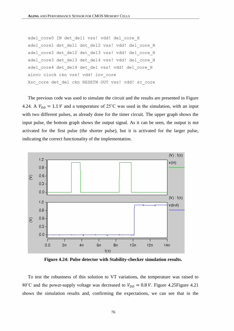
AGING AND PERFORMANCE SENSOR FOR CMOS MEMORY CELLS
76
xdel_core0 IN det_del1 vss! vdd! del_core_H
xdel_core1 det_del1 det_del2 vss! vdd! del_core_H
xdel_core2 det_del2 det_del3 vss! vdd! del_core_H
xdel_core3 det_del3 det_del4 vss! vdd! del_core_H
xdel_core4 det_del4 det_del vss! vdd! del_core_H
xinvc clock ckn vss! vdd! inv_core
Xsc_core det_del ckn RESETN OUT vss! vdd! sc_core
The previous code was used to simulate the circuit and the results are presented in Figure
4.24. A 𝑉𝐷𝐷 = 1.1 𝑉 and a temperature of 25˚C was used in the simulation, with an input
with two different pulses, as already done for the timer circuit. The upper graph shows the
input pulse, the bottom graph shows the output signal. As it can be seen, the output is not
activated for the first pulse (the shorter pulse), but it is activated for the larger pulse,
indicating the correct functionality of the implementation.
Figure 4.24: Pulse detector with Stability-checker simulation results.
To test the robustness of this solution to VT variations, the temperature was raised to
80˚C and the power-supply voltage was decreased to 𝑉𝐷𝐷 = 0.8 𝑉. Figure 4.25Figure 4.21
shows the simulation results and, confirming the expectations, we can see that in the

AGING AND PERFORMANCE SENSOR FOR CMOS MEMORY CELLS
77
presence of VT degradations both pulses are now signalized as errors. This result confirms
the stable and robust behavior of the stability checker in the presence of VT variations.
Figure 4.25: Pulse detector with Stability-checker simulation results with reduced
VDD and increased Temperature.
In a second robustness test, aging degradations were introduced, in the form of 30%
increase in |Vth| values for the transistors. The results are presented in Figure 4.26, and as we
can see, similar results are obtained for VT and Aging degradations (which again confirms
the robustness of the solution for VTA degradations).

AGING AND PERFORMANCE SENSOR FOR CMOS MEMORY CELLS
78
Figure 4.26: Pulse detector with Stability-checker simulation results with |Vth|
increased in 30%.
Considering the complete solution for the sensor, i.e., using the transition detector
(implementation 3) and the pulse detector (stability-checker based implementation),
simulations were performed to validate the entire sensor solution. Now, two different
situations were tested: (1) an input signal with fast up and down transitions (small rise and
fall times), and (2) an input signal with slow up and down transitions (large rise and fall
times). Figure 4.27 shows the results for nominal conditions, Figure 4.28 for sensor’s
operation with VT degradations (T=80˚C, 𝑉𝐷𝐷 = 0.8 𝑉) and Figure 4.29 for operation with
aging degradations (30% increase in |Vth|). In these simulations, the first graph in each
figure shows the input signal, representing the memory bit lines; the second graph shows the
transition detector output signal, showing the pulses generated for each input signal’s
transition; and the third graph in each figure shows the output of the pulse detector (sensor’s
output), indicating with an high state when a performance error has occurred.
As it can be seen, for nominal conditions the error is only signalized for the slower
transition (Figure 4.27). However, when VTA variations occur, both slower and faster
transitions are signalized at the output as errors, due to the performance reduction achieved
with VTA variation (Figure 4.28 and Figure 4.29).

AGING AND PERFORMANCE SENSOR FOR CMOS MEMORY CELLS
79
Figure 4.27: Results for complete sensor simulation (transition detector
implementation 3 + pulse detector with Stability-checker implementation).
Figure 4.28: Sensor simulation results (transition detector implementation 3 + pulse
detector with Stability-checker implementation) in the presence of VT degradations.

AGING AND PERFORMANCE SENSOR FOR CMOS MEMORY CELLS
80
Figure 4.29: Sensor simulation results (transition detector implementation 3 + pulse
detector with Stability-checker implementation) in the presence of Aging degradations.
The previous section presented a robust pulse detector implementation. However, the
obtained circuit can be improved, because the stability checker used has the property to
detect any changes at its input (a rise or fall transition), but its application as a pulse detector
needs to detect if the pulse arrives after a pre-defined instant (defined by the clock).
Therefore, the same functionality can be implemented in an improved version of the pulse
detector, reducing the number of transistors used (and thus reducing the sensor’s size and
area overhead). The next section presents a new and improved pulse detector
implementation.
4.2.3 NOR-BASED PULSE DETECTOR
In order to simplify the stability-checker functionality when applied to a pulse detector, a
new pulse detector implementation was tried, the NOR-based pulse detector presented in this
section. The idea is to use the NOR functionality to detect when simultaneously two signals
are at low state. Considering that signals in the memory are generated in the rise edge of the

AGING AND PERFORMANCE SENSOR FOR CMOS MEMORY CELLS
81
clock, the pulses in the pulse detector’s input will occur also during the high state of the
clock. Hence, considering that a small pulse will be produced for a fresh memory a cell and
that a large pulse will be produced when a PVTA error occurs, the error detection should
occur during the low state of the clock. Using the NOR functionality, the input pulse must be
inverted, i.e., active low. Besides, to allow a better control of the error/non-error pulse
durations, we include a delay element in the input signal to postpone pulse activation.
Therefore, by design we have two parameters to control the activation (and non-activation)
of the sensor: the sensibility of the transition detector (and the number of inverters to use in
the two paths), and the time delay introduced by the delay element.
The NOR-based pulse detector implementation (Figure 4.30), uses 4 transistors to
implement a CMOS NOR logic gate (M1, M2, M4 and M5), controlled by a clock signal
(CLOCK) and delayed pulses (Delayed_Pulse). The inverter and the transistors M3 and M6
ensure, in case of a detection, that the output remains active until a reset occur (this allows to
exempt the use of a latch to keep the sensor active in case of an error). The reset signal
(RESET) controls M7 transistor operation, and reinitiates all the circuit for a new detection.
Figure 4.30: NOR based pulse detector.

AGING AND PERFORMANCE SENSOR FOR CMOS MEMORY CELLS
82
Figure 4.31 shows the control signals for the NOR-based pulse detector functionality.
When the inverted delayed pulse reaches the low state of the clock, an error signal is
signalized at the output.
Figure 4.31: NOR based pulse detector.
The NOR based pulse detector was implemented on SPICE and its netlist is the following
code snippet.
xdel_core0 IN det_del1 vss! vdd! del_core_H
xdel_core1 det_del1 det_del2 vss! vdd! del_core_H
xdel_core2 det_del2 det_del3 vss! vdd! del_core_H
xdel_core3 det_del3 det_del4 vss! vdd! del_core_H
xdel_core4 det_del4 det_del vss! vdd! del_core_H
Xinv66 det_del det_del_neg vss! vdd! INV0
xp0 t1 det_del_neg vdd! vdd! PMOSFET
xp1 out clock t1 vdd! PMOSFET
xn0 out clock t2 vss! NMOSFET
xn1 out det_del_neg t2 vss! NMOSFET
xp2 out t3 vdd! vdd! PMOSFET
xn2 t2 t3 vss! vss! NMOSFET
Xout out t3 vss! vdd! INV0
xn3 out RESET1 vss! vss! NMOSFET W='5*WNmin'

AGING AND PERFORMANCE SENSOR FOR CMOS MEMORY CELLS
83
To test the NOR pulse detector performance, an HSPICE simulation was performed with
temperature of 25 ˚C and 𝑉𝐷𝐷 = 1.1𝑉. Figure 4.32 shows the simulation results when the
pulse detector was stimulated with two different pulses, a short pulse and a large pulse. The
upper graph shows the input pulses, the middle graph shows the inverted delayed pulses and
the clock signals, and the bottom graph shows the output signal. As it can be seen, the output
is only activated for the second and large pulse, showing that the circuit functionality is
correct. It is important to note that the clock signal plays an important role to synchronize the
detection timing.
Figure 4.32: NOR based pulse detector, detections test.
The circuit was then submitted to VT variations, simulating again the pulse detector for
𝑉𝐷𝐷 = 0.8 𝑉 and with a temperature of 80 ˚C. The results are presented in Figure 4.33, and
show the error detection for both of the pulses, due to the increased performance degradation
due to VT variation. This is an important result for the sensor, because it shows that the
sensor is more sensible to performance variations when the environment variables impose

AGING AND PERFORMANCE SENSOR FOR CMOS MEMORY CELLS
84
worst operating conditions. This way, the sensor will work prudently, signalizing faults with
higher sensibility when the environmental conditions increase the error probability.
Figure 4.33: NOR based pulse detector, VT variations test.
In a second robustness test, aging degradations were introduced, in the form of 30%
increase in |Vth| values for the transistors. The results are presented in Figure 4.34 and, as we
can see, similar results are obtained for VT and Aging degradations. These results confirm
the robustness of the solution for VTA degradations.

AGING AND PERFORMANCE SENSOR FOR CMOS MEMORY CELLS
85
Figure 4.34: NOR based pulse detector, Aging variations test.
Considering the complete solution for the sensor, i.e., using the transition detector
(implementation 3) and the pulse detector (NOR-based implementation), simulations were
performed to validate the entire sensor solution. As done in the previous section, two
different situations were tested: (1) an input signal with fast up and down transitions (small
rise and fall times), and (2) an input signal with slow up and down transitions (large rise and
fall times). Figure 4.35 shows the results for nominal conditions, Figure 4.36 for sensor’s
operation with VT degradations (T=80˚C, V_DD=0.8 V) and Figure 4.37 for operation with
aging degradations (30% increase in |Vth|). In these simulations, the first graph in each
figure shows the input signal, representing the memory bit lines; the second graph shows the
transition detector output signal, showing the pulses generated for each input signal’s
transition; the third graph shows the clock signal and the inverted delayed pulse, which must
be both at low state to activate sensor’s output; and the last graph in each figure shows the
output of the pulse detector (sensor’s output), indicating with an high state when a
performance error has occurred.

AGING AND PERFORMANCE SENSOR FOR CMOS MEMORY CELLS
86
Figure 4.35: Sensor simulation results (transition detector implementation 3 + pulse
detector with NOR-based implementation) at nominal conditions.
Figure 4.36: Sensor simulation results (transition detector implementation 3 + pulse
detector with NOR-based implementation) in the presence of VT degradations.

AGING AND PERFORMANCE SENSOR FOR CMOS MEMORY CELLS
87
Figure 4.37: Sensor simulation results (transition detector implementation 3 + pulse
detector with NOR-based implementation) in the presence of Aging degradations.
As it can be seen, for nominal conditions the error is only signalized for the slower
transition (Figure 4.25). However, when VTA variations occur, both slower and faster
transitions are signalized at the output as errors, due to the performance reduction achieved
with VTA variation (Figure 4.26 and Figure 4.27).
4.3 COMPLETE SENSOR WITH AN SRAM CELL
The previous sections allowed us to define the robust implementations for the sensor.
From section 4.1, the best implementation for the transition detector was define, the
implementation 3. From section 4.2, the optimize solution for the pulse detector was
obtained for the NOR-based implementation. Therefore, the complete and final architecture
for the performance and aging sensor for memory circuits is presented in Figure 4.38.
Nevertheless, there are two variables that should be adjusted and validated when connecting

AGING AND PERFORMANCE SENSOR FOR CMOS MEMORY CELLS
88
the sensor to a memory circuit: (1) the number of inverters in the two paths of the transition
detector, and consequently their delay; and (2) the number of buffer elements used in the
delay element of the pulse detector, and consequently its delay. These two parameters
depend on the clock frequency used, on sensor’s sensibility needed to detect a performance
degradation, on the CMOS technology used. The sensor’s sensibility needed can vary with
the memory size and capacity, which affects the parasitic capacitance in the bit-lines, and
also with the type of memory used (SRAM or DRAM), because the pre-charge values for the
bit-lines may differ (usually the bit-lines in SRAMs are pre-charged at VDD, and in DRAMs
are pre-charged at VDD/2) and sensor’s sensibility must be defined accordingly.
Figure 4.38: Aging and performance sensor schematic.
To complete the sensor design, it is important to test sensor’s behavior in a complete
memory circuit, in order to apply the correct stimuli to the sensor and to test it in a real
situation. Therefore, the sensor was deployed and connected to the bit line of an SRAM cell.
Moreover, as the recent nanotechnologies available commercially use smaller CMOS
technologies, it is important to evaluate sensor’s behavior at newer transistor’s sizes. As a
consequence, the sensor and the SRAM memory cell was implemented in a 22nm CMOS
technology, using Berkeley’s Predictive Technology Models to simulate the behavior in
HSPICE.
It is important to note that aging degradations in 65nm are mostly induced by NBTI
effect. However, from 32nm and below, other materials are used along with silicon, and also
different structures for the transistors, to reduced channel’s leakage and also improve
transistor’s performance at reduced sizes. Some examples are the High-K metal gate
transistors, or the newer 23nm FINFET transistors and their 3D structures. At these reduced
sizes, both NBTI and PBTI are important effects, and their impact on performance is similar.
Therefore, it is also very important to test the sensor in two different technologies.

AGING AND PERFORMANCE SENSOR FOR CMOS MEMORY CELLS
89
The following test was carried out in a 22nm CMOS technology, using a one SRAM cell,
along with the sense amplifier and the remaining circuitry, and a sensor connected to the
cell’s bit line, to actively monitor the transitions and detect aging on the memory cell. The
simulating conditions were 𝑉𝐷𝐷 = 0.95𝑉, with temperature at 25 ˚C (nominal conditions),
and to simulate a fresh SRAM cell, the Vth nominal values of PTM 22nm transistors’
models were used: 𝑉𝑡ℎ_𝑝 = −0.63745 V and 𝑉𝑡ℎ_𝑛 = 0.68858 V.
Figure 4.39 presents the simulation results for read and write operations: the bottom graph
shows the bit line signal (bl) and the complementary bit line (blb) (the blue and green
signals, respectively); the middle graph shows the clock signal and the inverted pulses
obtained from each bit-line transition (light green and red signals, respectively); and the
upper graph shows the sensor output signal. As can be observed, no error was signalized at
the output, because the inverted pulses occurred during the high pulse of the clock.
Figure 4.39: Aging and performance sensor with a fresh SRAM cell.
To test a detection the SRAM cell was aged and a |Vth| increase of 10% was applied to
the transistors, simulating the NBTI and PBTI effects which degrade the transistors
performance (the values used were: 𝑉𝑡ℎ_𝑝 = −0.701195 and 𝑉𝑡ℎ_𝑛 = 0.757438). In Figure
4.40 the simulation result is observed. The first inverted pulse (red color) increased its pulse
width, due to slower transition on the bit-line, activated by aging. As a result, the rising edge
of the pulse overlaps the detection window (the low state of the clock) and the aging and
performance sensor outputs a ‘1’, signalizing an error (grey color).

AGING AND PERFORMANCE SENSOR FOR CMOS MEMORY CELLS
90
Figure 4.40: Aging and performance sensor detection with SRAM 10% aged.

91
5. IMPLEMENTATION AND RESULTS
In this chapter, the complete layout implementations for the sensor and for an SRAM are
presented, along with the spice simulation results for the extracted netlist (netlist extracted
from the layout, with all the parasitic capacitances present). It is important to note that the
developed sensor can be applied on SRAMs or DRAMs, because it is connected to the
bitlines and its behavior is independent on the memory structure. However, for
demonstration purposes, in this work only SRAM circuits were used to drive and
demonstrate the sensor, leaving the DRAM sensor tests for future work.
The layouts were designed using the Microwind software tool from [37], using CMOS
22nm foundry available with the software tool.
5.1 LAYOUT 1 BIT SRAM
As explained in the previous section, the sensor complete design should be defined
according with the memory circuit where it will be placed. So, let us first design a 1 bit
SRAM cell and the remaining memory circuitry (sense amplifier, pre-charge and equalizer
and read/write circuitry).
5.1.1 SRAM CELL
Figure 5.1 presents the layout of the SRAM cell. The two inverters are composed by the
PMOS transistor with W=70 nm, the NMOS transistor with W=40 nm, and the channel
length is L=20 nm for all the transistors. The NMOS access transistors, activated by the

IMPLEMENTATION AND RESULTS
92
word line (WL) are designed with W=90 nm to provide an extra drive capability and allow
cell’s writing.
The SRAM cell characteristics are:
- Width: 0.5µm (46 lambda);
- Height: 0.6µm (62 lambda);
- Surface area: 0.3µm2.
Figure 5.1: SRAM cell layout.
5.1.2 SENSE AMPLIFIER
The sense amplifier (Figure 5.2), provides amplification of small signal differences
between the bit lines, responding with a full swing signal to guarantee the usage of the

IMPLEMENTATION AND RESULTS
93
correct logic levels. The sense amplifier is controlled by the sense signal (Φ𝑠). As it can be
seen in Figure 5.2, the sense signal is connected to an inverter, to generate its complementary
signal (Φ𝑠̅̅ ̅̅ ). This allows to control the sense amplifier circuit, two complementary switches
(transistors) to power-up the sense amplifier only when amplification is needed. The PMOS
transistors are designed with the minimum sizes (W=70 nm). The inverter NMOS is W=40
nm, the cross-coupled NMOS inverters are W=50 nm and the control NMOS is designed
with 60 nm.
The sense amplifier characteristics are:
- Width: 0.6µm (60 lambda);
- Height: 0.7µm (65 lambda);
- Surface area: 0.4µm2.
Figure 5.2: Sense amplifier layout.

IMPLEMENTATION AND RESULTS
94
5.1.3 PRE-CHARGE AND EQUALIZER
In Figure 5.3 can be observed the pre-charge and equalizer circuitry, controlled by the
signal Φ𝑃. This circuit pre-charges and equalizes both bit lines to 𝑉𝐷𝐷, before a cell
read/write. The size of the PMOS transistors is W= 70 nm.
Figure 5.3: Pre-charge and equalizer layout.
The precharge and equalizer characteristics are:
- Width: 0.3µm (29 lambda);

IMPLEMENTATION AND RESULTS
95
- Height: 0.7µm (65 lambda);
- Surface area: 0.2µm2.
5.1.4 WRITE CIRCUITRY
The write circuitry presented in Figure 5.4, forces the bit line with the logic values
intended to write on the SRAM cell (logic ‘0’ or ‘1’). On the “write data” signal are placed
the bits to send to the SRAM cell, while the “write enable” activates the NMOS transistors
(W=90nm) that send the values to the bit lines. The inverters are designed with NMOS
W=50nm and PMOS W=80 nm.
Figure 5.4: Write circuit layout.
The write circuitry characteristics are:

IMPLEMENTATION AND RESULTS
96
- Width: 0.5µm (52 lambda);
- Height: 0.7µm (66 lambda);
- Surface area: 0.3µm2.
5.1.5 COMPLETE SRAM CELL
The SRAM cell was connected to all its remaining circuitry and the complete 1 bit SRAM
cell is presented in Figure 5.5.
Figure 5.5: Complete 1 bit SRAM cell.
The complete SRAM cell characteristics are:
- Width: 1.7µm (170 lambda);
- Height: 0.6µm (62 lambda);
- Surface area: 1.1µm2.
The complete SRAM cell was simulated with the Microwind simulator, to validate the
layout. In this test, the following operations were considered: write ‘1’, read ‘1’, write ‘0’
and read ‘0’.
Figure 5.6 presents the results of simulation, for write and read operation. The top 5
signals represent the control signals, namely: pre-charge (Φ𝑃), sense amplifier (Φ𝑠), word
line (wl), write data and enable data. The control signals are disposed in order to perform the
operations as described in detail in section 3.5. The Q signal shows the memory content, and

IMPLEMENTATION AND RESULTS
97
a ‘1’ is stored during the first write and read operations, and a ‘0’ is stored for the second
write and read operations. The bit line (BL) is initialized at 𝑉𝐷𝐷, due to the pre-charge and
equalizer circuit. After the first initialization, it continues at this value because the writing
circuit is forcing a ‘1’ on the bit line. Approximately in the middle of the simulation (at 14
ns), the bit line drops to ‘0’, due to the write of a ‘0’.
Figure 5.6: SRAM read and write cycle.
5.2 AGING AND PERFORMANCE SENSOR LAYOUT
This section presents the layouts for the complete Aging and Performance sensor.

IMPLEMENTATION AND RESULTS
98
5.2.1 TRANSITION DETECTOR’S DATA PATHS
Figure 5.7 shows the layout of the transition detector. The transition detector is built by
two paths with 4 inverters each, alternating in a more conductive PMOS or NMOS
MOSFET, in a total of 8 inverters.
Figure 5.7: Transition detector layout.
The minimum size for the PMOS transistor is W=50nm and for the NMOS is W=40nm.
The design of the more conductive transistors was done using a 3 finger gate to occupy the
space more efficiently on the cell; the NMOS size is W=80nm and the PMOS is also W=80
nm.
The characteristics of the transition detector are:
- Width: 1.9µm (194 lambda);
- Height: 0.7µm (67 lambda);
- Surface area: 1.3µm2.
5.2.2 XOR WITH TRANSMISSION GATES
The XOR with transmission gate and pass-transistor logic (Figure 5.8) is built with the
minimum transistor sizes PMOS W=70nm and NMOS W=40nm. The XOR with
transmission gate integrates the transition detector block, being responsible to generate pulse
as a transition occurs. The transmission gate ensures an output without logic levels
degradation.

IMPLEMENTATION AND RESULTS
99
Figure 5.8: XOR with transmission gate.
The characteristics of the XOR with transmission gates are:
- Width: 0.9µm (89 lambda);
- Height: 0.6µm (59 lambda);
- Surface area: 0.5µm2.
5.2.3 DELAY ELEMENT
The delay element (DE_H) provides a time delay, to generated pulses from the transition
detector (Figure 5.9). The delayed pulses are then inverted (Inv_Del_Pulses) to be used on
the detection window. The sizes of the transistors are PMOS W=70nm and NMOS
W=40nm.
The delay element characteristics are:
- Width: 0.7µm (69 lambda);
- Height: 0.6µm (59 lambda);
- Surface area: 0.4µm2.

IMPLEMENTATION AND RESULTS
100
Figure 5.9: Delay element (DE_H).
5.2.4 NOR BASED PULSE DETECTOR
The NOR based pulse detector (Figure 5.10) is controlled by the clock signal (CLK), the
reset signal and also receives the delayed inverted pulses. This circuit outputs ‘1’, when the
clock signal and the inverted pulses are both ‘0’, following the detection window. All the
transistors use the minimum sizes PMOS W=70nm, NMOS W=40nm and the reset NMOS
uses W=60nm for extra drive capability.
The NOR characteristics are:
- Width: 0.6µm (60 lambda);
- Height: 0.7µm (66 lambda);
- Surface area: 0.4µm2.

IMPLEMENTATION AND RESULTS
101
Figure 5.10: NOR based pulse detector.
5.2.5 COMPLETE AGING AND PERFORMANCE SENSOR
Figure 5.11 shows the complete aging and performance sensor. The design characteristics
are:
- Width: 3.9µm (389 lambda);
- Height: 0.7µm (69 lambda);
- Surface area: 2.7µm2.
Figure 5.11: Complete aging and performance sensor.

IMPLEMENTATION AND RESULTS
102
To test the complete aging and performance sensor, it was place at the input a square
pulse with 1 ns of duration. From Figure 5.12 we can see the generation off two inverted
pulses due to the rise/fall transitions at the input. The output is activated and, consequently,
an error is signalized. Please note that this simulation was performed with Microwind
simulation tool.
Figure 5.12: Aging and performance sensor simulation.
5.3 RESULTS FOR SRAM WITH AGING AND PERFORMANCE SENSOR
In this section, layouts are presented with both the SRAM and the sensor. Also,
simulations were performed for the complete circuit and the results are here presented.

IMPLEMENTATION AND RESULTS
103
5.3.1 1 BIT SRAM IMPLEMENTATION
The layout of the aging and performance sensor was deployed on a 1 bit SRAM cell,
complete and including its peripherals (Figure 5.13).
The implementation characteristics are:
- Width: 5.5µm (548 lambda);
- Height: 0.7µm (72 lambda);
- Surf: 3.9µm2.
Figure 5.13: Aging and performance sensor 1 bit SRAM implementation.
The netlist was extracted from the layout design on Microwind and then simulated on
HSPICE. Figure 5.14 shows a situation of no detection. The inverted pulses generated (blue
color) are contained inside of the clock pulse (which is not seen in this figure), thus not
entering on the detection window, meaning the presence of a fresh memory cell.
Figure 5.14: Aging sensor deployed on a fresh 1bit SRAM cell.
The SRAM cell was aged, by changing the Vth nominal values in 10%, for PTM 22nm
transistor model: 𝑉𝑡ℎ_𝑝 = −0.63745 and 𝑉𝑡ℎ_𝑛 = 0.68858.

IMPLEMENTATION AND RESULTS
104
In Figure 5.15, it can be observed that the aging degradations of 10% increase in |Vth|
cause the increase of pulse width and also shifts the position of the inverted pulses, due to
the decrease of performance caused by the transistors aging. This way the pulses enter the
detection window, and the sensor responds ‘1’ to the output, which means an error caused by
circuits’ aging.
Figure 5.15: Aging sensor deployed on a 10% aged 1bit SRAM cell.
5.3.2 8 BIT SRAM IMPLEMENTATION
Figure 5.16 shows the implementation of the aging and performance sensor on an 8 bit
SRAM memory array.
The implementation characteristics are:
- Width: 8.3µm (829 lambda);
- Height: 0.7µm (72 lambda);
- Surface area: 6.0µm2.
Figure 5.16: Aging and performance sensor 8 bit SRAM implementation.

IMPLEMENTATION AND RESULTS
105
The netlist was extracted from the layout design on Microwind and then simulated on
HSPICE. To give an easier perception two simulations were performed, one focusing on the
8 bit SRAM operation and another using the 8 bit SRAM and the aging sensor.
To test the 8 bit SRAM array it was written an 8 bit word (10001111) inside the SRAM
memory, following the read operation, seen in Figure 5.17.
Figure 5.17: Write and read on an 8bit SRAM array.
The top signal seen in the figure represents the write enable, activating the write circuit.
The pink signal below is the write data and has the 8 bit information to write inside the
SRAM. Each memory cell is controlled by a Word Line (WL) signal. This array is built with
8 memory cells, thus 8 WL signals are used. However to show a more readable figure only 3
WL signals are seen: WL0, WL1 and WL2.
The 𝐵𝐿 and 𝐵𝐿̅̅̅̅ signals, validate the correct operation of the 8 bit SRAM array.
In Figure 5.18 it is observed a test on the aging and performance sensor, on the 8 bit
SRAM array. The inverted pulses generated by the bit line, occurred during the active pulse
of the clock, not entering this way on the detection window, and the error is not signalized.

IMPLEMENTATION AND RESULTS
106
Figure 5.18: Aging and performance sensor on an 8bit SRAM array.
In Figure 5.19 it can be observed an error detection, occurred on a simulation with aging
of 10% increase in |Vth|. The aging on SRAM transitions cause the increase of the pulse
width, observed in the inverted pulses, and also a small pulse shift, entering on the detection
window and signalizing an error to the output.
Figure 5.19: Aging and performance sensor on an 8bit SRAM array aged 10%.

IMPLEMENTATION AND RESULTS
107
5.3.3 64 BIT SRAM IMPLEMENTATION
Figure 5.20 shows a 64 (8x8) bit SRAM implementation, 8 rows and 8 columns. The
implementation characteristics are:
- Width: 8.5µm (851 lambda);
- Height: 4.3µm (434 lambda);
- Surface area: 36.9µm2.
Figure 5.20: Aging and performance sensor 64 bit SRAM implementation.
Each bit line column uses an aging and performance sensor, analyzed previously, to
monitor each column of 8 bit SRAM cell. Since the working principle is the same, in this
section is only shown an implementation for 64 bit.

IMPLEMENTATION AND RESULTS
108

109
6. CONCLUSIONS AND FUTURE WORK
6.1 CONCLUSIONS
This thesis focused on the development of an aging and performance sensor for CMOS
memories, detecting and signalizing the aging and performance degradation on SRAM
memory cells.
The downsizing of new technologies leads to an exponential raise on variability and IC
sensitivity to disturbances, externals and internals. The continuous evolution to a smaller
scale devices, makes the variability a major concern, affecting the digital circuit’s
performance, and its reliable operation. The circuits aging over the time, reflects longer
propagation delays and slower signal transitions, and degrades the circuit’s performance.
From all aging effects the BTI (Bias Thermal Instability) is pointed as the most relevant
effect for the performance loss. The NBTI (Negative BTI) effect, affects technologies bellow
130nm, using SiO2 dielectric with polysilicon gate devices, affecting mainly the PMOS
MOSFETS. The PBTI (Positive BTI) effects affects the NMOS transistors, and for
technologies bellow 32nm and using high-k metal gates, the degradations are similar to
NBTI. The degradation caused by PBTI and NBTI on the transistors, manifests itself through
the increase of |𝑉𝑡ℎ| over the time. Process, power supply Voltage, Temperature and Aging
(PVTA), are four parameters that can influence enormously the performance of nanometer
technologies. High operation temperatures, are responsible for the increase of circuits aging,
and lower power-supply voltages slows down the circuit’s performance, due to switching
activity.
Several aging sensor solutions were already proposed in the literature and studied in this
work, namely the On-Chip Aging Sensor [9] and the Scout Flip-Flop [11]. However, these
solutions have several disadvantages, as it was highlighted in this thesis, and the search for a

CONCLUSIONS AND FUTURE WORK
110
better aging and performance sensor for CMOS memories was the purpose of the research
developed in this thesis.
In this work, the attention was focused on CMOS memory cells’ aging, and how its
performance degradation affects the basic memory cell operations, the read the write and
also the data hold. The main goal was to develop a new aging and performance sensor,
aiming the identification and signalization of slow transitions occurrences on memory cells
caused by the aging. The aging and performance sensor is connected to the bit-lines and
actively monitors the transition delays of the read and write transitions. The sensor has a
detection window defined by the clock signal (the inactive fraction of the clock), and when
the aging occurs, degrading the MOSFETS properties (in specific the increase of |𝑉𝑡ℎ|), it
will cause a slower transistor switching, which will be signalized as an error (logic ‘1’) by
the sensor output.
Regarding the applicability of the sensor to DRAMs, it is important to note that it can be
used both in SRAM or DRAM cells because the sensor is connected to the bit-lines (which
are present in both types of memories), monitoring their transitions. However, in this work
the sensor was tested only in SRAM cells. Some memory architectures (like DRAMs) may
impose additional problems when bit-lines are pre-charged at VDD/2 values, creating smaller
and fast transitions in the bit-lines. Moreover, the additional problem in DRAMs is that the
critical operation of a memory cell is when the charge is not sufficient to drive an inequality
in the bit-lines and allow the sense amplifier to detect the saved bit. I.e., the problem in
DRAMs is not usually the transition timings but rather the reliable identification of the logic
level and the data hold.
From the sensor development, we can conclude that it is not easy to create and develop a
robust design, because of the several constraints present: sensitive to voltage, temperature,
aging, with reduced surface area, imposing no impact on memory’s performance degradation
(due to the additional capacitance), etc.
In respect to VTA degradations, it was only possible to develop a solution that increases
sensibility when increasing degradations are present when a fixed clock signal is used, to
create a fixed detectability window. Although the clock signal is not present if we consider
the basic cell circuitry, when considering the accessibility circuitry and signals (decoders,
multiplexers) and the read and write signals’ generation, a clock signal is normally present,
so this is not a problem.

CONCLUSIONS AND FUTURE WORK
111
Regarding the additional capacitance connected to the memory, by installing the sensor,
no test was performed to measure memory’s performance degradation. However, we believe
that the impact of the sensor in the cell performance is completely negligible, because bit-
lines have high parasitic capacitances, due to the high number of cells connected, and the
sensor connection uses a small delay element (which is a simple buffer) to connect to the bit-
lines. Therefore, the degradation is similar to an additional memory bit, which is negligible if
we consider a high capacity memory.
From sensor development we can also conclude that two possible implementations for a
robust sensor were obtain. Regarding the transition detector, one robust implementation was
achieved, implementation 3, which uses a pass-transistor logic XOR gate. Regarding the
pulse detector, two robust possible implementations were achieved: the stability-checker
based and the NOR-based pulse detector. From our analysis, the NOR-based implementation
is preferred because it’s a simpler circuit and with less area overhead.
The extensive SPICE simulations at the transistor level, for both pre-layout and post-
layout simulations, showed that is possible do detect slow transitions at the bit-lines, which
occur from read and write operations to the memory. Moreover, the sensor was tested with
VT degradations and with aging degradations, and the results indicate that the sensor is
robust, being more sensible when these degradations occur. This result is very important,
because it brings additional improvements to memory sensors, namely its adaptive
sensibility to PVTA variations, and changes the paradigm of memory sensors. In the
presence of enhanced variability in PVTA degradations, the sensor increases its sensitivity to
detect slower performances in memory circuits’ operation, by increasing locally the pulse
duration in the pulse detector, and by increasing the delays in the transition detector,
according with the local PVTA variations. This feature simplifies also sensor design, as the
sensor itself does not need to be more robust to PVTA variations than the circuit where it is
installed. On the contrary, sensor’s performance degradation due to PVTA improve its
sensibility to detect slower transitions in the bit-lines. Thus, sensor aging works in favor of
its sensibility. In fact, to avoid errors, when PVTA variations increase, we have to be more
cautious on avoiding errors, and it’s a good principle that sensor’s sensibility should
increase.
An additional good result from the developed sensor is that it can be always active,
monitoring every transition that occurs in the memory. However, considering that transistors
age more when they are statically in stress mode, it can be a problem if a transistor is in

CONCLUSIONS AND FUTURE WORK
112
stress mode for a long time, having no other activity and having a considerable aging
degradation, and sensor cannot detect the aging degradation because there is no activity.
Therefore, it is recommended that, sparsely in time, at least a memory read operation should
be executed, to stimulate sensor operation.
6.2 FUTURE WORK
Every research work is an unfinished task and many future perspectives are now open for
this work.
A first future work is, as previously mention, to study and test sensor’s applicability to
DRAMs, with all of the particularities that DRAM’s operation have.
A second and important future work consists in the usage of the aging and performance
sensor to control the memories cell voltage and frequency operation, ensuring an
optimization point where the voltage and frequency are the minimal as possible, and that
SNM is the limit value to guarantee the cells robustness of operation. This way the cell will
operate with the minimum required power and, due to the SNM monitoring, basic cells’
operations will be guaranteed, in particular the read and write operations and also the data
contents retention. Considering that power reduction schemes and power reduction
methodologies are being widely used in digital integrated circuits, the existence of a
methodology to control power and performance in memories is a need for current circuits
and applications. Moreover, sub-threshold operation of the sensor should also be validated,
to allow more aggressive low-power techniques.
A third future work consists in the application and characterization of the aging and
performance sensor, to a multiple memory cell structure, in order to increase the sensors test
scope, and prepare it to real silicon implementation.
Finally, a fourth task for future work is to implement the aging and performance sensor,
on a real silicon test chip, particularly on a CMOS SRAM memory, to validate the proposed
sensor in a real silicon prototype.

113
REFERENCES
[1] C. Mack, “Fifty Years of Moore’s Law,” in IEEE Transactions on Semiconductor
Manufacturing, vol. 24, no. 2, pp. 202–207, October 20, 2011,
DOI:http://dx.doi.org/10.1109/TSM.2010.2096437.
[2] “IBM Research Alliance Produces Industry’s First 7nm Node Test Chips", in IBM
News Releases, July 2015, [Online]. Available: http://www-
03.ibm.com/press/us/en/pressrelease/47301.wss. [Accessed: 9 July, 2015].
[3] J. Semião, M. Irago, J. Rodríguez-Andina, L. Piccoli, F. Vargas, M. Santos, I.
Teixeira, and J. Teixeira, “Signal Integrity Enhancement in Digital Circuits,” in IEEE
Design and Test of Computers, vol. 25, no. 5 pp. 452–461, September-October, 2008,
DOI:http://dx.doi.org/10.1109/MDT.2008.146.
[4] W. Wang, S. Yang, S. Bhardwaj, R. Vattikonda, S. Vrudhula, F. Liu, and Y. Cao,
“The Impact of NBTI on the Performance of Combinational and Sequential Circuits,”
in Design Automation Conference, pp. 364–369, San Diego, CA, USA, 4-8 June,
2007, DOI:http://dx.doi.org/10.1109/DAC.2007.375188.
[5] T. Kim and Z. Kong, “Impact Analysis of NBTI/PBTI on SRAM VMIN and Design
Techniques for Improved SRAM VMIN”, in Journal of Semiconductor Technology and
Science., vol. 13, no. 2, pp. 87–97, April, 2013,
DOI:http://dx.doi.org/10.5573/JSTS.2013.13.2.87.
[6] “Design for Variability: Managing Design, Process, and Manufacturing Variations in
Physical Design”, Mentor Graphics, 2008 [Online]. Available:
http://s3.mentor.com/public_documents/whitepaper/resources/mentorpaper_43548.pdf
. [Accessed: 19 Aug 2015].
[7] J. McPherson, “Reliability Challenges for 45nm and Beyond,” in Design Automation
Conference, 2006 43rd ACM/IEEE, pp. 176–181, San Francisco, CA, USA, 2006,
DOI:http://dx.doi.org/10.1109/DAC.2006.229181.
[8] B. Paul, K. Kang, H. Kufluoglu, M. Alam, and K. Roy, “Temporal Performance
Degradation under NBTI: Estimation and Design for Improved Reliability of
Nanoscale Circuits,” in Proceedings of the Design Automation and Test in Europe
Conference, vol. 1, pp. 1-6, Munich, Germany, 6-10 March, 2006,
DOI:http://dx.doi.org/10.1109/DATE.2006.244119.
[9] A. Ceratti, T. Copetti, L. Bolzani, and F. Vargas, “On-Chip Aging Sensor to Monitor
NBTI Effect in Nano-Scale SRAM,” in Proceedings of the 2012 IEEE 15th

REFERENCES
114
International Symposium on Design and Diagnostics of Electronic Circuits and
Systems, DDECS 2012, pp. 354–359, Tallinn, Estonia, 18-20 April, 2012,
DOI:http://dx.doi.org/10.1109/DDECS.2012.6219087.
[10] J. Semião, R. Cabral, C. Leong, M. Santos, I. Teixeira, J. Teixeira,, “Dynamic Voltage
Scaling with Fault-Tolerance for Lifetime Operation”, in The Fourth Workshop on
Manufacturable and Dependable Multicore Architectures at Nanoscale (MEDIAN'15)
/ DATE’2015 Workshop W06, Grenoble, France, 13 March, 2015
[11] J. Semiao, A. Romao, D. Saraiva, C. Leong, M. Santos, I. Teixeira, and P. Teixeira,
“Performance Sensor for Tolerance and Predictive Detection of Delay-Faults”,
accepted for publication in the DFT (International Symposium on Defect and Fault
Tolerance in VLSI and Nanotechnology Systems) Symposium 2014, 2014, Amsterdam,
The Netherlands, October 1-3, 2014,
DOI:http://dx.doi.org/10.1109/DFT.2014.6962092.
[12] S. Kumar, C. Kim, and S. Sapatnekar, “Adaptive Techniques for Overcoming
Performance Degradation Due to Aging in CMOS Circuits,” in IEEE Transactions on
Very Large Scale Integration (VLSI) Systems, vol. 19, no. 4, pp. 603–614, April,
2011, DOI:http://dx.doi.org/10.1109/TVLSI.2009.2036628.
[13] A. Calimera, E. Macii, and M. Poncino, “Analysis of NBTI-Induced SNM
Degradation in Power-Gated SRAM Cells,” in IEEE International Symposium on
Circuits and Systems - ISCAS, pp. 785–788, Paris, France, 30 May - 2 June, 2010
DOI:http://dx.doi.org/10.1109/ISCAS.2010.5537452.
[14] A. Islam, H. Kufluoglu, D. Varghese, S. Mahapatra, and M. Alam, “Recent Issues in
Negative-Bias Temperature Instability: Initial Degradation, Field Dependence of
Interface Trap Generation, Hole Trapping Effects, and Relaxation,” in IEEE
Transactions on Electron Devices, vol. 54, no. 9, pp. 2143–2154, September, 2007,
DOI:http://dx.doi.org/10.1109/TED.2007.902883.
[15] C. Martins, J. Semião, J. Vazquez, V. Champac, M. Santos, I. Teixeira, and P.
Teixeira, “Adaptive Error-Prediction Flip-flop for Performance Failure Prediction
with Aging Sensors,” in IEEE 29th VLSI Test Symposium(VTS), pp. 203–208, Dana
Point, CA, USA, 1-5 May, 2011, DOI:http://dx.doi.org/10.1109/VTS.2011.5783784.
[16] R. Vattikonda, W. Wang, and Y. Cao, “Modeling and Minimization of PMOS NBTI
Effect for Robust Nanometer Design”, in 43rd ACM/IEEE Design Automation
Conference, pp. 1047-1052, San Francisco, CA, USA, 2006,
DOI:http://dx.doi.org/10.1109/DAC.2006.229436.
[17] K. Kang, S. Gangwal, S. Park, and K. Roy, “NBTI Induced Performance Degradation
in Logic and Memory Circuits: How Effectively Can We Approach a Reliability
Solution?”, in Asia South Pacific Design Automation Conference ASP-DAC 2008, pp.
726–731, Seoul, South Korea, 21-24 March, 2008,
DOI:http://dx.doi.org/10.1109/ASPDAC.2008.4484047.
[18] S. Kumar, C. Kim, and S. Sapatnekar, “Impact of NBTI on SRAM Read Stability and
Design for Reliability”, in ISQED 06 Proceeding of the 7th International Symposium

REFERENCES
115
on Quality Electronic Design, pp. 210–218, Washington, DC, USA, 2006,
DOI:http://dx.doi.org/10.1109/ISQED.2006.73.
[19] M. Agarwal, B. Paul, M Zhang, S. Mitra, “Circuit Failure Prediction and Its
Application to Transistor Aging,” 25th IEEE VLSI Test Symposium, pp. 277 – 286,
Berkeley, CA, USA, 6-10 May, 2007, DOI:http://dx.doi.org/10.1109/VTS.2007.22.
[20] S. Drapatz, G. Georgakos, and D. Schmitt-Landsiedel, “Impact of Negative and
Positive Bias Temperature Stress on 6T-SRAM Cells”, in Advances in Radio Science,
vol. 7, pp. 191–196, 19 May, 2009, DOI:http://dx.doi.org/10.5194/ars-7-191-2009.
[21] D. Ioannou, S. Mittl, and G. Rosa, “Positive Bias Temperature Instability Effects in
nMOSFETs With HfO2/TiN Gate Stacks”, in IEEE Transactions on Device Materials
Reliability, vol. 9, no. 2, pp. 128–134, 5 May, 2009,
DOI:http://dx.doi.org/10.1109/TDMR.2009.2020432.
[22] C. Martins, “Adaptive Error-Prediction Aging Sensor for Synchronous Digital
Circuits”, Masters Dissertation, University of Algarve, Faro, Portugal, 2012.
[23] A. Sedra and K. Smith, Microelectronic Circuits, 5th edition, Oxford University
Press, Inc. New York, USA, 2004, pp. 1028–1045.
[24] S. Khasanvis, K. Habib, M. Rahman, P. Narayanan, R. Lake, and C. Moritz, “Ternary
Volatile Random Access Memory based on Heterogeneous Graphene-CMOS Fabric”,
in 2012 IEEE/ACM International Symposium Nanoscale Architectures(NANOARCH),
pp. 69–76, Amsterdam, The Netherlands, 4-6 July, 2012, ISBN: 978-1-4503-1671-2.
[25] Q. Wu and T. Zhang, “Design Techniques to Facilitate Processor Power Delivery in
3-D Processor-DRAM Integrated Systems”, in IEEE Transactions on Very Large
Scale Integration (VLSI) Systems, vol. 19, no. 9, pp. 1655–1666, 19 July, 2010,
DOI:http://dx.doi.org/10.1109/TVLSI.2010.2053565.
[26] S. Pal and A. Islam, “Device Bias Technique to Improve Design Metrics of 6T SRAM
Cell for Subthreshold Operation”, in 2015 2nd International Conference on Signal
Processing and Integrated Networks (SPIN) pp. 865–870, Noida, India 19-20
February, 2015, DOI:http://dx.doi.org/10.1109/SPIN.2015.7095170.
[27] B. Mohammad, P. Dadabhoy, K. Lin, and P. Bassett, “Comparative Study of Current
Mode and Voltage Mode Sense Amplifier Used for 28nm SRAM”, in 2012 24th
International Conference on Microelectronics (ICM), pp. 1-6, Algiers, Algeria, 16-20
December, 2012, DOI:http://dx.doi.org/10.1109/ICM.2012.6471396.
[28] H. Noguchi, Y. Iguchi, H. Fujiwara, Y. Morita, K. Nii, H. Kawaguchi, and M.
Yoshimoto, “A 10T Non-Precharge Two-Port SRAM for 74% Power Reduction in
Video Processing”, in IEEE Computer Society Annual Symposium on VLSI 2007
ISVLSI, pp. 107–112, Porto Alegre, Brazil, 9-11 March 2007,
DOI:http://dx.doi.org/10.1109/ISVLSI.2007.2.
[29] E. Grossar, M. Stucchi, K. Maex, and W. Dehaene, “Read Stability and Write-Ability
Analysis of SRAM Cells for Nanometer Technologies”, in IEEE Journal of Solid-

REFERENCES
116
State Circuits, vol. 41, no. 11, pp. 2577–2588, November, 2006,
DOI:http://dx.doi.org/10.1109/JSSC.2006.883344.
[30] E. Seevinck, F. List, and J. Lohstroh, “Static-Noise Margin Analysis of MOS SRAM
Cells”, in IEEE Journal Solid-State Circuits, vol. 22, no. 5, pp. 748–754, Octorber,
1987, DOI:http://dx.doi.org/10.1109/JSSC.1987.1052809.
[31] E. Vatajelu and J. Figueras, “The Impact of Supply Voltage Reduction on The Static
Noise Margins of a 6T-Sram Cell”, in CEAI, vol. 10, no. 4, pp. 49–54, 2008.
[32] R. Keerthi and C. Chen, “Stability and Static Noise Margin Analysis of Low-Power
SRAM”, in IEEE Instrumentation and Measurement Technology Conference, pp.
1681–1684, Victoria, BC, Canada, 12-15 May, 2008,
DOI:http://dx.doi.org/10.1109/IMTC.2008.4547314.
[33] C. Arandilla, A. Alvarez, and C. Roque, “Static Noise Margin of 6T SRAM Cell in
90-nm CMOS”, in 2011 UKSim 13th International Conference on Computer
Modelling and Simulation, pp. 534–539, Cambridge, England, March 30-1 April,
2011, DOI:http://dx.doi.org/10.1109/UKSIM.2011.108.
[34] N. Rahman and B. Singh, “Static-Noise-Margin Analysis of Conventional 6T SRAM
Cell at 45nm Technology”, in International Journal of Computer Applications (0975-
8887), vol. 66, no. 20, pp. 19–23, March, 2013, DOI:http://dx.doi.org/10.5120/11200-
6274.
[35] J. Pachito, “Metodologia Para Prever o Envelhecimento de Circuitos Digitais”,
Masters Dissertation, University of Algarve, Faro, Portugal, 2012.
[36] J. Semião, H. Santos, A. Romão, "Performance and Aging Sensor for SRAM and
DRAM Memories", Portuguese Patent Pending n. 108852 C, 29 August, 2015.
[37] Microwind Software Tool, [Online]. Available: http://www.microwind.net/.
[Accessed: 9 July, 2015].

APPENDIX
117
7. APPENDIX
A1. Article for Patent Submission
Performance and Aging Sensor for
SRAM and DRAM Memories
J. Semião, H. Santos, A. Romão
ISE – University of Algarve,
Faro, Portugal
{jsemiao, }@ualg.pt
Abstract— CMOS memories occupy a significant
percentage of the Integrated Circuits footprint. With
the development of new manufacturing technologies to
a smaller scale, issues about performance and
reliability exist. Effects such as BTI (Bias Thermal
Instability), TDDB (Time Dependent Dielectric
Breakdown), HCI (Hot Carrier Injection), EM
(Electromigration), degrade the physical parameters of
the CMOS transistors, changing its electrical
properties over time. The BTI effect can be subdivided
in NBTI (Negative BTI) and PBTI (Positive BTI). The
NBTI effect is dominant in the process of degradation
and aging of CMOS transistors affecting PMOS
transistors, while the PBTI effect is particularly
relevant on the NMOS transistors’ degradation. The
degradation caused by these effects in the transistors,
manifests itself through the increase of |V_th | over the
time. The transistors’ degradation is designated by
aging, which is cumulative and has a major impact on
circuit performance, particularly if there are other
parametric variations. Additional parametric
variations that can occur are process variations (P),
voltage (V) and temperature (T), or considering all
these variations, and in a general perspective, PVTA
(Process, Voltage, Temperature and Aging). The work
presented in this thesis aims to develop an aging and
performance sensor, for CMOS memories, sensing and
signaling the aging on SRAM and DRAM memory
cells. The detection strategy consists on the active
monitoring of the read and write operations performed
by the memory cell on the bit line. In the presence of
aging, the memories read and write operations have
slower transitions. The slow transitions indicate
performance degradations and increase the error
occurrence probability, which can't exist in critical
systems. Thus, when transitions doesn’t occur during
the expected time frame, an error signal is signalized to
the output due to a slow transition. The sensors’
operation is shown using SPICE simulations for 65nm
technologies, allowing to show their effectiveness on
monitoring performance and aging on SRAM and
DRAM memory circuits.
Keywords— Aging and Performance Sensor, NBTI,
PBTI, SNM, CMOS Memories, SRAM DRAM, Slow
Transitions.
I. INTRODUCTION
The modern integrated circuits are mainly built with Complementary Metal Oxide Semiconductor (CMOS) technology. The manufacturers select this technology to deliver to the world microcontrollers, memories, sensors, transceivers and an endless number of circuits that integrate the modern life devices. Typically CMOS uses complementary and symmetrical pairs of Metal Oxide Semiconductor Field Effect Transistors (MOSFET), p-channel (PMOS) and n-channel (NMOS). CMOS technology is widely used worldwide due to low static and power consumption, high switching speed, high density of integration and low cost production.
The most common description of the evolution of CMOS is known as Moore’s law [1]. In 1963 Gordon Moore predicted that as a result of continuous miniaturization, transistor count would double every 18 months. Recently IBM in partnership with Global

APPENDIX
118
Foundries announced a 7nm technology chip, the first in the semiconductor industry [2]. The pioneer techniques and fabrication processes, most notably Silicon Germanium (SiGe) channel transistors and Extreme Ultraviolet (EUV) lithography, made this innovative chip possible. The evolution of the fabrication processes and the used technologies, let to predict a future evolution to smaller sizes.
As CMOS technologies continue to scale down to deep sub-micrometer levels, devices are becoming more sensitive to noise sources and other external influences. Systems-on-a-Chip (SoCs) and other integrated circuits today are composed of nanoscale devices that are crammed in small areas, presenting reliability issues and new challenges. In critical system applications for example: medical industry, automotive electronics or aerospace applications, the performance degradation and eventual failure can’t occur. A system error on this critical applications can lead to the loss of human lives. Thus, the time is a key factor in critical-safety systems, and under disturbances and unexpected increasing of propagation delay may lead to a delay fault.
A. Problem Analysis
CMOS circuits’ performance is affected by parametric variations, such as process, power-supply Voltage and Temperature (PVT) [3], as well as aging effects (PVT and Aging – PVTA). The circuit’s aging degradation is pointed to the follow effects: BTI (Bias Temperature Instability), HCI (Hot-Carrier Injection), Electromigration (EM) and TDDB (Time Dependent Dielectric Breakdown) [17]. The most relevant aging effect is the BTI, namely the Negative Bias Temperature Instability (NBTI), which affects mainly the PMOS transistors resulting in a gradual increase of absolute threshold voltage over time (|V_thp |). As the high-k dielectrics started to be employed from the sub-32nm technologies [18], the BTI also affects significantly the NMOS transistors – Positive Bias Temperature Instability (PBTI), resulting in a rise of the threshold voltage V_thn . These effects degrade the circuit’s performance over the time increasing the variability in CMOS circuits mainly in nanometer technologies. The decrease of performance results in a decrease of switching speed, leading to potential fault delays and consequent chip failures.
Therefore, variability, regardless of their origin, may lead to chip failures [4], especially when several effects occur simultaneously or when cumulative degradations pile up. Variability also decreases circuit dependability, i.e., its ability to deliver the correct functionality within the specified time frame. Hence, smaller technologies tend to be more susceptible to parametric variations, which lower circuit’s dependability and reliability [5][6]. As a result, the new node SoC chips have: (i) higher performance, but with increased reliability issues; (ii) higher integration, but with increased power densities. These issues place difficult challenges on testing and reliability modelling.
Moreover, today’s Systems-on-Chip (SoC) face the rapidly increasing need to store more information. The increasing need to store more and more information has resulted in the fact that Static Random Access Memories (SRAMs) occupy the greatest part of the System-on-Chip (SoC) silicon area, being currently around 90% of SoC density [7]. Therefore, SRAM’s robustness is considered crucial in order to guarantee the reliability of such SoCs over lifetime [7]. And the trends indicate that this number is still growing in the next years. Consequently, memory has become the main responsible of the overall SoC area, and also for the active and leakage power in embedded systems.
One of the major issues in the design of an SRAM cell is stability. The cell stability determines the sensitivity of the memory to process tolerances and operating conditions. It must maintain correct operation in the presence of noise signals, to ensure the correct read, write and hold operations. Due to NBTI and PBTI effects the memory cell aging is accelerated, resulting in degradation of its stability and performance.
Previous works dealing with aging sensors for SRAM cells, especially focused on BTI (Bias Temperature Instability) effect, are attempts to increase reliability in SRAM operation. An example is the On Chip Aging Sensor (OCAS) [7], that detects the aging state of an SRAM array caused by the NBTI effect. With more research work done in this field are the ASIC circuits and applications, and an example is the Scout Flip-Flop sensor [19][20], which acts as a performance sensor for tolerance and predictive detection of delay faults in synchronous circuits. This local sensor creates two distinct guard-band windows: (1) tolerance window, to increase tolerance to late transitions, (2) a detection window, which starts before the clock edge trigger and persists during the tolerance window, to inform that performance and circuit functionality is at risk. However, despite OCAS’ approach to deal with aging in memories, performance sensors for memory applications are still a long way to go, and existing solutions are in an initial stage, when compared to existing ASIC performance sensor solutions.
Consequently, the next years will bring additional challenges that will need to be addressed with new approaches for memory applications dealing with memories’ reliability and power reduction. Therefore, there is a need for R&D work on performance sensors for memories, to deal with Process, power-supply Voltage, Temperature and Aging variations.
B. Objectives
The main purpose of this work is to develop an Aging and Performance Sensor for CMOS Memory Cells. The proposed aging and performance sensor allows to detect degradation on SRAM and DRAM memory cells.

APPENDIX
119
The first objective is to design a new sensor for memory applications that can be used in both SRAMs and DRAMs. The new aging sensor will be connected to the memories’ bit lines to monitor transitions occurred in these signals during read/write operations. The purpose is to show that, by monitoring the bit lines’ operation, it is possible to monitor memory aging and memory’s performance with a very low overhead. The aging and/or performance monitoring is achieved by detecting slow transitions due to a reduction of performance caused by PVTA variations (or any other effect) in the memory cells or in the memory circuitry (like the sense amplifier, also connected to the bit lines). Moreover, the underlying principle used when monitoring digital logic aging (as in [19][20]) can be rewardingly reused here to monitor the timing behavior of the memory, or the timing behavior of the bit lines’ transitions.
The second objective is to characterize the aging sensors’ capabilities, creating a SPICE model to implement in the sense amplifier. The simulation environment will submit the circuitry thru aging effects, by shifting the V_th on the PMOS and NMOS MOSFETs, using Berkeley Predictive Technology Models BPTM 65nm transistor models. The test environment will include an SRAM memory cell and all of its peripheral circuitry namely the sense amplifier, and the pre-charge and equalizer circuit. The test SRAM cell is a six MOSFET transistors’ cell, and the transistor sizes, namely: (i) the ratio between pull-down and access transistors, (ii) the ratio between pull-up and access transistors (iii) access transistors, were determined to ensure robustness. To monitor the SRAM degradation, the Static Noise Margin (SNM) will be the used as a metric to benchmark the performance of the SRAM cell before and after aging.
The third objective is to analyze the aging and performance sensor advantages and disadvantages.
II. PREVIOUS WORK
The SRAM performance and robustness are essential factors to guarantee reliability over the lifetime. The degradation of SRAM cell directly affects the reliability of SoCs. In this context, as already mentioned earlier, one of the most important phenomena that degrades Nano-scale SRAMs reliability is related to Bias Temperature Instability (NBTI and PBTI), which accelerates memory cells aging [7].
To cope with these aging phenomena, several research works have been presented to deal with CMOS circuits’ reliability degradation over time. In this section two of these works are resumed: the first one related with aging sensors for SRAM cells and the second one related to flip-flop memory cells used in synchronous digital circuits.
A. On-Chip Aging Sensor
The proposed approach of the on-chip aging sensor (OCAS), consists in detecting the aging state of an SRAM array, caused by the NBTI effect. Connecting one OCAS in every SRAM column, periodically it’s performed an off-line test monitoring the write operation on SRAM and detecting the aging this way. During the idle periods, the sensor is off power, preventing the aging and the power leakage of the OCAS.
Figure 1: OCAS block diagram [7].
Figure 2: OCAS schematic [7].
In Figure 1 and Figure 2 is shown the block diagram and the schematic of the proposed OCAS, connected to an SRAM column cell. The transistor TT1 is used to feed the positive bias of the SRAM column and it’s connected between VDD and a virtual VDD node. The transistors TPG and TNG are switched by power-gating signal and, typically in normal operating mode, they are off, to avoid the aging off OCAS circuitry, and TT1 is on.

APPENDIX
120
During testing mode, the OCAS is powered on, TT1 is switched off and TPG and TNG are connected. Then a write operation is performed on the specific memory cell, which is desired to know the aging state. Meanwhile it’s performed a comparison between the virtual VDD node value at the end of the write operation and the reference voltage node. In the end of the process, if the OCAS OUT1 is ‘0’, the SRAM cell is new and fault free. If the value of OUT1 is ‘1’, it’s reported as a fault state and the cell is no more reliable, due to its age state.
The CTRL is set to ‘0’ during the pre-charge phase of the testing mode, and during the evaluation phase this signal is set to ‘1’.
In a general form, the following steps are carried out in order to measure the aging state of a given cell in the SRAM:
1. Select the desired cell's address and read the cell.
2. Change the Testing Mode signal for the column whose cell is to be tested from "0" to "1".
3. Drive the CTRL signal to "0" (Pre-Charge Phase) and write the opposite value as read in step (1).
4. Drive the CTRL signal to "1" (Evaluation Phase) and observe the OCAS’s output for a pass or fail decision.
B. Scout Flip-Flop
The Scout Flip-Flop [19] [20] is a performance sensor for tolerance and predictive detection of delay faults in synchronous digital circuits. The Scout FF, constantly observes and inspects the FF data and inform if an unsafe data transition occurs. The unsafe data transitions are here identified by the authors as error free data captures in the FF that occur in the eminence (with a pre-defined safety-margin) of a delay error (Figure 3).
Figure 3: Local sensor's architecture [19].
By the sensors architecture it can be identified three basic functionalities: (i) the common FF
functionality; (ii) the delay-fault tolerance functionality; and (iii) the predictive error detection functionality. The common FF functionality is a typical master-slave flip-flop, implemented with the non-delimited components in Figure 3 and include the data input D, the Clock input C, and the data outputs Q and Q .̅ The delay fault tolerance functionality is implemented with the delimited left-most components in the Figure 3 and includes two additional internal signals Ctrl and (Ctrl) ̅to generate the delayed clock signal to drive the master latch. The predictive error detection functionality is implemented with the delimited right-most components in Figure 3, and includes an additional Sensor Output signal (SO), and an additional Sensor Reset signal (SR) ̅(an active low reset signal).
On Scout FF functionality, two virtual windows (or guard bands) were specified (Figure 4). The first virtual window (the tolerance window), consists in a safety margin to identify unsafe transitions, being this mechanism the predictive detection of delay faults. The second virtual window (the detection window) is created with the objective to identify the delay-fault tolerance margin of the Scout FF. The tolerance is created by delaying data captures in the master latch of the FF, thus avoiding the error occurrence in the FF (during the tolerance window) if a late arrival data transition occurs. These two windows are said to be virtual, as there are no specific signals defining them. Consequently, the Scout FF includes performance sensor functionality, with additional tolerance and predictive detection of delay faults.
Figure 4: Virtual guard band windows for tolerance and
predictive detection of delay-faults in de LS [19].
When PVTA (Process, power-supply Voltage, Temperature and Aging) variations occurs, circuit performance is affected and delay-fault may occur. Hence, the existence of a tolerance window introduces an extra time-slack by borrowing time from subsequent clock cycles. Moreover, as the predictive-error detection window starts prior to the clock edge trigger, it provides an additional safety margin and may be used to trigger corrective actions before real error occurrence, such as clock frequency reduction. Both tolerance and detection windows are defined by design and are sensitive to performance errors, increasing its size in worst PVTA conditions.
III. PERFORMANCE AND AGING SENSOR FOR MEMORIES
CMOS memories occupy a significant percentage of area in the microcontroller footprint. They have a regular structure and the access times are intended to be very short. However, in order to have shorter read

APPENDIX
121
and access times, it's used relatively elevated voltages on access operations to the memory (as occurs in flash memory), reducing the lifetime of the devices. Furthermore, the transistors which are connected during long periods of time (especially the PMOS transistors) will have high aging, being the biggest cause the NBTI effect, affecting the PMOS transistors due to the channel stress. The aging is characterized by a decrease of conduction characteristics of the transistor, typically modulated by the increase of the transistors |Vth|.
An important module on memories is the Sense Amplifier, responsible for the identification of small differences on the bit lines and the reestablishment of digital signals (full swing), allowing the correct read of the stored values. With the aging of the transistors that compose the memory cells, or even the Sense Amplifier transistors, the conduction of some transistors is affected, affecting the response time from the Sense Amplifier. Thus monitor the response time, by measure the switching times from the bit line signals, allows the measure of memory cells aging level, or a performance measure.
A. Transition Detector
Figure 5: Transition detector.
With 2 inverters stimulated by the same input signal, positioned at different switching voltages and connected to a XOR gate, at the output is generated a pulse for every signal switching to the inverters input signal. This way is generated a pulse with proportional time duration to the commutation time of input (IN) signals, connected to the bit line. This way the switching time of the bit line is measured in a pulse.
Figure 6: Transition detector - version 2.
The implementation version 2 of the transition detector, consists in the usage of two inverters with different skewed P/N ratios, one with a more conductive NMOS MOSFET and another with a more conductive PMOS MOFET, such that they switch at different voltage levels. By the Fig. 6 is seen two different paths converging to a nand logic gate. One of the paths owns the inverter with a more conductive NMOS MOSFET and additionally a normal sized inverter. This additional inverter creates a longer path, when compared with the second path with one inverter with a mode conductive NMOS
transistor. This way it will be generated a pulse to the output, when occurs a transition on the input signal. The pulse width will be directly proportional to the transition duration.
B. Block Diagram and sensor operation
Figure 7: Aging and performance sensor block diagram.
On Figure 7 is shown the block diagram of the aging and performance sensor. As described the transition detector, generates pulses in the presence of a signal transition, on the memory bit lines. Then the timer circuit indicates to the output an error when the pulse duration is out from the defined value, indicating a slow transition and the circuits aging. The transitions are shown in the Figure 8. When the circuits are new and their switching times are fast, the transitions are fast. But when the aging occurs and the transistors switching time increases the transitions are slower and their slope increases, and the aging and performance sensor detects.
Figure 8: Transitions.
Figure 9: SRAM memory and transition detector – version 2, connected to the bitline.
On Figure 9 is shown the connection schematic, of the transition detector – version 2, on the bit line of the SRAM memory. It’s used a NMOS MOSFET to controlled by the sense amplifier control signal, ensuring that the transition detector only detects the transition, when it starts a read or a write cycle, avoiding the sensor to dissipate power, and capture

APPENDIX
122
another transitions provoked on the bitline, outside of the read and write operations. Connected to the bitlines of the SRAM memory is also a writing circuit to force the writing contents to the memory cell. The writing circuit is visible on the bottom part of the memory, composed by 2 NMOS transistors and two inverters.
One possible implementation for the timer circuit is to use a stability checker (Fig. 10) [35].
Figure 10: Stability checker architecture with on-retention logic [35].
During CLK low state, and considering that AS_out signal is low, X and Y nodes are pulled up (making AS_out to stay low). When CLK signal changes to high state, M3 and M4 are OFF, and according to Delayed_DATA signal, one of the nodes X or Y changes to low. If, during the high state of the CLK, a transition in Delayed_DATA occurs, the high X or Y node is pulled down by transistor M2 or M5, respectively, driving AS_out to go high. From now on, M9 transistor is OFF. Hence, X and Y nodes are not pulled up during CLK low state, unless the active low RESET signal is active. X and Y nodes remain low, helped by transistors’ M3 and M4 activation during AS_out high state. For the RESET signal to restore the cell’s sensing capability, it must be active, at least during the low state of one clock period.
The SC architecture, with the on-retention logic implemented with transistors M3, M4, M8 and M9, does not need an additional latch to retain the SC output signal when it’s active.
Figure 11: Architecture of the aging and performance sensor.
The Fig. 11 shown the architecture of the complete aging and performance sensor, integrating the transition detector – version2 and the stability checker. To test and validate the sensor it was performed a SPICE simulation, connecting the sensor to the SRAM bitline and submitting the sensor and the SRAM cell to aging environment.
IV. CONCLUSIONS
This thesis focused on the development of an aging and performance sensor for CMOS memories, detecting and signaling the aging on SRAM and DRAM memory cells.
The downsizing of new technologies leads to an exponential raise on variability and IC sensitivity to disturbances, externals and internals. The continuous evolution to a smaller scale devices, makes the variability a major concern, affecting the digital circuit’s performance, and its reliable operation. The circuits aging over the time, reflects longer propagation times in the internal combinational paths, and degrades the circuit’s performance.
From all aging effects the BTI (Bias Thermal Instability) is pointed as the most relevant effect for the performance loss. The NBTI (Negative BTI) effect, affects technologies bellow 130nm, using SiO2 dielectric with polysilicon gate devices, affecting mainly the PMOS MOSFETS. The PBTI (Positive BTI) effects, starts to be visible for technologies bellow 32nm, using high-k gates. The degradation caused by PBTI and NBTI, on the transistors, manifests itself through the increase of |V_th | over the time. Process, power supply Voltage, Temperature and Aging (PVTA), are four parameters that can influence enormously the performance of nanometer technologies. High operation temperatures, are responsible for the increase of circuits aging, and lower power-supply voltages slows down the circuit’s performance, due to switching activity.
In this work, the attention was focused on the aging, in particular the CMOS memory cells aging, and how its performance degradation, affects the basic memory cell operations, the read the write and also the data hold. The main goal was to develop a new aging and performance sensor, aiming the identification and signalization of slow transitions occurrences on memory cells caused by the aging, in

APPENDIX
123
specific DRAM and SRAM cells. The aging and performance sensor is connected to the bitlines, and actively monitors the timings of the read and write transitions. The sensor owns a detection window, and when the aging occurs, degrading the MOSFETS properties, in specific the increase of |V_th |, will cause a slower transistor switching, and then slower read and write operations occur and the sensor, signalizes and error (logic ‘1’).
Several aging sensor solutions were already proposed in the literature and studied in this work, namely the On-Chip Aging Sensor [7] and the Scout Flip-Flop [9]. However, these solutions have several disadvantages, as it was highlighted in this thesis, and the search for a best an aging and performance sensor for CMOS memories, is what drives the research in this area.
The extensive SPICE simulations at the transistor level, show that is possible do detect slow transitions which occur on read and write transitions, caused by cells aging.
REFERENCES
[1] C. a. MacK, “Fifty years of Moore’s law,” IEEE Trans. Semicond. Manuf., vol. 24, no. 2, pp. 202–207, 2011.
[2] “IBM News room - 2015-07-09 IBM Research Alliance Produces Industry’s First 7nm Node Test Chips - United States.” 09-Jul-2015.
[3] J. F. L. C. Semião, M. J. R. Irago, J. J. Rodrïuez-Andina, L. B. Piccoli, F. L. Vargas, M. B. dos Santos, I. M. C. Teixeira, and J. P. Teixeira, “Signal integrity enhancement in digital circuits,” IEEE Des. Test Comput., vol. 25, pp. 452–461, 2008.
[4] “Design for Variability: Managing Design, Process, and Manufacturing Variations in Physical Design.” [Online]. Available: http://s3.mentor.com/public_documents/whitepaper/resources/mentorpaper_43548.pdf. [Accessed: 19-Aug-2015].
[5] J. W. McPherson, “Reliability challenges for 45nm and beyond,” 2006 43rd ACM/IEEE Des. Autom. Conf., pp. 176–181, 2006.
[6] B. C. Paul, K. K. K. Kang, H. Kufluoglu, M. A. Alam, and K. Roy, “Temporal Performance Degradation under NBTI: Estimation and Design for Improved Reliability of Nanoscale Circuits,” Proc. Des. Autom. Test Eur. Conf., vol. 1, 2006.
[7] A. Ceratti, T. Copetti, L. Bolzani, and F. Vargas, “On-chip aging sensor to monitor NBTI effect in nano-scale SRAM,” Proc. 2012 IEEE 15th Int. Symp. Des. Diagnostics Electron. Circuits Syst. DDECS 2012, pp. 354–359, 2012.
[8] C. V. Martins, J. Semião, J. C. Vazquez, V. Champac, M. Santos, I. C. Teixeira, and J. P. Teixeira, “Adaptive Error-Prediction Flip-flop for performance failure prediction with aging sensors,” Proc. IEEE VLSI Test Symp., pp. 203–208, 2011.
[9] J. Pachito, C. V. Martins, B. Jacinto, J. Semião, J. C. Vazquez, V. Champac, M. B. Santos, I. C. Teixeira, and J. P. Teixeira, “Aging-aware power or frequency tuning with predictive fault detection,” IEEE Des. Test Comput., vol. 29, no. October, pp. 27–36, 2012.
[10] J. Pachito, C. V. Martins, J. Semiao, M. Santos, I. C. Teixeira, and J. P. Teixeira, “The influence of clock-gating on NBTI-induced delay degradation,” Proc. 2012 IEEE 18th Int. On-Line Test. Symp. IOLTS 2012, pp. 61–66, 2012.
[11] M. Agarwal and B. C. Paul, “Circuit Failure Prediction and Its Application to Transistor Aging,” 25th IEEE VLSI Test Symp., pp. 277 – 286, 2007.
[12] J. Keane, T. H. Kim, and C. H. Kim, “An on-chip NBTI sensor for measuring pMOS threshold voltage degradation,” IEEE Trans. Very Large Scale Integr. Syst., vol. 18, no. 6, pp. 947–956, 2010.
[13] et. all Z. Qi, “NBTI resilient circuits using adaptive body biasing,” GLSVLSI, 2008.
[14] E. Karl, P. Singh, D. Blaauw, and D. Sylvester, “Compact In-Situ Sensors for Monitoring Negative-Bias-Temperature-Instability Effect and Oxide Degradation,” 2008 IEEE Int. Solid-State Circuits Conf. - Dig. Tech. Pap., pp. 410–412, 2008.
[15] A. C. Cabe, Z. Qi, S. N. Wooters, T. N. Blalock, and M. R. Stan, “Small Embeddable NBTI Sensors (SENS) for tracking on-chip performance decay,” Proc. 10th Int. Symp. Qual. Electron. Des. ISQED 2009, pp. 1–6, 2009.
[16] J. C. Vazquez, V. Champac, a. M. Ziesemer, R. Reis, J. Semião, I. C. Teixeira, M. B. Santos, and J. P. Teixeira, “Predictive error detection by on-line aging monitoring,” Proc. 2010 IEEE 16th Int. On-Line Test. Symp. IOLTS 2010, pp. 9–14, 2010.
[17] W. Wang, S. Yang, S. Bhardwaj, R. Vattikonda, S. Vrudhula, F. Liu, and Y. Cao, “The impact of NBTI on the performance of combinational and sequential circuits,” Proc. - Des. Autom. Conf., pp. 364–369, 2007.
[18] T. T. Kim and Z. H. Kong, “Impact Analysis of NBTI / PBTI on SRAM V MIN and Design Techniques for Improved SRAM V MIN,” J. Semicond. Technol. Sci., vol. 13, no. 2, pp. 87–97, 2013.
[19] C. Leong, R. Cabral, M. B. Santos, I. C. Teixeira, and J. P. Teixeira, “Dynamic Voltage Scaling with Fault-Tolerance for Lifetime Operation,” pp. 62–66, 2015.
[20] J. Semião and D. Saraiva, “Performance Sensor for Tolerance and Predictive Detection of Delay-Faults,” 2014.
[21] S. V. Kumar, C. H. Kim, and S. S. Sapatnekar, “Adaptive techniques for overcoming performance degradation due to aging in CMOS circuits,” IEEE Trans. Very Large Scale Integr. Syst., vol. 19, no. 4, pp. 603–614, 2011.
[22] A. Calimera, E. Macii, and M. Poncino, “Analysis of NBTI-induced SNM degradation in power-gated SRAM cells,” ISCAS 2010 - 2010 IEEE Int. Symp. Circuits Syst. Nano-Bio Circuit Fabr. Syst., no. ii, pp. 785–788, 2010.
[23] A. E. Islam, H. Kufluoglu, D. Varghese, S. Mahapatra, and M. A. Alam, “Recent issues in negative-bias temperature instability: Initial degradation, field dependence of interface trap generation, hole trapping effects, and relaxation,” IEEE Trans. Electron Devices, vol. 54, no. 9, pp. 2143–2154, 2007.
[24] R. Vattikonda, W. W. W. Wang, and Y. C. Y. Cao, “Modeling and minimization of PMOS NBTI effect for robust nanometer design,” 2006 43rd ACM/IEEE Des. Autom. Conf., 2006.
[25] K. Kang, S. Gangwal, S. P. Park, and K. Roy, “NBTI Induced performance degradation in logic and memory circuits: How effectively can we approach a reliability solution?,” Proc. Asia South Pacific Des. Autom. Conf. ASP-DAC, pp. 726–731, 2008.
[26] S. V. Kumar, C. H. Kim, and S. S. Sapatnekar, “Impact of NBTI on SRAM read stability and design for reliability,” Proc. - Int. Symp. Qual. Electron. Des. ISQED, pp. 210–218, 2006.
[27] S. Drapatz, G. Georgakos, and D. Schmitt-Landsiedel, “Impact of negative and positive bias temperature stress on 6T-SRAM cells,” Adv. Radio Sci., vol. 7, pp. 191–196, 2009.
[28] D. P. Ioannou, S. Mittl, and G. La Rosa, “Positive Bias Temperature Instability Effects in nMOSFETs With <formula formulatype=‘inline’> <img src=‘/images/tex/17377.gif’ alt=‘\hbox {HfO}_{2}/\hbox {TiN}’> </formula> Gate Stacks,” IEEE Trans. Device Mater. Reliab., vol. 9, no. 2, pp. 128–134, 2009.

APPENDIX
124
[29] A. S. Sedra and K. C. Smith, MICROELECTRONIC CIRCUITS, 5th ed. Oxford University Press, Inc. New York, USA, 2004, pp. 1028–1045.
[30] S. Khasanvis, K. M. M. Habib, M. Rahman, P. Narayanan, R. K. Lake, and C. A. Moritz, “Ternary Volatile Random Access Memory based on Heterogeneous Graphene-CMOS Fabric,” Proc. IEEE/ACM Int. Symp. Nanoscale Archit., pp. 69–76, 2012.
[31] Q. Wu and T. Zhang, “Design techniques to facilitate processor power delivery in 3-D processor-DRAM integrated systems,” IEEE Trans. Very Large Scale Integr. Syst., vol. 19, no. 9, pp. 1655–1666, 2011.
[32] S. Pal and A. Islam, “Device Bias Technique to Improve Design Metrics of 6T SRAM Cell for Subthreshold Operation,” pp. 865–870, 2015.
[33] B. Mohammad, P. Dadabhoy, K. Lin, and P. Bassett, “Comparative study of current mode and voltage mode sense amplifier used for 28nm SRAM,” Proc. Int. Conf. Microelectron. ICM, no. Icm, 2012.
[34] H. Noguchi, Y. Iguchi, H. Fujiwara, Y. Morita, K. Nii, H. Kawaguchi, and M. Yoshimoto, “A 10T non-precharge two-port SRAM for 74% power reduction in video processing,” Proc. - IEEE Comput. Soc. Annu. Symp. VLSI Emerg. VLSI Technol. Archit., pp. 107–112, 2007.
[35] E. Grossar, M. Stucchi, K. Maex, and W. Dehaene, “Read stability and write-ability analysis of SRAM cells for nanometer technologies,” IEEE J. Solid-State Circuits, vol. 41, no. 11, pp. 2577–2588, 2006.
[36] E. Seevinck, F. J. List, and J. Lohstroh, “Static-noise margin analysis of MOS SRAM cells,” IEEE J. Solid-State Circuits, vol. 22, no. 8716261, pp. 748–754, 1987.
[37] E. Vatajelu and J. Figueras, “The Impact of Supply Voltage Reduction on The Static Noise Margins of a 6T-Sram Cell,” J. Control Eng. Appl. …, vol. 10, no. 4, pp. 49–54, 2008.
[38] R. Keerthi and C. I. H. Chen, “Stability and static noise margin analysis of low-power SRAM,” Conf. Rec. - IEEE Instrum. Meas. Technol. Conf., pp. 1681–1684, 2008.
[39] C. D. C. Arandilla, A. B. Alvarez, and C. R. K. Roque, “Static noise Margin of 6T SRAM cell in 90-nm CMOS,” Proc. - 2011 UKSim 13th Int. Conf. Model. Simulation, UKSim 2011, pp. 534–539, 2011.
[40] N. Rahman, “Static-Noise-Margin Analysis of Conventional 6T SRAM Cell at 45nm Technology,” vol. 66, no. 20, pp. 19–23, 2013.
[41] “The Spice Home Page.” [Online]. Available: http://bwrcs.eecs.berkeley.edu/Classes/IcBook/SPICE/. [Accessed: 29-Jul-2015].
[42] “HSPICE® User Guide: Simulation and Analysis.” [Online]. Available: http://cseweb.ucsd.edu/classes/wi10/cse241a/assign/hspice_sa.pdf. [Accessed: 29-Jul-2015].
[43] I. Synopsis, “Synopsis CosmosScope.” [Online]. Available: http://www.synopsys.com/prototyping/saber/pages/cosmos_scope_ds.aspx.
[44] “CosmosScopeTM Reference Manual.” [Online]. Available: http://cseweb.ucsd.edu/classes/wi10/cse241a/assign/CosmosScopeRef.pdf. [Accessed: 30-Jul-2015].
[45] “Microwind.” [Online]. Available: http://www.microwind.org/. [Accessed: 30-Jul-2015].
[46] “Predictive Technology Model.” [Online]. Available: http://ptm.asu.edu/.
[47] D. Rennie, D. Li, M. Sachdev, B. L. Bhuva, S. Jagannathan, S. Wen, and R. Wong, “Performance, metastability, and soft-error robustness trade-offs for flip-flops in 40 nm CMOS,” IEEE Trans. Circuits Syst. I Regul. Pap., vol. 59, pp. 1626–1634, 2012.
[48] M. Thakur, “Analysis of Metastability Performance in Digital Circuits on Flip-Flop,” no. 1, pp. 265–269, 2014.
[49] J. Zhou, D. J. Kinniment, C. E. Dike, G. Russell, and A. V. Yakovlev, “On-chip measurement of deep metastability in synchronizers,” IEEE J. Solid-State Circuits, vol. 43, no. 2, pp. 550–557, 2008.
[50] A. Cantoni, J. Walker, and T. D. Tomlin, “Characterization of a flip-flop metastability measurement method,” IEEE Trans. Circuits Syst. I Regul. Pap., vol. 54, no. 5, pp. 1032–1040, 2007.
[51] J. Pachito, “METODOLOGIA PARA PREVER O ENVELHECIMENTO DE CIRCUITOS DIGITAIS,” University of Algarve, 2012.