Univ. of California, Berkeley Wang Bob Brodersen, David ...ultra.usc.edu/assets/002/36169.pdf ·...
48
MURI 2002 Status Bob Brodersen, David Tse, Ian O’Donnell, Mike Chen, Stanley Wang Berkeley Wireless Research Center Univ. of California, Berkeley
Transcript of Univ. of California, Berkeley Wang Bob Brodersen, David ...ultra.usc.edu/assets/002/36169.pdf ·...
MURI 2002 StatusBob Brodersen, David Tse, Ian O’Donnell, Mike Chen, Stanley
WangBerkeley Wireless Research Center
Univ. of California, Berkeley

Project Areas• Integration of UWB transceiver in CMOS
– System simulations– Complete transceiver design
• Antenna – LNA – baseband gain – Pulser• A/D• Digital baseband
• Realtime simulation of UWB systems– BEE FPGA array– UWB frontend
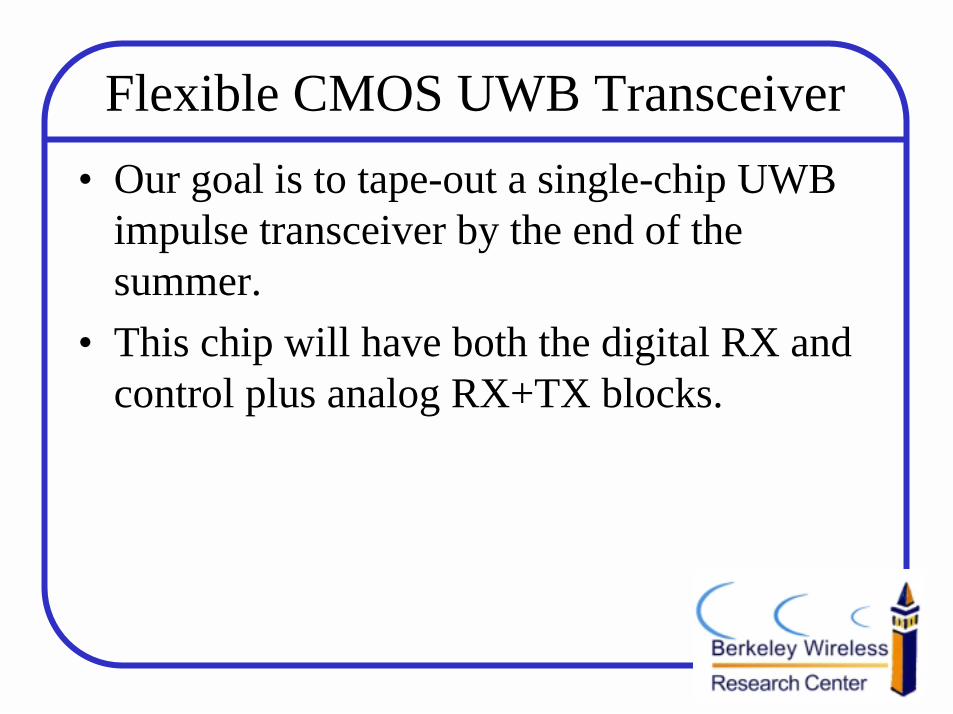
Flexible CMOS UWB Transceiver• Our goal is to tape-out a single-chip UWB
impulse transceiver by the end of the summer.
• This chip will have both the digital RX and control plus analog RX+TX blocks.

Flexibility for UWB system design exploration
– Different antennas (with impedance matching to the LNA)
– Variable transmit power– Variable pulse rates– Digital back-end will contain a programmable pulse-
matched filter– Adjustable data recovery/synchronization blocks – Independent synchronization and data PN sequences– I/O to send the A/D data directly to an external digital
backend (i.e. BEE) for more sophisticated signal processing.

UWB Transceiver Prototype
LNA
PULSE
GAIN andFILTERING
A/DS/H
A/DS/H
A/DS/H
PMF
Data Recovery
SynchDetectAnd
Tracking
CLK GENCONTROL
Goal: Tape-out Single-Chip Transceiver by end of Summer
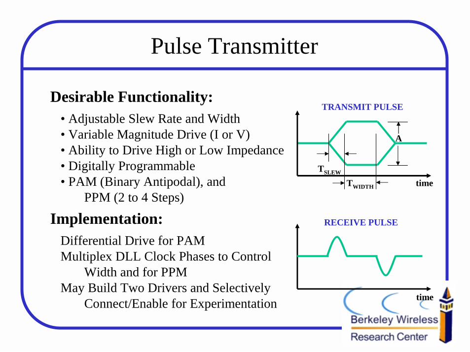
Pulse Transmitter
• Adjustable Slew Rate and Width• Variable Magnitude Drive (I or V)• Ability to Drive High or Low Impedance• Digitally Programmable• PAM (Binary Antipodal), and
PPM (2 to 4 Steps)
Desirable Functionality:
Implementation:Differential Drive for PAMMultiplex DLL Clock Phases to Control
Width and for PPMMay Build Two Drivers and Selectively
Connect/Enable for Experimentation
TSLEW
TWIDTH
A
TRANSMIT PULSE
RECEIVE PULSE
time
time

Pulse Reception
time
time
TSAMPLE
TWINDOW
TPULSE_REP
Parallel Sampling of Window of Time
Three Clocking Timescales:TSAMPLE (<ns) TWINDOW (~10’s ns) TPULSE_REP (~100’s ns)

Antenna-LNA Co-design

UWB Antenna
• Requirements of UWB antennas for our applications– Broadband– Small size– Omni-directional
• Antennas meeting the above specifications do exist, e.g. loop antennas are very good candidates. Large Current Radiator(LCR) is one of them.
• Use EM simulator to characterize the antennas• How about the interface?
– Deem the antenna as a filter and then co-design antenna and circuits

Simulation in EM simulator
• Define the geometry & source• Derives input voltage/current, input impedance,
near/far zone transient fields, s-parameters, animation of the currents/fields/power flow, etc..
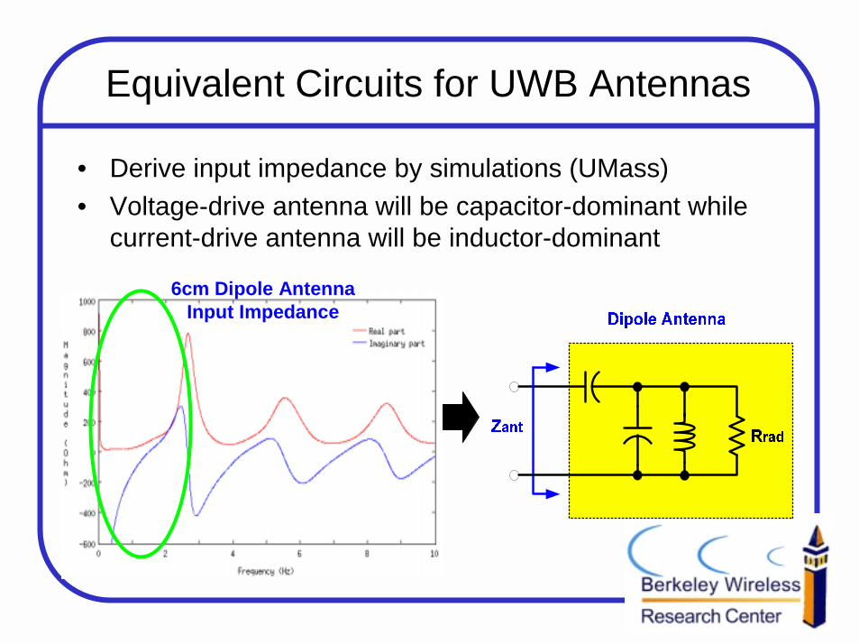
• Derive input impedance by simulations (UMass)• Voltage-drive antenna will be capacitor-dominant while
current-drive antenna will be inductor-dominant
Equivalent Circuits for UWB Antennas
6cm Dipole AntennaInput Impedance

• Compare the far-zone E-fields and the voltage across the radiation resistors of 4cm and 10cm dipole antennas
• Stimulated by a pulse with 50ohm source resistance
Dipole/Monopole Antenna Model
0 1000 2000 3000 4000 5000 6000 7000
-1
-0.5
0
0.5
1
Nor
mal
ized
Vol
tage SPICE
0 1000 2000 3000 4000 5000 6000 7000
-1
-0.5
0
0.5
1
Nor
mal
ized
E-F
ield XFTD Far-Field
0 1000 2000 3000 4000 5000 6000 7000
-1
-0.5
0
0.5
1
Mag
nitu
de
Time Step
0 1000 2000 3000 4000 5000 6000 7000
-1
-0.5
0
0.5
1
Nor
mal
ized
Vol
tage SPICE
0 1000 2000 3000 4000 5000 6000 7000
-1
-0.5
0
0.5
1
Nor
mal
ized
E-F
ield XFTD Far-Field
0 1000 2000 3000 4000 5000 6000 7000
-1
-0.5
0
0.5
1
Mag
nitu
de
Time Step
4cm Dipole Antenna 10cm Dipole Antenna
Aligned Aligned
SPICESPICE
XFDTDXFDTD
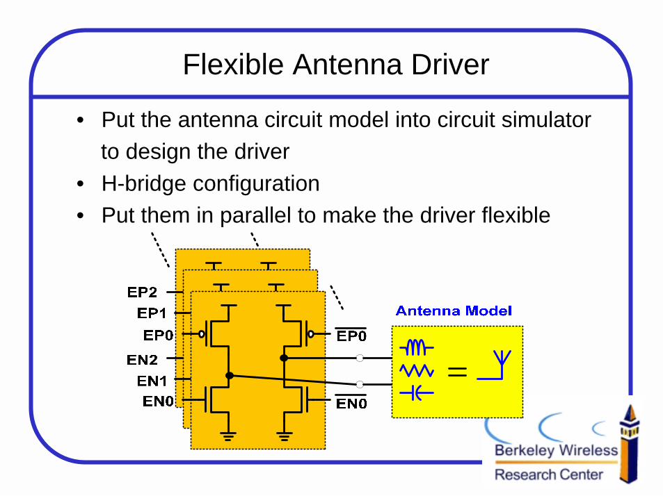
Flexible Antenna Driver
• Put the antenna circuit model into circuit simulatorto design the driver
• H-bridge configuration• Put them in parallel to make the driver flexible

Antenna/LNA Co-design
• Impedance of the Rx antenna seen by LNA is the same as that of the Tx antenna
• Optimize LNA by putting the antenna model in front• Usually voltage-drive RX antennas prefer large ZLNA
and current-drive antennas prefer small ZLNA

Example: Monopole Rx Antennas
• 2cm monopole antenna with different loading• Larger ZLNA gives higher LNA input voltage• Mismatch due to scattering and near-zone field• The relative magnitudes are close
0 2 4 6 8 10 12
-1
-0.8
-0.6
-0.4
-0.2
0
0.2
0.4
0.6
0.8
1
Time (nS)
Mag
nitu
de (V
)
0 2 4 6 8 10 12
-1
-0.8
-0.6
-0.4
-0.2
0
0.2
0.4
0.6
0.8
1
Time (nS)
Mag
nitu
de (V
)
SPICEXFDTD
50KΩΩΩΩ
50ΩΩΩΩ50ΩΩΩΩ
50KΩΩΩΩ

0 5 10 15
0
0.5
1
1.5
Inpu
t Vol
tage
(V)
0 5 10 15-0.04
-0.02
0
0.02
0.04
Time (ns)
Rad
iate
d E
-Fie
ld (V
/m)
Driver Circuit Simulation
• 1ns rise/fall-time input pulse
• Gaussian-derivative-shape waveform of the radiated E-field
• Imperfection of the waveforms due tononlinearity of the driver and coupling between internal nodes
Input Signal
Radiated E-Field
1nS

Driver Circuit Schematic• Inverter chain sharpens the edge of the input signal• Pre-driver NAND/NOR circuits skew the signals
– Enable/Disable the driver – Avoid short-circuit current– Make the pulse radiated more balanced
Input Signal
Driver Enable
Section Enable
Antenna Model
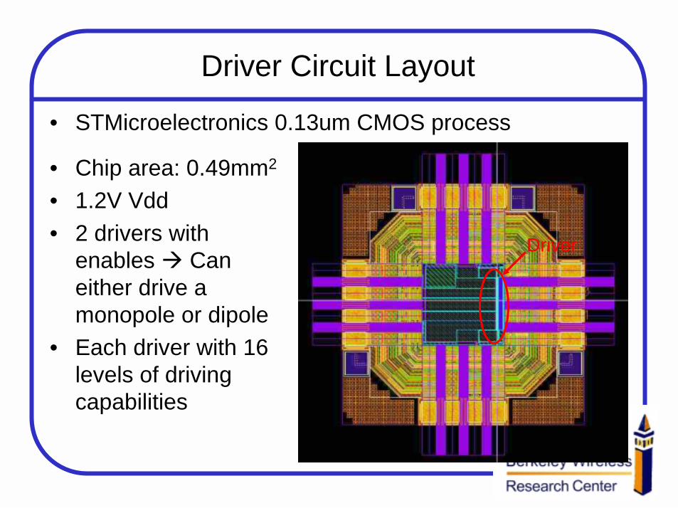
Driver Circuit Layout
• STMicroelectronics 0.13um CMOS process
• Chip area: 0.49mm2
• 1.2V Vdd• 2 drivers with
enables Can either drive a monopole or dipole
• Each driver with 16 levels of driving capabilities
Driver

CMOS Analog Frontend

Timing generation
For Lower Power: Base System Clock on TWINDOWTSAMPLE Derived from DLLTPULSE_REP = TWINDOW / N
DIVIDER
DIVIDER
DLL
DIVIDER
DLL
PLL
TSAMPLE
TWINDOW
TPULSE_REP

Oscillator Accuracy
f = (fTX + fRX)/2 ; ∆f = (fTX - fRX)
⋅≈∆
REPPULSEPN
SAMPLE
TNT
ff
_21
time
Frequency Mismatch Causes DriftTime to Slide One Sample Over One Received Bit; Given Mismatch, Pulse (Chip) Repetition Rate, and Length of PN Sequence.
∆f/f = 2.4 PPMTSAMPLE = 0.5nsTPULSE_REP = 100nsNPN = 1024TWINDOW = 10ns

Oscillator Jitter
time
L100kHz/100MHz = -100dBc
(σ∆T = 100ps)
TSAMPLE = 0.5nsTPULSE_REP = 100nsNPN = 1024TWINDOW = 10ns
∆∆=∆ ∆
Twwww T
2
2
)/( σ
Phase Noise Bound:Maximum Allowable Phase Noise for σ∆T = 100ps (per Oscillator) Over the Reception of One Bit.
L

RX: Clock Generation
VARIABLE DELAY LINE
OSCILLATOR
CHARGEPUMP
&LOOP
FILTER
PHASEDETECTOR
EXTERNALCRYSTAL
TSAMPLE = TWINDOW/N
TWINDOW
BUFFER

RX: LNA
• Gain ~ 10 V/V over ~ 1GHz BW • Noise Figure < 10dB (Not Critical In an
Interference Dominated Environment)• Differential Input • Handle Multiple Antennas (I.e. Current Loop
and/or Dipole)• Switch Bias On/Off within TWINDOW• Fast Overload Recovery (Track Full-
Scale 1GHz Sinusoid)
Desirable Functionality:
Implementation:May Build Two Amplifiers and Selectively
Connect/Enable for Experimentation
-+
-+

RX: Gain + Filtering
• Minimum Gain = 1,000 • Partition Gain/Stages for Minimum
Current Consumption• Capacitive Coupling Between Stages
(Null DC Offset)• Switch Bias On/Off within TWINDOW• Fast Overload Recovery (Track Full-
Scale 1GHz Sinusoid)• Additionally Include Filtering for
Frequencies < 100MHz, > 1GHz• Last Stage Drives Sampling Switch
Load (could be ~100’s fF)
Desirable Functionality:
ON
BIAS
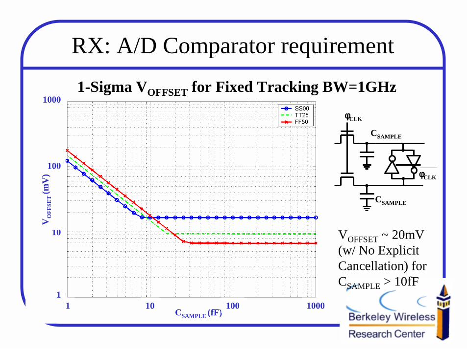
RX: A/D Comparator requirement
1-Sigma VOFFSET for Fixed Tracking BW=1GHz
φφφφCLK
φφφφCLK
CSAMPLE
CSAMPLE
CSAMPLE (fF)1 100010010
1
1000
100
10
VO
FFSE
T (m
V)
VOFFSET ~ 20mV(w/ No Explicit Cancellation) for CSAMPLE > 10fF
Overview of UWB baseband

Specs for Baseband
• Pulse Repetition Rate: 1MHz to 100 MHz• Maximum receivable Pulse ripple length
(Nripple=Npulse+Nspread): < 64ns (128 samples)• Sampling rate: 2 GHz• PN spread ranges from 1 to 1024 chips
PN0 PN1
Nripple<= 64 ns
Trep10ns ~ 100ns

Baseband Overview
CLKA
PMF
Coef
S/P 2568
128PN correlator 1
PN correlator 2
PN correlator 128
fchip
PN GenCLKC fchip
PeakDet
DataRecover
(soft/hard)
Controllogic
Correlation_BlockSymbolStrobe
DataPN
Correlator

Operation Modes• Acquistion mode:
Receiver tries to lock the signal with a certain PN phase. The implementation uses a mixed mode of parallel and serial search, depends on the tradeoffs between hardware and acquisition time.
• Tracking mode: Track the sampling time error caused by the changing
channel, sampling clock offset between transmitter and receiver. If the signal is moving toward the boundary of sampling window, it will feedback a control signal to front end to shift the sampling window. And we take the maximum signal to do data recovery.

Acquisition mode
PN Correlator 1
PN Correlator 2
PN Correlator 128
ADC
•Searching for the peak at the ouput of correlators
Threshold
PMF
From PN generator

Tracking modePN correlator 1
PN correlator 2
PN correlator N
AbsMax
Value
Max Adr
Max Value
Data Recovery
1. Hard decision (symbol detection).2. Soft Sequence detection, such asViterbi decoding.
>
<
AbsMaxAdr
Guard
N - Guard
Ctrl_logic
Feedback tofront end

Control logic
Ctrl_logic
PN correlator 1
PN correlator 2
PN correlator 32
AbsMax
Value
Correlation_Block
PN Code StorageReadaddress
N_block
Strobe_Phase
Disable Signals
•A read clock to fetch the PN phase and a programmable PN length is needed. •Strobe_phase signal is used to define the symbol boundary after entering tracking mode.•A enable/disable control bus is needed for gated clock in PN correlators for power saving purpose.

Simulink Implementation
PMF
PN correlatorsCoef
fsym
PN Generator
S/P

ASIC Design Decisions

Processing Gain
15.6643 dB1.3e-30.86e-340014.4245 dB0.00410.0037300
EbNo @ outputProb. of False alarmProb. of Miss lockChips
• For an Input Eb/No = -11dB 1024 chips is more than enough.(1) Acquisition mode, ~400 chips is enough for suppressing the acquisition error below 1e-3.
2e-51.1e-30.1663BER
20010010Chips
(2) Data recovery mode, ~100 chips could achieve an uncodedbit error rate of 1e-3.

Parallel vs. Serial Acquisition •Assume the worst case using 1024 PN chips, while pulse rate is equal to 100 ns. We need to choose somewhere in between.
(1) Acquisition Time (2) Area Cost
Fully Parallel (0.1 ms)
Serial (0.1sec)
Fully Parallel (500 mm2)
Serial (5.8 mm2)

Partial Acquistion •Once number of parallel search phases are above 10, product of area cost and acquisition time begins to saturate. Not beneficial to increase more search phases. • No. of searching phases is chosen to be 11 in the design.
Reasonable operation region
AreaAcqtime×
Area and power estimation
0
N/A
54.7 uW
N/A
1.14 mW
N/APower(Track)
N/A2.47PN correlators(contain 128 correlators)
N/A<.001Control Logic(state flow)
N/A2.88Peak detector Block(128 inputs)
0.069Data Recovery (Track 3 samples)
10.6Total
N/A.23PN Generator (max 1024 chips)
N/A4.95Pulse Matched Filter (256 inputs, 128 outputs)
Power (Acq)Area (mm2)Block
Area Distribution on Chip•The biggest single block is PMF(Pulse Matched Filter), which is implemented in Carry-save adders.
•PN correlators and Peak detectors are proportional to the number of searching phases. The optimal point makes this area comparable to PMF.

BEE FPGA Array

What’s BEE?• A real time hardware emulator built from 20
high-density Field Programmable Gate Arrays (FPGAs).
• Emulation capacity of 10 Million ASIC gate-equivalents per module, corresponding to 600 Billion operations (16-bit adds) per second.
• Realistic emulation speed 10 – 100 MHz • 2400 external I/O for add-ons, like radios.• Automated design flow from Simulink to FPGA
emulation, integrated with the Chip-in-a-Day ASIC design flow.

Power Board PCB connected to BPU

Simulink - 5120 tap FIR design

5120 Tap FIR filer design (cont.)
80 MHz sample rate.8 Teraops/sec
UWB Transceiver Frontend
60-LVDS Pairs@ 155MHzto the BEE
Receiver1.2 Gsamples/second, 7 bits
TransmitterCMOS H-bridge 2 control bits (LVDS pairs)
from the BEE
VGA and PLLControlfrom the BEE
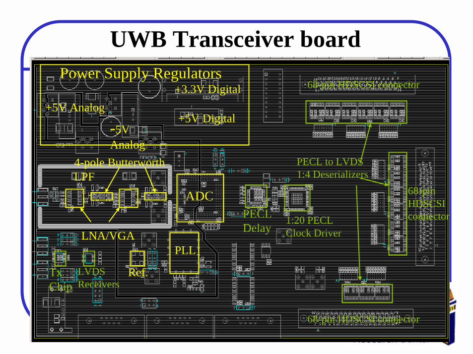
Power Supply Regulators
+5V Analog
-5V Analog
+5V Digital
+3.3V Digital
ADCPECL Delay
1:20 PECLClock Driver
PLL
LVDS Receivers
Tx Chip
PECL to LVDS1:4 Deserializers
Ref.
LNA/VGA
4-pole Butterworth LPF
68-pin HDSCSI connector
68-pin HDSCSI connector
68-pin HDSCSI connector
UWB Transceiver board

Status Summary• First pass system design completed with full
simulations• Analog circuit design approximately 50%
completed• Digital baseband design completed,
backend design beginning• BEE FPGA fabricated and fully functional• BEE UWB frontend designed