![United States Patent [191 4,667,290 Goss et al. May …United States Patent [191 Goss et al. [54] COMPILERS USING A UNIVERSAL INTERMEDIATE LANGUAGE [75] Inventors: Clinton Goss, New](https://static.fdocuments.us/doc/165x107/5f1038da7e708231d4480b4b/united-states-patent-191-4667290-goss-et-al-may-united-states-patent-191-goss.jpg)
'United. States Patent [191 - Google Compute Engine
41
‘United. States Patent [191 Beaupre et al. [11] 4,071,711 [45] Jan. 31, 1978 [54] TELEPHONE SUBSCRIBER DISTRIBUTION SYSTEM [75] Inventors: Donald M. Beaupre, Beacons?eld; Harold A. Ferris, St. Eugene, both of Canada Farinon Electric of Canada Ltd., Montreal, Canada [21] Appl. No.: 588,691 [22] Filed: June 20, 1975 [73] Assignee: Related US. Application Data [63] vContinuation-impart of Ser. No. 494,305, Aug. 2, 1974. [51] m. 01.1 .............................................. .. 1104.1 3/12 [52] U.S. c1. .......................... .. 179/41 A; 179/15 AL; 79/15 BZ; 343/176 [53], Field of Search ....... .. 179/15 AL, 15 Aw, 15 A, 179/15 BA, 15 BM, 15 BZ, 41 A; 325/4, 39, 47, 142, 302, 324; 343/176 [56] References Cited U.S. PATENT DOCUMENTS 3,529,089 9/1970 Davis ............................ .. 179/15 AL 3,562,432 2/ 1971 Gabbard .. .......... .. 179/ 15 BS 3,751,595 8/1973 Moses . . . . . . . . . . . . . . . .. 179/ 15 AL 3,757,050 9/1973 Mizote . . . . . . . . . . .. 179/15 AL 3,786,418 1/1974 Nick ............... .. 179/15 AL 3,804,986 4/1974 Wakamatsu .. 179/15 AL 3,922,496 11/1975 Gabbard .... .. 179/15 BS Primary Examiner-David L. Stewart Attorney, Agent, or Firm—Gowling & Henderson [57] ABs'mAcr This invention relates to a multi-point information dis tribution system useful for telephone service, data con necting systems and other applications which permits a I central station to service a plurality of outlying stations, through transmission media such as radio waves or wire cables, in privacy and using only one transmitting me dium such as a ?rst transmitting carrier frequency and one separate receiving medium such as a different re ceiving carrier frequency. The transmission media cou ples selected input connection points to selected termi nating circuit devices one at a time. In accordance with the invention, the content on input connecting ports ' from a community dial office or other central system is time sampled at the central station which then transmits a sequentially ordered sample stream. Each terminating circuit or device is adapted to receive the content of only one time slot, and to transmit only during a coordi nated and synchronized time slot. The transmissions of the terminating circuits or devices form a sequentially ordered sample stream at the central station receiver which also contains means for distributing the samples into their appropriate central connecting ports. In one embodiment, where the number of outlying terminating circuits is less than or equal to the number of ordered time slots, a separate time slot, and its associated con necting port, is dedicated to each terminating circuit. In a second embodiment, which can service a plurality of outlying terminating circuits greater than the number of ordered time slots, access between any outlying termi- - nating circuit and any time slot is random. The second embodiment uses a traffic control logic means which polls the terminating circuits and assigns time slots to connecting ports and terminating circuits as required. 14 Claims, 11 Drawing Figures
Transcript of 'United. States Patent [191 - Google Compute Engine
‘United. States Patent [191 Beaupre et al.
[11] 4,071,711 [45] Jan. 31, 1978
[54] TELEPHONE SUBSCRIBER DISTRIBUTION SYSTEM
[75] Inventors: Donald M. Beaupre, Beacons?eld; Harold A. Ferris, St. Eugene, both of Canada
Farinon Electric of Canada Ltd., Montreal, Canada
[21] Appl. No.: 588,691 [22] Filed: June 20, 1975
[73] Assignee:
Related US. Application Data
[63] vContinuation-impart of Ser. No. 494,305, Aug. 2, 1974.
[51] m. 01.1 .............................................. .. 1104.1 3/12 [52] U.S. c1. .......................... .. 179/41 A; 179/15 AL;
79/15 BZ; 343/176 [53], Field of Search ....... .. 179/15 AL, 15 Aw, 15 A,
179/15 BA, 15 BM, 15 BZ, 41 A; 325/4, 39, 47, 142, 302, 324; 343/176
[56] References Cited U.S. PATENT DOCUMENTS
3,529,089 9/1970 Davis ............................ .. 179/15 AL 3,562,432 2/ 1971 Gabbard .. .......... .. 179/ 15 BS 3,751,595 8/1973 Moses . . . . . . . . . . . . . . . .. 179/ 15 AL
3,757,050 9/1973 Mizote . . . . . . . . . . .. 179/15 AL
3,786,418 1/1974 Nick ............... .. 179/15 AL 3,804,986 4/1974 Wakamatsu .. 179/15 AL 3,922,496 11/1975 Gabbard .... .. 179/15 BS
Primary Examiner-David L. Stewart Attorney, Agent, or Firm—Gowling & Henderson
[57] ABs'mAcr This invention relates to a multi-point information dis
tribution system useful for telephone service, data con necting systems and other applications which permits a
I central station to service a plurality of outlying stations, through transmission media such as radio waves or wire cables, in privacy and using only one transmitting me dium such as a ?rst transmitting carrier frequency and one separate receiving medium such as a different re ceiving carrier frequency. The transmission media cou ples selected input connection points to selected termi nating circuit devices one at a time. In accordance with the invention, the content on input connecting ports
' from a community dial office or other central system is time sampled at the central station which then transmits a sequentially ordered sample stream. Each terminating circuit or device is adapted to receive the content of only one time slot, and to transmit only during a coordi nated and synchronized time slot. The transmissions of the terminating circuits or devices form a sequentially ordered sample stream at the central station receiver which also contains means for distributing the samples into their appropriate central connecting ports. In one embodiment, where the number of outlying terminating circuits is less than or equal to the number of ordered time slots, a separate time slot, and its associated con necting port, is dedicated to each terminating circuit. In a second embodiment, which can service a plurality of outlying terminating circuits greater than the number of ordered time slots, access between any outlying termi- - nating circuit and any time slot is random. The second embodiment uses a traffic control logic means which polls the terminating circuits and assigns time slots to connecting ports and terminating circuits as required.
14 Claims, 11 Drawing Figures
US. Patent Jan. 31, 1978 Sheet 1 of 8 4,071,711
/ WSQ “RR 8% \ 6E

US. Patent Jan. 31, 1978 Sheet 2 of 8 4,071,711
@N A 8%N.
U.S. Patent Jan. 31, 1978 Sheet 3 of8 4,071,711
1 1%
US. Patent Jan. 31, 1978 Sheet 4 of 8 4,071,711
US. Patent Jan. 31, 1978 Sheet 6 of 8 4,071,711

US. Patent Jan. 31, 1978 Sheet 7 of 8 4,071,711
DA
+ % P0452
’ Rx Bit STRL-‘AM
U.S. Patent Jan. 31, 1978 Sh_eet s of 8 4,071,711
131
4,071,711 1
TELEPHONE SUBSCRIBER DISTRIBUTION SYSTEM
CROSS-REFERENCE TO RELATED APPLICATIONS
This application is a Continuation-In-Part of applica tion Ser. No. 494,305, ?led Aug. 2, 1974.
] BACKGROUND OF THE INVENTION 1. Field of the Invention . This invention relates to an information distribution
system. More speci?cally, this invention relates to such ) a system wherein, with the use of only a single transmit ting medium, such as a ?rst transmitting carrier fre quency, and a single receiving medium, such as a sec ond indifferent receiving carrier frequency, it is possible to service a plurality of outlying stations with a unique and private circuit for any such station. ‘
2. Description of the Prior Art , In one application it is often necessary to provide
telephone service to subscribers who are geographi cally located at‘ points sufficiently remote from. a Com‘ munity Dial Of?ce (CDO) so that the installation of ‘cable for ‘this purpose alone is ‘impractical or not eco nomically feasible. In such cases, telephone service is sometimes'provided by radio links from the CD0 to the subscribers. If a single frequency non-multiplexed sys tem is used to service a plurality of subscribers, then only one subscriber can use the system at any time. In addition, there is alack of privacy under. these condi tions. To overcome these disadvantages, systems are sometimes provided wherein each subscriber station has
, its own transmitting carrier frequency and (a different) receiving carrier frequency. In this way, it is possible for the base station to service more than onesubscriber at a time, and each subscriber loop has privacy relative
‘ to the other subscriber loops. Another way to accom plishithist end is to use this technique in combination withfrequency division multiplex systems. ‘ ‘However, with the second described system, the central station must have as a separate receiver for each outlying station frequency (each subscriber loop), so that the cost of equipment is high, and the use of a
' plurality of frequencies imposes additional'pressures on already overloaded frequency bands. In the version of the systems using a combination of frequency division multiplexing of a transmitted carrier from the central office, some economy of frequencies is achieved but each outlying‘station must be assigned one frequency division multiplex channel and one return radio fre quency so that possibilities of random access still does not exist and utilization of any individual frequency or portion of the-scarce radio frequency spectrum is very
‘
SUMMARY OF THE INVENTION
5
20
25
40
50
55
These and other disadvantages are overcome with ‘ the inventive system which permits servicing of a plu rality of outlying stations (telephone subscribers in this example) with the use of only one transmitting medium such as‘ a transmitting carrier frequency and only one receiving medium such as a different receiving carrier frequency,‘ while still providing a unique and private circuit for each outlying station. It is important to note that the. plurality of outlying stations-may share and separately utilize the system in anadaptive-and as're
60
65
2 aquired manner, thus providing maximum utilization of the two carriers required.
In a speci?c embodiment it is possible to service a greater plurality of outlying stations than the plurality of circuits derived from the two radio frequency carri ers.
In accordance with the invention a multi-point infor mation distribution system comprising a central station and a plurality of physically separated outlying stations, each outlying station comprising at least one terminat ing circuit, whereby said system comprises a plurality of terminating circuits, each said central station compris ing a plurality of connecting ports, and means for cou
' pling selected ones of said connecting ports to selected ones of said terminating circuits one at a time; charac terised in that said coupling means comprises means at
' said central station for time sampling contents of said connecting ports in an ordered sequence during cycli cally recurring time slots to provide, at an output of said time sampling means, a ?rst sequentially ordered sample stream; transmission means at said central station for sending said sample stream directly and in common to each outlying station on a ?rst medium whereby identi-' cal sample streams are sent to each outlying station; receiving 'means at each said outlying stations adapted to receive said sample streams; control means at each said outlying'station coupled to said receiving means to permit only samples in a preselected time slot to be applied to terminating circuits at said outlying stations; transmission means at each said central station and means for providing a signal to said transmission means; said control means comprising means for gating said transmission means only during the time ‘slots of their respective terminating circuits to thereby provide sam ples of said signal, whereby each outlying station trans mits, on a second medium, samples of the signals pro vided to- their respective transmitting means; said outly ing station‘ comprising means for arranging the trans mission time slots at each station relative to one another so that samples will arrive at a receiving means of said central station inia second sequentially ordered sample ' stream; and, distributor means at said central, station connected to an ontput‘of said receiving means and adopted to distribute said time distributed samples onto their respective connecting ports.
BRIEF DESCRIPTION OF THE DRAWINGS The invention will be better understood by an exami
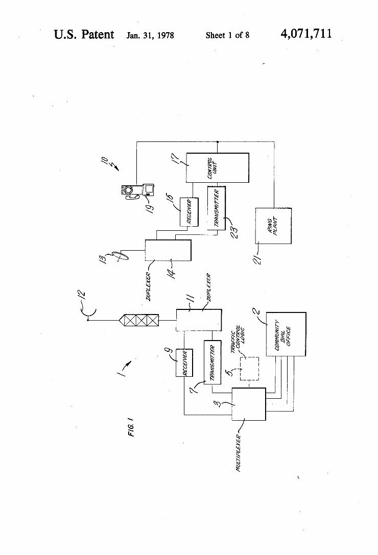
nation of the following description together with the accompanying drawings in which: FIG. 1 is a general block diagram of a system in
accordance with the invention and the speci?c embodi ment wherein the invention may be used to provide telephone service. FIG. 2 illustrates, in block diagram form, a preferred
embodiment of the multiplexer of the system in a spe ci?c embodiment wherein the system'may be used to communicate speech, music or other periodic informa tion. FIG. 3 shows one form of a switching arrangement
which can be used in the multiplexer switching unit, as well as timing circuitry associated therewith; ' FIG. 4 illustrates, inblock diagram form, a'preferred
embodiment of an outlying station; in a speci?c embodi ment wherein the‘ outlying station provides service to a telephone subscriber; _ FIG. 5 illustrates the interconnections of the Traffic '
Control logic unit in a speci?c embodiment related to
‘4,071,711 3
providing telephone service from a central switching of?ce; ‘ _
FIG. 6‘ is a circuit diagram of a specialized circuit used in the system; FIG. 7 illustrates speci?c exemplary circuitry of
blocks 104, 105, 134 and 141 of FIG. 4; FIGS. 8 and 8A and 8B illustrate a preferred circuit
.of the control channel and detector and related wave forms; and FIG. 9-illustrates a preferred circuit
interface.
DETAILED DESCRIPTION OF THE DRAWINGS
In all of the drawings ,the embodiment is shown but
hr the CD0
;not limited to radio waves. Other embodiments are intended to allow the transmission medium to be wire pairs, coaxial cable, modulated light or other suitable means. The essence of the invention is not intended to be con?ned to a speci?c medium of transmission. As one example in the embodiment wherein the invention utilizes wire pairs or coaxial cable, the attennae would be replaced by suitable connecting terminals, and the carrier frequencies would be absent or different than the analagous radio carrier frequencies illustrated. : Similarly, the embodiments illustrated in the ?gures are related but not limited to telephone service. Other similar systems may be illustrated to provide collection of data and condition reports from scattered metering devices or industrial installations, to provide data vtrans mission between computer installations, to provide printingtelegraph service and to provide any other vtypes of communications between scattered outlying stations and a control terminal.
Referring now to FIG. 1, the central station of the system, indicated generally at 1 is associated with a CD0 2, which may be any other type of information center, and includes a multiplex unit 3, which, in one embodiment of the invention is under the control of a
A Traf?c Control Logic (TCL) unit 5. The output of the multiplex unit is fed to a radio transmitter 7 and the output of the transmitter is fed, via a duplexer 11, which, as is well known in the art, separates and directs transmitted and received signals, to an antenna 12. The carrier frequency fl of the transmitter can be any of the frequencies allocated for this purpose by governmental authorities. It is expected that, in Canada, this will be in the 1400 to 1500 MHz range, although technically the system could be used on any part of the radio spectrum where carriers are available. j The base station receives incoming signals at a sepa rate frequency f2, which could be in the same bands as described for the transmitting frequency. The incoming signal is picked up by the antenna 12 and routed, by the duplexer 11, to the receiver 9. The output of the re ceiver is fed to the CD0 via the multiplexer 3. In addi tion, certain data may be fed to the TCL 5.
In accordance with the invention, a plurality of infor mation signals will be presented in parallel to the multi plexer from the CD0 (through vperipheral equipment where necessary) and the parallel signals will be time sampled in sequence to provide a stream of ordered samples at the output of the multiplexer. The periodi cally recurring sampling time slots can then be assigned, one at a time, to pre-selected subscriber stations. Thus, the time slots are analogous to time channels, and each such time channel can bridge the space gap between a connecting port at the central station and a terminating
5
20
25
4,0
45
50
55
65
4 circuit at the outlying station. A system loop consists of any one of the central of?ce-connecting ports bridged to any one of the outlying terminating circuits by a time channel. Each loop circuit is sampled every “m” micro seconds and each loop circuit isusampled for an equal length of time during each cycle, i.e. m/n micro seconds, where n is the number of time slots. The sam pling is, of course, continuous, and the continuous or- - dered stream modulates the one carrier frequency fl. It will, ‘of course, be clear that the number of channels (time slots) corresponds with the number of loop’ cir-_ cuits. - V 1 ,
As will be apparent, the operation, at the central station end, is a TDM system i.e. the output of the n channels is time divided, and the time divided samples are combined to provide a continuous stream which is then transmitted. .v I ..
However, in a conventional TDM system, both re ceiving and transmitting ends of the system each com prises a single physical entity. As will be seen, in accor dance with the invention, a single central station will service a plurality of physically separated outlying sta- . tions. In one embodiment of the invention, the number of outlying stations is equal to, or less than, the number of channels in the system. In this embodiment, each of the channels is dedicated to a predetermined outlying station. In a further embodiment, the'number of outly ing stations is greater than the number of channels. In ‘the further embodiment, at least some of the channels are not dedicated, and access between an undedicated channel and outlying stations is random. , ‘ .
Returning now to FIG. 1,‘ the system further com prises an outlying station, indicated generally at 10. It ‘will .be clear from the above description that the system contains a plurality of physically separated outlying stations, however as all of the stations can be identical, only one is shown in the drawings. Each outlying sta tion- comprises an antenna 13 and a‘ duplexer‘ 14. In addition, each outlying station comprises a receiver portion 15 and a transmitter portion 23. As will be ap parent, the receiver portion of each outlying station will be tuned to the frequency f,, and the transmitter trans mits at the frequency f2. Each outlying station further includes a control unit 17, and‘ in the embodiment shown for telephone service, at least one telephone set 19 and a ring plant 21. a ‘ ~ ‘ I ’
It is noted that each'outlying station may be associ ated with more than one terminating-circuit. A termi nating circuit may consist of either a private line, or all of the telephones ina multi party line, a pay phone line, or any other device required by the system. The control unit at each terminating circuit contains
logic circuitry which operates gating circuitry to allow information to be received only in the correct time slot (i.e. on the current channel) and to enable the transmit ter portion of the station only at the right time and for the correct duration of time, as will be seen below. The preferred embodiment of the invention com- \
prises but is not limited to 16 channels,.and the remain der of the description will relate to such a 16 channel systemalthough it is quite apparent that more or less than. 16 channels could be employed.
- Referring now to FIG. 2, the multiplexer comprises one channel per input connecting port, only one of which is shown in thedrawing. The connecting ports can comprise the outputs of'aCDO interface unit, as will be discussed in relation to FIG. 5. Each input con necting» port in a telephone application comprises. a port
4,071,711 5
of a hybrid 25 which converts the 2 wire telephone signal to a 4 wire signal necessary for radio transmission or for carrying over a cable. The output of the hybrid is ampli?ed in ampli?er 27 and ?ltered in LPF 29. The output of the LPF is fed to the multiplex switch unit 31 where the input information is sampled for equal peri ods of time during equal length cycles. In the preferred embodiment, each input connecting port is sampled once every 125 usec for a period of 7.8 usec. The sampled outputs are fed, in a continuous stream,
to the modulation terminal of modulator means 33. If a pulse width modulation scheme is used, a sawtooth or triangular wave generator 35 would be connected to a second terminal of the modulator 33 as is well known in the art. PWM is the preferred modulation scheme, how ever, it will be obvious that other modulation schemes could be used without departing from the spirit of the invention. The output of the modulator is fed to a ?lter 39
through a control channel indicator generator 37 the function of which will be discussed below. The modula tion signal is then fed to an RF oscillator and modulator 41 of well known construction, and the output of 41 is ampli?ed in the power ampli?er 43 and thence fed to the antenna 12 through the duplexer 11. As can be seen, the items 41, 43 and 11 are in the radio section of the central station.
Received signals are fed, from the duplexer 11, to a down converter 45 (to convert the carrier from an RF to an intermediate frequency), a BPF 47, IF limiter 49 and demodulator 51 in the radio section of the central station. The output of the demodulator is fed to a ?lter 53 and through limiter 57 to the demultiplex switch 59 where the signal is distributed over the appropriate ones
10
20
25
35 of the output connecting ports, each of which contains . an LPF 61 and a part of the 4-2 hybrid 63. The two wire output of the hybrid, constitutes the received voice intelligence for telephone service. Although two separate sets of circuit ports are shown
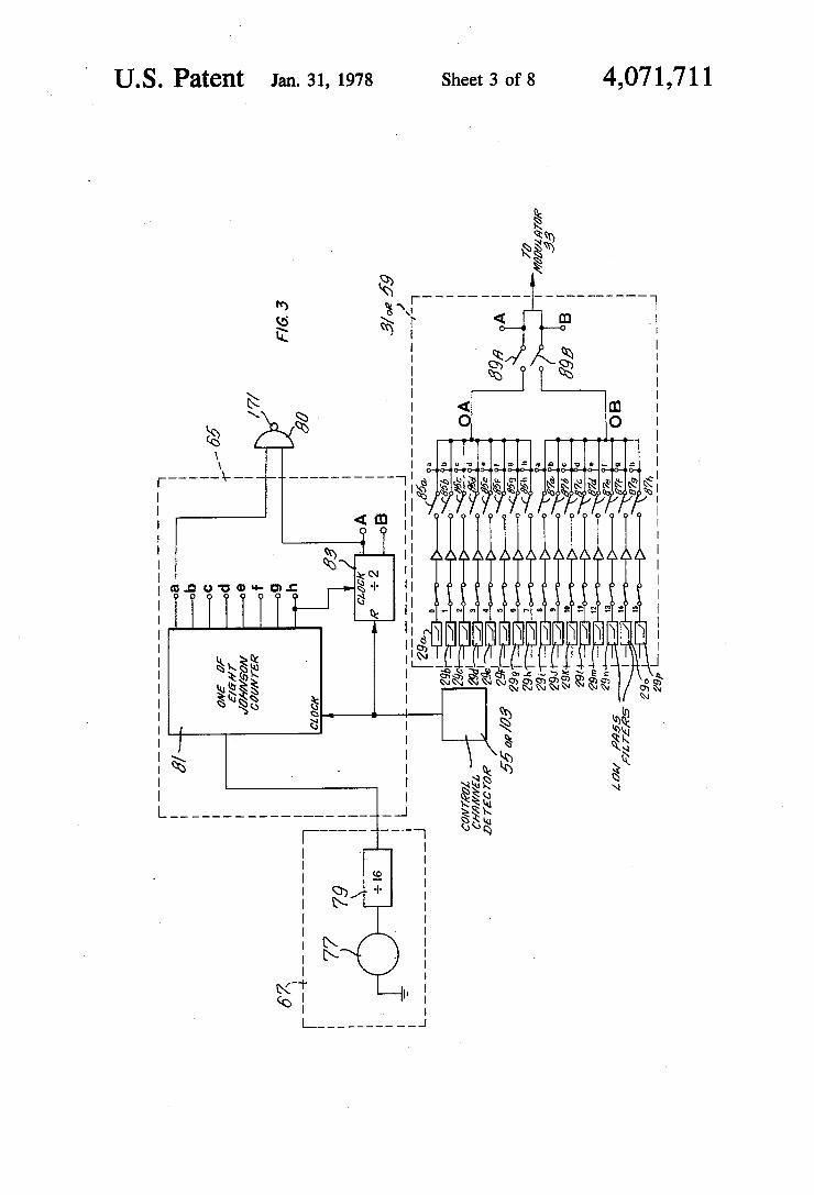
in the drawings, in the physical situation, it may be the same set of 4 wire terminals which are connected at corresponding terminals of both the multiplexer and the demultiplexer. Thus, the input and output loop circuits, while'different conceptual elements, are the same physi cal elements. The drawing illustrates that the system provides separate go and return channels which are normally but not limited to coordinated information. Timing circuitry 65, which receives a clock input from clock means 67, controls the timing of the multiplex and demultiplex switch units 31 and 59 respectively, and it also controls the timing of the modulator means 33 and the control channel indicator generator means. In the preferred embodiment, the control channel indicator is simply an “exalted” pulse, i.e. a pulse of greater ampli tude than the other pulses of the system. Obviously, other indicators could be used. A circuit diagram of one form of the multiplex switch
unit along with the associated part of the timing cir cuitry and the clock means is shown in FIG. 3. The FIG. 3 circuit is of the type used with a 16 channel system with a cycle of 125 usec and a sample length of 7.8 usec, as in the preferred embodiment.
Referring to FIG. 3, the switch units are contained within the dashed line box labelled 31 or 59, the timing circuitry is contained within the dashed line box la belled 65, and the clock circuitry is contained within the dashedline box labelled 67.
45
50
55
60
65
6 The clock consists of an oscillator 77 whose output
frequency is 2.048 MHz, and a divide by 16 frequency divider 79 which provides a pulse output after counting the 16 leading edges of input pulses. Thus, the output of 67 is a pulse wave with a frequency of 128 kHz, i.e. one pulse every 7.8 usec. The timing circuitry comprises a one of eight John
son counter 81 having eight output leads “a” to “h” and one input lead. In operation, a high appears at only one of the output leads at any one time. When a pulse is applied to the input, the high moves to the next lead down. When the high is on lead “h” and a pulse is ap plied to the input, the high will move to the “a” lead and start a new cycle. The timing circuitry also includes a ?ip-?op 83 having a clock input terminal and a reset input terminal, as well as A and B output terminals. As is well known in the art, a high will be present on
only one of the A or B terminal at any one time. The multiplex switch unit consists of a ?rst plurality
of eight lines 0 to 7, each interrupted by switch means 85a-to 85h respectively, and a second plurality of eight lines, 8 to 15, each interrupted by switch means 87a to 87h respectively. As can be seen each line is connected, at one end thereof, to a separate connecting port. In addition, each of lines 0 to 7 contain terminals 0 to h respectively, and ‘each of lines 8 to 15 contain terminals a to h respectively. Each of these terminals are sche matic representations of control means for their respec tive switches, and each control means a to h is con nected'to outputs a to h of the counter 81 respectively. The control means operate in such a way that, when the output to which they are connected is high, the switch they control will be closed. The lines 0 to 7 are connected together at the output
ends thereof, and the junction of these lines is connected to a further line 0A, which is interrupted by switch 89A. In a like manner, the lines 8 to 15 are connected to gether at their output ends, and the junction thereof is connected to line 0B which is interrupted by switch 89B. The output ends of lines 0A and 0B are connected together and the junction thereof is connected to the modulator 33 of FIG. 2. Lines 0A and 0B contain termi nals A and B respectively which comprises .the control means for switches 89A and 89B respectively and which are connected to output A and B of ?ip-?op 83 respectively. Each switch is closed when a high is ap plied to its control means.
In operation, the above described circuits operate as follows: Assuming a high is present at output g of counter 81, and that a high is present at output A of the ?ip-?op, it can be seen that switches 85g, 87g and 89A will be closed. Thus, the output of connecting port 6 will be applied, through closed switches 85g and 89A to the input of the modulator. None of the other connect ing port outputs will be applied to the modulator as switches 85a to 85f and 85h are open so that the inputs of lines 1 to 5 and 7 cannot‘ reach line 0A. Similarly, as line 0B contains open switch 89B, the output that reaches it on line 14 through closed switch 87g will not be applied to the modulator. Thus, the data on only one connecting port reaches the modulator.
After 7.8 usec, a pulse is applied to the counter 81 so that the high moves to output h. At this time, only the output of connecting port 7 will reach the modulator. After a further 7.8 usec, a further pulse will be applied to 81 so that a high will appear at output a thereof. In addition, the lagging edge of the pulse at output h will set the ?ip-?op so, that a high appears at output B
4,071,711 7
thereof. Thus, switches 85a, 87a and 89B are closed. At this time, only output of connecting port 8 will reach the modulator over line OE. With the above circuitry, each connecting port is
sampled for a period of 7.8 usec once every 125 usec. In addition, the output of the multiplexer is a continuous stream of the sampled outputs.
It is, of course, understood that the above-described circuitry comprises only one circuit for carrying out the timing and multiplexing functions and that other cir cuits can also be used for these purposes within the spirit and scope of the invention. FIG. 3 also illustrates how the control channel detec
tor can be connected to the timing circuitry and the operation of this detector will be described below. An outlying station, which will operate in conjunc
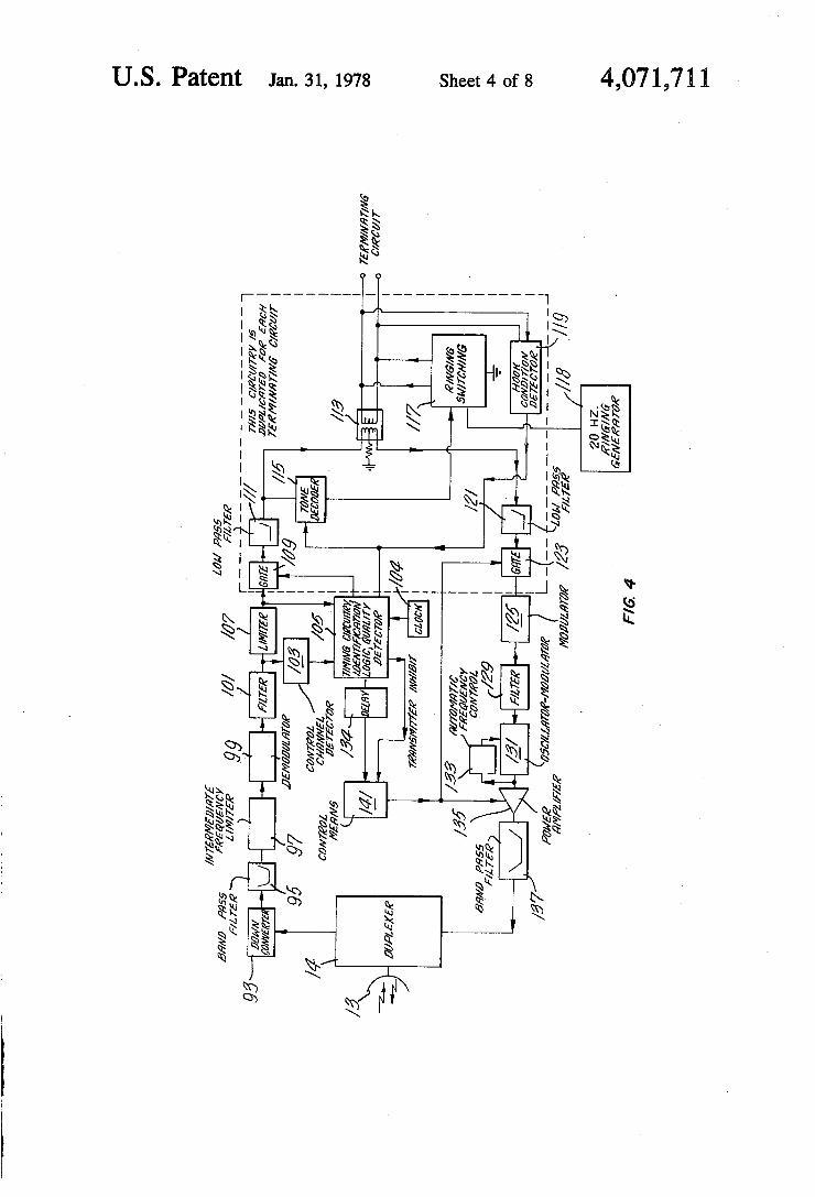
tion with a central station as above-described, is shown in FIG. 4. The outlying station illustrates a telephone subscriber application but is not limited to this applica tion. The control station consists of two main parts; The radio and control section on the left hand side of FIG. 4 and the line terminator circuitry as required enclosed in the dashed line box at the right hand side of the ?g ure. The line terminator circuitry illustrated is speci?c to a telephone subscriber loop. Other appropriate line terminator circuitry would be provided for other types of information circuits. Each outlying station can service more than one
terminating circuit. The radio and control part is com mon to all terminating circuits, but a separate line termi nator is provided for each terminating circuit. As each line terminator may contain the same structure as every other line terminator, only one is shown and described in FIG. 4. The output of the duplexer 14 is fed, via down con
verter 93, BPF 95, IF limiter 97, demodulator 99, ?lter 101 and limiter 107 , to the gate 109 of the line termina tor. At thesame time, the output of the ?lter 101 is fed
_ to a control channel detector 103 whose output is fed to the circuitry box 105 which contains timing circuitry, logic circuitry, and quality control circuitry. The clock is preferably a VCO under control of circuitry in 105. Circuitry 105 will also examine the quality of the re ceived signal and, if it falls outside predetermined limits, circuit 105 will inhibit the transmitter.
In the telephone line terminator shown, the tone decoder 115, fed from LPF 111, detects a ringing signal when it is present and actuates the ringing generator 118, through ringing switching 117, which sends a 20 Hz ringing signal down the subscriber loop line, when such a ringing signal is present. A tone, rather than a DC is used as a DC signal cannot be sent over the radio link. The 4 wire signal is converted to a 2 wire signal in the
hybrid 113 for voice communications with the sub scriber loop. -
In the transmit direction, the hook condition detector 119, which can merely be a DC detector as well known in the art, determines whether the subscriber loop is in the ON or OFF hook condition. If the loop is OFF hook, then the detector will provide a signal which will inhibit the tone detector so that it cannot actuate the ringing generator. At the same time, it will provide a signal to the circuit 105 which will then generate an appropriate code for transmission to the base station.
_The voice signal is again converted from a 2 wire to a 4 wire signal in the hybrid 113, and the 4 wire signal is then fed, through LPF 121, Gate 123, modulator 125,
15
25
35
40
45
50
55
65
8 ?lter 129, RF oscillator-modulator 131, power ampli?er 135, and LPF 1337, to the duplexer 14 and to the an tenna 13 for transmission. AFC 133 can comprise any appropriate circuit well known in the art for providing the automatic frequency control function.
Control means 141 performs the function of insuring that the transmitter is inhibited at all times other than its appropriate transmission time slot as will be discussed below. Means 141 can be a shaped pulse generator whose output will key the power ampli?er and open the gate 123. As can be seen, 141 is actuated byy the timing circuit 105. Delay 134 compensates for the differences in distance
between the different outlying stations and the central station. As will be seen, it is essential that the signal from an outlying station arrive at the central station in its proper time slot. By providing different delays in the different outlying stations, the relative timing as be tween the outlying stations, vis-a-vis the time of arrival of an outlying station signal at the central station, is controlled.
It is contemplated that each outlying station will be ' able to service up to six terminating circuits. A simpli?ed block diagram of the traf?c control logic
is shown in FIG. 5. As can be seen, the unit consists of ?ve basic building blocks; A read only memory 147 An input/output buffer 149 A random access memory 151 A processor 153 A CDO interface 143
which may be any other information center. ' The read only memory is preferably a non-volatile
memory unit which will contain the sequence of opera tions of the rest of the TCL. The input/output buffer allows the TCL to accept data arriving on the incoming stream and to inject data on the outgoing stream. The random access memory is used as a temporary store to store such information as the addresses of outlying sta tions presently handling traf?c, and which channel number they have been assigned. , The processor generates signals to operate the
switches in the CD0 interface unit at the right time and in the right sequence. The CD0 interface contains a matrix array of bi-lateral switches under the control of the TCL which provide interconnections between the VF channels of the CD0 and the subscriber loops for a telephone application.
Control bus 155 carries the control signals from the ROM to the I/O buffer, the RAM and the processor. Data between the building blocks is moved over the data bus 157. The functions of the TCL will be de scribed below. As will be seen, the design of the circuits for implementing these functions is within the normal skills of one skilled in the art, and such design does not constitute a part of the invention. However, to better teach the invention, Appendix “A” hereof provides a more detailed description of the TCL. Appendix “B” includes an instruction set for the pro
cessor, while Appendix “C” and “D” illustrates a pre ferred ?ow chart of a program for controlling the pro cessor and an instruction listing of the program respec tively.
In considering the operation of the inventive system, there are two separate embodiments whhich must be examined:
4,071,711 .9
a. ‘The (dedicated channel system wherein the number ,of outlying terminating circuits is less than or equal to the number of system channels; I
b. The random access system wherein the number of outlying terminating circuits is greater than the number of system channels. .
- In the dedicated channel system, there is no require merit for the TCL, as outlying stations do not have to be polled, and a decision does not have to be made as to which channel should be assigned to which terminating circuit. In addition, as the number of terminating cir cuits is less than or equal to the number of time chan nels, the number of VF channels from the CDC is also lessthan or equal to the number of time channels. Thus, the VP channels from the CD0 can be connected di rectly. to the terminating circuits so that a CD0 inter faceis not required.
' InHthe dedicated channel system, each connecting port and terminating circuit is assigned a speci?c time
_ channel or time slot. It is only necessary that the clock and counters of the outlying station remain in sync with the clock and counters at the master station, and to this end,‘ ‘104 is a VCO under the control of circuitry in 105.
In the central station, the input channels are sampled at a predetermined rate, say in 125 psec cycles, with the width of each sample being substantially identical to the width of every other sample, e.g., with 16 time chan nels,.sample width is 7.8 usec. The samples are then combined into asingle stream with one sample follow ing the otherQThis is, of course accomplished in the multiplex switch 31 as described above. The stream then. modulates an RF carrier, and the modulated RF ‘Carrier energizes the antenna .12 for transmission of the modulater carrier. The transmitted signals will then be received by all, antennas 13 of all outlying stations. However, timing circuitry 105 will open gate 109 only in the time slot withwhich the terminating circuit is associated. Thus, only the samples of the time slot asso ‘ciatedwith this terminating circuit will be supplied to “the circuit terminating or telephone equipment. The LPF 111 asis well known in theart, will connect the individual samples at each terminating circuit gate into a continuous analogue signal which is converted, in hybrid 113,‘from a 4 wire to a two wire signal which is thentransmitted to the circuit terminating or telephone equipment. In a telephone application, ringing tones willbe detected by the tone decoder to actuate the ringing generator when a ringing signal is transmitted from .the base station. Through control channel detector 103 therewill be a
‘connection between the output of ?lter 101'and timing circuit 105 to insure synchronization of counters in 105 with the counters at the central station. It is noted that inorder for the timing circuit of the receiver portion of the outlying station to be in system. sync, it will most likely be out of sync in real time with the timing circuit of the central station as the signal transmitted by the central station in the time slot of the terminating circuit willarrive at the outlying station some time after it has been transmitted. Thus, to be in system sync, the timing circuit of the receiver section ,of the outlying station will'have’to lag the timing circuit at the central station.
4 Synchronization of the timing circuitryat the outly ing station with the timing circuitry at the central sta tion is accomplished as follows: at the central station, an eiralte'd pulse is periodically sent out in a predetermined
; time slot. Preferably, the predetermined time slot is the gerp time slot. The'exalted pulse could then be sent out,v
20
25
30
35
40
45
60
65
'10 say, every cycle, or every 5th cycle, etc. At the outlying stations this exalted pulse will reach the timing circuitry 105 via the Control Channel Detector 103 (FIG. 4) and can be used to reset the clock (as will be explained below with reference to FIG. 6) if the outlying station is out of sync. The connection 103 between the output of 101and
the input of 105 will also feed a signal to the quality detector part of 105 and, if the quality of the received signal falls outside predetermined limits, the transmitter of the outlying station will be inhibited.
In the described telephone application, on the trans mitter side, the telephone will be either ON or OFF hook. If it is OFF hook, the subscriber will usually be either talking or dialling a number. As mentioned above, the transmitter is keyed only in
the time slot allocated to the terminating circuit in ques tion. The distance between the stations must be taken into account. As the signal from the central station is sent some time before this time slot is received at the central station, in order to be in system sync, the timing circuit of the transmitter portion of the outlying station will have to lead the timing circuit of the central station. The amount of time that a transmitter is keyed to be on, will be equal to the sample width at the central station, and the period of cycling at the outlying station trans mitter will be equal to the period at the base station.
Voice‘signals will also be keyed so that what is trans mitted is in effect, samples of the voice signal. When an outlying station is servicing more then one terminating circuit, the transmitter will be keyed in the time slot of all the terminating circuits active in this period. How ever, circuit gate 123 will be keyed only during the time slot of its respective terminating circuit. These samples arrive from the different outlying stations to the central station in their respective time slots so the signal fed to the receiver at the central station comprises a stream of samples ordered in the sequence of the time slots. The stream is then split up into the respective connecting ‘ports in the demultiplexer 59 so that each connecting port at the end of the central station receiver contains only data from its assigned terminating circuit. The content at each port will again be a series of samples which will be processed, in manners well known, to form an intelligible audio signal or data stream. With the dedicated channel system, a time slot is
always available to each terminating circuit and the time channel is predetermined. Thus, when the central station has to communicate with an outlying station, the central station knows exactly where to go.
In the random access system, the time channels or time slots are not so assigned. In order for the central station to maintain control over the outlying stations, the central station polls the outlying stations one at a time to determine their status and to acknowledge any of their requests. The polling of the outlying stations comes under the control of the TCL. . The polling activity requires that each terminating
circuit be separately and uniquely identi?able. Accord ingly, each terminating circuit is assigned a unique code. The code can be an eight bit binary code which provides 256 different identi?ers. More or less bits could be used depending on the requirement, or codes other than binary codes could be used for identi?cation purposes. In any case, the code is generated at the cen tral station under the control of the TCL. To poll an outlying station, the central station ?rst
sends out the identifying code of the station. It will, of
4,071,711 11
course, be appreciated that, if the code is an eight bit code, it will require eight sampling cycles just to trans mit the code. However, as a cycle is only 125 usec, the amount of time required for transmitting the full code is only‘ 1.0 msec. The code is transmitted on a control time slot or
channel. This is any arbitrary, unused channel selected by the TCL. Data transmitted on this channel is contin uously monitored by all outlying stations regardless of their circuit demand conditions. The TCL, when it selects a control channel, will transmit a control chan nel identi?er code on that channel to alert all outlying stations. The code can be simply an exalted pulse. The identifying code of a polled station is then transmitted, and each outlying station will examine the code in the identi?cation logic 105 of the outlying stations. Only the terminating circuit identi?ed by the code will react as described below. The remainder of the terminating
‘ circuits will await the reception of the respective codes. It will, of course, be appreciated that when an outly
ing station services more than one terminating circuit the identifying codes of each terminating circuit will be stored in 105, and 105 will contain separate control outputs for respective gates 109 of the terminating cir cuits under its control.
After the outlying station successfully decodes its code, the transmitter of the terminating circuit will be opened long enough to permit the terminating circuit demand status to be transmitted. Then the transmitter is again inhibited. While awaiting aresponse from the outlying station, the TCL examines the connecting port from the CDC to see if a circuit demand is present. If this demand is not present, and the terminating circuit reports no circuit demand condition, then the central station will poll the next outlying station terminating circuit. In this regard, the identifying codes of the termi nating circuits are contained in the ROM in sequence and the stations will be polled in this sequence.
If there is a circuit demand, such as a ringing signal present from the CD0, or if the terminating circuit reports a circuit demand such as an off hook condition, this indicates that a connection is required. The TCL will now poll the terminating circuit a second time and, when the second successful decoding is accomplished, the logic circuitry of the outlying station will cause the terminating circuit to lock onto the control channel so that this terminating circuit will receive transmissions in this time slot. Of course, the transmitter port of the terminating circuit will also be synchronized onto this channel, so that the terminating circuit will transmit in this time slot. The control channel is now carrying traf?c, so that it cannot be used for control purposes any longer. The TCL will accordingly select another channel
which is not handling traf?c as the new control channel. Again, a control channel identi?er is transmitted and all outlying stations will monitor the new control channel. While the polling is taking place, the committed time
slots will be carrying traf?c to their respective terminat ing circuits.
Besides the functions already described, the TCL will monitor all assigned channels for the reception of RF carrier in the time slot. When this carrier disappears for whatever reason, the
TCL will cease its normal polling sequence, and will poll the outlying terminating circuit which had been assigned the time slot, using the control channel.
10
25
40
45
50
60
65
12 - If this is successfully decoded by the outlying station, its transmitter will be enabled long enough'to reply with circuit demand status, then shut down. it‘ Under normal conditions the carrier will have disap
peared because the communications had terminated and the circuit demand had disappeared. In this event no circuit demand will be received to the poll,‘and the channel will be available for reassignment. ' :
However, abnormal or malfunction conditions could have caused the carrier to disappear. Some of these conditions and corrective actions follow:
i. A deep prolonged fade in direction central to outly ing station or failure of outlying station receiver. This would be sensed by the quality detector and cause the~outlying station TX to shut down as above-described. While the condition perists there will be no response to a poll. This will cause an alarm condition to be logged at the base station.
. A deep prolonged fade in the direction outlying station to central or failure of outlying station transmitter. ~
This would result in failure to respond to a poll, , and give rise to an alarm at'the central station.
iii. Loss of synchronization at'the outlying station. If this were due to fading or Rx failure this would be covered by case (i)., ‘ '
However, if some other cause resulted in jumping synchronization, polling the outlying station would bring him back into synchronization and ‘force him on to the control channel. , ‘
This response to the ‘poll'would be a circuit de mand condition, in which case he would be re polled as described above and the circuit re-estab lished. ' A
As was mentioned above, any type of modulation can be used. However, PWM is preferred primarily due to the fact that this type of modulation has greater echo immunity. '
Another bene?t derived from using PWM is that it readily provides a means of maintaining system syn chronization. Periodically a ‘time slot, in addition to being width modulated, is also simultaneously ampli tude modulated. This is the above referred to Exalted Pulse. ' ‘
The mechanics of maintaining synchronization are as follows: '
When the central station counters are at zero, the Exalted Pulse Generator circuit (37 in FIG. 2) is acti vated and the positive portion of the information pulse within the 7.8 uS time slot is increased’in amplitude. At the outlying station, an Exalted Pulse detector (103 in FIG. 4) senses the presence of this pulse by‘ slicing off the bit stream at a predetermined level, and this pulse is used to force the counters of the outlying station timing circuit to zero. Special circuitry is used to differentiate between a genuine exalted pulse and anoise impulse, so that noise bursts do not erroneously set the system. One circuit is shown'in FIG. 6. '
In FIG. 6, 159, 162, 163 and 167 are two terminals NAND gates. NAND gates 162 and 167 are connected as inverters. 165 is a monolithic timing circuit and R and C are a resistor and capacitor respectively having a time constant somewhat longer than the time between Ex alted pulses. Terminal 169 is connected to the output of control channel detector 103, and terminal 171 is con nected to the circuitry of 105 and would go true when the counters are at zero. This would be the output of AND gate 80 of FIG. 3 when such a timing circuit is
4,071,711 13
used. Terminal 173 is connected to the RESET termi nals of the counters in the timing circuitry of 105 (FIG. 4).
In operation, the circuit works as follows:v Capacitor C is charged through resistor R and the time constant of RC is so chosen that, if C is charged for a period of time less than or equal to the time between exalted pulses, it will not charge up to a high enough value to trigger timer 165. When the outlying station is in sync, then pulses will arrive at terminals 169 and 171 at the same time. Gate 163 is normally closed so that output from 169 arriving at this gate will not be permitted to pass. However, when the pulses arrive at both inputs of gate 159, it will provide an output which will turn transistor 161 on. The capacitor C will discharge through the turned on transistor and, after gate 159 closes to turn off transistor 161, the charging cycle will begin again. As can be seen, under these conditions, no signal is pro vided at terminal 173 so that the timing circuitry re mains unaltered.
If, however, the outlying station is not in sync, then the exalted pulse will not arrive at terminal 169 when the frame pulse arrives at 171. Thus, no signal will be provided to transistor 161 to turn it on so that there be no discharge path for capacitor C. Thus, the capacitor will charge up to a large enough value to trigger the timer 165. This will open gate 163 via inverter 162, to allow passage of the next exalted pulse which arrives. Thus, the next exalted pulse will pass through gates 163 and 167 to reset the counters of timing circuit 105 to the control channel. The outlying station is now in sync so that the next exalted pulse which arrives will corre spond, time-wise, with the frame pulse. The output of gate 159 at that time will discharge capacitor C by turning transistor 161 on. At the same time, it will reset timer 165 which through inverter 162 will close gate 163.
In the above, only radio waves have been considered as the coupling. means between the central connecting ports and the terminating circuits. As has been men tioned above, it is also possible to use conductor cables as the coupling means. In some cases, it may be feasible to use a cable pair for these transmission purposes. In such cases, different carriers could be used for transmit ting from the central station and for receiving by the central station. This is so that only one pair of cables would be needed for transmission in both directions. Usually, the carrier frequencies are chosen different from the frequencies used in the case of radio wave coupling, but in all other respects, the systems are simi lar. However, the invention is particularly useful when
cables are already available between a central station location and a plurality of outlying locations. These cables may be carrying TV and radio signals, as well as other communications data. In this situation, it is con templated that the various different signals may be fre quency division multiplexed, i.e. each different signal would be carried by a different carrier frequency and the several carriers would be carried by the same cables. One or more of such different carriers may be modu
40
45
55
60
lated by the inventive system. Techniques and equip- ' ment for frequency division multiplexing and demulti plexing are well known in the art and do not constitute a part of this invention, and the remainder of the system would be similar to the system wherein the coupling means are radio waves.
65
14 Although the system has been described for use with
a telephone network, the same system can be used to distribute other types of information and data. As will be apparent, when other data is distributed, the inputs and outputs will be different. Thus, considering FIG. 2, all of the equipment to the left of the multiplexer-demul tiplexer line would be changed. But, the equipment to the right of the line does not change in principle when different information or data is distributed.
In a like manner, the equipment in the dashed line box in FIG. 4 would change with a change in data. But, the equipment outside of the dashed line box is not changed. The invention has above been described in general
terms and should provide one skilled in the art with enough instructions for practising the invention. Never
_ theless, exemplary embodiments of certain portions of the inventive system are described below to better in struct one skilled in the art in the practice of this inven tion. Turning ?rst to FIG. 7 of the drawings, illustrated in
FIG. 7 are speci?c and exemplary circuits for accom plishing the requirements of the blocks identi?ed as 105, 134 and 141 of FIG. 4.
Considering ?rst the timing organization of the sys tem, in the preferred embodiment discussed above, there are 16 time slots each approximately 7.8 p. sec wide used to communicate between the central and subscriber stations. The grouping is such that 16 consec utive time slots, one of which is the control slot or channel, constitutes a subframe of 125 )1. sec duration. Eight subframes' make a half frame of 1 msec and, of course, 2 half frames give a frame of 2 msec. The very ?rst pulse at the start of each full frame sent
by the central station is marked and recognized by all subscriber units at the outlying stations to ‘indicate to
' them that (a) this is the control channel, and (b) it.is the start of a polling sequence.
In this system, one channel (time slot) is always used for control purposes and handles digital information only. The remaining 15 channels handle the message path information and are assigned as required on a fully random access basis between all subscribers forming part of the system. As will be clear, this is a system wherein the number of subscribers is greater than the number of time slots or channels available sothat the TCL is in operation.
All subscribers who have not been assigned a channel are interogated or polled sequentially by the central station sending out the subscriber 7 bit binary address.
Thus, the ?rst pulse of the whole frame is a sync pulse on the control channel. The address of the subscriber station under interogation is transmitted in the control channel time slots of the next 7 sub-frames at the rate of one bit per sub-frame. Hence, by the end of the ?rst half frame, the interogation of one subscriber is complete. During the second half frame the central station awaits for the subscriber to decode the transmitted address and to make the reply of his hook status, which is sent back over the control channel.
Referring now to FIG. 7, the bit stream, in its en tirety, and identical at all subscriber stations, splits in two ways. In one path, it goes to the OR gate 206 and from this path the address information will be‘ extracted as described below. I
In the second route, the bit stream is fed to a phase locked crystal oscillator 201, running at a nominal fre quency of 2.048 MHz. The phase- lock oscillator is of the type which is well known in the art and needs no fur
4,071,711 15
ther description here. The 2.048 MHz. signal emerging from the locked loop is at precisely the same frequency and has a ?xed phase relationship to its counterpart master oscillator at the central station. The 2.048 MHz signal is divided by 16 in divider 202
to give a 128 KHz signal (hereinafter referred to as 128 Rx) which is the clock signal used to advance the re ceived counters. The 128 Rx is divided by 2 in divider 229 to give a 64 KHZ reference signal which is com pared with the received bit stream in the phase lock loop. The 128 Rx signal also clocks a divide by 16 counter
216 which gives an output every sub frame. Since this last divider is reset to zero by the sync pulse via FIG. 6 circuitry as described above, it follows that the pulse at the output of this divider (which is marked CON in FIG. 7), identi?es that the information on the receive bit stream at this time is control channel information. By using the CON signal to clock a 7 stage shift register 210, the digital address information is fed into the regis ter during the ?rst half frame. The CON signal is also used to clock another divide
by 16 counter 217 which counts the 16 sub frames to give an output pulse at the start of each complete frame. This output is marked FRAME PULSE in FIG. 7. The 128 Rx clocks a l of 8 Johnson counter 213 and
the last stage of the Johnson counter clocks a ?ip ?op 214. The number 7 output of 213 and the “Q” output of 214 are two of the three inputs to AND gate 215. The output of gate 215 controls the receive gate switch (item 109 of FIG. 4). However, unless the station has been assigned a mes
sage channel, the third input to gate 215, marked CON NECT, will be low and the gate will remain blocked.
It is also noted that the reset pins of counters 213 and 214 are connected together and the reset is activated indirectly from the sync pulse, as will be later described. It has already been shown that the counters, dividers,
, and ?ip ?ops consisting of the parts labelled 229, 216, 217, 213 and 214 are all clocked either directly or indi rectly from a common signal called 128 Rx which has a frequency and phase relationship ?rmly tied to the mast oscillator clock at the central station. Also, each of the above devices using a reset pin are reset to zero at a time derived directly or indirectly from the sync pulse which is generated and sent from the central station when the central station clocks are at zero. As above discussed, in the basic system design, infor
mation from a subscriber is expected to be received at the central station in the same time slot as information sent to the subscriber from the central station, whether this be data information via the control channel or mes sage information over an assigned message channel. Irrespective of the media used to transport the informa tion, it takes a ?nite time to traverse the distance be tween the central and subscriber stations in each direc tion.
In the direction central to subscriber, timing synchro nization is relatively simple since the sync pulse used to maintain sync is transported to the subscriber over the same medium as the bit stream and thus suffers the same delay as the message or data information. However, in the direction subscriber to central station, the transmit ted information must be delayed by a ?nite period of time with respect to the received time slot to ensure that the subscriber information arrives at the central station in the correct time slot but an integral number of sub frames later.
5
20
35
40
45
65
16 The required delay time is a direct function of the
path length and is set by the circuitry of block 134 of FIG. 4 which is shown in more detail in the dotted line labelled 134 in FIG. 7. As can be seen, this includes a variable delay (?ne) means 203, a ?ip ?op 204, and AND gate 207. To understand how the means 134 operates. it must
be recalled that the counters 213 and 214 control the timing of the received signals. A signal delayed with respect to. the received time slot is derived by AND ING one of the 8 outputs of the Johnson counter 213 with either the Q or Q signal from the ?ip ?op 214, in the AND gate 207. By the nature of the circuit, this delay can only be incremented in 7.8 microsecond steps, and these strapping options are referred to as the COARSE TIMING ADJUSTMENTS. To obtain the precise delay required, the output of
AND gate 207 is applied to the DATA input of the ?ip ?op 204 at a point shortly ahead of the time that the transmitter is required to operate, and is clocked out of the ?ip ?op at the exact time required. The clock pulse for the ?ip ?op 204 is derived from ‘
the circuit of 203, and means-for providing such a vari able delay circuit are well known in the art. As an exam ple, this circuit may comprise a circuit which takes the 128 Rx square wave signal and integrates it to generate a ramp. The ramp signal is then applied as one input to a comparator ampli?er. The second input to the com parator is a variable DC bias voltage set by a potentiom eter to determine the point in time where the compara tor will switch. The output of this comparator is then fed to ?ip ?op 204 to generate a pulse at its Q output at the time the transmitter would be required to be acti vated, and this signal is one of the three inputs to AND gate 205 which will be discussed further below.
It is also fundamental to the system that each sub scriber station recognize the fact that it has been intero gated or polled, and that it react to this fact. This is achieved by the circuitry consisting of OR gate 206, shift register 210, comparator 211, address code plug 212 and ?ip ?op 218. Each subscriber is allocated a unique 7 bit binary address which is set by the code plug 212. The code plug is a passive device which simply places a logic HI or L0 on each of the seven output leads which it feeds to the comparator 211. The binary address is picked out of the bit stream by
clocking it into the seven bit shift register 210 via the OR gate 206 using the CON signal which was discussed above. Since the bit stream is in neither the logic HI or L0 state at the start of the frame, an arti?cial HI is injected in the register by applying the locally gener ated FRAME PULSE through OR gate 206.
Address information is clocked into the register 207 sequentially until the frame pulse arrives at the last output of the register followed by the six most signi? cant bits of the address. As can be seen, the last lead of the register, which now is logic HI since it holds the frame pulse, is connected to the DATA input of the ?ip ?op 218. The next CON pulse sets the full 7 bit address in the register and causes the Q output of the ?ip ?op 218 to go to logic HI, which primes AND gate 230, and is differentiated by C and R to give a SEQ. PULSE. The comparator looks at the 7 leads fed to it from the shift register and the 7 leads from the code plug and checks them for comparison. If it ?nds that comparison exists, its output goes to a logic HI giving rise to a SELECT pulse which feeds AND gate 231, together

4,071,711 17
‘ with the SEQ PULSE. The action from this point on ward will be taken up below. Meanwhile, we have reached a pointwhere the ad
- dress has been read out and correctly decoded, which, - has given rise to SELECT PULSE signals and primed AND gate 230. The very next clock pulse causes the ?rst stage of divider 216 to go HI which causes the output of AND gate 230 to go HI and clear the register 210. -
At an idle station which is on hook and is not being polled, the Q outputs of ?ip ?ops 219 and 220 will be at logic LO. Thus, the output of inverter 221 will be HI so that AND gate 222 is primed to allow passage of SEQ PULSES that will reset counters 213 and 214. This ensures the receive time slot is correctly positioned on the control channel. A single poll of a particular subscriber givessimulta
neous SELECT and SEQ PULSE signals which are applied to AND gate 231 and this applies a logic HI to the DATA input of ?ip ?op 219. Since the SEQ PULSE is also used to clock this flip ?op, the Q output, labelled HOLD in FIG. 7, of 219 goes HI, and this is applied to OR gate 208 to enable the station to reply with its hook condition report.
If the central station now polls a second and different subscriber, when the poll is ?nished the ?rst subscriber would generate a SEQ PULSE, but the SELECT line would remain LO. Thus, the DATA input to 219 would also be L0 and that would be clocked to the Q output by'the applied SEQ PULSE restoring the ?ip ?op to its original state.
' If, however, a particular subscriber were polled twice in succession, then the ?rst po'll would cause HOLD to go HI (Q output of 219) as already described. This will, of course, prime AND gate 227. A second poll will again provide SELECT and SEQ PULSE signals, which after ANDING in gate 231 passes via AND gate 227 to put the data input of 220 HI, and this is clocked to the Q output of 220. The Q output of 220, marked CONNECT, enables both the transmit and receive gating signals via gates 208 and 215 respectively. In verter 221 inverts the CONNECT signal which disables AND gate 22 and blocks passage of subsequent SEQ PULSES from resetting counters 213 and 214.
Thus, these counters will continue to run and provide gating pulses on the time slots in which they were polled. This is the manner in which a subscriber is as signed a channel, and note that it was the former control channel that has been assigned.
' The central station now selects a new free time slot to become the control channel and moves the sync pulse onto this new channel. All subscriber stations in the system detect that the control channel has changed, using the circuitry of FIG. 6, since the FRAME PULSE and the receive sync pulse are no longer coinci dent in time. The dividers 216 and 217 are reset by the circuitry of FIG. 6, and all subscriber stations including the one just selected continue to monitor the polling signal being received now on the new control channel. Once a subscriber station has been allocated a time
slot for. message transmission, it is not polled again until the central station detects that RF carrier has disap peared from the allocated time slot. Thus, the next poll sent after the two which caused the selected station to be connected would be the address of a different sub scriber. This would be detected at the selected sub scriber station also, and yield a SEQ PULSE without a
25
35
45
50
55
60
65
18 - SELECT pulse causing the HOLD to revert to a LO logic state as described earlier. 1 Any subsequent polling of the selected subscriber
station will cause ?ip flop 220 to toggle, its Q output will go LO, disabling the recieve and transmit gating signals, opening gate 222 which will cause the/SEQ PULSE to reset counters 213 and 214 onto the current control channel. The quality detector portion of the circuitryconsists
of the item 223, i.e., the FIG. 6 circuitry, inverter 224, AND gate 225 and quality detector means 226. If a subscriber station is in look with the central station timing, the locally generated frame pulse will occur at the same time as the received sync pulse. Then the output of the inverter 224 will go to a logic LO state preventing the passage of the sync pulse through the 'AND gate 225. Thus, while the station is on lock, the output of AND gate 225 which is one of the two inputs to the quality detector means 226 remains permanently at a logicLO condition.
If lock is lost for any reason, sync pulses will pass through AND gate 225 and be detected by the quality detector circuitry which will cause the INHIB line to go to a logic HI level. The INHIB signal is inverted in inverter 209 and the transmit pulses are prevented from passing through AND gate 205. Thus, as long as the station is out of lock, its transmitter remains disabled. The sync pulses are also applied directly as the second input to the quality detector means 226. In the event that for any reason the station fails to detect any sync pulses, the quality detector circuit will again cause the INHIB line to go HI and disable the transmitter. The circuitry of the quality detector needs only pro
vide a logic HI output on an input to any one of two terminals. Such circuitry is, of course, well known in the art and can be either digital or analogue or a combi nation of both in form. Further description of this means need not be provided. ' To detect the control channel, two possibilities are
available, as mentioned above, in_ one embodiment, the control channel pulse comprises an “exalted” pulse, i.e., a pulse which is greater in magnitude than the data pulses. Circuits for detecting such higher amplitude pulses are well known and require no further descrip tion. However, in a second embodiment, the control chan
nel pulse is a pulse which has a magnitude of approxi mately zero. A circuit for detecting such a control chan nel pulse (CCP) is'shown in FIG. 8. Referring to FIG. 8, the circuit consists of two differential ampli?ers DA. The positive terminal of one of the differential ampli? ers and the negative terminal of the other differential ampli?er are both fed in parallel with the received bit stream shown in FIG. 8a. The negative terminal of the ?rst differential ampli?er is biased with a voltage of +0.25 volts while the positive terminal of the other differential ampli?er is biased with a voltage of —0.25 volts. The outputs of the differential ampli?ers are con nected together to provide a sync pulse output shown in FIG. 8b. When a data pulse (DP) is applied at the input of the
differential ampli?ers, then one of the differential ampli ?ers will conduct so that the output at the sync pulse output will be a voltage of +6 volts as shown 'in FIG. 8b. However, when the control channel pulse is applied, then neither of the differential ampli?ers will conduct so that the output will fall to —6 volts to provide an indication that this is the control channel slot.

4,071,711 19
Details of an exemplary circuit of the CD0 interface, block 143 in FIG. 5, are illustrated inFIG. 9. The inter face will contain 126 of the circuits shown in FIG. 9 when there are 126 subscribers. However, a maximum of only 15 of the circuits be active at any one time in the system being discussed. Each circuit consists of a two to four wire hybrid 301,
a ringing detector circuit 303 across the loop, and a hook relay switch 305 which interrupts the loop. When ringing is detected at the CD0 loop, a signal is sent out through the gate 307 to the TCL via the ringing bus. This will activate the TCL to allocate a channel and supply gating signals to operate gates 311 and 313, which allows passage of a low frequency tone via the low pass ?lter 29a (see also FIG. 2). This tone is de tected by 115 in FIG. 4 to cause ringing at the sub scriber end. ' -
When the subscriber subsequently removes the re ceiver from the hook, this will cause an off hook status signal to be transmitted back to the TCL as above de scribed. This signal will in turn activate control means 309 so that the hook relay contacts are closed.
APPENDIX “A”
Introduction
The- TCL is a programmed logic array under the control of a read only memory (ROM). The logic array input output controller, program and base station con ?guration together form an integrated system which is speci?cally designed and tailored for this speci?c appli cation. Certain aspects of the logic array may have a very general application, however, others such as the direct memory access (DMA) only have application in this system. (This is not to say that a general purpose mini computer is unable to do the job, only that its add on special purpose interface would be almost the size of the present logic array.)
General Description
The logic array operates on a 2 micro second instruc tion cycle. The direct memory access (DMA) also oper ates on a 2 micro second cycle. There is 1 DMA cycle every 8 micro second, hence, there are 3 logic array cycles for every DMA cycle. The DMA cycle com mands 1 word of 8 bits to be read from the random access memory (RAM) and placed on the data bus. At the completion of the DMA cycle the information car ried by the data bus is strobed into the DMA addressing tree, hence, the DMA addressing tree is updated every 8 micro seconds. D4) to D6 (7 bits) are demultiplexed into 1 of 128 possible states, (D7 is not used) states (1) through 127. States 1 through 126 correspond to sub scriber 1 through 126 and are wired directly to the multiplexing demultiplexing bilateral switches on the line terminator cards. State (iris active during the 8 microsecond that the control is being processed. State 127 is active during the 8 microsecond intervals corre sponding to non allocated channels, hence, an unmodu lated bit stream is transmitted and the received bit stream is ignored. The DMA has access to RAM loca tions 4) through 15 only, these 16 locations correspond to channels qb through 15. One of these locations must be set to zero corresponding to the control channel. All not allocated locations must be set to 127 (377 octal or —- l). The number of a subscriber allocated to a channel must be entered into the location corresponding to the
20
25
30
35
45
50
55
60
65
20 channel. The DMA is under the a control of controller via the 4 bit channel bus. I > ‘
The U0 register is an 8 bit parallel in- parallel out, serial in, serial out device. This register communicates with the logic array over the 8 bit data bus. The number corresponding to the subscriber to be polled is placed in this register. During the following 1 millisecond these 8 bits are fed one at a time into the addressing tree on the control channel. During the following 1 m second the response to the poll is placed into this register as a serial input one bit at a time from the control channel. When the 8th response bit has been received the I/O control ler signals polling end to the logic array. This must be detected and processed by software to initiate the next poll. (There are 48 logic array cycles between end of a poll and the start of the next poll. The software must be written around this fact). ' The control channel register‘ is a 4 bit register con
nected to D¢ throughD3 (4 bits) of the 8 bit data bus. This register informs the I/O controller of the channel selected for control. When thisregister is strobed, the
the I/O
same strobe also sets. the polling ?ag initiating a new , poll cycle. Hence, the control channel must be trans ferred from the data bus to this register to initiate a new poll cycle, even if this register already holrlsv the correct information. a 4 .
Therandom access addressing tree is similar in opera tion to the DMA addressing tree. However, informa tion is strobed into this addressing tree from the data bus, under control of the logic array. (i.e., software control via a transfer function). Dd) to D6 (7 bits) are again decoded to states (1: through 127 (128 states).states d) and 127 are not used. The remaining 126 states ad dress the corresponding line terminator cards (one at a time). D7 carries the alarm states generated'in the logic array. An addressed line terminator card has control of the ringing and equipped busses which inform the logic array‘ via the decision multiplexer of its ringing or equipped status. An addressed card also clocks D7 the alarm bit into its alarm register causing a light emitting diode (LED) to be illuminated thus indicating a defec tive channel. f I
The received bit stream is processed, by the 16 carrier fail detectors. One detector for each channel. The 16 carrier fail signals can be tested by the logic array via the decision and carrier fail multiplexer. The carrier fail multiplexer is under control of the random access mem ory address registers 4 least signi?cant bits. This was found preferable to having a separate register to control the carrier fail multiplexer as both a saving in hardware and software could be realized. ’ _ '
This concludes the description of' that part of the hardware which is special purpose. The remainder of this description applied to the general purpose section of the logic array. 7 " As has already been realized most of the various
system blocks communicate with each other over the 8 bit data bus. ' _
There is a second bus of major importance called the control bus. This bus indirectly or directly controls the ?ow of information on the data bus and the sequence of events which takes place. This bus is driven only by the control read only memory (ROM) hence it is uni-direc tional. The read only memory is thus the master control element of the system and holds the software or ?rm ware._The ROM has a capacity of 4096 words of 16 bits maximum. However, the prototype system has an‘ esti mated need of only 512 words of 16 bits. The ROM

4,071,71 1 21
address lines are driven from a 12 bit presetable up counter (P'register). At the start of a logic array cycle the ROM output is placed in the output latches (not shown on FIG. 1 but part of ROM) and the 12 bit P’reg ister is incremented. Thus the logic array is processing the current cycle concurrent with the ROM looking up the following cycle. However, should theacurrent cycle be a branch or conditional branch vwith the previously selected decision true, then the 12 least signi?cant con trol bus bits (from the ROM) (C4: to C11) are forced , into the P'register. Thus the P’register is forced to an entirely new value de?ned by the current ROM output in place of taking up the previous value plus 1. For the remaining 1.5 microseconds of the logic array cycle the ROM is looking up the next cycle and the logic array is idle. This accounts for 2 logic array instructions, branch (B) and conditional branch (CB). These are literal class instructions. That is the ROM output bits are placed into a register.
Other literal class instructions are RAM address lit eral (RAMA). The ROM output bits Cd) to C7 are placed in the RAM address register via the RAM ad dress multiplexer. Data literal (DL)-ROM output bits C4) to C7 are
placed in the T’ or transfer register. From the transfer register, they may be placed onto the data bus. The data
' bus may also write into the T’ register however, the T’ register cannot write onto the control bus. Control literal (CL)-ROM output bits Cqb to C3 are
written into the control literal register and named to control the decision multiplexer. One of 16 decisions can be selected by controlling this multiplexer in con junction with the conditionalbranch (CB).
Arithmetic logic function (ALF)-a number of arith metic or logical operations may be preformed between the A'register and the B'register, the result of these operations are stored in the A'register or accumulator.
Transfer function (T F)—this is probably the most used of all instructions. The transfer function com mands l and only I register to put its information onto the data bus. At the end of the logic array cycle the information on the data bus has been strobed into 1 or all of the registers connected to the data bus. The fol
20
25
35
22 lowing registers can write ontov the data bus; accumula tor, transfer register, RAM, I/O register and the front panel display thumb wheel switches. The following registers can read from the data bus B’register; transfer register, RAM address register, I/O register, control vchannel register, random access addressing tree regis ter, RAM. and the front panel readout display. It is not allowedv to make a transfer from RAM to RAM- address register, as a race condition exists due to a latched rather than clocked type register operation.
Conditional branches CB and control literals CL (possibly decision literal would be a better description) work together; CL selects one of 16 possible ?ags, buses or conditions which are tested at a later stage by CB. If the selected ?ag, bus ‘or condition are true, then the logic array goes to the location speci?ed. Otherwise, it executes the next instruction in sequence. Bit 7 of the accumulator may be tested. If true, the accumulator is holding a negative number. Similarly for bit 7 of the B register. When the carry ?ag is tested, this is the equiva lent of testing the 9th bit of the accumulator and only needs apply to a double precision operation. When the A = B condition is tested and found true the current contents of the accumulator is -1 or 377 octal or all 8 bits set to l. The instruction ALF-COMP is equal to ALF A=B—A—1. Thus, if A_=_B at the startof the instruction, then A: —1 after execution and thus the A=B FLAG was named. However, its also a 377 or —1 or_ full register flag. '
. Software Generation
A cross assembler has been produced in the basic language. This assembler can be run on the com-share
- system. It is simple to use and. performs a basic assem bly. A sample input listing which offers some explana tion is given below.
‘ Three error codes are given
illustrated). '
U - Columns 12 through 26 of input line contain something not recognized. _ - >
D - This lable is de?ned twice, the ?rst de?nition was assumed correct.
L - This lable is, not de?ned.
in the output listing (not
8 significant bits of the control word are loaded
1. M No Opera m
x new xxx xxx xxx xxx
This is a spare code - a no-op ls‘performed.‘ I
2. 55MB RAM Address Literal -
X Ml XXX XLL LLL LLL
The least into the RAM address register (Fig. 3).
3. _[_)_!= Data Literal
x win xxx XLL LLL LLLC
The least 8 significant bits ‘of the "control word are loaded into the ""Tl' register.
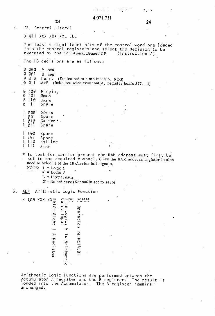


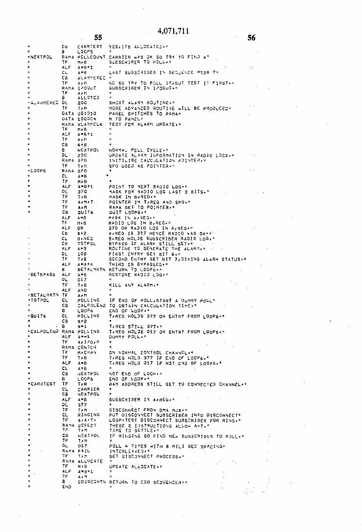


![United States Patent 4,731,05 1 WI - NASA States Patent [191 [ill Patent Number: 4,731,05 1 Fischell [45] Date of Patent: Mar. 15, 1988 ... Zitterkopf, APL Technical Digest.](https://static.fdocuments.us/doc/165x107/5af1f3817f8b9a572b916b5a/united-states-patent-473105-1-wi-nasa-states-patent-191-ill-patent-number.jpg)


![(3.6 e4 · I11111 11111111 Ill 111ll11111111111111111111111ll1111111111111111111 IIIII 1111 United States Patent [191 US0054165 8 8A [ii] Patent Number: 5,416,588](https://static.fdocuments.us/doc/165x107/5c6a976009d3f25e418cb5d8/36-e4-i11111-11111111-ill-111ll11111111111111111111111ll1111111111111111111.jpg)
![United States Patent pi] - NASA · 2013-04-10 · United States Patent US005429997A [191 pi] Patent Number: 5,429,997 - 1 I I ... Material Science and Technology Division Eng. A155,](https://static.fdocuments.us/doc/165x107/5edb55c2ad6a402d666580c7/united-states-patent-pi-nasa-2013-04-10-united-states-patent-us005429997a-191.jpg)
![United States Patent Patent Number: 4,726,069 Date of · United States Patent [191 Stevenson [11] ... modulation and signal processing for single sideband communications systems which](https://static.fdocuments.us/doc/165x107/5af92c7c7f8b9a32348c0d1b/united-states-patent-patent-number-4726069-date-of-states-patent-191-stevenson.jpg)

![United States Patent [191 [11] Patent Number: 5,389,382 [45] Date … · 2017. 4. 6. · United States Patent [191 List et a1. USOO5389382A [11] Patent Number: [45] Date of Patent:](https://static.fdocuments.us/doc/165x107/60bd3e45b423d52f4d291c3d/united-states-patent-191-11-patent-number-5389382-45-date-2017-4-6.jpg)


![United Q States Patent [191 [11] 4,160,479](https://static.fdocuments.us/doc/165x107/61fb4e9e2e268c58cd5c9e13/united-q-states-patent-191-11-4160479.jpg)