
THE INFLUENCE OF MICROWAVE DRYING ON PHYSICOCHEMICAL PROPERTIES OF

UNIT I MICROWAVE NETWORK THEORY
Introduction –Microwave frequency range, applications of microwaves– Scattering matrixrepresentation of multi port network properties of S-parameters – S matrix of a two port network with mismatched load – Z and ABCD parameters-Comparison between [S] - [Z] and [Y] matrices

Electromagnetic spectrum

Microwaves
Microwaves are electromagnetic waves whose frequencies range from about 300 MHz – 300 GHz (1 MHz = 10 6 Hz and 1 GHz = 10 9 Hz) or wavelengths in air ranging from 100 cm – 1 mm.
The word Microwave means very short wave, which is the shortest wavelength region of the radio spectrum and a part of the electromagnetic spectrum.
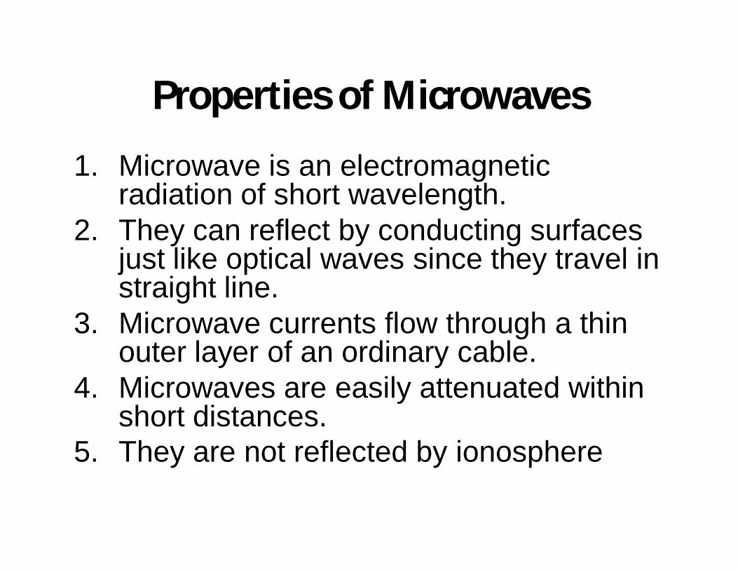
Properties of Microwaves
1. Microwave is an electromagnetic radiation of short wavelength.
2. They can reflect by conducting surfaces just like optical waves since they travel in straight line.
3. Microwave currents flow through a thin outer layer of an ordinary cable.
4. Microwaves are easily attenuated within short distances.
5. They are not reflected by ionosphere
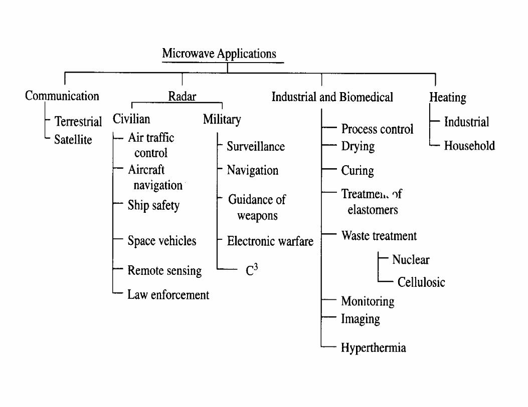

Applications
Microwaves have a wide range of applications in modern technology, which are listed below
1. Telecommunication: Intercontinental Telephone and TV, space communication (Earth – to – space and space – to – Earth), telemetry communication link for railways etc.
2. Radars: detect aircraft, track / guide supersonic missiles, observe and track weather patterns, air traffic control (ATC), burglar alarms, garage door openers, police speed detectors etc.

Commercial and industrial applications
Microwave oven Drying machines – textile, food and paper industry for drying
clothes, potato chips, printed matters etc. Food process industry – Precooling / cooking, pasteurization /
sterility, hat frozen / refrigerated precooled meats, roasting of food grains / beans.
Rubber industry / plastics / chemical / forest product industries Mining / public works, breaking rocks, tunnel boring, drying /
breaking up concrete, breaking up coal seams, curing of cement.
Drying inks / drying textiles, drying / sterilizing grains, drying / sterilizing pharmaceuticals, leather, tobacco, power transmission.
Biomedical Applications ( diagnostic / therapeutic ) –diathermy for localized superficial heating, deep electromagnetic heating for treatment of cancer, hyperthermia ( local, regional or whole body for cancer therapy).

THE SCATTERING MATRIX• Usually we use Y, Z, H or ABCD parameters to describe a linear
two port network.• These parameters require us to open or short a network to
find the parameters. • At radio frequencies it is difficult to have a proper short or
open circuit, there are parasitic inductance and capacitance in most instances.
• Open/short condition leads to standing wave, can cause oscillation and destruction of device.
• For non-TEM propagation mode, it is not possible to measure voltage and current. We can only measure power from E and H fields.
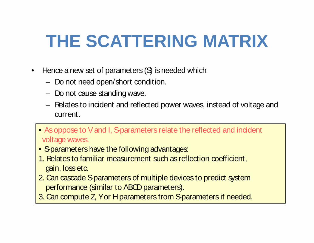
THE SCATTERING MATRIX• Hence a new set of parameters (S) is needed which
– Do not need open/short condition.– Do not cause standing wave.– Relates to incident and reflected power waves, instead of voltage and
current.
• As oppose to V and I, S-parameters relate the reflected and incidentvoltage waves.
• S-parameters have the following advantages:1. Relates to familiar measurement such as reflection coefficient,
gain, loss etc.2. Can cascade S-parameters of multiple devices to predict system
performance (similar to ABCD parameters).3. Can compute Z, Y or H parameters from S-parameters if needed.

THE SCATTERING MATRIX Consider an n – port network:
Each port is considered to beconnected to a Tline withspecific Zc.
Linear n - portnetwork
T-line orwaveguide
Port 2
Port 1
Port n
Reference planefor local z-axis(z = 0)
Zc2
Zc1
Zcn

THE SCATTERING MATRIX• There is a voltage and current on each port.• This voltage (or current) can be decomposed into the incident (+) and reflected component (-).
V1+ V1
-
Linear n - portNetwork
Port 2
Port 1
Port n
z = 0
V1
I1
+z
Port 1
111 VVV
V1
V1+
+
- V1-
+
1111
111
VV
III
cZ
222
22
0 VVVV
eVeVzV zjzj
222
22
0 IIII
eIeIzI zjzj
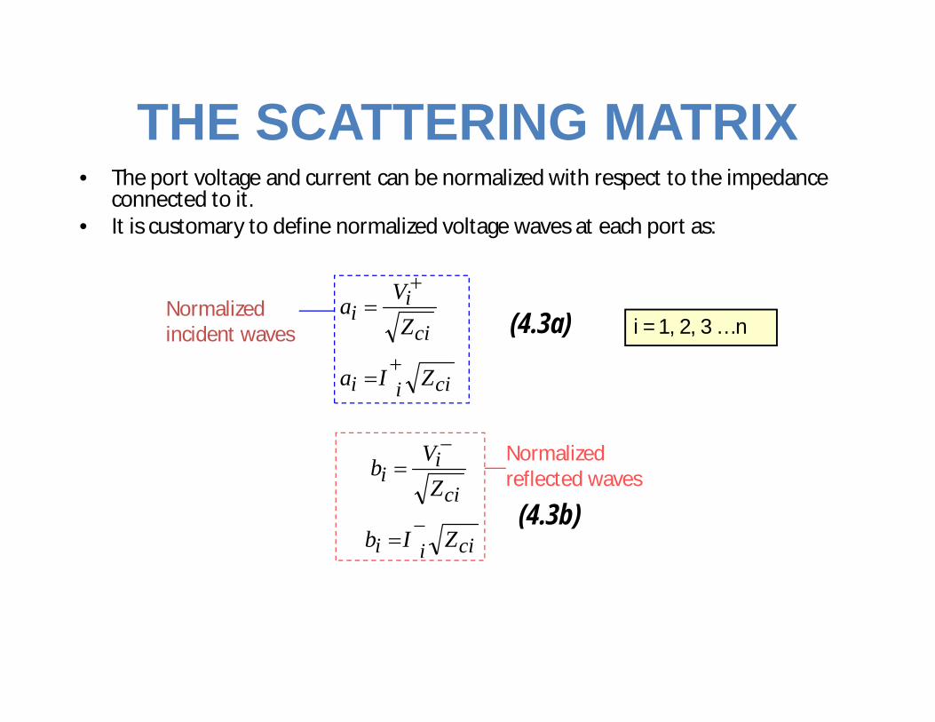
THE SCATTERING MATRIX• The port voltage and current can be normalized with respect to the impedance
connected to it.• It is customary to define normalized voltage waves at each port as:
ciii
ci
ii
ZIa
ZVa
(4.3a)Normalizedincident waves
Normalizedreflected waves
ciii
ci
ii
ZIb
ZVb
(4.3b)
i = 1, 2, 3 … n

THE SCATTERING MATRIX• Thus in general:
Vi+ and Vi
- are propagatingvoltage waves, which canbe the actual voltage for TEMmodes or the equivalent voltages for non-TEM modes.(for non-TEM, V is definedproportional to transverse Efield while I is defined propor-tional to transverse H field, see[1] for details).
V2+
V2-
V1+ V1
-
Vn+
Vn-
Linear n - portNetwork
T-line orwaveguide
Port 2
Port 1
Port nZc1
Zc2
Zcn

THE SCATTERING MATRIX• If the n – port network is linear (make sure you know what this means!), there is a linear relationship
between the normalized waves.• For instance if we energize port 2:
V2+
V1-
Vn-
Port 2
Port 1
Port nZc1
Zc2
Zcn
V2-
Linear n - portNetwork
Constant thatdepends on the network construction
2222
VsV
22
VsVnn
2121
VsV

THE SCATTERING MATRIX• Considering that we can send energy into all ports, this can be
generalized to:
• Or written in Matrix equation:
• Where sij is known as the generalized Scattering (S) parameter, or just S-parameters for short. From (4.3), each port i can have different characteristic impedance Zci
nnnnnnn
VsVsVsVsV 332211
(4.4a)
(4.4b)or
nn
VsVsVsVsV13132121111
nnVsVsVsVsV
23232221212
VSV
nnnnn
n
n
nV
VV
sss
ssssss
V
VV
:...
:::......
:2
1
21
22221
11211
2
1

THE SCATTERING MATRIX• Consider the N-port network shown in figure 4.1.
Figure 4.1: An arbitrary N-port microwave network
THE SCATTERING MATRIX
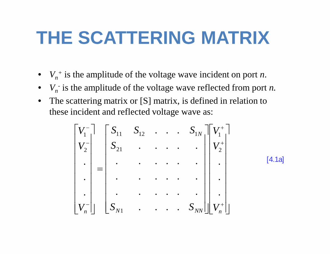
• Vn+ is the amplitude of the voltage wave incident on port n.
• Vn- is the amplitude of the voltage wave reflected from port n.
• The scattering matrix or [S] matrix, is defined in relation to these incident and reflected voltage wave as:
nNNN
N
n V
VV
SS
SSSS
V
VV
.
.
.
...........................
...
.
.
.2
1
1
21
11211
2
1
[4.1a]

THE SCATTERING MATRIX VSVor [4.1b]
jkforVj
iij
kVVS
,0
A specific element of the [S] matrix can be determined as:
[4.2]
Sij is found by driving port j with an incident wave Vj+, and measuring
the reflected wave amplitude, Vi-, coming out of port i.
The incident waves on all ports except j-th port are set to zero (which means that all ports should be terminated in matched load to avoid reflections).Thus, Sii is the reflection coefficient seen looking into port i when all other ports are terminated in matched loads, and Sij is the transmission coefficient from port j to port i when all other ports are terminated in matched loads.
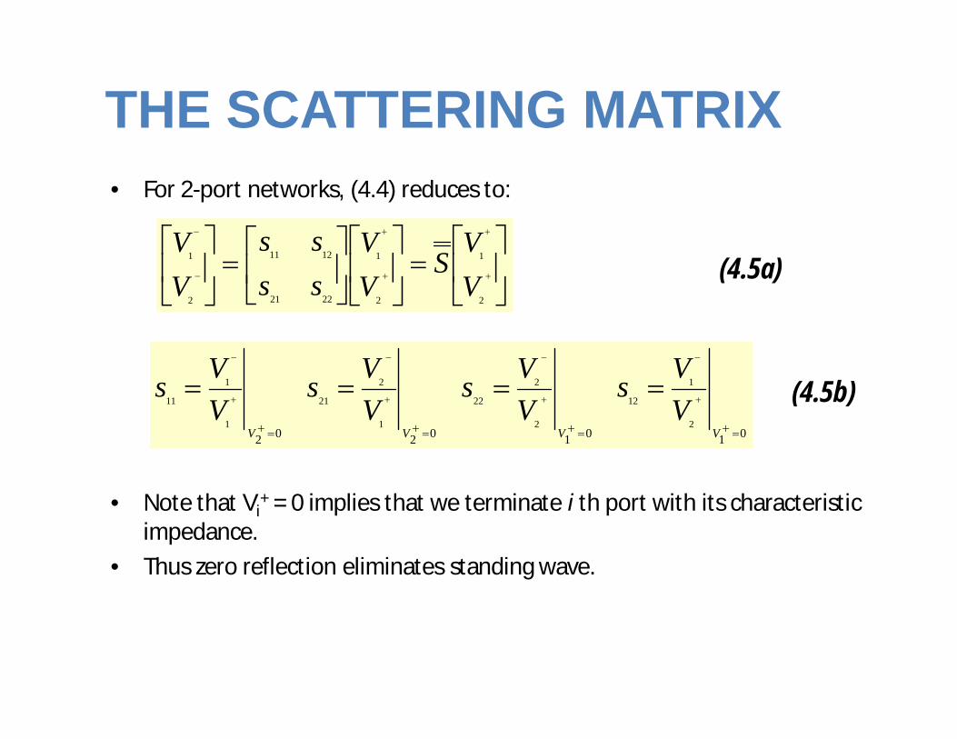
THE SCATTERING MATRIX• For 2-port networks, (4.4) reduces to:
• Note that Vi+ = 0 implies that we terminate i th port with its characteristic
impedance. • Thus zero reflection eliminates standing wave.
2
1
2
1
2221
1211
2
1
VV
SVV
ssss
VV
(4.5a)
(4.5b)01010202
2
1
12
2
2
22
1
2
21
1
1
11
VVVV
VVs
VVs
VVs
VVs

THE SCATTERING MATRIX
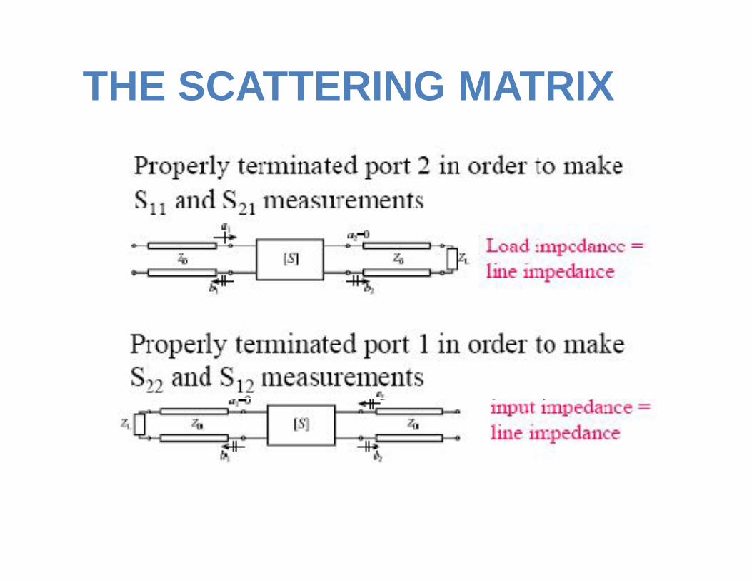
2 – Port Zc2
Zc2Zc1
Zc1Vs
V1+
02021
2
21
1
1
11
VV
VVs
VVs
V1-
V2-
V1-
2 – PortZc1
Zc2Zc1
Zc2 Vs
V2-
V2+
01012
1
12
2
2
22
VV
VVs
VVs
Measurement of s11 and s21:
Measurement of s22 and s12:

THE SCATTERING MATRIX• Input-output behavior of network is defined in terms of normalized
power waves• S-parameters are measured based on properly terminated transmission
lines (and not open/short circuit conditions)
1* }]{[][ tss
THE SCATTERING MATRIX
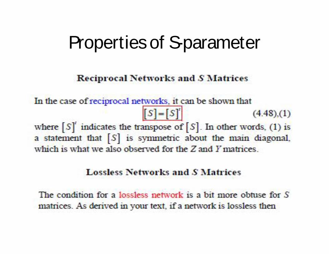
Properties of S-parameter

Properties of S-parameter

Properties of S-parameter

Properties of S-parameter
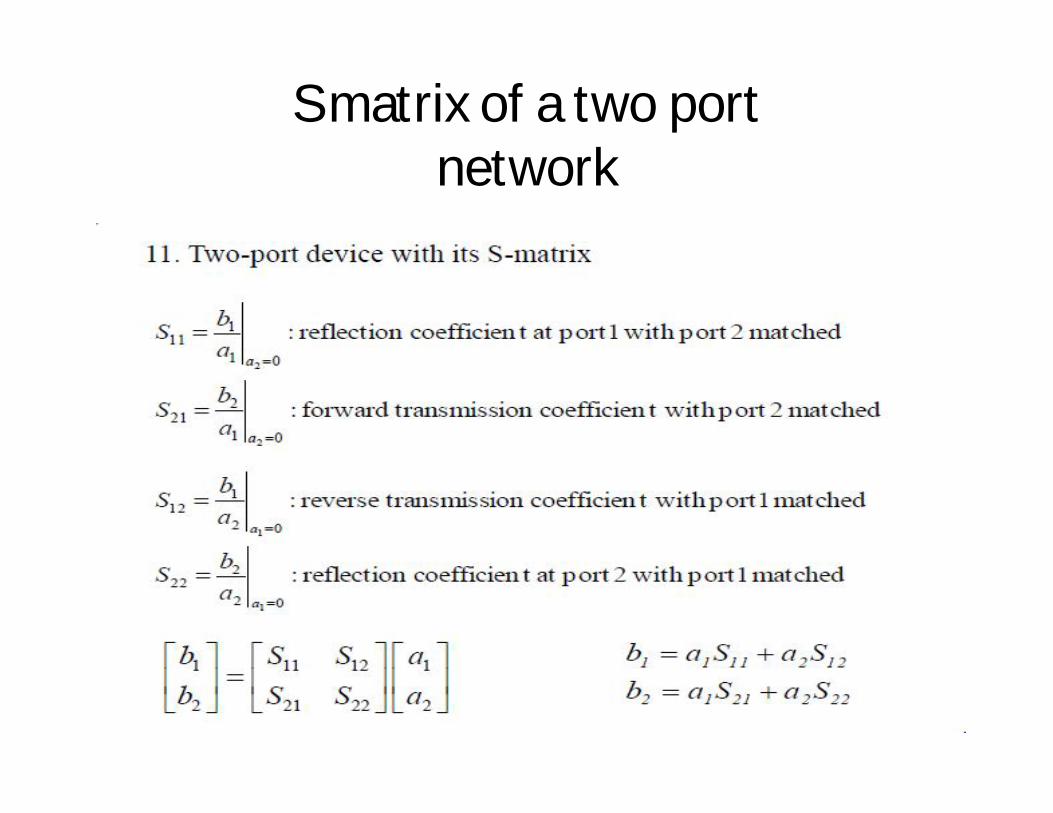
S matrix of a two portnetwork
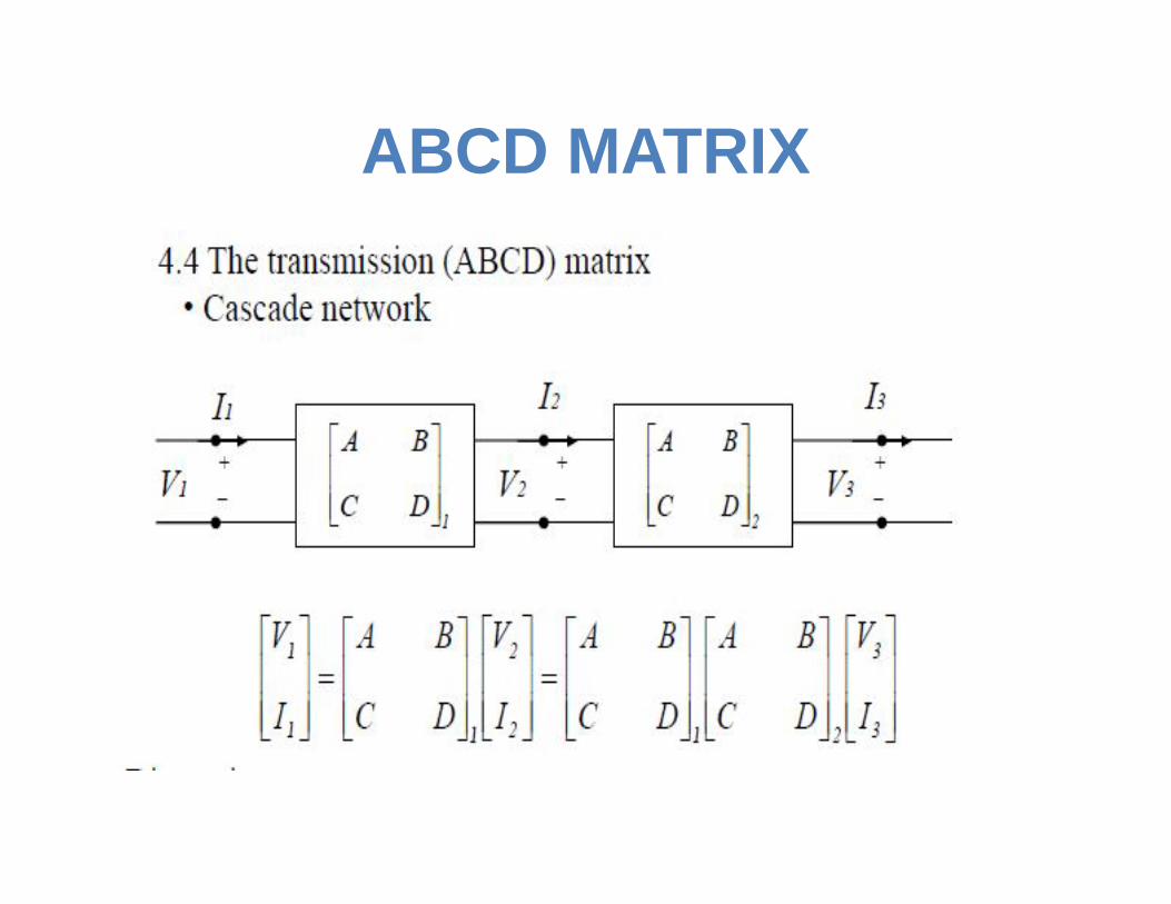
ABCD MATRIX

ABCD MATRIX• The ABCD matrix is useful for characterizing the overall response of 2-port
networks that are cascaded to each other.
3
3
33
33
1
1
3
3
22
22
11
11
1
1
IV
DCBA
IV
IV
DCBA
DCBA
IVI2’
V2V1
I1I2
V3
I3
11
11DCBA
22
22DCBA
Overall ABCD matrix

UNIT II MICROWAVE PASSIVE DEVICES
Coaxial cables-connectors and adapters –Wave guides- Matched terminations –Rectangular to circular wave guide transition–Wave guide corners – Bends and twists –Windows –Attenuators – Phase shifters – Wave guide tees– E plane tee – H plane tee – Magic tee – Isolators – Circulators –Directional couplers –scattering matrix derivation for all components .

Microwave coaxial connectors

Microwave coaxial connectors

Microwave coaxial connectors

Microwave coaxial connectors

Microwave coaxial connectors

Waveguide tees:• Waveguide junctions are used in microwave technologies
when power in a waveguide needs to be split or someextracted.
• There are a number of different types of waveguide junctionthat can be used.
• Each type having different properties - the different types ofwaveguide junction affect the energy contained within thewaveguide in different ways.
• When selecting a waveguide junction balances betweenperformance and cost need to be made and therefore anunderstanding of the different types of waveguide junction isuseful.

Types of Waveguide Tee Junctions:
• There are a number of different types of waveguide junction.The major types are listed below:
1. H-type T Junction2. E-Type T Junction3. Magic T waveguide junction4. Hybrid Ring Waveguide Junction

E-Type Waveguide Junction
• It is called an E-type Tjunction because the junctionarm, i.e. the top of the "T"extends from the mainwaveguide in the samedirection as the E field.
• It is characterized by the factthat the outputs of this formof waveguide junction are180° out of phase with eachother.
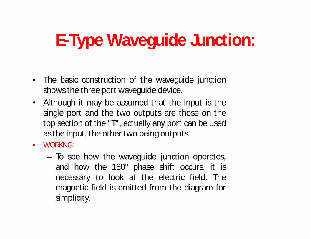
E-Type Waveguide Junction:
• The basic construction of the waveguide junctionshows the three port waveguide device.
• Although it may be assumed that the input is thesingle port and the two outputs are those on thetop section of the "T", actually any port can be usedas the input, the other two being outputs.
• WORKNG:
– To see how the waveguide junction operates,and how the 180° phase shift occurs, it isnecessary to look at the electric field. Themagnetic field is omitted from the diagram forsimplicity.

Working:
• It can be seen from the electric fieldthat when it approaches the Tjunction itself, the electric field linesbecome distorted and bend.
• They split so that the "positive" end ofthe line remains with the top side ofthe right hand section in the diagram,but the "negative“ end of the fieldlines remain with the top side of theleft hand section. In this way thesignals appearing at either section ofthe "T" are out of phase.
• These phase relationships arepreserved if signals enter from eitherof the other ports.

H-type waveguide junction
• This type of waveguide junctionis called an H-type T junctionbecause the long axis of themain top of the "T" arm isparallel to the plane of themagnetic lines of force in thewaveguide.
• It is characterized by the factthat the two outputs from thetop of the "T“ section in thewaveguide are in phase witheach other.
Working:
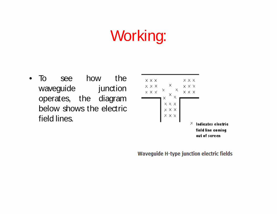
• To see how thewaveguide junctionoperates, the diagrambelow shows the electricfield lines.

Working
• The electric field lines are shown using the traditionalnotation - a cross indicates a line coming out of the screen,whereas a dot indicates an electric field line going into thescreen.
• It can be seen from the diagram that the signals at all portsare in phase.
• Although it is easiest to consider signals entering from thelower section of the "T", any port can actually be used - thephase relationships are preserved whatever entry port isused.

Magic T hybrid waveguide junction
• The magic-T is a combinationof the H-type and E-type Tjunctions. The most commonapplication of this type ofjunction is as the mixersection for microwave radarreceivers.
• The diagram besides givessimplified version of theMagic T waveguide junctionwith its four ports.

Working:

Working:
• E-plane:– To look at the operation of the Magic T
waveguide junction, take the exampleof when a signal is applied into the "Eplane" arm.
– A signal injected into the E-plane portwill also be divided equally betweenports 1 and 2, but will be 180 degreesout of phase.
• H-plane:– A signal injected into the H-plane port
will be divided equally between ports 1and 2, and will be in phase.

Disadvantage:
• One of the disadvantages of the Magic-T waveguide junctionare that reflections arise from the impedance mismatchesthat naturally occur within it.
• These reflections not only give rise to power loss. Thereflections can be reduced by using matching techniques.
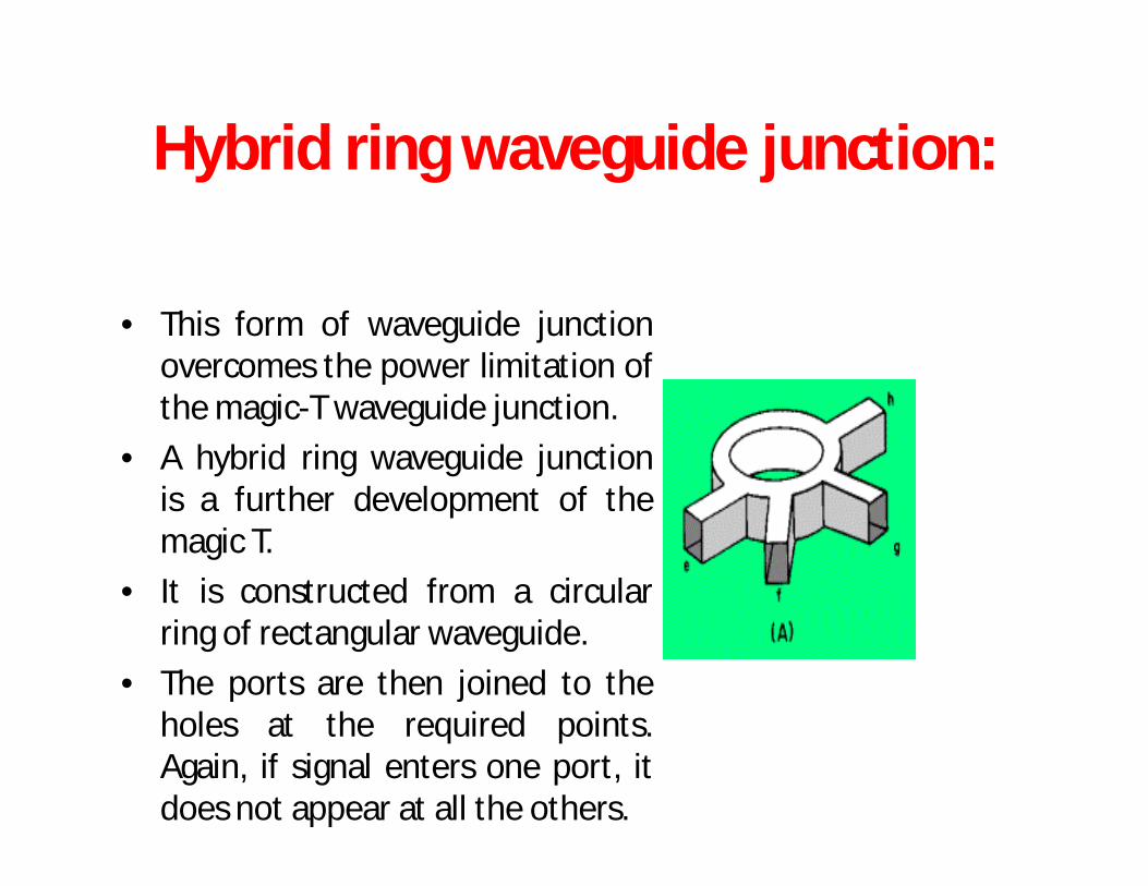
Hybrid ring waveguide junction:
• This form of waveguide junctionovercomes the power limitation ofthe magic-T waveguide junction.
• A hybrid ring waveguide junctionis a further development of themagic T.
• It is constructed from a circularring of rectangular waveguide.
• The ports are then joined to theholes at the required points.Again, if signal enters one port, itdoes not appear at all the others.
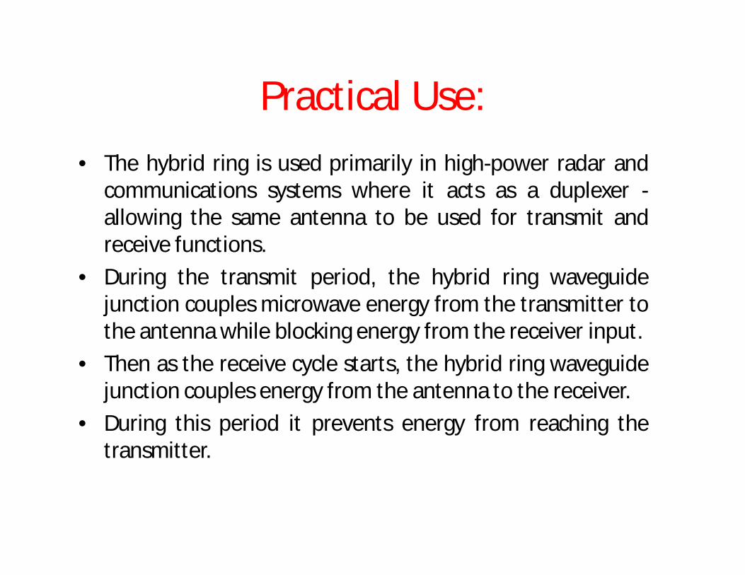
Practical Use:• The hybrid ring is used primarily in high-power radar and
communications systems where it acts as a duplexer -allowing the same antenna to be used for transmit andreceive functions.
• During the transmit period, the hybrid ring waveguidejunction couples microwave energy from the transmitter tothe antenna while blocking energy from the receiver input.
• Then as the receive cycle starts, the hybrid ring waveguidejunction couples energy from the antenna to the receiver.
• During this period it prevents energy from reaching thetransmitter.

Rectangular to circular waveguide transition
Waveguides Bends and Twists
• The size, shape, and dielectric material of a waveguide must be constant throughout its length for energy to move from one end to the other without reflections. Any abrupt change in its size or shape can cause reflections and a loss in overall efficiency. When such a change is necessary, the bends, twists, and joints of the waveguides must meet certain conditions to prevent reflections.
• Bends• Waveguides may be bent in several ways that do not cause
reflections. One way is the gradual bend shown in the right part of the following figure. This gradual bend is known as an E bend because it distorts the E fields. The E bend must have a radius greater than two wavelengths to prevent reflections.
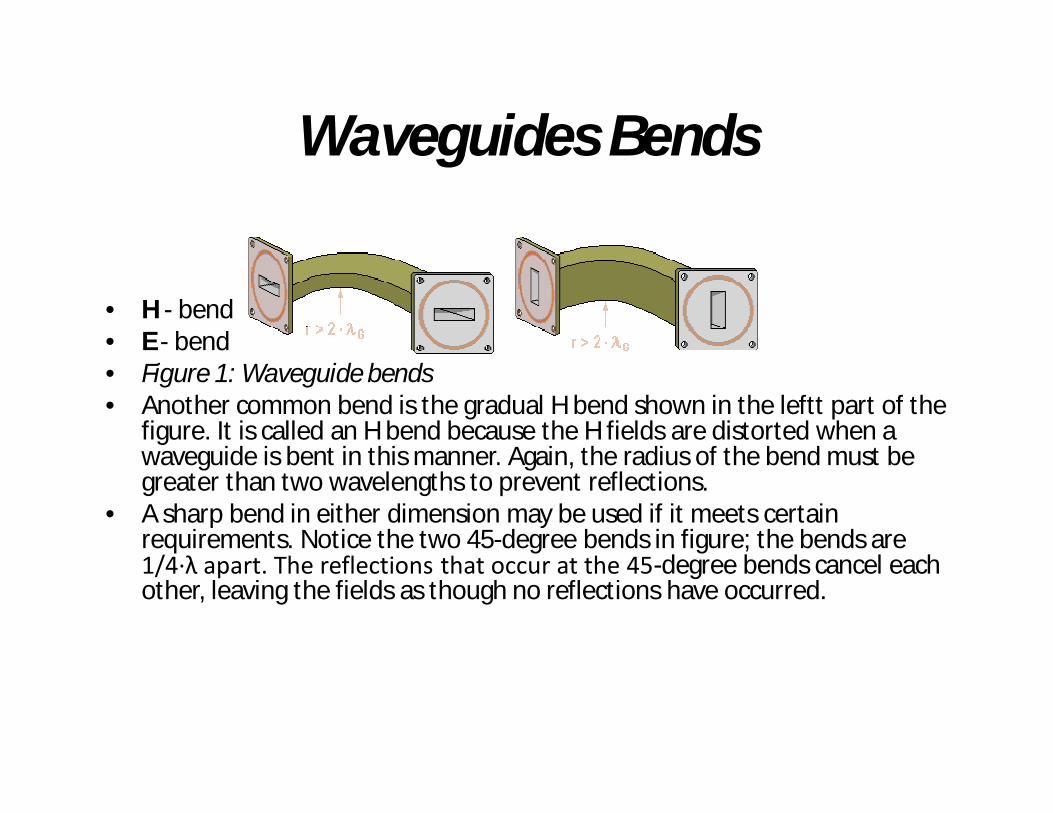
Waveguides Bends
• H - bend• E - bend• Figure 1: Waveguide bends• Another common bend is the gradual H bend shown in the leftt part of the
figure. It is called an H bend because the H fields are distorted when a waveguide is bent in this manner. Again, the radius of the bend must be greater than two wavelengths to prevent reflections.
• A sharp bend in either dimension may be used if it meets certain requirements. Notice the two 45-degree bends in figure; the bends are 1/4·λ apart. The reflections that occur at the 45-degree bends cancel each other, leaving the fields as though no reflections have occurred.
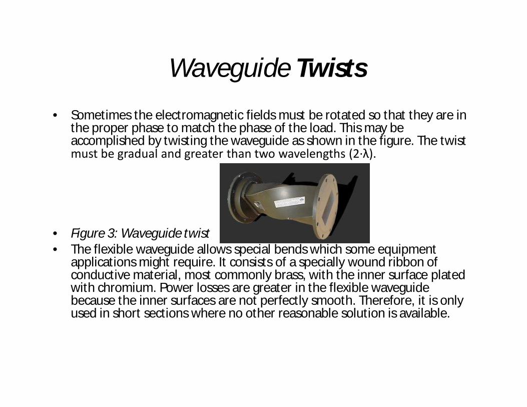
Waveguide Twists
• Sometimes the electromagnetic fields must be rotated so that they are in the proper phase to match the phase of the load. This may be accomplished by twisting the waveguide as shown in the figure. The twist must be gradual and greater than two wavelengths (2·λ).
• Figure 3: Waveguide twist• The flexible waveguide allows special bends which some equipment
applications might require. It consists of a specially wound ribbon of conductive material, most commonly brass, with the inner surface plated with chromium. Power losses are greater in the flexible waveguide because the inner surfaces are not perfectly smooth. Therefore, it is only used in short sections where no other reasonable solution is available.

Phase shifters
Isolator

Isolator

circulator

Circulator
Circulator
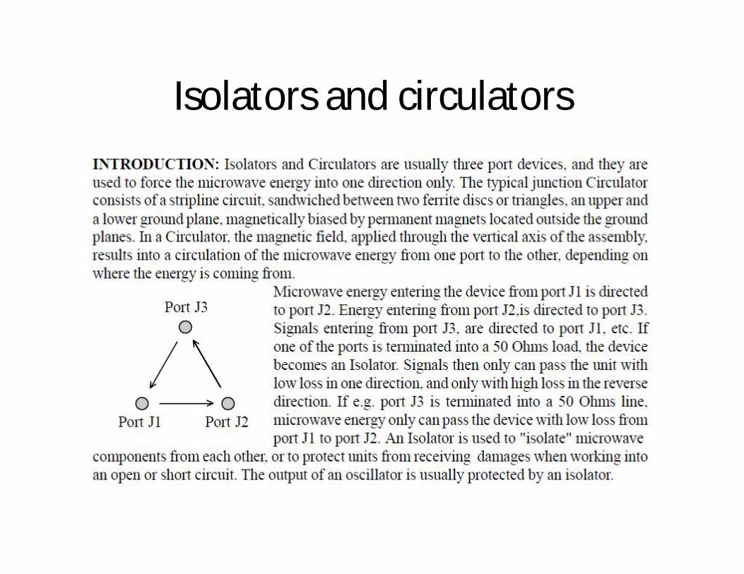
Isolators and circulators
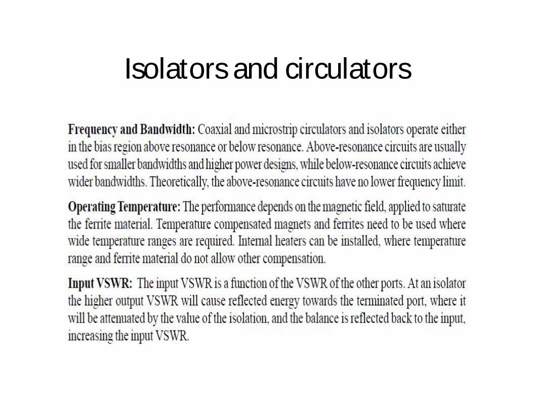
Isolators and circulators
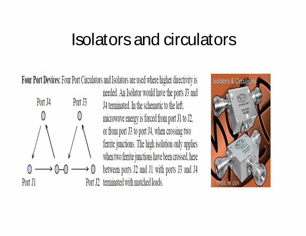
Isolators and circulators
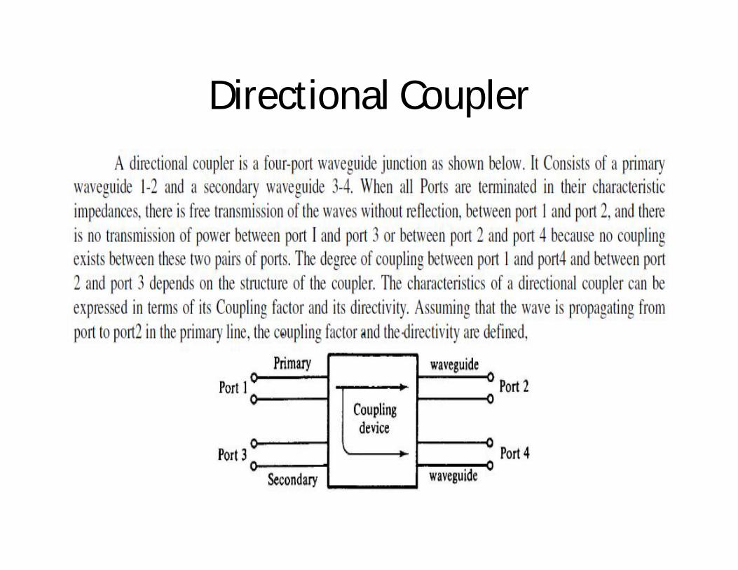
Directional Coupler

Directional Coupler

Directional Coupler

Directional Coupler

Directional Coupler
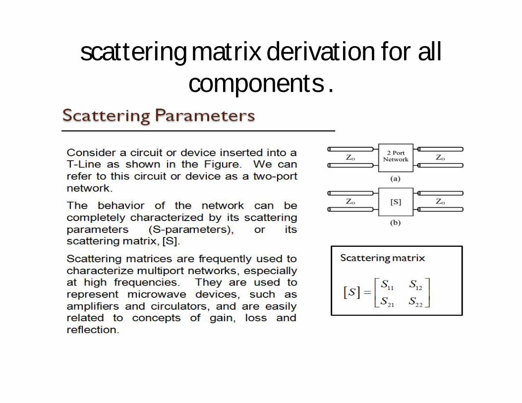
scattering matrix derivation for all components .

scattering matrix derivation for all components .

UNIT III MICROWAVE VACCUM TUBE DEVICES
Introduction – Two cavity klystron amplifier –Mechanism and mode of operation –Power output and efficiency -Applications – Reflex klystron oscillator – Mechanism and mode of operation-Power output – Efficiency – Mode curve –Applications – TWT amplifier – Principle of operation-gain and applications – Magnetron oscillator – Hull cut-off voltage mechanism of operation– Power output and efficiency –Applications – Numerical problems.


Types of Microwave Tubes
Linear beam tubes (O – Type)
Crossed Field Tubes(M – Type)
Eg:KlystronReflex klystronTWT
Eg: Magnetron

Linear beam devices Crossed field devices
(I) Straight path taken bythe electron beam
A principle feature ofsuch tubes is thatelectrons travel in acurved path
(i) DC magnetic field isin parallel with DCelectric field to focus theelectron beam
DC magnetic field isperpendicular to DCelectric field
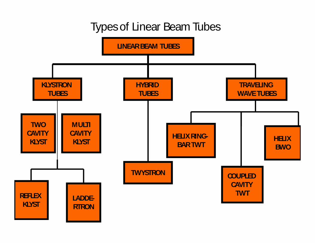
Types of Linear Beam Tubes
TWYSTRON
MULTICAVITY KLYST
TWOCAVITY KLYST
LINEAR BEAM TUBES
KLYSTRON TUBES
HYBRID TUBES
TRAVELING WAVE TUBES
REFLEX KLYST
LADDE-RTRON
HELIX RING-BAR TWT
COUPLED CAVITY
TWT
HELIX BWO

TWYSTRON
• KLYSTRON + TWT = TWYSTRON
• It is hybrid amplifier that uses thecombinations of klystron and TWTcomponents
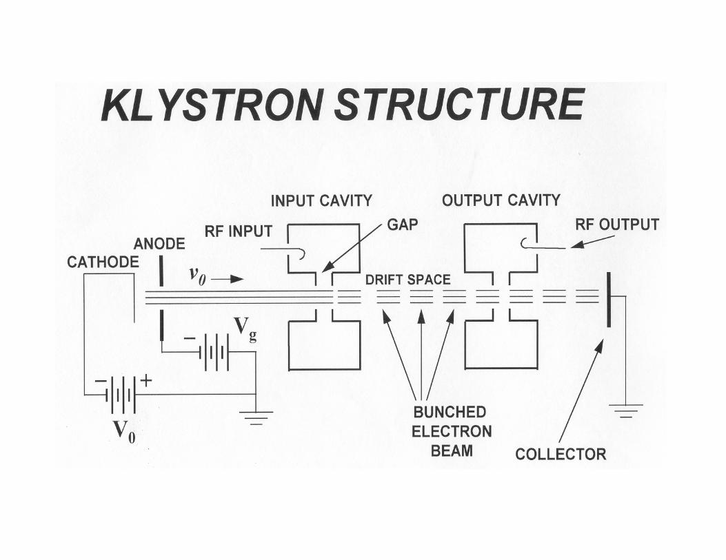

Klystron
• Used in high-power amplifiers• Electron beam moves down tube past several
cavities.• Input cavity is the buncher, output cavity is
the catcher.• Buncher modulates the velocity of the
electron beam


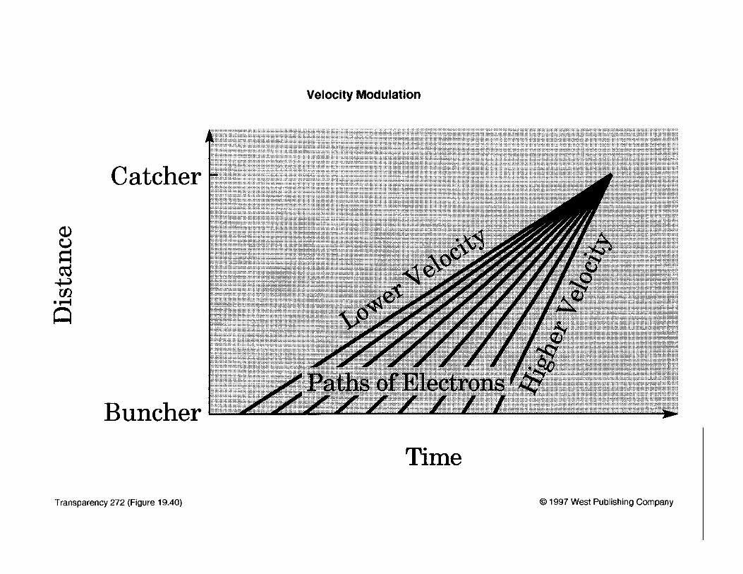
Velocity Modulation
PRINCIPLE
• Electric field from microwaves at buncher alternately speeds and slows electron beam .
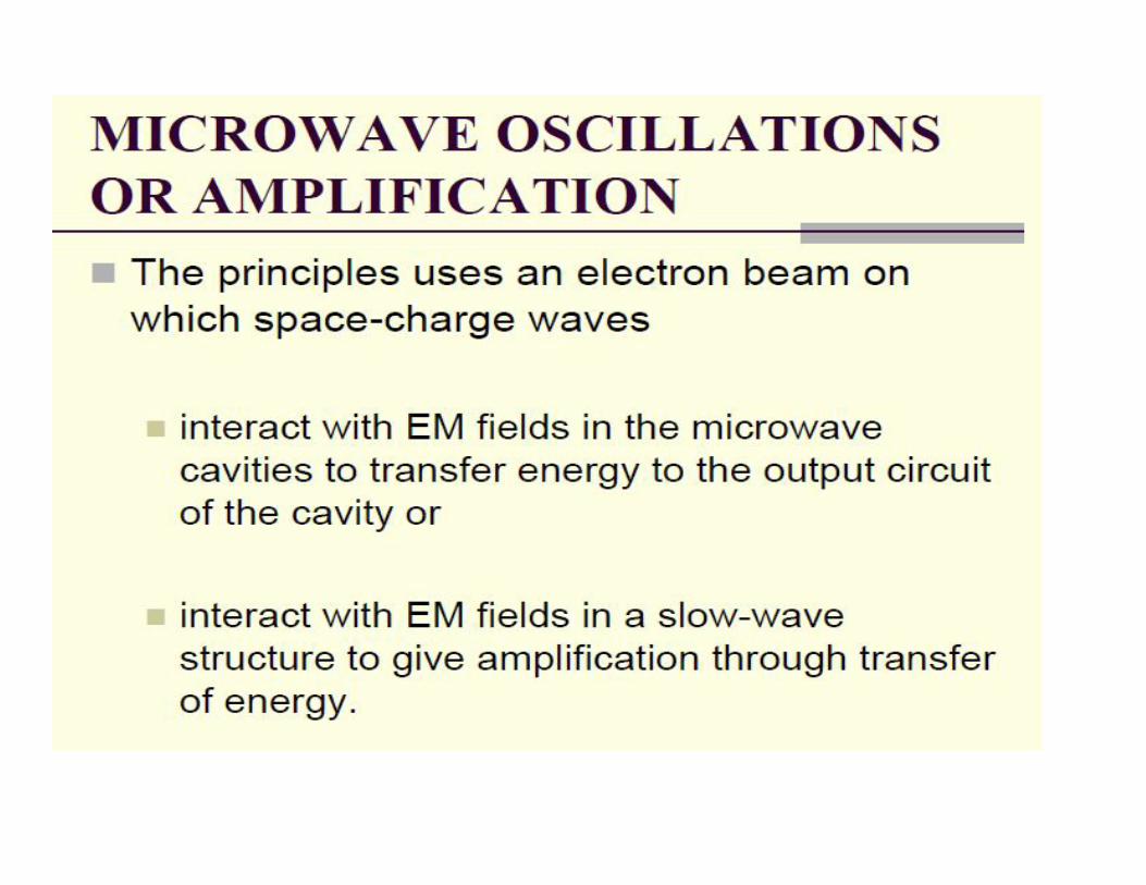
• This causes electrons to bunch up Electron bunches at catcher induce microwaves with more energy.
• The cavities form a slow-wave structure

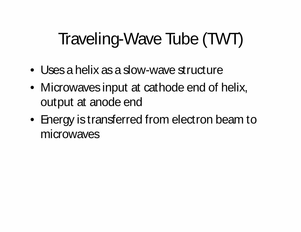
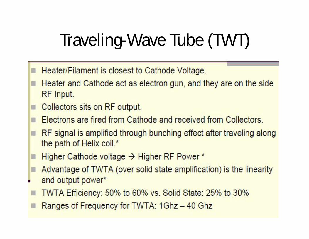
Traveling-Wave Tube (TWT)
• Uses a helix as a slow-wave structure• Microwaves input at cathode end of helix,
output at anode end• Energy is transferred from electron beam to
microwaves
Traveling-Wave Tube (TWT)


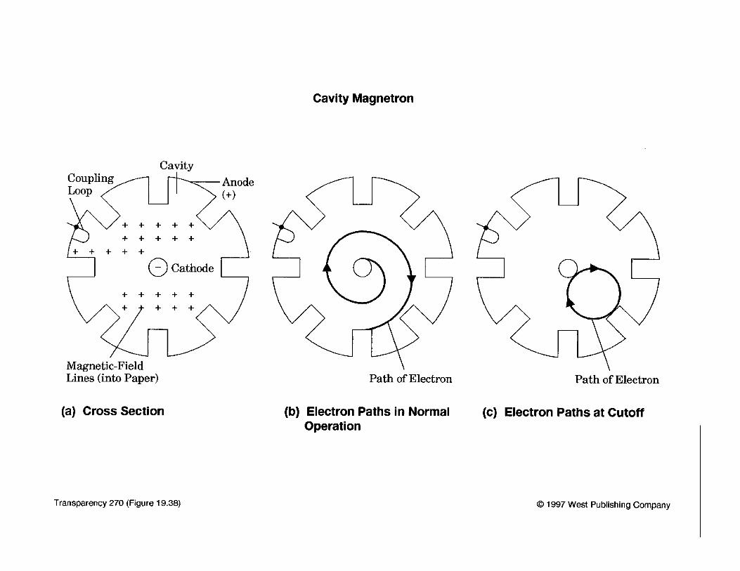
Magnetron Oscillator


UNIT IV MICROWAVE SEMICONDUCTOR DEVICES AND
CIRCUITS Principles of tunnel diodes - Varactor and
Step recovery diodes – Transferred Electron Devices -Gunn diode- Avalanche Transit time devices- IMPATT and TRAPATT Devices-Parametric Amplifiers – Introduction to Micro strip Lines, & Monolithic Microwave Integrated circuits-Materials, MMIC Fabrication Techniques.

Tunnel Diode• It is used as high speed switch, of order nano-seconds. Due to
tunneling effect it has very fast operation in microwave frequency region. It is a two terminal device in which concentration of dopantsis too high.
• The transient response is being limited by junction capacitance plus stray wiring capacitance. Mostly used in microwave oscillators and amplifiers. It acts as most negative conductance device. Tunnel diodes can be tuned in both mechanically and electrically. The symbol of tunnel diode is as shown below.
Tunnel Diode Applications• Oscillatory circuits.• Microwave circuits.• Resistant to nuclear radiation.

Varactor Diode
• These are also known as Varicap diodes. It acts like the variable capacitor. Operations are performed mainly at reverse bias state only. These diodes are very famous due to its capability of changing the capacitance ranges within the circuit in the presence of constant voltage flow.
• They can able to vary capacitance up to high values. In varactor diode by changing the reverse bias voltage we can decrease or increase the depletion layer. These diodes have many applications as voltage controlled oscillator for cell phones, satellite pre-filters etc. The symbol of varactordiode is given below.
Varactor Diode Applications• Voltage-controlled capacitors.• Voltage-controlled oscillators.• Parametric amplifiers.• Frequency multipliers.• FM transmitters and Phase locked loops in radio, television sets and
cellular telephone.

Step Recovery Diodes
• It is also called as snap-off diode or charge-storage diode. These are the special type of diodes which stores the charge from positive pulse and uses in the negative pulse of the sinusoidal signals. The rise time of the current pulse is equal to the snap time. Due to this phenomenon it has speed recovery pulses.
• The applications of these diodes are in higher order multipliers and in pulse shaper circuits. The cut-off frequency of these diodes is very high which are nearly at Giga hertz order.
• As multiplier this diode has the cut-off frequency range of 200 to 300 GHz. In the operations which are performing at 10 GHz range these diodes plays a vital role. The efficiency is high for lower order multipliers. The symbol for this diode is as shown below.

Transferred Electron Devices
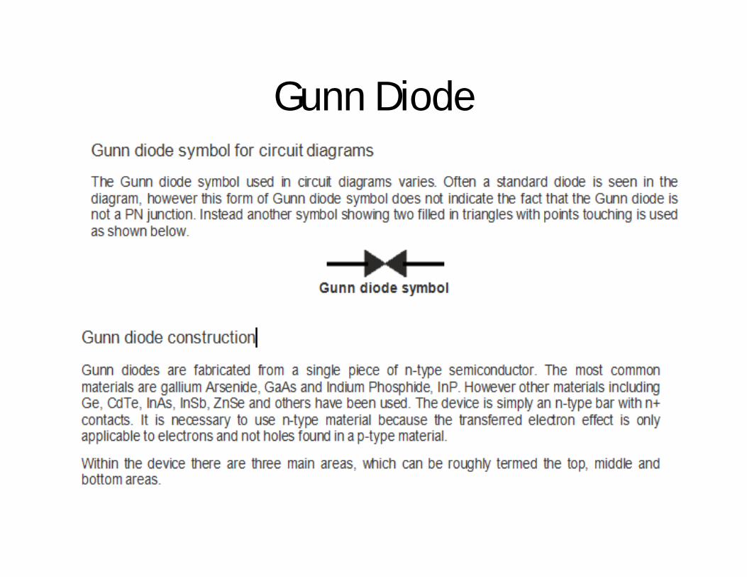
Gunn Diode

Gunn Diode

Avalanche transit time devices
• The process of having a delay between voltage and current, in avalanche together with transit time, through the material is said to be Negative resistance. The devices that helps to make a diode exhibit this property are called as Avalanche transit time devices.
• The examples of the devices that come under this category are IMPATT, TRAPATT and BARITT diodes. Let us take a look at each of them, in detail.
IMPATT Diode
• This is a high-power semiconductor diode, used in high frequency microwave applications. The full form IMPATT is IMPact ionization Avalanche Transit Time diode.
• A voltage gradient when applied to the IMPATT diode, results in a high current. A normal diode will eventually breakdown by this. However, IMPATT diode is developed to withstand all this. A high potential gradient is applied to back bias the diode and hence minority carriers flow across the junction.
• Application of a RF AC voltage if superimposed on a high DC voltage, the increased velocity of holes and electrons results in additional holes and electrons by thrashing them out of the crystal structure by Impact ionization. If the original DC field applied was at the threshold of developing this situation, then it leads to the avalanche current multiplication and this process continues. This can be understood by the following figure.

IMPATT Diode
• Due to this effect, the current pulse takes a phase shift of 90°. However, instead of being there, it moves towards cathode due to the reverse bias applied. The time taken for the pulse to reach cathode depends upon the thickness of n+ layer, which is adjusted to make it 90° phase shift. Now, a dynamic RF negative resistance is proved to exist. Hence, IMPATT diode acts both as an oscillator and an amplifier.

IMPATT Diode
The efficiency of IMPATT diode is represented asη=[PacPdc]=VaVd[IaId]η=[PacPdc]=VaVd[IaId]Where,•PacPac = AC power Vd&IdVd&Id = DC voltage & current
•PdcPdc = DC power Va&IaVa&Ia = AC voltage & current
IMPATT DiodeDisadvantages• Following are the disadvantages of IMPATT diode.• It is noisy as avalanche is a noisy process• Tuning range is not as good as in Gunn diodesApplications• Following are the applications of IMPATT diode.• Microwave oscillator• Microwave generators• Modulated output oscillator• Receiver local oscillator• Negative resistance amplifications• Intrusion alarm networks (high Q IMPATT)• Police radar (high Q IMPATT)• Low power microwave transmitter (high Q IMPATT)• FM telecom transmitter (low Q IMPATT)• CW Doppler radar transmitter (low Q IMPATT)

TRAPATT Diode
The full form of TRAPATT diode is TRApped Plasma Avalanche Triggered Transit diode. A microwave generator which operates between hundreds of MHz to GHz. These are high peak power diodes usually n+- p-p+ or p+-n-n+ structures with n-type depletion region, width varying from 2.5 to 1.25 µm. The following figure depicts this.
TRAPATT Diode
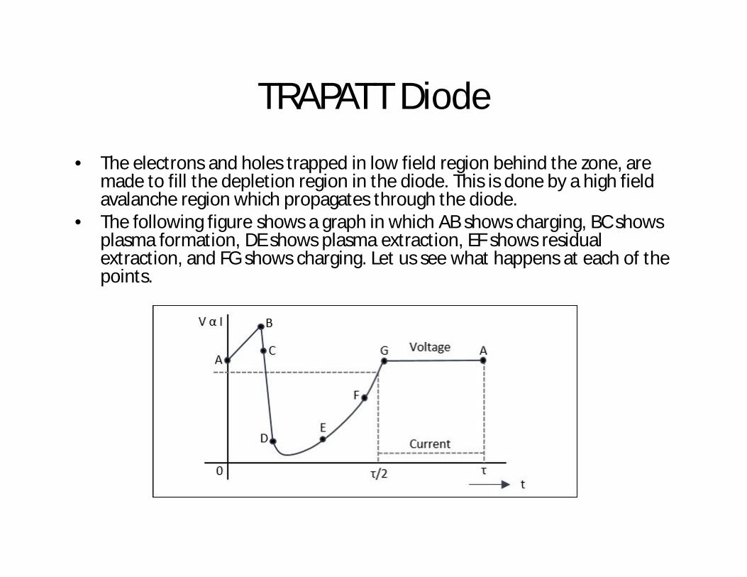
• The electrons and holes trapped in low field region behind the zone, are made to fill the depletion region in the diode. This is done by a high field avalanche region which propagates through the diode.
• The following figure shows a graph in which AB shows charging, BC shows plasma formation, DE shows plasma extraction, EF shows residual extraction, and FG shows charging. Let us see what happens at each of the points.

TRAPATT Diode
• A: The voltage at point A is not sufficient for the avalanche breakdown to occur. At A, charge carriers due to thermal generation results in charging of the diode like a linear capacitance.
• A-B: At this point, the magnitude of the electric field increases. When a sufficient number of carriers are generated, the electric field is depressed throughout the depletion region causing the voltage to decrease from B to C.
• C: This charge helps the avalanche to continue and a dense plasma of electrons and holes is created. The field is further depressed so as not to let the electrons or holes out of the depletion layer, and traps the remaining plasma.
• D: The voltage decreases at point D. A long time is required to clear the plasma as the total plasma charge is large compared to the charge per unit time in the external current.
• E: At point E, the plasma is removed. Residual charges of holes and electrons remain each at one end of the deflection layer.

TRAPATT Diode
• E to F: The voltage increases as the residual charge is removed.• F: At point F, all the charge generated internally is removed.• F to G: The diode charges like a capacitor.• G: At point G, the diode current comes to zero for half a period. The
voltage remains constant as shown in the graph above. This state continues until the current comes back on and the cycle repeats.The avalanche zone velocity VsVs is represented asVs=dxdt=JqNAVs=dxdt=JqNAWhereJJ = Current densityqq = Electron charge 1.6 x 10⁻¹⁹
NANA = Doping concentration
TRAPATT DiodeThe avalanche zone will quickly sweep across most of the diode and the transit time of the carriers is represented asτs=LVsτs=LVsWhereVsVs = Saturated carrier drift velocityLL = Length of the specimenThe transit time calculated here is the time between the injection and the collection. The repeated action increases the output to make it an amplifier, whereas a microwave low pass filter connected in shunt with the circuit can make it work as an oscillator.Applications
• There are many applications of this diode.• Low power Doppler radars• Local oscillator for radars• Microwave beacon landing system• Radio altimeter• Phased array radar, etc.
Parametric Amplifier

Parametric Amplifier

Microstrip lines

Microstrip lines

Microstrip lines

Microstrip lines

Monolithic Microwave Integrated Circuit (MMIC)
• Microwave ICs are the best alternative to conventional waveguide or coaxial circuits, as they are low in weight, small in size, highly reliable and reproducible. The basic materials used for monolithic microwave integrated circuits are −
• Substrate material• Conductor material• Dielectric films• Resistive films• These are so chosen to have ideal characteristics and high
efficiency. The substrate on which circuit elements are fabricated is important as the dielectric constant of the material should be high with low dissipation factor, along with other ideal characteristics. The substrate materials used are GaAs, Ferrite/garnet, Aluminum, beryllium, glass and rutile.
Monolithic Microwave Integrated Circuit (MMIC)
• The conductor material is so chosen to have high conductivity, low temperature coefficient of resistance, good adhesion to substrate and etching, etc. Aluminum, copper, gold, and silver are mainly used as conductor materials. The dielectric materials and resistive materials are so chosen to have low loss and good stability.
• Fabrication Technology• In hybrid integrated circuits, the semiconductor devices and passive circuit
elements are formed on a dielectric substrate. The passive circuits are either distributed or lumped elements, or a combination of both.
• Hybrid integrated circuits are of two types.• Hybrid IC• Miniature Hybrid IC• In both the above processes, Hybrid IC uses the distributed circuit elements that
are fabricated on IC using a single layer metallization technique, whereas Miniature hybrid IC uses multi-level elements.
• Most analog circuits use meso-isolation technology to isolate active n-type areas used for FETs and diodes. Planar circuits are fabricated by implanting ions into semi-insulating substrate, and to provide isolation the areas are masked off.

UNIT V MICROWAVE MEASUREMENTS
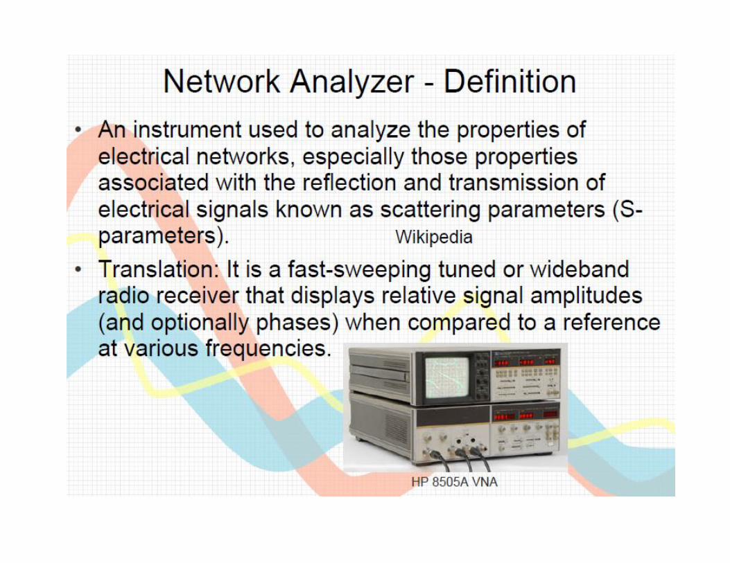
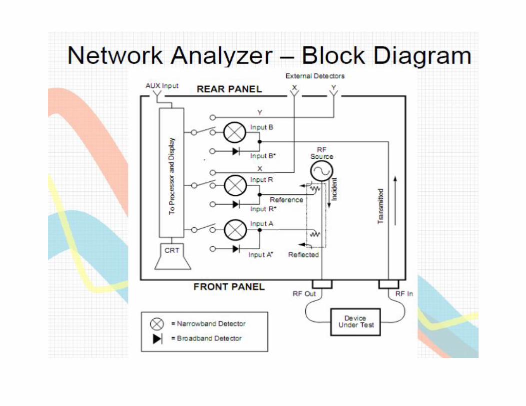
Introduction – Slotted line carriage –– Spectrum analyzer – Network analyzer – Power measurements –Schottky barrier diode sensor –Bolometer sensor –Power sensor – High power measurement – Insertion loss and attenuation measurement – VSWR measurement – Low and high VSWR – Impedance measurement – Frequency measurement –Measurement of cavity Q – Dielectric measurement of a solid by wave-guide method – Antenna measurement – Radiation pattern – Phase and gain.

Slotted Line carriage

Spectrum Analyzer

Spectrum Analyzer

Spectrum Analyzer


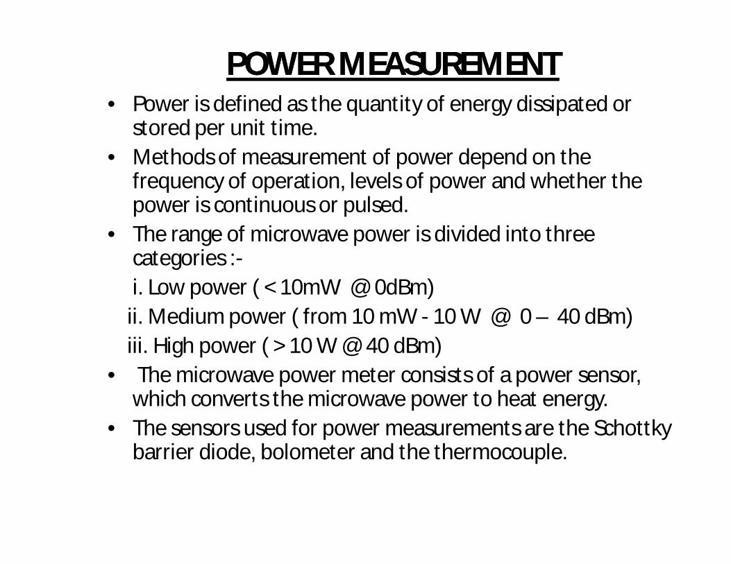
• Power is defined as the quantity of energy dissipated or stored per unit time.
• Methods of measurement of power depend on the frequency of operation, levels of power and whether the power is continuous or pulsed.
• The range of microwave power is divided into three categories :-i. Low power ( < 10mW @ 0dBm)
ii. Medium power ( from 10 mW - 10 W @ 0 – 40 dBm)iii. High power ( > 10 W @ 40 dBm)
• The microwave power meter consists of a power sensor, which converts the microwave power to heat energy.
• The sensors used for power measurements are the Schottky barrier diode, bolometer and the thermocouple.
POWER MEASUREMENTPOWER MEASUREMENT

Power Measurement
• Power may be defined as the rate at which energy is transformed oe made available
• In almost all cases the power in a d.c. circuit is best measured by separately measuring quantities, V and I and by computing P=VI
• In case of a.c. circuits the instantaneous power varies continuously as the current and voltage go through a cycle of values
• The fact that the power factor is involved in the expression for the power means that a wattmeter must be used instead of merely an ammeter and voltmeter.
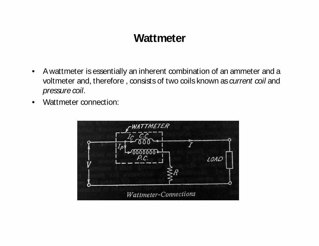
Wattmeter
• A wattmeter is essentially an inherent combination of an ammeter and a voltmeter and, therefore , consists of two coils known as current coil and pressure coil.
• Wattmeter connection:

Measurement of Power in Single Phase A.C. Circuit
• 3-voltmeter method
• Disadvantages : (i) Even small errors in measurement of voltages may cause serious errors in the value of power, (ii) Supply voltage higher than normal voltage is required
RVVV
P2
22
21
23
21
22
21
23
2cos
VVVVV
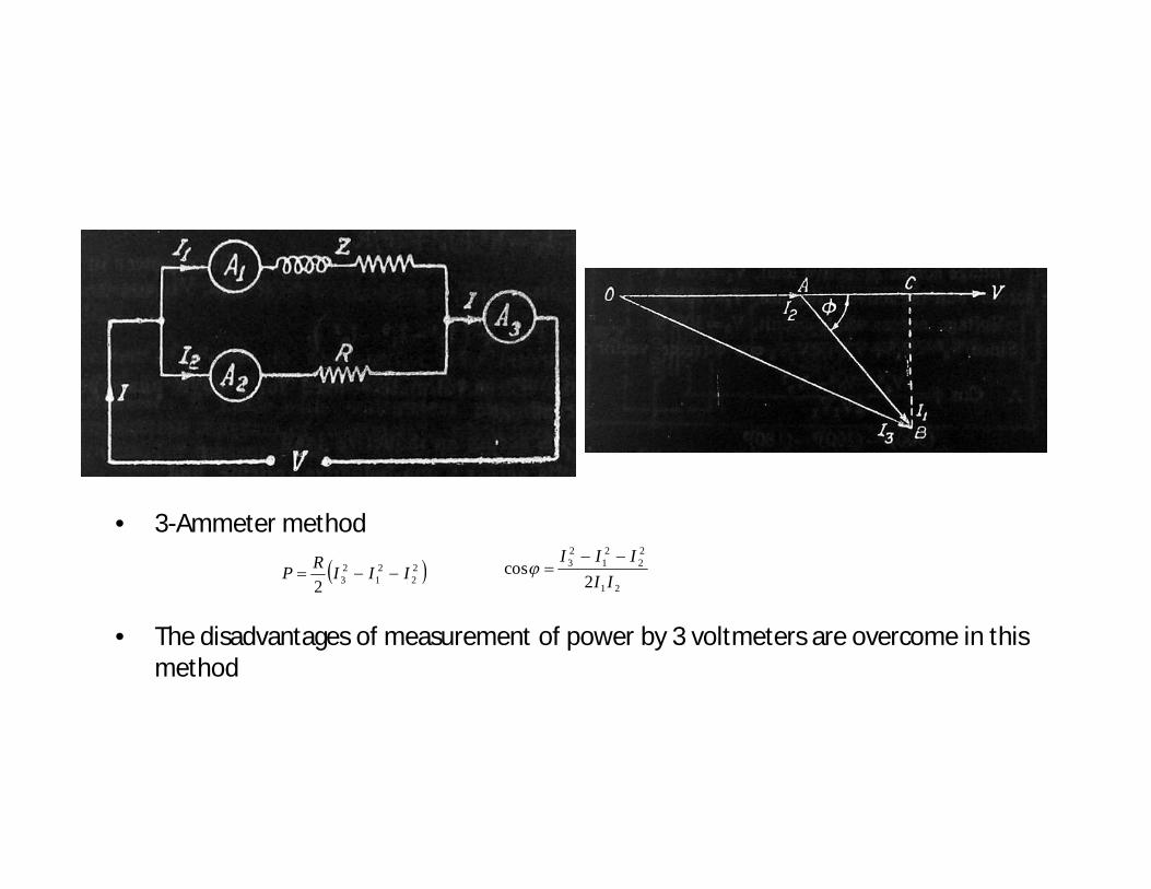
• 3-Ammeter method
• The disadvantages of measurement of power by 3 voltmeters are overcome in this method
22
21
232
IIIRP 21
22
21
23
2cos
IIIII

Measurement of power in conjuction with instrument transformers
• This method is used when the currents and voltages of the circuits to be measured are high
• Figure below shows a measurement of power with wattmeter in conjunction with instrument transformers in single phase A.C. circuits

Measurement of Power in 3-Phase Circuit
• Measurement of power in 3-phase, 4-wire circuits-----------
• P=W1+W2+W3
• Measurement of power in 3-phase, 3-wire circuits-------------
• P=W1+W2+W3

• A zero-biased Schottky Barrier Diode is used as a square-law detector whose output is proportional to the input power.
• The diode detectors can be used to measure power levels as low as 70dBm.
SCHOTTKY BARRIER DIODESCHOTTKY BARRIER DIODE

• A Bolometer is a power sensor whose resistance changes with temperature as it absorbs microwave power.
• Are power detectors that operate on thermal principles. Since the temperature of the resistance is dependent on the signal power absorbed, the resistance must also be in proportion to the signal power.
• The two most common types of bolometer are, the barretter and the thermistor. Both are sensitive power detectors and is used to indicate microwatts of power. They are used with bridge circuits to convert resistance to power using a meter or other indicating devices.
BOLOMETERSBOLOMETERS

BOLOMETERBOLOMETER
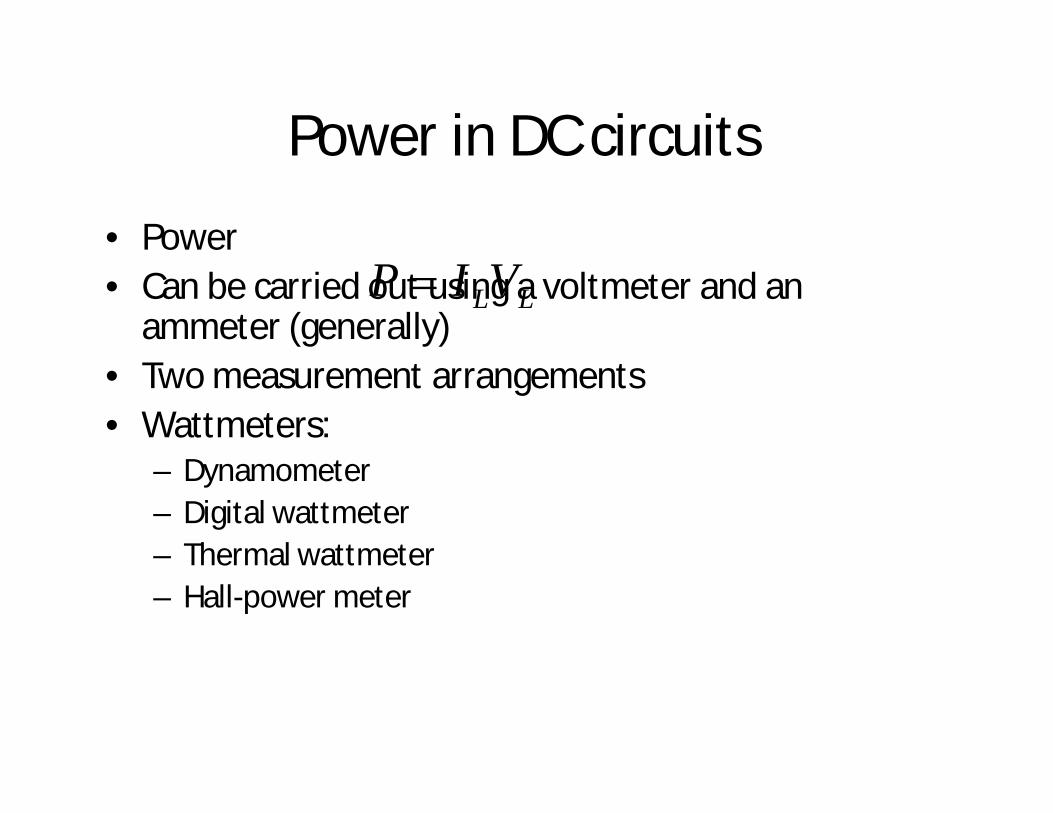
Power in DC circuits
• Power • Can be carried out using a voltmeter and an
ammeter (generally)• Two measurement arrangements• Wattmeters:
– Dynamometer– Digital wattmeter– Thermal wattmeter– Hall-power meter
LLVIP

DC circuits
a) Ammeter measures current which flow into the voltmeter and load
b) Voltmeter measures voltage drop across the ammeter in addition to that dropping across the load
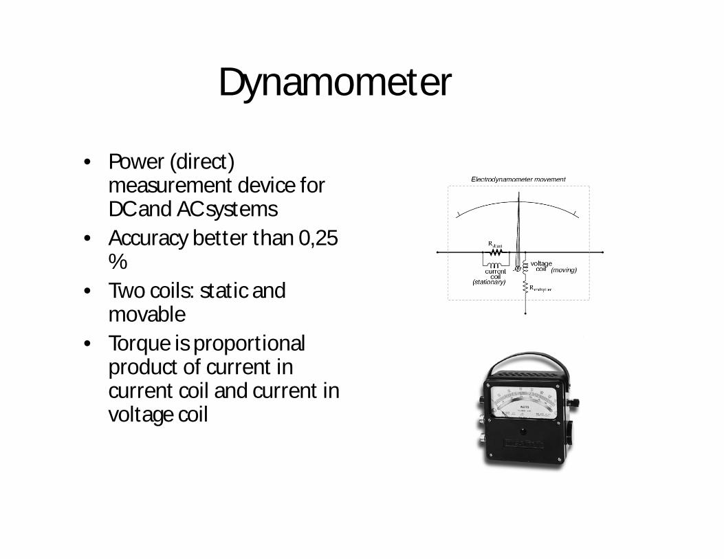
Dynamometer
• Power (direct) measurement device for DC and AC systems
• Accuracy better than 0,25 %
• Two coils: static and movable
• Torque is proportional product of current in current coil and current in voltage coil
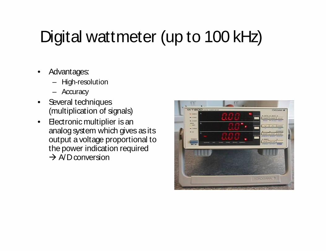
Digital wattmeter (up to 100 kHz)
• Advantages:– High-resolution– Accuracy
• Several techniques (multiplication of signals)
• Electronic multiplier is an analog system which gives as its output a voltage proportional to the power indication required A/D conversion
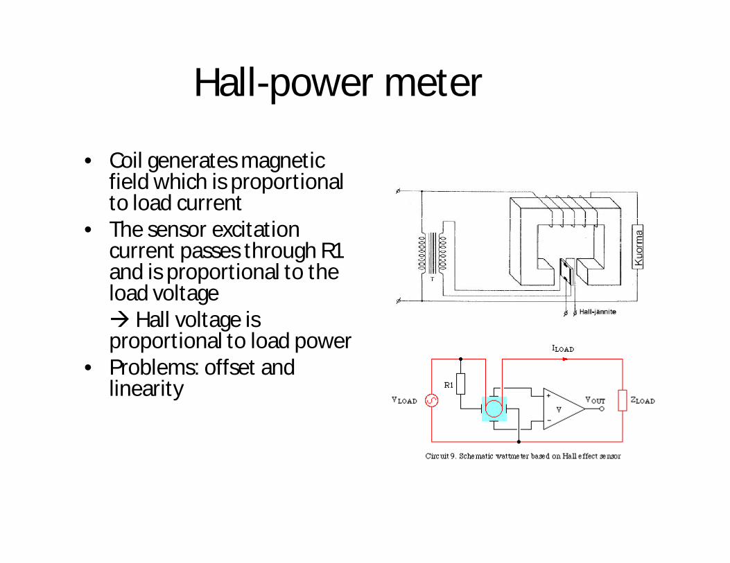
Hall-power meter
• Coil generates magnetic field which is proportional to load current
• The sensor excitation current passes through R1 and is proportional to the load voltage Hall voltage is proportional to load power
• Problems: offset and linearity

Power in AC circuits
• Instantaneous power (time dependence)
• Mean power (usually the most interesting)
• Real power (active work), reactive power, apparent power
• Measures can be done same way as DC circuit (single-phase)
)()()( titvtp
T
dttpT
P0
)(1

AC circuits
cosLLIVP sinLLIVQ 22 QPS
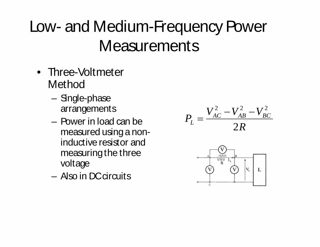
Low- and Medium-Frequency Power Measurements
• Three-Voltmeter Method– Single-phase
arrangements– Power in load can be
measured using a non-inductive resistor and measuring the three voltage
– Also in DC circuits
RVVVP BCABAC
L 2
222

Line-Frequency Power Measurements
• Polyphase Power Measurements– Three-phase systems are most commonly used in
industrial applications– Energy and power generation and distribution– “Real power for consumer”– Reactive power also important (loading) – Power can measured several ways– Power factor

Line-Frequency Power Measurements (2)
• Four (main) different cases which affects to the measurement arrangements:
1. Symmetrical load with neutral conductor2. Symmetrical load without neutral conductor3. Unsymmetrical load with neutral conductor4. Unsymmetrical load without neutral conductor

Insertion Loss
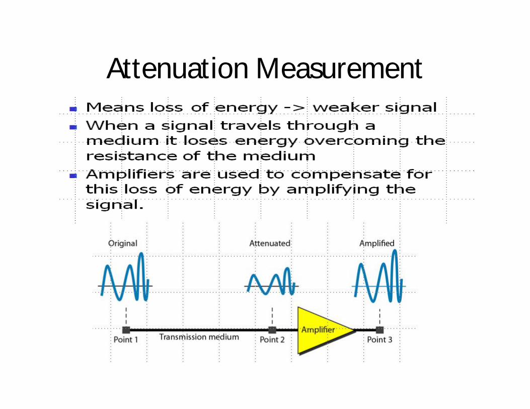
Attenuation Measurement


VSWR Measurement• VSWR is defined as the ratio of the maximum voltage to the minimum
voltage in standing wave pattern along the length of a transmission line structure. It varies from 1 to (plus) infinity and is always positive. Unless you have a piece of slotted line-test equipment this is a hard definition to use, especially since the concept of voltage in a microwave structure has many interpretations.
• Sometimes VSWR is called SWR to avoid using the term voltage and to instead use the concept of power waves. This in turn leads to a mathematical definition of VSWR in terms of a reflection coefficient. A reflection coefficient is defined as the ratio of reflected wave to incident wave at a reference plane. This value varies from -1 (for a shorted load) to +1 (for an open load), and becomes 0 for matched impedance load. It is a complex number. This helps us because we can actually measure power.
•

VSWR Measurement• The reflection coefficient, commonly denoted by the Greek letter gamma (Γ), can be calculated
from the values of the complex load impedance and the transmission line characteristic impedance which in principle could also be a complex number.
• Γ = (Zl - Z0)/(Zl + Z0)• The square of | Γ | is then the power of the reflected wave, the square hinting at a historical
reference to voltage waves.• Now we can define VSWR (SWR) as a scalar value:• VSWR= (1 + | Γ |)/(1 - | Γ |) or in terms of s-parameters: VSWR= (1 + | S11 |)/(1 - | S11 |)• This is fine but what has it to do with common usage in ads and specifications. Generally, VSWR is
sometimes used as a stand-in for a figure of merit for impedance matching. Sometimes this simplification of a scalar quantity and it’s restricted definition can lead to confusion in the matter of a source to load match. Most of the time there is no problem but, technically, VSWR derives from the ratio using the load impedance and the characteristic impedance of the transmission line in which the standing waves reside and not specifically to a source to load match. I prefer to think of VSWR as a figure of merit and to use the reflection coefficient whenever I am trying to solve problems.
• By the way, if you think you have never experienced a standing wave personally, it's very unlikely. Standing waves in a microwave oven are the reason that food is cooked unevenly (the turntable is a partial solution to that problem). The wavelength of the 2.45 GHz signal is about 12 centimeters, or about five inches. Nulls in the radiation (and heating) will be separated at a distance similar to wavelength.
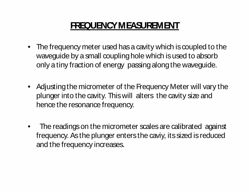
FREQUENCY MEASUREMENTFREQUENCY MEASUREMENT
• The frequency meter used has a cavity which is coupled to the waveguide by a small coupling hole which is used to absorb only a tiny fraction of energy passing along the waveguide.
• Adjusting the micrometer of the Frequency Meter will vary the plunger into the cavity. This will alters the cavity size and hence the resonance frequency.
• The readings on the micrometer scales are calibrated against frequency. As the plunger enters the caviy, its sized is reduced and the frequency increases.
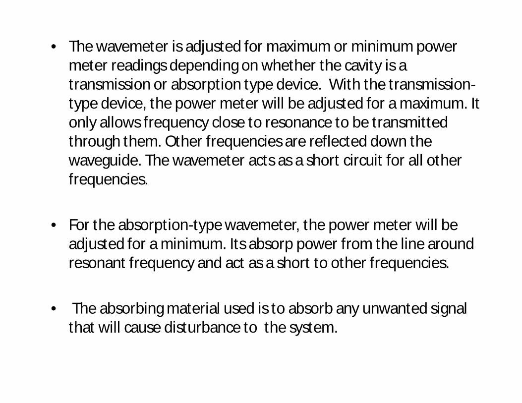
• The wavemeter is adjusted for maximum or minimum power meter readings depending on whether the cavity is a transmission or absorption type device. With the transmission-type device, the power meter will be adjusted for a maximum. It only allows frequency close to resonance to be transmitted through them. Other frequencies are reflected down the waveguide. The wavemeter acts as a short circuit for all other frequencies.
• For the absorption-type wavemeter, the power meter will be adjusted for a minimum. Its absorp power from the line around resonant frequency and act as a short to other frequencies.
• The absorbing material used is to absorb any unwanted signal that will cause disturbance to the system.

VSWR ( VOLTAGE STANDING WAVE RATIO ) VSWR ( VOLTAGE STANDING WAVE RATIO ) MEASUREMENTMEASUREMENT
• Used to determine the degree of mismatch between the source and load when the value VSWR ≠ 1.
• Can be measured by using a slotted line. Direct Method Measurement is used for VSWR values upto about 10. Its value can be read directly using a standing wave detector .
• The measurement consists simply of adjusting attenuator to give an adequate reading, making sure that the frequency is correct and then using the dc voltmeter to measure the detector output at a maximum on the slotted section and then at the nearest minimum.

The ratio of the voltage maximum to the minimum gives the VSWR i.eThe ratio of the voltage maximum to the minimum gives the VSWR i.e
VSWR = VVSWR = Vmaxmax / V/ Vminmin
ISWR = Imax / Imin
= k (V max)2 / k (V min)2
= ( V max / V min)2
= VSWR2
VSWR = √ ( Imax / Imin ) = √ ISWR

• Methods used depends on the value of VSWR whether it is high or low. If the load is not exactly matched to the line, standing wave pattern is produced.
• Reflections can be measured in terms of voltage, current or power. Measurement using voltage is preffered because it is simplicity.
• When reflection occured, the incident and the reflected waves will reinforce each other in some places, and in others they will tend to cancel each other out.
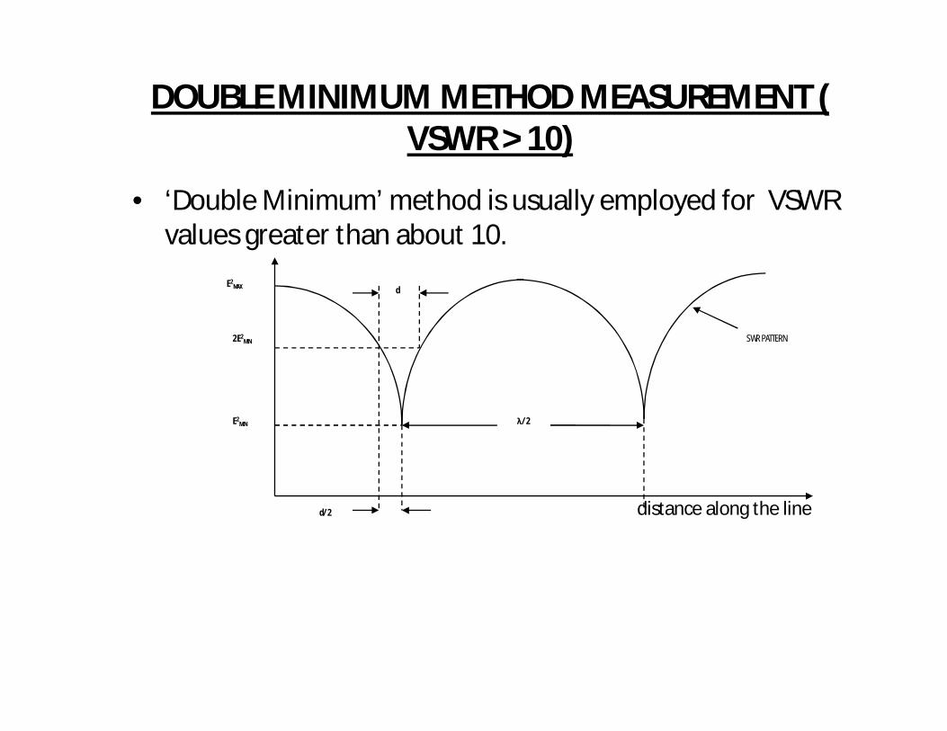
DOUBLE MINIMUM METHOD MEASUREMENT ( VSWR > 10)
• ‘Double Minimum’ method is usually employed for VSWR values greater than about 10.
E2MAX
2E2MIN
E2MIN
d
d/2
λ/2
SWR PATTERN
distance along the line

• The detector output (proportional to field strength squared) is plotted against position. The probe is moved aling the line to find the minimum value of signal.
• It is then moved either side to determine 2 positions at which twice as much detector signal is obtained. The distance d between these two positions then gives the VSWR according to the formula :
S = √ 1 + 1/Sin2(πd/λ)
POWER MEASUREMENTPOWER MEASUREMENT• Power is defined as the quantity of energy dissipated or
stored per unit time. • Methods of measurement of power depend on the
frequency of operation, levels of power and whether the power is continuous or pulsed.
• The range of microwave power is divided into three categories :-i. Low power ( < 10mW @ 0dBm)
ii. Medium power ( from 10 mW - 10 W @ 0 – 40 dBm)iii. High power ( > 10 W @ 40 dBm)
• The microwave power meter consists of a power sensor, which converts the microwave power to heat energy.
• The sensors used for power measurements are the Schottky barrier diode, bolometer and the thermocouple.

SCHOTTKY BARRIER DIODESCHOTTKY BARRIER DIODE• A zero-biased Schottky Barrier Diode is used as a
square-law detector whose output is proportional to the input power.
• The diode detectors can be used to measure power levels as low as 70dBm.

BOLOMETERSBOLOMETERS
• A Bolometer is a power sensor whose resistance changes with temperature as it absorbs microwave power.
• Are power detectors that operate on thermal principles. Since the temperature of the resistance is dependent on the signal power absorbed, the resistance must also be in proportion to the signal power.
• The two most common types of bolometer are, the barretter and the thermistor. Both are sensitive power detectors and is used to indicate microwatts of power. They are used with bridge circuits to convert resistance to power using a meter or other indicating devices.

BOLOMETERBOLOMETER
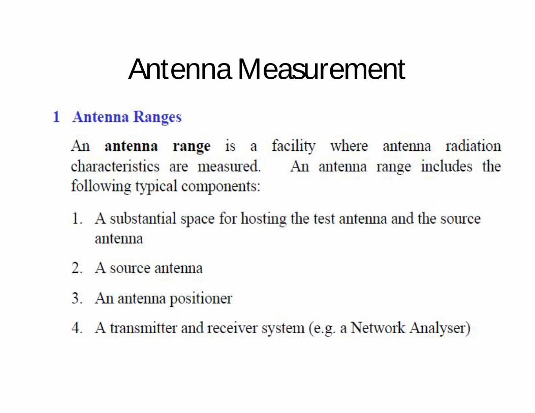
Antenna Measurement

Antenna Measurement

Gain Measurement

Radiation Pattern


