
UNIT -1 LINEAR WAVE SHAPPING - gvpcew.ac.ingvpcew.ac.in/Material/ECE/3 ECE - PDC UNIT - I.pdf ·...
64
GVPCEW UNIT -1 LINEAR WAVE SHAPPING Contents: High pass, Low pass circuits High pass and Low pass circuits response for: 1. Sine wave 2. Step 3. Pulse 4. Square 5. Ramp 6. Exponential High pass RC as differentiator Low pass RC as integrator Attenuators and its applications RL circuits RLC circuits Solved problems 1
Transcript of UNIT -1 LINEAR WAVE SHAPPING - gvpcew.ac.ingvpcew.ac.in/Material/ECE/3 ECE - PDC UNIT - I.pdf ·...

GVPCEW
UNIT -1
LINEAR WAVE SHAPPING
Contents:
High pass, Low pass circuits
High pass and Low pass circuits response for:
1. Sine wave
2. Step
3. Pulse
4. Square
5. Ramp
6. Exponential
High pass RC as differentiator
Low pass RC as integrator
Attenuators and its applications
RL circuits
RLC circuits
Solved problems
1
INTRODUCTION
Linear systems are those that satisfy both homogeneity and additivity.
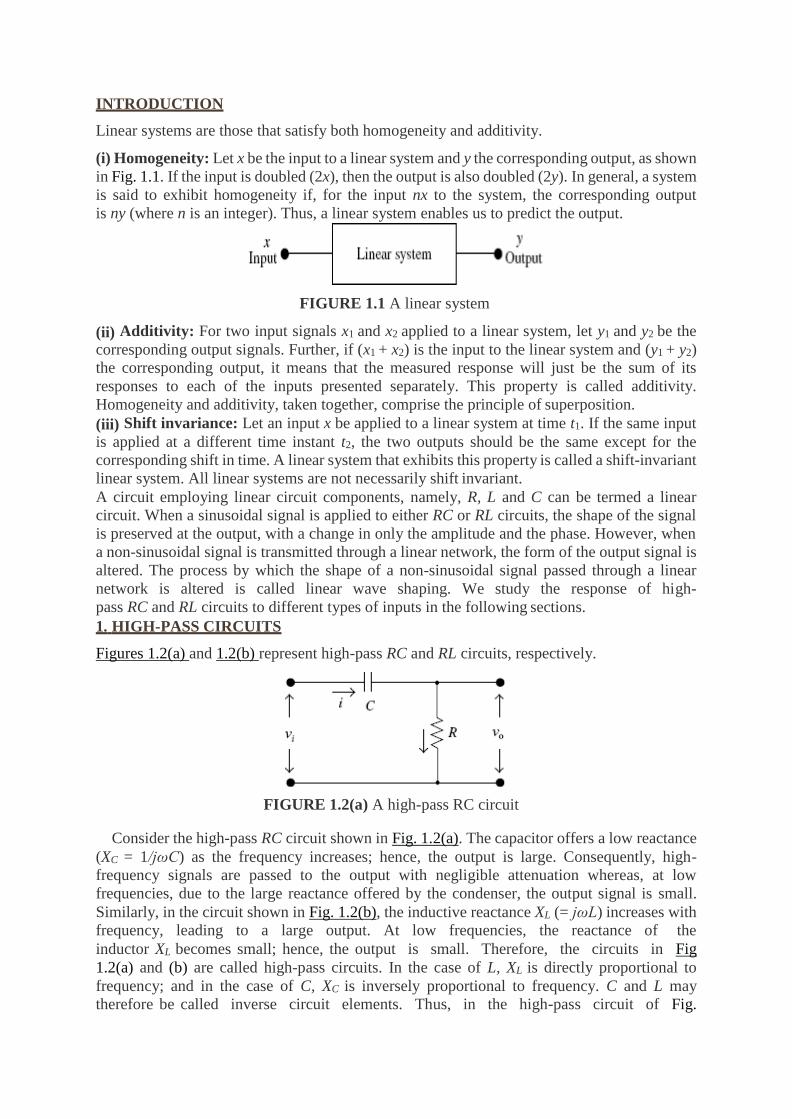
(i) Homogeneity: Let x be the input to a linear system and y the corresponding output, as shown
in Fig. 1.1. If the input is doubled (2x), then the output is also doubled (2y). In general, a system
is said to exhibit homogeneity if, for the input nx to the system, the corresponding output
is ny (where n is an integer). Thus, a linear system enables us to predict the output.
FIGURE 1.1 A linear system
(ii) Additivity: For two input signals x1 and x2 applied to a linear system, let y1 and y2 be the
corresponding output signals. Further, if (x1 + x2) is the input to the linear system and (y1 + y2)
the corresponding output, it means that the measured response will just be the sum of its
responses to each of the inputs presented separately. This property is called additivity.
Homogeneity and additivity, taken together, comprise the principle of superposition.
(iii) Shift invariance: Let an input x be applied to a linear system at time t1. If the same input
is applied at a different time instant t2, the two outputs should be the same except for the
corresponding shift in time. A linear system that exhibits this property is called a shift-invariant
linear system. All linear systems are not necessarily shift invariant.
A circuit employing linear circuit components, namely, R, L and C can be termed a linear
circuit. When a sinusoidal signal is applied to either RC or RL circuits, the shape of the signal
is preserved at the output, with a change in only the amplitude and the phase. However, when
a non-sinusoidal signal is transmitted through a linear network, the form of the output signal is
altered. The process by which the shape of a non-sinusoidal signal passed through a linear
network is altered is called linear wave shaping. We study the response of high-
pass RC and RL circuits to different types of inputs in the following sections.
1. HIGH-PASS CIRCUITS
Figures 1.2(a) and 1.2(b) represent high-pass RC and RL circuits, respectively.
FIGURE 1.2(a) A high-pass RC circuit
Consider the high-pass RC circuit shown in Fig. 1.2(a). The capacitor offers a low reactance
(XC = 1/jωC) as the frequency increases; hence, the output is large. Consequently, high-
frequency signals are passed to the output with negligible attenuation whereas, at low
frequencies, due to the large reactance offered by the condenser, the output signal is small.
Similarly, in the circuit shown in Fig. 1.2(b), the inductive reactance XL (= jωL) increases with
frequency, leading to a large output. At low frequencies, the reactance of the
inductor XL becomes small; hence, the output is small. Therefore, the circuits in Fig
1.2(a) and (b) are called high-pass circuits. In the case of L, XL is directly proportional to
frequency; and in the case of C, XC is inversely proportional to frequency. C and L may
therefore be called inverse circuit elements. Thus, in the high-pass circuit of Fig.

1.2(a), C appears as a series element; and in the high-pass circuit of Fig. 1.2(b), L appears as a
shunt element. The time constant τ is given by: τ = RC = L/R.
FIGURE 1.2(b) A high-pass RL circuit
What will be the response if different types of inputs such as sinusoidal, step, pulse, square
wave, exponential and ramp are applied to a high-pass circuit?
Response of the High-pass RC Circuit to Sinusoidal Input
Let us consider the response of a high-pass RC circuit, shown in Fig. 1.2(a) when a sinusoidal
signal is applied as the input. Here:
Let
where, τ = RC, the time constant of the circuit.
The signal undergoes a phase change and the phase angle, θ, is given by:
θ = tan−1 (ω1/ω) = tan−1 (T/τ)
At ω = ω1:
Hence, f1 is the lower half-power frequency of the high-pass circuit. The expression for the
output for the circuits in Figs. 1.2(a) and (b) is the same as given by Eq. (3). Figure 1.3(a) shows
a typical frequency–response curve for a sinusoidal input to a high-pass circuit. The frequency
response and the phase shift of the circuit shown in Fig. 1.2(a) are plotted in Figs.
1.3(b) and 1.3(c), respectively, for different values of τ.
From Fig. 1.3(b), it is seen that as the half-power frequency decreases for larger values of τ,
the gain curve shows a sharper rise. From Fig. 1.3(c), it is seen that if T/τ > 20, the phase angle
approaches approximately 90°.
Response of the High-pass RC Circuit to Step Input
A step voltage, shown in Fig.1.4(a), is represented mathematically as:

FIGURE 1.3(a) A typical frequency response curve for a sinusoidal input
A step is a sudden change in voltage, say at an instant t = 0, from say zero to V, in which
case, it is called a positive step. The voltage change could also be from zero to -V, in which
case it is called a negative step. This is an important signal in pulse and digital circuits. For
instance, consider an n–p–n transistor in the CE mode. Assume that VBE = 0. Then, the
voltageat the collector is approximately VCC. Now if a battery with voltage Vσ is
connected so that VBE = Vσ, as the device is switched ON, the voltage at the collector which
earlier was VCC, now falls to VCE(sat). This means a negative step is generated at the collector.
However, if the transistor is initially turned ON so that the voltage at its collector is VCE(sat)
and VBE is made zero, then as the transistor is switched OFF, the voltage at its collector rises
to VCC. A positive step is now generated at its collector.
For a step input, let the output voltage be of the form:
where, τ = RC, the time constant of the circuit.
FIGURE 1.3(b) The frequency–response curve for different values of τ

FIGURE 1.3(c) Phase versus frequency curve for different values of τ
B1 is the steady-state value of the output voltage because as t → ∞, vo → B1.
Let the final value of this output voltage be called vf. Then:
B2 is determined by the initial output voltage. At t = 0, when the step voltage is applied, the
change at the output is the same as the change at the input, because a capacitor is connected
between the input and the output. Hence,
Therefore,
B2 = vi − B1
Using Eq. (6):
Substituting the values of B1 and B2 from Eqs. (6) and (8) respectively in Eq. (5), the general
solution is given by the relation:
For a high-pass RC circuit, let us calculate vi and vf. As the capacitor blocks the dc component
of the input, vf = 0. Since the capacitor does not allow sudden voltage changes, a change in the
voltage of the input signal is necessarily accompanied by a corresponding change in the voltage
of the output signal. Hence, at t = 0+ when the input abruptly rises to V, the output also changes
by V.
Therefore, vi = V.
Substituting the values of vf and vi in Eq. (9):

initial value is called the fall time. It indicates how fast the output reaches its steady-state value.
v0(t)/V for x varying from 0 to 5 is shown in Table 1.1. The response of the circuit is plotted in
Fig. 1.4(b).
At t = 0, when a step voltage V is applied as input to the high-pass circuit, as the capacitor
will not allow any sudden changes in voltage, it behaves as a short circuit. Hence, the input
voltage V appears at the output. As the input remains constant, the charge on the capacitor
discharges exponentially with the time constant τ. After approximately 5τ, when τ is small, the
output reaches the steady-state value. As τ becomes large, it takes a longer time for the charge
on the capacitor to decay; hence, the output takes longer to reach the steady-state value. In
general, the response of the circuit to different types of inputs is obtained by formulating the
differential equation and solving for the output.
For the circuit in Fig. 1.2(a):
But vo = iR
For a step input, put vi = V and RC = τ. Taking Laplace transforms:
Taking Laplace inverse:
Fall time (tf): When a step voltage V is applied to a high-pass circuit, the output suddenly
changes as the input and then the capacitor charges to V. Once the capacitor C is fully charged,
it behaves as an open circuit for the dc input signal. Hence, in the steady-state, the output should
be zero. However, the output does not reach this steady-state instantaneously; there is some
time delay before the voltage on the capacitor decays and reaches the steady-state value. The
time taken for the output voltage to fall from 90 per cent of its initial value to 10 per cent of its
The output voltage at any instant, in the high-pass circuit is given by Eq. (17). At t = t1, vo(t1)
= 90% of V = 0.9 V. Therefore,

0.9 = e−t1
/τ et1/τ = 1/0.9 = 1.11 t1/τ = ln(1.11)
t1 = τln (1.11) = 0.1τ
At t = t2, vo(t) = 10% of V = 0.1 V. Hence,
0.1 = e−t2/τ et2/τ = 1/0.1 = 10 t2 = τ ln (10) = 2.3τ
The fall time is calculated as:
The lower half-power frequency of the high-pass circuit is:
Hence, the fall time is inversely proportional to f1, the lower half-power frequency. As f1, is
inversely proportional to τ, the shape of the signal at the output changes with τ.
Response of the High-pass RC Circuit to Pulse Input
A positive pulse is mathematically represented as the combination of a positive step followed
by a delayed negative step i.e., vi = Vu(t) − Vu(t − tp) where, tp is the duration of the pulse as
shown in Fig. 1.6.
To understand the response of a high-pass circuit to this pulse input, let us trace the sequence
of events following the application of the input signal.
At t = 0, vi abruptly rises to V. As a capacitor is connected between the input and output, the
output also changes abruptly by the same amount. As the input remains constant, the output
decays exponentially to V1 at t = tp. Therefore,
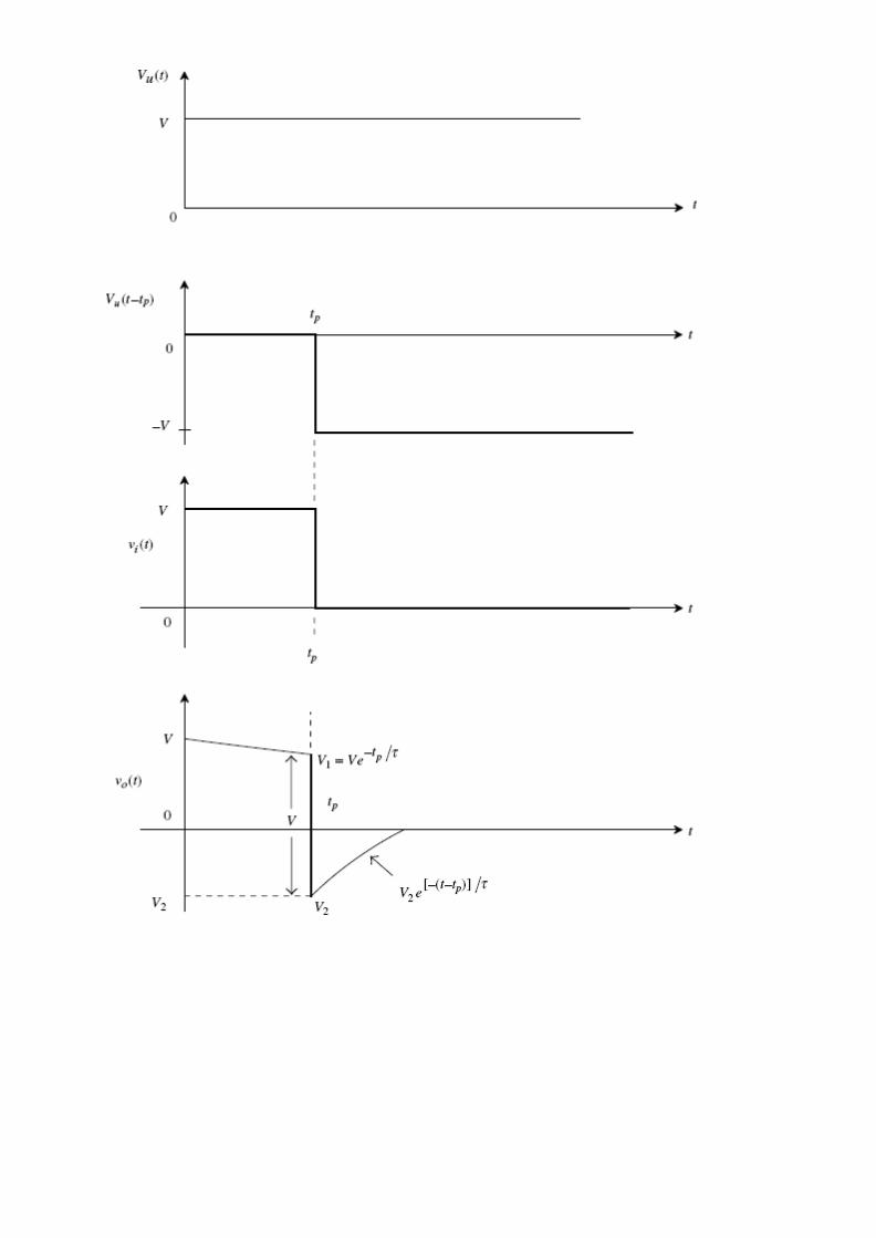

FIGURE 1.6 Pulse input and output of a high-pass circuit
At t = tp, the input abruptly falls by V, vo also falls by the same amount. In other
words, vo = V1 − V. Since V1 is less than V; vo is negative and its value is V2 and this decays to
zero exponentially. For t > tp,
Substituting Eq. (22) in Eq. (23):
The response of high-pass circuits with different values of τ to pulse input is plotted in Fig.
1.7. As is evident from the preceding discussion, when a pulse is passed through a high-pass
circuit, it gets distorted. Only when the time constant τ is very large, the shape of the pulse at
the output is preserved, as can be seen from Fig. 1.7(b). However, as shown in Fig. 1.7(c),
when the time constant τ is neither too small nor too large, there is a tilt (also called a sag) at
the top of the pulse and an under-shoot at the end of the pulse. If τ << tp, as in Fig. 1.7(d), the
output comprises a positive spike at the beginning of the pulse and a negative spike at the end
of the pulse. In other words, a high-pass circuit converts a pulse into spikes by employing a
small time constant; this process is called peaking.
If the distortion is to be negligible, τ has to be significantly larger than the duration of the
pulse. In general, there is an undershoot at the end of the pulse. The larger the tilt (for small τ),
the larger the undershoot and the smaller the time taken for this undershoot to decay to zero.
The area above the reference level (A1) is the same as the area below the reference level (A2).
Let us verify this using Fig. 1.8.
Area A1: For 0 < t < tp:
vo = Ve−t/τ
Similarly,

From Eqs. (25) and (26) it is evident that

FIGURE 1.7 The response of a high-pass circuit to a pulse input
FIGURE 1.8 The calculation of A1 and A2
EXAMPLE
Example 1: A pulse of amplitude 10 V and duration 10 μs is applied to a high-pass RC circuit.
Sketch the output waveform indicating the voltage levels for (i) RC = tp, (ii) RC = 0.5tp and
(iii) RC = 2tp.
Solution:
1. When RC = tp = τ
At t = tp
V1 = 10 e−(10×10−6)/(10×10−6) = 10−1 = 3.678 V
vo1 = 10 e−t/(10×10−6) for t < tp
vo(t > tp) = (V1 − 10)e−(t−10 × 10−6)/(10 × 10−6) = −6.322 e−(t−10 × 10−6)/(10 × 10−6)
2. When RC = τ = 0.5tp
At t = tp
V1 = 10 e−(10 × 10−6)/(0.5 × 10 × 10−6) = 10e−2 = 1.35 V
vo1 = 10 e−t/(0.5 × 10 × 10−6) for t < tp
vo(t > tp) = −8.65 e−(t−10 × 10−6)/(0.5 × 10 × 10−6)
3. When RC = τ = 2tp
At t = tp
V1 = 10 e(−10 × 10−6)/(2 × 10 × 10−6) = 10e−0.5 = 6.05 V
vo1 = 10 e−t/(2 × 10 × 10−6) for t < tp
vo(t > tp) = −3.935 e−(t−10 × 10−6)/(2 × 10 × 10−6)
14

even if the signal at the input is referenced to an arbitrary dc level, the output is always
Based on these results, the output waveforms are sketched as in Fig.
1.9(a), (b) and (c) corresponding to cases (i), (ii) and (iii), respectively.
FIGURE 1.9(b) The response of a high-pass circuit for different values of τ
From Example 2.2, it is seen that when τ is large, the amplitude distortion in the output is
minimal, i.e., the shape of the signal is almost preserved in the output. As the value
of τ decreases, the charge on the capacitor decreases by a larger amount during the period the
input remains constant. Consequently, the output is distorted. If τ decreases still further, it can
be seen that the output contains positive and negative spikes. The shape of the signal in the
output is essentially decided by the time constant of the circuit.
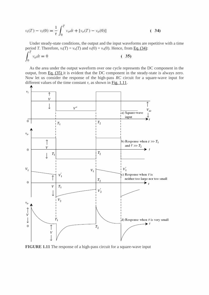
Response of the High-pass RC Circuit to Square-wave Input
A waveform that has a constant amplitude, say, V′ for a time T1 and has another constant
amplitude, V ″ for a time T2, and which is repetitive with a time T = (T1 + T2), is called a square
wave. In a symmetric square wave, T1 = T2 = T/2. Figure 1.10 shows typical input–output
waveforms of the high-pass circuit when a square wave is applied as the input signal.
As the capacitor blocks the DC, the DC component in the output is zero. Thus, as expected,
15

referenced to the zero level. It can be proved that whatever the dc component associated with
a periodic input waveform, the dc level of the steady-state output signal for the high-pass circuit
is always zero as shown in Fig. 1.10. To verify this statement, we write the KVL equation for
the high-pass circuit:
where, q is the charge on the capacitor. Differentiating with respect to t:
But
Substituting this condition in Eq. (29):
Since vo = iR, i = vo/R and RC = τ. Therefore,
Multiplying by dt and integrating over the time period T we get:
FIGURE 1.10 A typical steady-state output of a high-pass circuit with a square wave as input
From Eqs. (30), (31), (32) and (33):
Under steady-state conditions, the output and the input waveforms are repetitive with a time
period T. Therefore, vi(T) = vo(T) and vi(0) = vo(0). Hence, from Eq. (34):
As the area under the output waveform over one cycle represents the DC component in the
output, from Eq. (35) it is evident that the DC component in the steady-state is always zero.
Now let us consider the response of the high-pass RC circuit for a square-wave input for
different values of the time constant τ, as shown in Fig. 1.11.
FIGURE 1.11 The response of a high-pass circuit for a square-wave input

As is evident from the waveform in Fig. 1.11(b), there is no appreciable distortion in the
output if τ is large. The output is almost the same as the input except for the fact that there is
no DC component in the output. As τ decreases, as in Fig. 1.11(c), there is a tilt in the positive
duration (amplitude decreases from V1 to V1′ during the period 0 to T1) and there is also a tilt in
the negative duration (amplitude increases from V2 to V2′ during the period T1 to T2). A further
decrease in the value of τ [see Fig. 1.11(d)] gives rise to positive and negative spikes. There is
absolutely no resemblance between the signals at the input and the output. However, this
condition is imposed on high-pass circuits to derive spikes. In case a pulse is required to trigger
another circuit, we see that the pulses obtained either at the rising edge (positive spike) or at
the trailing edge (negative spike) may be used to edge trigger a flip-flop, as discussed in later
chapters in the book. Let us consider the typical response of the high-pass circuit for a square-
wave input shown in Fig. 1.12.
FIGURE 1.12 The typical response of a high-pass RC circuit for a square-wave input
From Fig. 1.12 and using Eq. (17) we have:
For a symmetric square wave T1 = T2 = T/2. And, because of symmetry:
From Eq. (36):
But
Therefore,
V1e−T /τ −T /τ
From Eq. (37):
V1 = −V2
Substituting in Eq. (38):
1 + V1 = V V1(1 + e 1 ) = V
Thus,
For a symmetric square wave, as T1 = T2 = T/2, Eq. (2.39) is written as:
But
There is a tilt in the output waveform. The percentage tilt, P, is defined as:
If T/2τ << 1,
Therefore,
Thus, for a symmetrical square wave:

Equation (45) tells us that the smaller the value of τ when compared to the half-period of the
square wave (T/2), the larger is the value of P. In other words, distortion is large with
small τ and is small with large τ. The lower half-power frequency, f1 = 1/2πτ.
Therefore,
Putting in Eq. (45)
P = πf1T × 100%
Therefore,
Let us calculate and plot the response by taking specific examples.
EXAMPLE
Example 3: A 10 Hz square wave whose peak-to-peak amplitude is 2 V is fed to an amplifier.
Calculate and plot the output waveform if the lower 3-dB frequency is 0.3 Hz.
Solution: Let C be the condenser through which the signal is connected to the amplifier, having
an input resistance R, as shown in Fig. 1.13(a). This is essentially the high-pass circuit in Fig.
1.1(a).
The lower 3-dB frequency f1 = 0.3 Hz
Input frequency is f = 10 Hz
FIGURE 1.13(a) The coupling network and (b) The response of the circuit
Therefore,
The response of the circuit is shown in Fig. 1.13(b).
EXAMPLE
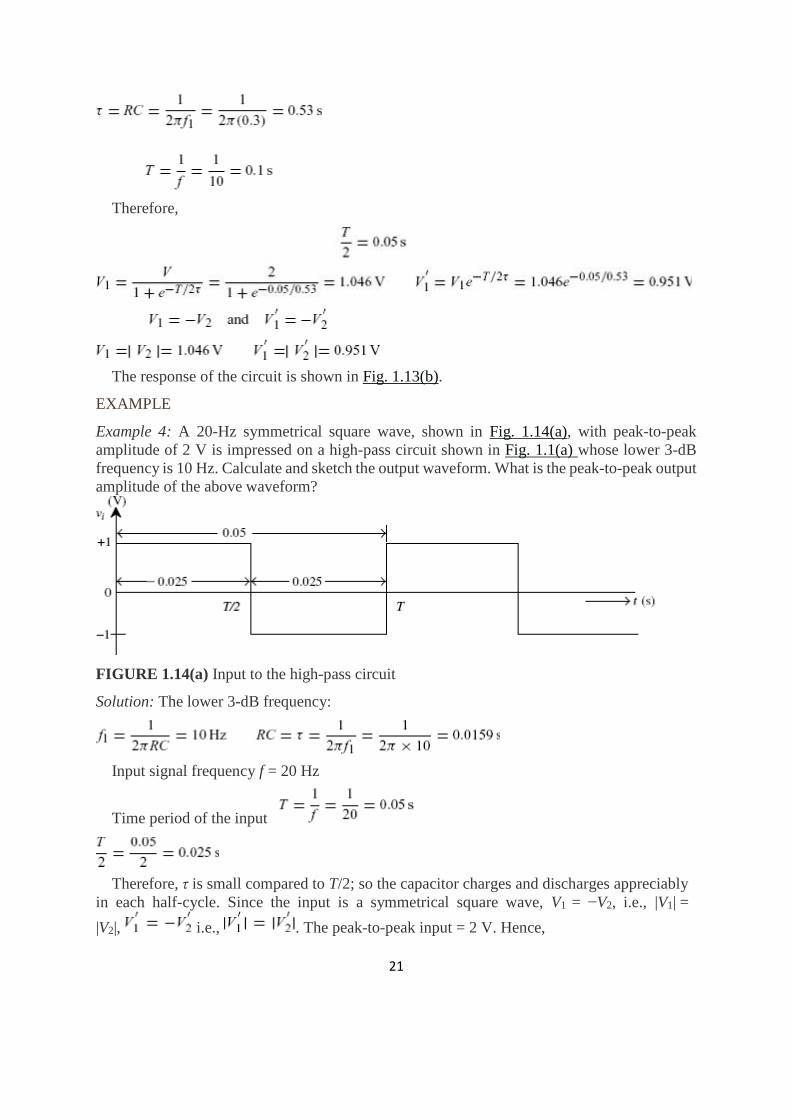
Example 4: A 20-Hz symmetrical square wave, shown in Fig. 1.14(a), with peak-to-peak
amplitude of 2 V is impressed on a high-pass circuit shown in Fig. 1.1(a) whose lower 3-dB
frequency is 10 Hz. Calculate and sketch the output waveform. What is the peak-to-peak output
amplitude of the above waveform?
FIGURE 1.14(a) Input to the high-pass circuit
Solution: The lower 3-dB frequency:
Input signal frequency f = 20 Hz
Time period of the input
Therefore, τ is small compared to T/2; so the capacitor charges and discharges appreciably
in each half-cycle. Since the input is a symmetrical square wave, V1 = −V2, i.e., |V1| =
|V2|, i.e., . The peak-to-peak input = 2 V. Hence,
21

Peak-to-peak value of output = V1 − V2 = 3.312 V.
= V1e(−T/2)/τ = 1.656 e−(0.025/0.0159) = 0.344 V
The output is plotted in Fig. 1.14(b).
FIGURE 1.14(b) Output of the high-pass circuit for the given
input
FIGURE 1.15 The output of the high-pass circuit for the specified input
Response of the High-pass RC Circuit to Exponential Input
When a pulse is applied as input to an amplifier, it may while appearing at the actual input
terminals of the amplifier, have a finite rise time. The result is that the input to the amplifier is

no longer a pulse with sharp rising edge, but an exponential. We would now like to know the
response of the high-pass circuit to this exponential input. If the input to the high-pass circuit
in Fig.1.2(a) is an exponential of the form:
where, τ1 is the time constant of the circuit that has generated the exponential signal as shown
in Fig. 1.16(a).
From Eq. (30), we know:
As vi = V(1 − e−t/τ1),
Substituting Eq. (2.48) in Eq. (2.30):
FIGURE 1.16(a) Exponential input
Taking Laplace transforms:
where, τ is the time constant of the high-pass circuit.
Therefore,
Case 1: τ = τ1
Applying partial fractions, Eq. (50) can be written as:
Therefore,
Put s = −1/τ1 in Eq. (52).
Now put s = −1/τ in Eq. (52). Then:
Therefore,
Substituting the values of A and B in Eq. (51):
Taking inverse Laplace transform:
This is the expression for the output voltage where τ ≠ τ1.
Let t/τ1 = x and τ/τ1 = n. For n ≠ 1, i.e., τ ≠ τ1, we have from Eq. (54):
Therefore,
If τ >> τ1, the second term in the Eq. (2.55) is small when compared to the first. Thus,
Case 2: τ = τ1, that is, n = 1.
Taking Laplace inverse:
As t/τ = x = t/τ1 and τ/τ1 = n = 1:
The response of the circuit is plotted for different values of n in Fig. 1.16(b).
From the response in Fig.1.16(b), it is seen that near the origin the output follows the input.
Also, the smaller the value of n (= τ/τ1 is small), the smaller is the output peak and the shorter
is the duration of the pulse. As n increases, the peak becomes larger and the duration of the
pulse becomes longer. Hence, the choice of n is based on the amplitude and duration of the
pulse required for a specific application. The maximum output occurs when (dvo/dt) = 0.
From Eq. (55):
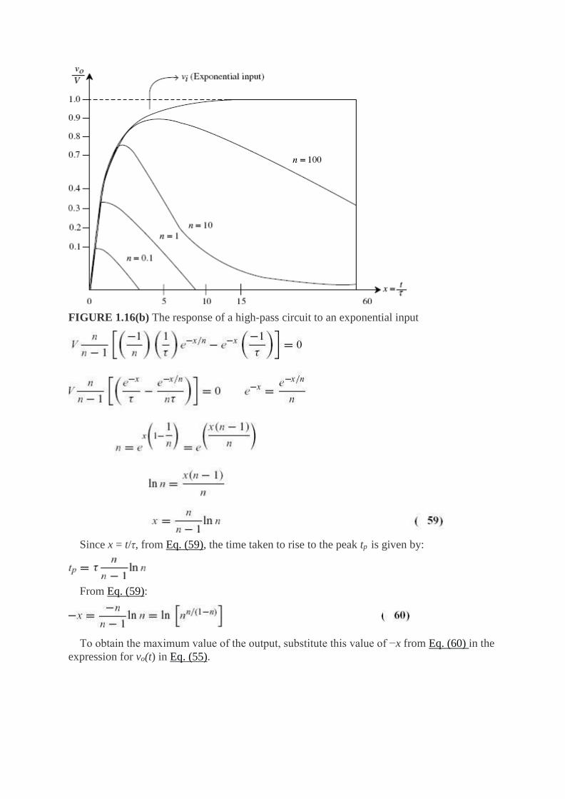
FIGURE 1.16(b) The response of a high-pass circuit to an exponential input
Since x = t/τ, from Eq. (59), the time taken to rise to the peak tp is given by:
From Eq. (59):
To obtain the maximum value of the output, substitute this value of −x from Eq. (60) in the
expression for vo(t) in Eq. (55).
From the waveforms in Fig. 1.16(b) and the subsequent mathematical relations derived, it is seen that, if
an exponential signal is applied as an input to a high-pass circuit, the output is a pulse whose duration
depends on n(= τ/τ1), where τ1 is the time constant of the previous circuit that has generated the exponential
signal and τ is the time constant of the high-pass circuit under consideration. The smaller the value of n, the
smaller the duration of this output pulse and also the smaller its amplitude. As n increases, the duration as
well as the amplitude of this output pulse increases. Hence, depending on our requirement, we adjust the
value of n.
it for the given exponential input when τ = τ1

The input and the output waveforms are as shown in Fig. 1.17.
FIGURE 1.17 The input to and the output of the high-pass circuit
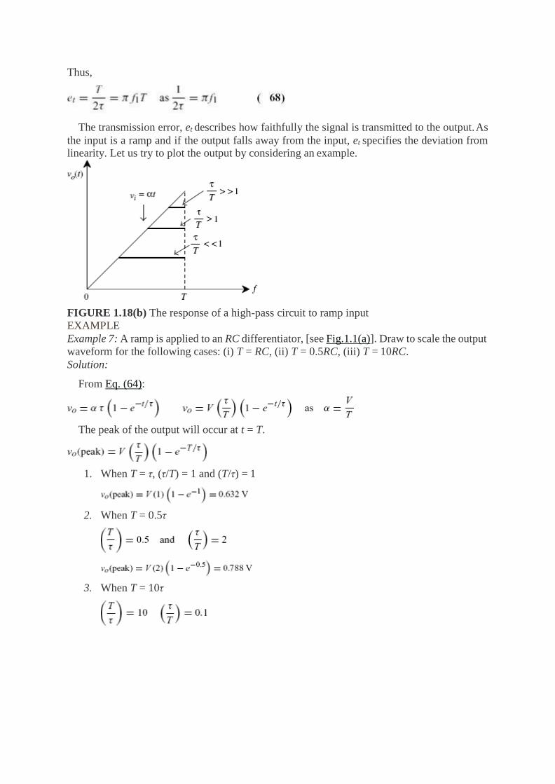
Response of the High-pass RC Circuit to Ramp Input
Ramp is a waveform in which the voltage increases linearly with time, for t > 0, and is zero
for t < 0. It is used to move the spot in a CRO linearly with time along the x-axis. This type of
waveform is generated by sweep circuits which we shall study later. However, if a ramp is
applied as an input to a high-pass circuit, there could be deviation from linearity in the ouput.
We can calculate and plot the ouput for different values of τ to understand how it influences
the output. Let the input to the high-pass circuit be vi = αt where, α is the slope, as shown in Fig.
1.18(a).
For the high-pass circuit, we have:
FIGURE 1.18(a) Ramp input
Taking Laplace transforms:
Multiplying throughout by s:
Therefore,
From which, A = ατ and B = −ατ
Taking Laplace inverse:
If t/τ << 1:
Therefore, vo(t) = ατ
The output falls away from the input, as shown in Fig. 1.18(b). From the waveforms in Fig.
1.18(b), we see that for the output to be the same as the input, τ >> T (the duration of the ramp).
As the value of τ decreases, not only the amplitude of the output decreases but also the signal
now is an exponential. The output falls away from the input. So, the choice of τ is dictated by
the specific application. Transition error defines deviation from linearity and is given by:
At t = T, vi = αT and vo = αT[1 − (T/2τ)]. Therefore,
Thus,
The transmission error, et describes how faithfully the signal is transmitted to the output. As
the input is a ramp and if the output falls away from the input, et specifies the deviation from
linearity. Let us try to plot the output by considering an example.
FIGURE 1.18(b) The response of a high-pass circuit to ramp input
EXAMPLE
Example 7: A ramp is applied to an RC differentiator, [see Fig.1.1(a)]. Draw to scale the output
waveform for the following cases: (i) T = RC, (ii) T = 0.5RC, (iii) T = 10RC.
Solution:
From Eq. (64):
The peak of the output will occur at t = T.
1. When T = τ, (τ/T) = 1 and (T/τ) = 1
2. When T = 0.5τ
3. When T = 10τ
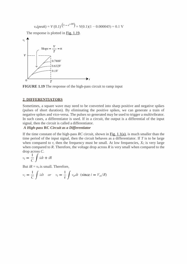
vo(peak) = V (0.1) = V(0.1)(1 − 0.000045) = 0.1 V
The response is plotted in Fig. 1.19.
FIGURE 1.19 The response of the high-pass circuit to ramp input
2. DIFFERENTIATORS
Sometimes, a square wave may need to be converted into sharp positive and negative spikes
(pulses of short duration). By eliminating the positive spikes, we can generate a train of
negative spikes and vice-versa. The pulses so generated may be used to trigger a multivibrator.
In such cases, a differentiator is used. If in a circuit, the output is a differential of the input
signal, then the circuit is called a differentiator.
A High-pass RC Circuit as a Differentiator
If the time constant of the high-pass RC circuit, shown in Fig. 1.1(a), is much smaller than the
time period of the input signal, then the circuit behaves as a differentiator. If T is to be large
when compared to τ, then the frequency must be small. At low frequencies, XC is very large
when compared to R. Therefore, the voltage drop across R is very small when compared to the
drop across C.
But iR = vo is small. Therefore,
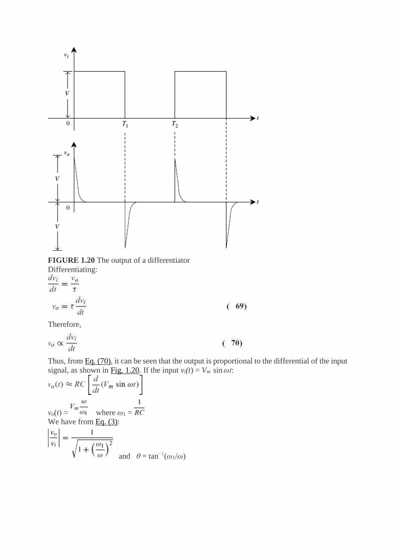
FIGURE 1.20 The output of a differentiator
Differentiating:
Therefore,
Thus, from Eq. (70), it can be seen that the output is proportional to the differential of the input
signal, as shown in Fig. 1.20. If the input vi(t) = Vm sin ωt:
vo(t) ≈ where ω1 =
We have from Eq. (3):
and θ = tan−1(ω1/ω)
When θ = 90°, the sine function at the input becomes a cosine function at the output, as is
required in a differentiator. When ω1/ω = 100, θ = 89.4° which is nearly equal to 90°. Hence,
a high-pass circuit behaves as a good differentiator only when RC << T, and the output is a co-
sinusiodally varying signal if the input is a sine wave. If the input is a square wave, the output
is in the form of positive and negative spikes, as shown in Fig.1.20.
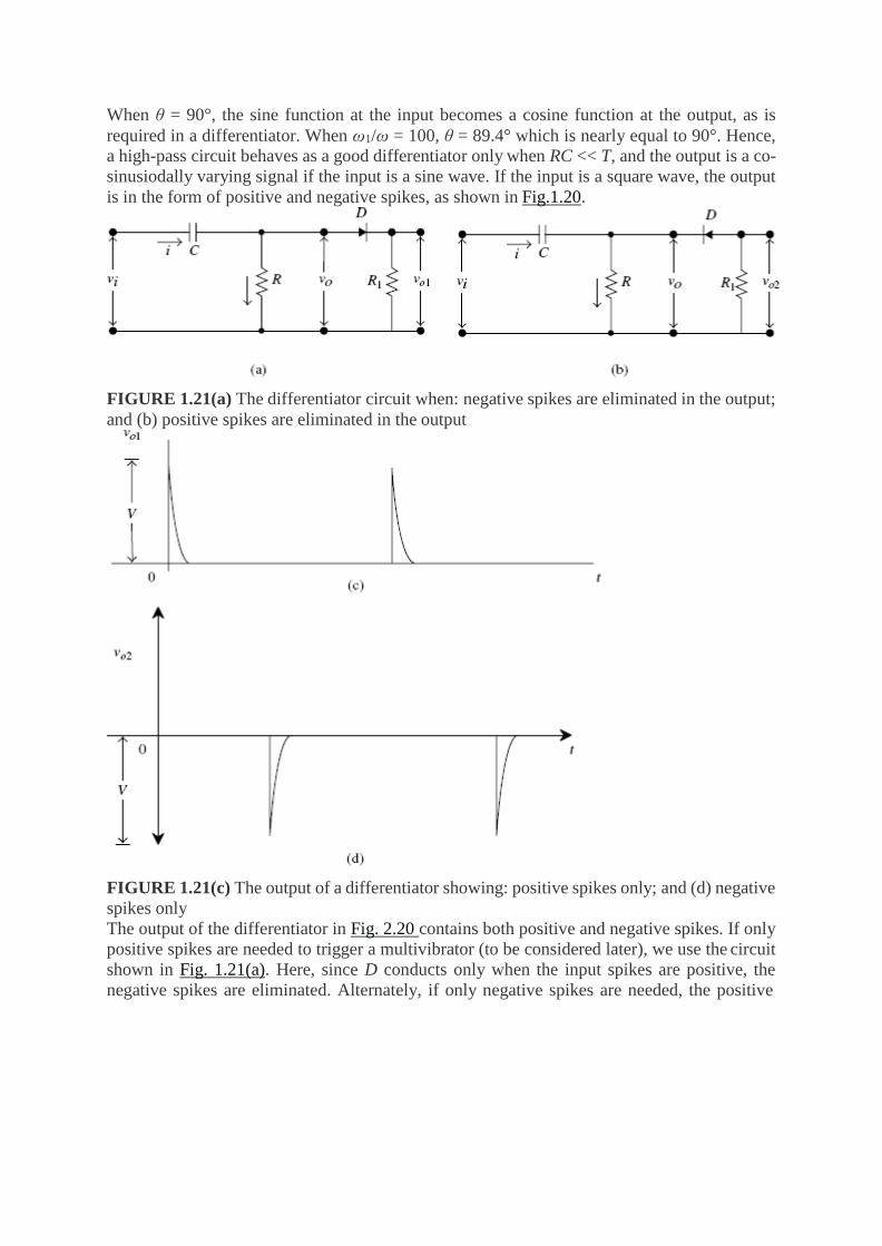
FIGURE 1.21(a) The differentiator circuit when: negative spikes are eliminated in the output;
and (b) positive spikes are eliminated in the output
FIGURE 1.21(c) The output of a differentiator showing: positive spikes only; and (d) negative
spikes only
The output of the differentiator in Fig. 2.20 contains both positive and negative spikes. If only
positive spikes are needed to trigger a multivibrator (to be considered later), we use the circuit
shown in Fig. 1.21(a). Here, since D conducts only when the input spikes are positive, the
negative spikes are eliminated. Alternately, if only negative spikes are needed, the positive

spikes are eliminated using the circuit in Fig. 1.21(b), since D conducts only when the input
spikes are negative. The output of the circuit in Fig. 1.21(a) is shown in Fig. 1.21(c). Similarly,
the output of the circuit in Fig. 1.21(b) is shown in Fig. 1.21(d).
An Op-amp as a Differentiator
An operational amplifier, commonly known as an op-amp, can be used as a differentiator, as
shown inFig. 1.22(a).
FIGURE 1.22(a) Op-amp as a differentiator
FIGURE 1.22(b) The op-amp differentiator circuit resulting from the use of Miller’s theorem
From Miller’s theorem:
where A is the gain of the amplifier. The resistance, R, appears between the input and output
terminals of the op-amp. Using Miller’s theorem, R can be replaced
by R1 and R2 as R1 = R/(1− A) is small since Ais large; and R2 = RA/(A − 1) = R since A is large.
Hence, the op-amp circuit can be redrawn as shown in Fig. 1.22(b).
For a good differentiator, τ (= R1C) should be small. As R1 is a very small value of resistor
(since A is large), an op-amp differentiator behaves as a better differentiator when compared to
a simple RC differentiator, without physically reducing the value of R.
Double Differentiators
The circuit in Fig. 1.23 is called a double differentiator as we have two high-pass differentiating
circuits. In the figure, A is the gain of the inverting amplifier. Here, R1C1 = τ1 and R2C2 = τ2 are
small when compared to the time period of the input signal.
Let the input to the circuit be a ramp, i.e., vi = αt. From Eq. (64), the output of the first high-
pass R1C1circuit for the ramp input is:
Therefore, the output voltage of the amplifier v is written as:
where, A is the amplifier gain. It can be seen from Eq. (72) that v has phase inversion. The
output of the first high-pass circuit, which is an exponential, is the input to the second
differentiator. We know from Eq. (55) that the output of this second differentiator is a pulse.

FIGURE 1.23 A double differentiator
where n = τ2/τ1 and x = t/τ1. So,
Therefore,
For n = 1
The ramp voltage which is input to the double differentiator is converted to a pulse. The
response is plotted in Fig. 1.24. From Eq. (1.75), the output for τ = τ1 = τ2 is given as:
From Eq. (72) the output of the amplifier v is given as:
v = −Aατ1 (1 − e−t/τ1)

FIGURE 1.24 The response of a double differentiator to a ramp input
The initial slope of this output is:
From Eq. (71), we have:
v1 = ατ (1 − e−t/τ)
The initial slope of the output of the first differentiator (input to the amplifier) is:
We see from Eqs. (77) and (78), the initial slope of the input to the amplifier v1 is α, whereas
the initial slope of the amplifier output v is Aα. The output rises much faster than the input, as
shown in Fig. 1.24. Hence, the amplifier is called a rate-of-rise amplifier. At this point, it is
relevant to talk about a comparator. A circuit that compares the input with a reference and tells
us the instant at which the input has reached the reference level is called a comparator. One
such simple and practical comparator is a diode comparator. Sometimes a circuit needs to be

activated the moment the input reaches a predetermined level. The diode comparator will not
be able to do this job. Thus, the output of the diode comparator is given as the input to the
double differentiator. As the output of the double differentiator is a pulse whose amplitude and
duration can be controlled, this output can activate the desired circuit. We discuss this aspect
in greater details in later chapters.
2.1 THE RESPONSE OF A HIGH-PASS RL CIRCUIT TO STEP INPUT
A high-pass RL circuit is represented in Fig. 2.2(b). If a step of magnitude V is applied, let us
find the response. Writing the KVL equation:
Therefore, from Eq. (80)
As vi = V, Eq. (2.79) can also be written as:
Applying Laplace transforms:
Taking Laplace inverse:
Similarly, the response of this circuit is evaluated for other inputs. This high-pass circuit is
used as a differentiator if L/R T. Since vo = Ldi/dt, and i ≈ vi/R:
SOLVED PROBLEMS
Example 8: The output of a step generator has an amplitude of 10 V and rise-time of 1.1 ns.
When this is applied as an input to a high-pass circuit with R = 100 Ω [see Fig 1.25(a)], there
appears across R a pulse of amplitude 1 V. Find the value of the capacitance.
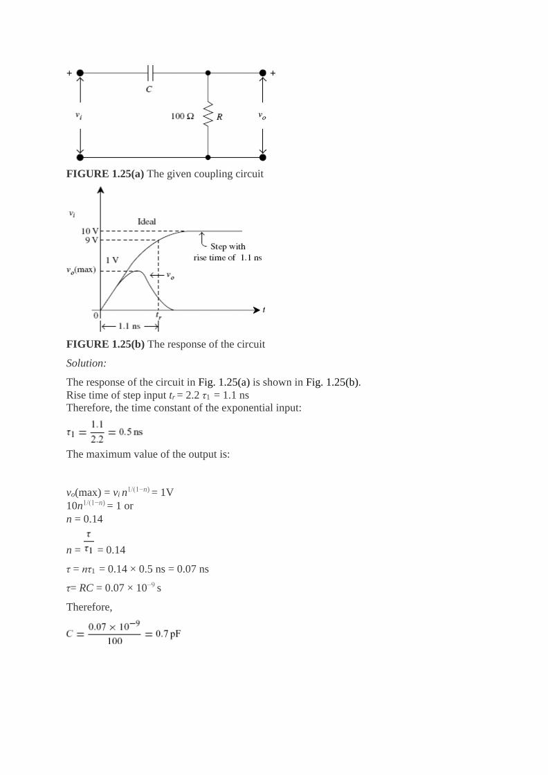
FIGURE 1.25(a) The given coupling circuit
FIGURE 1.25(b) The response of the circuit
Solution:
The response of the circuit in Fig. 1.25(a) is shown in Fig. 1.25(b).
Rise time of step input tr = 2.2 τ1 = 1.1 ns
Therefore, the time constant of the exponential input:
The maximum value of the output is:
vo(max) = vi n1/(1−n) = 1V
10n1/(1−n) = 1 or
n = 0.14
n = = 0.14
τ = nτ1 = 0.14 × 0.5 ns = 0.07 ns
τ= RC = 0.07 × 10⁻⁹ s
Therefore,

Example 9: A limited ramp from a generator rises linearly to Vs in a time period Ts = 0.1 μs and
remains constant for 2 μs. This signal is applied to a differentiating circuit whose time constant
is 0.01μs. The resultant pulse at the output of the differentiator has a maximum value of 15 V.
What is the peak amplitude of the ramp at the output of the generator?
Solution:
RC = τ = 0.01 μs = 0.01 × 10⁻⁶ s
vo(max) = 15 V
ατ = vo(max) = 15 V
Ts = 0.1 μs
The peak value of the ramp from the generator is:
Vs = αTs = × 0.1 × 10−6 = 150 V
The input and output are plotted in Fig. 2.26.
FIGURE 1.26 The input and the output for the specified conditions
3) LOWPASS CIRCUIT
3.1 INTRUDUCTION
A low-pass circuit is one which gives an appreciable output for low frequencies and zero or
negligible output for high frequencies. In this chapter, we essentially consider low-
pass RC and RL circuits and their responses to different types of inputs. Also, we study

attenuators that reduce the magnitude of the signal to the desired level. Attenuators which give
an output that is independent of frequency are studied. One application of such a circuit is as a
CRO probe. Further, the response of the RLC circuit to step input is considered and its output
under various conditions such as under-damped, critically damped and over-damped conditions
is presented. The application of an RLC circuit as a ringing circuit is also considered.
3.2 LOW-PASS CIRCUITS
Low-pass circuits derive their name from the fact that the output of these circuits is larger for
lower frequencies and vice-versa. Figures 3.1(a) and (b) represent a low-pass RC circuit and a
low-pass RL circuit, respectively.
In the RC circuit, shown in Fig. 3.1(a), at low frequencies, the reactance of C is large and
decreases with increasing frequency. Hence, the output is smaller for higher frequencies and
vice-versa. Similarly, in the RL circuit shown in Fig. 3.1(b), the inductive reactance is small
for low frequencies and hence, the output is large at low frequencies. As the frequency
increases, the inductive reactance increases; hence, the output decreases. Therefore, these
circuits are called low-pass circuits. Let us consider the response of these low-pass circuits to
different types of inputs.
FIGURE 3.1(a) A low-pass RC circuit; and (b) a low-pass RL circuit
3.2.1 The Response of a Low-pass RC Circuit to Sinusoidal Input
For the circuit given in Fig. 3.1(a), if a sinusoidal signal is applied as the input, the output vo is
given by the relation:
where, ω2 = 1/CR = 1/τ. From Eq. (3.1), the phase shift θ the signal undergoes is given as:
θ = tan−1(ω/ω2) = tan−1(τ/T)
Figure 3.2(a) shows a typical frequency vs. gain characteristic. Hence, f2 is the upper half-
power frequency. At ω = ω2,
Figure 3.2(b) shows the variation of gain with frequency for different values of τ. As is
evident from the figure, the half-power frequency, f2, increases with the decreasing values of τ,
the time constant. The sinusoidal signal undergoes a change only in the amplitude but its shape
remains preserved.
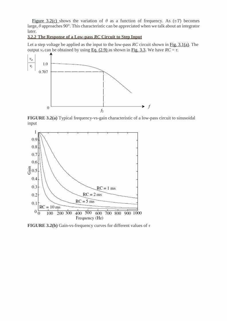
Figure 3.2(c) shows the variation of θ as a function of frequency. As (τ/T) becomes
large, θ approaches 90°. This characteristic can be appreciated when we talk about an integrator
later.
3.2.2 The Response of a Low-pass RC Circuit to Step Input
Let a step voltage be applied as the input to the low-pass RC circuit shown in Fig. 3.1(a). The
output vo can be obtained by using Eq. (2.9) as shown in Fig. 3.3. We have RC = τ.
FIGURE 3.2(a) Typical frequency-vs-gain characteristic of a low-pass circuit to sinusoidal
input
FIGURE 3.2(b) Gain-vs-frequency curves for different values of τ

FIGURE 3.2(c) Phase-vs-frequency curves for different values of τ
vo(t) = vf + (vi − vf) e−t/τ
Here, vf = V and vi = 0. Therefore,
As t → ∞, vo(t) → V.
Initially, as the capacitor behaves as a short circuit, the output voltage is zero. As the
capacitor charges, the output reaches the steady-state value of V in a time interval that is
dependent on the time constant, τ. On the other hand, the output of Eq. (3.2) can also be
obtained by solving the following differential equation. From Fig. 3.1(a), For vi = V:
FIGURE 3.3 The response of a low-pass circuit to step input
We know that (1/C) ∫ idt = vo
From Eqs. (3.3) and (3.4):
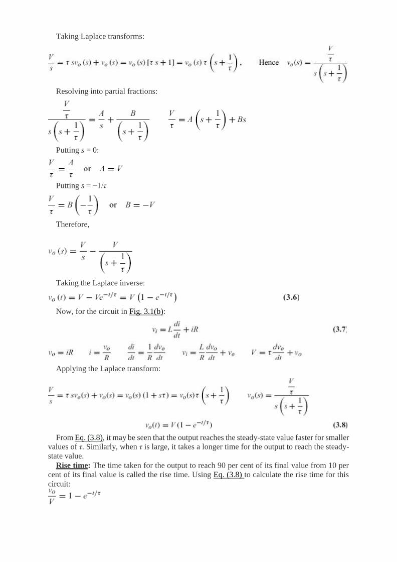
Taking Laplace transforms:
Resolving into partial fractions:
Putting s = 0:
Putting s = −1/τ
Therefore,
Taking the Laplace inverse:
Now, for the circuit in Fig. 3.1(b):
Applying the Laplace transform:
From Eq. (3.8), it may be seen that the output reaches the steady-state value faster for smaller
values of τ. Similarly, when τ is large, it takes a longer time for the output to reach the steady-
state value.
Rise time: The time taken for the output to reach 90 per cent of its final value from 10 per
cent of its final value is called the rise time. Using Eq. (3.8) to calculate the rise time for this
circuit:

From Fig. 3.3 at t = t1, vo = 0.1 V. Therefore,
Similarly at t = t2, vo = 0.9 V:
Using Eqs. (3.9) and (3.10), rise time is given as:
Also f2 = 1/2πRC
Therefore,
Let a step voltage Vi be applied to a low-pass circuit. The output does not reach the steady-
state value Vi instantaneously as desired. Rather, it takes a finite time delay for the output to
reach Vi, depending on the value of the time constant of the low-pass circuit employed. If this
output is to drive a transistor from the OFF to the ON state, this change of state does not occur
immediately, because the output of the low-pass circuit takes some time to reach Vi. The
transistor is thus said to be switched from the OFF state into the ON state only when the voltage
at the output of the low-pass circuit is 90 per cent of Vi. If this time delay is to be small, τ should
be small. On the contrary, if the output is to be ramp, τ should be large.
3.2.3 The Response of a Low-pass RC Circuit to Pulse Input
Let the input to the low-pass circuit be a positive pulse of duration tp and amplitude V as shown
in Fig. 3.5(a). If this positive pulse is applied to drive an n–p–n transistor from the OFF state
into the ON state, the transistor will be switched ON only after a time delay. Similarly, at the
end of the pulse, the transistor will not be switched immediately into the OFF state, but will
take a finite time delay. To know how quickly it is possible to switch a transistor from one state
to the other, we have to consider the response of a low-pass circuit to the pulse input. During
the period 0 to tp, the input is a step and the output is given by Eq. (3.8). At t = tp the input falls
and the output decays exponentially as given in Eq. (3.13).

FIGURE 3.5 Response of a low-pass circuit for the pulse input for varying τ
For vi = V, the output for different values of τ is plotted in Fig. 3.5. It is seen here that the
shape of the pulse at the output is preserved if the time constant of the circuit is much smaller
than tp, i.e., τ tp. However, if a ramp is to be generated during the period of the pulse, τ is
chosen such that τ tp. The method to compute the output is illustrated in Example 3.2.
EXAMPLE
Example 3.2: An ideal pulse of amplitude 10 V is fed to an RC low-pass integrator circuit. The
width of the pulse is 3 μs. Draw the output waveforms for the following upper 3-dB
frequencies: (a) 30 MHz, (b) 3 MHz and (c) 0.3 MHz.
Solution: Consider the low-pass circuit in Fig. 3.1(a).
1. At f2 = 30 MHz
We know that f2 = 1/2Πrc
tr = 2.2τ = 2.2 × 5.3 × 10−9 = 11.67 ns
At t = tp,

Vp = V(1 − e−tp/τ) = 10(1 − e−3×10⁻⁶/5.3×10−9) = 10 V
The output is plotted in Fig. 3.6(a).
FIGURE 3.6(a) Output waveform at f2 = 30 MHz
2. At f2 = 3 MHz
tr = 2.2τ = 2.2 × 53 × 10−9 = 116.6 ns
At t = tp,
Vp = V(1 − e−tp/τ) = 10(1 − e−3×10⁻⁶/53×10−9) = 10 V
The output is plotted in Fig. 3.6(b).
FIGURE 3.6(b) Output waveform at f2 = 3 MHz
3. At f2 = 0.3 MHz
tr = 2.2τ = 2.2 × 530 × 10−9 = 1.166 μs
At t = tp,
p = V(1 − e−tp
/τ)
Therefore,
Vp = 10(1 − e−3×10⁻⁶/530×10−9) = 9.96 V
The output is plotted in Fig. 3.6(c).

FIGURE 3.6(c) The output waveform at f2= 0.3 MHz
3.2.4 The Response of a Low-pass RC Circuit to a Square-wave Input
Let the input to the low-pass circuit be a square wave as shown in Fig. 3.7 (a).
We have from Eq. (2.9):
vo1(t) = vf + (vi − vf)e−t/τ
From Fig. 3.7(c), at t = T1, vo1 = V2 and vi = V1 and vf = V′. Therefore:

FIGURE 3.7 The response of the low-pass circuit to a square-wave input for different values
of τ
Again, at t = T2, Vo2 = V1 and we have vi = V2, Vf = V″
If the input is a symmetric square wave:
Also
Using Eqs. (3.14) and (3.17):
Using Eqs. (3.17) and (3.19), it is possible to calculate V2 and V1 and plot the output

waveforms as given in Figs. 3.7(c) and (d), respectively.
If τ T, then the wave shape is maintained. And if τ T, the wave shape is highly distorted,
but the output of the low-pass circuit is now a triangular wave. So it is possible to derive a
triangular wave from a square wave by choosing τ to be very large when compared to T/2 of
the symmetric square wave.
3.2.9 Low-pass RL Circuits
Consider the low-pass RL circuit in Fig. 3.1(b). For this low-pass circuit, vo = R/L ∫ vi dt. This
circuit can also be used as an integrator when the time constant L/R T. The major limitations
of high-pass and low-pass RL circuits are:
1. For a large value of inductance, an iron-cored inductor has to be used. As such it is
bulky and occupies more space.
2. Inductors are more lossy elements, when compared to capacitors. So, it is possible
to get ideal capacitors, but not ideal inductors.
ATTENUATORS
An attenuator is a circuit that reduces the amplitude of the signal by a finite amount. A simple
resistance attenuator is represented in Fig. 3.16. The output of the attenuator shown in Fig.
3.16 is given by the relation:
From this equation, it is evident that the output is smaller than the input, which is the main
purpose of an attenuator—to reduce the amplitude of the signal. Attenuators are used when
the signal amplitude is very large. Let us measure a voltage, say, 5000 V, using a CRO; such
a large voltage may not be handled by the amplifier in a CRO. Therefore, to be able to
measure so that the voltage that is actually connected to the CRO is only 500 V. The output
of the attenuator is thus reduced depending on the choice of R1 and R2.
FIGURE 3.16 A resistance attenuator
FIGURE 3.17(a) The attenuator output connected to amplifier input
Uncompensated Attenuators
If the output of an attenuator is connected as input to an amplifier with a stray
capacitance C2 and input resistance Ri, as shown in Fig. 3.17(a).

Consider the parallel combination of R2 and Ri. If the amplifier input is not to load the
attenuator output, then Ri should always be significantly greater than R2. The attenuator circuit
is now shown in Fig. 3.17(b).
Reducing the two-loop network into a single-loop network by Thevenizing:
And Rth = R1||R2
Hence, the circuit in Fig. 3.17(b) reduces to that shown in Fig. 3.17(c).
When the input αvi is applied to this low-pass RC circuit, the output will not reach the steady-
state value instantaneously. If, for the above circuit, R1 = R2 = 1 MΩ and C2 = 20 nF, the rise
time is:
tr = 2.2 RthC2 = 2.2 × 0.5 × 106 × 20 × 10−9
tr = 22ms
This means that after a time interval of approximately 22ms after the application of the
input αvi to the circuit, the output reaches the steady-state value. This is an abnormally long
delay. An attenuator of this type is called an uncompensated attenuator, i.e., its output is
dependent on frequency.
FIGURE 3.17(b) The attenuator, considering the stray capacitance at the amplifier input
FIGURE 3.17(c) An uncompensated attenuator
Compensated Attenuators
To make the response of the attenuator independent of frequency, the capacitor C1 is connected
acrossR1. This attenuator now is called a compensated attenuator shown in Fig. 3.18(a). This
circuit in Fig. 3.18(a) is redrawn as shown in Fig. 3.18(b).

FIGURE 3.18(a) A compensated attenuator
FIGURE 3.18(b) Redrawn circuit of Fig 3.18(a)
FIGURE 3.18(c) The compensated attenuator open-circuiting the xy branch
In Figs. 3.18(a) and (b), R1, R2, C1, C2 form the four arms of the bridge. The bridge is said
to be balanced when R1C1 = R2C2, in which case no current flows in the branch xy. Hence, for
the purpose of computing the output, the branch xy is omitted. The resultant circuit is shown
in Fig. 3.18(c).
When a step voltage with vi = V is applied as an input, the output is calculated as follows:
At t = 0+, the capacitors do not allow any sudden changes in the voltage; as the input changes,
the output should also change abruptly, depending on the values of C1 and C2.
Thus, the initial output voltage is determined by C1 and C2. As t → ∞, the capacitors are
fully charged and they behave as open circuits for dc. Hence, the resultant output is:

Perfect compensation is obtained if, vo(0+) = vo(∞)
From this using Eqs. 3.43 and 3.44 we get:
and the output is αvi.
FIGURE 3.19(a) A perfectly compensated attenuator (C1 = C2)
FIGURE 3.19(b) An over-compensated attenuator (C1 > C2)
Let us consider the following circuit conditions:
1. When C1 = Cp, the attenuator is a perfectly compensated attenuator.
2. When C1 > Cp, it is an over-compensated attenuator.
3. When C1 < Cp, it is an under-compensated attenuator.
The response of the attenuator to a step input under these three conditions is shown in Figs.
3.19(a),(b) and (c), respectively.

In the attenuator circuit, as at t = 0+, the capacitors C1 and C2 behave as short circuits, the
current must be infinity. But impulse response is impossible as the generator, in practice, has a
finite source resistance, not ideally zero. Now consider the compensated attenuator with source
resistance Rs [see Fig. 3.19(d)].
If the xy loop is open for a balanced bridge, Thevenizing the circuit, the Thevenin voltage
source and its internal resistance and R′ are calculated using Fig. 3.19(e).
FIGURE 3.19(c) An under-compensated attenuator (C1 < C2)
FIGURE 3.19(d) The attenuator taking the source resistance into account

FIGURE 3.19(e) The circuit used to calculate the Thevenin voltage source and its internal
resistance
FIGURE 3.19(f) Redrawn circuit of Fig. 3.19(e)
The value of Thevenin voltage source is:
and its internal resistance is:
The above circuit now reduces to that shown in Fig. 3.19(f). Usually Rs (R1 + R2),
hence, Rs || (R1 + R2) ≈ Rs. Thus the circuit in Fig. 3.19(f) reduces to that shown in Fig. 3.19(g).
This is a low-pass circuit with time constant τs = RsCs, where Cs is the series combination of
C1 and C2; Cs= C1C2/(C1 + C2). The output of the attenuator is an exponential with time
constant τs; and if τs is small, the output almost follows the input. Alternately, consider the

situation when a step voltage V from a source having Rs as its internal resistance, is connected
to a circuit which has C2 between its output terminals, [see Fig. 3.19(h)].
This being a low-pass circuit (can also be termed as an uncompensated attenuator), with time
constant τ(= RsC2), its output will be an exponential with rise time tr, where
Now consider the compensated attenuator, shown in Fig. 3.19(g), where the internal
resistance of the source Rs is taken into account. The time constant of this circuit is τs(= RsCs)
and the rise time is:
= 2.2 RsCs where Cs = C1C2/(C1 + C2)
FIGURE 3.19(g) The final reduced circuit of a compensated attenuator
FIGURE 3.19(h) A low-pass circuit (uncompensated attenuator)
From Eqs. (3.47) and (3.48):
= [C1/(C1 + C2)] = α
where α is the attenuation constant, which tells us by what amount the signal is reduced at
the output.
If α = 0.5:

From Eq. (3.50), it seen that the output signal from a compensated attenuator has a negligible
rise time when compared to the output signal from an un-compensated attenuator. It means that
the step voltage, V is more faithfully reproduced at the output of a compensated attenuator,
which is its main advantage.
A perfectly compensated attenuator is sometimes used to reduce the signal amplitude when
the signal is connected to a CRO to display a waveform. A typical CRO probe may be
represented as in Fig. 3.20.Example 3.7 helps to further elucidate and elaborate the functioning
of the attenuator circuit.
FIGURE 3.20 A typical CRO probe
EXAMPLE
Example 3.7: Calculate the output voltages and draw the waveforms when (a) C1 = 75 pF,
(b) C1 = 100 pF, (c) C1 = 50 pF for the circuit shown in Fig. 3.21(a). The input step voltage is
50 V.
FIGURE 3.21(a) The given attenuator circuit
Solution: For perfect compensation, R1C1 = R2C2. Here R1 = R2.
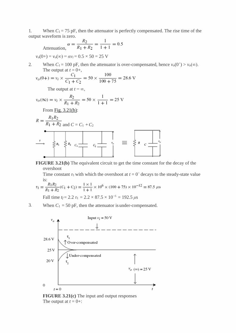
1. When C1 = 75 pF, then the attenuator is perfectly compensated. The rise time of the
output waveform is zero.
Attenuation,
vo(0+) = vo(∞) = αvi = 0.5 × 50 = 25 V
2. When C1 = 100 pF, then the attenuator is over-compensated, hence vo(0+) > vo(∞).
The output at t = 0+,
The output at t = ∞,
From Fig. 3.21(b):
and C = C1 + C2
FIGURE 3.21(b) The equivalent circuit to get the time constant for the decay of the
overshoot
Time constant τ1 with which the overshoot at t = 0+ decays to the steady-state value
is:
Fall time tf = 2.2 τ1 = 2.2 × 87.5 × 10−6 = 192.5 μs
3. When C1 = 50 pF, then the attenuator is under-compensated.
FIGURE 3.21(c) The input and output responses
The output at t = 0+:

The output at t = ∞:
The time constant, τ2, with which the output rises to the steady-state value is:
Rise time, tr = 2.2 τ2
tr = 2.2 × 62.5 × 10−6 = 137.5 μs
RLC CIRCUITS
RLC circuits behave altogether differently when compared to either RL or RC circuits. RLC
circuits are resonant circuits. These can be either series resonant circuits or parallel
resonant circuits. A parallel RLC circuit is used as a tank circuit in an oscillator to generate
oscillations (this is the feedback network that produces the phase shift of 180°). The RLC
circuit is also used in tuned amplifiers to select a desired frequency band at the output.
When a sinusoidal signal is applied as input to a series RLC circuit [see Fig. 3.23(a)], the
frequency-vs-current characteristic is as shown in Fig. 3.23(b).
At resonance: XL = XC
FIGURE 3.23(a) An RLC series circuit with sinusoidal input; (b) the frequency-vs-current
characteristic

FIGURE 3.23(c) A parallel RLC resonant circuit with sinusoidal input; (d) the frequency-
vs- voltage characteristic
At resonance, the impedance is minimum, purely resistive and equal to R. The current at the
resonant frequency, fo is maximum, termed imax. Let us now consider a parallel resonant circuit
[see Fig. 3.23(c)] and its frequency-vs-vo characteristic, shown in Fig. 3.23(d). In the parallel
resonant circuit, the impedance is maximum at resonance and hence, the voltage is maximum
at fo. The figure of merit of a tuned circuit, denoted by Q, is given as:
The larger the value of Q, the sharper the response characteristic of the tuned circuit.
The Response of the RLC Parallel Circuit to a Step Input
Consider the RLC circuit shown in Fig. 3.24(a). Applying Laplace transforms, the above circuit
is redrawn shown in Fig. 3.24(b). The impedance of the parallel combination of Ls and 1/Cs is:
FIGURE 3.24(a) RLC parallel circuit

FIGURE 3.24(b) The Laplace circuit of Fig. 3.24(a)
Multiplying the numerator and denominator by Cs we get:
Therefore,
The characteristic equation is:
The roots of this characteristic equation are:
Let K, the damping constant, be given by:
From Eq. (3.51), the resonant frequency of the tank circuit is:
From Eqs. (3.56) and (3.57):

Therefore,
Putting Eq. (3.58) in Eq.
(3.55): Therefore,
From Eq. (3.56) we have:
Therefore,
From Eq. (3.53):
For unit step voltage as input:
Applying partial fractions:
Putting s = s1
Putting s = s2

Applying inverse Laplace transform to both sides, we get:
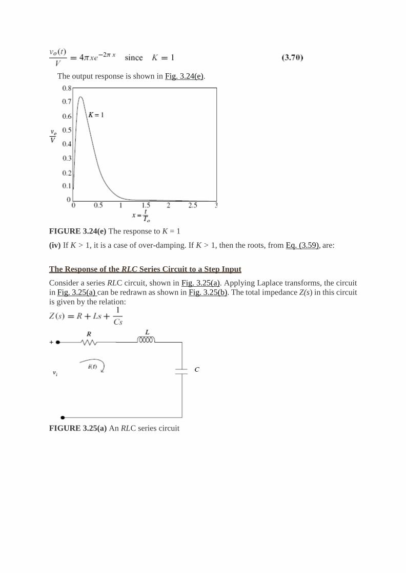
From Eq. (3.59):
(i) If K = 0:
Using Eq. (3.60):
Let
Therefore,
If we substitute the value of To from Eq. (3.57) in Eq. (3.65):
Thus, K → 0, as R → ∞. Here, K can not be zero as assumed ideally, since R = ∞ means
open-circuiting the resistance R in the circuit shown in Fig. 3.24(a), which is absurd because
the excitation is not connected to the circuit when R = ∞. However, R can be made very large,
in which case K becomes very small, though not zero as expected. The output has a smaller
amplitude but is oscillatory in nature, as seen from Eq. (3.66). Thus, when a step is applied as
input to the RLC circuit in Fig. 3.24(a), with K = 0 (practically very small), the response is un-
damped oscillations, as shown in Fig. 3.24(c).

FIGURE 3.24(c) The response to K = 0
(ii) If K < 1, it is a case of under-damping as shown in Fig. 3.24(d). For this condition, from Eq.
(3.59):
Therefore,
Multiply and divide Eq. (3.67) by K and substitute K/To = 1/4πRC in it. The resultant
equation is:
From Eq. (3.60):
where

The output response is an under-damped sinusoidal waveform. The oscillations die down
after a few cycles, as shown in Fig. 3.24(d).
FIGURE 3.24(d) The response to K < 1
(iii) If K = 1, it is a case of critical damping. If we substitute the K value in the Eq. (3.59), then
the roots are s1 = s2 = −2π/To. The roots are equal and real.
If the input is a step voltage:
Here,
Therefore,
Applying inverse Laplace transform on both sides:
where x = t/To:
Here:
The output response is shown in Fig. 3.24(e).
FIGURE 3.24(e) The response to K = 1
(iv) If K > 1, it is a case of over-damping. If K > 1, then the roots, from Eq. (3.59), are:
The Response of the RLC Series Circuit to a Step Input
Consider a series RLC circuit, shown in Fig. 3.25(a). Applying Laplace transforms, the circuit
in Fig. 3.25(a) can be redrawn as shown in Fig. 3.25(b). The total impedance Z(s) in this circuit
is given by the relation:
FIGURE 3.25(a) An RLC series circuit

FIGURE 3.25(b) The Laplace circuit of Fig. 3.25(a)
Therefore,
But
Substituting Eq. (3.77) in Eq. (3.76):
For a step input V, from Eq. 3.75
The characteristic equation is:
The roots of this characteristic equation are:

1. If either (R/2L)2 > 1/LC or R > , then both the roots are real and different, the
circuit is over-damped.
2. If either (R/2L)2 = 1/LC or R = , then both the roots are real and equal, the
circuit is critically damped.
3. If either (R/2L)2 < 1/LC or R < , then both the roots are complex conjugate to
each other; the circuit is under-damped.