Understanding the Fundamental Principles of Vector...
15
Understanding the Fundamental Principles of Vector Network Analysis Application Note
Transcript of Understanding the Fundamental Principles of Vector...

Understanding the Fundamental Principles ofVector Network Analysis
Application Note

2
Table of Contents
Introduction ....................................................................................................... 3
Measurements in Communications Systems ............................................. 3
Importance of Vector Measurements .......................................................... 5
The Basis of Incident and Reflected Power ................................................ 6
The Smith Chart ............................................................................................... 6
Power Transfer Conditions ............................................................................. 7
Network Analysis Terminology ...................................................................... 10
Measuring Group Delay .................................................................................. 12
Network Characterization............................................................................... 13
Related Literature ............................................................................................ 15
3
Introduction
Network analysis is the process by which designers and manufacturers measure
the electrical performance of the components and circuits used in more complex
systems. When these systems are conveying signals with information content,
we are most concerned with getting the signal from one point to another with
maximum efficiency and minimum distortion. Vector network analysis is a
method of accurately characterizing such components by measuring their effect
on the amplitude and phase of swept-frequency and swept-power test signals.
In this application note, the fundamental principles of vector network analysis
will be reviewed. The discussion includes the common parameters that can be
measured, including the concept of scattering parameters (S-parameters). RF fun-
damentals such as transmission lines and the Smith chart will also be reviewed.
Agilent Technologies offers a wide range of portable and benchtop vector
network analyzers for characterizing components from DC to 110 GHz. These
instruments are available with a wide range of options to simplify testing in the
field, laboratory, and production environments.
Measurements in Communications Systems
In any communications system, the effect of signal distortion must be consid-
ered. While we generally think of the distortion caused by nonlinear effects
(for example, when intermodulation products are produced from desired carrier
signals), purely linear systems can also introduce signal distortion. Linear
systems can change the time waveform of signals passing through them by
altering the amplitude or phase relationships of the spectral components that
make up the signal.
Let’s examine the difference between linear and nonlinear behavior more closely.
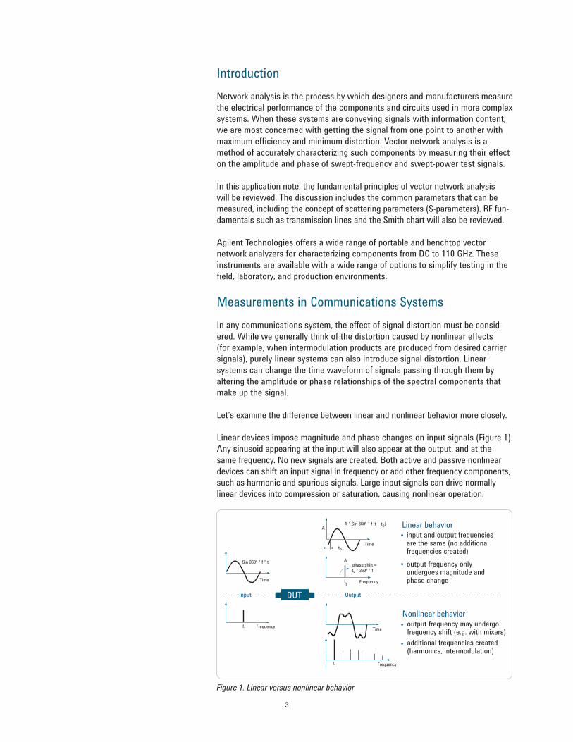
Linear devices impose magnitude and phase changes on input signals (Figure 1).
Any sinusoid appearing at the input will also appear at the output, and at the
same frequency. No new signals are created. Both active and passive nonlinear
devices can shift an input signal in frequency or add other frequency components,
such as harmonic and spurious signals. Large input signals can drive normally
linear devices into compression or saturation, causing nonlinear operation.
Linear behaviorinput and output frequencies are the same (no additional frequencies created)
output frequency only undergoes magnitude and phase change
Time
A
to
Frequencyf1
Time
Sin 360º * f * t
Frequency
A phase shift = to * 360º * f
1f
DUT
A * Sin 360º * f (t – to)
Input Output
Time
Frequency
Nonlinear behavioroutput frequency may undergo frequency shift (e.g. with mixers)
additional frequencies created (harmonics, intermodulation)
f1
Figure 1. Linear versus nonlinear behavior

4
For linear distortion-free transmission, the amplitude response of the device
under test (DUT) must be flat and the phase response must be linear over the
desired bandwidth. As an example, consider a square-wave signal rich in high-
frequency components passing through a bandpass filter that passes selected
frequencies with little attenuation while attenuating frequencies outside of the
passband by varying amounts.
Even if the filter has linear phase performance, the out-of-band components
of the square wave will be attenuated, leaving an output signal that, in this
example, is more sinusoidal in nature (Figure 2).
If the same square-wave input signal is passed through a filter that only inverts
the phase of the third harmonic, but leaves the harmonic amplitudes the same,
the output will be more impulse-like in nature (Figure 3). While this is true for
the example filter, in general, the output waveform will appear with arbitrary
distortion, depending on the amplitude and phase nonlinearities.
Frequency FrequencyFrequency
Mag
nit
ude
Time
Linear network
Time
F(t) = sin wt + 1/3 sin 3wt + 1/5 sin 5wt
Figure 2. Magnitude variation with frequency
Frequency
Mag
nit
ude
Linear network
Frequency
Frequency
Time
0º
–360º
–180º
Time
F(t) = sin wt + 1/3 sin 3wt + 1/5 sin 5wt
Figure 3. Phase variation with frequency

5
Figure 4. Nonlinear induced distortion
Nonlinear devices also introduce distortion (Figure 4). For example, if an ampli-
fier is overdriven, the output signal clips because the amplifier is saturated.
The output signal is no longer a pure sinusoid, and harmonics are present at
multiples of the input frequency. Passive devices may also exhibit nonlinear
behavior at high power levels, a good example of which is an L-C filter that uses
inductors with magnetic cores. Magnetic materials often exhibit hysteresis
effects that are highly nonlinear.
Efficient transfer of power is another fundamental concern in communications
systems. In order to efficiently convey, transmit or receive RF power, devices
such as transmissions lines, antennas and amplifiers must present the proper
impedance match to the signal source. Impedance mismatches occur when the
real and imaginary parts of input and output impedances are not ideal between
two connecting devices.
Importance of Vector Measurements
Measuring both magnitude and phase of components is important for several
reasons. First, both measurements are required to fully characterize a linear
network and ensure distortion-free transmission. To design efficient matching
networks, complex impedance must be measured. Engineers developing models
for computer-aided-engineering (CAE) circuit simulation programs require
magnitude and phase data for accurate models.
In addition, time-domain characterization requires magnitude and phase
information in order to perform an inverse-fourier transform. Vector error
correction, which improves measurement accuracy by removing the effects
of inherent measurement-system errors, requires both magnitude and phase
data to build an effective error model. Phase-measurement capability is very
important even for scalar measurements such as return loss, in order to achieve
a high level of accuracy (see Applying Error Correction to Network Analyzer
Measurements, Agilent application note 1287-3).
Nonlinear networks
Frequency Frequency
TimeTime
Saturation, crossover, intermodulation, and other nonlinear effects can cause signal distortion
6
The Basis of Incident and Refl ected Power
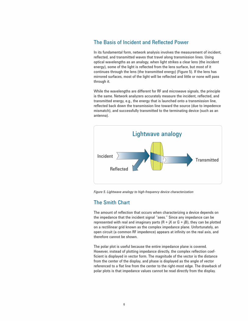
In its fundamental form, network analysis involves the measurement of incident,
reflected, and transmitted waves that travel along transmission lines. Using
optical wavelengths as an analogy, when light strikes a clear lens (the incident
energy), some of the light is reflected from the lens surface, but most of it
continues through the lens (the transmitted energy) (Figure 5). If the lens has
mirrored surfaces, most of the light will be reflected and little or none will pass
through it.
While the wavelengths are different for RF and microwave signals, the principle
is the same. Network analyzers accurately measure the incident, reflected, and
transmitted energy, e.g., the energy that is launched onto a transmission line,
reflected back down the transmission line toward the source (due to impedence
mismatch), and successfully transmitted to the terminating device (such as an
antenna).
Figure 5. Lightwave analogy to high-frequency device characterization
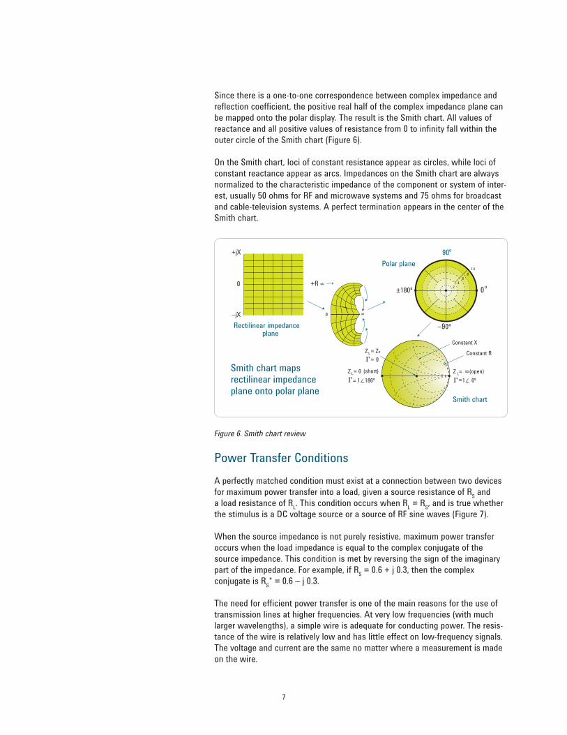
The Smith Chart
The amount of reflection that occurs when characterizing a device depends on
the impedance that the incident signal “sees.” Since any impedance can be
represented with real and imaginary parts (R + jX or G + jB), they can be plotted
on a rectilinear grid known as the complex impedance plane. Unfortunately, an
open circuit (a common RF impedence) appears at infinity on the real axis, and
therefore cannot be shown.
The polar plot is useful because the entire impedance plane is covered.
However, instead of plotting impedance directly, the complex reflection coef-
ficient is displayed in vector form. The magnitude of the vector is the distance
from the center of the display, and phase is displayed as the angle of vector
referenced to a flat line from the center to the right-most edge. The drawback of
polar plots is that impedance values cannot be read directly from the display.
Incident
Reflected
Transmitted
Lightwave analogy
7
Since there is a one-to-one correspondence between complex impedance and
reflection coefficient, the positive real half of the complex impedance plane can
be mapped onto the polar display. The result is the Smith chart. All values of
reactance and all positive values of resistance from 0 to infinity fall within the
outer circle of the Smith chart (Figure 6).
On the Smith chart, loci of constant resistance appear as circles, while loci of
constant reactance appear as arcs. Impedances on the Smith chart are always
normalized to the characteristic impedance of the component or system of inter-
est, usually 50 ohms for RF and microwave systems and 75 ohms for broadcast
and cable-television systems. A perfect termination appears in the center of the
Smith chart.
Figure 6. Smith chart review
Power Transfer Conditions
A perfectly matched condition must exist at a connection between two devices
for maximum power transfer into a load, given a source resistance of RS and
a load resistance of RL. This condition occurs when R
L = R
S, and is true whether
the stimulus is a DC voltage source or a source of RF sine waves (Figure 7).
When the source impedance is not purely resistive, maximum power transfer
occurs when the load impedance is equal to the complex conjugate of the
source impedance. This condition is met by reversing the sign of the imaginary
part of the impedance. For example, if RS = 0.6 + j 0.3, then the complex
conjugate is RS* = 0.6 – j 0.3.
The need for efficient power transfer is one of the main reasons for the use of
transmission lines at higher frequencies. At very low frequencies (with much
larger wavelengths), a simple wire is adequate for conducting power. The resis-
tance of the wire is relatively low and has little effect on low-frequency signals.
The voltage and current are the same no matter where a measurement is made
on the wire.
–90º
0o
±180º.2
.4
.6
.8
1.0
90o
0
0 +R
+jX
–jX
$
Smith chart maps rectilinear impedance plane onto polar plane
Rectilinear impedance plane
Polar plane
Z = ZoL
= 0G
Constant X
Constant R
Z = L
=1_ 0ºG
Smith chart
$(open)
GLZ = 0
= 1_180º
(short)
$

8
At higher frequencies, wavelengths are comparable to or smaller than the
length of the conductors in a high-frequency circuit, and power transmission
can be thought of in terms of traveling waves. When the transmission line is
terminated in its characteristic impedance, maximum power is transferred to the
load. When the termination is not equal to the characteristic impedance, that
part of the signal that is not absorbed by the load is reflected back to
the source.
If a transmission line is terminated in its characteristic impedance, no reflected
signal occurs since all of the transmitted power is absorbed by the load (Figure 8).
Looking at the envelope of the RF signal versus distance along the transmission
line shows no standing waves because without reflections, energy flows in only
one direction.
0 1 2 3 4 5 6 7 8 9 100
0.2
0.4
0.6
0.8
1
1.2
Load
pow
er (
norm
aliz
ed)
RL / RS
RS
RL
Maximum power is transferred when RL = RS
For complex impedances, maximum power transfer occurs when ZL = ZS* (conjugate match)
Zs = R + jX
ZL = Zs* = R – jX
Figure 7. Power transfer
For reflection, a transmission line terminated in Zo behaves like an infinitely long transmission line
Zs = Zo
Zo
Vrefl = 0 (all the incident power is absorbed in the load)
Vinc
Zo = characteristic impedance of transmission line
Figure 8. Transmission line terminated with Z0

9
When the transmission line is terminated in a short circuit (which can sustain
no voltage and therefore dissipates zero power), a reflected wave is launched
back along the line toward the source (Figure 9). The reflected voltage wave
must be equal in magnitude to the incident voltage wave and be 180 degrees
out of phase with it at the plane of the load. The reflected and incident waves
are equal in magnitude but traveling in the opposite directions.
If the transmission line is terminated in an open-circuit condition (which can
sustain no current), the reflected current wave will be 180 degrees out of phase
with the incident current wave, while the reflected voltage wave will be in phase
with the incident voltage wave at the plane of the load. This guarantees that the
current at the open will be zero. The reflected and incident current waves are
equal in magnitude, but traveling in the opposite directions. For both the short
and open cases, a standing wave pattern is set up on the transmission line.
The voltage valleys will be zero and the voltage peaks will be twice the incident
voltage level.
If the transmission line is terminated with say a 25-ohm resistor, resulting in
a condition between full absorption and full reflection, part of the incident power
is absorbed and part is reflected. The amplitude of the reflected voltage wave will
be one-third that of the incident wave, and the two waves will be 180 degrees out
of phase at the plane of the load. The valleys of the standing-wave pattern will no
longer be zero, and the peaks will be less than those of the short and open cases.
The ratio of the peaks to valleys will be 2:1.
The traditional way of determining RF impedance was to measure VSWR using an
RF probe/detector, a length of slotted transmission line, and a VSWR meter. As
the probe was moved along the transmission line, the relative position and values
of the peaks and valleys were noted on the meter. From these measurements,
impedance could be derived. The procedure was repeated at different frequencies.
Modern network analyzers measure the incident and reflected waves directly
during a frequency sweep, and impedance results can be displayed in any number
of formats (including VSWR).
Zs = Zo
Vrefl
Vinc
For reflection, a transmission line terminated ina short or open reflects all power back to source
In phase (0º) for open
Out of phase (180º) for short
Figure 9. Transmission line terminated with short, open
10
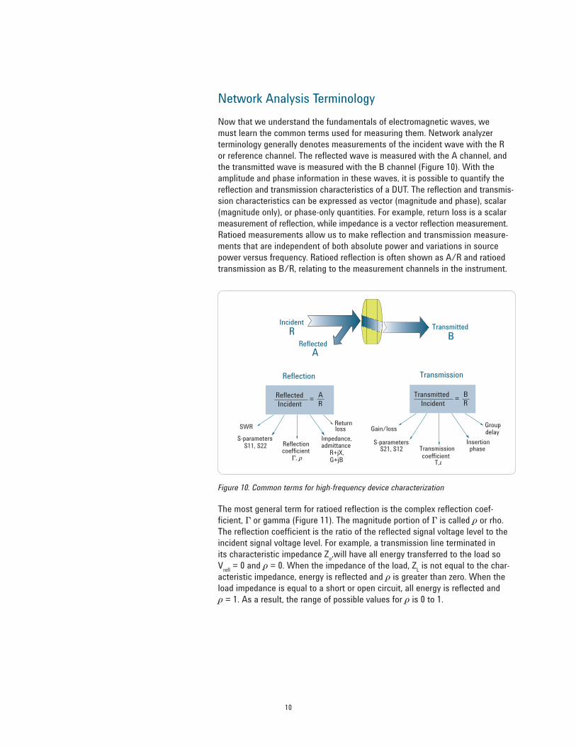
Network Analysis Terminology
Now that we understand the fundamentals of electromagnetic waves, we
must learn the common terms used for measuring them. Network analyzer
terminology generally denotes measurements of the incident wave with the R
or reference channel. The reflected wave is measured with the A channel, and
the transmitted wave is measured with the B channel (Figure 10). With the
amplitude and phase information in these waves, it is possible to quantify the
reflection and transmission characteristics of a DUT. The reflection and transmis-
sion characteristics can be expressed as vector (magnitude and phase), scalar
(magnitude only), or phase-only quantities. For example, return loss is a scalar
measurement of reflection, while impedance is a vector reflection measurement.
Ratioed measurements allow us to make reflection and transmission measure-
ments that are independent of both absolute power and variations in source
power versus frequency. Ratioed reflection is often shown as A/R and ratioed
transmission as B/R, relating to the measurement channels in the instrument.
Figure 10. Common terms for high-frequency device characterization
The most general term for ratioed reflection is the complex reflection coef-
ficient, G or gamma (Figure 11). The magnitude portion of G is called r or rho.
The reflection coefficient is the ratio of the reflected signal voltage level to the
incident signal voltage level. For example, a transmission line terminated in
its characteristic impedance Zo,will have all energy transferred to the load so
Vrefl
= 0 and r = 0. When the impedance of the load, ZL is not equal to the char-
acteristic impedance, energy is reflected and r is greater than zero. When the
load impedance is equal to a short or open circuit, all energy is reflected and
r = 1. As a result, the range of possible values for r is 0 to 1.
Transmission
Gain/loss
S-parametersS21, S12
Groupdelay
Transmissioncoefficient
Insertion phase
Reflection
SWR
S-parametersS11, S22 Reflection
coefficient
Impedance, admittance
R+jX, G+jB
Returnloss
G, rT,t
Incident
Reflected
TransmittedR B
A
ReflectedIncident
AR
=Transmitted
Incident
BR
=

11
Figure 11. Refl ection parameters
Return loss is a way to express the reflection coefficient in logarithmic terms
(decibels). Return loss is the number of decibels that the reflected signal is
below the incident signal. Return loss is always expressed as a positive number
and varies between infinity for a load at the characteristic impedance and 0 dB
for an open or short circuit. Another common term used to express reflection is
voltage standing wave ratio (VSWR), which is defined as the maximum value of
the RF envelope over the minimum value of the RF envelope. It is related to r as
(1 + r)/(1 – r). VSWR ranges from 1 (no reflection) to infinity (full reflection).
The transmission coefficient is defined as the transmitted voltage divided by
the incident voltage (Figure 12). If the absolute value of the transmitted voltage
is greater than the absolute value of the incident voltage, a DUT or system is
said to have gain. If the absolute value of the transmitted voltage is less than
the absolute value of the incident voltage, the DUT or system is said to have
attenuation or insertion loss. The phase portion of the transmission coefficient
is called insertion phase.
=Z
L- Z O
ZL + OZ
Reflectioncoefficient
=Vreflected
Vincident
= r FG
=r G
$ dB
No reflection(ZL = Zo)
rRL
VSWR
0 1
Full reflection(ZL = open, short)
0 dB
1 $
Return loss = –20 log(r),
VSWR = Emax
Emin=
1 + r1 – r
Voltage standing wave ratioEmax
Emin
VTransmittedVIncident
Transmission coefficient = T =VTransmitted
VIncident
= t _ f
DUT
Gain (dB) = 20 Log V
Trans
VInc
= 20 log t
Insertion loss (dB) = –20 Log V
Trans
VInc
= –20 log t
Figure 12. Transmission parameters
12
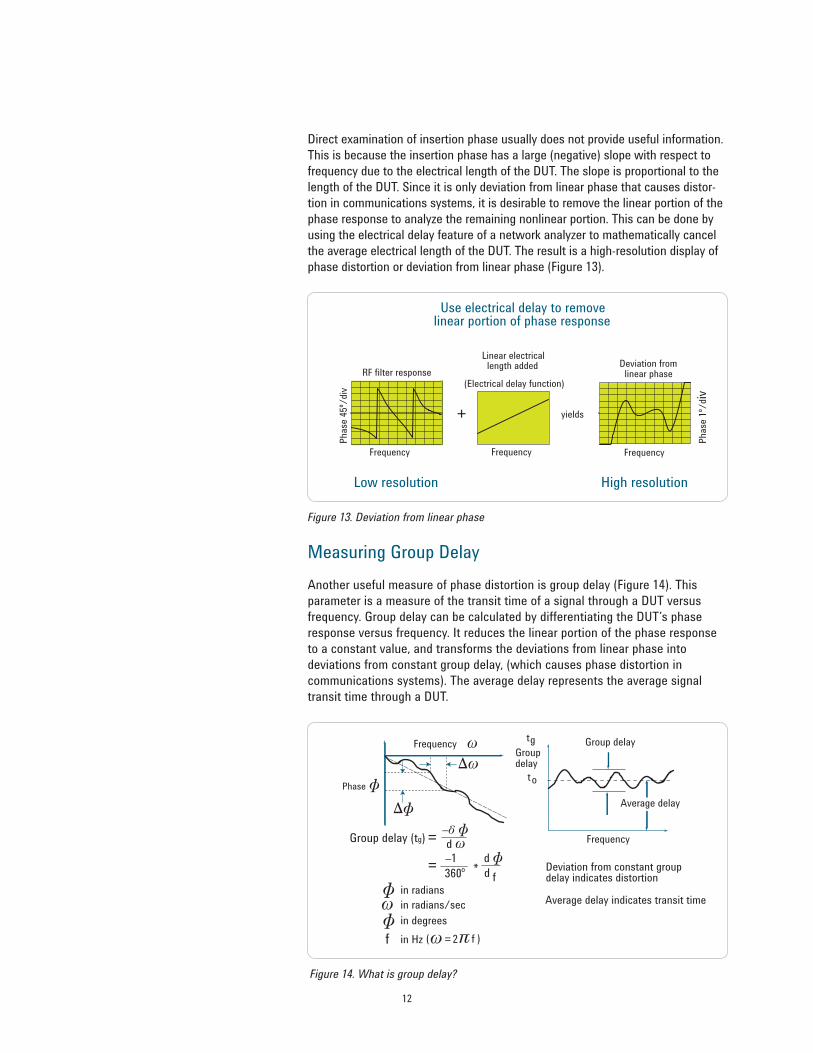
Direct examination of insertion phase usually does not provide useful information.
This is because the insertion phase has a large (negative) slope with respect to
frequency due to the electrical length of the DUT. The slope is proportional to the
length of the DUT. Since it is only deviation from linear phase that causes distor-
tion in communications systems, it is desirable to remove the linear portion of the
phase response to analyze the remaining nonlinear portion. This can be done by
using the electrical delay feature of a network analyzer to mathematically cancel
the average electrical length of the DUT. The result is a high-resolution display of
phase distortion or deviation from linear phase (Figure 13).
Figure 13. Deviation from linear phase
Measuring Group Delay
Another useful measure of phase distortion is group delay (Figure 14). This
parameter is a measure of the transit time of a signal through a DUT versus
frequency. Group delay can be calculated by differentiating the DUT’s phase
response versus frequency. It reduces the linear portion of the phase response
to a constant value, and transforms the deviations from linear phase into
deviations from constant group delay, (which causes phase distortion in
communications systems). The average delay represents the average signal
transit time through a DUT.
Use electrical delay to remove linear portion of phase response
Linear electrical length added
+ yields
Frequency
(Electrical delay function)
Frequency
RF filter responseDeviation from linear phase
Phas
e 1º
/di
v
Phas
e 45
º/di
v
Frequency
Low resolution High resolution
Deviation from constant group delay indicates distortion
Average delay indicates transit time
Groupdelay
Frequency
Group delay
Average delay
to
tg
Group delay (tg)
=–1
360o
=–d fd w
d fd f
in radians
in radians/sec
in degrees
in Hzf
fwf
2=( )fw p
Phase f
Df
*
DwFrequency w
Figure 14. What is group delay?

13
Depending on the device, both deviation from linear phase and group delay may
be measured, since both can be important. Specifying a maximum peak-to-peak
phase ripple in a device may not be sufficient to completely characterize it, since
the slope of the phase ripple depends on the number of ripples that occur per
unit of frequency. Group delay takes this into account because it is the differen-
tiated phase response. Group delay is often a more easily interpreted indication
of phase distortion (Figure 15).
Figure 15. Why measure group delay?
Network Characterization
In order to completely characterize an unknown linear two-port device, we must
make measurements under various conditions and compute a set of parameters.
These parameters can be used to completely describe the electrical behavior of
our device (or network), even under source and load conditions other than when
we made our measurements. Low-frequency device or network characterization
is usually based on measurement of H, Y, and Z parameters. To do this, the
total voltage and current at the input or output ports of a device or nodes of a
network must be measured. Furthermore, measurements must be made with
open-circuit and short-circuit conditions.
Since it is difficult to measure total current or voltage at higher frequencies,
S-parameters are generally measured instead (Figure 16). These parameters
relate to familiar measurements such as gain, loss, and reflection coefficient.
They are relatively simple to measure, and do not require connection of
undesirable loads to the DUT. The measured S-parameters of multiple devices
can be cascaded to predict overall system performance. S-parameters are read-
ily used in both linear and nonlinear CAE circuit simulation tools, and H, Y, and Z
parameters can be derived from S-parameters when necessary.
The number of S-parameters for a given device is equal to the square of the
number of ports. For example, a two-port device has four S-parameters. The
numbering convention for S-parameters is that the first number following the
S is the port at which energy emerges, and the second number is the port at
which energy enters. So S21
is a measure of power emerging from Port 2 as a
result of applying an RF stimulus to Port 1. When the numbers are the same
(e.g. S11
), a reflection measurement is indicated.
Same peak-to-peak phase ripple can result in different group delay
Phas
e
Phas
e
Gro
up
dela
y
Gro
up
dela
y
f
f
f
f
–dφdw
–dφdw
14
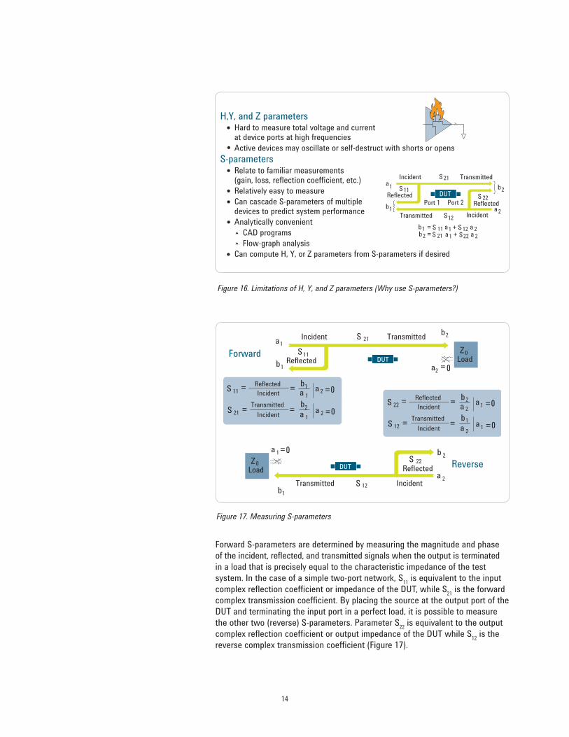
Forward S-parameters are determined by measuring the magnitude and phase
of the incident, reflected, and transmitted signals when the output is terminated
in a load that is precisely equal to the characteristic impedance of the test
system. In the case of a simple two-port network, S11
is equivalent to the input
complex reflection coefficient or impedance of the DUT, while S21
is the forward
complex transmission coefficient. By placing the source at the output port of the
DUT and terminating the input port in a perfect load, it is possible to measure
the other two (reverse) S-parameters. Parameter S22
is equivalent to the output
complex reflection coefficient or output impedance of the DUT while S12
is the
reverse complex transmission coefficient (Figure 17).
H,Y, and Z parametersHard to measure total voltage and current at device ports at high frequencies
Active devices may oscillate or self-destruct with shorts or opens
S-parametersRelate to familiar measurements (gain, loss, reflection coefficient, etc.)
Relatively easy to measure
Can cascade S-parameters of multiple devices to predict system performance
Analytically convenient
CAD programs
Flow-graph analysis
Can compute H, Y, or Z parameters from S-parameters if desired
Incident TransmittedS 21
S 11Reflected S 22
Reflected
Transmitted Incident
b1
a1 b2
a 2S12
DUT
b1 = S 11 a1 + S 12 a 2b2 = S 21 a1 + S22 a 2
Port 1 Port 2
Figure 16. Limitations of H, Y, and Z parameters (Why use S-parameters?)
S 11 =Reflected
Incident=
b1
a 1a 2 =0
S 21 =Transmitted
Incident=
b2
a 1a 2 =0
21
1
2
1
Incident TransmittedS 21
S 11Reflectedb1
a1
b2
Z0
Loada2
=0DUT
DUT
Forward
IncidentTransmitted S 12
S 22
Reflected
b 2
a 2
1b
a 1 =0
Z0
LoadReverse
S 22 =Reflected
Incident=
ba a =0
S 12 =Transmitted
Incident=
b
2a a =0
Figure 17. Measuring S-parameters

For more information on Agilent Technologies’ products, applications or services, please contact your local Agilent
office. The complete list is available at:
www.agilent.com/fi nd/contactus
AmericasCanada (877) 894 4414 Brazil (11) 4197 3600Mexico 01800 5064 800 United States (800) 829 4444
Asia Pacifi cAustralia 1 800 629 485China 800 810 0189Hong Kong 800 938 693India 1 800 112 929Japan 0120 (421) 345Korea 080 769 0800Malaysia 1 800 888 848Singapore 1 800 375 8100Taiwan 0800 047 866Other AP Countries (65) 375 8100
Europe & Middle EastBelgium 32 (0) 2 404 93 40 Denmark 45 45 80 12 15Finland 358 (0) 10 855 2100France 0825 010 700* *0.125 €/minute
Germany 49 (0) 7031 464 6333 Ireland 1890 924 204Israel 972-3-9288-504/544Italy 39 02 92 60 8484Netherlands 31 (0) 20 547 2111Spain 34 (91) 631 3300Sweden 0200-88 22 55United Kingdom 44 (0) 118 927 6201
For other unlisted countries: www.agilent.com/fi nd/contactusRevised: January 6, 2012
Product specifications and descriptions in this document subject to change without notice.
© Agilent Technologies, Inc. 2012Published in USA, September 7, 20125965-7707E
www.agilent.comwww.agilent.com/find/NA
Agilent Advantage Services is committed
to your success throughout your equip-
ment’s lifetime. To keep you competitive,
we continually invest in tools and
processes that speed up calibration and
repair and reduce your cost of ownership.
You can also use Infoline Web Services
to manage equipment and services more
effectively. By sharing our measurement
and service expertise, we help you create
the products that change our world.
www.agilent.com/find/advantageservices
Agilent Email Updates
www.agilent.com/find/emailupdatesGet the latest information on the
products and applications you select.
www.agilent.com/qualityQuality Management SystemQuality Management Sys
ISO 9001:2008Agilent Electronic Measurement Group
DEKRA Certified
Related Literature
Exploring the Architectures of Network
Analyzers, Application Note 1287-2,
Literature number 5965-7708E
Applying Error Correction to
Network Analyzer Measurements,
Application Note 1287-3,
Literature number 5965-7709E
Network Analyzer Measurements:
Filter and Amplifier Examples,
Application Note 1287-4,
Literature number 5965-7710E