UNCLASSIFIED AD NUMBER - Defense Technical Information Center UNCLASSIFIED AD NUMBER AD911513 NEW...
82
UNCLASSIFIED AD NUMBER AD911513 NEW LIMITATION CHANGE TO Approved for public release, distribution unlimited FROM Distribution authorized to U.S. Gov't. agencies only; Test and Evaluation; APR 1973. Other requests shall be referred to Air Force Avionics Laboratory, Attn: TEM, Wright-Patterson AFB, OH 45433. AUTHORITY AFAL ltr, 3 Feb 1976 THIS PAGE IS UNCLASSIFIED
-
Upload
vuongduong -
Category
Documents
-
view
223 -
download
2
Transcript of UNCLASSIFIED AD NUMBER - Defense Technical Information Center UNCLASSIFIED AD NUMBER AD911513 NEW...

UNCLASSIFIED
AD NUMBER
AD911513
NEW LIMITATION CHANGE
TOApproved for public release, distributionunlimited
FROMDistribution authorized to U.S. Gov't.agencies only; Test and Evaluation; APR1973. Other requests shall be referred toAir Force Avionics Laboratory, Attn: TEM,Wright-Patterson AFB, OH 45433.
AUTHORITY
AFAL ltr, 3 Feb 1976
THIS PAGE IS UNCLASSIFIED

AFAL-TR-73-72 4
MICROWAVE FILTERS AND DELAY LINES
W. L. Bongianni, D. M. Heinz and L. Needham
Electronics Group of North American Rockwell
TECHNICAL REPORT AFAL-TR-73- 72
plum April 1973
CDDC
"Distribution limited to US Government egencies only;
'-.-' L 3 -. test end evaluation results reported; (April 1973).
Other requests for this document must be referred to
AFAL/TEM, Wrihi-Patterion AFB, OH 45433"
Air Force Avionics Laboratory
Air Force Systems Command
Wright-Patterson Air Force Base, Ohio
Jl X l A t t ..................................
NOTICE
Wheom Govrnmont drangs, specications, or other data are Oa for amy purposeother than in conneatin with a definitely related Govewrment procurement operation,the United States Govsrament thereby incun na responsibility nor any obligationwhatoeom, and the fact that the government my haM foamulamd, furnishdl, oa inany way upplied tin aid drawnglS, spaciflations, or ether data. is not t he regardedby implication or otherwise a in any momenr licensing tie homdr or any Other parinsor corporation, or conveying any rights ow permission to manufactute, use, or all anypatented invtion that my In any way •e relted thereto.
Copies of this report should not bh returned unless return is required by securityconsiderations, contractual obligations, or notice an a specific document.
dj

-•( ~ r - % -.- ..........- 6
MICROWAVE FILTERS AND DELAY LINES,
"". WLjngianni D M14 einz I" LL.Needham
r -~- -_.. . ..-
"Distribution limited to US Government agencies only;test and evaluation results reported; (April 1973).Other requests for this document must be referred toAFAL/TEM, Wright-Patterson AFB, OH 45433"'
(/.,9,) ,/ ._/
FOREWORD
This report on contract F33615-72-C-1760 was prepared by the AdvancedDevice Technology Department under Peter J. Hagon. This department is part ofthe Physical Sciences Department in the Research and Technology Division, NorthAmerican Rockwell Electronics Group.
The contract was initiated under Project 4460, "Solid State DevelopmentTechnology," Task 446007, "Integrated Microwave Circuits," and was administeredby the Air Force Avionics Laboratory, Wright-Patterson Air Force Base, Ohio,with Mr. Russell W. Runnels (AFAL/TEM) as project engineer. The report coversthe period 8 May 1972 to 29 December 1972. The contractor's report number isC72-585/501.
The authors would like to acknowledge the significant contributions made byE. Grubb and J. E. Mee.
This report was submitted by the authors April 1973.
"Publication of this report does not constitute Air Force approval of thereport's findings or conclusions. It is published only for the exchange andstimulation of ideas".
WILLIAM J. EDWARDSChief, Radar and Microwave Technology BrElectronic Technology DivisionAir Force Avionics Laboratory
1" ii
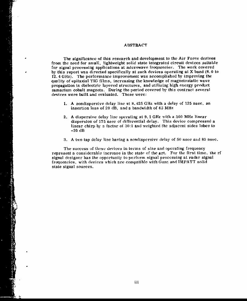
ABSTRACT
The significance of this research and development to the Air Force derivesfrom the need for small, lightweight solid state integrated circuit devices .suitablefor signal processing applications at microwave frequencies. The work coveredby this report was directed specifically at such devices operating at X band (8.0 to12. 4 GHz). The performance improvement was accomplished by improving thequality of epitaxial YIG films, increasing the knowledge of magnetostatic wavepropagation in dielectric layered structures, and utilizing high energy productsamarium cobalt magnets. During the period covered by this contract severaldevices were built and evaluated. These were:
1. A nondispersive delay line at 8.425 GHz with a delay of 125 nsec, aninsertion loss of 20 dB, and a bandwidth of 45 MHz
2. A dispersive delay line operating at 9. 1 GHz with a 300 MHz lineardispersion of 175 nsec of differential delay. This device compressed alinear chirp by a factor of 30:1 and weighted the adjacent sides lobes to-20 dB
3. A two tap delay line having a nondispersive delay of 50 nsec and 80 nsec.
The success of these devices in terms of size and operating frequencyrepresent a considerable increase in the state of the art. For the first time, the rfsignal designer has the opportunity to perform signal processing at radar signalfrequencies, with devices which are compatible with Gunn and IMPATT solidstate signal sources.
ii

CONTENTS
Section Page
I. Introduction ....................... ............ 1
1. Technical Background ............................... 22. Objectives ........................................ 2
a. YIG Film Quality ................................. 2b. Samarium Cobalt Magnets .......................... 2c. Dielectric Layered Structure ........................ 2
HI. Film Fabrication ..................................... 3
1. Background ...................................... 32. Substrates ....................................... 3
a. Bulk Imperfections in Substrate Wafers ...................... 4b. Surface Imperfections in Substrate Wafers ..................... 6
3. Epitaxial Film Growth ..................................... 7
a. Chemical Vapor Deposition ....... ......................... 7b. Liquid Phase Epitaxy ............................. 12
4. Epitaxial Film Characterization ......................... 14
III. Film Evaluation ..................................... 18
1. Magnetic Wave Propagation Ioss .......... ,.............182. Propagation Loss Measurements on Rough Films ................. 203. Epitaxial Growth Rings and Their Effect on Linewidth .............. 214. Propagation Loss on Flux Grown YIG ...................... 265. Power Saturation in Flux Grown YIG ........................... 306. Cumulative Table of Film Quality ........................ 317. Conclusions on Film Quality ........................... 31
IV, Samarium Cobalt Magnets ............................... 34
1. Pernmanent Magnet Field Strength and Field Uniformity ........... 342. Permanent Magnet Task ....... ............................. 343. General Magnet Design Considerations .......................... 344. Magnet Field Strength Measurements .......................... 35
a. Proposal Configuration - Single Magnet ..................... 35b. Single Magnet-Measured Across Poles Parallel to X-Axis ..... .. 35c. Single Magnet-Measured Across Poles Parallel Y-Axis ........ .35d. Dual Magnets - Measured Between Poles Parallel Y-Axis ...... - 39e. Dual Magnets on Laminated Silicon Iron Sub-Yoke .............. 39f. Dual Magnets on External Laminated Silicon Iron Yoke ....... 39
V
MCWlCDOW pALE MAiINQ FUILUD.S.. . .. *
CONTENTS (Cont)
Section Page
g. Dual Magnets on External 1018 Steel Yoke-Field Shaping .... 39h. Triple Magnet on External 1018 Steel Yoke-Field Variation .. 401. Cruciform Magnet Configuration .................... 40j. Triple Magnet Deliverable Device ................... 40k. Five Magnet-Twin Channel Device ................... 47
5. Machining and liandling ............................. 476. Summary ...................................... 47
V. X-Band Devices .................................... Z6
1. X-Band Nondispersive Delay Line ...................... 562. X-Band Dispersive Delay Line ........................ 633. Specifications on DDL-EY-3 .......................... 68
References ....................................... 69
vi
ILLUSTRATIONS
Figre Page
1. X-ray Diffraction Topograph and Stress Patterns in a (111)Substrate Wafer ..................................... 5
2. Iridium inclusion and Strain Pattern Revealed ina Substrate Waferby Transmitted Polarized Light with Analyzer Set at Extinction ....... 6
3. Lack of Stress Patterns Revealed in a Recent (111) Substrate Waferby Transmitted Polarized Light with Analyzer Set at Extinction ....... 7
4. YIG Film Grown on GGG Substrate Which Contained MechanicalDarnage ............................... ........... 8
5. YIG Film Grown Over Poorly Cleaned Substrate ....................... 86. Schematic of T-Shaped Reaction Chamber for CVD YIG Film Growth - - 97. Microscopic Particle on CVD YIG Film ....................... I18. Schematic of Dipping Apparatus for LPE YIG Film Growth ........... 129. Microscopic Particles on LPE YIG Film ..................... 14
10. Magnetic Domains in LPE YIG Films Showing the NormalStraight Domain Walls of Slow Growth and Curved DomainWalls of Rapid Growth .................................. 15
11. Interference Fringe Pattern of a YEG Film Showing ThicknessUniformity and Mlesas Caused by Flux Retention ................ 16
12. Equivalent Circuit of Resonant Cavity ..... .................... 1813. Surface Roughness vs Film Thickness for Low Dislocation
Density Airtron GGG .................................. 2214. Linewidth as Calculated from Propagation Loss ................. 2315. Linewidth as a Function of Mechanical Polishing on Sample
No. 2771-1 ......................................... 2416. Nomarski Interference Photomicrograph of Film After
Mechanical Polishing and Chemical Etching ................... 2517. Photomicrograph of Mechanically Polished Flux Grown
YIG Showing Included Grit (280X) .......................... 2718. Flux Grown YIG Surface after Flux Polishing for 30 Seconds
at 8600 C (28CX) ...................................... 2719. Detailed View of Surface Damage (55X) ...................... 28
S20. 90 Second Flux Polish at 860°C (280X) ...................... 2821. 150 Second Flux Polish at 860"C (280X) ...................... 2922. Detailed View of Scratch and Grit Included Free Surface (55X) ........ 2923. Film Quality ........................................ 3324. Magnet Axis Identification ............................... 3625. Measurement Probe Positions ............................ 3726. Single Magnet Measured Between Poles Parallel Y Axis ............. 3827. Dual Magnets ....................................... 3928. Area for Required Field Uniformity ......................... 4029. Effects of Field Shaping in Short Direction .................... 4130. Effect of Adding Third Magnet ............................ 4231. Field Variations in Y-Axis ............................... 43.32. Cruciform Magnet Configuration ...........................33. Cruciform Magnet Support .... ........................... 4534. Triple Magnet Deliverable Device .......................... 4635. Five Magnet-Twin Chan.iel Device . ........................ 4836. Magnet Structure for Five Magnet Twin Channel Device ............ 51
vii

ILLUSTRATIONS (Cont)
Figure Page
37. Microstrip Circuit on 20 Mil Alumina ...................... 5638. 30 Mil YIG Feed 4.5 cm of Air Line ....................... 5739. 30 Mil Feed with No. 2771-3(2) YIG and 4. 5 cm Air Line ........... 5840. No. 2771-(2) YIG 3 Mil Coupler, 0.5 cm Spaling, 20 Mit Alumina .... .6041. No. 2771-3(3) YIG ..................................... 6142. No. 2771-3(3) YIG, 3 Mil Coupler, 0.5 cm Spaling,
20 Mil Alumina, (Rubber Grommet Feedthrough Suppression) ....... 6243. Dispersive Delay Line Using LPE YIG 10.28 lm Thick (NRA 403B-3) • 6444. Compression Loop for the X-Band Epitaxial YIG
Dispersive Delay Line DDL-EY-3 ......................... 6545. Spectrum of Input Chip .................... ........... 6646. Time Domain ...................................... 6647. Side Lobe Level .................................... 6748. -4 DB Points ...................................... 6749. Chip Spectrum Weighted by the Dispersive Delay Line .............. 68
"viii

TAB LES
Table Page
SI. Typical Conditions for the Chemical Vapor Deposition ofan Epitaxial YIG Film ................................. 9
II. Typical Conditions for Liquid Phase Epitaxy of an EpitaxialYIG Film ....................... . . .. .. 13
III. Comparison of Properties of YIG Films Grown on Coredand Core Free CGG Substrates ........................... -. 26
IV. YIG Sample Measured During Contract ...................... 32V. Comparison of Various Magnet Configurations ................ 55
VI. Two 10.5 Films at X-Band ............................ 59VII. Specifications on DDL-EY-3 ............................ 68
,ix
-I.

SECTION I
INTRODUCTION
1. TECHNICAL BACKGROUND
This program is a logical continuation of previous work carried out byNorth American Rockwell Corporation on ARPA and AFAL programs over the past5 years.
Techniques for epitaxial growth of single crystal yttrium iron garnet (YIG) onnonmagnetic substrates by chemical vapor deposition (CVD) were developed underARPA Order 807, contract AF33(615)-5244, June 1966-June 1968. This programalso resulted in a preliminary theoretical understanding of magnetostatic mode spectrain YIG films with experimental verification.
Work performed on a follow-on program - F33615-69-C-1520, March 1969 toJuly 1970 - extended this work. Material quality of the films was improved to thepoint where measured linewidths ('emonstrated it was comparable to the best bulkmaterial. Significant advances were made in the theory of ferromagnetic resonanceand the identification and the control of the resonance modes in the epitaxial films.Device feasibility demonstrations were successfully carried out with the resultsindicating that a powerful signal processing technology at microwave frequencies(I to 10 GHz) may result from the epitaxial YIG film approach.
Actual device fabrication was achieved in July 1969 to March 1970 whenbandpass and bandsectioning filters were delivered to MIT-Lincoln Labs. Thesefilters were built with l3w linewidth epitaxial YIG on microstrip substrates under acontract with Lincoln Labs. The performance of these devices was comparable withthat achieved in commercial YIG sphere filters.
Signal processing devices were built at S band (2 to 4 GHz) on contractF33615-71-C-1101 during the period 15 November 1970 to 15 July 1971. During thisperiod the use of thin YIG films in a dielectric layered structure was first described.Devices using this mode'of propagation consisted of a dispersive delay line and anondispersive tapped line.
2. OBJECTIVES
The purpose of this program was to obtain microwave signal processing devicesusing epitaxial YIG films at X band (8. 0 to 12.4 GHz). This was to be achieved by:(1) improving the quality of epitaxial films, (2) developing magnetic bias structuresor samarium cobalt which were compatible with microwave integrated circuits, and13) more completely understanding the behavior of thin YIG films in a dielectriclayered structure.
brief diswussiun• of v-auh of these obetis L " •AArjectivs should hclp to explain their i- port-
ance to device performance.
• ' ' , I i ~~ ~~I II I I I I I I I I ' '

a. YIG Film Quality
This determines the propagation loss of the magnetostatic wave. Hence itdetermines the delay, time-bandwidth product, or bit number that a device will have.
b- Samarium Cobalt Magnets
The magnet bias determines the center frequency of device operation. A 9.0GHz device requires a bias of about 2300 Oe. Prior to the discovery of samariumcobalt, such a field could not be generated in a small package.
c. Dielectric Layered Structure
In bulk YIG devices the dispersion characteristic is only a function of theinternal magnetic field and hence shows only monotonic behavior. In the dielectriclayered structure, the thickness of the dielectric and YIG film defines a crossoverregion where dispersion departs from monotonic behavior. The nonmonotonicdispersion includes a region of zero dispersion, dt/df = 0, and regions of inflection,AMP = 0. The first of these regions, zero dispersion, means that nondispersive
delay can be obtained without complex compensating networks. Hence multitappedlines may be constructed in this region. The existence of an inflection point impliesa point of symmetiy about which frequency inversion can be used to obtain pulseexpansion and pulse compression. Further work was then carried out to definethese regions mathematically, verify them experimentally with regard to dispersionand attenuation, and employ them in useful devices.
2

SECTION II
FILM FABRICATION
1. BACKGROUND
This laboratory has beeia investigating the growth and properties of epitaxialyttrium iron garnet (YIG) films for use in microwave devices since 1966. In additionto a continuing in-house program, a series of Air Force contracts have supported thiswork. Through the course of these investigations on epitaxial YIG films, considerableexperience was gained in growing films by the chemical vapor deposition process,Early in 1970, the pure YIG composition was modified by the addition of gallium toproduce the first epitaxial garnet bubble domain films (Ref 1). The merits of epitaxialbubble domain films were readily apparent so that epitaxial films have becomestandard in bubble domain work. With the widespread interest in bubble domainmemory devices, large scale efforts have been directed toward improving the qualityof epitaxial films. As a result: (1) the quality of substrate wafers has been improvedsignificantly, (2) new growth techniques have been developed, and (3) new film evalua-tion methods have been evolved. During the course of the present contract, we havecome full circle so that the improvements developed on bubble domain films havebeen used to produce better YIG films. In the remainder of this Section we willdiscuss substrates, film growth and film evaluation.
2. SUBSTRATES
During epitaxial crystal growth, the depositing film copies in detail the surfaceof the substrate wafer. There are thus a number of requirements on the substratematerial which must be met in order for epitaxy to take place. First of all, thecrystal symmetries, lattice spacing and thermal expansions of film and substrate mustbe comparable in order to obtain adherent single crystalline overgrowth. Next, thesubstrate must be inert to the deposition environment. The substrate crystals mustalso be capable of being grown in large size with good crystalline quality and uniformity.In addition, the mechanical properties of the substrate material must be such that itmay be processed into wafers with flat, polished surfaces. And finally, the sub-strates should be nonmagnetic so as not to coupli to the YIG films.
The best substrate material found for YIG films has been gadolinium galliumgarnet (GGG) which meets all of the above requirements. Due to the intense interestin this material as a substrate for bubble domain films, it is now commerciallyavailable from two suppliers in the form of as-grown crystals or polished wafers.Since imperfections in GGG substrates are propagated into epitaxial YIG films, defectsin substrates will be considered in greater detail. We will first consider growth-induced impertections and then surface prepa rat ion-induced imperfections.
3

a. Bulk Imperfections in Substrate Wafers
GGG crystals are grown by the Czochralski method wherein a single crystalseed is dipped into molten garnet and slowly withdrawn. Depending on the thermalenvironment at the solid-melt interface and rates of withdrawal and rotation, slow-growing facets may develop on the end of the growing crystal. For a crystal grownalong the <111 direction, three (211) facets may form the tip of the crystal (Ref 2).When the crystal is sliced to form (111) wafers, the trace of the three (211) facets ispresent as a core which is revealed by X-ray topogiraphy, as shown in Figure la, toresemble a three-bladed propeller. X-ray rocking curves indicate that this core hasa lattice constant about 0.002 A greater than that of the non-core i agion (Ref 3). Asa result, there Is considerable strain associated with the core which is revealedoptically by stress-birefringence, as shown in Figure lb. Figures la and lbare of thesame wafer.
Another type of imperfection found in Czochralski-grown crystals is growthstriation or banding which results from rotation in an inhomogeneous thermal environ-ment. The X-ray topograph of Figure la reveals this defect in a wafer as a series ofconcentric circles, except in the core region where they are approximately straightand parallel lines. Contrast in an X-ray diffraction topograph is a manifestation ofdeviation from a perfectly periodic crystal so that the striations indicate changes inlattice parameter (Ref 3). 'rhe presence of growth bands is also revealed by chemicaletching.
In addition to the core and banding which occur through the length of a crystal,there are localized defects. Microscopic inclusions of iridium metal may occur dueto dissolution of the crucible in the molten garnet and reprecipitation in the melt withrandom capture at the growing crystal interface (Ref -). Such precipitates generatelocal high strain fields which are revealed by stress-birefringence, as shown inFigure 2. Under certain conditions of melt composition and growth atmosp'tere, oxideparticles composed of garnet chemical constitucrns may be incorporated as micro-scopic Inclusions in the garnet crystal (Ref 4). When rapid radial growth occurs, asat the seed end of a crystal, microscopic spherical voids are occasionally introducedwhich are associated with the rejection of dissolved gas. There are also linear andhelical dislocations which are generated by growth conditions or inclusions.Dislocations are revealed by X-ray topography (Ref 5) and etching techniques (Ref 6).
The intense interest in epitaxial bubble domain films prompted the identificationof the defects cited above and investigations of their origins. As they degrade thequality of YIG films, the substrate imperfections are also deleterious to this program.A film grown over the core and striations must accommodate the difference in sub-strate lattice parameters. The effects were most noticeable in YIG films grown earlyin this program which had variations in thickness that mirrored the intense banding inthe substrate. These concentric rings in the film surface interfered with the propaga-tion of magnetostatic surface waves. A microscopic inclusion close enough to thesurface of a substrate to produce a high strain region can pin magnetic domain wallsin YIG but the effect on the surface wave is not known. A void in the substrate surfaceproduces a pit in the film which interferes with surface wave propagation. Dislocationscan pin magnetic domain walls in YIG but their effect on the surface wave is not known.Thus, although the effect that each substrate imperfection has is not known, goodquality substrates are necessary for good magnetostatic wave propagation in YIGfilm s.
.....- 4

a. X-ray Diffraction Topograph
b. Stress Patterns Revealed by TransmittedPolarized Light with Analyzer Set at Extinction
Figure 1. X-ray Diffraction Topograph and Stress Patternsin a (111) Substrate Wafer
5
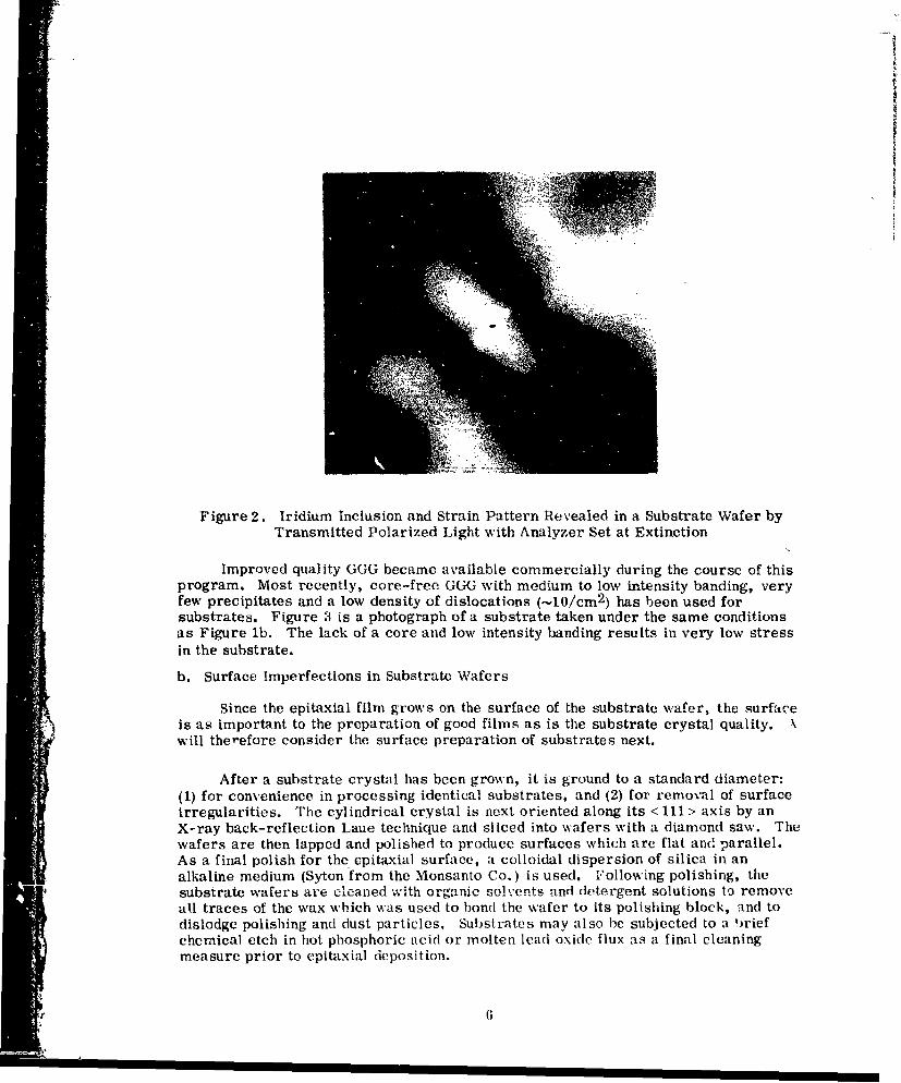
Figure 2. Iridium Inclusion and Strain Pattern Revealed in a Substrate Wafer byTransmitted Polarized Light with Analyzer Set at Extinction
Improved quality GGG became available commercially during the course of thisprogram. Most recently, core-free GGG with medium to low intensity banding, veryfew precipitates and a low density of dislocations (_10/cm 2 ) has been used forsubstrates. Figure 3 is a photograph of a substrate taken under the same conditionsas Figure lb. The lack of a core and low intensity banding results in very low stressin the substrate.
b. Surface Imperfections in Substrate Wafers
Since the epitaxial film grows on the surface of the substrate wafer, the surfaceis as important to the preparation of good films as is the substrate crystal quality. \will therefore consider the surface preparation of substrates next.
After a substrate crystal has been grown, it is ground to a standard diameter:(1) for convenience in processing identical substrates, and (2) for removal of surfaceirregularities. The cylindrical crystal is next oriented along its < 111 > axis by anX-ray back-reflection Laue technique and sliced into wafers with a diamond saw. Thewafers are then lapped and polished to produce surfaces which are flat and parallel.As a final polish for the epitaxial surface, a colloidal dispersion of silica in analkaline medium (Syton from the Monsanto Co.) is used. Following polishing, thesubstrate wafers are cleaned with organic solvents and detergent solutions to removeall traces of the wax which was used to bond the wafer to its polishing block, and todislodge polishing and dust particles, Substrates may also fe subjected to a briefchemical etch in hot phosphoric acid or molten lead oxide flux as a final cleaningmeasure prior to epitaxial deposition.
G(

,II
S!ii
Figure 3. Lack of Stress Patterns Revealed in a Recent (111) Substrate Wafer byTransmitted Polarized Light with Analyzer Set at Extinction
Surface and subsurface scratches produced by mechanical damage during sawingor polishing which have not been completely removed are replicated in the epitaxialfilm, as shown in Figure 4. Such imperfections are barriers to the movement of mag-netic domains in YIG and probably impede the magnetostatic wave. Foreign materialsuch as wax, solvent stains or dust particles on the surface of a substrate act as nucleiso that a film grown over them is not single crystalline, as shown in Figure 5. Amagnetostatic wave is scattered by such imperfections. Surface irregularities such asare produced by imperfect mechanical or chemical polishing produce similar irregulari-ties in an epitaxial film; however, if the irregularity is not abrupt, it does not appearto hinder magnetostatic surface waves in YIG films. In summary, substrates withunremoved surface damage or foreign material produce poor YIG films.
Through the course of this program, continually improving substrate surfacefinishes and the surface cleanliness have been employed as they have been developed onbubble domain programs.
3. EPTIAXIAL FILM GROWTH
YIG films have been grown by chemical vapor deposition (CVD) since the firstcontract in 1966. Another epitaxial growth method which was developed for bubble do-main garnets is isothermal dipping, liquid phase epitaxial (LPE). YIG films have alsobeen grown by this process for this program. A description of the two methods follows,including a discussion of the process variables and limitations of each method.
a. Chemical Vapor Deposition
The CVD process is carried out in a T-shaped reaction chamber, 4 ft wide and4 ft high, made of 3 in. diameter fused silica tubing, as shown in Figure 6. Anhydrous
7

Figure 4. YIG Film Grown on GGG Substrate Which Contained Mechanical Damage
/-!
Figure 5. YIG Film Grown Over Poorly Cleaned Substrate
8
.,

i- SUBSTRATE WAFERSHe + 0 2 INLET EXHAUST
SDEPOSTION QUARTZ "T"
DEPOSIIAE REACTION CHAMBER
_ REACTION ZONE HEATER
"U -QUARTZ INSERT SHIELD
INDIVIDUAL SOURCE Y C3M ATERIAL HEATERS F 2
He + HCI .1 HCI
INLETS
Figure 6. Schematic of T-Shaped Reaction Chamber for CVD YIG Film Growth
iron (11) chloride (FeCo 2 ) and yttrium chloride (YCo 3 ) are contained in platinumcrucibles which are independently heated to control the individual vapor pressures.The vapors mix as they are swept up the vertical portion of the reactor by an inert
carrier gas. Oxygen gas, introduced into one horizontal arm of the reactor, reactswith the chloride vapors where they meet to deposit metal oxides downstream on the
surface of a substrate at 1100 to 1200 0 C. Typical gas flow and material transport
rates are listed in Table I.
Table I. Typical Conditions for the Chemical Vapor Depositionof an Epitaxial YIG Film
Substrate Temperature 11500 C Oxygen Flow Rate 58 m1/m
Vertical Helium Flow Rate 13. 70 f/m YCR 3 Transport Rate 1.23 g/hr
Horizontal helium Flow Rate 4.73 9/m FeC2 2 Transport Rate 11.6 g/hr
11Ce Flow Rate 260 mi/m Garnet Deposition Rate 3.82 um/hr
A characteristic of the CVD process, called the shifting reaction zone (SRZ)behavior (Ref 7), provides a basis for process control. The SRZ is an extension of thethermodynamic reactivity principles which control the chemical reactions. Thus, YIGis not the only product formed in the reactor during a deposition run. Depending onthe gas flow conditions and the concentrations of chlorides, 0 and ItCP, the possibleproducts include yttrium oxide (Y2 .0), yttrium orthoferrite (YFeO 3 ), yttrium irongarnet (Y 3 Fe 5 0 1 2 ) and iron oxides (F'c20 3 and Fe 3 0 4 ), or mixtures of these compounds.
9

In any given run as many as four of these are deposited in or near the seed area.These products appear in a very orderly manner, however, and their order of appear-ance is consistent with the chemical reactivity of YC? 3 and FeC12 . Thus, becauseYC1 3 is considerably more reactive than FeC! 2 , Y2 0 3 is formed first in the reactor,followed by YFeO3 , YIG and finally Fe 2 03. The total reaction zone embracing theseproducts can be shifted from run-to-run, and the individual reaction zones, e.g., theYIG zone, can be shifted or expanded at the expense of the other zones. However, thesequence of deposits Is always the same. Additional details and discussion are in Ref 7.
Anhydrous YCe 3 is obtained from the Lunex Co. of Pleasant Valley, Iowa. It ispurified by sublimation in a molybdenum sublimation train at about 1040 0 C. Theanhydrous FeCf 2 is prepared by direct reaction of iron wire with HC2 gas. Storageof the anhydrous chemicals is in evacuated containers, while transfer of chemicalsinto crucibles is performed in a dry box.
In a deposition run, the anhydrous metal halides are loaded into crucibles,weighed, and positioned in separate thermal zones of the reaction vessel. Thevaporized halides mix as they rise up the vertical portion of the T-reaction chamber.At the crux of the T, the halides begin reacting with oxygen to produce metal oxideswhich deposit from the gas stream. Since several products are produced by thereacting chemicals, the growth parameters must be adjusted to maximize the proba-bility of depositing YIG, and minimize the probability of depositing other products inthe substrate zone. Using the SRZ concept to adjust chemical ratios and concentra-tions, the YTG deposition zone may be extended to cover 3. 5 inches,
Once the proper conditions have been achieved and stabilized, the seet, crystalsare pulled into the deposition zone which is located a few inches downstream from thecrux of the T. At the conclusion of a deposition period, the seed cryst I~ - ýre with-drawn from the deposition zone. The source chemicals are cooled ano weighed todetermine use rates.
The color of YIG in thin-film form is dark green so that its presence on asubstrate is readily evident. Good films are uniformly smooth (uncrazed) and specu-larly reflecting. Full circle X-ray diffraction and back-reflection Laue diagrams showthe magnetic garnet films to be single crystals which are oriented parallel to the substrates.
Among the process variables for controlling YIG deposition by CV) are the gasflow controls which influence the chemical transport rates and the deposition rate.The source chemical purity also determines the evaporation rate and hence the deposi-tion rate. (Since anhydrous chemicals are involved, any premature reaction withmoisture or oxygen reduces the evaporation rate, so that considerable care must beexercised in handling and storing these materials). Individual furnace temperaturescontrol the chemical transport rates and the deposition rate at the substrate. Thus,the process controls for CVD consist of adjusting several gas flows and furnacetemperatures as well as maintaining chemical purity.
The major limitations on the CVD growth process are of two types, growth rateand film imperfections. Good quality YIG films can be grown by CVD at from 3 toG6/m/hr, while higher deposition rates may yield facetted rather than flat films oreven polycrystalline deposits. As a result of this rate limitation, deposition of a10 .tm YIG film requires from 1. 7 to 3.3 hr. A more serious (but related) limitationis caused by imperfections in CVD YIG films which interfere with the propagation of amagnetostatic surface wave. These may be introduced, as indicated earlier, from
10

imperfections in the substrate material and substrate surface. (CVD growth seems toreproduce substrate surface imperfections more rigorously than LPE growth). Inaddition, the CVD process can introduce imperfections in the form of microscopicparticulate matter which falls on the growing film during the course of the deposition.An example is shown in Figure 7. This particulate matter is probably a reactionproduct which had deposited on the wall of the silica T upstream of the substrate andthen broke away. With care in process control of the deposition, the number of micro-scopic particles impinging on a substrate can be quite small, but the probability oftheir occurrence increases with the duration of the run. Thus, during 2- to 3-hrdepositions, the number of defects introduced into a YIG film may be so great that anarea needed for device work (0. 5 cm x 1. 0cm), which is free of defects, cannot befound. Thus, at this time, the major restriction on the use of CVD films for magneto-static surface waves is the number of imperfections.
Another less-understood limitation on the use of CVD YIG is the broader line-width that is observed. CVD YIG films on GGG substrates and on flux-grown YIGsubstrates have had linewidths greater than that of flux-grown YIG.
A final limitation is more on the use of GGG as a substrate than on the CVDgrowth of YIG films. This has to do with lattice constant mismatch wherein GGG hasa lattice constant about 0.006 A greater than that of YIG. Thus, CVD YIG films arein tension, and as the film thickness increases, so does the tension. Thick YIG filmscraze. This problem may be overcome by using a substrate with a slightly smallerlattice constant such as has been prepared by substituting some dysprosium forgadolinium in GGG. Unfortunately, at this time, the crystal quality of mixed garnetshas not been as good as that of GGG. Thus, the preparation of uncrazed 10 to 15,u mYIG films by CVD on GGG is marginal.
Figure 7. Microsccpic Particle on CVD YIG Film

b. Liquid Phase Epitaxy
The epitaxial film growth method which has become standard for bubble domaingarnets is isothermal dipping LPE (Ref 8). This process is based on the observationthat melts having the appropriate compop.t, n of flux and garnet can be supercooledover a large temperature range and remain -n the supercooled state, permitting thegrowth of epitaxial films at constant temperature. A schematic of the equipment used,as shown in Figure 8, consists of a heated crucible containing YIG dissolved in a flux,and a means for dipping a rotating substrate wafer into this melt. Thus, in growingan LPE film, the temperature of the melt is lowered from some holding temperatureabove saturation to below the saturation temperature. (The greater the sapersatura-tion, the more rapid the growth rate.) The substrate wafer is lowered into thefurnace and permitted to equilibrate above the melt to prevent thermal shock. Thenthe substrate is rotated and lowered into the melt for a predetermined period. Uponwithdrawal from the furnace, both surfaces are coated with YIG films. Typicalgrowth conditions are presented in Table I1.
The starting chemicals are dried reagent grade Fe 2 0 3 , B2 0 3 , and PbO fromthe J. T. Baker Co. of Phillipsburgh, NJ., and 99.9 Y2 0 3 from Michigan ChemicalCorp. of Chicago, Ill. The chemicals are weighed, ball milled and melted into a50 mg platinum crucible. Next the melt is heated at 1150oC for several hours toequilibrate the solution. The melt is then cooled to 9000C and a substrate isimmersed. If no YIG film forms, the temperature is reduced and the processrepeated until a film does grow. The saturation temperature is thus bracketed by thetemperatures at which a film did and did not form.
S PULL ROD A
MELT THERMOCOUPLE PULRD" CAP
-- RADIATION SHIELDS
ALUMINA TUBE _-SUBSTRATE WAFER
K _______-CONTROL THERMOCOUPLEHEATING ELEMENT PT CRUCIBLE
MELT
REFRACTORY
Figure 8. Schematic of Dipping Apparatus for LPE YIG Film Growth
12
--ih
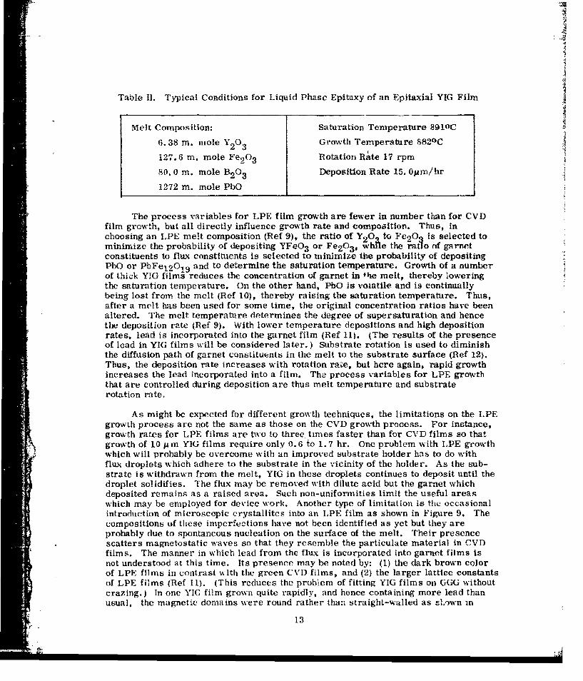
Table 11. Typical Conditions for Liquid Phase Epitaxy of an Epitaxial YIG Film
Melt Composition: Saturation Temperature 891CO
6.38 m. mole Y2 0 3 Growth Temperature 8820 C
127.6 m. mole Fe 2 0 3 Rotation Rate 17 rpm
80. 0 m. mole B 2 0 3 Deposition Rate 15. 0gm/hr
1272 m. mole PbO
The process variables for LPE film growth are fewer in number than for CVDfilm growth, but all directly influence growth rate and composition. Thus, inchoosing an LPE melt composition (Ref 9), the ratio of Y20 to Fe 2 03 is selected tominimize the probability of depositing YFeO3 or Fe 2 03, whfle the ratio of garnetconstituents to flux constituents is selected to minimize the probability of depositingPbO or PbFe 1 2 0O 9 and to determine the saturation temperature. Growth of a numberof thick YFG films reduces the concentration of garnet in the melt, thereby loweringthe saturation temperature. On the other hand, PbO is voiatile and is continuallybeing lost from the melt (Ref 10), thereby raising the saturation temperature. Thus,after a melt has been used for some time, the original concentration ratios have beenaltered. The melt temperature determines the degree of supersaturation and hencethe deposition rate (Ref 9). With lower temperature depositions and high depositionrates, lead is incorporated into the garnet film (Ref 11). (The results of the presenceof lead in YIG films will be considered later.) Substrate rotation is used to diminishthe diffusion path of garnet constituents in the melt to the substrate surface (Ref 12).Thus, the deposition rate increases with rotation rate, but here again, rapid growthincreases the lead incorporated into a film. The process variables for LPE growththat are controlled during deposition are thus melt temperature and substraterotation rate,
As might be expected for different growth techniques, the limitations on the LPEgrowth process are not the same as those on the CVD growth process. For instance,growth rates for LPE films are two to three. times faster than for CVD films so thatgrowth of 10 1m YIG films require only 0.6 to 1.7 hr. One problem with LPE growthwhich will probably be overcome with an improved substrate holder has to do withflux droplets which adhere to the substrate in the vicinity of the holder. As the sub-strate is withdrawn from the melt, YIG in these droplets continues to deposit until thedroplet solidifies. The flux may be removed with dilute acid but the garnet whichdeposited remains as a raised area. Such non-uniformities limit the useful areaswhich may be employed for device work. Another type of limitation is the occasionalintroduction of microscopic erystallites into an LPE film as shown in Figure 9. Thecompositions of these imperfections have not been identified as yet but they areprobably due to spontaneous nucleation on the surface of the melt. Their presencescatters magnetostatic waves so that they resemble the particulate material in CVDfilms. The manner in which lead from the flux is incorporated into garnet films isnot understood at this time. Its presence may be noted by: (1) the dark brown colorof LPE films in contrast with the green CVD films, and (2) the larger lattice constantsof LPE films (Ref 11). (This reduces the problem of fitting YIG films on UGG withoutcrazing.) In one YIG film grown quite rapidly, and hence containing more lead thanusual, the magnetic domains were round rather than straight-walled as sh.wn in
13

Figure 9. Microscopic Particles on LPE YIG Film
Figure 10, and the ferromagnetic resonance linewidth was too great to be measu~red(e.g., over 50 Oe). If lead enters the film as Pb'2, replacing V~3, some chargecompesation must take place to produce electroneutrality. One speculation is that anFe-'- becomes and Fe-4 but this has not been confirmed. It thus seems desirable tokeep the flux ion content of YIG films to a minimum. In summary, the limitations onLPE film growth are not nearly so severe as on CVD film growth; LPE has provided amuch better yield of thick, ancrazed YIG film areas of sufficient size for magnetostaticsurface wave device work.
4. EPITAXIAL FILM CHARACTERIZATION
Although a variety of characterization techniques nave been used on epitaxialYIG films in the past, with the advent of bubble 4ivnnin devices, a number of newtechniques have been developed and made routine. A brief description of the pertinentmethods follows.
Once a film has been grown, it is desirable to determine how uniform the layeris. This is routinely lone by rcflecting iyonochr,, ia'ec light from the wafer and photo-graphing the resulting interference fringe patter-n. 1by using the sodium D line innormal incidence to the sample, tle srnet~fn pacing corresponds to at filmthickness of 0. 128Mm'. Thus, the uniformity ijf ;i finm may be recorded as shown inFigure 11.
44
-KA

(a) Slowly Grown YIG LPE Film
1 b1 Rapidiy Utru~n X IG I PE~ Filmn
: ~ Figure 10. Magnetic IDomains in LPE YIG F~ilms Showing the Normal Straight Domain
Walls of Slow Growth and Curx'cd l)omain Walls of Rapid Growth
•:;, 15
4'1

Figure 11. Interference Fringe Pattern of a YIG Film Showing ThicknessUniformity and Mesas Caused by Flux Retention
After observing the thickness variation of the film, a measurement of thethickness is made in an area of the film which shows good uniformity. The measure-ment is made using a Beckman DK-1A infrared spectrophotometer. For LPE films,the light beam is reflected from the film, while for CVD films, the light is eitherreflected from the film or transmitted through the substrate and film. In either case,one obtains a trace of an interference pattern which is used to calculate the filmthickness.
Under a polarizing microscope, the magnetic domains of YIG are normallyrevealed as an array of parallel plates, as shown in Figure 10a. When a permanentmagnet is brought near, the domains reorient to conform with the magnetic field. Ifimperfections are present in the YIG film, as in Figures 7 and 9, their presence ismade apparent because they pin the magnetic domains. Dark field and Nomarskiinterference contrast microscopy may be used further to investigate imperfections.By use of transducers on the microscope stage coupled to an x-y recorder, it ispossible to prepare a magnified defect map of the film. As the microscope stage ismanipulated to follow the edge of the wafer, the pen of the recorder draws the outlineof the wafer. Then, focusing on pinning defects or mesas permits them to be drawnon the map. The resulting defect map is about 10 times the wafer siae and is conven-iently used to identify regions of the film to be cut out for device work. In the courseof the magnetostatic surface wave propagation studies, ferromagnetic linewidths aredetermined. Thus, the characterization measurements determine film uniformityand thickness as well as something about the quality of the film.
•If

=IIn addition to the more routine measurements, certain special measurements
are occasionally made. Surface roughness is measured with a SIoain Dektak whichmay be used with scales ranging from 106 A to 103 A full scale. Lattice constantmismatch between a film and substrate are measured locally by rocking curves usinga double crystal X-ray diffractometer (Ref 5) and topographs of the entire wafer areprepared by an asymmetric reflection technique (Ref 5). Film composition may bedetermined by electron microprobe analysis. As indicated, this group of measure-ments are only carried out when a situation merits the effort.
At the time this program began, high quality core-free substrates were notreadily available and the growth of YIG films was by CVD. Thus these films werestrongly influenced by the substrate-induced and growth-induced imperfections. Withthe improvement in substrate quality as represented by Figure 3, and the growth ofYIG films by LPE In the latter stages of the program, the film quality was bettered asrepresented by Figures 10a and 11 due both to the reduction in substrate-induced imper-fections and to the growth technique. Since films were evaluated for utility in devicesas they were prepared, a sizable effort was involved in studying the propagation lossassociated with CVD film surface roughness. The results of this irvestigation as wellas a comparison with flux-grown bulk YIG and data from the literature are treated inthe next section.
J
.- 7
SECTION III
FILM EVALUATION
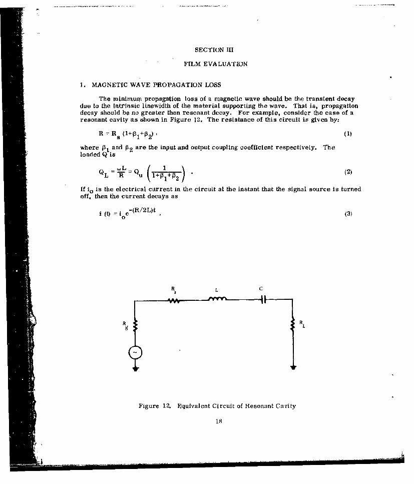
1. MAGNETIC WAVE PROPAGATION LOSS
The minimum propagation loss of a magnetic wave should be the transient decaydue to the Intrinsic linewidth of the material supporting the wave. That is, propagationdecay should be no greater than resonant decay. For example, consider the case of aresonant cavity as shown in Figure 12. The resistance of this circuit is given by:
R = Rsa (1+Pl+P 2 ) , (1)
where P, and P2 are the input and output coupling coefficient respectively. Theloaded Q is
SQ = I'l (2u)+• +•Ii
~L R ki+P1 4P 2 )(,
If io Is the electrical current in the circuit at the instant that the signal source is turnedoff, then the current decays as
(it) 1i e (3)
£R L C
R RLg
Figure 12. Equivalent Circuit of Resonant Cavity

I
where the term due to sinusoidal variation is ignored. By substituting in Eq (2) wehave
-(• / 2QL) ti (t) =I e (4)
0
If the current is measured at two successive times, i(t 1 ) and 1(02), the ratio of currentwould be
i (tl) -(wo/2QL(t-2
1(t 2 )- e (5)
or solving for QL
v f(t2 -t)QL
1(t)
Pn 1(t 2 )
In microwave measurement, signal level ratios, A, are measured in dB, which ar6
ratios of 10 log 0 l i2, hence
Trf (t2-t1) 4.34 Trf(t 2 -t 1 )
log 1 0 (tl) A (7)
4.34
In the case that the propagating wave loss is considered equal to the internal resonanceloss, QL = Qu. That is, no energy is lost to the outside world, but is maintained Inthe resonant structure with its attendant losses. Equation (7) becomes
f 4. 34 Trf (t2-t1)Qu =- (8)
~u~i A
Sincie the intrinsic loss is given by AH,1 4. 34 Tr(t 2-t 1)
Y-- A a(9)
It is now possible to solve this expression for propagation loss aas
Aa = = 4.34nY&Ht 2 - 1
or
a 38.24AH (db/4sec) (10)
19
S. ..... *,.-,-.* .---- . . .•
.- , I i i "J " I i ' I ID

As an example, a I Oe linewidth material would have an e of 38.2 dB/pLsec.Measurements made on epitaxial YIG for the previous cQntract, AFAL-TR-71-275,and reported in the literature (Ref 13) quote a figure of 110 dB/Osec and Brundle andFreedman (Ref 14) quote a figure for flux grown bulk YIG of 300 dB/1 ±sec. Thesefigures represent linewidths of 3 Oe and 8 Oe respectively, considerably above theintrinsic linewidth of YIG.
This discrepancy has been solved on bulk grown YIG by Adam (Ref 15). Hepointed out that mechanical polishing of thE YIG crystal into slabs introduced surfacedamage that interfered with the propagation of the surface magnetic wave. The surfacedamage was confined to a layer several microns thick, referred to as the Bilbe layer.Adams removed the Bilbe layer by chemical polishing techniques and measured thepropagation loss before and after chemical polish. He found that the original 300 dB/pisec was reduced to 27 dB/pxsec after chemical polish. This last figure representsa linewidth of 0. 7 Oe which agrees with the intrinsic linewidth of the material.
The slightly lower (110 dB/p"sec vs 300 dBl/sec) loss in epitaxial YIG is probablydue to the fact that this YIG surface is never mechanically polished, hence no Bilbelayer is present. This figure is still half to one order of magnitude larger than theintrinsic linewidth of epitaxial YIG measured on a previous contract,F33615-69-C-1520, as reported by Besser (Ref 16).
The questions arises - where is the energy going? A similar energy loss inferrimagnet sphere filters has been investigated by Dionne (Ref 17). He assumed thatsurface irregularities gave rise to local demagnetizing fields which either damped orscattered energy into higher order spin waves. This phenomenologlcal theory gaverise to the equation
?6
&H= aHt +A (4TrM)S~5 AH - •intrinsic + A 4M) T-
where A is an experimentally determined constant, 4TMs is the saturation magnetization,d is the diameter of the sphere, and 6 is the depth of the surface irregularity induceddemagnetization.
Other sources of loss in epitaxial YIG films are bulk associated. There aresubstrate induced strain and dislocations, cracks and inclusions grown into the film,and chemical impurity. Fortunately, the effects of strain and dislocations can beminimized by high quality substrates. The rest can be minimized through properattention to growth procedures. Once this is done, it should be possible to examinethe surface contributions to propagation loss in a systematic way.
2. PROPAGATION LOSS MEASUREMENTS ON ROUGH FILMS
A systematic study of YIG films on low defect density GGG has been made. Filmthickness, roughness, and magnetic wave propagation loss have been measured forseven samples ranging in thickness from 1. 9 4m to 15. 5pm. The following observa-tions have been made:
20
-t

1. The film roughness 5 is related to the YIG film thickness d by the relation' : : k3/26-= kd 1/2
where k = 4.75 m-1/2 The roughness is concentric about the substratecenter and appears to follow growth rings of the substrate. The surfaceroughness was measured on a Sloan Technology Corporation Dektak surfaceprofile plotter. The results of this series of measurements are shown inFigure 13.
2. The propagation loss gives rise to the linewidth AH which varies withthickness as
A l k=d-3/2,-9 3,/2
where k' = 56x10 Oe. m 3 2 . This relation holds to about 94m after whichthe linewidth begins to increase with increasing thickness. The propagationloss was measured using a sampling scope and calibrated attenuator. Thereadings were taken at a frequency of 3.39 GHz. A plot of the results isshown in Figure 14. By way of comparison, the data given by Adams wasprocessed to yield loss data for the flux grown bulk YIG plates. It is J.interesting to note that a similar slope is observed, I
3. 'raking observations (1) and (2) together we arrive at the conclusion
AH - kk' where kkl = 252x10 Oe. m.
This result is totally unexpected, implying as it does that linewidth is inverselyproportional to roughness and is independent of thickness (up to 9 Jm).
3. EPITAXIAL GROWTH RINGS AND THEIR EFFECT ON LINEWIDTH
It has been found that expitaxial YIG films do not grow with a uniformly flatsurface, but rather with concentric rings like the rings of a tree or the ripples from astone thrown into a still pond. The roughness of these rings is easily measured witha surface profile probe and the results of a series of measurement indicates that theroughness is directly related to film thickness.
Since the surface magnetostatic wave is a surface phenomena, it would be expectedthat the growth rings would have some effect on the propagation. Such an effect wasobserved. It consisted of reduced attenuation with increased roughness until a criticalfilm thickness was reached, after which the attenuation increased. The improvementin progagation with roughness is a surprising result and an attempt was made to dupli-cate the results by an alternate procedure.
This procedure consisted of taking a thick epitaxial YIG film and polishing thegrowth rings down. The original film was sample No. 2771-1, which was a 13.5 imfilm grown on a low defect density GGG substrate. An 0.3 4m alumina polishing com-pound was used to partially polish down the peaks of the rings. Four data points wereobtained - at the original 2400A unpolished roughness, at two intermediate polishedroughnesses, and at a completely polished surface. The linewidth was measured foreach of these su.Jface conditions and plotted in Figure 15 where a best line fit has beendrawn. As can be seen, the linewidth continues to decrease with increasing surface
21

10.000
5000
0
z
1.00
600-
k d1003
50
=22
I .. L.. I I L .... I... I *jjII
S.1 .5 1.0 6.0 10 60 100S~THICKNESS d (MICRONS)
S~Figure 13. Surface Roughness vs Film Thickness for_ Low Dislocation Density Airtron GGG
S~22
"J'i

50
0
10 -- ~
/"-H K' d- 3
-9
S5.00.5
.001 .005 .01 .05 0.1 0.5 1.0
Figure 14. Linewidth as Calculated from Propagation Loss
22
- -

100
50
0
10 ______
x
.1 11 .1 WLU " I w15 10 50 100
-1 -
I (MICRONS
Figure 15. Linewidth as a Function of Mechanical Polishing on Sample No. 2771-1
24

roughness. After the final polishing, the thickness was remeasured and found tobe 12. 8 nrr_ This is too small a thickness variation from the unpolished film to beconsidered important.
The film was then chemically etched in 113 PO4 at 105 0 C for 5 sec and examinedfor polishing damage under a Nomarski interference contrast microscope. A photo-micrograph is shown in Figure 16. The etch pits due to surface damage are clearlyvisible, and so are the growth rings. A surface profile indicates that the pits are1500A deep and the rings are 100Adeep.
The presence of growth rings on the films implies the presence of these ringsin the substrate material. Surface profile measurements reveal no rings aftermechanical polishing. However, when the substrate is etehed the rings appear.Preferential etching of this sort implies local strain in these rings.
When a core is present in a substrate, it is also strained and may he revealedby etching. The strain in such material is large enough to be observed under crossedpolarizers as shown in Figure 2. A review of the substrates revealed that core strainwas indeed present in Airtron material, but that Linde material was core free.Samples of YIG films grown on cored and core-free substrates were measured bysurface profile and propagation loss. The values are compared with expected valuesfor the cored substrates in Table III.
Figure 16. Nomarski Interference Photomicrograph of Film AfterMechanical Polishing and Chemical Etching
25

Table IJI. Comparison of Properties of YIG Films Grown on Coredand Core Free GGG Substrates
Cored (Airtron) Core Free (Linde)Thickness Roughness Linewidth Roughness Linewldth
3.4k 300A 10.2 Oe <25A 5.4 Qe
10.54 1500A 3.0 Oe 80A 2.50e
The core free substrate films consistently exhibit a lower linewidth, despite having alower surface roughness which suggests that the presence of a core in a substrate hasa greater influence on the quality of a YIG film than the growth rings.
In summary, this study has shown that CVD YIG films grow with a surface rough-ness which reflects the growth bands in the substrate; (1) The line'vidth of such YIGfilms decreases with roughness up to a film thickness of 9 im, beyond which the line-width increases. (The cause of this behavior is not clear at this time.) (2) Polishingdown the roughness of a film thicker than 91 m causes the llnewidth to decrease, and(3) films grown on core free substrates are smoother and have a narrower linewidththan films grown on cored substrates. Thus, core free substrates with a minimum ofgrowth banding are preferable for low linewidth YIG films.
4. PROPAGATION LOSS ON FLUX GROWN YIG
In the previous section, it was concluded that the epitaxial YIG propagation losswas a function of substrate quality and surface condition. For comparison, an initialattempt was made at measuring the properties of flux grown bulk YIG. It was hopedthat measurements on this material would provide a standard for epitaxial YIG. Inaddition, Adam's work would be repeated with the hope of obtaining his 0.7 Oe linewidthfor surface wave propagation.
An 82 gram crystal was obtained from Airtron. It was X-ray oriented and [110]"plates were sliced from it. Infrared and visual inspection disclosed cracks and micro-scopic particles of flux inclusion in the plates. The plates were polished with 0. lrmalumina polishing compound ,Linde B) and a much higher density of included particleswere observed. Since these particles were not originally observed, it was concludedthat the particles constitute alumina grit entrapped in the surface. Figure 17 is amicrophotograph of the surface -- the included grit is clearly visible. Propagation losson these samples measured a minimum of 300 dB/4sec with a linewidth of 8 Oe.
Chemical polishing was then accomplished by dipping a sample in PbO flux at8600 C for 30 sec. Figure 18 shows a photograph of the surface at the same magnifi-cation as Figure 17. The entrapped particles have been removed but the surface isdeeply pitted. A lower power surface photornicrograph, Figure 19 shows a vast net-work of scratches and other damage which the pitting has outlined.
The sample was then etched an additional 60 sec at 8600 for a total of 90 sec.Figure 20 shows that the pits have become wider and begin to overlap. In addition,growth rings, very much resembling the growth rings on epitaxial YIG, have begun toappear. After another minute of flux polishing, Figure 21, the pits have fully over-lapped and become shallower. A lower power photograph, Figure 22, shows when
26
Figure 17. Photomicrograph of Mechanically Polished Flux Grown YIGShowing Included Grit (280X)
Fig.~re 18. Flux Grown YIG Surface after Flux Polishing for 30 Secondsat 8600OC (280X)
27
ia
4llxý b
Figure 19. Detailed View of Surface Damage (55X)
Figure 20. 90 Second Flux Polish at 860 0.C (28X)
28
jr W--- - , -- .--- •-.-;.-

Figure 21. 150 Second Flux Polish at 860 0 C (280X)
Figure 22. Detailed View of Scratch and Grit Included Free Surface (55X)
29

compared to Figure 17, that all the surface damage introduced by the mechanicalpolishing has been removed. All that remain are the shallow pits and growth rings.
Two slabs were cut from this polished sample and the linewidths were measured.Both measured 0.7 Qe. Dimensions and linewidth are compared with Adams in thefollowing.
Thickness Linewidth
This Study 24.5 mils 0.7Oe
Adams 22.2 mils 0.47 Oe
The agreement is quite good and is more in line with the expected linewidth of thismaterial. The 0.7-Oe value compares with a best measured value of 2.5 Oe on a10. 5jm thick epitaxial film.
5. POWER SATURATION IN FLUX GROWN YIG
There is presently little doubt that epitaxial YIG films have a significantly greaterlinewidth than flux grown bulk YIG. Both flux polishing and chemical polishing of YIGslabs yielded the same linewidth when the mechanically damaged layer was removed(2 Nm). This linewidth was 0.70 Oe as compared with 2.6 Ge of the best epitaxial film.
Some confusion in measurement occurred at the beginning since the flux grownmaterial saturated at much lower levels of rf power. Once this was understood,measurements became repeatable. In fact, the saturation becomes a secondary proofof the difference in linewidth between flux and enitaxial material. The critical rf field Iassociated with spin wave instability hcrit is given by
h `(AH ) 11. 5-lA )\l'/2hcrit 2 4TrMs
If two samples are found to differ in saturation by a power level P, where
(- h in dB, then the relative linewidth is
AH 1 P/a0- 10
AH 2
In experiments, the difference between epitaxial YIG saturation and flux YIG saturationis -20 dB, which yields
All 1A-2 4.6A2
This is about the ratio measured by direct linewidth measurements.
30

This result implies that long delay times can only be achieved at the price oflower dynamic range. As a rough estimate, an epitaxial YIG device will have a 74 dBdynamic range as against a bulk YIG device with 54 dB over a 100 MHz bandwidth.
6. CUMULATIVE TABLE OF FILM QUALITY
A cumulative table of CVD films grown for this contract and bulk YIG samplesis given in Table IV. It will be noticed that only two films have been grown with alinewidth under 3. 0 Oe (115 dB/4.sec). While all flux grown bulk YIG slabs havemeasured considerably less than this, bulk YIG cannot be used to achieve nondispersivebehavior. LPE films grown for this pr( gram are not included in the table becausethese films present problems in linewidth evaluation. Since both sides have an LPEfilm, such a film does not have an unambiguous nondispersive region and hence cannotbe measured with the same accuracy as a CVD film. An LPE film could be measuredif the film on the other face were removed, however time did not allow measurementby this technique. Device performance, as discussed in Section V, indicated that LPEfilms performed as well as CVD No. 2771-3(2) which was the best CVD film grown.This is an encouraging situation since LPE films have not had nearly the developmenteffort that CVD and bulk flux materials have had.
7. CONCLUSIONS ON FILM QUALITY
Based on the work during this contract, the surface wave linewidth of epitaxialYIG films is much larger than the intrinsic linewidth of the material, Figure 23 istaken from recent work by Merry and Sethares (Ref 19). The work of both Adams andMerry et. al. is taken on flux grown material with particular attention paid to thequality of surface finish. The top curve is for the epit-axial CVI) film No. 2771-3(3).The epitaxial film has a propagation loss about five times greater than bulk fluxgrown material. There is no inherent reason for this larger loss in epitaxial material,so that with an improved growth process (e. g., liquid phase epitaxy) and improvedsubstrates, it is expected that comparable losses will be achieved - with comparableimprovements in device performance.
it is worthwhile to point out that neither bulk flux grown material •or epitaxialmaterial is yet at the limit of performance. Both loss curves go as fl/3 whereas theintrinsic linewidth goes as fl; hence, even further reduction in loss can be expected.
"31
ft"4 1.
4) ~0
0 0 ) 0 0
CUU rn w C
0L 0 mu m
w0 MO 0 00 0 0 0 0 00 a0Y
S) 00 10
'.0 4)* C) C 0 4 1 0c0 0 0' 0 m> C 0 V- 0
CUU U M --
a) ~ (D a)) (1)r' a) w ) Q ) v Q Q 4) Q) a) 4
Lr t- C11. $4wv 0 t c t l
U)l
rf. 4 g ) 444) Q 0 4))) 4
0004-000 C) 0 0 0 0V44 u- u- u o..u.u
-j 4)4
co m 0
p ":r - q m C. cýt ) IZ 0f 10O1 M~ LO 40 301
7;..~ 1 ~ C4 CO 1 * C; 0 0 0 070c C4 Cý C') U;14 - 4 .-4 -1 q c) o -4 ~ 4 1-4
t-~ t- 'r14~
z ~ ~ ~ ~ ~ ~ - C' z zzmzO
03

300
*~100-
z0
S40
20
10 I I I till ! I1 2 5 10 20 30
FREQUENCY (GHz)
Figure 23. Film Quality
33

SECTION IV
SAMARIUM COBALT MAGNETS
1. PERMANENT MAGNET FIELD STRENGTH AND FIELD UNIFORMITY
The investigation of magnet configurations and dimensions which lead to asuccessful X band delay line and a pulse compression filter are described in thissection. Magnetic field strength measurements are reported for a series ofpermanent magnet arrangements, from the single magnet system which was originallyproposed through various arrangements of two, three, and four magnets. The finalselection was a three magnet system single channel, and a five magnet system dualchannel.
2. PERMANENT MAGNET TASK
The contract defined task was to perform the experimental work necessaryto relate field strength and field uniformity to the aspect ratios of various samariumcobalt magnets. Calculations showed that field strengths of up to 2.5 kilogauss wouldbe needed. A rugged structure which was small and light was required for airborneapplication. The entire project was feasible only after- the recent introduction ofsamarium cobalt permanent magnets which have an energy produce ratio of15K gauss-oersteds (5. 6K for the next highest strength magnet, Alnico V). Since themagnet material was new, it would also be necessary to gain experience in handlingand machining the samarium cobalt.
3. GENERAL MAGNET DESIGN CONSIDERATIONS
For any permanent magnet, the flux density at the gap BG is proportional to:
L• LM H d
L Gand to:
AM Bd
AG
where
L - length of magnetS~M
Ifd = magnetizing force
L G length of gap
AM = cross section area of magnet parallel to pole faces
1Bd - flux density of magnet at operating point
AG area of gap_• 34
- , , -------.---.-----

5r
This shows that for a given air gap the flux density can be controlled by varying thelength of the magnet or the cross section area. As a practical limitation magnetswere not available longer than 0. 93 in.
4. MAGNET FIELD STRENGTH MEASUREMENTS
For uniformity, the axes for the configurations reported here are defined inFigure 24. All field Strength measurements were made with a Hall probe type gauss-meter (RFL Model 1890 serial number 767). Location of the probe relative to themagnet poles were as shown in Figure 25.
a. Proposal Configuration - Single Magnet
The NREG proposal suggested using a single magnet with the YIG located betweenpoles. Several magnets of different dtimensions were measured by Method I ofFigure 25. The highest values obtained, ranged from 0.3 to 0. 88 kilogauss immediately
at the surface. These readings were far below the required 2. 5 kilogauss. Results areshown in Figure 26.
b. Single Magnet-Measured Across Poles Parallel to X-Axis
Values measured using Method 2 of Figure 25 were a little higher than forMethod 1, the largest, thickest magnet giving highest field strengths. Measuredvalues were:
Measurement LocationMagnet Size Edge Center Edge
0.1 x 0.3 x 0.3 in. 0.48K gauss 0.04K 0.6K
0. 1 x 0.6 x 0.6 in. 0.46K 0.05K 0.55K
0. 25 x 0.6 x 0.6 in. 1. 14K 0.05K 1.24K
t -Across Poles Dimension
c. Single Magnet Measured Across Poles Parallel Y-Axis
Measurements using Method 3. Figure 25 were also made and found to yield evenhigher values than Method 2. Data received are as follows:
S~Measurement LocationMagnet Size Edge Caent e r Edge
0.1 x 0.3 x 0.3 in. 0.2K gauss - 1.9K - 0.45K
0.1 x 0.6 x 0.6 0.5K 1.6K 0.3K 1.6K 0.4K
0.25 x 0.6 x 0.6 0.45K 2.5K I.SK 2.25K 0.5K
-Across Poles Dimension
3

U4
z5 z z
Sly -Y
xii riZ
4-4-
11 U' -- 1 01.
NQ
to 36
ZY =

74
(n C)
xx
C--
00
0 0ow
37
SSA WCUT 2.5 in.
-- ' .25 in,
POLE
S~~.•37"5 in.
PROBE LOCATIONS
•0 0L PL
E E
FIELD STRENGTH = .88K GAUSS
DISTANCE FROM
MAGNET SURFACE .3K(IN.)
S0 .37K .21K
.05
.115 .1K
S.08K .1 5S~~.2 5 8 -
- .375 IN. (REF) 09K
Figure 26. Single Magnet Measured Between Poles Parallel Y Axis
.38
d. Dual Magnets - Measured Between Poles Parallel Y-Axis
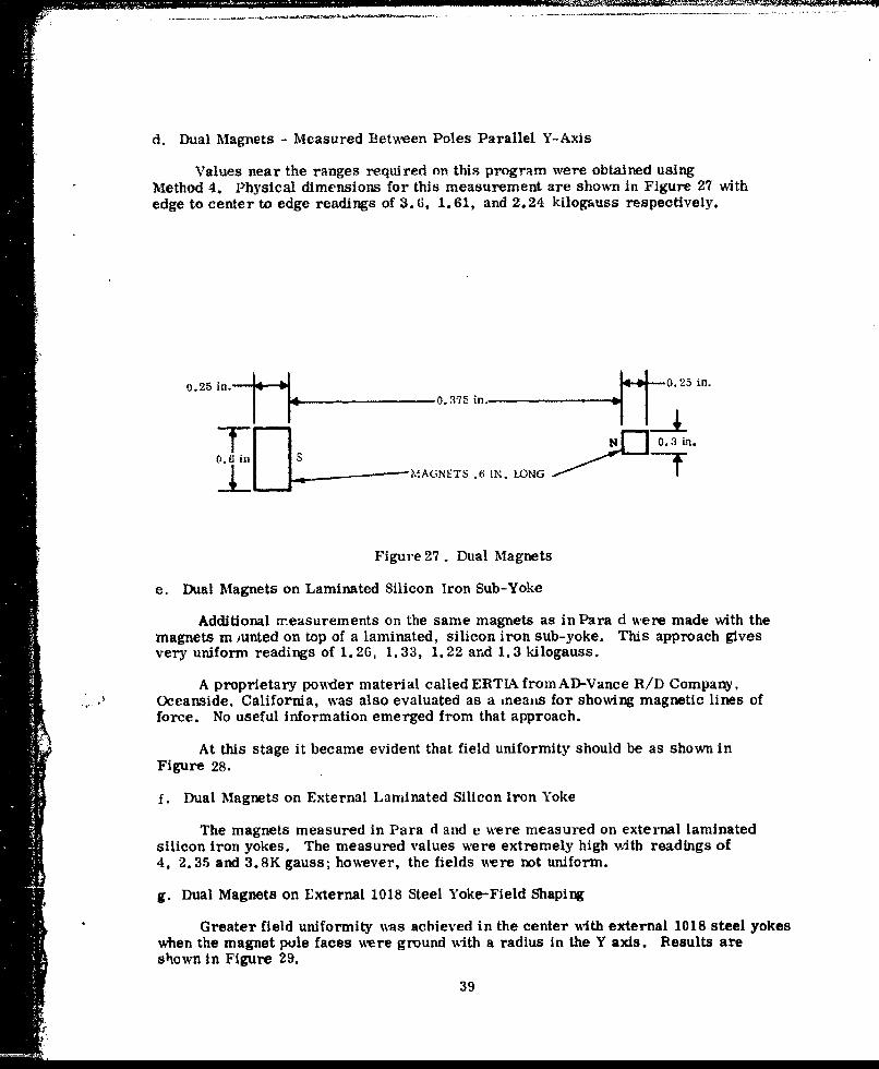
Values near the ranges required on this program were obtained usingMethod 4. Physical dimensions for this measurement are shown in Figure 27 withedge to center to edge readings of 3.6, 1.61, and 2.24 kilogauss respectively.
0.25 in.-I " i--0.25 in.0.375 in.-. 1 I
TN 0.3 in.
MAGNETS .6 IN. LONG
Figure 27. Dual Magnets
e. Dual Magnets on Laminated Silicon Iron Sub-Yoke
Additional measurements on the same magnets as in Para d were made with themagnets mn unted on top of a laminated, silicon iron sub-yoke. This approach givesvery uniform readings of 1.26, 1.33, 1.22 and 1.3 kilogauss.
A proprietary powder material called ERTIA fromAD-Vance R/D Company,Oceanside, California, was also evaluated as a ,neans for showing magnetic lines offorce. No useful information emerged from that approach.
At this stage it became evident that field uniformity should be as shown inFigure 28.
I. Dual Magnets on External Laminated Silicon Iron Yoke
The magnets measured in Para d and e were measured on external laminatedsilicon iron yokes. The measured values were extremely high Nith readings of4, 2.35 and 3.8K gauss; however, the fields %ere not uniform.
g. Dual Magnets on External 1018 Steel Yoke-Field Shaping
Greater field uniformity was achieved in the center with external 1018 steel yokeswhen the magnet pole faces were ground with a radius in the Y axis. Results areshown in Figure 29.
39
_.

0.2 in.
2.5 KIIDGAUSS - AS CLOSEAS POSSIBLE IN VOLUME SHOWN
Figure 28. Area for Required Field Uniformity
h. Triple Magnet on External 1018 Steel Yoke-Field Variation in Y Axis
The addition of a third field defecting magnet,made considerable imprcv'ement inuniformity together with high field strengths. The field had significant variationsin the Y-axis which proved to have great value in the non-dispersive line. Resultsof this measurement are shown in Figures 30 and 31.
i. Cruciform Magnet Configuration
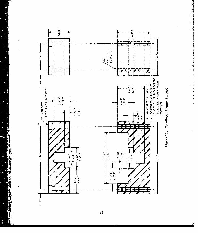
In the central portion of the cruciform magnet configurations in that area to beoccupied by the YIG as defined in Figure 28, the field was found to be uniformwithin about 300 gauss (Figure 32). The cruciform magnet support is shown inFigure 33.
A delay line was built using this configuration, but difficulty was encounteredin changing YIG substrates and positioning the input and output strip line. When thecap containing the fourth magnet was removed it -its possible to produce a functioningdelay. The field for this configuration, which is not quite so uniform, is shownin Figure 34.
J. Triple Magnet Deliverable Device
A functioning delay line was produced using three magnets in the lower portion ofthe cruciform support of Figure 33. The uniformity in the usable area was about350 gauss, but the level dropped about 500 gauss (Figure 34). Positioning of the YIGand the input/output stripline was extremely critical.
40
._ ...-.-. ...---

L a1-
co C4
C9)
CI
C;
41)

- ~~LIIU ~ PROBE "'I. w ant ~ 2aField Strength (K gau.,s)
L L- L-JWith Third
Magnet as
Distance TWO Mlagnects Shown in
"d" (IN_.) Only Position
0 3. 943.930. 2 -•" 0.25" .4.9
.hii 0 1108 2.84 3.55
.. ' .. 2 31 .5 3.6T N NS 0.3', A 2.62 3.62
183/8 3.94 3.93
d"-- o.25"
ALL MAGNETS 0.93 IN. LONG
4.0
K GAUSS
S~3.5-
0 1/16 1/8 3/16 1/4 5/16 3/8
d (IN.)
Figure 30. Effect of Adding Third Magnet
42

S i- PROBEPROBE Distance Field Strength (K gauss)
E D NS d (IN.) h 1/32 In. h=0
"0 3.94 3.94
O 1/16 3.64S-- "1/8 3.33 3.42
3/16 3.23 3. 32
3/8 3.88 3.74
~8STEELT/• / ....,, i1/1 ti
3/32" INSULATION ALL MAGNETS 0.93 IN. LONG
SAME AS FIGURE 30
4.0
K GAUSS
3.5
3.! - . ..J-_I0 1/16 1/5 3/16 1/4 5/16 3/8
D( IN.)
Figure 31. Field Variations in Y-Axis
43

MAGNET 0.375 WIDE X 0.3
d * 4 DEEP X 0.93 IN W)NG
- •• (;AGUSS Cx k)
Distanc e - 5 V 7h'"f 8 d(IN.) 1/16 1f8 1/4 3!8 1/2 5/8 3/4 L'8PROBE
-
MAGNET 0.25 WIPE X 0.3 0 3.3 3.4 3.39 3.39 3.48 3.48 2.98 0.78
DEEP X 0.93 IN. LONG 1:16 2.9 3.07 3.25 3.27 3.26 3.13 2.45 1.04
Sr-- r-r- -; 1 8 2.67 2.86 3.2 3.2 3.15 3.0 2.3. 1.18r- If Fi 3-'16 2. 62 2.8-2 3.16 :1.19 3.12 2.95 2.35 1.26
1 1.4 2.67 2.83 3.1 3.1 3. 08 2.95 2.4 1.233i1 O 5162.9 2.9 3.13 3.1 3.06 3.0 2.7 1.08
h* 333. 47 10.5I.3 II I3 3.2 3.18 3.4 .55______.I_ . L __. : -
SY I,3.5
3. . . . . .. . . . . .
K GAUSS
2.5
2.0 1 1 1 i 10 1/16 1/ 3V/16 1/4 5/16 3/8
d iIN.)Figure 32. Cruciform Magnet Configuration
44
.1
400
IfI
20 I IW (n
04
CD ac~l LnIt ý T ! z '
Im cc0 .1 O 0H77
0 *ft
70 00
I'-5

DISTANCE~ GAUSS (X 1000)
"d" (1 ,) . .28 .46 .64 .8!
0___ ._ o 3.4 3.05 2.83 2.8 3.35
PROBE .1 2.35 2.61 2,72 2.45 2.3
d.2 2,05 2.45 2.63 2.38 1.8
.3 2,5 2. '.5 2.161 1.75
.4 J 8i 2,95, 1 , 2-1 .0 J3. 0
3.5
-- 0. 10Q (h)I
.3.0 0.64
0.28s
0.46
4 2.5
2.0
.- 1 -
0 .1 .2 .3 .4DLSTAN(CE "d"(IN.)
Figure 34. Triple Magnet Deliverable Device
46
t.

An identical structure made about two months after the first gave goodrepeatability.
Magnet curving in the Z axis was attempted, but the one configuration tried%was unsuccessful. It did however, indicate that further refinement will probablyproduce results.
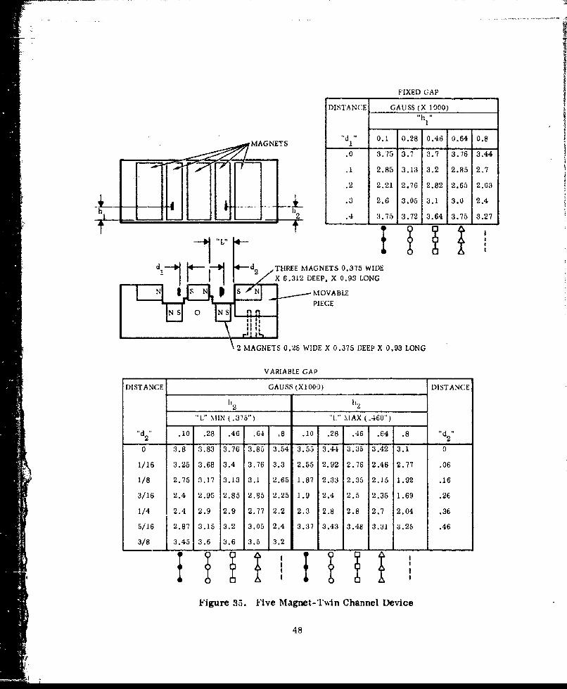
k. Five Magnet-Twin Channel Device
In order to increase the bandwidth, a two channel device wvas constructedwhich shared one of the field magnets thus requiring five, rather than six magnets.One channel was provided with a fixed airgap, and the other with a variable airgapfor field strength/frequency adjustment. The field deflecting magnets were increasedin depth from 0.3 in. on the single channel device, to 0.375 in. This had the effectof increasing the level about 300 gauss, but gave a 50 percent increase in fieldstrength variation. Figure 35 shows the results of both the fixed and variable gaps,and Figure 36 shows details of the five magnet structure.
5. MACHINING AND HANDLING
The magnet supplier recommended cutting and grinding samarium cobaltmagnets with silicon carbide wheels, slow feed, and lots of coolant. Magnets cutand ground in this manner showed a large number of fine to medium cracks.Changing to diamond for cutting and an Aluminum oxide 60K wheel for grinding,both with fine feed and iots of coolant solved the problem. Machining was recom-mended in the uumnagnetized state, but no problem was encountered with magnetizedmagnets. Each ground particle would tend to remain and abrade the grindingmachine long after the magnets had been ground, but ins.fficient magnets wereground to prove this.
Samarium cobalt magnets are very brittle. Magnets 0. 100 in. thick brokeeven when packed with polyurethane foam in plastic boxes 1-3/8 x 1-3/8 x 1 in.The extremely strong magnets would twist a plastic box from the hand whenapproaching another magnet in a box.
Some magnets were supplied with a crack already partly through in the mannerof a manufacturing flaw. These would separate or break if cut near the crack.Magnet strength did not appear lessened by the presence of cracks. Small pieceswould easily chip from sharp edges. Breakage could easily occur with movementoccurring during magnetization. When magnets were improperly bonded to thealuminum magnet structure some magnets were damaged when they broke free aftera time.
6. SUMMARY
Magnet configurations were developed having field strengths of 2.5 kilogaussand above, suitable for both dispersive and non-dispersive X-band delay lines.
The two configurations developed have a low weight potential because theyrequire neither magnetic pole pieces nor yokes, only a minimum supporting structure.
47
FIXED GAP
DISTANCE GAUSS (X 1000)
"dI 0.1 0.28 0.46 0.64 0.8
.0 3.75 3.7 3.7 3.76 3.44
It .1 2.85 3.13 3.2 2.85 2.7I .2 2.21 2.76 2.82 2.65 2.03
4- .3 2.6 3.05 3.1 3.0 2.4h h
L1., 2 .4 3.75 3.72 3.64 3.75 3.27
d- 4---d 2 ,THREE MAGNETS 0.375 WIDEX 6.312 DEEP, X 0.93 LONG
N *SN S N MOVABLE
PIECEN S 0 nS flIiII SI
II II
2 MAGNETS 0.25 WIDE X 0.375 DEEP X 0.93 LONG
VARIABLE GAP
DISTANCE GAUSS (XIO00) DISTANCE
S2 112
"L" MIN (.375") "1." MAX (.460")"d10 .28 .46 .64 .8 .10 .28 .46 .64 .8 "d2"
2 2o - I0 3.8 3.83 3.76 3.85 3.54 3.55 3.44 3.35 3.42 3.1 0
1/16 3.26 3.68 3.4 3.76 3.3 2.55 2.92 2.76 2.46 2.77 .06
1/8 2.75 3.17 3.13 3.1 2.65 1.87 2.33 2.35 2.15 1.92 .16
3/16 2.4 2,95 2.85 2.85 2.25 1.9 2.4 2.5 2.35 1.69 .26
1/4 2.4 2.9 2.9 2.77 2.2 2.3 2.8 2.8 2.7 2.04 .36
5/16 2.87 3.15 3.2 3.05 2.4 3.37 3.43 3.48 3.31 3.25 .46
3/8 3.45 3.6 3.6 3.5 3.2
Li I IFigure 35. Five Magnet-Tuin Channel Device
48
I.

4.0-
3.5
: m /3.0
2.0-
FIXED GAP
1.5 i , .0 .1 .2 .3 .4
DISTANCE "d"
Figure 35. (Cont)4.0
3.5 %0
o3.0 -x
S"2.5 2
Figure0 35 Cot
MINIMUM
VARIABLE GAP
S 1/16 1/8 3/16 1/4 .5/16 3,/8DISTANCE "d2
Figure 35. (Cont)
• 43

4.0
3.b
IMAXIMUMVARIABJLE GAP2 3.0
I. 6 I I I0 .06 .16 .26 .36 .46
DISTANCE d2
Figure 35. (Concluded)
6. SUMMARY (CONT)
Samarium cobalt magnets can be easily machined in the unmiagnetizedcondition using diamond saws or aluminum oxide 60K grinding wheels, with slowfeeds and lots of coolant.
Extreme care must be exercised when handling in order to avoid chippingand breaking. Particular care must be used when magnetizing or when a magnetis near a magnetic surface (or other magnet).
A comparison of highest field strength measured, and field uniformity forthe principle configuration tested Is showni in Table V. Values given were selectedto give the most uniform field for each configuration.
5b

"9 2.425" .
. 1.850"
9 1.475"
S-1.025"0.255"-
d • .,0.700" - 1
0.25400
1-0.400i _.25 -- • 00.425"0-00.042: 7 TYP
0.,255-" 01 /
0.912" ". T 0. 20"0.260" 0.600-
____________ A4 TYP
Sl J_ ... 1Tl-0.475"
20.900"
r/ i 0.500"
" IIMILL SLOT AND COUNTERBORE 20-
FOR 6-32 CAP H-D SCREW 0. 350"ITEM I - 6061-T6 TOLERANCE t. 002 in.
Figure 36. Magnet Structure for Five Magnet Twin Channel Device
51

•II
i 1 .177 , 58•6--,--
M
.396 .186
.385 -6-32lb i,.520 o *J .... ,'-- --
I I
I II• ooR aI 010 R MAX
2.00 1 4 PLACES 9b0
I IIT
I : II
SI I ; II
I SHAPE
" I I OPTIONAL I I
_______ AT ENDS ~LSCLEAR
.588---4 6-32 SCREW .2-
/ FLAT WITHIN
.001
_ -I ITEM 2 6061-T6
-- I - -- TOLERANCES t .002 IN.
ji " I"II .
.4 754
CENTERED
Figure 36. (Cont)
52

FLANGE LEVEL WITH EDGE
• .020 SUBSTRATE
TAP 6 HOLES AND PROVIDE NON-MAGNETIC SCREWS FOR 3
CONNECTORS. CENTRAL CONTACTTO JUST REST ON .020 SUBSTRATE
ITEM 2 (CONT)
Figure 36. (Cont'
53
t.

.32.3 1 0.950
N 'I , . -. 6 1 2
.302 0
K5 225 - 4 .
575 498
ITEM 3ý6-32 PROVIDE NON -MAGNETIC 6061-T6CAP SCREW TO FIT WITH ITEM I TOLERANCES*CLOSE SLIP FIT IN ITEM 1 1 .002 IN.
Figure 36. (Concluded)
54
-I

=i.i
Table V. Comparison of Various Magnet Configurations
Highest Field FieldMagnet Measured Uniformity
Configuration (Kilogauss) (KMlogauss) Comment
Single Magnet 1.9 None No Good
Dual Magnets 3.6 2 Poor Uniformity
Dual Magnets on 1.33 0.11 Field Strength Too LowSiFe 3ubyoke
Dual Magnets on 4 1.65 Poor UniformityExternal SiFe Yoke
Dual Magnets on 3.6 1.66 Poor Uniformity,External 1018 HeavyYoke
As Above + Y 2.56 1.26 Poor Uniformity,axis magnet Heavyshaping
Triple Magnets 3.7 0.15 OK, Heavyon External1018 Yoke
Cruciform 3.2 0.25 OK
*Triple Magnet 2.72 0.34 OK, can probably be(Modified improvedCruciform)
*5 Magnet-Twin 3.17 0.32 OK can probably beChannel Improved
* Final Selection
55

SECTION V
X-BAND DEVICES
1. X-BAND NONDISPERSIVE DELAY LINE
X-band nondispersive performance was measured in a three magnet device fortwo different films. The films were No. 2771-3(2) and No. 2771-3(3) and represen-ted two slices from the same CVD YIG film of 10.5 im thickness. The microwavecircuit consisted of two open circuited transmission lines separated by 0.5 cm on a20 mil alumina substrate. The circuit is shown in Figure 37. The dc resistivity ofthe transmission line was initially 20 Q, but this was reduced to less than UZ afterelectroplating with gold.
The impedance of each port is plotted over the range of 8. 5 to 9.5 GHz in Figure 38.As can be seen, the circuit without the presence of the YIG represents an impedancemismatch of greater than 10:1.
The YIG sample No. 2771-3(2) is then placed into the circuit and shifted aboutuntil a nondistorted delayed pulse is obtained in a pulse delay set up. Once this wasaccomplished the impedance of both ports was plotted as shown In Figure 39.
The mismatch is now less than 3:1 for a frequency of 8.415 MHz, which impliesa mismatch loss of about 1.2 DB per port, or 2.4 DB total.
3/8 in.
.... -38 in.-3/
Figure 37. Microstrip Circuit on 20 Mil Alumina
56
Vt

Figure 38. 30 Mil YIG Feed 4. 5 cm of Air Line
57

Figure 39. 30 Mil Feed with No. 2771-3(2) YIG and 4.5 cm Air Line
58

A transmission and phase plot is shown for this device in Figure 40, Theamplitude plot shows a minimum insertion loss of 25 DB at 8.385 GHz with a -3 DBbandpass from 8. 374 to 8.405, or a bandwidth of 31 MHz. The transmission loss iscalculated from the difference of the insertion loss and the mismatch loss as 22.6 DB.
The delay time is calculated from the phase plot by using the relation
-tdw 2wAfI
Since each vertical sweep represents a AM = T, the same point on every other sweepis 2', and the above equation becomes
2t 1 -1(see
The calculated delay +ime is shown at the top. As expected, the bandpassoccurs in the plateau region of the time dispersion. A total delay of 120 usec with anexcursion of ±6 nsee is obtained. The loss per microsecond is 22.6 DB/120 nsec174 DB/Fsec, which implies a linewidth of 4.55 OG. This agrees with the 4.0 Gemeasured in a uniform electromagnet at X-band which implies a field uniformity toabout 0. 5 Ge for the samarium cobalt structure. The feedthrough level is approxi--nlately down by 35 D13. Attempts to reduce this level by meral partitions were notsuccessful.
In order to determine the delay repeatability due to sample characteristics,the No. 2771-3(2) was replaced with No. 2771-3(3), a different cut sample from thesame YIG deposition, and the parameters were remeasured. Figure 41 shows thatthe YIG is matched to a ratio of 2:1 (0.5 DE reflection loss), which implies a 1.0 DBmismatch loss. Figure 42 shows the bandpass and phase measurements for thisdevice. The delay is calculated as 125 nsec ± 4 nsec over a 3 DB bandwidth of 45 MHz.A rubber grommet was found to actively suppress feedthrough to about 45 DB.
A comparison of the results is shown -n Table VI.
Table VI. Two 10.5 Films at X-Band
I Delay per InsertionSample No. 0.5 cm Loss Bandwidth Linewidth
2771-3(2) 120 t 6 nsec 25 DB 31 MHz 4.55Ge
2771-3(3) 125 ± 4 nsec 20 DB 45 MHz 4.0 0e
59
(03SN) IAVll akNll
U)z0
'a
fl
CU
44U
co-
IIj
C;i
600

Figure 41. No. 2771-3(3) YIG
61

7-~
13.
00
bOD
LIL
0
4 I4Lo
(2)NzLQ3L(32
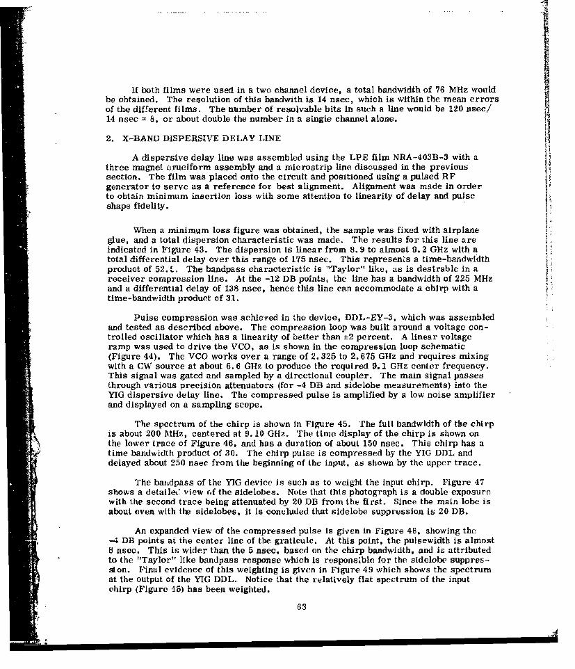
if both films were used in a two channel device, a total bandwidth of 76 MHz wouldbe obtained. The resolution of this bandwith is 14 nsec, which is within the mean errorsof the different films. The number of resolvable bits in such a line would be 120 nsec/14 nsec = 8, or about double the number in a single channel alone.
2. IC-BAND DISPERSIVE DELAY LINE
A dispersive delay line was assembled using the LPE film NRA-403B-3 with athree magnet cruciform assembly and a microstrip line discussed in the previoussection. The film was placed onto the circuit and positioned using a pulsed RFgenerator to serve as a reference for best alignment. Alignment was made in orderto obtain minimum insertion loss with some attention to linearity of delay and pulseshape fidelity.
When a minimum loss figure was obtained, the sample was fixed with airplaneglue, and a total dispersion characteristic was made. The results for this line areindicated in Figure 43. The dispersion Is linear from 8.9 to almost 9.2 GHz with atotal differential delay over this range of 175 nsec. This represents a time-bandwidthproduct of 52. ". The bandpass characteristic is "Taylor" like, as is desirable in areceiver compression line. At the -12 DB points, the line has a bandwidth of 225 MHzand a differential delay of 138 nsec, hence this line can accommodate a chirp with atime-bandwidth product of 31.
Pulse compression was achieved in the device, DDL-EY-3, which was assembledand tested as described above. The compression loop was built around a voltage con-trolled oscillator which has a linearity of better than +2 percent. A linear voltageramp was used to drive the VCO, as is shown in the compression loop schematic(Figure 44). The VCO works over a range of 2. 325 to 2.675 GHz and requires mixingwith a CW source at about 6.6 GHz to produce the required 9. 1 GHz center frequency.This signal was gated and sampled by a directional coupler. The main signal passesthrough various precision attenuators (for -4 DB and sidelobe measurements) into theYIG dispersive delay line. The compressed pulse is amplified by a low noise amplifierand displayed on a sampling scope.
The spectrum of the chirp is shown in Figure 45. The full bandwidth of the chirpis about 200 MHz, centered at 9. 10 GHz. The time display of the chirp is shown onthe lower trace of Figure 46, and has a duration of about 150 nsec. This chirp has atime bandwidth product of 30. The chirp pulse is compressed by the YIG DDL anddelayed about 250 nsec from the beginning of the input, as shown by the upper trace.
The baudpass of the YIG device is such as to weight the input chirp. Figure 47shows a detaileC view of the sidelobes. Note that this photograph is a double exposurewith the second trace being attenuated by 20 DB from the first. Since the main lobe isabout even with the sidelobes, it is concluded that sidelobe suppression Is 20 DB.
An expanded view of the compressed pulse is given in Figure 48, showing the-4 DB points at the center line of the graticule. At this point, the pulsewidth is almost8 nsec. This is wider than the 5 nsec, based on the chirp bandwidth, and is attributedto the "Taylor" like bandpass response which is responsible for the sidelobe suppres-sion. Final evidence of this weighting is given in Figure 49 which shows the spectrumat the output of the YIG DDL. Notice that the relatively flat spectrum of the inputchirp (Figure 45) has been weighted.
63

S50
-0 so225 -LS
200 -40
1 2 7 52 2 v za)• 12 db p ts. /0
150 / 30Sz
- 125 -
100 20
7-5
50 - DISPERSION 10
DISPERSIVE DELAY LINE
25 USING LIQUID PHASE EPI-YIG0o.28[1 THICK (NRA 403B-3)
I I I _.
8.9 9.0 9.1 9.2FREQUENCY (CHz)
Figure 43. Dispersive Delay Line Using LPEYIG 10.28 ým Thick (NRA 403B-3)
64
MENE
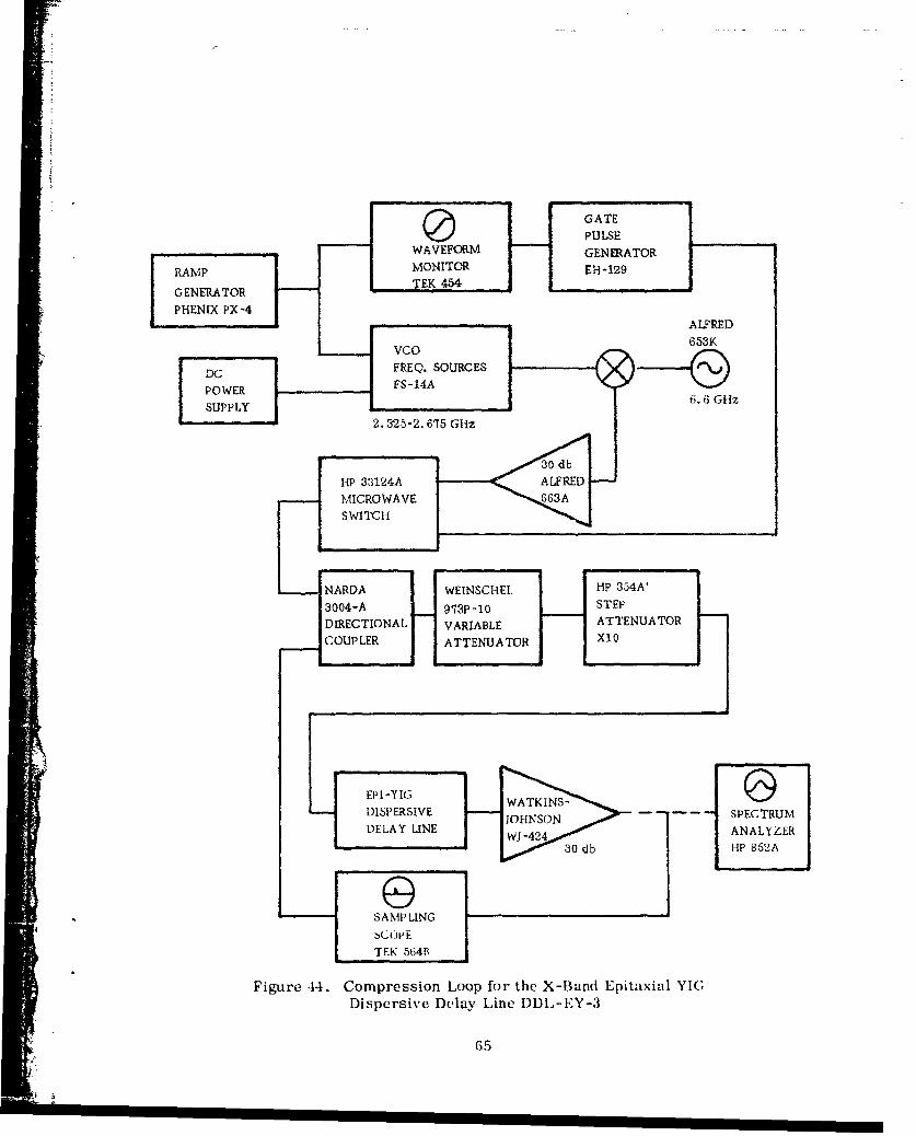
GATEPULSE
.:WAVEFORM GENERATOR
RAMP /MONITOR EH-129
GENERATOR • TEK 45
PHENXPX-4LFRED
653KVCOFREQ. SOURCESFS-14AS~POWER
! 6.6 GHz
SUPPL 2. -325-2. 675 GHz6. z
HtP 33124A ALFRED
EPI-YIG 0M DISPERSIVE SPECTRUM
SWITCHN
DELAY LINE I HANALYP 3ER
3004-A MST0EdbPDELAYP LINEGJ-2 AAYE
3GO dbH 1A _
_. TEK 564B
Figure 44. Compression Loop for the X-Band Epitaxial YIG(
Dispersive Delay Line I)DL-EY-3
65 I I I I I I I
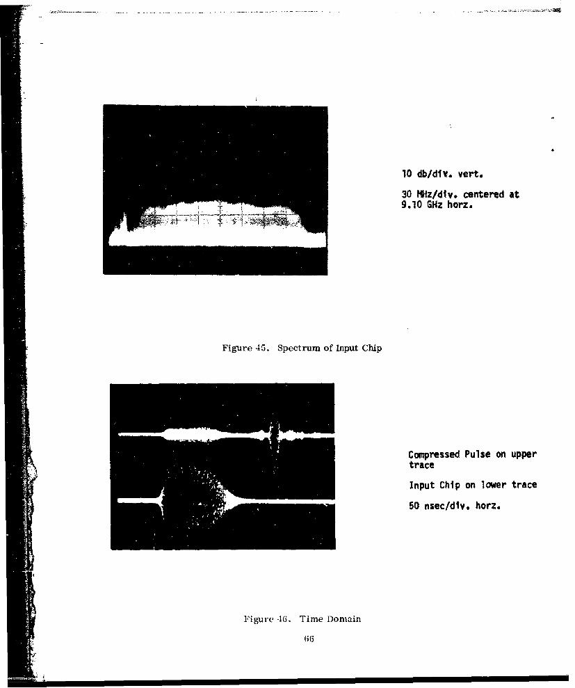
10 db/div. vert.30 t'Iz/div. centered at9.10 GI~z horz.
Figure 45. Spectrum of Input Chip
Compressed Pulse on uppertrace
Input Chip on lower trace
50 nsec/diy. horz.
Figure 416. Time Domain
66
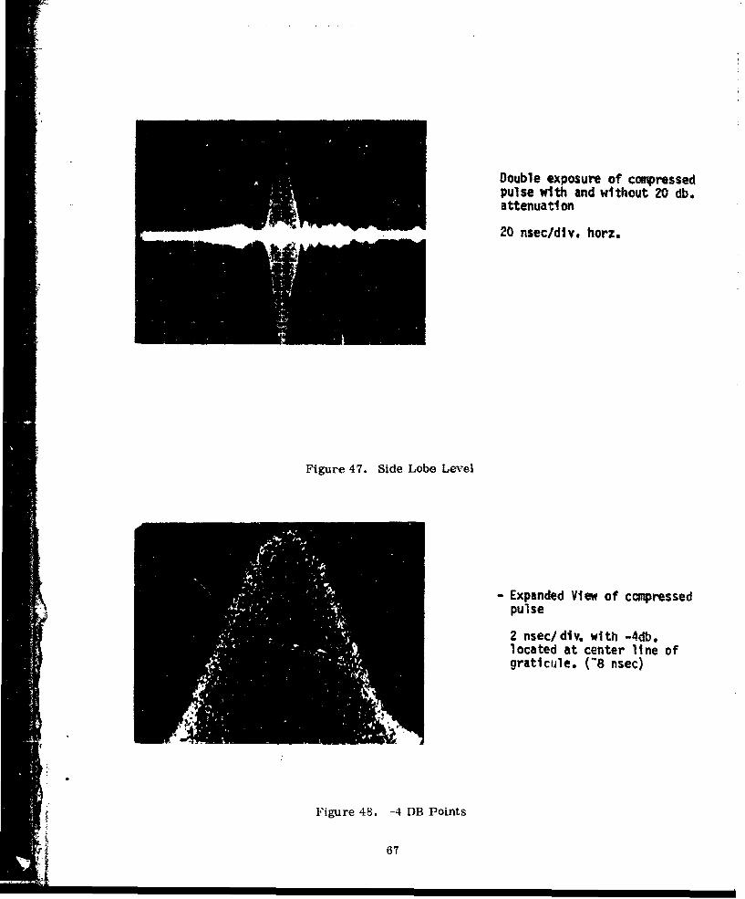
Double exposure of compressedpulse with and without 20 db.attenuation
20 nsec/div. horz.
Figure 47. Side Lobe Level
- Expanded View of ccmpressedpulse
2 nsec/div. with -4db.located at center line ofgraticule. (-8 nsec)
Figure 48. -4 DB Points
67

10 db/dlv. vertl30 Mfz/div, centered at9.10 GHz horz.
Figure 49. Chip Spectrum Weighted by the Dispersive Delay Line
3. SPECIFICATIONS ON DDL-EY-3
The above line was sent to the contractor as satisfying Task 7 of the originalcontract. As such it might be of interest to compare the results obtained with thosegoals originally proposed. This is done in Table VII. Some parameters were missed,namely bandwidth and pulse compression ratio. Others, however, were met orsurpassed - center frequency and insertion loss.
Table VII. Specifications on DDL-EY-3
Goals Device Performance
Center Frequency 9.0 GHz 9.1 GHz
Bandwidth 1.0 GHz 300 MHz Linear Range(Matched to 200 MHz Chirp)
Pulse Compression Ratio 1000:1 52.5 Linear Range(Matched to 30:1 Chirp)
Attenuation Ripple 2 DB -2 DB
Insertion Loss <40 DB 25 DB
Bandpass Response Unspecified "Taylor" Weighted
Dispersive Delay Unspecified 175 nsec(-150 nsec Matched to Chirp)
Delay from Input Unspecified 0.25 4sec: 68
-I

REFERENCES
1. J. E. Mee, G. R. Pulliam, D. M. Heinz, J. M, Owens and P. J. Besser,Appl. Phys. Lett. 18, 60 (1971).
2. C. D. Brandle and A. J. Valentino, J. Cryst. Growth 12, 3 (1972).
3. H. L. Glass, Mat. Res. Bull. 7, 1087 (1972).
4. C. D. Brandle, D. C. Miller and J. W. Nielsen, J. Cryst. Growth 1•, 195 (1972).
5. H. L. Glass, Mat. Res. Bull. _7 385 (1972).
6. R. F. Belt, J. Appl. Phys. 40, 1644 (1969).
7. J. E. Mee, G. R. Pulliam, J. L. Archer and P. J. Besser, IEEE Trans. Mag-5,717 (1969).
8. H. J. Levenstein, S. Licht, R. W. Landorf and S. L. Blank, Appl. Phys. Lett. 19,486 (1971).
9. J. W. Nielsen, "Recent Developments In Crystal Growth from High TemperatureSolutions," presented at the All Soviet Union Conference on Crystallography,September 1972.
10. G. W. Roland, Mat. Res. Bull. 7, 983 (1972).
11. E. A. Giess, B. E. Argyle, D. C. Cronerneyer, E. Klokholm, T. R. McGuire,D. F. O'Kane, T. J. Plaskett and V. Sodagopon, AIP Conf. Proc. 5, 110 (1972).
12. E. A. Giess, J. D. Kuptsis and E. A. D. White, J. Cryst. Growth (to be published).
13. W. L. Bongianni, "Epitaxial YIG Microwave Circuits," AFAL-TR-71-275,September 1971.
14. W. L. Bongianni, J. Appl. Phys. 43, 2541 (1972).
15. L. K. Brundle and N. J. Freedman, Electronics Letters 4, 132 (1968).
16. J. D. Adam, Electronics Letters _, 718 (1970).
17. P. J. Besser, et al, "Epitaxial Growth of Ferrimagnetic Garnets,"Contract No. F33615-69-C-1520.
-4 18. G, F, Dionne, J. Appi. Phys. 43. 1221 (1972).
19. J. B. Merry and J. C. Sethares, "Low Loss Magnetostatic Surface Waves atFrequencies Up to 15 GHz," to be presented at 1973 Intermag Conference in
IWashington, D. C.
4--'I69

UNClASEIFIEDSecurzity Cleaaificatitm
0.~~u~ft? DOCUtAINT CON4TROL DATA - R & D ufft)
(Socttlyý10.Mcojo f MI, boy o obstrmict andJnu4 Iia0xfg nasatlý mostr 6 entered whIen fhoO09. rfi# 1veaJ c.p l aseho
I ORMINIATII4g ACTI~tVY (Corp.1. o&PoofJ Ofe . T ~ rSECURITY CLASSIFICATION
Electronics Group2b Ru
MICROWAVE FILTERS AND DELAY LINES
4 )1 OF2c I"'IV .. Orgs(p fr ~ dadftc. to.dm.)Final Report 8 May 1972 - 29 December 1972
W. 1. Bongianni
D. MRUC Heinz
L. Aeeha 7 -N-73OF
reotd April 1972) Ote reuet fo th1dcm9tms ereerdtI&AF TAL/TEM Wrgh-atero AFA, 7H 4O5433." O'l EPR NM
F36572C16 C72-585/501S I 50iSqNCSLI~rY*~ss
"apDicaibtions aimte Micowv frequoenmntAencies. Tewroverdly; thist rndepoatuwaiodirecutedimportveent wAsri accomplithed byqueproving thes qoumlity ofueptaa be rfe lms, intaon
contract ~ ~ ~ ~ Ai severa devinies wer bil ad vauaed Teswre~. . Anonisprsie ela lie a 8.25 zWrigthPatdelayof 124 Fsece Baniserto
loss ~ ~ ~ ~ ~ ~~Oi of2454ad33anwdh f45M
17 sgiiane of dhiserentialc deayd Thisvevipmen compresed aAiercirp byrc aeie facmtoreeofr 3mall aigdtweightesld sthte adacntegae s icide lob ies total -20 dinlrcesn
3.pliatwon ata delroayvie haviungis a h wod oprsik doeela of 50 i nseor and 80incteThescifcessy of tuhes devices inperatsn of Xiz hand (perating fre2.nc rHTepefresentsaconierable incrledsgnh sae of othei wartv orte frpaairst tnimlecthic sigalerdesigntuer, hasnthopotulzngity tonerfyporuc signalrocussingalt radrsgnals furequncites weith doevies wyhichacompractibeerldevwiths were andl Mand soalduated signal sources.
los of 20. 7 UNanCabanwithFIE5D~z2. Adisprsiv deay lne oeraing t 9.1 Gl wth a300 az inea dispersiontu of

"UNCLASSIFIEDS4eicuity C.AtifiCatein
14 LINK A Lt,,- LINK C.FY wouoi
ROLE fT $ROL t w ROLE
Epitaxial YIG
Magnetostatic Wave
Dispersive Delay Line
Nondispersive Delay Line
Magnetic Wave Devices
Magmtoostatlc Mode in a Dielectric LayeredStructure
it
UNCIASSIFIEDSecurity Clossafication