UNCLASSIFIED AD 291 66i · PDF fileUNCLASSIFIED AD 291 766i ADf ... 4.3 Synthesis of ZI(0)...
58
UNCLASSIFIED AD 291 7 66i ADf ARMED SERVICES TECHNICAL INFORMATION AGENCY ARINGTON HALL STATION ARLINGTON 12, VIRGINIA UNCLASSIFIED
Transcript of UNCLASSIFIED AD 291 66i · PDF fileUNCLASSIFIED AD 291 766i ADf ... 4.3 Synthesis of ZI(0)...
UNCLASSIFIED
AD 291 766iADf
ARMED SERVICES TECHNICAL INFORMATION AGENCYARINGTON HALL STATIONARLINGTON 12, VIRGINIA
UNCLASSIFIED

NOTICE: When government or other drawings, speci-fications or other data are used for any purposeother than in connection with a definitely relatedgovernment procurement operation, the U. S.Government thereby incurs no responsibility, nor anyobligation whatsoever; and the fact that the Govern-ment may have formulated, furnished, or in any waysupplied the said drawings, specifications, or otherdata is not to be regarded by implication or other-wise as in any manner licensing the holder or anyother person or corporation, or conveying any rightsor permission to manufacture, use or sell anypatented invention that may in any way be relatedthereto.

ANTENNA LABORATORY
Thnia bped No. 64
ANTENNA IMPEDANCE MATCHINGCq BY MEANS OF ACTIVE NETWORKS
291 7S61 by
Contract AP331637)-SA6Oit) Hitch Elemntw Nv. 62405454
7600-Prolect 4026, Took 402624Aeronautical Systems Dison
Project Eoglw L Turner, ASRNCV.1
NOVEMBER 1962
Sponored bp:AIONAJTCAL SYSTEMS DIVISIO
VAW~N-PATTOSON AIR FORCE BASE, 01410
A S TI IA
DEC 2 71962
TISIA
ELECTRICAL ENGINEERING RESEARCH LABORATORYENGINEERING EXPERIMENT' STATION
UNIVERSITY OF ILLINOISURBANA, ILLINOIS

Antenna Laboratory
Technical Report No. 64
ANTENNA IMPEDANCE MATCHING
BY MEANS Of
ACJ'IYE NETWORKS
by
S. LaxpatiR. Mittra
Contract A133 (657)-8460Hitch Element Kr. 62405454
760D - Project 4028, Task 402624Aeronautical System Division
Project Engineer Z. Turner, ASJWC1-l
November 1962
Aeronautical Systems DivisionWright-Pattearson Air Force Base, Ohio
ELECTRI CAL ENOINEERING 335 AMO LABORATORYENGINEERING UPMENWT STATIONK
UNIVERSITY Or ILLKNOXSURBANA, ILLINOIS
ABSTRACT
The paper introduces several schemes for wideband matching of
impedances using active elements in the matching network. It is shown
that the design procedure is a straightforward one when two active
elements such as negative impedance converters are used. An alternate
scheme using one active element is also discussed and it is shown that
a RC matching circuit using Kinariwalas' synthesis technique usually
obtains a rather complicated and sometimes impractical type of network.
However, a simple . matching network may be designed using one active
element if certain approximation of the load impedance function is
made, Illustrative designs using one and two active elements are
described in thr paper.
The noire performance of an active matching circuit which has an
infinite bandwidth in Atu Ideal sense is compared with a simple active
pudding network. It is found that there is little relative advantage
of one over the other. It is shown, however, that there is a definito
advantage of the former circuit over the latter one if one compares
their power performance,
Experimental verification of the theoretical designs are included
in the puper.

CONT NTS
Page
Abstract ±
1. Introduction 1
2. 0eneral Scheme of Matching 2
3. Design of the System 4
3.1 Determination of Antsnna Equivalent Network 43.2 Design of Matching Network [-2X(S)] 4
3.2.1 Design by Means of Two Active Elements 43.2.2 Jesign by Means of One Active Element 5
4. Examples 7
4.1 Antenna Equivalent Impedance Z(5) 74.2 Synthesis of Z1(S) using RC elements 8
4.2.1 General Procedure 8
4.2.2 Computations for the Z (S) 101
4.3 Synthesis of ZI(0) using LC elements 154.4 Simplification of Network by means of Approximation 19
5. Noise and Power Considerations 24
5.1 General Considirations 24
5.2 Noise Considerations
5.2.1 Noise Figure Of Network of Figure 16(a) 245.2.2 Noise Figure of Network of Figure 16(b) 26
5.3 Power Considerations 27
6. Uxperlmental Work 30
7. Conclusiuns 39
References 40

ILLUSTRATIONS
Figure Page
1 Antenna Equivalent Impedance 1
2 Scheme for Matching Arbitrary Impedance 2
3 Equivalent Load on the Generator 2
4 Scheme for N..tching Simple Load Impedances 3
B Matching Network Using Two Active Elements 4
6 Cascade Matching Network Using One Active Element 5
7 A Simple Equivalent Impedance of an Antenna 7
8 Matching Network for the Impedance of Figure (7) 8
9 Block Diagram for Cascade Synthesis of Y (a) 9
10 a and B Ladders of the Four Terminal Network 131 15
11 Two "erminal Network with Input Impedance YL12 Complete RC Matching Network for the Z1 () 1s
13 Complete LC Matching Network for the Z (8) ls
14 A Second Antenna Equivalont Impedance 19
15 A Simplified LC Match Ang Netwrk 20
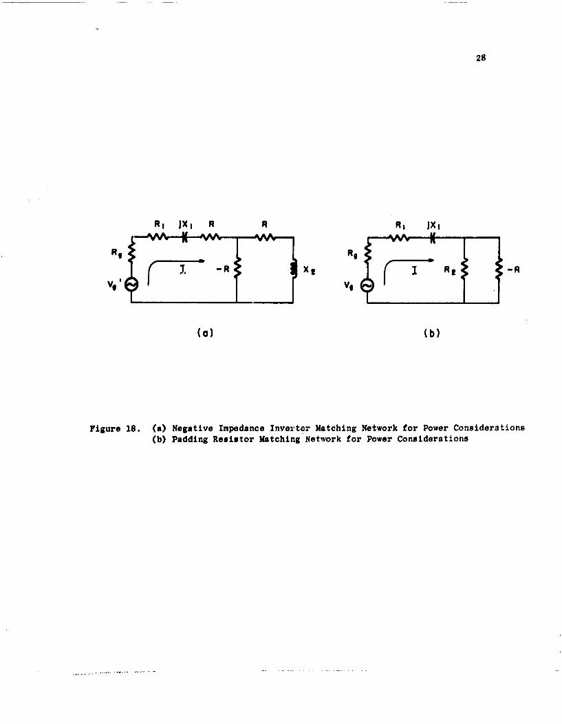
1s (a) Negative Impedanca Inverter Matching Network(b) Network Matching Impedance by Means of Padding Resistor 23
17(a) Negative Impedance Inverter Network with all Noise Sources 24
17(b) Network Matching Impedance by Means of Podding ResistorqWith all Noise Sources 26
1$ (a) Negative Impodance Invorter Matching Network for PowerConsiderations(b) Padding Resistor Matching Network for Power Considerations 28
19 Negative Impedance Converter Number 1 31
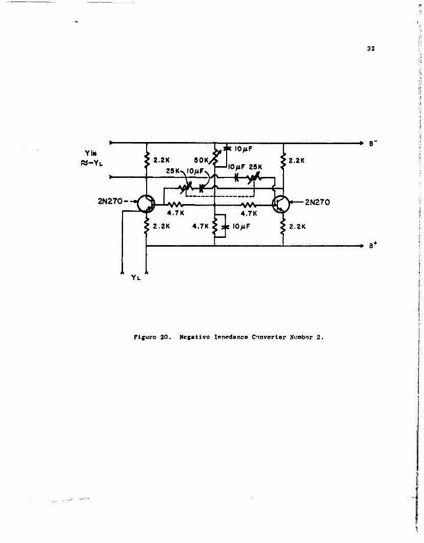
20 Negative Impedance Converter Number 2 32
21 Negative Impedance Converter Number 3 33
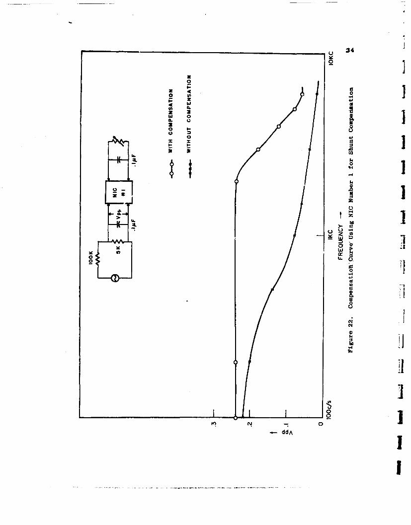
22 Compensation Curve Using NIC Number 1 for Shunt Compens.tion 34
23 Compensation Curve Using NIC Number 2 for Series Compensation 35
24 Compensation Curve Using NIC Nur& er 3 for Series Compensation 36
25 Compensation Curve for Oeries Resonence Equivalent Impedance 37
26 Compensation Using Two NIC a 38

1. INTRODUC'ION
The input impedance of an antenna is a complicated function of
frequency and as such cannot be put into an analytic form for all frequencies.
However it can be approximately represented ovor a frequency band by a lumped
element loasless network terminated by a resistance Rr as shown in Figure 1. V
The complexity of this two terminal pair losle5s network is dependent on
the degree of approximation of the impednace curve of the antenna in the
desired frequency range.
Z(S) R+IX , 1 2 Rr
NETWORK,,
Figure 1. Antenna Equivalent Impedance.
When the antenna is electrically short, it has a high Q and is a highly
frequency sensitive device. It can be approximated by a large capacitive
reactance in series with a resistance. In order to use these antennas
efficiently over a band of frequencies, various impedance matching techniques
are employed.
This problem of matching of antennas using passive networks, based on
different matching criteria has been treated extensively by various authors1' 2.
Fano 3 in his paper, has discussed limitations on passive network, matching
of arbitrary impedance. Not much work has been done on the matching pro-
blem using active networks.
This report is a study of the possibility of using active networks for
antenna impedance matching.

2
2. OZNBRAL SCHIME OF MATCHINO
The proposed scheme (Figure 2) Is for a general type of matching circuit for
an antenna load which admits an equivalent representation of the type shown
in Figure 1. It can be easily shown that the impedance Zin' input impedance of
the cnmposite network is a pure resistive, and is equal to Rr,
ACTIVE
NETWORK
II
I/c___ N TWORK I NETWORK
Z(S) sR+j X
Figure 2. Scheme for Matching Arbitrary Impedance
We can thus represent the equivalent generator load as shown in Figure 3.
If the generator impedance R is taken as Rr, it is obviuus that the power
transferred to the load R is a maximum and constant.
R 9:Re
uZing ra
Figure 3. Equivalent lead on the Generatov

Since the network in Ftgura 2 has input Impedance R r' and has all itu
elements lossless except the load resistance Rrx the power transfer to this
load is constant and maximum. This Rr in cse of the antenna equivalent
network is the radiation resistance of an antenna.
When R , tho even part of Z(J) (real part of Z(W)) is constant a simple
matching scheme of the type shown in Figure 4 may be used.
ACTIVE
NETWORK
-x NETWORK Rr
leo
Z(S) S Rr+X(S)
Figure 4. Schome for Matchifng Simple Load Impedances
The bandwidth of the system in Figure 2 would be dependent on the band-
width of the active network and also the frequency band over which the
equivalent representation of the antenna impedance is employed. Thum the
bandwidth of the system would be lower than either one.

3. DION OF THE SYSTEM
3.1 Dtermination of Antenna Equivalent Network
The process of determining the lumped element equivalent network re-
presentation is largely an empirical one. If the impedance variation as
a function of frequency is available, to obtain ratioaal function of the
form of quotient of polynomials is a standard process It will be assumed
here that either the quotient of polynomials representation of antenna
impedance or a complete equivalent network is available and our discussion
will only pertain to the design of a matching network.
3.2 Design of Matching Network C-2X(S)]
If the form of the Impedance function Z(S) is known, finding X(S) is
just a matter of working out the algebra. Then the major problem is to
synthesize an active network which will produce an impedance of -2X(S)
at its input trrminals. Various schemes for doing thi& are described below.
3.2.1 Design by Means of Two Active Elements
We shall first describe a simple way of synthesizing an impedance function
C-2X(g)]. Figure 5 shows this method wherein it is required to use two active
elements. One of these is a negative Impedance converter while the other is
a negative resistance. This negative resistance can Very well be a negative
impedance converter terminated by resistance Rr, The two four terminal lo.isless
networks vrown are identical and they are the some as the four terminal loesless
networks employed in equivalent antenna impedance representation In Figure 1.
SXl1 X22 Rr
I LCI o j [ NETWORK
N I
-2X(S) 1 2X(S)
X1l X22 -RrLC
NETWORK
Figure 5. Matching Network Using Two Active Elements

3.2.2 Design by Means of One Active Element
We shall now study the possibility of designing this network by means of
a single active element.
4Kinariwala has shown that "any driving point immittance function can bo
realized by a transformerless RC structure tn which is embedded only one
active element. The only restriction on the Immittance function is that it
is a ratio of two polynomials with real coefficients." A more practical method
has been suggested by him in the same paper but with added restrictions on
the immittance function. This results in a cascade network as shown in
Figure 6. The restriction on the immitta'ce is that in addition to its having
real coefficients, the function is positive on some interval of a-axis (J89+jw),
Z2 "N
Z(S) Z1 Z22 R1RC - NETWORK
I l o NETWORK j 2 _jt
Figuro 6. Cascade Matching' Neowork Using One Active Element
Carlin and Youla have shown in their paper that "any arbitrary real,
rational driving point immittance function whose zeros and poles are completely
unrestriczed as to multiplicity and location in the complex S-plane, may be
realized as a lumped network consisting of reciprocal lossless elements and
at most one positive and one negative resistor."6
Rohrer has used a method of synthesis similar to that used by Kinariwala,
but for LC networks. This neework structure In the same as in Figure 6, where
the two terminal network and four terminal network are LC networks.
The function -2X(S) that we wish tn design has indeed tts representation
as a quotient of polynomials of real coefficients. Thus by means of any of
the above techniques one is able to design this impodance uRing either only
RC or LC elements and one active element. The active element is either a NIC
or a single negative resistor. Use of transformers in synthesis of a fouLr
terminal network can be avoided by use of a method suggested by Fialkow
and Gerst7 In case of AC networks, where as the same can be achieved in
case of LC networks by performing an impedance level change similar to
loop impedance level change on a Darlington network.
Examples of synthesis using Kinariwala's synthesis method for RC
networks and synthesis using LC elements are worked out in the next section
of this report.
It should be noted that these methods of synthesis do not always lead
to a practically realizable networx. This is largely due to the arbitrariness
in the choice of certain factors.
7
4. EXAMPLES
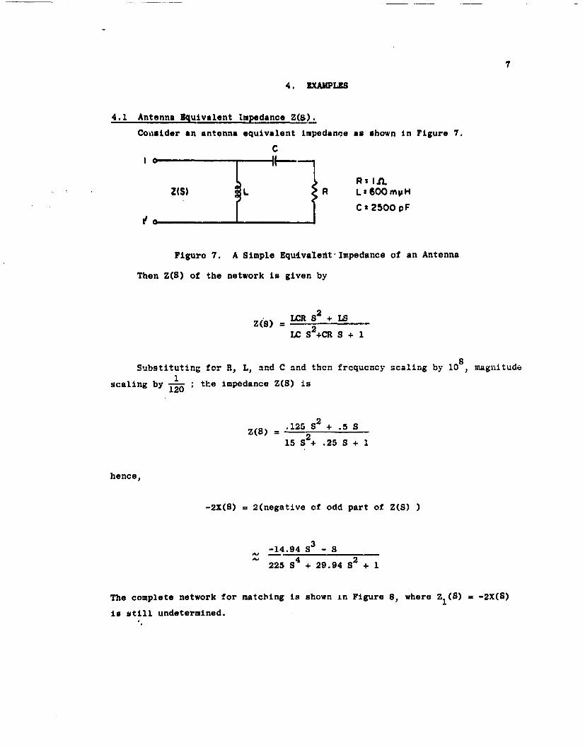
4.1 Antenna Equivalent Impedance Z(S).
Coitsider an antenna equivalent impedance as shown in Figure 7.
C
R I
ZIS) L R L:600myH
C 2 2500 pF
Figure 7. A Simple Equivalent' Impedance of an Antenna
Then Z(S) of the network is given by
Z(S) = LCR S2 + IS
WC S 2+CR S + 1
Substituting for R, L, and C and thcn frcqucncy scaling by 10 8 magnitude1
scaling by -. ; the impedance Z(S) is
.125 82 + .5 S
15 S + .25 S + 1
hence,
-2X(S) = 2(negative of odd part of Z(S) )
-14.94 S3 - S
225 S4 + 29.94 S2 + 1
The complete network for matching is shown in Figure 8, where Z1 () = -2X(S)
is still undetermined.

ACTIVE NETWORK
Figure 8. Matching Network'Sor-the Impedance of Figure (7)
4.2 Synthesis of ZI(S) using RC elements
4.2.1 General Procedure
We shall summarize here the synthesis iethod suggested by Kinariwala4 using
RC elements. We shall work with admittance function Y (8) rather than impedance1
function Z (S) ar exemplified in his paper, with relevant modifications in the
procedure.Let us write Y (S) 1 N
et1 Zl() = D
Selecting B P2P4 where B has only negative real roots, we can write
N - _
~P41lS D - D -5- Q 1 Q3()
2 4
where N =P1 P3 D =Q -Q;3 and P., P3 Q; Q all have negative real roots.
Rearranging Equation (1) we have
P3 P4
Y1(S) = P 1 2 2 (2)
Ql P

9 k
Also for cascade structure of Figure 9 we can virite
z LY22 L
CoprnYqatos()ad () we obtain, Y (
P P
-YI 2
NY,(S) Y1 122 Y 2 L L RC
NETWORKl/€ NETWORK
Figure 9. Block Diagram'for"Cnornde Synthesis of Y (S)
Comparing Equations (2) and (3); we obtain,
Y P, Q3
(4)
1 P3 P4
We can rearrange Equation (3) and also Equation (4) to obtain the following
(-Y 12) P 1 , Q111
B ) I Y22" YL = Q1 Q3 P 4(5
Q1 P2

10
Using Xquation (1) in above we have
N DP1 + g2P2Y I(a) a - DQi ..
g 2P 2 = NQ1 - DP1 0 P2R (May) (6)
We now give the procedure to obtain the Y parameters of the four terminal
network and YL; using the above information from Equations(4) and (6)
(a) Choose P1 and Q of degrees equal to the rank of Yl(8) such that p i
a RC admittance.(b) Zvaluate Y1 () at some point on the negative real axis farther away
from the origin thap the root of Q, farthest away from origin.
(c) Make Y (a) w Y 1 " Q- at this point by merely multiplying Y1 1 (5)by au aprropriate coistant.
(d) Determine P 2R and find its roots.
(e) Assign appropriate roots to P2 from steps (c) and (d).
(f) DetermineR. Find 2 n R2 N a NR: D' w DR.
(g) Zxpress D in partial fraction to obtain
(h) All admittances are obtained by noting that-Yl2 = _L12 Ql
4.2." Computations for the Zl(S)
We have from previous computations in Section 4.1;
225 84 + 29.94 S2 P 1
- 14.94 S - S
Let us consider
P1 = K (5+1) (S+3) (S+5) (S4.7)
Q1 = (S+2) (S+4) (S+6) (S+8)
n 1
and equating Y s - to Y (B) at S z -10; we obtain K 61.2375.

11
Note that the above choice of roots of 1,1, Q, and the point 5 w -10
are the ones that effec the resulting networks, It is essential that the
be chosen judiciously.
We now obtain P2R a NQ1 - DP,, which gives after considerable algebra
work,
P2 R a 225(B + .0666)(0 + .53)(J + 2.481)(8 + 4.467)(8 '+6.522)
2(S + 10)(S - .00023 8 + .0671)
select
P2 u 225(S + 2.481)(S + 4.467)(S + 6.522)(S + 10)
R - (S .0666)(S + .53)(S - .00023 S + .0671)
We now obtain from above,
Q1 P2
and then put into its partial fraction expansion which is given by
DO Q3 P4 1 (.34085 8 306.49 S 350U.13 5 1313.62 Sj
Q1 P Q1 P 225 5+ 2 + 4 5++ S+ 8
L 3.151 S 736.58 4120 S 223.554 8H 225 + 2.481 + + 4.487 + 5+ 6.52 + 10
Now we identify
1.237F (S + )(S + 3)(S + 5)( S + 7) (7)11l (S + 2)(8 + 4)(S + 6)(S + 8)
12
(s + .06e6)(S + .53)(B 2 .00023 8 + .0671)12 (B + 2)(S + 4)(B + 0)(B 8)
1 .341 306.5 8 3500 + 1313.6 SY22 = 22i . 2 F + 4 + 8 + 8
and
1 f 3.181 5 736.5 5 4120 S 223.55 SYL " 225 + 2.48 + 8 + 4.467 + 8 + 6522 + +10
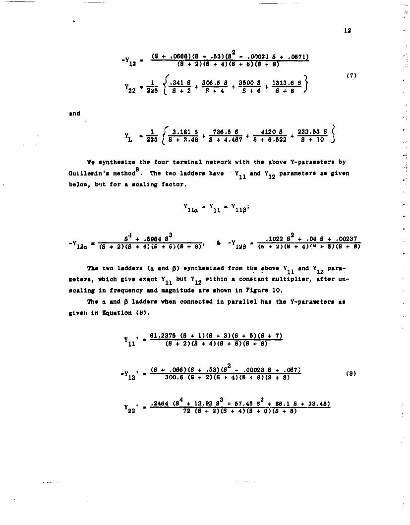
We synthesize the four terminal network with the above Y-parameters by
Guillemin's method . The two ladders have , Y and Y12 parameters as given
below, blt for a scaling factor.
Y lla M Yl ii Yl ip ',
a 4 + .5964 8 3 .1022 S2 + .04 S + .00237"Y 12a (S + 2)(8 + 4)(S + 6)(S + 8)' & "12& -( + 2)(6 + 4)"' + 6)(S + 8)
The two ladders ( and P) synthesized from the above Y and Y12 par&-
meters, which give exact Y but Y12 within a constant multiplier, after un-
scaling in frequency and magnitude are shown in Figure 10.
The a and P ladders when connected in parallel has the Y-parameters asgiven in Equation (8).
, 61.2375 (S + 1)(S + 3)(8 + 5)(S + 7)11 (S + 2)(S + 4)(S + 6)(S + 8)
, (S + .066)(8 + .53)(S 2 - .00023 S + .067) (8)12 300.6 (S + 2)(S + 4)(S 4 6)(S + 8)
Y, .2464 (S4 + 13.93 53 4. 57.45 S2 + 86.1 5 + 33.48)22 72 (S + 2)(S + 4)(S + I)(S + 8)

2.835 K10.64 2.71 .01735 300.6
.0597 .038 091 126
a LADDER29.7 K 238.5 K
F89 1251 17.9 5 K2
316.9~ 492,u -i 859II 2 '9s2
1 LADDER
Figure 10. a and B Ladders of the Four Terminal Network

:L 4
Since we need the Y-purametoru of this four terminal network as in
Equation (6), we use a method of scaling analogoulto that of impedance scaling
Darlington network; as shown below.
We have from Equation (5)
y (S) y (Y11 11 Y21,1 - L
(-Y 1 2)2
11 (Y22 YL-,-(- 121
2
(y -
ll (22'"Y
where
Y11' " p Y1 2 k Y12P Y2 2 Y, L k
Using the ebove in Equations (7) and (8) we have k 1/300.6; and
(V y 1.675 8 10-8 +.1504 10-4 1.72 10 -4 + .645 10-422 L 0 + 2 5 + 4 0 + 6 8 +
1.56 8 10- + .362 10-4 + 2.025 104 + 10+ 2.48 8 + 4.467 1 + 6.522 10 +U '10
(9)
But we have Y2 2 ' as in Equation (8), hencr we obtain using Equation (9);
1,726 1 10-3 + .37 10- 3 +.220S0o3 + 22 10-3 6 10-7L { + 2 8 + 4 8+ 6 8 +8 5 + 2.48
.362 0 2.025 .11 6 10- 415 + 4.467 0 + 0.522 S 10 /I
15
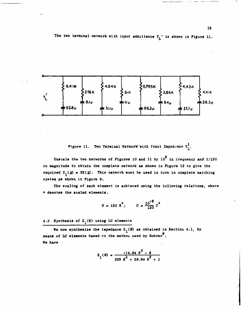
The two terminal network with input admittance Y L' is shown in Figure 11.
0L
6.41M 0 4S4K :15,795K 14.43K
1 427K 91K 2.66K 4.41K
L it 8.1 I .1P 94p 28.3 V62.8 ~ 31.1 p 8 6.3 p3771
0- -
Figure 11. Two Terminal Natworkl with Input Imped.inco Y
Unscale the two networks of Figures 10 and 11 by 108 in frequency and 1/120
in magnitude to obtain the complete network as shown in Figure 12 to give the
required YI(S) = 2X(s). This network must be used in turn in complete matching
system as shown in Figure 8.
The scaling of each element is achieved using the tollowing relations, where
* denotes the scaled elements.
R, 2 10- 8 CR. 120R ; C ="- C
120
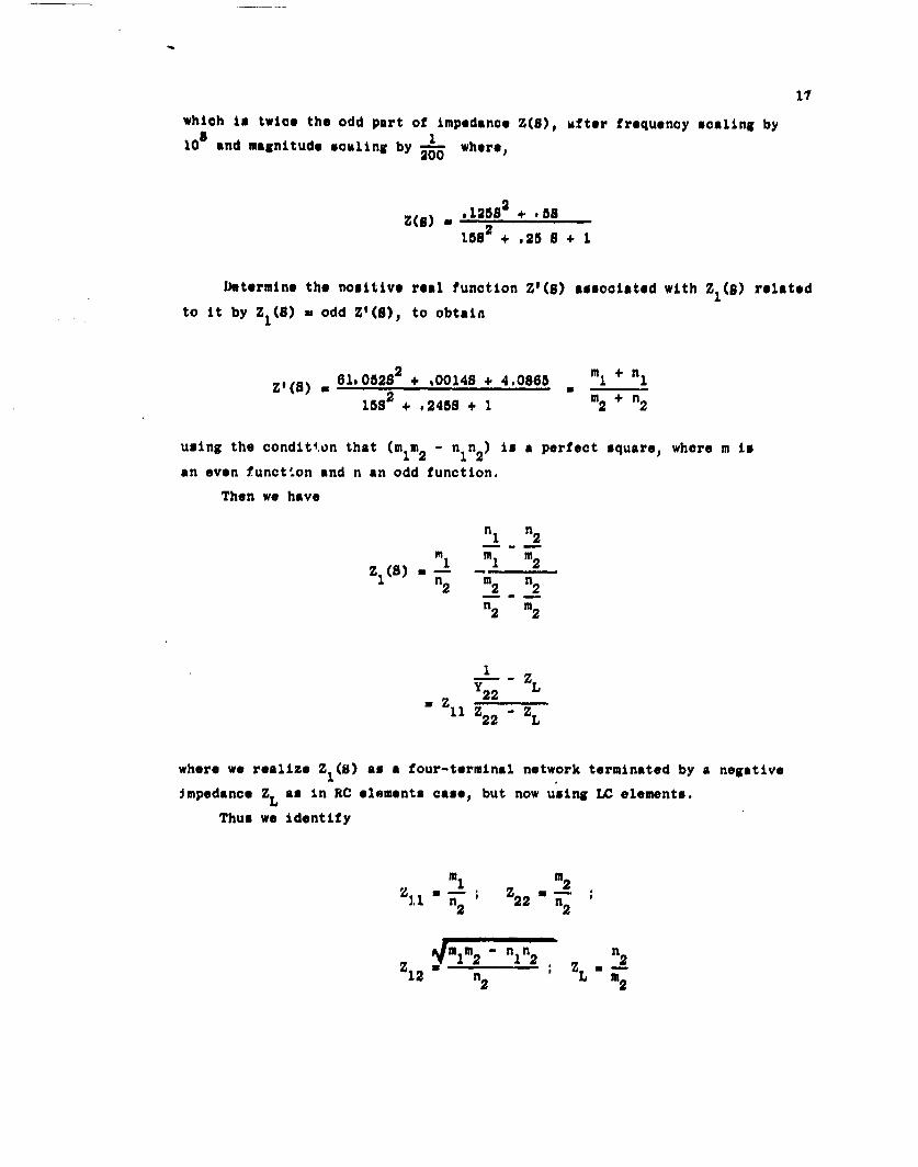
4.3 Synthesis of Z1 (S) using LC elements
We now synthesize the impedance ZI (B) as obtained in Section 4.1, by1 6
means of LC elements based on the methoG used by Rohrer
We have
Z () -14.4 - s225 S4 + 29.94 2 + 1

~~11
2
it A
0 vb
In CLi)ANa
CLIa.k
00
In 06
C-I-
a.6
c"04
IrCI21
NYNJ A
Figue 1, Coplee RC.machig newor fortheZif)
17
which is twice the odd part of impedance Z(S), utter frequency scaling by8 1
10 and magnitude scaling by -L where,
202
Z(S) - o125852 + .58
1582 + .25 + I
Determine the nositive real function Z'(8) assooiated with Z1(a) related
to it by Z1(8) a odd Z'(8), to obtain
ZI(S) x 61.05282 + ,00148 + 4.0865 m + n1
1552 + .2458 + 1 m2 + n2
using the condition that (m1m2 - n n 2) is a perfect square, whore m is
an even functton and n an odd function.
Then we have
n1 n2
Z (S) = 1 2n2 m2 n2n2 m2
1 -. ZL
Y221 Z 22 - L
where we realize Z (8) as a four-terminal network terminated by a negative
impedance ZL as in RC elements case, but now using LC elements.
Thus we identify
"'1 "'2'Zl n' 2 " 22 • n2
m2m - nIn 2 n2
z12 • n2 ; L m2
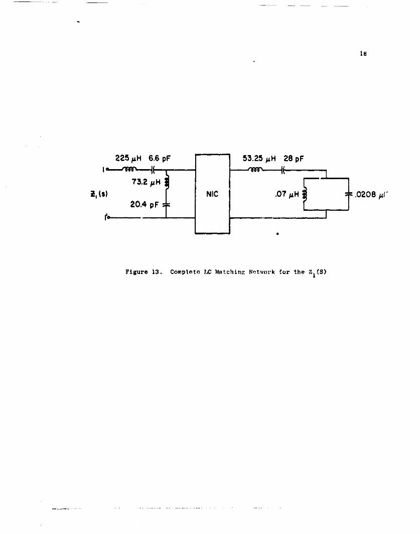
7 3 , 0 I C07)L .0 2 0 8 ,u ( "
Figure 13. Complete LC Mntchingt Nrotwork for the Zi (S)

19
Hence we have the Z Amrameters of the casoado structure as follows:
2]61.0528 + 4.086511 = 245S
22.0215 (14.94S + 1)
12 .245S(10)
15S + 1Z222 .245S
Z u .245S
158 + 1
Unscaled cagcade network realizing ZI(S) is shown in Figure 13, where the
scaled networ', has Z parameters of Equation (10).
This network is In turn used in system of Figure 8 to obtain the complete
system used for matching the impedance Z(S).
4.4 Simplification of Network by means of Approximation
We find in Sections 4.2 and 4.3 that the networks realizing Z 1 vb), which
is twice the negative of odd part of Z(S), are very complicated and sometimes
lead to impractical element values. We find it possible to simplify this
network considerably if we approxinmate the Z1 (s), as shown below in case of a
Z(S) different from that used in Sections 4.1, 4.2, and 4.3.
Consider the antenna equivalent impedance Z(s) as shown in Figure 14.
IMPENOANCE AT 10 Mc/$
C R:I. R :1..
Z(S) L C 250 pF XL: 628 ILL 1OWJH XC: 65 .
Figure 14. A Second.,,Antenna.Equivalent Impedance

20
Hence we have
.0+400S
After frequency scaling of 10 7.and
X= 399*99S 3+ 1600S 11
SS~ + 7-9999S 1
and
Z (s) =-2X (S) - 9.8~ 3200S
1eq S 4 79999S52 + 164
If the matching network for this Z (b) is synthesized on the line of1I
Section 4.3, the network has quite impractical 'element values. But if we
approximate X eqby X1 ' as in Equation (12), we find the network a very
simple one.
3X? 400S + 16008 400S
2 -2(12)eq + +8 + 16 S + 4
and
ZI(S) ~2Xt - 800S1j8 -Xeq- 2 4
Figure 15. A Simplified LC Matching Network

21
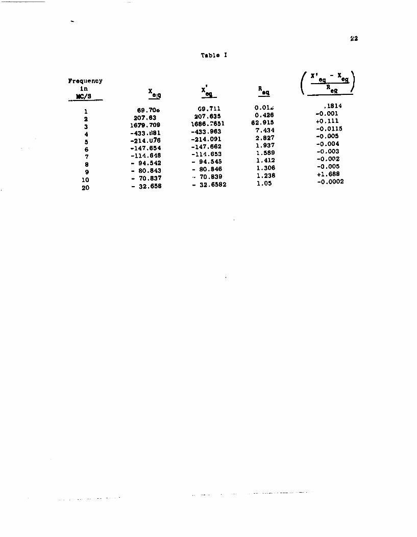
Figure 15 shows the network realizing Z I(b). We now check the error
involved in this approximation and the limitation on the frequency band over
which it is valid. To determine this one muxt consider the ratio of difference
in XeIS to the Req of the known impedance Z(B) since this affects the pror in
the impedance faced by the source. Tabulated in Table I is the factor -eg eg
Reqat different frequencies over thc range of 10 to 1. It is clear that this
ratio is less than 1 over this frequency, and is very small for most of the
frequencies. Thus we can conclude that over the frequency range f.Oriwhich
the , antenna - equivalent impedance of the form shown in Figure 14, the
matching network is exceedingly simple if an approximation of neglecting R is
used.
22
Table I
Frequency ex eq
in X x Req Re0NC/S OR._e
1 69.?70 69.711 0.014; .1814
2 207.63 207.635 0.426 -0.001
3 1679.709 1686.7651 62.915 +0.111
4 -433.td81 -433.963 7.434 -0.0115
5 -214.u76 -214.091 2.827 -0.005
6 -147.654 -147.662 1.937 -0.004
7 -114.648 -114.653 1.589 -0.003
8 - 94.542 - 94.545 1.412 -0.002
9 - 80.843 - 80.846 1.306 -0.005
10 - 70.837 70.839 1.238 +1.688
20 - 32.658 - 32.6582 1.05 -0.0002
23
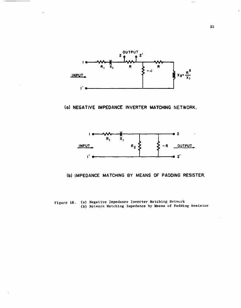
OUTPUT
R, X, R
INPUT, X1
(a) NEGATIVE IMPEDANCE INVERTER MATCHING NETWORK.
R1 :1R -R OUTPUT.
1 I - 0 2
(b) IMPEDANCE MATCHING BY MEANS OF PADDING RESISTER.
Figure 16. (a) Negative Impedance Inverter Matching Network(b) Network Matching Impedance by Means of Padding Resistor
k4
5. NOISE AND POWER CONSIDERATIONS
5.1 General Considerations
In receiving antennas the noise performance of the receiving system Ls a
very important factor, while in a transmitting antenna the efficiency of the
matching system is of primary importance. Thus any matching system should also be
analyzed from point of view in order to ascertain its usefulness. It is often
difficult to make any general statemonts about various systems, and a specific
analysis has to be mada before coming to a definite conclusion.
Let us consider a simple negative impedance inverter type of active matching
network shown in Figure 16. Its performance will be compared with that of the
simple active matching circuit which uses resistance amplification phenouenon.
These two networkp are shown in Figure 16(a) and (b).
5.2 Noise Considerations
5.2.1 Noise Figure of Network of Figure 16(a)
Figure 16(a) shows the negative impedance inverter type of network. R1 and
X1 are the real and imaginary parts of the impedance Z(S) of an electrically
short antenna. (-R) is a negative resistance and X2 an inductance of the value
shown. The noise sources in the system are the thermal noise generators of the
resistors R., and R's. The negative resistance is considered to be a tunnel diode
and its noise current generator ie of magnitude V2el'dAf. It being the d.c.dc dcbias current, e the electron charg-, and Af is the bandwidth. The network of
Figure 16(a) with all its noise sources present is shown in Figure 17(a).
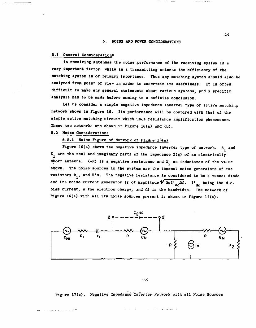
I 2 se
e., R1 eg vR eN eN
Figuire 17(a). Negative Impedance 'Inv-erter'Network with all Noise Sources

25
where
Ni a Thermal noise of resistance R1 " /4k_Ill
•N = Thermal noise of resistance R = 4 (13)
in = noise current of tunnel diode = 2e I'dc
k is Boltzmann's constant.
The noise figure defined on the basis of short circuit current at the
output terminals is
Noise Figure = N.F.
Sum of the square of short circuit noise current at the output terminals
due to all the noise sourcesS'm of the square of short circuit noise current at the output terminals
due to external noise sources alone
We have in this case a negative impedance inverter and associated matching net-
work as the system under consideration for the noise figure analysis. Hence the
noise figure of network of Figure 16(a) is given by
2 e 2 I 12 2 e
N.F. 1 +X+ J X ) - JXI+ J j (R.F : 1 X 12 + j X 2(R- R 1) ' i( + R
2
+ R(R + JX (R JX J 2 2 R)
+ It e2x 2 (R 1 - jX 1 + j - - R alX2
Algebraic simplification using Equation (13) gives
112 R2 + 12 e I(N.F. = 1 + - + - + _R1 - I (14)

26
5.2.2 Noise Figure of Network of Figure 16(b)
Figure 16(b) shows a matching network using a padding resistor formed
by the parallel combination of R2 and (-R). (-R) is a negative resistance
amplifier, and again we consider it to be a tunnel diode.
Shown :n Figure 17(b) is the network of Figure 16(b) with all its noise
sourc3s present.
I RI I T 2R2 -R I
NIlyeN 2
Figure 17(b). Network Matching'Impedance" 6y Means of Padding ResistorWith All Noise Sources
Where we have
eN1 = ,V4kTRl '
aN2 - V(15)
in /2Idc
Analyzing along the lines of Section 5.2.1 for noise figure on the basis
of output short circuit current we obtain, after algebraic simplification
using Equation (15),R2 +X2 12 +12 e
N.F.=1+ R1 + R1 +11 Itdc (16)R 1R 2 R 1 (kT d
From Equation's (14) and (16), one can readily verify that under conditionsX >>R; and X2 Z R (necessary for large bandwidth), these two expressions are
approximately identical. Thus for all practical purposes the noise perfor-

27
mance can be considerud about equal for the two circuits,
5.3 Power Consideration,
To compare Lhe performance of the two systems of Figure 16 for power
requirementmwe determine the power input: to the systems for the same power
dissipated in the antenna equivalent radiation resistance R 1 . The main power
source shown here as in Figure 18 is assumed to hove an internal impedance R ggLet I be the current flowing through the resistance R 1 . A simple analysis
leads to the following results in the two cases under the assumption that the
current delivered to the load is the same in each case.
Case I. Negative impedance inverter matching network of Figure 18(a).
(a) Power output to RIL = Pt = 12R1
(b) Power input by the generator P' ml
- I(R 4 R 1)
(c) Power input by the negative resistor (-R) = PI
= 12 (R + X)
(d) Total power input Pin = Pinl + P'in
= 12j[Rg + R1 + R + X12/RJ (17)
Case I. Padding resistor matching network of Figure 18(b)
(a) Power output to RI = Pout =I2R1
(b) Power input by the generator = P inl
= 12 tRg + R, + Re. "jI 2 XI
(c) Power input by the negative resistor (-R) = Pi n2
(d) Total power input = Pn = P nl + P n2
I2 {Rg 4 R, + Re (T -) -j 12X1 (18)
28
R I jXI R R R I jX1
V-j ____ Xt l R -RV.' V.
(a) (b)
Figure 18. (a) Negative Impedance Invertor Matching Network for Power Considerations(b) Padding Resistor Matching Network for Power Considerations
29RR9
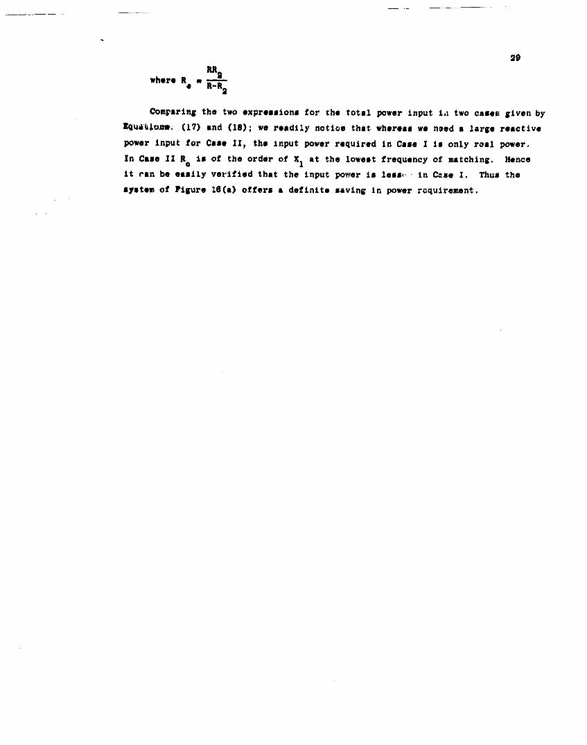
where R R2* R-R2
Comparing the two expressions for the total power input i, two cases given by
Equai'U on (17) and (18); we readily notice that whereas we need a large reactive
power input for Case 11, the input power required in Case I is only roal power,
In Case II Ra is of the order of X1 at the lowest frequency of matching. Hence
it can be easily verified that the input power is less- in Case I. Thus the
system of Figure 16(a) offers a definite saving in power requirement.
3)
6. EXPBRIMRNTAL WORK
The experimental work conducted during this investigation has heon con-
cerned primarily with the matching networks for simple antenna equivalent circuits,
and using negative impedance converters as active elements. The N.I.C.'s ais a
positive fecdback network has, as a rule, a small useful frequency band. Thus
a number of NIC's were built to function in different frequency bands from
1 XC/S to about 10Mc/S. NIC's using tubes were built to function in the
lower frequency range of up to 10 IC/S and successfully tested. Later on,
transistors have been used all throughout in this investigation.
The basic design of these NIC's was brsed on the circuits given by Linvill9
and Bonner 10 in their papers. Figures 19, 20, 21 show three different types of NIC's
using transistors. These NIC's were used in matching simple equivalent impedances
of antenna. The results of these are shown in Figures 22, 23, and 24. In each
figtire is shown the signal across the antenna equivalent resistance with and
without the matching networks compensation.
It is observed that there is a limitation set up at high frequencies, and
this is the limitation in the performance of NIC at these frequencies due to
the appreciable phase shift introduced by the transistors used. The low fre-
quency limitation observed is due to the large ratio of reactive to real
impedance of the antenna equivalent impedance. This ratio is about 25 to 35
at the lowest frequency.
Figures 25, 26 show. the results obtained using twc NIC compensations.

4K IO;0 , K OOK
2N270 2N270INPUT 10~--l014F
tpu F
10K 270XL I1K I0K
LOAD
Figure 19. Negative Impedance Converter Number 1.
32
~-L2.2 K 50K 2.2K
2N270-2N270
4.7K 4.7 K
a+
YL
Figure 20. Negative Impedance Cinverter Numbe~r 2.

2N711 DARLINGTON PAIR
INPUT LOAD
IOK 10K10K
2N711 DARLINGTON PAIR
Figure 21.. Negative Impcdancc Converter Number 3.
0
z J30 0P -4
zw 00 0
.0
8/00
$1 I
0-U.
j*a
C4)4
00
0.4 0
d4.)

z
zz
t 4 J4
8. caUw
00
001-4d..

360
00z0
x
41 wEn a
0.
2
0
00
0
.41
z
U. 4J
290 0
0~ U)0~
.Y.
0 00.-4U
&L. 4J

33
0
I- -
0 0
0 ~x x
0h 0
2. 2
co r0m
z 9f.00
Q U1
C1 ddAi

38
00
0
u0 0
E[
I-00
~ U0zI- I-
0cv.
d4.)
39
7. CONCLUSIONS
(1) Active networks consisting of negative impedance converters or negative
resistances may be successfully used to design wideband matching circuits
for arbitrary load impedances. The design procedure using two active
ele&lents is very straightforward. An R-C matching circuit using one
active element only may be designed using a procedure outlined by Kinariwala,
but the method does not always lead to practical values of circuit components.
L-C circuits using one active element may also be designed to approximately
match a given load. One usually pays the price for reduced number of active
elements in terms of increased complexity of design.
(2) It is difficult to form a general conclusion in regard to tbh comparative
advantages of Pitive matching networks, over a simple active padding network
from the point of view of the noise performances because there are various factors
including the nature of the load ilpedance which determines this behavior. For
a particular case it was found that there is little relative advantage of the
active matching circuit over the padding network, inzofar as the noise
performance is concerned. However, for the same case it was found that from the
point power performance the active circuit had a definite advantage.
(3) Experimental studies demonstrate the feasibility of building the
theoretically designed circuits and show that active matching circuits
perform satisfactorily in the design frequency band limited only by the
bandw'Ath of the active elements and their signal handling capacity.
The general conclusion is that wideband matching may be accomplished
through the use of active elements. However, the complexity of design, the
noise and power performance etc., depend strongly on the nature of the load
impedance to ba matched and the relative bandwidth desired. A study of some
of these aspects has not yet been completed and a continuation of the study
along this line is recommended.

40
REFERENCES
1. H. J. Carlin & R. LaRosa, "Broadband Reflectionless Matching withMinimum Insertion Loss", Proo. of Symposium on Modern Network Synthesis,Polytech. Inst. of Brooklyn, April 1952.
2. N. Yaru, "A Synthesis Method for Broadband Antena Impedance MatchingNetworks", P!..D. Thesms, University of Illinois, 1955.
3. R. M. Fano, "Theoretical Limitations on the Broadband Matching of ArbitraryImpedances," J. Franklin Inst. V 249, p. 57, Jan. 1950 and p. 139 Feb. 1950.
4. B. K. Kinariwala, "Synthesis of Active RC Networks", B.S.T J., V. 38, pp.1269-1316, September 1959.
5. H. J. Carlin & D. C. Youla, 'Network Synthesis with Negative Resistors,"
Proc. IRE, V. 49, No. 5, pp. 907-920, May 1961.
6. R. A. Rohrir, "Active Network Matching of Arbitrery Loads", Electronics Ras.Lab., University of California, Berkeley, Report No. 367, Series 60.June 8, 1961.
7. A. Fialkow & I. Gerst, "The Transfer Function of General Two TerminalPair RC Networks", Quart. Appl. Math., Vol. 10, July 1952.
8. M. E. Van Valkenburg, "Introduction to Modern Network Synthesis", JohnWiley, New York, 1960, Sec. 11.5.
9. J. G. Linvill, "Transistor Negative Impedance Converters", Proc. IRE,V. 41, 7une 1953, pp. 725.
10. A. L. Bonner & J. L. Garriser et. al., "The E 6 Negative ImpedanceRepeater", B.S.T.J., V. 39, n. 6, Nov. 1960, p. 1455.
ANT2NVA LABORATORY
TECHNiCAL REPORTS AND MEMORANDA ISSUED
Contract AF33(616-310
"Synthesis of Aperture Antennas," Technical Report No. 1, C.T.A. Johnk,October, 1954.*
"A Synthesis Uetbrod for Broad-band Antenna Impedance Matching Networks,"Technical Report No. 2, Nichol&@ Yaru, 1 February 1955.* AD 61049.
"The Assymmetrically Excited Spherical Antenna," Technical Report No. 3,Robert C. Hansen, 30 April 1955.*
"fAnalysis of an Airborne Homing System," Technical Report No. 4, Paul H.Mayes, 1 June 1955 (CONFIDENITIAL).
"Coupling of Antenna Elements to a Circular Surface Waveguide," TechnfealReport No. _5, H. S. King and R. H. DuHamel, 30 June 1055.*
"Axially Excited Surface Wave Antennas , Technical Report No. 7, D. E. Royal,10 October 1955.*
"Homing Antennas for the F-66F Aircraft (450-2500 mc)," Technical ReportNo. 8, P. E. Mayes, R. F. Hyneman, and R. C. Backer, 20 February 1957,
(CNIDENTIAL).
"Ground Screen Pattern Fange," Technical Memorandum No. 1, Roger R. Trapp,10 July 1955.*
Contract AF33(610'-3220
"Effective Permeability of Spheroidal Shells," Technical Report No. 9,E. J. Scott and R. H. Duliamel, 16 April 19.56.
"An Analytical Study of Spaced loop AD' Antenna S~'stems," Technical Report,No. 10, D. 0. Berry and J. B. Ireer, 10 May 1956. AD 98615.
"A Tochnique for Controlling thie Radiation from Dielectric Rod Wavcgutdes,"Technical Report No. 11, J7. W. D.mcan anid F. H. DuHazael, 15 July 1956.*
"Direction Characterigtics of a 17-Shapec 5'ot Artenna,' Technical Reportlo. 12, Richard C. Becker, 30 September 1956.**'
"Impedance of Ferrite Loop Ante~inas," Technical Report No. 13, V. H. Rumseytind W. L. Week.,p 15 October 3956. AD 1!9780,
'Closely Spaced Tras,sverse Slots in Pec'angulkr Waveguide," Technical ReportNo 14, Richard F. Pyreman, 20 December 1956.

37Distributed Coupling to Surface Wave Anternas," Technical Report No. 15,Ralph Richard Hodges, Jr., 5 January 1957.
It The Characteristic Impedance of the Fin Antenna of Infinite Length,"I Tech-nicalPReport No. 16, Robert L. Carrel, 15 January 1957.*
"On the Ist.mAtion of Ferrito Loop Antenna Impedance," Technical Report No. 17,Walter L. Weeks, 10 April 1957.* AD 143969.
"A Note Concer"ing a Mechanical Scanning System for a Flush J'ounted LineSource Antenna,' Technical Report No. 16. Walter L. Weeks, 20 April 1957.
"Broadband Logarithmically Periodic Antenna Structures," Technical Report No.19, R.. H. DuHamel and D. E. Isbell, 1 May 1957. AD 140734
"Frequency Independent Antennas," Technical Report K2ro. 20' V. ff. Rumsey,25 October 1957.
"The Equiangular Spiral Antenna," Technical Report No. 21, J. D. Dyson,15 September 10,67. AD' 145019.
"Experimental 1nvestigion of the Conical Spiral Antenna," Technical ReportNo. 22, R. L. Carrel, 25 May 1957.** AD 144021
"Coupling between a Parallel Plate Waveguide, and a Surface Waveguide,"Technical Rp~er1,No. 23, E. J. Scott, 10 August 1957.
"Launching Efficiency of Wires and Slots for a Dielectric Rod Vaveguide,"Tehia epr o 4 J. W. Duncan and R. H. Duffemel, August 1957.
'The Characteristic Impedance of an Infinite Biconical Antenna of ArbitraryCross Section," Technical Report No._25, Robert L. Carrel, August 1957.
"Cavity-Baclred Slot Antennas," Technical Report No. 26, R. J. Tector, 30October 1957.
"Coupled Waveguide Excitation of Traveling 'Vive Slot Antennas," TechnicalRoport No. 27, W, L. Weeks, 1 December 1951,
'Pha'ie Velocities in Rectangular Vaveguide Partially Y'illed with Dielectric,"recncal Rert No. 28 W. L. Weeks, 20 December 1957.
'M3asuring the Capaci±tan'ce per 'Unit Length of 91 conical Structures of Arbi-trary Cross Section," Technical epo2rt No. 29, J. D. Dyson, 10 January 1958.
'Non-Planar Logarithmically Periodic Antenia Structure.," Technical ReportNo. 30, D. P. Isbell, 20 February 1958. AD 156203.
Electromagnetic Fields in Rectangular Slots," Technical Report No. 31, X. J.Kuhn and P. E. Mast, 10 March 1958.
"oThe Efficiency of Excitation of a Surface Wave on a Dielectric Cylinder,"Technical Report No. 32, J. W. Duncan, 25 May 1958.
" A Unidirectionul, Equiangular Spiral Antenna," Technical Report N~o. 33,J. D. Dyson, 10 July 1958. AD 201135
"Dielectric Coated Spheroidal Radiators," Technical "t~port No. 34, W. L.Weeks. 12 September 1958. AD 204547
"A Theoretical Study of the Equiangular Spiral Antenna," Technical ReportNo. 35, P. E. Vast, 12 September 1958. AD 20454R,
Contract AF33(616)-6079
"tUse of Coupled Waveguides In a Traveling Wave Scanning Antenna," TechnicalReport No 36, . H. MacPhis, 30 .April 1959. AD 215558
" On the Solution oL a Class of Wiener-Hopf Integral Equations in Finite andlnfinite Ranges," Technical Report No. 37, Raj hittra, 15 Kay 1959.
"Prolate Spheroidal Wave Functions for Electromagnetic Theory," TechnicalReport No. 38, W. L. Weeks, 5 June 1959.
"Log Periodic Dipole Arrays," Technical Report No. 39, D. Z. Isbell, 1 June1959. AD 220651
"tA Study of the Com-Corrected Toned Mirror by Diffraction Theory," TechnicalReport No. 40,, S. Daegupta and Y. T. Lo, 17 July 1959.
"The Radiationt Pattern of a Dipole on a Finite Dielectric Sheet," TechnicalReport No. 411, K. G. Ealmain, 1 August 1959.
"tThe Finite Range Wiener-Hopf Integral Equation and a Boundary Value Problemin a Waveguido," Technical Report No. 42, Raj Mittra, 1 October 1959.
"1Impedance Properties of Complementary Multiteruival Planar Structures,"iTechnical Report No. 43, 0. A. Deschamps, 11 November 1959.
"On the Synthesis of Strip Sources," Technical Report No._44. Raj Kittra,4 December 1959.
"Numerical Analysis of the Eigenvalie Problem of Waves In Cylindrical Wave-guides," Tee-tia lRepor~t No. 45, C. If. Tang atd Y. T; Lo, 11 March 1960.
"New Circularly Polarized Frequency Independent Antennas with Conical Deanor Omnidirectional Patterns,"I Tech"ical Report No. 46, J. D. Dyson and P. Z.Mayes, 20 June 1960. AD 241321
"Logarithmically Periodic Resonant-V Arrays,' Technical Report No. 47, P. Z.Mayes. and R. L. Carrel; 15 July 1960. AD 240302

'A Study of Chromatic Aberration of a Coma-Corrected Zoned Mirror," Tech-nic.al Report No. 48, Y. 1'. Lo, June 1960.
"Evaluation of Cross-Correlation Methods in the Utilization of Antenna Systems,"Technical Report No. 49, R. H. acPhie, 25 January 1961.
"Syntheel. of Antenr.s Products Patterns Obtained from a Single Array," TechnicalReport No. 50, R. H. MacPhle, 25 January 1961.
"On the Solution of a Class of Dual Integral iquacions," Technical Report No. 51,
F., Mittra, I C-tober 1961. AD 264557
"Analysis and Design of the Log-Periodic Dipole Antenna," Technical Report No.52, Robert L. Carrel, 1 October 1961.* AD 264556
'A Study of the Non-Uniform Convergence of the Inverse of a Doubly-InfiniteMatrix Associated with * Boundary Value Problem in a Waveguide," Technical!t2pr~to , P,, Mttrap I October 1961. AD 264556
Copies available for a threti-week loan period.
Copies no longer availAblo.

I1
AF3I657 )-8460
DIST-1,IBUTION LIST
One copy -ach unless otheruise indicated
Armed Services Tochnical Information Directo-Agency Rallist'cs Research Laboratory
Avtn: TIP-DR Attn: Ballistics Measurement Lab.Arlington Hall Station Aberdeen Proving Ground, MairylandArlington 12, Virginia (10 copies)
National Aeronautics & Space Adm.Aeronuatlcal Systeas Division ALtn: LibrarianAttn: (ASRNCF-3) Langley Field, VirginiaWright-Patterson Air Force BaseOhio (3 copies) Rome Air Development Center
Attn: RCLTLAeronautical Systems Divisicn Griffiss Air Force BaseAttn: ASDSED, V.. Mulligan New YorkWright-Patterrin Air Force BaseOhio Recearch & Development Co.and
Hq. USAF (ARDRD-RE)Aeronautical Syztems Division Washington 25, D. C.
Attn: AFCIN-4BlAWright-Patterson Air Force Base Office of Chief Signal OfficerOhio Engineering & Technical Division
Attn: SIGNET-5Air Force Cambridge Research Washington 25, D. C.
LaboratoryAttn: CRRD Commandinl. Of rLaurence G. tiansco= Field U. S. Army Elelcton:Vs h & D'AckmtyBedford, Massachusetts Attn: Sl'WS-ED
White Sands Missle Rang(. xro anderAir Force Missile Test Center DirectorPatrick Air Force Base Surveillance DepartmentFlorida Evans Area
Attn: Technical Document CenterCommandcr Belman, New JerseyAir Force Missile Development CenterAttn. Technical Library Comnar.derHoll~man Air Force Bas" U S. Naval Air Test CenterNew Mcxico Attn: 'ST-54, Antenna Section
Patuxent sliver, MarylandAir Ferce Ballistic Missile DivisionAttn: Tech .cal Lxbras, Air Force Material Laboratory, Code 932
Unit Post Office New York Naval ShipyardLos Angules, California Brooklyn 1, New York
comi-inding Off icer Boelng Airplnne Compa-yDiamond Ordnance ruse L-tbora:ories Aere Space DivisionAttn: 2-10 Attn: Technafal LibraryWashington 23. D. C. StF Antenni & Radones Uni"
Soattle, Washingt.onDirectorU S. Navy El~ctronlcs Laboratry Boeing A rplane CompanyA:tn. Library Attn: Technical LibrarySan Diego 52. Cjiafornia X/F Antenna Systems Staff Unit
Wich;:A, Kansas
Ad.i..-Rus" I Co=paay200 Sixth Strec: ihance Vought Airczaft Inc.Attn. Library (Antenna Sect:on) siaU: BU AER RepresentativeC.mbridge. Massacnubetts Attn: Technical Library
M/F Antenna Setlion
Acro Gen. As:i P. 0. Box 5907Attn. Security Oficer Dallas 22. Texas12O Djkc StreetAloxtndrin. Virginia Collins Radio Company
Attn: Technical Library (AntennaNASA Godd 'd Space Flzht Center Section)Attn A:.tcnna Section. Code 523 Dallas, Texz
Greenbelt. MarylandConvair
Airborne Insiruments Laba.. Inc. Ft. Worth DivisienAttn: Librarian (Antenna Section) Attn: Tech:⁣l Liorary (AntennaWalt W nitan Road Section)
Melville. L. I., New York Grants LaneFort Worth, Texas
American Electronic LabsRox 552 (Antenna Section) ConvairLansdale Pennsylvania Attn: Tcchnical Library (Antenna
Section)And~eA Alfred Consulting Engineers P. 0. Box 1050
Attn. Libratian (Antenna Section) San Diego 12, CaLifornia299 Atlantic Ave.
Boston 10. Uass-chusetts D.l=o Victor CompanyA'tn: Technica: Library (Antenna
A=pheol-Rorg Electronic Corporation Section)Attn L:brarian (Antenna Section) 1515 Industrial Way2801 S. 25th Avenue Belmont. CaliforniaBroadview. Illinois
Dorne k Margolir, Inc.Bell Aircraft Corporatton Attn. Technical Library (AntennaAttn Technitcal Librar% Sect ton,
(Antenna Section) 30 Sylvester StreetBuffalo 5. Nv York Westbury. L. I., New Tork
Bendix Hadi- Division ol D'natronics Inc.
fi-ndix Atiaton Corpcr-ation Attn: Technical Library (%ntenn4
Attn Trchni-'! L:brar% Sect Itn)
(Fr Dept. 162-1) Orlando. iloridaisait :m-re i. M.4rviand

Electronic Co...in.cazions, Inc. Grumman Aircraft Engineering Corp.
Research Division A'-n: T.chnical Library
Atzn. Tvchnivii Library L/F Av-ontc Engineer~ng
1830 York Road Bethptge, New YorK
Timonium. Maryland
The Hallicrafters Conpany
Fairchild Engsno & Airplane Corporation Attn: Technical Library 'Attenna
Fairchild Aircr3t k Missiles Divis.ton Section)
Attn: Technical Library (Antenna 4-101 V. Fifth Avenue
Section) Chicago 24. lilinois
Hagerstown 10. Maryland
Hoffman Liboratories Inc.
Georgia Inbtitute of Technology At'-: Technical Library (Artenna
Engineering EAi *lkw,€. S4.i z.n Section)
Attn. T-.hnica! L-brary W5 Angelc 7, California
K/F Electronic! D:?ision
Atlan'- !3. Georgia Johr Hopkins UniversityApplieo Physics Latoiatory
General Eicctrlc Company b62i w,.nrla Avenue
Electronics Lab.zatory Silver Spring5, Maryland
Attn: Techni.al Librar-
Electronics Park Hughes Aircral, Corporation
Syracuse. New Yor ,.- Tthnitcal Librar} (Antenna
Section)General Electronic Labs., Inc. Florence - Teal Street
Attn. Technical Library (Antenna Culver City, California
Sect.on)
18 Ames Street ITT Labo-atories
Cambridge 42, Massachusett:. Attn. Technical Library (Antenna
Section)General Precision Lab.. Division of 500 Washington Avenue
General Precision Inc. %utley 10. New Jersey
Attn: lechn.cal Library (Antenna
Section) V. S. Naval Ordnance Lab.
63 Bedrord Road Attn: Te;.hnical Library
Pleasantville. New York Corona, California
Goodyear Aircraft Ct.rporat .-'n I.incNln Laborator:esAttn. Technical Library Uassachusetis lwt-tiute of Technology
X/F Dpt. 474 Attn: Dcctment Room1210 Uassilon Road P. 0. Box 73
Akron 15. Ohio LeAingten 73. Mssachus'!tts
Granger Associates Litton Industries
Attn: Teehnical Library (Antenna Attn: Technical L.brary (Antenna
Section) Section)
97-l C--ercial Street 4900 Calvert Road
Pale Alte. California College Par%. VLrvland
K4Lookheed Missile & Space P.ivision North American Aviation Inc.
Attn. Tvchn2.cal Library (M/F Dept- Altn:, Technical Library (VF
58-411, Plant 1, Bldg. 130) Engineering Dept.) ISunnyvale, alifornia 4309 E. Fifth Ave-.ue
Columbus 16, Ohio
The Martin Company IAttn: Technical Library (Antenna Norti American Aviation In'I;.
Section) Attn: Technical Library
P. 0. Box 179 M/F Pept. 56)Denver 1. Col,-ado International Airport I
Los Angeles, CaliforniaThe Martin CompanyAttn: Technical Library (Antenna Northrop Corporation
S,ction) Mail No. T-3. NORALP r,,visionBaltimore 3, Maryland 1001 East Broadway
Attn: Technical Information (392.4-3)
The Martin Company Hawhorne, CaliforniaAtt-.: Tech'ucal Library (P,/F
Microwave Laboratory) Ohic State University Research
Box 5837 Foundation
Orlando, Flo-ida Attn: Technical Libr,-ry(M/F Antenna Laborator])
W. L. Maxsc.n Corporation 131.1 Kinnear RoadAttai: Technical Library (Antenna Columbus 12, Ohio
Section460 West 34th Streel Philco Corporation
New York 1, New York Governmuti, e Industrial DivisienAttn: Technical Library
Mc,,uni;ell Aircraft Corporation (M/F Antenna Section)
Attn. Technicail Library (Antenna 4700 W'ssachickon Avenuke
Section) Philadelphia 44, Pennsylvania
Dox 516St. Louis 66, Missouri Wes:inghouse Electric Ccrporation
Air Arms Division
Melpae. Inc. Attn: Librarian (Antenna Lab)
Attn. Technical Libr'ry (Antenna P. 0. Box 746
Section) Baltimore 3, Maryland
3000 Arlington Blvd.Falls Church. Viiginia Wheeler Laboratories
Attn: Librarian (Antenna Lab)University of Mlchig~n Box 561
Radiation Laboratory Smithtown, New York
Wii low Run201 Catherine Street Electrical Engine-2rng Res-arn
Ann Arbor, Michigan LaboratoryUnivcrsity of T-.
Mitre Corporation Box 8026, Univ. Station
Attn: Tochnical Lbrary (M/F Elect- Austin, Texas
tronic Warfare Dept. D-2')Mzddlesex Turnpikc Univrsity of Michigan Rtsearch
Bedford. Massachusetts InstituteElectronic Defen.e GroupA'tn: Dr... A. M. Lga nhAnn Arbor, '.chigan

R.dio Corporation of America H. 1. B. Singer Corporation
RCA Laboratories Division Attn:, Librarian (Antenna Lab)
Attn Technical Library State Collegc, Pennsylvania
(M/F Antenna Section)Princeton, New Jersey Sperry Microwave Electronics Company
4ttn: Librarian (Antenna Lab)
Radiat, ,Inc. P. 0. -x 1828
Attn Tcchnical Library (M/F) Clearwater, Florida
Antenna SectionDrawer 37 Sperry Gyroscope Company
Melbourne, Florida Attn Librarian (Antenna Lab)Great Nec.k, L. I., New York
Radioplane CompanyAttn Liorarian (M~t Aerospace Lab) Staiford Electronic Laboratory
SO0ut Wnn-.ly Avenae Attn: Librarian (Antenna Lab)
Van Nuys. California Stanford, California
Ramo.Wooldridge Corporation Stanford Research Institute
Attn Librarian (Antenna Lab) Attn- Librarian (Antenna Lab)Conoga Park. CalJfornia Menlo Park, California
Rand Corptiration Sylvania El:-ctronic System
Attn Librarian (Antenna I.ab) Attn Librarian (M,'F Antenna &1700 Maiin Street Micrc.ave Lab)Santa Monica. California 100 First Street
Waltham 54, MassachusettsRantec Corporation
Attn Librarian (Antenna Lab) Sylvania Electronic System23999 Vzntura Blvd. Attn Librarian (Antenna Lab)Calabasas, California P. 0. Box 188
Mountain View, California
Raytheon Cor. oration
Equipent Division Technical Research Lroup
Librarv - J Portsch Attn Librarian (Antenna Section)P. 0. Box 520 2 Aerial Way
Waltham 54, Massachuset?- Syosset, New York
Republic Aviation CorporationApplied Research & Devtlapmcnt Ling :emco Aircraft Corporation
Division Temco Aircraft Division
Attn Librarian (Antcnni Lab) Attn Librarian (Antenna Lab)iarmltgdale, New York Garland, Texas
Sanders Associates Texas Instruments, inc.Atto Librarian (Antenna Lab) Attn Librarian (Antenna Lab)95 Canal Sircet 60U0 Lemmon Ave.
Nasrhua. New Hampshire Dallas 9, Texas
Southwest Research Institute A. S. Thomas, In%.Attn tiorarian (Antenna Lab) Attn: Librarian ',ntenna Lab)8500 Colbra Road 355 Providence Highway
San A!ntonio, rexas West~ood, Massachusetts

New Mexico Staf- Unv crsity Aer onaut Ic DiviS ion
Head Antenna Department Ford Motor Company
Physical Scinc(. Laboratory Ford RoadLniv.rsity Park. New Mexico Attn Mr. ) M Black
Bell Telephonc Laboratories, Inc Uni'ersity of DaytonWhippany, New Jersey Research Institute
Att,. Te.ihhical Reports Libiariar. Attn Professor Dotrilas HannemanRoom 2A--ICZ5. 300 College Parc
Robert C. ilansen Techni .che hochs-:hule
Aerospace Corooration Attn H 1i M.inke
Cox 95085 Mcn-c'-, Gorma:y
Los Angeles 45, CaliforniinNASA Guddard Space Flight Ccnter
Dr R.chard C. Bch:r AtT Auim.m Frt'u h,
10829 Bcrkshire Mr L.atz
Westchester, Illinois Grcenbelt Maryland
Dr W. M Hall Professor A. A Abner
Raytheon Company Polytcchnic Institute of Brooklyn
Surface Radar Arn~i Navagation Microwave Research Ilnstitu'e
Operatior 35 Johnson Street
Boston Post :Noad Brooklyn 1, New York
Wayland, Massachusetts
U. S Naval Drdnan.q. Laboratory
Dr Robert L Carrel Attn. Te.chnical Libruty
Collins Radio Corporation Corona. Ca, fo-.nia
Antenna Section
D llas, Texas Avco Ccrporation
Research and Adianced Detiopment Dv1isLonDr. A. K Chatter.ee At In Re-ei.-rc.i Library T A RuDarepht
lice Principai & Head of the Depart-nent 201 Lowell Strcei
of Research Wilm'ngton. Mass
Birla Institute of TechnologyP 0 Mesra Raytheon Company
District-Ranchi (Bihar) India ?:hssle and Spase Di'.iuion
Attn R search LnritryAeronautical Svster .. Division Bedford. ,;s
Attn ASAD - Library
Wright-Patterson Air Force Base Ariirt¢ n 6%5t,exs ,ncorgcrated
Ohio Att, Tscho cI t . ibrarv An'enna Section
National Bureau of Standards
Deprritmen' of ComimerceAt t n Dr A G McNitsh
Washxngtoz, 25. D. C.
IIE
I
kivional Research CounciIAttn. Micro*avc Section
Oitawa 2. Canada
Sichak Associates
Attn- W Sichak518 Franklin Al.enue
Nutlev. New Jersey
W. T. PattonZ203 New Abany load
Cznt,. Township
Rtterton Post Of ice
New Jersey
Radio Corporitio.: of America
Mist"Ile and Ser'icc Radar Division
Attn- ManaLEr
Ail(. ,na Engineering S ill Center
Mores'own, Ne% J(cSe)
Commander
Air Force Systems Command
Aeronautical Systems Di%-sion
Wright-Pattverson Air Force Base
Ohio
Attn- ASNCSO
Commander
Air Force Systems Command
Aeronautical Systems Di-ision
Wright-Pattercon Air force Base
Attn ASNPOT, Mr. Finochoro