Ultraviolet LEDs - Rensselaer Polytechnic Institute · 2008-10-10 · Ultraviolet LEDs (My...
55
Ultraviolet LEDs (My Excellent Adventure Starting a New Business) Leo J. Schowalter, CTO Crystal IS, Inc. (professor, Rensselaer Polytechnic Institute) Wide Bandgap Semiconductors
Transcript of Ultraviolet LEDs - Rensselaer Polytechnic Institute · 2008-10-10 · Ultraviolet LEDs (My...

Ultraviolet LEDs(My Excellent Adventure Starting a New Business)
Leo J. Schowalter, CTOCrystal IS, Inc.
(professor, Rensselaer Polytechnic Institute)
Wide Bandgap Semiconductors

TopicsWhy the Interest?What is a semiconductor?
Metals, insulators and semiconductorsHow big a band gap energy?
How does a semiconductor LED work?How does a semiconductor laser work?How do you start a business?

Importance of new semiconductor materials and devices for modern civilization
Paul Romer (1990s)Wealth is created by innovations and inventions, such as computer chips.
106 - 107 MOSFETs per person in the Industrialized Countries
Electronic industry is now the largest industry in the US

Wide Bandgap Semiconductors
Larger energy gap allows higher power and temperature operation and the generation of more energetic (i.e. blue) photons
The III-nitrides (AlN, GaN and InN), SiC have recently become feasible. Other materials (like diamond) are being investigated.
What are they good for?

Impact of Wide Bandgap Semiconductors
Automotive industry Avionics and defense
Traffic lights
Solid state lighting
Electric power industryHealth care
Information technology
Wirelesscommunications
Displays
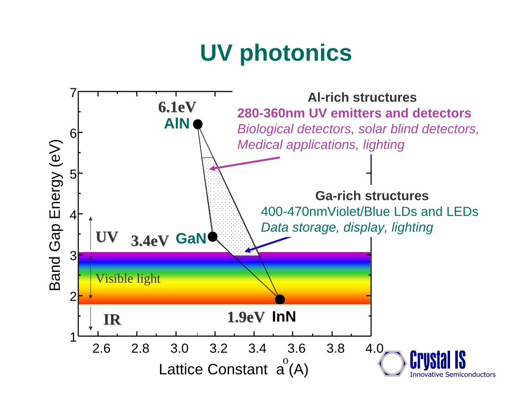
UV photonics
2.6 2.8 3.0 3.2 3.4 3.6 3.8 4.01
2
3
4
5
6
7
o
InN
GaN
AlN
Ban
d G
ap E
nerg
y (e
V)
Lattice Constant a (A)
Visible light
UVUV
IRIR 1.9eV1.9eV
3.4eV3.4eV
6.1eV6.1eV Al-rich structures280-360nm UV emitters and detectorsBiological detectors, solar blind detectors,Medical applications, lighting
400-470nmViolet/Blue LDs and LEDsData storage, display, lighting
Ga-rich structures
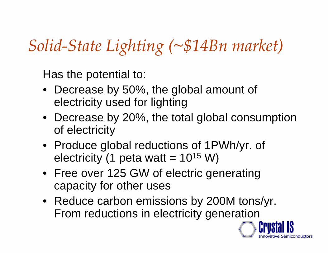
Solid-State Lighting (~$14Bn market)Has the potential to:• Decrease by 50%, the global amount of
electricity used for lighting• Decrease by 20%, the total global consumption
of electricity• Produce global reductions of 1PWh/yr. of
electricity (1 peta watt = 1015 W)• Free over 125 GW of electric generating
capacity for other uses• Reduce carbon emissions by 200M tons/yr.
From reductions in electricity generation

Laser Diode Market
•Optical Data Storage Market will use over 300M LDs in 1999 (Compound Semicond., March 1999)
•HD-DVD will use GaN or SHG laser; will dominate future market with 27GB capacity (single-sided, single-layer) or greater (Currently 5GB; 20 to 30 GB needed for 2hrs. of HD television video.)•Market expects laser cost to be approx. $10.
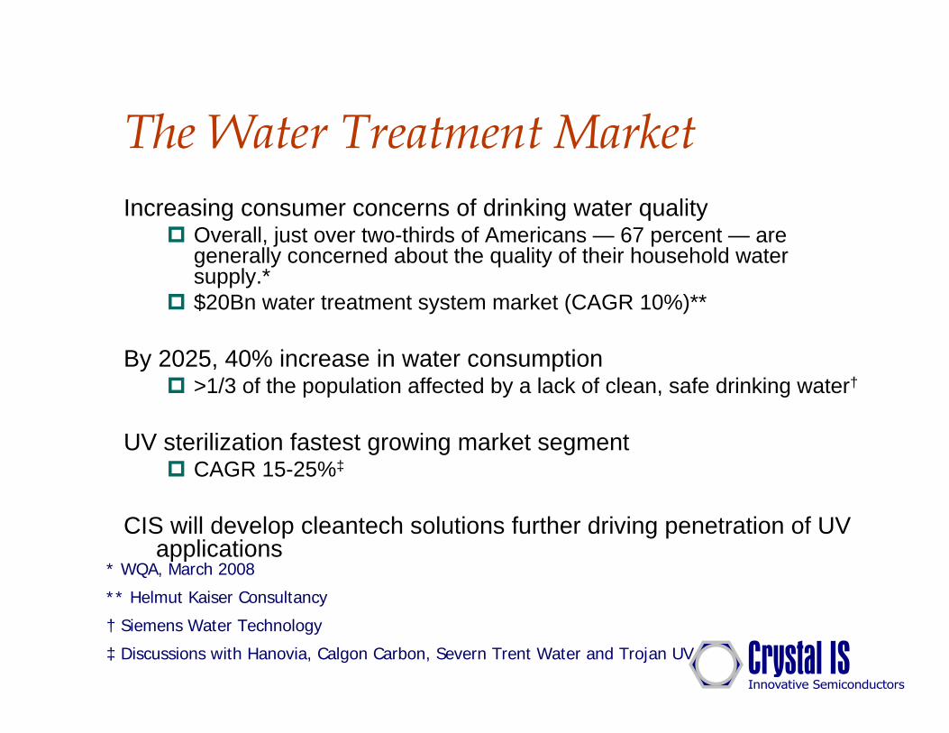
Increasing consumer concerns of drinking water qualityOverall, just over two-thirds of Americans — 67 percent — are generally concerned about the quality of their household water supply.*$20Bn water treatment system market (CAGR 10%)**
By 2025, 40% increase in water consumption >1/3 of the population affected by a lack of clean, safe drinking water†
UV sterilization fastest growing market segment CAGR 15-25%‡
CIS will develop cleantech solutions further driving penetration of UV applications
* WQA, March 2008
** Helmut Kaiser Consultancy
† Siemens Water Technology
‡ Discussions with Hanovia, Calgon Carbon, Severn Trent Water and Trojan UV
The Water Treatment Market
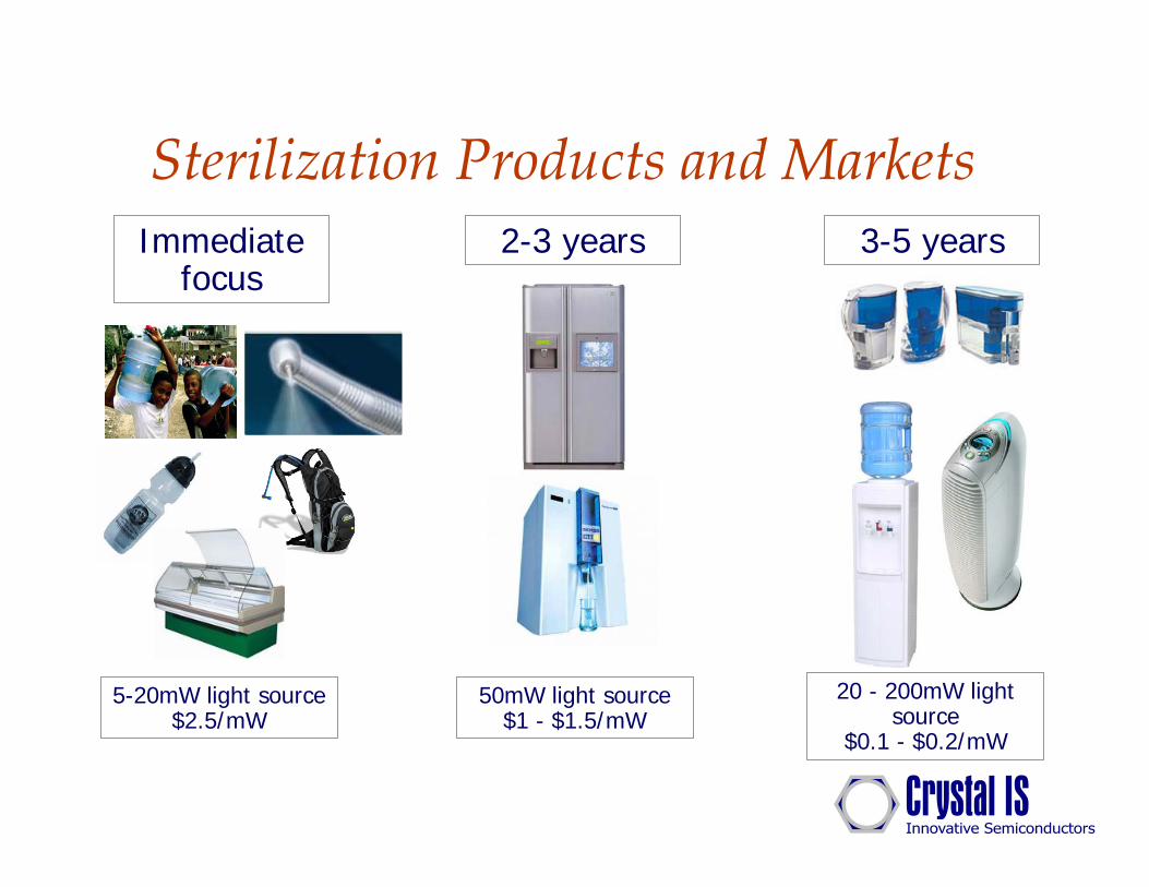
Sterilization Products and MarketsImmediate
focus2-3 years 3-5 years
5-20mW light source$2.5/mW
50mW light source$1 - $1.5/mW
20 - 200mW light source
$0.1 - $0.2/mW

UV-C LEDs for Disinfection
265nm is the optimum wavelength for disinfection
AlN is the optimum substrate for devices working at this wavelength
Only AlN based LEDs will work at the powers needed
DNA and RNA disabled by UV-C

What is a semiconductor?Metals
Many free electrons not tied up in chemical bonds
InsulatorsAll electrons (in intrinsic material) tied up in chemical bonds

Atoms
Electrons can absorb energy and move to a higher levelWhite light (all colors combined) passing through a gas will come out missing certain wavelengths (absorption spectrum)
Electrons can emit light and move to a lower levelCalculating the allowed energies extremely complicated for
anything with more than one electronBut can deduce allowed energies from light that is emitted
E=0 (unbound)
n=1
n=2n=3n=4
Really eight closely spaced energies, since no two electrons can occupy same state

Atomic BondingElectrons in an unfilled valence shell are loosely boundAtoms will form bonds to fill valence shells, either by sharing
valence electrons, borrowing them, or loaning themWhen atoms bond in solids, sharing electrons, each atom’s energy
levels get slightly shifted
E=0 (unbound)
n=1
n=2n=3n=4

Crystal (Perfect)

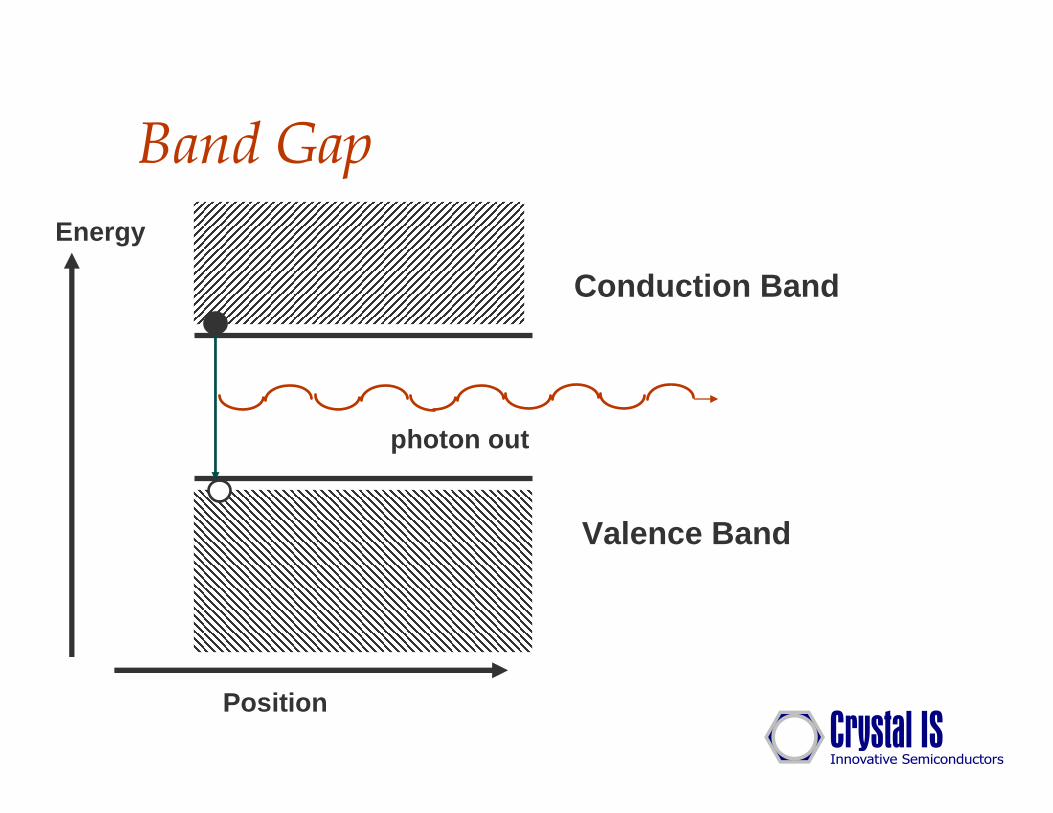
Band Gap
Valence Band
Conduction Band
Band Gap Energy Eg(Minimum Energy needed tobreak the chemical bonds)
Energy
Position

Crystal (Excited)

Crystal (Excited)

Band Gap
Valence Band
Conduction Band
Band Gap Energy Eg(Minimum Energy needed tobreak the chemical bonds)
Energy
Position

Band Gap
Valence Band
Conduction Band
Energy
Position
photonin h Egν =
Band Gap
Valence Band
Conduction Band
Energy
Position
photon out

Band Gap
Valence Band
Conduction Band
Energy
Position
photon out

Crystal (Doped n-type)
+5

Crystal (Doped p-type)
+3

Doped SemiconductorsEnergy
n-type p-type
donor level
acceptor level
Put them together?

p-n junction
n-type
p-type
Energy
depleted region(electric field)
+ + + + + ++
+-------
-

p-n junction
n-type
p-type
Energy
depleted region(electric field)
+ + + + + ++
+-------
-
Vo

What happens if a voltage is applied?
By adding a battery for instance.
The voltage applied causes the junction to change – to have a “bias”

Biased junction
n-type
p-type
depleted region(electric field)
Negativebias
positivebias

Biased junction
n-type
p-type
depleted region(electric field)
Negativebias
photon out

Light-emitting Diode (LED)
First visible LED
Blue LED

Traffic Lights
One of the first applications of the new nitride semiconductor technology. The Green light uses 10% of the power and last more than 10x longer.

The Promise
280 290 300 310 320
PL In
tens
ity (a
.u.)
Wavelength(nm)
LED on AlN
LED onsapphire
AFM of AlN grown on sapphire substrates with
defects ~109/cm2
AFM of AlGaN grown on AlN substrates with
defects ~104/cm2
•Dislocations in substrate < 104 cm-2
•Pseudomorphic LED structures retain low dislocation density
•Apparent x10 PL improvement should translate into improved LED efficiency

LED structure

STEM of Device Structure
20nm
High-angle annular dark field (HAADF) image which shows Z contrast (higher Ga concentration appears lighter). Pseudomorphic growth allows a high quality structure to be grown.


HistoryFounded in 1997 from RPI
Focused SBIR and DARPA contracts for AlN substrate development ($10M in Federal Contracts/Grants)
VC Funded with $15.6M in two rounds (Sept 2004 and Aug 2006)
Refocus business to commercialize substrates and develop Deep UV LEDs and Laser Diodes
Released World’s first 2-inch single-crystal AlN substrate, cut from a bulk boule, in May 2006
Demonstrated devices at 255 – 340nmEfficiencies need to be improved
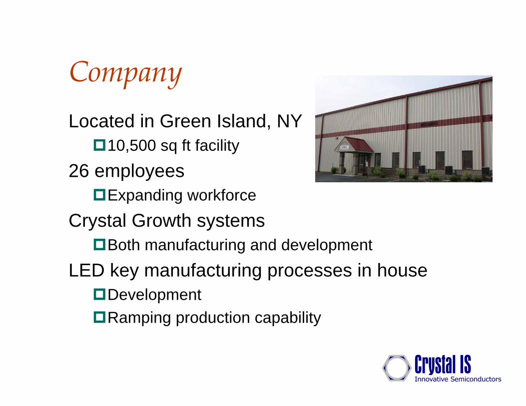
CompanyLocated in Green Island, NY
10,500 sq ft facility26 employees
Expanding workforceCrystal Growth systems
Both manufacturing and developmentLED key manufacturing processes in house
DevelopmentRamping production capability

Value Proposition
World’s lowest defect III-N Crystals from native bulk growth
HighPerformance
UV LEDs
2-inch substrate preparation Internal LED
manufacturing


LED fabrication flowchart
Epi-structure design –
this is the structure that
defines the LED
Epi-wafer
MOVPE growth of the structure
Packaged LED deviceProcessed wafer
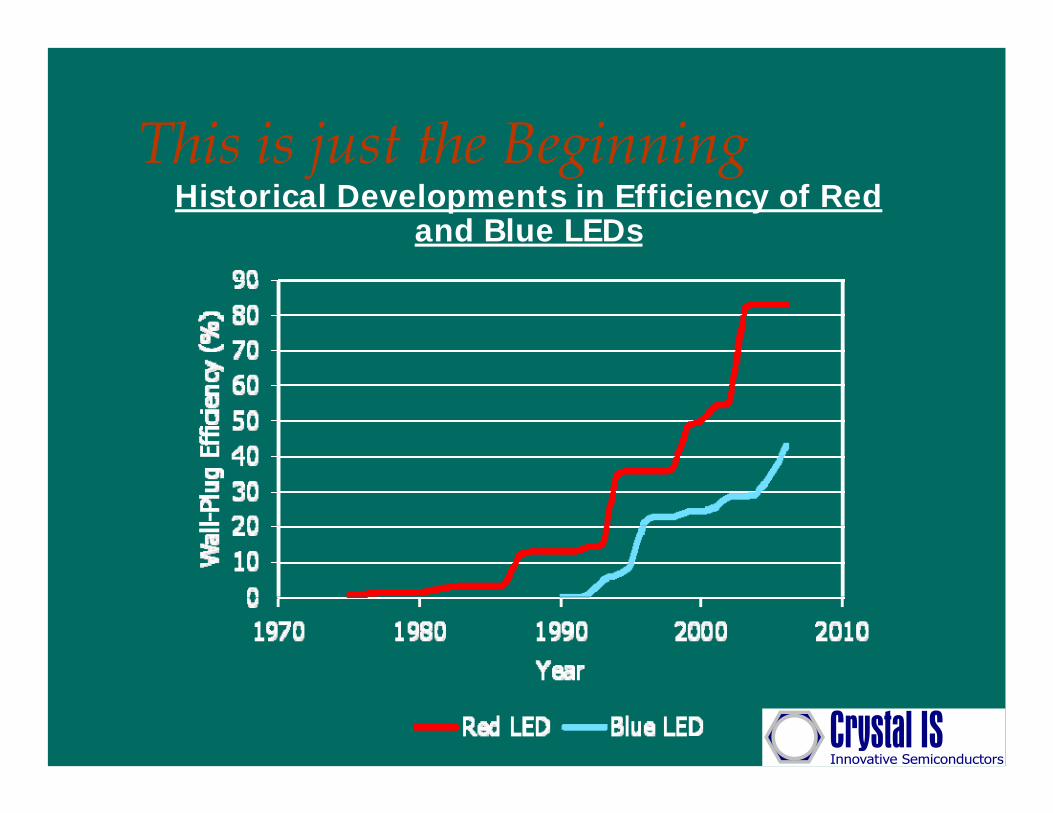
This is just the Beginning Historical Developments in Efficiency of Red
and Blue LEDs

Deep UV LEDs will Follow a Similar Technology Roadmap
Efficiency Forecast for Deep UV LEDs(based on 280nm LED)

Price Improvements as the Technology Matures
Price Forecast for Deep UV LEDs(based on 280nm LED)

AlN grown on sapphire
Because the AlN LED structure has a different atomic lattice than the sapphire substrate, dislocations occur as shown above
Dislocations limit performance of the LED and degrade its lifetime significantly
AlN layer on sapphire has ~100,000,000 dislocations per cm2. The vertical black lines in the right hand image are dislocations in the AlN layer on sapphire.
AlN layers on Crystal IS native substrates have ~1,000 dislocations per cm2

The importance of the substrateMost LEDs today are manufactured on sapphire
substratesThis is OK for visible LEDs, but presents a problem for UV LEDsUVA LEDs are commercially (from Japan) available down to 365nm
• Significant drop in efficiency from blue LEDs due to high defect density
UVB LEDs are available at low efficiency (~1%) and have lifetimes (to 50% of original intensity) on the order of 1,000 hours
Crystal IS is developing its LEDs on low defect AlN to address these problems

What are the hot research topics?Quantum ConfinementDoping wide bandgaps (p-type doping)Piezo-electric fieldsRadiative vs non-radiative recombination
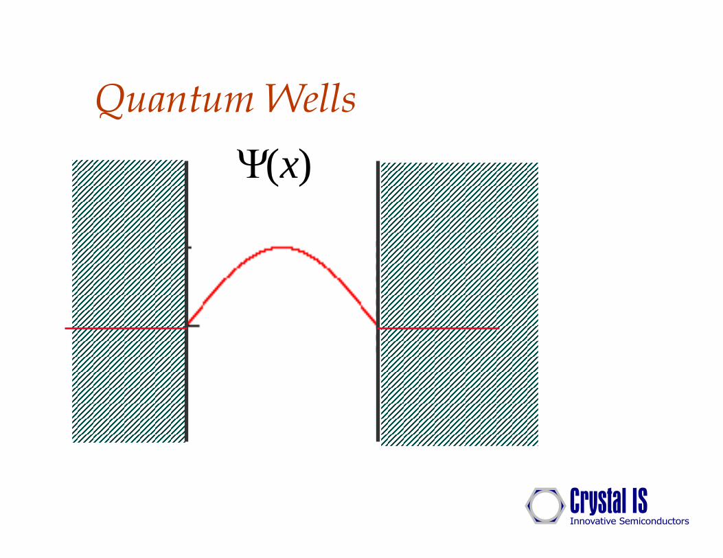
Quantum WellsΨ( )x

Quantum MechanicsProbability density given by
Schroedinger’s Equation:
where
Ψ( )x 2
− = −∂∂
2
2xx C E U xΨ Ψ( ) ( ) ( )
C mh
=16 2
2
π

Quantum Mechanics (cont.)Main point is that energy levels are Quantized!
Well defined energy level even at room temperature.

Energy Band Diagram
n-co
ntac
t lay
er
MQ
W
bloc
king
laye
r p-
cont
act l
ayer
p-G
aN
QWs strongly deformed by built-in polarization => small LED efficiency

Radiative Recombinationvertical profile spectrum
QW band-gap adjustment will move peak to 280 nm

Non-radiative Recombinationvertical profile
lifetime = 10nsprobably too long(typical: 1ns)

ConclusionsVery intense and fast moving field
Physicists are making major contributions(including starting new businesses)
Quantum Mechanics plays a major role in semiconductor physics these days.
Lots more to do