Ultrasonic Soldering for Structural Electronic Applications
13
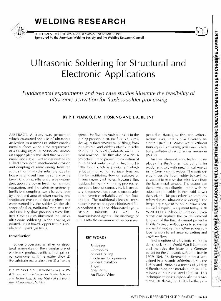
/ WELDING RESEARCH SUPPLEMENT TO THE WELDING JOURNAL, NOVEMBER 1996 Sponsored by the American Welding Society and the Welding ResearchCouncil Ultrasonic Soldering for Structural Electronic Applications and Fundamental experiments and two case studies illustrate the feasibility of ultrasonic activation for fluxless solder processing BY P. T. VIANCO, F. M. HOSKING AND J. A. REJENT ABSTRACT. A study was performed which examined the use of uhrasonic activation as a means of solder coating metal surfaces without the requirement of a fluxing agent. Fundamental studies on copper plates revealed that oxide re- moval and subsequent solder wetting re- sulted from both mechanical erosion and coupling of sonic energy from the source (horn) into the substrate. Cavita- tion was removed from the surface oxide layer. Coupling efficiency was depen- dent upon the power level, horn sample separation, and the substrate geometry. Inefficient coupling was characterized by a reduced area of solder coating and significant erosion of those regions that were wetted by the solder. In the ab- sence of a flux, traditional meniscus rise and capillary flow processes were lini- ited. Case studies illustrated the use of ultrasonic soldering in the coating of printed c ircu it board copper features and electronic package leads. Introduction Solder processing, whether for struc- tural assemblies or the manufacture of electronic products, utilizes three princi- pal components: 1) the solder alloy, 2) the substrate material(s), and 3) a fluxing f~ I: VIANCO, I~ M. HOSKING and J. A. RE- JENT are with the Center for Solder Science and Technology, Sandia National Laborato- ries, Albuquerque, N. Mex. agent. The flux has multiple roles in the joining process. First, the flux is a corro- sive agent that removes oxide film(s) from the substrate and solder surfaces, thereby promoting the solder/substrate metallur- gical reaction. The flux also provides a protective film to prevent re-oxidation of the (:leaned surfaces upon heating. Fi- nally, the flux acts as a surfactant which reduces the solder surface tension, thereby facilitating flow on surfaces or through gaps and holes. Because flux residues left by the soldering process re- tain some level of corrosivity, it is neces- sary to remove them so as to ensure ade- quate service reliability of the final product. The traditional cleaning tech- niques have relied upon chlorinated flu- orocarbon (CFC) and chlorinated hydro- carbon solvents as well as aqueous-based agents. The discharge of CFCs into the environment has been sus- KEY W O R D S Soldering Ultrasonics Solder Coating Electronic Components Solder Cavitation 100Sn 60Sn-40Pb Au-Plated Wires pected of damaging the stratospheric ozone layer, and is now severely re- stricted (Ref. 1). Waste water effluent from aqueous cleaning processes poten- tially pollutes drinking water resources (Ref. 2). An alternative soldering technique re- places the flux's chemical activity for oxide removal, with mechanical energy in the form of sound waves. The sonic en- ergy forces the liquid solder to cavitate, causing it to remove the oxide layer from the base metal surface. The solder can then form a metallurgical bond with the substrate; the solder is then said to wet the surface. This procedure is conlmonly referred to as "ultrasonic soldering." The frequency range of the sound waves gen- erated by typical equipment today is 20 to 20,000 Hz. Although ultrasonic exci- tation can replace the oxide removal function of the flux, it cannot protect a freshly cleaned surface prior to soldering nor will it modify the molten solder sur- face tension to enhance spreading and capillary flow. First mention of ultrasonic soldering dates back to pre-World War II Germany and includes the issue of a German patent for the ultrasonic soldering iron in 1939 (Ref. 3). Renewed interest was gained in ultrasonic soldering during the 1950s and 1960s as a means of joining difficult-to-solder metals such as alu- minum or stainless steel (Ref. 4). This technique received large-scale manufac- turing use during the 1970s for the join- WELDING RESEARCH SUPPLEMENT I 343-s
Transcript of Ultrasonic Soldering for Structural Electronic Applications
/
W E L D I N G R E S E A R C H
SUPPLEMENT TO THE WELDING JOURNAL, NOVEMBER 1996 Sponsored by the American Welding Society and the Welding Research Council
Ultrasonic Soldering for Structural Electronic Applications
and
Fundamental experiments and two case studies illustrate the feasibility of ultrasonic activation for fluxless solder processing
BY P. T. V I A N C O , F. M. H O S K I N G A N D J. A. REJENT
ABSTRACT. A study was performed which examined the use of uhrasonic activation as a means of solder coating metal surfaces without the requirement of a f luxing agent. Fundamental studies on copper plates revealed that oxide re- moval and subsequent solder wetting re- sulted from both mechanical erosion and coupling of sonic energy from the source (horn) into the substrate. Cavita- tion was removed from the surface oxide layer. Coupl ing eff iciency was depen- dent upon the power level, horn sample separation, and the substrate geometry. Inefficient coupl ing was characterized by a reduced area of solder coating and significant erosion of those regions that were wetted by the solder. In the ab- sence of a flux, traditional meniscus rise and capil lary f low processes were l ini- ited. Case studies illustrated the use of ultrasonic soldering in the coating of printed c ircu it board copper features and electronic package leads.
Introduction
Solder processing, whether for struc- tural assemblies or the manufacture of electronic products, utilizes three princi- pal components: 1) the solder alloy, 2) the substrate material(s), and 3) a f luxing
f~ I: VIANCO, I~ M. HOSKING and J. A. RE- JENT are with the Center for Solder Science and Technology, Sandia National Laborato- ries, Albuquerque, N. Mex.
agent. The flux has multiple roles in the joining process. First, the flux is a corro- sive agent that removes oxide film(s) from the substrate and solder surfaces, thereby promoting the solder/substrate metallur- gical reaction. The flux also provides a protective film to prevent re-oxidation of the (:leaned surfaces upon heating. Fi- nally, the flux acts as a surfactant which reduces the solder surface tension, thereby facilitating f low on surfaces or through gaps and holes. Because f lux residues left by the soldering process re- tain some level of corrosivity, it is neces- sary to remove them so as to ensure ade- quate service re l iabi l i ty of the f inal product. The traditional cleaning tech- niques have relied upon chlorinated flu- orocarbon (CFC) and chlorinated hydro- carbon solvents as wel l as aqueous-based agents. The discharge of CFCs into the environment has been sus-
KEY WORDS
Soldering Ultrasonics Solder Coating Electronic Components Solder Cavitation 100Sn 60Sn-40Pb Au-Plated Wires
pected of damaging the stratospheric ozone layer, and is now severely re- stricted (Ref. 1). Waste water effluent from aqueous cleaning processes poten- tially pollutes drinking water resources (Ref. 2).
An alternative soldering technique re- places the flux's chemical activity for oxide removal, with mechanical energy in the form of sound waves. The sonic en- ergy forces the l iquid solder to cavitate, causing it to remove the oxide layer from the base metal surface. The solder can then form a metallurgical bond with the substrate; the solder is then said to wet the surface. This procedure is conlmonly referred to as "ultrasonic soldering." The frequency range of the sound waves gen- erated by typical equipment today is 20 to 20,000 Hz. Although ultrasonic exci- tation can replace the oxide removal function of the flux, it cannot protect a freshly cleaned surface prior to soldering nor wi l l it modify the molten solder sur- face tension to enhance spreading and capillary flow.
First mention of ultrasonic soldering dates back to pre-World War II Germany and includes the issue of a German patent for the ultrasonic soldering iron in 1939 (Ref. 3). Renewed interest was gained in ultrasonic soldering during the 1950s and 1960s as a means of joining di f f icul t - to-solder metals such as alu- minum or stainless steel (Ref. 4). This technique received large-scale manufac- turing use during the 1970s for the join-
W E L D I N G RESEARCH SUPPLEMENT I 343-s
Sample Holde_~.
Sample Ultrasonic (front)
H°rn._ . . . . . . . . . . . . . . L
~ . Solder . . . . . . . . . . . . . . /E / ,,,,Lo,,e,
. " . / / . / •
PARAMETERS A - horn-sample separation B - horn vertical position C - immersion dimension t - sample thickness L - sample dimensions e - horn-sample vertical
rotation
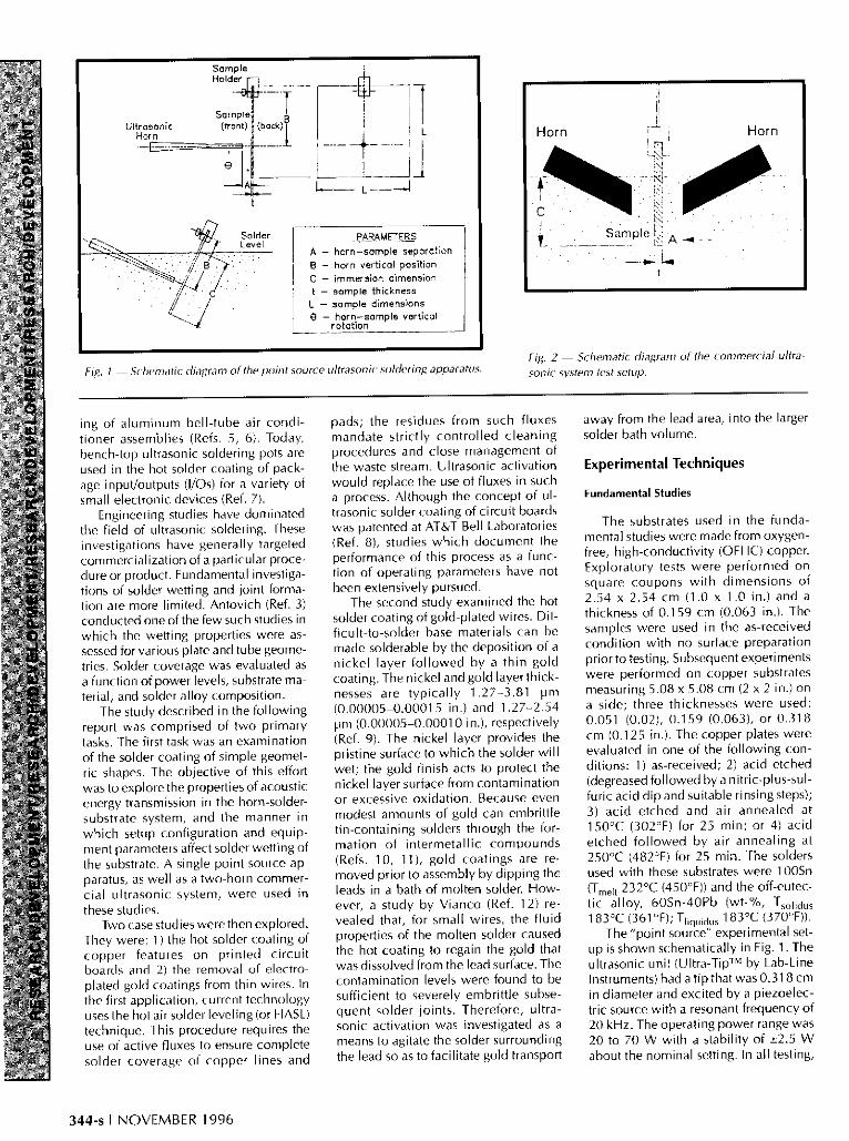
Fig. 1 - - Schematic diagram of the point source ultrasonic soldering apparatus.
Horn Horn
C
i , Sample ~ ! . . . . .
- , , . - ~ .......
t
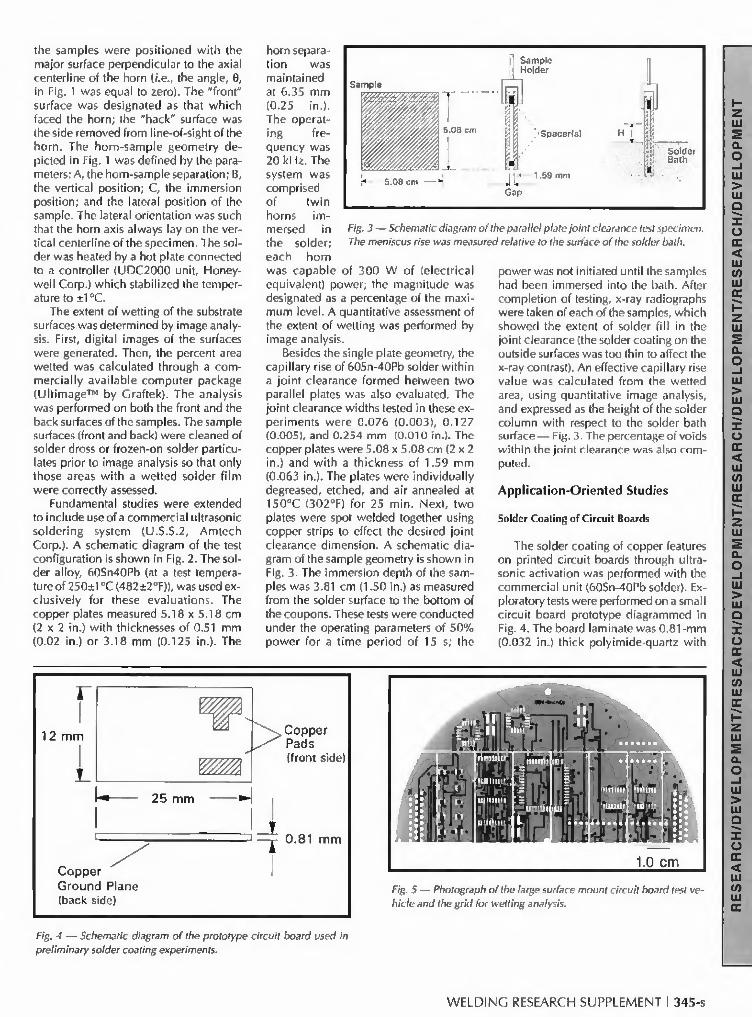
Fig. 2 - - Schematic diagram of the commercial ultra-
sonic system test setup.
ing of aluminum bell-tube air condi- tioner assemblies (Refs. 5, 6). Today, bench-top ultrasonic soldering pots are used in the hot solder coating of pack- age input/outputs (I/as) for a variety of small electronic devices (Ref. 7).
Engineering studies have dominated the field of ultrasonic soldering. These investigations have generally targeted commercialization of a particular proce- dure or product. Fundamental investiga- tions of solder wetting and joint forma- tion are more limited. Antovich (Ref. 3) conducted one of the few such studies in which the wetting properties were as- sessed for various plate and tube geome- tries. Solder coverage was evaluated as a function of power levels, substrate ma- terial, and solder alloy composition.
The study described in the following report was comprised of two primary tasks. The first task was an examination of the solder coating of simple geomet- ric shapes. The objective of this effort was to explore the properties of acoustic energy transmission in the horn-solder- substrate system, and the manner in which setup configuration and equip- ment parameters affect solder wetting of the substrate. A single point source ap- paratus, as well as a two-horn commer- cial ultrasonic system, were used in these studies.
Two case studies were then explored. They were: 1) the hot solder coating of copper features on printed circuit boards and 2) the removal of electro- plated gold coatings from thin wires. In the first application, current technology uses the hot air solder leveling (or HASL) technique. This procedure requires the use of active fluxes to ensure complete solder coverage of copper lines and
pads; the residues from such fluxes mandate strictly controlled cleaning procedures and close management of the waste stream. Ultrasonic activation would replace the use of fluxes in such a process. Although the concept of ul- trasonic solder coating of circuit boards was patented at AT&T Bell Laboratories (Ref. 8), studies which document the performance of this process as a func- tion of operating parameters have not been extensively pursued.
The second study examined the hot solder coating of gold-plated wires. Dif- ficult-to-solder base materials can be made solderable by the deposition of a nickel layer followed by a thin gold coating. The nickel and gold layer thick- nesses are typically 1.27-3.81 IJm (0.00005-0.00015 in.) and 1.27-2.54 pm (0.00005-0.00010 in.), respectively (Ref. 9). The nickel layer provides the pristine surface to which the solder will wet; the gold finish acts to protect the nickel layer surface from contamination or excessive oxidation. Because even modest amounts of gold can embrittle tin-containing solders through the for- mation of intermetallic compounds (Refs. 10, 11), gold coatings are re- moved prior to assembly by dipping the leads in a bath of molten solder. How- ever, a study by Vianco (Ref. 12) re- vealed that, for small wires, the fluid properties of the molten solder caused the hot coating to regain the gold that was dissolved from the lead surface. The contamination levels were found to be sufficient to severely embrittle subse- quent solder joints. Therefore, ultra- sonic activation was investigated as a means to agitate the solder surrounding the lead so as to facilitate gold transport
away from the lead area, into the larger solder bath volume.
Experimental Techniques
Fundamental Studies
The substrates used in the funda- mental studies were made from oxygen- free, high-conductivity (OFHC) copper. Exploratory tests were performed on square coupons with dimensions of 2.54 x 2.54 cm (1.0 x 1.0 in.) and a thickness of 0.159 cm (0.063 in.). The samples were used in the as-received condition with no surface preparation prior to testing. Subsequent experiments were performed on copper substrates measuring 5.08 x 5.08 cm (2 x 2 in.) on a side; three thicknesses were used: 0.051 (0.02), 0.159 (0.063), or 0.318 cm (0.125 in.). The copper plates were evaluated in one of the following con- ditions: 1) as-received; 2) acid etched (degreased followed by a nitric-plus-sul- furic acid dip and suitable rinsing steps); 3) acid etched and air annealed at 150°C (302°F) for 25 min; or 4) acid etched followed by air annealing at 250°C (482°F) for 25 min. The solders used with these substrates were 100Sn (Tmelt 232°C (450°F)) and the off-eutec- tic alloy, 60Sn-40Pb (wt-%, Tsolidu s 183°C (361 °F); Tliquidus 183°C (370°F)).
The "point source" experimental set- up is shown schematically in Fig. 1. The ultrasonic unit (Ultra-Tip TM by Lab-Line Instruments) had a tip that was 0.318 cm in diameter and excited by a piezoelec- tric source with a resonant frequency of 20 kHz. The operating power range was 20 to 70 W with a stability of _+2.5 W about the nominal setting. In all testing,
344-s I NOVEMBER 1996
the samples were positioned with the major surface perpendicular to the axial centerline of the horn (i.e., the angle, e, in Fig. 1 was equal to zero). The "front" surface was designated as that which faced the horn; the "back" surface was the side removed from line-of-sight of the horn. The horn-sample geometry de- picted in Fig. 1 was defined by the para- meters: A, the horn-sample separation; B, the vertical position; C, the immersion position; and the lateral position of the sample. The lateral orientation was such that the horn axis always lay on the ver- tical centerline of the specimen. The sol- der was heated by a hot plate connected to a controller (UDC2000 unit, Honey- well Corp.) which stabilized the temper- ature to +1 °C.
The extent of wetting of the substrate surfaces was determined by image analy- sis. First, digital images of the surfaces were generated. Then, the percent area wetted was calculated through a com- mercially available computer package (Ultimage TM by Graftek). The analysis was performed on both the front and the back surfaces of the samples. The sample surfaces (front and back) were cleaned of solder dross or frozen-on solder particu- lates prior to image analysis so that only those areas with a wetted solder film were correctly assessed.
Fundamental studies were extended to include use of a commercial ultrasonic soldering system (U.S.S.2, Amtech Corp.). A schematic diagram of the test configuration is shown in Fig. 2. The sol- der alloy, 60Sn40Pb (at a test tempera- ture of 250±I °C (482±2°F)), was used ex- clusively for these evaluations. The copper plates measured 5.18 x 5.18 cm (2 x 2 in.) with thicknesses of 0.51 mm (0.02 in.) or 3.18 mm (0.125 in.). The
horn separa-
S i a m p l e i~l'~ .: . . tion was Holder maintained Sample at 6.35 mm T . . . . . . (0.25 in.). ~ - / - ~ The operat- ~ / / / ~ , / ~ l ing fre- 5.08 cm i 'Spacer(s)
quencywas ..: : : i i : " ;i. 2 0 k H z . T h e u, 'Jl l / / / l l l l l l l l l f , ,~ _ L . . . . . . L~SI_~.! .59 mm : : s y s t e m w a s ~---- 5 .08 cm ~ _ _ ~ " ":C " - • comprised Gap of twin horns im- mersed in Fig. 3 - - Schematic diagram of the parallel plate joint clearance test specimen. the solder; The meniscus rise was measured relative to the surface of the solder bath. each horn was capable of 300 W of (electrical equivalent) power; the magnitude was designated as a percentage of the maxi- mum level. A quantitative assessment of the extent of wetting was performed by image analysis.
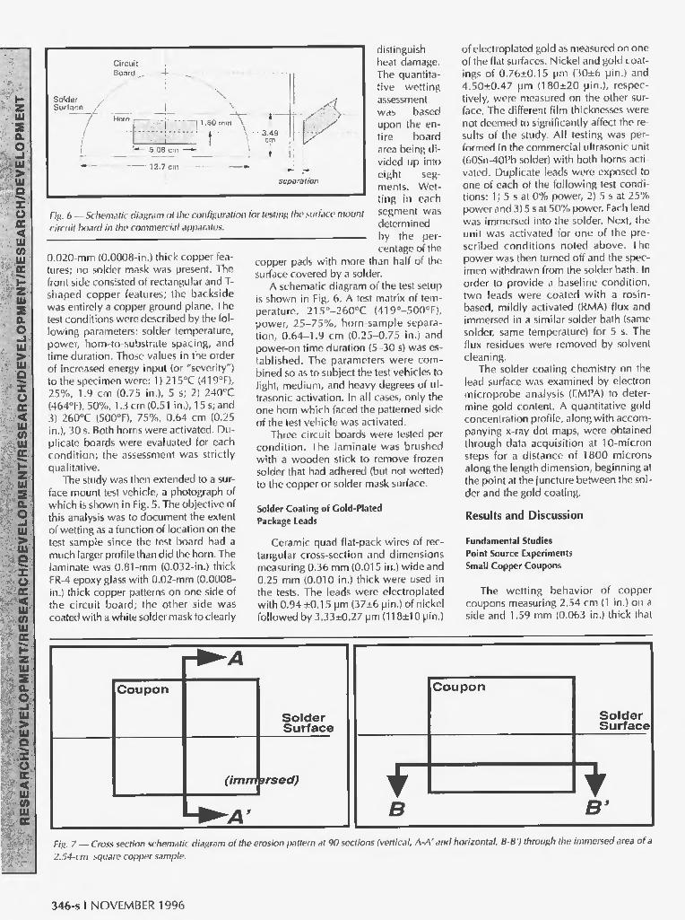
Besides the single plate geometry, the capillary rise of 60Sn-40Pb solder within a joint clearance formed between two parallel plates was also evaluated. The joint clearance widths tested in these ex- periments were 0.076 (0.003), 0.127 (0.005), and 0.254 mm (0.010 in.). The copper plates were 5.08 x 5.08 cm (2 x 2 in.) and with a thickness of 1.59 mm (0.063 in.). The plates were individually degreased, etched, and air annealed at 150°C (302°F) for 25 min. Next, two plates were spot welded together using copper strips to effect the desired joint clearance dimension. A schematic dia- gram of the sample geometry is shown in Fig. 3. The immersion depth of the sam- ples was 3.81 cm (1.50 in.) as measured from the solder surface to the bottom of the coupons. These tests were conducted under the operating parameters of 50% power for a time period of 15 s; the
power was not initiated until the samples had been immersed into the bath. After completion of testing, x-ray radiographs were taken of each of the samples, which showed the extent of solder fill in the joint clearance (the solder coating on the outside surfaces was too thin to affect the x-ray contrast). An effective capillary rise value was calculated from the wetted area, using quantitative image analysis, and expressed as the height of the solder column with respect to the solder bath surface - - Fig. 3. The percentage of voids within the joint clearance was also com- puted.
Application-Oriented Studies
Solder Coating of Circuit Boards
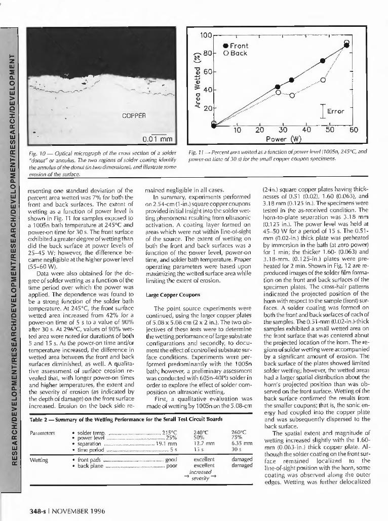
The solder coating of copper features on printed circuit boards through ultra- sonic activation was performed with the commercial unit (60Sn-40Pb solder). Ex- ploratory tests were performed on a small circuit board prototype diagrammed in Fig. 4. The board laminate was 0.81-mm (0.032 in.) thick polyimide-quartz with
12 mm
25 mm
J Copper Ground Plane (back side)
Copper Pads (front side)
--~ 0.81 mm
. - ~ ~ "'11 ". ~
/:-., t .
S.l il Pt.t ! ! . . , • i t ° i . il
e F<+- I : ] 7 .7i ,
1.0 c m
Fig. 5 - - Photograph of the large surface mount circuit board test ve- hicle and the grid for wetting analysis.
Fig. 4 - - Schematic diagram of the prototype circuit board used in preliminary solder coating experiments.
WELDING RESEARCH SUPPLEMENT I 345-s
Circuit Board .... t . . . . . . . . .
S o l d e r ~
Surfact ~- / I "" .......... ~ ' ~ ........ I ............. z, Horn 1.60 mm ' j
/ " i! . . . . >", 3.49cm
........... 1 2.7 cm " - -~ separa t/of?
distinguish heat damage. The quantita- tive wett ing assessment was based upon the en- tire board area being di- vided up into eight seg- ments. Wet- ting in each
FiR. 6 - - Schematic dia,qram o f the confi,~uration for testin~ the surface mount
circuit board in the commerc ia l apparatus.
segment was determined by the per-
0.020-mnl (0.0008-in.) thick copper fea- tures; no solder mask was present. The front side consisted of rectangular and T- shaped copper features; the backside was entirely a copper ground plane. The test conditions were described by the fol- lowing parameters: solder temperature, power, horn-to-substrate spacing, and time duration. Those values in the order of increased energy input (or "severity") to the specimen were: 1) 215°C (419°F), 25%, 1.9 crn (0.75 in.), 5 s; 2) 240°C (464°F), 50%, 1.3 cm (0.51 in.), 15 s; and 3) 260°C (500°F), 75%, 0.64 cm (0.25 in.), 30 s. Both horns were activated. Du- plicate boards were evaluated for each condit ion; the assessment was strictly qualitative.
The study was then extended to a sur- face mount test vehicle, a photograph of which is shown in Fig. 5. The objective of this analysis was to document the extent of wetting as a function of location on the test sample since the test board had a much larger profile than did the horn. The laminate was 0.81-mm (0.032-in.) thick FR-4 epoxy glass with 0.02-mm (0.0008- in.) thick copper patterns on one side of the circuit board; the other side was coated with a white solder mask to clearly
centage of the copper pads with more than half of the surface covered by a solder.
A schematic diagram of the test setup is shown in Fig. 6. A test matrix of tem- perature, 215°-260°C (419°-500°F), power, 25-75%, horn-sample separa- tion, 0.64-1.9 cm (0.25-0.75 in.) and power-on time duration (5-30 s) was es- tablished. The parameters were com- bined so as to subject the test vehicles to light, medium, and heavy degrees of ul- trasonic activation. In all cases, only the one horn which faced the patterned side of the test vehicle was activated.
Three circuit boards were tested per condit ion. The laminate was brushed with a wooden stick to remove frozen solder that had adhered (but not wetted) to the copper or solder mask surface.
Solder Coating of Gold-Plated Package Leads
Ceramic quad flat-pack wires of rec- tangular cross-section and dimensions measuring 0.36 mm (0.015 in.) wide and 0.25 mm (0.010 in.) thick were used in the tests. The leads were electroplated with 0.94 +0.15 IJm (37_+6 IJin.) of nickel fol lowed by 3.33___0.27 tJm (118-+10 lain.)
of electroplated gold as measured on one of the flat surfaces. Nickel and gold coat- ings of 0.76+_0.15 IJm (30_+6 ~ain.) and 4.50_+0.47 pm (1 80+_20 pin.), respec- tively, were measured on the other sur- face. The different film thicknesses were not deemed to significantly affect the re- sults of the study. All testing was per- formed in the commercial ultrasonic unit (60Sn-40Pb solder) with both horns acti- vated. Duplicate leads were exposed to one of each of the fol lowing test condi- tions: 1) 5 s at 0% power, 2) 5 s at 25% power and 3) 5 s at 50% power. Each lead was immersed into the solder. Next, the unit was activated for one of the pre- scribed condit ions noted above. The power was then turned off and the spec- imen withdrawn from the solder bath. In order to provide a baseline condit ion, two leads were coated with a rosin- based, mildly activated (RMA) flux and immersed in a similar solder bath (same solder, same temperature) for 5 s. The flux residues were removed by solvent cleaning.
The solder coating chemistry on the lead surface was examined by electron microprobe analysis (EMPA) to deter- mine gold content. A quantitative gold concentration profile, along with accom- panying x-ray dot maps, were obtained through data acquisition at 10-micron steps for a distance of 1800 microns along the length dimension, beginning at the point at the juncture between the sol- der and the gold coating.
Results and Discussion
Fundamental Studies Point Source Experiments Small Copper Coupons
The wett ing behavior of copper coupons measuring 2.54 cm (1 in.) on a side and 1.59 mm (0.063 in.) thick that
C o u p o n
(imrn
I- A,
S o l d e r S u r f a c e
=.rsed)
B I
S o l d e r S u r f a c e
B"
Fig. 7 - - Cross section schematic diagram o f the erosion pattern at 90 sections (vertical, A-A ' and horizontal, B-B') through the immersed area o f a
2.54-cm square copper sample.
346-s I NOVEMBER 1996

Table 1 - - Percent Area Wetted (left or right) of Copper Specimens Using 60Sn-40Pb Solder and the Commercial Ultrasonic Unit
Sample Thickness (ram) Horn
0.51 both
0.51 right only
3.18 both
3.18 right only
were exposed to the point source of ul- trasonic energy, provided the initial, ex- ploratory data. The values of A, B, and C for the horn/sample geometry (Fig. 1) were 3.18 mm (0.125 in.), 14.2 mm (0.559 in.), and 36.6 mm (1.44 in.), re- spectively. It was observed that a solder film had formed on both the front and back surfaces of the coupons after ultra- sonic activation. Also, the wetted area extended wel l beyond the projected footprint of the horn (i.e., a 3.18-mm (0.125-in.) diameter circle for either test condit ion. Both observations indicated that oxide removal and solder wetting were not due entirely to the erosion gen- erated by cavitation of the liquid solder between the horn and the substrate sur- face. Rather, sonic energy appeared to couple to the copper coupon and then be available to all of the surfaces. These re- sults suggest that ultrasonic activation wi l l depend as strongly upon the bulk properties of the specimen material as on its surface condition or the operating pa- rameters of the source.
Significant erosion took place on the front surface of the specimen (i.e., the surface which faced the ultrasonic horn). Shown in Fig. 7 are two schematic dia- grams. In each of views (a) and (b), a hor- izontal line represents the location of the solder surface at the time of testing. Ver- tical and horizontal sections are show as A-A' and B-B,' respectively. A schematic of each section is illustrated at the bottom of each diagram. The case of the vertical cross-sectional view of a typical sample front surface fol lowing exposure to the ultrasonic horn is shown in (a). An abrupt thickness change was observed along the vertical section of the sample; the point of transition was the solder bath free sur- face. An optical micrograph (Fig. 8) of the same cross section from an actual speci- men illustrates the change in surface morphology between the eroded and noneroded surfaces (operating condi- tions: 55-60 W, 15 s). An oscillation pat- tern can be observed in the sample sur- face, extending from the solder surface interface towards the wetted region for approximately 1 mm. The horizontal sec- tion, diagram (b) in Fig. 7, represents ero-
Power (%)/Time (s) Surface 25/5 25/15 50/5 50/15
left 27 +_ 29 60 + 12 58 -- 24 58 +-- 24 right 26 _+ 31 76 _+ 8 37 _+ 16 45 _+ 8 left 37 + 18 - - - - 29 _+ 15 right 39 _+ 6 - - - - 59 --- 25 left 83- -7 85-+8 87 + 7 86-+ 1 right 85 + 4 87 _+ 8 83 -+ 5 88 _+ 3 left 65 --- 26 - - - - 66 + 13 right 63 --- 23 - - - - 74 _+ 12
sion that reached a maxi- mum at the center of the coupon. The back surfaces did not experience signifi- cant erosion. The solder film thickness was approxi- mately 2 pm (79 lain.) in those areas which exhib- ited a continuous coating.
Ancillary tests had con- firmed the presumption that the closer the horn was to the sample, greater was the degree of wett ing and/or erosion. Otherwise, the value of A (Fig. 1) was un- changed throughout the test program.
The mechanism by which the solder coating formed on the copper sur- face was through the for- mation of annular or donut- like regions of solder wetting. Shown in Fig. 9 is an optical micrograph of the donut pattern morphol- ogy as v iewed looking down upon the copper specimen surface. A more uniform solder coating would form over the sur- face through the creation of additional annular features as well as progressive wet- ting of the interior region of each donut. An optical mi- crograph (Fig. 10) shows the cross-sectional mi- crostructure of the donut pattern. The wetted, annu- lar region was accompa- nied by a modest erosion of the surface. It was hypothe- sized that the donut artifact was caused by the forma- tion of cavitation bubbles at the sample surface. Oxide removal (and subsequent wetting) occurred preferentially at the bubble wall, which separated the two nonwetted regions interior and exterior to the bubble. Continued activat ion caused oxide removal to progress quickly towards the interior area, trans-
NON- ERODED ERODED
COPPER
0.2 cm
Fig. 8 - - Optical micrograph of a copper sample cross section illustrating the transition zone between eroded and noneroded coupon surfaces. The noneroded surface was outside the sol- der bath; the eroded surface was immersed into the solder. The operating conditions were 55-60 W and 15 s exposure.
Fig. 9 - - Optical micrograph illustrating the annular (donut) morphology of the solder wetting patterns on the copper plate surface.
forming the annular geometry into a wet- ted circle on the surface.
A quantitative assessment was per- formed which determined the extent of solder wett ing on these samples as a function of the power level. The data scatter was established by subjecting five samples to an activation of 55-60 W for 15 s in 100Sn (282°C); an error term rep-
WELDING RESEARCH SUPPLEMENT I 347-s
COPPER
0.01 m m
Fig. 10 - - Optical micrograph of the cross section of a solder "donut" or annulus. The two regions of solder coating identify the annulus of the donut (in two dimensions), and illustrate some erosion of the surface.
1 0 0 I i i ' - - - I l I
• F r o n t . ~
-...~" 80 0 B o c k ~ 60 ~ : " i
~: 4 0 o
< 2O
10 20 30 40 50 60
Power (W~)
Fig. 11 - - Percent area wetted as a function of power level (100Sn, 245°C, and power-on time of 30 s) for the small copper coupon specimens.
resenting one standard deviation of the percent area wetted was 7% for both the front and back surfaces. The extent of wetting as a function of power level is shown in Fig. 11 for samples exposed to a 100Sn bath temperature at 245°C and power-on time for 30 s. The front surface exhibited a greater degree of wetting than did the back surface at power levels of 25-45 W; however, the difference be- came negligible at the higher power level (55-60 W).
Data were also obtained for the de- gree of solder wetting as a function of the time period over which the power was applied. The dependence was found to be a strong function of the solder bath temperature. At 245°C, the front surface wetted area increased from 42% for a power-on time of 5 s to a value of 90% after 30 s. At 296°C, values of 90% wet- ted area were noted for durations of both 5 and 15 s. As the power-on time and/or temperature increased, the difference in wetted area between the front and back surfaces diminished, as well. A qualita- tive assessment of surface erosion re- vealed that, with longer power-on times and higher temperatures, the extent and the severity of erosion (as indicated by the depth of damage) on the front surface increased. Erosion on the back side re-
mained negligible in all cases. In summary, experiments performed
on 2.54-cm (1-in.) square copper coupons provided initial insight into the solder wet- ting phenomena resulting from ultrasonic activation. A coating layer formed on areas which were not within line-of-sight of the source. The extent of wetting on both the front and back surfaces was a function of the power level, power-on time, and solder bath temperature. Proper operating parameters were based upon maximizing the wetted surface area while limiting the extent of erosion.
Large Copper Coupons
The point source experiments were continued, using the larger copper plates of 5.08 x 5.08 cm (2 x 2 in.). The two ob- jectives of these tests were to determine the wetting performance of large substrate configurations and secondly, to docu- ment the effect of control led substrate sur- face conditions. Experiments were per- formed predominantly with the 100Sn bath; however, a preliminary assessment was conducted with 60Sn-40Pb solder in order to explore the effect of solder com- position on ultrasonic wetting.
First, a qualitative evaluation was made of wetting by 100Sn on the 5.08-cm
Table 2 - - Summary of the Wetting Performance for the Small Test Circuit Boards
Parameters solder temp. ..................................... 215°C 240°C power level ........................................ 25% 50%
• separation ................................... 19.1 mm 12.7 mm • time period ........................................... 5 s 15 s
260°C 75% 6.35 mm 30s
Wetting • front pads .......................................... good • back plane ......................................... poor
excellent excellent
increased -~" severity -~
damaged damaged
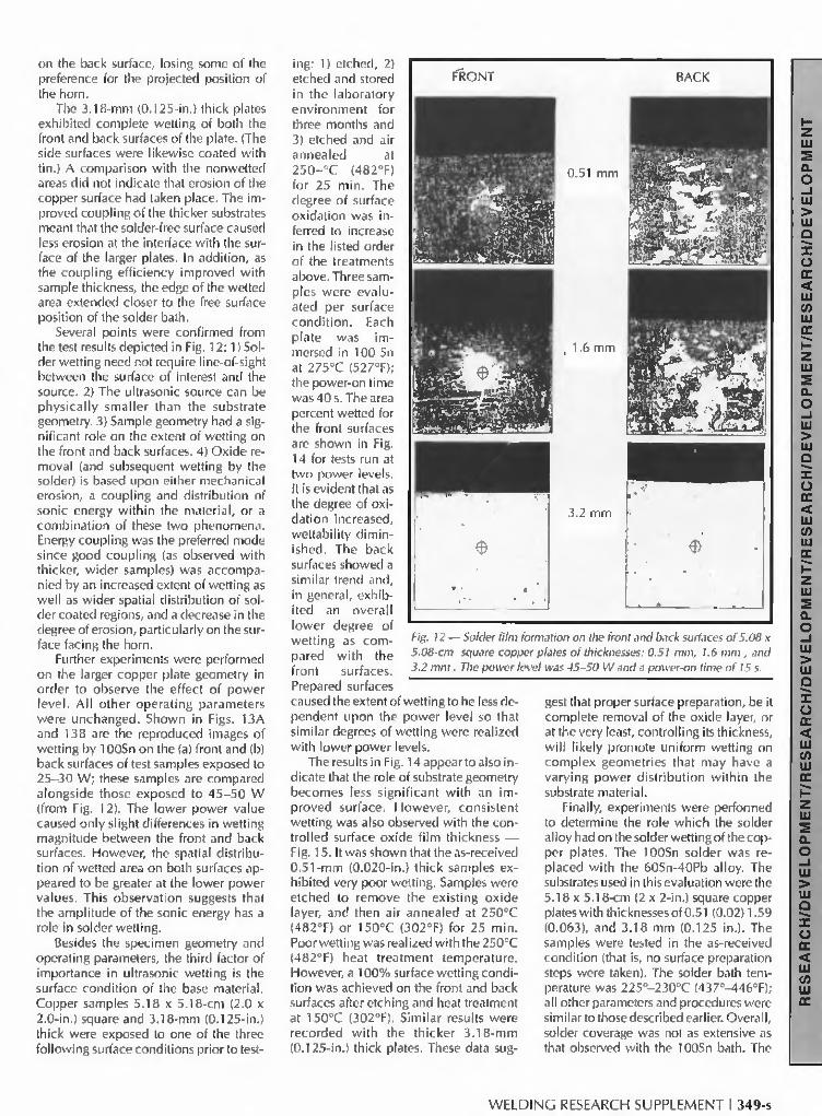
(2-in.) square copper plates having thick- nesses of 0.51 (0.02), 1.60 (0.063), and 3.18 mm (0.125 in.). The specimens were tested in the as-received condition. The horn-to-plate separation was 3.18 mm (0.125 in.). The power level was held at 45-50 W for a period of 15 s. The 0.51- mm (0.02-in.) thick plate was preheated by immersion in the bath (at zero power) for 1 min; the thicker 1.60- (0.063) and 3.18-mm. (0.125-in.) plates were pre- heated for 2 min. Shown in Fig. 12 are re- produced images of the solder film forma- tion on the front and back surfaces of the specimen plates. The cross-hair patterns indicated the projected position of the horn with respect to the sample (front) sur- faces. A solder coating was formed on both the front and back surfaces of each of the samples. The 0.51-mm (0.02-in.)-thick samples exhibited a small wetted area on the front surface that was centered about the projected location of the horn. The re° gions of solder wetting were accompanied by a significant amount of erosion. The back surface of the plates showed limited solder wetting; however, the wetted areas had a larger spatial distribution about the horn's projected position than was ob- served on the front surface. Wetting of the back surface confirmed the results from the smaller coupons; that is, the sonic en- ergy had coupled into the copper plate and was subsequently dispersed to the back surface.
The spatial extent and magnitude of wetting increased slightly with the 1.60- mm (0.063-in.) thick copper plate. Al- though the solder coating on the front sur- face remained localized to the line-of-sight position with the horn, some coating was observed along the outer edges. Wetting was further delocalized
3 4 8 - s I NOVEMBER 1996
on the back surface, losing some of the preference for the projected position of the horn.
The 3.18-mm (0.125-in.) thick plates exhibited complete wetting of both the front and back surfaces of the plate. (The side surfaces were likewise coated with tin.) A comparison with the nonwetted areas did not indicate that erosion of the copper surface had taken place. The im- proved coupling of the thicker substrates meant that the solder-free surface caused less erosion at the interface with the sur- face of the larger plates. In addition, as the coupling efficiency improved with sample thickness, the edge of the wetted area extended closer to the free surface position of the solder bath.
Several points were confirmed from the test results depicted in Fig. 12: 1) Sol- der wetting need not require line-of-sight between the surface of interest and the source. 2) The ultrasonic source can be physically smaller than the substrate geometry. 3) Sample geometry had a sig- nificant role on the extent of wetting on the front and back surfaces. 4) Oxide re- moval (and subsequent wetting by the solder) is based upon either mechanical erosion, a coupling and distribution of sonic energy within the material, or a combination of these two phenomena. Energy coupling was the preferred mode since good coupling (as observed with thicker, wider samples) was accompa- nied by an increased extent of wetting as well as wider spatial distribution of sol- der coated regions, and a decrease in the degree of erosion, particularly on the sur- face facing the horn.
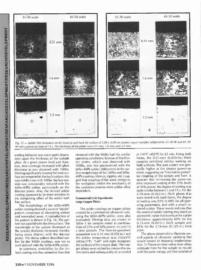
Further experiments were performed on the larger copper plate geometry in order to observe the effect of power level. All other operating parameters were unchanged. Shown in Figs. 13A and 13B are the reproduced images of wetting by 100Sn on the (a) front and (b) back surfaces of test samples exposed to 25-30 W; these samples are compared alongside those exposed to 45-50 W (from Fig. 12). The lower power value caused only slight differences in wetting magnitude between the front and back surfaces. However, the spatial distribu- tion of wetted area on both surfaces ap- peared to be greater at the lower power values. This observation suggests that the amplitude of the sonic energy has a role in solder wetting.
Besides the specimen geometry and operating parameters, the third factor of importance in ultrasonic wetting is the surface condition of the base material. Copper samples 5.18 x 5.18-cm (2.0 x 2.0-in.) square and 3.18-mm (0.125-in.) thick were exposed to one of the three following surface conditions prior to test-
ing: 1) etched, 2) etched and stored in the laboratory environment for three months and 3) etched and air annealed at 250-°C (482°F) for 25 min. The degree of surface oxidation was in- ferred to increase in the listed order of the treatments above. Three sam- ples were evalu- ated per surface condition. Each plate was im- mersed in 100 Sn at 275°C (527°F); the power-on time was 40 s. The area percent wetted for the front surfaces are shown in Fig. 14 for tests run at two power levels. It is evident that as the degree of oxi- dation increased, wettability dimin- ished. The back surfaces showed a similar trend and, in general, exhib- ited an overall lower degree of wetting as com- pared with the front surfaces.
0.51 mm
BACK
1.6 mm
3.2 mm
e
Fig. 12 - - Solder f i lm formation on the front and back surfaces o f 5.08 x
5.08-cm square copper plates o f thicknesses: 0.51 ram, 1.6 mm , and
3.2 mm . The power level was 45 -50 W a n d a power-on t ime o f 15 s.
Prepared surfaces caused the extent of wetting to be less de- pendent upon the power level so that similar degrees of wetting were realized with lower power levels.
The results in Fig. 14 appear to also in- dicate that the role of substrate geometry becomes less significant with an im- proved surface. However, consistent wetting was also observed with the con- trolled surface oxide film thickness - - Fig. 15. It was shown that the as-received 0.51-mm (0.020-in.) thick samples ex- hibited very poor wetting. Samples were etched to remove the existing oxide layer, and then air annealed at 250°C (482°F) or 150°C (302°F) for 25 min. Poor wetting was realized with the 250°C (482°F) heat treatment temperature. However, a 100% surface wetting condi- tion was achieved on the front and back surfaces after etching and heat treatment at 150°C (302°F). Similar results were recorded with the thicker 3.18-mm (0.125-in.) thick plates. These data sug-
gest that proper surface preparation, be it complete removal of the oxide layer, or at the very least, controlling its thickness, will likely promote uniform wetting on complex geometries that may have a varying power distribution within the substrate material.
Finally, experiments were performed to determine the role which the solder alloy had on the solder wetting of the cop- per plates. The 100Sn solder was re- placed with the 60Sn-40Pb alloy. The substrates used in this evaluation were the 5.18 x 5.18-cm (2 x 2-in.) square copper plates with thicknesses of 0.51 (0.02) 1.59 (0.063), and 3.18 mm (0.125 in.). The samples were tested in the as-received condition (that is, no surface preparation steps were taken). The solder bath tem- perature was 225°-230°C (437°-446°F); all other parameters and procedures were similar to those described earlier. Overall, solder coverage was not as extensive as that observed with the 100Sn bath. The
WELDING RESEARCH SUPPLEMENT I 349-s
~25--30 watts
0~gl mm
1.6 mm
3.2 mm
A
45-50 watts
• :! ' 4 . "
25-30 watts
0.51 mm
1.6 mm
3 . 2 m m
• • , . •
• . . , . . .
B
45-50 watts
Fig. 13 - - Solder film formation on the front (a) and back (b) surface of 5.08 x 5.08-cm square copper samples subjected to 25-30 W and 45-50
W and a power-on time o f 15 s. The thickness o f the plates was 0.51 mm, 1.6 mm, and 3.2 ram.
wetting behavior was once again depen- dent upon the thickness of the sample plate. At a given power level and dura- tion, area coverage increased with plate thickness as was observed with 100Sn. Wetting significantly favored the front sur- face as compared to the back surface; this was not the case with 100Sn. Surface ero- sion was considerably reduced with the 60Sn-40Pb solder, particularly on the thinnest plates. Also, the tin-lead solder coating appeared to be more sensitive to the dampening effect of the solder bath free surface.
The morphology of the 60Sn-40Pb solder coating showed a wave or "ripple" pattern comprised of alternating wetted and nonwetted areas. A reproduction of the pattern is shown in Fig. 16. The pat- tern ran parallel with the free surface. The wavelength of the pattern decreased as the sample thickness increased, thereby being more distinct with the thinner plates. The donut pattern described ear- lier for the 100Sn coatings, was not as well defined with the 60Sn-40Pb solder.
In summary, wettability by the tin- lead coating was less extensive than that
observed with the 100Sn bath for similar operating conditions. Erosion of the thin- ner plates, which was observed with 100Sn, was less pronounced with the 60Sn-40Pb solder• Differences in the sur- face morphology of the 100Sn and 60Sn- 40Pb coatings (donuts, ripples, etc.) sug- gest that coupling of the sonic energy to the workpiece and/or the mechanics of the cavitation process were solder alloy dependent.
Commercial Unit Experiments Large Copper Plates
The solder coatings on copper plates created by a commercial ultrasonic unit, using the 60Sn-40Pb solder, were also evaluated. Wetting data are shown in Table 1 for samples tested at combina- tions of 25% and 50% power, 5-s and 15 s time periods. The horn-to-specimen separation was 6.35 mm (0.250 in.) and the solder temperature was 250+5°C (482+10°F). "Left" and right designate the surfaces of the copper plate. The cop- per plates were etched to remove the na- tive oxide and subsequently air annealed
at 250°C (482°F) for 25 min. Using both horns, the 0.51-mm (0.020-in.) thick samples exhibited similar wetting on both surfaces. The data scatter was gen- erally higher at the shorter power-on times, suggesting an "incubation period" for coupling of the sample and horn. it appears that increasing the power-on time improved wetting at the 25% level; at 50% power, the degree of wetting was quite similar between 5 and 15 s. For the 3.18-mm (0.063-in.) thick plates that were tested with both horns, the degree of wetting was 83% to 88% for all oper- ating parameters, and with a much re- duced scatter. These trends indicate that the extent of solder coating may reach an asymptotic value that is unique for a plate thickness: approximately 60% for the 0.51-mm (0.02-in.) thick sample and 85% for the 3.18-mm (0.125-in.) thick plate.
The above observations illustrate sev- eral aspects of ultrasonic soldering that would impact its industrial implementa- tion. 1) Power-on time value must allow adequate time for the sample to couple with the sonic energy, yet limit erosion of
350-s I NOVEMBER 1996

100
80
Solder Coating 60 i
F r o n t
(%) 40 -
20
O .............
Etched
",,". \ / \ ,
" \ \
\ , " 0 ,5-60W \, 40 sec
\,\ , \
25-30W " " 40 sec \ % \ .
'\ \ 'k,
\ x. \ ' ,
', O 1 . . . . . •
Etched Etched & &
Stored Annealed
i
Fig. 14 - - The percentage o f the front surface wetted as a function of etched surface condit ion. The operating parameters were 100Sn (275°0 and a power-on time o f 40 s; the power levels accompany each o f the traces.
100 ~ -
Solder Coating
F r o n t
(%)
80
60
4 0 r
20
0
/ ,/
,.,/
55-60W // 40 sec / /
// ' / ' , /
// ,,/ // 25-30W
/ / 40 sec ,'/
, /
/{
Anneal Anneal 250C 150C
25 min 25 min
",I A w
As- Rec'd
Fig. 15 - - The percentage of the front surface wetted as a function of surface condition. The operating parameters were 100Sn (275°0 and a power-on time of 40 s; the power levels accompany each of the traces.
the substrate. 2) Solder coverage retains the strong substrate geometry depen- dence as was observed with the point source. 3) Assuming that adequate solder coverage is achieved for a given piece of hardware, then the insensitivity of wet- ting to slight process variations suggests a wide manufacturing window for that application.
Test samples were also evaluated with one horn operating at power/power-on times of either (25%, 5 s) or (50%, 15 s). At 25% power for 5 s, the degree of wet- ting was equivalent on both surfaces of the plate in all cases. The magnitude of wetted surface was slightly higher with one horn than when both horns were op- erating under the same parameters; al- beit, the significance of this trend was limited by the data scatter. Increasing the power and power-on time to 50 W and 15 s, respectively, caused the side ex- posed to the horn to achieve a coverage equivalent to that when both horns were operating. However, wetting of the back surface remained low. These observa- tions suggest that the use of two ultra- sonic sources against a single specimen may give somewhat unpredictable re- sults likely caused by interference be- tween the energy waves that couple into the sample.
In the case of the 3.18-mm (0.125-in.) thick samples, the use of a single horn re- duced the extent of wetting and pro- duced a significant increase in the data scatter. Also, both surfaces of the sample
exhibited similar degrees of wetting. In summary, experiments with the
commercial unit provided benchmark results as to the wetting performance of single copper plates. The increased amount of power made available with the commercial unit posed some unique concerns. Under the use of two horns, the extent of wetting appeared to reach a maximum value that was determined by the substrate thickness. The maximum percent coverage decreased as the plate thickness diminished. It was also observed that for thin- ner sections, one ultrasonic source can provide better wetting as compared with two sources, suggesting pos- sible interference phenom- ena. The thicker specimens (3.81 mm) were not sensitive to this artifact; rather, the re- duced overall energy input into the substrate with the use of a single horn, simply reduced the maximum wet- ting area. The wetted area remained more-orqess equivalent for both surfaces.
It was of interest to ex- tend the use of ultrasonic soldering to the formation of solder joints. X-ray radiogra- phy was used to image sol- der fill, in the gap between two copper plates - - Fig. 3. The solder was 60Sn-40Pb
at 250°C and the horn-to-sample separa- tion, 6.35 mm (0.250 in.). Two 1.59-mm (0.063-in.) thick copper plates were as- sembled with a 0.25-mm (0.010-in.) joint clearance between them. Joint clear- ances of 0.076 mm (0.003 in.) and 0.127 mm (0.005 in.) were also evaluated (same plate thickness). It was verified that solder did not fil l the joint clearance upon immersion. Microanalysis of the clearance cross section revealed the for- mation of an i ntermetallic layer at the sol-
Fig. 16 - - Reproduction of the 60Sn-40Pb solder coating on a 5.08 x 5.08 x 0.051-cm copperplate. The solder bath was at 228°C with 0.635-cm horn-to-sample separation. The power level was 55-60 W and held for 15 s.
WELDING RESEARCH SUPPLEMENT I 351-s

Capillary Rise
H
(cm)
5.00
4.00
3.00
2.00
1.00
0
-1.00 i"
t 0
' 0 I J I
Flux
F " . . . . . . . . . . . . . . . . . . . . . . . . . . . . .
e / e ~ o older
0.010 0.020 0.030 Gap (cm)
Fig. 17 - - Effective capillary rise as a function of gap width for 1.59-mm-thick copper samples exposed to 50% power for 15 s in 605n-40Pb solder at 250°C.
/ . , /P la tes
Solder Bath Surface
; : ; : i . . , . .
: "" " "~ ' : .'.: ~" Region " . . . • . .
3 i ;3 ; : o, ~ Contact ; : : - !
• . '" :-.i? :. ' . : ' . '" • . . . . ,
(a)
j ~ P l a t e s
Solder Bath Surface
• ;•!;i;
iii.!!.:. ".: :': '.'. i" .: :- '. ". • . . . . - - ' . . .
. . . • . , . ° °
- ° o .
• ". :-..'.'.-:;::.'.':.'-
(b)
Fig. 18 - - Schematic diagram showing the solder capillary geometry for f i l l ing the parallel plate
jo int clearance.
der/substrate interface, thereby verifying that wetting had taken place (as opposed to simply the presence of frozen solder in the joint clearance).
Shown in Fig. 17 are data represent- ing the effective capillary rise of the sol- der as a function of clearance thickness. The power was 50% and the time dura- tion, 15 s. Baseline data were also ob- tained for samples immersed into the sol- der, using a rosin-based, mildly activated flux, but without ultrasonic activation• Under ultrasonic activation, it was noted that except for the smallest joint clear- ance of 0.076 mm (0.003 in.), the solder filled to approximately the level of the bath, but no further. The magnitude of the meniscus height depended upon joint clearance thickness and was consider-
ably less in the ultrasonic case as com- pared with behavior in the presence of a flux over the same clearance range.
A hypothesis was developed to ex- plain the limited capillary rise by the sol- der - - Fig. 18. Previous studies showed that the oxide removal process required solder to be in contact with the substrate surface. Under the hydrostatic head cre- ated by the sample immersion, a convex shape was created by the liquid profile which caused it to contact a small area of the plate surfaces at the base of the clear- ance. Cavitation was able to remove the oxide film, and thus, allow the solder to both wet and "protrude" further up the surface. This process continued as the solder filled the joint clearance. How- ever, when the solder had risen to the
level of the bath, the hydrostatic head was lost, as was the small line of contact ahead of the wetted surface created by the solder surface curvature• Further wet- ting could not take place.
The capillary rise was very limited with the smallest clearance, 0.076 mm (0.003 in.). At the smaller joint clearance, the surface tension of the solder did not permit the molten metal to reach within the plates so as to effect the cavitation process. Therefore, it appears that a min- imum clearance exists that wil l permit the solder profile to partially contact the surfaces. (An alternative is the placement of a solder preform into the joint clear- ance and allowing it to melt prior to ul- trasonic activation)•
Finally, it was noted that there was an absence of voids in the solder that filled the joint clearance by ultrasonic activa- tion. This attribute presents a clear ad- vantage over the traditional use of fluxes that typically generates voids in joint clearance or confined geometries.
Summary - - Fundamental Studies
Experiments using the point source ul- trasonic horn, 100Sn, and copper plates as well as the commercial unit with 60Sn-40Pb demonstrated that oxide re- moval through solder cavitation resulted from a combination of mechanical ero- sion and the coupling of ultrasonic en- ergy to the substrate geometry• The en- ergy was dispersed within the substrate body so that the cavitation process could potentially operate on surfaces of the substrate that were not in line of sight of the source (horn). Because the cavitation process can only take place where the solder contacts the sample surface, the rise of a solder film above the surface of the reservoir (whether in a joint clear- ance or on an open plate geometry) is not possible by this technique. Erosion processes dominated when poor cou- pling occurred between the sonic energy and the substrate.
The substrate materials, substrate geometry, and source-to-substrate con- figuration were important factors in ul- trasonic wetting• In general, thicker sec- tions (with respect to the line of sight of the source) exhibited better wetting (the result of good coupling and minimum erosion), particularly at lower power lev- els and reduced time periods• The degree of wetting was also dependent upon the particular solder alloy as well as the op- erating parameters of the horn(s).
The extension of ultrasonic soldering to the fabrication of actual joints was ex- amined by the wetting of molten metal within a gap formed between two paral-
352-s I NOVEMBER 1996
lel copper plates. Owing to the require- ment that solder must contact the surface in order to support the oxide removal process (cavitation), capillary rise above the reservoir surface was not achieved. Also, immersion of the substrate into the solder bath would be a requirement for ultrasonic soldering to produce a joint.
Ultrasonic activation would be a vi- able technique for numerous industrial soldering applications. Nondestructive techniques such as x-ray radiograph or sonic imaging would be suitable tools for joint inspection. Studies which illustrate the use of ultrasonic soldering for the sol- der coating of circuit board features and device package leads will comprise the applications.
A p p l i c a t i o n s
Printed Circuit Board Solder Coating
Miniature Circuit Board Test Vehicles
Precoating metal surfaces with a thin solder layer preserves solderability dur- ing long-term storage, prior to actual as- sembly. In the case of electronic circuit boards, application of the solder precoat has been done by the hot air solder lev- eling (HASL) procedure. By this tech- nique, the circuit board is coated with flux and then immersed into a solder bath. Upon removal from the molten sol- der, the board is transported past a pair of hot air knives which remove excess sol- der prior to solidification, leaving a thin coating on the conductor features (Ref. 13). The adaptation of ultrasonics to the HASL process was developed by earlier investigators. However, very little data is available which describes the response
of printed circuit boards to ultrasonic activation (Ref. 8).
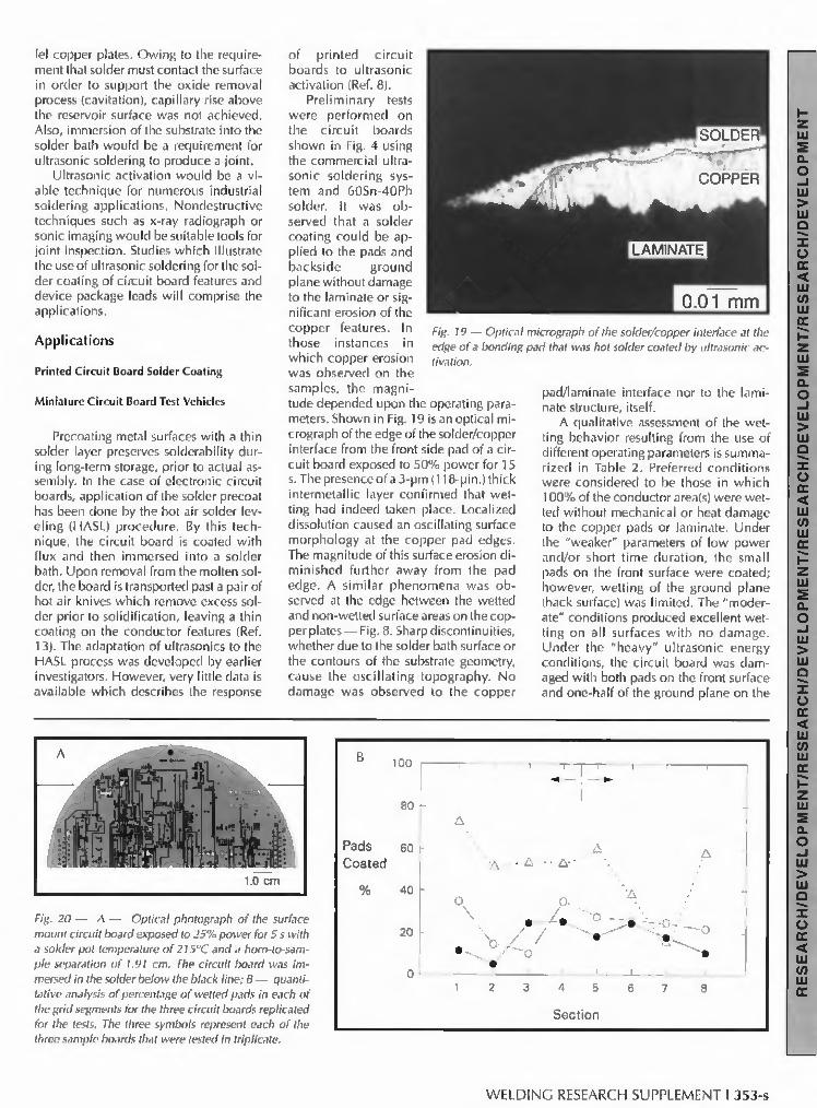
Preliminary tests were performed on the circuit boards shown in Fig. 4 using the commercial ultra- sonic soldering sys- tem and 60Sn-40Pb solder. It was ob- served that a solder coating could be ap- plied to the pads and backside ground plane without damage to the laminate or sig- nificant erosion of the copper features. In those instances in which copper erosion was observed on the samples, the magni- tude depended upon the operating para- meters. Shown in Fig. 19 is an optical mi- crograph of the edge of the solder/copper interface from the front side pad of a cir- cuit board exposed to 50% power for 15 s. The presence of a 3-pm (118-lain.) thick intermetallic layer confirmed that wet- ting had indeed taken place. Localized dissolution caused an oscillating surface morphology at the copper pad edges. The magnitude of this surface erosion di- minished further away from the pad edge. A similar phenomena was ob- served at the edge between the wetted and non-wetted surface areas on the cop- per plates-- Fig. 8. Sharp discontinuities, whether due to the solder bath surface or the contours of the substrate geometry, cause the oscillating topography. No damage was observed to the copper
Fig. 19 - - Optical micrograph of tire solder/copper interface at tire edge of a bonding pad that was hot solder coated by ultrasonic ac- tivation.
pad/laminate interface nor to the lami- nate structure, itself.
A qualitative assessment of the wet- ting behavior resulting from the use of different operating parameters is summa- rized in Table 2. Preferred conditions were considered to be those in which 100% of the conductor area(s) were wet- ted without mechanical or heat damage to the copper pads or laminate. Under the "weaker" parameters of low power and/or short time duration, the small pads on the front surface were coated; however, wetting of the ground plane (back surface) was limited. The "moder- ate" conditions produced excellent wet- ting on all surfaces with no damage. Under the "heavy" ultrasonic energy conditions, the circuit board was dam- aged with both pads on the front surface and one-half of the ground plane on the
A •
;' I J " .
1 0 cm
Fig. 20 - - A - - Optical photograph of the surface mount circuit board exposed to 25% power for 5 s with a solder pot temperature of 215°C and a horn-to-sam- ple separation of 1.91 cm. The circuit board was im- mersed in the solder below the black line; B - - quanti- tative analysis of percentage of wetted pads in each of the grid segments for the three circuit boards replicated for the tests. The three symbols represent each of the three sample boards that were tested in triplicate.
Pads Coated
%
10o
80 ,- I i
60 ~
40
2 0 I
0 '
A
, .A. A • ::,~ . . . . :~ -- A'-
• / ~ , '
© 0, • .
• ......... °/-/--c / • ~ ' ~ - o • : i i i
1 2 3 4 5 6 7 8
Section
]
i I
i
q
WELDING RESEARCH SUPPLEMENT I 353-s
Pads Coated
%
I 1oo I-
I
80 1 ~ i
60
,o r 20 -
1
7 ,
2 3 4 5 6 7 8 Section
~. 260C, 75%, 30 sec, 0.6 cm | 0 215C. 75%. 5 sec. 1.9 crn I • 215C, 25%, 5 $ec, 1.9 cm
Fig. 21 - - Pad wetting on the surface mount circuit boards for the three test conditions shown in the insert. Each data point represents the mean of three duplicate test sam oles and an error of plus-or-minus one standard deviation.
served under long-term ex- posure to the higher pot tem- peratures. The quantitative analysis began with the circuit board exposed to 25% power for 5 s in a sol- der tempera- ture of 215°C (419°F). The horn-to-sample separation was 1.91 cm (0.750 in.). A photo- graph of a tested circuit board (25% power, 5 s, 215°C (419°F) solder temper- ature, 1.91 cm (0.750 in.)
back surface being completely eroded from the laminate. The operating para- meters used in these trials provided a suitable process window with which to more fully investigate the solder coating of printed circuit boards.
Large Surface Mount Circuit Board Test Vehicle
Next, experiments were performed on the single-sided, surface mount printed circuit board shown in Fig. 5. Qualitative observations confirmed that no damage had taken place to the laminate structure as a result of the test parameters. Some discoloration of the solder mask was ob-
horn/sample separation) is
shown in Fig. 20A. The test vehicle was immersed to below the black line. The percentage values of wetted lands within each of the grid segments from the three test vehicle replicates (each of which is represented by one of the symbols) are shown in Fig. 20B. The combined per- centage of wetted pads for the entire im- mersed surface was 18+8%. There was no apparent trend in the degree of wet- ting as a function of position on the board (i.e., center regions vs. those towards the edges).
Although wetting varied between the three test specimens, each of the three boards maintained the same wettability
level relative to one another. For exam- ple, the particular board represented by the open triangles tended to have greater wetting than the other samples. These observations suggest that either the sur- face oxide thickness between the boards was slightly variable, or that each board may have coupled differently into the sonic energy from the horn. Dissimilar coupling may have been caused by slight variations in the manner in which the board was held or small differences in board position relative to the horn.
Increasing the sonic energy input to the circuit board (through either more power, increased immersion time, or shorter distance between the board and the horn) as well as the use of higher pot temperatures reduced the variability of wetting, both on a given board surface as well as between similarly exposed test samples. The graph in Fig. 21 shows the percentage of pads wetted for each of the eight segments of a board. The three data sets represent different degrees of ultra- sonic energy in descending order of severity: 260 °C (500°F), 75%, 30 s, 0.64 cm (0.250 in.)), 215°C (419%), 75%, 5 5, 1.91 cm (0.750 in.), and 215°C (419%), 25%, 5 s, 1.91 cm (0.750 in.). Each data point represents the mean of three sam- ples; the error bar is one standard devia- tion. As expected, increased sonic energy improved the extent of solder wetting at a given pot temperature, power-on time, and horn/specimen separation. A nearly 100% coverage at the 260°C (500°F) sol- der temperature and reduced horn sepa- ration was accompanied by a significant decrease in variability (note the error bars). Damage to the laminate or copper features was not observed under any of the test conditions. Also, wetting near the board edges was similar to the interior so
g
g ¢J
20 ::
1 6 ; :
?
1 2 ~-: 2
[ ,
i l , '- - ~ t i
0 4 5 0 9 0 0 1 3 5 0 1800
Distance (urn)
20 ::
: i
16 ::
~ 12!
8 i : i
; !1 i
0 - 0 4 5 0 9 0 0 1 3 5 0 1800
Distance (~m)
Fig. 22 - - Electron microprobe traces along the solder coating on Au-plated leads. A - - Profile after coating with an RMA flux and immersion in the solder pot without ultrasonic activation; B - - that of the sample exposed to 50% power for 5 s without a flux. The origin of the trace is the lead-
ing edge of the film.
354-s I NOVEMBER 1996
that the lateral dimensions of the board (beyond the projected posit ion of the horn) were of no consequence to solder coverage.
Hot Solder Coating of Device Package Leads
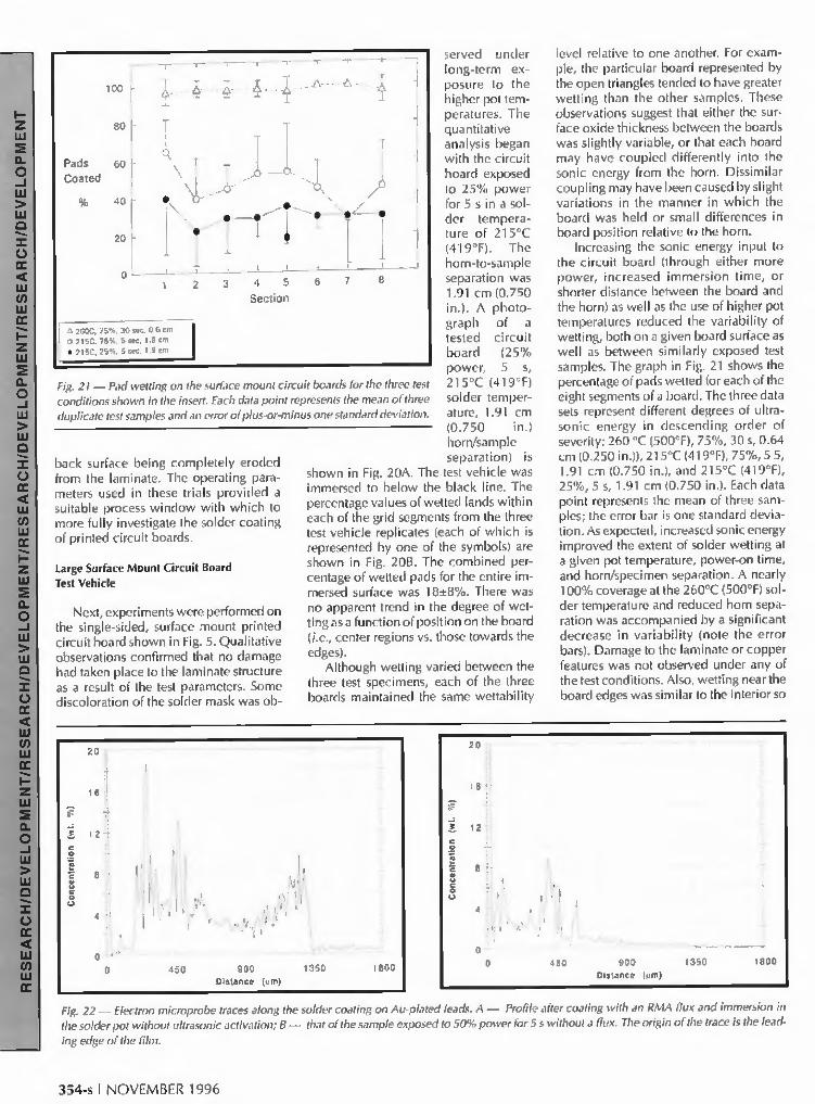
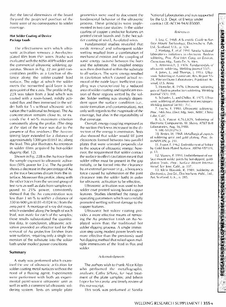
The effectiveness with which ultra- sonic activation removes a Au-electro- plated film fiom thin wires (leads) was evaluated with the 60Sn-40Pb solder and the commercial ultrasonic soldering ap- paratus. Shown in Fig. 22 are gold con- centration profiles as a function of dis- tance along the solder-coated lead surface. The edge at which the solder meets the nonwetted gold layer is the zero point of the x axis. The profile in Fig. 22A was taken from a lead which was coated with a rosin-based, mildly acti- vated flux and then immersed in the sol- der bath for 5 s without ultrasonic acti- vation (the traditional technique). The Au concentration remains close to, or ex- ceeds the 4 wt-% maximum criterion consistently along the profile. (The drop at the start of the trace was due to the presence of flux resiclues.) The Au-con- taining layer extended for a distance of approximately 1300 IJm (0.051 in.) along the lead. This plot illustrates Au retention in solder films acquired by hot-solder dipping (Ref. 12).
Shown in Fig. 22B is the Au trace from the sample exposed to ultrasonic activa- tion (50% power for 5 s). The Au profile shows a decrease in the percentage of Au as the trace becomes distant from the in- terface. Moreover this profile, along with the other traces from the second group of test runs as well as data from samples ex- posed to 25% power, consistently showed that the Au concentration was less than 1 wt-% to within a distance of 350 to 600 t_Jm (0.01-0.024 in.) from the zero point. A montage of x-ray clot maps, which extended along the length of each lead, was made for each of the samples; these results substantiated the quantita- tive data. In conclusion, ultrasonic acti- vation provided an effective tool for the removal of Au protective finishes from wire surfaces, requiring only a single im- mersion of the substrate into the solder bath under modest power conditions.
Summary
A study was performed which exam- ined the use of ultrasonic activation for solder coating metal surfaces without the need of a f luxing agent. Experiments were performed wi th both an experi- mental point-source ultrasonic unit as well as with a commercial ultrasonic sol- dering system. Tests on simple plate
geometries were used to document the fundamental behavior of the ultrasonic process. These principles were imple- mented in two case studies: 1 ) the solder coating of copper conductor features on printed circuit boards and 2) the hot sol- der coating of small, Au-plated wires.
Fundamental studies revealed that oxide removal and subsequent solder wetting resulted from a combination of mechanical erosion and the coupling of sonic energy (waves) between the horn and the substrate. The coupled energy was then distributed within the substrate to all surfaces. The sonic energy resulted in cavitation which caused actual re- m()val of the oxide layer. Inefficient cou- pling was characterized by a reduced area of solder coating and significant ero- sion of those regions wetted by the sol- der. Solder wetting was strongly depen- dent upon the surface condi t ion (i.e., oxide formation and contamination), not only with regards to the magnitude of the coverage, but also in the repeatability of that coverage.
Overall, energy coupling improved as the section thickness increased in the di- rection of the energy transmission. Tests also showed that solder would fill joint clearances formed between two parallel plates that were oriented perpendicular to the source of ultrasonic energy; how- ever, the requirement that solder contact the surface to effect cavitation meant that solder either must be present in the gap initially, or be forced into the clearance by an external pressure (e.g., a buoyancy force caused by submersion of the joint clearance into the solder bath) in order for ultrasonic activation to be effective.
Ultrasonic activation was used to hot solder coat printed wir ing board copper features. Studies identified the range of operating parameters which successfully promoted wetting without damage to the copper features.
Ultrasonic hot solder coating pro- vides a more effective means of remov- ing the Au protective finish on Au-Ni- plated wires than the tradit ional hot solder dipping process. A single immer- sion step using modest power levels was more effective than the previously used hot dipping method that relied upon mul- tiple immersions of the lead in flux and solder.
Acknowledgments
The authors wish to thank Alice Kilgo who performed the metal lographic analyses; Cathy Sifford, for heat treat- ment of the plate samples; and Edwin Lopez for his careful and timely review of this manuscript.
This work was perforrned at Sandia
National Laboratories and was supported by the U.S. Dept. of Energy under contract DE-ACO4-94AL85000.
References
I. Lea, C. 1988. A Scientific Guide to Sur- face Mount Technology, Electrochem. Pub. Ltd., Scotland, U.K., p. 324.
2. Hosking, F., eta/. 1991. Sandia National laboratories initiatives in electronic fluxless soldering. Pro(. First Inter. Cong. on Environ. Conscious Mt~4., Santa Fe, N. Mex.
3. Antonevich, I. 1976. Fundamentals of ultrasonic soldering. Welding Journal 55(7).
4. Jones, I., and Thomas, I. 1955. Ultra- sonic Soldering of Aluminum, Res. Report 55- 24, Pitman-Dunn Laboratories, Frankford Ar- senal, U.S. Army.
5. Humcke, R. 1976. Ultrasonic soldering pots of fluxless production soldering. Welding Journal 55(3): 191.
6. Schuster, J., and Chilko, R. t975. Ultra- sonic soldering of aluminunl heat exchangers. Welding Journal 54(10): 711.
7. Fuchs, F. 1990. Ultrasonic soldering. Proc. 14th Ann. Elect. Mti~. Sere., NWC, China Lake, Calif.
8. U.S. Patent 4,763,829, Soldering of Electronic Components. W. Sherry, AT&T Bell Laboratories, Aug. 16,1988.
9. MIL-STD1276D. 10. Bester, M. 1968. Metallurgical aspects
of soldering gold and gold plating. Pro(. In- terNEPCON, p. 211.
11. Foster, F. 1962. Embrittlement of Solder by Gold from Plated Surface. ASTM-STP319, p. 13.
12. Vianco, P. 1993. Embrittlement of sur- face mount solder joints by hot-dipped, gold- plated leads. Proc. Surface Mount Interna- tional, San Jose, Calif., p. 337.
13. Klein Wassink, R. 1989. Soldering in Electronics, 2nd Ed., Electrochem. Publ., Ltd., Ayr, Scotland, U.K., p. 285.
W E L D I N G RESEARCH SUPPLEMENT I 355-s