Ultrasim Workshop 11.1
153
UltraSim Workshop Version 11.1 August. 2011 MMSIM11.1 IC6.1.5 ISR5 IUS 10.2
description
Useful workshop on EM/IR
Transcript of Ultrasim Workshop 11.1

UltraSim Workshop
Version 11.1
August. 2011
MMSIM11.1 IC6.1.5 ISR5
IUS 10.2

UltraSim Workshop
Feb 2010 1
2006-2011 Cadence Design Systems, Inc. All rights reserved worldwide. Printed in the United States of America. Cadence Design Systems, Inc., 555 River Oaks Parkway, San Jose, CA 95134, USA Trademarks: Trademarks and service marks of Cadence Design Systems, Inc. (Cadence) contained in this document are attributed to Cadence with the appropriate symbol. For queries regarding Cadence’s trademarks, contact the corporate legal department at the address shown above or call 1-800-862-4522. All other trademarks are the property of their respective holders. Restricted Print Permission: This publication is protected by copyright and any unauthorized use of this publication may violate copyright, trademark, and other laws. Except as specified in this permission statement, this publication may not be copied, reproduced, modified, published, uploaded, posted, transmitted, or distributed in any way, without prior written permission from Cadence. This statement grants you permission to print one (1) hard copy of this publication subject to the following conditions: 1. The publication may be used solely for personal, informational, and noncommercial purposes; 2. The publication may not be modified in any way; 3. Any copy of the publication or portion thereof must include all original copyright, trademark, and other proprietary notices and this permission statement; and 4. Cadence reserves the right to revoke this authorization at any time, and any such use shall be discontinued immediately upon written notice from Cadence. Disclaimer: Information in this publication is subject to change without notice and does not represent a commitment on the part of Cadence. The information contained herein is the proprietary and confidential information of Cadence or its licensors, and is supplied subject to, and may be used only by Cadence’s customer in accordance with, a written agreement between Cadence and its customer. Except as may be explicitly set forth in such agreement, Cadence does not make, and expressly disclaims, any representations or warranties as to the completeness, accuracy or usefulness of the information contained in this document. Cadence does not warrant that use of such information will not infringe any third party rights, nor does Cadence assume any liability for damages or costs of any kind that may result from use of such information. Restricted Rights: Use, duplication, or disclosure by the Government is subject to restrictions as set forth in FAR52.227-14 and DFAR252.227-7013 et seq. or its successor.

UltraSim Workshop
Feb 2010 2
Table of Contents 1. Using UltraSim in Analog Design Environment (ADE) I 5
1.1 Simulating a 8-bit-multiplier in ADE 5
2. Using UltraSim in Analog Design Environment II 16
2.1 Simulating the PLL using pre-layout netlist 16
2.2 Simulating the PLL with VerilogA VCO model 27
2.3 Simulating the PLL using post-layout netlist 31
3 Using Digital Vector Files 35
3.1 Simulating a 16-bit multiplier with digital vector file 35
3.2 Using VCD/EVCD Files 39
3.3 Simulating a small case with VCD file 39
3.4 Simulating the same case with EVCD file 43
4 Using Structural Verilog Netlists 46
4.1 Simulating a multiplier with structural Verilog netlist 46
5 Hierarchical versus Flat Mode Simulation 49
5.1 Running flat mode simulation on a 16Kb SRAM 49
5.2 Running hierarchical simulation on the 16K SRAM 51
5.3 Other UltraSim options 52
6 Post-Layout Simulation with RC Back Annotation 53
6.1 Simulating the pre-layout circuit 53
6.2 Simulating the post-layout netlist with DSPF parasitic RC file 55
6.3 Simulating the post-layout circuit with the SPEF parasitic RC file 58 6.4 Resistor and Capacitor Statistical Checks 61
7 UltraSim Power and Design Analyses 62
7.1 Simulating a high voltage charge pump 62
7.2 Probing voltage or current of an element or subcircuit 64
7.3 Probing power of a subcircuit 65
7.4 Using Dynamic Power Analysis to calculate the efficiency of the pump 66 7.5 Power Analysis on a subcircuit 67
7.6 Node activity analysis 68
7.7 Node Glitch Analysis 69
7.8 Power Checking Analysis 72
7.9 Hot Spot Node Current Check 73
7.10 Design Checking Analysis (Device Voltage Check) 74
7.11 Active Node Checking Analysis 76
7.12 Netlist Parameter Check 77
7.13 Substrate Forward Bias Check 78
7.14 Static MOS Voltage Check 79
7.15 Static NMOS/PMOS BULK Forward Bias Check 80
7.16 Detect Always Conducting NMOS/PMOS 81
7.17 Static Diode Voltage Check 82
7.18 Post-processing measurement flow 82
7.19 Static RC Delay Check 84
8 UltraSim Power Solver 85
9 DC leakage analysis 94
10 Static ERC Checks 100
11 Timing Analysis 104
11.1 Simulating the 16K bit SRAM 104
11.2 Pulse Width Check 105
11.3 Setup Check 106
11.4 Hold Check 107
UltraSim Workshop
Feb 2010 3
12 Simulating Voltage Regulators (Voltage Regulator Option) 108
13 Multithreading Simulation 112
14 Static Power Grid Calculator 113
15 Electro-Migration and IR-Drop analysis 115
15.1 Running UltraSim Simulation 116
15.2 Post-Processing for EM and IR analysis 120
15.3 IR analysis 125
14.4 EM Analysis 132
16 Case Studies 142
16.1 Case Study: Using the UltraSim Save and Restart features 142
16.2 Case study: Bisection optimization 144
16.3 Case study: HCI & NBTI Reliability analysis 148
Cadence Education Services 152
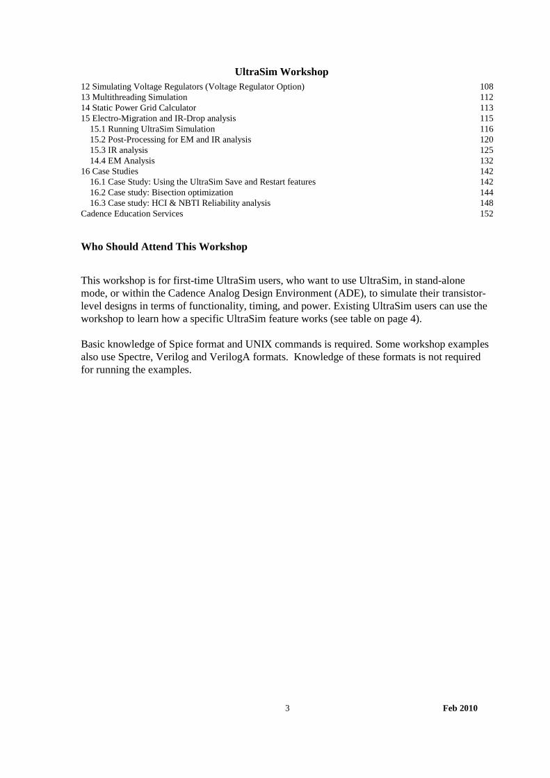
Who Should Attend This Workshop
This workshop is for first-time UltraSim users, who want to use UltraSim, in stand-alone mode, or within the Cadence Analog Design Environment (ADE), to simulate their transistor-level designs in terms of functionality, timing, and power. Existing UltraSim users can use the workshop to learn how a specific UltraSim feature works (see table on page 4). Basic knowledge of Spice format and UNIX commands is required. Some workshop examples also use Spectre, Verilog and VerilogA formats. Knowledge of these formats is not required for running the examples.

UltraSim Workshop
Feb 2010 4
Setup for the Workshop Examples Make sure you read the UltraSim Workshop Setup document and follow the setup instructions. The examples in this workshop were developed using MMSIM11.1, IC6.1.5 ISR5, and IUS10.2. Some of the features described in this workshop are not supported by earlier releases of the software tools. The UltraSim_Workshop directory contains the following sub-directories:
Sub-directories Circuit Type UltraSim Features Demonstrated
mult16_vec Digital circuit Hierarchical digital vector format support. Vector check waveform. Logic probe.
vcd_hier Digital circuit Hierarchical VCD/EVCD format support. mult16_vlog Digital circuit Structural Verilog netlist support.
Timing analysis. sram16k Memory circuit Hierarchical vs. flat mode simulation.
sram16k_ta Memory circuit Timing analysis. Vector check waveform.
dram1gb Memory circuit Ultra-large circuit simulation. Save and restart.
pump Analog circuit Current/power probe, Power analysis Power checking analysis, Design checking analysis, Node activity analysis, Substrate Forward Bias Check, Static MOS Voltage Check, Static NMOS Bulk Forward Bias Check, Static PMOS Bulk Forward Bias Check, Detect Always Conducting NMOSFETs, Detect Always Conducting PMOSFETs
dc_path Analog circuit DC leakage path checking Filter warning messages Partition and node connectivity analysis
DFF Digital circuit Bisection search osc13 Analog circuit Reliability analysis mult16_vr Analog circuit Voltage Regulator Option
Multithreading Simulation post_layout Memory circuit Post-layout simulation.
RC back annotation. DSPF & SPEF format support.
SPRES DSPF file Static Power Grid Calculator sp_mult RF circuit Envelope Following Transient Analysis ups Analog circuit Power net detection (2 methods)
Fast simulation with power net mult Digital circuit UltraSim interface in ADE
Spectre/Spice netlist support. pll Mixed signal circuit UltraSim interface in ADE.
VerilogA module support Post layout simulation.
EMIR – Electro- Migration and IR-drop analysismult
Digital circuit Postlayout analysis, back annotation and stitching Post processing for EM & IR-drop values Integration with physical layout environment Graphic and text based EM and IR-Drop reporting UltraSim interface in ADE Spectre/Spice netlist support.

UltraSim Workshop
Feb 2010 5
1. Using UltraSim in Analog Design Environment (ADE) I Ultrasim can work in standalone mode, in ADE or Composer. Ultrasim, as a fast spice simulator, supports both global and local options. The global options are applicable to the whole design while the local options are applicable to subckts, instances and models. In this lab we will study the basic setup in ADE to run Ultrasim, including transient analysis setup, global options setup, output and model library setup. More advanced features, like local option setup, will be covered in the next lab. Setup Environment In this lab, we will run simulation with UltraSim in either ADE or Composer. Before starting the lab, you need to make sure that the environment setup is correct. There is an example config file called “setup.csh” in the workshop directory. Please look at this file and verify these key variables’ value before you start to run the case:
$CDSHOME $IUSHOME $USIMHOME $FLOW
Note that this lab works with IC613.511 or later releases, otherwise you may not see some features. The variable $FLOW is for the next two labs as well as the EMIR lab. 1.1 Simulating a 8-bit-multiplier in ADE Action 1: Configure the environment variables and run ./CLEAN
%source setup.csh %./CLEAN
The Cadence analog design environment (ADE) provides the interface to the UltraSim simulator. This example demonstrates the UltraSim netlisting and simulation control in ADE.
Action 2: Change to the mult directory.
% cd modules/mult
Action 3: Start IC design framework.
% virtuoso & Action 4: If the Library Manager window has been opened, jump to the next step. Otherwise,
open the Library Manager window from the Command Interpreter Window (CIW).
[CIW] Tools ���� Library Manager…

UltraSim Workshop
Feb 2010 6
Action 5: In the Library Manager window,
� click toplib ` in the Library panel. � Then click MultWDAC ` in the Cell panel. � Finally double click schematic in the View window. This will open Virtuoso
Schematic Editing window for MultWDAC.
Action 6: Let us first exam the top multiplier cell. In the Virtuoso Schematic Editing window, click Edit ���� Hierarchy ���� Descend Edit. Click to select the top multiplier cell and open the schematic view. Following the same procedure, you can also push into one of the mul44_core cells. Note in IC614 or later releases, you can open the schematic in a new tab, current tab or new window. In this case, we will choose current tab.
After you are done, return to the top of the design hierarchy by Edit����Hierarchy����Return to Top
Action 7: Start the analog design environment.
[Virtuoso Schematic Editor] Launch ���� ADE L Note: IC6.x provides three environments: ADE L/XL/GXL. ADE L is the basic ADE and supports basic analysis. ADE GXL is the most powerful ADE and supports all the functions. For more information, please refer to the ADE User Guide.
Action 8: In the ADE window, change simulator to UltraSim (see Fig.1.1), and make sure you
see the words Simulator:UltraSim at the lower right corner of the ADE window.
[ADE] Setup ���� Simulator/Directory/Host…
Fig.1.1 Choose UltraSim simulator in ADE
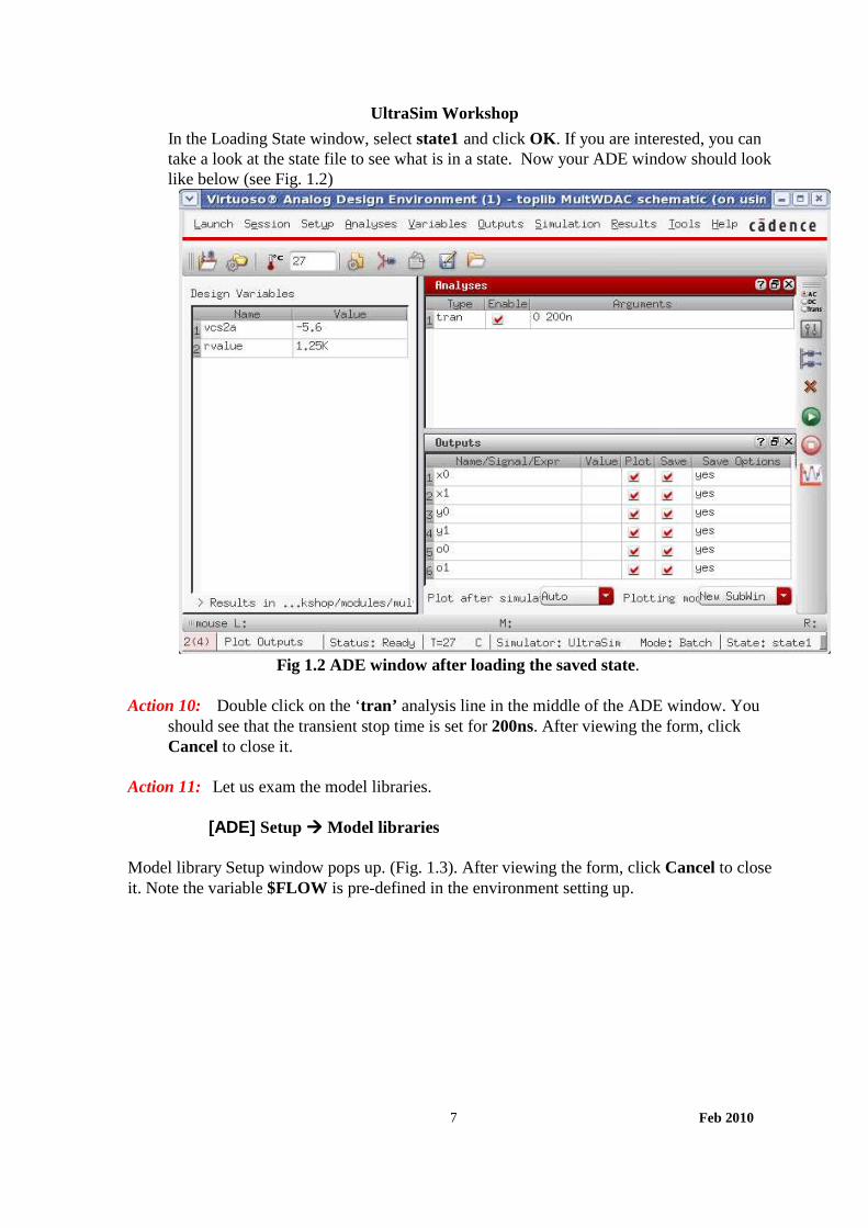
Action 9: Now load the simulation state.
[ADE] Session ���� Load State…
UltraSim Workshop
Feb 2010 7
In the Loading State window, select state1 and click OK . If you are interested, you can take a look at the state file to see what is in a state. Now your ADE window should look like below (see Fig. 1.2)
Fig 1.2 ADE window after loading the saved state.
Action 10: Double click on the ‘tran’ analysis line in the middle of the ADE window. You
should see that the transient stop time is set for 200ns. After viewing the form, click Cancel to close it.
Action 11: Let us exam the model libraries. [ADE] Setup ���� Model libraries Model library Setup window pops up. (Fig. 1.3). After viewing the form, click Cancel to close it. Note the variable $FLOW is pre-defined in the environment setting up.

UltraSim Workshop
Feb 2010 8
Fig. 1.3. Model libraries setup window
Action 12: Look at some of the UltraSim options (Fig. 1.4)
[ADE] Simulation ���� Options ���� Analog …
These are the global options of the simulation mode, speed and post-layout method. Refer to the UltraSim User Guide for more details on these options. Note that we are running this simulation in Digital Fast (DF) mode, with default speed setting (speed=5), and no RCR since it is pre-layout simulation. In IC6.1.x, the USIM options are sorted into different TABs such as Main, Algorithm, Component… etc. You may click at the TABs on the top to view more options. Now Cancel out of this form.

UltraSim Workshop
Feb 2010 9
Fig.1.4 Ultrasim option setting form
Note: 1. There are 7 simulation modes (S, A, MX, MS, DA, DF, DX) for choosing 2. The default is MS mode. Speed can be set between 1-8, the default is 5
Action 13: Let us verify netlist format.
[ADE] Setup ���� Environment ���� Netlist Format Make sure “spectre” format is selected.
Note: 1. UltraSim can read HSPICE format or Spectre format or mixed language netlist. This
functionality allows the user to use either Hspice or Spectre netlists. UltraSim will call the appropriate netlister to netlist out in the appropriate format. However, this case has no hspiceD view for the circuits so we will only use spectre format.
2. ADE can generate the netlist in either Spectre or HSPICE format. To generate a netlist in HSPICE format, click [Analog Design Environment] Setup ���� Environment….Then select HSPICE as the netlist format.
Action 14: Generate netlist

UltraSim Workshop
Feb 2010 10
[ADE] Simulation ���� Netlist ���� Recreate ADE creates and displays the netlist. Note that the netlist is in Spectre format. UltraSim accepts netlists in either HSPICE or Spectre format. Scroll to the end of the netlist and observe the UltraSim options. Close the netlist window by clicking File ���� Close Window.
Action 15: Start the simulation.
[ADE] Simulation ���� Run …
When the simulation is done, look at the last few lines of the simulation log file and write down the simulation time (CPU time usage).
UltraSim simulation time: _______________ Close the simulation log file window by clicking File ���� Close Window.
Action 16: A waveform window will pop up with several signals displayed. (For clarity, only a
few signals are selected for display). Resize the waveform window so that you can clearly see all the waveforms. In the Waveform window select Graph ���� Split Current Strip to separate all the waveforms. Review the output signals. In this simulation UltraSim is set to output the waveforms in PSF format (default is SST2).
Fig.1.5 Ultrasim Simulation Result

UltraSim Workshop
Feb 2010 11
Action 17: (optional) Now we will simulate the same circuit using Spectre for the purpose of comparing Ultrasim results with Spectre results. If you are not interested in the comparison, you can move to the next chapter.
[ADE] Setup ���� Simulator/Directory/Host… In the Simulator/Directory/Host window change Simulator to Spectre and click OK . If the Save State Query window pops up, click No to close it. Then, load in the Spectre simulation setup conditions
[ADE] Session ���� Load State … In the Loading State form, select state1 and click OK. Note: Please check if the Plotting mode at the right lower corner of ADE is set to New SubWin. If not, please change it because we want to keep the result from previous run and compare it with the result of Spectre run. Now ADE should look like Fig. 1.6..
Fig. 1.6 ADE window for Spectre run
Action 18: Start the simulation.

UltraSim Workshop
Feb 2010 12
[ADE] Simulation ���� Netlist and Run When the simulation is done, look at the last few lines of the simulation log file and write down the simulation time (Total time required for tran analysis …). Spectre simulation time: _______________ Close the simulation log file window by clicking file ���� Close Window.
UltraSim Workshop
Feb 2010 13
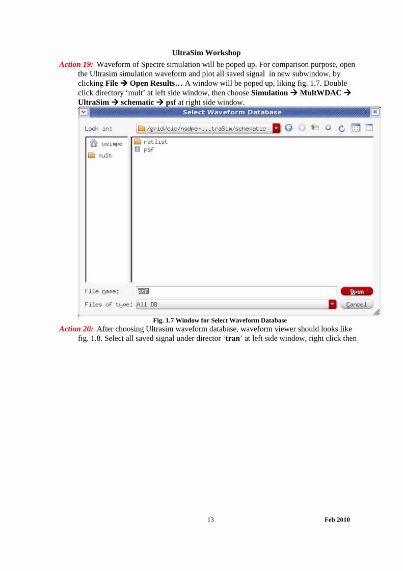
Action 19: Waveform of Spectre simulation will be poped up. For comparison purpose, open the Ultrasim simulation waveform and plot all saved signal in new subwindow, by clicking File ���� Open Results… A window will be poped up, liking fig. 1.7. Double click directory ‘mult’ at left side window, then choose Simulation ���� MultWDAC ���� UltraSim ���� schematic ���� psf at right side window.
Fig. 1.7 Window for Select Waveform Database
Action 20: After choosing Ultrasim waveform database, waveform viewer should looks like fig. 1.8. Select all saved signal under director ‘tran ’ at left side window, right click then

UltraSim Workshop
Feb 2010 14
choose ‘New Subwindow’ in poped menu.
Fig. 1.8 Waveform Viewer
Action 21: Resize the waveform window so that you can clearly see all the waveforms. In the
Waveform Window select Graph ���� Split Current Strip to separate the waveforms. Look at the output signals. These outputs should be virtually identical to those from the UltraSim simulation (see Fig.1.9). However, the Spectre simulation time is considerably longer.

UltraSim Workshop
Feb 2010 15
Fig. 1.9 Spectre and Ultrasim Simulation Result Comparison
Action 22: After reviewing the results, close ADE and the CIW windows by:
[ADE] Session ���� Quit In the Save State Query window, click No to dismiss it. [CIW] File ����Exit

UltraSim Workshop
Feb 2010 16
2. Using UltraSim in Analog Design Environment II Case Study: Simulating a PLL circuit In this case, we will simulate a PLL (phase locked loop) circuit using UltraSim within the Cadence analog design environment. Advanced features, such as setting UltraSim’s local options will be examined here. There are three sections in this case. In the first section, we will use the pre-layout netlist, add some UltraSim options, and compare the UltraSim simulation to a Spectre simulation. In the second section, we will use the same netlist, except that a verilogA behavioral model will replace the VCO (voltage-controlled oscillator) transistor level netlist. In the last section, we will use the post-layout netlist where we will study the effect of layout parasitics on the dynamic behavior of the PLL. Background: The PLL consists of a VCO, a digital frequency divider, a phase detector (PD), and a charge pump. The VCO generates eight 400MHz signals with different phases (p0, p45, p90… p315). One of the outputs (p0) is divided down by a factor of 2 before feeding into the phase detector (vcoclk). The other input to the phase detector is a 200MHz reference clock signal (refclk ). When the two inputs to the PD are out-of-sync, the PD will generate corrective pulses to adjust the differential output voltages of the charge pump (vcop, vcom), which control the frequency of the VCO. When the PLL is in lock, the signals vcoclk and refclk should be in phase, and the VCO control signals v(vcop) – v(vcom) should be stable. Note: If you did not finish the previous case (Using UltraSim in ADE I), please first read the setup section and correctly set up all the environmental variables. 2.1 Simulating the PLL using pre-layout netlist Action 1: Change to pll directory and start IC design framework.
% cd modules/pll Action 2: Start IC design framework
% virtuoso & Action 3: If the Library Manager window is already opened, jump to next step. Otherwise,
open the Library Manager window from the Command Interpreter Window (CIW).
[CIW] Tools ���� Library Manager…
UltraSim Workshop
Feb 2010 17
Action 4: In the Library Manager window, look for `amsPLL`, select:
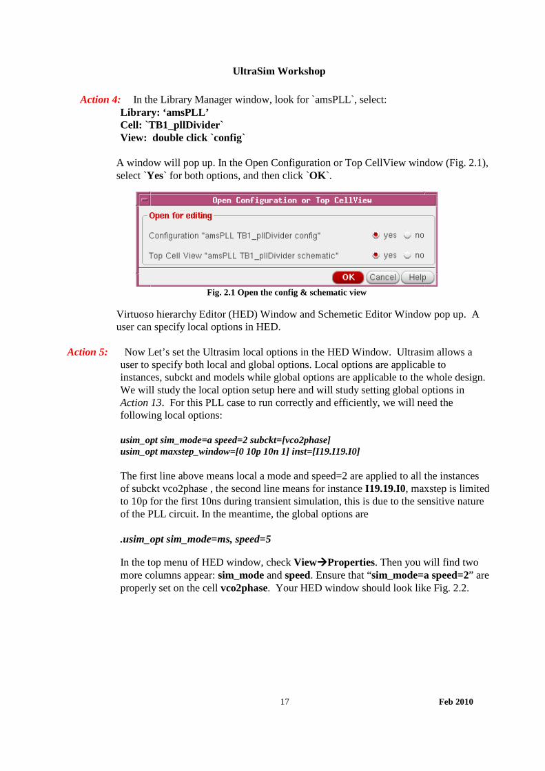
Library: ‘amsPLL’ Cell: `TB1_pllDivider` View: double click `config`
A window will pop up. In the Open Configuration or Top CellView window (Fig. 2.1), select Yes for both options, and then click `OK `.
Fig. 2.1 Open the config & schematic view
Virtuoso hierarchy Editor (HED) Window and Schemetic Editor Window pop up. A user can specify local options in HED.
Action 5: Now Let’s set the Ultrasim local options in the HED Window. Ultrasim allows a
user to specify both local and global options. Local options are applicable to instances, subckt and models while global options are applicable to the whole design. We will study the local option setup here and will study setting global options in Action 13. For this PLL case to run correctly and efficiently, we will need the following local options: usim_opt sim_mode=a speed=2 subckt=[vco2phase] usim_opt maxstep_window=[0 10p 10n 1] inst=[I19.I19.I0] The first line above means local a mode and speed=2 are applied to all the instances of subckt vco2phase , the second line means for instance I19.19.I0, maxstep is limited to 10p for the first 10ns during transient simulation, this is due to the sensitive nature of the PLL circuit. In the meantime, the global options are .usim_opt sim_mode=ms, speed=5
In the top menu of HED window, check View����Properties. Then you will find two more columns appear: sim_mode and speed. Ensure that “sim_mode=a speed=2” are properly set on the cell vco2phase. Your HED window should look like Fig. 2.2.

UltraSim Workshop
Feb 2010 18
Fig. 2.2 Local UltraSim options setup
If these are not there, you can add options in HED with the following steps: � In Table View, click Right Mouse Button (RMB) on the line of vco2phase, in
column sim_mode, choose a` from cyclic options. Then do the same thing to set `2` for `speed. (see Fig. 2.2)
� Save the UltraSim option: [Cadence hierarchy editor window] File ���� Save (Needed) � Look in the Messages section to ensure that the configuration was saved. In ADE,
you will have global UltraSim options for the whole circuit, but this block setting will overwrite the global settings for the specified block in the simulation
Note: � There are 7 simulation modes (S, A, MX, MS, DA, DF, DX) for choosing. The default
is MS mode Speed can be set between 1-8, the default is 5. For more information, please refer to the Ultrasim Manual.
� In case you want to set extra options besides sim_mode and speed for the blocks, you can do this: [Cadence hierarchy editor window] Edit ���� Add Property Column…

UltraSim Workshop
Feb 2010 19
Key in the Property Name and follow the same procedure mentioned above to key in the value. We could set the necessary local option “maxstep_window” here too. However maxstep_window is also an analysis timestep control option which is grouped under Analysis. In this lab we will set maxstep_window in Action 14. .
Action 6: In the Cadence HED window, switch to Tree View
[Cadence hierarchy editor window] View ���� Tree In the Tree View panel, confirm that the View to Use for pllDivider is schematic. If not, click Right Mouse Button (RMB) the line with the pllDivider entry and then select “Set Instance View����schematic”. Update and save the configuration by clicking View����Update and File����Save.
Now double click the line with the pllDivider entry to move down one level of hierarchy. Double click again on the line with the pll entry. Confirm that the View used for the cells pllDivider , pll and vco are all set to schematics. Otherwise change to schematic view and update the configuration. Then, click on I19����I19����I0 and look at I15, I16, I17, I18. (Fig.2.3), you should find the UltraSim options for each block. If not, go back and do Action 5 again.
Fig. 2.3 local options in HED window
Action 7: Now let us exam the schematics of the design. In the Virtuoso Schematic Editor
window, click Edit ���� Hierarchy ���� Descend Read. Click to select the cell pllDivider and open the schematic view. Following the same procedure, you can

UltraSim Workshop
Feb 2010 20
also push into the cell pll and then vco. After reviewing the PLL schematics, return to top by Edit ���� Hierarchy ���� Return to Top.
Action 8: Start the analog design environment, close the What’s New window that pops up
[Virtuoso Schematic Editor] Launch ���� ADE L Note: IC6.x provides three environments: ADE L/XL/GXL. ADE L is the basic ADE and supports basic analysis. ADE GXL is the most powerful ADE and supports all the functions. For more information, please refer to the ADE User Guide.
Action 9: Now load the simulator state.
[ADE] Session->Load State
In the Loading State window, select state1_prelayout and click OK . Action 10: In the ADE window, make sure you see the words Simulator:UltraSim.
Fig. 2.4 ADE window
Please note (Fig. 2.4) that the transient simulation time is 400n, and the plotted nodes or expressions in Outputs section, also, the Plotting mode is Replace.

UltraSim Workshop
Feb 2010 21
Action 11: Verify the model files under Setup ���� Model libraries … (Fig. 2.5). After viewing
the form, click Cancel to close it. Note the variable $FLOW is pre-defined in the environment setting up.
Fig. 2.5 Model Setup
Action 12: Double click on the ‘tran’ analysis line in the upper right hand corner of the ADE
window. The Choosing Analysis form pops up. (Fig. 2.6). Notice the transient analysis is set for 400ns.
Fig. 2.6 Choosing Analysis form
Click the Options… button at the lower right corner of the Choosing Analysis form and a Transient Options form pops up. You can find the Integration method is set to be euler. Then Cancel out of these forms.
Note: Integration method has 5 options. They are be, trap, traponly, gear2, gear2only. The default method for MS mode is be.
Action 13: Now let us set the global options.
[ADE] Simulation ���� Options ���� Analog …
These are some options about simulation mode, speed and postlayout. Refer to the UltraSim User Guide for more details on these options. Notice Ultrasim options are

UltraSim Workshop
Feb 2010 22
sorted into different tabs --- Main, Algorithm, Componet, PostLayout, Output, Checks and Miscellaneous.
For this case we are running the simulation in `Mixed Signal (MS) mode, with speed=5, Post-layout method is `No RCR (0) which means pre-layout mode (Main tab), DC method is set to Complete DC (1) (Algorithm tab) and Allow usim_opt on HED` option has been checked (Miscellaneous tab). The last one means the UltraSim options we saved previously in HED, will be included in the netlist. Next, switch to other tabs to look at other UltraSim options. At last, please click Cancel to quit both of the forms.
Note: DC integration method has 4 options, which are Skip DC (0), Complete DC (1), Fast DC (2), spectre DC (3). The default value for MS mode is Complete DC (1).
Action 14: As mentioned in Action 5, we are to set local maxstep option here.
[ADE] Analysis ���� Choose… The “Choosing Analysis” form pops up, click on Options… button. The “Transient Options” form pops up. Scroll down to the bottom of the popped up form and verify the maxstep_window is set to “0 10p 10n 1” and the applied subckt instance is I19.I19.I0.
Action 15: Verify initial condition. [ADE] Simulation->Convergence Aids->Initial Condition
The Select Initial Condition Set window pops up (Fig. 2.7)
Fig. 2.7 Initial condition

UltraSim Workshop
Feb 2010 23
The purpose of the ic statement is to initialize the VCO at a desirable state at the beginning of the transient. Most oscillators will need some kind of initial conditions to properly start the oscillation. Note: If initial condition is needed for additional nodes, you can first select the desired node in the schematic Window. If the node is selected, the node name will pop up in the “Node Set” Column in Select Initial Condition Set window (Fig. 2.7), then you can key in the voltage value for the selected node. Now you may close the Initial Condition window by clicking Cancel.
Action 16: Make sure spectre format netlist will be used for the simulation.
[ADE] Setup ���� Environment ���� Netlist Format
Note: UltraSim can read HSPICE format or Spectre format or mixed language netlist. This functionality allows the user to use either Hspice or Spectre netlists. UltraSim will call the appropriate netlister to netlist out in the appropriate format. However, this case has no hspiceD view for the circuits so we will only use spectre format.
Action 17: Generate the netlist.
[ADE] Simulation ���� Netlist ���� Recreate
ADE creates and displays the netlist. Note that the netlist is in the Spectre format. UltraSim accepts netlists in either HSPICE or Spectre format. Scroll to the end of the netlist and check the UltraSim options, the included model files, and make sure there is an ic (initial condition) statement. ic I19.I19.I0.inm2=2 net033=2
Action 18: Start the UltraSim simulation.
[ADE]: Simulation ���� Run … Note: You may get a dialogue box warning you about the need for data base conversion, this is a feature of IC61 enabling conversion to OA upon detection. Click “OK”
When the simulation is done, you may close the simulation log file window by clicking File ���� Close Window.
Action 19: A waveform window (Viva) will pop up (as Fig. 2.8 below). Also please look at the ADE window and you will see the freq expression is evaluated, the result is around 25MHz.

UltraSim Workshop
Feb 2010 24
Action 20: Read the lock time at which both vcop and vcom become flat. Also read the VCO
control voltage during lock. Find the value of vcop and vcom signals at time=300ns.
Lock time: ________ v(vcop):________ v(vcom):________ delta V:________
Fig. 2.8 Result in ViVa
Action 21: (optional) If time permits and you have the interest, it is possible to run Spectre on
the same case to compare the result and performance between Spectre and UltraSim. Just simply follow these steps:
[ADE]: Setup ���� Simulator/Directory/Host… Select Spectre for simulator then click OK In the Simulator/Directory/Host window change Simulator to Spectre and click OK . If the Save State Query window pops up, click No to close it. [ADE] Session ���� Load State… In the Loading State window, select state1 and click OK At the right lower corner, change the Plotting mode from Replace to Append.

UltraSim Workshop
Feb 2010 25
Note: Depending on the Viva default window size on your system, you may get a “New sub Window” instead of appended traces. In this case to see the trace overlays, simply create necessary sub Window by clicking Trace->New Graph->Copy New SubWindow, then click on a trace and then drag & drop onto the identical trace in the new subwindows to see comparisons like Fig. 2.9 below. [ADE] Simulation ���� Run …
For your reference, we have already done the simulation and here is the result: Runtime: Spectre: 7min14s UltraSim runs 1min11s. UltraSim is about 6X faster. Result: See Fig. 2.9, you can see the outputs of Spectre and UltraSim are almost the same.
Fig. 2.9 Comparison of Spectre and UltraSim results in prelayout simulation
(Red lines are results from Spectre)
After reviewing the results, close ADE window by
[ADE] Session ���� Quit

UltraSim Workshop
Feb 2010 26

UltraSim Workshop
Feb 2010 27
2.2 Simulating the PLL with VerilogA VCO model Action 22: Now we would like to re-simulate the PLL circuit, but using a VerilogA model for
the VCO. Open the Cadence Hierarchy Editor Window. (Skip this step if the Hierarchy Editor Window is already open)
[Virtuoso Schematic Editing Window] Hierarchy-Editor ���� Edit Configuration
Action 23: Change to the Tree View
[Cadence hierarchy editor window] View ����Tree
In the Tree View panel, search for `I0 (amsPLL vco schematic) under the pllDivider and pll entry. Right click the line, select “Set Instance View ���� veriloga”. (See Fig. 2.10)
Fig. 2.10 switch the view from schematic to behavioral VerilogA module

UltraSim Workshop
Feb 2010 28
Action 24: Update the configuration.
[Cadence Hierarchy Editor Window] View ���� Update
In the Update Sync-up window, select the cellview and click OK .
To explore the VerilogA model of the VCO, in the Virtuoso Schematic Editing window, click Edit ���� Hierarchy ���� Descend Read. Click to select the cell pllDivider and open the schematic view in current tab. Following the same procedures, you can also push into the cell pll and vco. This time a text window showing the VerilogA model will be displayed. After reviewing the model, close the text window and return to the top of design hierarchy by clicking Edit ���� Hierarchy ���� Return to Top.
Action 25: Start the analog design environment.
[Virtuoso Schematic Editor] Launch ���� ADE L Note: IC6.x provides three environments: ADE L/XL/GXL. ADE L is the basic ADE and supports basic analysis. ADE GXL is the most powerful ADE and supports all the functions. For more information, please refer to the ADE User Guide.
Action 26: Now load the pre-saved simulation state including the configurations to run the simulation.
[ADE] Session ���� Load State…
In the Loading State window, select state1_verilogA and click OK
Note: There is no need for an initial condition as in the previous example. The VCO VerilogA model can start to oscillate with no initial conditions.
Action 27: Double click on the ‘tran’ analysis line in the upper right hand corner of the ADE
window. Notice the transient simulation is set to be 400ns. Click the Options… button at the lower right corner of the “Transient Choosing” form, then the ‘Transient Options’ form pops up. You can find the Integration method is set to gear2only now. Then Cancel out of these forms.
Note: Integration method has 5 options. They are euler, trap, traponly, gear2, gear2only. The default value for MS mode is euler.

UltraSim Workshop
Feb 2010 29
Action 28: Look at some of the UltraSim options.
[ADE] Simulation ���� Options ���� Analog …
These are some of the simulation mode, speed and post-layout options. Refer to the UltraSim User Guide for more details on these options. Note starting from IC610, the Ultrasim options are sorted into different TABs. In this simulation we will use Mixed Signal (MS) mode, with speed=5, Post-layout method is No RCR (0) which means pre-layout mode (Main Tab), `DC method is set to Complete DC (1) (Algorithm tab). Next, please switch to other tabs to look at other UltraSim options. At last, please click Cancel to quit both of the forms. Note: DC integration method has 4 options, which are Skip DC (0), Complete DC (1), Fast DC (2), spectre DC (3). The default value is Complete DC (1).
Action 29: Generate the netlist.
[ADE] Simulation ���� Netlist ���� Recreate
ADE creates and displays the netlist. Scroll to the end of the netlist. You should see an ahdl_include statement that includes the VCO VerilogA model into the netlist. In addition, confirm that the initial condition is no longer there.
Close the netlist window by clicking File ���� Close Window
Action 30: Start the UltraSim simulation.
[Analog Circuit Design Environment] Simulation ���� Run …

UltraSim Workshop
Feb 2010 30
Action 31: Once the simulation is done, a waveform window will pop up. Resize the waveform window so that you can clearly see all the waveforms (See Fig. 2.11).
Fig. 2.11 output of simulation with verilogA module
Action 32: Read the lock time at which both vcop and vcom become flat. Also, read the VCO
control voltage during lock. Find the value of vcop and vcom signals at time=300ns. Read values of v(vcop) and v(vcom) at the lower edge of the window. Lock time: ________ v(vcop):________ v(vcom) ________ delta V:________ Compare the data with those from the last simulation.
Action 33: Now you may close the Waveform window and ADE window.
[Waveform Window] Window ���� Close [Analog Circuit Design Environment] Session ���� Quit

UltraSim Workshop
Feb 2010 31
2.3 Simulating the PLL using post-layout netlist
Action 34: Now we would like to simulate the PLL circuit again by using a netlist extracted
from the layout, which includes all the parasitic elements (R’s and C’s). If the HED window is open, skip this action. Otherwise, open the Cadence Hierarchy Editor Window:
[Virtuoso Schematic Editing Window] Hierarchy-Editor ���� Edit Configuration
Action 35: Change to the Tree View
[Cadence hierarchy editor window] View ���� Tree
In the Tree View panel, click Right Mouse Button (RMB) the line with the pllDivider entry. Select “Set Instance View ���� av_RC”. Update the configuration. [Cadence hierarchy editor window] View ���� Update In the Update Sync-up window, select the cellview and click OK .
Action 36: Start the analog design environment.
[Virtuoso Schematic Editor] Launch ���� ADE L Note: IC6.x provides three environments: ADE L/XL/GXL. ADE L is the basic ADE and supports basic analysis. ADE GXL is the most powerful ADE and supports all the functions. For more information, please refer to the ADE User Guide.
Action 37: Load the simulation state. Make sure the simulator is “UltraSim ”.
[Analog Design Environment] Session ���� Load State…
In the Loading State window, select state1_extractRC and click OK
Action 38: Review UltraSim options.
[Analog Circuit Design Environment] Simulation ���� Options ���� Analog … Note starting from IC610, the Ultrasim options are sorted into different TABs. We are running this simulation in `Mixed Signal (MS) mode, with 4` for speed setting and post-layout method setting (Liberal RCR(3)), which is postl=3 (Main tab). DC method is Complete DC (1)` (Algorithm tab). Switch to PostLayout tab you will see rshort and rvshort are set to 1 to speed up the simulation while maintaining the accuracy.

UltraSim Workshop
Feb 2010 32
Note: DC method has 4 options, which are Skip DC (0), Complete DC (1), Fast DC (2), spectre DC (3). The default value is Complete DC (1).
Action 39: Double click on the ‘tran’ analysis line in the upper right hand corner of the ADE
window. The transient time is set to be 400ns. Click the Options… button at the lower right corner in the “Transient Choosing” form, then the ‘Transient Options’ form pops up. Then Cancel out of these forms.
Note: Integration method has 5 options. They are euler, trap, traponly, gear2, gear2only. The default value for MS mode is euler.
Action 40: Generate the netlist.
[Analog Circuit Design Environment] Simulation ���� Netlist ���� Recreate ADE creates and displays the netlist. This netlist is much longer and you should see all the extracted RC parasitic components.
Action 41: Start UltraSim simulation.
[Analog Circuit Design Environment] Simulation ���� Run … Action 42: Once the simulation is done, a waveform window will pop up. Also please look at
the ADE window and you will see the freq expression is evaluated, the result is around 25M (See Fig. 2.12)
Fig. 2.12 Postlayout simulation
Action 43: You may not see the oscillations in vcom and vcop as shown above. This is due to
accuracy and time step control. We need tighter time step control to see the oscillations
Note: At this point, your waveforms may not look like this… Read on…

UltraSim Workshop
Feb 2010 33
as shown in Fig. 2.11. We can do this by choosing a lower speed (which would slow the entire simulation) or use the maxstep option to limit the maximum time step the simulator can take (which will slow the simulation even more) or use the powerful maxstep_window feature to only provide for accurate time step control where needed. By designer experience we know that the following command will give you the oscillations: .usim_opt maxstep_window=[0 10p 10n 100p] Note this local option is more conservative than the previous maxstep_window. You set the new maxstep_window as below
1) [ADE] simulation����options����analog
2) On the ADE analog options form: Select the Misc Tab (far right) ,Scroll to the bottom to “Other USIM Options”
3) The maxstep_window option, as appears above without the “.usim_opt” in the field
under “Other Options”:”Other USIM Options”.
4) If you added maxstep_window as above, then OK the analyses forms
Now you can re-run the simulation. [Analog Circuit Design Environment] Simulation ���� Run …
Action 44: Read the lock time at which both vcop and vcom become flat. Also read the VCO
control voltage during lock. Find the value of vcop and vcom signals at time=300ns. Lock time: ________ v(vcop):________ v(vcom) ________ delta V:________
Compare the data with those from the pre-layout simulation. You should be able to observe that the post-layout simulation yielded a much larger VCO control voltage, v(vcop)-v(vcom), than the pre-layout simulation. This is because the layout RC parasitic significantly reduces the gain (Kvco) of the VCO, which is defined as the sensitivity of the output frequency to the control voltage. The bandwidth of the PLL depends on the gain of the VCO. Thus, the layout parasitic will also reduce the bandwidth of the PLL. An indirect consequence is the increase of lock time, as revealed by the UltraSim simulation results. This example demonstrates that UltraSim is a powerful tool to study the time-domain characteristics of a PLL, especially when a post-layout netlist is used.

UltraSim Workshop
Feb 2010 34
Action 45: Close everything and exit Virtuoso.
[Waveform Window] File ���� Close [Analog Circuit Design Environment] Session ���� Quit [Cadence Hierarchy editor] File ���� Exit [Virtuoso Schematic Editing] Window ���� Close [CIW] File����Exit
Note: To restart the simulation, you can type ./CLEAN to remove all the output file.
UltraSim Workshop
Feb 2010 35
3 Using Digital Vector Files
You can define digital input stimuli or vectors in a digital vector file. UltraSim converts the input vectors into PWL voltage sources. If the expected digital outputs are included in the digital vector file, UltraSim will also check simulated outputs against the expected values. Additionally, starting at MMSIM6.1 and later, UltraSim supports hierarchical VEC.
3.1 Simulating a 16-bit multiplier with digital vector file
Action 1: Change to the mult16_vec directory.
% cd modules/mult16_vec Action 2: Look at the multiplier netlist file, mult16.net.
% more mult16.net The multiplier has one 16-bit input (B<15:0>), a clock input (CLK ), and a 32-bit output (P<31:0>). In the module mult16x16, there is another 16-bit input as A<15:0> and these inputs are specified in the vector file mult16_vec.vec.
Action 3: Look at the digital vector file, mult16_vec.vec.
% more mult16_vec.vec radix 4444 4444 44444444 io iiii iiii oooooooo vname X1.A<[15:0]> B<[15:0]> P<[31:0]> hier 1 tunit ns The first few lines define the properties of the vector signals. “radix ” defines the number of bits in each vector, “io” specifies directions (input, output or bidirectional) of signals, “vname” specifies signal names. Please note for A<15:0>, vname is set as X1. A<15:0>. This is because there are no ports for A<15:0> in the top level netlist. The user needs to specify the full path to use hierarchical vectors. “hier 1” tells UltraSim to interpret the “.” in the vname as hierarchical delimiter. If “hier” is set to 0, then UltraSim will regard X1.A as a node name and “.” is not treated as a hierarchical delimiter. “tunit ” is for time unit. “trise” and “tfall ” are for input rise and fall times. “vih”, “ vil ”, “ voh”, and “vol” specify input high voltage, input low voltage, output high voltage, and output low voltage respectively.

UltraSim Workshop
Feb 2010 36
The majority portion of the vector file mult16_vec.vec is the tabular data. Each line in the tabular data section consists of the absolute time point and the values of all the defined vectors. Note: 1. The first two output vectors are ”xxxxxxxx”, which are “don’t care”. The multiplication result of the first input vectors is the third output vector. 2. Default value for hier is 1 in vec file.
Action 4: Now let us look at the top-level netlist file, mult16_vec.sp.
% more mult16_vec.sp
Please pay attention to .vec card, .lprobe card and the wild card character (*) used in the .lprobe cards. The vector file is specified by the .vec card. The logic probe (.lprobe) will be examined in Action 5. Also notice that the Digital Fast (DF) simulation mode is chosen through the option sim_mode=df speed=8. For digital circuits, either the digital fast (for functional verification) or the digital accurate (for timing verification) may be used. Note: There are 7 simulation modes (S, A, MX, MS, DA, DF, DX) for selection. The default is MS mode. Speed can be set between 1-8, the default is 5)
Action 5: Often it is easier to use digital probe “lprobe” on digital blocks. Let us look at the input file mult16_vec.sp again. The lprobe statement set up the logic probes for all the nodes on the top level: .lprobe tran low=1.25 high=1.25 v(*) depth=1 The lprobe converts the analog output waveforms into digital waveforms, which significantly reduces the size of the output waveform file. The low= value and high= value arguments define the threshold values for the analog to digital conversion. Both the regular probe and lprobe statements can contain hierarchical names and wild card character “* ” for nodes or elements. The depth=value argument specifies the depth in the circuit hierarchy that a wildcard name is applied. If set as “1”, only the nodes at the top level are selected. User can also set vl and vh in .usim_opt statement to define the global low and high value.
Action 6: Run an UltraSim simulation and wait until the simulation completes.
% ultrasim +log mult16_vec.out mult16_vec.sp or % ./run

UltraSim Workshop
Feb 2010 37
Note: By using “+log”, you can have the output log printed both on screen and to the file you specified. There are two other options for output log. They are “=log” which means only print log to the file the user specified and “-log” which means only print log to the screen. In this case, you will see the log printed on the screen and finally, UltraSim indicates a successful simulation by echoing to the screen "UltraSim completed successfully.”.
Action 7: View the vector checking results.
% more mult16_vec.veclog All the outputs P<31> ~ P<0> should be correct. If any matching error occurs, an error file will be generated. Note: Search in the run directory for waveform files named mult16_vec.vecexp and mult16_vec.vecerr. By them, UltraSim provides a new way to view the expected vectors and vector errors in graphic besides opening the error file in text editor. This feature will be very helpful to see the difference between the simulation results and expected outputs in VEC/VCD/EVCD files.
Checking waveform with SimVision Action 1: Start the waveform viewer.
% simvision &
The SimVision Design Browser window appears. Action 2: Open waveform database by using a previously saved command script.
[SimVision: Design Browser] File ���� Source Command Script… Action 3: In the “Select SimVision Command Script” window, select file mult16_vec.sv and
click Open.
All the input and output waveform should be seen. In addition, output vectors defined in VEC file and vector errors are displayed in simvision. Note the v(vec_err), means vector error, is 0 throughout the whole simulation, which indicates there is no error in comparing output signals to expected vectors.

UltraSim Workshop
Feb 2010 38
Fig. 3.1 Output of Multi16_vec.sp
Action 4: Exit SimVision and prepare for the next lab.
[SimVision: Design Browser] File ���� Exit SimVision or, [SimVision: Waveform 1] File ���� Exit SimVision Click “Yes” in the “SimVision Exit” window.
Note: To restart the lab, type ./CLEAN to remove all the output files.

UltraSim Workshop
Feb 2010 39
3.2 Using VCD/EVCD Files UltraSim can also take VCD (Value Change Dump) files and EVCD (Extended Value Change Dump) files as digital input stimuli and check expected digital outputs. A VCD/EVCD file is usually generated by a Verilog simulator (VerilogXL, NCSim, etc). Note, starting from MMSIM6.0USR2 and later, UltraSim supports hierarchical VCD/EVCD. EVCD is an extension of VCD and is defined in IEEE1364. Compared to VCD, the signal value in EVCD contains not only logic value, but also port direction and driver strength. Additionally, EVCD has two sets of states for INPUT and OUTPUT respectively that can represent more information about the state and strength of the signal. The support for VCD and EVCD are fully compatible. The VCD and EVCD from the same Verilog netlist can share the same signal info file. In this lab, we will simulate the same case with stimuli file in VCD or EVCD format and compare the results.
3.3 Simulating a small case with VCD file
Action 1: Change to the vcd_hier directory
% cd modules/vcd_hier
Action 2: Take a look at the top-level netlist file, vcd_hier.sp
% more vcd_hier.sp Notice the VCD file is invoked by .vcd 'vcd_hier.vcd' 'vcd_hier.info' The .vcd card contains both the VCD file name “vcd_hier.vcd” and the associated signal info file “vcd_hier.info”. The signal info file contains the information: signal name mapping, definition of high and low voltages, rise and fall time, the attribute (in/out/bi) of the signals. View the hierarchical structure of analog netlist to understand how to map VCD name and analog name in VCD signal information file.
Action 3: Take a look at the VCD file, vcd_hier.vcd
% more vcd_hier.vcd The file contains the Definition Section and the Data Section. In the Definition Section, the time scale is defined as 100fs, which is also the time unit for VCD signal information file. The names of all the vectors are defined in the same section. Please note that these names are described in full hierarchical structure starting from top level. $scope and $upscope end statements are paired to describe the hierarchical structure. The Data

UltraSim Workshop
Feb 2010 40
Section contains the time points and values of all the vectors. This case provides an example of hierarchical VCD file.
Action 4: Take a look at the VCD signal information file, vcd_hier.info
% more vcd_hier.info
Action 5: Check the alias definition in VCD signal information file The statement “.hier 1 ” sets hier to 1 means the VCD file contains hierarchical vector names. The signal name in VCD signal information file belongs to VCD name space. Alias statements convert signals with full path in VCD file to the corresponsive signals in analog netlist. For examples, .alias top.* * .alias top.level1_block2.P7 Xp7.P7
Action 6: Check the signal direction definition in VCD signal information file For hierarchical VCD mapping, the full path needs to be specified in .scope statement. For the .bi statement, the enable signal must contain the hierarchical path because the signal may belong to a different scope. For multiple .scope statements, the effective scope of each .scope statement is affected by the other statements, requiring the .in, .out, and .bi statements to be in the correct location.
Look at the enable signal definition of bi-direction signal. The enable signal can be from analog netlist and VCD file. For example, .bi '~ (top.level1_block2.p6 ^ X6_mid) & IN6 & top.level1_block1.p5 & X6_mid' p3 If a VCD signal is used as an enable signal, it must be declared an input using the .in statement and located in the VCD file. In the above example, only signal, top.level1_block1.p5, is from VCD file, and the rest is from analog netlist. Even for the analog enable signal, User still need .alias statement for name mapping.
Action 7: Take a look at the definitions for periodic check window and check ignore
Setting the period argument activates periodic window checking. The following statement defines periodic check window for signal “ top.level1_block2.p7”. .chkwindow -1e+3 5e+3 1 period=10000 first=12000.1 top.level1_block2.p7 .chk_ignore specifies a window used to ignore output vector checks for a VCD file. The following statement defines time window to ignore vector check for signal “top.level1_block2.p6”. .chk_ignore 0 5e+6 top.level1_block2.p6
UltraSim Workshop
Feb 2010 41
Action 8: Run UltraSim simulation
% ultrasim +log vcd_hier.out vcd_hier.sp
Action 9: View the vector checking results.
% more vcd_hier.veclog You can play with statements “.chkwindow” and “.chk_ignore” and check vcd_hier.veclog again. Note: Search in the run directory for waveform files named vcd_hier.vecexp and vcd_hier.vecerr. By them, UltraSim provides a new way to view the expected vectors and vector errors in graphic besides opening the error file in text editor. This feature will be very helpful to see the difference between the simulation results and expected outputs in VEC/VCD/EVCD files.
Checking waveform with SimVision Action 1: Start the waveform view
% simvision& Action 2: Open waveform database by using a previously saved command script
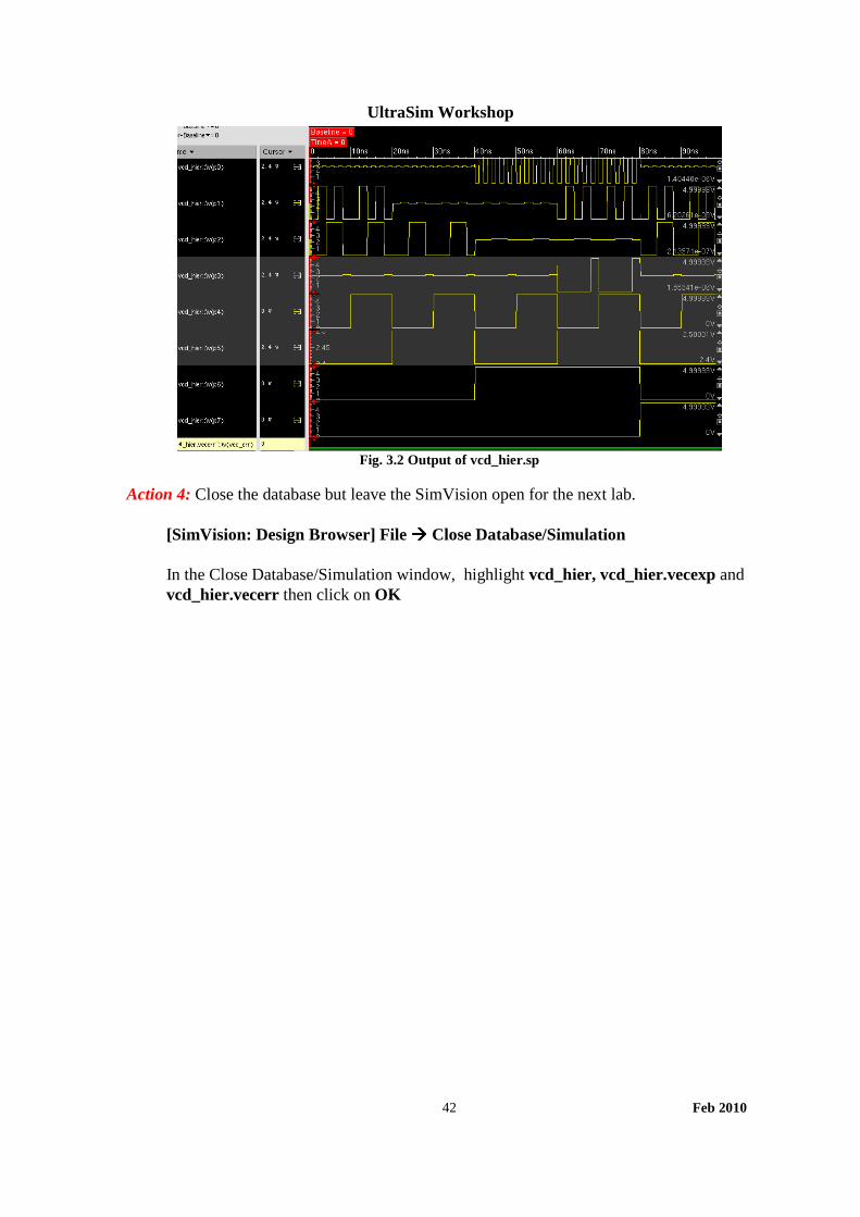
[SimVision: Design Browser] File ���� Source Command Script… Action 3: In the “Select SimVision Command Script” window, select file vcd_hier.sv and click Open. We are able to inspect the signals from VCD file. p0, p1, p2, and p3 are bi-direction signal (Fig. 3.2) The voltage rails from 0V to 5V means they are in OUTPUT stage, otherwise they are in INPUT stage. At the last, it is seen the v(vec_err) means vector error, has the value 0 throughout the simulation which indicates there is no violation in vector check.
In addition, the vcd_hier_vecexp waveform is also opened so feel free to plot the expected outputs and compare with the real outputs.
UltraSim Workshop
Feb 2010 42
Fig. 3.2 Output of vcd_hier.sp
Action 4: Close the database but leave the SimVision open for the next lab.
[SimVision: Design Browser] File ���� Close Database/Simulation In the Close Database/Simulation window, highlight vcd_hier, vcd_hier.vecexp and vcd_hier.vecerr then click on OK

UltraSim Workshop
Feb 2010 43
3.4 Simulating the same case with EVCD file Action 1: Make a new netlist that will use EVCD stimuli file
% cp vcd_hier.sp evcd_hier.sp Action 2: Edit the newly created file. You will see:
.vcd 'vcd_hier.vcd' 'vcd_hier.info' *.evcd 'evcd_hier.evcd' 'vcd_hier.info'
Uncomment .evcd statement and comment out .vcd statement. Note we will use the same signal _info file. The new netlist evcd_hier.sp should have these statements: *.vcd 'vcd_hier.vcd' 'vcd_hier.info' .evcd 'evcd_hier.evcd' 'vcd_hier.info'
Action 3: Take a look at the EVCD file, evcd_hier.evcd.
% more evcd_hier.evcd
The syntax of EVCD is quite similar to VCD. While comparing the two data files, you can find out that there are two major differences as follows: • The syntax to specify the node information ($var statement)
For example, in EVCD data file: $var port 1 ! p0 $end Here only "port" is used to define the type of variable. The rest is the same.
• The syntax of the value change and the strength definition in EVCD file.
For example: pH 0 6 % Here "p" is a key character which indicates a port. "H" is a state character which contains information of the driving direction and the value of port. "H" stands for OUTPUT port with "High" state. "0 6" defines the strength. The first number indicates the strength0 component of the value and the second one indicates the strength1 component of the value. The value of the strength varies from 0 to 7. "%" is an identifier code for the port which was defined in the $var construct for the port
Note: This is also a hierarchical EVCD file. There is same scope and name definition as those in VCD file. Therefore it matches the signal info file as well.

UltraSim Workshop
Feb 2010 44
Action 4: Run UltraSim simulation.
% ultrasim +log evcd_hier.out evcd_hier.sp
Action 5: View the vector checking results.
% more evcd_hier.veclog Note: Search in the run directory for waveform files named evcd_hier.vecexp and evcd_hier.vecerr. By them, UltraSim provides a new way to view the expected vectors and vector errors in graphic besides opening the error file in text editor. This feature will be very helpful to see the difference between the simulation results and expected outputs in VEC/VCD/EVCD files.
Checking waveforms with SimVision Action 1: Go back to SimVision. Open waveform database by using a previously saved
command script
[SimVision: Design Browser] File ���� Source Command Script… Action 2: In the “Select SimVision Command Script” window, select file evcd_hier.sv and
click on Open, a waveform like figure 3.3 will show up. It is easily to observe the result of vcd and evcd simulations are the same. At the last, the v(vec_err), means the vector error, can be seen at 0 throughout the simulation. It indicates there is no violation for the vector check.
Fig. 3.3 Output of evcd_hier.sp

UltraSim Workshop
Feb 2010 45
Action 3: Exit SimVision and prepare for the next lab
[SimVision: Design Browser] File ���� Exit SimVision, or [SimVision: Waveform 1] File ���� Exit SimVision Click “Yes” in the “SimVision Exit” window.
Note: To restart the simulation, you can type ./CLEAN to remove all the output files.

UltraSim Workshop
Feb 2010 46
4 Using Structural Verilog Netlists UltraSim supports the use of structural Verilog netlists for verification of digital circuits. The most common approach is to use a top level Spice file which contains the analysis statement, probe, measure, and simulation control options, which also calls one or multiple Verilog netlist files. Use the ultrasim –vlog command line flag to utilize this feature. Please refer to the UltraSim User Guide for details. You can also include Verilog files by using the .vlog_include statement, as shown in this example. 4.1 Simulating a multiplier with structural Verilog netlist Action 1: Change to the mult16_vlog directory.
% cd modules/mult16_vlog Look for three netlists in this directory: mult16_vlog.sp Top level Spice netlist mult16.v Structural Verilog netlist mult16_lib.spi Transistor level netlist
Action 2: Look at the Verilog netlist mult16.v. The top level module is top, which is a 16 bit
multiplier, structurally identical to the one used in the last two examples. top calls other lower level modules such as NAND2, OAI21, AND2, INV, etc.
Action 3: Look at the transistor level netlist mult16_lib.spi. This file contains Spice netlist for
all the basic cells called by the Verilog modules in mult16.v .
Action 4: Now look at the top level Spice netlist mult16_vlog.sp. Pay attention to these two statements: .vlog_include mult16.v supply0=gnd! supply1=vdd! insensitive=yes .include mult16_lib.spi The first statement causes UltraSim to read the Verilog file mult16.v. The ground node used for the Verilog subcircuit is defined by supply0, and the power node is defined by supply1. If insensitive=1, the Verilog netlist is parsed case insensitive. The second statement simply includes the file mult16_lib.spi into the top level netlist.

UltraSim Workshop
Feb 2010 47
Please note in this simulation, the UltraSim options we will set are sim_mode=DF and speed=8. Note: There are 7 simulation modes (S, A, MX, MS, DA, DF, DX) for selection. The default is MS mode. Speed can be set between 1-8, the default is 5).
Action 5: Run UltraSim
% ultrasim +log mult16_vlog.out mult16_vlog.sp or % ./run
Action 6: View the vector checking results. % more mult16_vlog.veclog You should get all outputs P<31> ~ P<0> correct. If any errors occur, an error file will be generated.
Note: Search in the run directory for waveform files named mult16_vlog.vecexp and mult16_vlog.vecerr. By them, UltraSim provides a new way to view the expected vectors and vector errors in graphic besides opening the error file in text editor. This feature will be very helpful to see the difference between the simulation results and expected outputs in VEC/VCD/EVCD files.
Checking waveforms with SimVision
Action 1: Start the waveform viewer.
% simvision &
Action 2: Open waveform database using a previously saved command script.
[SimVision: Design Browser] File ���� Source Command Script…

UltraSim Workshop
Feb 2010 48
Action 3: In the “Select SimVision Command Script” window, select file mult16_vlog.sv and click Open. All the input and output waveform should be seen. In addition, output vectors defined in VEC file and vector errors are displayed in simvision. Note the v(vec_err), means vector error, is 0 throughout the whole simulation which indicates there is no error in comparing output signals to expected vectors.
Fig. 4.1 Output of Multi16_vlog.sp
Action 4: Exit SimVision.
[SimVision: Design Browser] File ���� Exit SimVision, or [SimVision: Waveform 1] File ���� Exit SimVision Click “Yes” in the “SimVision Exit” window.
Note: To restart the simulation, you can type ./CLEAN to remove all the output files.

UltraSim Workshop
Feb 2010 49
5 Hierarchical versus Flat Mode Simulation
Case Study: Simulating a 16Kb SRAM UltraSim is a fast, high capacity, transistor level simulator. UltraSim’s speed and capacity are due to the hierarchical capabilities that are at the core of UltraSim. UltraSim will look at all the subcircuits that are the same and then look at the stimulus being driven into these subcircuits. Multiple subcircuits with similar stimulus will be simulated as one subcircuit instead of many subcircuits. This brings tremendous efficiency to the simulation in the form of reduced memory utilization and increased performance while maintaining accuracy. This efficiency can not be realized with flat mode simulators.
hier=0 Flatten the netlist (default in S, A, AMR mode) hier=1 Auto-detect hierarchy (default in DF, DA, MS modes)
5.1 Running flat mode simulation on a 16Kb SRAM
Action 1: Change to sram16k directory.
% cd modules/sram16k Action 2: Look at the SRAM netlist file, sram16k.net.
% more sram16k.net
This SRAM circuit has 1024x16 bit of memory cells, 10-bit address input (A<9:0>), 16-bit data input (DI<15:0>), 16-bit data output (DO<15:0>), pre-charge input (PRE) and write/read control (WR, 1=write, 0=read).
Action 3: Look at the top-level netlist file, sram16k.sp.
% more sram16k.sp
Note that the simulation mode is set to flat by the option hier=0. The input stimuli are provided by the included digital vector file “sram16k.vec”. The same file also provides the expected outputs. 16 write cycles and 16 read cycles will be simulated with an end time of 3200ns. You will see these statements in the netlist: .usim_opt hier=0 .usim_opt sim_mode=df speed=3 Note: There are 7 simulation modes (S, A, MX, MS, DA, DF, DX) for selection. The default is MS mode. Speed can be set between 1-8, the default is 5).

UltraSim Workshop
Feb 2010 50
Action 4: Run UltraSim simulation.
% ultrasim +log sram16k.out sram16k.sp Action 5: View vector checking results.
% more sram16k.veclog You should get all outputs (DO<15> ~ DO<0>) correct. Note: Search in the run directory for waveform files named sram16k.vecexp and sram16k.vecerr. By them, UltraSim provides a new way to view the expected vectors and vector errors in graphic besides opening the error file in text editor. This feature will be very helpful to see the difference between the simulation results and expected outputs in VEC/VCD/EVCD files.
Action 6: Check total CPU time and memory usage. % more sram16k.out The total CPU time and memory usage can be found at the end of the file. Write down these numbers. Flat mode: CPU Time: ___________ Max. Memory Usage: ___________
Checking waveform with SimVision Action 1: Start the waveform viewer.
% simvision & Action 2: Open waveform database using a previously saved command script.
[SimVision: Design Browser] File ���� Source Command Script… Action 3: In the “Select SimVision Command Script” window, select file sram16k.sv and
click Open.
All the input and output waveform should be seen. In addition, output vectors defined in VEC file and vector errors are displayed in simvision. Note the v(vec_err), means vector error, is 0 throughout the whole simulation which indicates there is no error in comparing output signals to expected vectors.

UltraSim Workshop
Feb 2010 51
Fig. 5.1 Output of sram16k.sp
Action 4: Exit SimVision.
[SimVision: Design Browser] File � Exit Simvision, or [SimVision: Waveform 1] File � Exit Simvision Click “Yes” in the “SimVision Exit” window.
5.2 Running hierarchical simulation on the 16K SRAM Action 1: Create a new input file.
% cp sram16k.sp sram16k_hier.sp Action 2: To switch from flat mode to hierarchical mode, make the following change to
sram16k_hier.sp with any text editor:
.usim_opt hier = 0 ���� .usim_opt hier = 1
The option hier = 1 will cause UltraSim to automatically detect the circuit hierarchy, which will naturally invoke hierarchical simulation for hierarchical netlist.
Action 3: Run UltraSim simulation.
% ultrasim +log sram16k_hier.out sram16k_hier.sp Action 4: View vector checking results.
% more sram16k_hier.veclog
You should get all outputs (DO<15> ~ DO<0>) correct.
Note: Search in the run directory for waveform files named sram16k_hier.vecexp and sram16k_hier.vecerr. By them, UltraSim provides a new way to view the expected vectors and vector errors in graphic besides opening the error file in text editor. This feature will be very helpful to see the difference between the simulation results and expected outputs in VEC/VCD/EVCD files.

UltraSim Workshop
Feb 2010 52
Action 5: Check total CPU time and memory usage.
% more sram16k_hier.out The total CPU time and memory usage can be found at the end of the file. Compare these numbers with the results from the flat simulation. Hierarchical mode: CPU Time: ___________ Max. Memory Usage: ___________ You may view the waveforms using Simvision follow the same procedure as in the last section. Just need to source sram16k_hier.sv instead of sram16k.sv . The waveform should be the same and no vector error will be seen.
5.3 Other UltraSim options
In this example the UltraSim options sim_mode=DF and speed=3 are used. In general DF or DA modes are recommended for most SRAM, DRAM, or ROM circuits. The option speed=3 is chosen to achieve better accuracy than the default setting of speed=5, in the expense of slight increase of simulation time. The users are encouraged to try different options of sim_mode and speed to experiment the trade-off between accuracy and simulation speed.
Note: To restart the lab, type ./CLEAN to remove all the output files.
UltraSim Workshop
Feb 2010 53
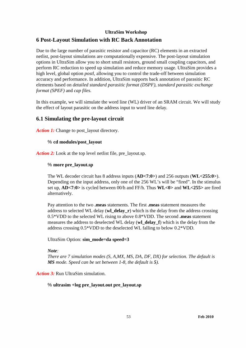
6 Post-Layout Simulation with RC Back Annotation Due to the large number of parasitic resistor and capacitor (RC) elements in an extracted netlist, post-layout simulations are computationally expensive. The post-layout simulation options in UltraSim allow you to short small resistors, ground small coupling capacitors, and perform RC reduction to speed up simulation and reduce memory usage. UltraSim provides a high level, global option postl, allowing you to control the trade-off between simulation accuracy and performance. In addition, UltraSim supports back annotation of parasitic RC elements based on detailed standard parasitic format (DSPF), standard parasitic exchange format (SPEF) and cap files. In this example, we will simulate the word line (WL) driver of an SRAM circuit. We will study the effect of layout parasitic on the address input to word line delay.
6.1 Simulating the pre-layout circuit Action 1: Change to post_layout directory.
% cd modules/post_layout Action 2: Look at the top level netlist file, pre_layout.sp. % more pre_layout.sp
The WL decoder circuit has 8 address inputs (AD<7:0>) and 256 outputs (WL<255:0>). Depending on the input address, only one of the 256 WL’s will be “fired”. In the stimulus set up, AD<7:0> is cycled between 00/h and FF/h. Thus WL<0> and WL<255> are fired alternatively. Pay attention to the two .meas statements. The first .meas statement measures the address to selected WL delay (wl_delay_r) which is the delay from the address crossing 0.5*VDD to the selected WL rising to above 0.8*VDD. The second .meas statement measures the address to deselected WL delay (wl_delay_f) which is the delay from the address crossing 0.5*VDD to the deselected WL falling to below 0.2*VDD. UltraSim Option: sim_mode=da speed=3 Note: There are 7 simulation modes (S, A,MX, MS, DA, DF, DX) for selection. The default is MS mode. Speed can be set between 1-8, the default is 5).
Action 3: Run UltraSim simulation. % ultrasim +log pre_layout.out pre_layout.sp

UltraSim Workshop
Feb 2010 54
Action 4: Check the measurement results
%more pre_layout.meas0
Write down the values of wl_delay_r and wl_delay_f. Pre-layout simulation: wl_delay_r = _________, wl_delay_f = _________,
Checking pre-layout waveforms with SimVision
Action 1: Start the waveform viewer.
% simvision& Action 2: Open waveform database using a previously saved command script.
[SimVision: Design Browser] File ���� Source Command Script… Action 3: In the “Select SimVision Command Script” window, select file pre_layout.sv and
click Open.
You can now inspect the waveforms of the top level signals
Fig. 6.1 Output of pre_layout.sp
Action 4: Leave the SimVision open for the next lab

UltraSim Workshop
Feb 2010 55
6.2 Simulating the post-layout netlist with DSPF parasitic RC file
Action 1: Look at the post-layout netlist file, post_layout_dspf.sp. % more post_layout_dspf.sp Basically the post-layout netlist is the pre-layout netlist plus the following new UltraSim options: .usim_opt postl=1 spf=decoder.spf The UltraSim option postl is for controlling the trade-off between simulation accuracy and performance. postl=0 (default) is designated for simulation of pre-layout netlist . UltraSim does not perform RC filtering or reduction. postl=1,2,3, 4 are intended for post-layout simulation. As the postl level gets higher, UltraSim applies more aggressive RC reduction, resulting in much smaller run time and memory usage at the cost of slightly degraded simulation accuracy. The option spf = file-name will stitch a DSPF file which consists the extracted RC parasitics.
Action 2: Take a look at dspf file. % more decode.spf
Notice the header of the file looks like
*|DSPF 1.3
*|DESIGN dec
*|DIVIDER /
*|DELIMITER :
The first line *|DSPF indicates this is a file of DSPF format. The second line *|DESIGN is the extracted cell name. The third line *|DIVIDER specifies the hierarchical delimiter used in the extraction tool. *|DELIMITER specifies the terminal deliminter. DSPF files usually have two sections: net section and instance section. Net section has the interconnect parasitics for each net, for example
*|NET AD<5> 0.00168539PF *|P (AD<5> B 0 0.54 1.38) *|I (XPRE1/XINV1<2>/XN0/M0:GATE XPRE1/XINV1<2>/XN0/M0 GATE I 1.95e-16 5.35 2.035) *|I (XPRE1/XINV1<2>/XP0/M0:GATE XPRE1/XINV1<2>/XP0/M0 GATE I 4.68e-16 2.14 2.035) Cg1 AD<5>:1 0 3.27182e-16 Cg2 XPRE1/XINV1<2>/XN0/M0:GATE 0 9.96914e-17 Cg3 XPRE1/XINV1<2>/XP0/M0:GATE 0 5.59194e-17

UltraSim Workshop
Feb 2010 56
Cg4 AD<5>:2 0 3.40996e-16 Cg5 AD<5> 0 8.61606e-16 R1 AD<5>:1 AD<5>:2 6.46018 R2 AD<5>:1 AD<5> 13.5762 R3 AD<5>:1 XPRE1/XINV1<2>/XN0/M0:GATE 180.917 R4 AD<5>:1 XPRE1/XINV1<2>/XP0/M0:GATE 296.747 R5 XPRE1/XINV1<2>/XN0/M0:GATE AD<5>:2 174.321
Statements starting with *|P and *|I describes NET AD<5>’s connectivities to the devices. The statements starting with R and C describes the RC network.
Instance section usually appears at the bottom of the DSPF file, it includes all the devices with layout specific parameters. For example
* Instance Section * MXPOST0/XI0/XI0/XINV1/XN0/M0 XPOST0/XI0/XI0/XINV1/XN0/M0:DRN + XPOST0/XI0/XI0/XINV1/XN0/M0:GATE VSS VSS NMOS ad=0.136p as=0.136p l=0.13u + pd=1.48u ps=1.48u w=0.4u MXPOST0/XI0/XI0/XINV1/XP0/M0 VDD XPOST0/XI0/XI0/XINV1/XP0/M0:GATE + XPOST0/XI0/XI0/XINV1/XP0/M0:SRC VDD PMOS ad=0.35p as=0.19p l=0.13u pd=3.4u + ps=1.76u w=1u USIM can stitch not only the net section (parasitic RCs) but also the instance section.
Action 3: Run UltraSim simulation. % ultrasim +log post_layout_dspf.out post_layout_dspf.sp
Action 4: Check the stitching result. USIM reports detailed stitching results in *.spfrpt file and log file. Let us check the relevant information in the log file first
% more post_layout_dspf.out
Notice the statistic information regarding stitching ------------------------------------------------------------------------------- Nets | parsed 1089 | expanded 1088 | not expanded 0 Capacitors | parsed 12990 | expanded 12714 | Resistors | parsed 25741 | expanded 25465 | New nodes | added 12935 | | ------------------------------------------------------------------------------- nets stitched with C-only 0 nets stitched with RC 41 skip nets 1
------------------------------------------------------------------------------- As you can see, 1088 nets out of 1089 nets are stitched with RCs. The skipped net is net “EN” as indicated in post_layout_dspf.spfrpt file, which contains more detail on stitching results.
Action 5: Let us exam post_layout_dspf.spfrpt file.

UltraSim Workshop
Feb 2010 57
% more post_layout_dspf.spfrpt
Notice quite some warnings regarding some small resistors are removed. In general, when there is mismatch between dspf file and the prelayout netlist, USIM would issue a warning if the mismatch can be corrected by the stitching engine, or an error if the mismatch can not be corrected. A user has control over how USIM handles the mismatches. By default, USIM tries to stitch as many parasitic RCs as possible and only discards the unmatched ones.
Action 6: Check the measurement results
% more post_layout_dspf.meas0 Write down the values of wl_delay_r and wl_delay_f. Post-layout simulation: wl_delay_r = _________, wl_delay_f = _________,
Checking post-layout waveforms with SimVision
Action 1: Open waveform database using a previously saved command script.
[SimVision: Design Browser] File ���� Source Command Script…
Action 2: In the “Select SimVision Command Script” window, select file dspf.sv and click Open.
You can now inspect the waveforms of the top level signals. (Fig. 6.2)
Action 3: Leave the SimVision open for the next lab
Fig. 6.2 Output of pre_layout.sp and pre_layout netlist with DSPF file

UltraSim Workshop
Feb 2010 58
6.3 Simulating the post-layout circuit with the SPEF parasitic RC file
Action 1: Copy the file post_layout_dspf.sp into a new file post_layout_spef.sp.
% cp post_layout_dspf.sp post_layout_spef.sp
Action 2: Open the new file with any editor and change the line .usim_opt postl=1 spf=decoder.spf to .usim_opt postl=1 spef=decoder.spef Save the file. The option spef = file-name will stitch a SPEF file consisting the extracted RC parasitic.
Action 3: let us exam the spef file. % more decoder.spef
Notice the header of the spef file:
*SPEF "IEEE 1481-1998" *DIVIDER / *DELIMITER : *BUS_DELIMITER [] *T_UNIT 1 NS *C_UNIT 1 FF *R_UNIT 1 OHM *L_UNIT 1 HENRY
The first line *SPEF specifies that this file is of spef format. *DIVIDER specifies the hierarchical delimiter while *DELIMITER specifies the terminal delimiter. *BUS_DELIMITER specifies the bus delimiter symbols. *T_UNIT , *C_UNIT , *R_UNIT and *L_UNIT specifies the unit for RCL. In this SPEF file, name mapping is used. For example
*NAME_MAP
*51 Z\<19\>
*52 Z\<16\>
*53 Z\<17\>
*54 Z\<18\>

UltraSim Workshop
Feb 2010 59
*55 Z\<0\>
Name Mapping mechanism can significantly reduce the file size. SPEF files contain only the interconnect parasitics. It does not contain device informations.
The interconnect parasitic information are grouped by D_NET. For example
*D_NET *331 1.68539
*CONN
*P *331 B *C 0.54 1.38
*I *5150:GATE I *C 5.35 2.035 *L 0.195
*I *5151:GATE I *C 2.14 2.0
*CAP
1 *331:10214 0.327182
2 *5150:GATE 0.0996914
*RES
1 *331:10214 *331:10208 6.46018
2 *331:10214 *331 13.5762
*END
Action 3: Run UltraSim simulation. % ultrasim +log post_layout_spef.out post_layout_spef.sp
Action 4: Just like in the last lab, USIM outputs statistic information regarding stitching in the log file and in a *.spfrpt file. Examine both files and then close both files.
Action 5: Check the measurement results
% more post_layout_spef.meas0 Write down the values of wl_delay_r and wl_delay_f. Post-layout simulation: wl_delay_r = _________, wl_delay_f = _________

UltraSim Workshop
Feb 2010 60
Checking post-layout waveforms with SimVision
Action 1: Open waveform database using a previously saved command script. [SimVision: Design Browser] File ���� Source Command Script…
Action 2: In the “Select SimVision Command Script” window, select file spef.sv and click
Open.
Fig. 6.3 Output of pre_layout.sp and the comparison of pre_layout netlist with DSPF/SPEF file
You will see 9 separated signals. Group the signals from DSPF simulation and SPEF simulation, [SimVision: Waveform 1] Edit ���� Create ���� Analog Overlay
Highlight them in pairs, then you will see the similar output as Fig.5.3
Action 3: Exit SimVision.
[SimVision: Design Browser] File ���� Exit Simvision, or [SimVision: Waveform 1] File ���� Exit Simvision Click “Yes” in the “SimVision Exit” window.
Compare post-layout measurement results to the pre-layout results
Compare the measurement results from the last three simulations. You will discover the impact of the layout RC parasitic on the address to WL delays. For memory design, a key design parameter is the read access time. The address to WL delay is an important component of the read access time. This example clearly demonstrates that UltraSim is an indispensable tool in designing high density and high performance memories.

UltraSim Workshop
Feb 2010 61
6.4 Resistor and Capacitor Statistical Checks Action 1: uncomment the following lines in the file post_layout_dspf.sp .usim_report resistor type=distr rmin=0 rmax=1G .usim_report capacitor type=distr cmin=0 cmax=1
These two statements invoke the Resistor and Capacitor Statistical Checks, which will report the distribution of resistor or capacitor values within the user-defined range. The following options are supported:
• type=warning prints a warning about large resistors (capacitors) and reports the number of resistors (capacitors) with values above rmax (cmax).
• type=distr prints resistor (capacitor) statistics into a xxxx.chk_resistor (xxxx.chk_capacitor) log file for resistors (capacitors) with values between rmin (cmin) and rmax (cmax).
• type=print prints resistors (capacitors) with values between rmin (cmin) and rmax (rmin) into a xxxx.chk_resistor (xxxx.chk_capacitor) log file.
The Resistor and Capacitor Statistical Check syntax are: .usim_report resistor type=warning rmax=value .usim_report resistor type=distr rmin=value rmax=value .usim_report resistor type=print rmin=value rmax=value nlimit=num sort=[dec|inc] .usim_report capacitor type=warning cmax=value .usim_report capacitor type=distr cmin=value cmax=value .usim_report capacitor type=print cmin=value cmax=value nlimit=num sort=[dec|inc] Action 2: Run UltraSim simulation.
% ultrasim +log post_layout_dspf.out post_layout_dspf.sp
Action 3: Open the output files post_layout_dspf.chk_resistor and post_layout_dspf.chk_capacitor to examine the distribution of the parasitic RC values. Action 4: For next user’s benefit, please un-do action 1 by commenting out the following two lines .usim_report resistor type=distr rmin=0 rmax=1G .usim_report capacitor type=distr cmin=0 cmax=1 in File post_layout_dspf.sp Note To restart the lab, type ./CLEAN to remove all the output files.

UltraSim Workshop
Feb 2010 62
7 UltraSim Power and Design Analyses This example demonstrates the following UltraSim analysis methods: Dynamic Checks
• Power Checking Analysis performs over current, voltage, and high impedance node checks.
• Node Activity Analysis provides information about the nodes and monitors activity such as voltage overshoot (VO) and voltage undershoot (VU).
• Design Checking Analysis monitors device voltages during simulation. • Active Node Checking Analysis detects nodes with voltage changes that exceed the user-
defined threshold. • Hot Spot Node Current Check provides the info of the average charging and average
discharging current statistics for the specified nodes over the checking window • Dynamic Power Analysis reports the power consumed by each element and subcircuit in
the design. Static Checks The circuit in this example is a high voltage charge pump with an internal oscillator. The function is to generate a high voltage output (VPP) by pumping up the power supply (VDD). 7.1 Simulating a high voltage charge pump
Action 1: Change to the pump directory.
% cd modules/pump Action 2: Look at the top level netlist file, pump.sp.
% more pump.sp
The pump circuit has an enable input (EN), an analog input to control the oscillator frequency (VOSC) and a high voltage output (VPP). The loading of the pump consists of a resistor (10kohm) and a capacitor (10pF) connected in parallel. At the end of the netlist are several analysis related statements. We shall first simulate the circuit and view the waveforms. Then we will walk through each of the analysis statements. UltraSim Options: sim_mode=a
Note: There are 7 simulation modes (S, A, MX, MS, DA, DF, DX) for selection. The default is MS mode. Speed can be set between 1-8, the default is 5).
Action 3: Run UltraSim simulation.
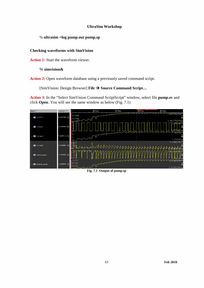
UltraSim Workshop
Feb 2010 63
% ultrasim +log pump.out pump.sp
Checking waveforms with SimVision
Action 1: Start the waveform viewer.
% simvision& Action 2: Open waveform database using a previously saved command script.
[SimVision: Design Browser] File ���� Source Command Script…
Action 3: In the “Select SimVision Command ScriptScript” window, select file pump.sv and click Open. You will see the same window as below (Fig. 7.1)
Fig. 7.1 Output of pump.sp

UltraSim Workshop
Feb 2010 64
7.2 Probing voltage or current of an element or subcircuit
Action 1: Open the file pump.sp again.
% more pump.sp
Action 2: Find the following three probe statements near the end of the file:
.probe tran v(CK1) v(VPP)
.probe tran i1(RL)
.probe tran x(X5.VDD) The first statement probes the voltage waveform at nodes CK1 and VPP. The second statement probes the current flowing through the load resistor RL , which is equal to the output current of the charge pump. The third statement probes the current flowing into the instance X5 through the VDD node. Here X5 is the actual charge pump block excluding the oscillator. The current x(X5.VDD) includes the current flowing into all the lower hierarchical subcircuits under X5 through the global VDD node. If the currents flowing into the subcircuits below X5 are to be excluded, then the syntax x0(X5.VDD) can be used. The output waveforms created by these three probe statements are stored in the output files pump.trn and pump.dsn.
Action 3: Review the waveforms v(ck1), v(vpp), and i1(rl) in the Simvision Waveform window (Fig. 7.1).

UltraSim Workshop
Feb 2010 65
7.3 Probing power of a subcircuit
Action 1: Look for the following two probe statements in the file pump.sp:
.probe tran input_power = par (`v(VDD) * i1(VDD)`)
.probe tran output_power = par (`v(VPP) * i1(RL)`) These two statements invoke the Dynamic Power Analysis of UltraSim. The first statement probes the input power of the pump which is defined as the product of v(VDD) and the current flowing into the global node VDD. The second statement probes the output power of the pump which is defined as the product of v(VPP) and the current flowing into the load resistor RL . The output waveforms created by these two probe statements are stored in the output files pump.expr.trn and pump.expr.dsn.
Action 2: Review the waveforms ‘input_power’ and ‘output_power’ in the Simvision Waveform window (Fig. 7.1).
Action 3: Exit SimVision.
[SimVision: Design Browser] File ���� Exit SimVision , or [SimVision: Waveform 1] File ���� Exit SimVision Click “Yes” in the “SimVision Exit” window.

UltraSim Workshop
Feb 2010 66
7.4 Using Dynamic Power Analysis to calculate the efficiency of the pump
Action 1: Look for the following three measure statements in the file pump.sp:
.measure tran avg_input_power avg `v(VDD) * i1(VDD)` from=400n to=500n
.measure tran avg_output_power avg `v(VPP) * i1(RL) from=400n to=500n
.measure tran efficiency = ` avg_output_power / avg_input_power`
.option measdgt = 6 The first two statements invoke the Dynamic Power Analysis of UltraSim. The first one computes the average input power of the pump, whereas the second one computes the average output power of the pump. The third statement is a regular measure statement that calculates the efficiency of the pump based on the results generated by other measure statements. The measurement results are stored in the output files pump.meas0 and pump.mt0. It is very common to use .measure statement in the simulation since it outputs ASCII result which is easy to compare by designers. In order to provide more accurate information from .measure, UltraSim supports measdgt option. Please note the 4th statement above is to set 6 digits shown in the .meas0 and .mt0 file. The default value will be 4 digits.
Action 2: Open the file pump.meas0 and observe the measurement results. Note the very low
efficiency, which is typical for a small on-chip charge pump.

UltraSim Workshop
Feb 2010 67
7.5 Power Analysis on a subcircuit
Action 1: Look for the following statement in the file pump.sp
.usim_pa pa_subckt subckt sort=avg power=on time_window=[400n 500n] This statement is used to set up power analysis on all the subcircuits. It reports the average, maximum, and RMS current at all the ports of subcircuits. In addition, the argument power=on requests UltraSim to report the average, maximum, and RMS power consumed by all the subcircuits. The results are sorted in the decreasing order of the average values. The start and stop time of the checking window can be set. The analysis results are stored in the output file pump.pa. The usim_pa command has options to select any number of subcircuits and ports for measurement of current and power consumption. Please refer to the UltraSim User Guide for more details.
Action 2: Open the file pump.pa and review the measurement results. Look at the section of Port Power Summary. Add up the average power consumptions of all theports ‘*.vdd’, and compare the result with the value of avg_input_power reported in pump.meas0.

UltraSim Workshop
Feb 2010 68
7.6 Node activity analysis
Action 1: Look for the following line in the file pump.sp: .usim_nact nact1 limit=10 type=max_vu sort=dec node=[x1.* x2.*] .usim_nact nact2 limit=10 type=max_vo sort=dec stop=150n param=[max_vo max_vu]
This command sets up a Node Activity Analysis on all the nodes of the circuit. This analysis monitors for each node • Maximum and average voltage overshoot (VO) /undershoot (VU) • Maximum and minimum rise / fall time • Signal probability of being high and low • Capacitance • Number of toggles. The analysis results are printed to a file named pump.nact. Multiple statements are supported and the results will be printed according to the order of the usim_nact statement. The first statement set the analysis only on the nodes belong to subckt x1 and x2. Arguments type=max_vu sort=dec causes UltraSim to sort the nodes in the output file in the decreasing order of max_vu. Any output parameters can be selected for sorting, in either the descending or ascending order. The argument limit = 10 causes UltraSim to print out the 10 nodes that rank highest, according to the specified criterion. If the limit is not specified, then data for all the nodes are printed to the file. The second statement sets the specific check window from 0 to 150n and will list 10 nodes that have highest overshoot voltage, and only mx_vu and max_vo are listed.
Action 2: Open the file pump.nact and review the analysis results.

UltraSim Workshop
Feb 2010 69
7.7 Node Glitch Analysis Action 1: Look for the following line in the file glitch.sp:
.usim_nact nact1 analysis=glitch sort=max_vu node=n2 numlevel=100 tth=2n
This command sets up the node glitch analysis for the specified nodes. Node glitch analysis detects glitches in reference to static voltage levels of a signal. This analysis is performed as follows:
• Static voltage levels (where the voltage level is constant) at the specified nodes are determined.
• All static levels below 0.5V are considered as static low level. • All static levels above 0.5V are considered as static high level. Ultrasim detects overshoot glitches in reference to static low level and undershoot glitches in reference t static high level.

UltraSim Workshop
Feb 2010 70
The analysis results are printed to a file named glitch.nact_glitch. The report contains one line for all glitches occurring during one static level. If one signal has multiple static levels and each static level contains glitches, one line is reported for each static level. The following parameters are reported for the glitches of each static voltage level:
• avg: Specifies the average glitch voltage level, that is, the average of maximum value of all glitches within one static level.
• max: Specifies the maximum glitch voltage level, that is, the voltage level of the maximum glitch within the static level.
• t_max: Specifies the time of the maximum glitch. • t_recovery: Specifies the time taken by the signal to recover from the glitch. • staticVal: Specifies the static voltage level. • vpp: Specifies the differeence between high and low static levels used to
calculate glitch threshold based on relative tolerances. • start: Specifies the start time of the static voltage level. • end: Specifies the end time of the static voltage level.
The report can be sorted based on overshoot glitches, undershoot glitches, average glitch voltage level, and maximum glitch voltage level. In addition, the values can be arranged in increasing or decreasing order. Overshoot glitches can be identified in the report by the reported static low level (below/equal to 0.5V). Undershoot glitches can be identified in the report by the reported static high level
Action 2: Run Ultrasim simulation. % ultrasim +log glitch.out glitch.sp Action 3: Open the file glitch.nact_glitch and review the analysis results. .TITLE 'This file is :./glitch.nact_glitch' ********.usim_nact-glitch nact1 ******** nodename glitch t_glitch t_rec overy staticVal Vpp ------- ------- ------- ------- ------- ------- o0_n2_s0 1.72251 1.3696e-07 1.3707e-07 3.00609 3.00683 o0_n2_s1 1.67365 2.34272e-07 2.34408e-07 3.0077 3.01033 o0_n2_s2 1.67309 4.53296e-07 4.53441e-07 3.00541 3.00977 o0_n2_s3 1.6699 2.09931e-07 2.10043e-07 3.00827 3.01409…
UltraSim Workshop
Feb 2010 71
A snap-shot of node n2 showing the glitches:

UltraSim Workshop
Feb 2010 72
7.8 Power Checking Analysis
Action 1: Look for the following two statements in the file pump.sp:
.pcheck ovicheck exi elem=[*] ith=1e-4 tth=10n preserve=all
.pcheck ovvcheck exv node=[*] vmin=0 vmax=4.99 tth=10n option=0 time_window=[300n 500n] .pcheck hizcheck zstate node=[*] ztime=50n
These three statements invoke the Power Checking Analysis function of UltraSim. The first pcheck statement contains the keyword exi, which makes UltraSim to report in an output file (pump.pcheck) which elements over what time period have current over the threshold (ith ) for a time period equal to or greater than the specified duration (tth ). The argument i(*) specifies that all the elements will be checked. The argument i(*) can be replaced by a list of elements or instance names to limit the scope of the check. The second pcheck statement contains the keyword exv, which makes UltraSim to report in an output file (pump.pcheck) which nodes over what time period have voltage over the threshold (vmax) for a time period equal to or greater than the specified duration (tth ). option has some special meanings. If option=0 which is default, Ultrasim reports any of the specified nodes with voltages above vmax or below vmin for a duration time longer than tth. However if option=1, UltraSim reports any of the specified nodes if its voltage falls between vmin and vmax for a duration time longer than tth. The third pcheck statement contains the keyword zstate, which causes UltraSim to report in an output file (pump.pcheck) which nodes over what time period were in high-z state for a time period equal to or greater than the specified duration (ztime). The argument v(*) specifies that all the nodes will be checked. The argument v(*) can be replaced by a list of nodes to limit the scope of the check. In the above two forms of pcheck statement, it is possible to specify the start and stop time of the checking window, as well as other checking criterion. Please refer to the UltraSim User Guide for more details.
Action 2: Open the output file pump.pcheck. Look for the elements which have a maximum operating current of more than 0.1mA. Also look for the nodes which have been floating for more than 50ns during the simulation.
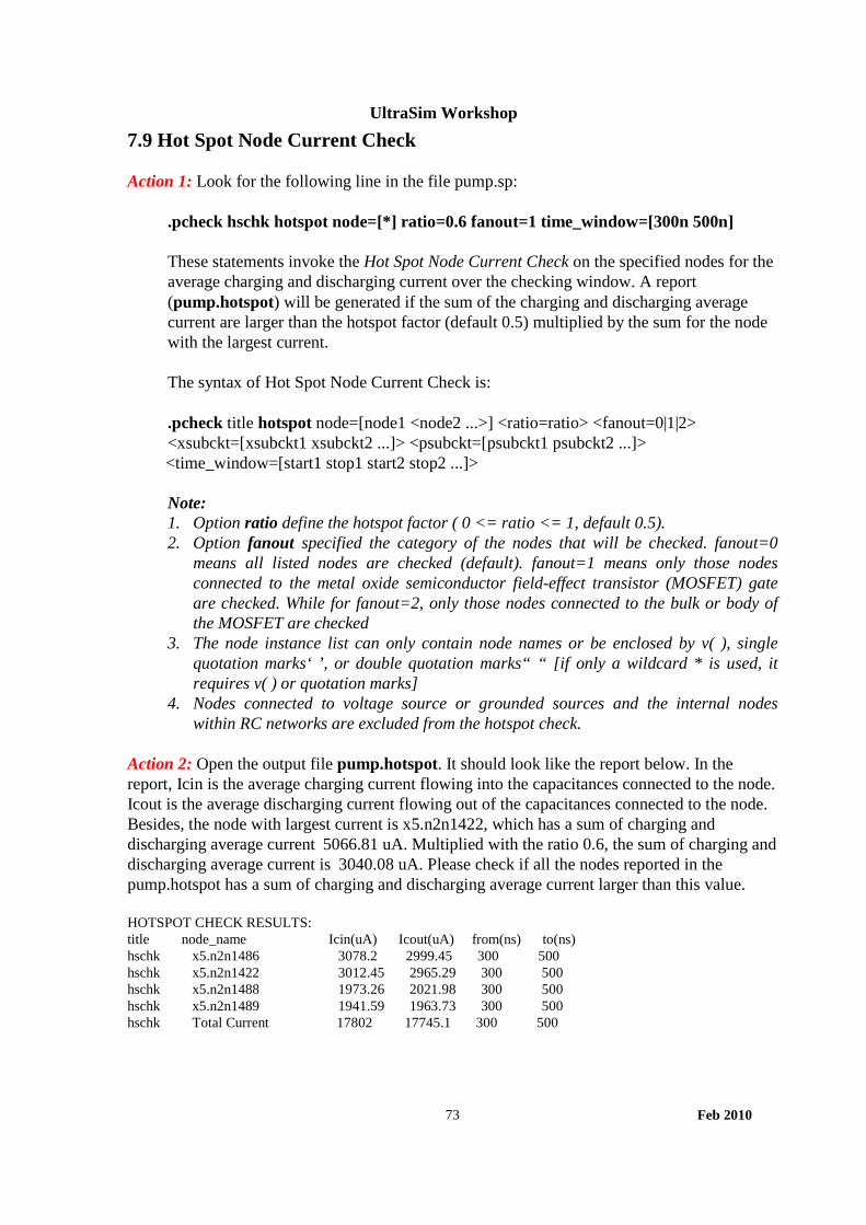
UltraSim Workshop
Feb 2010 73
7.9 Hot Spot Node Current Check Action 1: Look for the following line in the file pump.sp:
.pcheck hschk hotspot node=[*] ratio=0.6 fanout=1 time_window=[300n 500n] These statements invoke the Hot Spot Node Current Check on the specified nodes for the average charging and discharging current over the checking window. A report (pump.hotspot) will be generated if the sum of the charging and discharging average current are larger than the hotspot factor (default 0.5) multiplied by the sum for the node with the largest current. The syntax of Hot Spot Node Current Check is: .pcheck title hotspot node=[node1 <node2 ...>] <ratio=ratio> <fanout=0|1|2> <xsubckt=[xsubckt1 xsubckt2 ...]> <psubckt=[psubckt1 psubckt2 ...]>
<time_window=[start1 stop1 start2 stop2 ...]> Note: 1. Option ratio define the hotspot factor ( 0 <= ratio <= 1, default 0.5). 2. Option fanout specified the category of the nodes that will be checked. fanout=0
means all listed nodes are checked (default). fanout=1 means only those nodes connected to the metal oxide semiconductor field-effect transistor (MOSFET) gate are checked. While for fanout=2, only those nodes connected to the bulk or body of the MOSFET are checked
3. The node instance list can only contain node names or be enclosed by v( ), single quotation marks‘ ’, or double quotation marks“ “ [if only a wildcard * is used, it requires v( ) or quotation marks]
4. Nodes connected to voltage source or grounded sources and the internal nodes within RC networks are excluded from the hotspot check.
Action 2: Open the output file pump.hotspot. It should look like the report below. In the report, Icin is the average charging current flowing into the capacitances connected to the node. Icout is the average discharging current flowing out of the capacitances connected to the node. Besides, the node with largest current is x5.n2n1422, which has a sum of charging and discharging average current 5066.81 uA. Multiplied with the ratio 0.6, the sum of charging and discharging average current is 3040.08 uA. Please check if all the nodes reported in the pump.hotspot has a sum of charging and discharging average current larger than this value.
HOTSPOT CHECK RESULTS: title node_name Icin(uA) Icout(uA) from(ns) to(ns) hschk x5.n2n1486 3078.2 2999.45 300 500 hschk x5.n2n1422 3012.45 2965.29 300 500 hschk x5.n2n1488 1973.26 2021.98 300 500 hschk x5.n2n1489 1941.59 1963.73 300 500 hschk Total Current 17802 17745.1 300 500

UltraSim Workshop
Feb 2010 74
7.10 Design Checking Analysis (Device Voltage Check)
Action 1: Look for the following line in the file pump.sp:
.dcheck mosdvchk vmos model=NMOS vgdu=7 vgsu=7 vgbu=7 vdsu=7 duration=1n xinst=[x3 x4] .dcheck bjtdvchk vbjt model=NPN vceu=5 duration=1n time_window=[400n 500n] .dcheck resdvchk vres vpnu=7 duration=1n time_window=[300n 500n] .dcheck capdvchk vcap vpnu=5 duration=1n time_window=[300n 500n] .dcheck diodvchk vdio vpnl=-1.5 duration=1n *.dcheck mosdvchk vmos model=NMOS cond='vgd>7||vgs>7||vgb>7||vds>7' duration=1n *.dcheck bjtdvchk vbjt model=NPN cond='vce>5' duration=1n time_window=[400n 500n] *.dcheck resdvchk vres cond='vpn>7' duration=1n time_window=[300n 500n] *.dcheck capdvchk vcap cond='vpn>5' duration=1n time_window=[300n 500n] *.dcheck diodvchk vdio cond='vpn<-1.5' duration=1n *.dcheck mosdvchk_mix vmos model=PMOS cond='vgd<0.5||vds<0.5' vdsl=-3 duration=1n
These statements invoke the Design Checking Analysis on the voltages of mosfets, bjts, resistors, capacitors, and diode. UltraSim supports the design checking analysis on 6 types of component. Besides the above 5 types, there is another one JFET/MESFET supported in the new release. All the device voltages will be monitored during a simulation run. A report (pump.dcheck) will be generated if the voltages exceed the specified upper and lower bounds for a period longer than the specified duration. Note user can do the Design Voltage Check in three ways: 1. Conventional way: the conventional way is to use keywords (vgdu, vgsu, vdgl…) in
the statement. 2. Conditional way: the conditional way provides a more flexible method to perform
the check with complex expressions. The conditional expression supports the following operators: <, >, <=, >=, ==, ||, &&, and the following variables: vgs, vgd, vgd, vds, vdb, vsb, l, w. In addition, the expressions can be a combination of linear and/or nonlinear expressions.
3. Mixed way: user can put both conditional expression keywords (vgdu, vgsu, vdgl…) in one statement. UltraSim will filter the elements by the conditional expression and then check the violations with the keyword criteria.
Action 2: Open the file pump.dcheck. Find the NMOS transistors with detailed information
which have inter-terminal voltages larger than 7V during the simulation. And as well the reports about exceeded voltages on bjts, resistors and capacitors.
Action 3: copy the pump.dcheck to pump.dcheck.reg

UltraSim Workshop
Feb 2010 75
Action 4: Reopen pump.sp, comment out regular dcheck statements (adding * in the front of the statements) and uncomment the conditional dcheck statements (removing * in the front of the statements)
Action 5: Re-run UltraSim simulation.
% ultrasim +log pump.out pump.sp
Action 6: Open again the file pump.dcheck. Comparing with the file pump.dcheck.reg, you will see the same result.
Action 7: copy the pump.dcheck to pump.dcheck.con Action 8: Reopen pump.sp, comment out conditional dcheck statements (adding * in the front
of the statements) and uncomment the mixed dcheck statements (removing * in the front of the statements). It should like as:
.dcheck mosdvchk_mix vmos model=PMOS cond='vgd<0.5||vgs<0.5' vdsl=-3
duration=1n This is to check if the pmos mosfets with vds less than -3V meet the condition of having vdg or vgs less than 0.5V. User can try other combinations if interested.
Action 9: Re-run UltraSim simulation.
% ultrasim +log pump.out pump.sp
Action 10: Open again the file pump.dcheck. Check the results comparing with that in the file pump.dcheck.reg and file pump.dcheck.con.

UltraSim Workshop
Feb 2010 76
7.11 Active Node Checking Analysis
Action 1: Look for the following line in the file pump.sp: .acheck actchk node=[*] dv=5 inactive=2 time_window=[0 300n] This statement invokes the Active Node Checking Analysis. UltraSim detects nodes with voltage changing that exceed the user-defined threshold (dv). The Active Check Analysis syntax is: .acheck title node=[node1 node2 ...] <depth=value> dv=val <exclude=[node3 node4 ...] time_window=[start1 stop1 start2 stop2 ...] <inactive=0|1|2> Note: There are some options that user can set to control the behavior of Active Node Checking Analysis. exclude option is used to exclude some nodes from the check. While inactive=0|1|2 means only active nodes, or only inactive nodes, or both active nodes and inactive nodes are reported. In this case we will output both active nodes and inactive nodes during time from 0 to 300ns. The active nodes are listed in the pump.actnode and pump.actnodelist file. While inactive nodes are listed in pump.inactnode and pump.inactnodelist file.
Action 2: Open the files pump.actnode, pump.actnodelist, pump.inactnode and pump.inactnodelist. Note that most of the nodes with voltage swing larger than 5V are located in X5, which is the actual charge pump stage.

UltraSim Workshop
Feb 2010 77
7.12 Netlist Parameter Check Action 1: Look for the following line in the file pump.sp:
.usim_report chk_param wamaxmosw=50u waminmosl=0.5u This statement invokes the Netlist Parameter Check, which is one of the Static checks. This command checks whether the element size and simulation temperature are in the reasonable range or not and will issues warnings or errors according to the threshold values. The Netlist Parameter Check syntax is: .usim_report chk_param <ermaxcap=v> <wamaxcap=v> <ermincap=v> <wamincap=v> <ermaxres=v> <wamaxres=v> <erminres=v> <waminres=v> <ermaxmosw=v> <wamaxmosw=v> <erminmosw=v> <waminmosw=v> <ermaxmosl=v> <wamaxmosl=v> <erminmosl=v> <waminmosl=v> <ermaxmosas=v> <wamaxmosas=v> <ermaxmosad=v> <wamaxmosad=v> <ermaxmosps=v> <wamaxmosps=v> <ermaxmospd=v> <wamaxmospd=v> <ermaxmostox=v> <wamaxmostox=v> <erminmostox=v> <waminmostox=v> <ermaxdiodew=v> <wamaxdiodew=v> <ermindiodew=v> <wamindiodew=v> <ermaxdiodel=v> <wamaxdiodel=v> <ermindiodel=v> <wamindiodel=v> <ermaxdiodea=v> <wamaxdiodea=v> <ermindiodea=v> <wamindiodea=v> <ermaxtemp=v> <wamaxtemp=v> <ermintemp=v> <wamintemp=v> <erminfactor=v> <waminfactor=v> <model=m>
Action 2: Open the output file pump.rpt_chkpar . It should look like below:
model Subckt Parameter Limits Instancenmos vco_50m l=370.00n ( < 500.00n ) x1.mn1i1051 nmos vco_50m l=370.00n ( < 500.00n ) x1.mn1i1055 …

UltraSim Workshop
Feb 2010 78
7.13 Substrate Forward Bias Check Action 1: Look for the following line in the file pump.sp:
.usim_report chk_substrate sub_check mode=2 tth=1n This statement invokes the Substrate Forward Bias Check, which is one of the Static checks. This command checks whether a MOSFET substrate becomes forward biased. Note this command ONLY checks MOSFET substrate, but NOT other PN junctions. This check can be performed before DC initialization and/or during transient simulation. During transient simulation, a warning message is issued when the MOSFET substrate junction is forward biased by more than a threshold voltage (vt) AND the junction current is more than a threshold current (ith).
The Substrate Forward Bias Check syntax is: .usim_report chk_substrate title mode=[2|1|0] <num=n> <vt=v> <ith=iv> <start=t1> <stop=t2> <model=m>
Note when mode is 2, every MOSFET substrate connection is checked before DC calculation and during transient simulation. Mode equal to 1 means check in transient only and mode 0 means check before DC only.
Action 2: Open the output file pump.rpt_chksubs. It should seem like below:
****** MOS Substrate Forward Biased Before DC ****** Total of 4 Warnings reported Model Subckt Vb Source Instance pmos cp_enh2 0.0000e+00 v_x5_out x5.mp1i1441 pmos cp_enh2 0.0000e+00 v_x5_out x5.mp1i1444 pmos cp_enh2 0.0000e+00 v_x5_out x5.mp2i1441 pmos cp_enh2 0.0000e+00 v_x5_out x5.mp2i1444 ****** MOS Substrate Forward Biased During Simulation ****** Total of 5 Warnings reported Title Model Subckt Time EndTime Vb Vs Vd Ibs Ibd Instance sub_check pmos cp_enh2 2.4773e-08 2.9486e-08 1.9945e+00 2.4945e+00 1.9945e+00 0.0000e+00 0.0000e+00 x5.mp2i1444 sub_check pmos cp_enh2 2.4773e-08 2.9486e-08 1.9945e+00 2.4945e+00 1.9945e+00 0.0000e+00 0.0000e+00 x5.mp2i1441 sub_check pmos cp_enh2 2.4773e-08 2.9486e-08 1.9945e+00 2.4945e+00 1.9945e+00 0.0000e+00 0.0000e+00 x5.mp1i1444 sub_check pmos cp_enh2 2.4773e-08 2.9486e-08 1.9945e+00 2.4945e+00 1.9945e+00 0.0000e+00 0.0000e+00 x5.mp1i1441 sub_check pmos -- 0.0000e+00 5.0000e-07 0.0000e+00 5.0000e+00 5.0000e+00 0.0000e+00 0.0000e+00 mp1_check

UltraSim Workshop
Feb 2010 79
7.14 Static MOS Voltage Check Action 1: Look for the following line in the file pump.sp: .usim_report chk_mosv mosvchk model=nmos vgsu=2.7 vgsl=0 vdsu=2.7 This statement invokes the Static MOS Voltage Check, which checks MOSFET bias voltage and generates a report if the voltages exceed the specified upper and lower
bounds (Vgs>2.7 or Vgs<0 or Vds>2.7), or meets the specified conditions. The checking is a static check and performs before DC.
Action 2: Open the report file pump.rpt_chkmosv. It should look like below: (Note: the columns may not be aligned properly)
Total of 74 Warnings reported in mosvchk. Index Title Model Subckt Vd Vg Vs Vb Instance 1 mosvchk nmos vco_50m -- 3.0000e+00 0.0000e+00 -- x1.mn1i1051 2 mosvchk nmos vco_50m -- 3.0000e+00 0.0000e+00 -- x1.mn1i1055 3 mosvchk nmos vco_50m -- 3.0000e+00 0.0000e+00 -- x1.mn1i941 4 mosvchk nmos vco_50m -- 3.0000e+00 0.0000e+00 -- x1.mn1i947 5 mosvchk nmos nor2 -- 3.0000e+00 0.0000e+00 -- x1.x1i1023.mn1i1 …

UltraSim Workshop
Feb 2010 80
7.15 Static NMOS/PMOS BULK Forward Bias Check Action 1: Look for the following line in the file pump.sp: .usim_report chk_nmosb nBULKchk model=nmos vt=0.5 .usim_report chk_pmosb pBULKchk model=pmos vt=-0.5 These statements invoke Static NMOS (1st) and PMOS(2nd) Bulk Forward Bias Check, used to check whether the bulk to drain/source junctions of MOSFETs become forward biased. They are static checks and performs before DC. For NMOSFET Bulk Forward Bias check (chk_nmosb), a warning is generated when the bulk bias voltage meets following condition. vt is the P-N junction threshold voltage of NMOSFETs being checked. Here we define it as 0.5V (default 0.3V). min(Vb) >= min (Vd, Vs) + <vt> For PMOSFET Bulk Forward Bias check (chk_pmosb), a warning is generated when the bulk bias voltage meets following condition. vt is the P-N junction threshold voltage of PMOSFETs being checked. In this case we define it as -0.5V (default -0.3V). max(Vb) <= max (Vd, Vs) + <vt> Note: chk_nmosb/chk_pmosb are only supported in the new UltraSim SFE (Simulation Front End) parser. Please use the +csfe command line option to enable SFE. Action 2: Open the report file pump.rpt_chknmosb, where NMOSFETs with bulk forward are reported. There are no warnings. Action 3: Open the report file pumps.rpt_chkpmosb for PMOS bulk forward bias report. Tthere is 1 warning.

UltraSim Workshop
Feb 2010 81
7.16 Detect Always Conducting NMOS/PMOS Action 1: Look for the following line in the file pump.sp: .usim_report chk_nmosvgs nVGSchk model=nmos vt=0.7 .usim_report chk_pmosvgs nVGSchk model=pmos vt=-0.7 These statements invoke Static NMOS (1st) or PMOS(2nd) Always Conducting Check, which are used to look for the NMOSFET or PMOSFETs that are always conducting (turned on). They are static checks and performs before DC. For NMOSFET Always Conducting check (chk_nmosvgs), a warning is generated when the gate bias voltage meets following condition. vt is the P-N junction threshold voltage of NMOSFETs being checked. Here we define it as 0.7V (default 0.5). min(Vg) >= min (Vd, Vs) + <vt> For PMOSFET Always Conducting check (chk_pmosvgs), a warning is generated when the gate bias voltage meets following condition. vt is the P-N junction threshold voltage of NMOSFETs being checked. Here we define it as -0.7V (default -0.5). max(Vg) <= max (Vd, Vs) + <vt> Note: chk_nmosvgs/chk_pmosvgs are only supported in the new UltraSim SFE (Simulation Front End) parser. Please use the +csfe command line option to enable SFE. Action 2: Open the report file pump.rpt_chknmosvgs, where NMOSFETs always conducting are reported (16 warnings). Similarly, open pump.rpt_chkpmosvgs for PMOSFETs always conducting report (there are 2).

UltraSim Workshop
Feb 2010 82
7.17 Static Diode Voltage Check Static diode voltage check allows you to check diode bias voltage without running dc or transient simulation, generates a report if the voltages exceed the specified upper and lower bounds, or meet the specified conditions.
Action 1: Look for the following line in the file pump.sp. .usim_report chk_diov diode_check1 vpnu=0.5 rpt_path=1
This statement checks the bias voltage of all diode and reports those diodes whose vpn
is larger than 0.5v. With rpt_path=1, the conduction path from diode terminals to voltage source are reported.
Action2: Open the report file pump.rpt_chkdiov , 1 warning is reported. Total of 1 Warnings reported in diode_check1. Index Title Model Subckt Vp Vn Instance 1 diode_check1 dio -- 5.0000e+00 0.0000e+00 d1 Path Report: Element d1 p: 5 Through element rqe (resistor) propagate 5 v Through element q1 (bjt) propagate 5 v Through element rqc (resistor) propagate 5 v From element vq (vsource): 5 v Element d1 n: 0 From node ground: 0 v
7.18 Post-processing measurement flow It is a common scenario that after a long simulation designer figures out he forgets to put one measurement statement, therefore, he cannot examine the values he wants to measure. Obviously adding the measure statements and re-run the simulation is not a good solution. If the signals user cares are saved, then without running the simulation again, user can get the measurements values via post-processing measurement and the waveform output file.
Action 1: Open pump.sp and add new measure statements. Look for *======================postprocessing measurements===================
*.measure tran max_VPP max v(VPP) from=400n to=500n
*.measure tran max_IRL max i(RL) from=400n to=500n
*==============================================================
Uncomment the two measurement statements then save and exit pump.sp

UltraSim Workshop
Feb 2010 83
Action 2: In command line, type:
% ultrasim –readraw pump.trn pump.sp Ultrasim will start but only deal with pump.sp and pump.trn. This will not run the whole simulation again. In addition, all the files generated from post-processing measurement flow will be named as pump.pp.ulog to avoid losing the original simulation results.
Note: The supported waveform format are SST2 and FSDB.
Action 3: Open the pump.pp.meas0 and check the result. Two more measurements should be
seen as below: max_vpp = 7.665422e+00 at = 4.8038e-07 max_irl = 7.665422e-04 at = 4.8038e-07
Note: To restart the lab, type ./CLEAN to remove all the output files.

UltraSim Workshop
Feb 2010 84
7.19 Static RC Delay Check
Static RC delay Check allows you to analyze the rise or fall time of any MOSFET gate nodes or output nodes without running transient simulation. The charging paths from VDD and the discharging paths from GND are detected, and their RC delays are estimated based on the driver resistance and the load capacitance.
Action 1: Change to the RCdelay directory.
% cd modules/RCdelay Action 2: Look at the top level netlist file, rc_delay_chk.sp
% more rc_delay_chk.sp Notice the following line .usim_report chk_rcdelay fanout_check fanoutmargin=[0.2,0.8] fanout=0 vhth=1.2 vlth=0.4 num=100
With this statement, Ultrasim will check the longest RC delay among all the possible paths for each node in the circuit, and report the first 100 nodes whose longest RC delay are among the top 100 longest, in addition, the path that contributes to the largest RC delay are reported too. This checking process considers any voltage larger than 1.2v as VDD and any voltage less than 0.4v as GND. The low and high threshold voltage levels are set to be 20% and 80% of the vdd level respectively.
Action 3: in the command line, type in
% ultrasim rc_delay_chk.sp
Notice a file called rc_delay_chk.rpt_rcdelay is generated.
Action 4: open the RC delay report file
% more rc_delay_chk.rpt_rcdelay
You should notice that total of 36 rise delay nodes and 36 fall delay nodes are reported.
Note: To restart the lab, type ./CLEAN to remove all the output files.

UltraSim Workshop
Feb 2010 85
8 UltraSim Power Solver As the 3rd generation fast spice simulator, UltraSim leverages many innovative technologies to speed up the simulation while retaining the accuracy. UltraSim Power Net Solver (UPS) is one of these technologies to target the post-layout simulation with large number of parasitic RCs on power/ground nets. In general, these components will dramatically slow down the simulation and consume excessive memory. In this lab, we will see how to enable UPS, obtain an IR report and take the advantage of UltraSim fast spice nature. Note, that significant performance improvements are seen with circuits consisting of a very large number of elements. Due to the time constraints of the workshop, this lab will focus on the usage of the UPS features. The circuit in this lab has four buffers (each has 297 inverters, 496 resistors) and 2404 resistors for the power net. In MX/MS/DA/DF modes, which are generally used for large circuit designs, UltraSim can detect the power net automatically. Furthermore, if the user does not invoke UPS or choose to keep the power net, UltraSim will by default remove the power net in these modes to achieve fast speed. However, for A/S mode, UltraSim by default will keep all the power net to achieve the required accuracy unless the user specifically put the power net into UPS solver or short them. User can use the option below to control the UltraSim behavior: .usim_pn node=name <pattern=[pattern1, pattern2, ...]> <method=short|keep|ups> .usim_pn auto=yes|no <method=short|keep|ups> Automatic detection will be turned on if parameter “auto” is set to yes, which is the default of MX/MS/DA/DF mode. “method” after “auto” is set as short for the default of MX/MS/DA/DF mode. For S/A mode, “auto” is set to no by default. This option can determine the power net with special patterns that will be sent and solved into UPS during the simulation. We will demonstrate it later in this example.
.usim_ups <iteration=integer> <speed=number> <ir_avg_threshold=double> <ir_peak_threshold=double> <ir_rms_threshold=double> <ir_report=filename> <waveform_file=filename> <all_waveform=true|false>|<output_node_file=filename>> The user can control how UPS performs and configure the outputs with usim_ups option. Automatic power net detection and removing
In the first lab, we will use default MS mode to run the simulation.
Action 1.: Change to the UPS directory.
% cd modules/UPS

UltraSim Workshop
Feb 2010 86
Action 2.: Look at the buffer netlist file, buffer_ms.sp.
% more buffer_ms.sp You will see a lot of resistors that consist of the power net. Note the VDD is 2.5V and the UltraSim option is: .usim_opt sim_mode=ms Note: There are 7 simulation modes (S, A, MX, MS, DA, DF, DX) for selection. The default is MS mode. Speed can be set between 1-8, the default is 5)
Action 3.: Run UltraSim simulation and wait till the simulation completes.
% ultrasim +log buffer_ms.out buffer_ms.sp Action 4.: Look at the log file
% more buffer_ms.out
a power network with 2404 elements is shorted in 0 on node dd (automatic). You will see the above statement. It means UltraSim found the power net and since the default method for MS mode is short, it is removed automatically. Note although this will speed up the simulation, please be aware that this will also miss the effect of how the power net parasitics impact circuit performance. Only when you are sure the power net is small enough and has no significant impact on the simulation result, you can ignore them by using default automatic removing technique. At the end of the logfile, you will also find the simulation time is so short. (ref: 10sec in 2.8G Linux box) You can try UltraSim option .usim_pn auto=yes method=keep (uncomment it in the netlist) to see what will happen if you keep the power net. Please note that the simulation performance will be significantly degraded (about 30min in 2.6G Linux). The default value for method is short for MX, MS, DA and DF mode, keep for A and S mode.

UltraSim Workshop
Feb 2010 87
Use A mode for accurate simulation In the previous section, we used MS mode and achieved very fast simulation with a circuit that includes 4780 resistors and 2376 mosfets. However, by not including the power net the impact of the parasitic resistance on circuit performance is not taken into account. In order to see the effect of IR drop, we will use A mode to run the simulation to obtain more accurate result and compare the difference of the 2 runs. Note in reality, most of circuits are just too large to run with A mode. And by default S/A mode will not detect the power net.
Action 5.: Look at the buffer netlist file, buffer_a.sp.
% more buffer_a.sp Note the UltraSim option will used is: .usim_opt sim_mode=a Note: There are 7 simulation modes (S, A, MX, MS, DA, DF, DX) for selection. The default is MS mode. Speed can be set between 1-8, the default is 5)
Action 6.: Run UltraSim simulation and wait till the simulation completes. Please find the simulation time at the end of the logfile. (ref: 4min54s in 2.8G Linux box)
% ultrasim +log buffer_a.out buffer_a.sp
Comparing waveform results with SimVision Action 7.: Start the waveform viewer.
% simvision &
The SimVision Design Browser window appears. Action 8.: Open waveform database by using a previously saved command script.
[SimVision: Design Browser] File ���� Source Command Script…

UltraSim Workshop
Feb 2010 88
Fig. 8.1 Comparison of A mode and MS mode simulation
Action 9.: In the “Select SimVision Command Script” window, select file a_ms.sv and click
Open. You should see the group signals for comparison. Here we picked one signal (t435out) from A mode simulation and MS mode simulation. In SimVision window (Fig. 8.1), you will see that A mode simulation (Red curve) gives a voltage of 2.38732V due to the IR drop. While MS mode simulation (Green curve), because the removal of power net, the logic 1 value is kept as 2.5V which is ideal VDD and you will also find a significant difference in the delay due to IR drop.
Action 10.: Exit SimVision and prepare for the next lab
[SimVision: Design Browser] File ���� Exit SimVision , or [SimVision: Waveform 1] File ���� Exit SimVision Click “Yes” in the “SimVision Exit” window.
Use UPS to run the simulation and create IR report
From previous two sections, we know that A mode simulation provides accurate results but long simulation time, while ms mode provides fast simulation but inaccurate results and no IR drop information. Therefore, in this section, we will invoke UPS (UltraSim Power Net Solver) to achieve fast and accurate simulation as well as detailed IR report. With the IR report, the user will understand how the power net influences the circuit behaviors and which net has the biggest voltage drop. There are two power net detection methods are: 1. Set pn_max_res to limit the value of resistors in power net. 2. Use name mapping. Specify the power net by name matching, the available methods
are UPS, short or keep.

UltraSim Workshop
Feb 2010 89
Action 11.: Look at the buffer netlist file, buffer_UPS.sp.
% more buffer_UPS.sp Note the different UltraSim options are used: .usim_opt sim_mode=ms .usim_pn auto=yes method=ups .usim_opt pn_max_res=5 *.usim_pn node=dd pattern=[PN] method=ups .usim_ups iteration=2 waveform_file=wave Note: • There are 7 simulation modes (S, A, MX, MS, DA, DF, DX) for selection. The default
is MS mode. Speed can be set between 1-8, the default is 5) • usim_pn: The user can specify multiple power net in this option card and also the
method accordingly to the specified power net. Here we set to automatically detect power net and the power net detected will be sent to UPS
• pn_max_res: The user can limit resistor values in the power net by this option. The resistors with values less than pn_max_res will be regarded as part of the power net(s) and sent to UPS. During the detection, if a larger resistor is found, the resistors on the other end of this larger resistor, together with itself, will not be counted in power net
• If the user sets method as ups in usim_pn option card to invoke UPS, then the user can use usim_ups card to customize how UPS works. Commonly used options are ir_report, waveform_file, iteration a) ir_report specifies the file name where the average/peak/RMS voltages of all the
TAP node( connection nodes between power net and transistor circuit) will be saved. If not specified, only top 20 average/peak/RMS voltages will be printed in log file. In this lab, we will not use ir_report.
b) iteration specifies how many times the user wants to use UPS to do the simulation. The more iterations, the more accurate the simulation results. If the number is larger than 1, UltraSim will use the previous TAP voltage and back annotate them for the following simulation.
c) waveform_file specifies the file name where the waveform of TAP node voltages are printed.
Action 12.: Run UltraSim simulation and wait till the simulation completes.
% ultrasim +log buffer_UPS.out buffer_UPS.sp

UltraSim Workshop
Feb 2010 90
Action 13.: Look at the log file.
% more buffer_UPS.out First, you will see the UPS option summary that you do not see in the two other runs: Ultrasim Statements:
.usim_pn: 1 .usim_ups: 1
PN automatic detection is ON.
Action 14.: Open buffer_UPS.sp.
% more buffer_UPS.sp At line 2221, you will see:
R13_3h_PN 13_2h_PN 13_3h_PN 15 Look through the netlist, you will also see some other resistors have the value over 5 ohms, which is the threshold we set in pn_max_res, hence the resistors with value larger than 5 ohm will not be treated as part of power network, instead, they will be treated as part of the design, this will result in a slower simulation (3min43sec in 2.8G CPU Linux box) because with the remaining power net, UltraSim will get a large partition. After viewing the netlist again, we see that the power net names have the same pattern, which has PN within the name. Therefore, in order to extract the complete power net, we will use another way to perform power net detection.
Action 15.: Create new netlist from buffer_UPS.sp
% cp buffer_UPS.sp buffer_UPS_pattern.sp Action 16.: Open the new file and use any editor to modify the options.
From .usim_opt sim_mode=ms .usim_pn auto=yes method=ups .usim_opt pn_max_res=5 *.usim_pn node=dd pattern=[PN] method=ups .usim_ups iteration=2 waveform_file=wave To .usim_opt sim_mode=ms *.usim_pn auto=yes method=ups *.usim_opt pn_max_res=5

UltraSim Workshop
Feb 2010 91
.usim_pn node=dd pattern=[PN] method=ups
.usim_ups iteration=2 waveform_file=wave Note: • There are 7 simulation modes (S, A, MX, MS, DA, DF, DX) for selection. The default
is MS mode. Speed can be set between 1-8, the default is 5) • Node pattern: Here we use pattern to specify the power net. We can use pattern
method to specify the power net to be handled by UPS. One more advantage is user can specify what kind of power net is sent to UPS, being shorted or just kept with UltraSim simulator. And also has the flexibility to exclude some element that should not be included in power net.
• If user set method as ups in usim_pn option card then usim_ups card will be used to set options to specify options for UPS. Commonly used options are ir_report, waveform_file, iteration a) iteration specifies how many times the user want to do use UPS do the
simulation. The more iterations, the more accurate the simulation results. If the number is larger than 1, UltraSim will use the previous TAP voltage and back annotate them for the following simulation.
b) waveform_file specifies the file name where the waveform of TAP node voltages are printed.
Action 17.: Run UltraSim simulation and wait till the simulation completes.
% ultrasim +log buffer_UPS_pattern.out buffer_UPS_pattern.sp

UltraSim Workshop
Feb 2010 92
Action 18.: Look at the log file to see the UPS option summary And the power net partition info.
% more buffer_UPS_pattern.out
Ultrasim Statements: .usim_pn: 1 .usim_ups: 1 PN automatic detection is ON.
Still, in the log file we can see 3 times of simulation and IR report including about top 20 Average IR Drop Values, Peak IR Drop Values and RMS IR Drop Values. Please note the simulation time is much faster (ref: 1min55sec in 2.8G CPU Linux box).
Checking waveforms with SimVision Action 19.: Open waveform database by using a previously saved command script.
% simvision & [SimVision: Design Browser] File ���� Source Command Script…
Action 20.: In the “Select SimVision Command Script” window, select file UPS.sv and click
Open.
You should see a group of signals for comparison. Here we picked the same signal (t435out) from A mode simulation, MS mode simulation and MS mode simulation plus UPS (with 2 methods of power net detection). In SimVision window, you will see the same picture as below (Fig. 10.2). The value from MS simulation plus UPS (complete power net detection with name mapping, Yellow curve) is 2.35641V that is similar to A mode golden result of 2.385V. This demonstrates that MS mode simulation plus UPS with multiple iterations will give very accurate results (1.2% error) as A mode simulation but much faster than A mode (2.58X faster). It will be even more useful for larger circuits with power net that A mode can’t handle. The other signal (5_40h_pn) is the TAP voltage on inverter with the output of t435out. You could see how the VDD changed from 2.5V to current 2.35634V. Note: Another simulation with power net but incomplete power net extraction (Blue curve) provides good result too (2.43197V). While it doesn’t show the speed advantage. Therefore, we recommend users to be careful in setting pn_max_res unless knowing the circuit very well)
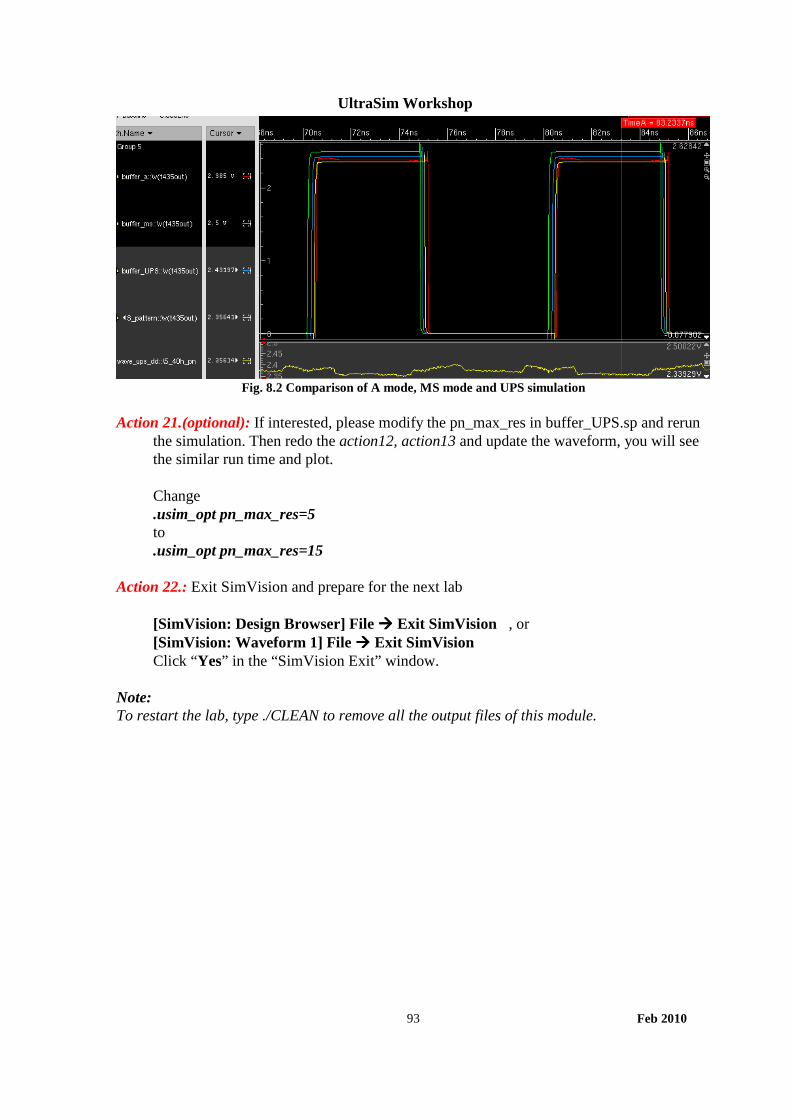
UltraSim Workshop
Feb 2010 93
Fig. 8.2 Comparison of A mode, MS mode and UPS simulation
Action 21.(optional): If interested, please modify the pn_max_res in buffer_UPS.sp and rerun
the simulation. Then redo the action12, action13 and update the waveform, you will see the similar run time and plot.
Change .usim_opt pn_max_res=5 to .usim_opt pn_max_res=15
Action 22.: Exit SimVision and prepare for the next lab
[SimVision: Design Browser] File ���� Exit SimVision , or [SimVision: Waveform 1] File ���� Exit SimVision Click “Yes” in the “SimVision Exit” window.
Note: To restart the lab, type ./CLEAN to remove all the output files of this module.

UltraSim Workshop
Feb 2010 94
9 DC leakage analysis The following dynamic and static circuit features are designed to help designers to find DC leakage paths or floating nodes. Dynamic DC Path Check This feature of UltraSim intends to help designers to find any DC leakage paths. All reported DC conduction paths are written into a file with the extension .pcheck. To qualify as a conduction path, each segment in the path must carry at least the threshold current specified by the parameter ith. There are 2 basic usages of DC leakage path checking. They are: Syntax .pcheck title_name dcpath <ith=threshold_current> <tth=time_duration> <node=[node1 node2...]> <inst=[inst1 inst2]> <xinst=[xinst1 xinst2]> <period=period_time|delay=delay_time> <time_window=[start1 stop1 start2 stop2 ...]> .pcheck title_name dcpath <ith=threshold_current> <tth=time_duration> <node=[node1, node2...]> <inst=[inst1 inst2]> <xinst=[xinst1 xinst2]> <at=[time1 time2...]> Floating Gate Induced Leakage Current Check This Ultrasim feature detects leakage paths between power supplies caused by floating nodes. First, Ultrasim detects Hi-Z nodes and forces their associated fanout transistors to be turned on . Second, it detects conducting paths between voltage source/ground nodes through the transistor with leakage currents larger than the threshold value ith . The conducting paths are written into a file with extension .pcheck. The usage of Floating Gate Induced Leakage Current Checking: Syntax .pcheck title floatdcpath <ith=threshold_current> <node=[node1, node2...]> <inst=[inst1 inst2]> <xinst=[xinst1 xinst2]> time_window=[time1 time2...] period=time5 at=[time6 time7...]
UltraSim Workshop
Feb 2010 95
Static High Impedance Node Check Ultrasim is able to check high impedance nodes without DC or transient simulation. A node is in high-impedance state if there is no possible conducting path between the node and any voltage sources specified in the netlist. The high impedance nodes are written into a file with the extension .rpt_hznode. The usage of ‘Static High Impedance Node Check’ is: Syntax .usim_report chk_hznode title <vnth=volt> <vpth=volt> <fanout=value> <pwl_time=time> <num=n> Static DC Path Check Ultrasim is able to detect DC paths between voltage sources without running DC or transient simulation. The DC path can consist of MOSFETs, BJTs, diodes, inductors, and resistors (<100Mohm). All other elements are treated as open. The elements in the DC path are written into a file with the extension .rpt_dcpath. The usage of ‘Static DC Path Check’ is: Syntax .usim_report chk_dcpath title <vnth=volt> <vpth=volt> <pwl_time=time> <num=n> <rpt_path=0|1> Now let us exam the usage of checks mentioned above. Simulating the 128K EEPROM case
This is a 128Kbit serial EEPROM circuit. X1 is the digital block and X2 is the memory array, address decoder, sense amp and charge pump. Since there may be too many DC paths in X2, we will only check DC paths in X1.
Action 1: Change to DC path check case folder
% cd modules/dc_path Action 2: Look at the pcheck statement in top.1 which is included by top.sp
%more top.1 First, you will find: .usim_restart file=top@save_2.050000e-06 .usim_opt sim_mode=df

UltraSim Workshop
Feb 2010 96
This is because the whole simulation will take more than 10mins. In order to shorten the simulation time, we used the save and restart feature to save the time. We know that the DC leakage will occur after 2.05uS. For the simulation, we will use DF mode.
Note: There are 7 simulation modes (S, A, MX, MS, DA, DF, DX) for selection. The default is MS mode. Speed can be set between 1-8, the default is 5). Second, you will see 3 pcheck statements: .pcheck dccheck1 dcpath ith=10u tth=10n inst=[x1] node=[vdd 0] time_window=[2.05u 2.07u] .pcheck dccheck2 dcpath ith=10u inst=[x1] at=[2.06u 2.07u] .pcheck cfloat2 floatdcpath ith=10u inst=[x2] at=[2.06u] The first one is to check each DC current path between vdd and gnd in subckt X1 starts from 2.05us and stops at 2.07us. The dc current path is reported in the file top.pcheck if the dc path current exceeds 10 uA and lasts longer than 10ns when checked. The second one is to check each DC current path in subckt X1 at 2.06us or at 2.07us. The DC current path is reported if the dc path current exceeds the default value of 10uA at 2.06us or at 2.07us.
Note: A voltage source node is a node that is directly connected to a voltage source (including, but not limited to, DC, PWL, SINE, PULSE voltage source). The ground node is also a voltage source node. Nodes connected to current sources are not qualified. Nodes connected to HDL/C models, and drivers defined in VEC or VCD files are not qualified either. If no nodes are specified, or none of the specified nodes qualifies, the simulator checks for DC paths between all voltage sources
Action 3: Check the warning_limit option in the top.1. Except .usim_opt and .pcheck, you will
also see:
.usim_report warning_limit=3 warning_id=[SFE-30]
.usim_report warning_limit=5 warning_id=[USIMMOD-7051] UltraSim provides some options to help the user manage the warning messages and make circuit debugging more efficient. “warning_limit” can be set in 2 option cards: .usim_opt or .usim_report. If appears in .usim_opt card, it is a global option that controls the maximum number for all warnings. However, there are times when the user may want to see some specific types of warning or warnings versus other warning or warnings. In this case, setting warning_limit with the .usim_report can prove to be useful. Thus, in this lab, as shown above, we will see only 3 warnings with ID of SFE-30 but 5 warnings with ID USIMMOD-7051 in the log file. Please note SFE here means the warnings are from parser while USIM means the warnings are from the kernel.

UltraSim Workshop
Feb 2010 97
Action 4: Run the simulation
% ultrasim +log top.out top.sp or % ./run
Action 5: Open top.out about warning messages. Please check if you can see only 3 warnings with ID as either SFE-30, but you will see 5 warnings with ID USIMMOD-7051. Action 6: Open top.pcheck
From the report, you will see the complete dc path. For “at” time points check, it will use default of tth=5. Only if the exceeded currents happen at or before the time point and last more than tth then they will be printed.
%more top.pcheck
****** Errors in Power Checks ***** Total of 4 error(s) found. Time is in nanoseconds. Title Error Count ---------------------------------------- cfloat2 (statistics are summarized at the end of file) dccheck1 (statistics are summarized at the end of file) dccheck2 (statistics are summarized at the end of file) ---------------------------------------- DC PATH POWER CHECK ERRORS: title ith(A) tth(ns) from(ns) to(ns) .pcheck dccheck1 dcpath node=[vdd 0] inst=[x1] ith=1.000e-05 tth=1.000e-08 time_window=[2.050e-06
2.070e-06] ------------------------------------------------------------------- dccheck1 1e-05 10 2054.52 2070 -------------------------------------------------------------------Path Begins Path 1: Connected nodes: vdd to: 0 Path Elements x1.xleak.x1i27.mp1i117 x1.xleak.x1i86.mn1i2 x1.xleak.x1i82.mn1i86 …
Action 7: Look at the static Hi-Z node check statement in top.1 % more top.1 You will find:

UltraSim Workshop
Feb 2010 98
.usim_report chk_hznode HiZ vnth=0.7 vpth=-0.7 fanout=1 pwl_time=2u It is to check high impedance nodes connected to MOSFET's gate. Note: The following rules are evaluation criteria of possible conducting path. MOSFET and JFET of n-type are considered on if Vg-Vs >= Vnth MOSFET and JFET of p-type are considered on if Vs-Vg >= -Vpth BJT, diode, resistor, and voltage sources are always considered on. Capacitor and current sources are always assumed to be off Action 8: Open top.rpt_hznode From the report, you will see all the high impedance nodes which connect to MOSFET’s gate only. % more top.rpt_hznode .TITLE 'This file is :./top.rpt_hznode' Static High Impedance Node Report For hiz Report nodes connected to MOSFET's gate only test_inb (test_inb) x1.n2 (serial_g.n2) x1.x1i571.n1n157 (serial_g.dffper.n1n157) x1.xleak.n1n43 (serial_g.dffpr.n1n43) x1.xleak.n1n60 (serial_g.dffpr.n1n60) x1.xspi.nwprot_sr (serial_g.spi_g.nwprot_sr) x1.xspi.x2i489.n1n157 (serial_g.spi_g.dlatrx.n1n157) x1.xtm_oscmx.n1n124 (serial_g.tmoscmxh.n1n124) x1.xtm_oscmx.n1n158 (serial_g.tmoscmxh.n1n158) x1.xtm_oscmx.n1n166 (serial_g.tmoscmxh.n1n166) Total reported nodes = 10
Action 9: Look at the static dcpath check statement in top.1 % more top.1 You will find: .usim_report chk_dcpath DCPath vnth=0.7 vpth=-0.7 pwl_time=2u rpt_path=1 It is to check all the DC paths between voltage sources. Note:

UltraSim Workshop
Feb 2010 99
The following rules are evaluation criteria of possible conducting path. MOSFET and JFET of n-type are considered on if Vg-Vs >= Vnth MOSFET and JFET of p-type are considered on if Vs-Vg >= -Vpth BJT is considered on if Vbe is forward biased by more than 0.5V. Diode is cinsidered on when forward biased by more than 0.5V. Action 10: Open top.rpt_dcpath From the report, you will see all the DC paths between Vdd and ground. % more top.rpt_dcpath .TITLE 'This file is :./top.rpt_dcpath' Static Leakage Path Report For dcpath Leakage Path From vdd (3.00V) to 0 (0.00V) Element Between Node And Node vdd vdd x2.x1i26.x4.mim11 vdd x2.blhv x2.x1i26.x4.mim17 x2.blhv x2.x1i26.x4.blhv1 x2.x1i26.x4.d1 x2.x1i26.x4.blhv1 0 End Path
Note: To restart the lab, type ./CLEAN to remove all the output files.

UltraSim Workshop
Feb 2010 100
10 Static ERC Checks
The static ERC check allows you to detect the following electrical design rule violations without running any simulation:
• MOSFET power switch whose bulk is not hard-wired to power supply. • MOSFET with forward biased junction. • MOSFET with bulk not hard-wired to power supply. • Unconnected MSOFET gate. • Unconnected MOSFET bulk. • Dangling node. • MOSFET in high VDD domain driven by MOSFETs in low VDD domain. • MOSFET in low VDD domain driven by MOSFETs in high VDD domain. • MOSFET directly shorting VDD and GND. • MOSFETs with gate connected directly to power supply. • top level input nodes not protected by ESD diodes.
It generates a report file (***.rpt_erc) listing the details of the violations based on the specified arguments. The spice syntax of ERC check is:
.usim_report erc title <powergatebulk=1> <underbiasbulk=1> <hotwell=1> <floatgate=1|2|3|4> <floatbulk=1|2> <dangle=1|2> <low2highvdd=1> <high2lowvdd=1> <powershort=1> <vhth=volt> <vlth=volt> <rmax=res> <pwl_time=time>
Action 1: Change to ERC check case folder
% cd modules/erc Action 2: Look for the following line in the file in top.sp
%more top.sp .usim_report erc ERcheck hotwell=1 floatgate=2 floatbulk=1 dangle=1 powershot=1 low2highvdd=1 vhth=2.0 vlth=1.0 pwl_time=2u num=10 .usim_report erc ERcheck2 gate2power=1 inputdiode=1 The followings are the meaning of the various arguments:
• erc: Key word to enable ERC check. • ERcheck: Title of the report. • hotwell=1: Reports MOSFET with bulk not connected to VDD or GND. • floatgate=2 : Reports unconnected MOSFET gate excluding top level nodes.

UltraSim Workshop
Feb 2010 101
• floatbulk=1: Reports all unconnected MOSFET bulk. • dangle=1: Reports all dangling nodes. • powershot=1: Reports MOSFETs with channel connected directly between VDD
and GND. • low2highvdd=1: Reports MOSFETs in high VDD domain driven by MOSFETs in
low VDD domain. • vhth=2.0: Any voltages above 2.0V are considered as VDD. • vlth=1.0: Any voltages below 1.0V are considered as GND. • pwl_time=2u: If specified, pwl sources are considered same as dc source. The
voltage level at 2us is used. • num=10: The first 10 warning messages in each type are printed. • Gate2power=1: Reports MOSFETs with gate connected directly to power supply. • Inputediode=1: Reports top level input nodes not protected by ESD diodes.
Action 3: Run the simulation
% ultrasim +log top.out top.sp or % ./run
Action 4: Open top.rpt_erc From the report, you will see all the detected violations. % more top.rpt_erc .TITLE 'This file is :./top.rpt_erc' ------------------------------------------------------------------- ERC - Node Dangle Error Report wpb_pin x2.x1i181.x7.n1n305 x2.x1i181.x7.n1n445 x2.x1i26.x3.n2n1057 x3.nc1 x3.nc2 x6.nc1 x6.nc2 x7.nc1 x7.nc2 Total reported nodes = 10 Only the first 10 nodes are reported here. There are more errornous nodes. -------------------------------------------------------------------

UltraSim Workshop
Feb 2010 102
ERC - Hotwell Error Report Element Name Bulk Terminal x2.x1i181.x9.x0.mpm1 blhv x2.x1i181.x9.x1.mpm1 blhv x2.x1i181.x9.x1.mpm11 blhv x2.x1i181.x9.x1.mpm12 blhv x2.x1i181.x9.x1.mpm2 blhv x2.x1i181.x9.x1.mpm20 blhv x2.x1i181.x9.x1.mpm21 blhv x2.x1i181.x9.x10.mpm1 blhv x2.x1i181.x9.x11.mpm1 blhv x2.x1i181.x9.x11.mpm11 blhv Total reported elements = 10 Only the first 10 elements are reported here. There are more errornous elements. ------------------------------------------------------------------- ERC - Float Gate Error Report (exclude top level nodes) Element Name Gate Terminal x2.x1i26.x3.mnm24 n2n1057 Total reported elements = 1 ------------------------------------------------------------------- ERC - Float Bulk Error Report (exclude top level nodes) Element Name Bulk Terminal x3.mnesd2 nc2 x3.mpesd1 nc1 x6.mnesd2 nc2 x6.mpesd1 nc1 x7.mnesd2 nc2 x7.mpesd1 nc1 x8.mnesd2 nc2 x8.mpesd1 nc1 Total reported elements = 8 ------------------------------------------------------------------- ERC - Cross Power Domain Error Report Low Vdd Driving High Vdd Domain Element Name Low Voltage Low Voltage Node High Voltage High Voltage Node x3.x1i104.mn1i2 1.80V vdd18 3.00V vdd x3.x1i104.mp1i1 1.80V vdd18 3.00V vdd x6.x1i104.mn1i2 1.80V vdd18 3.00V vdd x6.x1i104.mp1i1 1.80V vdd18 3.00V vdd x7.x1i104.mn1i2 1.80V vdd18 3.00V vdd x7.x1i104.mp1i1 1.80V vdd18 3.00V vdd

UltraSim Workshop
Feb 2010 103
x8.x1i104.mn1i2 1.80V vdd18 3.00V vdd x8.x1i104.mp1i1 1.80V vdd18 3.00V vdd Total reported elements = 8 ------------------------------------------------------------------- ERC - Cross Power Domain Error Report Low Vss Driving High Vss Domain Element Name Low Voltage Low Voltage Node High Voltage High Voltage Node Total reported elements = 0 ------------------------------------------------------------------- ERC - Gate Connected to Power Error Report: ercheck2 Element Name Gate Terminal Power x3.mnesd2 0 0.00V x3.mnesd4 0 0.00V x4.mnm3 0 0.00V x4.mp1i178 0 0.00V x4.mp1i182 0 0.00V x4.mp1i199 0 0.00V x4.mp1i203 0 0.00V x4.mp1i207 0 0.00V x4.mpm2 0 0.00V x6.mnesd2 0 0.00V Total reported elements = 10 Only the first 10 elements are reported here. There are more errornous elements. ------------------------------------------------------------------- ERC - Antenna Diode Check Error Report: ercheck2 Node Name Missing Diode Power esd_in ground Total reported nodes = 1 Reverse connected protecting diodes: d_esd_dio Total reported elements = 1

UltraSim Workshop
Feb 2010 104
11 Timing Analysis UltraSim allows you to perform timing analysis on specific nodes through a set of commands starting with .usim_ta. This example demonstrates the following timing checks: • Pulse Width Check reports nodes with pulse width outside a specific range. • Setup Check reports nodes with setup timing error relative to a reference node. • Hold Check reports nodes with hold timing error relative to a reference node. The circuit is a 16K bit SRAM which has 1024x16 bits of memory cells, 10-bit address input (A<9:0>), 16-bit data input (DI<15:0>), 16-bit data output (DO<15:0>), pre-charge input (PRE) and write/read control (WR, 1=write, 0=read). 11.1 Simulating the 16K bit SRAM
Action 1: Change to the sram16k_ta directory.
% cd modules/sram16k_ta
Action 2: Look at the top level netlist file, sram16k_ta.sp. % more sram16k_ta.sp The input stimuli are provided by the digital vector file sram16k_ta.vec. Near the end of the file are several timing analysis commands. We shall first simulate the circuit and view the waveforms. Then we will walk through each of the timing analysis commands. UltraSim Option: sim_mode=df speed=3 Note: There are 7 simulation modes (S, A, MX, MS, DA, DF, DX) for selection. The default is MS mode. Speed can be set between 1-8, the default is 5).
Action 3: Run UltraSim simulation.
% ultrasim +log sram16k_ta.out sram16k_ta.sp or % ./run
Action 4: View the sram16k_ta.veclog and sram16k_ta.vecerr files. Note that there are mismatch errors on the output signal DO<12>, DO<11>, DO<4>, DO<3>, DO<1>, DO<0> at time=1000ns. We created these errors intentionally by using a very narrow PRE pulse at time=1000ns.
Note:

UltraSim Workshop
Feb 2010 105
Search in the run directory for waveform files named sram16k_ta.vecexp and sram16k_ta.vecerr. By them, UltraSim provides a new way to view the expected vectors and vector errors in graphic besides opening the error file in text editor. This feature will be very helpful to see the difference between the simulation results and expected outputs in VEC/VCD/EVCD files.
Checking waveform with SimVision
Action 1: Start the waveform viewer.
% simvision& Action 2: Open waveform database using a previously saved command script.
[SimVision: Design Browser] File � Source Command Script…
Action 3: In the “Select SimVision Command File” window, select file sram16k_ta.sv and click Open. You can now inspect the waveforms of all the top level signals. Notice the very narrow PRE pulse at time=1000ns. At the last there is the v(vec_err) to display the vector error in graphic. If it stays at 0 it means there is no violation for the vectors check. However in this case, note there is a pulse at the time of 1000ns. This indicates there is at least one vector check fails. To get more details, it is able to check error on each bit by plotting signals in sram16k_ta.vecerr. Keep the waveform window open for further examination.
Fig. 11.1 Output of sram16k_ta.sp
11.2 Pulse Width Check Action 1: Open the file sram16k_ta.sp and find the following statements near the end of the
file:
.usim_ta PRE_MIN_WIDTH pulsew node=PRE tmin_low=10n tmax_low=1 tmin_high=10n tmax_high=1 .usim_ta DO_MIN_WIDTH pulsew node=DO<*> tmin_low=1n tmax_low=800n tmin_high=1n tmax_high=800n .usim_opt vl=2.5 vh=2.5

UltraSim Workshop
Feb 2010 106
These statements invoke the Pulse Width Check function. The syntax is .usim_ta title pulsew node=node1 tmin_low=min_low_time tmax_low=max_low_time tmin_high=min_high_time tmax_high=max_high_time <vl = logic_0_threshold> <vh =logic_1_threshold> <depth = value> <subckt = name> <start=time1> <stop=time2> This command is used to report pulse width errors on the waveforms of the specified nodes, A pulse width error occurs when the pulse width falls outside the range (min_low_time, max_low_time) for the logic 0 state, or the range (min_high_time, max_high_time) for the logic 1 state. The threshold values of the logic 0 and logic 1 states can be specified in the same command card. If they are not specified, the default values can be set up using the command .usim_opt vl=value vh=value. Please refer to UltraSim User Guide for more options on using this command. In this example, we set up UltraSim to report any pulse on the PRE signal narrower than 10ns or wider than 1s (equivalent to don’t care) and to report glitches on DO<15> ~ DO<0> wider than 800ns. The default threshold values for logic 0 and 1 are set to 2.5V. UltraSim reports all the timing errors in the output file sram16k_ta.ta.
Action 2: Open the output file sram16k_ta.ta. Review the reported pulse width violations and compare with the waveforms.
11.3 Setup Check Action 1: Look for the following statements near the end of the file sram16k_ta.sp:
.usim_ta AD_SETUP_TIME setup node=A<*> edge=both ref_node=PRE ref_edge=fall setup_time=5n .usim_ta DI_SETUP_TIME setup node=DI<*> edge=both ref_node=PRE ref_edge=fall setup_time=5n These statements invoke the Setup Check function. The syntax is .usim_ta title setup node=node1 edge=rise|fall|both ref_node=node2 ref_edge=rise|fall|both setup_time=time [window = window_size] [vl = logic_0_threshold] [vh = logic_1_threshold] [vrl = logic_0_threshold] [vrh = logic_1_threshold] [depth = value] [subckt = name] [start=time1] [stop=time2] This command is used to report setup timing errors on the specified nodes (node1) with respect to a reference node (node2). A setup timing error has occurred if a signal transition occurs between the times t_ref – setup_time and t_ref, where t_ref is the time when a reference transition occurs. The argument edge and ref_edge can be set to rise, fall , or both, which determine the permissible transitions on the signals and reference to

UltraSim Workshop
Feb 2010 107
trigger the checking. Please refer to UltraSim User Guide for more options on using this command. In this example, we set up UltraSim to report any setup timing violations on the signals A<9:0> and DI<15:0>. The minimum set up time is 5ns. Only a fall transition of the PRE signal will trigger the checking. UltraSim reports all the timing errors in the output file sram16k_ta.ta.
Action 2: Open the output file sram16k_ta.ta. Review the reported setup timing violations and
compare with the waveforms. 11.4 Hold Check Action 1: Look for the following statements near the end of the file sram16k_ta.sp:
.usim_ta AD_HOLD_TIME hold node=A<*> edge=both ref_node=PRE ref_edge=rise hold_time=5n .usim_ta DI_HOLD_TIME hold node=DI<*> edge=both ref_node=PRE ref_edge=rise hold_time=5n These statements invoke the Hold Check function. The syntax is .usim_ta title hold node=node1 edge=rise|fall|both ref_node=node2 ref_edge=rise|fall|both hold_time=time <window = window_size> <vl = logic_0_threshold> <vh = logic_1_threshold> <vrl = logic_0_threshold> <vrh = logic_1_threshold> <depth = value> <subckt = name> <start=time1> <stop=time2> This command is used to report hold timing errors on the specified nodes (node1) with respect to a reference node (node2). A hold timing error has occurred if a signal transition occurs between the times t_ref and t_ref + hold_time, where t_ref is the time when a reference transition occurs. The argument edge and ref_edge can be set to rise, fall , or both, which determine the permissible transitions on the signals and reference to trigger the checking. Please refer to UltraSim User Guide for more options on using this command. In this example, we set up UltraSim to report any hold time violation on the signals A<9:0> and DI<15:0>. The minimum hold time is 5ns. Only a rise transition of the PRE signal will trigger the checking. UltraSim reports all the timing errors in the output file sram16k_ta.ta.
Action 2: Open the output file sram16k_ta.ta. Review the reported hold time violations and
compare with the waveforms. Action 3: Exit SimVision.

UltraSim Workshop
Feb 2010 108
[SimVision: Design Browser] File � Exit SimVision , or [SimVision: Waveform 1] File � Exit SimVision Click “Yes” in the “SimVision Exit” window.
Note: To restart the lab, type ./CLEAN to remove all the output files.
12 Simulating Voltage Regulators (Voltage Regulator Option) Due to the continuous reduction of supply voltage and the adoption of multiple supply voltages within a chip, more and more mixed signal/RF or digital circuits use on-chip voltage regulators to generate internal supply voltages. All fast-SPICE simulators depend on efficient partitioning to achieve simulation speed up, which is possible only when the circuits are driven by ideal power supply. Using conventional partition technology, all the blocks connected to an internal regulated supply have to be contained in a single partition, resulting in unacceptable simulation performance. A novel simulation/partition technology, known as the Voltage Regulator (VR) option, has been developed for UltraSim to simulate designs with large circuit blocks powered by internal voltage regulators. 12.1 Simulating a 16-bit multiplier powered by an internal voltage regulator Action 1: Change to the mult16_vr directory.
% cd modules/mult16_vr Action 2: Look at the top-level netlist file, mult16_vr.sp.
% more mult16_vr.sp
The top level netlist contains a 16 bit digital multiplier (mult16x16), a voltage regulator (vreg), and a PWL voltage source (VH). By peeking into the two low level netlists (mult16.net and vreg.net), you can observe that the multiplier is powered by a global supply node (vdd), which is generated by the voltage regulator. The latter obtains its supply from the PWL voltage source.
Now pay attention to the simulation options. The digital block is simulated with the local options sim_mode=df (Digital Fast), whereas the analog voltage regulator is simulated with the option sim_mode=a (Analog). The use of these sim_mode options should be obvious. The Ultrasim VR partition/simulation technology is invoked by the following command:
.usim_vr inst=X0 node=vdd The argument inst=X0 specifies the instance of the voltage regulator block. (Similar to other ultrasim options, either instance or subcircuit name can be specified.) Multiple voltage regulators can be specified. In particular, all the circuit blocks that contribute to

UltraSim Workshop
Feb 2010 109
the generation of the regulated supply voltages should be specified by multiple block arguments. The node=vdd argument specifies the internal power supply node driven by the voltage regulator. Multiple regulated supply nodes can be specified.

UltraSim Workshop
Feb 2010 110
Note: There are 7 simulation modes (S, A, MX, MS, DA, DF, DX) for selection. The default is MS mode. Speed can be set between 1-8, the default is 5).
Action 3: Run UltraSim simulation and wait till the simulation completes.
%ultrasim +log mult16_vr.out mult16_vr.sp Action 4: (Optional) To appreciate the speed up provided by the VR option, you may want to
comment out the usim_vr command and re-run the simulation. To preserve the simulated results from last run., you may re-name the top level netlist before re-running it.
%cp mult16_vr.sp mult16_no_vr.sp (Comment out the usim_vr command.) %ultrasim +log mult16_no_vr.out mult16_no_vr.sp
Checking waveform with SimVision Action 1: Start the waveform viewer.
%simvision &
The SimVision Design Browser window appears.
Action 2: Open waveform database using a previously saved command script. [SimVision: Design Browser] File ���� Source Command Script

UltraSim Workshop
Feb 2010 111
Action 3: In the “Select SimVision Command Script” window, select file vr.sv and click Open. Inspect the waveform of the regulated supply voltage (vdd). You should also see the input and output waveforms of the mutiplier displayed in the digital format.
Fig. 12.1 VR
Action 4: After viewing the results, you can now exit SimVision and go on to read the next
case.
[SimVision: Design Browser] File ���� Exit , or [SimVision: Waveform 1] File ���� Exit Click “Yes” in the “SimVision Exit” window.
Note: To restart the lab, type ./CLEAN to remove all the output files.

UltraSim Workshop
Feb 2010 112
13 Multithreading Simulation The new UltraSim S and A mode in MMSIM11.1 support full multithreaded simulation, including the parallelization of the device model evaluation, and matrix solving. The multithreading delivers a performance gain of up to 2x on 4 cores, and up to 4x on 8 cores when using single threaded simulation as reference. A maximum number of 16 cores is supported. All used cores need to be on the same machine. Distributed simulation isn’t supported. The multithreading isn’t expected to degrade any accuracy when comparing against single thread simulation. The multithreaded version of MX mode may also provide value for selected mixed signal designs when comparing against MS mode. By default multithreading is disabled in S A and MX mode. It can be enabled:
a) on command line with +mt (UltraSim detects the optimal number of cores)
+mt=”number of threads”, i.e. +mt=8 b) or as UltraSim option in the netlist .usim_opt mt=”number of threads”, i.e. .usim_opt mt=4
Simulating Parallel A Mode Action 1: Change to the mult16_vr directory.
% cd modules/mult16_vr Action 2: Look at the file usim_a.sp.
% more usim_a.sp
Option “sim_mode=a” is set.
Action 3: Run Ultrasim simulation and wait till the simulation completes.
% ultrasim +log usim_a.out usim_a.sp
With 2.83G CPU on Linux, the simulation time is about 6min30sec.
Action 4: Create new netlist file usim_a_4t.sp for parallel A simulation.
% cp usim_a.sp usim_a_4t.sp
Open usim_a_4t.sp and uncomment out ‘usim_opt mt=4’. .usim_opt mt=4

UltraSim Workshop
Feb 2010 113
Action 5: Run Ultrasim simulation with parallel A mode. Before starting the simulation, you should make sure that the server has more than 4 CPUs.
% ultrasim +log usim_a_4t.out usim_a_4t.sp With 2.83G CPU on Linux, the runtime is about 3min6sec. Runtime is speedup about
2X with 4 thread simulation.
Note: To restart the lab, type ./CLEAN to remove all the output files.
14 Static Power Grid Calculator The static power grid calculator can be used to calculate all pin-to-tap or pin-to-subnode resistances based on the net description from a DSPF or SPEF file (a pre-layout netlist file is not required). The analysis is performed statically, no transient simulation is needed, so it can be done very quickly even for full chip analysis. The analysis assumes that all pins of the same net are shortened. The output of this calculator is a list of instance terminals, a.k.a taps and their effective resistances to the pins. The design in this lab is a small sample and hold cell of an ADC circuit. We will examine the usage of the static power grid calculator by checking the effective resistances of all the relevant devices’ terminals to VSS net. Action 1: Change to SPRES directory
%cd SPRES Action 2: Let us exam the command file % more spres.config The comments in this file explain the purpose of each command in this file. Action 3: Run ultrasim % ultrasim -r spres.config Action 4: Let us exam the three output files one by one: StaticRes.ulog, res-VSS.rout and res-VSS.nr10minr0.01.report % more StaticRes.ulog This file contains the information about the simulation, for example, total number of resistor for the analyzed net, total number of nodes… etc. % more res-VSS.rout

UltraSim Workshop
Feb 2010 114
This file contains a list of the tap nodes with its effective resistance from the pin. Please note hname is the instance name while name is the tap node name. % more res-VSS.nr10minr0.01.report This file is generated due to “report” command in the spres.config file. This file contains of the list of the tap node names that has the top 10 largest effective resistances. Note: To restart the lab, type ./CLEAN to remove all the output files.

UltraSim Workshop
Feb 2010 115
15 Electro-Migration and IR-Drop analysis
Netlist based EMIR analysis Ultrasim netlist based EM/IR flow packages Electro-Migration (EM) and IR drop analysis capabilities within Ultrasim simulator. It is independent of extraction tools. By exploiting UltraSim hierarchical stitching technique, it provides much needed capacity in EM and IR analyses for large designs, such as mixed signal designs and memory circuits. The flow not only provides textual EM and IR reports, but also visually displays EM and IR results as color-coded violation maps. It is seamlessly integrated with the Cadence Virtuoso environment. Overlaying the violation maps on top of the original layout is easily managed. Furthermore, the flow provides cross probing between the textual output and the visual display, very convenient for debugging. This workshop covers
1) Run Ultrasim simulation from batch mode. Parasitics are stitched, and back-
annotated. This step will create 5 intermediate files:
input.emir0_bin input_phys.data input_phys.layer input_phys.field input_phys.name
input.emir_bin contains the voltage/current information, while the other four files contain all the geometry information embedded in the dspf/spef file originally.
2) Post-process the simulation results and the geometry information. Both textual
reports and graphic display will be examined. The design is a small S/H block in a large ADC design. This workshop is based on OA database. Please keep in mind USIM netlist based EMIR flow works on CDBA too.

UltraSim Workshop
Feb 2010 116
The file structure for EMIR is as follows: -------------------------------------------------------------------------- ./ |-- setup.csh # setup environment script |-- reset_all.csh # clean script |-- cds.lib # lib definition file |-- display.drf # display control file |-- emDataFile.txt # em rule file |-- LOCAL_LIBS # lib directory | `-- AMSBC # AMSBC lib |-- schematic # schematic directory | |-- adc_sample_hold.dspf # dspf file | |-- control.txt # emir control file | |-- input.scs # spectre netlist | |-- runUltrasim # run ultrasim script | |-- control_new.txt # emir control file for new advanced flow | |-- input_new.scs # spectre netlist for new advanced flow | `-- runUltrasim_new # run ultrasim script for new advanced flow `-- share # PDK lib
15.1 Running UltraSim Simulation Action 1: Set up environment. % cd EMIR then % source setup.csh You will see the following: Report software versions ========================================================================= @(#)$CDS: virtuoso version 6.1.5 07/19/2011 04:50 (sjfdl053) $ sub-version IC6.1.5.500.5 ========================================================================= @(#)$CDS: ultrasim version 11.1.0 32bit 07/14/2011 03:33 (usimamd64-47) $ sub-version 11.1.0.157 =========================================================================
UltraSim Workshop
Feb 2010 117
The file reset_all.csh is for cleaning the directory from previously created files. Note that you must have sourced the setup.csh file in the UltraSim_Workshop directory at the beginning of this document. Action 2: at the x-terminal prompt, issue the following command % cd schematic
Action 3: Let us look at the netlist. The schematic netlist is called input.scs. The corresponding parasitic file is adc_sample_hold.dspf. The parasitic file is stitched to the schematic netlist. Please open File input.scs with any text editor and go down to the bottom, you will see that options are grouped for easy understanding, as shown below. ================== input.scs ==================
*-----------------------------------------------------------------* * USIM options: sim mode and speed * *-----------------------------------------------------------------* .usim_opt sim_mode=a speed=4 *-----------------------------------------------------------------* * USIM Stitching options * *-----------------------------------------------------------------* .usim_opt spf="i1 ./adc_sample_hold.dspf" .usim_opt spfxtorprefix="MI I" .usim_opt spfskippwnet=off *-------------------------------------------------------------------* * Command to invoke USIM Netlist Based Flow * *-------------------------------------------------------------------* .usim_emir format=[layout] =============================================
As the name suggests, the simulation itself is netlist based, i.e., command line driven. Action 4: Run the simulation by issuing command % ./runUltrasim Action 5: Examine the files that are created. % cd psf % ls You will see

UltraSim Workshop
Feb 2010 118
input.dsn input.spfrpt input.emir0_bin input_phys.data input_phys.field input_phys.index input_phys.layer input_phys.name input_phys.spfsdb input.trn logFile input.ulog Let’s go into the log file input.ulog to check the stitching statistics. --------------------------------------------------------------------------------------- Nets | parsed 18| expanded 18| not expanded 0 Capacitors| parsed 3709| expanded 37 09 Resistors | parsed 6803| expanded 6 803 New nodes | added 5950| | --------------------------------------------------------------------------------------- nets stitched with C-only 0 nets stitched with RC 18 --------------------------------------------------------------------------------------- Please note the file input.spfrpt contains all the stitching information, which will help you to debug the stitching process of the simulation. Now we are ready for post processing. If the new advanced EMIR flow below is not of interest, please go to Section 12.2. *Optional: New Advanced EMIR flow The new advanced EMIR flow has significant improvement in capacity compared to the previous flow. It targets huge block and full chip EMIR analysis. In the new flow, two simulations are needed and Ultrasim has to be invoked twice manually. The first simulation dumps out a file with suffix *.emirtap.sp. The second one is running ultrasim with this *.emirtap.sp file. The way of post-processing is the same as previous flow. After the second simulations finished, a *.emirtap.emir0_bin file will be generated. Please use this *.emirtap.emir0_bin file as the binary database. Optional 1: Set up environment % source setup.csh Report software versions ========================================================================= @(#)$CDS: virtuoso version 6.1.5 07/19/2011 04:50 (sjfdl053) $

UltraSim Workshop
Feb 2010 119
sub-version IC6.1.5.500.5 ========================================================================= @(#)$CDS: ultrasim version 11.1.0 32bit 07/14/2011 03:33 (usimamd64-47) $ sub-version 11.1.0.157 ========================================================================= Optional 2: Change directory % cd schematic Optional 3: Let us look at the netlist for new advanced flow. The schematic netlist is called input_new.scs. Please open File input_new.scs and go down to the bottom, you will see that options as shown below. There are a few differences from previous flow, the option: .usim_emir type = power nets=[i1.VDD i1.VSS] “power” is one of the two key words for new flow, the other keyword is signal, Currently [signal | power] cannot work simultaneously. If you want to do both analyses in the design, please separate them. ================== input_new.scs ==================
*-----------------------------------------------------------------* * USIM options: sim mode and speed * *-----------------------------------------------------------------* .usim_opt sim_mode=a speed=4 *-----------------------------------------------------------------* * USIM Stitching options * *-----------------------------------------------------------------* .usim_opt spf="i1 ./adc_sample_hold.dspf" .usim_opt spfxtorprefix="MI I" *-------------------------------------------------------------------* * Command to invoke USIM Netlist Based Flow * *-------------------------------------------------------------------* .usim_emir type=power nets=[i1.VDD i1.VSS] ================================================== Optional 4: Run the simulation by issuing command % ./runUltrasim_new

UltraSim Workshop
Feb 2010 120
The binary file input_new.emirtap.emir0_bin is generated in directory ./schematic/psf when simulation finished.
15.2 Post-Processing for EM and IR analysis In this section, we will study
a) The control file that specifies the conversion to OA. b) Convert the binary database to OA database. c) Examine the textual EM and IR report. d) Examine graphical display of the IR analysis. d) Examine graphical display of the EM analysis.
Convert the intermediate binary database to OA database. Action 6: open File control.txt in ./schematic directory with any textual editor (For new flow, control file is control_new.txt) This file controls the conversion to OA database. ================== control.txt ================== color level = 8 layout format = [oa] pwnet net=[i1.vdd] analysis=[vmax iavg] + net=[i1.vss] analysis=[vmax iavg] signal net=[i1.*] analysis = [iavg] emdata file= ../emDataFile.txt report text=1 warnmsg limit=10000000 EMIR-2 ============================================= Action 7: check the file emDataFile.txt ================== emDataFile.txt ================== cadGrid = 0.005 routingLayers = ("Poly" "Metal1" "Metal2" "Metal3" "Metal4" "Metal5" "Metal6" "Metal7" "Metal8" "Metal9") viaLayers = ("Cont" "Nimp" "Pimp" "Via1" "Via2" "Vi a3" "Via4" "Via5" "Via6" "Via7" "Via8") viaWidthList = (("Nimp" 0.26) ("Pimp" 0.26) ("Cont" 0.238) ("Via1" 0.28) ("Via2" 0.28) ("Via3" 0.2) ("Via4" 0.2) ("Via4" 0.2)) xrefLayers = ( ( "sti" ("Nimp" "Nimp")) ( "sti" ("Pimp" "Pimp")) ...... avgCurrentDensSpecList = (

UltraSim Workshop
Feb 2010 121
(nil layer "Poly" minW 0.0 maxW -1.0 currentDensi ty ((2.0 , 110))) (nil layer "Metal1" minW 0.0 maxW -1.0 currentDensi ty ((2.0 , 110))) …… ================================================= The EM data input file needs to be created to specify technology information, such as current density limits, and mapping between the layers. The current density limits can be expression in length, width, simulation temperature, via_range … etc. Length based rules are supported. Action 8: go to $USIM_EMIR_FLOW directory and invoke virtuoso % cd $USIM_EMIR_FLOW % virtuoso &
Action 9: click Tools-> library Manager, Open the layout:
Library: AMSBC Cell: adc_sample_hold_emir View: layout
You could see the layout for adc_sample_hold block.
Action 10: click Launch->Netlist-Based EMIR, you should see a new menu button Netlist-Based EMIR show up in the menu bar.

UltraSim Workshop
Feb 2010 122
Action 11: click Netlist-Based EMIR, you will see the following pull down menu (Fig. 15.1).
Fig. 15.1 pull down menu
Action 12: Click Generate EMIR Violation Map . Then in the pop-up window, type in the full path for Files input.emir0_bin and control.txt . You can use the Browse buttons too (look under schematic/ and psf/). Then type in a view name, say, new_emir, for the to-be-generated violation map. Click Generate Violation Map button (Fig.15.2). (For new flow, please use input_new.emirtap.emir0_bin as EMIR binary file, and control_new.txt as control file)

UltraSim Workshop
Feb 2010 123
Fig. 15.2 Generate Violation Map
An Info window as the one to the left pops up (Fig.15.3). Close the Info window and OK the Generate EMIR Violation map window.
Fig.15.3 pops up info window
Now the OA database, textual IR, and EM reports are all generated. Let us examine the textual output first. Action13: % cd $USIM_EMIR_FLOW/schematic/psf % ls You will see input.dsn input.emir0_bin input_phys.data input_phys.field input_phys.index input_phys.layer input_phys.name input_phys.spfsdb input.rpt_em

UltraSim Workshop
Feb 2010 124
input.rpt_ir input.trn logFile input.ulog input.spfrpt There are two newly created files input.rpt_em and input.rpt_ir . Action 14: Examine EM textual report, which is $USIM_EMIR_FLOW/schematic/psf/input.rpt_em. For each node set in your control file, all violations records in the text file, such as: ----------------------- NET "i1.vdd" -------------- ----------------- avg There is no resistor whose current density exceeds the limit. %failed resistor layer current width pathLength density limit needed width/ #vias X1 Y1 X2 Y2 (A) (um) (um) (A/um) (A /um) (um/#) (um) (um) (um) (um) pass-10.07% rr1027 Via2 1.612m 4.480 15 5.735 359.725u 400.000u 15(16) 60.190 206.060 60.190 206.060 pass-26.00% rr1026 Via2 331.518u 1.120 155 .735 295.998u 400.000u 3(4) 60.200 199.280 60.200 199.280 pass-31.61% rr1019 Via2 1.226m 4.480 15 5.735 273.553u 400.000u 11(16) 90.040 206.110 90.040 206.110
.... ------------------------------------------------ In this table, each resistor’s name, layer, current density and coordinates (X1, Y1, X2, Y2) are given. %failed column gives the violation state. Please note a) pathLength is specifically the total length used in length based rules. b) needed width/#vias are the needed width a metal resistor must be widened to pass EM
check. Needed # of vias are the needed number of vias if a via resistor is to pass the EM check.
Action 15: Examine IR textual report, which is $USIM_EMIR_FLOW/schematic/psf/input.rpt_ir. In this text file, voltage-drop, netname, time, layer and coordinate X, Y, are displayed as below: -------------------- "i1.vdd" PIN ----------------- ------------------ max VOLTAGE-DROP NETNAME TIME LAY ER X Y (V) (s) (um ) (um) 7.181m MPM1@16:s 614.148p mwires 75.120 76.080 7.181m MPM3@9:s 614.148p Cont 75.120 76.080 7.180m VDD:567 614.148p Metal1 75.120 95.840 7.180m VDD:566 614.148p Metal1 75.120 90.640 .... ----------------------------------------------------------------

UltraSim Workshop
Feb 2010 125
Now let us continue to the graphic display portion of EM and IR analysis.
15.3 IR analysis Action 16: In the layout window, click Netlist-Based EMIR-> IR Analysis. An IR Analysis Setup form like below shows up (Fig.15.4). OK the Setup form.
Fig.15.4 setup IR analysis
An IR Analysis form as below shows up (Fig.15.5):
Fig.15.5 IR Analysis Window
USIM netlist based EMIR flow allows user to
Text Window
Cross probing
Navigate pins
Color bins
Choose Tap, Internal and All

UltraSim Workshop
Feb 2010 126
1) Choose different pins to analyze. 2) The IR drop voltages are color coded according to its IR drop value and binned. The
user can specify the number of colors in both control file and here in this form. 3) The displayed nodes are grouped into Tap nodes and internal nodes, the user can choose
to display either Tap node or internal nodes or both. Tap node is the device terminals, internal node is connection between RC net.
4) Sorting and searching capabilities are provided. 5) Zoom to Node can cross probe between the violation map and the text subwindow. 6) The violation maps can be displayed standalone or overlaid on top of the original
layout. Action 17: click Browse. A Select Pins window as the one to the left pops up, Select i1.vss, and OK the form (Fig.15.6).
Fig.15.6 select pins
Action 18: in the IR Analysis form, click the red arrow right next to Tap, Select All, then check the buttons to the left of all the bins (y0, y1 …. y7). You should see a window like below (Fig.15.7).

UltraSim Workshop
Feb 2010 127
Fig.15.7 selects All Action 19: Try each button on the right side:
� Save Violation Map to View: allows you to save the violation map for the specified pins in a view.
� Search: allows you to search in the form text window by node name. � Refresh Text Window: refreshes the content in the form text window. � Refresh EMIR Map: refreshed EMIR Map display in layout window. � Select Presistors in A window: allows you to select a region in the layout window. To
select presistors in a layout window: Display the violation map in the layout window, click Select Presistors in a Window, and then select the desired area in the layout window by drawing a box in the window. The parasitic resistors located in the text subwindow are highlighted in the report.
� Zoom to Node: allows you to cross probe between the text report and the violation map. To perform this task, select a node in the form text window and click Zoom to Node. A magnified view of all resistors connected to the node is displayed in the layout window.
� turn on or off certain layers. Action 20: The textual sub-window can be sorted by IR drop value, node name and type of nodes. Click on related top name such as “Voltage Drop”, “ Node Name” “ Node” to sort them.

UltraSim Workshop
Feb 2010 128
The color-coded violation map can be displayed standalone or overlay on top of original layout. The buttons “Toggle Visibility of Violation Map” and “Toggle visibility of Reference view” are serving this purpose. Action 21: Click Toggle Visibility of Reference View, notice that the original layout disappears in the layout window and you should see a window like below (Fig.15.8).
Fig.15.8 Toggle Visibility of Violation Map
This is the peak IR drop violation map for i1.vss net. To help the designers debugging EM and IR problems, cross-probing capabilities are provided.

UltraSim Workshop
Feb 2010 129
Action 22: Click Toggle Visibility of Refernce view and then click Select Presistors in a Window, and then select the desired area in the layout window by drawing a box in the window. The parasitic resistors located in the text subwindow are highlighted in the report.
Fig.15.9 Select Presistors in a Window
Action 23: Click Search button, a Search Node Name window pops up, type in VSS:17 and OK the form (Fig.15.10).
Fig.15.10 Search Node Name
Notice all nodes that match “VSS:17” are high-lighted in the text window. Use the scroll bar to see all.

UltraSim Workshop
Feb 2010 130
Action 24: click Zoom to Node button, layout is zoomed to the selected nodes. Note: all the resistors that are connected to these nodes are displayed (Fig.15.11).
Fig.15.11 Zoom to Node USIM EMIR also allows the user to see the full chip IR drop violation map, which includes all the nets for which IR drop analysis are requested. The button Show Full Chip Violation Map is for this purpose.
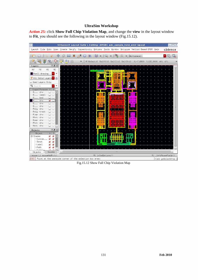
UltraSim Workshop
Feb 2010 131
Action 25: click Show Full Chip Violation Map, and change the view in the layout window to Fit , you should see the following in the layout window (Fig.15.12).
Fig.15.12 Show Full Chip Violation Map

UltraSim Workshop
Feb 2010 132
Action 26: Click Toggle Visibility of Reference View, observe the violation map and the original layout are overlaid on top of each other (Fig.15.13).
Fig.15.13 Toggle Visibility of Reference View This concludes the IR analysis. Action 27: Close IR Analysis form. Next, we will work on EM analysis.
14.4 EM Analysis Action 28: In the layout window, click Netlist-Based EMIR, then EM Analysis, an EM Analysis Setup form pops up, this form is similar to the IR Analysis Setup form. OK the form. You should see a window like below (Fig.15.14).
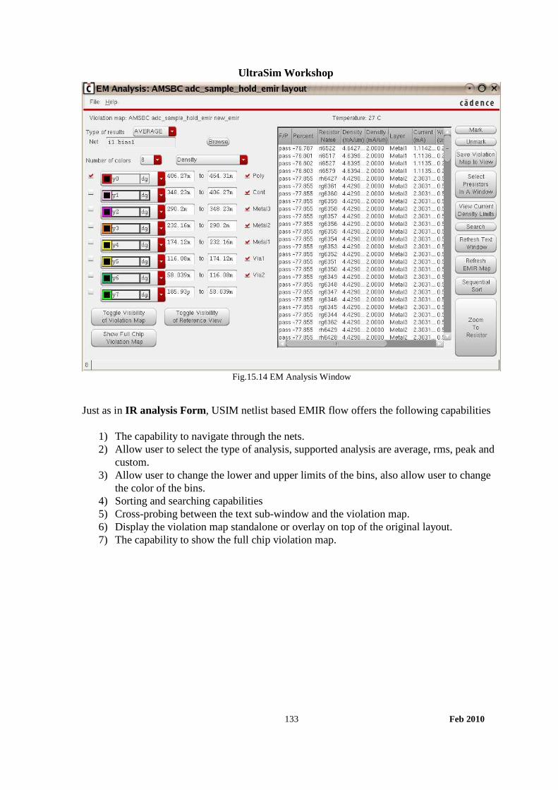
UltraSim Workshop
Feb 2010 133
Fig.15.14 EM Analysis Window
Just as in IR analysis Form, USIM netlist based EMIR flow offers the following capabilities
1) The capability to navigate through the nets. 2) Allow user to select the type of analysis, supported analysis are average, rms, peak and
custom. 3) Allow user to change the lower and upper limits of the bins, also allow user to change
the color of the bins. 4) Sorting and searching capabilities 5) Cross-probing between the text sub-window and the violation map. 6) Display the violation map standalone or overlay on top of the original layout. 7) The capability to show the full chip violation map.

UltraSim Workshop
Feb 2010 134
Action 29: check on the boxes left of all the bins. Use Browse to select i1.vdd to analysis. Then click Refresh Text Window (Fig.15.15) .
Fig. 15.15 Refresh Text Window Each column, in the text sub-window, is sortable by simply clicking the title of the column. Action30: Try each buttons on the right side
� Mark: places a number (#) sign in front of the selected resistor in the text report. � Unmark: removes the number (#) sign from the selected resistor in the text report. � Save Violation Map to View: allows you to save the violation map for the specified
pins in a view. � Select Presistors In A Window: allows you to select a region in the layout window. To
select presistors in a layout window: Display the violation map in the layout window, click Select Presistors in a Window, and then select the desired area in the layout window by drawing a box in the window. The parasitic resistors located in the text subwindow are highlighted in the report.
� View Current Density Limits: allows you to view the EM data file. � Search: allows you to search in the form text window by resistor name. � Refresh Text Window: refreshes the content in the form text window. � Refresh EMIR Map: refreshed EMIR Map display in layout window. � Sequential Sort: allows you to multi-sort in the text window.

UltraSim Workshop
Feb 2010 135
� Zoom To Resistor: allows you to cross probe between the text report and the violation map. To perform this task, select a resistor in the form text window and click Zoom to Resistor. A magnified view of all resistors connected to the resistor is displayed in the layout window.
Action 31: Click Toggle Visibility of Reference View, you should see below (Fig.15.16).
Fig.15.16 Toggle Visibility of Reference View
This is the violation map of average current density for i1.vdd.

UltraSim Workshop
Feb 2010 136
Action 32: click Toggle Visibility of Reference View; observe the original layout is overlaid, as shown below (Fig.15.17).
Fig.15.17 Toggle Visibility of Reference View with overlaid original layout
Action 33: click Search, and a Select Resistor Name window as the one to the left pops up. Type in ri622 and OK the form (Fig 14.18).
Fig.15.18 Search Resistor Name

UltraSim Workshop
Feb 2010 137
Notice Resistor ri622 is highlighted in the text sub-window, as shown below (Fig.15.19).
Fig.15.19 highlighted Resistor ri622

UltraSim Workshop
Feb 2010 138
Action 34: click Zoom to Resistor; observe the layout is zoomed to this resistor. (Highlighted yellow olor in Fig.15.20)
Fig.15.20 Zoom to Resistor

UltraSim Workshop
Feb 2010 139
Action 35: USIM netlist based EMIR flow also allows user to select an area in the layout, such that the corresponding resistors in that area are highlighted in the text window (Fig 15.21). change the view of the layout window to Fit first, if necessary, Click Togggle visibility of Violation map to make sure the whole violation map is in view. then Click Select Presistor in A Window , then select an area in the layout window by simply left clicking the mouse and dragging the mouse pointer. The resistors that reside within this window will be highlighted. See an example below
Fig15.21 highlighted resistors that selected in layout
If you cannot see any highlighted resistors, please scroll down the scroll bar.

UltraSim Workshop
Feb 2010 140
Action 36: Click View Current Density Limits , this will show the EM rules as below (Fig.15.22).
Fig.15.22 Display EMData File
Examine the em rule data. Close the Display EMData File window.
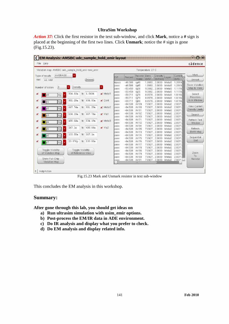
UltraSim Workshop
Feb 2010 141
Action 37: Click the first resistor in the text sub-window, and click Mark , notice a # sign is placed at the beginning of the first two lines. Click Unmark ; notice the # sign is gone (Fig.15.23).
Fig.15.23 Mark and Unmark resistor in text sub-window
This concludes the EM analysis in this workshop.
Summary:
After gone through this lab, you should get ideas on a) Run ultrasim simulation with usim_emir options. b) Post-process the EM/IR data in ADE environment. c) Do IR analysis and display what you prefer to check. d) Do EM analysis and display related info.

UltraSim Workshop
Feb 2010 142
16 Case Studies 16.1 Case Study: Using the UltraSim Save and Restart features
The UltraSim save (.usim_save) and restart (.usim_restart) features allow you to start a simulation, stop at a pre-defined breakpoint, save a snapshot of the simulation database, and end the simulation. You can restart the simulation based on the saved state.
Action 1: Change to modules/case-study/dram1gb directory, and then create a new input file,
% cd modules/case_study/dram1gb % cp dram1gb.sp dram1gb_save.sp
Action 2: Edit the newly created file. Uncomment the following line near the end of the file: .usim_save file=dram1gb@save time=1u This statement will invoke the save option. The file=save_file argument specifies the name of the file to save the simulation state. The time=save_time argument specifies the time at which the operating point is saved. Multiple save_time can be specified, and each time point will generate a saved file with unique name.
Action 3: Run UltraSim simulation. % ultrasim +log dram1gb_save.out dram1gb_save.sp
Action4: Now view the current directory and you will discover that UltraSim has generated a new file “dram1gb@[email protected]” which contains the internal state of the 1Gb DRAM. Notice how fast UltraSim can generate the file even for such a large design.
Action 5: To demonstrate the restart feature, create another new input file.
% cp dram1gb.sp dram1gb_restart.sp
Action 6: Edit the newly created file. Uncomment the following line near the end of the file: .usim_restart file=dram1gb@[email protected] This statement will invoke the restart option. The file=save_file argument specifies the name of the file that contains the saved simulation state.

UltraSim Workshop
Feb 2010 143
Action 7: Run UltraSim simulation and wait till the simulation completes. From the log on screen, you will find the simulation starts from 1us.
% ultrasim +log dram1gb_restart.out dram1gb_restart.sp
Checking waveform with SimVision Action 1: Open waveform database a previously saved command script. [SimVision: Design Browser] File ���� Source Command Script… Action 2: In the “Select SimVision Command Script” window, select file dram1gb_restart.sv
and click Open. You should see the results from both simulations. Obviously, the new simulation started at 1us.
Fig.16.1 Output of dram1Gb.sp started from 1us
Action 3: After viewing the waveforms, close the SimVision window.
[SimVision: Design Browser] File ���� Exit Simvision , or [SimVision: Waveform 1] File ���� Exit Simvision Click “Yes” in the “SimVision Exit” window.
Note: To restart the lab, type ./CLEAN to remove all the output files.

UltraSim Workshop
Feb 2010 144
16.2 Case study: Bisection optimization In this lab, a basic D Flip-Flop circuit is used to demonstrate how to use Bisection feature of UltraSim to optimize the design parameter. The bisection methodology seeks the optimal value of a specified input parameter associated with a goal value of an output variable, using the binary search strategy. It is usually used in timing optimization, such as searching optimized data setup time, or hold time before clock signal. In the process of bisection search, Ultrasim does the following steps. 1) Perform transient simulation with the specified parameter set at the lower and upper limits respectively. The measurement results for the two limits must be that one accomplishes the goal and the other fails. Otherwise, Ultrasim stops and prints a message. 2) Perform the simulation at the mid-point of the searching range and compares the measurement with the goal value. The searching range is halved by choosing new searching range being either the first half or the second half based on the measurement result. 3) Perform step 2 iteratively until the following conditions are met: the relative tolerance on the input variable and output variable is satisfied, or the maximum number of iteration is reached. Use Model To start the bisection search, 4 statements are used to define the optimization model, parameters need optimization, measurement goal, and analysis. � .MODEL defines the optimization method (BISECTION) and the criteria to stop the
iteration, the maximum number of iteration and relative tolerances.
.MODEL OptModelName OPT METHOD=BISECTION <RELIN =value> <RELOUT =value> <ITROPT =value>
� .PARAM defines the parameters need optimization (input variable) and its initial value,
lower limit value, and upper limit value.
.PARAM ParamName = OPTxxx(<Initial>, <Lower>, <Upper>)
UltraSim Workshop
Feb 2010 145
Note: Bisection method allows only one parameter and ignores the initial value.
� .MEASURE defines the measurement of the output variable and its goal value, which is
used to evaluate the fitness of a parameter value, i.e., if the parameter value is accepted or not.
.MEASURE TRAN MeasTitle <MeasFuncs> GOAL = GoalValue
� .TRAN statement defines the bisection and optimization method.
.TRAN <TranStep> <TranEndTime> SWEEP OPTIMIZE =OptParFun RESULTS=MeasTitle MODEL =OptModeName FASTSWEEP=ON/OFF
Next, user can follow the steps to utilize bisection search feature to find out the best delay time for a simple D Flip-Flop circuit. It has two input signals: data and CLK. Assume they have a transition (0�1) at Td and Tclk. We know the data should be stable for a while (setup time) before CLK switches. That is, the transitions need to satisfy the following condition:
Tclk > Td + setup_time In this situation, an output transition (0�1) on output Q will occur. Otherwise, no transition is found and the Q remains “0”. We can simply set measurement MAX to detect the transition. If the measurement result is “1”, there is a transition; if “0”, no transition occurs. By bisection analysis, we can find a value of setup_time that “just” makes a transition at the output. Simulating the D Flip-Flop
Action 1: Change to DFF directory.
% cd modules/case_study/DFF
Action 2: Look at the top level spice netlist. % more dff.sp Vclk CLK 0 pwl(0n 0 1n 0 1.1n vdd 3n vdd 3.1n 0 10n 0 10.1n vdd) Vdata data 0 pwl(0n 0 5n 0 6n vdd td=delay) These defined clock and data signals. Please note the td=delay is the parameter needs optimization by using bisection search. .param delay=opt1(0n, 0n, 6n) .model optmod opt method=bisection .measure tran vout max v(Q) goal='0.9*vdd' .tran 0.1n 20n sweep optimize=opt1 results=vout model=optmod fastsweep=off

UltraSim Workshop
Feb 2010 146
Above statements are used to do bisection search. The goal is to have transition (0�1) on signal Q. The range for delay is from 0 to 6ns. .usim_opt sim_mode=ms In this example, since it is a basic digital circuit, default MS mode is selected. Note: There are 7 simulation modes (S, A, MX, MS, DA, DF, DX) for selection. The default is MS mode. Speed can be set between 1-8, the default is 5).
Action 3: Run UltraSim simulation and wait till the simulation completes.
%./run or % ultrasim +log dff.out dff.sp
After all the simulations are finished, check the dff.out and dff.optlog. % more dff.optlog You will see the following .title 'title:dff.optlog' ---------------------------------------------------------------------------- iter lower upper current result 1 0 6e-09 0 2.5 2 0 6e-09 6e-09 0.0113226 3 0 6e-09 3e-09 2.5 4 3e-09 6e-09 4.5e-09 0.0376893 5 3e-09 4.5e-09 3.75e-09 2.5 6 3.75e-09 4.5e-09 4.125e-09 2.5 7 4.125e-09 4.5e-09 4.3125e-09 2.5 8 4.3125e-09 4.5e-09 4.40625e-09 2.5 9 4.40625e-09 4.5e-09 4.45313e-09 2.5 10 4.45313e-09 4.5e-09 4.47656e-09 2.5 11 4.47656e-09 4.5e-09 4.48828e-09 2.5 12 4.48828e-09 4.5e-09 4.49414e-09 2.5 Optimization Method bisection Optimization Parameter delay Optimized Value 4.49414e-09
vout 2.5 Goal 2.25 There are 12 iterated runs to meet the requirement. In dff.out, it is seen in each run there are DB building and DC calculating procedures. In fact if there is no change of circuit among these iterations, it will speed up if only have one DB building and DC calculation

UltraSim Workshop
Feb 2010 147
procedure. Write down the simulation time which can be found at the bottom of the dff.out file. As reference, the simulation takes 12.6s in 2.8G CPU Linux box.
Action 4: Open dff.sp and change the fastsweep from “off” to “on”. Action 5: Run UltraSim simulation again
%./run or % ultrasim +log dff.fast.out dff.sp
Action 6: After all the simulations are finished, check the dff.out and dff.optlog again. Note the simulation takes less time. As reference, it takes 2.4s in 2.8G CPU Linux box. This means, it speeds up 5 times.
Action 7 : Open the dff.mea0 and check the setup time. It is measured from the middle point of switch in data signal to the middle point of switch in clk signal. If interested, user can check the waveform of data, clk and Q in simvision. A simvision config file called dff.sv is provided. Note: To restart the lab, type ./CLEAN to remove all the output files.
UltraSim Workshop
Feb 2010 148
16.3 Case study: HCI & NBTI Reliability analysis This is the demo for UltraSim’s reliability analysis. This tool models the effect of aging on the circuit’s performance. We look at two aging mechanisms: Hot Carrier Injection (HCI), this comes into play in devices, PMOS and NMOS with short channel widths, typically below 130nm; the second, Negative Bias Temperature Instability (NBTI), usually affects PMOS transistors with thin gate insulators (< 50 A). In both cases, during circuit operation, carriers and traps end up in the gate insulator, in the interface between the insulator and the oxide, in the depletion regions, etc. The change in circuit performance due to these effects is also dependent on the circuit activity, so this type of analysis has to be coupled with a transient simulation for accurate results.
Simulating the ring oscillator circuit
Action 1: Change to ring oscillator directory. % cd modules/case_study/osc13
Action 2: Look at the BSIM4 nmos model deck, AgeNMOS.mod. % more model/AgeNMOS.mod This is a standard BSIM4 model deck that has been enhanced with aging parameters. As you look at the top of the deck, you will see the standard BSIM4, level 54, model parameters. However, if you scroll down to the bottom of the deck, you’ll see the additional aging parameters. Note that these parameters have been commented out with “*relxpert: “. You can use this deck with any Spice type simulator and it will work fine, but when UltraSim reads it, and reliability analysis is enabled, the simulator uses these parameters to model the aging of the device. These parameter model the change of the standard BSIM4 model parameters over time. For example, note that there are 5 parameters (under the “AgeMos model parameters” section) that begin with the letter ‘h’ models the change of BSIM4 parameter ‘vth0’ over time due to HCI effects. Similarly, there are 5 parameters that model ‘vth0’s change due to NBTI effects. These new parameters are curve fitting parameters. The underlying equations are proprietary and not visible to the user. Note: These parameters were extracted using Virtuoso Device Modeling BSIM Pro Plus tool, available from ProPlus Design Solutions Inc..
Action 3: Look at the netlist for the ring oscillator circuit. % more osc13.sp

UltraSim Workshop
Feb 2010 149
At the top, there is an ultrasim options card: .usim_opt sim_mode=ms tol=0.025 This means that we will be simulating in ‘Mixed Signal’ mode and the simulator tolerance (same as reltol in Spectre) will be set to 0.025. Note: There are 7 simulation modes (S, A, MX, MS, DA, DF, DX) for choosing. The default is MS mode Speed can be set between 1-8, the default is 5) A few lines down we see the following lines *relxpert: .age 10y *relxpert: .deltad 0.05 *relxpert: .agemethod agemos These lines invoke the reliability analysis. They mean that we will perform a simulation with the devices aged 0 years and 10 years. Then UltraSim will calculate the lifetime of each transistor, where the criterion for lifetime is the point where the idsat of the device changes by 5%, and we will use the AGEMOS parameters in the model deck to determine the aging effects. The .MEASURE statement in the netlist measures the period of the oscillating output. This is what we will be checking to see if the design’s performance has changed unacceptably over the 10 years.
Action 4: Run the analysis.
% ultrasim +log osc13.out osc13.sp
You will be running two transient analysis, one for new devices (time=0) and the other for aged ones (time=10 years). The reliability analysis takes the transient simulation to be a model of the steady state activity of the design that has been running for 10 years.
Examining the simulation result Action 1: After the simulation is complete, look at the reliability reports.
% more osc13.ba0
This file has 4 columns. The first is a list of all devices that had significant degradation in the aging process. The second column is the amount of aging in the forward mode of transistor operation. The third, the amount of aging in reverse mode and the fourth column is the total amount of aging. The term ‘aging’ here quantifies the dynamic stress applied to each devices This age number is a mathematical quantity. You can call it stress. It is not the time in the .age card. This measure takes into account changes in Vgs, Vds, Vbs and the channel’s electric field. The aging report should be used in a relative manner.

UltraSim Workshop
Feb 2010 150
% more osc13.bo0
This is the lifetime report. Again, 4 columns. This reliability report is very interesting. The first column lists all devices that had significant degradation in the aging process. The second is the total ‘aging’ (taken from the report in file osc13.ba0). The third column is the amount of degradation of the idsat of the device and the fourth is a calculation of the lifetime of the device before the idsat degrades by 5% (because we set *relxpert: .deltad 0.05) in the netlist. Here we have real reliability problems with the following devices:
xi2.mp xi7.mp xi1.mp xil1.mp xi10.mp xi8.mp xil2.mp xi3.mp xi9.mp xil3.mp xil7.mp xi11.mp xi5.mp xi6.mp xi12.mp xil4.mp xi4.mp xi0.mp xil5.mp xil6.mp
The lifetime for all of them is less than 0.0006 year. As the circuit is in operation, these devices will suffer Idsat degradation very quickly. The transistor lifetime is different than the circuit operation lifetime. This report can be used to debug any reliability issues in the design. The designer needs to decide if the circuit operation after 10 year is acceptable versus his specification. For solving HCI issues, he can increase the length of the devices. For solving NBTI issue, he can reduce the supply voltage. You can select to study only HCI degradation effects by adding the command card: *relxpert: .hci_only You can select to study only NBTI degradation effects by adding the command card: *relxpert: .nbti_only By default, UltraSim provides the degradation of both HCI and NBTI if the models support both reliability parameters.
Action 2: Look at the measurement of the period of the oscillator using new devices.
% more osc13.meas0 Action 3: Look at the measurement of the period of the oscillator that has been aged 10 years.
% more osc13_age1.meas0
Note the change between the two measurements. It should be more than a 10% difference. We now have a way to quantify potential reliability problems with designs before we go to fabrication and possibly run into either yield problems or excessive

UltraSim Workshop
Feb 2010 151
‘burn-in’ failure rates. It also eliminates the need to ‘over-design’ the part and the penalty in cost and performance.
Note: To restart the lab, type ./CLEAN to remove all the output files.
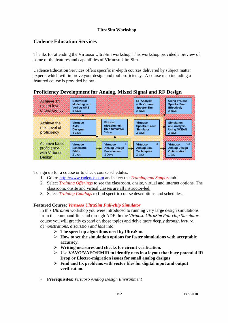
UltraSim Workshop
Feb 2010 152
Cadence Education Services Thanks for attending the Virtuoso UltraSim workshop. This workshop provided a preview of some of the features and capabilities of Virtuoso UltraSim. Cadence Education Services offers specific in-depth courses delivered by subject matter experts which will improve your design and tool proficiency. A course map including a featured course is provided below. Proficiency Development for Analog, Mixed Signal and RF Design
To sign up for a course or to check course schedules:
1. Go to: http://www.cadence.com and select the Training and Support tab. 2. Select Training Offerings to see the classroom, onsite, virtual and internet options. The
classroom, onsite and virtual classes are all instructor-led. 3. Select Training Catalogs to find specific course descriptions and schedules.
Featured Course: Virtuoso UltraSim Full-chip Simulator
In this UltraSim workshop you were introduced to running very large design simulations from the command-line and through ADE. In the Virtuoso UltraSim Full-chip Simulator course you will greatly expand on those topics and delve more deeply through lecture, demonstrations, discussion and labs into:
� The speed-up algorithms used by UltraSim. � How to set the simulation options for faster simulations with acceptable
accuracy. � Writing measures and checks for circuit verification. � Use VAVO/VAEO/EMIR to identify nets in a layout that have potential IR
Drop or Electro-migration issues for small analog designs � Find and fix problems with vector files for digital input and output
verification.
• Prerequisites: Virtuoso Analog Design Environment
Achieve basic proficiency with Virtuoso Design
Achieve an expert level of proficiency
Achieve the next level of proficiency
Virtuoso Schematic Editor 2 days
L Virtuoso Analog Design Environment 2 Days
L Virtuoso Analog Sim. Techniques 2 days
XL Virtuoso Analog Design Optimization 1 day
GXL
Virtuoso AMS Designer 3 days
Virtuoso UltraSim Full-Chip Simulator 3 days
Virtuoso Spectre Circuit Simulator 2 days
Simulation and Analysis Using OCEAN 2 days
Behavioral Modeling with Verilog-AMS 3 days
RF Analysis with Virtuoso Spectre Sim. 2 days
Using Vrtuoso Spectre Sim. Effectively 2 days