Ultrahigh hydrogen-sorbing palladium metallic-glass ...
7
This journal is © The Royal Society of Chemistry 2019 Mater. Horiz., 2019, 6, 1481--1487 | 1481 Cite this: Mater. Horiz., 2019, 6, 1481 Ultrahigh hydrogen-sorbing palladium metallic-glass nanostructures† Baran Sarac, * a Yurii P. Ivanov, bc Tolga Karazehir, d Marlene Mu ¨ hlbacher, e Baris Kaynak, f A. Lindsay Greer, b A. Sezai Sarac g and Ju ¨ rgen Eckert ae Pd-Based amorphous alloys can be used for hydrogen energy- related applications owing to their excellent sorption capacities. In this study, the sorption behaviour of dc magnetron-sputtered and chronoamperometrically-saturated Pd–Si–Cu metallic-glass (MG) nanofilms is investigated by means of aberration-corrected high-resolution transmission electron microscopy (HRTEM), X-ray photoelectron spectroscopy, and electrochemical techniques. The volume expansion of DV = 10.09 Å 3 of a palladium hydride unit cell obtained from HRTEM images due to the hydrogenation of the Pd–MG nanofilms is 1.65 times larger than DV of the Pd-polycrystalline counterpart loaded under the same conditions. Determined by scanning transmission electron microscopy-high annular dark-field imaging and electron energy loss spectroscopy, the huge difference between the two Pd-based systems is accounted for by the ‘‘nano- bubbles’’ originating from hydrogenation, which generate active sites for the formation and expansion of spatially dispersed palladium hydride nanocrystals. A remarkable difference in the hydrogen sorption capacity is measured by electrochemical impedance spectroscopy compared to the Pd polycrystal nanofilms particularly in the a and b regions, where the maximum hydrogen to palladium ratio obtained from a combination of chronoamperometry and cyclic voltammetry is 1.56 and 0.61 for the MG and Pd-polycrystal nanofilms, respectively. The findings place Pd–MGs among suitable material candidates for future energy systems. As an abundant, clean and renewable energy source, hydrogen is evaluated as a new material for the replacement of the currently used fossil fuels. Compared to other hydrogen storage techniques, 1–3 metal hydrides have the capability of storing large amounts of hydrogen without the need for external pressure or heat. 4–6 Due to the absorption of hydrogen into the bulk layers of the metal, 7–9 current state-of-the-art metal hydrides have higher volumetric density and lower total storage energy (12.5% of the net calorific value of hydrogen 10 ) as compared to the hydrogen gas or liquid hydrogen. Moreover, compared to physisorption, metal hydride formation via electrochemical bonding is generally accepted to yield higher volumetric and gravimetric densities of hydrogen storage. 11 Palladium is one of the key materials currently used for hydrogen storage and catalysis with excellent kinetic reversibility at ambient temperatures. 12–14 However, the high cost of Pd in bulk a Erich Schmid Institute of Materials Science, Austrian Academy of Sciences, 8700 Leoben, Austria. E-mail: [email protected] b Department of Materials Science & Metallurgy, University of Cambridge, Cambridge CB3 0FS, UK c School of Natural Sciences, Far Eastern Federal University, 690950, Vladivostok, Russia d Department of Energy System Engineering, Adana Arparslan Tu ¨rkes Science and Technology University, 01250 Saricam, Adana, Turkey e Department of Materials Science, Chair of Materials Physics, Montanuniversita¨t Leoben, 8700 Leoben, Austria f Department Polymer Science, Montanuniversita ¨t Leoben, 8700 Leoben, Austria g Polymer Science and Engineering, Nanoscience & Nanoengineering, Istanbul Technical University, 34469 Istanbul, Turkey † Electronic supplementary information (ESI) available. See DOI: 10.1039/c9mh00316a Received 26th February 2019, Accepted 11th April 2019 DOI: 10.1039/c9mh00316a rsc.li/materials-horizons New concepts Advanced materials with efficient hydrogen interactions are expected to play a major role in future energy conversion and storage systems. Despite their limited hydrogen storage capability and high costs, Pd-based nanomaterials are currently used for hydrogen storage and catalysis because of their excellent kinetic reversibility. Among them, Pd-based metallic glasses (Pd–MGs) can be considered as more efficient candidates due to their grain-free amorphous nanostructure with extra interstitial sites for a higher amount of hydrogen sorption. This study comprises, for the first time, an in-depth study of the unique hydrogenation behaviour of Pd–MG nanofilms sputtered on a Si substrate via physical vapour deposi- tion. Aberration-corrected HRTEM and STEM-HAADF/-EELS techniques confirmed the lattice expansion of 10.09 Å 3 obtained from the FFT patterns, which corroborates the extensive sorption capacity of Pd-based MGs (around 1.65 times larger than that for its Pd-counterparts). Compared to the lattice expansion of the Pd polycrystal nanofilms with the same thickness (50 nm), the calculated maximum H/M = 1.56 is 2.55 times larger. The considered Pd–MG improves the overall hydrogen storage capability through the electrochemically-induced nanobubbles. The ground-breaking concept of this study is that we have remarkably enhanced the metal–hydrogen interaction and palladium hydride formation via a newly designed nanofilm (Pd 79 Si 16 Cu 5 ) and electrochemical hydrogenation. Materials Horizons COMMUNICATION Open Access Article. Published on 23 April 2019. Downloaded on 1/24/2022 12:51:08 PM. This article is licensed under a Creative Commons Attribution-NonCommercial 3.0 Unported Licence. View Article Online View Journal | View Issue
Transcript of Ultrahigh hydrogen-sorbing palladium metallic-glass ...
This journal is©The Royal Society of Chemistry 2019 Mater. Horiz., 2019, 6, 1481--1487 | 1481
Cite this:Mater. Horiz., 2019,
6, 1481
Ultrahigh hydrogen-sorbing palladiummetallic-glass nanostructures†
Baran Sarac, *a Yurii P. Ivanov, bc Tolga Karazehir, d Marlene Muhlbacher, e
Baris Kaynak,f A. Lindsay Greer, b A. Sezai Sarac g and Jurgen Eckert ae
Pd-Based amorphous alloys can be used for hydrogen energy-
related applications owing to their excellent sorption capacities.
In this study, the sorption behaviour of dc magnetron-sputtered
and chronoamperometrically-saturated Pd–Si–Cu metallic-glass
(MG) nanofilms is investigated by means of aberration-corrected
high-resolution transmission electron microscopy (HRTEM), X-ray
photoelectron spectroscopy, and electrochemical techniques. The
volume expansion of DV = 10.09 Å3 of a palladium hydride unit cell
obtained from HRTEM images due to the hydrogenation of the
Pd–MG nanofilms is 1.65 times larger than DV of the Pd-polycrystalline
counterpart loaded under the same conditions. Determined by
scanning transmission electron microscopy-high annular dark-field
imaging and electron energy loss spectroscopy, the huge difference
between the two Pd-based systems is accounted for by the ‘‘nano-
bubbles’’ originating from hydrogenation, which generate active
sites for the formation and expansion of spatially dispersed palladium
hydride nanocrystals. A remarkable difference in the hydrogen sorption
capacity is measured by electrochemical impedance spectroscopy
compared to the Pd polycrystal nanofilms particularly in the a and b
regions, where the maximum hydrogen to palladium ratio obtained
from a combination of chronoamperometry and cyclic voltammetry is
1.56 and 0.61 for the MG and Pd-polycrystal nanofilms, respectively.
The findings place Pd–MGs among suitable material candidates for
future energy systems.
As an abundant, clean and renewable energy source, hydrogenis evaluated as a new material for the replacement of thecurrently used fossil fuels. Compared to other hydrogen storagetechniques,1–3 metal hydrides have the capability of storing largeamounts of hydrogen without the need for external pressureor heat.4–6 Due to the absorption of hydrogen into the bulk layersof the metal,7–9 current state-of-the-art metal hydrides have highervolumetric density and lower total storage energy (12.5% of the netcalorific value of hydrogen10) as compared to the hydrogen gas orliquid hydrogen. Moreover, compared to physisorption, metalhydride formation via electrochemical bonding is generallyaccepted to yield higher volumetric and gravimetric densitiesof hydrogen storage.11
Palladium is one of the key materials currently used forhydrogen storage and catalysis with excellent kinetic reversibility atambient temperatures.12–14 However, the high cost of Pd in bulk
a Erich Schmid Institute of Materials Science, Austrian Academy of Sciences,
8700 Leoben, Austria. E-mail: [email protected] Department of Materials Science & Metallurgy, University of Cambridge,
Cambridge CB3 0FS, UKc School of Natural Sciences, Far Eastern Federal University,
690950, Vladivostok, Russiad Department of Energy System Engineering, Adana Arparslan Turkes Science and
Technology University, 01250 Saricam, Adana, Turkeye Department of Materials Science, Chair of Materials Physics,
Montanuniversitat Leoben, 8700 Leoben, Austriaf Department Polymer Science, Montanuniversitat Leoben, 8700 Leoben, Austriag Polymer Science and Engineering, Nanoscience & Nanoengineering,
Istanbul Technical University, 34469 Istanbul, Turkey
† Electronic supplementary information (ESI) available. See DOI: 10.1039/c9mh00316a
Received 26th February 2019,Accepted 11th April 2019
DOI: 10.1039/c9mh00316a
rsc.li/materials-horizons
New conceptsAdvanced materials with efficient hydrogen interactions are expected toplay a major role in future energy conversion and storage systems. Despitetheir limited hydrogen storage capability and high costs, Pd-basednanomaterials are currently used for hydrogen storage and catalysisbecause of their excellent kinetic reversibility. Among them, Pd-basedmetallic glasses (Pd–MGs) can be considered as more efficient candidatesdue to their grain-free amorphous nanostructure with extra interstitialsites for a higher amount of hydrogen sorption. This study comprises, forthe first time, an in-depth study of the unique hydrogenation behaviour ofPd–MG nanofilms sputtered on a Si substrate via physical vapour deposi-tion. Aberration-corrected HRTEM and STEM-HAADF/-EELS techniquesconfirmed the lattice expansion of 10.09 Å3 obtained from the FFTpatterns, which corroborates the extensive sorption capacity of Pd-basedMGs (around 1.65 times larger than that for its Pd-counterparts).Compared to the lattice expansion of the Pd polycrystal nanofilms withthe same thickness (50 nm), the calculated maximum H/M = 1.56 is2.55 times larger. The considered Pd–MG improves the overall hydrogenstorage capability through the electrochemically-induced nanobubbles.The ground-breaking concept of this study is that we have remarkablyenhanced the metal–hydrogen interaction and palladium hydride formation via
a newly designed nanofilm (Pd79Si16Cu5) and electrochemical hydrogenation.
MaterialsHorizons
COMMUNICATION
Ope
n A
cces
s A
rtic
le. P
ublis
hed
on 2
3 A
pril
2019
. Dow
nloa
ded
on 1
/24/
2022
12:
51:0
8 PM
. T
his
artic
le is
lice
nsed
und
er a
Cre
ativ
e C
omm
ons
Attr
ibut
ion-
Non
Com
mer
cial
3.0
Unp
orte
d L
icen
ce.
View Article OnlineView Journal | View Issue
1482 | Mater. Horiz., 2019, 6, 1481--1487 This journal is©The Royal Society of Chemistry 2019
and micro-scale size and its moderate affinity to oxidizing orreducing environments under extreme conditions create big barriersagainst energy-based industrial applications.12,15 Cu containingPdSi-based metallic-glass (MG) nanofilms can serve as a remedyto this problem by showing higher durability against severeenvironments due to their grain-free amorphous structure whilesignificantly decreasing the cost due to the substitution of Pd withSi and Cu.16 In our previous study, the electrosorption (adsorption,absorption, desorption, and evolution) behaviour of hydrogen andkinetic parameters such as charge transfer resistance, as well asthe double layer and adsorption capacitance were investigatedusing a combination of cyclic voltammetry and electroimpedancespectroscopy.17 Depending on the Cu content, PdSi-based metallicglass nanofilms can remarkably enhance metal–hydrogen inter-action and palladium hydride (PdHx) formation. Although thisphenomenon can be linked to the non-translational structuralmotifs on the nm scale and the free volume in Pd-based metallicglasses, which probably generates additional interstitial sites for ahigher amount of hydrogen sorption,18–20 the mechanism andextent of palladium hydride formation in these multicomponentamorphous nanofilms are still unclear.
Here, we utilized an aberration-corrected high-resolutiontransmission electron microscopy (HRTEM) technique with apoint-to-point resolution of less than 0.1 nm, which allowscharacterization of palladium hydride crystals with diametersof several nanometers. Composition and thickness analyses were
performed by high-angle annular dark-field imaging in scanningtransmission electron microscopy mode (HAADF-STEM) in orderto assess the chemical segregation within the Pd–Si–Cu nanofilmdue to electrochemical hydrogenation. A comparative study withunhydrogenated Pd–Si–Cu nanofilms, as well as a polycrystallinePd nanofilm of similar thickness, was performed to highlightthe extent of hydride formation in each case. The hydridesaccumulate around ‘‘nanobubbles’’ with diameters of up to 4 nm,which is discovered to be the main reason for the ultra-highamounts of hydrogen storage in PdSiCu metallic-glass nanofilms.
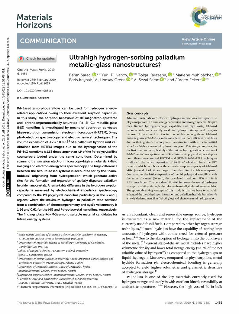
A typical dc magnetron-sputtered nanofilm on a silicon chipis shown in Fig. 1a. Grazing incidence X-ray diffraction (GIXRD)analysis shows a broad diffraction maximum for the Pd79Si16Cu5
nanofilm (Fig. 1b) as opposed to the sharp peaks obtained for thepolycrystalline Pd nanofilm (Fig. S1a – ESI†). The first peakmaximum of the Pd polycrystal (40.121) shifts to a larger 2y valuefor the MG sample (40.541) by the inclusion of Si and Cu. Similarto the literature findings, upon Cu addition, our previous XRDinvestigation showed a remarkable decrease in the interatomiclattice spacing (i.e. volumetric contraction) due to the smalleratomic radii of Cu. This results in broadening of the first sharppeak of the Pd sample, where this peak is strongly influenced bythe contributions of Pd–Si and Pd–Cu bonds.17 The first diffusepeak maximum of Pd84Si16 (2y = 40.281) shifts to 2y = 40.541 forthe 5 at% Cu addition (Pd79Si16Cu5). The more Pd is replacedwith Cu, the bigger the shift in 2y towards larger values.
Fig. 1 Synthesis and structural/surface characterization of a Pd79Si16Cu5 film. (a) Digital microscopy image of a PVD sputtered film on a Si substrate withcoating dimensions of 1.8 mm � 0.6 mm (scale bar 1 mm). (b) GIXRD analysis of the same film. Fitting of the first broad peak using the pseudo-Voigtfunction. (c) 3D profile analysis of a 2 � 2 mm region of a MG thin film performed via AFM. (d) Line scan (yellow dashed lines in c) of the AFM image; theroot mean square roughness is 0.66 nm. The line-scan roughness for the Pd polycrystalline sample is 0.29 nm. (e) Survey scan of the Pd–MGas-sputtered (unhydrogenated) and hydrogenated samples. The magnified view of the red area shows the Pd 3d3 and Pd 3d5 valence states. The blackdashed lines pass through the maxima points of the two valence states of the as-sputtered sample. A slight shift in the maxima of the hydrogenatedsample towards higher binding energies is observed (B0.2 eV).
Communication Materials Horizons
Ope
n A
cces
s A
rtic
le. P
ublis
hed
on 2
3 A
pril
2019
. Dow
nloa
ded
on 1
/24/
2022
12:
51:0
8 PM
. T
his
artic
le is
lice
nsed
und
er a
Cre
ativ
e C
omm
ons
Attr
ibut
ion-
Non
Com
mer
cial
3.0
Unp
orte
d L
icen
ce.
View Article Online
This journal is©The Royal Society of Chemistry 2019 Mater. Horiz., 2019, 6, 1481--1487 | 1483
The line scan profile obtained by atomic force microscopy(AFM) analysis in Fig. 1c shows a surface roughness of RRMS =0.66 nm (Fig. 1d). The root mean square roughness, RRMS,obtained from the scanned area is 0.64 and 3.37 nm for the Pd andMG thin films, respectively. PdSi-based metallic glasses with Cucontent were found to have higher surface roughness compared tothe PdSi–MGs without Cu. On the other hand, our previous findingsobtained from the electrochemical circuit modeling (ECM) showthat hydrogen absorption in Pd-based glassy thin films is mainlyindependent of this roughness factor.17 Compared to the inhomo-genously scattered bumps obtained from the 3D profile of PdTF asshown in Fig. S1b (ESI†), the MG shows a more homogenousdispersion of surface asperities. For the Palladium Thin Film (PdTF)and Metallic-Glass Thin Film (MGTF) samples, the correlated actualsurface areas obtained from the AFM measurements for the 4 mm2
projected area are 4.005 mm2 and 4.077 mm2, respectively. For thecyclic voltammetry of samples with such small roughnessvalues, the literature theoretically and experimentally provesthe independence of the electrode roughness in relation to theshape of the CV curves and peak currents.21
The X-ray Photoelectron Spectroscopy (XPS) study surveyscan (Fig. 1e) shows a small shift in the peak maxima of Pd3d3/2 and Pd 3d5/2 valence states towards higher binding energies(inset) upon electrochemical hydrogenation. Si 2p3, Cu 2p1/2, andCu 2p3/2 peaks do not shift after hydrogenation (as confirmed inour previous work).17 Thus, no chemical interaction between Siand H, and Cu and H has been detected after hydrogenation. Forthis reason, Pd is the main metal interacting with the sorbedhydrogen from the active sites of the MG sample. Fig. S2 (ESI†)shows the seamless attachment on the atomic-scale between theSi/SiO2 substrate and the MG nanofilm before hydrogenation.Fig. S3 (ESI†) shows an HRTEM image of a hydrogenated Pd thinfilm. It reveals the polycrystalline structure of Pd with an averagegrain size of 10–20 nm. The thickness of the polycrystalline layerwas measured to be B40 nm. Due to the high precision andstability of the employed PVD sputtering technique, the thicknessof the polycrystalline layer is constant across the sample.
To evaluate the saturation time and to determine the sorbedhydrogen in terms of the applied potential, we have performedcombinatorial chronoamperometry (Fig. S4 – ESI†) and cyclic
voltammetry (Fig. S5 – ESI†) tests using the MG sample. Athigher saturation potentials (from 0.4 V to 0.2 V vs. RHE) thesample readily reaches its hydrogen saturation limit within10 seconds. In comparison, B50 mm Pd foil in 1 M H2SO4
solution can be saturated in ca. 300 s.22 Such fast hydrogenationkinetics of this film is mainly due to its considerably smallthickness of 50 nm. While the hydrogen evolution reactionstarts below 0.15 V (inset), MG cannot fully store readily sorbedhydrogen. The release of excess hydrogen leads to an increase inthe current density.
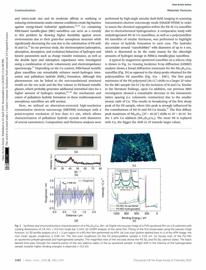
After chronoamperometric saturation, cyclic voltammogramsof the nanofilms were recorded. Fig. 2a shows the cathodic (navyblue) and anodic (green) scans of the Pd–MG nanofilm saturatedat 0.2 V. The changes in the shapes of the scans in the chargetransfer resistance, RCT, obtained from the equivalent circuitmodel of the EIS data were ascribed to phase transformations(see Fig. S6 – ESI†). A double-layer region is observed above0.28 V, corresponding mainly to the formation of a solid-solutionin the metal (the a phase). Between 0.28 V and 0.18 V, electro-chemically-bonded hydrogen starts to diffuse into the bulksample while more hydrogen attaches to the surface (the a + bphase). As the potential drops down, between 0.18 V and 0.04 V,absorption dominates due to the transfer of hydrogen ionsinto the bulk sample and their attachment to the active sites(the b phase). On the contrary, the desorption of hydrogenfrom these sites and the movement of hydrogen towards thesurface is observed in the anodic scan within the same region.With the sharp decrease in the current density, the electro-catalysis of hydrogen starts to take place below 0.04 V in thecathodic scan.
The ECM was further employed to model the impedancespectra of the MG and crystalline Pd nanofilms to investigatetheir capacitive response. In our previous study, the replacementof Pd with Cu by only 5% was proven to have a tremendousincrease in the double layer and adsorption capacitance of thePdSi-based MG thin films.17 The adsorption capacitance para-meter, Yad, calculated from the impedance values of the constantphase element (details given in the ESI† – Materials andmethods, Electrochemical measurements) is shown in Fig. 2b.In the double-layer region, the maximum of the Pd79Si16Cu5 MG
Fig. 2 Electrochemical measurements of the nanofilms. (a) Current density as a function of potential, obtained from cyclic voltammetry for Pd79Si16Cu5 MG. Thehatched regions are depicted by a= wine, a+ b= blue, b= orange, and HER + b= magenta. (b) Hydrogen adsorption capacitance parameter (Q2� Yad) vs. potentialof the Pd crystal and Pd79Si16Cu5 MG obtained by the equivalent circuit modelling of the electrochemical impedance spectroscopy (EIS) data.
Materials Horizons Communication
Ope
n A
cces
s A
rtic
le. P
ublis
hed
on 2
3 A
pril
2019
. Dow
nloa
ded
on 1
/24/
2022
12:
51:0
8 PM
. T
his
artic
le is
lice
nsed
und
er a
Cre
ativ
e C
omm
ons
Attr
ibut
ion-
Non
Com
mer
cial
3.0
Unp
orte
d L
icen
ce.
View Article Online
1484 | Mater. Horiz., 2019, 6, 1481--1487 This journal is©The Royal Society of Chemistry 2019
nanofilm is 4.7 times larger than that of the Pd crystal. Similarly,in the underpotential deposition (UPD) region, the maximumrecorded value of the MG nanofilm is 1.67 times larger than thatof the Pd crystal. However, in the over potential deposition(OPD) region, a sharp decrease in Yad below 0.025 V is observed asthe hydrogen evolution reaction (HER) starts to dominate. The highhomogeneity also resulted in the increase of the adsorptioncapacitance parameter Yad, as confirmed in our previous work.17
The results clearly highlight the fact that compared to conventionallyused polycrystalline Pd, for a similar thickness (52.5 nm) and surfacearea the selected MG type exhibits a larger amount of hydrogenadsorption and absorption capacity.
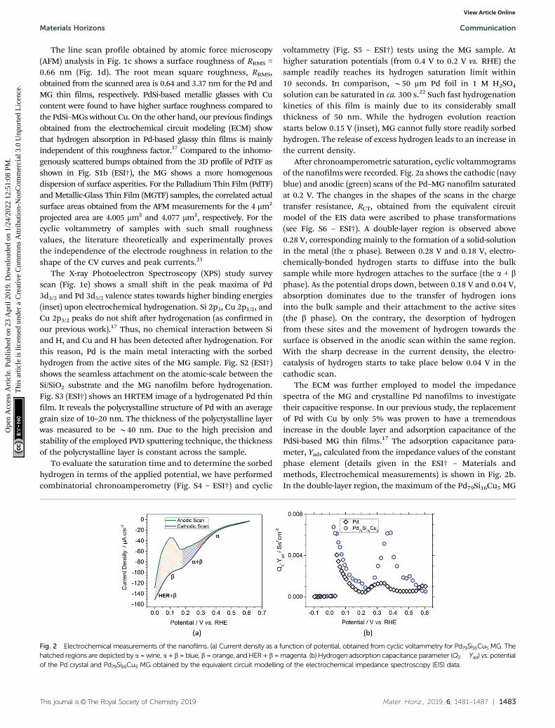
A schematic of the hydrogenation mechanism is shown inFig. 3a. The adsorbed hydrogen ions on the surface penetrateinto bulk Pd,23 in turn reaching the Si substrate which acts as abarrier. The accumulation of the hydrogen ions at the interfaceleads to the formation of palladium hydride crystals (indicatedby yellow and gray atoms). The increase of the hydrogenation inpalladium hydride crystals generates an outward pressureleading to nanobubble formation. The excess H+ ions diffuseout directly or through small chimneys, and depending on theapplied potential, might subsequently leave the surface throughreduction in the form of hydrogen gas.24 Aberration-correctedhigh-resolution transmission electron microscopy was used toinvestigate the reasons behind the dramatic changes in thePd–MG nanofilms upon hydrogenation. Fig. 3c and d show thespatially dispersed nanobubble formation along the nanofilm.Fig. S7a (ESI†) is an enlarged image of these nanobubbles takenby HRSTEM. HRTEM images taken from 3 different regions(Fig. 3b and Fig. S7b – ESI†) show a clear contrast between thebubbles and the MG matrix. Fig. 3c shows a bright-field TEMimage of the Si–MG assembly. Bubble-shaped structures emanatingfrom the substrate surface expand and generate nanobumps on thenanofilm surface. The HAADF-STEM images in Fig. 3d displaythe nanobubbles forming on the Si substrate. The matrixaround the bubbles is slightly darker than the other regionsindicating that the MG is pushed outwards due to hydrogenation.
Although no clear nanosegregation was observed in the MGmatrix, Si depletion of around 4% in the very surrounding ofthe nanobubbles was determined from the image analyses ofthe EELS data. Thin nanohumps were formed on the top surfaceof the MG due to the outward pressure of the accumulatedhydrogen at the interface.
Fig. S8a (ESI†) shows a HAADF-STEM image of electroche-mically hydrogenated polycrystalline Pd. Fig. S8b (ESI†) showsthe elemental mapping of Pd, Si and the interlayer SiO2. The Pdcontent is uniform across the sample, which was confirmed byEELS mapping. From the micrographs, no palladium hydridecan be detected at the interface between the Si substrate and thecrystalline Pd nanofilm. This result confirms that the nanobubbleformation is unique to Pd79Si16Cu5 nanofilms. The thickness mapof the MG nanofilm in Fig. S9a (ESI†) shows that the relativespecimen thickness t/l (thickness expressed in units of theinelastic mean free path) decreases severely (from 0.7 to 0.6 t/l)during nanobubble formation. On the other hand, the strongdecrease in thickness as shown in Fig. S9b (ESI†) is mainly dueto the contribution of diffraction scattering from the polycrystal-line structure of Pd.
The HRTEM micrograph of a Pd–MG nanofilm provided inFig. 4a reveals the structural differences between the unhydro-genated regions (Fig. 4c(1)) and the hydrogenated regions inthe vicinity of the nanobubbles (Fig. 4c(2)). The compositionanalysis of all the investigated and individual elements per-formed by EELS is depicted in Fig. 4b. Region 1 constitutes amaze-like structure with a broad diffuse halo on the fast Fouriertransform (FFT) pattern of the HRTEM image (Fig. 4d(1)). Onthe other hand, palladium hydride crystals are observed on thetop or back layer of the nanobubbles, where point maxima onthe broad diffuse FFT pattern can be seen in Fig. 4d(2). Thesuperimposed FFT pattern of the first and second regions(Fig. 4d) shows that the two main lattice fringes found in theFFT pattern from the region close to the nanobubble correspondto fcc-Pd and fcc-PdHx nanocrystals with (111) (0.225 nm and0.2286 nm, inside rings) and (200) (0.194 nm and 0.198 nm,
Fig. 3 Palladium hydride formation around the nanobubbles by means of chronoamperometric saturation is schematically described in (a). Visualizationof nanobubbles in the MG nanofilms via (b) HRTEM, (c) low magnification BFTEM and (d) STEM-HAADF. A Pt layer of B50 nm behind the nanobumps iscoated on the MG film for the TEM sample preparation by FIB.
Communication Materials Horizons
Ope
n A
cces
s A
rtic
le. P
ublis
hed
on 2
3 A
pril
2019
. Dow
nloa
ded
on 1
/24/
2022
12:
51:0
8 PM
. T
his
artic
le is
lice
nsed
und
er a
Cre
ativ
e C
omm
ons
Attr
ibut
ion-
Non
Com
mer
cial
3.0
Unp
orte
d L
icen
ce.
View Article Online
This journal is©The Royal Society of Chemistry 2019 Mater. Horiz., 2019, 6, 1481--1487 | 1485
outside rings) planes, respectively. The magnified image of ananobubble as shown in Fig. 4e reveals that the diameters of thenanocrystals range from 1 to 4 nm, confirming the formation ofextremely small crystals around the hydrided regions.
The HRTEM and HAADF-STEM micrographs reveal that themajority of the large bubbles initiate from the Si–MG interface.This is mainly because the hydrogen ions, dissociated from thediluted sulfuric acid solution via the applied potential, propagatetowards the inner layers until reaching the Si substrate which actsas a barrier. Several nanometers of SiO2 layer on the substratemediates the H+ entrapment due to the partial negative charge ofoxygen and results in Si–O� � �H formation.25 The entrappedhydrogen ions subsequently give electrons to palladium, whichleads to PdHx formation. The increase in the hydrogen contentas a function of the applied voltage in turn forms an innerdiaphragm and a nanobump on the MG surface. Smallerbubbles generated from the big bubble and from the interface,as well as hydrogen pathways towards the top surface of thenanofilm, are observed. The kinetic energy of the hydrogen ionscan be further accelerated by optimizing the applied potentialand time of hydrogenation, which would in turn influence thediameter and number of nanobubbles. The maximum solubilityof hydrogen in the b-phase is B35 times larger than that in thea-phase. The diffusion coefficient of hydrogen in the b-phase isB3.33 times larger than that for the a-phase (ratios calculatedfrom ref. 22). Furthermore, our chronoamperometry and CVstudies have shown that (de)hydrogenation occurs in a matter ofseconds. Hence, the adopted Si–MG assembly can partially becharged and discharged by hydrogen at fast rates and withoutthe need of generating new nanobubbles. From this study, it isdeduced that the Si/SiO2 substrate plays a key role in hetero-genous nucleation of PdHx crystals from the surface. Besides the
Si/SiO2 and MG interface, artificial interfaces such as pores orsecond phases can be introduced from which the nanobubblescould nucleate via palladium hydride formation. On the otherhand, polycrystalline Pd nanofilms produced by using the samePVD method do not exhibit such nanobubble formation even afterreaching the hydrogen saturation limit via chronoamperometry.This confirms that hydrogen cannot effectively penetrate into thebulk layers of the Pd polycrystal nanofilm. Another problem is thatthe hydrogen atoms can reside only at the interstitial sites of thepolycrystalline Pd, which limits the amount of hydrogen turninginto the hydride form.
Fig. S10a–c (ESI†) shows the SAED patterns taken from thesuperposition of the diffraction of the hydrogenated Pd nanofilm(Fig. S10a, ESI†), the individual Si substrate (Fig. S10b, ESI†) andthe Pt layer (Fig. S10c, ESI†). Hereafter we analyzed the HRTEMimages taken from the Pd nanofilm (Fig. S10d and f, ESI†) andthe HRTEM image of the Pt layer as a reference (Fig. S10e, ESI†).Fig. S10g (ESI†) shows the azimuthal profile of the FFT patternstaken separately from the Pt layer and the hydrogenated Pd film.The shift of the peak positions of the hydrogenated Pd film towardssmaller reciprocal values (larger real space values) is clearly visible.Both peaks correspond to the (111) and (200) planes of an fccstructure. The average lattice constants for the Pt layer and thehydrogenated Pd film are measured as 0.392 � 0.002 nm and0.402 � 0.002 nm, respectively. The lattice constant of thehydrogenated polycrystalline Pd film has the same value aspreviously reported.26 Thus, the value for the hydrogenatedPd film is 0.402 � 0.002 nm, which is much larger than theoriginal Pd (fcc) lattice constant of afcc_Pd = 0.389 � 0.002 nm asconfirmed by the literature.26,27
In contrast to the crystalline Pd film the amount of latticeexpansion in MG films is more difficult to estimate due to the
Fig. 4 High-resolution chemical composition study of the Pd–MG nanofilm. (a) HAADF-STEM and (b) EELS analysis of the assembly. Pink color indicatesthe high abundance of Pd with relatively lower Si, where traces of oxygen obtained from the SiO2 layer are observed. Individual Pd (red), O (green) and Si(blue) compositions within the Pd–MG nanofilm are shown. Due to the origin of the dark-field image, a minimum amount of signal can be attained fromthe porous regions (observed in black). Structural evaluation of the hydrogenated MG nanofilm. (c) Recorded HRTEM images obtained from the(1) unhydrogenated amorphous and (2) nanobubble containing palladium hydride nanocrystals. (d) Corresponding superimposed FFT patterns exhibitinga broad diffuse halo for (1), and point maxima on the broad halo for (2) (separated FFTs are given in the insets). The continuous and dashed linescorrespond to the lattice fringes of the fcc Pd and Pd–H nanocrystals, respectively. The outer and inner rings represent the (200) and (111) planes,respectively. (e) Magnified view of the hydride regions with nanocrystals of diameters ranging from 1 to 4 nm.
Materials Horizons Communication
Ope
n A
cces
s A
rtic
le. P
ublis
hed
on 2
3 A
pril
2019
. Dow
nloa
ded
on 1
/24/
2022
12:
51:0
8 PM
. T
his
artic
le is
lice
nsed
und
er a
Cre
ativ
e C
omm
ons
Attr
ibut
ion-
Non
Com
mer
cial
3.0
Unp
orte
d L
icen
ce.
View Article Online
1486 | Mater. Horiz., 2019, 6, 1481--1487 This journal is©The Royal Society of Chemistry 2019
lack of long range order in metallic glasses. Fig. S11a and c(ESI†) show additional HRTEM images of the MG nanofilmsafter hydrogenation. It is clearly seen that from the FFTpatterns in Fig. S11b and d (ESI†) the appearance of thediffraction spots superimposed on the diffuse ring from theamorphous matrix. These spots correspond to the formation ofthe palladium hydride nanocrystals at the nanobubble locations.The contribution of Pd hydride formed within the amorphousMG matrix is marked also by the red dashed line on theazimuthal profile of the FFT pattern shown in Fig. S11e (ESI†)which corresponds to 0.232 � 0.002 nm of (111) PdHx, and acalculated lattice parameter of 0.402 � 0.002 nm. Moreover,Fig. S11e (ESI†) shows that the peak position of the broadmaximum obtained from the MG matrix shifts to 0.225� 0.002 nmin comparison to the as-sputtered sample at 0.220 � 0.001 nmobtained from the maximum of the first diffuse peak (20.541determined from the pseudo-Voigt fit of the XRD diffractogramas shown in Fig. 1b). Thus, although we cannot directly comparethe difference in the lattice expansions of the MG and poly-crystalline Pd films, from the measured average atomic distancesof the initial MG film we calculate the fcc lattice parameter of thevery first Pd hydride crystals formed within the MG matrix as0.380 nm. This value is lower than that of the initial polycrystal-line Pd nanofilms of 0.389 nm. Upon hydrogen saturation thelattice parameter of the crystalline PdHx phase reaches the samelattice constant of 0.402 nm. Since the volumetric expansiondifference is on the third power, a huge volumetric expansion isobserved for the MG films, which can be assigned to the abundanceof free volume acting as the active sites for the hydrogenentrapment. The average volumetric expansion, V = VPdHx
� VPd,for Pd and Pd79Si16Cu5 nanofilms is calculated as 6.10 Å3 and10.09 Å3, respectively. These results indicate that the latticeexpansion of selected MG after hydrogen saturation is higherthan any Pd alloys under ambient conditions.28 In fact, hydro-gen in b palladium hydride is commonly accepted to be byoctahedral interstitial site occupation of an fcc unit cell, whichleads to a theoretical limiting H to Pd ratio of 1 (H/M = 0.7).7,29
Thus, the amount of hydrogen entrapment is much less, whichis not sufficient to generate nanobubbles. On the other hand,for the Pd–Si–Cu MG system, Pd-centered trigonal prismscapped with Cu atoms, as obtained from neutron diffractionexperiments and molecular dynamics simulations, might resultin the generation of more sites that are active for hydrogenentrapment.19,20,30,31 Moreover, due to the abundance of free volumebetween the atomic clusters as seen in atomic simulations,32,33 thehydrogen ions can easily pass through the amorphous matrix andaccumulate at the interface. The loosely packed structure withrandomly dispersed interstitial holes in the supercooled liquid phaseand its sluggish crystallization kinetics are the main reasons for thehigh abundance of such active sites.34,35 Thus, a higher entrapmentof hydrogen in ion form can be attained, leading to the unit cellexpansion of the formed PdHx crystals.
H/M ratio vs. applied potential graphs in Fig. S12 (ESI†)clearly show that the rate of hydrogenation increases below0.15 V for both samples. The H/M ratio for the Pd nanofilmalready starts with 0.62 after the chronoamperometric saturation
for 850 s at 0.6 V. This clearly means that MG can readily sorbsimilar amounts of hydrogen to the maximum saturation limit ofhydrogen in Pd. The maximum H/M ratios observed for theconsidered range are 0.61 and 1.56 for the Pd and MG nanofilms,respectively. Thus, around 2.5 times higher hydrogen sorption ispossible with the MG nanofilm. The increase in H/M values andthe trend of increase towards smaller potentials are in line with theprevious finding conducted in an acidic environment with Pdnanoparticles.36 The corresponding maximum weight percent ofhydrogen (max. wt% H) for the Pd and MG nanofilms is 0.57 and1.48%, respectively. This finding correlates well with literaturevalues of H/M and max. wt% H of pristine Pd,2,37–40 where smalldifferences can be due to the electrolyte concentration/type, as wellas the Si substrate used in this study. The hydrogen storagecapacity of the selected MG nanofilms is comparable to manyother conventionally used materials such as Mg2Ni, Ti, V, Zr,LaNi5, FeTi, Cu–Ni, TiFe, TiS2 and even the newly discovered highentropy alloys.2,28,41–44 As confirmed by the HRTEM, the hydro-genation is more favored in the heterogenous nucleation sites.Thus, further control or design of such interfaces might enhancethe amount of stored hydrogen.
Table S1 (ESI†) summarizes hydrogen sorption of differentmaterials such as Mg-rich powders, complex light-metal hydrides,carbon nanotubes, zeolites, metal organic frameworks, hydrideslurries, aerogels, liquid/compressed hydrogen, high entropyalloys, and metallic glasses in terms of maximum weight percentof stored hydrogen (wt% of H) and the atomic ratio of hydrogen tometal (H/M). Compared to many other metal-hydride formers, Pdexhibits long-term cycling stability up to 2500 cycles,45 andexcellent kinetic hydrogen reversibility due to a very low enthalpyof formation of hydride in Pd.41,46 In terms of electrocatalyticactivity of the selected MG film, our recent findings obtainedfrom the Tafel plots exhibit a slightly smaller Tafel slope andhigher exchange current density, revealing that the H2 evolutionkinetics is faster than that of the Pd nanofilms.
Conclusions
In this contribution, we assessed the electrosorption capacity ofhydrogen in PVD-sputtered Pd79Si16Cu5 MG nanofilms ofB50 nm thickness comparatively with Pd polycrystalline specimens.Palladium hydride in the amorphous nanofilm is formed in thevicinity of nanobubbles, which originates from its interface with theSi substrate. HRTEM images corroborate the presence of crystals,1 to 4 nm in diameter, spatially dispersed around the nano-bubbles. From the corresponding FFT pattern comparisonacquired from the hydride regions and the fully amorphousmatrix, a volume expansion of 10.09 Å3 is found. On the otherhand, for hydrogenated polycrystalline Pd, the volume expansionis only 6.10 Å3, which is in agreement with previous findings. Thecalculated ratio of H/M = 1.56 of the Pd79Si16Cu5 MG nanofilmsobtained from the electrochemical hydrogenation, which isaround 2.5 times larger than that of the Pd nanofilms, placesthem among promising materials for future energy systems.
Communication Materials Horizons
Ope
n A
cces
s A
rtic
le. P
ublis
hed
on 2
3 A
pril
2019
. Dow
nloa
ded
on 1
/24/
2022
12:
51:0
8 PM
. T
his
artic
le is
lice
nsed
und
er a
Cre
ativ
e C
omm
ons
Attr
ibut
ion-
Non
Com
mer
cial
3.0
Unp
orte
d L
icen
ce.
View Article Online
This journal is©The Royal Society of Chemistry 2019 Mater. Horiz., 2019, 6, 1481--1487 | 1487
Conflicts of interest
The authors declare no financial interest.
Acknowledgements
The authors commemorate Dipl-Ing Dr Mont. T. Schoberl, whowas involved in performing the AFM study and who tragicallylost his life in a traffic accident. The authors thank P. Zeffererfor technical support, C. Mitterer and B. Putz for providing thesputtering device for synthesizing the MG and Pd nanofilms,and S. Ketov, and C. Gammer for fruitful discussions. Theauthors thank Prof. Andrey Chuvilin from CIC NanoGUNE,Spain, for technical support of TEM experiments and fruitfuldiscussions. This work was supported by the EuropeanResearch Council under the Advanced Grants ‘‘INTELHYB –Next generation of complex metallic materials in intelligenthybrid structures’’ (Grant ERC-2013-ADG-340025) and ‘‘ExtendGlass– Extending the range of the glassy state: Exploring structure andproperty limits in metallic glasses’’ (Grant ERC-2015-ADG-695487).Yu. P. I. acknowledges support under the grant no 3.7383.2017/8.9of the Ministry of Science and Higher Education (Russia).
References
1 P. Preuster, A. Alekseev and P. Wasserscheid, Annu. Rev.Chem. Biomol. Eng., 2017, 8, 445–471.
2 B. D. Adams and A. C. Chen, Mater. Today, 2011, 14, 282–289.3 L. P. Bicelli, Int. J. Hydrogen Energy, 1986, 11, 555–562.4 D. L. Cummings and G. J. Powers, Ind. Eng. Chem. Process
Des. Dev., 1974, 13, 182–192.5 N. A. A. Rusman and M. Dahari, Int. J. Hydrogen Energy,
2016, 41, 12108–12126.6 B. Sakintuna, F. Lamari-Darkrim and M. Hirscher, Int.
J. Hydrogen Energy, 2007, 32, 1121–1140.7 L. L. Jewell and B. H. Davis, Appl. Catal., A, 2006, 310, 1–15.8 T. Tanaka, M. Keita and D. E. Azofeifa, Phys. Rev. B: Condens.
Matter Mater. Phys., 1981, 24, 1771–1776.9 L. Johnson, E. E. Donaldson and M. J. Dresser, J. Vac. Sci.
Technol., 1972, 9, 857–860.10 The Engineering ToolBox, https://www.engineeringtoolbox.
com/fuels-higher-calorific-values-d_169.html, accessed 29/08/2018.
11 M. U. Niemann, S. S. Srinivasan, A. R. Phani, A. Kumar, D. Y.Goswami and E. K. Stefanakos, J. Nanomater., 2008, 950967.
12 W. Grochala and P. P. Edwards, Chem. Rev., 2004, 104,1283–1316.
13 X. Li, Z. N. Wang, Z. R. Zhang, G. Yang, M. S. Jin, Q. Chenand Y. D. Yin, Mater. Horiz., 2017, 4, 584–590.
14 F. L. Meng, Z. W. Chang, J. J. Xu, X. B. Zhang and J. M. Yan,Mater. Horiz., 2018, 5, 298–302.
15 G. Jimenez, E. Dillon, J. Dahlmeyer, T. Garrison, T. Garrison,S. Darkey, K. Wald, J. Kubik, D. Paciulli, M. Talukder, J. Nott,M. Ferrer, J. Prinke, P. Villaneuva, F. Massicotte, K. Rebeiz,S. Nesbit and A. Craft, Adv. Chem. Eng. Sci., 2016, 06, 246–261.
16 T. B. Massalski, Y. W. Kim, L. F. Vassamillet and R. W. Hopper,Mater. Sci. Eng., 1981, 47, P1–P11.
17 B. Sarac, T. Karazehir, M. Muhlbacher, B. Kaynak, C. Gammer,T. Schoberl, A. S. Sarac and J. Eckert, ACS Appl. Energy Mater.,2018, 1, 2630–2646.
18 F. Spaepen, Scr. Mater., 2006, 54, 363–367.19 G. Q. Yue, Y. Zhang, Y. Sun, B. Shen, F. Dong, Z. Y. Wang,
R. J. Zhang, Y. X. Zheng, M. J. Kramer, S. Y. Wang, C. Z. Wang,K. M. Ho and L. Y. Chen, Sci. Rep., 2015, 5, 08277.
20 S. Kajita, S. Kohara, Y. Onodera, T. Fukunaga and E. Matsubara,Mater. Trans., 2011, 52, 1807–1813.
21 D. Menshykau, I. Streeter and R. G. Compton, J. Phys. Chem.C, 2008, 112, 14428–14438.
22 P. Millet, M. Srour, R. Faure and R. Durand, Electrochem.Commun., 2001, 3, 478–482.
23 C. Gabrielli, P. P. Grand, A. Lasia and H. Perrot, J. Electrochem.Soc., 2004, 151, A1925–A1936.
24 A. R. Kucernak and C. Zalitis, J. Phys. Chem. C, 2016, 120,10721–10745.
25 A. G. Revesz, J. Electrochem. Soc., 1979, 126, 122–130.26 A. Maeland and T. B. Flanagan, J. Phys. Chem., 1964, 68,
1419–1426.27 B. N. Dutta and B. Dayal, Phys. Status Solidi, 1963, 3, 2253–2259.28 B. Baranowski, S. Majchrzak and T. B. Flanagan, J. Phys. F:
Met. Phys., 1971, 1, 258–261.29 R. Caputo and A. Alavi, Mol. Phys., 2003, 101, 1781–1787.30 T. Fukunaga and K. Suzuki, Sci. Rep., 1980, 28, 208–217.31 T. Fukunaga and K. Suzuki, Sci. Rep., 1981, 29, 153–175.32 C. Fan, P. K. Liaw and C. T. Liu, Intermetallics, 2009, 17, 86–87.33 L. Ward, D. Miracle, W. Windl, O. N. Senkov and K. Flores,
Phys. Rev. B: Condens. Matter Mater. Phys., 2013, 88, 134205.34 R. Busch, A. Masuhr, E. Bakke and W. L. Johnson, Mater.
Sci. Forum, 1998, 269–272, 547.35 L. Z. Zhao, R. J. Xue, Z. G. Zhu, Z. Lu, E. Axinte, W. H. Wang
and H. Y. Bai, J. Appl. Phys., 2014, 116, 103516.36 R. K. Singh, R. Ramesh, R. Devivaraprasad, A. Chakraborty
and M. Neergat, Electrochim. Acta, 2016, 194, 199–210.37 F. A. Lewis, Platinum Met. Rev., 1960, 4, 132–137.38 L. Birry and A. Lasia, Electrochim. Acta, 2006, 51, 3356–3364.39 M. Łukaszewski, K. Hubkowska, U. Koss and A. Czerwinski,
Materials, 2013, 6, 4817–4835.40 M. Baldauf and D. M. Kolb, Electrochim. Acta, 1993, 38, 2145–2153.41 R. Kirchheim and A. Pundt, in Physical Metallurgy ed. D. E.
Laughlin and K. Hono, Elsevier, Oxford, 5th edn, 2014, ch. 25,pp. 2597–2705, DOI: 10.1016/B978-0-444-53770-6.00025-3.
42 D. Karlsson, G. Ek, J. Cedervall, C. Zlotea, K. T. Moller,T. C. Hansen, J. Bednarcik, M. Paskevicius, M. H. Sorby,T. R. Jensen, U. Jansson and M. Sahlberg, Inorg. Chem.,2018, 57, 2103–2110.
43 M. Sahlberg, D. Karlsson, C. Zlotea and U. Jansson, Sci. Rep.,2016, 6, 36770.
44 J. Chen, S. L. Li, Z. L. Tao, Y. T. Shen and C. X. Cui, J. Am.Chem. Soc., 2003, 125, 5284–5285.
45 T. Mittermeier, A. Weiss, H. A. Gasteiger and F. Hasche,J. Electrochem. Soc., 2017, 164, F1081–F1089.
46 E. Fromm and G. Horz, Int. Met. Rev., 1980, 25, 269–311.
Materials Horizons Communication
Ope
n A
cces
s A
rtic
le. P
ublis
hed
on 2
3 A
pril
2019
. Dow
nloa
ded
on 1
/24/
2022
12:
51:0
8 PM
. T
his
artic
le is
lice
nsed
und
er a
Cre
ativ
e C
omm
ons
Attr
ibut
ion-
Non
Com
mer
cial
3.0
Unp
orte
d L
icen
ce.
View Article Online