Ultra Low Power Boost Converter with Battery · PDF filebq25504 Ultra Low-Power Boost...
36
1 2 4 3 5 6 7 8 9 10 11 12 16 15 14 13 ` CHVR L BST CSTOR VSTOR VBAT_OK bq25504 Solar Cell + - ROC1 ROC2 CREF ROV1 ROV2 RUV1 RUV2 ROK1 ROK2 R OK3 Battery SYSTEM LOAD VSS VIN_DC AVSS VOC_SAMP VREF_SAMP OT_PROG VBAT_OV VRDIV VBAT_UV LBST VSTOR VBAT VSS OK_HYST OK_PROG VBAT_OK CFLTR Product Folder Sample & Buy Technical Documents Tools & Software Support & Community bq25504 SLUSAH0C – OCTOBER 2011 – REVISED JUNE 2015 bq25504 Ultra Low-Power Boost Converter With Battery Management for Energy Harvester Applications 1 Features 3 Description The bq25504 device is the first of a new family of 1• Ultra Low-Power With High-Efficiency DC-DC intelligent integrated energy harvesting nano-power Boost Converter/Charger management solutions that are well suited for – Continuous Energy Harvesting From Low-Input meeting the special needs of ultra low power Sources: V IN ≥ 80 mV (Typical) applications. The device is specifically designed to efficiently acquire and manage the microwatts (μW) – Ultra-Low Quiescent Current: I Q < 330 nA to miliwatts (mW) of power generated from a variety (Typical) of DC sources like photovoltaic (solar) or thermal – Cold-Start Voltage: V IN ≥ 330 mV (Typical) electric generators. The bq25504 is the first device of • Programmable Dynamic Maximum Power Point its kind to implement a highly efficient boost Tracking (MPPT) converter/charger targeted toward products and systems, such as wireless sensor networks (WSNs) – Integrated Dynamic Maximum Power Point which have stringent power and operational Tracking for Optimal Energy Extraction From a demands. The design of the bq25504 starts with a Variety of Energy Generation Sources DC-DC boost converter/charger that requires only – Input Voltage Regulation Prevents Collapsing microwatts of power to begin operating. Input Source Once started, the boost converter/charger can • Energy Storage effectively extract power from low-voltage output – Energy Can be Stored to Rechargeable Li-ion harvesters such as thermoelectric generators (TEGs) Batteries, Thin-film Batteries, Super- or single- or dual-cell solar panels. The boost Capacitors, or Conventional Capacitors converter can be started with V IN as low as 330 mV, and once started, can continue to harvest energy • Battery Charging and Protection down to V IN = 80 mV. – User Programmable Undervoltage and Overvoltage Levels Device Information (1) – On-Chip Temperature Sensor With PART NUMBER PACKAGE BODY SIZE (NOM) Programmable Overtemperature Shutoff bq25504 VQFN (16) 3.00 mm x 3.00 mm • Battery Status Output (1) For all available packages, see the orderable addendum at the end of the datasheet. – Battery Good Output Pin – Programmable Threshold and Hysteresis Solar Application Circuit – Warn Attached Microcontrollers of Pending Loss of Power – Can be Used to Enable or Disable System Loads 2 Applications • Energy Harvesting • Solar Chargers • Thermal Electric Generator (TEG) Harvesting • Wireless Sensor Networks (WSNs) • Industrial Monitoring • Environmental Monitoring • Bridge and Structural Health Monitoring (SHM) • Smart Building Controls • Portable and Wearable Health Devices • Entertainment System Remote Controls 1 An IMPORTANT NOTICE at the end of this data sheet addresses availability, warranty, changes, use in safety-critical applications, intellectual property matters and other important disclaimers. PRODUCTION DATA.
Transcript of Ultra Low Power Boost Converter with Battery · PDF filebq25504 Ultra Low-Power Boost...

1
2
4
3
5 6 7 8
9
10
11
12
16 15 14 13`
CHVR
LBSTCSTOR
VSTOR
VBAT_OK
bq25504
Solar
Cell
+
-
ROC1
ROC2
CREF
ROV1
ROV2
RUV1
RUV2
ROK1
ROK2
ROK3
BatterySYSTEM
LOAD
VSS
VIN_DC
AVSS
VOC_SAMP
VREF_SAMP
OT_PROG VBAT_OV VRDIV VBAT_UV
LBST VSTOR VBAT VSS
OK_HYST
OK_PROG
VBAT_OK
CFLTR
Product
Folder
Sample &Buy
Technical
Documents
Tools &
Software
Support &Community
bq25504SLUSAH0C –OCTOBER 2011–REVISED JUNE 2015
bq25504 Ultra Low-Power Boost Converter With Battery Management for EnergyHarvester Applications
1 Features 3 DescriptionThe bq25504 device is the first of a new family of
1• Ultra Low-Power With High-Efficiency DC-DCintelligent integrated energy harvesting nano-powerBoost Converter/Chargermanagement solutions that are well suited for
– Continuous Energy Harvesting From Low-Input meeting the special needs of ultra low powerSources: VIN ≥ 80 mV (Typical) applications. The device is specifically designed to
efficiently acquire and manage the microwatts (µW)– Ultra-Low Quiescent Current: IQ < 330 nAto miliwatts (mW) of power generated from a variety(Typical)of DC sources like photovoltaic (solar) or thermal– Cold-Start Voltage: VIN ≥ 330 mV (Typical) electric generators. The bq25504 is the first device of
• Programmable Dynamic Maximum Power Point its kind to implement a highly efficient boostTracking (MPPT) converter/charger targeted toward products and
systems, such as wireless sensor networks (WSNs)– Integrated Dynamic Maximum Power Pointwhich have stringent power and operationalTracking for Optimal Energy Extraction From ademands. The design of the bq25504 starts with aVariety of Energy Generation SourcesDC-DC boost converter/charger that requires only
– Input Voltage Regulation Prevents Collapsing microwatts of power to begin operating.Input Source
Once started, the boost converter/charger can• Energy Storage effectively extract power from low-voltage output– Energy Can be Stored to Rechargeable Li-ion harvesters such as thermoelectric generators (TEGs)
Batteries, Thin-film Batteries, Super- or single- or dual-cell solar panels. The boostCapacitors, or Conventional Capacitors converter can be started with VIN as low as 330 mV,
and once started, can continue to harvest energy• Battery Charging and Protectiondown to VIN = 80 mV.– User Programmable Undervoltage and
Overvoltage Levels Device Information(1)
– On-Chip Temperature Sensor With PART NUMBER PACKAGE BODY SIZE (NOM)Programmable Overtemperature Shutoff bq25504 VQFN (16) 3.00 mm x 3.00 mm
• Battery Status Output (1) For all available packages, see the orderable addendum atthe end of the datasheet.– Battery Good Output Pin
– Programmable Threshold and HysteresisSolar Application Circuit
– Warn Attached Microcontrollers of PendingLoss of Power
– Can be Used to Enable or Disable SystemLoads
2 Applications• Energy Harvesting• Solar Chargers• Thermal Electric Generator (TEG) Harvesting• Wireless Sensor Networks (WSNs)• Industrial Monitoring• Environmental Monitoring• Bridge and Structural Health Monitoring (SHM)• Smart Building Controls• Portable and Wearable Health Devices• Entertainment System Remote Controls
1
An IMPORTANT NOTICE at the end of this data sheet addresses availability, warranty, changes, use in safety-critical applications,intellectual property matters and other important disclaimers. PRODUCTION DATA.
bq25504SLUSAH0C –OCTOBER 2011–REVISED JUNE 2015 www.ti.com
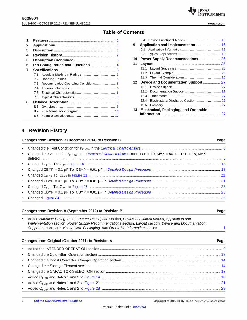
Table of Contents8.4 Device Functional Modes........................................ 131 Features .................................................................. 1
9 Application and Implementation ........................ 162 Applications ........................................................... 19.1 Application Information............................................ 163 Description ............................................................. 19.2 Typical Applications ................................................ 184 Revision History..................................................... 2
10 Power Supply Recommendations ..................... 255 Description (Continued) ........................................ 311 Layout................................................................... 256 Pin Configuration and Functions ......................... 4
11.1 Layout Guidelines ................................................. 257 Specifications......................................................... 511.2 Layout Example .................................................... 267.1 Absolute Maximum Ratings ..................................... 511.3 Thermal Considerations ........................................ 267.2 Handling Ratings....................................................... 5
12 Device and Documentation Support ................. 277.3 Recommended Operating Conditions....................... 512.1 Device Support...................................................... 277.4 Thermal Information .................................................. 512.2 Documentation Support ........................................ 277.5 Electrical Characteristics........................................... 612.3 Trademarks ........................................................... 277.6 Typical Characteristics .............................................. 712.4 Electrostatic Discharge Caution............................ 278 Detailed Description .............................................. 912.5 Glossary ................................................................ 278.1 Overview ................................................................... 9
13 Mechanical, Packaging, and Orderable8.2 Functional Block Diagram ....................................... 10Information ........................................................... 278.3 Feature Description................................................. 10
4 Revision History
Changes from Revision B (December 2014) to Revision C Page
• Changed the Test Condition for PIN(CS) in the Electrical Characteristics ............................................................................... 6• Changed the values for PIN(CS) in the Electrical Characteristics From: TYP = 10, MAX = 50 To: TYP = 15, MAX
deleted ................................................................................................................................................................................... 6• Changed CFLTR To: CBYP Figure 14 ..................................................................................................................................... 18• Changed CBYP = 0.1 µF To: CBYP = 0.01 µF in Detailed Design Procedure .................................................................... 18• Changed CFLTR To: CBYP in Figure 21 .................................................................................................................................. 21• Changed CBYP = 0.1 µF To: CBYP = 0.01 µF in Detailed Design Procedure .................................................................... 21• Changed CFLTR To: CBYP in Figure 28 ................................................................................................................................. 23• Changed CBYP = 0.1 µF To: CBYP = 0.01 µF in Detailed Design Procedure .................................................................... 23• Changed Figure 34 .............................................................................................................................................................. 26
Changes from Revision A (September 2012) to Revision B Page
• Added Handling Rating table, Feature Description section, Device Functional Modes, Application andImplementation section, Power Supply Recommendations section, Layout section, Device and DocumentationSupport section, and Mechanical, Packaging, and Orderable Information section................................................................ 1
Changes from Original (October 2011) to Revision A Page
• Added the INTENDED OPERATION section ......................................................................................................................... 9• Changed the Cold -Start Operation section ......................................................................................................................... 13• Changed the Boost Converter, Charger Operation section.................................................................................................. 14• Changed the Storage Element section................................................................................................................................. 14• Changed the CAPACITOR SELECTION section ................................................................................................................. 17• Added CFLTR and Notes 1 and 2 to Figure 14 ..................................................................................................................... 18• Added CFLTR and Notes 1 and 2 to Figure 21 ..................................................................................................................... 21• Added CFLTR and Notes 1 and 2 to Figure 28 ..................................................................................................................... 23
2 Submit Documentation Feedback Copyright © 2011–2015, Texas Instruments Incorporated
Product Folder Links: bq25504

bq25504www.ti.com SLUSAH0C –OCTOBER 2011–REVISED JUNE 2015
5 Description (Continued)The bq25504 also implements a programmable maximum power point tracking sampling network to optimize thetransfer of power into the device. Sampling the VIN_DC open-circuit voltage is programmed using externalresistors, and held with an external capacitor (CREF).
For example solar cells that operate at maximum power point (MPP) of 80% of their open-circuit voltage, theresistor divider can be set to 80% of the VIN_DC voltage and the network will control the VIN_DC to operatenear that sampled reference voltage. Alternatively, an external reference voltage can be provide by a MCU toproduce a more complex MPPT algorithm.
The bq25504 was designed with the flexibility to support a variety of energy storage elements. The availability ofthe sources from which harvesters extract their energy can often be sporadic or time-varying. Systems willtypically need some type of energy storage element, such as a rechargeable battery, super capacitor, orconventional capacitor. The storage element ensures that constant power is available when needed for thesystems. The storage element also allows the system to handle any peak currents that cannot directly come fromthe input source.
To prevent damage to a customer’s storage element, both maximum and minimum voltages are monitoredagainst the user programmed undervoltage (UV) and overvoltage (OV) levels.
To further assist users in the strict management of their energy budgets, the bq25504 toggles the battery goodflag to signal an attached microprocessor when the voltage on an energy storage battery or capacitor hasdropped below a preset critical level. This warning should trigger the shedding of load currents to prevent thesystem from entering an undervoltage condition. The OV, UV, and battery good thresholds are programmedindependently.
All the capabilities of bq25504 are packed into a small-footprint, 16-lead, 3-mm x 3-mm VQFN package.
Copyright © 2011–2015, Texas Instruments Incorporated Submit Documentation Feedback 3
Product Folder Links: bq25504

1
2
4
3
5 6 7 8
9
10
11
12
16 15 14 13`
bq25504
VSS
VIN_DC
AVSS
VOC_SAMP
VREF_SAMP
OT_PROG VBAT_OV VRDIV VBAT_UV
LBST VSTOR VBAT VSS
OK_HYST
OK_PROG
VBAT_OK
bq25504SLUSAH0C –OCTOBER 2011–REVISED JUNE 2015 www.ti.com
6 Pin Configuration and Functions
RGT Package16 Pins
Top View
Pin FunctionsPIN
I/O DESCRIPTIONNAME NO.AVSS 12 Supply Signal ground connection for the device
Inductor connection for the boost charger switching node. Connect a 22 µH inductor between thisLBST 16 Input pin and pin 2 (VIN_DC).Connect to the mid-point of external resistor divider between VRDIV and GND for setting theOK_HYST 9 Input VBAT_OK hysteresis threshold. If not used, connect this pin to GND.Connect to the mid-point of external resistor divider between VRDIV and GND for setting theOK_PROG 10 Input VBAT_OK threshold. If not used, connect this pin to GND.Digital Programming input for IC overtemperature threshold. Connect to GND for 60 C threshold orOT_PROG 5 Input VSTOR for 120 C threshold.
VBAT 14 I/O Connect a rechargeable storage element with at least 100 uF of equivalent capacitance to this pin.Digital output for battery good indicator. Internally referenced to the VSTOR voltage. Leave floatingVBAT_OK 11 Output if not used.Connect to the mid-point of external resistor divider between VRDIV and GND for setting theVBAT_OV 6 Input VSTOR = VBAT overvoltage threshold.Connect to the mid-point of external resistor divider between VRDIV and GND for setting the VBAT
VBAT_UV 8 Input undervoltage threshold. The PFET between VBAT and VSTOR opens if the voltage on VSTOR isbelow this threshold.DC voltage input from energy harvesters. Connect at least a 4.7 µF capacitor as close as possibleVIN_DC 2 Input between this pin and pin 1.Sampling pin for MPPT network. Connect to the mid-point of external resistor divider between
VOC_SAMP 3 Input VIN_DC and GND for setting the MPP threshold voltage which will be stored on the VREF_SAMPpin. To disable the MPPT sampling circuit, connect to VSTOR.
VRDIV 7 Output Resistor divider biasing voltage.Connect a 0.01 µF low leakage capacitor from this pin to GND to store the voltage to which VIN_DCwill be regulated. This voltage is provided by the MPPT sample circuit. When MPPT is disabled,VREF_SAMP 4 Input either use an external voltage source to provide this voltage or tie this pin to GND to disable inputvoltage regulation (i.e. operate from a low impedance power supply).
VSS 1 Input General ground connection for the deviceVSS 13 Supply General ground connection for the device
Connection for the output of the boost charger, which is typically connected to the system load.VSTOR 15 Output Connect at least a 4.7 µF capacitor in parallel with a 0.1 µF capacitor as close as possible to
between this pin and pin 1 (VSS).
4 Submit Documentation Feedback Copyright © 2011–2015, Texas Instruments Incorporated
Product Folder Links: bq25504

bq25504www.ti.com SLUSAH0C –OCTOBER 2011–REVISED JUNE 2015
7 Specifications
7.1 Absolute Maximum Ratings (1)
over operating free-air temperature range (unless otherwise noted)MIN MAX UNIT
Input voltage –0.3 5.5 VVIN_DC, VOC_SAMP, VREF_SAMP, VBAT_OV, VBAT_UV, VRDIV,OK_HYST, OK_PROG, VBAT_OK, VBAT, VSTOR, LBST (2)Peak Input Power, PIN_PK 400 mW
Operating junction temperature range, TJ –40 125 °C
(1) Stresses beyond those listed under Absolute Maximum Ratings may cause permanent damage to the device. These are stress ratingsonly and functional operation of the device at these or any other conditions beyond those indicated under Recommended OperatingConditions is not implied. Exposure to absolute–maximum–rated conditions for extended periods may affect device reliability.
(2) All voltage values are with respect to VSS/ground terminal.
7.2 Handling RatingsMIN MAX UNIT
Tstg Storage temperature range –65 150 °CHuman body model (HBM), per ANSI/ESDA/JEDEC JS-001, all 2 kVpins (1)
V(ESD) Electrostatic dischargeCharged device model (CDM), per JEDEC specification 500 VJESD22-C101, all pins (2)
(1) JEDEC document JEP155 states that 500-V HBM allows safe manufacturing with a standard ESD control process.(2) JEDEC document JEP157 states that 250-V CDM allows safe manufacturing with a standard ESD control process.
7.3 Recommended Operating ConditionsMIN NOM MAX UNIT
VIN (DC) DC input voltage into VIN_DC (1) 0.13 3 VVBAT Battery voltage range (2) 2.5 5.25 VCHVR Input capacitance 4.23 4.7 5.17 µFCSTOR Storage capacitance 4.23 4.7 5.17 µFCBAT Battery pin capacitance or equivalent battery capacity 100 µFCREF Sampled reference storage capacitance 9 10 11 nFROC1 + ROC2 Total resistance for setting for MPPT reference. 18 20 22 MΩROK1 + ROK2 + ROK3 Total resistance for setting reference voltage. 9 10 11 MΩRUV1 + RUV2 Total resistance for setting reference voltage. 9 10 11 MΩROV1 + ROV2 Total resistance for setting reference voltage. 9 10 11 MΩLBST Input inductance 19.8 22 24.2 µHTA Operating free air ambient temperature –40 85 °CTJ Operating junction temperature –40 105 °C
(1) Maximum input power ≤ 300 mW. Cold start has been completed(2) VBAT_OV setting must be higher than VIN_DC
7.4 Thermal Informationbq25504
THERMAL METRIC (1) QFN UNIT16 PINS
RθJA Junction-to-ambient thermal resistance 48.5RθJC(top) Junction-to-case (top) thermal resistance 63.9RθJB Junction-to-board thermal resistance 22
°C/WψJT Junction-to-top characterization parameter 1.8ψJB Junction-to-board characterization parameter 22RθJC(bot) Junction-to-case (bottom) thermal resistance 6.5
(1) For more information about traditional and new thermal metrics, see the IC Package Thermal Metrics application report, SPRA953.
Copyright © 2011–2015, Texas Instruments Incorporated Submit Documentation Feedback 5
Product Folder Links: bq25504

bq25504SLUSAH0C –OCTOBER 2011–REVISED JUNE 2015 www.ti.com
7.5 Electrical CharacteristicsOver recommended temperature range, typical values are at TA = 25°C. Unless otherwise noted, specifications apply forconditions of VIN_DC = 1.2V, VBAT = VSTOR = 3V. External components LBST = 22 µH, CHVR = 4.7 µF CSTOR= 4.7 µF.
PARAMETER TEST CONDITIONS MIN TYP MAX UNIT
BOOST CONVERTER \ CHARGER STAGE
VIN(DC) DC input voltage into VIN_DC Cold-start completed 130 3000 mV
IIN(DC) Peak Current flowing from VIN into VIN_DC input 0.5V < VIN < 3 V; VSTOR = 4.2 V 200 300 mA
PIN Input power range for normal charging VBAT > VIN_DC; VIN_DC = 0.5 V 0.01 300 mW
VBAT < VBAT_UV; VSTOR = 0 V;Cold-start Voltage. Input voltage that will start charging ofVIN(CS) 330 450 mVVSTOR 0°C < TA < 85°C
VBAT < VSTOR(CHGEN)PIN(CS) Minimum cold-start input power to start normal charging VIN_DC clamped to VIN_CS by cold start circuit 15 µW
VBAT = 100 µF ceramic
Voltage on VSTOR when cold start operation ends andVSTOR_CHGEN 1.6 1.77 1.95 Vnormal charger operation begins
Resistance of switch between VBAT and VSTOR whenRBAT(on) VBAT = 4.2 V; VSTOR load = 50 mA 2 Ωturned on.
VBAT = 2.1 V 2Charger Low Side switch ON resistance Ω
VBAT = 4.2 V 2RDS(on)
VBAT = 2.1 V 5Charger rectifier High Side switch ON resistance Ω
VBAT = 4.2 V 5
fSW_BST Boost converter mode switching frequency 1 MHz
BATTERY MANAGEMENT
VBAT = 2.1 V; VBAT_UV = 2.3 V, TJ = 25°C 1 5 nAVSTOR = 0 VIVBAT Leakage on VBAT pin
VBAT = 2.1 V; VBAT_UV = 2.3 V,80 nA
–40°C < TJ < 65°C, VSTOR = 0 V
VIN_DC = 0V;VSTOR Quiescent current Charger Shutdown in UV VBAT < VBAT_UV = 2.4V; 330 750 nACondition
VSTOR = 2.2V, No load on VBATIVSTOR
VIN_DC = 0V,VSTOR Quiescent current Charger Shutdown in OV VBAT > VBAT_OV, VSTOR = 4.25, 570 1400 nACondition
No load on VBAT
Programmable voltage range for overvoltage thresholdVBAT_OV VSTOR increasing 2.5 5.25 V(Battery voltage is rising)
Battery voltage overvoltage hysteresis threshold (BatteryVBAT_OV_HYST VSTOR decreasing 18 35 89 mVvoltage is falling), internal threshold
Programmable voltage range for under voltage thresholdVBAT_UV VSTOR decreasing; VBAT_UV > VBias 2.2 VBAT_OV V(Battery voltage is falling)
Battery under voltage threshold hysteresis, internalVBAT_UV_HYST VSTOR increasing 40 80 125 mVthershold
Programmable voltage range for threshold voltage forVBAT_OK high to low transition of digital signal indicating battery is VSTOR decreasing VBAT_UV VBAT_OV V
OK,
Programmable voltage range for threshold voltage for low VBAT_OV-VBAT_OK_HYST VSTOR increasing 50 mVto high transition of digital signal indicating battery is OK, VBAT_UV
VBAT_ACCURACY Overall Accuracy for threshold values, UV, OV, VBAT_OK Selected resistors are 0.1% tolerance –5% 5%
VSTOR-VBAT_OKH VBAT OK (High) threshold voltage Load = 10 µA V200mV
VBAT_OKL VBAT OK (Low) threshold voltage Load = 10 µA 100 mV
TSD_PROTL The temperature at which the boost converter is disabled OT_Prog = LO 65and the switch between VBAT and VSTOR is °C
TSD_PROTH OT_Prog = HI 120disconnected to protect the battery
Voltage for OT_PROG High setting 2 VOT_Prog
Voltage for OT_PROG Low setting 0.3 V
BIAS and MPPT CONTROL STAGE
VOC_sample Sampling period of VIN_DC open circuit voltage 16 s
VOC_Settling Sampling period of VIN_DC open circuit voltage 256 ms
VIN_Reg Regulation of VIN_DC during charging 0.5 V <VIN < 3 V; IIN (DC) = 10 mA –10% 10%
VIN_shutoff DC input voltage into VIN_DC when charger is turned off 40 80 130 mV
VSTOR-15MPPT_Disable Threshold on VOC_SAMP to disable MPPT functionality VmV
Voltage node which is used as reference for theVBIAS VIN_DC ≥ 0.5V; VSTOR ≥ 1.8 V 1.21 1.25 1.27 Vprogrammable voltage thresholds
6 Submit Documentation Feedback Copyright © 2011–2015, Texas Instruments Incorporated
Product Folder Links: bq25504

40
50
60
70
80
90
0.01 0.1 1 10 100Input Current (mA)
Effi
cien
cy (
%)
VSTOR = 3VVSTOR = 1.8VVSTOR = 5.5V
VIN = 1V
G005
20
30
40
50
60
70
80
90
0.01 0.1 1 10 100Input Current (mA)
Effi
cien
cy (
%)
VSTOR = 3VVSTOR = 1.8VVSTOR = 5.5V
VIN = 0.5V
G006
20
30
40
50
60
70
80
90
100
0 0.2 0.4 0.6 0.8 1 1.2 1.4 1.6 1.8 2 2.2 2.4 2.6 2.8 3Input Voltage (V)
Effi
cien
cy (
%)
VSTOR = 3VVSTOR = 1.8VVSTOR = 5.5V
IIN = 10mA
G003
40
50
60
70
80
90
100
0.01 0.1 1 10 100Input Current (mA)
Effi
cien
cy (
%)
VSTOR = 3VVSTOR = 1.8VVSTOR = 5.5V
VIN = 2V
G004
−10
0
10
20
30
40
50
60
70
80
90
100
0 0.2 0.4 0.6 0.8 1 1.2 1.4 1.6 1.8 2 2.2 2.4 2.6 2.8 3Input Voltage (V)
Effi
cien
cy (
%)
VSTOR = 1.8VVSTOR = 3VVSTOR = 5.5V
IIN = 10µA
G001
0
10
20
30
40
50
60
70
80
90
100
0 0.2 0.4 0.6 0.8 1 1.2 1.4 1.6 1.8 2 2.2 2.4 2.6 2.8 3Input Voltage (V)
Effi
cien
cy (
%)
VSTOR = 3.3 VVSTOR = 1.8 VVSTOR = 5.5 V
IIN = 100µA
G002
bq25504www.ti.com SLUSAH0C –OCTOBER 2011–REVISED JUNE 2015
7.6 Typical CharacteristicsVSTOR = Keithley Sourcemeter configured to measure current & voltage source set to hold the VSTOR voltage = 1.8V, 3.0Vor 5.5V; VBAT_OV = 5.5V and measurement taken between MPPT measurements
VIN_DC = Keithley Source Meter configured with ICOMP = 10 µA VIN_DC = Keithley Source Meter configured with ICOMP = 100 µAand outputting 0 to 3.0 V and voltage source varied from 0.1 V to 3.0 V
Figure 1. Efficiency vs Input Voltage Figure 2. Efficiency vs Input Voltage
VIN_DC = Keithley Source Meter configured with ICOMP = 10 mA VIN_DC = Keithley Source Meter configured with voltage source =and voltage source varied from 0.1 V to 3.0 V 2.0 V and ICOMP varied from 0.01 mA to 100 mA
Figure 3. Efficiency vs Input Voltage Figure 4. Efficiency vs Input Current
VIN_DC = Keithley Source Meter configured with voltage source = VIN_DC = Keithley Source Meter configured with voltage source =1.0 V and ICOMP varied from 0.01 mA to 100 mA 0.5 V and ICOMP varied from 0.01 mA to 100 mA
Figure 5. Efficiency vs Input Current Figure 6. Efficiency vs Input Current
Copyright © 2011–2015, Texas Instruments Incorporated Submit Documentation Feedback 7
Product Folder Links: bq25504

10
12
14
16
18
20
22
24
−50−40−30−20−10 0 10 20 30 40 50 60 70 80 90 100Temperature (°C)
Tim
e (s
)
G009
150
200
250
300
350
400
−50−40−30−20−10 0 10 20 30 40 50 60 70 80 90 100Temperature (°C)
Tim
e (m
s)
G010
20
30
40
50
60
70
80
0.01 0.1 1 10 100Input Current (mA)
Effi
cien
cy (
%)
VSTOR = 3VVSTOR = 1.8VVSTOR = 5.5V
VIN = 0.2V
G007
0
100
200
300
400
500
600
700
800
900
1000
−60 −40 −20 0 20 40 60 80 100 120Temperature (°C)
VS
TO
R C
urre
nt (
nA)
VSTOR = 1.8VVSTOR = 3VVSTOR = 4V
G008
bq25504SLUSAH0C –OCTOBER 2011–REVISED JUNE 2015 www.ti.com
Typical Characteristics (continued)VSTOR = Keithley Sourcemeter configured to measure current & voltage source set to hold the VSTOR voltage = 1.8V, 3.0Vor 5.5V; VBAT_OV = 5.5V and measurement taken between MPPT measurements
VIN_DC = floatingVIN_DC = Keithley Source Meter configured with voltage source =VBAT = Keithley Sourcemeter configured to measure current and0.2 V and ICOMP varied from 0.01 mA to 100 mAvoltage source varied from 1.8 V, 3 V or 4 VVSTOR = Keithley Source Meter configured to measure current
and voltage source set to hold the VSTOR voltage = 2.0 V, 3.0 Vor 5.5 V
Figure 7. Efficiency vs Input Current Figure 8. VSTOR Quiescent Current vs Temperature
Figure 9. Sample Period vs Temperature Figure 10. Settling Period vs Temperature
8 Submit Documentation Feedback Copyright © 2011–2015, Texas Instruments Incorporated
Product Folder Links: bq25504

bq25504www.ti.com SLUSAH0C –OCTOBER 2011–REVISED JUNE 2015
8 Detailed Description
8.1 OverviewThe bq25504 is the first of a new family of intelligent integrated energy harvesting Nano-Power managementsolutions that are well suited for meeting the special needs of ultra low power applications. The product isspecifically designed to efficiently acquire and manage the microwatts (µW) to miliwatts (mW) of powergenerated from a variety of DC sources like photovoltaic (solar) or thermal electric generators (TEGs). Thebq25504 is a highly efficient boost charger targeted toward products and systems, such as wireless sensornetworks (WSN) which have stringent power and operational demands. The design of the bq25504 starts with aDCDC boost charger that requires only microwatts of power to begin operating.
Once the VSTOR voltage is above VSTOR_CHGEN (1.8V typical), for example, after a partially dischargedbattery is attached to VBAT, the boost charger can effectively extract power from low voltage output harvesterssuch as TEGs or single or dual cell solar panels outputing voltages down to VIN(DC) (130mV minimum). Whenstarting from VSTOR=VBAT < 100mV, the cold start circuit needs at least VIN(CS), 330 mV typical, to chargeVSTOR up to 1.8V.
The bq25504 implements a programmable maximum power point tracking (MPPT) sampling network to optimizethe transfer of power into the device. Sampling of the VIN_DC open circuit voltage is programmed using externalresistors, and that sample voltage is held with an external capacitor connected to the VREF_SAMP pin.
For example solar cells that operate at maximum power point (MPP) of 80% of their open circuit voltage, theresistor divider can be set to 80% of the VIN_DC voltage and the network will control the VIN_DC to operatenear that sampled reference voltage. Alternatively, an external reference voltage can be applied directly to theVREF_SAMP pin by a MCU to implement a more complex MPPT algorithm.
The bq25504 was designed with the flexibility to support a variety of energy storage elements. The availability ofthe sources from which harvesters extract their energy can often be sporadic or time-varying. Systems willtypically need some type of energy storage element, such as a re-chargeable battery, super capacitor, orconventional capacitor. The storage element will make certain constant power is available when needed for thesystems. The storage element also allows the system to handle any peak currents that can not directly comefrom the input source. To prevent damage to the storage element, both maximum and minimum voltages aremonitored against the user programmable undervoltage (VBAT_UV) and overvoltage (VBAT_OV) levels.
To further assist users in the strict management of their energy budgets, the bq25504 toggles the battery goodflag to signal an attached microprocessor when the voltage on an energy storage battery or capacitor hasdropped below a pre-set critical level. This should trigger the shedding of load currents to prevent the systemfrom entering an undervoltage condition. The OV and battery good (VBAT_OK) thresholds are programmedindependently.
Copyright © 2011–2015, Texas Instruments Incorporated Submit Documentation Feedback 9
Product Folder Links: bq25504

æ öç ÷è ø
OC1
OC1 OC2
RVREF_SAMP = VIN_DC(OpenCircuit)
R + R
VSS
VIN_DC
VOC_SAMP
VREF_SAMP
VBATLBST VSTOR VSS
OK_HYST
OK_PROG
AVSS
VBAT_OK
VRDIVOT_PROG VBAT_OV VBAT_UV
Enable
BAT_SAVE
Boost ChargeController
Enable
Vref
Interrupt
Bias Referenceand Oscillator
Battery ThresholdControl
Cold-StartUnit
MPPTController
TemperatureSensingElement
Vref
Vref
UV
OTOK
OV
bq25504SLUSAH0C –OCTOBER 2011–REVISED JUNE 2015 www.ti.com
8.2 Functional Block Diagram
8.3 Feature Description
8.3.1 Maximum Power Point TrackingMaximum power point tracking (MPPT) is implemented in order to maximize the power extracted from an energyharvester source. The boost converter indirectly modulates the input impedance of the main boost charger byregulating the charger's input voltage, as sensed by the VIN_DC pin, to the sampled reference voltage stored onthe VREF_SAMP pin. The MPPT circuit obtains a new reference voltage every 16 s (typical) by periodicallydisabling the charger for 256 ms (typical) and sampling a fraction of the harvester's open-circuit voltage (VOC).For solar harvesters, the maximum power point is typically 70%-80% of VOC and for thermoelectric harvesters,the MPPT is typically 50%. The exact ratio for MPPT can be optimized to meet the needs of the input sourcebeing used by connecting external resistors ROC1 and ROC2 between VIN_DC and GND with mid-point atVOC_SAMP.
(1)
Spreadsheet SLUC484 provides help on sizing and selecting the resistors.
10 Submit Documentation Feedback Copyright © 2011–2015, Texas Instruments Incorporated
Product Folder Links: bq25504

31
2
æ öç ÷è ø
OV2
OV1
RVBAT_OV = VBIAS +
R
1æ öç ÷è ø
UV2
UV1
RVBAT_UV = VBIAS +
R
bq25504www.ti.com SLUSAH0C –OCTOBER 2011–REVISED JUNE 2015
Feature Description (continued)The internal MPPT circuitry and the periodic sampling of VIN_DC can be disabled by tying the VOC_SAMP pinto VSTOR. An external reference voltage can be fed to the VREF_SAMP pin. The boost converter will thenregulate VIN_DC to the externally provided reference. If input regulation is not desired (i.e. the input source is alow-impedance output battery or power supply instead of a high impedance output energy harvester),VREF_SAMP can be tied to GND.
8.3.2 Battery Undervoltage ProtectionTo prevent rechargeable batteries from being deeply discharged and damaged, and to prevent completelydepleting charge from a capacitive storage element, the undervoltage (VBAT_UV) threshold must be set usingexternal resistors. The VBAT_UV threshold voltage when the battery voltage is decreasing is given byEquation 2:
(2)
The sum of the resistors is recommended to be no higher than 10 MΩ that is, RUV1 + RUV2 = 10 MΩ.Spreadsheet SLURAQ1 provides help on sizing and selecting the resistors.
The undervoltage threshold when the battery voltage is increasing is VBAT_UV plus an internal hysteresisvoltage denoted by VBAT_UV_HYST. For the VBAT_UV feature to function properly, the load must beconnected to the VSTOR pin while the storage element should be connected to the VBAT pin. Once the VSTORpin voltage goes above VBAT_UV plus VBAT_UV_HYST threshold, the VSTOR pin and the VBAT pins areeffectively shorted through an internal PMOS FET. The switch remains closed until the VSTOR pin voltage fallsbelow the VBAT_UV threshold. The VBAT_UV threshold should be considered a fail safe to the system. Thesystem load should be removed or reduced based on the VBAT_OK threshold which should be set above theVBAT_UV threshold.
8.3.3 Battery Overvoltage ProtectionTo prevent rechargeable batteries from being exposed to excessive charging voltages and to prevent overcharging a capacitive storage element, the over-voltage (VBAT_OV) threshold level must be set using externalresistors. This is also the voltage value to which the charger will regulate the VSTOR/VBAT pin when the inputhas sufficient power. The VBAT_OV threshold when the battery voltage is rising is given by Equation 3:
(3)
The sum of the resistors is recommended to be no higher 10 MΩ that is, ROV1 + ROV2 = 10 MΩ. SpreadsheetSLURAQ1 provides help with sizing and selecting the resistors.
The overvoltage threshold when the battery voltage is decreasing is given by VBAT_OV - VBAT_OV_HYST.Once the voltage at the battery reaches the VBAT_OV threshold, the boost converter is disabled. The chargerwill start again once the battery voltage drop by VBAT_OV_HYST. When there is excessive input energy, theVBAT pin voltage will ripple between the VBAT_OV and the VBAT_OV - VBAT_OV_HYST levels.
CAUTIONIf VIN_DC is higher than VSTOR and VSTOR is higher than VBAT_OV, the inputVIN_DC is pulled to ground through a small resistance to stop further charging of theattached battery or capacitor. It is critical that if this case is expected, the impedance ofthe source attached to VIN_DC be higher than 20 Ω and not a low impedance source.
8.3.4 Battery Voltage in Operating Range (VBAT_OK Output)The IC allows the user to set a programmable voltage independent of the overvoltage and undervoltage settingsto indicate whether the VSTOR voltage (and therefore the VBAT voltage when the PFET between the two pins isturned on) is at an acceptable level. When the battery voltage is decreasing the threshold is set by Equation 4:
Copyright © 2011–2015, Texas Instruments Incorporated Submit Documentation Feedback 11
Product Folder Links: bq25504

VSTOR(ABS MAX) = 5.5V
VSTOR_CHGEN = 1.8 V typical
VBAT_UV = resistor programmable
VBAT_UV + internal VBAT_UV_HYST
VBAT_OK = resistor programmable
VBAT_OK_HYST = resistor programmable
VBAT_OV + internal VBAT_OV_HYST
VBAT_OV = resistor programmable
Increasing
VSTOR voltage
Decreasing
VSTOR voltageGND
VBAT connected
to VSTOR to
allow charging
Signal to turn on
system load on
VSTOR
Charging stops to
prevent
overchargeCharger resumes
charging
Signal to turn off
system load on
VSTOR
VBAT disconnected
from VSTOR to
prevent overdischarge
Main Boost Charger on
(if VIN_DC > 130mV)
Cold Start Circuit on
(if VIN_DC > 330 mV)
P(h
arv
est
er)
x K
bq
25
5xx
> P
(lo
ad
)P
(ha
rve
ster) x K
bq
25
5xx <
P(lo
ad
)
1æ öç ÷è ø
OK2 OK3
OK1
R + RVBAT_OK_HYST = VBIAS +
R
1æ öç ÷è ø
OK2
OK1
RVBAT_OK_PROG = VBIAS +
R
bq25504SLUSAH0C –OCTOBER 2011–REVISED JUNE 2015 www.ti.com
Feature Description (continued)
(4)
When the battery voltage is increasing, the threshold is set by Equation 5:
(5)
The sum of the resistors are recommended to be approximately 10 MΩ i.e., ROK1 + ROK2 + ROK3= 10 MΩ.Spreadsheet SLURAQ1 provides help on sizing and selecting the resistors.
The logic high level of this signal is equal to the VSTOR voltage and the logic low level is ground. The logic highlevel has ~20 KΩ internally in series to limit the available current to prevent MCU damage until it is fully powered.The VBAT_OK_PROG threshold must be greater than or equal to the UV threshold. Figure 11 shows the relativeposition of the various threshold voltages.
Figure 11. Summary of VSTOR Threshold Voltages
8.3.5 Nano-Power Management and EfficiencyThe high efficiency of the bq25504 charger is achieved via the proprietary Nano-Power management circuitryand algorithm. This feature essentially samples and holds the VSTOR voltage in order to reduce the averagequiescent current. That is, the internal circuitry is only active for a short period of time and then off for theremaining period of time at the lowest feasible duty cycle. A portion of this feature can be observed in Figure 19where the VRDIV node is monitored. Here the VRDIV node provides a connection to the VSTOR voltage (firstpulse) and then generates the reference levels for the VBAT_OV and VBAT_OK resistor dividers for a shortperiod of time. The divided down values at each pin arecompared against VBIAS as part of the hysteretic control.Since this biases a resistor string, the current through these resistors is only active when the Nano-Powermanagement circuitry makes the connection—hence reducing the overall quiescent current due to the resistors.This process repeats every 64 ms.
The bq25504's boost charger efficiency is shown for various input power levels in Figure 1 through Figure 7. Alldata points were captured by averaging the overall input current. This must be done due to the periodic biasingscheme implemented via the Nano-Power management circuitry. In order to properly measure the resulting inputcurrent when calculating the output to input efficiency, the input current efficiency data was gathered using asource meter set to average over at least 50 samples. Quiescent current curves into VSTOR over temperatureand voltage is shown at Figure 8.
12 Submit Documentation Feedback Copyright © 2011–2015, Texas Instruments Incorporated
Product Folder Links: bq25504

bq25504www.ti.com SLUSAH0C –OCTOBER 2011–REVISED JUNE 2015
8.4 Device Functional ModesThe bq25504 has three functional modes: cold-start operation, main boost charger enabled and thermalshutdown. The cold start circuitry is powered from VIN_DC. The main boost charger circuitry is powered fromVSTOR while the boost power stage is powered from VIN_DC. Details of entering and exiting each mode areexplained below.
8.4.1 Cold-Start Operation (VSTOR < VSTOR_CHGEN, VIN_DC > VIN(CS) and PIN > PIN(CS))Whenever VSTOR < VSTOR_CHGEN, VIN_DC ≥ VIN(CS) and PIN > PIN(CS), the cold-start circuit is on. Thiscould happen when there is not input power at VIN_DC to prevent the load from discharging the battery or duringa large load transient on VSTOR. During cold start, the voltage at VIN_DC is clamped to VIN(CS) so the energyharvester's output current is critical to providing sufficient cold start input power, PIN(CS) = VIN(CS) X IIN(CS).The cold-start circuit is essentially an unregulated, hysteretic boost converter with lower efficiency compared tothe main boost charger. None of the other features function during cold start operation. The cold start circuit'sgoal is to charge VSTOR higher than VSTOR_CHGEN so that the main boost charger can operate. When adepleted storage element is initially attached to VBAT, as shown in Figure 12 and the harvester can provide avoltage > VIN(CS) and total power at least > PIN(CS), assuming minimal system load or leakage at VSTOR andVBAT, the cold start circuit can charge VSTOR above VSTOR_CHGEN. Once the VSTOR voltage reaches theVSTOR_CHGEN threshold, the IC1. first performs an initialization pulse on VRDIV to reset the feedback voltages,2. then disables the charger for 32 ms (typical) to allow the VIN_DC voltage to rise to the harvester's open-
circuit voltage which will be used as the input voltage regulation reference voltage until the next MPPTsampling cycle and
3. lastly performs its first feedback sampling using VRDIV, approximately 64 ms after the initialization pulse.
Figure 12. Charger Operation After a Depleted Storage Element is Attached and Harvester is Available
The energy harvester must supply sufficient power for the IC to exit cold start. Due to the body diode of thePFET connecting VSTOR and VBAT, the cold start circuit must charge both the capacitor on CSTOR up to theVSTOR_CHGEN and the storage element connected to VBAT up to VSTOR_CHGEN less a diode drop. When arechargeable battery with an open protector is attached, the intial charge time is typically short due to theminimum charge needed to close the battery's protector FETs. When large, discharged super capacitors withhigh DC leakage currents are attached, the intial charge time can be signficant.
Copyright © 2011–2015, Texas Instruments Incorporated Submit Documentation Feedback 13
Product Folder Links: bq25504
bq25504SLUSAH0C –OCTOBER 2011–REVISED JUNE 2015 www.ti.com
Device Functional Modes (continued)When the VSTOR voltage reaches VSTOR_CHGEN, the main boost charger starts up. When the VSTORvoltage rises to the VBAT_UV threshold, the PMOS switch between VSTOR and VBAT turns on, which providesadditional loading on VSTOR and could result in the VSTOR voltage dropping below both the VBAT_UVthreshold and the VSTOR_CHGEN voltage, especially if system loads on VSTOR or VBAT are active during thistime. Therefore, it is not uncommon for the VSTOR voltage waveform to have incremental pulses (i.e. stair steps)as the IC cycles between cold-start and main boost charger operation before eventually maintaing VSTOR aboveVSTOR_CHGEN.
The cold start circuit initially clamps VIN_DC to VIN(CS) = 330 mV typical. If sufficient input power (i.e.,outputcurrent from the harvester clamped to VIN(CS)) is not available, it is possible that the cold start circuit cannotraise the VSTOR voltage above VSTOR_CHGEN in order for the main boost conveter to start up. It is highlyrecommended to add an external PFET between the system load and VSTOR. An inverted VBAT_OK signal canbe used to drive the gate of this system-isolating, external PFET. See the Power Supply Recommendationssection for guidance on minimum input power requirements.
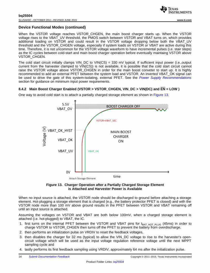
8.4.2 Main Boost Charger Enabled (VSTOR > VSTOR_CHGEN, VIN_DC > VIN(DC) and EN = LOW )One way to avoid cold start is to attach a partially charged storage element as shown in Figure 13.
Figure 13. Charger Operation after a Partially Charged Storage Elementis Attached and Harvester Power is Available
When no input source is attached, the VSTOR node should be discharged to ground before attaching a storageelement. Hot-plugging a storage element that is charged (e.g., the battery protector PFET is closed) and with theVSTOR node more than 100 mV above ground results in the PFET between VSTOR and VBAT remaining offuntil an input source is attached.
Assuming the voltages on VSTOR and VBAT are both below 100mV, when a charged storage element isattached (i.e. hot-plugged) to VBAT, the IC.1. first turns on the internal PFET between the VSTOR and VBAT pins for tBAT_HOT_PLUG (45ms) in order to
charge VSTOR to VSTOR_CHGEN then turns off the PFET to prevent the battery from overdischarge,2. then performs an initialization pulse on VRDIV to reset the feedback voltages,3. then disables the charger for 32 ms (typical) to allow the VIN_DC voltage to rise to the harvester's open-
circuit voltage which will be used as the input voltage regulation reference voltage until the next MPPTsampling cycle and
4. lastly performs its first feedback sampling using VRDIV, approximately 64 ms after the initialization pulse.
14 Submit Documentation Feedback Copyright © 2011–2015, Texas Instruments Incorporated
Product Folder Links: bq25504
bq25504www.ti.com SLUSAH0C –OCTOBER 2011–REVISED JUNE 2015
Device Functional Modes (continued)If the VSTOR pin voltage remains above the internal under voltage threshold (VBAT_UV) for the additional 64 msafter the VRDIV initialization pulse (following the 45-ms PFET on time), the internal PFET turns back on and themain boost charger begins to charge the storage element assuming there is sufficient power available from theharvester at the VIN_DC pin. If VSTOR does not reach the VBAT_UV threshold, then the PFET remains off untilthe main boost charger can raise the VSTOR voltage to VBAT_UV. If a system load tied to VSTOR dischargesVSTOR below VSTOR_GEN or below VBAT_UV during the 32 ms initial MPPT reference voltage measurementor within 110 ms after hot plug, it is recommended to add an external PFET between the system load andVSTOR. An inverted VBAT_OK signal can be used to drive the gate of this system-isolating, external PFET.Otherwise, the VSTOR voltage waveform will have incremental pulses as the IC turns on and off the internalPFET controlled by VBAT_UV or cycles between cold-start and main boost charger operation.
Once VSTOR is above VSTOR_CHGEN, the main boost charger employs pulse frequency modulation (PFM)mode of control to regulate the voltage at VIN_DC close to the desired reference voltage. The reference voltageis set by the MPPT control scheme as described in the features section. Input voltage regulation is obtained bytransferring charge from the input to VSTOR only when the input voltage is higher than the voltage on pinVREF_SAMP. The current through the inductor is controlled through internal current sense circuitry. The peakcurrent in the inductor is dithered internally to up to three pre-determined levels in order to maintain highefficiency of the charger across a wide input current range. The charger transfers up to a maximum of 100 mAaverage input current (230mA typical peak inductor current). The boost charger is disabled when the voltage onVSTOR reaches the user set VBAT_OV threshold to protect the battery connected at VBAT from overcharging.In order for the battery to charge to VBAT_OV, the input power must exceed the power needed for the load onVSTOR. See the Power Supply Recommendations section for guidance on minimum input power requirements.
Steady state operation for the boost charger is shown in Figure 16. These plots highlight the inductor current, theVSTOR voltage ripple, input voltage regulation and the LBOOST switching node. The cycle-by-cycle minorswitching frequency is a function of the boost converter's inductor value, peak current limit and voltage levels oneach side of each inductor. Once the VSTOR capacitor, CSTOR, droops below a minimum value, the hystereticswitching repeats.
CAUTIONIf VIN_DC is higher than VSTOR and VSTOR is higher than VBAT_OV, the inputVIN_DC is pulled to ground through a small resistance to stop further charging of theattached battery or capacitor. It is critical that if this case is expected, the impedance ofthe source attached to VIN_DC be higher than 20 Ω and not a low impedance source.
8.4.3 Thermal ShutdownRechargeable Li-ion batteries need protection from damage due to operation at elevated temperatures. Theapplication should provide this battery protection and ensure that the ambient temperature is never elevatedgreater than the expected operational range of 85°C.
The bq25504 uses an integrated temperature sensor to monitor the junction temperature of the device. If theOT_PROG pin is tied low, then the temperature threshold for thermal protection is set to TSD_ProtL which is65°C typically. If the OT_PROG is tied high, then the temperature is set to TSD_ProtH which is 120°C typically.Once the temperature threshold is exceeded, the boost converter/charger is disabled and charging ceases. Oncethe temperature of the device drops below this threshold, the boost converter and or charger can resumeoperation. To avoid unstable operation near the overtemp threshold, a built-in hysteresis of approximately 5°Chas been implemented. Care should be taken to not over discharge the battery in this condition since the boostconverter/charger is disabled. However, if the supply voltage drops to the VBAT_UV setting, then the switchbetween VBAT and VSTOR will open and protect the battery even if the device is in thermal shutdown.
Copyright © 2011–2015, Texas Instruments Incorporated Submit Documentation Feedback 15
Product Folder Links: bq25504

bq25504SLUSAH0C –OCTOBER 2011–REVISED JUNE 2015 www.ti.com
9 Application and Implementation
NOTEInformation in the following applications sections is not part of the TI componentspecification, and TI does not warrant its accuracy or completeness. TI’s customers areresponsible for determining suitability of components for their purposes. Customers shouldvalidate and test their design implementation to confirm system functionality.
9.1 Application Information
9.1.1 Storage Element SelectionIn order for the charge management circuitry to protect the storage element from over-charging or discharging,the storage element must be connected to VBAT pin and the system load tied to the VSTOR pin. Many types ofelements can be used, such as capacitors, super capacitors or various battery chemistries. A storage elementwith 100 uF equivalent capacitance is required to filter the pulse currents of the PFM switching charger. Theequivalent capacitance of a battery can be computed as computed as:
CEQ = 2 x mAHrBAT(CHRGD) x 3600 s/Hr / VBAT(CHRGD) (6)
In order for the storage element to be able to charge VSTOR capacitor (CSTOR) within the tVB_HOT_PLUG (50 mstypical) window at hot-plug; therefore preventing the IC from entering cold start, the time constant created by thestorage element's series resistance (plus the resistance of the internal PFET switch) and equivalent capacitancemust be less than tVB_HOT_PLUG . For example, a battery's resistance can be computed as:
RBAT = VBAT / IBAT(CONTINUOUS) from the battery specifications. (7)
The storage element must be sized large enough to provide all of the system load during periods when theharvester is no longer providing power. The harvester is expected to provide at least enough power to fullycharge the storage element while the system is in low power or sleep mode. Assuming no load on VSTOR (i.e.,the system is in low power or sleep mode), the following equation estimates charge time from voltage VBAT1 toVBAT2 for given input power is:
Refer to SLUC462 for a design example that sizes the storage element.PIN × ηEST × tCHRG = 1/2 × CEQ X (VBAT22 - VBAT12) (8)
Note that if there are large load transients or the storage element has significant impedance then it may benecessary to increase the CSTOR capacitor from the 4.7uF minimum or add additional capacitance to VBAT inorder to prevent a droop in the VSTOR voltage. See below for guidance on sizing capacitors.
9.1.2 Inductor SelectionThe boost charger needs an appropriately sized inductor for proper operation. The inductor's saturation currentshould be at least 25% higher than the expected peak inductor currents recommended below if system loadtransients on VSTOR are expected. Since this device uses hysteretic control, the boost charger is considerednaturally stable systems (single order transfer function).
For the boost charger to operate properly, an inductor of appropriate value must be connected betweenLBOOST, pin 20, and VIN_DC, pin 2. The boost charger internal control circuitry is designed to control theswitching behavior with a nominal inductance of 22 µH ± 20%. The inductor must have a peak current capabilityof > 300 mA with a low series resistance (DCR) to maintain high efficiency.
A list of inductors recommended for this device is shown in Table 1.
Table 1. Recommended InductorsInductance (µH) Dimensions (mm) Part Number Manufacturer (1)
22 4.0x4.0x1.7 LPS4018-223M Coilcraft22 3.8x3.8x1.65 744031220 Wurth22 2.8x2.8x2.8 744025220 Wurth
(1) See WHAT? concerning recommended third-party products.
16 Submit Documentation Feedback Copyright © 2011–2015, Texas Instruments Incorporated
Product Folder Links: bq25504

500 mA 50 sCSTOR 10.5 F
(4.2 V 1.8 V)
´ m³ = m
-
bq25504www.ti.com SLUSAH0C –OCTOBER 2011–REVISED JUNE 2015
9.1.3 Capacitor SelectionIn general, all the capacitors need to be low leakage. Any leakage the capacitors have will reduce efficiency,increase the quiescent current and diminish the effectiveness of the IC for energy harvesting.
9.1.3.1 VREF_SAMP CapacitanceThe MPPT operation depends on the sampled value of the open circuit voltage and the input regulation followsthe voltage stored on the CREF capacitor. This capacitor is sensitive to leakage since the holding period isaround 16 seconds. As the capacitor voltage drops due to any leakage, the input regulation voltage also dropspreventing proper operation from extraction the maximum power from the input source. Therefore, it isrecommended that the capacitor be an X7R or COG low leakage capacitor.
9.1.3.2 VIN_DC CapacitanceEnergy from the energy harvester input source is initially stored on a capacitor, CIN, connected to VIN_DC, pin2, and VSS, pin 1. For energy harvesters which have a source impedance which is dominated by a capacitivebehavior, the value of the harvester capacitor should scaled according to the value of the output capacitance ofthe energy source, but a minimum value of 4.7 µF is recommended.
9.1.3.3 VSTOR CapacitanceOperation of the bq25504 requires two capacitors to be connected between VSTOR, pin 15, and VSS, pin 1. Ahigh frequency bypass capacitor of at 0.1 µF should be placed as close as possible between VSTOR and VSS.In addition, a low ESR capacitor of at least 4.7 µF should be connected in parallel.
9.1.3.4 Additional Capacitance on VSTOR or VBATIf there are large, fast system load transients and/or the storage element has high resistance, then the CSTORcapacitors may momentarily discharge below the VBAT_UV threshold in response to the transient. This causesthe bq25504 to turn off the PFET switch between VSTOR and VBAT and turn on the boost charger. The CSTORcapacitors may further discharge below the VSTOR_CHGEN threshold and cause the bq25504 to enter ColdStart. For instance, some Li-ion batteries or thin-film batteries may not have the current capacity to meet thesurge current requirements of an attached low power radio. To prevent VSTOR from drooping, either increasingthe CSTOR capacitance or adding additional capacitance in parallel with the storage element is recommended.For example, if boost charger is configured to charge the storage element to 4.2 V and a 500 mA load transientof 50 µs duration infrequently occurs, then, solving I = C x dv/dt for CSTOR gives:
(9)
Note that increasing CSTOR is the recommended solution but will cause the boost charger to operate in the lessefficient cold start mode for a longer period at startup compared to using CSTOR = 4.7 µF. If longer cold start runtimes are not acceptable, then place the additional capacitance in parallel with the storage element.
For a recommended list of standard components, see the EVM User’s Guide (SLUUAA8).
Copyright © 2011–2015, Texas Instruments Incorporated Submit Documentation Feedback 17
Product Folder Links: bq25504

OVOV1
RSUM VBIAS3 3 10 M 1.25 VR 5.95 M 5.90 M closest 1% value then
2 VBAT _ OV 2 3.15 V
´ W ´= ´ ´ = W ® W
1
2
4
3
5 6 7 8
9
10
11
12
16 15 14 13`CHVR
LBSTCSTOR
VSTOR
VBAT_OK
bq25504
Solar
Cell
+
-
ROC1
ROC2
CREF
ROV2
ROK1
ROK2
ROK3
Battery(>100µF)
VSS
VIN_DC
AVSS
VOC_SAMP
VREF_SAMP
OT_PROG VBAT_OV VRDIV VBAT_UV
LBST VSTOR VBAT VSS
OK_HYST
OK_PROG
VBAT_OK
4.42 MΩ
1.43MΩ
4.22 MΩ
4.02MΩ
4.42 MΩ
15.62MΩ
0.01µF
4.7 µF(min)
22µH
4.7µF
RUV24.42 MΩ
RUV15.60 MΩ
ROV15.90MΩ
CBYP(1) (2)
bq25504SLUSAH0C –OCTOBER 2011–REVISED JUNE 2015 www.ti.com
9.2 Typical Applications
9.2.1 Solar Application Circuit
(1) Place close as possible to IC pin 15 (VSTOR) and pin 13 (VSS)(2) See the Capacitor Selection section for guidance on sizing CSTOR
Figure 14. Typical Solar Application Circuit
9.2.1.1 Design RequirementsThe desired voltage levels are VBAT_OV = 3.15 V, VBAT_UV = 2.20 V, VBAT_OK = 2.44 V, VBAT_OK_HYST =2.80 V and MPP (VOC) = 78% which is typical for solar panels. There are no large load transients expected. TheIC must stop charging if its junction temperature is above 65°C. The simulated solar panel open circuit voltage is1.0 V.
9.2.1.2 Detailed Design ProcedureThe recommended L1 = 22 µH, CBYP = 0.01 µF and low leakage CREF = 10 nF are selected. In order to ensurethe fastest recovery of the harvester output voltage to the MPPT level following power extraction, the minimumrecommended CIN = 4.7 µF is selected. Because no large system load transients are expected and to ensurefast charge time during cold start, the minimum recommended CSTOR = 4.7 µF. To stop charging when the ICjunction temperature is above 65°C, the OT_PROG pin is tied to ground.• With VBAT_UV < VBAT_OV ≤ 5.5 V, to size the VBAT_OV resistors, first choose RSUMOV = ROV1 + ROV2 =
10 MΩ then solve Equation 3 for
(10)• ROV2 = RSUMOV - ROV1 = 10 MΩ - 5.95 MΩ = 4.05 MΩ → 4.02 MΩ resulting in VBAT_OV = 3.15 V
18 Submit Documentation Feedback Copyright © 2011–2015, Texas Instruments Incorporated
Product Folder Links: bq25504

( )OC2 OC
VREF _ SAMPR RSUM 1 20 M 1 0.78 4.4 M closest 1% resistors
VIN_DC(OC)
æ ö= ´ - = W - = Wç ÷
è ø
OC1 OCR RSUM 0.78 20 M 15.6 M , thenVIN_DC(OC)
VREF _ SAMPæ ö= ´ = ´ W = Wç ÷
è ø
OK2 OK1
2.45 VR 1 R 1 4.24
VBIAS 1.2
VBAT _ O
5 V
K _PROGM 4.07 M , then
æ ö æ ö= - ´ = - ´ç ÷ ç ÷
è øW = W
è ø
KOK1
O 1.25 VR 10 M 4.46
VBAT _ OK _HYST 2.8
VBIAS RSUMM 4.42 M closest 1% resistor then
V
æ ö= = ´ W =ç ÷ W W
ø®
è
´
UVUV1
UV
RSUM VBIAS 10 M 1.25 VR 5.68 M 5.60 M closest 1% value then
VBAT 2.2 V
´ W ´= = = W ® W
bq25504www.ti.com SLUSAH0C –OCTOBER 2011–REVISED JUNE 2015
Typical Applications (continued)• To size the VBAT_UV resistors, first choose RSUMUV = RUV1 + RUV2 = 10 MΩ then solve Equation 2 for
(11)• RUV2 = RSUMUV - RUV1 = 10 MΩ - 5.60 MΩ = 4.4 MΩ → 4.42 MΩ closest 1% resistor resulting in
VBAT_UV = 2.2 V.• With VBAT_OV ≥ VBAT_OK_HYST > VBAT_OK ≥ VBAT_UV, to size the VBAT_OK and VBAT_OK_HYST
resistors,first choose RSUMOK = ROK1 + ROK2 + ROK3 = 10 MΩ then solve Equation 4 and Equation 5 for
(12)
(13)• ROK3 = RSUMOK - ROK1 - ROK2 = 10 MΩ - 4.42 MΩ - 4.22 MΩ = 1.36 MΩ → 1.43 MΩ to give
VBAT_OK = 2.44 V and VBAT_OK_HYST = 2.85 V.• Keeping in mind that VREF_SAMP stores the MPP voltage for the harvester, first choose RSUMOC = ROC1 +
ROC2 = 20 MΩ then solve Equation 1 for
(14)
(15)• SLURAQ1 provides help on sizing and selecting the resistors.
9.2.1.3 Application Curves
VINDC = sourcemeter with VSOURCE = 1.0 V and compliance of VIN_DC = sourcemeter with VSOURCE = 1 V and compliance of2.75 mA 10.5 mAVBAT connected to 0.1 F depleted supercap VBAT = 0.1 F supercapNo resistance load on VSTOR VSTOR = 2 kΩ resistive load
Figure 15. Startup into Depleted Storage Element Figure 16. Boost Charger Operational Waveforms
Copyright © 2011–2015, Texas Instruments Incorporated Submit Documentation Feedback 19
Product Folder Links: bq25504

bq25504SLUSAH0C –OCTOBER 2011–REVISED JUNE 2015 www.ti.com
Typical Applications (continued)
VIN_DC = sourcemeter with VSOURCE = 1 V and compliance of VIN_DC = sourcemeter with VSOURCE = 1 V and compliance of10.5 mA 10.5 mAVBAT = 0.1 F supercap VBAT = sourcemeter with VSOURCE = 2.8V and compliance
of 1AVSTOR = open to 500 Ω to open resistive load (IL = load currentIL = inductor currenton VSTOR)
Figure 17. 5 mA Load Transient on VSTOR Figure 18. MPPT Operation
VIN_DC = sourcemeter with VSOURCE = 1 V and compliance of VIN_DC = sourcemeter with VSOURCE = 1 V and compliance of10.5 mA 2.75 mAVBAT = sourcemeter with VSOURCE = 2.8 V and compliance No storage element on VBATof 1A VSTOR artificially ramped from 0V to 3.15 V to 0 V using a
power amp driven by a function generator
Figure 20. VBAT_OK OperationFigure 19. VRDIV Operation
20 Submit Documentation Feedback Copyright © 2011–2015, Texas Instruments Incorporated
Product Folder Links: bq25504

Thermo electric
generator
1
2
4
3
5 6 7 8
9
10
11
12
16 15 14 13`CHVR
LBST
VSTOR
VBAT_OK
bq25504
ROC1
ROC2
CREF
ROV2
ROK1
ROK2
ROK3
Battery(>100µF)
VSS
VIN_DC
AVSS
VOC_SAMP
VREF _SAMP
OT_PROG VBAT_OV VRDIV VBAT_UV
LBST VSTOR VBAT VSS
OK_HYST
OK_PROG
VBAT_OK
3.32 MΩ
542kΩ
6.12 MΩ
5.62MΩ
10 MΩ
10 MΩ
0.01µF
22µH
4.7µF
RUV26.12MΩ
RUV13.83MΩ
ROV14.42MΩ
VSTOR
CSTOR4.7 µF(min)
CBYP(1) (2)
bq25504www.ti.com SLUSAH0C –OCTOBER 2011–REVISED JUNE 2015
Typical Applications (continued)9.2.2 TEG Application Circuit
(1) Place close as possible to IC pin 15 (VSTOR) and pin 13 (VSS)(2) See the Capacitor Selection section for guidance on sizing CSTOR
Figure 21. Typical TEG Application Circuit
9.2.2.1 Design RequirementsThe desired voltage levels are VBAT_OV = 4.25 V, VBAT_UV = 3.20 V, VBAT_OK = 3.55 V, VBAT_OK_HYST =3.76 V and MPP (VOC) = 50% which is typical for TEG harvesters. The IC must stop charging if its junctiontemperature is above 120°C. The simulated TEG open circuit voltage is 1.0 V.
9.2.2.2 Detailed Design ProcedureThe recommended L1 = 22 µH, CBYP = 0.01 µF and low leakage CREF = 10 nF are selected. In order to ensurethe fastest recovery of the harvester output voltage to the MPPT level following power extraction, the minimumrecommended CIN = 4.7 µF is selected. Because no large system load transients are expected and to ensurefast charge time during cold start, the minimum recommended CSTOR = 4.7 µF. To stop charging when the ICjunction temperature is above 120°C, the OT_PROG pin is tied to VSTOR.
Referring back to the procedure in Detailed Design Procedure or using the spreadsheet calculator at SLURAQ1gives the following values:• ROV1 = 4.42 MΩ, ROV2 = 5.49 MΩ resulting in VBAT_OV = 4.26 V due to rounding to the nearest 1% resistor.• RUV1 = 3.83 MΩ, RUV2 = 6.04 MΩ resulting in VBAT_UV = 3.22 V due to rounding to the nearest 1% resistor• ROK1 = 3.32 MΩ, ROK2 = 6.04 MΩ, ROK3 = 0.536 MΩ resulting in VBAT_OK = 3.52 V and
VBAT_OK_HYST = 3.73 V after rounding.• ROC1 = 10 MΩ and ROC2 = 10 MΩ gives 50% MPP voltage.
Copyright © 2011–2015, Texas Instruments Incorporated Submit Documentation Feedback 21
Product Folder Links: bq25504

bq25504SLUSAH0C –OCTOBER 2011–REVISED JUNE 2015 www.ti.com
Typical Applications (continued)9.2.2.3 Application Curves
VINDC = sourcemeter with VSOURCE = 2.0 V and compliance VIN_DC = sourcemeter with VSOURCE = 2.0 V and compliance of100 mAof 1 mAVBAT connected to LiIon batteryVBAT connected to LiIon batteryVSTOR = 100 kΩ resistive load (IL = inductor current)VSTOR = 50 kΩ resistor
Figure 23. Boost Charger Operational WaveformsFigure 22. Startup by Attaching Charged Storage Element
VIN_DC = sourcemeter with VSOURCE = 2.0 V and compliance of VIN_DC = sourcemeter with VSOURCE = 2.0 V and compliance of1 mA 1 mAVBAT connected to LiIon battery VBAT connected to LiIon batteryVSTOR = open to 50Ω to open resistive load (IL = load current IL = inductor currenton VSTOR)
Figure 24. 50 mA Load Transient on VSTOR Figure 25. MPPT Operation
VIN_DC = sourcemeter with VSOURCE = 2.0 V and compliance of VIN_DC = sourcemeter with VSOURCE = 2.0 V and compliance of1 mA 1 mAVBAT connected to LiIon battery No storage element on VBAT
VSTOR artificially ramped from 0V to 4.25V to 0V using a poweramp driven by a function generator
Figure 27. VBAT_OK OperationFigure 26. VRDIV Operation
22 Submit Documentation Feedback Copyright © 2011–2015, Texas Instruments Incorporated
Product Folder Links: bq25504

1
2
4
3
5 6 7 8
9
10
11
12
16 15 14 13`CHVR
LBST
VSTOR
VBAT_OK
bq25504VSTOR
ROV2
ROK1
ROK2
ROK3
VSS
VIN_DC
AVSS
VOC_SAMP
VREF _SAMP
OT_PROG VBAT_OV VRDIV VBAT_UV
LBST VSTOR VBAT VSS
OK_HYST
OK_PROG
VBAT_OK
22µH
4.7µF
ROV1
CSTORCBYP(1) (2)
Primary Battery orother Low Z source
VSTOR
bq25504www.ti.com SLUSAH0C –OCTOBER 2011–REVISED JUNE 2015
Typical Applications (continued)9.2.3 MPPT Disabled, Low Impedance Source Application Circuit
(1) Place close as possible to IC pin 15 (VSTOR) and pin 13 (VSS)(2) See the Capacitor Selection section for guidance on sizing CSTOR
Figure 28. Typical MPPT Disabled Application Circuit(Low Iq Boost Converter from Low Impedance Source)
9.2.3.1 Design RequirementsThe input source is a low impedance 1.2 V battery therefore MPPT is not needed. The output will be a low ESRcapacitor therefore VSTOR can be tied to VBAT and VBAT_UV is not needed. The desired voltage levels areVBAT_OV = 3.30 V, VBAT_OK = 2.80 V, VBAT_OK_HYST = 3.10 V, and MPPT disabled. The IC must stopcharging if its junction temperature is above 65°C. Load transients are expected.
9.2.3.2 Detailed Design ProcedureThe recommended L1 = 22 µH, CBYP = 0.01 µF and low leakage CREF = 10 nF are selected. The minimumrecommended CIN = 4.7 µF is selected. To prevent VSTOR from drooping during system load transients,CSTOR is set to 100 µF. To disable the sampling for MPPT, the VOC_SAMP pin is tied to VSTOR. To disablethe input voltage regulation circuit, the VREF_SAMP pin is tied to GND. Since the VBAT_UV function is notneeded, the VBAT_UV can be tied to VSTOR. To stop charging when the IC junction temperature is above 65°C,the OT_PROG pin is tied to GND.
Referring back to the procedure in Detailed Design Procedure or using the spreadsheet calculator at SLURAQ1gives the following values:• ROV1 = 5.62 MΩ, ROV2 = 4.22 MΩ resulting in VBAT_OV = 3.28 V due to rounding to the nearest 1% resistor.• ROK1 = 4.12 MΩ, ROK2 = 5.11 MΩ, ROK3 = 0.976 MΩ resulting in VBAT_OK = 2.80 V and VBAT_OK_HYST =
3.10 V after rounding.
Copyright © 2011–2015, Texas Instruments Incorporated Submit Documentation Feedback 23
Product Folder Links: bq25504

bq25504SLUSAH0C –OCTOBER 2011–REVISED JUNE 2015 www.ti.com
Typical Applications (continued)9.2.3.3 Application Curves
VIN_DC = low impedance voltage source = 1.5 V VIN_DC = low impedance voltage source = 1.5 VVBAT = VSTOR = 100 µF VBAT = VSTOR = 100 µFVSTOR = 500 Ω resistor VSTOR = 330 Ω resistive load (IL = inductor current)
Figure 29. Startup Figure 30. Boost Charger Operational Waveforms
VIN_DC = low impedance voltage source = 1.5 V )VIN_DC = low impedance voltage source = 1.5 VVBAT = VSTOR = 100 µFVBAT = VSTOR = 100 µFVSTOR = open to 75 Ω to open resistive load (IL = load current
on VSTOR
Figure 32. VRDIV OperationFigure 31. 40 mA Load Transient on VSTOR
VIN_DC = low impedance voltage source = 1.5 VVBAT = VSTOR = 100 µF
VSTOR artificially ramped from 0 V to 3.3 V to 0 V using a power amp driven by a function generator
Figure 33. VBAT_OK Operation
24 Submit Documentation Feedback Copyright © 2011–2015, Texas Instruments Incorporated
Product Folder Links: bq25504

( )2
EST @ VBAT _ OV
VBAT _ OVPIN PLOAD VBAT _ OV I STR _ELM_LEAK
RSTOR(AVG)´ h > = + ´ -
( )( )
2
@1.8V
1.8VI STR _ELM_LEAK 1.8V
RSTOR(CS)PIN PIN(CS) VIN(CS) IIN(CS)
0.05
- ´ +
> = ´ >
bq25504www.ti.com SLUSAH0C –OCTOBER 2011–REVISED JUNE 2015
10 Power Supply RecommendationsThe energy harvesting source (e.g., solar panel, TEG, vibration element) must provide a minimum level of powerfor the IC to operate as designed. The IC's minimum input power required to exit cold start can be estimated as:
(16)
where [email protected] is the storage element leakage current at 1.8V and
RSTOR(CS) is the equivalent resistive load on VSTOR during cold start and 0.05 is an estimate of the worstcase efficiency of the cold start circuit.
Once the IC is out of cold start and the system load has been activated (e.g., using the VBAT_OK signal), theenergy harvesting element must provide the main boost charger with at least enough power to meet the averagesystem load. Assuming RSTOR(AVG) represents the average resistive load on VSTOR, the simplified equationbelow gives an estimate of the IC's minimum input power needed during system operation:
(17)
where ηEST can be derived from the datasheet efficiency curves for the given input voltage and current andVBAT_OV. The simplified equation above assumes that, while the harvester is still providing power, the systemgoes into low power or sleep mode long enough to charge the storage element so that it can power the systemwhen the harvester eventually is down. Refer to spreadsheet SLUC462 for a design example that sizes theenergy harvester.
11 Layout
11.1 Layout GuidelinesAs for all switching power supplies, the PCB layout is an important step in the design, especially at high peakcurrents and high switching frequencies. If the layout is not carefully done, the boost charger could show stabilityproblems as well as EMI problems. Therefore, use wide and short traces for the main current path and for thepower ground paths. The input and output capacitors as well as the inductors should be placed as close aspossible to the IC. For the boost charger, first priority are the output capacitors, including the 0.1 uF bypasscapacitor (CBYP), followed by CSTOR, which should be placed as close as possible between VSTOR, pin 15,and VSS, pin 1 or 13. Next, the input capacitor, CIN, should be placed as close as possible between VIN_DC,pin 2, and VSS, pin 1. Last in priority is the boost charger inductor, L1, which should be placed close toLBOOST, pin 16, and VIN_DC, pin 2 if possible. It is best to use vias and bottom traces for connecting theinductor to its respective pins instead of the capacitors.
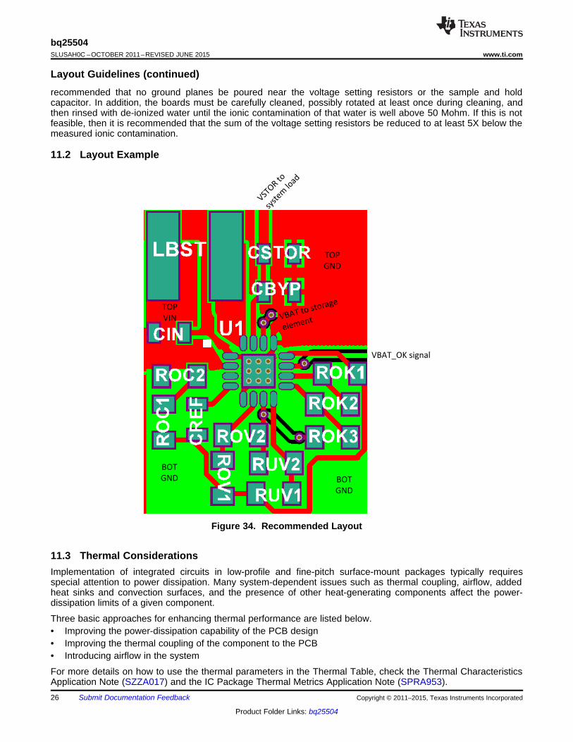
To minimize noise pickup by the high impedance voltage setting nodes (VBAT_OV, VBAT_UV, OK_PROG,OK_HYST), the external resistors should be placed so that the traces connecting the midpoints of each divider totheir respective pins are as short as possible. When laying out the non-power ground return paths (e.g. fromresistors and CREF), it is recommended to use short traces as well, separated from the power ground traces andconnected to AVSS pin 12. This avoids ground shift problems, which can occur due to superimposition of powerground current and control ground current. The PowerPad should not be used as a power ground return path.
The remaining pins are digital signals with minimal layout restrictions. See Figure 34 for an example layout.
In order to maximize efficiency at light load, the use of voltage level setting resistors > 1 MΩ is recommended. Inaddition, the sample and hold circuit output capacitor on VREF_SAMP must hold the voltage for 16 s. Duringboard assembly, contaminants such as solder flux and even some board cleaning agents can leave residue thatmay form parasitic resistors across the physical resistors/capacitors and/or from one end of a resistor/capacitorto ground, especially in humid, fast airflow environments. This can result in the voltage regulation and thresholdlevels changing significantly from those expected per the installed components. Therefore, it is highly
Copyright © 2011–2015, Texas Instruments Incorporated Submit Documentation Feedback 25
Product Folder Links: bq25504
VBAT_OK signal
TOP
GND
BOT
GND BOT
GND
TOP
VIN VBAT to storage
element
VSTO
R to
syst
em lo
ad
bq25504SLUSAH0C –OCTOBER 2011–REVISED JUNE 2015 www.ti.com
Layout Guidelines (continued)recommended that no ground planes be poured near the voltage setting resistors or the sample and holdcapacitor. In addition, the boards must be carefully cleaned, possibly rotated at least once during cleaning, andthen rinsed with de-ionized water until the ionic contamination of that water is well above 50 Mohm. If this is notfeasible, then it is recommended that the sum of the voltage setting resistors be reduced to at least 5X below themeasured ionic contamination.
11.2 Layout Example
Figure 34. Recommended Layout
11.3 Thermal ConsiderationsImplementation of integrated circuits in low-profile and fine-pitch surface-mount packages typically requiresspecial attention to power dissipation. Many system-dependent issues such as thermal coupling, airflow, addedheat sinks and convection surfaces, and the presence of other heat-generating components affect the power-dissipation limits of a given component.
Three basic approaches for enhancing thermal performance are listed below.• Improving the power-dissipation capability of the PCB design• Improving the thermal coupling of the component to the PCB• Introducing airflow in the system
For more details on how to use the thermal parameters in the Thermal Table, check the Thermal CharacteristicsApplication Note (SZZA017) and the IC Package Thermal Metrics Application Note (SPRA953).26 Submit Documentation Feedback Copyright © 2011–2015, Texas Instruments Incorporated
Product Folder Links: bq25504

bq25504www.ti.com SLUSAH0C –OCTOBER 2011–REVISED JUNE 2015
12 Device and Documentation Support
12.1 Device Support
12.1.1 Third-Party Products DisclaimerTI'S PUBLICATION OF INFORMATION REGARDING THIRD-PARTY PRODUCTS OR SERVICES DOES NOTCONSTITUTE AN ENDORSEMENT REGARDING THE SUITABILITY OF SUCH PRODUCTS OR SERVICESOR A WARRANTY, REPRESENTATION OR ENDORSEMENT OF SUCH PRODUCTS OR SERVICES, EITHERALONE OR IN COMBINATION WITH ANY TI PRODUCT OR SERVICE.
12.1.2 Zip Files• http://www.ti.com/lit/zip/SLUC484• http://www.ti.com/lit/zip/SLURAQ1• http://www.ti.com/lit/zip/SLUC462
12.2 Documentation Support
12.2.1 Related DocumentationFor related documentation see the following:• EVM User’s Guide, SLUUAA8• Thermal Characteristics Application Note, SZZA017• IC Package Thermal Metrics Application Note, SPRA953
12.3 TrademarksAll trademarks are the property of their respective owners.
12.4 Electrostatic Discharge CautionThese devices have limited built-in ESD protection. The leads should be shorted together or the device placed in conductive foamduring storage or handling to prevent electrostatic damage to the MOS gates.
12.5 GlossarySLYZ022 — TI Glossary.
This glossary lists and explains terms, acronyms, and definitions.
13 Mechanical, Packaging, and Orderable InformationThe following pages include mechanical, packaging, and orderable information. This information is the mostcurrent data available for the designated devices. This data is subject to change without notice and revision ofthis document. For browser-based versions of this data sheet, refer to the left-hand navigation.
Copyright © 2011–2015, Texas Instruments Incorporated Submit Documentation Feedback 27
Product Folder Links: bq25504
PACKAGE OPTION ADDENDUM
www.ti.com 11-Aug-2017
Addendum-Page 1
PACKAGING INFORMATION
Orderable Device Status(1)
Package Type PackageDrawing
Pins PackageQty
Eco Plan(2)
Lead/Ball Finish(6)
MSL Peak Temp(3)
Op Temp (°C) Device Marking(4/5)
Samples
BQ25504RGTR ACTIVE VQFN RGT 16 3000 Green (RoHS& no Sb/Br)
CU NIPDAU Level-2-260C-1 YEAR -40 to 85 B5504
BQ25504RGTT ACTIVE VQFN RGT 16 250 Green (RoHS& no Sb/Br)
CU NIPDAU Level-2-260C-1 YEAR -40 to 85 B5504
(1) The marketing status values are defined as follows:ACTIVE: Product device recommended for new designs.LIFEBUY: TI has announced that the device will be discontinued, and a lifetime-buy period is in effect.NRND: Not recommended for new designs. Device is in production to support existing customers, but TI does not recommend using this part in a new design.PREVIEW: Device has been announced but is not in production. Samples may or may not be available.OBSOLETE: TI has discontinued the production of the device.
(2) RoHS: TI defines "RoHS" to mean semiconductor products that are compliant with the current EU RoHS requirements for all 10 RoHS substances, including the requirement that RoHS substancedo not exceed 0.1% by weight in homogeneous materials. Where designed to be soldered at high temperatures, "RoHS" products are suitable for use in specified lead-free processes. TI mayreference these types of products as "Pb-Free".RoHS Exempt: TI defines "RoHS Exempt" to mean products that contain lead but are compliant with EU RoHS pursuant to a specific EU RoHS exemption.Green: TI defines "Green" to mean the content of Chlorine (Cl) and Bromine (Br) based flame retardants meet JS709B low halogen requirements of <=1000ppm threshold. Antimony trioxide basedflame retardants must also meet the <=1000ppm threshold requirement.
(3) MSL, Peak Temp. - The Moisture Sensitivity Level rating according to the JEDEC industry standard classifications, and peak solder temperature.
(4) There may be additional marking, which relates to the logo, the lot trace code information, or the environmental category on the device.
(5) Multiple Device Markings will be inside parentheses. Only one Device Marking contained in parentheses and separated by a "~" will appear on a device. If a line is indented then it is a continuationof the previous line and the two combined represent the entire Device Marking for that device.
(6) Lead/Ball Finish - Orderable Devices may have multiple material finish options. Finish options are separated by a vertical ruled line. Lead/Ball Finish values may wrap to two lines if the finishvalue exceeds the maximum column width.
Important Information and Disclaimer:The information provided on this page represents TI's knowledge and belief as of the date that it is provided. TI bases its knowledge and belief on informationprovided by third parties, and makes no representation or warranty as to the accuracy of such information. Efforts are underway to better integrate information from third parties. TI has taken andcontinues to take reasonable steps to provide representative and accurate information but may not have conducted destructive testing or chemical analysis on incoming materials and chemicals.TI and TI suppliers consider certain information to be proprietary, and thus CAS numbers and other limited information may not be available for release.
In no event shall TI's liability arising out of such information exceed the total purchase price of the TI part(s) at issue in this document sold by TI to Customer on an annual basis.

PACKAGE OPTION ADDENDUM
www.ti.com 11-Aug-2017
Addendum-Page 2

TAPE AND REEL INFORMATION
*All dimensions are nominal
Device PackageType
PackageDrawing
Pins SPQ ReelDiameter
(mm)
ReelWidth
W1 (mm)
A0(mm)
B0(mm)
K0(mm)
P1(mm)
W(mm)
Pin1Quadrant
BQ25504RGTR VQFN RGT 16 3000 330.0 12.4 3.3 3.3 1.1 8.0 12.0 Q2
BQ25504RGTT VQFN RGT 16 250 180.0 12.4 3.3 3.3 1.1 8.0 12.0 Q2
PACKAGE MATERIALS INFORMATION
www.ti.com 11-Aug-2017
Pack Materials-Page 1

*All dimensions are nominal
Device Package Type Package Drawing Pins SPQ Length (mm) Width (mm) Height (mm)
BQ25504RGTR VQFN RGT 16 3000 367.0 367.0 35.0
BQ25504RGTT VQFN RGT 16 250 210.0 185.0 35.0
PACKAGE MATERIALS INFORMATION
www.ti.com 11-Aug-2017
Pack Materials-Page 2


www.ti.com
PACKAGE OUTLINE
C
16X 0.300.18
1.68 0.07
16X 0.50.3
1 MAX
(0.2) TYP
0.050.00
12X 0.5
4X1.5
A 3.12.9
B
3.12.9
VQFN - 1 mm max heightRGT0016CPLASTIC QUAD FLATPACK - NO LEAD
4222419/B 11/2016
PIN 1 INDEX AREA
0.08
SEATING PLANE
1
49
12
5 8
16 13
(OPTIONAL)PIN 1 ID 0.1 C A B
0.05
EXPOSEDTHERMAL PAD
SYMM
SYMM
NOTES: 1. All linear dimensions are in millimeters. Any dimensions in parenthesis are for reference only. Dimensioning and tolerancing per ASME Y14.5M. 2. This drawing is subject to change without notice. 3. The package thermal pad must be soldered to the printed circuit board for thermal and mechanical performance.
SCALE 3.600

www.ti.com
EXAMPLE BOARD LAYOUT
0.07 MINALL AROUND
0.07 MAXALL AROUND
16X (0.24)
16X (0.6)
( 0.2) TYPVIA
12X (0.5)
(2.8)
(2.8)
(0.58)TYP
( 1.68)
(R0.05)ALL PAD CORNERS
(0.58) TYP
VQFN - 1 mm max heightRGT0016CPLASTIC QUAD FLATPACK - NO LEAD
4222419/B 11/2016
SYMM
1
4
5 8
9
12
1316
SYMM
LAND PATTERN EXAMPLESCALE:20X
NOTES: (continued) 4. This package is designed to be soldered to a thermal pad on the board. For more information, see Texas Instruments literature number SLUA271 (www.ti.com/lit/slua271).5. Vias are optional depending on application, refer to device data sheet. If any vias are implemented, refer to their locations shown on this view. It is recommended that vias under paste be filled, plugged or tented.
SOLDER MASKOPENING
METAL UNDERSOLDER MASK
SOLDER MASKDEFINED
METAL
SOLDER MASKOPENING
SOLDER MASK DETAILS
NON SOLDER MASKDEFINED
(PREFERRED)

www.ti.com
EXAMPLE STENCIL DESIGN
16X (0.6)
16X (0.24)
12X (0.5)
(2.8)
(2.8)
( 1.55)
(R0.05) TYP
VQFN - 1 mm max heightRGT0016CPLASTIC QUAD FLATPACK - NO LEAD
4222419/B 11/2016
NOTES: (continued) 6. Laser cutting apertures with trapezoidal walls and rounded corners may offer better paste release. IPC-7525 may have alternate design recommendations.
SYMM
ALL AROUNDMETAL
SOLDER PASTE EXAMPLEBASED ON 0.125 mm THICK STENCIL
EXPOSED PAD 17:
85% PRINTED SOLDER COVERAGE BY AREA UNDER PACKAGESCALE:25X
SYMM
1
4
5 8
9
12
1316
17

IMPORTANT NOTICE
Texas Instruments Incorporated (TI) reserves the right to make corrections, enhancements, improvements and other changes to itssemiconductor products and services per JESD46, latest issue, and to discontinue any product or service per JESD48, latest issue. Buyersshould obtain the latest relevant information before placing orders and should verify that such information is current and complete.TI’s published terms of sale for semiconductor products (http://www.ti.com/sc/docs/stdterms.htm) apply to the sale of packaged integratedcircuit products that TI has qualified and released to market. Additional terms may apply to the use or sale of other types of TI products andservices.Reproduction of significant portions of TI information in TI data sheets is permissible only if reproduction is without alteration and isaccompanied by all associated warranties, conditions, limitations, and notices. TI is not responsible or liable for such reproduceddocumentation. Information of third parties may be subject to additional restrictions. Resale of TI products or services with statementsdifferent from or beyond the parameters stated by TI for that product or service voids all express and any implied warranties for theassociated TI product or service and is an unfair and deceptive business practice. TI is not responsible or liable for any such statements.Buyers and others who are developing systems that incorporate TI products (collectively, “Designers”) understand and agree that Designersremain responsible for using their independent analysis, evaluation and judgment in designing their applications and that Designers havefull and exclusive responsibility to assure the safety of Designers' applications and compliance of their applications (and of all TI productsused in or for Designers’ applications) with all applicable regulations, laws and other applicable requirements. Designer represents that, withrespect to their applications, Designer has all the necessary expertise to create and implement safeguards that (1) anticipate dangerousconsequences of failures, (2) monitor failures and their consequences, and (3) lessen the likelihood of failures that might cause harm andtake appropriate actions. Designer agrees that prior to using or distributing any applications that include TI products, Designer willthoroughly test such applications and the functionality of such TI products as used in such applications.TI’s provision of technical, application or other design advice, quality characterization, reliability data or other services or information,including, but not limited to, reference designs and materials relating to evaluation modules, (collectively, “TI Resources”) are intended toassist designers who are developing applications that incorporate TI products; by downloading, accessing or using TI Resources in anyway, Designer (individually or, if Designer is acting on behalf of a company, Designer’s company) agrees to use any particular TI Resourcesolely for this purpose and subject to the terms of this Notice.TI’s provision of TI Resources does not expand or otherwise alter TI’s applicable published warranties or warranty disclaimers for TIproducts, and no additional obligations or liabilities arise from TI providing such TI Resources. TI reserves the right to make corrections,enhancements, improvements and other changes to its TI Resources. TI has not conducted any testing other than that specificallydescribed in the published documentation for a particular TI Resource.Designer is authorized to use, copy and modify any individual TI Resource only in connection with the development of applications thatinclude the TI product(s) identified in such TI Resource. NO OTHER LICENSE, EXPRESS OR IMPLIED, BY ESTOPPEL OR OTHERWISETO ANY OTHER TI INTELLECTUAL PROPERTY RIGHT, AND NO LICENSE TO ANY TECHNOLOGY OR INTELLECTUAL PROPERTYRIGHT OF TI OR ANY THIRD PARTY IS GRANTED HEREIN, including but not limited to any patent right, copyright, mask work right, orother intellectual property right relating to any combination, machine, or process in which TI products or services are used. Informationregarding or referencing third-party products or services does not constitute a license to use such products or services, or a warranty orendorsement thereof. Use of TI Resources may require a license from a third party under the patents or other intellectual property of thethird party, or a license from TI under the patents or other intellectual property of TI.TI RESOURCES ARE PROVIDED “AS IS” AND WITH ALL FAULTS. TI DISCLAIMS ALL OTHER WARRANTIES ORREPRESENTATIONS, EXPRESS OR IMPLIED, REGARDING RESOURCES OR USE THEREOF, INCLUDING BUT NOT LIMITED TOACCURACY OR COMPLETENESS, TITLE, ANY EPIDEMIC FAILURE WARRANTY AND ANY IMPLIED WARRANTIES OFMERCHANTABILITY, FITNESS FOR A PARTICULAR PURPOSE, AND NON-INFRINGEMENT OF ANY THIRD PARTY INTELLECTUALPROPERTY RIGHTS. TI SHALL NOT BE LIABLE FOR AND SHALL NOT DEFEND OR INDEMNIFY DESIGNER AGAINST ANY CLAIM,INCLUDING BUT NOT LIMITED TO ANY INFRINGEMENT CLAIM THAT RELATES TO OR IS BASED ON ANY COMBINATION OFPRODUCTS EVEN IF DESCRIBED IN TI RESOURCES OR OTHERWISE. IN NO EVENT SHALL TI BE LIABLE FOR ANY ACTUAL,DIRECT, SPECIAL, COLLATERAL, INDIRECT, PUNITIVE, INCIDENTAL, CONSEQUENTIAL OR EXEMPLARY DAMAGES INCONNECTION WITH OR ARISING OUT OF TI RESOURCES OR USE THEREOF, AND REGARDLESS OF WHETHER TI HAS BEENADVISED OF THE POSSIBILITY OF SUCH DAMAGES.Unless TI has explicitly designated an individual product as meeting the requirements of a particular industry standard (e.g., ISO/TS 16949and ISO 26262), TI is not responsible for any failure to meet such industry standard requirements.Where TI specifically promotes products as facilitating functional safety or as compliant with industry functional safety standards, suchproducts are intended to help enable customers to design and create their own applications that meet applicable functional safety standardsand requirements. Using products in an application does not by itself establish any safety features in the application. Designers mustensure compliance with safety-related requirements and standards applicable to their applications. Designer may not use any TI products inlife-critical medical equipment unless authorized officers of the parties have executed a special contract specifically governing such use.Life-critical medical equipment is medical equipment where failure of such equipment would cause serious bodily injury or death (e.g., lifesupport, pacemakers, defibrillators, heart pumps, neurostimulators, and implantables). Such equipment includes, without limitation, allmedical devices identified by the U.S. Food and Drug Administration as Class III devices and equivalent classifications outside the U.S.TI may expressly designate certain products as completing a particular qualification (e.g., Q100, Military Grade, or Enhanced Product).Designers agree that it has the necessary expertise to select the product with the appropriate qualification designation for their applicationsand that proper product selection is at Designers’ own risk. Designers are solely responsible for compliance with all legal and regulatoryrequirements in connection with such selection.Designer will fully indemnify TI and its representatives against any damages, costs, losses, and/or liabilities arising out of Designer’s non-compliance with the terms and provisions of this Notice.
Mailing Address: Texas Instruments, Post Office Box 655303, Dallas, Texas 75265Copyright © 2017, Texas Instruments Incorporated