Ultra-low-power 32-bit MCU ARM®-based Cortex®-M0+, up to...
130
This is information on a product in full production. March 2016 DocID025844 Rev 6 1/131 STM32L053C6 STM32L053C8 STM32L053R6 STM32L053R8 Ultra-low-power 32-bit MCU ARM ® -based Cortex ® -M0+, up to 64KB Flash, 8KB SRAM, 2KB EEPROM, LCD, USB, ADC, DAC Datasheet - production data Features Ultra-low-power platform – 1.65 V to 3.6 V power supply – -40 to 125 °C temperature range – 0.27 μA Standby mode (2 wakeup pins) – 0.4 μA Stop mode (16 wakeup lines) – 0.8 μA Stop mode + RTC + 8 KB RAM retention – 88 μA/MHz in Run mode – 3.5 μs wakeup time (from RAM) – 5 μs wakeup time (from Flash memory) Core: ARM ® 32-bit Cortex ® -M0+ with MPU – From 32 kHz up to 32 MHz max. – 0.95 DMIPS/MHz Reset and supply management – Ultra-safe, low-power BOR (brownout reset) with 5 selectable thresholds – Ultra-low-power POR/PDR – Programmable voltage detector (PVD) Clock sources – 1 to 25 MHz crystal oscillator – 32 kHz oscillator for RTC with calibration – High speed internal 16 MHz factory-trimmed RC (+/- 1%) – Internal low-power 37 kHz RC – Internal multispeed low-power 65 kHz to 4.2 MHz RC – PLL for CPU clock Pre-programmed bootloader – USART, SPI supported Development support – Serial wire debug supported Up to 51 fast I/Os (45 I/Os 5V tolerant) Memories – Up to 64 KB Flash memory with ECC – 8KB RAM – 2 KB of data EEPROM with ECC – 20-byte backup register – Sector protection against R/W operation LCD driver for up to 8×28segments – Support contrast adjustment – Support blinking mode – Step-up converted on board Rich Analog peripherals – 12-bit ADC 1.14 Msps up to 16 channels (down to 1.65 V) – 12-bit 1 channel DAC with output buffers (down to 1.8 V) – 2x ultra-low-power comparators (window mode and wake up capability, down to 1.65 V) Up to 24 capacitive sensing channels supporting touchkey, linear and rotary touch sensors 7-channel DMA controller, supporting ADC, SPI, I2C, USART, DAC, Timers 8x peripheral communication interfaces – 1x USB 2.0 crystal-less, battery charging detection and LPM – 2x USART (ISO 7816, IrDA), 1x UART (low power) – Up to 4x SPI 16 Mbits/s – 2x I2C (SMBus/PMBus) 9x timers: 1x 16-bit with up to 4 channels, 2x 16-bit with up to 2 channels, 1x 16-bit ultra-low-power timer, 1x SysTick, 1x RTC, 1x 16-bit basic for DAC, and 2x watchdogs (independent/window) CRC calculation unit, 96-bit unique ID True RNG and firewall protection All packages are ECOPACK ® 2 LQFP64 10x10 mm LQFP48 7x7 mm TFBGA64 5x5 mm www.st.com
Transcript of Ultra-low-power 32-bit MCU ARM®-based Cortex®-M0+, up to...

This is information on a product in full production.
March 2016 DocID025844 Rev 6 1/131
STM32L053C6 STM32L053C8 STM32L053R6 STM32L053R8
Ultra-low-power 32-bit MCU ARM®-based Cortex®-M0+, up to 64KB Flash, 8KB SRAM, 2KB EEPROM, LCD, USB, ADC, DAC
Datasheet - production data
Features Ultra-low-power platform
– 1.65 V to 3.6 V power supply– -40 to 125 °C temperature range– 0.27 µA Standby mode (2 wakeup pins)– 0.4 µA Stop mode (16 wakeup lines)– 0.8 µA Stop mode + RTC + 8 KB RAM retention– 88 µA/MHz in Run mode– 3.5 µs wakeup time (from RAM)– 5 µs wakeup time (from Flash memory)
Core: ARM® 32-bit Cortex®-M0+ with MPU– From 32 kHz up to 32 MHz max. – 0.95 DMIPS/MHz
Reset and supply management– Ultra-safe, low-power BOR (brownout reset)
with 5 selectable thresholds– Ultra-low-power POR/PDR– Programmable voltage detector (PVD)
Clock sources– 1 to 25 MHz crystal oscillator– 32 kHz oscillator for RTC with calibration– High speed internal 16 MHz factory-trimmed RC
(+/- 1%)– Internal low-power 37 kHz RC– Internal multispeed low-power 65 kHz to
4.2 MHz RC– PLL for CPU clock
Pre-programmed bootloader– USART, SPI supported
Development support– Serial wire debug supported
Up to 51 fast I/Os (45 I/Os 5V tolerant)
Memories – Up to 64 KB Flash memory with ECC– 8KB RAM– 2 KB of data EEPROM with ECC– 20-byte backup register– Sector protection against R/W operation
LCD driver for up to 8×28segments– Support contrast adjustment– Support blinking mode– Step-up converted on board
Rich Analog peripherals
– 12-bit ADC 1.14 Msps up to 16 channels (down to 1.65 V)
– 12-bit 1 channel DAC with output buffers (down to 1.8 V)
– 2x ultra-low-power comparators (window mode and wake up capability, down to 1.65 V)
Up to 24 capacitive sensing channels supporting touchkey, linear and rotary touch sensors
7-channel DMA controller, supporting ADC, SPI, I2C, USART, DAC, Timers
8x peripheral communication interfaces– 1x USB 2.0 crystal-less, battery charging
detection and LPM – 2x USART (ISO 7816, IrDA), 1x UART (low
power)– Up to 4x SPI 16 Mbits/s– 2x I2C (SMBus/PMBus)
9x timers: 1x 16-bit with up to 4 channels, 2x 16-bit with up to 2 channels, 1x 16-bit ultra-low-power timer, 1x SysTick, 1x RTC, 1x 16-bit basic for DAC, and 2x watchdogs (independent/window)
CRC calculation unit, 96-bit unique ID
True RNG and firewall protection
All packages are ECOPACK®2
LQFP64 10x10 mmLQFP48 7x7 mm
TFBGA64 5x5 mm
www.st.com
Contents STM32L053x6 STM32L053x8
2/131 DocID025844 Rev 6
Contents
1 Introduction . . . . . . . . . . . . . . . . . . . . . . . . . . . . . . . . . . . . . . . . . . . . . . . . 9
2 Description . . . . . . . . . . . . . . . . . . . . . . . . . . . . . . . . . . . . . . . . . . . . . . . . 10
2.1 Device overview . . . . . . . . . . . . . . . . . . . . . . . . . . . . . . . . . . . . . . . . . . . . .11
2.2 Ultra-low-power device continuum . . . . . . . . . . . . . . . . . . . . . . . . . . . . . . 13
3 Functional overview . . . . . . . . . . . . . . . . . . . . . . . . . . . . . . . . . . . . . . . . 14
3.1 Low-power modes . . . . . . . . . . . . . . . . . . . . . . . . . . . . . . . . . . . . . . . . . . 14
3.2 Interconnect matrix . . . . . . . . . . . . . . . . . . . . . . . . . . . . . . . . . . . . . . . . . . 19
3.3 ARM® Cortex®-M0+ core with MPU . . . . . . . . . . . . . . . . . . . . . . . . . . . . 20
3.4 Reset and supply management . . . . . . . . . . . . . . . . . . . . . . . . . . . . . . . . 21
3.4.1 Power supply schemes . . . . . . . . . . . . . . . . . . . . . . . . . . . . . . . . . . . . . 21
3.4.2 Power supply supervisor . . . . . . . . . . . . . . . . . . . . . . . . . . . . . . . . . . . . 21
3.4.3 Voltage regulator . . . . . . . . . . . . . . . . . . . . . . . . . . . . . . . . . . . . . . . . . . 22
3.5 Clock management . . . . . . . . . . . . . . . . . . . . . . . . . . . . . . . . . . . . . . . . . 22
3.6 Low-power real-time clock and backup registers . . . . . . . . . . . . . . . . . . . 26
3.7 General-purpose inputs/outputs (GPIOs) . . . . . . . . . . . . . . . . . . . . . . . . . 26
3.8 Memories . . . . . . . . . . . . . . . . . . . . . . . . . . . . . . . . . . . . . . . . . . . . . . . . . 27
3.9 Boot modes . . . . . . . . . . . . . . . . . . . . . . . . . . . . . . . . . . . . . . . . . . . . . . . 27
3.10 Direct memory access (DMA) . . . . . . . . . . . . . . . . . . . . . . . . . . . . . . . . . 28
3.11 Liquid crystal display (LCD) . . . . . . . . . . . . . . . . . . . . . . . . . . . . . . . . . . . 28
3.12 Analog-to-digital converter (ADC) . . . . . . . . . . . . . . . . . . . . . . . . . . . . . . 28
3.13 Temperature sensor . . . . . . . . . . . . . . . . . . . . . . . . . . . . . . . . . . . . . . . . . 29
3.13.1 Internal voltage reference (VREFINT) . . . . . . . . . . . . . . . . . . . . . . . . . . . 29
3.13.2 VLCD voltage monitoring . . . . . . . . . . . . . . . . . . . . . . . . . . . . . . . . . . . . 30
3.14 Digital-to-analog converter (DAC) . . . . . . . . . . . . . . . . . . . . . . . . . . . . . . 30
3.15 Ultra-low-power comparators and reference voltage . . . . . . . . . . . . . . . . 30
3.16 System configuration controller . . . . . . . . . . . . . . . . . . . . . . . . . . . . . . . . 31
3.17 Touch sensing controller (TSC) . . . . . . . . . . . . . . . . . . . . . . . . . . . . . . . . 31
3.18 Timers and watchdogs . . . . . . . . . . . . . . . . . . . . . . . . . . . . . . . . . . . . . . . 32
3.18.1 General-purpose timers (TIM2, TIM21 and TIM22) . . . . . . . . . . . . . . . . 32
3.18.2 Low-power Timer (LPTIM) . . . . . . . . . . . . . . . . . . . . . . . . . . . . . . . . . . . 33
DocID025844 Rev 6 3/131
STM32L053x6 STM32L053x8 Contents
4
3.18.3 Basic timer (TIM6) . . . . . . . . . . . . . . . . . . . . . . . . . . . . . . . . . . . . . . . . . 33
3.18.4 SysTick timer . . . . . . . . . . . . . . . . . . . . . . . . . . . . . . . . . . . . . . . . . . . . . 33
3.18.5 Independent watchdog (IWDG) . . . . . . . . . . . . . . . . . . . . . . . . . . . . . . . 33
3.18.6 Window watchdog (WWDG) . . . . . . . . . . . . . . . . . . . . . . . . . . . . . . . . . 34
3.19 Communication interfaces . . . . . . . . . . . . . . . . . . . . . . . . . . . . . . . . . . . . 34
3.19.1 I2C bus . . . . . . . . . . . . . . . . . . . . . . . . . . . . . . . . . . . . . . . . . . . . . . . . . 34
3.19.2 Universal synchronous/asynchronous receiver transmitter (USART) . . 35
3.19.3 Low-power universal asynchronous receiver transmitter (LPUART) . . . 35
3.19.4 Serial peripheral interface (SPI)/Inter-integrated sound (I2S) . . . . . . . . 36
3.19.5 Universal serial bus (USB) . . . . . . . . . . . . . . . . . . . . . . . . . . . . . . . . . . . 37
3.20 Clock recovery system (CRS) . . . . . . . . . . . . . . . . . . . . . . . . . . . . . . . . . 37
3.21 Cyclic redundancy check (CRC) calculation unit . . . . . . . . . . . . . . . . . . . 37
3.22 Serial wire debug port (SW-DP) . . . . . . . . . . . . . . . . . . . . . . . . . . . . . . . . 37
4 Pin descriptions . . . . . . . . . . . . . . . . . . . . . . . . . . . . . . . . . . . . . . . . . . . 38
5 Memory mapping . . . . . . . . . . . . . . . . . . . . . . . . . . . . . . . . . . . . . . . . . . . 51
6 Electrical characteristics . . . . . . . . . . . . . . . . . . . . . . . . . . . . . . . . . . . . 52
6.1 Parameter conditions . . . . . . . . . . . . . . . . . . . . . . . . . . . . . . . . . . . . . . . . 52
6.1.1 Minimum and maximum values . . . . . . . . . . . . . . . . . . . . . . . . . . . . . . . 52
6.1.2 Typical values . . . . . . . . . . . . . . . . . . . . . . . . . . . . . . . . . . . . . . . . . . . . 52
6.1.3 Typical curves . . . . . . . . . . . . . . . . . . . . . . . . . . . . . . . . . . . . . . . . . . . . 52
6.1.4 Loading capacitor . . . . . . . . . . . . . . . . . . . . . . . . . . . . . . . . . . . . . . . . . 52
6.1.5 Pin input voltage . . . . . . . . . . . . . . . . . . . . . . . . . . . . . . . . . . . . . . . . . . 52
6.1.6 Power supply scheme . . . . . . . . . . . . . . . . . . . . . . . . . . . . . . . . . . . . . . 53
6.1.7 Optional LCD power supply scheme . . . . . . . . . . . . . . . . . . . . . . . . . . . 54
6.1.8 Current consumption measurement . . . . . . . . . . . . . . . . . . . . . . . . . . . 54
6.2 Absolute maximum ratings . . . . . . . . . . . . . . . . . . . . . . . . . . . . . . . . . . . . 55
6.3 Operating conditions . . . . . . . . . . . . . . . . . . . . . . . . . . . . . . . . . . . . . . . . 57
6.3.1 General operating conditions . . . . . . . . . . . . . . . . . . . . . . . . . . . . . . . . . 57
6.3.2 Embedded reset and power control block characteristics . . . . . . . . . . . 59
6.3.3 Embedded internal reference voltage . . . . . . . . . . . . . . . . . . . . . . . . . . 60
6.3.4 Supply current characteristics . . . . . . . . . . . . . . . . . . . . . . . . . . . . . . . . 61
6.3.5 Wakeup time from low-power mode . . . . . . . . . . . . . . . . . . . . . . . . . . . 72
6.3.6 External clock source characteristics . . . . . . . . . . . . . . . . . . . . . . . . . . . 74
6.3.7 Internal clock source characteristics . . . . . . . . . . . . . . . . . . . . . . . . . . . 78

Contents STM32L053x6 STM32L053x8
4/131 DocID025844 Rev 6
6.3.8 PLL characteristics . . . . . . . . . . . . . . . . . . . . . . . . . . . . . . . . . . . . . . . . 81
6.3.9 Memory characteristics . . . . . . . . . . . . . . . . . . . . . . . . . . . . . . . . . . . . . 82
6.3.10 EMC characteristics . . . . . . . . . . . . . . . . . . . . . . . . . . . . . . . . . . . . . . . . 83
6.3.11 Electrical sensitivity characteristics . . . . . . . . . . . . . . . . . . . . . . . . . . . . 85
6.3.12 I/O current injection characteristics . . . . . . . . . . . . . . . . . . . . . . . . . . . . 86
6.3.13 I/O port characteristics . . . . . . . . . . . . . . . . . . . . . . . . . . . . . . . . . . . . . . 87
6.3.14 NRST pin characteristics . . . . . . . . . . . . . . . . . . . . . . . . . . . . . . . . . . . . 91
6.3.15 12-bit ADC characteristics . . . . . . . . . . . . . . . . . . . . . . . . . . . . . . . . . . . 92
6.3.16 DAC electrical specifications . . . . . . . . . . . . . . . . . . . . . . . . . . . . . . . . . 98
6.3.17 Temperature sensor characteristics . . . . . . . . . . . . . . . . . . . . . . . . . . . 100
6.3.18 Comparators . . . . . . . . . . . . . . . . . . . . . . . . . . . . . . . . . . . . . . . . . . . . 101
6.3.19 Timer characteristics . . . . . . . . . . . . . . . . . . . . . . . . . . . . . . . . . . . . . . 103
6.3.20 Communications interfaces . . . . . . . . . . . . . . . . . . . . . . . . . . . . . . . . . 103
6.3.21 LCD controller . . . . . . . . . . . . . . . . . . . . . . . . . . . . . . . . . . . . . . . . . . . 112
7 Package information . . . . . . . . . . . . . . . . . . . . . . . . . . . . . . . . . . . . . . . 114
7.1 LQFP64 package information . . . . . . . . . . . . . . . . . . . . . . . . . . . . . . . . . .114
7.2 TFBGA64 package information . . . . . . . . . . . . . . . . . . . . . . . . . . . . . . . .117
7.3 LQFP48 package information . . . . . . . . . . . . . . . . . . . . . . . . . . . . . . . . . 120
7.4 Thermal characteristics . . . . . . . . . . . . . . . . . . . . . . . . . . . . . . . . . . . . . 123
7.4.1 Reference document . . . . . . . . . . . . . . . . . . . . . . . . . . . . . . . . . . . . . . 124
8 Part numbering . . . . . . . . . . . . . . . . . . . . . . . . . . . . . . . . . . . . . . . . . . . 125
9 Revision history . . . . . . . . . . . . . . . . . . . . . . . . . . . . . . . . . . . . . . . . . . 126

DocID025844 Rev 6 5/131
STM32L053x6 STM32L053x8 List of tables
6
List of tables
Table 1. Ultra-low-power STM32L053x6/x8 device features and peripheral counts. . . . . . . . . . . . . 11Table 2. Functionalities depending on the operating power supply range . . . . . . . . . . . . . . . . . . . . 16Table 3. CPU frequency range depending on dynamic voltage scaling . . . . . . . . . . . . . . . . . . . . . . 16Table 4. Functionalities depending on the working mode
(from Run/active down to standby) . . . . . . . . . . . . . . . . . . . . . . . . . . . . . . . . . . . . . . . . . . 17Table 5. STM32L0xx peripherals interconnect matrix . . . . . . . . . . . . . . . . . . . . . . . . . . . . . . . . . . . 19Table 6. Temperature sensor calibration values. . . . . . . . . . . . . . . . . . . . . . . . . . . . . . . . . . . . . . . . 29Table 7. Internal voltage reference measured values. . . . . . . . . . . . . . . . . . . . . . . . . . . . . . . . . . . . 29Table 8. Capacitive sensing GPIOs available on STM32L053x6/8 devices . . . . . . . . . . . . . . . . . . . 31Table 9. Timer feature comparison. . . . . . . . . . . . . . . . . . . . . . . . . . . . . . . . . . . . . . . . . . . . . . . . . . 32Table 10. Comparison of I2C analog and digital filters . . . . . . . . . . . . . . . . . . . . . . . . . . . . . . . . . . . . 34Table 11. STM32L053x6/8 I2C implementation . . . . . . . . . . . . . . . . . . . . . . . . . . . . . . . . . . . . . . . . . 34Table 12. USART implementation . . . . . . . . . . . . . . . . . . . . . . . . . . . . . . . . . . . . . . . . . . . . . . . . . . . 35Table 13. SPI/I2S implementation . . . . . . . . . . . . . . . . . . . . . . . . . . . . . . . . . . . . . . . . . . . . . . . . . . . 36Table 14. Legend/abbreviations used in the pinout table . . . . . . . . . . . . . . . . . . . . . . . . . . . . . . . . . . 40Table 15. STM32L053x6/8 pin definitions . . . . . . . . . . . . . . . . . . . . . . . . . . . . . . . . . . . . . . . . . . . . . 41Table 16. Alternate function port A . . . . . . . . . . . . . . . . . . . . . . . . . . . . . . . . . . . . . . . . . . . . . . . . . . . 47Table 17. Alternate function port B . . . . . . . . . . . . . . . . . . . . . . . . . . . . . . . . . . . . . . . . . . . . . . . . . . . 48Table 18. Alternate function port C . . . . . . . . . . . . . . . . . . . . . . . . . . . . . . . . . . . . . . . . . . . . . . . . . . . 49Table 19. Alternate function port D . . . . . . . . . . . . . . . . . . . . . . . . . . . . . . . . . . . . . . . . . . . . . . . . . . . 49Table 20. Alternate function port H . . . . . . . . . . . . . . . . . . . . . . . . . . . . . . . . . . . . . . . . . . . . . . . . . . . 50Table 21. Voltage characteristics . . . . . . . . . . . . . . . . . . . . . . . . . . . . . . . . . . . . . . . . . . . . . . . . . . . . 55Table 22. Current characteristics . . . . . . . . . . . . . . . . . . . . . . . . . . . . . . . . . . . . . . . . . . . . . . . . . . . . 56Table 23. Thermal characteristics. . . . . . . . . . . . . . . . . . . . . . . . . . . . . . . . . . . . . . . . . . . . . . . . . . . . 56Table 24. General operating conditions . . . . . . . . . . . . . . . . . . . . . . . . . . . . . . . . . . . . . . . . . . . . . . . 57Table 25. Embedded reset and power control block characteristics. . . . . . . . . . . . . . . . . . . . . . . . . . 59Table 26. Embedded internal reference voltage calibration values . . . . . . . . . . . . . . . . . . . . . . . . . . 60Table 27. Embedded internal reference voltage. . . . . . . . . . . . . . . . . . . . . . . . . . . . . . . . . . . . . . . . . 60Table 28. Current consumption in Run mode, code with data processing running from Flash. . . . . . 62Table 29. Current consumption in Run mode vs code type,
code with data processing running from Flash . . . . . . . . . . . . . . . . . . . . . . . . . . . . . . . . . . 62Table 30. Current consumption in Run mode, code with data processing running from RAM . . . . . . 64Table 31. Current consumption in Run mode vs code type,
code with data processing running from RAM . . . . . . . . . . . . . . . . . . . . . . . . . . . . . . . . . . 64Table 32. Current consumption in Sleep mode . . . . . . . . . . . . . . . . . . . . . . . . . . . . . . . . . . . . . . . . . 65Table 33. Current consumption in Low-power run mode . . . . . . . . . . . . . . . . . . . . . . . . . . . . . . . . . . 66Table 34. Current consumption in Low-power sleep mode . . . . . . . . . . . . . . . . . . . . . . . . . . . . . . . . 67Table 35. Typical and maximum current consumptions in Stop mode . . . . . . . . . . . . . . . . . . . . . . . . 68Table 36. Typical and maximum current consumptions in Standby mode . . . . . . . . . . . . . . . . . . . . . 69Table 37. Average current consumption during Wakeup . . . . . . . . . . . . . . . . . . . . . . . . . . . . . . . . . . 69Table 38. Peripheral current consumption in Run or Sleep mode . . . . . . . . . . . . . . . . . . . . . . . . . . . 70Table 39. Peripheral current consumption in Stop and Standby mode . . . . . . . . . . . . . . . . . . . . . . . 72Table 40. Low-power mode wakeup timings . . . . . . . . . . . . . . . . . . . . . . . . . . . . . . . . . . . . . . . . . . . 73Table 41. High-speed external user clock characteristics. . . . . . . . . . . . . . . . . . . . . . . . . . . . . . . . . . 74Table 42. Low-speed external user clock characteristics . . . . . . . . . . . . . . . . . . . . . . . . . . . . . . . . . . 75Table 43. HSE oscillator characteristics . . . . . . . . . . . . . . . . . . . . . . . . . . . . . . . . . . . . . . . . . . . . . . . 76Table 44. LSE oscillator characteristics . . . . . . . . . . . . . . . . . . . . . . . . . . . . . . . . . . . . . . . . . . . . . . . 77Table 45. 16 MHz HSI16 oscillator characteristics . . . . . . . . . . . . . . . . . . . . . . . . . . . . . . . . . . . . . . . 78

List of tables STM32L053x6 STM32L053x8
6/131 DocID025844 Rev 6
Table 46. HSI48 oscillator characteristics. . . . . . . . . . . . . . . . . . . . . . . . . . . . . . . . . . . . . . . . . . . . . . 79Table 47. LSI oscillator characteristics . . . . . . . . . . . . . . . . . . . . . . . . . . . . . . . . . . . . . . . . . . . . . . . . 79Table 48. MSI oscillator characteristics . . . . . . . . . . . . . . . . . . . . . . . . . . . . . . . . . . . . . . . . . . . . . . . 79Table 49. PLL characteristics . . . . . . . . . . . . . . . . . . . . . . . . . . . . . . . . . . . . . . . . . . . . . . . . . . . . . . . 81Table 50. RAM and hardware registers . . . . . . . . . . . . . . . . . . . . . . . . . . . . . . . . . . . . . . . . . . . . . . . 82Table 51. Flash memory and data EEPROM characteristics . . . . . . . . . . . . . . . . . . . . . . . . . . . . . . . 82Table 52. Flash memory and data EEPROM endurance and retention . . . . . . . . . . . . . . . . . . . . . . . 82Table 53. EMS characteristics . . . . . . . . . . . . . . . . . . . . . . . . . . . . . . . . . . . . . . . . . . . . . . . . . . . . . . 83Table 54. EMI characteristics . . . . . . . . . . . . . . . . . . . . . . . . . . . . . . . . . . . . . . . . . . . . . . . . . . . . . . . 84Table 55. ESD absolute maximum ratings . . . . . . . . . . . . . . . . . . . . . . . . . . . . . . . . . . . . . . . . . . . . . 85Table 56. Electrical sensitivities . . . . . . . . . . . . . . . . . . . . . . . . . . . . . . . . . . . . . . . . . . . . . . . . . . . . . 85Table 57. I/O current injection susceptibility . . . . . . . . . . . . . . . . . . . . . . . . . . . . . . . . . . . . . . . . . . . . 86Table 58. I/O static characteristics . . . . . . . . . . . . . . . . . . . . . . . . . . . . . . . . . . . . . . . . . . . . . . . . . . . 87Table 59. Output voltage characteristics . . . . . . . . . . . . . . . . . . . . . . . . . . . . . . . . . . . . . . . . . . . . . . 89Table 60. I/O AC characteristics . . . . . . . . . . . . . . . . . . . . . . . . . . . . . . . . . . . . . . . . . . . . . . . . . . . . . 90Table 61. NRST pin characteristics . . . . . . . . . . . . . . . . . . . . . . . . . . . . . . . . . . . . . . . . . . . . . . . . . . 91Table 62. ADC characteristics . . . . . . . . . . . . . . . . . . . . . . . . . . . . . . . . . . . . . . . . . . . . . . . . . . . . . . 92Table 63. RAIN max for fADC = 16 MHz. . . . . . . . . . . . . . . . . . . . . . . . . . . . . . . . . . . . . . . . . . . . . . . . 94Table 64. ADC accuracy. . . . . . . . . . . . . . . . . . . . . . . . . . . . . . . . . . . . . . . . . . . . . . . . . . . . . . . . . . . 94Table 65. DAC characteristics . . . . . . . . . . . . . . . . . . . . . . . . . . . . . . . . . . . . . . . . . . . . . . . . . . . . . . 98Table 66. Temperature sensor calibration values. . . . . . . . . . . . . . . . . . . . . . . . . . . . . . . . . . . . . . . 100Table 67. Temperature sensor characteristics . . . . . . . . . . . . . . . . . . . . . . . . . . . . . . . . . . . . . . . . . 100Table 68. Comparator 1 characteristics . . . . . . . . . . . . . . . . . . . . . . . . . . . . . . . . . . . . . . . . . . . . . . 101Table 69. Comparator 2 characteristics . . . . . . . . . . . . . . . . . . . . . . . . . . . . . . . . . . . . . . . . . . . . . . 101Table 70. TIMx characteristics . . . . . . . . . . . . . . . . . . . . . . . . . . . . . . . . . . . . . . . . . . . . . . . . . . . . . 103Table 71. I2C analog filter characteristics. . . . . . . . . . . . . . . . . . . . . . . . . . . . . . . . . . . . . . . . . . . . . 104Table 72. USART/LPUART characteristics . . . . . . . . . . . . . . . . . . . . . . . . . . . . . . . . . . . . . . . . . . . 104Table 73. SPI characteristics in voltage Range 1 . . . . . . . . . . . . . . . . . . . . . . . . . . . . . . . . . . . . . . 105Table 74. SPI characteristics in voltage Range 2 . . . . . . . . . . . . . . . . . . . . . . . . . . . . . . . . . . . . . . 106Table 75. SPI characteristics in voltage Range 3 . . . . . . . . . . . . . . . . . . . . . . . . . . . . . . . . . . . . . . 107Table 76. I2S characteristics . . . . . . . . . . . . . . . . . . . . . . . . . . . . . . . . . . . . . . . . . . . . . . . . . . . . . . 109Table 77. USB startup time. . . . . . . . . . . . . . . . . . . . . . . . . . . . . . . . . . . . . . . . . . . . . . . . . . . . . . . . 111Table 78. USB DC electrical characteristics . . . . . . . . . . . . . . . . . . . . . . . . . . . . . . . . . . . . . . . . . . . 111Table 79. USB: full speed electrical characteristics . . . . . . . . . . . . . . . . . . . . . . . . . . . . . . . . . . . . . 112Table 80. LCD controller characteristics . . . . . . . . . . . . . . . . . . . . . . . . . . . . . . . . . . . . . . . . . . . . . . 112Table 81. LQFP64 - 64-pin, 10 x 10 mm low-profile quad flat
package mechanical data . . . . . . . . . . . . . . . . . . . . . . . . . . . . . . . . . . . . . . . . . . . . . . . . . 114Table 82. TFBGA64 – 64-ball, 5 x 5 mm, 0.5 mm pitch, thin profile fine pitch ball
grid array package mechanical data . . . . . . . . . . . . . . . . . . . . . . . . . . . . . . . . . . . . . . . . . 117Table 83. TFBGA64 recommended PCB design rules (0.5 mm pitch BGA). . . . . . . . . . . . . . . . . . . 118Table 84. LQFP48 - 48-pin, 7 x 7 mm low-profile quad flat package mechanical data. . . . . . . . . . . 121Table 85. Thermal characteristics. . . . . . . . . . . . . . . . . . . . . . . . . . . . . . . . . . . . . . . . . . . . . . . . . . . 123Table 86. STM32L053x6/8 ordering information scheme. . . . . . . . . . . . . . . . . . . . . . . . . . . . . . . . . 125Table 87. Document revision history . . . . . . . . . . . . . . . . . . . . . . . . . . . . . . . . . . . . . . . . . . . . . . . . 126

DocID025844 Rev 6 7/131
STM32L053x6 STM32L053x8 List of figures
8
List of figures
Figure 1. STM32L053x6/8 block diagram . . . . . . . . . . . . . . . . . . . . . . . . . . . . . . . . . . . . . . . . . . . . . 12Figure 2. Clock tree . . . . . . . . . . . . . . . . . . . . . . . . . . . . . . . . . . . . . . . . . . . . . . . . . . . . . . . . . . . . . . 24Figure 3. STM32L053x6/8 LQFP64 pinout - 10 x 10 mm . . . . . . . . . . . . . . . . . . . . . . . . . . . . . . . . . 38Figure 4. STM32L053x6/8 TFBGA64 ballout - 5x 5 mm . . . . . . . . . . . . . . . . . . . . . . . . . . . . . . . . . 39Figure 5. STM32L053x6/8 LQFP48 pinout - 7 x 7 mm . . . . . . . . . . . . . . . . . . . . . . . . . . . . . . . . . . 40Figure 6. Memory map . . . . . . . . . . . . . . . . . . . . . . . . . . . . . . . . . . . . . . . . . . . . . . . . . . . . . . . . . . . 51Figure 7. Pin loading conditions. . . . . . . . . . . . . . . . . . . . . . . . . . . . . . . . . . . . . . . . . . . . . . . . . . . . . 52Figure 8. Pin input voltage . . . . . . . . . . . . . . . . . . . . . . . . . . . . . . . . . . . . . . . . . . . . . . . . . . . . . . . . . 52Figure 9. Power supply scheme. . . . . . . . . . . . . . . . . . . . . . . . . . . . . . . . . . . . . . . . . . . . . . . . . . . . . 53Figure 10. Optional LCD power supply scheme . . . . . . . . . . . . . . . . . . . . . . . . . . . . . . . . . . . . . . . . . 54Figure 11. Current consumption measurement scheme . . . . . . . . . . . . . . . . . . . . . . . . . . . . . . . . . . . 54Figure 12. IDD vs VDD, at TA= 25/55/85/105 °C, Run mode, code running from
Flash memory, Range 2, HSE, 1WS . . . . . . . . . . . . . . . . . . . . . . . . . . . . . . . . . . . . . . . . . 63Figure 13. IDD vs VDD, at TA= 25/55/85/105 °C, Run mode, code running from
Flash memory, Range 2, HSI16, 1WS . . . . . . . . . . . . . . . . . . . . . . . . . . . . . . . . . . . . . . . . 63Figure 14. IDD vs VDD, at TA= 25/55/ 85/105/125 °C, Low-power run mode, code running
from RAM, Range 3, MSI (Range 0) at 64 KHz, 0 WS . . . . . . . . . . . . . . . . . . . . . . . . . . . 67Figure 15. IDD vs VDD, at TA= 25/55/ 85/105/125 °C, Stop mode with RTC enabled
and running on LSE Low drive . . . . . . . . . . . . . . . . . . . . . . . . . . . . . . . . . . . . . . . . . . . . . . 68Figure 16. IDD vs VDD, at TA= 25/55/85/105/125 °C, Stop mode with RTC disabled,
all clocks off . . . . . . . . . . . . . . . . . . . . . . . . . . . . . . . . . . . . . . . . . . . . . . . . . . . . . . . . . . . . 68Figure 17. High-speed external clock source AC timing diagram . . . . . . . . . . . . . . . . . . . . . . . . . . . . 74Figure 18. Low-speed external clock source AC timing diagram. . . . . . . . . . . . . . . . . . . . . . . . . . . . . 75Figure 19. HSE oscillator circuit diagram. . . . . . . . . . . . . . . . . . . . . . . . . . . . . . . . . . . . . . . . . . . . . . . 76Figure 20. Typical application with a 32.768 kHz crystal . . . . . . . . . . . . . . . . . . . . . . . . . . . . . . . . . . . 77Figure 21. HSI16 minimum and maximum value versus temperature . . . . . . . . . . . . . . . . . . . . . . . . . 78Figure 22. VIH/VIL versus VDD (CMOS I/Os) . . . . . . . . . . . . . . . . . . . . . . . . . . . . . . . . . . . . . . . . . . . 88Figure 23. VIH/VIL versus VDD (TTL I/Os) . . . . . . . . . . . . . . . . . . . . . . . . . . . . . . . . . . . . . . . . . . . . . 88Figure 24. I/O AC characteristics definition . . . . . . . . . . . . . . . . . . . . . . . . . . . . . . . . . . . . . . . . . . . . . 91Figure 25. Recommended NRST pin protection . . . . . . . . . . . . . . . . . . . . . . . . . . . . . . . . . . . . . . . . . 92Figure 26. ADC accuracy characteristics . . . . . . . . . . . . . . . . . . . . . . . . . . . . . . . . . . . . . . . . . . . . . . . 95Figure 27. Typical connection diagram using the ADC . . . . . . . . . . . . . . . . . . . . . . . . . . . . . . . . . . . . 96Figure 28. Power supply and reference decoupling (VREF+ not connected to VDDA). . . . . . . . . . . . . . 96Figure 29. Power supply and reference decoupling (VREF+ connected to VDDA). . . . . . . . . . . . . . . . . 97Figure 30. 12-bit buffered/non-buffered DAC. . . . . . . . . . . . . . . . . . . . . . . . . . . . . . . . . . . . . . . . . . . 100Figure 31. SPI timing diagram - slave mode and CPHA = 0 . . . . . . . . . . . . . . . . . . . . . . . . . . . . . . . 107Figure 32. SPI timing diagram - slave mode and CPHA = 1(1) . . . . . . . . . . . . . . . . . . . . . . . . . . . . . 108Figure 33. SPI timing diagram - master mode(1) . . . . . . . . . . . . . . . . . . . . . . . . . . . . . . . . . . . . . . . . 108Figure 34. I2S slave timing diagram (Philips protocol)(1) . . . . . . . . . . . . . . . . . . . . . . . . . . . . . . . . . . 110Figure 35. I2S master timing diagram (Philips protocol)(1) . . . . . . . . . . . . . . . . . . . . . . . . . . . . . . . . . 110Figure 36. USB timings: definition of data signal rise and fall time . . . . . . . . . . . . . . . . . . . . . . . . . . 112Figure 37. LQFP64 - 64-pin, 10 x 10 mm low-profile quad flat package outline . . . . . . . . . . . . . . . . 114Figure 38. LQFP64 - 64-pin, 10 x 10 mm low-profile quad flat recommended footprint . . . . . . . . . . 115Figure 39. LQFP64 marking example (package top view) . . . . . . . . . . . . . . . . . . . . . . . . . . . . . . . . 116Figure 40. TFBGA64 – 64-ball, 5 x 5 mm, 0.5 mm pitch thin profile fine pitch ball
grid array package outline . . . . . . . . . . . . . . . . . . . . . . . . . . . . . . . . . . . . . . . . . . . . . . . . 117Figure 41. TFBGA64 – 64-ball, 5 x 5 mm, 0.5 mm pitch, thin profile fine pitch ball
,grid array recommended footprint . . . . . . . . . . . . . . . . . . . . . . . . . . . . . . . . . . . . . . . . . . 118

List of figures STM32L053x6 STM32L053x8
8/131 DocID025844 Rev 6
Figure 42. TFBGA64 marking example (package top view) . . . . . . . . . . . . . . . . . . . . . . . . . . . . . . 119Figure 43. LQFP48 - 48-pin, 7 x 7 mm low-profile quad flat package outline . . . . . . . . . . . . . . . . . . 120Figure 44. LQFP48 - 48-pin, 7 x 7 mm low-profile quad flat recommended footprint . . . . . . . . . . . . 122Figure 45. LQFP48 marking example (package top view) . . . . . . . . . . . . . . . . . . . . . . . . . . . . . . . . 122Figure 46. Thermal resistance . . . . . . . . . . . . . . . . . . . . . . . . . . . . . . . . . . . . . . . . . . . . . . . . . . . . . 123

DocID025844 Rev 6 9/131
STM32L053x6 STM32L053x8 Introduction
37
1 Introduction
The ultra-low-power STM32L053x6/8 are offered in 3 different package types: from 48 pins to 64 pins. Depending on the device chosen, different sets of peripherals are included, the description below gives an overview of the complete range of peripherals proposed in this family.
These features make the ultra-low-power STM32L053x6/8 microcontrollers suitable for a wide range of applications:
Gas/water meters and industrial sensors
Healthcare and fitness equipment
Remote control and user interface
PC peripherals, gaming, GPS equipment
Alarm system, wired and wireless sensors, video intercom
This STM32L053x6/8 datasheet should be read in conjunction with the STM32L0x3xx reference manual (RM0367).
For information on the ARM® Cortex®-M0+ core please refer to the Cortex®-M0+ Technical Reference Manual, available from the www.arm.com website.
Figure 1 shows the general block diagram of the device family.

Description STM32L053x6 STM32L053x8
10/131 DocID025844 Rev 6
2 Description
The ultra-low-power STM32L053x6/8 microcontrollers incorporate the connectivity power of the universal serial bus (USB 2.0 crystal-less) with the high-performance ARM® Cortex®-M0+ 32-bit RISC core operating at a 32 MHz frequency, a memory protection unit (MPU), high-speed embedded memories (up to 64 Kbytes of Flash program memory, 2 Kbytes of data EEPROM and 8 Kbytes of RAM) plus an extensive range of enhanced I/Os and peripherals.
The STM32L053x6/8 devices provide high power efficiency for a wide range of performance. It is achieved with a large choice of internal and external clock sources, an internal voltage adaptation and several low-power modes.
The STM32L053x6/8 devices offer several analog features, one 12-bit ADC with hardware oversampling, one DAC, two ultra-low-power comparators, several timers, one low-power timer (LPTIM), three general-purpose 16-bit timers and one basic timer, one RTC and one SysTick which can be used as timebases. They also feature two watchdogs, one watchdog with independent clock and window capability and one window watchdog based on bus clock.
Moreover, the STM32L053x6/8 devices embed standard and advanced communication interfaces: up to two I2C, two SPIs, one I2S, two USARTs, a low-power UART (LPUART), and a crystal-less USB. The devices offer up to 24 capacitive sensing channels to simply add touch sensing functionality to any application.
The STM32L053x6/8 also include a real-time clock and a set of backup registers that remain powered in Standby mode.
Finally, their integrated LCD controller has a built-in LCD voltage generator that allows to drive up to 8 multiplexed LCDs with contrast independent of the supply voltage.
The ultra-low-power STM32L053x6/8 devices operate from a 1.8 to 3.6 V power supply (down to 1.65 V at power down) with BOR and from a 1.65 to 3.6 V power supply without BOR option. They are available in the -40 to +125 °C temperature range. A comprehensive set of power-saving modes allows the design of low-power applications.

DocID025844 Rev 6 11/131
STM32L053x6 STM32L053x8 Description
37
2.1 Device overview
Table 1. Ultra-low-power STM32L053x6/x8 device features and peripheral counts
Peripheral STM32L053C6 STM32L053R6 STM32L053C8 STM32L053R8
Flash (Kbytes) 32 64
Data EEPROM (Kbytes) 2 2
RAM (Kbytes) 8 8
Timers
General-purpose 3 3
Basic 1 1
LPTIMER 1 1
RTC/SYSTICK/IWDG/WWDG 1/1/1/1 1/1/1/1
Communication interfaces
SPI/I2S 4(2)(1)/1 4(2)(1)/1
I2C 2 2
USART 2 2
LPUART 1 1
USB/(VDD_USB) 1/(1) 1/(1)
GPIOs 37 51(2) 37 51(2)
Clocks: HSE/LSE/HSI/MSI/LSI 1/1/1/1/1 1/1/1/1/1
12-bit synchronized ADCNumber of channels
110
116(2)
110
116(2)
12-bit DACNumber of channels
11
11
LCDCOM x SEG
14x18
14x32 or 8x28(2)
14x18
14x32 or 8x28(2)
Comparators 2 2
Capacitive sensing channels 17 24(2) 17 24(2)
Max. CPU frequency 32 MHz
Operating voltage1.8 V to 3.6 V (down to 1.65 V at power-down) with BOR option
1.65 V to 3.6 V without BOR option
Operating temperaturesAmbient temperature: –40 to +125 °CJunction temperature: –40 to +130 °C
Packages LQFP48LQFP64, TFBGA64
LQFP48LQFP64, TFBGA64
1. 2 SPI interfaces are USARTs operating in SPI master mode.
2. TFBGA64 has one GPIO, one LCD COM x SEG, one ADC input and one capacitive sensing channel less than LQFP64.

Description STM32L053x6 STM32L053x8
12/131 DocID025844 Rev 6
Figure 1. STM32L053x6/8 block diagram

DocID025844 Rev 6 13/131
STM32L053x6 STM32L053x8 Description
37
2.2 Ultra-low-power device continuum
The ultra-low-power family offers a large choice of core and features, from 8-bit proprietary core up to ARM® Cortex®-M4, including ARM® Cortex®-M3 and ARM® Cortex®-M0+. The STM32Lx series are the best choice to answer your needs in terms of ultra-low-power features. The STM32 ultra-low-power series are the best solution for applications such as gaz/water meter, keyboard/mouse or fitness and healthcare application. Several built-in features like LCD drivers, dual-bank memory, low-power run mode, operational amplifiers, 128-bit AES, DAC, crystal-less USB and many other definitely help you building a highly cost optimized application by reducing BOM cost. STMicroelectronics, as a reliable and long-term manufacturer, ensures as much as possible pin-to-pin compatibility between all STM8Lx and STM32Lx on one hand, and between all STM32Lx and STM32Fx on the other hand. Thanks to this unprecedented scalability, your legacy application can be upgraded to respond to the latest market feature and efficiency requirements.

Functional overview STM32L053x6 STM32L053x8
14/131 DocID025844 Rev 6
3 Functional overview
3.1 Low-power modes
The ultra-low-power STM32L053x6/8 support dynamic voltage scaling to optimize its power consumption in Run mode. The voltage from the internal low-drop regulator that supplies the logic can be adjusted according to the system’s maximum operating frequency and the external voltage supply.
There are three power consumption ranges:
Range 1 (VDD range limited to 1.71-3.6 V), with the CPU running at up to 32 MHz
Range 2 (full VDD range), with a maximum CPU frequency of 16 MHz
Range 3 (full VDD range), with a maximum CPU frequency limited to 4.2 MHz
Seven low-power modes are provided to achieve the best compromise between low-power consumption, short startup time and available wakeup sources:
Sleep mode
In Sleep mode, only the CPU is stopped. All peripherals continue to operate and can wake up the CPU when an interrupt/event occurs. Sleep mode power consumption at 16 MHz is about 1 mA with all peripherals off.
Low-power run mode
This mode is achieved with the multispeed internal (MSI) RC oscillator set to the low-speed clock (max 131 kHz), execution from SRAM or Flash memory, and internal regulator in low-power mode to minimize the regulator's operating current. In Low-power run mode, the clock frequency and the number of enabled peripherals are both limited.
Low-power sleep mode
This mode is achieved by entering Sleep mode with the internal voltage regulator in low-power mode to minimize the regulator’s operating current. In Low-power sleep mode, both the clock frequency and the number of enabled peripherals are limited; a typical example would be to have a timer running at 32 kHz.
When wakeup is triggered by an event or an interrupt, the system reverts to the Run mode with the regulator on.
Stop mode with RTC
The Stop mode achieves the lowest power consumption while retaining the RAM and register contents and real time clock. All clocks in the VCORE domain are stopped, the PLL, MSI RC, HSE crystal and HSI RC oscillators are disabled. The LSE or LSI is still running. The voltage regulator is in the low-power mode.
Some peripherals featuring wakeup capability can enable the HSI RC during Stop mode to detect their wakeup condition.
The device can be woken up from Stop mode by any of the EXTI line, in 3.5 µs, the processor can serve the interrupt or resume the code. The EXTI line source can be any GPIO. It can be the PVD output, the comparator 1 event or comparator 2 event (if internal reference voltage is on), it can be the RTC alarm/tamper/timestamp/wakeup events, the USB/USART/I2C/LPUART/LPTIMER wakeup events.

DocID025844 Rev 6 15/131
STM32L053x6 STM32L053x8 Functional overview
37
Stop mode without RTC
The Stop mode achieves the lowest power consumption while retaining the RAM and register contents. All clocks are stopped, the PLL, MSI RC, HSI and LSI RC, HSE and LSE crystal oscillators are disabled.
Some peripherals featuring wakeup capability can enable the HSI RC during Stop mode to detect their wakeup condition.
The voltage regulator is in the low-power mode. The device can be woken up from Stop mode by any of the EXTI line, in 3.5 µs, the processor can serve the interrupt or resume the code. The EXTI line source can be any GPIO. It can be the PVD output, the comparator 1 event or comparator 2 event (if internal reference voltage is on). It can also be wakened by the USB/USART/I2C/LPUART/LPTIMER wakeup events.
Standby mode with RTC
The Standby mode is used to achieve the lowest power consumption and real time clock. The internal voltage regulator is switched off so that the entire VCORE domain is powered off. The PLL, MSI RC, HSE crystal and HSI RC oscillators are also switched off. The LSE or LSI is still running. After entering Standby mode, the RAM and register contents are lost except for registers in the Standby circuitry (wakeup logic, IWDG, RTC, LSI, LSE Crystal 32 KHz oscillator, RCC_CSR register).
The device exits Standby mode in 60 µs when an external reset (NRST pin), an IWDG reset, a rising edge on one of the three WKUP pins, RTC alarm (Alarm A or Alarm B), RTC tamper event, RTC timestamp event or RTC Wakeup event occurs.
Standby mode without RTC
The Standby mode is used to achieve the lowest power consumption. The internal voltage regulator is switched off so that the entire VCORE domain is powered off. The PLL, MSI RC, HSI and LSI RC, HSE and LSE crystal oscillators are also switched off. After entering Standby mode, the RAM and register contents are lost except for registers in the Standby circuitry (wakeup logic, IWDG, RTC, LSI, LSE Crystal 32 KHz oscillator, RCC_CSR register).
The device exits Standby mode in 60 µs when an external reset (NRST pin) or a rising edge on one of the three WKUP pin occurs.
Note: The RTC, the IWDG, and the corresponding clock sources are not stopped automatically by entering Stop or Standby mode.The LCD is not stopped automatically by entering Stop mode.

Functional overview STM32L053x6 STM32L053x8
16/131 DocID025844 Rev 6
Table 2. Functionalities depending on the operating power supply range
Operating power supply range
Functionalities depending on the operating power supply range
DAC and ADC operation
Dynamic voltage scaling
rangeI/O operation USB
VDD = 1.65 to 1.71 VADC only,
conversion time up to 570 ksps
Range 2 or range 3
Degraded speed performance
Not functional
VDD = 1.71 to 1.8 V(1)
1. CPU frequency changes from initial to final must respect "fcpu initial <4*fcpu final". It must also respect 5 μs delay between two changes. For example to switch from 4.2 MHz to 32 MHz, you can switch from 4.2 MHz to 16 MHz, wait 5 μs, then switch from 16 MHz to 32 MHz.
ADC only, conversion time up to 1.14 Msps
Range 1, range 2 or range 3
Degraded speed performance
Functional(2)
VDD = 1.8 to 2.0 V(1) Conversion time up to 1.14 Msps
Range1, range 2 or range 3
Degraded speed performance
Functional(2)
VDD = 2.0 to 2.4 VConversion time
up to 1.14 Msps
Range 1, range 2 or range 3
Full speed operation Functional(2)
2. To be USB compliant from the I/O voltage standpoint, the minimum VDD_USB is 3.0 V.
VDD = 2.4 to 3.6 VConversion time
up to 1.14 Msps
Range 1, range 2 or range 3
Full speed operation Functional(2)
Table 3. CPU frequency range depending on dynamic voltage scaling
CPU frequency range Dynamic voltage scaling range
16 MHz to 32 MHz (1ws)
32 kHz to 16 MHz (0ws)Range 1
8 MHz to 16 MHz (1ws)
32 kHz to 8 MHz (0ws)Range 2
32 kHz to 4.2 MHz (0ws) Range 3

DocID025844 Rev 6 17/131
STM32L053x6 STM32L053x8 Functional overview
37
Table 4. Functionalities depending on the working mode(from Run/active down to standby) (1)
IPs Run/Active SleepLow-
power run
Low-power sleep
Stop Standby
Wakeup capability
Wakeup capability
CPU Y -- Y -- -- --
Flash memory O O O O -- --
RAM Y Y Y Y Y --
Backup registers Y Y Y Y Y Y
EEPROM O O O O -- --
Brown-out reset (BOR)
O O O O O O O O
DMA O O O O -- --
Programmable Voltage Detector (PVD)
O O O O O O -
Power-on/down reset (POR/PDR)
Y Y Y Y Y Y Y Y
High Speed Internal (HSI)
O O -- -- (2) --
High Speed External (HSE)
O O O O -- --
Low Speed Internal (LSI)
O O O O O O
Low Speed External (LSE)
O O O O O O
Multi-Speed Internal (MSI)
O O Y Y -- --
Inter-Connect Controller
Y Y Y Y Y --
RTC O O O O O O O
RTC Tamper O O O O O O O O
Auto WakeUp (AWU)
O O O O O O O O
LCD O O O O O --
USB O O -- -- -- O --
USART O O O O O(3) O --
LPUART O O O O O(3) O --
SPI O O O O -- --
I2C O O O O O(4) O --
ADC O O -- -- -- --

Functional overview STM32L053x6 STM32L053x8
18/131 DocID025844 Rev 6
DAC O O O O O --
Temperature sensor
O O O O O --
Comparators O O O O O O --
16-bit timers O O O O -- --
LPTIMER O O O O O O
IWDG O O O O O O O O
WWDG O O O O -- --
Touch sensing controller (TSC)
O O -- -- -- --
SysTick Timer O O O O --
GPIOs O O O O O O 2 pins
Wakeup time to Run mode
0 µs 0.36 µs 3 µs 32 µs 3.5 µs 50 µs
Consumption VDD=1.8 to 3.6 V (Typ)
Down to 140 µA/MHz (from Flash memory)
Down to 37 µA/MHz (from Flash
memory)
Down to 8 µA
Down to 4.5 µA
0.4 µA (No RTC) VDD=1.8 V
0.28 µA (No RTC) VDD=1.8 V
0.8 µA (with RTC) VDD=1.8 V
0.65 µA (with RTC) VDD=1.8 V
0.4 µA (No RTC) VDD=3.0 V
0.29 µA (No RTC) VDD=3.0 V
1 µA (with RTC) VDD=3.0 V
0.85 µA (with RTC) VDD=3.0 V
1. Legend: “Y” = Yes (enable). “O” = Optional can be enabled/disabled by software)“-” = Not available
2. Some peripherals with wakeup from Stop capability can request HSI to be enabled. In this case, HSI is woken up by the peripheral, and only feeds the peripheral which requested it. HSI is automatically put off when the peripheral does not need it anymore.
3. UART and LPUART reception is functional in Stop mode. It generates a wakeup interrupt on Start. To generate a wakeup on address match or received frame event, the LPUART can run on LSE clock while the UART has to wake up or keep running the HSI clock.
4. I2C address detection is functional in Stop mode. It generates a wakeup interrupt in case of address match. It will wake up the HSI during reception.
Table 4. Functionalities depending on the working mode(from Run/active down to standby) (continued)(1)
IPs Run/Active SleepLow-
power run
Low-power sleep
Stop Standby
Wakeup capability
Wakeup capability

DocID025844 Rev 6 19/131
STM32L053x6 STM32L053x8 Functional overview
37
3.2 Interconnect matrix
Several peripherals are directly interconnected. This allows autonomous communication between peripherals, thus saving CPU resources and power consumption. In addition, these hardware connections allow fast and predictable latency.
Depending on peripherals, these interconnections can operate in Run, Sleep, Low-power run, Low-power sleep and Stop modes.
Table 5. STM32L0xx peripherals interconnect matrix
Interconnect source
Interconnect destination
Interconnect action Run Sleep Low-
power run
Low- power sleep
Stop
COMPx
TIM2,TIM21,TIM22
Timer input channel, trigger from analog signals comparison
Y Y Y Y -
LPTIMTimer input channel, trigger from analog signals comparison
Y Y Y Y Y
TIMx TIMxTimer triggered by other
timerY Y Y Y -
RTC
TIM21Timer triggered by Auto
wake-upY Y Y Y -
LPTIMTimer triggered by RTC
eventY Y Y Y Y
All clock source
TIMx
Clock source used as input channel for RC measurement and
trimming
Y Y Y Y -
USB CRS/HSI48the clock recovery
system trims the HSI48 based on USB SOF
Y Y - - -
GPIO
TIMx Timer input channel and
trigger Y Y Y Y -
LPTIMTimer input channel and
trigger Y Y Y Y Y
ADC,DAC Conversion trigger Y Y Y Y -

Functional overview STM32L053x6 STM32L053x8
20/131 DocID025844 Rev 6
3.3 ARM® Cortex®-M0+ core with MPU
The Cortex-M0+ processor is an entry-level 32-bit ARM Cortex processor designed for a broad range of embedded applications. It offers significant benefits to developers, including:
a simple architecture that is easy to learn and program
ultra-low power, energy-efficient operation
excellent code density
deterministic, high-performance interrupt handling
upward compatibility with Cortex-M processor family
platform security robustness, with integrated Memory Protection Unit (MPU).
The Cortex-M0+ processor is built on a highly area and power optimized 32-bit processor core, with a 2-stage pipeline Von Neumann architecture. The processor delivers exceptional energy efficiency through a small but powerful instruction set and extensively optimized design, providing high-end processing hardware including a single-cycle multiplier.
The Cortex-M0+ processor provides the exceptional performance expected of a modern 32-bit architecture, with a higher code density than other 8-bit and 16-bit microcontrollers.
Owing to its embedded ARM core, the STM32L053x6/8 are compatible with all ARM tools and software.
Nested vectored interrupt controller (NVIC)
The ultra-low-power STM32L053x6/8 embed a nested vectored interrupt controller able to handle up to 32 maskable interrupt channels and 4 priority levels.
The Cortex-M0+ processor closely integrates a configurable Nested Vectored Interrupt Controller (NVIC), to deliver industry-leading interrupt performance. The NVIC:
includes a Non-Maskable Interrupt (NMI)
provides zero jitter interrupt option
provides four interrupt priority levels
The tight integration of the processor core and NVIC provides fast execution of Interrupt Service Routines (ISRs), dramatically reducing the interrupt latency. This is achieved through the hardware stacking of registers, and the ability to abandon and restart load-multiple and store-multiple operations. Interrupt handlers do not require any assembler wrapper code, removing any code overhead from the ISRs. Tail-chaining optimization also significantly reduces the overhead when switching from one ISR to another.
To optimize low-power designs, the NVIC integrates with the sleep modes, that include a deep sleep function that enables the entire device to enter rapidly stop or standby mode.
This hardware block provides flexible interrupt management features with minimal interrupt latency.

DocID025844 Rev 6 21/131
STM32L053x6 STM32L053x8 Functional overview
37
3.4 Reset and supply management
3.4.1 Power supply schemes
VDD = 1.65 to 3.6 V: external power supply for I/Os and the internal regulator. Provided externally through VDD pins.
VSSA, VDDA = 1.65 to 3.6 V: external analog power supplies for ADC, DAC, reset blocks, RCs and PLL (minimum voltage to be applied to VDDA is 1.8 V when the DAC is used). VDDA and VSSA must be connected to VDD and VSS, respectively.
VDD_USB = 1.65 to 3.6V: external power supply for USB transceiver, USB_DM (PA11) and USB_DP (PA12). To guarantee a correct voltage level for USB communication VDD_USB must be above 3.0V. If USB is not used this pin must be tied to VDD.
3.4.2 Power supply supervisor
The devices have an integrated ZEROPOWER power-on reset (POR)/power-down reset (PDR) that can be coupled with a brownout reset (BOR) circuitry.
Two versions are available:
The version with BOR activated at power-on operates between 1.8 V and 3.6 V.
The other version without BOR operates between 1.65 V and 3.6 V.
After the VDD threshold is reached (1.65 V or 1.8 V depending on the BOR which is active or not at power-on), the option byte loading process starts, either to confirm or modify default thresholds, or to disable the BOR permanently: in this case, the VDD min value becomes 1.65 V (whatever the version, BOR active or not, at power-on).
When BOR is active at power-on, it ensures proper operation starting from 1.8 V whatever the power ramp-up phase before it reaches 1.8 V. When BOR is not active at power-up, the power ramp-up should guarantee that 1.65 V is reached on VDD at least 1 ms after it exits the POR area.
Five BOR thresholds are available through option bytes, starting from 1.8 V to 3 V. To reduce the power consumption in Stop mode, it is possible to automatically switch off the internal reference voltage (VREFINT) in Stop mode. The device remains in reset mode when VDD is below a specified threshold, VPOR/PDR or VBOR, without the need for any external reset circuit.
Note: The start-up time at power-on is typically 3.3 ms when BOR is active at power-up, the start-up time at power-on can be decreased down to 1 ms typically for devices with BOR inactive at power-up.
The devices feature an embedded programmable voltage detector (PVD) that monitors the VDD/VDDA power supply and compares it to the VPVD threshold. This PVD offers 7 different levels between 1.85 V and 3.05 V, chosen by software, with a step around 200 mV. An interrupt can be generated when VDD/VDDA drops below the VPVD threshold and/or when VDD/VDDA is higher than the VPVD threshold. The interrupt service routine can then generate a warning message and/or put the MCU into a safe state. The PVD is enabled by software.

Functional overview STM32L053x6 STM32L053x8
22/131 DocID025844 Rev 6
3.4.3 Voltage regulator
The regulator has three operation modes: main (MR), low power (LPR) and power down.
MR is used in Run mode (nominal regulation)
LPR is used in the Low-power run, Low-power sleep and Stop modes
Power down is used in Standby mode. The regulator output is high impedance, the kernel circuitry is powered down, inducing zero consumption but the contents of the registers and RAM are lost except for the standby circuitry (wakeup logic, IWDG, RTC, LSI, LSE crystal 32 KHz oscillator, RCC_CSR).
3.5 Clock management
The clock controller distributes the clocks coming from different oscillators to the core and the peripherals. It also manages clock gating for low-power modes and ensures clock robustness. It features:
Clock prescaler
To get the best trade-off between speed and current consumption, the clock frequency to the CPU and peripherals can be adjusted by a programmable prescaler.
Safe clock switching
Clock sources can be changed safely on the fly in Run mode through a configuration register.
Clock management
To reduce power consumption, the clock controller can stop the clock to the core, individual peripherals or memory.
System clock source
Three different clock sources can be used to drive the master clock SYSCLK:
– 1-25 MHz high-speed external crystal (HSE), that can supply a PLL
– 16 MHz high-speed internal RC oscillator (HSI), trimmable by software, that can supply a PLLMultispeed internal RC oscillator (MSI), trimmable by software, able to generate 7 frequencies (65 kHz, 131 kHz, 262 kHz, 524 kHz, 1.05 MHz, 2.1 MHz, 4.2 MHz). When a 32.768 kHz clock source is available in the system (LSE), the MSI frequency can be trimmed by software down to a ±0.5% accuracy.
Auxiliary clock source
Two ultra-low-power clock sources that can be used to drive the LCD controller and the real-time clock:
– 32.768 kHz low-speed external crystal (LSE)
– 37 kHz low-speed internal RC (LSI), also used to drive the independent watchdog. The LSI clock can be measured using the high-speed internal RC oscillator for greater precision.
RTC and LCD clock sources
The LSI, LSE or HSE sources can be chosen to clock the RTC and the LCD, whatever the system clock.
USB clock source
A 48 MHz clock trimmed through the USB SOF supplies the USB interface.

DocID025844 Rev 6 23/131
STM32L053x6 STM32L053x8 Functional overview
37
Startup clock
After reset, the microcontroller restarts by default with an internal 2 MHz clock (MSI). The prescaler ratio and clock source can be changed by the application program as soon as the code execution starts.
Clock security system (CSS)
This feature can be enabled by software. If an HSE clock failure occurs, the master clock is automatically switched to HSI and a software interrupt is generated if enabled.
Another clock security system can be enabled, in case of failure of the LSE it provides an interrupt or wakeup event which is generated if enabled.
Clock-out capability (MCO: microcontroller clock output)
It outputs one of the internal clocks for external use by the application.
Several prescalers allow the configuration of the AHB frequency, each APB (APB1 and APB2) domains. The maximum frequency of the AHB and the APB domains is 32 MHz. See Figure 2 for details on the clock tree.

Functional overview STM32L053x6 STM32L053x8
24/131 DocID025844 Rev 6
Figure 2. Clock tree

DocID025844 Rev 6 25/131
STM32L053x6 STM32L053x8 Functional overview
37

Functional overview STM32L053x6 STM32L053x8
26/131 DocID025844 Rev 6
3.6 Low-power real-time clock and backup registers
The real time clock (RTC) and the 5 backup registers are supplied in all modes including standby mode. The backup registers are five 32-bit registers used to store 20 bytes of user application data. They are not reset by a system reset, or when the device wakes up from Standby mode.
The RTC is an independent BCD timer/counter. Its main features are the following:
Calendar with subsecond, seconds, minutes, hours (12 or 24 format), week day, date, month, year, in BCD (binary-coded decimal) format
Automatically correction for 28, 29 (leap year), 30, and 31 day of the month
Two programmable alarms with wake up from Stop and Standby mode capability
Periodic wakeup from Stop and Standby with programmable resolution and period
On-the-fly correction from 1 to 32767 RTC clock pulses. This can be used to synchronize it with a master clock.
Reference clock detection: a more precise second source clock (50 or 60 Hz) can be used to enhance the calendar precision.
Digital calibration circuit with 1 ppm resolution, to compensate for quartz crystal inaccuracy
2 anti-tamper detection pins with programmable filter. The MCU can be woken up from Stop and Standby modes on tamper event detection.
Timestamp feature which can be used to save the calendar content. This function can be triggered by an event on the timestamp pin, or by a tamper event. The MCU can be woken up from Stop and Standby modes on timestamp event detection.
The RTC clock sources can be:
A 32.768 kHz external crystal
A resonator or oscillator
The internal low-power RC oscillator (typical frequency of 37 kHz)
The high-speed external clock
3.7 General-purpose inputs/outputs (GPIOs)
Each of the GPIO pins can be configured by software as output (push-pull or open-drain), as input (with or without pull-up or pull-down) or as peripheral alternate function. Most of the GPIO pins are shared with digital or analog alternate functions, and can be individually remapped using dedicated alternate function registers. All GPIOs are high current capable. Each GPIO output, speed can be slowed (40 MHz, 10 MHz, 2 MHz, 400 kHz). The alternate function configuration of I/Os can be locked if needed following a specific sequence in order to avoid spurious writing to the I/O registers. The I/O controller is connected to a dedicated IO bus with a toggling speed of up to 32 MHz.
Extended interrupt/event controller (EXTI)
The extended interrupt/event controller consists of 28 edge detector lines used to generate interrupt/event requests. Each line can be individually configured to select the trigger event (rising edge, falling edge, both) and can be masked independently. A pending register maintains the status of the interrupt requests. The EXTI can detect an external line with a pulse width shorter than the Internal APB2 clock period. Up to 51 GPIOs can be connected to the 16 configurable interrupt/event lines. The 12 other lines are connected to PVD, RTC, USB, USARTs, LPUART, LPTIMER or comparator events.

DocID025844 Rev 6 27/131
STM32L053x6 STM32L053x8 Functional overview
37
3.8 Memories
The STM32L053x6/8 devices have the following features:
8 Kbytes of embedded SRAM accessed (read/write) at CPU clock speed with 0 wait states. With the enhanced bus matrix, operating the RAM does not lead to any performance penalty during accesses to the system bus (AHB and APB buses).
The non-volatile memory is divided into three arrays:
– 32 or 64 Kbytes of embedded Flash program memory
– 2 Kbytes of data EEPROM
– Information block containing 32 user and factory options bytes plus 4 Kbytes of system memory
The user options bytes are used to write-protect or read-out protect the memory (with 4 Kbyte granularity) and/or readout-protect the whole memory with the following options:
Level 0: no protection
Level 1: memory readout protected.
The Flash memory cannot be read from or written to if either debug features are connected or boot in RAM is selected
Level 2: chip readout protected, debug features (Cortex-M0+ serial wire) and boot in RAM selection disabled (debugline fuse)
The firewall protects parts of code/data from access by the rest of the code that is executed outside of the protected area. The granularity of the protected code segment or the non-volatile data segment is 256 bytes (Flash memory or EEPROM) against 64 bytes for the volatile data segment (RAM).
The whole non-volatile memory embeds the error correction code (ECC) feature.
3.9 Boot modes
At startup, BOOT0 pin and nBOOT1 option bit are used to select one of three boot options:
Boot from Flash memory
Boot from System memory
Boot from embedded RAM
The boot loader is located in System memory. It is used to reprogram the Flash memory by using SPI1(PA4, PA5, PA6, PA7) or SPI2 (PB12, PB13, PB14, PB15), USART1(PA9, PA10) or USART2(PA2, PA3). See STM32™ microcontroller system memory boot mode AN2606 for details.

Functional overview STM32L053x6 STM32L053x8
28/131 DocID025844 Rev 6
3.10 Direct memory access (DMA)
The flexible 7-channel, general-purpose DMA is able to manage memory-to-memory, peripheral-to-memory and memory-to-peripheral transfers. The DMA controller supports circular buffer management, avoiding the generation of interrupts when the controller reaches the end of the buffer.
Each channel is connected to dedicated hardware DMA requests, with software trigger support for each channel. Configuration is done by software and transfer sizes between source and destination are independent.
The DMA can be used with the main peripherals: SPI, I2C, USART, LPUART, general-purpose timers, DAC, and ADC.
3.11 Liquid crystal display (LCD)
The LCD drives up to 8 common terminals and 32 segment terminals to drive up to 224 pixels.
Internal step-up converter to guarantee functionality and contrast control irrespective of VDD. This converter can be deactivated, in which case the VLCD pin is used to provide the voltage to the LCD
Supports static, 1/2, 1/3, 1/4 and 1/8 duty
Supports static, 1/2, 1/3 and 1/4 bias
Phase inversion to reduce power consumption and EMI
Up to 8 pixels can be programmed to blink
Unneeded segments and common pins can be used as general I/O pins
LCD RAM can be updated at any time owing to a double-buffer
The LCD controller can operate in Stop mode
VLCD rails decoupling capability
3.12 Analog-to-digital converter (ADC)
A native 12-bit, extended to 16-bit through hardware oversampling, analog-to-digital converter is embedded into STM32L053x6/8 device. It has up to 16 external channels and 3 internal channels (temperature sensor, voltage reference, VLCD voltage measurement). Three channels, PA0, PA4 and PA5, are fast channels, while the others are standard channels.
The ADC performs conversions in single-shot or scan mode. In scan mode, automatic conversion is performed on a selected group of analog inputs.
The ADC frequency is independent from the CPU frequency, allowing maximum sampling rate of 1.14 MSPS even with a low CPU speed. The ADC consumption is low at all frequencies (~25 µA at 10 kSPS, ~200 µA at 1MSPS). An auto-shutdown function guarantees that the ADC is powered off except during the active conversion phase.
The ADC can be served by the DMA controller. It can operate from a supply voltage down to 1.65 V.
The ADC features a hardware oversampler up to 256 samples, this improves the resolution to 16 bits (see AN2668).

DocID025844 Rev 6 29/131
STM32L053x6 STM32L053x8 Functional overview
37
An analog watchdog feature allows very precise monitoring of the converted voltage of one, some or all scanned channels. An interrupt is generated when the converted voltage is outside the programmed thresholds.
The events generated by the general-purpose timers (TIMx) can be internally connected to the ADC start triggers, to allow the application to synchronize A/D conversions and timers.
3.13 Temperature sensor
The temperature sensor (TSENSE) generates a voltage VSENSE that varies linearly with temperature.
The temperature sensor is internally connected to the ADC_IN18 input channel which is used to convert the sensor output voltage into a digital value.
The sensor provides good linearity but it has to be calibrated to obtain good overall accuracy of the temperature measurement. As the offset of the temperature sensor varies from chip to chip due to process variation, the uncalibrated internal temperature sensor is suitable for applications that detect temperature changes only.
To improve the accuracy of the temperature sensor measurement, each device is individually factory-calibrated by ST. The temperature sensor factory calibration data are stored by ST in the system memory area, accessible in read-only mode.
3.13.1 Internal voltage reference (VREFINT)
The internal voltage reference (VREFINT) provides a stable (bandgap) voltage output for the ADC and Comparators. VREFINT is internally connected to the ADC_IN17 input channel. It enables accurate monitoring of the VDD value (when no external voltage, VREF+, is available for ADC). The precise voltage of VREFINT is individually measured for each part by ST during production test and stored in the system memory area. It is accessible in read-only mode.
Table 6. Temperature sensor calibration values
Calibration value name Description Memory address
TSENSE_CAL1TS ADC raw data acquired at temperature of 30 °C, VDDA= 3 V
0x1FF8 007A - 0x1FF8 007B
TSENSE_CAL2TS ADC raw data acquired at temperature of 130 °CVDDA= 3 V
0x1FF8 007E - 0x1FF8 007F
Table 7. Internal voltage reference measured values
Calibration value name Description Memory address
VREFINT_CALRaw data acquired at temperature of 25 °C
VDDA = 3 V0x1FF8 0078 - 0x1FF8 0079

Functional overview STM32L053x6 STM32L053x8
30/131 DocID025844 Rev 6
3.13.2 VLCD voltage monitoring
This embedded hardware feature allows the application to measure the VLCD supply voltage using the internal ADC channel ADC_IN16. As the VLCD voltage may be higher than VDDA, and thus outside the ADC input range, the ADC input is connected to LCD_VLCD2 (which provides 1/3VLCD when the LCD is configured 1/3Bias and 1/4VLCD when the LCD is configured 1/4Bias or 1/2Bias).
3.14 Digital-to-analog converter (DAC)
One 12-bit buffered DAC can be used to convert digital signal into analog voltage signal output. An optional amplifier can be used to reduce the output signal impedance.
This digital Interface supports the following features:
One data holding register
Left or right data alignment in 12-bit mode
Synchronized update capability
Noise-wave generation
Triangular-wave generation
DMA capability (including the underrun interrupt)
External triggers for conversion
Input reference voltage VREF+
Four DAC trigger inputs are used in the STM32L053x6/8. The DAC channel is triggered through the timer update outputs that are also connected to different DMA channels.
3.15 Ultra-low-power comparators and reference voltage
The STM32L053x6/8 embed two comparators sharing the same current bias and reference voltage. The reference voltage can be internal or external (coming from an I/O).
One comparator with ultra low consumption
One comparator with rail-to-rail inputs, fast or slow mode.
The threshold can be one of the following:
– DAC output
– External I/O pins
– Internal reference voltage (VREFINT)
– submultiple of Internal reference voltage(1/4, 1/2, 3/4) for the rail to rail comparator.
Both comparators can wake up the devices from Stop mode, and be combined into a window comparator.
The internal reference voltage is available externally via a low-power / low-current output buffer (driving current capability of 1 µA typical).

DocID025844 Rev 6 31/131
STM32L053x6 STM32L053x8 Functional overview
37
3.16 System configuration controller
The system configuration controller provides the capability to remap some alternate functions on different I/O ports.
The highly flexible routing interface allows the application firmware to control the routing of different I/Os to the TIM2, TIM21, TIM22 and LPTIM timer input captures. It also controls the routing of internal analog signals to the USB internal oscillator, ADC, COMP1 and COMP2 and the internal reference voltage VREFINT.
3.17 Touch sensing controller (TSC)
The STM32L053x6/8 provide a simple solution for adding capacitive sensing functionality to any application. These devices offer up to 24 capacitive sensing channels distributed over 8 analog I/O groups.
Capacitive sensing technology is able to detect the presence of a finger near a sensor which is protected from direct touch by a dielectric (such as glass, plastic). The capacitive variation introduced by the finger (or any conductive object) is measured using a proven implementation based on a surface charge transfer acquisition principle. It consists of charging the sensor capacitance and then transferring a part of the accumulated charges into a sampling capacitor until the voltage across this capacitor has reached a specific threshold. To limit the CPU bandwidth usage, this acquisition is directly managed by the hardware touch sensing controller and only requires few external components to operate.
The touch sensing controller is fully supported by the STMTouch touch sensing firmware library, which is free to use and allows touch sensing functionality to be implemented reliably in the end application.
Table 8. Capacitive sensing GPIOs available on STM32L053x6/8 devices
GroupCapacitive sensing
signal namePin
nameGroup
Capacitive sensing signal name
Pin name
1
TSC_G1_IO1 PA0
5
TSC_G5_IO1 PB3
TSC_G1_IO2 PA1 TSC_G5_IO2 PB4
TSC_G1_IO3 PA2 TSC_G5_IO3 PB6
TSC_G1_IO4 PA3 TSC_G5_IO4 PB7
2
TSC_G2_IO1 PA4
6
TSC_G6_IO1 PB11
TSC_G2_IO2 PA5 TSC_G6_IO2 PB12
TSC_G2_IO3 PA6 TSC_G6_IO3 PB13
TSC_G2_IO4 PA7 TSC_G6_IO4 PB14
3
TSC_G3_IO1 PC5
7
TSC_G7_IO1 PC0
TSC_G3_IO2 PB0 TSC_G7_IO2 PC1
TSC_G3_IO3 PB1 TSC_G7_IO3 PC2
TSC_G3_IO4 PB2 TSC_G7_IO4 PC3

Functional overview STM32L053x6 STM32L053x8
32/131 DocID025844 Rev 6
3.18 Timers and watchdogs
The ultra-low-power STM32L053x6/8 devices include three general-purpose timers, one low- power timer (LPTIM), one basic timer, two watchdog timers and the SysTick timer.
Table 9 compares the features of the general-purpose and basic timers.
3.18.1 General-purpose timers (TIM2, TIM21 and TIM22)
There are three synchronizable general-purpose timers embedded in the STM32L053x6/8 devices (see Table 9 for differences).
TIM2
TIM2 is based on 16-bit auto-reload up/down counter. It includes a 16-bit prescaler. It features four independent channels each for input capture/output compare, PWM or one-pulse mode output.
The TIM2 general-purpose timers can work together or with the TIM21 and TIM22 general-purpose timers via the Timer Link feature for synchronization or event chaining. Their counter can be frozen in debug mode. Any of the general-purpose timers can be used to generate PWM outputs.
TIM2 has independent DMA request generation.
This timer is capable of handling quadrature (incremental) encoder signals and the digital outputs from 1 to 3 hall-effect sensors.
4
TSC_G4_IO1 PA9
8
TSC_G8_IO1 PC6
TSC_G4_IO2 PA10 TSC_G8_IO2 PC7
TSC_G4_IO3 PA11 TSC_G8_IO3 PC8
TSC_G4_IO4 PA12 TSC_G8_IO4 PC9
Table 8. Capacitive sensing GPIOs available on STM32L053x6/8 devices
GroupCapacitive sensing
signal namePin
nameGroup
Capacitive sensing signal name
Pin name
Table 9. Timer feature comparison
TimerCounter
resolutionCounter type Prescaler factor
DMA request
generation
Capture/compare channels
Complementaryoutputs
TIM2 16-bitUp, down, up/down
Any integer between 1 and 65536
Yes 4 No
TIM21, TIM22
16-bitUp, down, up/down
Any integer between 1 and 65536
No 2 No
TIM6 16-bit UpAny integer between
1 and 65536Yes 0 No

DocID025844 Rev 6 33/131
STM32L053x6 STM32L053x8 Functional overview
37
TIM21 and TIM22
TIM21 and TIM22 are based on a 16-bit auto-reload up/down counter. They include a 16-bit prescaler. They have two independent channels for input capture/output compare, PWM or one-pulse mode output. They can work together and be synchronized with the TIM2, full-featured general-purpose timers.
They can also be used as simple time bases and be clocked by the LSE clock source (32.768 kHz) to provide time bases independent from the main CPU clock.
3.18.2 Low-power Timer (LPTIM)
The low-power timer has an independent clock and is running also in Stop mode if it is clocked by LSE, LSI or an external clock. It is able to wakeup the devices from Stop mode.
This low-power timer supports the following features:
16-bit up counter with 16-bit autoreload register
16-bit compare register
Configurable output: pulse, PWM
Continuous / one shot mode
Selectable software / hardware input trigger
Selectable clock source
– Internal clock source: LSE, LSI, HSI or APB clock
– External clock source over LPTIM input (working even with no internal clock source running, used by the Pulse Counter Application)
Programmable digital glitch filter
Encoder mode
3.18.3 Basic timer (TIM6)
This timer can be used as a generic 16-bit timebase. It is mainly used for DAC trigger generation.
3.18.4 SysTick timer
This timer is dedicated to the OS, but could also be used as a standard downcounter. It is based on a 24-bit downcounter with autoreload capability and a programmable clock source. It features a maskable system interrupt generation when the counter reaches ‘0’.
3.18.5 Independent watchdog (IWDG)
The independent watchdog is based on a 12-bit downcounter and 8-bit prescaler. It is clocked from an independent 37 kHz internal RC and, as it operates independently of the main clock, it can operate in Stop and Standby modes. It can be used either as a watchdog to reset the device when a problem occurs, or as a free-running timer for application timeout management. It is hardware- or software-configurable through the option bytes. The counter can be frozen in debug mode.
Functional overview STM32L053x6 STM32L053x8
34/131 DocID025844 Rev 6
3.18.6 Window watchdog (WWDG)
The window watchdog is based on a 7-bit downcounter that can be set as free-running. It can be used as a watchdog to reset the device when a problem occurs. It is clocked from the main clock. It has an early warning interrupt capability and the counter can be frozen in debug mode.
3.19 Communication interfaces
3.19.1 I2C bus
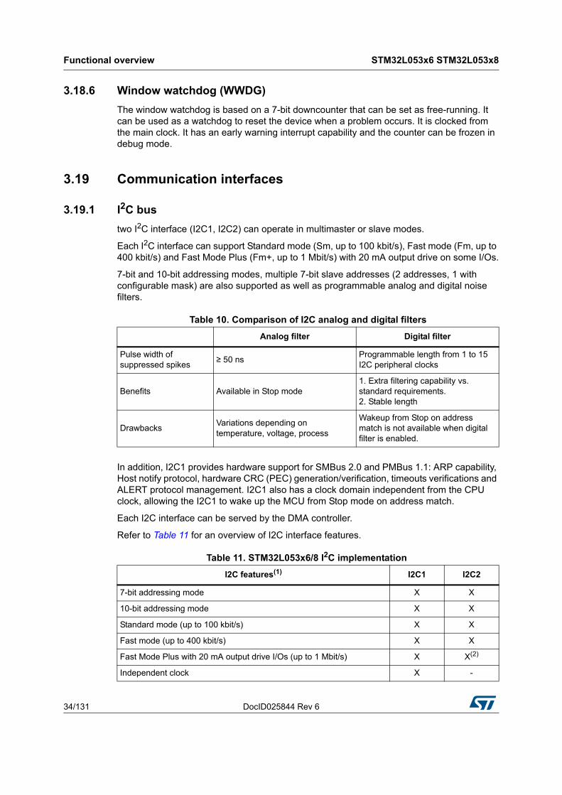
two I2C interface (I2C1, I2C2) can operate in multimaster or slave modes.
Each I2C interface can support Standard mode (Sm, up to 100 kbit/s), Fast mode (Fm, up to 400 kbit/s) and Fast Mode Plus (Fm+, up to 1 Mbit/s) with 20 mA output drive on some I/Os.
7-bit and 10-bit addressing modes, multiple 7-bit slave addresses (2 addresses, 1 with configurable mask) are also supported as well as programmable analog and digital noise filters.
In addition, I2C1 provides hardware support for SMBus 2.0 and PMBus 1.1: ARP capability, Host notify protocol, hardware CRC (PEC) generation/verification, timeouts verifications and ALERT protocol management. I2C1 also has a clock domain independent from the CPU clock, allowing the I2C1 to wake up the MCU from Stop mode on address match.
Each I2C interface can be served by the DMA controller.
Refer to Table 11 for an overview of I2C interface features.
Table 10. Comparison of I2C analog and digital filters
Analog filter Digital filter
Pulse width of suppressed spikes
≥ 50 nsProgrammable length from 1 to 15 I2C peripheral clocks
Benefits Available in Stop mode1. Extra filtering capability vs. standard requirements.2. Stable length
DrawbacksVariations depending on temperature, voltage, process
Wakeup from Stop on address match is not available when digital filter is enabled.
Table 11. STM32L053x6/8 I2C implementation
I2C features(1) I2C1 I2C2
7-bit addressing mode X X
10-bit addressing mode X X
Standard mode (up to 100 kbit/s) X X
Fast mode (up to 400 kbit/s) X X
Fast Mode Plus with 20 mA output drive I/Os (up to 1 Mbit/s) X X(2)
Independent clock X -

DocID025844 Rev 6 35/131
STM32L053x6 STM32L053x8 Functional overview
37
3.19.2 Universal synchronous/asynchronous receiver transmitter (USART)
The two USART interfaces (USART1, USART2) are able to communicate at speeds of up to 4 Mbit/s.
They provide hardware management of the CTS, RTS and RS485 driver enable (DE) signals, multiprocessor communication mode, master synchronous communication and single-wire half-duplex communication mode. They also support SmartCard communication (ISO 7816), IrDA SIR ENDEC, LIN Master/Slave capability, auto baud rate feature and has a clock domain independent from the CPU clock, allowing to wake up the MCU from Stop mode using baudrates up to 42 Kbaud.
All USART interfaces can be served by the DMA controller.
Table 12 for the supported modes and features of USART interfaces.
3.19.3 Low-power universal asynchronous receiver transmitter (LPUART)
The devices embed one Low-power UART. The LPUART supports asynchronous serial communication with minimum power consumption. It supports half duplex single wire
SMBus X -
Wakeup from STOP X -
1. X = supported.
2. See Table 15: STM32L053x6/8 pin definitions on page 41 for the list of I/Os that feature Fast Mode Plus capability
Table 11. STM32L053x6/8 I2C implementation (continued)
I2C features(1) I2C1 I2C2
Table 12. USART implementation
USART modes/features(1)
1. X = supported.
USART1 and USART2
Hardware flow control for modem X
Continuous communication using DMA X
Multiprocessor communication X
Synchronous mode(2)
2. This mode allows using the USART as an SPI master.
X
Smartcard mode X
Single-wire half-duplex communication X
IrDA SIR ENDEC block X
LIN mode X
Dual clock domain and wakeup from Stop mode X
Receiver timeout interrupt X
Modbus communication X
Auto baud rate detection (4 modes) X
Driver Enable X

Functional overview STM32L053x6 STM32L053x8
36/131 DocID025844 Rev 6
communication and modem operations (CTS/RTS). It allows multiprocessor communication.
The LPUART has a clock domain independent from the CPU clock. It can wake up the system from Stop mode using baudrates up to 46 Kbaud. The Wakeup events from Stop mode are programmable and can be:
Start bit detection
Or any received data frame
Or a specific programmed data frame
Only a 32.768 kHz clock (LSE) is needed to allow LPUART communication up to 9600 baud. Therefore, even in Stop mode, the LPUART can wait for an incoming frame while having an extremely low energy consumption. Higher speed clock can be used to reach higher baudrates.
LPUART interface can be served by the DMA controller.
3.19.4 Serial peripheral interface (SPI)/Inter-integrated sound (I2S)
Up to two SPIs are able to communicate at up to 16 Mbits/s in slave and master modes in full-duplex and half-duplex communication modes. The 3-bit prescaler gives 8 master mode frequencies and the frame is configurable to 8 bits or 16 bits. The hardware CRC generation/verification supports basic SD Card/MMC modes.
The USARTs with synchronous capability can also be used as SPI master.
One standard I2S interfaces (multiplexed with SPI2) is available. It can operate in master or slave mode, and can be configured to operate with a 16-/32-bit resolution as input or output channels. Audio sampling frequencies from 8 kHz up to 192 kHz are supported. When the I2S interfaces is configured in master mode, the master clock can be output to the external DAC/CODEC at 256 times the sampling frequency.
The SPIs can be served by the DMA controller.
Refer to Table 13 for the differences between SPI1 and SPI2.
Table 13. SPI/I2S implementation
SPI features(1)
1. X = supported.
SPI1 SPI2
Hardware CRC calculation X X
I2S mode - X
TI mode X X

DocID025844 Rev 6 37/131
STM32L053x6 STM32L053x8 Functional overview
37
3.19.5 Universal serial bus (USB)
The STM32L053x6/8 embed a full-speed USB device peripheral compliant with the USB specification version 2.0. The internal USB PHY supports USB FS signaling, embedded DP pull-up and also battery charging detection according to Battery Charging Specification Revision 1.2. The USB interface implements a full-speed (12 Mbit/s) function interface with added support for USB 2.0 Link Power Management. It has software-configurable endpoint setting with packet memory up to 1 KB and suspend/resume support. It requires a precise 48 MHz clock which can be generated from the internal main PLL (the clock source must use a HSE crystal oscillator) or by the internal 48 MHz oscillator in automatic trimming mode. The synchronization for this oscillator can be taken from the USB data stream itself (SOF signalization) which allows crystal-less operation.
3.20 Clock recovery system (CRS)
The STM32L053x6/8 embed a special block which allows automatic trimming of the internal 48 MHz oscillator to guarantee its optimal accuracy over the whole device operational range. This automatic trimming is based on the external synchronization signal, which could be either derived from USB SOF signalization, from LSE oscillator, from an external signal on CRS_SYNC pin or generated by user software. For faster lock-in during startup it is also possible to combine automatic trimming with manual trimming action.
3.21 Cyclic redundancy check (CRC) calculation unit
The CRC (cyclic redundancy check) calculation unit is used to get a CRC code using a configurable generator polynomial value and size.
Among other applications, CRC-based techniques are used to verify data transmission or storage integrity. In the scope of the EN/IEC 60335-1 standard, they offer a means of verifying the Flash memory integrity. The CRC calculation unit helps compute a signature of the software during runtime, to be compared with a reference signature generated at linktime and stored at a given memory location.
3.22 Serial wire debug port (SW-DP)
An ARM SW-DP interface is provided to allow a serial wire debugging tool to be connected to the MCU.
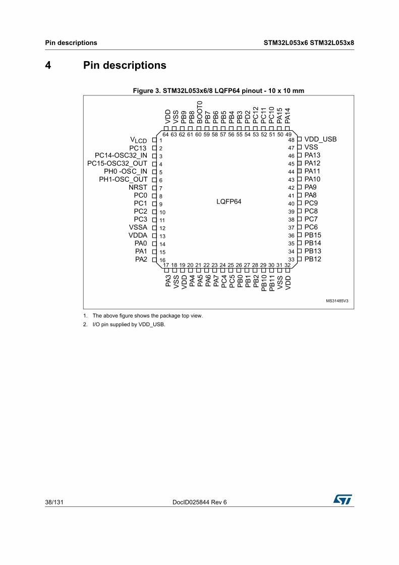
Pin descriptions STM32L053x6 STM32L053x8
38/131 DocID025844 Rev 6
4 Pin descriptions
Figure 3. STM32L053x6/8 LQFP64 pinout - 10 x 10 mm
1. The above figure shows the package top view.
2. I/O pin supplied by VDD_USB.
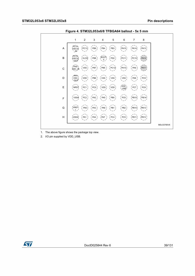
DocID025844 Rev 6 39/131
STM32L053x6 STM32L053x8 Pin descriptions
50
Figure 4. STM32L053x6/8 TFBGA64 ballout - 5x 5 mm
1. The above figure shows the package top view.
2. I/O pin supplied by VDD_USB.

Pin descriptions STM32L053x6 STM32L053x8
40/131 DocID025844 Rev 6
Figure 5. STM32L053x6/8 LQFP48 pinout - 7 x 7 mm
1. The above figure shows the package top view.
2. I/O pin supplied by VDD_USB.
Table 14. Legend/abbreviations used in the pinout table
Name Abbreviation Definition
Pin name Unless otherwise specified in brackets below the pin name, the pin function during and after reset is the same as the actual pin name
Pin type
S Supply pin
I Input only pin
I/O Input / output pin
I/O structure
FT 5 V tolerant I/O
FTf 5 V tolerant I/O, FM+ capable
TC Standard 3.3V I/O
B Dedicated BOOT0 pin
RST Bidirectional reset pin with embedded weak pull-up resistor
Notes Unless otherwise specified by a note, all I/Os are set as floating inputs during and after reset.

DocID025844 Rev 6 41/131
STM32L053x6 STM32L053x8 Pin descriptions
50
Pin functions
Alternate functions
Functions selected through GPIOx_AFR registers
Additional functions
Functions directly selected/enabled through peripheral registers
Table 14. Legend/abbreviations used in the pinout table (continued)
Name Abbreviation Definition
Table 15. STM32L053x6/8 pin definitions
Pin number
Pin name (function after
reset) Pin
typ
e
I/O s
tru
ctu
re
No
tes
Alternate functions Additional functions
LQ
FP
48
LQ
FP
64
TF
BG
A64
1 1 B2 VLCD S - - - -
2 2 A2 PC13 I/O FT - -RTC_TAMP1/RTC_TS/RT
C_OUT/WKUP2
3 3 A1PC14-OSC32_IN
(PC14)I/O FT - - OSC32_IN
4 4 B1PC15-
OSC32_OUT (PC15)
I/O TC - - OSC32_OUT
5 5 C1PH0-OSC_IN
(PH0)I/O TC - USB_CRS_SYNC OSC_IN
6 6 D1PH1-OSC_OUT
(PH1)I/O TC - - OSC_OUT
7 7 E1 NRST I/O RST - - -
- 8 E3 PC0 I/O FT -LPTIM1_IN1,
LCD_SEG18, EVENTOUT, TSC_G7_IO1
ADC_IN10
- 9 E2 PC1 I/O FT -LPTIM1_OUT,
LCD_SEG19, EVENTOUT, TSC_G7_IO2
ADC_IN11
- 10 F2 PC2 I/O FT -
LPTIM1_IN2, LCD_SEG20,
SPI2_MISO/I2S2_MCK, TSC_G7_IO3
ADC_IN12

Pin descriptions STM32L053x6 STM32L053x8
42/131 DocID025844 Rev 6
- 11 - PC3 I/O FT -
LPTIM1_ETR, LCD_SEG21,
SPI2_MOSI/I2S2_SD, TSC_G7_IO4
ADC_IN13
8 12 F1 VSSA S - - - -
- - G1 VREF+ S - - - -
9 13 H1 VDDA S - - - -
10 14 G2 PA0 I/O TC -TIM2_CH1, TSC_G1_IO1,
USART2_CTS, TIM2_ETR, COMP1_OUT
COMP1_INM6, ADC_IN0, RTC_TAMP2/WKUP1
11 15 H2 PA1 I/O FT -
EVENTOUT, LCD_SEG0, TIM2_CH2, TSC_G1_IO2,
USART2_RTS_DE, TIM21_ETR
COMP1_INP, ADC_IN1
12 16 F3 PA2 I/O FT -
TIM21_CH1, LCD_SEG1, TIM2_CH3, TSC_G1_IO3,
USART2_TX, COMP2_OUT
COMP2_INM6, ADC_IN2
13 17 G3 PA3 I/O FT -TIM21_CH2, LCD_SEG2, TIM2_CH4, TSC_G1_IO4,
USART2_RXCOMP2_INP, ADC_IN3
- 18 C2 VSS S - - -
- 19 D2 VDD S - - -
14 20 H3 PA4 I/O TC (1) SPI1_NSS, TSC_G2_IO1, USART2_CK, TIM22_ETR
COMP1_INM4, COMP2_INM4, ADC_IN4,
DAC_OUT
15 21 F4 PA5 I/O TC -SPI1_SCK, TIM2_ETR,
TSC_G2_IO2, TIM2_CH1COMP1_INM5,
COMP2_INM5, ADC_IN5
16 22 G4 PA6 I/O FT -
SPI1_MISO, LCD_SEG3, TSC_G2_IO3,
LPUART1_CTS, TIM22_CH1, EVENTOUT,
COMP1_OUT
ADC_IN6
Table 15. STM32L053x6/8 pin definitions (continued)
Pin number
Pin name (function after
reset) Pin
typ
e
I/O s
tru
ctu
re
No
tes
Alternate functions Additional functions
LQ
FP
48
LQ
FP
64
TF
BG
A64

DocID025844 Rev 6 43/131
STM32L053x6 STM32L053x8 Pin descriptions
50
17 23 H4 PA7 I/O FT -
SPI1_MOSI, LCD_SEG4, TSC_G2_IO4,
TIM22_CH2, EVENTOUT, COMP2_OUT
ADC_IN7
- 24 H5 PC4 I/O FT -EVENTOUT, LCD_SEG22,
LPUART1_TXADC_IN14
- 25 H6 PC5 I/O FT -LCD_SEG23,
LPUART1_RX, TSC_G3_IO1
ADC_IN15
18 26 F5 PB0 I/O FT -EVENTOUT, LCD_SEG5,
TSC_G3_IO2LCD_VLCD3, ADC_IN8,
VREF_OUT
19 27 G5 PB1 I/O FT -LCD_SEG6,
TSC_G3_IO3, LPUART1_RTS_DE
ADC_IN9, VREF_OUT
20 28 G6 PB2 I/O FT -LPTIM1_OUT, TSC_G3_IO4
LCD_VLCD1
21 29 G7 PB10 I/O FT -
LCD_SEG10, TIM2_CH3, TSC_SYNC,
LPUART1_TX, SPI2_SCK, I2C2_SCL
-
22 30 H7 PB11 I/O FT -EVENTOUT, LCD_SEG11, TIM2_CH4, TSC_G6_IO1, LPUART1_RX, I2C2_SDA
-
23 31 D6 VSS S - - -
24 32 E6 VDD_USB S - - -
25 33 H8 PB12 I/O FT -
SPI2_NSS/I2S2_WS, LCD_SEG12,
LPUART1_RTS_DE, TSC_G6_IO2,
I2C2_SMBA, EVENTOUT
LCD_VLCD2
26 34 G8 PB13 I/O FTf -
SPI2_SCK/I2S2_CK, LCD_SEG13, TSC_G6_IO3,
LPUART1_CTS, I2C2_SCL, TIM21_CH1
-
Table 15. STM32L053x6/8 pin definitions (continued)
Pin number
Pin name (function after
reset) Pin
typ
e
I/O s
tru
ctu
re
No
tes
Alternate functions Additional functions
LQ
FP
48
LQ
FP
64
TF
BG
A64
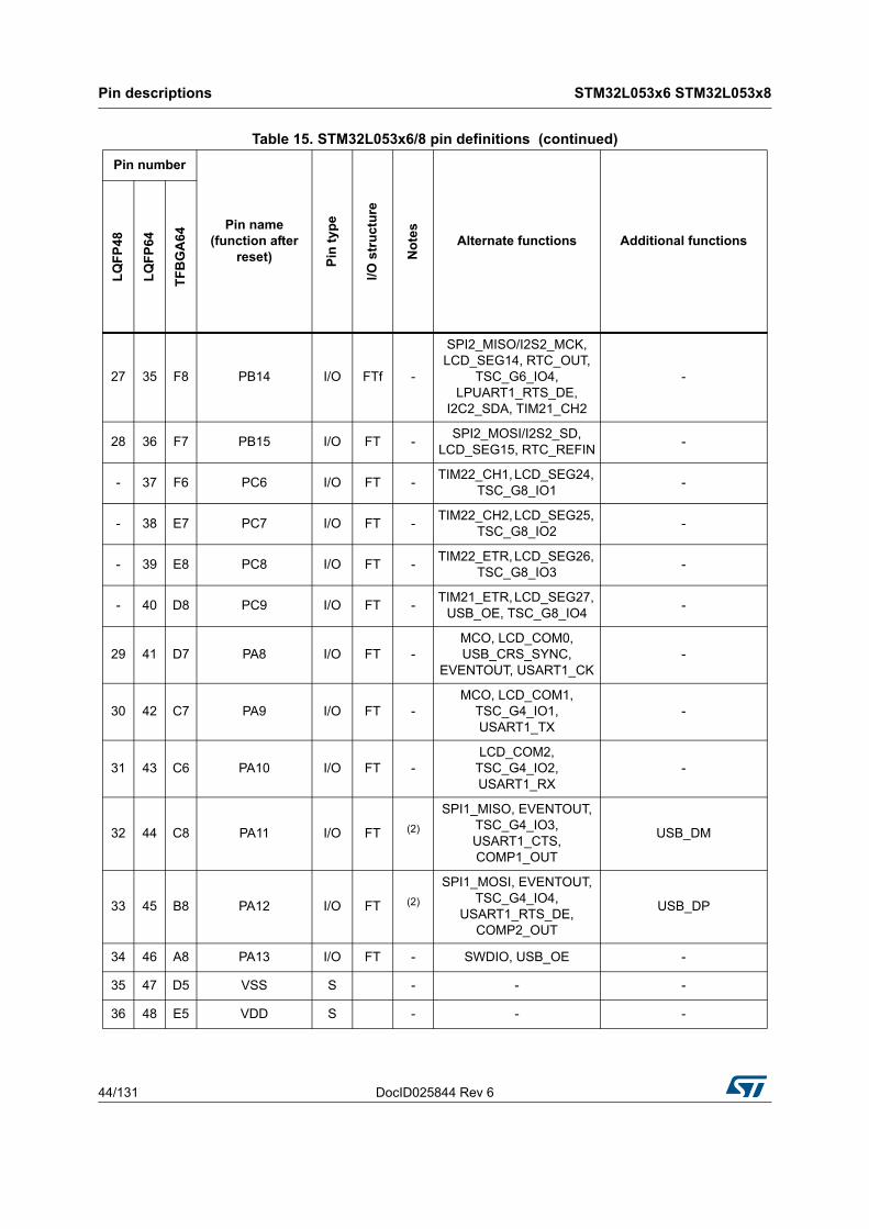
Pin descriptions STM32L053x6 STM32L053x8
44/131 DocID025844 Rev 6
27 35 F8 PB14 I/O FTf -
SPI2_MISO/I2S2_MCK, LCD_SEG14, RTC_OUT,
TSC_G6_IO4, LPUART1_RTS_DE,
I2C2_SDA, TIM21_CH2
-
28 36 F7 PB15 I/O FT -SPI2_MOSI/I2S2_SD,
LCD_SEG15, RTC_REFIN-
- 37 F6 PC6 I/O FT -TIM22_CH1, LCD_SEG24,
TSC_G8_IO1-
- 38 E7 PC7 I/O FT -TIM22_CH2, LCD_SEG25,
TSC_G8_IO2-
- 39 E8 PC8 I/O FT -TIM22_ETR, LCD_SEG26,
TSC_G8_IO3-
- 40 D8 PC9 I/O FT -TIM21_ETR, LCD_SEG27,
USB_OE, TSC_G8_IO4-
29 41 D7 PA8 I/O FT -MCO, LCD_COM0, USB_CRS_SYNC,
EVENTOUT, USART1_CK-
30 42 C7 PA9 I/O FT -MCO, LCD_COM1,
TSC_G4_IO1, USART1_TX
-
31 43 C6 PA10 I/O FT -LCD_COM2,
TSC_G4_IO2, USART1_RX
-
32 44 C8 PA11 I/O FT (2)
SPI1_MISO, EVENTOUT, TSC_G4_IO3, USART1_CTS, COMP1_OUT
USB_DM
33 45 B8 PA12 I/O FT (2)
SPI1_MOSI, EVENTOUT, TSC_G4_IO4,
USART1_RTS_DE, COMP2_OUT
USB_DP
34 46 A8 PA13 I/O FT - SWDIO, USB_OE -
35 47 D5 VSS S - - -
36 48 E5 VDD S - - -
Table 15. STM32L053x6/8 pin definitions (continued)
Pin number
Pin name (function after
reset) Pin
typ
e
I/O s
tru
ctu
re
No
tes
Alternate functions Additional functions
LQ
FP
48
LQ
FP
64
TF
BG
A64

DocID025844 Rev 6 45/131
STM32L053x6 STM32L053x8 Pin descriptions
50
37 49 A7 PA14 I/O FT - SWCLK, USART2_TX -
38 50 A6 PA15 I/O FT -SPI1_NSS, LCD_SEG17, TIM2_ETR, EVENTOUT, USART2_RX, TIM2_CH1
-
- 51 B7 PC10 I/O FT -LPUART1_TX,
LCD_COM4/LCD_SEG28/LCD_SEG40
-
- 52 B6 PC11 I/O FT -LPUART1_RX,
LCD_COM5/LCD_SEG29/LCD_SEG41
-
- 53 C5 PC12 I/O FT -LCD_COM6/LCD_SEG30/
LCD_SEG42-
- 54 B5 PD2 I/O FT -LPUART1_RTS_DE,
LCD_COM7/LCD_SEG31/LCD_SEG43
-
39 55 A5 PB3 I/O FT -SPI1_SCK, LCD_SEG7,
TIM2_CH2, TSC_G5I_O1, EVENTOUT
COMP2_INN
40 56 A4 PB4 I/O FT -SPI1_MISO, LCD_SEG8,
EVENTOUT, TSC_G5_IO2, TIM22_CH1
COMP2_INP
41 57 C4 PB5 I/O FT -SPI1_MOSI, LCD_SEG9,
LPTIM1_IN1, I2C1_SMBA, TIM22_CH2
COMP2_INP
42 58 D3 PB6 I/O FTf -USART1_TX, I2C1_SCL,
LPTIM1_ETR, TSC_G5_IO3
COMP2_INP
43 59 C3 PB7 I/O FTf -USART1_RX, I2C1_SDA,
LPTIM1_IN2, TSC_G5_IO4
COMP2_INP, PVD_IN
44 60 B4 BOOT0 I B - - -
45 61 B3 PB8 I/O FTf -LCD_SEG16, TSC_SYNC,
I2C1_SCL-
46 62 A3 PB9 I/O FTf -LCD_COM3, EVENTOUT,
I2C1_SDA, SPI2_NSS/I2S2_WS
-
Table 15. STM32L053x6/8 pin definitions (continued)
Pin number
Pin name (function after
reset) Pin
typ
e
I/O s
tru
ctu
re
No
tes
Alternate functions Additional functions
LQ
FP
48
LQ
FP
64
TF
BG
A64

Pin descriptions STM32L053x6 STM32L053x8
46/131 DocID025844 Rev 6
47 63 D4 VSS S - - - -
48 64 E4 VDD S - - - -
1. PA4 offers a reduced touch sensing sensitivity. It is thus recommended to use it as sampling capacitor I/O.
2. These pins are powered by VDD_USB. For all characteristics that refer to VDD, VDD_USB must be used instead.
Table 15. STM32L053x6/8 pin definitions (continued)
Pin number
Pin name (function after
reset) Pin
typ
e
I/O s
tru
ctu
re
No
tes
Alternate functions Additional functions
LQ
FP
48
LQ
FP
64
TF
BG
A64

ST
M3
2L0
53x6
ST
M3
2L0
53x8
Pin
de
scrip
tion
s
DocID
025844 R
ev 6
47/131
Table 16. Alternate function port A
Port
AF0 AF1 AF2 AF3 AF4 AF5 AF6 AF7
SPI1/TIM21/SYS_AF/EVENTOUT/
LCDUSB/TIM2/
EVENTOUT/TSC/
EVENTOUTUSART1/2/3 TIM2/21/22 EVENTOUT COMP1/2
Port A
PA0 - - TIM2_CH1 TSC_G1_IO1 USART2_CTS TIM2_ETR - COMP1_OUT
PA1 EVENTOUT LCD_SEG0 TIM2_CH2 TSC_G1_IO2USART2_RTS_
DETIM21_ETR - -
PA2 TIM21_CH1 LCD_SEG1 TIM2_CH3 TSC_G1_IO3 USART2_TX - - COMP2_OUT
PA3 TIM21_CH2 LCD_SEG2 TIM2_CH4 TSC_G1_IO4 USART2_RX - - -
PA4 SPI1_NSS - - TSC_G2_IO1 USART2_CK TIM22_ETR - -
PA5 SPI1_SCK - TIM2_ETR TSC_G2_IO2 - TIM2_CH1 - -
PA6 SPI1_MISO LCD_SEG3 - TSC_G2_IO3 LPUART1_CTS TIM22_CH1 EVENTOUT COMP1_OUT
PA7 SPI1_MOSI LCD_SEG4 - TSC_G2_IO4 - TIM22_CH2 EVENTOUT COMP2_OUT
PA8 MCO LCD_COM0 USB_CRS_SYNC EVENTOUT USART1_CK - - -
PA9 MCO LCD_COM1 - TSC_G4_IO1 USART1_TX - - -
PA10 - LCD_COM2 - TSC_G4_IO2 USART1_RX - - -
PA11 SPI1_MISO - EVENTOUT TSC_G4_IO3 USART1_CTS - - COMP1_OUT
PA12 SPI1_MOSI - EVENTOUT TSC_G4_IO4USART1_RTS_
DE- - COMP2_OUT
PA13 SWDIO - USB_OE - - - - -
PA14 SWCLK - - - USART2_TX - - -
PA15 SPI1_NSS LCD_SEG17 TIM2_ETR EVENTOUT USART2_RX TIM2_CH1 - -

Pin
des
criptio
ns
ST
M32
L05
3x6
ST
M32
L05
3x8
48/1
31D
ocID025
844 Re
v 6
Table 17. Alternate function port B
Port
AF0 AF1 AF2 AF3 AF4 AF5 AF6
SPI1/SPI2/I2S2/USART1/
EVENTOUT/I2C1/LCD
LPUART1/LPTIM/TIM2/SYS_AF/
EVENTOUTI2C1/TSC
I2C1/TIM22/EVENTOUT/LPUART1
SPI2/I2S2/I2C2I2C2/TIM21/EVENTOUT
Port B
PB0 EVENTOUT LCD_SEG5 - TSC_G3_IO2 - - -
PB1 - LCD_SEG6 - TSC_G3_IO3LPUART1_RTS_
DE- -
PB2 - - LPTIM1_OUT TSC_G3_IO4 - - -
PB3 SPI1_SCK LCD_SEG7 TIM2_CH2 TSC_G5I_O1 EVENTOUT - -
PB4 SPI1_MISO LCD_SEG8 EVENTOUT TSC_G5_IO2 TIM22_CH1 - -
PB5 SPI1_MOSI LCD_SEG9 LPTIM1_IN1 I2C1_SMBA TIM22_CH2 - -
PB6 USART1_TX I2C1_SCL LPTIM1_ETR TSC_G5_IO3 - - -
PB7 USART1_RX I2C1_SDA LPTIM1_IN2 TSC_G5_IO4 - - -
PB8 - LCD_SEG16 - TSC_SYNC I2C1_SCL - -
PB9 - LCD_COM3 EVENTOUT - I2C1_SDASPI2_NSS/I2S2_
WS-
PB10 - LCD_SEG10 TIM2_CH3 TSC_SYNC LPUART1_TX SPI2_SCK I2C2_SCL
PB11 EVENTOUT LCD_SEG11 TIM2_CH4 TSC_G6_IO1 LPUART1_RX - I2C2_SDA
PB12 SPI2_NSS/I2S2_WS LCD_SEG12LPUART1_RTS_
DETSC_G6_IO2 - I2C2_SMBA EVENTOUT
PB13 SPI2_SCK/I2S2_CK LCD_SEG13 - TSC_G6_IO3 LPUART1_CTS I2C2_SCL TIM21_CH1
PB14 SPI2_MISO/I2S2_MCK LCD_SEG14 RTC_OUT TSC_G6_IO4LPUART1_RTS_
DEI2C2_SDA TIM21_CH2
PB15 SPI2_MOSI/I2S2_SD LCD_SEG15 RTC_REFIN - - - -

ST
M3
2L0
53x6
ST
M3
2L0
53x8
Pin
de
scrip
tion
s
DocID
025844 R
ev 6
49/131
Table 18. Alternate function port C
Port
AF0 AF1 AF2 AF3
LPUART1/LPTIM/TIM21/12/
EVENTOUT/LCD
SPI2/I2S2/USB/LPUART1/EVENTOUT
TSC
Port C
PC0 LPTIM1_IN1 LCD_SEG18 EVENTOUT TSC_G7_IO1
PC1 LPTIM1_OUT LCD_SEG19 EVENTOUT TSC_G7_IO2
PC2 LPTIM1_IN2 LCD_SEG20 SPI2_MISO/I2S2_MCK TSC_G7_IO3
PC3 LPTIM1_ETR LCD_SEG21 SPI2_MOSI/I2S2_SD TSC_G7_IO4
PC4 EVENTOUT LCD_SEG22 LPUART1_TX -
PC5 - LCD_SEG23 LPUART1_RX TSC_G3_IO1
PC6 TIM22_CH1 LCD_SEG24 - TSC_G8_IO1
PC7 TIM22_CH2 LCD_SEG25 - TSC_G8_IO2
PC8 TIM22_ETR LCD_SEG26 - TSC_G8_IO3
PC9 TIM21_ETR LCD_SEG27 USB_OE TSC_G8_IO4
PC10 LPUART1_TX LCD_COM4/LCD_SEG28 - -
PC11 LPUART1_RX LCD_COM5/LCD_SEG29 - -
PC12 - LCD_COM6/LCD_SEG30 - -
PC13 - - - -
PC14 - - - -
PC15 - - - -
Table 19. Alternate function port D
PortAF0 AF1
LPUART1 LCD
Port D PD2 LPUART1_RTS_DE LCD_COM7/LCD_SEG31
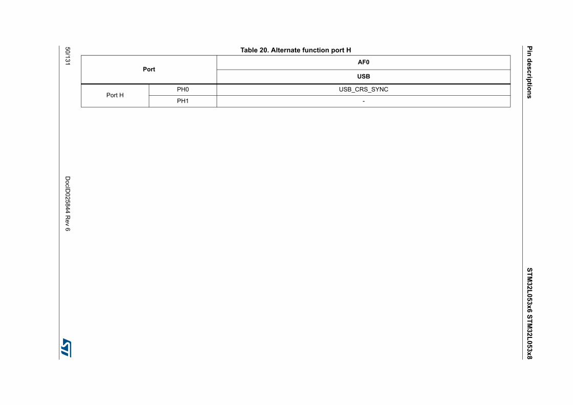
Pin
des
criptio
ns
ST
M32
L05
3x6
ST
M32
L05
3x8
50/1
31D
ocID025
844 Re
v 6
Table 20. Alternate function port H
PortAF0
USB
Port HPH0 USB_CRS_SYNC
PH1 -

DocID025844 Rev 6 51/131
STM32L053x6 STM32L053x8 Memory mapping
51
5 Memory mapping
Figure 6. Memory map
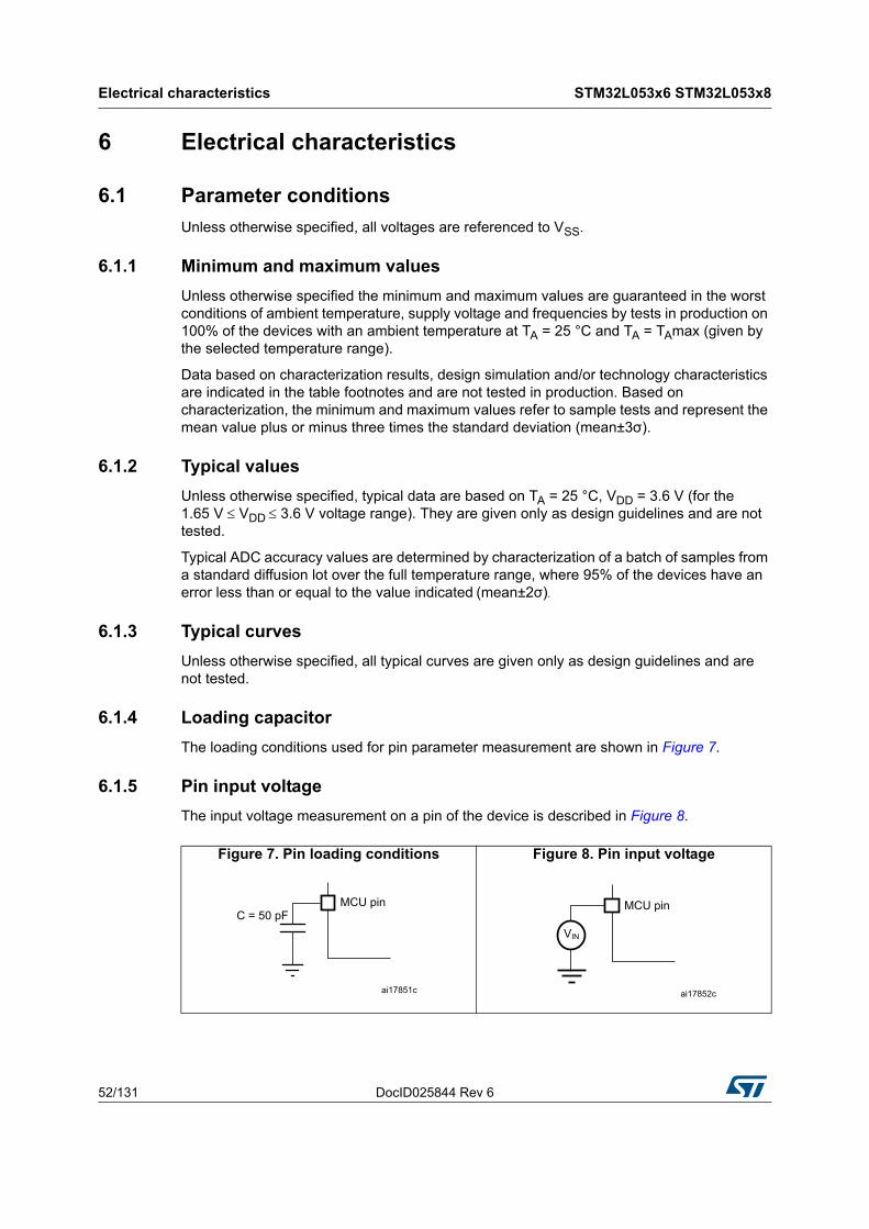
Electrical characteristics STM32L053x6 STM32L053x8
52/131 DocID025844 Rev 6
6 Electrical characteristics
6.1 Parameter conditions
Unless otherwise specified, all voltages are referenced to VSS.
6.1.1 Minimum and maximum values
Unless otherwise specified the minimum and maximum values are guaranteed in the worst conditions of ambient temperature, supply voltage and frequencies by tests in production on 100% of the devices with an ambient temperature at TA = 25 °C and TA = TAmax (given by the selected temperature range).
Data based on characterization results, design simulation and/or technology characteristics are indicated in the table footnotes and are not tested in production. Based on characterization, the minimum and maximum values refer to sample tests and represent the mean value plus or minus three times the standard deviation (mean±3σ).
6.1.2 Typical values
Unless otherwise specified, typical data are based on TA = 25 °C, VDD = 3.6 V (for the 1.65 V VDD 3.6 V voltage range). They are given only as design guidelines and are not tested.
Typical ADC accuracy values are determined by characterization of a batch of samples from a standard diffusion lot over the full temperature range, where 95% of the devices have an error less than or equal to the value indicated (mean±2σ).
6.1.3 Typical curves
Unless otherwise specified, all typical curves are given only as design guidelines and are not tested.
6.1.4 Loading capacitor
The loading conditions used for pin parameter measurement are shown in Figure 7.
6.1.5 Pin input voltage
The input voltage measurement on a pin of the device is described in Figure 8.
Figure 7. Pin loading conditions Figure 8. Pin input voltage

DocID025844 Rev 6 53/131
STM32L053x6 STM32L053x8 Electrical characteristics
112
6.1.6 Power supply scheme
Figure 9. Power supply scheme

Electrical characteristics STM32L053x6 STM32L053x8
54/131 DocID025844 Rev 6
6.1.7 Optional LCD power supply scheme
Figure 10. Optional LCD power supply scheme
1. Option 1: LCD power supply is provided by a dedicated VLCD supply source, VSEL switch is open.
2. Option 2: LCD power supply is provided by the internal step-up converter, VSEL switch is closed, an external capacitance is needed for correct behavior of this converter.
6.1.8 Current consumption measurement
Figure 11. Current consumption measurement scheme
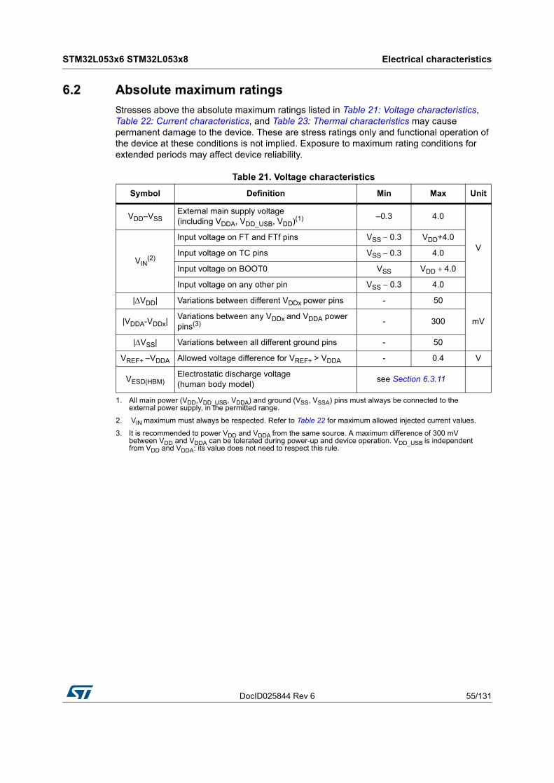
DocID025844 Rev 6 55/131
STM32L053x6 STM32L053x8 Electrical characteristics
112
6.2 Absolute maximum ratings
Stresses above the absolute maximum ratings listed in Table 21: Voltage characteristics, Table 22: Current characteristics, and Table 23: Thermal characteristics may cause permanent damage to the device. These are stress ratings only and functional operation of the device at these conditions is not implied. Exposure to maximum rating conditions for extended periods may affect device reliability.
Table 21. Voltage characteristics
Symbol Definition Min Max Unit
VDD–VSSExternal main supply voltage (including VDDA, VDD_USB, VDD)(1)
1. All main power (VDD,VDD_USB, VDDA) and ground (VSS, VSSA) pins must always be connected to the external power supply, in the permitted range.
–0.3 4.0
V
VIN(2)
2. VIN maximum must always be respected. Refer to Table 22 for maximum allowed injected current values.
Input voltage on FT and FTf pins VSS 0.3 VDD+4.0
Input voltage on TC pins VSS 0.3 4.0
Input voltage on BOOT0 VSS VDD 4.0
Input voltage on any other pin VSS 0.3 4.0
|VDD| Variations between different VDDx power pins - 50
mV|VDDA-VDDx|Variations between any VDDx and VDDA power pins(3)
3. It is recommended to power VDD and VDDA from the same source. A maximum difference of 300 mV between VDD and VDDA can be tolerated during power-up and device operation. VDD_USB is independent from VDD and VDDA: its value does not need to respect this rule.
- 300
|VSS| Variations between all different ground pins - 50
VREF+ –VDDA Allowed voltage difference for VREF+ > VDDA - 0.4 V
VESD(HBM)Electrostatic discharge voltage (human body model)
see Section 6.3.11

Electrical characteristics STM32L053x6 STM32L053x8
56/131 DocID025844 Rev 6
Table 22. Current characteristics
Symbol Ratings Max. Unit
ΣIVDD(2) Total current into sum of all VDD power lines (source)(1)
1. All main power (VDD, VDDA) and ground (VSS, VSSA) pins must always be connected to the external power supply, in the permitted range.
105
mA
ΣIVSS(2)
2. This current consumption must be correctly distributed over all I/Os and control pins. The total output current must not be sunk/sourced between two consecutive power supply pins referring to high pin count LQFP packages.
Total current out of sum of all VSS ground lines (sink)(1) 105
ΣIVDD_USB Total current into VDD_USB power lines (source) 25
IVDD(PIN) Maximum current into each VDD power pin (source)(1) 100
IVSS(PIN) Maximum current out of each VSS ground pin (sink)(1) 100
IIO
Output current sunk by any I/O and control pin except FTf pins
16
Output current sunk by FTf pins 22
Output current sourced by any I/O and control pin -16
ΣIIO(PIN)
Total output current sunk by sum of all IOs and control pins except PA11 and PA12(2) 90
Total output current sunk by PA11 and PA12 25
Total output current sourced by sum of all IOs and control pins(2) -90
IINJ(PIN)
Injected current on FT, FFf, RST and B pins -5/+0(3)
3. Positive current injection is not possible on these I/Os. A negative injection is induced by VIN<VSS. IINJ(PIN) must never be exceeded. Refer to Table 21 for maximum allowed input voltage values.
Injected current on TC pin ± 5(4)
4. A positive injection is induced by VIN > VDD while a negative injection is induced by VIN < VSS. IINJ(PIN) must never be exceeded. Refer to Table 21: Voltage characteristics for the maximum allowed input voltage values.
ΣIINJ(PIN) Total injected current (sum of all I/O and control pins)(5)
5. When several inputs are submitted to a current injection, the maximum IINJ(PIN) is the absolute sum of the positive and negative injected currents (instantaneous values).
± 25
Table 23. Thermal characteristics
Symbol Ratings Value Unit
TSTG Storage temperature range –65 to +150 °C
TJ Maximum junction temperature 150 °C
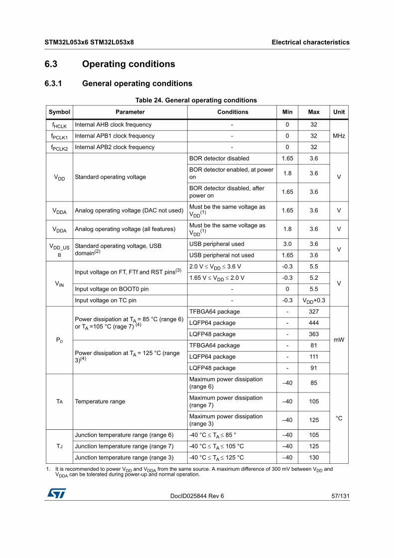
DocID025844 Rev 6 57/131
STM32L053x6 STM32L053x8 Electrical characteristics
112
6.3 Operating conditions
6.3.1 General operating conditions
Table 24. General operating conditions
Symbol Parameter Conditions Min Max Unit
fHCLK Internal AHB clock frequency - 0 32
MHzfPCLK1 Internal APB1 clock frequency - 0 32
fPCLK2 Internal APB2 clock frequency - 0 32
VDD Standard operating voltage
BOR detector disabled 1.65 3.6
VBOR detector enabled, at power on
1.8 3.6
BOR detector disabled, after power on
1.65 3.6
VDDA Analog operating voltage (DAC not used)Must be the same voltage as VDD
(1) 1.65 3.6 V
VDDA Analog operating voltage (all features)Must be the same voltage as VDD
(1) 1.8 3.6 V
VDD_US
B
Standard operating voltage, USB domain(2)
USB peripheral used 3.0 3.6V
USB peripheral not used 1.65 3.6
VIN
Input voltage on FT, FTf and RST pins(3)2.0 V VDD 3.6 V -0.3 5.5
V1.65 V VDD 2.0 V -0.3 5.2
Input voltage on BOOT0 pin - 0 5.5
Input voltage on TC pin - -0.3 VDD+0.3
PD
Power dissipation at TA = 85 °C (range 6) or TA =105 °C (rage 7) (4)
TFBGA64 package - 327
mW
LQFP64 package - 444
LQFP48 package - 363
Power dissipation at TA = 125 °C (range 3)(4)
TFBGA64 package - 81
LQFP64 package - 111
LQFP48 package - 91
TA Temperature range
Maximum power dissipation (range 6)
–40 85
°C
Maximum power dissipation (range 7)
–40 105
Maximum power dissipation (range 3)
–40 125
TJ
Junction temperature range (range 6) -40 °C TA 85 ° –40 105
Junction temperature range (range 7) -40 °C TA 105 °C –40 125
Junction temperature range (range 3) -40 °C TA 125 °C –40 130
1. It is recommended to power VDD and VDDA from the same source. A maximum difference of 300 mV between VDD and VDDA can be tolerated during power-up and normal operation.

Electrical characteristics STM32L053x6 STM32L053x8
58/131 DocID025844 Rev 6
2. VDD_USB must respect the following conditions:
- When VDD is powered on (VDD < VDD_min), VDD_USB should be always lower than VDD.
- When VDD is powered down (VDD < VDD_min), VDD_USB should be always lower than VDD.
- In operating mode, VDD_USB could be lower or higher VDD.
- If the USB is not used, VDD_USB must range from VDD_min to VDD_max to be able to use PA11 and PA12 as standard I/Os.
3. To sustain a voltage higher than VDD+0.3V, the internal pull-up/pull-down resistors must be disabled.
4. If TA is lower, higher PD values are allowed as long as TJ does not exceed TJ max (see Table 85: Thermal characteristics on page 123).

DocID025844 Rev 6 59/131
STM32L053x6 STM32L053x8 Electrical characteristics
112
6.3.2 Embedded reset and power control block characteristics
The parameters given in the following table are derived from the tests performed under the ambient temperature condition summarized in Table 24.
Table 25. Embedded reset and power control block characteristics
Symbol Parameter Conditions Min Typ Max Unit
tVDD(1)
VDD rise time rateBOR detector enabled 0 -
µs/VBOR detector disabled 0 - 1000
VDD fall time rateBOR detector enabled 20 -
BOR detector disabled 0 - 1000
TRSTTEMPO(1) Reset temporization
VDD rising, BOR enabled - 2 3.3ms
VDD rising, BOR disabled(2) 0.4 0.7 1.6
VPOR/PDRPower on/power down reset threshold
Falling edge 1 1.5 1.65
V
Rising edge 1.3 1.5 1.65
VBOR0 Brown-out reset threshold 0Falling edge 1.67 1.7 1.74
Rising edge 1.69 1.76 1.8
VBOR1 Brown-out reset threshold 1Falling edge 1.87 1.93 1.97
Rising edge 1.96 2.03 2.07
VBOR2 Brown-out reset threshold 2Falling edge 2.22 2.30 2.35
Rising edge 2.31 2.41 2.44
VBOR3 Brown-out reset threshold 3Falling edge 2.45 2.55 2.6
Rising edge 2.54 2.66 2.7
VBOR4 Brown-out reset threshold 4Falling edge 2.68 2.8 2.85
Rising edge 2.78 2.9 2.95
VPVD0Programmable voltage detector threshold 0
Falling edge 1.8 1.85 1.88
Rising edge 1.88 1.94 1.99
VPVD1 PVD threshold 1Falling edge 1.98 2.04 2.09
Rising edge 2.08 2.14 2.18
VPVD2 PVD threshold 2Falling edge 2.20 2.24 2.28
Rising edge 2.28 2.34 2.38
VPVD3 PVD threshold 3Falling edge 2.39 2.44 2.48
Rising edge 2.47 2.54 2.58
VPVD4 PVD threshold 4Falling edge 2.57 2.64 2.69
Rising edge 2.68 2.74 2.79
VPVD5 PVD threshold 5Falling edge 2.77 2.83 2.88
Rising edge 2.87 2.94 2.99

Electrical characteristics STM32L053x6 STM32L053x8
60/131 DocID025844 Rev 6
6.3.3 Embedded internal reference voltage
The parameters given in Table 27 are based on characterization results, unless otherwise specified.
VPVD6 PVD threshold 6Falling edge 2.97 3.05 3.09
VRising edge 3.08 3.15 3.20
Vhyst Hysteresis voltage
BOR0 threshold - 40 -
mVAll BOR and PVD thresholds excepting BOR0
- 100 -
1. Guaranteed by characterization results.
2. Valid for device version without BOR at power up. Please see option "D" in Ordering information scheme for more details.
Table 25. Embedded reset and power control block characteristics (continued)
Symbol Parameter Conditions Min Typ Max Unit
Table 26. Embedded internal reference voltage calibration values
Calibration value name Description Memory address
VREFINT_CALRaw data acquired at temperature of 25 °CVDDA= 3 V
0x1FF8 0078 - 0x1FF8 0079
Table 27. Embedded internal reference voltage(1)
Symbol Parameter Conditions Min Typ Max Unit
VREFINT out(2) Internal reference voltage – 40 °C < TJ < +125 °C 1.202 1.224 1.242 V
TVREFINT Internal reference startup time - - 2 3 ms
VVREF_MEASVDDA and VREF+ voltage during VREFINT factory measure
- 2.99 3 3.01 V
AVREF_MEASAccuracy of factory-measured VREFINT value(3)
Including uncertainties due to ADC and VDDA/VREF+ values
- - ±5 mV
TCoeff(4) Temperature coefficient –40 °C < TJ < +125 °C - 25 100 ppm/°C
ACoeff(4) Long-term stability 1000 hours, T= 25 °C - - 1000 ppm
VDDCoeff(4) Voltage coefficient 3.0 V < VDDA < 3.6 V - - 2000 ppm/V
TS_vrefint(4)(5)
ADC sampling time when reading the internal reference voltage
- 5 10 - µs
TADC_BUF(4) Startup time of reference
voltage buffer for ADC- - - 10 µs
IBUF_ADC(4) Consumption of reference
voltage buffer for ADC- - 13.5 25 µA
IVREF_OUT(4) VREF_OUT output current(6) - - - 1 µA
CVREF_OUT(4) VREF_OUT output load - - - 50 pF
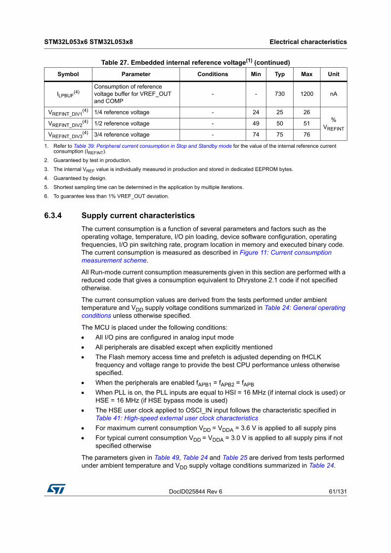
DocID025844 Rev 6 61/131
STM32L053x6 STM32L053x8 Electrical characteristics
112
6.3.4 Supply current characteristics
The current consumption is a function of several parameters and factors such as the operating voltage, temperature, I/O pin loading, device software configuration, operating frequencies, I/O pin switching rate, program location in memory and executed binary code. The current consumption is measured as described in Figure 11: Current consumption measurement scheme.
All Run-mode current consumption measurements given in this section are performed with a reduced code that gives a consumption equivalent to Dhrystone 2.1 code if not specified otherwise.
The current consumption values are derived from the tests performed under ambient temperature and VDD supply voltage conditions summarized in Table 24: General operating conditions unless otherwise specified.
The MCU is placed under the following conditions:
All I/O pins are configured in analog input mode
All peripherals are disabled except when explicitly mentioned
The Flash memory access time and prefetch is adjusted depending on fHCLK frequency and voltage range to provide the best CPU performance unless otherwise specified.
When the peripherals are enabled fAPB1 = fAPB2 = fAPB
When PLL is on, the PLL inputs are equal to HSI = 16 MHz (if internal clock is used) or HSE = 16 MHz (if HSE bypass mode is used)
The HSE user clock applied to OSCI_IN input follows the characteristic specified in Table 41: High-speed external user clock characteristics
For maximum current consumption VDD = VDDA = 3.6 V is applied to all supply pins
For typical current consumption VDD = VDDA = 3.0 V is applied to all supply pins if not specified otherwise
The parameters given in Table 49, Table 24 and Table 25 are derived from tests performed under ambient temperature and VDD supply voltage conditions summarized in Table 24.
ILPBUF(4)
Consumption of reference voltage buffer for VREF_OUT and COMP
- - 730 1200 nA
VREFINT_DIV1(4) 1/4 reference voltage - 24 25 26
% VREFINT
VREFINT_DIV2(4) 1/2 reference voltage - 49 50 51
VREFINT_DIV3(4) 3/4 reference voltage - 74 75 76
1. Refer to Table 39: Peripheral current consumption in Stop and Standby mode for the value of the internal reference current consumption (IREFINT).
2. Guaranteed by test in production.
3. The internal VREF value is individually measured in production and stored in dedicated EEPROM bytes.
4. Guaranteed by design.
5. Shortest sampling time can be determined in the application by multiple iterations.
6. To guarantee less than 1% VREF_OUT deviation.
Table 27. Embedded internal reference voltage(1) (continued)
Symbol Parameter Conditions Min Typ Max Unit

Electrical characteristics STM32L053x6 STM32L053x8
62/131 DocID025844 Rev 6
Table 28. Current consumption in Run mode, code with data processing running from Flash
Symbol Parameter Conditions fHCLK Typ Max(1) Unit
IDD(Run from Flash)
Supply current in Run mode, code executed from Flash
fHSE = fHCLK up to 16 MHz included,
fHSE = fHCLK/2 above 16 MHz (PLL on)(2)
Range 3, VCORE=1.2 V
VOS[1:0]=11
1 MHz 165 230
µA2 MHz 290 360
4 MHz 555 630
Range 2, VCORE=1.5 V, VOS[1:0]=10,
4 MHz 0.665 0.74
mA
8 MHz 1.3 1.4
16 MHz 2.6 2.8
Range 1, VCORE=1.8 V, VOS[1:0]=01
8 MHz 1.55 1.7
16 MHz 3.1 3.4
32 MHz 6.3 6.8
MSI clockRange 3, VCORE=1.2 V, VOS[1:0]=11
65 kHz 36.5 110
µA524 kHz 99.5 190
4.2 MHz 620 700
HSI clock
Range 2, VCORE=1.5 V, VOS[1:0]=10,
16 MHz 2.6 2.9
mARange 1, VCORE=1.8 V, VOS[1:0]=01
32 MHz 6.25 7
1. Guaranteed by characterization results at 125 °C, unless otherwise specified.
2. Oscillator bypassed (HSEBYP = 1 in RCC_CR register).
Table 29. Current consumption in Run mode vs code type, code with data processing running from Flash
Symbol Parameter Conditions fHCLK Typ Unit
IDD(Run from Flash)
Supply current in Run mode, code executed from Flash
fHSE = fHCLK up to 16 MHz included,
fHSE = fHCLK/2 above 16 MHz (PLL on)(1)
Range 3, VCORE=1.2 V, VOS[1:0]=11
Dhrystone
4 MHz
555
µA
CoreMark 585
Fibonacci 440
while(1) 355
while(1), prefetch off
353
Range 1, VCORE=1.8 V, VOS[1:0]=01
Dhrystone
32 MHz
6.3
mA
CoreMark 6.3
Fibonacci 6.55
while(1) 5.4
while(1), prefetch off
5.2
1. Oscillator bypassed (HSEBYP = 1 in RCC_CR register).

DocID025844 Rev 6 63/131
STM32L053x6 STM32L053x8 Electrical characteristics
112
Figure 12. IDD vs VDD, at TA= 25/55/85/105 °C, Run mode, code running from Flash memory, Range 2, HSE, 1WS
Figure 13. IDD vs VDD, at TA= 25/55/85/105 °C, Run mode, code running from Flash memory, Range 2, HSI16, 1WS

Electrical characteristics STM32L053x6 STM32L053x8
64/131 DocID025844 Rev 6
Table 30. Current consumption in Run mode, code with data processing running from RAM
Symbol Parameter Conditions fHCLK Typ Max(1) Unit
IDD (Run from RAM)
Supply current in Run mode, code executed from RAM, Flash switched off
fHSE = fHCLK up to 16 MHz included,
fHSE = fHCLK/2 above 16 MHz (PLL on)(2)
Range 3, VCORE=1.2 V, VOS[1:0]=11
1 MHz 135 170
µA2 MHz 240 270
4 MHz 450 480
Range 2, VCORE=1.5 ,V, VOS[1:0]=10
4 MHz 0.52 0.6
mA
8 MHz 1 1.2
16 MHz 2 2.3
Range 1, VCORE=1.8 V, VOS[1:0]=01
8 MHz 1.25 1.4
16 MHz 2.45 2.8
32 MHz 5.1 5.4
MSI clockRange 3, VCORE=1.2 V, VOS[1:0]=11
65 kHz 34.5 75
µA524 kHz 83 120
4.2 MHz 485 540
HSI16 clock source (16 MHz)
Range 2, VCORE=1.5 V, VOS[1:0]=10
16 MHz 2.1 2.3
mARange 1, VCORE=1.8 V, VOS[1:0]=01
32 MHz 5.1 5.6
1. Guaranteed by characterization results at 125 °C, unless otherwise specified.
2. Oscillator bypassed (HSEBYP = 1 in RCC_CR register).
Table 31. Current consumption in Run mode vs code type, code with data processing running from RAM(1)
Symbol Parameter Conditions fHCLK Typ Unit
IDD (Run from RAM)
Supply current in Run mode, code executed from RAM, Flash switched off
fHSE = fHCLK up to 16 MHz included,
fHSE = fHCLK/2 above 16 MHz (PLL on)(2)
Range 3, VCORE=1.2 V, VOS[1:0]=11
Dhrystone
4 MHz
450
µACoreMark 575
Fibonacci 370
while(1) 340
Range 1, VCORE=1.8 V, VOS[1:0]=01
Dhrystone
32 MHz
5.1
mACoreMark 6.25
Fibonacci 4.4
while(1) 4.7
1. Guaranteed by characterization results, unless otherwise specified.
2. Oscillator bypassed (HSEBYP = 1 in RCC_CR register).
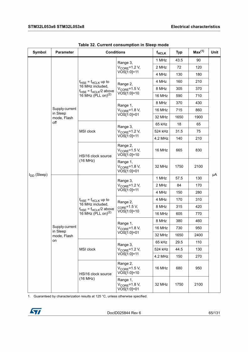
DocID025844 Rev 6 65/131
STM32L053x6 STM32L053x8 Electrical characteristics
112
Table 32. Current consumption in Sleep mode
Symbol Parameter Conditions fHCLK Typ Max(1) Unit
IDD (Sleep)
Supply current in Sleep mode, Flash off
fHSE = fHCLK up to 16 MHz included, fHSE = fHCLK/2 above 16 MHz (PLL on)(2)
Range 3, VCORE=1.2 V, VOS[1:0]=11
1 MHz 43.5 90
µA
2 MHz 72 120
4 MHz 130 180
Range 2, VCORE=1.5 V, VOS[1:0]=10
4 MHz 160 210
8 MHz 305 370
16 MHz 590 710
Range 1, VCORE=1.8 V, VOS[1:0]=01
8 MHz 370 430
16 MHz 715 860
32 MHz 1650 1900
MSI clockRange 3, VCORE=1.2 V, VOS[1:0]=11
65 kHz 18 65
524 kHz 31.5 75
4.2 MHz 140 210
HSI16 clock source (16 MHz)
Range 2, VCORE=1.5 V, VOS[1:0]=10
16 MHz 665 830
Range 1, VCORE=1.8 V, VOS[1:0]=01
32 MHz 1750 2100
Supply current in Sleep mode, Flash on
fHSE = fHCLK up to 16 MHz included, fHSE = fHCLK/2 above 16 MHz (PLL on)(2)
Range 3, VCORE=1.2 V, VOS[1:0]=11
1 MHz 57.5 130
2 MHz 84 170
4 MHz 150 280
Range 2,
CORE=1.5 V, VOS[1:0]=10
4 MHz 170 310
8 MHz 315 420
16 MHz 605 770
Range 1, VCORE=1.8 V, VOS[1:0]=01
8 MHz 380 460
16 MHz 730 950
32 MHz 1650 2400
MSI clockRange 3, VCORE=1.2 V, VOS[1:0]=11
65 kHz 29.5 110
524 kHz 44.5 130
4.2 MHz 150 270
HSI16 clock source (16 MHz)
Range 2, VCORE=1.5 V, VOS[1:0]=10
16 MHz 680 950
Range 1, VCORE=1.8 V, VOS[1:0]=01
32 MHz 1750 2100
1. Guaranteed by characterization results at 125 °C, unless otherwise specified.

Electrical characteristics STM32L053x6 STM32L053x8
66/131 DocID025844 Rev 6
2. Oscillator bypassed (HSEBYP = 1 in RCC_CR register).
Table 33. Current consumption in Low-power run mode
Symbol Parameter Conditions Typ Max(1) Unit
IDD (LP Run)
Supply current in
Low-power run mode
All peripherals off, code
executed from RAM, Flash switched off,
VDD from 1.65 to 3.6 V
MSI clock = 65 kHz,fHCLK = 32 kHz
TA = − 40 to 25°C 8.5 10
µA
TA = 85 °C 11.5 48
TA = 105 °C 15.5 53
TA = 125 °C 27.5 130
MSI clock= 65 kHz, fHCLK = 65 kHz
TA =-40 °C to 25 °C 10 15
TA = 85 °C 15.5 50
TA = 105 °C 19.5 54
TA = 125 °C 31.5 130
MSI clock= 131 kHz, fHCLK = 131 kHz
TA = − 40 to 25°C 20 25
TA = 55 °C 23 50
TA = 85 °C 25.5 55
TA = 105 °C 29.5 64
TA = 125 °C 40 140
All peripherals off, code
executed from Flash, VDD
from 1.65 V to 3.6 V
MSI clock= 65 kHz,fHCLK = 32 kHz
TA = − 40 to 25°C 22 28
TA = 85 °C 26 68
TA = 105 °C 31 75
TA = 125 °C 44 95
MSI clock = 65 kHz,fHCLK = 65 kHz
TA = − 40 to 25°C 27.5 33
TA = 85 °C 31.5 73
TA = 105 °C 36.5 80
TA = 125 °C 49 100
MSI clock = 131 kHz,
fHCLK = 131 kHz
TA = − 40 to 25°C 39 46
TA = 55 °C 41 80
TA = 85 °C 44 86
TA = 105 °C 49.5 100
TA = 125 °C 60 120
1. Guaranteed by characterization results at 125 °C, unless otherwise specified.

DocID025844 Rev 6 67/131
STM32L053x6 STM32L053x8 Electrical characteristics
112
Figure 14. IDD vs VDD, at TA= 25/55/ 85/105/125 °C, Low-power run mode, code runningfrom RAM, Range 3, MSI (Range 0) at 64 KHz, 0 WS
Table 34. Current consumption in Low-power sleep mode
Symbol Parameter Conditions Typ Max(1) Unit
IDD (LP Sleep)
Supply current in
Low-power sleep mode
All peripherals off, VDD from 1.65 to 3.6 V
MSI clock = 65 kHz, fHCLK = 32 kHz,
Flash offTA = − 40 to 25°C 4.7(2) -
µA
MSI clock = 65 kHz, fHCLK = 32 kHz,
Flash on
TA = − 40 to 25°C 17 23
TA = 85 °C 19.5 63
TA = 105 °C 23 69
TA = 125 °C 32.5 90
MSI clock =65 kHz,fHCLK = 65 kHz,
Flash on
TA = − 40 to 25°C 17 23
TA = 85 °C 20 63
TA = 105 °C 23.5 69
TA = 125 °C 32.5 90
MSI clock = 131 kHz, fHCLK = 131 kHz,
Flash on
TA = − 40 to 25°C 19.5 36
TA = 55 °C 20.5 64
TA = 85 °C 22.5 66
TA = 105 °C 26 72
TA = 125 °C 35 95
1. Guaranteed by characterization results at 125 °C, unless otherwise specified.
2. As the CPU is in Sleep mode, the difference between the current consumption with Flash on and off (nearly 12 µA) is the same whatever the clock frequency.
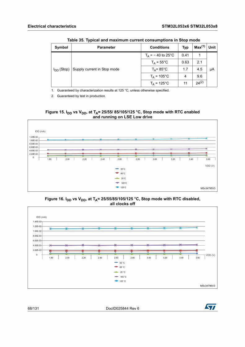
Electrical characteristics STM32L053x6 STM32L053x8
68/131 DocID025844 Rev 6
Figure 15. IDD vs VDD, at TA= 25/55/ 85/105/125 °C, Stop mode with RTC enabled and running on LSE Low drive
Figure 16. IDD vs VDD, at TA= 25/55/85/105/125 °C, Stop mode with RTC disabled, all clocks off
Table 35. Typical and maximum current consumptions in Stop mode
Symbol Parameter Conditions Typ Max(1)
1. Guaranteed by characterization results at 125 °C, unless otherwise specified.
Unit
IDD (Stop) Supply current in Stop mode
TA = − 40 to 25°C 0.41 1
µA
TA = 55°C 0.63 2.1
TA= 85°C 1.7 4.5
TA = 105°C 4 9.6
TA = 125°C 11 24(2)
2. Guaranteed by test in production.

DocID025844 Rev 6 69/131
STM32L053x6 STM32L053x8 Electrical characteristics
112
Table 36. Typical and maximum current consumptions in Standby mode
Symbol Parameter Conditions Typ Max(1) Unit
IDD (Standby)
Supply current in Standby mode
Independent watchdog and LSI enabled
TA = − 40 to 25°C 1.3 1.7
µA
TA = 55 °C - 2.9
TA= 85 °C - 3.3
TA = 105 °C - 4.1
TA = 125 °C - 8.5
Independent watchdog and LSI off
TA = − 40 to 25°C 0.29 0.6
TA = 55 °C 0.32 0.9
TA = 85 °C 0.5 2.3
TA = 105 °C 0.94 3
TA = 125 °C 2.6 7
1. Guaranteed by characterization results at 125 °C, unless otherwise specified
Table 37. Average current consumption during Wakeup
Symbol parameter System frequencyCurrent
consumption during wakeup
Unit
IDD (Wakeup from Stop)
Supply current during Wakeup from Stop mode
HSI 1
mA
HSI/4 0,7
MSI clock = 4,2 MHz 0,7
MSI clock = 1,05 MHz 0,4
MSI clock = 65 KHz 0,1
IDD (Reset) Reset pin pulled down - 0,21
IDD (Power-up) BOR on - 0,23
IDD (Wakeup from StandBy)
With Fast wakeup set MSI clock = 2,1 MHz 0,5
With Fast wakeup disabled MSI clock = 2,1 MHz 0,12

Electrical characteristics STM32L053x6 STM32L053x8
70/131 DocID025844 Rev 6
On-chip peripheral current consumption
The current consumption of the on-chip peripherals is given in the following tables. The MCU is placed under the following conditions:
all I/O pins are in input mode with a static value at VDD or VSS (no load)
all peripherals are disabled unless otherwise mentioned
the given value is calculated by measuring the current consumption
– with all peripherals clocked off
– with only one peripheral clocked on
Table 38. Peripheral current consumption in Run or Sleep mode(1)
Peripheral
Typical consumption, VDD = 3.0 V, TA = 25 °C
UnitRange 1, VCORE=1.8 V
VOS[1:0] = 01
Range 2, VCORE=1.5 V
VOS[1:0] = 10
Range 3, VCORE=1.2 V VOS[1:0] = 11
Low-power sleep and
run
APB1
CRS 2.5 2 2 2
µA/MHz (fHCLK)
DAC1 4 3.5 3 2.5
I2C1 11 9.5 7.5 9
I2C2 4 3.5 3 2.5
LCD1 4 3.5 3 2.5
LPTIM1 10 8.5 6.5 8
LPUART1 8 6.5 5.5 6
SPI2 9 4.5 3.5 4
USB 8.5 4.5 4 4.5
USART2 14.5 12 9.5 11
TIM2 10.5 8.5 7 9
TIM6 3.5 3 2.5 2
WWDG 3 2 2 2
APB2
ADC1(2) 5.5 5 3.5 4
µA/MHz (fHCLK)
SPI1 4 3 3 2.5
USART1 14.5 11.5 9.5 12
TIM21 7.5 6 5 5.5
TIM22 7 6 5 6
FIREWALL 1.5 1 1 0.5
DBGMCU 1.5 1 1 0.5
SYSCFG 2.5 2 2 1.5

DocID025844 Rev 6 71/131
STM32L053x6 STM32L053x8 Electrical characteristics
112
Cortex-M0+ core I/O port
GPIOA 3.5 3 2.5 2.5
µA/MHz (fHCLK)
GPIOB 3.5 2.5 2 2.5
GPIOC 8.5 6.5 5.5 7
GPIOD 1 0.5 0.5 0.5
GPIOH 1.5 1 1 0.5
AHB
CRC 1.5 1 1 1
µA/MHz (fHCLK)
FLASH 0(3) 0(3) 0(3) 0(3)
DMA1 10 8 6.5 8.5
RNG 5.5 1 0.5 0.5
TSC 3 2.5 2 3
All enabled 279 221.5 219.5 215µA/MHz (fHCLK)
PWR 2.5 2 2 1µA/MHz (fHCLK)
1. Data based on differential IDD measurement between all peripherals off an one peripheral with clock enabled, in the following conditions: fHCLK = 32 MHz (range 1), fHCLK = 16 MHz (range 2), fHCLK = 4 MHz (range 3), fHCLK = 64kHz (Low-power run/sleep), fAPB1 = fHCLK, fAPB2 = fHCLK, default prescaler value for each peripheral. The CPU is in Sleep mode in both cases. No I/O pins toggling. Not tested in production.
2. HSI oscillator is off for this measure.
3. Current consumption is negligible and close to 0 µA.
Table 38. Peripheral current consumption in Run or Sleep mode(1) (continued)
Peripheral
Typical consumption, VDD = 3.0 V, TA = 25 °C
UnitRange 1, VCORE=1.8 V
VOS[1:0] = 01
Range 2, VCORE=1.5 V
VOS[1:0] = 10
Range 3, VCORE=1.2 V VOS[1:0] = 11
Low-power sleep and
run

Electrical characteristics STM32L053x6 STM32L053x8
72/131 DocID025844 Rev 6
6.3.5 Wakeup time from low-power mode
The wakeup times given in the following table are measured with the MSI or HSI16 RC oscillator. The clock source used to wake up the device depends on the current operating mode:
Sleep mode: the clock source is the clock that was set before entering Sleep mode
Stop mode: the clock source is either the MSI oscillator in the range configured before entering Stop mode, the HSI16 or HSI16/4.
Standby mode: the clock source is the MSI oscillator running at 2.1 MHz
All timings are derived from tests performed under ambient temperature and VDD supply voltage conditions summarized in Table 24.
Table 39. Peripheral current consumption in Stop and Standby mode(1)
Symbol PeripheralTypical consumption, TA = 25 °C
UnitVDD=1.8 V VDD=3.0 V
IDD(PVD / BOR) - 0.7 1.2
µA
IREFINT - - 1.4
- LSE Low drive(2) 0,1 0,1
- LPTIM1, Input 100 Hz 0,01 0,01
- LPTIM1, Input 1 MHz 6 6
- LPUART1 0,2 0,2
- RTC 0,3 0,48
- LCD1 (static duty) 0,15 0,15
µA
- LCD1 (1/8 duty) 1,6 2,6
1. LPTIM peripheral cannot operate in Standby mode.
2. LSE Low drive consumption is the difference between an external clock on OSC32_IN and a quartz between OSC32_IN and OSC32_OUT.-

DocID025844 Rev 6 73/131
STM32L053x6 STM32L053x8 Electrical characteristics
112
Table 40. Low-power mode wakeup timings
Symbol Parameter Conditions Typ Max Unit
tWUSLEEP Wakeup from Sleep mode fHCLK = 32 MHz 7 8
Number of clock cyclestWUSLEEP_LP
Wakeup from Low-power sleep mode, fHCLK = 262 kHz
fHCLK = 262 kHzFlash memory enabled
7 8
fHCLK = 262 kHzFlash memory switched OFF
9 10
tWUSTOP
Wakeup from Stop mode, regulator in Run mode
fHCLK = fMSI = 4.2 MHz 5.0 8
µs
fHCLK = fHSI = 16 MHz 4.9 7
fHCLK = fHSI/4 = 4 MHz 8.0 11
Wakeup from Stop mode, regulator in low-power mode
fHCLK = fMSI = 4.2 MHzVoltage range 1
5.0 8
fHCLK = fMSI = 4.2 MHzVoltage range 2
5.0 8
fHCLK = fMSI = 4.2 MHzVoltage range 3
5.0 8
fHCLK = fMSI = 2.1 MHz 7.3 13
fHCLK = fMSI = 1.05 MHz 13 23
fHCLK = fMSI = 524 kHz 28 38
fHCLK = fMSI = 262 kHz 51 65
fHCLK = fMSI = 131 kHz 100 120
fHCLK = MSI = 65 kHz 190 260
fHCLK = fHSI = 16 MHz 4.9 7
fHCLK = fHSI/4 = 4 MHz 8.0 11
Wakeup from Stop mode, regulator in low-power mode, code running from RAM
fHCLK = fHSI = 16 MHz 4.9 7
fHCLK = fHSI/4 = 4 MHz 7.9 10
fHCLK = fMSI = 4.2 MHz 4.7 8
tWUSTDBY
Wakeup from Standby mode, FWU bit = 1 fHCLK = MSI = 2.1 MHz 65 130 µs
Wakeup from Standby mode, FWU bit = 0 fHCLK = MSI = 2.1 MHz 2.2 3 ms

Electrical characteristics STM32L053x6 STM32L053x8
74/131 DocID025844 Rev 6
6.3.6 External clock source characteristics
High-speed external user clock generated from an external source
In bypass mode the HSE oscillator is switched off and the input pin is a standard GPIO.The external clock signal has to respect the I/O characteristics in Section 6.3.12. However, the recommended clock input waveform is shown in Figure 17.
Figure 17. High-speed external clock source AC timing diagram
Table 41. High-speed external user clock characteristics(1)
1. Guaranteed by design.
Symbol Parameter Conditions Min Typ Max Unit
fHSE_extUser external clock source frequency
CSS is on or PLL is used
1 8 32 MHz
CSS is off, PLL not used
0 8 32 MHz
VHSEH OSC_IN input pin high level voltage
-
0.7VDD - VDDV
VHSEL OSC_IN input pin low level voltage VSS - 0.3VDD
tw(HSE)tw(HSE)
OSC_IN high or low time 12 - -
nstr(HSE)tf(HSE)
OSC_IN rise or fall time - - 20
Cin(HSE) OSC_IN input capacitance - 2.6 - pF
DuCy(HSE) Duty cycle 45 - 55 %
IL OSC_IN Input leakage current VSS VIN VDD - - ±1 µA

DocID025844 Rev 6 75/131
STM32L053x6 STM32L053x8 Electrical characteristics
112
Low-speed external user clock generated from an external source
The characteristics given in the following table result from tests performed using a low-speed external clock source, and under ambient temperature and supply voltage conditions summarized in Table 24.
Figure 18. Low-speed external clock source AC timing diagram
Table 42. Low-speed external user clock characteristics(1)
1. Guaranteed by design, not tested in production
Symbol Parameter Conditions Min Typ Max Unit
fLSE_extUser external clock source frequency
-
1 32.768 1000 kHz
VLSEHOSC32_IN input pin high level voltage
0.7VDD - VDD
V
VLSELOSC32_IN input pin low level voltage
VSS - 0.3VDD
tw(LSE)tw(LSE)
OSC32_IN high or low time 465 - -
nstr(LSE)tf(LSE)
OSC32_IN rise or fall time - - 10
CIN(LSE) OSC32_IN input capacitance - - 0.6 - pF
DuCy(LSE) Duty cycle - 45 - 55 %
IL OSC32_IN Input leakage current VSS VIN VDD - - ±1 µA

Electrical characteristics STM32L053x6 STM32L053x8
76/131 DocID025844 Rev 6
High-speed external clock generated from a crystal/ceramic resonator
The high-speed external (HSE) clock can be supplied with a 1 to 25 MHz crystal/ceramic resonator oscillator. All the information given in this paragraph are based on characterization results obtained with typical external components specified in Table 43. In the application, the resonator and the load capacitors have to be placed as close as possible to the oscillator pins in order to minimize output distortion and startup stabilization time. Refer to the crystal resonator manufacturer for more details on the resonator characteristics (frequency, package, accuracy).
For CL1 and CL2, it is recommended to use high-quality external ceramic capacitors in the 5 pF to 25 pF range (typ.), designed for high-frequency applications, and selected to match the requirements of the crystal or resonator (see Figure 19). CL1 and CL2 are usually the same size. The crystal manufacturer typically specifies a load capacitance which is the series combination of CL1 and CL2. PCB and MCU pin capacitance must be included (10 pF can be used as a rough estimate of the combined pin and board capacitance) when sizing CL1 and CL2. Refer to the application note AN2867 “Oscillator design guide for ST microcontrollers” available from the ST website www.st.com.
Figure 19. HSE oscillator circuit diagram
Table 43. HSE oscillator characteristics(1)
1. Guaranteed by design.
Symbol Parameter Conditions Min Typ Max Unit
fOSC_IN Oscillator frequency - 1 25 MHz
RF Feedback resistor - - 200 - k
GmMaximum critical crystal transconductance
Startup - - 700µA /V
tSU(HSE)(2)
2. Guaranteed by characterization results. tSU(HSE) is the startup time measured from the moment it is enabled (by software) to a stabilized 8 MHz oscillation is reached. This value is measured for a standard crystal resonator and it can vary significantly with the crystal manufacturer.
Startup time VDD is stabilized - 2 - ms

DocID025844 Rev 6 77/131
STM32L053x6 STM32L053x8 Electrical characteristics
112
Low-speed external clock generated from a crystal/ceramic resonator
The low-speed external (LSE) clock can be supplied with a 32.768 kHz crystal/ceramic resonator oscillator. All the information given in this paragraph are based on characterization results obtained with typical external components specified in Table 44. In the application, the resonator and the load capacitors have to be placed as close as possible to the oscillator pins in order to minimize output distortion and startup stabilization time. Refer to the crystal resonator manufacturer for more details on the resonator characteristics (frequency, package, accuracy).
Note: For information on selecting the crystal, refer to the application note AN2867 “Oscillator design guide for ST microcontrollers” available from the ST website www.st.com.
Figure 20. Typical application with a 32.768 kHz crystal
Note: An external resistor is not required between OSC32_IN and OSC32_OUT and it is forbidden to add one.
Table 44. LSE oscillator characteristics(1)
Symbol Parameter Conditions(2) Min(2) Typ Max Unit
fLSE LSE oscillator frequency - 32.768 - kHz
GmMaximum critical crystal transconductance
LSEDRV[1:0]=00 lower driving capability
- - 0.5
µA/V
LSEDRV[1:0]= 01 medium low driving capability
- - 0.75
LSEDRV[1:0] = 10 medium high driving capability
- - 1.7
LSEDRV[1:0]=11 higher driving capability
- - 2.7
tSU(LSE)(3) Startup time VDD is stabilized - 2 - s
1. Guaranteed by design.
2. Refer to the note and caution paragraphs below the table, and to the application note AN2867 “Oscillator design guide for ST microcontrollers”.
3. Guaranteed by characterization results. tSU(LSE) is the startup time measured from the moment it is enabled (by software) to a stabilized 32.768 kHz oscillation is reached. This value is measured for a standard crystal resonator and it can vary significantly with the crystal manufacturer. To increase speed, address a lower-drive quartz with a high- driver mode.

Electrical characteristics STM32L053x6 STM32L053x8
78/131 DocID025844 Rev 6
6.3.7 Internal clock source characteristics
The parameters given in Table 45 are derived from tests performed under ambient temperature and VDD supply voltage conditions summarized in Table 24.
High-speed internal 16 MHz (HSI16) RC oscillator
Figure 21. HSI16 minimum and maximum value versus temperature
Table 45. 16 MHz HSI16 oscillator characteristics
Symbol Parameter Conditions Min Typ Max Unit
fHSI16 Frequency VDD = 3.0 V - 16 - MHz
TRIM(1)(2)
1. The trimming step differs depending on the trimming code. It is usually negative on the codes which are multiples of 16 (0x00, 0x10, 0x20, 0x30...0xE0).
HSI16 user-trimmed resolution
Trimming code is not a multiple of 16 - 0.4 0.7 %
Trimming code is a multiple of 16 - - 1.5 %
ACCHSI16(2)
2. Guaranteed by characterization results.
Accuracy of the factory-calibrated HSI16 oscillator
VDDA = 3.0 V, TA = 25 °C -1(3)
3. Guaranteed by test in production.
- 1(3) %
VDDA = 3.0 V, TA = 0 to 55 °C -1.5 - 1.5 %
VDDA = 3.0 V, TA = -10 to 70 °C -2 - 2 %
VDDA = 3.0 V, TA = -10 to 85 °C -2.5 - 2 %
VDDA = 3.0 V, TA = -10 to 105 °C -4 - 2 %
VDDA = 1.65 V to 3.6 VTA = − 40 to 125 °C
-5.45 - 3.25 %
tSU(HSI16)(2) HSI16 oscillator
startup time- - 3.7 6 µs
IDD(HSI16)(2) HSI16 oscillator
power consumption- - 100 140 µA
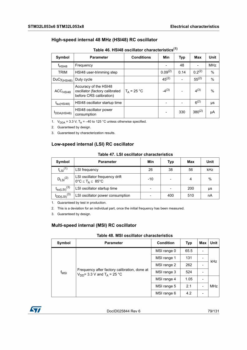
DocID025844 Rev 6 79/131
STM32L053x6 STM32L053x8 Electrical characteristics
112
High-speed internal 48 MHz (HSI48) RC oscillator
Low-speed internal (LSI) RC oscillator
Multi-speed internal (MSI) RC oscillator
Table 46. HSI48 oscillator characteristics(1)
1. VDDA = 3.3 V, TA = –40 to 125 °C unless otherwise specified.
Symbol Parameter Conditions Min Typ Max Unit
fHSI48 Frequency - 48 - MHz
TRIM HSI48 user-trimming step 0.09(2) 0.14 0.2(2) %
DuCy(HSI48) Duty cycle 45(2)
2. Guaranteed by design.
- 55(2) %
ACCHSI48
Accuracy of the HSI48 oscillator (factory calibrated before CRS calibration)
TA = 25 °C -4(3)
3. Guaranteed by characterization results.
- 4(3) %
tsu(HSI48) HSI48 oscillator startup time - - 6(2) µs
IDDA(HSI48)HSI48 oscillator power consumption
- 330 380(2) µA
Table 47. LSI oscillator characteristics
Symbol Parameter Min Typ Max Unit
fLSI(1)
1. Guaranteed by test in production.
LSI frequency 26 38 56 kHz
DLSI(2)
2. This is a deviation for an individual part, once the initial frequency has been measured.
LSI oscillator frequency drift0°C TA 85°C
-10 - 4 %
tsu(LSI)(3)
3. Guaranteed by design.
LSI oscillator startup time - - 200 µs
IDD(LSI)(3) LSI oscillator power consumption - 400 510 nA
Table 48. MSI oscillator characteristics
Symbol Parameter Condition Typ Max Unit
fMSIFrequency after factory calibration, done at VDD= 3.3 V and TA = 25 °C
MSI range 0 65.5 -
kHz MSI range 1 131 -
MSI range 2 262 -
MSI range 3 524 -
MSI range 4 1.05 -
MHzMSI range 5 2.1 -
MSI range 6 4.2 -

Electrical characteristics STM32L053x6 STM32L053x8
80/131 DocID025844 Rev 6
ACCMSI Frequency error after factory calibration - 0.5 - %
DTEMP(MSI)(1)
MSI oscillator frequency drift0 °C TA 85 °C
- 3 -
%MSI oscillator frequency driftVDD = 3.3 V, − 40 °C TA 110 °C
MSI range 0 − 8.9 +7.0
MSI range 1 − 7.1 +5.0
MSI range 2 − 6.4 +4.0
MSI range 3 − 6.2 +3.0
MSI range 4 − 5.2 +3.0
MSI range 5 − 4.8 +2.0
MSI range 6 − 4.7 +2.0
DVOLT(MSI)(1) MSI oscillator frequency drift
1.65 V VDD 3.6 V, TA = 25 °C- - 2.5 %/V
IDD(MSI)(2) MSI oscillator power consumption
MSI range 0 0.75 -
µA
MSI range 1 1 -
MSI range 2 1.5 -
MSI range 3 2.5 -
MSI range 4 4.5 -
MSI range 5 8 -
MSI range 6 15 -
tSU(MSI) MSI oscillator startup time
MSI range 0 30 -
µs
MSI range 1 20 -
MSI range 2 15 -
MSI range 3 10 -
MSI range 4 6 -
MSI range 5 5 -
MSI range 6, Voltage range 1
and 23.5 -
MSI range 6, Voltage range 3
5 -
Table 48. MSI oscillator characteristics (continued)
Symbol Parameter Condition Typ Max Unit
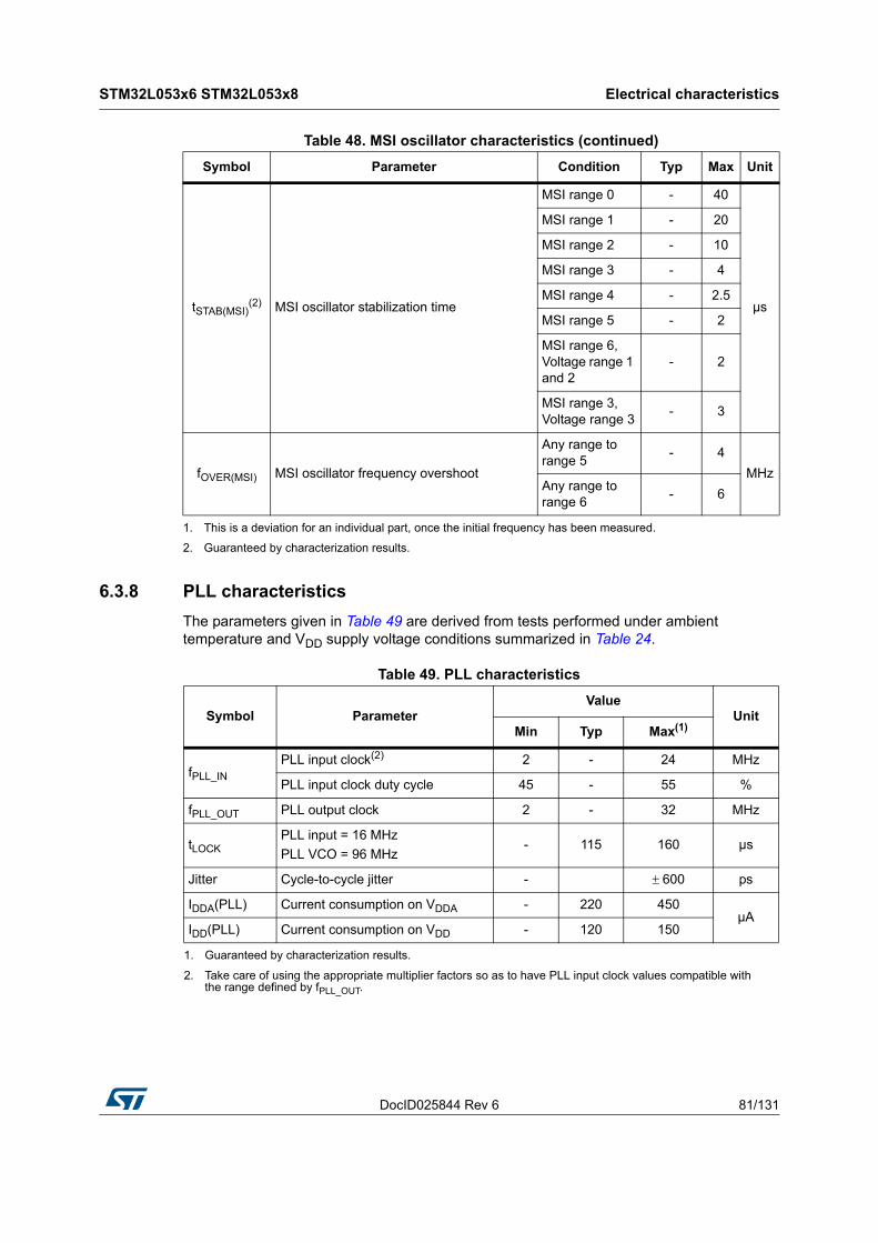
DocID025844 Rev 6 81/131
STM32L053x6 STM32L053x8 Electrical characteristics
112
6.3.8 PLL characteristics
The parameters given in Table 49 are derived from tests performed under ambient temperature and VDD supply voltage conditions summarized in Table 24.
tSTAB(MSI)(2) MSI oscillator stabilization time
MSI range 0 - 40
µs
MSI range 1 - 20
MSI range 2 - 10
MSI range 3 - 4
MSI range 4 - 2.5
MSI range 5 - 2
MSI range 6, Voltage range 1 and 2
- 2
MSI range 3, Voltage range 3
- 3
fOVER(MSI) MSI oscillator frequency overshoot
Any range to range 5
- 4
MHzAny range to range 6
- 6
1. This is a deviation for an individual part, once the initial frequency has been measured.
2. Guaranteed by characterization results.
Table 48. MSI oscillator characteristics (continued)
Symbol Parameter Condition Typ Max Unit
Table 49. PLL characteristics
Symbol ParameterValue
UnitMin Typ Max(1)
1. Guaranteed by characterization results.
fPLL_IN
PLL input clock(2)
2. Take care of using the appropriate multiplier factors so as to have PLL input clock values compatible with the range defined by fPLL_OUT.
2 - 24 MHz
PLL input clock duty cycle 45 - 55 %
fPLL_OUT PLL output clock 2 - 32 MHz
tLOCKPLL input = 16 MHz
PLL VCO = 96 MHz- 115 160 µs
Jitter Cycle-to-cycle jitter - 600 ps
IDDA(PLL) Current consumption on VDDA - 220 450µA
IDD(PLL) Current consumption on VDD - 120 150

Electrical characteristics STM32L053x6 STM32L053x8
82/131 DocID025844 Rev 6
6.3.9 Memory characteristics
RAM memory
Flash memory and data EEPROM
Table 50. RAM and hardware registers
Symbol Parameter Conditions Min Typ Max Unit
VRM Data retention mode(1)
1. Minimum supply voltage without losing data stored in RAM (in Stop mode or under Reset) or in hardware registers (only in Stop mode).
STOP mode (or RESET) 1.65 - - V
Table 51. Flash memory and data EEPROM characteristics
Symbol Parameter Conditions Min Typ Max(1)
1. Guaranteed by design.
Unit
VDDOperating voltage
Read / Write / Erase- 1.65 - 3.6 V
tprogProgramming time for word or half-page
Erasing - 3.28 3.94ms
Programming - 3.28 3.94
IDD
Average current during the whole programming / erase operation
TA25 °C, VDD = 3.6 V
- 500 700 µA
Maximum current (peak) during the whole programming / erase operation
- 1.5 2.5 mA
Table 52. Flash memory and data EEPROM endurance and retention
Symbol Parameter ConditionsValue
UnitMin(1)
NCYC(2)
Cycling (erase / write)Program memory
TA-40°C to 105 °C
10
kcycles
Cycling (erase / write)EEPROM data memory 100
Cycling (erase / write)Program memory
TA-40°C to 125 °C
0.2
Cycling (erase / write)EEPROM data memory
2

DocID025844 Rev 6 83/131
STM32L053x6 STM32L053x8 Electrical characteristics
112
6.3.10 EMC characteristics
Susceptibility tests are performed on a sample basis during device characterization.
Functional EMS (electromagnetic susceptibility)
While a simple application is executed on the device (toggling 2 LEDs through I/O ports). the device is stressed by two electromagnetic events until a failure occurs. The failure is indicated by the LEDs:
Electrostatic discharge (ESD) (positive and negative) is applied to all device pins until a functional disturbance occurs. This test is compliant with the IEC 61000-4-2 standard.
FTB: A Burst of Fast Transient voltage (positive and negative) is applied to VDD and VSS through a 100 pF capacitor, until a functional disturbance occurs. This test is compliant with the IEC 61000-4-4 standard.
A device reset allows normal operations to be resumed.
The test results are given in Table 53. They are based on the EMS levels and classes defined in application note AN1709.
tRET(2)
Data retention (program memory) after 10 kcycles at TA = 85 °C
TRET = +85 °C
30
years
Data retention (EEPROM data memory) after 100 kcycles at TA = 85 °C
30
Data retention (program memory) after 10 kcycles at TA = 105 °C
TRET = +105 °C
10
Data retention (EEPROM data memory) after 100 kcycles at TA = 105 °C
Data retention (program memory) after 200 cycles at TA = 125 °C
TRET = +125 °CData retention (EEPROM data memory) after 2 kcycles at TA = 125 °C
1. Guaranteed by characterization results.
2. Characterization is done according to JEDEC JESD22-A117.
Table 52. Flash memory and data EEPROM endurance and retention (continued)
Symbol Parameter ConditionsValue
UnitMin(1)
Table 53. EMS characteristics
Symbol Parameter ConditionsLevel/Class
VFESDVoltage limits to be applied on any I/O pin to induce a functional disturbance
VDD 3.3 V, LQFP64, TA +25 °C, fHCLK 32 MHzconforms to IEC 61000-4-2
3B
VEFTB
Fast transient voltage burst limits to be applied through 100 pF on VDD and VSS pins to induce a functional disturbance
VDD3.3 V, LQFP64, TA +25 °C, fHCLK 32 MHzconforms to IEC 61000-4-4
4A

Electrical characteristics STM32L053x6 STM32L053x8
84/131 DocID025844 Rev 6
Designing hardened software to avoid noise problems
EMC characterization and optimization are performed at component level with a typical application environment and simplified MCU software. It should be noted that good EMC performance is highly dependent on the user application and the software in particular.
Therefore it is recommended that the user applies EMC software optimization and prequalification tests in relation with the EMC level requested for his application.
Software recommendations
The software flowchart must include the management of runaway conditions such as:
Corrupted program counter
Unexpected reset
Critical data corruption (control registers...)
Prequalification trials
Most of the common failures (unexpected reset and program counter corruption) can be reproduced by manually forcing a low state on the NRST pin or the oscillator pins for 1 second.
To complete these trials, ESD stress can be applied directly on the device, over the range of specification values. When unexpected behavior is detected, the software can be hardened to prevent unrecoverable errors occurring (see application note AN1015).
Electromagnetic Interference (EMI)
The electromagnetic field emitted by the device are monitored while a simple application is executed (toggling 2 LEDs through the I/O ports). This emission test is compliant with IEC 61967-2 standard which specifies the test board and the pin loading.
Table 54. EMI characteristics
Symbol Parameter ConditionsMonitored
frequency band
Max vs. fosc/fCPU
Unit8 MHz/4 MHz
8 MHz/16 MHz
8 MHz/32 MHz
SEMI Peak level
VDD 3.6 V,
TA 25 °C,compliant with IEC 61967-2
0.1 to 30 MHz -21 -15 -12
dBµV30 to 130 MHz -14 -12 -1
130 MHz to 1GHz -10 -11 -7
EMI Level 1 1 1 -

DocID025844 Rev 6 85/131
STM32L053x6 STM32L053x8 Electrical characteristics
112
6.3.11 Electrical sensitivity characteristics
Based on three different tests (ESD, LU) using specific measurement methods, the device is stressed in order to determine its performance in terms of electrical sensitivity.
Electrostatic discharge (ESD)
Electrostatic discharges (a positive then a negative pulse separated by 1 second) are applied to the pins of each sample according to each pin combination. The sample size depends on the number of supply pins in the device (3 parts × (n+1) supply pins). This test conforms to the ANSI/JEDEC standard.
Static latch-up
Two complementary static tests are required on six parts to assess the latch-up performance:
A supply overvoltage is applied to each power supply pin
A current injection is applied to each input, output and configurable I/O pin
These tests are compliant with EIA/JESD 78A IC latch-up standard.
Table 55. ESD absolute maximum ratings
Symbol Ratings Conditions ClassMaximum value(1)
1. Guaranteed by characterization results.
Unit
VESD(HBM)Electrostatic discharge voltage (human body model)
TA +25 °C, conforming to ANSI/JEDEC JS-001
2 2000
V
VESD(CDM)
Electrostatic discharge voltage (charge device model)
TA +25 °C, conforming to ANSI/ESD STM5.3.1.
C4 500
Table 56. Electrical sensitivities
Symbol Parameter Conditions Class
LU Static latch-up class TA +125 °C conforming to JESD78A II level A

Electrical characteristics STM32L053x6 STM32L053x8
86/131 DocID025844 Rev 6
6.3.12 I/O current injection characteristics
As a general rule, current injection to the I/O pins, due to external voltage below VSS or above VDD (for standard pins) should be avoided during normal product operation. However, in order to give an indication of the robustness of the microcontroller in cases when abnormal injection accidentally happens, susceptibility tests are performed on a sample basis during device characterization.
Functional susceptibility to I/O current injection
While a simple application is executed on the device, the device is stressed by injecting current into the I/O pins programmed in floating input mode. While current is injected into the I/O pin, one at a time, the device is checked for functional failures.
The failure is indicated by an out of range parameter: ADC error above a certain limit (higher than 5 LSB TUE), out of conventional limits of induced leakage current on adjacent pins (out of –5 µA/+0 µA range), or other functional failure (for example reset occurrence oscillator frequency deviation, LCD levels).
The test results are given in the Table 57.
Table 57. I/O current injection susceptibility
Symbol Description
Functional susceptibility
UnitNegative injection
Positive injection
IINJ
Injected current on BOOT0 -0 NA
mA
Injected current on PA0, PA4, PA5, PA11, PA12, PC15, PH0 and PH1
-5 0
Injected current on any other FT, FTf pins -5 (1)
1. It is recommended to add a Schottky diode (pin to ground) to analog pins which may potentially inject negative currents.
NA
Injected current on any other pins -5 (1) +5

DocID025844 Rev 6 87/131
STM32L053x6 STM32L053x8 Electrical characteristics
112
6.3.13 I/O port characteristics
General input/output characteristics
Unless otherwise specified, the parameters given in Table 58 are derived from tests performed under the conditions summarized in Table 24. All I/Os are CMOS and TTL compliant.
Table 58. I/O static characteristics
Symbol Parameter Conditions Min Typ Max Unit
VIL Input low level voltage
TC, FT, FTf, RST I/Os
- - 0.3VDD
V BOOT0 pin - - 0.14VDD
(1)
VIH Input high level voltage All I/Os 0.7 VDD - -
VhysI/O Schmitt trigger voltage hysteresis (2)
Standard I/Os - 10% VDD(3) -
BOOT0 pin - 0.01 -
Ilkg Input leakage current (4)
VSS VIN VDDAll I/Os except for
PA11, PA12, BOOT0 and FTf I/Os
- - ±50
nAVSS VIN VDD,
PA11 and PA12 I/Os- - -50/+250
VSS VIN VDDFTf I/Os
- - ±100
VDDVIN 5 V
All I/Os except for PA11, PA12, BOOT0
and FTf I/Os
- - 200
nA
VDDVIN 5 V
FTf I/Os- - 500
VDDVIN 5 V
PA11, PA12 and BOOT0
- - 10 µA
RPU Weak pull-up equivalent resistor(5) VIN VSS 30 45 60 k
RPD Weak pull-down equivalent resistor(5) VIN VDD 30 45 60 k
CIO I/O pin capacitance - - 5 - pF
1. Guaranteed by characterization.
2. Hysteresis voltage between Schmitt trigger switching levels. Guaranteed by characterization results.
3. With a minimum of 200 mV. Guaranteed by characterization results.
4. The max. value may be exceeded if negative current is injected on adjacent pins.
5. Pull-up and pull-down resistors are designed with a true resistance in series with a switchable PMOS/NMOS. This MOS/NMOS contribution to the series resistance is minimum (~10% order).

Electrical characteristics STM32L053x6 STM32L053x8
88/131 DocID025844 Rev 6
Figure 22. VIH/VIL versus VDD (CMOS I/Os)
Figure 23. VIH/VIL versus VDD (TTL I/Os)
Output driving current
The GPIOs (general purpose input/outputs) can sink or source up to ±8 mA, and sink or source up to ±15 mA with the non-standard VOL/VOH specifications given in Table 59.
In the user application, the number of I/O pins which can drive current must be limited to respect the absolute maximum rating specified in Section 6.2:
The sum of the currents sourced by all the I/Os on VDD, plus the maximum Run consumption of the MCU sourced on VDD, cannot exceed the absolute maximum rating IVDD(Σ) (see Table 22).
The sum of the currents sunk by all the I/Os on VSS plus the maximum Run consumption of the MCU sunk on VSS cannot exceed the absolute maximum rating IVSS(Σ) (see Table 22).

DocID025844 Rev 6 89/131
STM32L053x6 STM32L053x8 Electrical characteristics
112
Output voltage levels
Unless otherwise specified, the parameters given in Table 59 are derived from tests performed under ambient temperature and VDD supply voltage conditions summarized in Table 24. All I/Os are CMOS and TTL compliant.
Table 59. Output voltage characteristics
Symbol Parameter Conditions Min Max Unit
VOL(1)
1. The IIO current sunk by the device must always respect the absolute maximum rating specified in Table 22. The sum of the currents sunk by all the I/Os (I/O ports and control pins) must always be respected and must not exceed ΣIIO(PIN).
Output low level voltage for an I/O pin CMOS port(2),
IIO = +8 mA2.7 V VDD 3.6 V
2. TTL and CMOS outputs are compatible with JEDEC standards JESD36 and JESD52.
- 0.4
V
VOH(3)
3. The IIO current sourced by the device must always respect the absolute maximum rating specified in Table 22. The sum of the currents sourced by all the I/Os (I/O ports and control pins) must always be respected and must not exceed ΣIIO(PIN).
Output high level voltage for an I/O pin
VDD-0.4 -
VOL (1) Output low level voltage for an I/O
pin
TTL port(2), IIO =+ 8 mA
2.7 V VDD 3.6 V- 0.4
VOH (3)(4)
4. Guaranteed by characterization results.
Output high level voltage for an I/O pin
TTL port(2), IIO = -6 mA
2.7 V VDD 3.6 V2.4 -
VOL(1)(4) Output low level voltage for an I/O
pinIIO = +15 mA
2.7 V VDD 3.6 V- 1.3
VOH(3)(4) Output high level voltage for an I/O
pinIIO = -15 mA
2.7 V VDD 3.6 VVDD-1.3 -
VOL(1)(4) Output low level voltage for an I/O
pinIIO = +4 mA
1.65 V VDD < 3.6 V- 0.45
VOH(3)(4) Output high level voltage for an I/O
pinIIO = -4 mA
1.65 V VDD 3.6 VVDD-0.45 -
VOLFM+(1)(4) Output low level voltage for an FTf
I/O pin in Fm+ mode
IIO = 20 mA2.7 V VDD 3.6 V
- 0.4
IIO = 10 mA1.65 V VDD 3.6 V
- 0.4

Electrical characteristics STM32L053x6 STM32L053x8
90/131 DocID025844 Rev 6
Input/output AC characteristics
The definition and values of input/output AC characteristics are given in Figure 24 and Table 60, respectively.
Unless otherwise specified, the parameters given in Table 60 are derived from tests performed under ambient temperature and VDD supply voltage conditions summarized in Table 24.
Table 60. I/O AC characteristics(1)
OSPEEDRx[1:0] bit value(1) Symbol Parameter Conditions Min Max(2) Unit
00
fmax(IO)out Maximum frequency(3)CL = 50 pF, VDD = 2.7 V to 3.6 V - 400
kHzCL = 50 pF, VDD = 1.65 V to 2.7 V - 100
tf(IO)outtr(IO)out
Output rise and fall timeCL = 50 pF, VDD = 2.7 V to 3.6 V - 125
nsCL = 50 pF, VDD = 1.65 V to 2.7 V - 320
01
fmax(IO)out Maximum frequency(3)CL = 50 pF, VDD = 2.7 V to 3.6 V - 2
MHzCL = 50 pF, VDD = 1.65 V to 2.7 V - 0.6
tf(IO)outtr(IO)out
Output rise and fall timeCL = 50 pF, VDD = 2.7 V to 3.6 V - 30
nsCL = 50 pF, VDD = 1.65 V to 2.7 V - 65
10
Fmax(IO)out Maximum frequency(3)CL = 50 pF, VDD = 2.7 V to 3.6 V - 10
MHzCL = 50 pF, VDD = 1.65 V to 2.7 V - 2
tf(IO)outtr(IO)out
Output rise and fall timeCL = 50 pF, VDD = 2.7 V to 3.6 V - 13
nsCL = 50 pF, VDD = 1.65 V to 2.7 V - 28
11
Fmax(IO)out Maximum frequency(3)CL = 30 pF, VDD = 2.7 V to 3.6 V - 35
MHzCL = 50 pF, VDD = 1.65 V to 2.7 V - 10
tf(IO)outtr(IO)out
Output rise and fall timeCL = 30 pF, VDD = 2.7 V to 3.6 V - 6
nsCL = 50 pF, VDD = 1.65 V to 2.7 V - 17
Fm+ configuration(4)
fmax(IO)out Maximum frequency(3)
CL = 50 pF, VDD = 2.5 V to 3.6 V
- 1 MHz
tf(IO)out Output fall time - 10ns
tr(IO)out Output rise time - 30
fmax(IO)out Maximum frequency(3)
CL = 50 pF, VDD = 1.65 V to 3.6 V
- 350 KHz
tf(IO)out Output fall time - 15ns
tr(IO)out Output rise time - 60
- tEXTIpw
Pulse width of external signals detected by the EXTI controller
- 8 - ns
1. The I/O speed is configured using the OSPEEDRx[1:0] bits. Refer to the line reference manual for a description of GPIO Port configuration register.
2. Guaranteed by design.
3. The maximum frequency is defined in Figure 24.
4. When Fm+ configuration is set, the I/O speed control is bypassed. Refer to the line reference manual for a detailed description of Fm+ I/O configuration.

DocID025844 Rev 6 91/131
STM32L053x6 STM32L053x8 Electrical characteristics
112
Figure 24. I/O AC characteristics definition
6.3.14 NRST pin characteristics
The NRST pin input driver uses CMOS technology. It is connected to a permanent pull-up resistor, RPU , except when it is internally driven low (see Table 61).
Unless otherwise specified, the parameters given in Table 61 are derived from tests performed under ambient temperature and VDD supply voltage conditions summarized in Table 24.
Table 61. NRST pin characteristics
Symbol Parameter Conditions Min Typ Max Unit
VIL(NRST)(1)
1. Guaranteed by design.
NRST input low level voltage - VSS - 0.8
V
VIH(NRST)(1) NRST input high level voltage - 1.4 - VDD
VOL(NRST)(1) NRST output low level
voltage
IOL = 2 mA2.7 V < VDD < 3.6 V
- -
0.4IOL = 1.5 mA
1.65 V < VDD < 2.7 V- -
Vhys(NRST)(1) NRST Schmitt trigger voltage
hysteresis - - 10%VDD
(2)
2. 200 mV minimum value
- mV
RPUWeak pull-up equivalent resistor(3)
3. The pull-up is designed with a true resistance in series with a switchable PMOS. This PMOS contribution to the series resistance is around 10%.
VIN VSS 30 45 60 k
VF(NRST)(1) NRST input filtered pulse - - - 50 ns
VNF(NRST)(1) NRST input not filtered pulse - 350 - - ns

Electrical characteristics STM32L053x6 STM32L053x8
92/131 DocID025844 Rev 6
Figure 25. Recommended NRST pin protection
1. The reset network protects the device against parasitic resets.
2. The user must ensure that the level on the NRST pin can go below the VIL(NRST) max level specified in Table 61. Otherwise the reset will not be taken into account by the device.
6.3.15 12-bit ADC characteristics
Unless otherwise specified, the parameters given in Table 62 are derived from tests performed under ambient temperature, fPCLK frequency and VDDA supply voltage conditions summarized in Table 24: General operating conditions.
Note: It is recommended to perform a calibration after each power-up.
Table 62. ADC characteristics
Symbol Parameter Conditions Min Typ Max Unit
VDDAAnalog supply voltage for ADC on
Fast channel 1.65 - 3.6V
Standard channel 1.75(1) - 3.6
VREF+ Positive reference voltage - 1.65 VDDA V
IDDA (ADC)
Current consumption of the ADC on VDDA and VREF+
1.14 Msps - 200 -
µA10 ksps - 40 -
Current consumption of the ADC on VDD
(2)
1.14 Msps - 70 -
10 ksps - 1 -
fADC ADC clock frequency
Voltage scaling Range 1 0.14 - 16
MHzVoltage scaling Range 2 0.14 - 8
Voltage scaling Range 3 0.14 - 4
fS(3) Sampling rate 12-bit resolution 0.01 - 1.14 MHz
fTRIG(3) External trigger frequency
fADC = 16 MHz, 12-bit resolution
- - 941 kHz
- - - 17 1/fADC
VAIN Conversion voltage range - 0 - VREF+ V
RAIN(3) External input impedance
See Equation 1 and Table 63 for details
- - 50 k
RADC(3)(4) Sampling switch resistance - - - 1 k

DocID025844 Rev 6 93/131
STM32L053x6 STM32L053x8 Electrical characteristics
112
CADC(3) Internal sample and hold
capacitor- - - 8 pF
tCAL(3)(5) Calibration time
fADC = 16 MHz 5.2 µs
- 83 1/fADC
WLATENCY(6) ADC_DR register write
latency
ADC clock = HSI161.5 ADC
cycles + 2 fPCLK cycles
-1.5 ADC
cycles + 3 fPCLK cycles
-
ADC clock = PCLK/2 - 4.5 -fPCLK
cycle
ADC clock = PCLK/4 - 8.5 -fPCLK
cycle
tlatr(3) Trigger conversion latency
fADC = fPCLK/2 = 16 MHz 0.266 µs
fADC = fPCLK/2 8.5 1/fPCLK
fADC = fPCLK/4 = 8 MHz 0.516 µs
fADC = fPCLK/4 16.5 1/fPCLK
fADC = fHSI16 = 16 MHz 0.252 - 0.260 µs
JitterADCADC jitter on trigger conversion
fADC = fHSI16 - 1 - 1/fHSI16
tS(3) Sampling time
fADC = 16 MHz 0.093 - 10.03 µs
- 1.5 - 160.5 1/fADC
tUP_LDO(3)(5) Internal LDO power-up time - - - 10 µs
tSTAB(3)(5) ADC stabilization time - 14 1/fADC
tConV(3) Total conversion time
(including sampling time)
fADC = 16 MHz,12-bit resolution
0.875 - 10.81 µs
12-bit resolution14 to 173 (tS for sampling +12.5 for successive approximation)
1/fADC
1. VDDA minimum value can be decreased in specific temperature conditions. Refer to Table 63: RAIN max for fADC = 16 MHz.
2. A current consumption proportional to the APB clock frequency has to be added (see Table 38: Peripheral current consumption in Run or Sleep mode).
3. Guaranteed by design.
4. Standard channels have an extra protection resistance which depends on supply voltage. Refer to Table 63: RAIN max for fADC = 16 MHz.
5. This parameter only includes the ADC timing. It does not take into account register access latency.
6. This parameter specifies the latency to transfer the conversion result into the ADC_DR register. EOC bit is set to indicate the conversion is complete and has the same latency.
Table 62. ADC characteristics (continued)
Symbol Parameter Conditions Min Typ Max Unit

Electrical characteristics STM32L053x6 STM32L053x8
94/131 DocID025844 Rev 6
Equation 1: RAIN max formula
The simplified formula above (Equation 1) is used to determine the maximum external impedance allowed for an error below 1/4 of LSB. Here N = 12 (from 12-bit resolution).
RAIN
TS
fADC CADC 2N 2+ ln
-------------------------------------------------------------- RADC–
Table 63. RAIN max for fADC = 16 MHz(1)
Ts (cycles)
tS (µs)
RAIN max for fast channels
(k)
RAIN max for standard channels (k)
VDD > 2.7 V
VDD > 2.4 V
VDD > 2.0 V
VDD > 1.8 V
VDD > 1.75 V
VDD > 1.65 V and
TA > 10 °C
VDD > 1.65 V and
TA > 25 °C
1.5 0.09 0.5 < 0.1 NA NA NA NA NA NA
3.5 0.22 1 0.2 < 0.1 NA NA NA NA NA
7.5 0.47 2.5 1.7 1.5 < 0.1 NA NA NA NA
12.5 0.78 4 3.2 3 1 NA NA NA NA
19.5 1.22 6.5 5.7 5.5 3.5 NA NA NA < 0.1
39.5 2.47 13 12.2 12 10 NA NA NA 5
79.5 4.97 27 26.2 26 24 < 0.1 NA NA 19
160.5 10.03 50 49.2 49 47 32 < 0.1 < 0.1 42
1. Guaranteed by design.
Table 64. ADC accuracy(1)(2)(3)
Symbol Parameter Conditions Min Typ Max Unit
ET Total unadjusted error
1.65 V < VDDA = VREF+ < 3.6 V, range 1/2/3
- 2 4
LSB
EO Offset error - 1 2.5
EG Gain error - 1 2
EL Integral linearity error - 1.5 2.5
ED Differential linearity error - 1 1.5
ENOB
Effective number of bits 10.2 11
bitsEffective number of bits (16-bit mode oversampling with ratio =256)(4) 11.3 12.1 -
SINAD Signal-to-noise distortion 63 69 -
dBSNR
Signal-to-noise ratio 63 69 -
Signal-to-noise ratio (16-bit mode oversampling with ratio =256)(4) 70 76 -
THD Total harmonic distortion - -85 -73

DocID025844 Rev 6 95/131
STM32L053x6 STM32L053x8 Electrical characteristics
112
Figure 26. ADC accuracy characteristics
ET Total unadjusted error
1.65 V < VREF+ < VDDA < 3.6 V,range 1/2/3
- 2 5
LSB
EO Offset error - 1 2.5
EG Gain error - 1 2
EL Integral linearity error - 1.5 3
ED Differential linearity error - 1 2
ENOB Effective number of bits 10.0 11.0 - bits
SINAD Signal-to-noise distortion 62 69 -
dBSNR Signal-to-noise ratio 61 69 -
THD Total harmonic distortion - -85 -65
1. ADC DC accuracy values are measured after internal calibration.
2. ADC Accuracy vs. Negative Injection Current: Injecting negative current on any of the standard (non-robust) analog input pins should be avoided as this significantly reduces the accuracy of the conversion being performed on another analog input. It is recommended to add a Schottky diode (pin to ground) to standard analog pins which may potentially inject negative current. Any positive injection current within the limits specified for IINJ(PIN) and IINJ(PIN) in Section 6.3.12 does not affect the ADC accuracy.
3. Better performance may be achieved in restricted VDDA, frequency and temperature ranges.
4. This number is obtained by the test board without additional noise, resulting in non-optimized value for oversampling mode.
Table 64. ADC accuracy(1)(2)(3)
Symbol Parameter Conditions Min Typ Max Unit

Electrical characteristics STM32L053x6 STM32L053x8
96/131 DocID025844 Rev 6
Figure 27. Typical connection diagram using the ADC
1. Refer to Table 62: ADC characteristics for the values of RAIN, RADC and CADC.
2. Cparasitic represents the capacitance of the PCB (dependent on soldering and PCB layout quality) plus the pad capacitance (roughly 7 pF). A high Cparasitic value will downgrade conversion accuracy. To remedy this, fADC should be reduced.
General PCB design guidelines
Power supply decoupling should be performed as shown in Figure 28 or Figure 29, depending on whether VREF+ is connected to VDDA or not. The 10 nF capacitors should be ceramic (good quality). They should be placed as close as possible to the chip.
Figure 28. Power supply and reference decoupling (VREF+ not connected to VDDA)
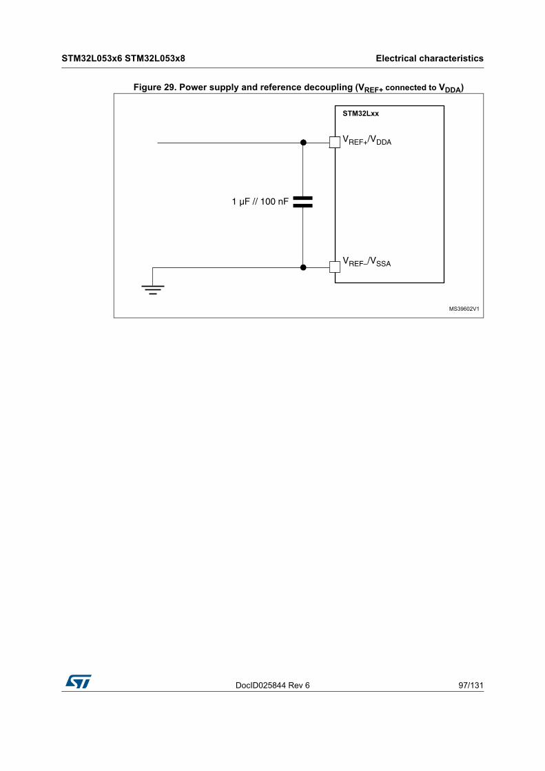
DocID025844 Rev 6 97/131
STM32L053x6 STM32L053x8 Electrical characteristics
112
Figure 29. Power supply and reference decoupling (VREF+ connected to VDDA)
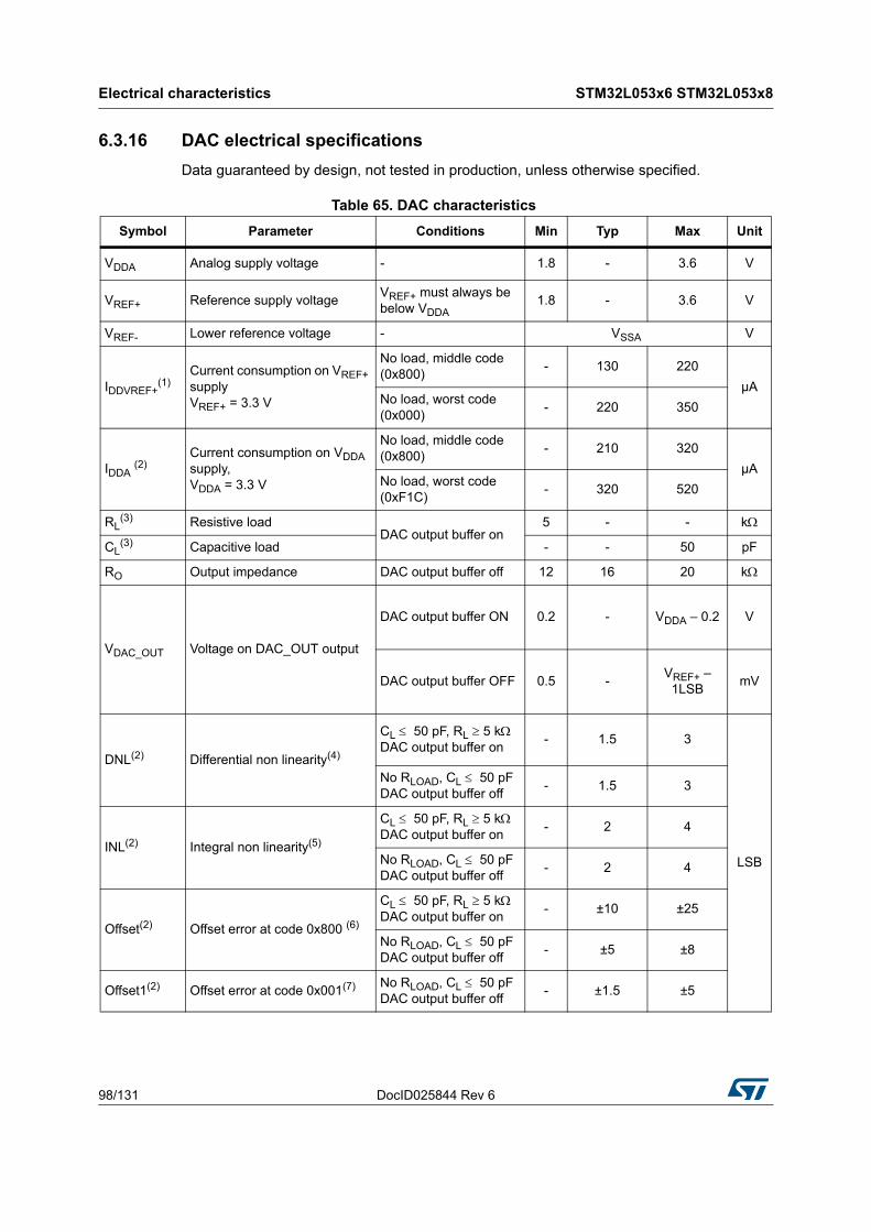
Electrical characteristics STM32L053x6 STM32L053x8
98/131 DocID025844 Rev 6
6.3.16 DAC electrical specifications
Data guaranteed by design, not tested in production, unless otherwise specified.
Table 65. DAC characteristics
Symbol Parameter Conditions Min Typ Max Unit
VDDA Analog supply voltage - 1.8 - 3.6 V
VREF+ Reference supply voltageVREF+ must always be below VDDA
1.8 - 3.6 V
VREF- Lower reference voltage - VSSA V
IDDVREF+(1)
Current consumption on VREF+ supplyVREF+ = 3.3 V
No load, middle code (0x800)
- 130 220
µANo load, worst code (0x000)
- 220 350
IDDA (2)Current consumption on VDDA supply, VDDA = 3.3 V
No load, middle code (0x800)
- 210 320
µANo load, worst code (0xF1C)
- 320 520
RL(3) Resistive load
DAC output buffer on5 - - k
CL(3) Capacitive load - - 50 pF
RO Output impedance DAC output buffer off 12 16 20 k
VDAC_OUT Voltage on DAC_OUT output
DAC output buffer ON 0.2 - VDDA – 0.2 V
DAC output buffer OFF 0.5 -VREF+ –
1LSBmV
DNL(2) Differential non linearity(4)
CL 50 pF, RL 5 kDAC output buffer on
- 1.5 3
LSB
No RLOAD, CL 50 pFDAC output buffer off
- 1.5 3
INL(2) Integral non linearity(5)
CL 50 pF, RL 5 kDAC output buffer on
- 2 4
No RLOAD, CL 50 pFDAC output buffer off
- 2 4
Offset(2) Offset error at code 0x800 (6)
CL 50 pF, RL 5 kDAC output buffer on
- ±10 ±25
No RLOAD, CL 50 pFDAC output buffer off
- ±5 ±8
Offset1(2) Offset error at code 0x001(7) No RLOAD, CL 50 pFDAC output buffer off
- ±1.5 ±5

DocID025844 Rev 6 99/131
STM32L053x6 STM32L053x8 Electrical characteristics
112
dOffset/dT(2) Offset error temperature coefficient (code 0x800)
VDDA 3.3V
VREF+3.0 V
TA = 0 to 50 CDAC output buffer off
-20 -10 0
µV/°CVDDA 3.3V
VREF+3.0 V
TA = 0 to 50 CDAC output buffer on
0 20 50
Gain(2) Gain error(8)
CL 50 pF, RL 5 kDAC output buffer on
- +0.1 / -0.2% +0.2 / -0.5%
%No RLOAD, CL 50 pFDAC output buffer off
- +0 / -0.2% +0 / -0.4%
dGain/dT(2) Gain error temperature coefficient
VDDA 3.3V
VREF+3.0 V
TA = 0 to 50 CDAC output buffer off
-10 -2 0
µV/°CVDDA 3.3V
VREF+3.0 V
TA = 0 to 50 CDAC output buffer on
-40 -8 0
TUE(2) Total unadjusted error
CL 50 pF, RL 5 kDAC output buffer on
- 12 30
LSBNo RLOAD, CL 50 pFDAC output buffer off
- 8 12
tSETTLING
Settling time (full scale: for a 12-bit code transition between the lowest and the highest input codes till DAC_OUT reaches final value ±1LSB
CL 50 pF, RL 5 k - 7 12 µs
Update rate
Max frequency for a correct DAC_OUT change (95% of final value) with 1 LSB variation in the input code
CL 50 pF, RL 5 k - - 1 Msps
tWAKEUP
Wakeup time from off state (setting the ENx bit in the DAC Control register)(9)
CL 50 pF, RL 5 k - 9 15 µs
PSRR+VDDA supply rejection ratio (static DC measurement)
CL 50 pF, RL 5 k - -60 -35 dB
1. Guaranteed by characterization results.
2. Guaranteed by design, not tested in production.
3. Connected between DAC_OUT and VSSA.
4. Difference between two consecutive codes - 1 LSB.
5. Difference between measured value at Code i and the value at Code i on a line drawn between Code 0 and last Code 4095.
Table 65. DAC characteristics (continued)
Symbol Parameter Conditions Min Typ Max Unit

Electrical characteristics STM32L053x6 STM32L053x8
100/131 DocID025844 Rev 6
Figure 30. 12-bit buffered/non-buffered DAC
6.3.17 Temperature sensor characteristics
6. Difference between the value measured at Code (0x800) and the ideal value = VREF+/2.
7. Difference between the value measured at Code (0x001) and the ideal value.
8. Difference between ideal slope of the transfer function and measured slope computed from code 0x000 and 0xFFF when buffer is off, and from code giving 0.2 V and (VDDA – 0.2) V when buffer is on.
9. In buffered mode, the output can overshoot above the final value for low input code (starting from min value).
Table 66. Temperature sensor calibration values
Calibration value name Description Memory address
TS_CAL1TS ADC raw data acquired at temperature of 30 °C, VDDA= 3 V
0x1FF8 007A - 0x1FF8 007B
TS_CAL2TS ADC raw data acquired at temperature of 130 °C, VDDA= 3 V
0x1FF8 007E - 0x1FF8 007F
Table 67. Temperature sensor characteristics
Symbol Parameter Min Typ Max Unit
TL(1)
1. Guaranteed by characterization results.
VSENSE linearity with temperature - 1 2 °C
Avg_Slope(1) Average slope 1.48 1.61 1.75 mV/°C
V130 Voltage at 130°C ±5°C(2)
2. Measured at VDD = 3 V ±10 mV. V130 ADC conversion result is stored in the TS_CAL2 byte.
640 670 700 mV
IDDA(TEMP)(3) Current consumption - 3.4 6 µA
tSTART(3)
3. Guaranteed by design.
Startup time - - 10µs
TS_temp(4)(3)
4. Shortest sampling time can be determined in the application by multiple iterations.
ADC sampling time when reading the temperature 10 - -

DocID025844 Rev 6 101/131
STM32L053x6 STM32L053x8 Electrical characteristics
112
6.3.18 Comparators
Table 68. Comparator 1 characteristics
Symbol Parameter Conditions Min(1) Typ Max(1) Unit
VDDA Analog supply voltage - 1.65 3.6 V
R400K R400K value - - 400 -k
R10K R10K value - - 10 -
VINComparator 1 input voltage range
- 0.6 - VDDA V
tSTART Comparator startup time - - 7 10µs
td Propagation delay(2) - - 3 10
Voffset Comparator offset - - 3 10 mV
dVoffset/dtComparator offset variation in worst voltage stress conditions
VDDA 3.6 V, VIN+ 0 V, VIN- VREFINT, TA = 25 C
0 1.5 10 mV/1000 h
ICOMP1 Current consumption(3) - - 160 260 nA
1. Guaranteed by characterization.
2. The delay is characterized for 100 mV input step with 10 mV overdrive on the inverting input, the non-inverting input set to the reference.
3. Comparator consumption only. Internal reference voltage not included.
Table 69. Comparator 2 characteristics
Symbol Parameter Conditions Min Typ Max(1) Unit
VDDA Analog supply voltage - 1.65 - 3.6 V
VIN Comparator 2 input voltage range - 0 - VDDA V
tSTART Comparator startup time Fast mode - 15 20
µs
Slow mode - 20 25
td slow Propagation delay(2) in slow mode1.65 V VDDA 2.7 V - 1.8 3.5
2.7 V VDDA 3.6 V - 2.5 6
td fast Propagation delay(2) in fast mode1.65 V VDDA 2.7 V - 0.8 2
2.7 V VDDA 3.6 V - 1.2 4
Voffset Comparator offset error - 4 20 mV
dThreshold/dt
Threshold voltage temperature coefficient
VDDA 3.3V, TA = 0 to 50 C, V- = VREFINT,3/4 VREFINT,1/2 VREFINT,1/4 VREFINT.
- 15 30ppm/°C
ICOMP2 Current consumption(3)Fast mode - 3.5 5
µASlow mode - 0.5 2
1. Guaranteed by characterization results.
2. The delay is characterized for 100 mV input step with 10 mV overdrive on the inverting input, the non-inverting input set to the reference.
3. Comparator consumption only. Internal reference voltage (required for comparator operation) is not included.
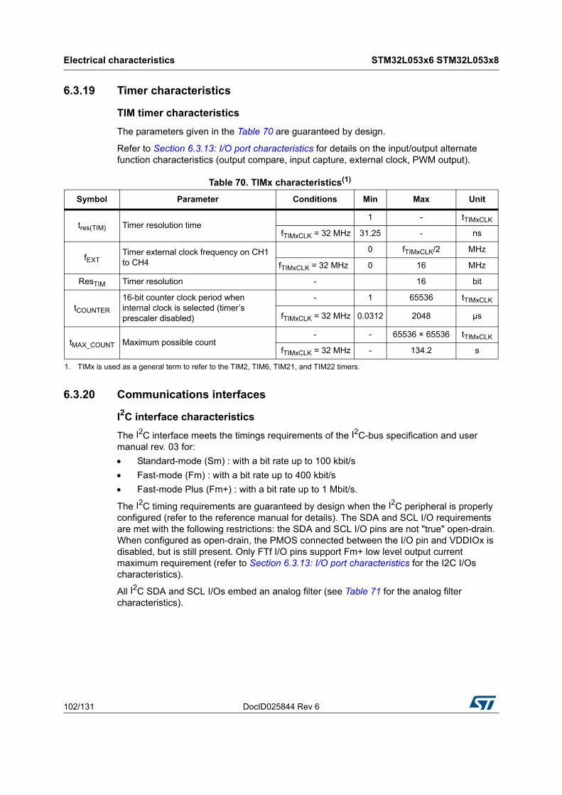
Electrical characteristics STM32L053x6 STM32L053x8
102/131 DocID025844 Rev 6
6.3.19 Timer characteristics
TIM timer characteristics
The parameters given in the Table 70 are guaranteed by design.
Refer to Section 6.3.13: I/O port characteristics for details on the input/output alternate function characteristics (output compare, input capture, external clock, PWM output).
6.3.20 Communications interfaces
I2C interface characteristics
The I2C interface meets the timings requirements of the I2C-bus specification and user manual rev. 03 for:
Standard-mode (Sm) : with a bit rate up to 100 kbit/s
Fast-mode (Fm) : with a bit rate up to 400 kbit/s
Fast-mode Plus (Fm+) : with a bit rate up to 1 Mbit/s.
The I2C timing requirements are guaranteed by design when the I2C peripheral is properly configured (refer to the reference manual for details). The SDA and SCL I/O requirements are met with the following restrictions: the SDA and SCL I/O pins are not "true" open-drain. When configured as open-drain, the PMOS connected between the I/O pin and VDDIOx is disabled, but is still present. Only FTf I/O pins support Fm+ low level output current maximum requirement (refer to Section 6.3.13: I/O port characteristics for the I2C I/Os characteristics).
All I2C SDA and SCL I/Os embed an analog filter (see Table 71 for the analog filter characteristics).
Table 70. TIMx characteristics(1)
Symbol Parameter Conditions Min Max Unit
tres(TIM) Timer resolution time1 - tTIMxCLK
fTIMxCLK = 32 MHz 31.25 - ns
fEXTTimer external clock frequency on CH1 to CH4
0 fTIMxCLK/2 MHz
fTIMxCLK = 32 MHz 0 16 MHz
ResTIM Timer resolution - 16 bit
tCOUNTER
16-bit counter clock period when internal clock is selected (timer’s prescaler disabled)
- 1 65536 tTIMxCLK
fTIMxCLK = 32 MHz 0.0312 2048 µs
tMAX_COUNT Maximum possible count- - 65536 × 65536 tTIMxCLK
fTIMxCLK = 32 MHz - 134.2 s
1. TIMx is used as a general term to refer to the TIM2, TIM6, TIM21, and TIM22 timers.

DocID025844 Rev 6 103/131
STM32L053x6 STM32L053x8 Electrical characteristics
112
The analog spike filter is compliant with I2C timings requirements only for the following voltage ranges:
Fast mode Plus: 2.7 V VDD 3.6 V and voltage scaling Range 1
Fast mode:
– 2 V VDD 3.6 V and voltage scaling Range 1 or Range 2.
– VDD < 2 V, voltage scaling Range 1 or Range 2, Cload < 200 pF.
In other ranges, the analog filter should be disabled. The digital filter can be used instead.
Note: In Standard mode, no spike filter is required.
USART/LPUART characteristics
The parameters given in the following table are guaranteed by design.
Table 71. I2C analog filter characteristics(1)
1. Guaranteed by characterization results.
Symbol Parameter Conditions Min Max Unit
tAFMaximum pulse width of spikes that are suppressed by the analog filter
Range 1
50(2)
2. Spikes with widths below tAF(min) are filtered.
100(3)
3. Spikes with widths above tAF(max) are not filtered
nsRange 2 -
Range 3 -
Table 72. USART/LPUART characteristics
Symbol Parameter Conditions Typ Max Unit
tWUUSART
Wakeup time needed to calculate the maximum
USART/LPUART baudrate allowing to wake up from
Stop mode
Stop mode with main regulator in Run mode, Range 2 or 3
- 8.7
µs
Stop mode with main regulator in Run mode, Range 1
- 8.1
Stop mode with main regulator in low-power mode, Range 2 or 3
- 12
Stop mode with main regulator in low-power mode, Range 1
- 11.4

Electrical characteristics STM32L053x6 STM32L053x8
104/131 DocID025844 Rev 6
SPI characteristics
Unless otherwise specified, the parameters given in the following tables are derived from tests performed under ambient temperature, fPCLKx frequency and VDD supply voltage conditions summarized in Table 24.
Refer to Section 6.3.12: I/O current injection characteristics for more details on the input/output alternate function characteristics (NSS, SCK, MOSI, MISO).
Table 73. SPI characteristics in voltage Range 1 (1)
1. Guaranteed by characterization results.
Symbol Parameter Conditions Min Typ Max Unit
fSCK1/tc(SCK)
SPI clock frequency
Master mode
- -
16
MHz
Slave mode receiver
16
Slave mode Transmitter
1.71<VDD<3.6V- - 12(2)
2. The maximum SPI clock frequency in slave transmitter mode is determined by the sum of tv(SO) and tsu(MI) which has to fit into SCK low or high phase preceding the SCK sampling edge. This value can be achieved when the SPI communicates with a master having tsu(MI) = 0 while Duty(SCK) = 50%.
Slave mode Transmitter
2.7<VDD<3.6V- - 16(2)
Duty(SCK)Duty cycle of SPI clock
frequencySlave mode 30 50 70 %
tsu(NSS) NSS setup timeSlave mode, SPI
presc = 24*Tpclk - -
ns
th(NSS) NSS hold timeSlave mode, SPI
presc = 22*Tpclk - -
tw(SCKH)
tw(SCKL)SCK high and low time Master mode Tpclk-2 Tpclk
Tpclk+2
tsu(MI)Data input setup time
Master mode 0 - -
tsu(SI) Slave mode 3 - -
th(MI)Data input hold time
Master mode 7 - -
th(SI) Slave mode 3.5 - -
ta(SO Data output access time Slave mode 15 - 36
tdis(SO) Data output disable time Slave mode 10 - 30
tv(SO)Data output valid time
Slave mode1.65 V<VDD<3.6 V
- 18 41
Slave mode 2.7 V<VDD<3.6 V
- 18 25
tv(MO) Master mode - 4 7
th(SO)Data output hold time
Slave mode 10 - -
th(MO) Master mode 0 - -

DocID025844 Rev 6 105/131
STM32L053x6 STM32L053x8 Electrical characteristics
112
Table 74. SPI characteristics in voltage Range 2 (1)
Symbol Parameter Conditions Min Typ Max Unit
fSCK1/tc(SCK)
SPI clock frequency
Master mode
- -
8
MHzSlave mode Transmitter
1.65<VDD<3.6V8
Slave mode Transmitter 2.7<VDD<3.6V
8(2)
Duty(SCK)Duty cycle of SPI clock
frequencySlave mode 30 50 70 %
tsu(NSS) NSS setup time Slave mode, SPI presc = 2 4*Tpclk - -
ns
th(NSS) NSS hold time Slave mode, SPI presc = 2 2*Tpclk - -
tw(SCKH)
tw(SCKL)SCK high and low time Master mode Tpclk-2 Tpclk Tpclk+2
tsu(MI)Data input setup time
Master mode 0 - -
tsu(SI) Slave mode 3 - -
th(MI)Data input hold time
Master mode 11 - -
th(SI) Slave mode 4.5 - -
ta(SO Data output access time Slave mode 18 - 52
tdis(SO) Data output disable time Slave mode 12 - 42
tv(SO)Data output valid time
Slave mode - 20 56.5
tv(MO) Master mode - 5 9
th(SO)Data output hold time
Slave mode 13 - -
th(MO) Master mode 3 - -
1. Guaranteed by characterization results.
2. The maximum SPI clock frequency in slave transmitter mode is determined by the sum of tv(SO) and tsu(MI) which has to fit into SCK low or high phase preceding the SCK sampling edge. This value can be achieved when the SPI communicates with a master having tsu(MI) = 0 while Duty(SCK) = 50%.

Electrical characteristics STM32L053x6 STM32L053x8
106/131 DocID025844 Rev 6
Figure 31. SPI timing diagram - slave mode and CPHA = 0
Table 75. SPI characteristics in voltage Range 3 (1)
Symbol Parameter Conditions Min Typ Max Unit
fSCK1/tc(SCK)
SPI clock frequencyMaster mode
- -2
MHzSlave mode 2(2)
Duty(SCK)Duty cycle of SPI clock
frequencySlave mode 30 50 70 %
tsu(NSS) NSS setup time Slave mode, SPI presc = 2 4*Tpclk - -
ns
th(NSS) NSS hold time Slave mode, SPI presc = 2 2*Tpclk - -
tw(SCKH)
tw(SCKL)SCK high and low time Master mode Tpclk-2 Tpclk Tpclk+2
tsu(MI)Data input setup time
Master mode 1.5 - -
tsu(SI) Slave mode 6 - -
th(MI)Data input hold time
Master mode 13.5 - -
th(SI) Slave mode 16 - -
ta(SO Data output access time Slave mode 30 - 70
tdis(SO) Data output disable time Slave mode 40 - 80
tv(SO)Data output valid time
Slave mode - 30 70
tv(MO) Master mode - 7 9
th(SO)Data output hold time
Slave mode 25 - -
th(MO) Master mode 8 - -
1. Guaranteed by characterization results.
2. The maximum SPI clock frequency in slave transmitter mode is determined by the sum of tv(SO) and tsu(MI) which has to fit into SCK low or high phase preceding the SCK sampling edge. This value can be achieved when the SPI communicates with a master having tsu(MI) = 0 while Duty(SCK) = 50%.

DocID025844 Rev 6 107/131
STM32L053x6 STM32L053x8 Electrical characteristics
112
Figure 32. SPI timing diagram - slave mode and CPHA = 1(1)
1. Measurement points are done at CMOS levels: 0.3VDD and 0.7VDD.
Figure 33. SPI timing diagram - master mode(1)
1. Measurement points are done at CMOS levels: 0.3VDD and 0.7VDD.

Electrical characteristics STM32L053x6 STM32L053x8
108/131 DocID025844 Rev 6
I2S characteristics
Note: Refer to the I2S section of the product reference manual for more details about the sampling frequency (Fs), fMCK, fCK and DCK values. These values reflect only the digital peripheral behavior, source clock precision might slightly change them. DCK depends mainly on the ODD bit value, digital contribution leads to a min of (I2SDIV/(2*I2SDIV+ODD) and a max of (I2SDIV+ODD)/(2*I2SDIV+ODD). Fs max is supported for each mode/condition.
Table 76. I2S characteristics(1)
Symbol Parameter Conditions Min Max Unit
fMCK I2S Main clock output - 256 x 8K 256xFs (2) MHz
fCK I2S clock frequency Master data: 32 bits - 64xFs
MHzSlave data: 32 bits - 64xFs
DCKI2S clock frequency duty
cycle Slave receiver 30 70 %
tv(WS) WS valid time Master mode - 15
ns
th(WS) WS hold time Master mode 11 -
tsu(WS) WS setup time Slave mode 6 -
th(WS) WS hold time Slave mode 2 -
tsu(SD_MR)Data input setup time
Master receiver 0 -
tsu(SD_SR) Slave receiver 6.5 -
th(SD_MR)Data input hold time
Master receiver 18 -
th(SD_SR) Slave receiver 15.5 -
tv(SD_ST)Data output valid time
Slave transmitter (after enable edge) - 77
tv(SD_MT) Master transmitter (after enable edge) - 8
th(SD_ST)Data output hold time
Slave transmitter (after enable edge) 18 -
th(SD_MT) Master transmitter (after enable edge) 1.5 -
1. Guaranteed by characterization results.
2. 256xFs maximum value is equal to the maximum clock frequency.

DocID025844 Rev 6 109/131
STM32L053x6 STM32L053x8 Electrical characteristics
112
Figure 34. I2S slave timing diagram (Philips protocol)(1)
1. Measurement points are done at CMOS levels: 0.3 × VDD and 0.7 × VDD.
2. LSB transmit/receive of the previously transmitted byte. No LSB transmit/receive is sent before the first byte.
Figure 35. I2S master timing diagram (Philips protocol)(1)
1. Guaranteed by characterization results.
2. LSB transmit/receive of the previously transmitted byte. No LSB transmit/receive is sent before the first byte.

Electrical characteristics STM32L053x6 STM32L053x8
110/131 DocID025844 Rev 6
USB characteristics
The USB interface is USB-IF certified (full speed).
Table 77. USB startup time
Symbol Parameter Max Unit
tSTARTUP(1)
1. Guaranteed by design.
USB transceiver startup time 1 µs
Table 78. USB DC electrical characteristics
Symbol Parameter Conditions Min.(1)
1. All the voltages are measured from the local ground potential.
Max.(1) Unit
Input levels
VDD USB operating voltage - 3.0 3.6 V
VDI(2)
2. Guaranteed by characterization results.
Differential input sensitivity I(USB_DP, USB_DM) 0.2 -
VVCM(2) Differential common mode range Includes VDI range 0.8 2.5
VSE(2) Single ended receiver threshold - 1.3 2.0
Output levels
VOL(3)
3. Guaranteed by test in production.
Static output level low RL of 1.5 k to 3.6 V(4)
4. RL is the load connected on the USB drivers.
- 0.3V
VOH(3) Static output level high RL of 15 k to VSS
(4) 2.8 3.6

DocID025844 Rev 6 111/131
STM32L053x6 STM32L053x8 Electrical characteristics
112
Figure 36. USB timings: definition of data signal rise and fall time
6.3.21 LCD controller
The devices embed a built-in step-up converter to provide a constant LCD reference voltage independently from the VDD voltage. An external capacitor Cext must be connected to the VLCD pin to decouple this converter.
Table 79. USB: full speed electrical characteristics
Driver characteristics(1)
1. Guaranteed by design.
Symbol Parameter Conditions Min Max Unit
tr Rise time(2)
2. Measured from 10% to 90% of the data signal. For more detailed informations, please refer to USB Specification - Chapter 7 (version 2.0).
CL = 50 pF 4 20 ns
tf Fall Time(2) CL = 50 pF 4 20 ns
trfm Rise/ fall time matching tr/tf 90 110 %
VCRS Output signal crossover voltage 1.3 2.0 V
Table 80. LCD controller characteristics
Symbol Parameter Min Typ Max Unit
VLCD LCD external voltage - - 3.6
V
VLCD0 LCD internal reference voltage 0 - 2.6 -
VLCD1 LCD internal reference voltage 1 - 2.73 -
VLCD2 LCD internal reference voltage 2 - 2.86 -
VLCD3 LCD internal reference voltage 3 - 2.98 -
VLCD4 LCD internal reference voltage 4 - 3.12 -
VLCD5 LCD internal reference voltage 5 - 3.26 -
VLCD6 LCD internal reference voltage 6 - 3.4 -
VLCD7 LCD internal reference voltage 7 - 3.55 -
Cext VLCD external capacitance 0.1 - 2 µF

Electrical characteristics STM32L053x6 STM32L053x8
112/131 DocID025844 Rev 6
ILCD(1)
Supply current at VDD = 2.2 V - 3.3 -µA
Supply current at VDD = 3.0 V - 3.1 -
RHtot(2) Low drive resistive network overall value 5.28 6.6 7.92 M
RL(2) High drive resistive network total value 192 240 288 k
V44 Segment/Common highest level voltage - - VLCD V
V34 Segment/Common 3/4 level voltage - 3/4 VLCD -
V
V23 Segment/Common 2/3 level voltage - 2/3 VLCD -
V12 Segment/Common 1/2 level voltage - 1/2 VLCD -
V13 Segment/Common 1/3 level voltage - 1/3 VLCD -
V14 Segment/Common 1/4 level voltage - 1/4 VLCD -
V0 Segment/Common lowest level voltage 0 - -
Vxx(3) Segment/Common level voltage error
TA = -40 to 85 C- - 50 mV
1. LCD enabled with 3 V internal step-up active, 1/8 duty, 1/4 bias, division ratio= 64, all pixels active, no LCD connected.
2. Guaranteed by design.
3. Guaranteed by characterization results.
Table 80. LCD controller characteristics (continued)
Symbol Parameter Min Typ Max Unit

Package information STM32L053x6 STM32L053x8
114/131 DocID025844 Rev 6
7 Package information
In order to meet environmental requirements, ST offers these devices in different grades of ECOPACK® packages, depending on their level of environmental compliance. ECOPACK® specifications, grade definitions and product status are available at www.st.com. ECOPACK® is an ST trademark.
7.1 LQFP64 package information
Figure 37. LQFP64 - 64-pin, 10 x 10 mm low-profile quad flat package outline
1. Drawing is not to scale.
Table 81. LQFP64 - 64-pin, 10 x 10 mm low-profile quad flat package mechanical data
Symbolmillimeters inches(1)
Min Typ Max Min Typ Max
A - - 1.600 - - 0.0630
A1 0.050 - 0.150 0.0020 - 0.0059
A2 1.350 1.400 1.450 0.0531 0.0551 0.0571
b 0.170 0.220 0.270 0.0067 0.0087 0.0106
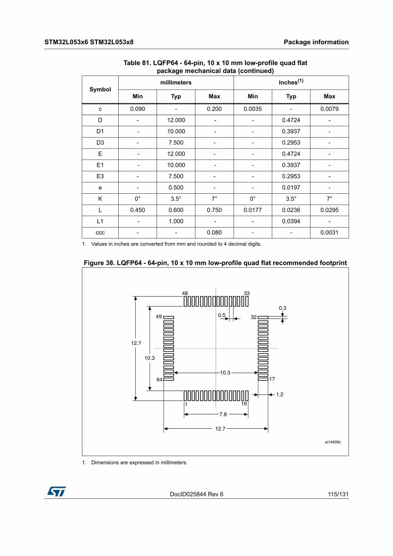
DocID025844 Rev 6 115/131
STM32L053x6 STM32L053x8 Package information
125
Figure 38. LQFP64 - 64-pin, 10 x 10 mm low-profile quad flat recommended footprint
1. Dimensions are expressed in millimeters.
c 0.090 - 0.200 0.0035 - 0.0079
D - 12.000 - - 0.4724 -
D1 - 10.000 - - 0.3937 -
D3 - 7.500 - - 0.2953 -
E - 12.000 - - 0.4724 -
E1 - 10.000 - - 0.3937 -
E3 - 7.500 - - 0.2953 -
e - 0.500 - - 0.0197 -
K 0° 3.5° 7° 0° 3.5° 7°
L 0.450 0.600 0.750 0.0177 0.0236 0.0295
L1 - 1.000 - - 0.0394 -
ccc - - 0.080 - - 0.0031
1. Values in inches are converted from mm and rounded to 4 decimal digits.
Table 81. LQFP64 - 64-pin, 10 x 10 mm low-profile quad flat package mechanical data (continued)
Symbolmillimeters inches(1)
Min Typ Max Min Typ Max

Package information STM32L053x6 STM32L053x8
116/131 DocID025844 Rev 6
Device marking for LQFP64
The following figure gives an example of topside marking versus pin 1 position identifier location.
Figure 39. LQFP64 marking example (package top view)
1. Parts marked as “ES”, “E” or accompanied by an Engineering Sample notification letter, are not yet qualified and therefore not yet ready to be used in production and any consequences deriving from such usage will not be at ST charge. In no event, ST will be liable for any customer usage of these engineering samples in production. ST Quality has to be contacted prior to any decision to use these Engineering samples to run qualification activity.

DocID025844 Rev 6 117/131
STM32L053x6 STM32L053x8 Package information
125
7.2 TFBGA64 package information
Figure 40. TFBGA64 – 64-ball, 5 x 5 mm, 0.5 mm pitch thin profile fine pitch ball grid array package outline
1. Drawing is not to scale.
Table 82. TFBGA64 – 64-ball, 5 x 5 mm, 0.5 mm pitch, thin profile fine pitch ball grid array package mechanical data
Symbolmillimeters inches(1)
Min Typ Max Min Typ Max
A - - 1.200 - - 0.0472
A1 0.150 - - 0.0059 - -
A2 - 0.200 - - 0.0079 -
A4 - - 0.600 - - 0.0236
b 0.250 0.300 0.350 0.0098 0.0118 0.0138
D 4.850 5.000 5.150 0.1909 0.1969 0.2028
D1 - 3.500 - - 0.1378 -
E 4.850 5.000 5.150 0.1909 0.1969 0.2028
E1 - 3.500 - - 0.1378 -

Package information STM32L053x6 STM32L053x8
118/131 DocID025844 Rev 6
Figure 41. TFBGA64 – 64-ball, 5 x 5 mm, 0.5 mm pitch, thin profile fine pitch ball ,grid array recommended footprint
Note: Non solder mask defined (NSMD) pads are recommended.
4 to 6 mils solder paste screen printing process.
e - 0.500 - - 0.0197 -
F - 0.750 - - 0.0295 -
ddd - - 0.080 - - 0.0031
eee - - 0.150 - - 0.0059
fff - - 0.050 - - 0.0020
1. Values in inches are converted from mm and rounded to 4 decimal digits.
Table 83. TFBGA64 recommended PCB design rules (0.5 mm pitch BGA)
Dimension Recommended values
Pitch 0.5
Dpad 0.27 mm
Dsm0.35 mm typ. (depends on the soldermask registration tolerance)
Solder paste 0.27 mm aperture diameter.
Table 82. TFBGA64 – 64-ball, 5 x 5 mm, 0.5 mm pitch, thin profile fine pitch ball grid array package mechanical data (continued)
Symbolmillimeters inches(1)
Min Typ Max Min Typ Max

DocID025844 Rev 6 119/131
STM32L053x6 STM32L053x8 Package information
125
Device marking for TFBGA64
The following figure gives an example of topside marking versus ball A 1 position identifier location.
Figure 42. TFBGA64 marking example (package top view)
1. Parts marked as “ES”, “E” or accompanied by an Engineering Sample notification letter, are not yet qualified and therefore not yet ready to be used in production and any consequences deriving from such usage will not be at ST charge. In no event, ST will be liable for any customer usage of these engineering samples in production. ST Quality has to be contacted prior to any decision to use these Engineering samples to run qualification activity.

Package information STM32L053x6 STM32L053x8
120/131 DocID025844 Rev 6
7.3 LQFP48 package information
Figure 43. LQFP48 - 48-pin, 7 x 7 mm low-profile quad flat package outline
1. Drawing is not to scale.
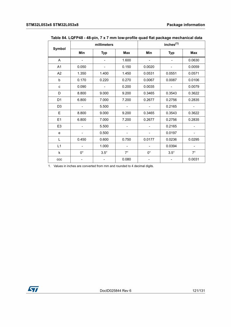
DocID025844 Rev 6 121/131
STM32L053x6 STM32L053x8 Package information
125
Table 84. LQFP48 - 48-pin, 7 x 7 mm low-profile quad flat package mechanical data
Symbolmillimeters inches(1)
1. Values in inches are converted from mm and rounded to 4 decimal digits.
Min Typ Max Min Typ Max
A - - 1.600 - - 0.0630
A1 0.050 - 0.150 0.0020 - 0.0059
A2 1.350 1.400 1.450 0.0531 0.0551 0.0571
b 0.170 0.220 0.270 0.0067 0.0087 0.0106
c 0.090 - 0.200 0.0035 - 0.0079
D 8.800 9.000 9.200 0.3465 0.3543 0.3622
D1 6.800 7.000 7.200 0.2677 0.2756 0.2835
D3 - 5.500 - - 0.2165 -
E 8.800 9.000 9.200 0.3465 0.3543 0.3622
E1 6.800 7.000 7.200 0.2677 0.2756 0.2835
E3 - 5.500 - - 0.2165 -
e - 0.500 - - 0.0197 -
L 0.450 0.600 0.750 0.0177 0.0236 0.0295
L1 - 1.000 - - 0.0394 -
k 0° 3.5° 7° 0° 3.5° 7°
ccc - - 0.080 - - 0.0031

Package information STM32L053x6 STM32L053x8
122/131 DocID025844 Rev 6
Figure 44. LQFP48 - 48-pin, 7 x 7 mm low-profile quad flat recommended footprint
1. Dimensions are expressed in millimeters.
Device marking for LQFP48
The following figure gives an example of topside marking versus pin 1 position identifier location.
Figure 45. LQFP48 marking example (package top view)
1. Parts marked as “ES”, “E” or accompanied by an Engineering Sample notification letter, are not yet qualified and therefore not yet ready to be used in production and any consequences deriving from such usage will not be at ST charge. In no event, ST will be liable for any customer usage of these engineering samples in production. ST Quality has to be contacted prior to any decision to use these Engineering samples to run qualification activity.

DocID025844 Rev 6 123/131
STM32L053x6 STM32L053x8 Package information
125
7.4 Thermal characteristics
The maximum chip-junction temperature, TJ max, in degrees Celsius, may be calculated using the following equation:
TJ max = TA max + (PD max × JA)
Where:
TA max is the maximum ambient temperature in C,
JA is the package junction-to-ambient thermal resistance, in C/W,
PD max is the sum of PINT max and PI/O max (PD max = PINT max + PI/Omax),
PINT max is the product of IDD and VDD, expressed in Watts. This is the maximum chip internal power.
PI/O max represents the maximum power dissipation on output pins where:
PI/O max = (VOL × IOL) + ((VDD – VOH) × IOH),
taking into account the actual VOL / IOL and VOH / IOH of the I/Os at low and high level in the application.
Figure 46. Thermal resistance
Table 85. Thermal characteristics
Symbol Parameter Value Unit
JA
Thermal resistance junction-ambientTFBGA64 - 5 x 5 mm / 0.5 mm pitch
61
°C/WThermal resistance junction-ambientLQFP64 - 10 x 10 mm / 0.5 mm pitch
45
Thermal resistance junction-ambientLQFP48 - 7 x 7 mm / 0.5 mm pitch
55

Package information STM32L053x6 STM32L053x8
124/131 DocID025844 Rev 6
7.4.1 Reference document
JESD51-2 Integrated Circuits Thermal Test Method Environment Conditions - Natural Convection (Still Air). Available from www.jedec.org.

DocID025844 Rev 6 125/131
STM32L053x6 STM32L053x8 Part numbering
125
8 Part numbering
For a list of available options (speed, package, etc.) or for further information on any aspect of this device, please contact your nearest ST sales office.
Table 86. STM32L053x6/8 ordering information scheme
Example: STM32 L 053 R 8 T 6 D TR
Device family
STM32 = ARM-based 32-bit microcontroller
Product type
L = Low power
Device subfamily
053 = USB + LCD
Pin count
C = 48/49 pins
R = 64 pins
Flash memory size
6 = 32 Kbytes
8 = 64 Kbytes
Package
T = LQFP
H = TFBGA
Temperature range
6 = Industrial temperature range, –40 to 85 °C
7 = Industrial temperature range, –40 to 105 °C
3 = Industrial temperature range, –40 to 125 °C
Options
No character = VDD range: 1.8 to 3.6 V and BOR enabled
D = VDD range: 1.65 to 3.6 V and BOR disabled
Packing
TR = tape and reel
No character = tray or tube

Revision history STM32L053x6 STM32L053x8
126/131 DocID025844 Rev 6
9 Revision history
Table 87. Document revision history
Date Revision Changes
07-Feb-2014 1 Initial release.
29-Apr-2014 2
Updated Table 4: Functionalities depending on the working mode (from Run/active down to standby). Added Section 3.2: Interconnect matrix.
Updated Figure 4: STM32L053x6/8 TFBGA64 ballout - 5x 5 mm. Added VREF_OUT additional function to PB0 and PB1, replaced TTa I/O structure by TC, and updated PA0/4/5 and PC5/14 I/O structure, and added note 2. in Table 15: STM32L053x6/8 pin definitions.
Updated Table 24: General operating conditions, Table 21: Voltage characteristics and Table 22: Current characteristics.
Modified conditions in Table 27: Embedded internal reference voltage.
Updated Table 28: Current consumption in Run mode, code with data processing running from Flash, Table 30: Current consumption in Run mode, code with data processing running from RAM, Table 32: Current consumption in Sleep mode, Table 33: Current consumption in Low-power run mode, Table 34: Current consumption in Low-power sleep mode,Table 35: Typical and maximum current consumptions in Stop mode and Table 36: Typical and maximum current consumptions in Standby mode. Added Figure 12: IDD vs VDD, at TA= 25/55/85/105 °C, Run mode, code running from Flash memory, Range 2, HSE, 1WS, Figure 13: IDD vs VDD, at TA= 25/55/85/105 °C, Run mode, code running from Flash memory, Range 2, HSI16, 1WS, Figure 14: IDD vs VDD, at TA= 25/55/ 85/105/125 °C, Low-power run mode, code running from RAM, Range 3, MSI (Range 0) at 64 KHz, 0 WS, Figure 15: IDD vs VDD, at TA= 25/55/ 85/105/125 °C, Stop mode with RTC enabled and running on LSE Low drive and Figure 16: IDD vs VDD, at TA= 25/55/85/105/125 °C, Stop mode with RTC disabled, all clocks off.
Updated Table 43: HSE oscillator characteristics and Table 44: LSE oscillator characteristics. Added Figure 21: HSI16 minimum and maximum value versus temperature.
Updated Table 55: ESD absolute maximum ratings, Table 57: I/O current injection susceptibility, Table 58: I/O static characteristics.
Added Figure 22: VIH/VIL versus VDD (CMOS I/Os) and Figure 23: VIH/VIL versus VDD (TTL I/Os).
Updated Table 59: Output voltage characteristics, Table 60: I/O AC characteristics and Figure 24: I/O AC characteristics definition.
Updated Table 62: ADC characteristics, Table 64: ADC accuracy, and Figure 27: Typical connection diagram using the ADC. Updated Table 67: Temperature sensor characteristics.
Updated Table 73: SPI characteristics in voltage Range 1 and Table 76: I2S characteristics.
Added Figure 46: Thermal resistance.

DocID025844 Rev 6 127/131
STM32L053x6 STM32L053x8 Revision history
130
25-Jun-2014 3
ADC now guaranteed down to 1.65 V.
Cover page: updated core speed, added minimum supply voltage for ADC, DAC and comparators.
Updated list of applications in Section 1: Introduction. Changed number of I2S interfaces to one in Section 2: Description.
Updated RTC/TIM21 in Table 5: STM32L0xx peripherals interconnect matrix.
Updated Table 2: Functionalities depending on the operating power supply range.
Updated Section 3.4.1: Power supply schemes.
Updated Figure 4: STM32L053x6/8 TFBGA64 ballout - 5x 5 mm.
Updated VDDA in Table 24: General operating conditions.
Splitted Table Current consumption in Run mode, code with data processing running from Flash into Table 28 and Table 29 and content updated. Splitted Table Current consumption in Run mode, code with data processing running from RAM into Table 30 and Table 31 and content updated. Updated Table 32: Current consumption in Sleep mode, Table 33: Current consumption in Low-power run mode, Table 34: Current consumption in Low-power sleep mode, Table 35: Typical and maximum current consumptions in Stop mode, Table 36: Typical and maximum current consumptions in Standby mode, and added Table 37: Average current consumption during Wakeup.
Updated Table 38: Peripheral current consumption in Run or Sleep mode and added Table 39: Peripheral current consumption in Stop and Standby mode.
Updated Table 46: HSI48 oscillator characteristics. Removed note 1 below Figure 19: HSE oscillator circuit diagram.
Updated tLOCK in Table 49: PLL characteristics.
Updated Table 51: Flash memory and data EEPROM characteristics and Table 52: Flash memory and data EEPROM endurance and retention.
Updated Table 60: I/O AC characteristics.
Updated Table 62: ADC characteristics.
Updated Figure 46: Thermal resistance and added note 1.
Table 87. Document revision history (continued)
Date Revision Changes

Revision history STM32L053x6 STM32L053x8
128/131 DocID025844 Rev 6
05-Sep-2014 4
Extended operating temperature range to 125 °C.
Updated minimum ADC operating voltage to 1.65 V.
Replaced USART3 by LPUART1 in Table 15: STM32L053x6/8 pin definitions and LPUART by LPUART1 in Table 16: Alternate function port A, Table 17: Alternate function port B, Table 18: Alternate function port C, Table 19: Alternate function port D and Table 20: Alternate function port H. Updated PA6 in Table 16: Alternate function port A.
Updated temperature range in Section 2: Description, Table 1: Ultra-low-power STM32L053x6/x8 device features and peripheral counts.
Updated PD, TA and TJ to add range 3 in Table 24: General operating conditions. Added range 3 in Table 52: Flash memory and data EEPROM endurance and retention, Table 86: STM32L053x6/8 ordering information scheme. Update note 1 in Table 28: Current consumption in Run mode, code with data processing running from Flash, Table 30: Current consumption in Run mode, code with data processing running from RAM, Table 32: Current consumption in Sleep mode, Table 33: Current consumption in Low-power run mode, Table 34: Current consumption in Low-power sleep mode, Table 35: Typical and maximum current consumptions in Stop mode, Table 36: Typical and maximum current consumptions in Standby mode and Table 40: Low-power mode wakeup timings. Updated Figure 46: Thermal resistance and removed note 1. Updated Figure 14: IDD vs VDD, at TA= 25/55/ 85/105/125 °C, Low-power run mode, code running from RAM, Range 3, MSI (Range 0) at 64 KHz, 0 WS, Figure 15: IDD vs VDD, at TA= 25/55/ 85/105/125 °C, Stop mode with RTC enabled and running on LSE Low drive, Figure 16: IDD vs VDD, at TA= 25/55/85/105/125 °C, Stop mode with RTC disabled, all clocks off.
Updated Table 36: Typical and maximum current consumptions in Standby mode.
Updated SYSCFG in Table 38: Peripheral current consumption in Run or Sleep mode.
Updated Table 39: Peripheral current consumption in Stop and Standby mode and Table 40: Low-power mode wakeup timings.
Updated ACCHSI16 temperature conditions in Table 45: 16 MHz HSI16 oscillator characteristics. Changed ambient temperature range in note 1 below Table 46: HSI48 oscillator characteristics.
Updated VF(NRST) and VNF(NRST) in Table 61: NRST pin characteristics.
Updated Table 62: ADC characteristics and Table 64: ADC accuracy.
Added range 3 in Table 86: STM32L053x6/8 ordering information scheme.
Table 87. Document revision history (continued)
Date Revision Changes

DocID025844 Rev 6 129/131
STM32L053x6 STM32L053x8 Revision history
130
08-Sep-2015 5
Updated all pinout/ballout schematics to highlight pin/ball supplied through VDD_USB.
Updated current consumption in Run mode in Section : Features.
Renamed BOOT1 into nBOOT1.
Changed USARTx_RTS into USARTx_RTS_DE and LPUARTx_RTS into LPUARTx_RTS_DE.
Updated VLCD in Section 3.12: Analog-to-digital converter (ADC)
ADC no more available in Low-power run and Low-power Sleep modes in Table 4: Functionalities depending on the working mode (from Run/active down to standby).
Updated Figure 5: STM32L053x6/8 LQFP48 pinout - 7 x 7 mm, Figure 3: STM32L053x6/8 LQFP64 pinout - 10 x 10 mm and Figure 4: STM32L053x6/8 TFBGA64 ballout - 5x 5 mm. Changed I/O structure for PC5 and modified E5 and E6 signals for TFBGA64 in Table 15: STM32L053x6/8 pin definitions.
Added ΣIVDD_USB and updated ΣIIO(PIN) in Table 22: Current characteristics
Updated VDD_USB in Table 24: General operating conditions.
Changed temperature condition in Table 7: Internal voltage reference measured values and Table 26: Embedded internal reference voltage calibration values.
Updated TCoeff in Table 27: Embedded internal reference voltage.
Added note related to Standby mode in Table 39: Peripheral current consumption in Stop and Standby mode.
Updated Figure 14: IDD vs VDD, at TA= 25/55/ 85/105/125 °C, Low-power run mode, code running from RAM, Range 3, MSI (Range 0) at 64 KHz, 0 WS, Figure 15: IDD vs VDD, at TA= 25/55/ 85/105/125 °C, Stop mode with RTC enabled and running on LSE Low drive and Figure 16: IDD vs VDD, at TA= 25/55/85/105/125 °C, Stop mode with RTC disabled, all clocks off.
Updated Table 40: Low-power mode wakeup timings.
Updated MSI oscillator temperature frequency drift in Table 48: MSI oscillator characteristics.
Updated Table 53: EMS characteristics, Table 54: EMI characteristics and Table 55: ESD absolute maximum ratings.
Added tUP_LDO in Table 62: ADC characteristics.
Updated Table 57: I/O current injection susceptibility, Table 58: I/O static characteristics (Ilkg) and Table 60: I/O AC characteristics.
Section : I2C interface characteristics: updated introduction and Table 71: I2C analog filter characteristics.
Updated Figure 31: SPI timing diagram - slave mode and CPHA = 0.
Added Section : Device marking for LQFP64, updated Figure 42: TFBGA64 marking example (package top view) and Figure 45: LQFP48 marking example (package top view) as well as notes below schematics.
Table 87. Document revision history (continued)
Date Revision Changes
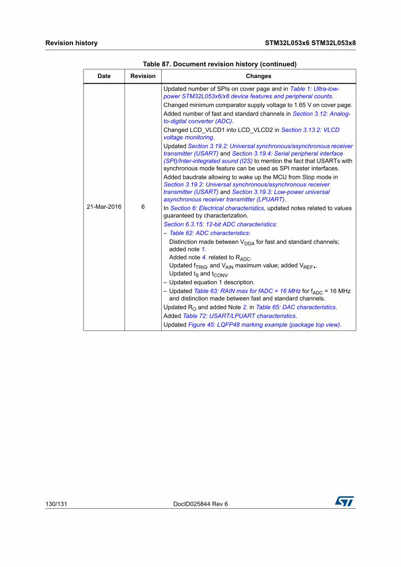
Revision history STM32L053x6 STM32L053x8
130/131 DocID025844 Rev 6
21-Mar-2016 6
Updated number of SPIs on cover page and in Table 1: Ultra-low-power STM32L053x6/x8 device features and peripheral counts.
Changed minimum comparator supply voltage to 1.65 V on cover page.
Added number of fast and standard channels in Section 3.12: Analog-to-digital converter (ADC).
Changed LCD_VLCD1 into LCD_VLCD2 in Section 3.13.2: VLCD voltage monitoring.
Updated Section 3.19.2: Universal synchronous/asynchronous receiver transmitter (USART) and Section 3.19.4: Serial peripheral interface (SPI)/Inter-integrated sound (I2S) to mention the fact that USARTs with synchronous mode feature can be used as SPI master interfaces.
Added baudrate allowing to wake up the MCU from Stop mode in Section 3.19.2: Universal synchronous/asynchronous receiver transmitter (USART) and Section 3.19.3: Low-power universal asynchronous receiver transmitter (LPUART).
In Section 6: Electrical characteristics, updated notes related to values guaranteed by characterization.
Section 6.3.15: 12-bit ADC characteristics:
– Table 62: ADC characteristics:
Distinction made between VDDA for fast and standard channels; added note 1.Added note 4. related to RADC.Updated fTRIG. and VAIN maximum value; added VREF+.Updated tS and tCONV.
– Updated equation 1 description.
– Updated Table 63: RAIN max for fADC = 16 MHz for fADC = 16 MHz and distinction made between fast and standard channels.
Updated RO and added Note 2. in Table 65: DAC characteristics.
Added Table 72: USART/LPUART characteristics.
Updated Figure 45: LQFP48 marking example (package top view).
Table 87. Document revision history (continued)
Date Revision Changes
DocID025844 Rev 6 131/131
STM32L053x6 STM32L053x8
131
IMPORTANT NOTICE – PLEASE READ CAREFULLY
STMicroelectronics NV and its subsidiaries (“ST”) reserve the right to make changes, corrections, enhancements, modifications, and improvements to ST products and/or to this document at any time without notice. Purchasers should obtain the latest relevant information on ST products before placing orders. ST products are sold pursuant to ST’s terms and conditions of sale in place at the time of order acknowledgement.
Purchasers are solely responsible for the choice, selection, and use of ST products and ST assumes no liability for application assistance or the design of Purchasers’ products.
No license, express or implied, to any intellectual property right is granted by ST herein.
Resale of ST products with provisions different from the information set forth herein shall void any warranty granted by ST for such product.
ST and the ST logo are trademarks of ST. All other product or service names are the property of their respective owners.
Information in this document supersedes and replaces information previously supplied in any prior versions of this document.
© 2016 STMicroelectronics – All rights reserved