Ultra-fast perpendicular Spin Orbit Torque MRAM
15
1 Ultra-fast perpendicular Spin Orbit Torque MRAM Murat Cubukcu*, 1 , Olivier Boulle 1, † , Nikolaï Mikuszeit 1 , Claire Hamelin 1 , Thomas Brächer 1 , Nathalie Lamard 6 , Marie-Claire Cyrille 6 , Liliana Buda-Prejbeanu 1 , Kevin Garello 2 , Ioan Mihai Miron 1 , O. Klein 1 , G. de Loubens 4 , V. V. Naletov 1,4,5 , Juergen Langer 3 , Berthold Ocker 3 , Pietro Gambardella 2 and Gilles Gaudin 1 1 Univ. Grenoble Alpes, CEA, CNRS, Grenoble INP, INAC, SPINTEC, F-38000 Grenoble, France 2 Department of Materials, ETH Zurich, Hönggerbergring 64, CH-8093 Zürich, Switzerland 3 Singulus Technologies, Hanauer Landstr, 103, 63796, Kahl am Main, Germany 4 Service de Physique de l’Etat Condensé (CNRS URA 2464), CEA Saclay, 91191 Gif-sur-Yvette, France 5 Institute of Physics, Kazan Federal University, Kazan 420008, Russian Federation 6 CEA Leti, F-38000 , Grenoble, France We demonstrate ultra-fast (down to 400 ps) bipolar magnetization switching of a three- terminal perpendicular Ta/FeCoB/MgO/FeCoB magnetic tunnel junction. The critical current density rises significantly as the current pulse shortens below 10 ns, which translates into a minimum in the write energy in the ns range. Our results show that SOT-MRAM allows fast brought to you by CORE View metadata, citation and similar papers at core.ac.uk provided by UCL Discovery
Transcript of Ultra-fast perpendicular Spin Orbit Torque MRAM
1
Ultra-fast perpendicular Spin Orbit Torque MRAM
Murat Cubukcu*,1, Olivier Boulle1, † , Nikolaï Mikuszeit1, Claire Hamelin1, Thomas Brächer1,
Nathalie Lamard6, Marie-Claire Cyrille6 , Liliana Buda-Prejbeanu1, Kevin Garello2, Ioan
Mihai Miron1, O. Klein1, G. de Loubens4, V. V. Naletov1,4,5, Juergen Langer3, Berthold
Ocker3, Pietro Gambardella2 and Gilles Gaudin1
1 Univ. Grenoble Alpes, CEA, CNRS, Grenoble INP, INAC, SPINTEC, F-38000 Grenoble, France 2 Department of Materials, ETH Zurich, Hönggerbergring 64, CH-8093 Zürich, Switzerland
3 Singulus Technologies, Hanauer Landstr, 103, 63796, Kahl am Main, Germany
4 Service de Physique de l’Etat Condensé (CNRS URA 2464), CEA Saclay, 91191 Gif-sur-Yvette,
France
5 Institute of Physics, Kazan Federal University, Kazan 420008, Russian Federation
6 CEA Leti, F-38000 , Grenoble, France
We demonstrate ultra-fast (down to 400 ps) bipolar magnetization switching of a three-
terminal perpendicular Ta/FeCoB/MgO/FeCoB magnetic tunnel junction. The critical current
density rises significantly as the current pulse shortens below 10 ns, which translates into a
minimum in the write energy in the ns range. Our results show that SOT-MRAM allows fast
brought to you by COREView metadata, citation and similar papers at core.ac.uk
provided by UCL Discovery

2
and low power write operations, which renders it promising for non-volatile cache memory
applications.
3
The introduction of non-volatility at the cache level is a major challenge to the IT industry as
it would lead to a large decrease of the power consumption of microprocessors by minimizing
their static and dynamic power consumption and pave the way towards normally-off/instant-
on computing. Among other technologies, STT-MRAM has been identified as a promising
candidate for the non-volatile replacement of SRAM cache memory technology[1]. STT-MRAM
combines CMOS compatibility, high retention time (10 years), large endurance and relatively
fast write time (down to 4 ns for reliable switching in perpendicular STT-MRAM[2]). However,
cache memory applications typically require faster operations (ns for L1 cache) combined
with a large endurance due to their high access rate. Very fast switching (sub-ns) has been
recently demonstrated using stacks where the magnetizations of the free and the fixed layers
are perpendicular[3]–[5]. However, this gain in operation speed comes at the expense of a
rise in the current flowing through the tunnel barrier. As a consequence, manufacturers are
currently facing reliability issues due to the accelerated aging of the tunnel barrier when
injecting these high write current densities[6], [7]. Another drawback of STT-MRAM is that
reading and writing use the same current path. This results in an undesired writing during the
read-out of the bit[7] as well as a high read power since the tunnel barrier needs to have a
very small resistance to sustain the large writing current densities.
Recently, we have proposed a novel memory concept, named Spin-Orbit Torque-MRAM (SOT-
MRAM), that combines the STT advantages and naturally solves the above mentioned
issues[8]–[10]. The memory is based on the discovery that a current flowing in the plane of a
magnetic multilayer with structural inversion asymmetry, such as Pt/Co/AlOx, exerts a torque
on the magnetization, which can lead to magnetization reversal[9], [11], [12]. Such a torque
4
arises from the conversion of the orbital to spin angular momentum through the spin Hall
effect in the heavy metal and/or the Rashba-Edelstein effect at the interfaces[9], [13]–[15].
The key advantage of the SOT-MRAM is that writing and reading are decoupled due to their
independent current paths. Thus, the SOT-MRAM intrinsically solves the reliability issues in
current STT-MRAM promising a potentially unlimited endurance.
To be a strong candidate for non-volatile cache memory applications, SOT-MRAM needs to be
fast. We recently demonstrated deterministic switching induced by current pulses shorter
than 200 ps in dots made of Pt/Co/AlOx stacks[12]. However, the use of a Pt seed layer in MgO
based MTJ does not allow to reach the high TMR ratio needed for memory applications[16],
[17] (>100%), as it promotes a (111) fcc texture while a (100) bcc structure at the CoFe/MgO
interface is needed to achieve high TMR [18]–[20]On the contrary, the Ta/FeCoB/MgO/FeCoB
MTJ stacks commonly used for STT-MRAM seem ideal for SOT-MRAM since they combine a
high TMR, a perpendicular magnetization[21] and a large spin Hall effect in Ta[22]. In this
article, we demonstrate that magnetization switching can be achieved by very short current
pulses (down to 400 ps) in Ta/FeCoB/MgO three-terminal SOT-MRAM memory cells. Our
results show that SOT-MRAM allows for fast, and low-power write operations, rendering it
promising for non-volatile cache memory applications.
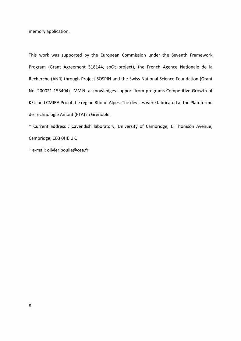
The magnetic tunnel junctions (MTJ) was deposited by magnetron sputtering using a Singulus
Timaris® deposition machine with the following structure[23]–[25] 10 Ta/1 Fe60Co20B20/MgO/
1.3 Fe60Co20B20/0.3 Ta/FM1/Ru0.85/FM2 (thicknesses in nm), where FM1=[0.4 Co/ 0.4 Cu/ 1.4
Pt]x5 /0.6 Co and FM2=0.6 Co/[0.4 Cu/ 1.4 Pt/ 0.4 Co]x12/ 0.4 Cu/2 Pt (see Fig. 1(a)). Functional
three-terminal single cells with lateral dimensions down to 150 nm diameter on top of a 330

5
nm wide Ta track were fabricated as described in Ref.[26] The results presented here are
obtained from a sample with a 275 nm diameter MTJ on top of a 635 nm Ta track (see Fig.1
(b)). All measurement are carried out at room temperature. Figure 1 (c) shows a typical TMR
hysteresis cycle corresponding to the successive reversal of the FeCoB (1 nm) free layer and
pinned layer, the magnetic field being applied perpendicularly to the sample plane. A TMR of
up to 55%, associated with a sharp reversal of the magnetization of the free layer, is observed.
The resistance area product of the junction is about 600 .µm². For the current induced
magnetization switching experiments, current pulses are injected in the Ta bottom track using
a fast voltage pulse generator whereas the TMR signal is measured using a DC voltage source
connected to the MTJ in series with a 1M resistor. This resistor prevents high voltages spikes
on the MTJ during the pulse injection. A 100 resistor was connected in parallel to the track
to minimize the impedance mismatch. The pulse rise time is 220 ps for pulse widths P <2 ns,
and 1.5 ns for wider pulses. The pulse width is defined as the full width at half maximum.
Figure 2 (a) shows the TMR signal measured after the pulse injection as a function of the
amplitude of the current pulse injected in the track. An in-plane magnetic field µ0Hip=100 mT
is applied along the current direction to allow for the bipolar switching[9]. The current pulse
is 550 ps long. Starting from the low resistance state and increasing the current, a sharp
increase in the TMR signal is observed above a positive threshold pulse amplitude,
demonstrating the reversal of the magnetization of the FeCoB bottom free layer from the
parallel (P) to the anti-parallel (AP) configurations of the magnetizations. From the AP
configuration, a large enough negative current allows to go back to the P configuration. This
demonstrates the writing of a perpendicular SOT-MRAM memory cell by a 550 ps current
pulse and its reading by the TMR signal. Note that the switching current for the P to AP

6
switching is slightly lower than the one for the AP to P, which can be explained by the dipolar
interaction between the bottom free layer and the not fully compensated synthetic
antiferromagnet. The corresponding switching-current density is about 3.3x10¹² A/m². The
switching probability from the P to the AP configuration as a function of the amplitude of the
current for different pulse widths is plotted in Fig. 2(b) (each point is an average over 30
events) [27]. Interestingly, recent time-resolved X-ray microscopy imaging of the spin orbit
torque driven magnetization reversal of Pt/Co/AlOx dots revealed that the switching
probability measured electrically is not the probability of an on/off event, but more likely the
fraction of the magnetic layer area that has switched[28]. The same measurements show that
there are no ringing or after – pulse effects associated to switching.
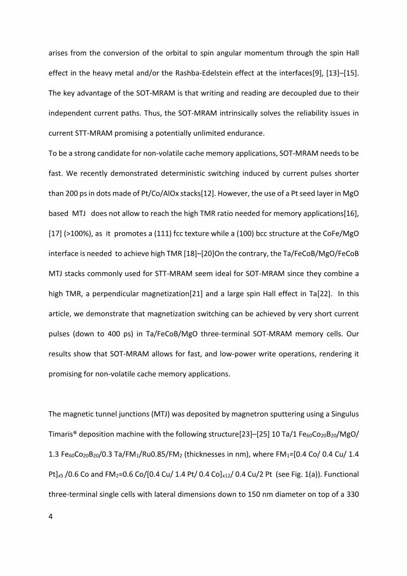
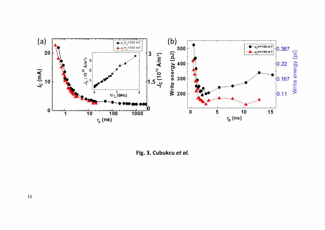
Magnetization switching is observed in the whole range of pulse widths from 400 ps to 2.5 µs
and is bipolar: positive currents lead to a magnetization switching from P to AP, whereas
negative currents lead to a switching from AP to P. The switching current Ic strongly depends
on the pulse length P (see Fig. 3(a)). For P>10 ns, Jc changes little with P and scales
approximately linearly on log(P) suggesting a thermally activated regime where stochastic
fluctuations help the magnetization to overcome the reversal energy barrier [29], [30]. For P<
10 ns, a large increase of Jc is observed as P decreases and Jc scales linearly on 1/P (see Fig.3(a)
inset). For P< 10 ns, a large increase of Jc is observed as P decreases and Jc scales linearly on
1/P (see Fig.3(a) inset). This scaling is reminiscent of early spin transfer torque predictions [31]
and experiments [32] where the injected spin current polarization is aligned along the uniaxial
anisotropy axis. Such a scaling is expected from the conservation of spin angular momentum,
assuming the magnetization is spatially homogeneous (macrospin approximation). A different
scaling is however expected in our spin orbit torque geometry where the current spin
7
polarization is aligned perpendicular to the uniaxial anisotropy axis [12], [33]. On the other
hand, several experimental study have shown that for lateral sizes typically larger than 50 nm,
the magnetization reversal by spin transfer and spin orbit torques occurs by domain
nucleation followed by domain wall propagation[28], [34]–[41]. In such a case, a 1/P scaling of
the critical current is expected, which expresses that the switching time is the time for a
nucleated domain wall to travel across the dot.
As expected, the switching current depends also on the external in-plane magnetic field Hip
and decreases as Hip increases (Fig. 3(a)). The corresponding write energy E=RI²P is plotted in
Fig. 3(b) as function of P, assuming it is dissipated in a 3 kΩ resistance standing for the Ta
track and the addressing transistor. The energy depends non-monotonously on P with a large
increase of the energy as P decreases for P<1 ns. Interestingly, a minimum in the write energy
is observed between 1 and 3 ns. This feature is explained by the crossover between the
thermally activated regime for large pulse width and the short pulse width regime. The energy
scale extrapolated for a 50 nm wide and 3 nm thick Ta track is shown in blue on the right
vertical axis A write energy of about 95 fJ at 1.5 ns can be reached, associated with a write
current of about 180 µA, which is similar to the best results obtained so far for current
perpendicular STT-MRAM technology[42], [43].
In conclusion, we demonstrate ultra-fast (down to 400 ps) bipolar and deterministic writing of
perpendicular three-terminal spin-orbit torque (SOT)-MRAM single cells with a
Ta/CoFeB/MgO/CoFeB MTJ structure. The switching current density rises significantly as the
pulse shortens below 10 ns. This translates into a write energy minimum in the ns range.
These experimental results extrapolate to a switching current of around 180 µA at 1.5 ns for
50 nm track width. This makes SOT-MRAM promising for a power efficient non-volatile cache
8
memory application.
This work was supported by the European Commission under the Seventh Framework
Program (Grant Agreement 318144, spOt project), the French Agence Nationale de la
Recherche (ANR) through Project SOSPIN and the Swiss National Science Foundation (Grant
No. 200021-153404). V.V.N. acknowledges support from programs Competitive Growth of
KFU and CMIRA'Pro of the region Rhone-Alpes. The devices were fabricated at the Plateforme
de Technologie Amont (PTA) in Grenoble.
* Current address : Cavendish laboratory, University of Cambridge, JJ Thomson Avenue,
Cambridge, CB3 0HE UK,
† e-mail: [email protected]
9
References
[1] The International Technology Roadmap for Semiconductors, “http://www.itrs.net/Links/2013ITRS/2013Chapters/2013ERD.pdf.”
[2] G. Jan et al., “Demonstration of fully functional 8Mb perpendicular STT-MRAM chips with sub-5ns writing for non-volatile embedded memories,” in 2014 Symposium on VLSI Technology (VLSI-Technology): Digest of Technical Papers, 2014, pp. 1–2.
[3] H. Liu, D. Bedau, D. Backes, J. A. Katine, J. Langer, and A. D. Kent, “Ultrafast switching in magnetic tunnel junction based orthogonal spin transfer devices,” Appl. Phys. Lett., vol. 97, no. 24, p. 242510, 2010.
[4] M. M. de Castro et al., “Precessional spin-transfer switching in a magnetic tunnel junction with a synthetic antiferromagnetic perpendicular polarizer,” J. Appl. Phys., vol. 111, no. 7, p. 07C912, Apr. 2012.
[5] G. E. Rowlands et al., “Deep subnanosecond spin torque switching in magnetic tunnel junctions with combined in-plane and perpendicular polarizers,” Appl. Phys. Lett., vol. 98, no. 10, p. 102509, Mar. 2011.
[6] G. Panagopoulos, C. Augustine, and K. Roy, “Modeling of dielectric breakdown-induced time-dependent STT-MRAM performance degradation,” in Device Research Conference (DRC), 2011 69th Annual, 2011, pp. 125–126.
[7] W. S. Zhao et al., “Failure and reliability analysis of STT-MRAM,” Microelectron. Reliab., vol. 52, no. 9–10, pp. 1848–1852, Sep. 2012.
[8] G. Gaudin, I. M. Miron, P. Gambardella, and A. Schuhl, “A writable magnetic memory element,” 12/899,072; 12/899,091; 12/959,980.
[9] I. M. Miron et al., “Perpendicular switching of a single ferromagnetic layer induced by in-plane current injection,” Nature, vol. 476, no. 7359, pp. 189–193, 2011.
[10] G. Prenat, K. Jabeur, G. D. Pendina, O. Boulle, and G. Gaudin, “Beyond STT-MRAM, Spin Orbit Torque RAM SOT-MRAM for High Speed and High Reliability Applications,” in Spintronics-based Computing, W. Zhao and G. Prenat, Eds. Springer International Publishing, 2015, pp. 145–157.
[11] C. Onur Avci et al., “Magnetization switching of an MgO/Co/Pt layer by in-plane current injection,” Appl. Phys. Lett., vol. 100, no. 21, p. 212404, May 2012.
[12] K. Garello et al., “Ultrafast magnetization switching by spin-orbit torques,” Appl. Phys. Lett., vol. 105, no. 21, p. 212402, Nov. 2014.
[13] L. Liu, C.-F. Pai, Y. Li, H. W. Tseng, D. C. Ralph, and R. A. Buhrman, “Spin-Torque Switching with the Giant Spin Hall Effect of Tantalum,” Science, vol. 336, no. 6081, pp. 555–558, May 2012.
[14] K. Garello et al., “Symmetry and magnitude of spin-orbit torques in ferromagnetic heterostructures,” Nat. Nanotechnol., vol. 8, no. 8, pp. 587–593, Aug. 2013.
[15] J. Kim et al., “Layer thickness dependence of the current-induced effective field vector in Ta|CoFeB|MgO,” Nat. Mater., 2012.
[16] Y. J. Song et al., “Highly functional and reliable 8Mb STT-MRAM embedded in 28nm logic,” in 2016 IEEE International Electron Devices Meeting (IEDM), 2016, p. 27.2.1-27.2.4.

10
[17] J. J. Kan et al., “Systematic validation of 2x nm diameter perpendicular MTJ arrays and MgO barrier for sub-10 nm embedded STT-MRAM with practically unlimited endurance,” in 2016 IEEE International Electron Devices Meeting (IEDM), 2016, p. 27.4.1-27.4.4.
[18] S. S. P. Parkin et al., “Giant tunnelling magnetoresistance at room temperature with MgO (100) tunnel barriers,” Nat. Mater., vol. 3, no. 12, pp. 862–867, Dec. 2004.
[19] W. H. Butler, X.-G. Zhang, T. C. Schulthess, and J. M. MacLaren, “Spin-dependent tunneling conductance of $\mathrmFe|\mathrmMgO|\mathrmFe$ sandwiches,” Phys. Rev. B, vol. 63, no. 5, p. 054416, Jan. 2001.
[20] S. Yuasa, T. Nagahama, A. Fukushima, Y. Suzuki, and K. Ando, “Giant room-temperature magnetoresistance in single-crystal Fe/MgO/Fe magnetic tunnel junctions,” Nat. Mater., vol. 3, no. 12, pp. 868–871, Dec. 2004.
[21] S. Ikeda et al., “A perpendicular-anisotropy CoFeB–MgO magnetic tunnel junction,” Nat. Mater., vol. 9, no. 9, pp. 721–724, Sep. 2010.
[22] L. Liu, C.-F. Pai, Y. Li, H. W. Tseng, D. C. Ralph, and R. A. Buhrman, “Spin-Torque Switching with the Giant Spin Hall Effect of Tantalum,” Science, vol. 336, no. 6081, pp. 555–558, May 2012.
[23] D. C. Worledge et al., “Spin torque switching of perpendicular Ta∣CoFeB∣MgO-based magnetic tunnel junctions,” Appl. Phys. Lett., vol. 98, no. 2, p. 022501, 2011.
[24] L. Cuchet, B. Rodmacq, S. Auffret, R. C. Sousa, C. Ducruet, and B. Dieny, “Influence of a Ta spacer on the magnetic and transport properties of perpendicular magnetic tunnel junctions,” Appl. Phys. Lett., vol. 103, no. 5, p. 052402, 2013.
[25] L. Cuchet, B. Rodmacq, S. Auffret, R. C. Sousa, and B. Dieny, “Influence of magnetic electrodes thicknesses on the transport properties of magnetic tunnel junctions with perpendicular anisotropy,” Appl. Phys. Lett., vol. 105, no. 5, p. 052408, Aug. 2014.
[26] M. Cubukcu et al., “Spin-orbit torque magnetization switching of a three-terminal perpendicular magnetic tunnel junction,” Appl. Phys. Lett., vol. 104, no. 4, p. 042406, Jan. 2014.
[27] “Higher current density/pulse width could not been probed due to the limited life time of the measured samples, which was related to unoptimized nanofabrication process and RF measurement design.”
[28] M. Baumgartner et al., “Spatially and time-resolved magnetization dynamics driven by spin–orbit torques,” Nat. Nanotechnol., vol. advance online publication, Aug. 2017.
[29] K.-S. Lee, S.-W. Lee, B.-C. Min, and K.-J. Lee, “Thermally activated switching of perpendicular magnet by spin-orbit spin torque,” Appl. Phys. Lett., vol. 104, no. 7, p. 072413, Feb. 2014.
[30] E. B. Myers, F. J. Albert, J. C. Sankey, E. Bonet, R. A. Buhrman, and D. C. Ralph, “Thermally Activated Magnetic Reversal Induced by a Spin-Polarized Current,” Phys. Rev. Lett., vol. 89, no. 19, p. 196801, Oct. 2002.
[31] J. Z. Sun, “Spin-current interaction with a monodomain magnetic body: A model study,” Phys. Rev. B, vol. 62, no. 1, pp. 570–578, Jul. 2000.
[32] P. M. Braganca, O. Ozatay, A. G. F. Garcia, O. J. Lee, D. C. Ralph, and R. A. Buhrman, “Enhancement in spin-torque efficiency by nonuniform spin current generated within a tapered nanopillar spin valve,” Phys. Rev. B, vol. 77, no. 14, p. 144423, Apr. 2008.
[33] J. Park, G. E. Rowlands, O. J. Lee, D. C. Ralph, and R. A. Buhrman, “Macrospin modeling of sub-ns pulse switching of perpendicularly magnetized free layer via spin-orbit torques for cryogenic memory applications,” Appl. Phys. Lett., vol. 105, no. 10, p. 102404, Sep.

11
2014. [34] G. Yu et al., “Magnetization switching through spin-Hall-effect-induced chiral domain
wall propagation,” Phys. Rev. B, vol. 89, no. 10, p. 104421, Mar. 2014. [35] M. M. Decker et al., “Time Resolved Measurements of the Switching Trajectory of
$\mathrmPt/\mathrmCo$ Elements Induced by Spin-Orbit Torques,” Phys. Rev. Lett., vol. 118, no. 25, p. 257201, Jun. 2017.
[36] D. P. Bernstein et al., “Nonuniform switching of the perpendicular magnetization in a spin-torque-driven magnetic nanopillar,” Phys. Rev. B, vol. 83, no. 18, p. 180410, mai 2011.
[37] C. Zhang, S. Fukami, H. Sato, F. Matsukura, and H. Ohno, “Spin-orbit torque induced magnetization switching in nano-scale Ta/CoFeB/MgO,” Appl. Phys. Lett., vol. 107, no. 1, p. 012401, Jul. 2015.
[38] H. Sato et al., “Junction size effect on switching current and thermal stability in CoFeB/MgO perpendicular magnetic tunnel junctions,” Appl. Phys. Lett., vol. 99, no. 4, p. 042501, Jul. 2011.
[39] J. Z. Sun et al., “Effect of subvolume excitation and spin-torque efficiency on magnetic switching,” Phys. Rev. B, vol. 84, no. 6, p. 064413, Aug. 2011.
[40] C. J. Durrant, R. J. Hicken, Q. Hao, and G. Xiao, “Scanning Kerr microscopy study of current-induced switching in Ta/CoFeB/MgO films with perpendicular magnetic anisotropy,” Phys. Rev. B, vol. 93, no. 1, p. 014414, Jan. 2016.
[41] O. J. Lee et al., “Central role of domain wall depinning for perpendicular magnetization switching driven by spin torque from the spin Hall effect,” Phys. Rev. B, vol. 89, no. 2, p. 024418, Jan. 2014.
[42] D. Saida et al., “Low-Current High-Speed Spin-Transfer Switching in a Perpendicular Magnetic Tunnel Junction for Cache Memory in Mobile Processors,” IEEE Trans. Magn., vol. 50, no. 11, pp. 1–5, Nov. 2014.
[43] L. Thomas et al., “Perpendicular spin transfer torque magnetic random access memories with high spin torque efficiency and thermal stability for embedded applications (invited),” J. Appl. Phys., vol. 115, no. 17, p. 172615, May 2014.

12
Figure caption
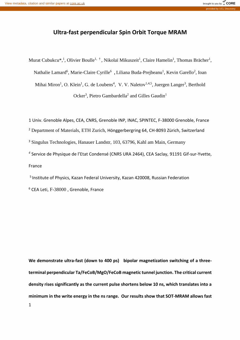
Fig.1 (a) Sketch of the three-terminal MTJ. (b) Scanning electron microscopy image of a 275
nm diameter MTJ on top of a 635 nm wide Ta track. (c) Resistance as a function of the magnetic
field applied perpendicularly to the sample plane.
Fig. 2 (a) TMR as a function of the current pulse amplitude IP (P=0.55 ns long) in the presence
of an external in-plane magnetic field µ0Hip=100 mT. The TMR is measured after the injection
of the current pulse. The arrows show the sweep direction of IP. (b) Switching probability (Psw)
from the P to the AP configuration as a function of IP for three different pulse lengths P=0.55
ns (black, square), P=0.89 ns (red, circles) and P=1 ns (blue, circles) at an applied field
µ0Hip=100 mT.
Fig.3 (a) Switching current Ic as a function of the current pulse length P for two values of the
external in-plane magnetic field (P to AP switching). Inset: Ic vs 1/P for µ0Hip = 100 mT. (b)
Energy dissipated in a 3 k resistor (simulating the resistance of the Ta track and the
transistor) as a function of P for two values of HIP using the write current for the three-
terminal device with a 635 nm wide Ta track. The blue scale on the right shows the write
energy extrapolated for a 50 nm wide and 3 nm thick Ta track.
13
Fig. 1 Cubukcu et al.
(a) (c)
JTa
FeCoB
MgO
FeCoB
FM2
Ru
FM1
Hip-100 0 100
0
20
40
60
TM
R (
%)
H (mT)
MTJ1MΩ
Ta
200 nm
(b)

14
.
Fig. 2. Cubukcu et al
(a) (b)
10 15 20 250
1
P =0.55 ns
P =0.9 ns
P = 1 ns
PS
W
IP (mA)
-40 -20 0 20 40
0
20
40
60
4.5-4.5 0 3
TM
R (
%)
IP (mA)
-3J (10
12A/m2)
15
Fig. 3. Cubukcu et al.
![Test System Requirements For Wafer Level MRAM Test SWTW-2004 Page [1] Test System Requirements For Wafer Level MRAM Test Raphael Robertazzi IBM/Infineon MRAM Development Alliance With](https://static.fdocuments.us/doc/165x107/5acbb8087f8b9a27628ba54b/test-system-requirements-for-wafer-level-mram-swtw-2004-page-1-test-system-requirements.jpg)