UILU-ENG 72-2203 INVESTIGATION OF THE SCATTERING OF …
126
UILU-ENG 72-2203 INVESTIGATION OF THE SCATTERING OF LOW ENERGY ELECTRONS FROM THE SURFACE OF SINGLE CRYSTAL ALUMINUM by James Michael Burkstrand This work was su;ported in part by the Joint Services Electronics Program (U. S, Army, U. S, Navy and U. S. Air Force) under Contract DAAB-07-67-C-0199, in part by the American Chemical Society, Petroleum Research Fund under Contract PRF 3668-A3,5, and in part by the Air Force Office of Scientific Research, Office of Aerospace Research, USAF, under Grant AFOSR-71-2034. Reproduction in whole or in part is permitted for any purpose of the United States Government. This document has been approved for public release and sale; its distribution is unlimited.
Transcript of UILU-ENG 72-2203 INVESTIGATION OF THE SCATTERING OF …
UILU-ENG 72-2203
INVESTIGATION OF THE SCATTERING OF LOW ENERGY ELECTRONS
FROM THE SURFACE OF SINGLE CRYSTAL ALUMINUM
by
James Michael Burkstrand
This work was su;ported in part by the Joint Services Electronics
Program (U. S, Army, U. S, Navy and U. S. Air Force) under Contract
DAAB-07-67-C-0199, in part by the American Chemical Society, Petroleum
Research Fund under Contract PRF 3668-A3,5, and in part by the Air Force
Office of Scientific Research, Office of Aerospace Research, USAF, under
Grant AFOSR-71-2034.
Reproduction in whole or in part is permitted for any purpose
of the United States Government.
This document has been approved for public release and sale;
its distribution is unlimited.

INVESTIGATION OF THE SCATTERING OF LOW ENERGY ELECTRONS
FROM THE SURFACE OF SINGLE CRYSTAL ALUMINUM
James Michael Burkstrand, Ph.D" Department of Physics
lJni\lersity of Illinois at Urbana-Champaign, 1972
Elastic and inelastic low energy electron diffraction (ELEED, ILEED)
observations have been made on a clean surface of Al(lOO). Measurements on the
(10) and (11) elastic diffraction beams were made using normally incident
electrons in the energy range 30 ~ E ~ 170 eV. Peaks in the energy loss
distribution are seen near 5, 10, 15, 26 and 31 eV, the dominant peaks near 10
and 15 eV corresponding to surface and bulk plasmon excitations respectively.
Two types of structure are observed in the inelastic angular profiles: one
closely correlated with the structure in the elastic angular profile, and the
second being substructure corresponding to different ILEED conditions. Energy
intensity profiles (as a function of incident energy) for the (10) and (11)
elastic and inelastic diffraction beams have been measured. These profiles
also show primary and secondary structure. Within the substructure of the
angular and energy intensity profiles are the first experimental observations
of sideband diffraction. A comparison of the experimental results and the
theoretical predictions of Duke and Laramore and of Duke and Bagchi is made.

iii
ACKNOWLEDGEMENTS
The author wishes to thank: his advisor, Professor F. M. Propst,
for his kind encouragement and many contributions to this work; Professor C. B.
Duke, for his explanation of many of the theoretical details of low energy
electron diffraction and for his encouragement and aid in completing this work;
his wife, for her patience and warm support; his parents, for their encouragement
and understanding given for many years; Tom Cooper, for,his friendship and his
designing and constructing the original instrument; Chris Foster, Paul Luscher,
John Wendelken, Steve Withrow, George Laramore, Dave Edwards and Amit Bagchi
for both friendship and scientific contributions; Professor M. Metzger, for
supplying the aluminum crystal and his technical experience in its preparation;
Bob Bales, Bob MacFarlane, Nick Vassos and the rest of the technical staff of
the Coordinated Science Laboratory for their enthusiastic and imaginative
technical assistance in their respective fields.

1.
iv
TABLE OF CONTENTS
Page
INTRQDU CT I QN o e e Cl o e e Ill e i) o e a e o o o o o o e e 111 o 11 o o o If ll o Ill Ill o e o o o • e e o o o o e e Ill • Ill Ill o Ill • 1
1.1 Problem~ 0 e 0 Ill fl 0 Ill .. 0 e. 0 0 0 0. 0 Ill. II •• 0. 0 .. Cl It n 0 e " .... 0 e 0. 0 •• "Ill ••••••••• 1
1.2 Definition of the Measurement~~·~···"•e••••e•o••••o•o••······· 2
Historical Background Ill 0 II •• 0 D ••• Ill • 0 e 0 II • Cl • 0 0 (I • 0 • II •• ., • 1!1 •••••••• II 7 1.3
1.4 Theoretical Discussion ••.•..••......•...•••..••••••••..•..... 12
2. APPARATUS AND EXPERIMENTAL PROCEDURE •••••••••••.••.••.•••.••..•..• 30
2.1
2.2
2.3
2.4
2.5
2.6
2.7
2.8
Introduction. " ••.• " • Ill 0 ... 0 II " •••••••• ., " •• ., •• " • " .. " • • • • • • • • • • • • • • 30
Electron Gun (I 0 II 0 Cl 0 0 (\ 0 ~ 0. (I e e. 0. e 0 0. Ill ••• 0 0 0. II II 0 0 •• Ill •••••••• e ••• 32
Target and Target Assembly. 32
Detector .. 0 0 (I 0 0 0. e. 0 II 0 •• e. e It •• 0. 0 0. 0. 0. e e 0 0 •• (J. II II. 0 II •• It 0 0 •••• II 35
Sputtering Ion
Vacuum System.
Gun. Ill •••• It 0 ••••• e ••• 0 II • II • II • Ill e • 0 • 0 •••• 0 •••••••• 37
38
Electronic Circuitry e. o., eo"'"~~.". c. co e.,. eo o o c l!r ~" "., "o ""' o •• " •• o • .,. 40
Target preparation Ill e G e 0 0 0 0 0 • • • 0 " • 0 0 0 0 I) 0 0 0 e 0 0 • 0 • • • 0 I) tl> 0 0 ct • • .. 0 • e 4 3
2. 9 Criteria for Surface Cleanliness.,........................... 45
2.10 Instrument Checkout ....••..•........••..•................... 49
3. DATA PRESENTATION AND DISCUSSION ••...•••....••.••.•..•••••.•. , .•. , 52
3.1 Measurement of the Absolute Intensity .•.••••....•.•••.....•.• 54

3.2
3.3
3.4
3.5
Energy Intensity Profiles.
Energy Loss Profiles.
v
Angular Profiles . .................................. .
57
58
76
Comparison of Experimental and Theoretical Profiles ••••.•..•. 97
4. SUMMARY OF REUSLTS AND CONCLUSIONS ••••••.•••••..•.••••••••••.••••• :111
REFERENCES ••• 0 •••• 0 • G 0 ••• Cl 0 •••••••••••••••• I;!' ••••••••••• 0 • Ill •••••••••••• :113
VITAe e " o e e e • o o o o e e e ., e o o e e e e e e e e e e o o e e e e e e e e o e o e e e e e e e o e e e o e • • e e e • • • o • • :117

vi
LIST OF FIGURES
Figure Page
1. Crystal lattice, incident and scattered electron wavevectors .... 3
2. Schematics for two electron scattering measurement systems, (a) display instrument, (b) scanning Faraday collector ••...•••.• 5
3. Energy distribution of electrons scattered from a clean surface of Al (100) 0 e. Ill •• IJ 0. II. Ill ... 0 Ill ••• Ill c Ill Ill ••• Ill ••••• Ill. Ill. II Ill Ill Ill Ill Ill. Ill Ill 9
4. Ewald sphere diagram for an elastic collision. The radius of the sphere is I KP I· . . . . . . . . . . . . . . . . . . . . . . . . . . . . . . . . . . . . . . . . . . 14
5. (a) Schematic display LEED picture, (b) schematic angular profile in the (10) direction .••.•.•••.•........•..•.•..•.•••.•. 15
6. Inelastic collision diagram for a two-step collision involving a bulk excitation Ill Ill Ill 0 a 0 o Ill e (I Ill C1 e Ill Ill II C1 e e II 111 0 111 0 Ill 0 Ill 0 11 Ill Ill Ill e Ill II II Ill Ill Ill Ill Ill Ill Ill Ill Ill Ill II 20
7. Inelastic collision diagram for a two-step collision involving a surface excitation •..•...•.....•••.•.•.•.....•....•••.••.•••.• 22
8. Inelastic collision diagram for an EI Bragg collision and sideband diffraction. 1!1. Ill •• e. Ill e Ill ••• It ao" Ill •••• 0 Ill. Ill Ill ••• Ill .•• e. Ill •••• Ill •• Ill 23
9. Theoretical energy intensity profiles demonstrating sideband diffract ion 0 Ill Ill e II 0 Ill 0 II 0 e Ill a Ill <11 e e 0 1!1 Ill 11 II 111 11 Ill 0 11 11 e 0 Ill 0 Ill 11 0 C e e e Ill II Ill 1J Ill Ill Ill II Ill Ill e II II II 2 5
10. Theoretical energy loss profiles for a bulk excitation demonstrating sideband diffraction •.•••••.•...•.••..••...•...••• 26
11. Theoretical angular profiles for a bulk plasmon excitation demonstrating sideband diffraction ..•.•••.••••••••••••.••.•••••• 28
12. Theoretical angular profiles for a surface plasmon excitation .•. 29
13. Schematic of energy-angular distribution instrument showing the basic components 0 0 o e Ill 0 0 0 II Ill V Ill 0 II II 11 11 e 0 (II 0 Ill 11 0' C1 11 e 11 Ill 0 0 0 0 Ill II e II II II II II II Ill II 31
14. Details of the target holder •••.•••.••••..••••..•••••..•.. ~····· 33
15. Details of the four grid retarding field energy analyzer ••....•. 36

vii
Figure Page
16. Schematic of vacuum system •••..•.••.•••...•••••..••••••••..•..•• 39
17. Schematic of electronic circuitry for energy and angular measurements" e a •••••••••• 0 0 ••• " • 0 •••• Cl .... I) ••••• " • 0 • • • • • • • • • • • • • • 41
18. Schematic of electronic circuitry for argon ion bombardment .•••• 44
19. Energy loss profiles in the (10) diffraction direction for a "clean" and ''dirty'' surface ......... aoeooeooeeeeceeeoeoeoeeeeeoe 50
20. Schematic of the three forms of presentation of the experimental measurements 0 8 0 0 ••••• 0 0. 0 0 •• e •• f>."' •• 0 •• 0 e •••••••••• 53
21. Experimental measurements necessary to calibrate the intensity of the scattered electrons •.••.•••....••••.....•.••....•..••.••• 55
22. Elastic and inelastic energy intensity profiles for the (10) diffraction beam. The intensity unit is labeled for each scale factor used.aooeoeoooooeoooo&ooooeooouooeooeeeooooooo••••• 58
23. Elastic and inelastic energy intensity profiles for the (11) diffraction be am 8 • e "' • It 0 e • • 0 0 • • • • • e • • • • • • • • 0 •••• 0 • 0 • 0 • • • ••• ·• • • • • • 59
24. Energy loss profiles for different primary energies showing the bulk and surface plasmons........... . . • • . . . . • . • • • • • • • . . . • . • • • 69
25. Energy loss profiles for a primary energy of 56 eV and 0
different collector angles. eEl . = 31 .•..•.•..••••.••••... 70 ast~c
26. Angular profiles at 56 eV primary energy for electron loss energies of 0 atld 8 eV. e ....... 0 e 0 ., ... II 0 ••• II • 0 • • • • • • • • • • • • • • • • • • • • 72
27. Series of energy loss profiles in the (11) diffraction beam for different primary energies, E , and collector angles e ..•... 73
p
28. Angular profiles for a constant primary energy (86 eV) and different loss energies .•••...•.....•.•...••....•.•....••..••..• 77
29. Inelastic angular profiles, w = 10 eV, in the (11) direction. Each black dot indicates the position of eEl . for each . ast~c pr1mary energy 0 0 0 II 0 0 0 0 0 0 e 0 0 0 0 0 0 0 0 0 11 0 0 C1 0 0 0 0 • e 0 e 0 0 0 0 1> 0 0 0 0 0 II 0 0 II II 0 II 0 79

viii
Figure Page
30. Inelastic angular profiles w = 12 eV, in the (11) direction. Each black dot indicates the position of eEl . for each . ast~c pr1mary energy . ..... o •••••••••••••••••••• o • • • • • • • • • • • • • • • • • • • • • • 80
31. Inelastic angular profiles, w = 16 eV, in the (11) direction. Each black dot indicates the position of eEl . for each . ast~c pr1mary energy.. . . . . . . . . . . . . . . . . . . . . . . . . . . . . . . . . . . . . . . . . . . . . . . . . . 82
32. Inelastic angular profiles, w = 18 eV, in the (11) direction. Each black dot indicates the position of eEl . for each . ast~c pr~mary energy . ................................. " . . . . . . . . . . . . . . . 83
33. Inelastic angular profiles, w = 14 eV, in the (11) direction. Each black dot indicates the position of eEl t' for each as ~c primary energy. . . . . . . . . . . . . . . . . . . . . . . . . . . . . . . . . . . . . . . . . . . . . . . . . . 85
34. Inelastic angular profiles, w = 14 eV, in the (11) direction. Each black dot indicates the position of eEl i for each . ast c pr1.mary energy . ..................... .-. . . . . . . . . . . . . . . . . . . . . . • . . . . 86
35. Angular profiles for a constant primary energy (92 eV) and different loss energies ....... It •••••• " •• " ••••••••••••••••••••••• 88
36. Angular profiles for a constant primary energy (96 eV) and different loss energies ......................................... 89
37. Angular profiles for a constant primary energy (100 eV) and different loss energies ...•....•..•••.••..•....••••••••••.•...•• 90
38. Inelastic angular profiles, w = 10 eV, in the (10) direction. Each black dot indicates the position of eEl . for each . ast~c pr1mary energy.eeoeooeeooeseeoeoeooeeeoeoaeeoeoeoooooeeoeee••••• 92
39. Inelastic angular profiles, w = 12 eV, in the (10) direction. Each black dot indicates the position of eEl . for each . ast~c pr1mary energy II II II II 0 t!1 II D II II II II II II II II II II 11 11 II II II II II II 11 II II II t!1 II II II II II II II II II II II II II II II II II II II 9 3
40. Inelastic angular profiles, w = 14 eV, in the (10) direction. Each black dot indicates the position of eEl . for each . ast~c prl.mary energy" ... 0 •••• IJ •• e • • • • • • • • • • • • • • • • • • • • • • • • • • • • • • • • • • • • • 94
41. Inelastic angular profiles, w = 16 eV, in the (10) direction. Each black dot indicates the position of eEl . for each . ast~c pr1.mary energy ...... Cl ••••••••••••••••••••••••••••••••••••• o ••••• 95

ix
Figure Page
42. Theoretical and experimental energy intensity profiles in the (11) diffraction direction ..•.••.•.......•.....••.•.....•••••..• 98
43. Theoretical and experimental energy intensity profiles in the (11) diffraction direction ••.•..•.•••.•.•.•..••.•.•..••.•••.•.•. 99
44. Theoretical and experimental energy loss profiles in the (11) diffraction direction ••••••.•..••..••...•..•.......•••••..•...•• lOl
45. Theoretical and experimental inelastic angular profiles in the (11) diffraction direction for a primary energy of 86 eV .••.•.•. l03
46. Theoretical and experimental inelastic angular profiles in the (11) diffraction direction for a primary energy of 96 eV •..••... l04
47. Theoretical and experimental inelastic angular profiles in the (11) diffraction direction for a loss energy of 16 eV .....•..... l06
48. Theoretical and experimental inelastic angular profiles in the (11) diffraction direction for a loss energy of 14 eV ..•.....••• l07
49. Theoretical (s, p, d-wave scattering) elastic energy intensity profiles••••••••••••••••••••••••••••••••••••••••••••••••••••••••l09

1
1@ INTRODUCTION
1.1. Problem
The ultimate aim of surface physics and surface chemistry is to
describe the nature of solid surfaces, including interfaces and adsorbates on
a clean surface. Such a goal must also include the ability to predict reactions
in unknown systems as well as the characterization of previously observed
systems. This knowledge will lead to solutions of technological problems in
areas such as catalysis, corrosion, microelectronics and thermionic energy-
conversion.
The simplest system to study would be the surface of a metal with a
vacuum interface. The basic study would then be of the elect:ronic structure
at the metal surface, since almost all the reactions at a metal surface are
electronic in nature. The ideal probe to use in such a study would be one
which interacted electronically with the surface and which did not penetrate
beyond the surface. Electrons in the energy range 0 < E < 300 eV are probes "'
that come closest to meeting these specifications.
In this energy range, their interactions with the metallic ion
cores and valence electrons are so strong that they penetrate only a few
-atomic layers into the bulk. Thus, the information gained is primarily sur-
face information which, in principle, describes the differential cross sections
for electron interactions, the dispersion relations for various electronic
excitations in the metal, the nature of the coupling between the probe electron
and the excitation, etc.

2
For reasons of historical interest, experimental feasibility, and
theoretical ease and importance, we will pursue here the natures of the sur-
face and bulk plasmon excitations in aluminum.
1.2. Definition of the Measurement
All of the experimental results reported here were made on a macro-
scopic size single crystal of aluminum. Then, because of the shallow penetra-
tion of the incident electrons resulting from their strong interactions with
the crystal, we can approximate the target as the surface layers of a semi-
infinite crystal. We will also talk about "scattered" electrons and "emitted"
electrons, but this classification is not strictly correct. Since most of the
incident electrons interact with electrons in the metal, the quantum mechanical
principle of indistinguishability of identical particles does not allow us to
make the above distinction between electrons. However, for convenience and
historical reasons, we will use the notation here. We will also refer to this
group of electrons as "secondary" electrons, although, we will clarify this
term later.
The basic experimental variables and parameters are shown in
Figure 1. We will define a coordinate system in which an x-y plane is parallel
to the crystal surface and the z axis is normal to the surface. We will choose
the 1 and y unit vectors to lie along the directions of the surface unit cell.
Knowing the separation of the atoms in the crystal unit cell, we can then
determine the crystal reciprocal lattice vectors, G. We will find it con
venient later to know the components of G perpendicular to the surface, GJL' ~ ....
and parallel to the surface, Gil =g.

3
..... z
---
Figure 1. Crystal lattice, incident and scattered electron wavevectors.

4
The incident or primary electron momentum K and the secondary elec-~ p
tron momentum K define the rest of the experimental parameters. If we measure s
polar angles e from the crystal normal and azimuthal angles ¢ from a chosen
~ direction on ~
the surface, then K determines the incident angles 9 and ¢ and p p p
~ K determines
s the secondary angles e and ¢ • The magnitude of K is related
s s
to the energy of the electron through the relation
2 2 h_K_ = E.
Zm e
Since we measure angles and energies, the experimental variables are the
incident beam energy E , the incident angles 9 and ¢ , the secondary beam p p p
1.1
energy E , and the secondary angles e and ¢ • Then, the fundamental measure-s s s
ment, the differential cross section is
d2 (R x )
cr P' s d(2 dE
s s
2 d cr(E , 9 , ¢ , E ; 9 , ¢ )
p p p s s s d 9 d¢ dE sin 9 s s s s
In many cases it is more convenient to talk about the difference in energy
between the incident and secondary electrons, E - E = w, called the loss p s
energy.
1.2
There are two basic types of systems presently used to measure the
differential cross sections. These are schematically shown in Figure 2. The
first type is a commercially available display apparatus with e usually equal p
to zero. The grids can be set at an electric potential such that only those
electrons which have scattered elastically from the target, w = 0, can be
displayed on the screen. By using a spot photometer, one can obtain a

Target
(a)
I I I I
5
::.---,, - ,, ' -... , .......... , ........... , ' ' '' ' '' ..... ' '' Ks '\ \ \\\
\ \\ \ \ ' \ ' \ \ \ \ I 1 I I I I
Spherical/l''j Grids j
Spherical Phosphorescent Screen
fo--e ..--1 es
P I I I I
(b) SP-895
Figure 2. Schematics for two electron scattering measurement systems,
(a) display instrument, (b) scanning Faraday collector.

measurement of
6
2 d ,..,(E ,w = o e "' > v p , 8' 'fig
dD dE 8 8
1.3
an integration over the experimental widths in 0 and E • The other measure-s 8
ment which can be done is
"' I dO J 8
to measure w + tJ'.
'> 8 j dE
8
W-f::.E 8
2 d cr(E , w, 9 , ¢ )
8 8 8
do dE 8 8
an angular integrated energy loss profile.
1.4
The second type of system is an energy-angle apparatus, as shown in
Figure 2b. The most common type is one in which the electron gun and energy
analyzer are fixed with e = e ' and ¢ = ¢ +180° in order to observe the specular 8 p 8 p
beam,
1-5 There have been relatively few reports of apparatus which employ
energy analyzers capable of rotating in the e direction during experimental
measurements. We use such an analyzer, which will be described in Chapter 2.
For the measurements to be reported, we set ep = 0, which makes ¢p undefined.
If we make the target rotatable about an axis along the line of the incident
beam direction, then rotating the target is equivalent to rotating the energy
analyzer in the ¢ direction. Thus we are able to measure
The energy-angle collector has associated with it experimental widths of
acceptance, t:.E and 1::.0 which are present in all measurements. Thus -the 8 s

7
intensity we really measure is the cross section integrated over these widths.
But if these widths are small compared to the size of the variables, then we
can approximate our measured intensity as the true differential cross section.
Since e and ¢ are the only two angles measured, we will drop the subscript s s
"s" in the descriptions which follow. Since we change only one experimental
variable at a time, we will write the intensity as a function of only that
variable, i.e. I(~. Thus, there are four logical types of measurements to
make.
First, we can fixE , w, and ¢and measure I(e). These measurements we p
will call angular profiles. For reasons to be explained in a later section,
we will not report I ( ¢), which also could be called an angular profile. Second,
we can fixE , e, and¢ and measure I(w), which we will call energy loss profiles. p
If we measure I(E ) we will call these energy distributions. Third, we can fix s
w,e, and¢ and measure I(E ), which we will call elastic (w = O) and inelastic p
(w r 0) energy intensity profiles. However, for reasons of symmetry~ we will
vary e in such a way that the measured value of e will always be located at a
constant difference from the collector angle at which the elastic angular pro-
file, (I(9), w == 0), is a maximum. The collector angle at which (I(9), w = 0)
is a maximum will be called A-1 i • The reasons for this type of measurement VH: ast c
will be explained in the theoretical section.
1.3. Historical Background
6 In 1927, Davisson and Germer discovered that electrons can coherently
diffract from a single crystal lattice. The phrase low energy electron diffrac-
tion (LEED) has been applied to this phenomenon involving electrons with

8
energies in the rangel5 < E < 300 eV. Historically, LEED has implied the study ,...,
of those electrons that elastically scattered from the lattice. In this work,
we will denote the difference between the electrons which undergo elastic and
inelastic low energy electron diff~action by ELEED and ILEED respectively.
We will include in ELEED those electrons that have lost an amount of energy
that is nonresolvable with our instrument, such as by phonon stimulation. There
. 7-10 are currently several good rev~ews that trace the historical development
and uses of ELEED, and for this reason, we will not pursue such an outline here.
At this time we will clarify what is meant by the term inelastically
scattered electrons" Figure 3 shows a typical energy distribution for a mono-
energetic beam of electrons scattered from a metal. There are three distinct
regions of electrons in the measured distribution.. First, those electrons
that are found in Region I are called elastics. These are electrons that,
within the experimental energy resolution of the analyzer, have scattered from
the crystal with no apparent energy loss. It is the properties of these
electrons that are measured by ELEED.
The electrons found in Region II are called inelastics. These are
electrons which have scattered from the crystal and in the process have lost
a characteristic amount of energy. Any structure which is classified as in-
elastic is found with a nearly constant energy difference w from the elastic
electrons at E , regardless of the value of E • We use the phrase "nearly con-p p
stant" because any given loss mechanism may produce structure within a
small region of w, the exact value of w depending on different dynamical
scattering factors.

-(/) -c: ::I
"0 Q) N
a E ,._ 0 c: ......._.
(/)
c: Q) -c:
1---j
AI (100) g=(lO) Ep = 70 eV
(XlO)
Region IIT
9
Region JI Inelastics
True Secondaries
20 30 I
Secondary Electron/ Energy,
Region I Elastics
SP-896
Figure 3. Energy distribution of electrons scattered from
a clean surface of Al(lOO),

10
Third, the electrons found in Region III are called true secondaries.
They are usually found with an energy E < 30 eV and any structure in· this region s """
is found at constant secondary energies, regardless of E p
These electrons are
thought to be emitted as the result of a cascade process in the solid. Super-
imposed on the true secondaries are other peaks at fixed secondary energies
which are known as Auger peaks. As the true secondary electrons are not studied
as a part of this work, the interested reader is referred to the literature for
k 3,10 11 current war and review articles. -13
In working with a model for ILEED, it is necessary to know the loss
mechanism that produced a certain structure in the inelastic energy region.
There have been a number of articles 14 -16 which summarize the characteristic
energy losses that have been measured for different materials. While it is
generally accepted that the inelastic losses in the region 1 <w < 30 eV are the
result of excitations of bulk plasmons, surface plasmons, or interband transi~
tions, the specific origin of most losses in many materials is still uncertain.16
However, aluminum is one material in which the loss mechanisms creat-
ing the primary structure in the inelastic loss profile are generally accepted
to be excitations of bulk and surface plasmons. According to the free electron
calculations by Ritchie17 , the bulk plasmon of infinite wave length in aluminum
should have an energy of hw = p
15.2 eV and the surface plasmon of infinite wave-
length an energy of hws = (1/JZ)hwp = 10.7 eV. These numbers are expected to
be accurate because the electron energy bands in aluminum are quite close to
18 free electron bands.
From 1948 to 1959, different high energy electron transmission
15 experiments through Al thin films showed two low energy losses occuring

11
around 15 eV and 7 eV which were identified as a bulk and surface plasmon
S 19,20
excitation respectively. In 1959, Powell and wan performed a series
of high energy back-scattering experiments in which they measured losses in Al
at 15.3 and 10.3 eV and identified these as the bulk and surface plasmons. By
adding a thin oxide film to the surface, they were able to change the surface
loss from 10.3 eV to 7 eV, while leaving the 15 eV loss unchanged. This beha~ior
21 is predicted for surface plasmons by Stern and Ferrell. Thus, the presence
of an oxide coating on the surface would account for the other experimental
observations near 7 eV. Powell and Swan also found that the intensity of the
15 eV loss was directly proportional to the thickness of the Al film, while
the 10 eV loss was independent of any thickness variation.
22 17 Swan et.al. have observed the predicted coupled surface plasmons,
·ws +, in Al and measured their dependence on the Al film thickness. The inelastic
losses near 10 eV behaved as surface plasmon excitations would be expected. A
final aid ~Ln identification comes from Williams et.al. 23
who experimentally
determined the surface plasmon loss function 17 -Im[l/(e + l)J from optical
data. Their results indicate the presence of a surface plasmon peak near 10.5
eV. By comparing these experimental results and theoretical predictions, it
can be safely concluded that in Al, the infinite wavelength bulk plasmon occurs
near 15 eV and the surface plasmon near 10 eV.
S h d i f L b f . 1 d' 1-6 '24 '26 ince t e scovery o EED, a num er o exper~menta stu ~es
have demonstrated the connection between ELEED and ILEED involving low energy
losses (1< w < 30 eV). These studies have led to the identification of a ,...., ,.....,
two-step process of inelastic diffraction as the primary mechanism in which

12
inelastically scattered electrons escape the crystal. In this process, the
detected electron can undergo elastic scattering from the crystal lattice
(diffraction) and inelastic scattering (creation of a plasmon, etc.) in either
27-29 sequence. There have been several formal analyses of ILEED using a
quantum field theory. 30-32 However, Duke and Laramore , having expanded upon
34 the elastic theory of
33 Duke and Tucker and Duke, Anderson and Tucker have
developed the only detailed theoretical calculations of ILEED intensities using
a quantum field theory approach. A consequence of this theory is the formulation
of a set of "surface" conservation laws of energy and momentum parallel to the
surface and the prediction of a new phenomen called sideband diffraction. Their
calculations have been extended to include detailed predictions of inelastic
scattering from clean Al surfaces. 32 , 35 , 36
1.4. Theoretical Discussion
In the previous section we made a distinction between ELEED and ILEED,
and yet stated that a two step process of ILEED includes an elastic diffraction
as one of the steps. The logical way to proceed is then to discuss the kine-
matic principles of ELEED.
1.4.1. ELEED
Because electrons in the energy range used for ELEED do not penetrate
more than a few lattice layers into the crystal, we will consider first elastic
electron scattering from the surface lattice only. We will assume the surface
layer has a square primitive unit cell and that the surface is infinite in
extent. The problem then is one of two dimensional coherent scattering or
diffraction. , A convenient procedure to discuss this is to use the Ewald

13
h t t . . . 1 8,37,38 sp ere cons rue ~on ~n rec~proca space. In reciprocal space, the three
dimensional lattice is a three dimensional lattice of points separated by
reciprocal lattice vectors G, while the real two dimensional surface lattice
is a series of reciprocal lattice rods separated by surface reciprocal lattice
vectors g and which pass through the reciprocal lattice points and are "perpen-
dicular" to the surface. The primary beam is represented by the propagation
.... vector K and energy E
p p If !2 , the secondary beam by K and E •
p s s A
typical Ewald sphere diagram is shown in Figure 4, where we assume the incident
beam is normal to the surface, as it is in this work0 We show only a two
dimensional slice which passes along a direction (hk) in reciprocal space. The
conservation of energy
E = E p s
and the conservation of momentum parallel to the surface
1.5
determine the spatial locations of the diffracted beams. The wavevectors of the
elastically scattered electrons are found at the intersections of the Ewald
sphere with the lattice rods. The scattered angles are found fromEquation
1.6 to be
1.7
.... where ghk is a surface reciprocal lattice vector in the (hk) direction.
If these backscattered electrons are collected on a display screen,
a picture similar to the schematic in Figure Sa would result. The picture consists
of a series of spots called diffraction spots or diffraction beams. Each beam

Reciprocal Lattice Rods
0
14
..... Kp
Reciprocal Lattice Points
SP-897
Figure 4. Ewald sphere diagram for an elastic collision.
The radius of the sphere is IK:pl·

15
I I • • • I I
• • 1(0,1) (1,1) • • • I I
( 1,0) 1(0,0) (1,0) (2,0) -------~--,---~--~-
• •
•
1
+(0,1) •
I I + I
(a) I
0 (b)
•
SP-898
Figure 5. (a) Schematic display LEED picture, (b) schematic
angular profile in the (10) direction •.

16
can be labled with the indices corresponding to the appropriate reciprocal vector
ghk in Equation 1.7. We will call the direction defined by ghk the (hk) diffrac-
tion direction. An angular profile in a diffraction direction, such as in
Figure Sb, should produce a series of peaks at angles which are solutions to
Equation 1.7. We will call these peaks elastic diffraction peaks and the angles
at which they maximize we will call eEl t' (hk). For convenience, we will call as ~c
the location defined by (ghk' 9Elastic(hk)) as the elastic diffraction direction.
But ELEED also shows dynamical effects of scattering from the three
dimensional lattice. In an elementary sense, this can be seen by locating the
reciprocal lattice points along the reciprocal lattice rods, as in Figure 4.
A 1 t 3 7 i . . . th d . f f t d na ogous o x-rays , we expect ntens~ty max~mum to occur ~n e ~ rae e
beam when
i< +G =i< 1.8 p s
Thus, as a particular diffracted beam (hk) moves along the lattice rod
with changing E , we expect to see fluctuations in the beam intensity as p
Equation 1.8 is satisfied. This measurement is what we called in a previous
section an elastic energy intensity profile. Thus, it now appears reasonable to
follow the diffracted beam by varying ~k = eEl . (hk) when measuring this -h ast~c
energy profile. The peaks in the energy profile for which the wavevectors
satisfy Equation 1.8 are generally called Bragg peaks and are found at E = E • p Bragg
In an Ewald diagram, the (hk) Bragg condition occurs when, if the tip of the
incident wavevector ends on a lattice point, the energy sphere passes through a
reciprocal lattice point on the (hk) reciprocal lattice rod. The vector
between the two reciprocal lattice points is a reciprocal lattice vector G,

17
and Equation 1.8 is satisfied. In addition to the Bragg peaks, there is often
a large amount of other structure in the elastic energy profile. The majority
39 of the prominent peaks are referred to as secondary peaks due to multiple
. 39-43 scattering and are often indexed as Bragg peaks of fract~onal order.
There is also structure which is identified as grazing-emergence features or
44-47 surface-state resonances which occurs when the propagation vector of an
internal secondary beam which is not the final diffracted beam lies along the
surface" There have been a large number of theories proposed to explain the
details of elastic low energy electron diffraction. It is not the purpose of
this work to explain these, and the interested reader is referred to reference
48 which lists references to forty-four works, and to reference 9 which outlines
the basic premises and conclusions of many of these theories.
1. 4. 2. ILEED
In a previous section, we briefly discussed the experimental demonstra-
tion of a two step process of ILEED as well as the development of a set of de-
tailed theoretical calculations of ILEED which led to the prediction of side-
band diffraction. We will outline here some of the basic results and con-
elusions of this theory.
We will call a process in which the electron undergoes an elastic
diffraction from the lattice followed by an inelastic collision, such as in
plasmon creation, an EI (elastic-inelastic) process. The reverse process of
an inelastic collision followed by an elastic diffraction will be called an IE
process. In either process, the surface conservation laws of energy and
momentum parallel to the surface are obeyed for each interacfion (E or I), and
18
thus between the incident and final electron states. Thus, if an incident
electron having a wavevector and energy (~ ,E ) has excited a plasmon . p p
described by (~,w) and is found in the final state (~ ,E ) , the conservation s s
laws can be written
E = E + w. p s
1.9
1.10
These equations are analogous to Equations 1.5 and 1.6 which describe elastic
diffraction. Similarly, we expect a peak in the energy intensity profile for
loss energy w whenever the energy of the beam undergoing elastic diffraction
equals EB , guaranteeing the conservation of total momentum at the elastic ragg
vertex, analogous to Equation 1.8. This condition will be met once for the EI
process at
E ~E p Bragg
1.11
And once for the IE process at
E ~E +w. p Bragg
1.12
These equations hold if the excitation momentum and energy are small compared
to the incident electron momentum and energy, as is the case with the surface
and bulk plasmons we will consider. 30-32
Besides these maxima, Duke and Laramore
predicted a maximum in the scattered intensity to occur whenever t:he tot:a~
crystal momentum. is ~conserv.ed ~~ · that is.:;· fot
1.13
Such maxima are called sideband diffraction peaks and their presence is expected

19
to be observed in the angular and energy profiles and probably in the energy
loss profiles of electrons which have excited bulk plasmons (or any bulk loss
with wavevector t (w) =f 0). The detection of the phenomena is dependent on the
electronic properties such as the loss dispersion relation and electron damping
and on the experimental energy and the angular resolutions.
Using Equations 1.9 and 1.10 and the dispersion relation for a parti-
cular excitation, we can construct inelastic collision diagrams similar to the
Ewald sphere diagram in Figure 4. We will restrict our discussion to
(1) the situation where fPII = 0, as is the case for the results reported
here
(2) for scattering confined to a plane, and
(3) f d . . 1 . 49-51 f h" h (....... f( , ... 1) or ~spers~on re at~ons or w ~c w PJ = p •
For a bulk plasmon with these restrictions, the tips of all the t vectors corre-
spending to a single excitation energy sweep-out a circle in momentum space.
For a similarly restricted surface plasmon, p can lie in either of two directions
along the surface. Using restriction (1), Equation 1. 9 can be rewritten as
.:.; -+ -+ Ks II = g - pll 1.14
... Figure 6 shows a collision diagram for a bulk excitation of (p,w) and
a primary beam (K ,E ). Equation 1.10 then determines the secondary energy sphere. p p
All possible values of fsll are determined by adding to gall possible -PII: Then,
for a given p 1.15
Thus, all possible values of K , for a given w, must lie within the shaded region s

20
Diffraction Peak Corresponding to a Beam Energy = Ep
Diffraction Peak Corresponding to
Primary
a Beam Energy= E5 Energy Sphere, Ep
Secondary
-p Sphere
Regi n of Possible K5
Reciprocal Lattice Rods
Energy Sphere, E 5
Reciprocal Lattice Points
SP-899
Figure 6. Inelastic collision diagra~ for a two-step collision
involving a bulk excitation.

21
on the diagram and end on the secondary energy sphere, satisfying Equations 1.10
and L 15. We can see from the diagram that for a satisfactory K , there are two s
values of -p which can be excited and still obey the conservation laws. It is
also evident from the diagram that the angular distribution of the inelastically
diffracted electrons will be peaked at an angle which is about the same as that
for the elastically diffracted electrons, provided that w < < E < E and s p
<< IK I < IK 1. s p
Figure 7 shows a similar diagram for a surface excitation. Because
all the momentum of the excitation is parallel to the surface, there are only
two values of -~ = -~~~ (in this chosen plane) and hence only two possible values
of Ks II which satisfy both Equations 1.10 and 1.14. The angular distribution of
this surface excitation for ~ > 0 is then a doublet structure corresponding to
the two values of K • The experimental measurement of this doublet structure will s
depend upon the relative probabilities of the two excitations~ upon the disper-
sion relation, electron damping, and the energy and angular resolutions.
Figure 8 shows EI scattering by bulk excitation when the primary momen-
tum satisfies the Bragg condition, Equation 1.8, hence Equation 1.11, where the
intermediate wavevector K1 replaces ~s in Equation 1.8. With the Bragg condition
satisfied for the incident beam, the inelastically scattered intensity is en-
h?nced for all energy losses associated with excitations taking pqrt in the EI
process. However, additional enhancement occurs when Equation 1.13 is satisfied,
that is, when total crystal momentum is conserved. The particular wavevectors
K satisfying sideband diffraction are labeled. An angular profile for this loss s
energy w(~, would then be expected to show a doublet structure with a peak

22
--Kp
...... Pu SP-900
Figure ~ Inelastic collision diagram for a two-step
collision involving a surface excitation.

23
-K5 for Sideband Diffraction
.... g
SP- 901
Figure 8. Inelastic collision diagram for an EI Bragg
collision and sideband diffraction,

24
in each of the directions of f for sideband diffraction. It should be noted s
that this splitting does not depend on the fact that total momentum is conserved.
For typical plasmon losses such that w < < E and It! << IK I, the theory 30 -32 p p
shows that sideband diffraction is associated with both EI and IE Bragg diffrac-
tion and occurs for values of E near EB and EB + w. The effect of side-p ragg ragg
band diffraction is also expected to be seen in the energy intensity profiles and
in the energy loss profiles. As the details of these effects are strongly depen-
dent on the exact dispersion relation of the loss in question, the Ewald collision
diagram is inadequate as a demonstration in these profil~s. Thus we will illus-
trate the type of structure changes expected with some theoretical curves
calculated by Laramore and Duke. 32 , 35
Figure 9 shows a demonstration of sideband diffraction in a series of
energy profiles of specular diffraction at 0° from W(lOO). A bulk loss is assumed
with a very steep dispersion relation beginning at 5 eV. The elastic scattering,
Figure 9a, is shown only for the case of single scattering and has two Bragg
peaks in the energy range considered. For an energy loss of 5 eV, Figure 9b,
the energy profile shows two peaks in the region where the elastic profile had
one. These peaks correspond to the simple EI and IE Bragg scattering. As the
energy loss increases, Figures 9c and 9d, the two peaks split into four as the
component of momentum perpendicular to the surface becomes large enough to see
sideband diffraction. Addition of multiple scattering and changes in plasmon
. 31 32 damp~ng ' can, however, lead to an absence of a four peaked structure in the
energy intensity profiles. However sideband diffraction will still be observable
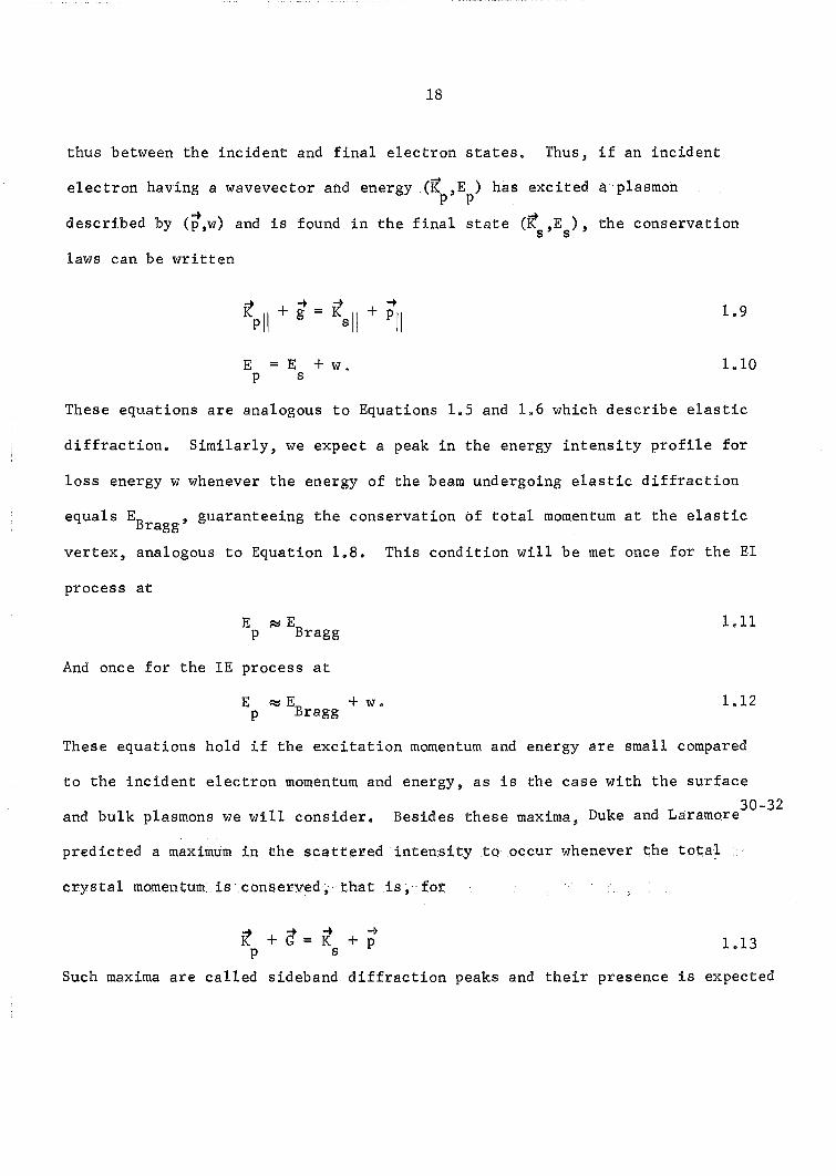
in the energy loss profiles. Figure 10 shows a series of loss profiles for a

-w -0 8 0
1--f
-0 0
1--f
20
25
W( 100) Bragg Scattering Only nw('p) = 5.0 + 4.44 (PIT+ PI) eV B=l./I=B'=o/'=0, 8=1r/2, A = 20A U = 1 eVA912
' (a) w=O (c) w = 8 eV
Figure 9. Theoretical energy intensity profiles
demonstrating sideband diffraction.
SP-902
-
-0 0
1--f
E .02 Tungsten ( 100)
~ (a) (!)
-0 g .01
Cl) .c. -
26
Energy Loss (b) Spectra
V0 = -8eV Aee= lOA
0
Ep= 68eV U = p.L eVA912
o Ep= 65 eV 8 = 1/1 = 81= 1/1'= 0 nw(1)}=(2p2+9)eV ~ o~-----+------4-------~----~------+-----~
--;;; .02 (d) (e) (f)
~ Ep= 80eV -c: 1-f Ep= 74eV Ep= 77eV Cl)
.::: .01 -c Cl)
ct:
10.0 9.0 10.0 9.0 10.0 11.0 Eloss (eV) SS-722
Figure 10. Theoretical energy loss profiles for a bulk
excitation demonstrating sideband diffraction.

27
bulk loss with a dispersion relation beginning at 9 eV. The motion in the peak
in the loss profile as the primary energy increases in value across the Bragg
energy at 68 eV is a result of different values of (t,w) satisfying the side-
band diffraction condition at different primary energies.
Figures 11 and 12 show a series of angular profiles calculated for
specular reflection at 15° from Al(lOO). These illustrate the expected differences
in the behavior of surface and bulk plasmons. The bulk plasmon angular profiles
show a doublet splitting for specific values of the primary energy where side- ·
band diffraction is undergone. The surface plasmon, on the other hand$ always
~ . shows a doublet splitting (for reasonable values of p > o and electron damp~ng)
for all values of E • This is the same conclusion as qualitatively derived p
from the Ewald diagram in Figure 7.

28
Angular Profiles- Bulk Plasmons
Plasmon Dispersion
"hw(eV) 16 l
I
f= l.06p2j
0 I
0 0 1.2 p (A-1)
Br=l5° w = 18eV
60
Energy Profile >. 8F=l5° -(f)
c Q) -c
1--1 ~----:=1~<-...-.~
SP-904
Figure 11. Theoretical angular profiles for a bulk
plasmon excitation demonstrating sideband diffraction.

29
Angular Profiles- Surface Plasmons
Plasmon Dispersion
nw(eV) I I I
11.1 I
0 r = L28p 11 !
0 ( o_1) 1.5 p11 A
8r=l5° w = 13eV
15 25 56 (degrees)
Figure 12. Theoretical angular profiles for a surface
plasmon excitation.
SP-905

30
2. APPARATUS AND EXPERLMENTAL PROCEDURE
2.1 Introduction
A medium resolution (~.5eV, 3.5°) scanning LEED apparatus has been
designed and developed in this laboratory by Professor F. M. Propst and Dr.
4 T. L. Cooper This instrument met the general criteria described in the
previous chapter in that it could measure the angular and energy distributions
of backscattered electrons. The design considerations and construction details
along with a description of general measurements on a W(lOO) surface are
described in the reference cited above. We emphasize here the modifications
made to the instrument, both to improve the operation and to include a different
target material, and we will briefly discuss the general operation of the
modified instrument together with the new experimental procedures.
The basic instrument, shown schematically in Figure 13, consists of
a four grid retarding field energy analyzer with a collimated Faraday collector,
electron gun, target assembly and electrostatic shielding. The target is
rotatable through 0 ~345 about an axis normal to its surface. The collector
is rotatable through an angle 8, 12°~ 8 < 90° about an axis which is per~ '
pendicular to the axis of rotation of the target and which intersects the
target surface, the incident beam direction and the axis of target rotation.
The angle 8 is the angular distance between the electrons detected by the
collector and the incident beam (which is normal to the target surface).
The combination of the two modes of rotation allow measurements to be made in
any backscattered direction, and the retarding grid analyzer can measure an

Suppressor
Shield
31
Bombardment Assembly Cathode
SR-464
Figure 13. Schematic of energy-angular distribution
instrument showing the basic components.

32
energy loss profile (or energy distribution) in any chosen direction.
2.2 Electron gun
The electron gun provides the incident or primary electron beam with
a well defined energy E • The gun is a simple triode design with cylindrical p
deflection units. The main lens is formed by the first two anodes and focuses
the crossover formed by the lens action of the control grid and first anode. A
voltage ratio of about 4:1 between the first two anodes is used to produce an
image of about 1 mm diameter at the target. Operating the lens in the
decelerating mode, beam currents of several microamperes at 100 eV could be
produced using a .0127 mm by 1.27 mm thoriated tungsten ribbon filament.
2.3 Target and Target Assembly
A new target holder was designed and built in order to use an aluminum
target. It is shown schematically in figure 14. The crystal is held in place
by clamping it against a slot in an Al block. This slot prevents the crystal
from rotating in the holder about an axis perpendicular to the face of the holder.
The block, clamp, and screw are made of ultra-high-purity aluminum to prevent
impurities from migrating to the target during annealing. This assembled block
is bolted to a copper block. A Mo spacer is inserted between the Cu and the
52 Al to prevent the possibility of the Al-Cu junction reaching a liquid phase
at 548°C (a possible annealing temperature). This system is then bolted against
two support rods which attach to the original target assembly. Directly behind
the target is a shielded tungsten filament for electron bombardment heating.

~ r> ·-. Stainless Steel Support Rods
OFHC Copper
33
Molybdenum
Ultra-High-Purity Aluminum
Crystal Target
Ultra-High- Purity Aluminum
SP-906
Figure 14. Details of the target holder.

34
The filament and target assembly are attached to a rotary feedthrough which
is alligned so that the axis of rotation is perpendicular to the target surface,
and which is capable of rotating the completed assembly through 345° with a
reproducibility of 1°.
The target is an ultra-high-purity (99.999%) Al single crystal which
was obtained from Professor M. Metzger53 It is 3.8 em x .9 em x .24 em in size
with a 2-56 clear hole drilled near the top to permit attachment to the Al
holder. This hole was EDM spark-cut so that little or no mechanical damage was
introduced into the experimental region. The surface preparation of the target
will be described in section 2.8.
Surrounding the target and attached to the target flange is the shield
assembly. This serves the major purpose of shielding the scattering and
measurement regions from external electric fields which would perturb the
incident and scattered electron trajectories. To complete the field free
region, there is a Helmholtz coil external to the system. Careful allignment
and current control has reduced the residual magnetic field in the target region
to less than 15 milligauss.
With the suppressor raised to a positive voltage with respect to
the shield, the majority of the electrons hitting the suppressor are trapped,
thus reducing the possibility of any electrons which have scattered from the
walls being detected by the analyzer.
The snout of the detector and the drift tube of the gun protrude
through a slot in the shield, and all these are kept at the same potential
as the target to insure a field free scattering region.

35
2.4. Detector
54 The original detector was a two grid retarding potential analyzer.
We have modified this to a four grid analyzer, shown schematically in figure 15.
The two new grids were wound with the existing precision instrurilent. 4 ·The grids
consist of 12.7 ].lm tungsten wire with a spacing of 63.5 ].lm brazed to a tungsten
plate. The retarding potential curve obtained with this type of analyzer is
differentiated55
' 56 by superimposing a small oscillating voltage on the retarding
voltage. The AC part of the signal to the collector is then proportional to
the current of electrons having energy E and energy spread dE. The energy E is
equal to the retarding voltage and the energy spread is basically the size of
the oscillating voltage. Only the general principles of the detector will be
given here, as the details of the design considerations and construction have
been given before. 4
Electrons enter the detector through the apertured snout, which
geometrically limits the direction the detected electrons to that originating
from the target. The aperatures both reduce the number of electrons detected
which have scattered from the snout and define the angular resolution of the
of the instrument. In this experiment, the operating angular resolution is
about 3.5°.
These columnated electrons pass through the entrance grid and arrive
in a retarding field region. The voltage responsible for this is called the
retarding voltage, VR, and is placed between the retarding and entrance grids.
Two grids are used to do the retarding because the resultant field is more
'f h 'd . Thi i h 1 · 57 d un1 orm across t e gr1 reg1on. s mproves t e energy reso ut1on an

Shielding Box Collector
Shielding Grid
••• •• •••
36
Collector Lead
Collector Shield
Insu Ia tors
Entrance Grid
yfh-~ .....J--"~<.Snout
Retarding Grids SP-903
Figure 15. Details of the four grid retarding field
energy analyzer.

37
4 qecreases the negative derivative effect - a change in the grid transparency as
a function of the electron energy. The operating energy resolution is about
.5 eV at 100 eV.
The electrons which energetically pass through the retarding grids
are accelerated to the shielding grid and pass through and strike the collector
where they are measured as a current. The loss of current from electrons
backscattering from the collector is minimized by (1) platinum-black plating
the collector plate to reduce secondary electron emission, and (2) applying a
"suppressor" voltage between the shielding grid and the collector.
The method of detecting the desired signal will be explained in
section 2.7.
2.5 Sputtering Ion Gun
Until recently, there had been no work done on clean single crystals
of aluminum. 58 In 1967, Jona perfected a technique for producing clean surfaces
of Al crystals. The method, explained in detail in section 2.9, involves
sputtering the crystal surface with argon ions. To use this method, we designed
and built a simple sputtering ion gun which would fit in the existing system.
It consists of a cylinder rolled from 16-mesh stainless steel screen
and closed on the end not facing the target. The axis of the tube makes an
0 angle of about 25 with the target normal and intersects the target at the
point where the incident electron beam does. The tube is 2.54 em in.diameter,
1.75 em in diameter, 1.75 em long and the front of the tube is 1.43 em from the
face of the target. Two tungsten filaments are supported outside the tube as

38
the source of the ionizing electrons. By applying a voltage between the hot
filaments and the tube, we are able to generate Ar+ ions in and around the tube.
These ions can then be attracted to the target by applying the proper voltage
between the target and the tube.
The ion spot produced on the target is about .8 em in diameter, or
about the width of the target and about eight times the size of the incident
electron beam. This final design was determined and the spot size measured by
sputtering an Al film from a Cu substrate with the experimental conditions as
used in the actual cleaning. Nonuniformity in the ion beam can be effectively
eliminated by rotating the target during sputtering.
2.6 Vacuum System
Once a clean experimental surface is established, it is necessary to
keep it uniformly clean during the period that measurements are taken. To
assure this, the experimental apparatus described·in.the previous subsections
is housed in the ultra-high vacuum system shown schematically in figure 16.
The vacuum chamber is pumped with two mercury diffusion pumps.in
series which are backed with a standard mechanical pump. The main diffusion
pump is kept free of any contaminents from the mechanical pump by the fore
diffusion pump. Backstreaming of gasses, including mercury, into the vacuum
chamber is greatly reduced by the thermoelectric baffle and two liquid nitrogen
cold traps in series with the main diffusion pump. The vacuum chamber is further
pumped with a titanium sublimation pump which is· directly attached to it. High
purity research (reagent) grade gasses are admitted to the system through a

0 0
L. N. Cold trap -L---1---
Main diffusion pump --1---+----
0 0
0 0
0 0
39
Sublimation pump
0 0
Slotted angle frame
~·-------"1"1- Water cooled baffle
- To mechanical pump
IL-------t---1- Fore diffusion pump
0 0
o" 6" 1211 ----
SR-194
Figure 16. Schematic of vacuum system.

40
gas manifold constructed from glass tubing and Granville-Phillips leak and
1/2-inch type C valves.
The system is bakeable to 450°C except for the baffle, diffusion pumps,
and gas bottles. -10 To achieve pressures in the low 10 Torr range, the chamber
and top trap (lower trap filled withliquid N2) are baked at 250°C for eight hours,
followed by an eight hour baking of the chamber by itself. After the chamber
0 cools the valve is closed and the two traps are baked at 250 C for eight hours,
concluding with a bake of the top trap only for another four hours. After the
traps are filled, the valve is opened and the sublimation pump flashed, a base
pressure of about 1 x 10-lO Torr is reached after about six hours. The background
4 gas was measured previously and was found to be almost all hydrogen.
2.7 Electronic Circuitry
Figure 17 shows a schematic of the electronic circuitry as it is set up
when measurements of either angular profiles or energy loss profiles are being
made. Capacitors used to eliminate 60 cycle and high frequency noise are not
shown.
The electron gun is connected to a simple voltage divider which keeps
the focusing voltage ratio constant as the primary beam energy is changed. All
electron gun elements are referenced to the drift tube, which is at ground
potential. The gun is shown operating in the decelerating mode. It can be
operated in the accelerating mode by simply interchanging the drift tube and
anode connections. The monoenergetic electron beam produced by the gun enters
the scattering area enclosed by the shield assembly. No detectable changes

Shield Assembly
Grid
Screening.......Grid
PAR CR4-A Preamp
PAR JB-5 Lock-In Amplifier
41
Hyper ion Model Si-10-12.5
L------111111----_..j Fluke Model 301C 0-lkV
'--+----"--~~ I -= I
PAR JB-5 Osci II a tor Output
L---------------, I I I I
Coupled to Retarding Voltage Potentiometer
Lambda Model 28 200-325V
I J-ti ~~~~d~e EAI Model 1130 X-Y Recorder
Coupled to Rotary Drive of Collector
.------II>IIJo
X-Input ~~~~~1~8 I I I I I
~---------------J SP-907
Figure 17. Schematic of electronic circuitry for energy
and angular measurements.

42
could be found by attracting scattered electrons to the suppressor, so the whole
shield assembly was kept at ground potential. The electrons then scatter from
the target, and some of these arrive at the snout of the collector. Both the
target and snout are at ground potential to insure a field free region for
scattering.
Passing through the entrance grid, the electrons arrive near the
retarding grid, which is kept at a variable voltage VR above ground. The
differential cross section is proportional to the derivitive of the collector
t . h V T h d . . . 55,56 . curren w~t respect to R' o measure t e er~v~t~ve, we super~mpose on
the retarding voltage a small oscillating voltage, 6 V sin wt. The AC component
of the collector current with frequency w is proportional, to first order in~ V,
to the cross section of the detected electrons with energy eVR. For the
measurements reported here, 6 V = .5 v, and w = 2kHz.
The collector current passes through a five megohm wire-wound resistor.
The voltage across this resistor is amplified by a PAR model CR4-A low noise
amplifier. This signal is then fed to a phase-sensitive PAR model JB-5 lock-in
amplifier, the output of which drives the y-axis of an EAI model 1130 x-y
recorder.
The x-axis of the recorder is driven by either of two potentiometers,
depending on the profile being measured. When angular profiles are measured,
the appropriate potentiometer used is directly coupled to the rotary feed-
through of the collector with a set of gears. When energy loss profiles are
measured, the potentiometer used is directly coupled to the potentiometer
which changes the retarding voltage. Both the collector and retarding voltage
potentiometer can be driven with a motor to assure smooth sweeps of each profile.

43
Figure 18 shows a schematic of the basic circuitry used when the
target is sputtered with argon ions.
2.8 Target Preparation
53 The ultra-high-purity aluminum crystal was spark cut to within 2
degrees of the (100) face. It was mechanically polished flat to less than ten
microns with silicon carbide grit. The surface was etched in a dilute solution
of HF between different grits to remove any work hardened material. The crystal
th h . 11 1' h d . 1 . 59 d f 0 h t (b 1 ) was en c em~ca y po ~s e ~n a so ut~on rna e up o e~g ty par s y vo ume
of phosphoric acid, fifteen parts of sulfuric acid, and five parts of nitric
acid. The crystal was polished for five minutes in this solution, which was
kept at 80 to 90°C. Following this, the crystal was electopolished flat in a
f . t 0 1 . 59 d f ew m~nu es ~n a so utlon rna e up o ninety-three parts (by volume) ethanol
and seven parts perchloric acid. Polishing was carried out with the bath
0 2 temperature at about -15 C and at a current density of .1 to .15 amp/em and
with constant, but mild, agitation. The perchloric acid polishing solution
was chosen over others primarily because it leaves60 a relatively thin ( ~30 A0
)
oxide layer on the surface. But because of the explosive nature of this solution,
61 we caution the reader to refer to Tegart before handling perchloric acid.
The polished target was then inserted in the target holder and placed
in the assembled vacuum system. To clean the target surface before taking any
58 measurements, we used the basic method perfected by Jona and subsequently
60 62 verified by others. ' The target first was submitted to a bombardment of
2 argon ions at 450 eV and about 3-5 w amp/em • This was followed by a vacuum

450V
Target
\ \ \ \ \ \ \ \...-,...
\ \ \ \
44
Ionizing Filament
l \ \ \
,.........>
I I I I I I I
I I
I I
I Ion Gun
Tube I
...__------w---t t--~..----11-1 ---o
350V 45V //
...... _______ ,.._ .,..,....,..,.
//
,.,." ...--""'
// /
//
Shield Assembly,} Collector Snout Electron Gun . Drift Tube
Figure 18. Schematic of electronic circuitry for
argon ion bombardment.
4----J
SP-959

45
0 anneal at 500 C for one hour. Five or six treatments consisting of bombardment
followed by annealing produced a clean surface. The crystal was rotated at
6°/min during ion bombardment to assure uniform cleaning. Every third cycle,
we extended the annealing time to two hours to assure that the damage introduced
by the ion bombardment was annealed away.
The target temperature had been calibrated by using two pieces of
1100 Al (gg.5% pure) which were machined to the same size as the experimental
crystal, polished, and separately placed in an identical target holder. A
chromel-alumel thermocouple was attached to the targets to measure their
temperatures. It was found that the temperatures could be reproduced within
0 0 ± 10 C at 500 C for the same target and between the two targets.
2.9 Criteria for Surface Cleanliness
There are many different criteria reported in the literature for
determining when a surface is clean or not. Some people use the clarity and
lack of secondary structure of ELEED pictures taken from a display instrument
as an indication of a clean surface. Others use the reproducibility of the
elastic energy intensity profile, while still others observe the Auger electron
spectra and note the presence or absence of peaks corresponding to different
elements. The major question which can be raised is to ask about the sensitivity
of each test.
The information gained from LEED will be related to the scattering
from a periodic array. Any adsorbate not in a periodic structure will only
contribute to the background of both the pictures and energy profiles. It

46
is generally accepted that extra ELEED spots or beams are probably detected with
periodic coverages of .1 to .25 of a monolayer. As far as this author can
determine, there have been no quantitative experiments relating diffuse background
changes to amounts of adsorbates.
One of the advantages of Auger analysis is that it can tell you the
kinds of absorbates (except for hydrogen and helium) on the surface. But
there have been relatively few calibration experiments63 which relate adsorbate
coverage to the strength of the corresponding Auger peak. One of the better
ones was done by Weber and Johnson, 64 in which they could deposit as little as
.01 monolayer of alkali metals on Ge and Si surfaces. They found they could
detect as little as .02 monolayer of Cs on Si using a standard three grid
retarding field analyzer. Their limiting factor was the size of the background
on which the Cs Auger peak was superposed. However, using the same type of
system, Weber and Peria65 reported they could only detect about .1 monolayer of
Cs on Si. Thus the sensitivity is probably instrument and technique dependent.
Of the calibration experiments referenced, only two deal with the study of a
gas on a surface. 66 Musket and Ferrante report a sensitivity of ,02 monolayer
of o2 adsorbed on W (110), assuming a saturation coverage of o2 equivalent to
one monolayer. Changing this assumption changes the measured sensitivity.
67 Similarly, Chang assumes an o2
saturation of .5 monolayer on Si (111) and
arrives at a sensitivity of ~ .005 monolayer.
Turning our attention to the work done on aluminum, we find that
J 48 'SS F 11 d S ' . 62 d B d ' 1 6 7 d 1 f ona, arre an omorJa1, an e a1r et. a • assume a c ean sur ace

47
on the basis of reproducible ELEED patterns and elastic energy profiles. But
Marsh60 combined ELEED patterns and Auger analysis and basically confirmed the
conclusions of Jona about surface cleanliness. However, after adding 02 to
the surface and then regenerating a reproducible ELEED pattern by heating the
crystal, Marsh found he could still measure a trace of o2
in the Auger spectra,
assuming a sensitivity of ~ .25 monolayer. This o2 could be removed with argon
bombardment. The results of Jona and Marsh yield a sticking coefficient of o2 on
-3 Al (100) of about 5 x 10 for low coverages. We will assume the sticking
coefficient of H2 to be about 3-4 times that of o2 , as is the case with o2 and
H2 adsorption on W. These assumptions are made for purposes of qualitative
discussion.
We have used four basic tests of the cleanliness of our target
surface. The least sensitive, but one which gives the order of magnitude of
cleanliness and is most attainable, was the reproducibility of the ELEED pattern
and the elastic energy profile. However, we found that the elastic diffuse
background changed a little faster than these as a function of time, hence
as a function of background gas adsorption. Noticeable changes occurred about
12 hours after cleaning, or, on the basis of the assumed sticking probabilities
and the measured pressure, after about .05 monolayer of background gas was
adsorbed.
We also observed the Auger spectra of the surface after multiple
cleanings and found no evidence of contaminents. 68 Robertson has recently
reported that the low energy Auger line of Al covered with approximately one
monolayer of oxygen is at 53-54 eV, while the Auger line of clean Al is at

66-67 eV.
48
63 The line at 54 eV is of the same value as that commonly reported
for "clean" Al.. Moreover, Jona 69 and this author, independently and at the
same time, had also measured the Auger line at 66 eV for clean Al. However,
the present appratus was not designed to do high sensitivity Auger work (better
than~ .1 monolayer sensitivity).
It is possible to monitor our surface cleanliness to coverages
better than the ~ .1 monolayer of o2
coverage provided by the Auger measurements
by using the technique of electron loss spectroscopy and the reproducibility
of the surface plasmon loss profiles. It has been found by Edwards 70 and this
author that when o2 is added to a clean surface of W, a new peak in the energy
loss profiles may be measured at 7 eV. This author determined that it is
most easily found near energy and angular conditions of Bragg resonances, and
its presence is detectable with about .05 monolayers of o2
on the surface,
using accepted values of the sticking probabilities. This loss peak was also
measured on the Al surface in the presence of o2
. If we assume the same
sensitivity as on W, we can say our surface is free of o2
to less than .05
monolayers.
The most sensitive test to change appears to be the reproducibility
of the surface plasmon angular and loss profiles. Changes in the peak positions
and intensities could be measured 6-8 hours after argon bombardment and
annealing, or with about .02 to .03 monolayer coverage of background (mostly
H2) gas, or ~' .01 monolayer of o2
• Again, we use the assumed values of the
sticking probabilities on Al. We could return the surface plasmon structures
to the original values after sputtering and annealing the surface.

49
Figure 19 shows a striking example of the types of changes measured
between a clean surface and one which had adsorbed some background gas amounting
to about .35 to .5 monolayers (using the assumed sticking probabilities and
pressure measurements). The loss peak at 11 eV has decreased in intensity and
shifted to 10 eV with the addition of gas on the surface. This is in general
21 . 19 20 agreement with the predictions of the theory and exper1ments ' done on Al
films. The loss profile of the clean Al surface could be reproduced by argon
bombardment and annealing of the "dirty" surface. One of the problems of using
this type of criteria for a measure of surface cleanliness is that the surface
plasmon losses from different primary beam energies and in different directions
reacted with different degrees of sensitivity to the same contamination. We
intend to do some work in the future to investigate the behavior of the surface
plasmon dispersion relation as a function of gas coverage.
All our measurements reported here as being taken on a clean surface
of Al were taken within 5-6 hours after each sputter-anneal cycle and in a
background pressure of ~ 1 - 2 x 10-lO Torr. Thus, we expect no more than .01
to .05 monolayer of adsorbate on the surface during our clean measurements,
2.10 Instrument Checkout
Before the instrument was assembled with the Al crystal, the new four
grid energy analyzer was checked for its operating characteristics with a new
W (100) target. 4 With the original two grid analyzer, Cooper reported seeing
large splittings in some of the inelastic angular profiles of electrons scattered
from W (100). The shapes of some of these splittings led him to conclude that
some of these were real, while others probably were experimental in nature.

50
I
Energy Loss Profiles I
' I AI (100) I
' g = (1,0) ' I Ep =56 eV ' I - 8 = 8Eiastic I
CJ) I - I c I :J
T I
-c ' Q) I N 1 U (X 50) =.0002 °/o I 0 j_ I
E I I
!>.- I 0 c \ I
......... \.I
>. 111 - I I CJ) I I c I I Q) I I - I I c
t-1 I I I I
I I (X 50)
Clean
----- ....... 0.4 Monolayer Background Gas I I I I
30 25 20 15 10 5 0 Energy Loss (eV)
SP-908
Figure 19. Energy loss profiles in the (10) diffraction
direction for a "clean" and "dirty" surface,

51
The addition of the third and fourth grids substantiated this
hypothesis. We were able to reproduce the angular splitting in some cases, but
were not able to in other cases. The majority of these cases agreed with the
conclusions of Cooper. Computer calculations of the electron trajectories
4 showed that the probable cause of the two grid splitting was an effect known
as the negative derivitive effect. That is, the effective transparency of the
grids increases over the optical transparency as the electrons which approach
the retarding grid approach zero energy. As they approach the grid, slow
moving electrons which would have collided with a grid wire had they maintained
a straight line path, are deflected away from the wire by the component of the
electric field which is parallel to the grid plane and which exists (with any
strength) near the grid wires. To eliminate this effect, the new grids were
wound with a wire spacing of one-half the original wire spacing, and placed
together so the wires of one were perpendicular to the wires of the other in
the retarding plane. Besides eliminating the negative derivitive effect, the
n~w grids improved the energy resolution of the instrument. This improvement
was noted in the halfwidth of the elastic energy peak and in the halfwidth of
the peaks in the elastic angular profiles.

52
3. DATA PRESENTATION AND DISCUSSION
This chapter is organized into two parts: (1) a presentation of
the experimental measurements together with a general discussion of the results,
(2) a detailed comparison of theoretical profiles and experimental measurements.
The experimental measurements will be displayed in the three forms as
discussed in chapter 1. Figure 20 schematically reminds us that the three forms
are energy intensity profiles, energy loss profiles, and angular profiles. The
energy intensity profiles measure the scattered intensity as a function of the
incident or primary energy. The energy loss profiles measure the scattered
intensity as a function of the energy loss, and the angular profiles measure
the intensity as a function of the scattered polar angle or collector angle. In
each case, the other parameters are held constant.
The profiles will be presented in a set of normalized units, so that
the diffracted beam intensities can be compared with each other and with the
intensity of the incident beam. The method for making these comparisons, the
first of their kind for inelastically diffracted electrons, together with an
intensity analysis is given in the next subsection.
The theoretical profiles used in the last subsection were calculated
.36 71 by Duke and Bagch1 ' of the Department of Physics, University of Illinois. '

Energy Intensity Profile Variable: Ep
Energy Loss Profile
Variable: w
Angular Profile
Variable : 8
53
I
n I~w 0
Figure 20. Schematic of the three forms of
presentation of the experimental measurementso
55-927

54
3.1 Measurement of the Absolute Intensity
The object of this section is to determine the percentage of electrons
scattered into a particular region of the energy-angle space, and then use this
as a calibration for the rest of the measurements. To accomplish this, we must
perform three tasks. First, we must measure the total electron current incident
on the target. Second, we must measure the electron current scattered into a
particular beam in the desired energy-angle space. Finally, we must compare the
experimental measurement (detector output) of this beam profile with the
scattered percentage of incident current to get a conversion factor for the
electronic outputo
Figure 21 shows the measurements made in the calibration experiment
to determine the desired conversion factor. In this calibration run, the
-6 incident electron current to the target, I0
) was measured at 5.0 x 10 amperes,
which is the sum of the target current and the current to the electronic
shielding. Since the electron gun is the only source of electrons, and since
the current is conserved, this measurement gives the correct incident current.
We next took an angular profile of the elastically scattered elect~ons, as
shown in Figure 21 (a). To measure the currents, we located our collector at
0 34 , to correspond to the peak in the elastic angular profile. We then measured
the retarding energy curve and the energy loss profile, as shown in the other
two panels. It is easy to show that with a collector of energy acceptance
width approximately equal to the incident electron beam width (about 1 eV in
our case) that the total scattered elastic current is approximatelx the current
at a loss energy of 1.5 times the energy width. In these measurements we found
I (Elastic) -8 ::; .1 x 10 A.

10 = 5Xl0-6 Amp Ep=ll5eV
g = (1 0)
(a) Collector Current vs Retarding Potential for Collector Angle, 8 of 34°
(b) Angular Profile of Elastic Electrons ( w = 0)
(c) Energy Loss Profile for 8 =34° Profile Resu Its from Differentiation of Retarding Potential Curve, (b)
(/)
:!:: 0.76 c ;:::,
"'0 Q) N
0 E lo-0 c
(/)
c Q) -c ~
55
I( ER) -2
(/)
a.. E 0 0 c 0 c
-c ~ 1 "-;:::, u "-0 -u Q)
0 u
Figure 21. Experimental measurements necessary to
calibrate the intensity of the scattered electrons.
(/) -0.76 ·c: ;:::,
"'0 Q) N
0 E lo-0 c
(/)
c Q) -c ~
SP-949

56
The measured height of the elastic beam is .76 units; these units
are applicable when the values of all variables such as amplifier gain, etc.,
set in the calibration experiment are used. Then an experimental height of .76
-8 -6 units corresponds to a percentage reflection equal to ,l x 10 /5 x 10 or
.02% I . Thus, one unit equals approximately .026% I • This factor has been 0 0
applied to all the measurements, with proper account being taken for amplifier
gain, etc. To make the measurements easier, we will convert the scale to what
we will call "normalized units'', in which one normalized unit equals .01% I • 0
If a curve has been amplified for clarity, this will be denoted on the profile
as a gain in parenthesis after the fixed variable, such as E =lOOeV(xlO), p
indicating that the particular profile is for a primary energy of 100 eV and
is shown amplified by a factor of 10. For convenience, we have also included
the amplification factor on the intensity scale shown on the experimental
profiles. Thus the absolute intensity of each curve can be read directly.

57
3.2 Energy Intensity Profiles
This section will be devoted to the discussion of the experimental
measurements of the elastic and inelastic energy intensity profiles. The
profiles to be discussed are those of the (10) and (11) diffraction beams
resulting from the diffraction of electrons incident normally on a clean
surface of Al(lOO). In obtaining the energy intensity profiles, a series of
angular profiles was taken over the range of incident electron energies for
each desired loss energy. The intensity was then measured at the desired
collector angle by subtracting the extrapolated incoherent background and
normalizing to unit incident beam current. The inelastic intensity for each
incident energy was measured at the collector angle at which the elastic
angular profile at that incident energy was a m&ximum. This collector angle
is what we called eEl i in the first chapter. Figures 22 and 23 show the ast c
measured elastic (w=O) and inelastic (w=8-18 eV) energy intensity profiles for
the (10) and (11) diffraction beams respectively.
The extrapolation was done by smoothly joining the profiles on each
side of the diffraction peak. The incoherent background possibly consisted of
electrons which had excited single particle-hole excitations and phonons and
of electrons which excited plasmons, but which scattered incoherently from
regions of imperfection of the crystal surface. While no detailed study was
made of the effect, it was noted that this background generally increased as
gas became adsorbed on the surface.

-(/) -c: ::J
"'0 Q) N
0 E '-0 c:
-(/) c: Q) -c:
1-f
(/)
Q)
> ..5 0 'Q)
N
l 18
16
14
12
10
8
58
Elastic and Inelastic Intensity Profiles AI (100) g = ( 1, 0)
8 = BEiastic
Primary Energy
I lu(X1)=.01% lu (X 50) =.0002% lu (XlOO) = .0001%
16 (X 50)
14(X50)
12(X 50)
10 (X 50)
8 ( X50)
0 (X 1)
SP-811
Figure 22. Elastic and inelastic energy intensity profiles
for the (10) diffraction beam. The intensity
unit is labeled for each scale factor used.

-U) -c ~
"0 (]) N
c E !... 0 c ->. -U)
c (]) -c
1-1
Elastic and Inelastic Intensity Profiles
AI (100) g = ( l, l) I lu (xl) =.01 °/o lu (x 20) = .0005% 1 U (X 50) = . 0002 % 8 = BEiastic
U)
(])
> .3 0 !... Q)
N
+ 18
16
14
12
10
8
0
Figure 23,
90 110 130 150 170 Primary Energy (eV) sp-a
Elastic and inelastic energy intensity pro'riles
for the (11) diffraction beam.

60
3.2.1 Elastic Energy Intensity Profiles
The (10) elastic energy intensity profile has two major peaks at
54 and 107 eV. The (11) profile has three major peaks at 43, 86 and 152 eV.
Each profile has some minor peaks we will discuss later. The first thing to
notice is that the major peaks in each profile are distinct, well separated
in energy, and of a narrow halfwidth (10-12 eV). These peaks correspond to
classical Bragg peaks resulting from a single scattering if an inner potential
correction of about 14 eV is used. This is most easily seen by comparing our
experimental peak locations with those predicted theoretically by Laramore and
Duke72
and found in Table 1. The inner potential of 14 eV locates all of our
experimental peaks within 1 eV except for one which is within 2 eV.
48 We can also compare our elastic measurements with those of Jona and
F 11 d S 0 .62 arre an omorJa1 . Their experimentally determined peak locations are also
found in Table 1. For the most part, the agreement with the work of Jona is
very good, while that with Farrell and Somorjai is adequate. It should be noted
that both Jona and Farrell and Somorjai used spot photometers and display type
LEED screens for their experimental measurements. Farrell and Somorjai did
not normalize their curves to eliminate variations in incident electron current,
and both they and Jona did not eliminate the diffuse and incoherent elastic
background and could not make absolute intensity measurements. With this in
mind, we can at best only approximately compare our peak shapes with those of
Jona. Doing this, it is found that the relative heights of the (li) and (10)
peaks compare quite well, although Jona's (10) peak at 84 eV is much more

61
Table 1. Comparison between experimentally observed and theoretically
Jona 48
(11) beam:
46
90
151
(10) beam:
56
84
105
predicted positions of the principal peaks (in eV) in the elastic
energy intensity profiles of the (11) and (10) diffraction beams
from Al(lOO). VT is the inner potential correction. 1.
Experimental Theoretical
Farrell and s .. 62 omorJal This work Laramore and Duke 72
v =14 I
v1=16.7
43 43 40
88 86 87 84
143 152 151 148
55 54 53 50
74 (75) 75 73
98 107 105 102

62
pronounced than ours. However, the full width at half maximum of Jona's peaks
are about 20 eV, a factor of two larger than ours. This might be an effect of
68 our having a cleaner surface or to our subtracting the incoherent background.
The peak in the (10) profile at 75 eV can be seen more clearly on a
semi-log plot. At this point, though, all that is important to notice is that
this peak is almost negligable compared to the two prominent peaks. This will
be discussed in more detail in the next subsection on the inelastic profiles.
We should also note the presence of some secondary structure in the
profiles. There are two low energy peaks in the (10) beam profile at 33 and
40 eV. The (11) profile shows two peaks at 54 and 63c5 eV and some less
prominent peaks at 112, 121 and 130 eV. Jona's profiles show these secondary
peaks near 34 and 42 eV in the (10) profile and at 68 and 120 eV in the (11)
profile. These are probably multiple scattering resonances. We discuss
the nature of the 63.5 eV peak in more detail in the next subsection, as we
get a clue to its nature from the inelastic profiles. We compare the elastic
intensity profiles with the theoretical profiles in more detail in Section 3.5.

63
3.2.2. Inelastic Energy Intensity Profiles
At this point, it is appropriate to recall the discussion given in the
first chapter concerning inelastic low energy electron diffraction (ILEED).
The two step model of ILEED says that the electron may undergo elastic
diffraction from the lattice and inelastic scattering, such as by plasmon
excitation, in either sequence. This is what we called EI and IE scattering.
In the inelastic energy profiles, we expect one peak to occur at about the
Bragg energy when electrons undergo EI scattering. and one peak at the Bragg
energy plus the loss energy when IE scattering occurs. In addition, Duke and
Laramore predicted that these two peaks split into four peaks when the sum of
the incident electron momentum, final electron momentum and the excitation
momentum (of a bulk loss mode) equals a reciprocal lattice vector of the solid
(assuming that the peaks are resolvable). This effect is demonstrated in Figure 9.
An examination of the inelastic intensity profiles for both diffraction
beams, Figures 22 and 23, shows that the structure for each loss energy is
closely correlated with the structure in the corresponding elastic profile.
That is, the gross structure in the inelastic profile occurs at about the same
energies as the structure in the elastic profile. The dotted region of the
profiles was that region in which the inelastic diffraction peaks were not
defined well enough to permit an accurate measurement of their intensity. The
dotted line represents the estimated intensity in this region.
Confining our attention to the energy region around the major peaks
in the elastic profile, we first note that a peak occurs in the inelastic profiles

64
at about the energy that the elastic profile has a Bragg peak (within- 1 eV).
This inealstic peak at EB is principally associated with those electrons ragg
whose scattering amplitude for elastic diffraction followed by an inelastic
scattering (EI) is large. Around each of these peaks at the Bragg energies,
there occur other peaks in the inelastic profile, their number, energy position
and intensity depending on the particular loss energy and primary energy.
We expect to see a peak in the inelastic profile for loss energy w
at E + w which is principally associated with those electrons whose Bragg
scattering amplitude for an inelastic scattering followed by elastic diffraction
is large (IE scattering). Indeed, peaks are experimentally observed at E Bragg
+ w within ± 1 and 2 eV for a majority of the inelastic energy profiles in
both the (10) and (11) diffraction beams. The clearest example of"".this is
seen around the (11) Bragg peak at 86 eV. For electron losses between 10 and
16 eV, we find a prominent peak at 86 eV, corresponding to EI scattering, and
a second peak located above this which moves away in energy as the loss energy
increases, corresponding to IE scattering.
However, for a loss energy of 18 eV, the inelastic profile around
E =86 eV has become a four peaked structure. As the electrons which have lost p
18 eV are those which have primarily excited bulk plasmons, the presence of
four peaks is an indication of sideband diffraction. This will be more fully
substantiated in the section on angular profiles. Again, if we refer to Figure
9, we expect this four peaked structure in the inelastic energy profile to
be an effect of sideband diffraction. There are also other regions of both
beam profiles which show multiple peaked structures for the inelastics, for
instance, around the (11) Bragg peak at 152 eV and around the (10) Bragg peak
at 107 eV. While some of the structure of the 18 eV profile near 152 eV

65
might be due to sideband diffraction, the presence of a third peak in the
profiles of the 8 and 10 eV losses suggests that multiple scattering effects
might be the primary cause. This is plausible, as these higher energy electrons
will penetrate more deeply into the crystal, and hence will "see" more ion
cores with which they may interact. However, there are no multiple-scattering
peaks in the elastic profile near this primary energy, which tends to cast some
doubt on this explanation. The profile of the 18 eV loss in the neighborhood
of the (10) 107 eV Bragg peak has four peaks at EP = 106, 113~ 124, and 128 eV.
The 106 and 124 eV peak would correspond to E + w. The 113 eV structure Bragg
is present in some of the other profiles and is probably a multiple scattering
resonance, while the peak at 128 eV is not seen in the other profiles and might
be due to sideband diffraction.
There are a number of interesting phenomena present in the inelastic
profiles. First, the rather prominent peak in the elastic (11) profile at 63.5
eV is present in the inelastic profiles of w = 14, 16, and 18 eV. Since the peak
is present for surface plasmon losses, and not for the bulk plasmons, we are
first led to the speculation that the 63 eV peak is a surface phenomenon in
which the electron beam does not penetrate into the crystal deep enough to
make excitation of a bulk plasmon probable.
We consider such a surface phenomenon to occur when, in a multiple-
scattered electron beam, one of the intermediate electron beams propagates along
the surface, and the wavelength of this intermediate beam is some intergal
multiple of the distance between the scattering ion-cores. On the surface, the
distance between the ions in the ~0) direction is 2.86 1. An electron with an

66
energy of 74 eV has a wavelength of about 1~43 A, exactly one-half that of the
ion core separation. Thus, assuming a reasonable value for the inner potential
of about 11 eV, it is possible that the 63 eV peak may be due to a multiple
scattering resonance along the (10) direction in which the intermediate beam
propagates along the surface. This conclusion is further strengthened by an
examination of the (10) elastic and inelastic profiles. First, the (10)
elastic profile has a definite shoulder near 63 eV. Second~ the inelastic
profiles for losses between 10 and 16 eV have peaks at 63 eV. These peaks are
probably not due to IE diffraction associated with the Bragg peak at 54 eV~ as
these other peaks do not move as the loss energy is varied. If we examine the
angular profiles and the loss profiles at primary energies around 63 eV~ we
find that the loss meahcnisms are almost entirely surface plasmons, explaining
the presence of the 63 eV peak in the w = 14 and 16 eV energy profiles.
Taking all this behavior into account, it becomes reasonable to
infer that the 63 eV peak in the (11) energy profile is indeed a multiple
scattering resonance along the surface. We shall also see the presence of a
peak in the theoretical profiles near 62 eV which is a multiple scattering peak.
With this in mind, we can now question the nature of the peaks in the
(10) inelastic energy profiles near a primary energy of 74 eV. These peaks
may either be IE peaks associated with the 63 eV peak, or EI peaks associated
with the small elastic peak at 75 eV, or some other phenomenon. It is
unlikely that these are EI scatterings~ as the elastic peak is not readily
seen on such a linear plot, and we would not expect the inelastic structure
associated with this to be so large, as it happens for no other energy region
we have examined. Because the 10, 12, and 14 eV peaks move upward in primary

67
energy, we can more reasonably infer that these peaks are the IE scattering
of the surface resonance. It then remains a mystery as to why the w = 16 eV
peak is located at the same energy as the w = 10 eV peak is.
Another interesting observation is that there is no secondary IE
structure associated with the diffraction peak at 43 eV in the (11) beam. All
the inelastic profiles have only one peak (an EI peak), except for a possible
shoulder for w = 18 eV. It is possible that the other structure is m:ixed with
that of the elastic peak -54 eV, although it doesn't appear likely after
examining the profiles.
It is more likely that most of the intensity of the plasmon losses
can be found at angles away from A-1
. • This can be explained by remembering VI:!; ast1.c
that the excitation wavevector for a given loss energy has remained the same~
while the wavevectors of the electrons near 43 eV energy are considerably smaller
than those of electrons near 86 eV or 142 eV. A vector diagram which conserves
momentum parallel to the surface demonstrates that the angular spread in the
resulting inelastic electrons at lower energies will be larger than the angular
spread at higher energies. This is measured experimentally and can be seen
in the angular profiles in section 3.4.

68
3.3 Energy Loss Profiles
In this section, we will briefly survey the types of results
measured in the energy loss profiles ,
Figure 24 shows a series of energy loss profiles. As we discussed
in section lo3, the prominent peak near w = 10 eV corresponds to the excitation
of a surface plasmon, the peak near 15 eV to the excitation of a bulk plasmon.
As shown in this figure, we have also measured the presence of a loss peak
at 26 eV and another at w 31 eV. The 26 eV loss possibly corresponds to the
excitation of both a bulk and a surface plasmon, while that at 31 eV is possibly
that of two bulk excitations. These higher energy losses became more prominent
as the energy of the incident electrons was increased. Although we never
painstakingly searched for it, we never observed a 20 eV loss peak, which
would correspond to the excitation of two surface plasmons.
We also have observed a series of loss peaks between 4.0 and 6.0 eV,
and one at - 8. 0 eV. Figure 25 shows three energy loss profiles taken in the
(10) diffraction direction at different collector angles. The peak in the
angular distribution of the 56 eV elastic electrons occurred at a collector
1 f 310. ang e o Besides the surface and bulk plasmon losses, \-Je see a loss peak
at 4 eV, a shoulder at - 5.5 eV, and a shoulder at - 8.0 eV each occurring on
a different profile. We believe that the 4 to 6 eV losses are due to a single
loss mechanism. Small changes in the collector angle moved the position of the
loss peak a great deal within this energy loss range. This is evident from the
figure •. The presence of these losses also was observed only in a primary energy

30
Energy Loss Profiles A I ( 100) g = ( 1, 0) Ep=56eV
lu (X 50)= .0002°/o
, I I I I I I I I I I
' I I
,' I
/ /~
#' ......
.,_.I'
I I
I
\ \ \
' \ ' \ \ \ \
~ ......... ..,.,.," e = 2s ( x 5o) ..,.,,.., ,.., ....,.......-- "e =3l(x5o)
I I
I I I
' I I
' I
25 20 15 10 5
Figure 24. Energy Loss (eV)
Energy loss profiles for different primary
showing the bulk and surface plasmons.
.......... (/) -c:: :l
"'C (l,) N
c E '-0 c::
-....
>. -(/)
c (l,) -c::
t--1
0
SP-870 energies

Energy Loss Profiles A I (100) g = (1 I 1)
8 = BEiastic
-95
90
Ilu ( 10) = .001% lu (X 20) = .0005 °/o lu (x50) = .0002%
80(Xl0)
• SP-879 Figure 25. Energy loss profiles for a pn.mary energy of 56 eV
and different collector angles. 0
eEl t' = 31 • as ~c

71
range around the (10) Bragg energy at 54 eV. These facts lead to the speculation
that these peaks are a phenomena of sideband diffraction for a highly
angularly dependent bulk excitation such as an indirect interband transition.
Unfortunately, the angular and energy resolution of the present instrument
prohibits an accurate measurement of the losses' behavior as a function of the
experimental variables and hence a determination of their nature.
The nature of the 8 eV shoulder is even more mysterious. Its
presence is measured only within! 1° of the elastic peak and within± 2 eV
of 56 eV primary energy. It was found in a detailed search only after
observation of the peculiar doublet in the w = 8 eV angular profile, as seen
in Figure 26. As a loss of 8 eV is below the surface plasmon threshold (-10 eV),
the pronounced angular doublet is hard to justify without the presence of
another loss mechanism. But its highly localized nature in energy and angle
makes it impossible to determine its nature with this instrument.
In section 2.9, we briefly described the behavior of the energy loss
profiles as a function of surface cleanliness. Figure 19 demonstrated that a
small addition of contamination on the surface leads to a rather significant
change in the loss profile - both in intensity and peak shape and position.
However, it was not the purpose of this work to make a detailed and systematic
study of the effects of gas adsorption on the inelastic profiles. We have found,
though, that the effects are significant and warrant future study.
Finally we shall look at the effects of different diffraction
conditions on the energy loss profiles. Figure 27 shows a series of energy

0
72
W = 0 (X1)
1 U ( X 1 ) = . 01 °/o lu(X50) =.0002°/o
10 30 40 50 60 Collector Angle,e (degrees) SP-865
Figure 26. Angular profiles at 56 eV primary energy for electron
loss energies of 0 and 8 eV.

Energy Loss Profiles AI ( 100) g = (11)
8 = 8elastic - 2.5o
(/)
a:; > 3 0
~
~ 100
95
90
80 (XlO)
73
Energy Loss Profiles AI (100) Energy Loss Profiles AI (100) g=(11) g=(l1)
8 = 8elastic 8 = Belastic + 2.5o
T T 1u lu j_ l_
80 (Xl0)
85 so----~~~~~~~~~~--~~~~~~~~~0----~~~~~-7.~~~
Energy Loss Energy Loss Energy Loss SP-893
Figure 27. Series of energy loss profiles in the (11) diffraction beam
for different primary energies, E , and collector angles e. p

74
loss profiles taken at different primary energies (E = 80 - 100 eV) and at p
three different relative collector angles. Recalling the discussion in
section 1.4.1, we have defined eEl . as the angle at which the elastic ast~c
angular profile is a maximum, In other words, this is the angle relative to
the surface normal at which the wavevector of the diffracted electron intersects
the reciprocal lattice rod in an Ewald construction. We have chosen the various
primary energies so as to encompass the (11) Bragg energy at 86 eV. Recalling
Figure 24, we see that this choice of primary energies moves from a range
primarily of EI diffraction to a range primarily of IE diffraction.
The first thing to be noted is the relative growth and decay of the
surface and bulk plasmons as a function of primary energy and scattering angle.
First, for the collector angles constant with respect to eEl . , we note that ast~c
for primary energies below the Bragg energy, there is a large surface plasmon
loss peak at w = 10 eV and only a shoulder of a bulk plasmon loss. As the
incident energy increases through the Bragg energy, the bulk plasmon loss grows
relative to the surface plasmon until atE = 100 eV, there is a large bulk p
plasmon loss peak at w = 15 eV and only a shoulder of a surface plasmon loss.
The rate of increase and decrease is dependent on the angle relative to
eEl t' , as can easily be seen by comparing the three panels. This can also as ~c
be seen by comparing the profiles for a constant incident energy, for example,
those of Ep = 95 eV. For a collector angle less than eElastic' the loss
profile consists of a large surface plasmon loss and a shoulder of a bulk

plasmon loss.
75
As the angle is moved to angles greater than eEl i , the ast c
loss profile consists of a large bulk plasmon loss and a shoulder of a surface
plasmon loss.
Careful examination of the loss profiles show that the position of
the peaks are a function of the primary energy. For instance, at 6 the Elastic'
surface plasmon loss peak is at 10 eV for E = 80 eV and at about 11 eV for p
E = 95 eV. One can reasonably ask whether this shift is a real change as a p
function of different diffraction conditions, or whether it is an apparent
change caused by the addition of a large bulk plasmon peak located near the
surface plasmon. If we assume that the loss peaks are Gaussian curves with
widths equal to the experimental widths (-2 eV) and separated by 5 eV then a
numerical calculation shows that the addition of a second peak which is equal
in height to the first will shift the first peak position by about .3 eV. Thus,
the 1 eV experimental shift is probably a real shift which is a function of
the incident electron energy. That this shift is real is further substantiated
by comparison with the theoretical profiles as seen in Figure 44 of Section 3.5.

76
3.4 Angular Profiles
This section will be devoted to an analysis of the measured angular
profiles. First, it is worthwhile to review some of the qualitative predictions
made in section 1.4. The angular profiles of the surface plasmons are expected
to consist of doublets due to the directional limitations of the excitation
along the surface (recall Figures 7 and 12). The angular profiles of the bulk
plasmone are expected to be single peaked, except in regions of sideband
diffraction, where this peak splits into two peaks (recall Figures 8 and 11).
To distinguish which loss energies are associated with a particular
excitation, it is necessary to study the energy loss profiles, such as Figure
27. In general, it appears that the losses between - 9 and - 12 eV are
associated with purely surface plasmons, losses between - 16 and 19 eV with
bulk plasmons, and losses between ~ 13 and 15 eV can be associated with both
bulk and surface plasmons. We can see from Figure 27 that the relative strength
of the excitations in the 13 to 15 eV loss regions is dependent on both the
primary energy and the angle relative to e . We will refer to this Elastic
figure as we identify the structure in the various angular profiles.
Initially we concentrate our attention on electrons diffracted
into the (11) plane in the region of the (11) Bragg peak at 86 eV. We will do
this because this Bragg peak is the most intense, and the inelastic structure
is the most pronounced in this region,
Figure 28 shows a series of angular profiles at a constant primary
energy (E = 86 eV). Note that the elastic profile (w=O) is symmetrical and p

If) -c ::::1
" (])
.!:::! 0 E ._ 0 c::
.~ If)
c .2! c:: ......
Angular Profiles AI (100), g =(1,1) Ep = 86 eV
2 (])
> j 0 .... (])
N
~ 19
15
14
13
12
11
9,10
8
10 (XlO)
9 (XlO)
I lu(xl) =.01% lu(XlO)=.OOl% lu(x 20) =.0005%
Collector
77
Figure 28. Angular profiles for constant primary
energy (86 eV) and different loss energies.

78
well localized in angle in what is commonly called a diffraction beam. If we
examine the inelastic profiles (w#O), we see that they too are found in
localized beams which are located very near the elastic beam. This is a
consequence of inelastic two-step diffraction. Without a diffraction from
the lattice, we would not expect to find the inelastics so well localized in
angle. But there are dynamical scattering effects present, as can be seen in
the internal structure of the inelastic profiles. These can be seen more
clearly in the next set of figures.
Figures 29 and 30 show a series of angular profiles for losses of
10 and 12 eV respectively, taken at a number of different primary energies.
The range of primary energies includes values both above and below the (11)
Bragg energy of 86 eV. The black dot on each profile indicates the position
of the peak in the elastic angular profile for that particular incident energy.
The first thing to note is that the inelastic profiles are all peaked in
approximately the direction of the elastic diffraction beam. Thus, the
diffraction effect we saw in Figure 28 for one primary energy holds for a
number of primary energies which span a range of different diffraction
conditions. In addition to the gross structure, there is a large amount of
substructure present.
The angular profiles for both the 10 and 12 eV losses show the same
type of behavior. At incident energies below and near EB , the angular ragg
profiles are single peaked to the low angle side of the elastic peak. As the
incident energy approaches E + w, the profile splits into two peaks, with Bragg

(/) +-c::: ::J
"0 Q) N
0 E >... 0 c:::
>. --(/) c::: Q) -+-c::: 1-i
0
Angular Profiles AI (lQO) g = (1, l) w = 10 eV
(/)
Q)
> Q) _I
0 .._ Q)
N
+ 104 102
101 100
99
98
96
94
92
86
79
I lu(XlO) =.001% lu(X20)=.0005% lu(X 50) =.0002%
102(X20).
101 (X 50)
lOO(X 20)
99(X20)
98 (X 20)
96(X 20)
94(X20)
92(X.20)
80
SP-868
F:i.gure 29. Inelastic angular profiles, w = 10 eV, in the (11)
direction. Each black dot indicates the position of
aEl t' for each primary energy. · as 1c

c
Angular Profiles Al{lOO) g=(l,l) w = 12 eV
(/)
Q) > j 0 loo... Q)
N
~
8C
I 1 U (X 10) = . 001% lu ( x 20) = .0005%
::3 102(X20)
-g 102 N
0 E \... 0 c
(/)
c Q) -c
1----j
0
101
100
99
98
96
94
92 90
88
86
Figure 30.
101(X20)
lOO(x 20)
99 (X 20)
98(X20)
96(X 20)
94(X20)
92 (X 20) 90(Xl0)
88 (X 10)
20 30 40 50 60 70 80 Collector Anale 8 . (dearees) . sP-e.s1 Inelast1c angulgr prof1les,~ = 12 eV, 1n the ~ 1)
direction. Each black dot indicates the position of
eEl . for each primary energy. ast1c

81
the high angle peak becoming dominant as the incident energy is increased.
With further increases, the profile becomes a single peaked structure again,
but with the peak located on the high angle side of the elastic peak.
This behavior is not exactly that expected of surface plasmon
angular profiles if one considers a purely kinematic model of inelastic
diffraction. This type of model, such as given by the Ewald collision diagram
in Figure 7, predicts a sharp double peaked structure in the inelastic angular
profiles for all incident energies. Even a quantum field theoretical treatment
(QFT) 31
,32
) whose initial results are shown in Figure 12, predicts a doublet
structure at all energies. But as we see in this figure, and as will be seen
in the next section, the QFT treatment also predicts that large intensity
differences can occur between the two peaks. Large internal damping effects,
such as through decreased plasmon lifetimes, can then make these two peaks
appear as a single peak. If the surface plasmons in question have a small
wavevector, the finite angular resolution can make even two peaks of equal
intensity appear as a singlet. But it should be noted again that the doublet
structure is seen over a range of primary energies for the surface plasmon
angular profiles.
Looking at the energy loss profiles, Figure 27, it appears that the
angular profiles of the 16 and 18 eV losses should be representative of bulk
plasmon angular profiles. Figures 31 and 32 show a series of angular profiles
for these two losses which were taken over a range of primary energies which
includes the 86 eV Bragg energy.

(f) +-
c:: ::::l
"'0 Q) N
0 E ..... 0 c::
>.
(f) c:: Q) +-c::
H
0
Ep= 108 {X20)
(f)
Q)
> .3 0 .... Q)
N
+ 108
106
104
102
100
98
96
94
92
90 88
86
84
10 20
82
30
Angular Profiles,
AI (100), g= (1,1), w=16 eV
Figure 31. Collector Angte 8 (dearees)
Inelastic angul~r profiles, w = l~p~Ys, in the
(11) direction. Each black dot indicates the position of
8 for each primary energy. Elastic

....... (f) ..... c:: ::I
"'0 Q) N
0 E .... 0 c::
>. ..... (f)
c:: Q) ..... c::
H
Angular Profiles
Ep = 112 (X50)
(f)
Q)
> Q) _J
0 .... Q)
N
~
108
106
105
101
100
83
AI (100), g= (1,1), w=l8 eV
I lu(x 20) = .0005% lu(x50) =.0002%
60
Figure 32. Collector Angle, 8 (degrees)
Inelastic angular profiles, w = 18 eV~ann the (11)
direction. Each black dot indicates the position of
eEl t" for each primary energy. as ~c

84
It should be noted first that the profiles are more or less localized
around the elastic beam, indicating inelastic diffraction. As in the profiles
of the surface plasmons, these angular profiles also display the motion of the
inelastic peak from the low angle side to the high angle side of the elastic
peak. The behavior of the diffraction substructure is an experimental
verification of sideband diffraction. As the incident energy sweeps in value
h B h f 'l h 1 d' d 32 across t e ragg energy, t e pro L es c ange exact y as pre Lcte . The
profile begins as a singlet peak, which changes to a large doublet as the
incident energy E increases. The high angle peak decreases in size relative p
to the low angle one until at some E < (E + w), there is only a singlet p Bragg
peak remaining. The singlet then splits into a doublet for larger energy,
and as the incident energy is increased further, the profile returns to a small
singlet. However, the presence of a doublet peak is not necessarily evidence of
sideband diffraction. Certain structure can be associated with a surface
plasmon loss and hence the cause of an apparent splitting. This will be
discussed in more detail in the following paragraphs and in the next section
where we compare experimental and theoretical profiles.
As mentioned before, we expect that the profiles of the 14 eV loss
will contain structure due to excitations of both the bulk and surface plasmons.
Figures 33 and 34 show a series of angular profiles of electrons which lost
14 eV to the solid. The general behavior is similar to the profiles of the
other losses: that of a singlet peak on the low angle side of the elastic
peak changing to multiple peaks, and ending as a singlet peak on the high
angle side of the elastic peak as the incident electron energy is increased
to values greater than the Bragg energy.

(/) +-c:: ::J
'"0 Q) N
0 E ~
0 c::
>. +-(/)
c:: Q) ..... c:: ......
Angular Profiles AI (100) w = 14 eV
(/)
Q)
> .5 0 ~
Q)
N
~ 104
102
-100
98
97
96 94
92 90
88
86
84
0 80
10
g = (1,1)
85
Ilu (x 10) =.001% lu ( x 20) = .0005%
102(X 20)
100( X 20)
98 (X 20)
97(X20)
96(X 20)
94 (X 20) 92 (X 20)
90(Xl0)
88 (X 10)
80
SP-867
Figure 33. Inelastic angular profiles, w = 14 eV, in the (11)
direction. Each black dot indicates the position of
eEl t' for each primary energy. as l.C

86
Angular Profiles - Al(lOO) g=(l 1) CJ) - w =14eV c :.::;
CJ)
"'0 Q) Q) > N Q)
_j 0
0 E lo.... lo.... Q) 0 N c
...........
l >. Ep=98eV(X20) -CJ) -98
~ L96 96(X20) I -
L92 92 (X20) I
1 9~(X ~0) I
L9o I I 0 10 20 30 40 50 60 70 80
Collector Angle (degrees)
Figure 34. Inelastic angular profiles, w = 14 eV; in the
(11) direction. Each black dot indicates the position
of eElastic for each primary energy.

87
The presence of these multiple peaks make the w = 14 eV angular
profiles interesting. Figure 34 shows four of these profiles a little more
clearly. The angular profile resulting from a bombardment of electrons with
E = 90 eV clearly shows three peaks, withE = 92 eV two peaks with a hint of p p
a third, and with E = 96 and 98 eV only two peaks. The two peaks which are p
on either side of the elastic peak by about 1° - 1.5° are a result of sideband
diffraction of the bulk plasmon loss. The angular splitting is smaller than
that seen in the 16 and 18 eV loss angular profiles because the wavevector of
the excitation is smaller. The third peak is located 7° to the low angle side
of the elastic peak. Using the law of conservation of momentum parallel to
the surface, equation 1.9, a straightforward calculation leads to the result
o-1 that the excitation's momentum parallel to the surface is about .6 A .
As we will see in the next section, this value is much too big for
a bulk plasmon near this energy loss, but is about correct for a surface
plasmon. We can make another analysis which, although qualitative, leads to
the same conclusion. If we examine Figure 27 again, we see that for E = 90 eV p
and 8 < eEl . , the energy loss profile indicates that the 14 eV loss has a ast~c
stronger surface plasmon component than bulk plasmon. However, for 8 ~ 8Rl . , ~ ast~c
the bulk plasmon component dominates at w = 14 eV, which is what we just
concluded from the angular profiles"
We can also qualitatively judge what some of the angular structure
is due to by examining plots such as shown in Figures 35, 36 and 37. Knowing
that the angular profile of the 10 eV loss is due to the surface plasmon
excitation, we can follow this structure as it moves in angle as we increase the
loss energy.
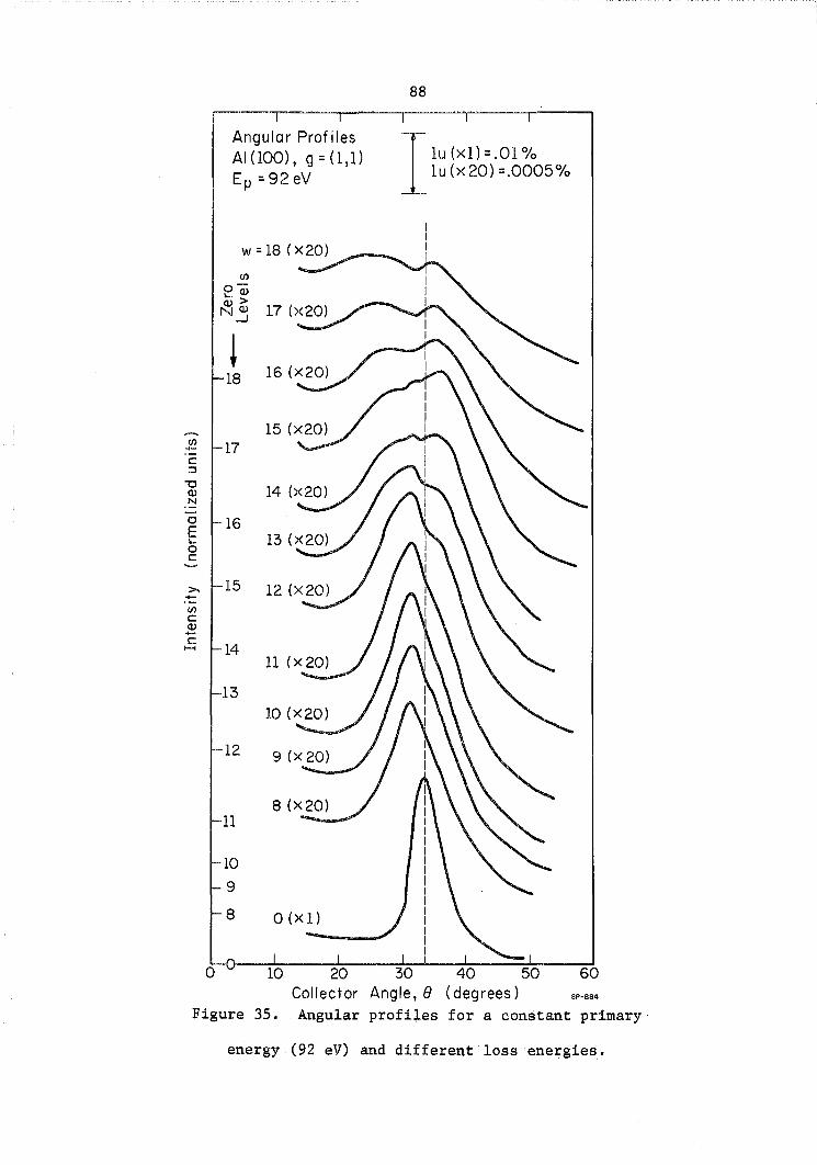
en .,_ c: :::l
""0 <ll N
a E ,_ 0 c:
>. ..,_ en c: <ll ...... c .......
0
Angular Profiles Al(lOO), g=(l,l) Ep =92eV
en o,_<L> <ll> N<ll
.....J
l 18
17
16
15
14
13
-12
Collector
88
I lu (xl) =.01% _ lu (x20) =.0005%
60 SP-884
Figure 35. Angular profiles for a constant primary
energy (92 eV) and different loss energies.

1/) +-c ::J
"0 Q) N
0 E .... 0 c
>. +-1/) c Q) +-c
1-j
89
Angular Profiles Al(lOO), g=(l,l), Ep=96eV
1/)
Q) > ~ 0 .... Q)
N
+ 18
17
16
15
14
13
12
11
10
9
8
10
-r lu (X20) = .0005%
j_
20 30 40 50 60
Collector Angle, 8 (degrees) SP·B62
Figure 36. Angular profiles for a constant primary
energy (96 eV) and different loss energies.

IJ) -c: ::I
"0 (lJ
.~ 0 E .... 0 c:
>. ;!:: rn c: Q) -c: ......
Angular Profiles AI (100), g = ( 1,1), Ep = lOOeV T
w = 19 (><50)
IJ)
Q)
> .3 0 .... Q)
N
~ 19
17
18
16
15
13
12
11
10
9 8
lu (x 20) = .0005% lu(><50)=.0002%
_L
0 0--~----~~--~~--~~--~~--~
Figure 37. Angular profiles for a constant primary energy
(100 eV) and different loss energies.

91
For instance, if we examine Figure 35, we can observe the surface
plasmon peak beginning at 10 eV move to slightly lower angles as we increase
the loss energy to 13 eV. As we increase the loss energy to 17 eV the surface
plasmon peak moves out more rapidly to lower angles, a consequence of the
increasing plasmon wavevector. But at the same time we can see another peak
just to the low angle side of the elastic peak grow for w = 14 and 15 eV. This
peak, together with the peak on the high angle side is a bulk plasmon peak.
This same effect is seen in Figure 36. In Figure 37, E = 100 eV, the strength p
of the surface plasmon peak decreases rapidly, and is about gone for w = 14 eV.
Above w = 14 eV, the bulk plasmon peaks are much larger (and closer in angle to
the elastic peak) and show a definite doublet at w = 18 and 19 eV due to
sideband diffraction. The conclusion that this structure is due to bul~
plasmon excitation also follows from examining the loss profiles in Figure 27
for E = 100 eV. p
Thus, if we look at Figure 31 again, the doublet for E = 90 and 92 eV p
probably consists of a surface plasmon peak on the low angle side of the elastic
peak and a bulk plasmon on the high angle side. However the doublet at E = 98 p
eV and again at E = 106 eV is undoubtedly a bulk plasmon doublet due to p
sideband diffraction.
In addition to identifying the dynamical origin of various details
in the measured intensities, we also can determine the dispersion relations of
the surface and bulk plasmons from plots such as shown in Figures 35, 36 and 37.
We can do this by either making a straightforward kinematic calculation, using
the law of conservation of momentum parallel to the surface, as done in a

rn +-c: ::l
"'0 Q) N
0 E ._ 0 c:
>. -rn c: Q) ...... c: ,._.
Angular Profiles A I ( 100) I g = ( 1 , 0) w = 10 eV
rn Q)
> ~ 0 .... Q)
N
+ 128 126
124
122
120
118
-116
114
112
110
108
106
92
Ilu (x 50)=.0002% 1u (X 100) =.0001%
Ep=128(X100)
126(X50)
124 (X50)
122 (X50)
120 (x50)
118 (X50)
116 (X 50)
114 (x50)
112 (X 50)
110 (X 50)
108 (X50)
106 (X50)
104_.----~--~----~----~--~----~--~ o ro ~ ~ ~ w oo Collector Angle, 8 (degrees) SP-886
Figure 38. Inelastic angular profiles, w = 10 eV, in the
(10) direction. Each black dot indicates the position
of eEl . for each primary energy. ast~c

(/) +-c:: ::1
"'0 Q) N
c E ...... 0 c::
>. .... (/)
c:: Q) -c:: ......
Angu lor Profiles Al(lOO), g =(1,0) w = 12 eV
(/)
Q) > .5 0 ......
~
+ 130
-128 126
124
122
120
118
·-116
114
112
110
108
-106
0 104 10
93
I lu (X 50)= .0002% . lu(Xl00)=.0001%
128 (X 100)
126 (X 50)
124 (X 50)
122 (x50)
120 (X50)
118 (x50)
116 (x50)
114 (X50)
112 (X 50)·
110 (X 50)
108 (X50)
106 (X50)
80
SP-687
Figure 39. Inelastic angular profiles, w = 12 eV, in the
(10) direction. Each black dot indicates the position
of eEl . for each primary energy. ast1.c

IJ) -c: ::J
"0 Q) N
c E .... 0 c:
>. ..... IJ)
c: Q) ..... c:
1-1
0
Angular Profiles Al(lOO) I g=(l,O) w = 14eV
IJ)
Q)
> ~ 0 .... Q)
N
~ 128 126
124
122
116
114
112
110
108
106
104
94
I lu(x 50) =.0002% lu( x 100) =.0001%
126 (X50)
124 (X50)
122 (X50)
120 (X50)
118 (X50)
116 (X50)
114 (X 50)
112 (X 50)
110 (x50)
108 (X 50)
106 (X50) 104 (X50)
80
SP-888
Figure 40. Inelastic angular profiles, w = 14 eV, in the
(10) direction. Each black dot indicates the position
of 8Elastic for each primary energy.

(/) -c: ;:,
"0 Q.) N
0 E ..... 0 c:
>-..... (/)
c: Q.) ...... c: ......
Angular Profiles Al(lOO), g=(l,O) w = l6eV
(/)
Q.)
> ~ 0 ..... Q.)
N
~ 130
-128 -126
124
122
118
116
114
112
110
106
I lu(X50) = .0002% lu(XlOO) =.0001%
Ep=130(X100)
128(X100)
126 (X 50)
124 (X 50)
122 (X 50)
120 (X 50)
118 (X 50)
116 (X 50)
114 (X 50)
112 (X50)
110(X50)
108 (X 50)
106 (X 50)
Figure 41.
(10) direction. Each black dot indicates the
position of eEl t' for each primary energy. as 1.c
the

96
preceeding paragraph, or we can use a quantum field theoretical treatment as
done by Duke and Bagchi. 36 The QFT treatment should yield a more accurate
dispersion relation, because it takes account of the various dynamical scattering
factors present. We refer the interested reader to reference 36 for details of
the calculation.
Finally, we will include the next four figures for comparative
purposes only. Figures 38 to 41 show a series of angular profiles in the (10)
plane for energy losses w = 10, 12, 14 and 16 eV taken over a range of primary
energies which includes the (10) Bragg peak at 107 eV. We should note the
inelastic electrons are partially diffracted into beams and that these diffraction
peaks move from the low angle side of the elastic peak to the high angle side
as the incident energy increases above the Bragg energy. However~ there is a
definite lack of substructure present. This could be due to two things. First~
the absolute tntensity of the beams is lower in this diffraction direction by a
factor between 2.5 and 5. This then might hide some of the structure. Second 9
the surface and bulk plasmon loss peaks in this diffraction direction have a
smaller half-width than in other directions. Thus, at loss energies at which
the excitation should have a large wavevector and hence produce an observable
angular splitting, the excitation strength is greatly reduced.

97
3.5 Comparison of Experimental and Theoretical Profiles
In this section, we briefly will compare some of our experimental
profiles with some theoretical profiles calculated by Duke and Bagchi 36 ~ 37
72 73 and by Laramore and Duke. '
The profiles for both elastic and inelastic intensities calculated by
Duke and Bagchi are shown in Figures 42-48 together with the corresponding
experimental profiles. The elastic profiles calculated by Laramore and Duke
are shown in Figure 49. There are significant differences in the models used
in these two sets of theoretical calculations. Laramore and Duke used a finite
33 34 . temperature version of the inelastic collision model ' w~th an electron-ion-
core potential described by s, p, and d partial wave phase shifts to describe
the elastic scattering from the solid. Bagchi and Duke, on the other hand~
used a isotropic scattering version (s-wave scattering only) of the inelastic
collision model which was also temperature independent in order to calculate a
series of inelastic profiles. The less complete latter model was used for the
talculations in order to place reasonable limits on the computation time of the
profiles. However, these profiles are expected to give qualitative fits of the
lineshapes and peak positions of the experimental profiles. Further calculations
75 indicate that multiple-scattering phenomena can introduce additional structure
into the profiles, but that the "kinematic" effects persist~ i.e., they are
merely augmented by the dynamical effects.
Figures 42 and 43 show a set of experimental and theoretical energy
profiles for loss energies w = 0, 10, 14 and 16 eV. The theoretical profiles are
those of Duke and Bagchi. The vertical axis of the experimental profiles is in
units of percent reflectivity, while that of the theoretical profiles is in cross
section units of square angstroms.

......... 0
-1--1
~?fl. .003 - .......... >->. --.;:;; . u;
~ ~.002 -c c 1--1 1--1
0 0 (.)-
:;: ~ .001 ~ E 0·Q) ~
..c:.Q)
98
Energy Profiles AI (100) g=(ll) w = 10 eV
--- Experi menta I -Theory
~--~ w 06_0 _____ 7~0-----8~0-----9~0-----10~0----l-l~0-----120
-0 - 1--1
Energy Profiles AI ( 100) g=(ll)
~?fl. .08 w=O .._..._..
- 0 o_ .5:2 c - Q) ~ E o·Q) ~
..c:.Q)
~--~ w
.06
.02
1\
I ' I \ I \ I \ I \ I \ I \ I \
I \ I \
I \ , \ , ' ,"' '\ ,, ' ~~ '
'
Experimental Theory
' ', 0 ~----~----~~----~----~--~~~----~ 60 70 80 90 100
Primary Energy (eV) 110 120
SP-964
Figure 42. Theoretical and experimental energy intensity
profiles in the (11) diffraction direction~

-.......... 0 (\J 1-1
<(~ .._0 -Z">-·--(/) ·-c (/) (]) c - (]) c-+-
1-1 c 1--1
0- .0008 u-8
:;:: c (]) (]) o E (]) ·-
..c ~ .0004 1-o.
>< w
-0 ......... 1--1
~~ -->- >---·u; ·u; c c (]) (]) --c c
I-I 1--1
0 0 u-+-·- c - (]) ~ E 0·-(]) !.....
..c (]) ~-~
w
.002
.001
0 60
I I
70
I I
I I I
I I
I I
I
99
,'\ I \ I ' I ' I \ I
I \ I ' I ' I I
I D I I I
I ' I '
Energy Profiles AI ( 100) g = (11) w = 16eV
Energy Profiles AI (100) g = (11) w = 14eV
/' I \ I \ I \
I \ I ... , \ \ \ \ \ \ \ \ \ \ \ \ \ \
'
Primary Energy 120
SP-962
Figure 43. Theoretical and experimental energy intensity
profiles in the (11) diffraction direction.

100
The theoretical inelastic profiles seen in these two figures were
calculated using the dispersion relations of the plasmons previously determined36
and the parameters used in the calculation of the elastic profile. Before
proceeding, it should be noted that these inelastic profiles, together with
h f 11 d h bl . h d b D k d B h· 36 th 1 . 1 t• t ose to o ow an t ose pu 1.s e y u e an age 1. , are e on y 1.ne as 1.c
profiles calculated to be compared with experiment. Because of the nature
of the calculations, we can only compare relative intensities of the inelastics
if we normalize the experimental and theoretical elastic peak heights to
unity.
Examining Figures 42 and 43, we see then that the inelastic peak
shapes and positions of the experimental and theoretical profiles agree quite
well. In the worst case, for w = 14 eV, the IE peak differs by only 3 eV
between experiment and theory. The agreement between the relative intensities
of the EI to IE peaks for the different losses is also found to be quite good.
The absolute intensities of the theoretical inelastic (w ~ 0) profiles in
Figures 42 and 43 are too small by a factor of 8. This makes the theoretical
profiles !ar~E. than the experimental profiles (after normalization) by a
factor of less than two. Thus the empirical electron-plasmon vertex used by
Duke and Bagchi does, in fact, give approximately the correct relative
intensities of the elastic and inelastic crosi sections.
Figure 44 shows a series of experimental and theoretical energy
loss profiles, equivalent to the conditions described for Figure 27. As the
primary energy increases above the Bragg energy at 86 eV, the strength of the

-CJ) -
-CJ)
c Q) -c
.........
Experiment ----Theory
Bt=BE-2.5°
" Ep I,, I \
100 I \ eV I \ ~ 100 1\
I \
l' ' 95 I \
11; 95 I\ I
I \ I I v
I I I I
85 / I
85
101
""''"' ' ' I \ I \
!Jf;:_ r I \
/ \ I \J I I I
I
A
Bt =BE+ 2.5° " " I \
I \ I ' I \
I \
:M " '\ ' \ ' ' I \
I \
!)A ,...,"' I \ I \ I \ I \
/ "
~------~~~~~--~~~~~--~~~~0 20 10 0 20 0
Energy Loss ( eV)
CJ)
Q)
> Q)
_J
0 ~
~
~ lOO{T)
lOO{E)
95{T)
95(E)
85{E) 85{T)
SP-961
Figure 44. Theoretical and experimental energy loss
profiles in the (11) diffraction direction.

102
bulk plasmon loss peak grows relative to that of the surface plasmon. This is
seen in both the experimental and theoretical curves. Differences in relative
intensities of the two losses can be explained by remembering that the
experimental profiles contain the electrons which have scattered both
coherently and incoherently from the solid.
Finally we will compare some theoretical and experimental angular
profiles. Figures 45 and 46 show a series of angular profiles in the (11)
diffraction direction for different loss energies and with two different primary
e.nergies - EB and E + 10 eV. · The theoretical profiles in Figure 45 ragg · Bragg
clearly shows the surface plasmon doublet for w = 10 eV and demonstrates that
these peaks move apart for larger w (and hence larger momentum). For
w = 14 eV, the profile shows a small bulk plasmon peak near eElastic and just
the remains of the large angle surface plasmon. For w 16 and 18 eV, the
theoretical profile only shows a surface plasmon peak on the low angle side
of eEl . • The experimental profiles agree fairly well, with the absence astl.c
of the surface plasmon doublet being explained by our finite angular resolution.
The major discrepancy is in the additional peak on the high angle side of
e for w = 16 and 18 eV. Elastic This is apparently a bulk plasmon loss, with
a larger intensity than predicted by the theory. Figure 46 is similar to
Figure 45, except that the surface plasmon doublet is seen experimentally for
w = 12 eV, and thew= 14 profile shows the surface and bulk plasmon peaks seen
in the theory. The systematic error in eEl . between the experimental and aStl.C
theoretical profiles will be discussed at the end of this section.

-18. CJ)
."!:: 16 c :J
>. !o-e .....
..c
-CJ)
c (]) ..... c
1-1
10 8
0
Theory Ep=86eV
103
Experiment
0~ ~o-Q) (])> NQ)
_J
l 18, 16
14
12
10
8
SP-950
Figure 45. Theoretical and experimental inelastic angular
profiles in the (11) diffraction direction for a
primary energy of 86 eV.

-c ~
~ 16 '-0 '--..0
-en c Q) -c
1-t
0
104
Theory Experiment E p = 96 eV
10
-:JV\:_8
en ot-Q) Q)> Nj
~ 18
16
14
12
10 8
SP-951
Figure 46. Theoretical and experimental inelastic angular
profiles in the (11) diffraction direction for a
primary energy of 96 eV.

105
Figure 47 shows a series of w = 16 eV angular profiles for different
primary energies on either side of the (11) Bragg energy at 86 eV. The
experimental profiles are in adequate agreement with the theoretical profiles.
We can follow the low angle surface plasmon peak and watch it disappear as a
function of primary energy. At the same time, the theory shows a bulk plasmon
peak beginning to grow forE 94 eV, and eventually shifting to the high p
angle side of eEl . for larger primary energy. This is seen in the ast1.c
experiment, although the bulk plasmon begins to appear near E = 90 eV with p
a strength greater than in the theory. We can also see the sideband diffraction
splitting for E p
106 eV in both the theoretical and experimental profiles,
Finally, Figure 48 shows a set of theoretical and experimental angular
profiles for w ~ 14 eV. The theoretical profiles were calculated with a set
of parameters for illustrative purposes only. The theoretical profiles show
the two surface plasmon peaks on the very low and very high angle sides of
eE.l .• together with a bulk plasmon loss. The bulk plasmon is first seen ast1.c
as a singlet on the low angle side of eEl t' at E = 84 eV, after which it as 1.c p
becomes a doublet about e forE = 88 and 90 eV. For larger values of Elastic p
E , the peak gradually becomes a single peak located on the high angle side p
of eEl i . This is the behavior we see in the experimental profiles (also ast c
refer back to Figures 33 and 34). As was pointed out in Figure 34, we clearly
see the low angle surface plasmon and the two bulk plasmon peaks due to
sideband diffraction at E. = 90 eV, together with the motion of the peak across p
8Elastic.

106
1 ,--,--,--r---,--,---r Angular Profiles,
Ep" 108 {X20) AI (100), g= (1,1), w=16 eV V> Theory
IJ) oGi a; '-> > <IJ<IJ
.5 N_i t
0 108 ... Q)
N
+ 106 106 108
104 104
106
102 102
~ ~ 104 100 100 2 ·c: ·c: ::>
"C ::J
"' '0 .!::! 98 98 Q) 102 0
.!::! E 0 a E c 96 ..... 96 0 c 100 ~
'iii 94 c ~ "' 94
98 c 'iii ...... c ~ 92 c 96 92 >-I
94 90 90
92
88 88
86 86
84 84
90 82 88
82 70 86 0 Collector Angle I e (degrees)
84 SP-963
I 0 50
Collector Angle, 8 (degrees) SP-886
Figure 47. Theoretical and experimental inelastic angular
profiles in the (11) diffraction direction for a loss
energy of 16 eV.

-(/) -+-
c: :::::3
'"'0 Q) N
0 E lo.-0 c: ->. -(/)
c: Q) -c:
1--1
107
Theory w = 14 eV nw5 ( p11 ) = 8.1 + 4.0p 11 + 6.0 p 1~ nwb(p) =13.3 + 3.048p2
Ep (X 20) ----- ~02 (xlO)- 102 --1'-t- eV
Zero Levels
~1~~ __)~90
Experiment w = 14eV
' •" Ep ...... / \ -\
\ /'' \. 102 '-" \ - eV , ... , \
I \ \ '~1 \ '-100
\ \
' ' .... 98
~90
~88 _./\ "- 86 . I" 84
40 80 (degrees)
Figure 48. Theoretical and experimental inelastic
angular profiles in the (11) diffraction
direction for a loss energy of 14 eV.
SS-919

108
There is a systematic error of 3° to 6° between the theoretical and
experimental values of A.... in some of the angular profiles. As outlined vt:lastic
in detail in reference 4, there are at least 16 sources of alignment error,
nine of which are angular errors. Some of these, such as the alignment of the
electron beam direction and the alignment of the crystal lattice planes with the
target axis of rotation affect the real positions of the diffracted electron
beam in space. Other errors, such as due to the uncertainty in the zero position
of the collector affect the value in scattered angle which we assign to the
detected beam. Each alignment is no better than .5°-1° accurate. Thus, we
displayed all the experimental angles as values of the collector angle. While
the absolute value may be in doubt by a few degrees, relative positions are
accurate to within one-half a degree.
Finally, we can compare the shapes and absolute intensities of the
experimental and theoretical elastic energy profiles because in the case of
elastic diffraction, accurate microscopic calculations of these profiles have
. 72 73 been carn.ed out. ) The theoretical profiles, as shown in Figure 49, were
calculated by Laramore and Duke using the model described previously. The
experimental profiles are seen in Figures 22 and 23.
The theoretical and measured line shapes of both the (10) and (11)
beams agree well. The major peaks are in about the same places (refer to
Table 1) and the secondary structure also is reproduced, See, e.g., the
multiple scattering peak at about 62 eV in the (11) profile. The profiles
differ in that the experimental peaks are about half as wide as the theoretical
peaks.

-0 0.50 I-f
~ 0
........ 0.25
0 (.) -Q) lo-0 Q)
~ 0.04
0.01
109
Primary Energy
Energy Profile w= OeV g=(10) V1 = 16.7eV AI ( 100)
Energy Prof i I e w = 0 eV g = (ll) Vr = 16.7 eV AI ( 100)
Figure 49. Theoretical (s, p, d-wave scattering)
elastic energy intensity profiles.
SP-965

110
The absolute intensities of the calculated and observed peaks are
found to be in quantitative agreement. The absolute intensity of the (11)
Bragg peak at 86 eV was calculated to be .055% I .• The agreement between the 0
other (11) peaks is equally good. The absolute intensity of the (10) Bragg
peak at 54 eV was calculated to be about .090% I and was measured to be .044% I , 0 0
a difference of about a factor of 2. This excellent agreement cannot be fully
appreciated until one realizes that the next best calculation for Al, one by
Hoffstein and Baudreaux74 based on a band-structure matching formalism, predicts
a reflected intensity of about 20% I for the (11) Bragg peak at 86 eV, a 0
difference of about a factor of 80 with experiment.
The differences between the calculations of Laramore and Duke and
our experimental measurements of the intensities of the (10) Bragg peaks can
probably be explained by assuming a larger misalignment in this direction than
in the (11) direction. This can come about as a consequence of rotating the
target to bring the (10) diffraction plane into the plane of the collector
rotation (see reference 4 for details). In general, the agreement between the
calculated and observed intensities is surprisingly good with regard to the
absolute magnitude as well as the line shape of both the elastic and inelastic
intensities. Although the models used in the calculations are simplified, they
seem to describe the scattering phenomena quite adequately.

111
4. SUMMARY OF RESULTS AND CONCLUSIONS
The data presented in the last chapter clearly demonstrated the
existence of inelastic low energy electron diffraction. At the same time, the
two-step model of ILEED was verified, as we reported for the first time two clear
peaks in the inelastic energy intensity profiles representing EI and IE
diffraction, and measured systematic correlations between the elastic and
inelastic angular profiles based upon this model
Examining the inelastic profiles in detail, we established the
dependence of inelastic diffraction on different diffraction conditions. The
energy loss profiles demonstrated a new behavior in the change in the relative
heights of the surface and bulk plasmon losses as the primary energy is swept
across a Bragg energy. This may lend itself as a new test in distinguishing
between the two types of losses in materials where the losses are not clearly
known. We also observed the predicted doublet structure in the surface
plasmon angular profiles which is due to the localization of the excitation
momentum along the surface. We reported for the first time the experimental
observation of sideband diffraction for a bulk plasmon excitation. We observed
the predicted sideband diffraction in the inelastic angular profile and possibly
in the inelastic energy profile.
The energy loss profiles indicate the occurance of some low energy
losses whose presence is detected only under certain energy and momentum
conditions. A high resolution energy-angular instrument probably would yield
information on the nature of these losses.

112
Finally, we briefly demonstrated that ILEED is sensitive to
surface conditions. The experimental profiles, when coupled with a complete
theory of inelastic diffraction, yield36 an adequate description of the plasmon
dispersion relations, coupling relations, damping parameters, etc., thus
increasing our knowledge of the chemical and electronic properties of solid
surfaces.

113
REFERENCES
1. P. P. Reichertz and H. E. Farnsworth, Phys. Rev. 11, 1902 (1949).
2. J. 0. Porteus, in The Structure and Chemistry of Solid Surfaces, edited by G. A. Somorjai (Wiley, N.Y., 1969) p. 12-1.
3. M.P. Seah, Surface Science ll• 132 (1969).
4. T. L. Cooper, Ph.D. thesis, University of Illinois, 1970; (to be published).
5. T. L. Cooper, J. M. Burkstrand and F. M. Propst, Program of the Thirtieth Annual Conference on Physical Electronics, 1970 (unpublished).
6. C. Davisson and L. H. Germer, Phys. Rev. 30, 705 (1927).
7. J. W. May, Ind. Eng. Chern. 22, 18 (1965).
8. J. J. Lander, Prog. Solid State Chern. ~' 26 (1965).
9. P. J. Estrup and E. G. McRae, Surface Science ~' 1 (1971).
10. E. J. Scheibner and L. N. Tharp, Surface Science ~' 247 (1967).
11. K. G. McKay, Adv.in Electron. and Electron Physics !• 65 (1948).
12. 0. Hachenberg and W. Brauer, Adv. in Electron. and Electron Physics 11, 413 (1959) 0
13. A. J. Dekker, SoHd Statt? Physics _(, 251 (1958),
14. L. Marton, et. al., Adv. in Electron. and Electron Ph~sics z, 183 (1955).
15. 0. Klemperer and J. P. Shepherd, Adv. Physics 12, 355 (1963).
16. H. Raether, in Springer Tracts in Modern Physics 38, 84 (Springer-Verlag, Berlin, 1965).
17. R. H. Ritchie, Phys. Rev. 106, 874 (1957).
18. w. A. Harrison, Solid State Theory (McGraw-Hill, N. y. ' 1970).
19. c. Powell and J. Swan, Phys. Rev. 115, 869 (1959).
20. c. Powell and J. Swan, Phys. Rev. 118, 640 (1960).

114
21. E. Stern and R. Ferrell, Phys. Rev. 120, 130 (1960),
22. J. Swan, A. Otto and H. Gellenzer, Phys. Stat. Sol. ~. 171 (1967).
23. M. Williams, E. Arakawa and 1. Emerson, Surface Science.§_, 127 (1967).
24. J. C. Turnbull and H. E. Farnsworth, Phys. Rev.~. 507 (1938).
25. W. H. Weber and M. B. Webb, Phys. Rev. 177, 1103 (1969).
26. M. P. Seah, Surface Science 12• 161 (1969).
27. E. Bauer, Z. Physik 224, 19 (1969).
28. J. I. Gersten, Phys. Rev. 188, 774 (1969).
29. Y. H. Ohtsuki, J. Phys. Soc. Japan~. 398 (1970).
30. C. B. Duke, G. E. Laramore, and V. Metze, Solid State Commun. ~. 1189 (1970).
31. c. B. Duke and G. E. Laramore, Phys. Rev. B 1_, 3183 (1971).
32. G. E. Laramore and C. B. Duke, Phys. Rev. B 1_, 3198 (1971).
33. c. B. Duke and c. w. Tucker, Jr.' Surface Science 15, 231 (1969).
34. c. B. Duke, J. R. Anderson and C. w. Tucker, Jr.' Surface Science 19' 117 (1970).
· ·35. C. B. Duke, A. J. Howsmon and G. E. Laramore, J. Vac. Sci. Techriol. ~. 10 (1971).
36. C. B. Duke and A. Bagchi, Program of the 1971 International Conference on Solid Surfaces, (submitted to J. Vac. Sci. Technol. for publication in the Mar. 1972 issue).
37. R. W. James, The Optical Principles of the Diffraciton of X-Rays (Bell, London, 1962).
38. C. Kittel, Introduction to Solid State Physics, 3rd Edition (Wiley, N.Y., 1966).
39. E. G. McRae, J. Chem. Phys. 45, 3258 (1966).
40. L. H. Khan, J. P. Hobson and R. A. Armstrong, Phys. Rev. 129, 1513 (1963).

115
41. P. J; Es trup and J. Anderson, Surface Science ~' 101 (196 7) •
42. N. J. Taylor, Surface Science i, 161 (1966).
43. R. L. Gerlach and T. N. Rhodin, Surface Science ~. 1 (1967).
44. E. G. McRae and c. w. Caldwell, Surface Science ]_, 41 (1967).
45. s. Friedman and R. M. Stern, Surface Science Q, 214 (1969).
46. S. Andersson, Surface Science 19, 21 (1970).
47. E. G. McRae and P. J. Jennings, Surface Science 15, 345 (1969).
48. F. Jona, IBM J. Res. Develop. 14, 444 (1970).
49. Ch. Heger and D. Wagner, Z. Phys. 244, 499 (1971).
50. D. E. Beck, Phys. Rev. B (to be published).
51. For further references to theoretical work on plasmon dispersion relations, seeR. Fuchs and K. L. Kliewer, Phys. Rev. Bl, 2270 (1971).
52. M. Hansen, Constitution of Binary Alloys, 2nd Edition, p. 85 (McGraw-Hill, N. Y '·' 1958). .
53. Professor Marvin Metzger, Dept. of Met. and Mining, University of Illinois.
54. J. A. Simpson, Rev. Sci. Instr. _g, 1283 (1961).
55. J. J. Lander, Phys. Rev. 91, 1382 (1953).
56. L. B. Leder and J. A. Simpson, Rev. Sci. Instr. ~. 571 (1958).
57. P. w. Palmberg, Appl. Phys. Letters _!1, 183 (1968).
58. F. Jona, J. Phys. Chern. Solids, 28, 2155 (1967).
59. 0. P. Arora and M. Metzger, Trans. Met. Soc. AIME, 236, 1205 (1966).
60. J. B. Marsh, General Electric Technical Information Series, No. 68-C-287 (1968).
61. W. J. Tegart, The Electrolytic and Chemical Polishing of Metals, Chp. 6 (Pergamon Press, N.Y., 1959).
62. H. H. Farrell and G. A. Somorjai, Phys. Rev. 182, 751 (1969).

116
63. C. C. Chang, Surface Science 25, 53 (1971); (contains 9 references to calibrated Auger experiments)-.-
64. R. E. Weber and A. L. Johnson, J. Appl. Phys. 40, 314 (1969).
65. R. E. Weber and w. T. Peria, J. Appl. Phys. ~' 4355 (1967).
66. R. G. Musket and J. Ferrante, J. Vac. Sci. Techno!. ]_, 14 (1970).
67. s. M. Bedair, et. al.' J. Appl. Phys. 12_, 4026 (1968).
68. W. D. Robertson, 1971 International Conference on Solid Surfaces, Boston, Mass.; (private communication).
69. F. Jona, 1971 International Conference on Solid Surfaces, Boston, Mass.
70. D. E. Edwards, Ph.D. thesis, University of Illinois. 1970; (to be published).
71. C. B. Duke and A. Bagchi, (private communication).
72. G. E. Laramore and C. B. Duke, Phys. Rev. B, (to be published).
73. G. E. Laramore and C. B. Duke (private eommunication).
74. V. Hoffstein and D. S. Boudreaux, Phys. Rev. Letters~' 512 (1970).
75. c. B. Duke and U. Landman (private communication).

117
VITA
James Michael Burkstrand was born in Philadelphia, Pennsylvania, on
January 29, 1946. He attended Catholic Central High School in Troy, New York
graduating in 1963. In September, 1963, he enrolled at Rensselaer Polytechnic
Institute in Troy, New York, and in June, 1967, graudated with a B.S. in Physics.
In September, 1967, he began graduate study in Physics at the University of
Illinois. He received his M.S. in Physics in February of 1969. While a
graduate student, he served as a Teaching Assistant in the Physics Department
for one year, and as a Research Assistant in the Coordinated Science Laboratory
and the Physics Department for the remaining time of his graduate education.