UG0574 User Guide RTG4 FPGA Fabric - Microsemi
126
UG0574 User Guide RTG4 FPGA Fabric
Transcript of UG0574 User Guide RTG4 FPGA Fabric - Microsemi

UG0574User Guide
RTG4 FPGA Fabric

50200574. 6.0 3/21
Microsemi HeadquartersOne Enterprise, Aliso Viejo,CA 92656 USAWithin the USA: +1 (800) 713-4113 Outside the USA: +1 (949) 380-6100Sales: +1 (949) 380-6136Fax: +1 (949) 215-4996Email: [email protected]
©2021 Microsemi, a wholly owned subsidiary of Microchip Technology Inc. All rights reserved. Microsemi and the Microsemi logo are registered trademarks of Microsemi Corporation. All other trademarks and service marks are the property of their respective owners.
Microsemi makes no warranty, representation, or guarantee regarding the information contained herein or the suitability of its products and services for any particular purpose, nor does Microsemi assume any liability whatsoever arising out of the application or use of any product or circuit. The products sold hereunder and any other products sold by Microsemi have been subject to limited testing and should not be used in conjunction with mission-critical equipment or applications. Any performance specifications are believed to be reliable but are not verified, and Buyer must conduct and complete all performance and other testing of the products, alone and together with, or installed in, any end-products. Buyer shall not rely on any data and performance specifications or parameters provided by Microsemi. It is the Buyer’s responsibility to independently determine suitability of any products and to test and verify the same. The information provided by Microsemi hereunder is provided “as is, where is” and with all faults, and the entire risk associated with such information is entirely with the Buyer. Microsemi does not grant, explicitly or implicitly, to any party any patent rights, licenses, or any other IP rights, whether with regard to such information itself or anything described by such information. Information provided in this document is proprietary to Microsemi, and Microsemi reserves the right to make any changes to the information in this document or to any products and services at any time without notice.
About MicrosemiMicrosemi, a wholly owned subsidiary of Microchip Technology Inc. (Nasdaq: MCHP), offers a comprehensive portfolio of semiconductor and system solutions for aerospace & defense, communications, data center and industrial markets. Products include high-performance and radiation-hardened analog mixed-signal integrated circuits, FPGAs, SoCs and ASICs; power management products; timing and synchronization devices and precise time solutions, setting the world's standard for time; voice processing devices; RF solutions; discrete components; enterprise storage and communication solutions, security technologies and scalable anti-tamper products; Ethernet solutions; Power-over-Ethernet ICs and midspans; as well as custom design capabilities and services. Learn more at www.microsemi.com.

Contents
1 Revision History . . . . . . . . . . . . . . . . . . . . . . . . . . . . . . . . . . . . . . . . . . . . . . . . . . . . . 11.1 Revision 6.0 . . . . . . . . . . . . . . . . . . . . . . . . . . . . . . . . . . . . . . . . . . . . . . . . . . . . . . . . . . . . . . . . . . . . . . . 11.2 Revision 5.0 . . . . . . . . . . . . . . . . . . . . . . . . . . . . . . . . . . . . . . . . . . . . . . . . . . . . . . . . . . . . . . . . . . . . . . . 11.3 Revision 4.0 . . . . . . . . . . . . . . . . . . . . . . . . . . . . . . . . . . . . . . . . . . . . . . . . . . . . . . . . . . . . . . . . . . . . . . . 11.4 Revision 3.0 . . . . . . . . . . . . . . . . . . . . . . . . . . . . . . . . . . . . . . . . . . . . . . . . . . . . . . . . . . . . . . . . . . . . . . . 11.5 Revision 2.0 . . . . . . . . . . . . . . . . . . . . . . . . . . . . . . . . . . . . . . . . . . . . . . . . . . . . . . . . . . . . . . . . . . . . . . . 21.6 Revision 1.0 . . . . . . . . . . . . . . . . . . . . . . . . . . . . . . . . . . . . . . . . . . . . . . . . . . . . . . . . . . . . . . . . . . . . . . . 2
2 Fabric Overview . . . . . . . . . . . . . . . . . . . . . . . . . . . . . . . . . . . . . . . . . . . . . . . . . . . . . 3
3 Logic Elements and Routing . . . . . . . . . . . . . . . . . . . . . . . . . . . . . . . . . . . . . . . . . . . 53.1 Logic Element . . . . . . . . . . . . . . . . . . . . . . . . . . . . . . . . . . . . . . . . . . . . . . . . . . . . . . . . . . . . . . . . . . . . . 5
3.1.1 4-Input LUT with Carry Chain . . . . . . . . . . . . . . . . . . . . . . . . . . . . . . . . . . . . . . . . . . . . . . . . . . 53.1.2 STMR-D Flip-Flop . . . . . . . . . . . . . . . . . . . . . . . . . . . . . . . . . . . . . . . . . . . . . . . . . . . . . . . . . . . 63.1.3 Interface Logic . . . . . . . . . . . . . . . . . . . . . . . . . . . . . . . . . . . . . . . . . . . . . . . . . . . . . . . . . . . . . . 73.1.4 I/O Element . . . . . . . . . . . . . . . . . . . . . . . . . . . . . . . . . . . . . . . . . . . . . . . . . . . . . . . . . . . . . . . . 7
3.2 Logic Cluster . . . . . . . . . . . . . . . . . . . . . . . . . . . . . . . . . . . . . . . . . . . . . . . . . . . . . . . . . . . . . . . . . . . . . . 83.3 Routing Architecture . . . . . . . . . . . . . . . . . . . . . . . . . . . . . . . . . . . . . . . . . . . . . . . . . . . . . . . . . . . . . . . . 93.4 Libero Compile Report - Fabric Resources . . . . . . . . . . . . . . . . . . . . . . . . . . . . . . . . . . . . . . . . . . . . . . 10
4 Embedded Memory Blocks . . . . . . . . . . . . . . . . . . . . . . . . . . . . . . . . . . . . . . . . . . . 114.1 LSRAM . . . . . . . . . . . . . . . . . . . . . . . . . . . . . . . . . . . . . . . . . . . . . . . . . . . . . . . . . . . . . . . . . . . . . . . . . . 12
4.1.1 Dual-Port Mode . . . . . . . . . . . . . . . . . . . . . . . . . . . . . . . . . . . . . . . . . . . . . . . . . . . . . . . . . . . . 144.1.2 Two-Port Mode . . . . . . . . . . . . . . . . . . . . . . . . . . . . . . . . . . . . . . . . . . . . . . . . . . . . . . . . . . . . 154.1.3 LSRAM Read Operation . . . . . . . . . . . . . . . . . . . . . . . . . . . . . . . . . . . . . . . . . . . . . . . . . . . . . 184.1.4 LSRAM Write Operation . . . . . . . . . . . . . . . . . . . . . . . . . . . . . . . . . . . . . . . . . . . . . . . . . . . . . 184.1.5 Pipelined Read Synchronous Reset Operation . . . . . . . . . . . . . . . . . . . . . . . . . . . . . . . . . . . . 204.1.6 Pipelined Read Asynchronous Reset Operation . . . . . . . . . . . . . . . . . . . . . . . . . . . . . . . . . . . 204.1.7 LSRAM ECC . . . . . . . . . . . . . . . . . . . . . . . . . . . . . . . . . . . . . . . . . . . . . . . . . . . . . . . . . . . . . . 214.1.8 Using LSRAM in a Design . . . . . . . . . . . . . . . . . . . . . . . . . . . . . . . . . . . . . . . . . . . . . . . . . . . . 224.1.9 Use Model: LSRAM Write-Feed-Through using Fabric Logic . . . . . . . . . . . . . . . . . . . . . . . . . 494.1.10 Debugging LSRAMs Using SmartDebug . . . . . . . . . . . . . . . . . . . . . . . . . . . . . . . . . . . . . . . . . 51
4.2 µSRAM . . . . . . . . . . . . . . . . . . . . . . . . . . . . . . . . . . . . . . . . . . . . . . . . . . . . . . . . . . . . . . . . . . . . . . . . . . 554.2.1 µSRAM Read Operation . . . . . . . . . . . . . . . . . . . . . . . . . . . . . . . . . . . . . . . . . . . . . . . . . . . . . 564.2.2 µSRAM Write Operation . . . . . . . . . . . . . . . . . . . . . . . . . . . . . . . . . . . . . . . . . . . . . . . . . . . . . 604.2.3 µSRAM Synchronous Reset Operation . . . . . . . . . . . . . . . . . . . . . . . . . . . . . . . . . . . . . . . . . . 614.2.4 µSRAM Asynchronous Reset Operation . . . . . . . . . . . . . . . . . . . . . . . . . . . . . . . . . . . . . . . . . 614.2.5 µSRAM ECC . . . . . . . . . . . . . . . . . . . . . . . . . . . . . . . . . . . . . . . . . . . . . . . . . . . . . . . . . . . . . . 624.2.6 Using µSRAM in a Design . . . . . . . . . . . . . . . . . . . . . . . . . . . . . . . . . . . . . . . . . . . . . . . . . . . . 634.2.7 Collision Behavior . . . . . . . . . . . . . . . . . . . . . . . . . . . . . . . . . . . . . . . . . . . . . . . . . . . . . . . . . . 67
4.3 µPROM . . . . . . . . . . . . . . . . . . . . . . . . . . . . . . . . . . . . . . . . . . . . . . . . . . . . . . . . . . . . . . . . . . . . . . . . . 684.3.1 µPROM Architecture and Address Space . . . . . . . . . . . . . . . . . . . . . . . . . . . . . . . . . . . . . . . . 694.3.2 µPROM Operation . . . . . . . . . . . . . . . . . . . . . . . . . . . . . . . . . . . . . . . . . . . . . . . . . . . . . . . . . . 694.3.3 µPROM Configurator . . . . . . . . . . . . . . . . . . . . . . . . . . . . . . . . . . . . . . . . . . . . . . . . . . . . . . . . 70
5 Math Blocks . . . . . . . . . . . . . . . . . . . . . . . . . . . . . . . . . . . . . . . . . . . . . . . . . . . . . . . 805.1 Introduction . . . . . . . . . . . . . . . . . . . . . . . . . . . . . . . . . . . . . . . . . . . . . . . . . . . . . . . . . . . . . . . . . . . . . . 805.2 Features . . . . . . . . . . . . . . . . . . . . . . . . . . . . . . . . . . . . . . . . . . . . . . . . . . . . . . . . . . . . . . . . . . . . . . . . . 805.3 Math Block Resource Table . . . . . . . . . . . . . . . . . . . . . . . . . . . . . . . . . . . . . . . . . . . . . . . . . . . . . . . . . . 805.4 Architecture Description . . . . . . . . . . . . . . . . . . . . . . . . . . . . . . . . . . . . . . . . . . . . . . . . . . . . . . . . . . . . . 81
Microsemi Proprietary UG0574 Revision 6.0 iii

5.4.1 Multiplier . . . . . . . . . . . . . . . . . . . . . . . . . . . . . . . . . . . . . . . . . . . . . . . . . . . . . . . . . . . . . . . . . 815.4.2 Adder or Subtractor . . . . . . . . . . . . . . . . . . . . . . . . . . . . . . . . . . . . . . . . . . . . . . . . . . . . . . . . . 835.4.3 I/O and Control Registers . . . . . . . . . . . . . . . . . . . . . . . . . . . . . . . . . . . . . . . . . . . . . . . . . . . . 83
5.5 Math Blocks Functional Examples . . . . . . . . . . . . . . . . . . . . . . . . . . . . . . . . . . . . . . . . . . . . . . . . . . . . . 845.5.1 Designing with Math Blocks . . . . . . . . . . . . . . . . . . . . . . . . . . . . . . . . . . . . . . . . . . . . . . . . . . . 845.5.2 Use Models . . . . . . . . . . . . . . . . . . . . . . . . . . . . . . . . . . . . . . . . . . . . . . . . . . . . . . . . . . . . . . . 855.5.3 Coding Style Examples . . . . . . . . . . . . . . . . . . . . . . . . . . . . . . . . . . . . . . . . . . . . . . . . . . . . . . 89
6 Appendix: Supported Memory File Formats . . . . . . . . . . . . . . . . . . . . . . . . . . . . . . 98
7 Appendix: Macro . . . . . . . . . . . . . . . . . . . . . . . . . . . . . . . . . . . . . . . . . . . . . . . . . . 1017.1 LSRAM Macro . . . . . . . . . . . . . . . . . . . . . . . . . . . . . . . . . . . . . . . . . . . . . . . . . . . . . . . . . . . . . . . . . . . 101
7.1.1 A_WIDTH and B_WIDTH . . . . . . . . . . . . . . . . . . . . . . . . . . . . . . . . . . . . . . . . . . . . . . . . . . . 1017.1.2 A_WEN and B_WEN . . . . . . . . . . . . . . . . . . . . . . . . . . . . . . . . . . . . . . . . . . . . . . . . . . . . . . . 1027.1.3 A_ADDR and B_ADDR . . . . . . . . . . . . . . . . . . . . . . . . . . . . . . . . . . . . . . . . . . . . . . . . . . . . . 1027.1.4 A_DIN and B_DIN . . . . . . . . . . . . . . . . . . . . . . . . . . . . . . . . . . . . . . . . . . . . . . . . . . . . . . . . . 1027.1.5 A_DOUT and B_DOUT . . . . . . . . . . . . . . . . . . . . . . . . . . . . . . . . . . . . . . . . . . . . . . . . . . . . . 1037.1.6 A_BLK and B_BLK . . . . . . . . . . . . . . . . . . . . . . . . . . . . . . . . . . . . . . . . . . . . . . . . . . . . . . . . 1037.1.7 A_WMODE and B_WMODE . . . . . . . . . . . . . . . . . . . . . . . . . . . . . . . . . . . . . . . . . . . . . . . . . 1037.1.8 A_CLK and B_CLK . . . . . . . . . . . . . . . . . . . . . . . . . . . . . . . . . . . . . . . . . . . . . . . . . . . . . . . . 1037.1.9 A_REN and B_REN . . . . . . . . . . . . . . . . . . . . . . . . . . . . . . . . . . . . . . . . . . . . . . . . . . . . . . . . 1057.1.10 ARST_N . . . . . . . . . . . . . . . . . . . . . . . . . . . . . . . . . . . . . . . . . . . . . . . . . . . . . . . . . . . . . . . . 1057.1.11 ECC and ECC_DOUT_BYPASS . . . . . . . . . . . . . . . . . . . . . . . . . . . . . . . . . . . . . . . . . . . . . . 1057.1.12 A_SB_CORRECT and B_SB_CORRECT . . . . . . . . . . . . . . . . . . . . . . . . . . . . . . . . . . . . . . . 1057.1.13 A_DB_DETECT and B_DB_DETECT . . . . . . . . . . . . . . . . . . . . . . . . . . . . . . . . . . . . . . . . . . 105
7.2 µSRAM Macro . . . . . . . . . . . . . . . . . . . . . . . . . . . . . . . . . . . . . . . . . . . . . . . . . . . . . . . . . . . . . . . . . . . 1057.2.1 A_WIDTH, B_WIDTH, and C_WIDTH . . . . . . . . . . . . . . . . . . . . . . . . . . . . . . . . . . . . . . . . . . 1067.2.2 C_WEN . . . . . . . . . . . . . . . . . . . . . . . . . . . . . . . . . . . . . . . . . . . . . . . . . . . . . . . . . . . . . . . . . 1067.2.3 A_ADDR, B_ADDR, and C_ADDR . . . . . . . . . . . . . . . . . . . . . . . . . . . . . . . . . . . . . . . . . . . . 1077.2.4 C_DIN . . . . . . . . . . . . . . . . . . . . . . . . . . . . . . . . . . . . . . . . . . . . . . . . . . . . . . . . . . . . . . . . . . 1077.2.5 A_DOUT and B_DOUT . . . . . . . . . . . . . . . . . . . . . . . . . . . . . . . . . . . . . . . . . . . . . . . . . . . . . 1077.2.6 A_BLK, B_BLK, and C_BLK . . . . . . . . . . . . . . . . . . . . . . . . . . . . . . . . . . . . . . . . . . . . . . . . . 1087.2.7 C_CLK . . . . . . . . . . . . . . . . . . . . . . . . . . . . . . . . . . . . . . . . . . . . . . . . . . . . . . . . . . . . . . . . . . 1087.2.8 ARST_N . . . . . . . . . . . . . . . . . . . . . . . . . . . . . . . . . . . . . . . . . . . . . . . . . . . . . . . . . . . . . . . . 1087.2.9 ECC and ECC_DOUT_BYPASS . . . . . . . . . . . . . . . . . . . . . . . . . . . . . . . . . . . . . . . . . . . . . . 1087.2.10 A_SB_CORRECT and B_SB_CORRECT . . . . . . . . . . . . . . . . . . . . . . . . . . . . . . . . . . . . . . . 1087.2.11 A_DB_DETECT and B_DB_DETECT . . . . . . . . . . . . . . . . . . . . . . . . . . . . . . . . . . . . . . . . . . 109
7.3 Math Block Macro . . . . . . . . . . . . . . . . . . . . . . . . . . . . . . . . . . . . . . . . . . . . . . . . . . . . . . . . . . . . . . . . 109
8 Glossary . . . . . . . . . . . . . . . . . . . . . . . . . . . . . . . . . . . . . . . . . . . . . . . . . . . . . . . . 1168.1 Acronyms . . . . . . . . . . . . . . . . . . . . . . . . . . . . . . . . . . . . . . . . . . . . . . . . . . . . . . . . . . . . . . . . . . . . . . . 1168.2 Terminology . . . . . . . . . . . . . . . . . . . . . . . . . . . . . . . . . . . . . . . . . . . . . . . . . . . . . . . . . . . . . . . . . . . . . 118
Microsemi Proprietary UG0574 Revision 6.0 iv

Figures
Figure 1 Functional Block Diagram of RTG4 Family Device . . . . . . . . . . . . . . . . . . . . . . . . . . . . . . . . . . . . . . 3Figure 2 Fabric Layout . . . . . . . . . . . . . . . . . . . . . . . . . . . . . . . . . . . . . . . . . . . . . . . . . . . . . . . . . . . . . . . . . . 4Figure 3 Functional Block Diagram of Logic Element . . . . . . . . . . . . . . . . . . . . . . . . . . . . . . . . . . . . . . . . . . . 5Figure 4 Functional Block Diagram of STMR-D Flip-Flop . . . . . . . . . . . . . . . . . . . . . . . . . . . . . . . . . . . . . . . . 6Figure 5 Functional Block Diagram of Interface Logic . . . . . . . . . . . . . . . . . . . . . . . . . . . . . . . . . . . . . . . . . . 7Figure 6 LSRAM/µSRAM/Math Block Interfacing with ILs in a Row . . . . . . . . . . . . . . . . . . . . . . . . . . . . . . . . 7Figure 7 Functional Block Diagram of I/O Element . . . . . . . . . . . . . . . . . . . . . . . . . . . . . . . . . . . . . . . . . . . . . 8Figure 8 Logic Cluster . . . . . . . . . . . . . . . . . . . . . . . . . . . . . . . . . . . . . . . . . . . . . . . . . . . . . . . . . . . . . . . . . . . 9Figure 9 Sample Compile Report for RT4G150 . . . . . . . . . . . . . . . . . . . . . . . . . . . . . . . . . . . . . . . . . . . . . . 10Figure 10 Functional Block Diagram of LSRAM . . . . . . . . . . . . . . . . . . . . . . . . . . . . . . . . . . . . . . . . . . . . . . . 12Figure 11 Block Select Inputs for Dual-Port Mode . . . . . . . . . . . . . . . . . . . . . . . . . . . . . . . . . . . . . . . . . . . . . 15Figure 12 Two Port Mode x36 Data Flow . . . . . . . . . . . . . . . . . . . . . . . . . . . . . . . . . . . . . . . . . . . . . . . . . . . . 16Figure 13 LSRAM Read Operation . . . . . . . . . . . . . . . . . . . . . . . . . . . . . . . . . . . . . . . . . . . . . . . . . . . . . . . . . 18Figure 14 LSRAM Write Operation— Followed by Earliest Read . . . . . . . . . . . . . . . . . . . . . . . . . . . . . . . . . . 19Figure 15 LSRAM Synchronous Reset Operation . . . . . . . . . . . . . . . . . . . . . . . . . . . . . . . . . . . . . . . . . . . . . 20Figure 16 LSRAM Asynchronous Reset Operation . . . . . . . . . . . . . . . . . . . . . . . . . . . . . . . . . . . . . . . . . . . . 21Figure 17 LSRAM Ports Configured as Dual-Port SRAM - DPSRAM Macro in Libero SoC . . . . . . . . . . . . . . 24Figure 18 Dual-Port Large SRAM Configurator . . . . . . . . . . . . . . . . . . . . . . . . . . . . . . . . . . . . . . . . . . . . . . . 25Figure 19 LSRAM Ports Configured as Two-Port SRAM - TPSRAM Macro in Libero SoC . . . . . . . . . . . . . . 28Figure 20 Two-Port Large SRAM Configurator . . . . . . . . . . . . . . . . . . . . . . . . . . . . . . . . . . . . . . . . . . . . . . . . 29Figure 21 LSRAM Pipelined-ECC BLK Select De-assertion Hold Time Violation After Read . . . . . . . . . . . . 32Figure 22 LSRAM Configurator Fabric Wrapper Logic Mitigating BLK De-assertion Hold Time Issue on Depth
Cascaded LSRAM Component 33Figure 23 DPSRAM_DOUTnopipe_1Kx18_ECCnopipe . . . . . . . . . . . . . . . . . . . . . . . . . . . . . . . . . . . . . . . . . 36Figure 24 DPSRAM_DOUTnopipe_1Kx18_ECCpipe . . . . . . . . . . . . . . . . . . . . . . . . . . . . . . . . . . . . . . . . . . . 36Figure 25 DPSRAM_DOUTpipe_1Kx18_ECCnopipe . . . . . . . . . . . . . . . . . . . . . . . . . . . . . . . . . . . . . . . . . . . 37Figure 26 DPSRAM_DOUTpipe_1Kx18_ECCpipe . . . . . . . . . . . . . . . . . . . . . . . . . . . . . . . . . . . . . . . . . . . . . 37Figure 27 DPSRAM_DOUTpipe_HS_1Kx36_noECC . . . . . . . . . . . . . . . . . . . . . . . . . . . . . . . . . . . . . . . . . . . 38Figure 28 DPSRAM_DOUTpipe_LP_2Kx18_noECC . . . . . . . . . . . . . . . . . . . . . . . . . . . . . . . . . . . . . . . . . . . 38Figure 29 TPSRAM_DOUTnopipe_512x36_ECCnopipe . . . . . . . . . . . . . . . . . . . . . . . . . . . . . . . . . . . . . . . . 39Figure 30 TPSRAM_DOUTnopipe_512x36_ECCpipe . . . . . . . . . . . . . . . . . . . . . . . . . . . . . . . . . . . . . . . . . . 39Figure 31 TPSRAM_DOUTpipe_512x36_ECCnopipe . . . . . . . . . . . . . . . . . . . . . . . . . . . . . . . . . . . . . . . . . . 40Figure 32 TPSRAM_DOUTpipe_512x36_ECCpipe . . . . . . . . . . . . . . . . . . . . . . . . . . . . . . . . . . . . . . . . . . . . 40Figure 33 TPSRAM_DOUTpipe_HS_512x72_noECC . . . . . . . . . . . . . . . . . . . . . . . . . . . . . . . . . . . . . . . . . . 41Figure 34 TPSRAM_DOUTpipe_LP_1Kx36_noECC . . . . . . . . . . . . . . . . . . . . . . . . . . . . . . . . . . . . . . . . . . . 41Figure 35 Case A: LSRAM Configurator Component with Comb Delay Gating ECC Flag Outputs, non-Pipelined
ECC 43Figure 36 Case B: LSRAM Read Operation, Pipelined Read without ECC . . . . . . . . . . . . . . . . . . . . . . . . . . 44Figure 37 Case C: Depth Cascaded Dual Port LSRAM Component, Pipelined Read without ECC . . . . . . . . 44Figure 38 Case D: Depth Cascaded Two Port LSRAM Component, Pipelined Read without ECC . . . . . . . . 45Figure 39 Case E: Dual Port LSRAM with Pipelined ECC . . . . . . . . . . . . . . . . . . . . . . . . . . . . . . . . . . . . . . . 46Figure 40 Case F: Two Port LSRAM with Pipelined ECC . . . . . . . . . . . . . . . . . . . . . . . . . . . . . . . . . . . . . . . . 47Figure 41 Libero Project Settings . . . . . . . . . . . . . . . . . . . . . . . . . . . . . . . . . . . . . . . . . . . . . . . . . . . . . . . . . . 48Figure 42 TPSRAM: 0.5 Error Probability and 0.5 Correction Probability . . . . . . . . . . . . . . . . . . . . . . . . . . . . 48Figure 43 TPSRAM: 0.25 Error Probability and 0.85 Correction Probability . . . . . . . . . . . . . . . . . . . . . . . . . . 49Figure 44 TPSRAM: 0.15 Error Probability and 0.15 Correction Probability . . . . . . . . . . . . . . . . . . . . . . . . . . 49Figure 45 Sample Write-Feed-Thorough Fabric Logic . . . . . . . . . . . . . . . . . . . . . . . . . . . . . . . . . . . . . . . . . . 49Figure 46 Write-Feed-Through using Fabric Logic - RTL Schematic View . . . . . . . . . . . . . . . . . . . . . . . . . . . 50Figure 47 Post-Compile Netlist View of active_probe_latch . . . . . . . . . . . . . . . . . . . . . . . . . . . . . . . . . . . . . . 52Figure 48 Instantiation of probeWrite_1 module with PRBWR_IN tied LOW . . . . . . . . . . . . . . . . . . . . . . . . . 52Figure 49 Writing a Logic-1 to the active_probe_latch Handshake Signal . . . . . . . . . . . . . . . . . . . . . . . . . . . 54Figure 50 Functional Block Diagram of µSRAM . . . . . . . . . . . . . . . . . . . . . . . . . . . . . . . . . . . . . . . . . . . . . . . 55Figure 51 Synchronous-Asynchronous Read Operation without Pipeline Registers . . . . . . . . . . . . . . . . . . . 57Figure 52 Synchronous-Synchronous Read Operation with Pipeline Registers . . . . . . . . . . . . . . . . . . . . . . . 58
Microsemi Proprietary UG0574 Revision 6.0 v

Figure 53 Asynchronous Read Operation without Pipeline Registers Waveform . . . . . . . . . . . . . . . . . . . . . . 59Figure 54 Asynchronous Read Operation with Pipeline Registers Waveform . . . . . . . . . . . . . . . . . . . . . . . . 60Figure 55 µSRAM Write Operation . . . . . . . . . . . . . . . . . . . . . . . . . . . . . . . . . . . . . . . . . . . . . . . . . . . . . . . . . 60Figure 56 µSRAM Synchronous Reset Operation . . . . . . . . . . . . . . . . . . . . . . . . . . . . . . . . . . . . . . . . . . . . . 61Figure 57 µSRAM Asynchronous Reset Operation . . . . . . . . . . . . . . . . . . . . . . . . . . . . . . . . . . . . . . . . . . . . 62Figure 58 µSRAM Configurator in Libero SoC . . . . . . . . . . . . . . . . . . . . . . . . . . . . . . . . . . . . . . . . . . . . . . . . 64Figure 59 µSRAM Configurator . . . . . . . . . . . . . . . . . . . . . . . . . . . . . . . . . . . . . . . . . . . . . . . . . . . . . . . . . . . . 64Figure 60 Functional Block Diagram of µPROM . . . . . . . . . . . . . . . . . . . . . . . . . . . . . . . . . . . . . . . . . . . . . . . 68Figure 61 µPROM Memory Blocks . . . . . . . . . . . . . . . . . . . . . . . . . . . . . . . . . . . . . . . . . . . . . . . . . . . . . . . . . 69Figure 62 µPROM Read Operation . . . . . . . . . . . . . . . . . . . . . . . . . . . . . . . . . . . . . . . . . . . . . . . . . . . . . . . . . 69Figure 63 µPROM Configurator in Libero SoC . . . . . . . . . . . . . . . . . . . . . . . . . . . . . . . . . . . . . . . . . . . . . . . . 70Figure 64 RTG4 µPROM Core in Catalog . . . . . . . . . . . . . . . . . . . . . . . . . . . . . . . . . . . . . . . . . . . . . . . . . . . 70Figure 65 µPROM Configurator . . . . . . . . . . . . . . . . . . . . . . . . . . . . . . . . . . . . . . . . . . . . . . . . . . . . . . . . . . . 70Figure 66 Add Data Storage Client Dialog Box . . . . . . . . . . . . . . . . . . . . . . . . . . . . . . . . . . . . . . . . . . . . . . . . 71Figure 67 Import Memory File Dialog Box . . . . . . . . . . . . . . . . . . . . . . . . . . . . . . . . . . . . . . . . . . . . . . . . . . . 72Figure 68 Absolute Path of Memory File . . . . . . . . . . . . . . . . . . . . . . . . . . . . . . . . . . . . . . . . . . . . . . . . . . . . . 72Figure 69 Relative Path of Memory File . . . . . . . . . . . . . . . . . . . . . . . . . . . . . . . . . . . . . . . . . . . . . . . . . . . . . 73Figure 70 Location of Memory File to Copy From . . . . . . . . . . . . . . . . . . . . . . . . . . . . . . . . . . . . . . . . . . . . . . 73Figure 71 Project Sub-Folders Hidden from View . . . . . . . . . . . . . . . . . . . . . . . . . . . . . . . . . . . . . . . . . . . . . . 74Figure 72 Microsemi Binary File (*.mem) Example . . . . . . . . . . . . . . . . . . . . . . . . . . . . . . . . . . . . . . . . . . . . . 74Figure 73 Intel-Hex File Selection . . . . . . . . . . . . . . . . . . . . . . . . . . . . . . . . . . . . . . . . . . . . . . . . . . . . . . . . . . 75Figure 74 Motorola-S File Selection . . . . . . . . . . . . . . . . . . . . . . . . . . . . . . . . . . . . . . . . . . . . . . . . . . . . . . . . 75Figure 75 Simple-Hex File Selection . . . . . . . . . . . . . . . . . . . . . . . . . . . . . . . . . . . . . . . . . . . . . . . . . . . . . . . . 75Figure 76 User Clients Added . . . . . . . . . . . . . . . . . . . . . . . . . . . . . . . . . . . . . . . . . . . . . . . . . . . . . . . . . . . . . 76Figure 77 Editing User Clients . . . . . . . . . . . . . . . . . . . . . . . . . . . . . . . . . . . . . . . . . . . . . . . . . . . . . . . . . . . . 77Figure 78 Edit Data Storage Client Dialog Box . . . . . . . . . . . . . . . . . . . . . . . . . . . . . . . . . . . . . . . . . . . . . . . . 77Figure 79 Deleting a Client . . . . . . . . . . . . . . . . . . . . . . . . . . . . . . . . . . . . . . . . . . . . . . . . . . . . . . . . . . . . . . . 78Figure 80 Update µPROM Memory Content . . . . . . . . . . . . . . . . . . . . . . . . . . . . . . . . . . . . . . . . . . . . . . . . . . 78Figure 81 µPROM Update Tool . . . . . . . . . . . . . . . . . . . . . . . . . . . . . . . . . . . . . . . . . . . . . . . . . . . . . . . . . . . 79Figure 82 Edit Data Storage Client Dialog Box . . . . . . . . . . . . . . . . . . . . . . . . . . . . . . . . . . . . . . . . . . . . . . . . 79Figure 83 Functional Block Diagram of Math Block . . . . . . . . . . . . . . . . . . . . . . . . . . . . . . . . . . . . . . . . . . . . 81Figure 84 Functional Block Diagram of Math Block in Normal Mode . . . . . . . . . . . . . . . . . . . . . . . . . . . . . . . 82Figure 85 Functional Block Diagram of Math Block in DOTP Mode . . . . . . . . . . . . . . . . . . . . . . . . . . . . . . . . 82Figure 86 Non-Pipelined 35 × 35 Multiplier . . . . . . . . . . . . . . . . . . . . . . . . . . . . . . . . . . . . . . . . . . . . . . . . . . . 85Figure 87 Pipeline 35 × 35 Multiplier . . . . . . . . . . . . . . . . . . . . . . . . . . . . . . . . . . . . . . . . . . . . . . . . . . . . . . . . 86Figure 88 9-Bit Complex Multiplication Using DOTP Mode . . . . . . . . . . . . . . . . . . . . . . . . . . . . . . . . . . . . . . 87Figure 89 Rounding Using C-Input and CARRYIN . . . . . . . . . . . . . . . . . . . . . . . . . . . . . . . . . . . . . . . . . . . . . 88Figure 90 Rounding and Trimming of the Final Sum . . . . . . . . . . . . . . . . . . . . . . . . . . . . . . . . . . . . . . . . . . . 88Figure 91 Rounding and Trimming of the Final Sum . . . . . . . . . . . . . . . . . . . . . . . . . . . . . . . . . . . . . . . . . . . 89Figure 92 LSRAM Configurator . . . . . . . . . . . . . . . . . . . . . . . . . . . . . . . . . . . . . . . . . . . . . . . . . . . . . . . . . . . 101Figure 93 µSRAM Configurator . . . . . . . . . . . . . . . . . . . . . . . . . . . . . . . . . . . . . . . . . . . . . . . . . . . . . . . . . . . 106Figure 94 Math Block Configurator . . . . . . . . . . . . . . . . . . . . . . . . . . . . . . . . . . . . . . . . . . . . . . . . . . . . . . 109
Microsemi Proprietary UG0574 Revision 6.0 vi

Microsemi Proprietary UG0574 Revision 6.0 vii
Tables
Table 1 Fabric Resources for RTG4 FPGA Devices . . . . . . . . . . . . . . . . . . . . . . . . . . . . . . . . . . . . . . . . . . . 4Table 2 Number of Logic Elements . . . . . . . . . . . . . . . . . . . . . . . . . . . . . . . . . . . . . . . . . . . . . . . . . . . . . . . . 5Table 3 ILs for Embedded Hard IP Blocks . . . . . . . . . . . . . . . . . . . . . . . . . . . . . . . . . . . . . . . . . . . . . . . . . . . 7Table 4 Fabric Array Coordinate Systems . . . . . . . . . . . . . . . . . . . . . . . . . . . . . . . . . . . . . . . . . . . . . . . . . . . 9Table 5 RTG4 LSRAM, µSRAM, and µPROM Features . . . . . . . . . . . . . . . . . . . . . . . . . . . . . . . . . . . . . . . 11Table 6 RTG4 Embedded Memory Resources . . . . . . . . . . . . . . . . . . . . . . . . . . . . . . . . . . . . . . . . . . . . . . 12Table 7 Port List for LSRAM . . . . . . . . . . . . . . . . . . . . . . . . . . . . . . . . . . . . . . . . . . . . . . . . . . . . . . . . . . . . 13Table 8 Data Width Configurations For Dual-port Mode . . . . . . . . . . . . . . . . . . . . . . . . . . . . . . . . . . . . . . . 14Table 9 Block Select Operation . . . . . . . . . . . . . . . . . . . . . . . . . . . . . . . . . . . . . . . . . . . . . . . . . . . . . . . . . . 14Table 10 Dual-Port Byte Write Enables Settings . . . . . . . . . . . . . . . . . . . . . . . . . . . . . . . . . . . . . . . . . . . . . . 15Table 11 Data Width Configurations for Two-Port Mode . . . . . . . . . . . . . . . . . . . . . . . . . . . . . . . . . . . . . . . . 17Table 12 Block Select Operation in Two-Port Mode . . . . . . . . . . . . . . . . . . . . . . . . . . . . . . . . . . . . . . . . . . . 17Table 13 Two-Port Byte Write Enables For x36 Write Width . . . . . . . . . . . . . . . . . . . . . . . . . . . . . . . . . . . . . 17Table 14 ECC Available Mode . . . . . . . . . . . . . . . . . . . . . . . . . . . . . . . . . . . . . . . . . . . . . . . . . . . . . . . . . . . . 21Table 15 LSRAM Error Flag Status . . . . . . . . . . . . . . . . . . . . . . . . . . . . . . . . . . . . . . . . . . . . . . . . . . . . . . . . 22Table 16 Port List for the DPSRAM Configurator . . . . . . . . . . . . . . . . . . . . . . . . . . . . . . . . . . . . . . . . . . . . . 24Table 17 Port List for the TPSRAM Configurator . . . . . . . . . . . . . . . . . . . . . . . . . . . . . . . . . . . . . . . . . . . . . . 28Table 18 LSRAM Configurator Component Timing and Ports . . . . . . . . . . . . . . . . . . . . . . . . . . . . . . . . . . . . 34Table 19 Functional Timing Waveforms . . . . . . . . . . . . . . . . . . . . . . . . . . . . . . . . . . . . . . . . . . . . . . . . . . . . 42Table 20 ECC Errors Flag . . . . . . . . . . . . . . . . . . . . . . . . . . . . . . . . . . . . . . . . . . . . . . . . . . . . . . . . . . . . . . . 47Table 21 Port List for µSRAM . . . . . . . . . . . . . . . . . . . . . . . . . . . . . . . . . . . . . . . . . . . . . . . . . . . . . . . . . . . . 55Table 22 µSRAM Error Flag Status . . . . . . . . . . . . . . . . . . . . . . . . . . . . . . . . . . . . . . . . . . . . . . . . . . . . . . . . 62Table 23 Collision Scenarios . . . . . . . . . . . . . . . . . . . . . . . . . . . . . . . . . . . . . . . . . . . . . . . . . . . . . . . . . . . . . 67Table 24 Port List for the µPROM Configurator . . . . . . . . . . . . . . . . . . . . . . . . . . . . . . . . . . . . . . . . . . . . . . . 68Table 25 Resources for RTG4 Devices . . . . . . . . . . . . . . . . . . . . . . . . . . . . . . . . . . . . . . . . . . . . . . . . . . . . . 80Table 26 Truth Table for Propagating Operand D of the Adder or Accumulator . . . . . . . . . . . . . . . . . . . . . . 84Table 27 Rounding Examples . . . . . . . . . . . . . . . . . . . . . . . . . . . . . . . . . . . . . . . . . . . . . . . . . . . . . . . . . . . . 88Table 28 Depth × Width Mode Selection . . . . . . . . . . . . . . . . . . . . . . . . . . . . . . . . . . . . . . . . . . . . . . . . . . . 101Table 29 Write/Read Operation Select . . . . . . . . . . . . . . . . . . . . . . . . . . . . . . . . . . . . . . . . . . . . . . . . . . . . 102Table 30 Address Bus Used and Unused Bits . . . . . . . . . . . . . . . . . . . . . . . . . . . . . . . . . . . . . . . . . . . . . . . 102Table 31 Data Input Buses Used and Unused Bits . . . . . . . . . . . . . . . . . . . . . . . . . . . . . . . . . . . . . . . . . . . 102Table 32 Data Output Buses Used and Unused Bits . . . . . . . . . . . . . . . . . . . . . . . . . . . . . . . . . . . . . . . . . . 103Table 33 Block-Port Select . . . . . . . . . . . . . . . . . . . . . . . . . . . . . . . . . . . . . . . . . . . . . . . . . . . . . . . . . . . . . 103Table 34 Width/Depth Mode Selection . . . . . . . . . . . . . . . . . . . . . . . . . . . . . . . . . . . . . . . . . . . . . . . . . . . . 106Table 35 Address Buses Used and Unused Bits . . . . . . . . . . . . . . . . . . . . . . . . . . . . . . . . . . . . . . . . . . . . . 107Table 36 Data Input Bus Used and Unused Bits . . . . . . . . . . . . . . . . . . . . . . . . . . . . . . . . . . . . . . . . . . . . . 107Table 37 Data Output Used and Unused Bits . . . . . . . . . . . . . . . . . . . . . . . . . . . . . . . . . . . . . . . . . . . . . . . 107Table 38 Block-Port Select . . . . . . . . . . . . . . . . . . . . . . . . . . . . . . . . . . . . . . . . . . . . . . . . . . . . . . . . . . . . . 108Table 39 Truth Table for A_ADDR, B_ADDR, A_DOUT, and B_DOUT Registers . . . . . . . . . . . . . . . . . . . 108Table 40 Ports List of Math Block Configurator . . . . . . . . . . . . . . . . . . . . . . . . . . . . . . . . . . . . . . . . . . . . . . 110Table 41 Truth Table for Control Registers ARSHFT17, CDSEL, FDBKSEL, and SUB . . . . . . . . . . . . . . . 115Table 42 Truth Table - Data Registers A, B, C, CARRYIN, P, and OVFL_CARRYOUT . . . . . . . . . . . . . . . 115Table 43 Truth Table - Propagating Data to Operand D . . . . . . . . . . . . . . . . . . . . . . . . . . . . . . . . . . . . . . . 115
Revision History
1 Revision History
The revision history describes the changes that were implemented in the document. The changes are listed by revision, starting with the most current publication.
1.1 Revision 6.0The following is a summary of changes in this revision.
• Updated the information about the SB_CORRECT and DB_DETECT flags in LSRAM ECC, page 21.• Removed the note about LSRAMs not being inferred in the ECC mode by the Synthesis tool (RTL
Inference during Synthesis, page 63).• Updated the LSRAM timing diagrams, see Figure 13, page 18 and Functional Timing Waveforms,
page 42.• LSRAM endianness information was added, see LSRAM, page 12.• Added a note to describe the ECC behavior for uncorrectable errors, see LSRAM ECC, page 21.• Updated Two-Port Data Width Configuration, page 17.• Added all supported memory file formats for µPROM client, see Add Clients to System, page 71.
1.2 Revision 5.0The following is a summary of changes in this revision.
• Added information about the LSRAM hold time violation after read during pipelined-ECC mode, see LSRAM Hold Time Violation, page 31.
• Updated the data widths supported by LSRAM in Two-Port Mode, see Table 11, page 17.• Add Collision Behavior, page 67.• Added the x36 data flow of the two port LSRAM, see Figure 12, page 16.• Added Debugging LSRAMs Using SmartDebug, page 51.• Added LSRAM Configurator Component Timing and Ports, page 34.• Added Simulating ECC Errors in LSRAM, page 47.• Removed x36 and x9 read port and write data width support respectively from Table 11, page 17 as
it is not supported now. For more information, see Customer Advisory Notice (CAN18002.3).• Added Two-Port Block Select Operation, page 17.
1.3 Revision 4.0The following is a summary of changes in this revision.
• When clock is at negative edge, the inversion will be absorb into the SLE with out effecting output polarity.
• During ECC pipeline mode, back to back read, write operations are not allowed.• During accumulation, any error caused by a radiation-induced event (SEU/SET) stays in the
accumulator until it is reset or purged.• Read-before Write and Write-feed through modes are not supported.• Updated Figure 14, page 19 and Table 14, page 21.• The following register names are updated:
• A_IN_BYPASS changed to A_ADD_BYPASS• B_IN_BYPASS changed to B_ADD_BYPASS
1.4 Revision 3.0The following is a summary of changes in this revision.
• The I/O section is removed from this user guide and published as a separate user guide. See UG0741: RTG4 FPGA I/O User Guide.
• Removed BUSY signal reference from µPROM, page 68.• Removed LSRAM write feed-through information.• Updated Table 5, page 11 with µPROM data bus width details.• Updated LSRAM ECC, page 21.
Microsemi Proprietary UG0574 Revision 6.0 1

Revision History
• Updated Figure 94, page 109.• Added Using LSRAM in a Design, page 22.• Added Using µSRAM in a Design, page 63.• Added µPROM Configurator, page 70.• Updated LSRAM Read Operation, page 18.• Added Use Model: LSRAM Write-Feed-Through using Fabric Logic, page 49.• Updated Read Enable information in RTG4 Dual-Port LSRAM Configurator, page 23.• Removed RT4G075 device reference from the document.
1.5 Revision 2.0The following is a summary of changes in this revision.
• Updated the document with FTC inputs.• Updated Features section and Table 5-3.• Updated µSRAM ECC, page 62.• Updated Table 6-3.• Updated Table 6-10.• Updated Low Voltage CMOS (LVCMOS) section.• Added Cold Sparing and Dedicated Global I/Os sections.• Updated Programmable Slew Rate Control section.• Added µPROM, page 68.• Replaced GSR_N signal with ARST_N.
1.6 Revision 1.0The first publication of this document.
Microsemi Proprietary UG0574 Revision 6.0 2

Fabric Overview
2 Fabric Overview
RTG4™ FPGAs feature a fourth-generation FPGA fabric with radiation tolerance. Fabric is the programmable logic section of the RTG4 FPGA, which the user configures with VHDL or Verilog. The RTG4 FPGA fabric consists of the following resources:
• Logic element: These are basic building blocks in the RTG4 FPGA.• Embedded memory blocks: These include large SRAM (LSRAM), microSRAM (µSRAM), and
microPROM (µPROM).• Math blocks: These have a built-in multiplier and adder.The Libero® System-on-Chip (SoC) software (or third-party synthesis tools) automatically infers these logic elements, embedded memories, and math blocks from the user’s register transfer level (RTL) code. For more information about the Libero SoC Classic and Enhanced Constraint design flow, see the Libero SoC Classic Constraint Flow User Guide and Libero SoC for Enhanced Constraint Flow(ECF) User Guide.
The following figure is a top-level functional block diagram of the RTG4 FPGA family. The highlighted fabric block is described in this document.
Figure 1 • Functional Block Diagram of RTG4 Family Device
FPGA FabricUp to 150K Logic Elements
μPROM
16 SpaceWire Clock
and Data Recovery Circuits
Multi-Standard GPIO(1.2 – 3.3 V, LVTTL, LVCMOS, LVDS, HSTL/SSTL, PCI)
Math Blocks(18x18)
PCI Expressx1,x2,x4
2 Per DeviceXAUIXGXS
Native SerDesEPCS
Math Blocks(18x18)
462
Micro SRAM(64x18)
Micro SRAM(64x18)
210
Large SRAM(1024x18)
Large SRAM(1024x18)
209
PORGenerator
JTAG
System
Controller
RT PLLs
24 Lanes Multi Protocol 3.125G SERDES
AXI/AHB
AXI/AHB, XGMII, Direct 20-bit Bus
667 Mb/s DDRController/PHY
AXI/AHB 667 Mb/s DDRController/PHY
Standard Cell /SEL ImmuneFlash Based / SEL Immune
PMA PMA PMA PMA
RC OSC
Microsemi Proprietary UG0574 Revision 6.0 3
Fabric Overview
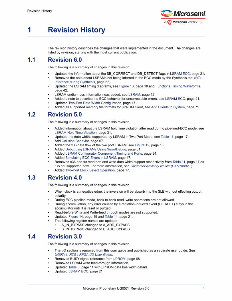
The following figure shows the fabric layout. The FPGA logic resources are displayed as logic clusters (LC). Each LC consists of 12 logic elements (LE). The embedded memory blocks and math blocks are arranged in rows.
Figure 2 • Fabric Layout
The following table lists the available fabric resources in the RTG4 family devices.
Table 1 • Fabric Resources for RTG4 FPGA Devices1
1. 1 Kb = 1024 bits, 1 Mb = 1024 Kb.
Resources RT4G150Logic elements 120,108
Interface logic 31,716
Total logic elements 151,824
LSRAM blocks (24.5-Kb each) 209
Total LSRAM bits (Mb) 5
µSRAM blocks (1.5-Kb each) 210
Total µSRAM bits (Kb) 315
Total RAM (Mb) 5.3
Math blocks (18 × 18 MACC) 462
µPROM (Bits) 374,400
Math Blocks
LSRAMs
μSRAM
μPROM
SerDes and Hardened IP(PCI Express)
One Logic Cluster
Microsemi Proprietary UG0574 Revision 6.0 4

Logic Elements and Routing
3 Logic Elements and Routing
The RTG4 FPGA fabric has an array of logic elements grouped in clusters connected via hierarchical routing structures. These clusters are arranged in rows and are used to implement sequential and combinational logic. The following table lists the available logic elements in RTG4 devices.
3.1 Logic ElementThe logic element (LE) is the basic building block of the RTG4 FPGA. The logic element is fracturable – the LUT can be independently used without flip-flop or flip-flop can be used without LUT. The logic element consists of:
• 4-LUT with carry chain• STMR-D flip-flop
Figure 3 • Functional Block Diagram of Logic Element
3.1.1 4-Input LUT with Carry ChainThe 4-input LUT with carry chain can be configured to implement any 4-input combinational logical function or arithmetic function. The 4-input LUT generates the output (Y) depending on the four inputs—A, B, C, and D. The carry chain is implemented using a 3-bit carry-look-ahead circuit. This circuit is connected between various logic elements by carry chain input (Cin) signal and carry chain output (Cout) signal. When the LUT is used to implement arithmetic functions, the carry chain input (Cin) is used with LUT output to generate the sum (S) output. However, for non-arithmetic functions, the sum (S) output can still be used as an output along with the other output (Y).
Table 2 • Number of Logic Elements
Devices RT4G150Logic elements 120,108
Interface logic1
1. See Interface Logic, page 7 for more information.
31,716
Total logic elements 151,824
Logic Element
SUM (S)Y
4-LUTwith Carry Chain
D1
D2
data
Cout
CoutCin
Q
EN CLK SLn ALn
Cin S Y Cout
DA B C
CBA
Logic Element
Cin
Logic Element
ALn
STMRFlip-Flop
D
EN
CLK SLn
Q
Microsemi Proprietary UG0574 Revision 6.0 5
Logic Elements and Routing
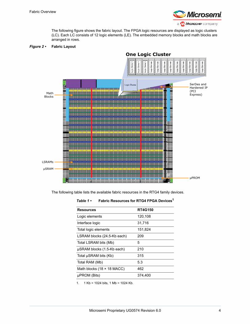
3.1.2 STMR-D Flip-FlopEach logic element has a Single-event Transient (SET)-mitigated asynchronous Self-corrected Triple Module Redundancy (STMR)-D flip-flop, which can be used as a sequential logic element. The STMR-D flip-flop can be configured as a register. The following figure shows the functional block diagram of STMR-D flip-flop. Each STMR-D flip-flop has Asynchronous majority voter logic that ensures Single-event Upset (SEU) immunity within the timeline of an SET pulse width. Its TMR mitigates the SEU errors.
The STMR-D flip-flop has the following ports:
• Asynchronous load (ALn)• Synchronous load (SLn)• Data input (D)• Enable (EN)• Clock input (CLK)• Data Output (Q)• delay_en• delay_sel[4:0]
Figure 4 • Functional Block Diagram of STMR-D Flip-Flop
ALn can be used as single global asynchronous set or reset signal of each fabric STMR-D flip-flops. It sets or resets the register depending on configuration. SLn can be used as synchronous set or reset signal of each fabric STMR-D flip-flop. It sets or resets the register depending on configuration. The data input (D) of the STMR-D flip-flop can be provided from the direct input or from the outputs of the 4-input LUT inside the logic element. When the design uses falling edge clocking, the Libero SoC Compile step optimizes the design netlist using a technique called "bubble pushing". As a result a discrete inverter instance can be removed from the netlist and the inversion property is pushed onto the CLK input pin of the SLE macro. D has a programmable delay circuit to derive a delayed data for SET mitigation. This delay circuit can be enabled or disabled using the delay_en signal. The delay_sel[4:0] signal decides the delay value for maximum SET glitch width, which can be filtered out. The radiation majority voter logic outputs the final output (Q) from the three flip-flops.
STMR-D flip-flops support Mitigated SET and Non-mitigated SET modes. These modes can be set by using the Libero SoC tool. For more information about how to set mitigation modes, see the Libero SoC Classic Constraint Flow User Guide and Libero SoC for Enhanced Constraint Flow(ECF) User Guide. Non-mitigated timing mode is significantly faster than the mitigated timing mode. Setting the fabric flip-flops in critical timing paths to Non-mitigated mode improves the application speed significantly and reduces the radiation tolerance nominally.
CLK
D
ALn
DFF0
Control
Radi
atio
n H
arde
ned
Maj
ority
Vot
er
Q
SLn
Delaydelay_sel[4:0]delay_en
DFF1
Control
Q
DFF2
Control
Q
(STMR Output) Q
CLK
CLK
CLK
EN
Microsemi Proprietary UG0574 Revision 6.0 6

Logic Elements and Routing
3.1.3 Interface LogicThe RTG4 embedded hard IP blocks (LSRAM, µSRAM, and math blocks) are connected to the fabric through interface logic (ILs). This interface logic element is structurally similar to a logic element with 4-input LUT, STMR-D flip-flop, and without a dedicated carry chain. Interface logic elements are also TMR-D and have same SET mitigation as Logic Elements. Each embedded hard IP block is associated with 36 interface logic elements. The following table lists the total number of ILs associated with each embedded hard IP block.
Figure 5 • Functional Block Diagram of Interface Logic
Figure 6 • LSRAM/µSRAM/Math Block Interfacing with ILs in a Row
If an embedded hard block is used by the target design, the interface logic element is used to connect the I/Os of the embedded hard IP block to the fabric routing. If an embedded hard IP block is not used by the design, the interface logic can be used as normal logic elements to implement combinational and sequential circuits. The preceding figure shows the interface logic connected to the embedded hard block.
3.1.4 I/O ElementThe I/O element includes the I/O Digital (IOD) circuitry and the associated routing interface. Each user I/O pad is connected to its own dedicated I/O element. The I/O element interfaces the user I/Os with the fabric routing and enables the routing of external signals coming in through the I/Os to reach all the logic elements. The I/O element also enables the internal signals to reach the I/Os.
Table 3 • ILs for Embedded Hard IP Blocks
ResourcesRT4G150
Number of Blocks Number of LEsLSRAM 209 7,524
µSRAM 210 7,560
Math block 462 16,632
Total interface logic 881 31,716
STMRFlip-Flop4-LUT
Interface Logic
D1
D2
ALn
dataD
EN
CLK SLn
Q
CBA EN CLK SLn ALn
A B C D
Y
Row
...
36 Logic Elements 36 Logic Elements
LSRAM/μSRAM/Math Block LSRAM/μSRAM/Math Block
LE
LE
LE
LE
LE
LE
LE
LE
LE
LE
LE
LE
LE
LE
LE
LE
LE
LE
LE
LE
LE
LE
LE
LE
LE
LE
LE
LE
LE
LE
LE
LE
LE
LE
LE
LE
LE
LE
LE
LE
LE
LE
LE
LE
LE
LE
LE
LE
LE
LE
LE
LE
LE
LE
LE
LE
LE
LE
LE
LE
LE
LE
LE
LE
LE
LE
LE
LE
LE
LE
LE
LE
Microsemi Proprietary UG0574 Revision 6.0 7

Logic Elements and Routing
The following figure shows the functional diagram of the complete I/O element with the IOD and I/O Analog (IOA). The IOD circuitry consists of the following:
• Input registers: Used to register the inputs received from the I/Os. These registers allow capturing the input signals and synchronizing them to the design clock.
• Output registers: Used in the I/O element for registering the output signals at I/Os for better design performance. These registers provide the registered version of the output signals to the I/Os.
• Output Enable registers: Act as a control signal for the output, if the I/O is configured as a tristate or bi-directional I/O.
• Routing multiplexers (MUXes): These routing MUXes are used to connect logic elements.All these registers in the I/O modules are similar to the STMR-D-flip-flop available in the logic element. For a signal bus, these registers ensure that all the signal bus bits are synchronized to the clock signal when sent out through I/Os. For more information on IOA, see UG0741: RTG4 FPGA I/Os User Guide.
Figure 7 • Functional Block Diagram of I/O Element
3.2 Logic ClusterThe logic elements in the RTG4 FPGA are organized in clusters. The logic cluster is a group of 12 LEs or 12 ILs. Each logic cluster is connected by a routing interface comprising MUXes and buffers. This routing interface connects to its associated LEs and the adjacent routing interfaces. Each routed signal is driven by a unique logic element output or by a routing MUX. All the logic elements are interconnected with feedback from outputs to inputs.
outreg
outreg
Output data
Output enable
OCLK
outreg
outreg
Output data
Output enable
inregRegistered input data
ICLK
n-registered input data
n-registered input data
inregRegistered input data
DO_P
OE_P
DO_N
OE_N
DI_P
DI_N
I/O Module (IOD)
ODT
ODT
PAD_P
PAD_N
IOA
01
01
DIFF_IN
DIFF_OUT
DifferentialODT
Weak pull-up/pull-down
resistor control
VREF
TX
RX
TX
RX
0 1
Microsemi Proprietary UG0574 Revision 6.0 8

Logic Elements and Routing
The following figure shows the logic cluster with routing interface.
Figure 8 • Logic Cluster
3.3 Routing ArchitectureThe RTG4 FPGA fabric routing architecture is a hierarchical grouping of fabric resources arranged in clusters. Each logic cluster has one routing interface that connects the LEs within a cluster and also to the routing interfaces of adjacent clusters.
The RTG4 device routing interface has two types of routings—intra cluster routing and inter cluster routing. The intra-cluster routing connects the LEs inside a cluster and inter-cluster routing connects multiple clusters. The intra-cluster routing has lower propagation delay compared to inter-cluster routing. When connecting the adjacent clusters, inter-cluster routing also has additional short routing connections for faster routing.
RTG4 FPGAs have vertical and horizontal routing stripes for global network. This global network is designed to route clocks and reset signals across the fabric with low skew, and is designed to support multiple clock domains. This global network can also be used for other high fan-out signals, such as enables and resets. See UG0586: RTG4 FPGA Clocking Resources User Guide for more information about global network.
Each 4-input LUT, D-type flip-flop, carry chain, LSRAM, µSRAM, and math block has individual X-Y coordinates. If the user design requires manual placement of these blocks, it is possible to set region constraints using these coordinates. The coordinates are measured from the lower left (0, 0) to the top right corner (X, Y), where X, Y values vary as per the device.
For more information about using coordinates for region/placement constraints, see the Chip Planner User’s Guide or Libero SoC Online Help.
The array coordinates are measured from the bottom left corner to the top right corner of the FPGA fabric. The following table provides the array coordinates of logical blocks and embedded hard blocks of the RTG4 devices. For more information about how to use array coordinates for region or placement constraints, see Libero SoC Classic Constraint Flow User Guide and Libero SoC for Enhanced Constraint Flow(ECF) User Guide or online help (available in the software).
Table 4 • Fabric Array Coordinate Systems
DeviceLogic Elements µSRAM LSRAM Math BlocksMinimum (X, Y) Maximum (X, Y) (X, Y) (X, Y) (X, Y)
RT4G150 0, 0 1535, 311 (0, 56), (0,125),(0, 182), (0, 212),(0, 266)
(0, 32), (0, 95),(0, 158),(0, 236), (0, 296)
(0, 17), (0, 41), (0, 71),(0, 80), (0, 110),(0, 140), (0, 167),(0, 197), (0, 221),(0, 251), (0, 281)
Routing InterfaceAdjacent Routing Interface
Adjacent Routing
Interface
LUT
FF
LUT
FF
LUT
FF
LUT
FF
LUT
FF
LUT
FF
LUT
FF
LUT
FF
LUT
FF
LUT
FF
LUT
FF
LUT
FF
LE LE LE LE LE LE LE LE LE LE LE LECarry In Carry Out
Logic Cluster
Microsemi Proprietary UG0574 Revision 6.0 9

Logic Elements and Routing
3.4 Libero Compile Report - Fabric ResourcesThe compile report contains fabric resource utilization and the total number of resources available. See the following figure for a sample compile report for RT4G150. This report provides the number of 4LUTs, DFFs, µSRAMs, LSRAMs, math blocks, I/O, DLLs, PLLs, transceivers, and globals used in a design. It also contains the detail logic resource usage that contains the additional 4LUTs and DFFs required for RAMs and MACC interface logic.
Figure 9 • Sample Compile Report for RT4G150
Microsemi Proprietary UG0574 Revision 6.0 10

Embedded Memory Blocks
4 Embedded Memory Blocks
The RTG4 FPGA fabric has the following memory blocks:
• LSRAM: The embedded 24-Kb SRAM blocks are arranged in multiple rows within the fabric and can be accessed through the fabric routing architecture. The LSRAMs can be operated in dual-port or two-port modes. The following table lists the number of available LSRAM blocks depending on the specific RTG4 device. LSRAM blocks are used for storing large data with Error-correcting Code (ECC) and Single-event Transient (SET) mitigation options.
• µSRAM: The embedded 1.5-Kb SRAM blocks are arranged in multiple rows within the fabric and can be accessed through the fabric routing architecture. The following table lists the number of available µSRAM blocks depending on the specific RTG4 device. Embedded µSRAM blocks are used for storing small data with ECC and SET mitigation options.
• µPROM: The embedded non-volatile PROM is arranged in a single row at the bottom of the fabric and is read only through the fabric interface. The µPROM can be loaded only during device programming.
The following table lists the LSRAM, µSRAM, and µPROM features.
Note: In specific configurations, x9 and x12 dual-port LSRAMs undergo compile transformations by Libero SoC. See, Customer Advisory Notice (CAN) 18002.3. Compile transformations occur when opening a design created by an older version of Libero or when compiling a design that contains manually instantiated LSRAM primitive macros.
Table 5 • RTG4 LSRAM, µSRAM, and µPROM Features
Feature LSRAM µSRAM µPROMMemory size 24,576 bits/block 1,536 bits/block 374,400 bits (total
memory size)
Data bus width 512 × 36, 1K × 18, 2K × 12, 2K × 91
1. Only the ×12 port width accesses the entire address space of the 24,576 bits. The ×9, ×18, and ×36address space is limited to 18,432 bits.
64 × 18, 128 × 12, 128 × 92
2. Only the ×12 port width accesses the entire address space of the 1536 bits. The ×9 and ×18 addressspace is limited to 1152 bits.
16K × 36
Number of ports 2 read/write ports in dual port mode
2 read ports, 1 write port 1 read port
Memory modes True dual-port3 and two-port
3. True dual-port is not available for 2K x 12 and 2K x 9.
Three-port Single-port
Read operation Synchronous Synchronous/Asynchronous Synchronous
Write operation Simple write Simple write Only during device programming
ECC Available for ×18 data widths in dual-port mode and for ×18, ×36 data widths in two-port mode.
Available for ×18 data widths
Microsemi Proprietary UG0574 Revision 6.0 11

Embedded Memory Blocks
The following table lists the embedded memory resources available in RTG4 devices.
4.1 LSRAMEach LSRAM has two independent ports—port A and port B, as shown in the following figure. Both these ports support write and read operations and can be configured in dual-port mode or two-port mode depending on the data width and access pattern requirement. LSRAMs follow the little-endian system.
Figure 10 • Functional Block Diagram of LSRAM
Table 6 • RTG4 Embedded Memory Resources
Resources RT4G15024.5-Kb LSRAM blocks 209
LSRAM (Mb)1
1. 1 Kb = 1024 bits, 1 Mb = 1024 Kb.
5
µSRAM blocks (1.5-Kb each) 210
µSRAM (Kb)1 315
Total RAM (Mb)1 5.3
µPROM (Bits) 374,400
A_DOUT[17:0]
PipelineRegister
A_DIN[17:0]
B_DIN[17:0]
A_ADDR[10:0]A_WEN[1:0]A_BLK[2:0]
A_CLK
Port A Row decodeWrite Control
Port B Row decodeWrite Control
Column Decode
Column Decode
ECC_EN
B_DOUT[17:0]
Memory Array1K x 24
ECCLogic
ECCLogic
A_DOUT_EN
B_REN
A_SB_CORRECT
A_DB_DETECT
B_SB_CORRECT
B_DB_DETECTB_DOUT_EN
A_REN
ECC Logic
ECC_EN
ECC Logic
ECC_EN
B_ADDR[10:0]B_WEN[1:0]B_BLK[2:0]
B_CLK
PipelineRegister
ECC_EN
A_CLK A_DOUT_SRST_N
ARST_N
B_CLK B_DOUT_SRST_N
ARST_N
A_DOUT_BYPASS
B_DOUT_BYPASS
Microsemi Proprietary UG0574 Revision 6.0 12
Embedded Memory Blocks
The following table lists the port list for LSRAM.
Table 7 • Port List for LSRAM
Port Name Direction Type1 Polarity DescriptionPort AA_ADDR[10:0] Input Dynamic Port A address
A_BLK[2:0] Input Dynamic Active high Port A block selects
A_CLK Input Dynamic Rising edge Port A clock
A_DIN[17:0] Input Dynamic Port A write-data
A_DOUT[17:0] Output Dynamic Port A read-data
A_WEN[1:0]2 Input Dynamic Active high Port A write-enables (per byte)
A_REN Input Dynamic Active high Port A read-enable
A_WIDTH[1:0] Input Static Port A width/depth mode select
A_WMODE[1:0] Input Static Active high Port A write mode select. Must be 2'b00.
A_DOUT_BYPASS Input Static Active low Port A output pipeline bypass mode
A_DOUT_EN Input Dynamic Active high Port A read pipeline register enable
A_DOUT_SRST_N Input Dynamic Active low Port A read pipeline synchronous-reset
A_SB_CORRECT Output Dynamic Active high Port A 1-bit error correction flag
A_DB_DETECT Output Dynamic Active high Port A 2-bit error detection flag
Port BB_ADDR[10:0] Input Dynamic Port B address
B_BLK[2:0] Input Dynamic Active high Port B block selects
B_CLK Input Dynamic Rising edge Port B clock
B_DIN[17:0] Input Dynamic Port B write-data
B_DOUT[17:0] Output Dynamic Port B read-data
B_WEN[1:0]2 Input Dynamic Active high Port B write-enables (per byte)
B_REN Input Dynamic Active high Port B read-enable
B_WIDTH[1:0] Input Static Port B width/depth mode select
B_WMODE[1:0] Input Static Active high Port B write mode select. Must be 2’b00.
B_DOUT_BYPASS Input Static Active low Port B pipeline register select
B_DOUT_EN Input Dynamic Active high Port B pipeline register enable
B_DOUT_SRST_N Input Dynamic Active low Port B pipeline synchronous-reset
B_SB_CORRECT Output Dynamic Active high Port B 1-bit error correction flag
B_DB_DETECT Output Dynamic Active high Port B 2-bit error detection flag
Common SignalsARST_N Input Global Active low Pipeline registers asynchronous-reset
ECC_EN Input Static Active high ECC enable, turns on the ECC encoders, decoders, and registers.
ECC_DOUT_BYPASS Input Static Active low ECC pipeline bypass
DELEN Input Static Active high SET mitigation
SECURITY Input Static Active high Lock access to system controller3
Microsemi Proprietary UG0574 Revision 6.0 13

Embedded Memory Blocks
4.1.1 Dual-Port ModeThe LSRAM block can be configured as a true dual-port SRAM with independent write and read ports. Write and read operations can be performed from both the ports (A and B) independently at any location as long as there is no write collision. The LSRAM block does not have built-in write collision detection circuit. Simultaneous read and write operations from both ports to the same address location results in correct data written into the memory, but does not guarantee correct read data. Each port has a unique address, data in, data out, clock, block select, write enable, pipeline registers.
4.1.1.1 Dual-Port Data Width ConfigurationIn dual-port mode, both ports A and B have maximum data width of ×18. Each port can be configured in multiple data widths. The configuration of one port has a corresponding configuration for the other port, as shown in the following table. A_WIDTH indicates the read width and B_WIDTH indicates the write width.
4.1.1.2 Dual-Port Block Select OperationIn dual-port mode, to perform two independent write and read operations (on port A or port B or both) the block select signal is required. The following table lists the block select operation for port A and port B. When the pipeline registers are enabled, the effect of the block select at the outputs is delayed by one clock cycle, see Figure 11.
BUSY Output Dynamic Active high Busy signal from the system controller. This is high while system controller accessing LSRAM.3
1. Static inputs are defined during the design time and must be tied to logic 0 or 1.2. If the LSRAM block is configured for data width of x9 or ECC, both the bits of A_WEN and B_WEN must be tied to logic 1 and
must not be dynamically changed.3. For more information about BUSY signal from system controller, see UG0576: RTG4 FPGA System Controller User Guide.
Table 8 • Data Width Configurations For Dual-port Mode
A_WIDTH B_WIDTH×9 ×18
×18 ×18
Table 9 • Block Select Operation
A_BLK[2:0] B_BLK[2:0] OperationAny one bit = 0 Any one bit = 0 No operation on port A or B. The data output
A_DOUT[17:0] and B_DOUT[17:0] will be forced zero.
Any one bit = 0 111 Read or write operation on port B. A_DOUT[17:0] will be forced zero.
111 Any one bit = 0 Read or write operation on port A. B_DOUT[17:0] will be forced zero.
111 111 Read or write operation on both ports A and B.
Table 7 • Port List for LSRAM (continued)
Port Name Direction Type1 Polarity Description
Microsemi Proprietary UG0574 Revision 6.0 14

Embedded Memory Blocks
Figure 11 • Block Select Inputs for Dual-Port Mode
4.1.1.3 Dual-Port Byte Write EnablesThe byte write enables (A_WEN[1:0] and B_WEN[1:0]) enable writing individual bytes of data (9 MSB or 9 LSB) for the ×18 width. The byte write enables for port A (A_WEN[1:0]) enable A_DIN[17:9] and A_DIN[8:0] respectively. The byte write enables for port B (B_WEN[1:0]) enable B_DIN[17:9] and B_DIN[8:0] respectively. Writing one byte at a time to the LSRAM is not compatible with the built-in ECC logic, as per Table 14, page 21. The complete data word must be written by setting both WEN bits high when using the built-in LSRAM ECC.
If all byte write enables are low, then port A or port B is considered to be in read mode and any read operations are controlled by the read enables (A_REN and B_REN).
The following table lists the byte write enable settings for port A and port B.
4.1.1.4 Dual-Port Read EnableThe read enable signals, A_REN and B_REN, perform the read operation on port A and port B, unless any one bit of that port's block select is low which forces the data outputs to low. When read enable is low, the data outputs retain their previous state and no dynamic read power is consumed on that port. When read enable is high, LSRAM performs read operation and consumes read power.
4.1.2 Two-Port Mode The LSRAM block can be configured as a two-port SRAM with port A dedicated to read operations and port B dedicated to write operations. For data widths greater than ×18, the read port borrows the port B data output signals, similarly write port borrows the port A data input signals.
Figure 12 illustrates the two-port LSRAM data-flow in the x36 data width configuration.
Table 10 • Dual-Port Byte Write Enables Settings
Depth x Width A_WEN / B_WEN Result2K×9, 1K×18 00 Perform a read operation
2K×9 11 Perform a write operation
1K×18 01 Write [8:0]
10 Write [17:9]
11 Write [17:0]
A_CLKB_CLK
A_BLKB_BLK
Non-Pipeline DOUT Mode
B_DOUT[17:0] A_DOUT[17:0]
B_DOUT[17:0] A_DOUT[17:0]
Pipeline DOUT Mode
Clock Cycle #1 Clock Cycle #2 Clock Cycle #3
Microsemi Proprietary UG0574 Revision 6.0 15

Embedded Memory Blocks
Figure 12 • Two Port Mode x36 Data Flow
Port B Write Column Decoding
Memory Array(128 rows x 192
columns)
Port
A (re
ad) R
ow
Dec
oder
Port
A(re
ad) R
ow P
re-
Dec
oder
+ A
ddre
ss
Latc
h
Port
B(w
rite)
Row
D
ecod
er
Port
B(w
rite)
Row
Pre
-D
ecod
er +
Add
ress
La
tch
Port A Data Input Latch
B_WIDTH[1:0]
B_BLK[2:0]
B_CLK
A_WEN[1:0]
A_DIN[17:0]
A_ADDR[10:2]B_ADDR[10:2]
ECCLogic
Port
B (w
rite)
Tim
ing
and
Con
trol L
ogic
Port A Write Driver
Port A Read Column Decoding
A_WIDTH[1:0]
A_BLK[2:0]
A_CLK
A_REN
Port
A(re
ad) R
ow T
imin
g an
d C
ontro
l Log
ic
Port B Data Input Latch
Port B Write Driver
ECCLogic
Port A Sense Amp & Latch
Port A Pipe Line Register
ECC Flag Register
Port B Sense Amp & Latch
Port B Pipe Line Register
ECC Flag Register
B_DIN[17:0]
DATA_IN <35:18><17:0>
A_DOUT[17:0] B_DOUT[17:0]B_SB_CORRECT
A_DB_DETECT
A_SB_CORRECT
B_DB_DETECT
DATA_OUT <35:18><17:0>
A_DOUT_BYPASS B_DOUT_BYPASS
B_WEN[1:0]
ECCLogic
ECCLogic
Microsemi Proprietary UG0574 Revision 6.0 16

Embedded Memory Blocks
4.1.2.1 Two-Port Data Width ConfigurationIn two-port mode, the maximum data width is ×36. Each port can be configured in multiple data widths. The configuration of read port has a corresponding configuration for the write port, as shown in the following table.
Note: Libero SoC performs compile transformations on two-port LSRAMs configured for x9 and x12 write widths where the writes occur on port B. For more information, see Customer Advisory Notice (CAN18002.3). These configurations will have the read and write ports swapped so that writes occur on port A instead of port B.
4.1.2.2 Two-Port Block Select OperationIn the two-port mode Port A is the read port and Port B is the write port. Table 12, page 17 lists the Block select values required to enable the read and write operation on Port A and Port B respectively.
4.1.2.3 Two-Port Byte Write EnablesThe byte write enables (A_WEN and B_WEN) enable writing individual bytes of data (9 MSB or 9 LSB) for ×9 width, ×18, and ×36 data widths. For ×36 write-width, the byte write enables for the corresponding data is used to enable each of the four bytes, that is, byte write enables for port A enable A_DIN[17:9] and A_DIN[8:0] and byte write enables for port B enable B_DIN[17:9] and B_DIN[8:0]. Writing one byte at a time to the LSRAM is not compatible with the built-in ECC logic, as per Table 14, page 21. The complete data word must be written by setting all WEN bits high when using the built-in LSRAM ECC.
The following table lists the byte write enable settings for port A and port B.
4.1.2.4 Two-Port Read EnableThe read enable signals, A_REN and B_REN, perform the read operation on port A and port B, unless any one bit of A_BLK is low which forces the data outputs to low. When read enable is low, the data outputs retain their previous state and no dynamic read power is consumed on that port. When read
Table 11 • Data Width Configurations for Two-Port Mode
Read Port Write Port×9 ×9, ×18, ×36
×12 ×12
×18 ×9, ×18, ×36
×36 ×18, ×36
Table 12 • Block Select Operation in Two-Port Mode
A_BLK[2:0] Setting Read Operation B_BLK[2:0] Setting Write OperationA_BLK[2:0]=111 Read operation from Port A. B_BLK[2:0]=111 Write operation at the Port B.
Any bit of A_BLK[2:0] is 0
No read operation from Port A. The data outputs A_DOUT[17:0] and B_DOUT[17:0] are forced to zero.
Any bit of B_BLK[2:0] is 0 No write operation at the Port B.
Table 13 • Two-Port Byte Write Enables For x36 Write Width
Depth x Width A_WEN/B_WEN Result
512×36
B_WEN[0] = 1 Write B_DIN[8:0]
B_WEN[1] = 1 Write B_DIN[17:9]
A_WEN[0] = 1 Write A_DIN[8:0]
A_WEN[1] = 1 Write A_DIN[17:9]
Microsemi Proprietary UG0574 Revision 6.0 17

Embedded Memory Blocks
enable is high, LSRAM performs read operation and consumes read power. When read width is x36, LSRAM port B read enable (B_REN) is tied to port A read enable (A_REN).
4.1.3 LSRAM Read OperationLSRAM supports both pipelined and non-pipelined read operations. In pipelined read operation, the output data is registered at the pipeline registers; hence, the data is available on the corresponding data output on the next clock cycle. Figure 13 shows the pipelined and non-pipelined read timing.
In non-pipelined read operation, the pipeline registers are bypassed with data available on the corresponding output in the same clock cycle. During this operation, LSRAM can generate glitches on the data output buses. Therefore, it is recommended to use LSRAM with pipeline registers to avoid glitches.
Note: Enable pipeline mode to achieve high performance. This will pipeline the output data bus before the data bus is delivered to the FPGA fabric.
Note: When using non-pipelined ECC mode, the SET filter must be enabled per the Product Change Notification (PCN 18009.1). If this filter is not enabled by the user, Libero SoC (v11.9 and above) automatically turns on SET mitigation for non-pipelined ECC LSRAMs.
Figure 13 shows both pipelined and non-pipelined read operations.
Figure 13 • LSRAM Read Operation
4.1.4 LSRAM Write OperationLSRAM supports Simple write operations:
A_ADDR[10:0]B_ADDR[10:0]
A_BLK[2:0]B_BLK[2:0]
A_DOUT[17:0] B_DOUT[17:0]
A_DOUT[17:0] B_DOUT[17:0]
Pipelined access or non-pipeline access with pipelined ECC1
Non-pipeline mode without ECC
A0 A1 A2
D(A0) D(A1) D(A2)
D(A1)D(A0)
A_DOUT[17:0] B_DOUT[17:0]
Pipelined access with non-pipelined ECC
A_DOUT[17:0] B_DOUT[17:0]
Pipelined access with ECC pipeline1
SB_CORRECTDB_DETECT
Corresponding ECC Flag Outputs
SB_CORRECTDB_DETECT
Corresponding ECC Flag Outputs
Data in Address A0
SB_CORRECTDB_DETECT
Corresponding ECC Flag Output
1. For cases where pipelined ECC mode is used, the first write cycle is used by the ECC encoder and the second clock cycle is used when the LSRAM memory array is actually written. Therefore, it is not legal to perform a write immediately followed by a read to the same address on the next clock cycle, because the LSRAM is being written with the newly encoded data. When pipelined ECC mode is used, after issuing a write to a given LSRAM address, a subsequent read to that address must wait until two clock cycles later to ensure the correct data is being read. Once the read command is issued, pipelined ECC mode requires one clock cycle to decode the data from LSRAM before it is presented on the data output port.
D(A3)
A3
A_CLKB_CLK
Clock Cycle #1 Clock Cycle #2 Clock Cycle #3 Clock Cycle #4
A_WEN[1:0]B_WEN[1:0]
A_REN]B_REN]
D(A2) D(A3)
D(A0)
A4
D(A1)D(A0) D(A2) D(A3)
Non-Pipeline mode with Non-Pipelined ECCA_DOUT[17:0] B_DOUT[17:0]
D(A0) D(A1) D(A2)
D(A4)
D(A3)
Microsemi Proprietary UG0574 Revision 6.0 18

Embedded Memory Blocks
In a simple-write operation, data input A_DIN and B_DIN are written to the corresponding address locations A_ADDR and B_ADDR. The data written to the memory is available at the output only after performing a read operation.
Note: Simultaneous write operations from both ports to the same address location are not prevented. Since simultaneous write operations can result in data uncertainty, it is recommended to use external logic in the fabric to avoid collisions.
The following figure shows the timing for write operations followed by the corresponding read to the same address, at the earliest possible time.
Figure 14 • LSRAM Write Operation— Followed by Earliest Read
A_CLKB_CLK
A_ADDR[10:0]B_ADDR[10:0]
A_BLK[2:0]B_BLK[2:0]
A_DOUT[17:0] B_DOUT[17:0]
A_DOUT[17:0] B_DOUT[17:0]
Pipelined Read with non-pipelined ECC
Non-pipeline mode without ECC
A0
Clock Cycle #1 Clock Cycle #2
D(A0)
A_DOUT[17:0] B_DOUT[17:0]
SB_CORRECTDB_DETECT
Corresponding ECC Flag Outputs
Non-Pipelined Read with Pipelined ECC
D(A0)=Data in Address A0
SB_CORRECTDB_DETECT
Corresponding ECC Flag Outputs
A_DIN[17:0]B_DIN[17:0]
1.For cases where pipelined ECC mode is used, the first write cycle is used by the ECC encoder and the second clock cycle is used when the LSRAM memory array is actually written. Therefore, it is not legal to perform a write immediately followed by a read to the same address on the next clock cycle, because LSRAM is being written with the newly encoded data. When using pipelined ECC mode, after issuing a write to a given LSRAM address, a subsequent read to that address must wait until two clock cycles later to ensure the correct data is being read. Once the read command is issued, pipelined ECC mode requires one clock cycle to decode the data from LSRAM before it is presented on the data output port.
A_WEN[1:0]B_WEN[1:0]
D0
A_RENB_REN
D(A0) D(A0)
A_DOUT[17:0] B_DOUT[17:0]
Pipelined read without ECC
D(A0)
D(A0)
A_RENB_REN
Read Enable during Pipelined ECC
A_DOUT[17:0] B_DOUT[17:0]
Pipelined Read with ECC Pipelined
SB_CORRECTDB_DETECT
Corresponding ECC Flag Outputs
D(A0) D(A0)
A0
Clock Cycle #3 Clock Cycle #4
A0
Microsemi Proprietary UG0574 Revision 6.0 19

Embedded Memory Blocks
4.1.5 Pipelined Read Synchronous Reset OperationEach port's pipeline registers have a synchronous reset. A_DOUT_SRST_N and B_DOUT_SRST_N drive the synchronous reset of the data output pipeline registers: A_DOUT and B_DOUT. If the synchronous reset is low, the pipeline data output registers are reset to zero on the next valid clock edge, as shown in the following figure.
Figure 15 • LSRAM Synchronous Reset Operation
4.1.6 Pipelined Read Asynchronous Reset OperationEach LSRAM has an asynchronous reset (ARST_N), which connects the read-data pipeline registers to the global asynchronous-reset signal. If the asynchronous reset is driven low, the pipeline data registers are immediately reset to zero as shown in the following figure.
A_CLKB_CLK
A_DOUT_SRST_N B_DOUT_SRST_N
A_DOUT[17:0]B_DOUT[17:0]
A_DOUT[17:0]B_DOUT[17:0]
Non-pipeline mode
Pipeline mode
Clock Cycle #1 Clock Cycle #2
Microsemi Proprietary UG0574 Revision 6.0 20

Embedded Memory Blocks
Figure 16 • LSRAM Asynchronous Reset Operation
4.1.7 LSRAM ECCThe LSRAM block has ECC logic circuitry (1-bit error correction, 2 bits error detection) for the ×18 and ×36 modes; but not for the ×9 and ×12 modes. The error correction code (ECC) encoder provides 24 bits of data for ×18 mode or 48 bits of data for ×36 mode. The ECC decoder reads the same amount of bits (24 or 48) from the array and provides the expected number of corrected bits (18 or 36) on the outputs. The ECC encoder contains an optional pipeline register which is enabled during pipelined ECC mode. The ECC encoder pipeline register delays the actual data write to the LSRAM by 1 clock cycle.
Table 14 • ECC Available Mode
Port Widths A/B
Write Enables(byte write) Output Pipeline Pipeline Bypass
×9/×9 No ECC No ECC No ECC
×9/×18 No ECC No ECC No ECC
×9/×36 No ECC No ECC No ECC
×12/×12 No ECC No ECC No ECC
×18/×9 No ECC No ECC No ECC
×18/×18 No ECC ECC available ECC available
×18/×36 No ECC ECC available ECC available
×36/×9 No ECC No ECC No ECC
A_CLKB_CLK
ARST_N
A_DOUT[17:0]B_DOUT[17:0]
A_DOUT[17:0]B_DOUT[17:0]
SB_CORRECTB_DETECT
SB_CORRECTDB_DETECT
A_DOUT[17:0]B_DOUT[17:0]
SB_CORRECTDB_DETECT
A_DOUT[17:0]B_DOUT[17:0]
A_DOUT[17:0]B_DOUT[17:0]
Pipeline mode with pipelined ECC
Pipeline mode with pipelined ECC
Pipeline mode with non-pipelined ECC
Non-pipeline mode with pipelined ECC
Non-pipeline mode with pipelined ECC
Pipeline mode without ECC
Non-pipeline mode with non-pipelined ECC
Non-pipeline mode with non-pipelined ECC
Non-pipeline mode without ECC
Clock Cycle #1 Clock Cycle #2
A_DOUT[17:0]B_DOUT[17:0]
Microsemi Proprietary UG0574 Revision 6.0 21
Embedded Memory Blocks
For cases where pipelined ECC mode is used, the ECC encoder, used during writes, and the ECC decoder, used during reads, will each add a clock cycle to the memory operations. During a write to a pipelined ECC LSRAM, the first write cycle is used by the ECC encoder and the second clock cycle is where the LSRAM memory array is actually written. Therefore, it is not legal to perform a write immediately followed by a read to the same address on the next clock cycle, because that is the same cycle where the LSRAM is being written with the newly encoded data. When using pipelined ECC mode, after issuing a write to a given LSRAM address, a subsequent read to that address must wait at least two clock cycles to ensure the correct data is being read. Once the read command is issued, pipelined ECC mode requires one clock cycle to decode the data from LSRAM before it is presented on the data output port. The following are the possible scenarios, since the output data can also be pipelined.
• Pipeline mode with non-pipelined ECC• Pipeline mode with pipelined ECC• Non-pipeline mode with non-pipelined ECC• Non-pipeline mode with pipelined ECCThe timing diagrams for the above possible scenarios are shown in Figure 14.
The ECC logic generates two flags:
• SB_CORRECT: Asserted when a single-bit error is detected. If SB_CORRECT is set without the dual-bit error flag being asserted, the corrupted bit is corrected in read data output. Even though the corrupted bit is corrected in the read data output, the data in the RAM location is not corrected. The user logic must correct the contents of the RAM.
• DB_DETECT: Asserted when a dual-bit error is detected, but not corrected. Multi-bit errors (more than two bits) produce unknown results on the flags and data outputs. If DB_DETECT is set, correction is not performed on read data output. Correction must be performed by user logic.
In pipeline mode, these flags are valid only in read data output clock cycle. In non-pipeline mode, the ECC flags are valid only in the same clock cycle as the corresponding read data output, because they are reset in the next clock cycle.
The following table lists the ECC errors and corresponding flag status.
During an x36 read with LSRAM ECC enabled, all the A and B port ECC flags are used to represent the ECC status for the complete x36 read data out word.
Note: The ECC decoder generates two flags (DB_DETECT and SB_CORRECT). If a single-bit error occurs in a 24-bit word (18 data bits and 6 ECC bits), the error correction flag (SB_CORRECT) is set high and the 18-bit data is corrected. If two or multiple-bit errors occur in the 24-bit word, DB_DETECT and SB_CORRECT flags are set high and the 18-bit data from the LSRAM is not corrected or modified. If multiple-bit errors occur in the 6 ECC bits, both ECC flags are asserted and no correction is performed on the 18-bit data.
4.1.8 Using LSRAM in a DesignAn LSRAM block can be implemented in a design by the following methods:
×36/×18 No ECC ECC available ECC available
×36/×36 No ECC ECC available ECC available
Table 15 • LSRAM Error Flag Status
ECC Errors SB_CORRECT DB_DETECTNo error 0 0
Single-bit error 1 0
Double-bit error 1 1
Table 14 • ECC Available Mode (continued)
Port Widths A/B
Write Enables(byte write) Output Pipeline Pipeline Bypass
Microsemi Proprietary UG0574 Revision 6.0 22

Embedded Memory Blocks
• RTL Inference during Synthesis• Inserting an LSRAM Configurator Component
4.1.8.1 RTL Inference during SynthesisSynplify Pro can infer an LSRAM and automatically set the configuration for various modes, if the RTL design contains an array of at least 12 bits. Synplify also supports inferring memories according to the user attribute syn_ramstyle. Synthesis ensures that the signals of the LSRAM are properly connected to the rest of the design and sets the correct values for the static signals required to configure the appropriate operational mode. The tool ties unused dynamic input signals to low.
Note:
Synplify Pro can cascade multiple LSRAM blocks if the required memory size exceeds the limit of a single LSRAM block. It can also absorb any registers at the LSRAM interface if they are driven by the same clock. If the registers have different clocks, then the clock that drives the output register has priority, and all registers driven by that clock are absorbed into the LSRAM block. If the outputs are unregistered and the inputs are registered with different clocks, the input registers with the larger input have priority and are absorbed into the LSRAM block. For more information about LSRAM inference by Synplify Pro, see Inferring Microsemi RTG4 RAM Blocks Application Note.
4.1.8.2 Inserting an LSRAM Configurator ComponentThe Libero SoC software catalog provides separate configuration tools for dual-port and two-port modes. Using these configurators, the user can configure LSRAM in the required operating modes. These configuration tools generate the HDL wrapper files for LSRAM with the appropriate values assigned to the static signals. The generated HDL wrapper files can be used in the design hierarchy by connecting the ports to the rest of the design.
4.1.8.2.1 RTG4 Dual-Port LSRAM ConfiguratorThe RTG4 DPSRAM configurator is available in the Libero SoC IP catalog under Memory & Controllers, see Figure 17. The RTG4 DPSRAM IP configurator enables write and read access on both ports: port A and port B.
The DPSRAM configurator automatically cascades LSRAM blocks to create wider and deeper memories by selecting the most efficient aspect ratio. It also handles the grounding of unused bits. The core configurator supports the generation of memories that have different aspect ratios on each port. The configurator uses one or more memory blocks to generate a RAM component to match the configuration. The configurator also creates the external logic required for the cascading.
The configurator cascades RAM blocks in three different methods:
• Cascaded deep. For example, two blocks of 1024x18 to create a 2048x18.• Cascaded wide. For example, two blocks of 1024x18 to create a 1024x36.• Cascaded wide and deep. For example, four blocks of 1024x18 to create a 2048x36, in two blocks
width-wise by two blocks depth-wise configuration.Dual-port LSRAM is synchronous for memory write and read operations, setting up the addresses, and writing and reading the data. The memory write and read operations will be triggered at the rising edge of the clock. Optional pipeline registers are available at both read data ports to improve the clock-to-output delay.
Microsemi Proprietary UG0574 Revision 6.0 23
Embedded Memory Blocks
Figure 17 • LSRAM Ports Configured as Dual-Port SRAM - DPSRAM Macro in Libero SoC
Table 16 • Port List for the DPSRAM Configurator
Port Name Direction DescriptionPort AA_CLK Input Input clocks for port A. The same clock also acts as clock inputs for the output
pipeline registers if configured as registers. All inputs must be set up before the rising edge of the clock. The read or write operation begins with the rising edge.
A_ADDR Input Address inputs for port A.
A_BLK Input Block-select for port A.
A_DIN Input Data inputs for port A.
A_WEN Input Write enable for port A. Low = Read, High = Write.
A_REN Input Read enable for port A (exposed only if there is no depth cascading).
A_WBYTE_EN Input Port A Write Byte Enables (per byte).
A_DOUT Output Data outputs for port A.
A_DOUT_EN Input Read pipeline register enable for port A.
A_DOUT_SRST_N Input Read pipeline register synchronous reset for port A.
ARST_N Input Read pipeline register asynchronous reset for Port.
A_SB_CORRECT Output Single-bit error correction flag for port A.
A_DB_DETECT Output Double-bit error detection flag for port A.
Port BB_CLK Input Input clocks for port B. The same clock also acts as clock inputs for the output
pipeline registers if configured as registers. All inputs must be set up before the rising edge of the clock. The read or write operation begins with the rising edge.
B_ADDR Input Address inputs for port B.
B_BLK Input Block-select for port B.
B_DIN Input Data input for port B
B_WEN Input Write enable for port B. Low = Read; High = Write
B_REN Input Read enable for port B (exposed only if there is no depth cascading).
B_WBYTE_EN Input Port B Write Byte Enables (per byte).
Microsemi Proprietary UG0574 Revision 6.0 24

Embedded Memory Blocks
In this section, it is described how to configure a dual-port LSRAM instance and define how the signals are connected.
Figure 18 • Dual-Port Large SRAM Configurator
Optimization for High Speed or Low Power
The user can optimize the LSRAM macro with one of the following options:
• High Speed - To optimize the LSRAM macro for speed and area by using width cascading.• Low Power - To optimize the LSRAM macro for low power, but it uses additional logic at the input
and output by using depth cascading. Performance for a low power optimized macro may be inferior to that of a macro optimized for speed.
Port A Depth/Width and Port B Depth/Width
The user can set depth and width of a port.
• Depth - To set depth range. The depth range for each port is 1 to 32768• Width - To set width range. The width range for each port is 1 to 3762.
B_DOUT Output Data outputs for port B.
B_DOUT_EN Input Read pipeline register enable for port B.
B_DOUT_SRST_N Input Read pipeline register synchronous reset for port B.
B_SB_CORRECT Output Single-bit error correction flag for port B.
B_DB_DETECT Output Double-bit error detection flag for port B.
Common SignalsARST_N Input Pipeline registers asynchronous reset.
Table 16 • Port List for the DPSRAM Configurator (continued)
Port Name Direction Description
Microsemi Proprietary UG0574 Revision 6.0 25
Embedded Memory Blocks
Note: The two ports can be configured independently for any depth and width. Port A depth × port A width must be equal to port B depth × port B width.
Single Clock (CLK) or Independent Clocks (A_CLK and B_CLK)
The user can set the clock signals:
• Check Single Clock to drive both A and B ports with the same clock. This is the default configuration for dual-port LSRAM. Uncheck Single Clock to enable independent clock for each port: port A - A_CLK and port B - B_CLK.
• Click the waveform next to any of the clock signals to toggle its active edge.Block Select (A_BLK and B_BLK) and Read/Write Control (A_WEN and B_WEN)
De-asserting A_BLK forces A_DOUT to zero. De-asserting B_BLK forces B_DOUT to zero.
• Asserting A_BLK when A_WEN is low reads the RAM at the A_ADDR onto the input of the A_DOUT register, on the next rising edge of A_CLK.
• Asserting A_BLK when A_WEN is high writes the data A_DIN into the RAM at the A_ADDR, on the next rising edge of A_CLK.
• Asserting B_BLK when B_WEN is low, reads the RAM at the B_ADDR onto the input of the B_DOUT register, on the next rising edge of B_CLK.
• Asserting B_BLK when B_WEN is high, writes the data B_DIN into the RAM at the B_ADDR, on the next edge of B_CLK.
The default configuration for A_BLK and B_BLK is unchecked, which ties the signal to the active state and removes it from the generated macro. Click the respective checkbox to insert that signal on the generated macro. Click the signal arrow (when available) to toggle its polarity.
Pipeline for Read Data Output of Port A and B
Check the A_DOUT Pipeline or B_DOUT Pipeline checkbox to enable pipelining of read data (A_DOUT or B_DOUT). If the checkbox is not checked, the user cannot configure the A_DOUT_EN/B_DOUT_EN, A_DOUT_SRST_N/B_DOUT_SRST_N signals.
DOUT on Write
• Previous DOUT - The default data on the read data output (A_DOUT or B_DOUT) during a write cycle is the DOUT data from the previous cycle (Previous DOUT).
Note: DOUT on Write selection is ignored during read operation. Writing different data to the same address using both ports is undefined and must be avoided. Writing to and reading from the same address is undefined and must be avoided.
Register Enable (A_DOUT_EN and B_DOUT_EN)
The pipeline registers for ports A and B have active high, enable inputs. The default configuration is to tie these signals to the active state and remove them from the generated macro. Use the signal arrow (when available) to toggle its polarity.
Synchronous Reset (A_DOUT_SRST_N and B_DOUT_SRST_N)
The pipeline registers for ports A and B have active low, synchronous reset inputs. The default configuration is to tie these signals to the inactive state and remove them from the generated macro. Use the signal arrow (when available) to toggle its polarity.
Read Enable (A_REN and B_REN)
De-asserting A_REN holds the previous read data on port A and de-asserting B_REN holds the previous read data on port B. For DOUT hold behavior when using pipelined-ECC mode and REN inputs, see LSRAM Hold Time Violation, page 31. Asserting the A_REN reads the RAM at the A_ADDR onto port A's Read Data register on the next rising edge of the clock. Similarly, asserting the B_REN reads the RAM at the B_ADDR onto port B's Read Data register on the next rising edge of the clock.
The default configuration for the A_REN or B_REN checkbox is unchecked, which ties the signal to the active state and removes it from the generated macro. Check A_REN or B_REN checkbox (when available) to insert that signal on the generated macro; click the signal arrow (when available) to toggle its polarity.
Microsemi Proprietary UG0574 Revision 6.0 26

Embedded Memory Blocks
The A_REN option for Port A and the B_REN option for Port B are disabled (greyed-out) in the Configurator if the Depth x Width of the port and the Optimization mode of the macro requires depth cascading and the address space is fractured.
For example, consider a 2048×18 dual-port LSRAM macro without ECC. If it is optimized for high speed, the Configurator generates two RAM1K18_RT blocks, each configured for 1024×9 (width-wise cascading). Since depth-wise cascading is not used, the Configurator enables the A_REN and B_REN options. When any of the check boxes is selected, the respective signal is exposed as an input port.
When the same 2048×18 dual-port LSRAM macro is optimized for low power, the Configurator generates two RAM1K18_RT blocks, each configured for 512×18 (depth-wise cascading). The Configurator disables the A_REN and B_REN options and these signals cannot be generated.
For a 4096×n dual-port SRAM macro, regardless of low power or high speed optimization, depth-wise cascading is required, and it fractures the address space. The Configurator disables the A_REN and B_REN options, and these signals cannot be generated.
Note: Read from both ports at the same location is allowed.
Write Byte Enables (A_WBYTE_EN and B_WBYTE_EN)
When enabled, write byte enables (A_WBYTE_EN and WBYTE_EN) are available as top-level buses. Each bit of A_WBYTE_EN gated by the A_WEN signal, enables writing to an individual byte of A_DIN. Each bit of B_WBYTE_EN gated by the B_WEN signal, enables writing to an individual byte of B_DIN.
Asynchronous Reset (ARST_N)
The pipeline registers for ports A and B have an active low, asynchronous reset input. The default configuration is to tie this signal to the inactive state and remove it from the generated macro. Use the signal arrow (when available) to toggle its polarity.
Note: ARST_N does not reset the memory contents. It resets only the pipeline registers for read data.
ECC
The following three ECC options are available:
• Disabled• Pipelined• Non-Pipelined
Note: When ECC is enabled (pipelined or non-pipelined), both ports have data widths equal to 18 bits. The SB_CORRECT and DB_DETECT output ports are exposed when ECC is enabled. When ECC is disabled, each port can be configured to either18 bits or 9 bits width.
Initialize RAM for Simulation
The user can initialize RAM for simulation by setting the following:
• Initialize RAM for Simulation - To load the RAM content during simulation.• RAM Configuration - Both write and read depths and widths are displayed as specified in
configurator window.• Initialize RAM Contents From File - The RAM Content can be initialized by importing the memory
file. It avoids the simulation cycles required for initializing the memory and reduces the simulation runtime. The configurator partitions the memory file appropriately so that the right content goes to the right block RAM when multiple blocks are cascaded.
• Import File - To select and import a memory content file (Intel-Hex) from the Import Memory Content dialog box. File extensions are set to *.hex for Intel-Hex files during import. See Appendix: Supported Memory File Formats, page 98. The imported memory content is displayed in the RAM Content Editor.
• Reset All Values - Resets all the data values.RAM Configuration
The RAM Content Manager enables the user to specify the contents of RAM memory manually for both port A and port B. It avoids the simulation cycles required for initializing the memory and reduces the simulation runtime. It also allows the user to modify the imported data.
Microsemi Proprietary UG0574 Revision 6.0 27
Embedded Memory Blocks
Port A View/Port B View
• Go To Address - Enables to go to a specific address in the editor. User can select the number display format (HEX, BIN, DEC) from the drop-down menu.
• Default Value Data - User can change the default data value by setting this with new data. When the data value is changed, all default values in the manager are updated to match the new value. User can select the number display format (HEX, BIN, DEC) from the drop-down menu.
• Address - The Address column lists the address of a memory location. The drop-down menu specifies the number format of the address list (hexadecimal, binary, or decimal).
• Data - To control the data format and data value in the manager.Note: The dialogs show all data with the MSB down to LSB. For example, if the row showed 0×AABB for a
16- bit word size, the AA is MSB and BB is LSB.
• Click OK to close the manager and save all the changes made to the memory and its contents.• Click Cancel to close the manager by canceling all the changes.
4.1.8.2.2 RTG4 Two-Port LSRAM ConfiguratorThe RTG4 TPSRAM IP configurator is available in the Libero SoC software under Memory & Controllers. The following figure shows the TPSRAM IP block available in the Libero SoC software. The RTG4 TPSRAM configurator enables write access on one port and read access on the other port. The RAM configurator automatically cascades LSRAM blocks to create wider and deeper memories by selecting the most efficient aspect ratio. It also handles the grounding of unused bits. The core configurator supports the generation of memories that have different write and read aspect ratios. The configurator uses one or more memory blocks to generate a RAM matching the configuration. In addition, it also creates the surrounding cascading logic.
The configurator cascades RAM blocks in three different methods:
• Cascaded deep. For example, two blocks of 1024x18 to create a 2048x18.• Cascaded wide. For example, two blocks of 1024x18 to create a 1024x36.• Cascaded wide and deep. For example, four blocks of 1024x18 to create a 2048x36, in two blocks
width-wise by two blocks depth-wise configuration.Two-port LSRAM is synchronous for write and read operations, setting up the addresses, and writing and reading the data. The memory write and read operations will be triggered at the rising edge of the clock. An optional pipeline register is available at the read data ports to improve the clock-to-out delay.
Figure 19 • LSRAM Ports Configured as Two-Port SRAM - TPSRAM Macro in Libero SoC
Table 17 • Port List for the TPSRAM Configurator
Port Name Direction DescriptionCLK Input Single clock to drive both WCLK and RCLK
WD Input Write data
WADDR Input Write address
WEN Input Write port enable
WCLK Input Write clock
RCLK Input Read clock
Microsemi Proprietary UG0574 Revision 6.0 28

Embedded Memory Blocks
In this section, it is described how to configure a two-port LSRAM instance and define how the signals are connected.
Figure 20 • Two-Port Large SRAM Configurator
[Optimization of High Speed or Low Power
The user can optimize the LSRAM macro with one of the following options:
• High Speed - To optimize the LSRAM macro for speed and area by using width cascading.• Low Power - To optimize the LSRAM macro for low power, but it uses additional logic at the input
and output by using depth cascading. Performance for a low power optimized macro may be inferior to that of a macro optimized for speed.
Write Depth/Width and Read Depth/Width
The user can set depth and width of a port.
REN Input Read port enable
RADDR Input Read address
RD Output Read data
RD_EN Input Read data register enable
RD_SRST_N Input Read data register Synchronous reset
ARST_N Input Read data register Asynchronous reset
SB_CORRECT Output Single-bit correct flag
DB_DETECT Output Double-bit detect flag
WBYTE_EN Input Write Byte Enables (per byte)
Table 17 • Port List for the TPSRAM Configurator (continued)
Port Name Direction Description
Microsemi Proprietary UG0574 Revision 6.0 29

Embedded Memory Blocks
• Depth - To set depth range. The depth range for each port is 1 to 65536. The maximum value depends on the die.
• Width - To set width range. The width range for each port is 1 to 7524.Note: The two ports can be configured independently for any depth and width. Write depth × write width must
be equal to read depth × read width.
Single Clock (CLK) or Independent Write and Read Clocks (WCLK and RCLK)
The user can set the clock signals:
• Check Single Clock to drive both A and B ports with the same clock. This is the default configuration for dual-port LSRAM. Uncheck Single Clock to enable independent clock for each port: write and read.
• Click the waveform next to any of the clock signals to toggle its active edge.Write Enable (WEN)
The following list describes the result of asserting and de-asserting the WEN signal:
• The default configuration for WEN is check state. Asserting WEN writes the data WD into the RAM at the address WADDR on the next rising edge of WCLK.
• Unchecking the WEN option ties the signal to the active state and removes it from the generated macro. Click the signal arrow (when available) to toggle its polarity.
Read Enable (R_EN)
• When there is no depth cascading, de-asserting REN holds the previous Read data (RD). When there is depth cascading, de-asserting REN will generate zeros on RD. The different behavior in these two scenarios stems from the fact that the component's REN input is used to either drive the LSRAM block's A_REN input or the read-port block select input (A_BLK) depending on the cascading configuration.
• Asserting the REN reads the RAM at the read address RADDR onto the input of the RD register on the next rising edge of RCLK.
• The default configuration for REN is unchecked, which ties the signal to the active state and removes it from the generated macro.
Note: The user can insert the signal on the generated macro by checking the respective check boxes. Click the signal arrow (when available) to toggle its polarity.
Pipeline for Read Data Output
Click the Pipeline checkbox to enable pipelining for Read data (RD).
Turning off pipelining of Read data also disables the configuration options of the RD_EN, RD_SRST_N, and ARST_N signals.
Register Enable (RD_EN)
The pipeline register for RD has an active high, enable input. The default configuration is to tie this signal to the active state and remove it from the generated macro. Click the signal's checkbox to insert on the generated macro; click the signal arrow (when available) to toggle its polarity.
Synchronous Reset (RD_SRST_N)
The pipeline register for RD has an active low, synchronous reset input. The default configuration is to tie this signal to the inactive state and remove it from the generated macro. Click the signal's checkbox to insert on the generated macro; click the signal arrow (when available) to toggle its polarity.
Asynchronous Reset (ARST_N)
The pipeline register for RD has an active low, asynchronous reset input. The default configuration is to tie this signal to the inactive state and remove it from the generated macro. Click the signal's checkbox to insert on the generated macro; click the signal arrow (when available) to toggle its polarity.
Write Byte Enables (WBYTE_EN)
When enabled, write byte enables (WBYTE_EN) are available as a top-level bus. Each bit of WBYTE_EN enables writing to an individual byte of data. When ECC is enabled, the state of the WBYTE_EN bits should be identical for each LSRAM block.
Microsemi Proprietary UG0574 Revision 6.0 30
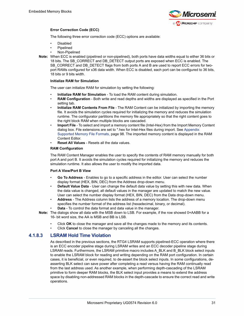
Embedded Memory Blocks
Error Correction Code (ECC)
The following three error correction code (ECC) options are available:
• Disabled• Pipelined• Non-Pipelined
Note: When ECC is enabled (pipelined or non-pipelined), both ports have data widths equal to either 36 bits or 18 bits. The SB_CORRECT and DB_DETECT output ports are exposed when ECC is enabled. The SB_CORRECT and DB_DETECT flags from both ports A and B are used to report ECC errors for two-port RAMs configured for x36 data width. When ECC is disabled, each port can be configured to 36 bits, 18 bits or 9 bits width.
Initialize RAM for Simulation
The user can initialize RAM for simulation by setting the following:
• Initialize RAM for Simulation - To load the RAM content during simulation.• RAM Configuration - Both write and read depths and widths are displayed as specified in the Port
setting tab.• Initialize RAM Contents From File - The RAM Content can be initialized by importing the memory
file. It avoids the simulation cycles required for initializing the memory and reduces the simulation runtime. The configurator partitions the memory file appropriately so that the right content goes to the right block RAM when multiple blocks are cascaded.
• Import File - To select and import a memory content file (Intel-Hex) from the Import Memory Content dialog box. File extensions are set to *.hex for Intel-Hex files during import. See Appendix: Supported Memory File Formats, page 98. The imported memory content is displayed in the RAM Content Editor.
• Reset All Values - Resets all the data values.RAM Configuration
The RAM Content Manager enables the user to specify the contents of RAM memory manually for both port A and port B. It avoids the simulation cycles required for initializing the memory and reduces the simulation runtime. It also allows the user to modify the imported data.
Port A View/Port B View
• Go To Address - Enables to go to a specific address in the editor. User can select the number display format (HEX, BIN, DEC) from the Address drop-down menu.
• Default Value Data - User can change the default data value by setting this with new data. When the data value is changed, all default values in the manager are updated to match the new value. User can select the number display format (HEX, BIN, DEC) from the Data drop-down menu.
• Address - The Address column lists the address of a memory location. The drop-down menu specifies the number format of the address list (hexadecimal, binary, or decimal).
• Data - To control the data format and data value in the manager. Note: The dialogs show all data with the MSB down to LSB. For example, if the row showed 0×AABB for a
16- bit word size, the AA is MSB and BB is LSB.
• Click OK to close the manager and save all the changes made to the memory and its contents.• Click Cancel to close the manager by canceling all the changes.
4.1.8.3 LSRAM Hold Time ViolationAs described in the previous sections, the RTG4 LSRAM supports pipelined-ECC operation where there is an ECC encoder pipeline stage during LSRAM writes and an ECC decoder pipeline stage during LSRAM reads. Furthermore, the LSRAM primitive macro includes A_BLK and B_BLK block select inputs to enable the LSRAM block for reading and writing depending on the RAM port configuration. In certain cases, it is beneficial, or even required, to de-assert the block select inputs. In some configurations, de-asserting BLK select can save power after completing a read versus having the RAM continually read from the last address used. As another example, when performing depth-cascading of the LSRAM primitive to form deeper RAM blocks, the BLK select input provides a means to extend the address space by disabling non-addressed RAM blocks in the depth-cascade to ensure the correct read and write operations.
Microsemi Proprietary UG0574 Revision 6.0 31

Embedded Memory Blocks
Designs which combine pipelined-ECC LSRAM mode with application use-models that could de-assert the BLK select inputs on a port used for LSRAM reads are recommended to use the LSRAM configurator cores described in the previous sections to create the LSRAM component instance. As described in RTG4 Customer Advisory Notice, CAN19011.1, the LSRAM primitive has an internal hold-time issue affecting the ECC decoder pipeline register during an LSRAM read, whenever the BLK select input for the port being read is de-asserted immediately after issuing the read operation.
When the BLK select input is de-asserted after issuing an LSRAM read, the LSRAM read DOUT port should go to zero after the appropriate number of clock cycles, depending on the number of LSRAM pipeline registers enabled (ECC pipeline and DOUT pipeline). Inside the LSRAM, de-asserting the BLK select clears the RAM data output latch which feeds the ECC decoder register and DOUT pipeline register, when enabled, or directly feeds the DOUT port when pipeline options are disabled.
In the case of pipelined-ECC mode, the BLK select de-assertion clears the RAM output data latch too quickly, violating the ECC decoder pipeline register's data hold time, preventing of the capture of the valid read data from the previously issued RAM read. The ECC decoder register captures the zeroed-out data, which causes all-zero data to shoot-through to the LSRAM DOUT port. Since the data is all-zero, the ECC is no longer correct, and the ECC output flags also assert. The issue is depicted in the figure below:
Figure 21 • LSRAM Pipelined-ECC BLK Select De-assertion Hold Time Violation After Read
This issue only impacts RTG4 two-port and dual-port LSRAM in pipelined-ECC mode.
This issue does NOT impact the following LSRAM configurations:
• Any configuration where the BLK select inputs are tied high• Non-pipelined-ECC mode (with or without DOUT pipeline)• Non-ECC mode (with or without DOUT pipeline)• Two-port LSRAM configurator component without depth-cascading• Dual-port LSRAM configurator component without depth cascading, and without exposing BLK
select input on any port used for reading• LSRAM port used exclusively for writes (There is no issue if BLK select input is de-asserted on that
port after a write command is issued)• Synplify-inferred LSRAM (Synplify Pro does not infer pipelined-ECC mode)The RTG4 two-port and dual-port LSRAM configurator cores in Libero SoC generate an additional fabric logic circuit for pipelined-ECC mode. The additional circuit avoids the hold time issue by delaying BLK select de-assertion to each LSRAM block.
The additional fabric logic generated by the configurator is shown in the following figure:
Microsemi Proprietary UG0574 Revision 6.0 32

Embedded Memory Blocks
Figure 22 • LSRAM Configurator Fabric Wrapper Logic Mitigating BLK De-assertion Hold Time Issue on Depth Cascaded LSRAM Component
Figure 22 shows an added AND (x3) and OR (x1) gates for depth cascaded RAMs working together with a pipelined version of the BLK select input. To prevent zeros from shooting through to read DOUT port, a pipelined version of the BLK select input + OR_0 keeps the BLK select input to the LSRAM primitive asserted 1 cycle longer, to delay BLK de-assertion during read. Furthermore, AND_2/AND_3 gate WEN/REN, respectively, with the non-registered BLK select input to prevent extra write/read commands due to the delayed BLK de-assertion at the LSRAM primitive BLK input port. Finally, AND_1, and similarly AND_0, ensures outputs and ECC flags are gated-off when not in the active read output cycle with correct pipeline latency depending on the number of pipeline stages active.
Note: With this LSRAM configurator update, single-depth dual-port LSRAM components which enable the use of the BLK select input will no longer hold the most recent read data after de-asserting REN. Read data output is gated by the pipelined BLK select input, and thus the RAM component will output zero an appropriate number of cycles after outputting the valid read data.
Therefore, it is recommended that designers generate pipelined-ECC LSRAM components using the Libero SoC configurator cores in Libero SoC v11.9 SP3 or above. Designers who manually instantiate pipelined-ECC LSRAM primitive macros would need to carefully consider whether the issue above applies to their application use-model, and manually add mitigation logic.
Lastly, designers are reminded to re-run static timing analysis in SmartTime using the appropriate timing constraints to ensure the additional fabric logic added to mitigate the issue works with the application's target clock frequency.
Microsemi Proprietary UG0574 Revision 6.0 33
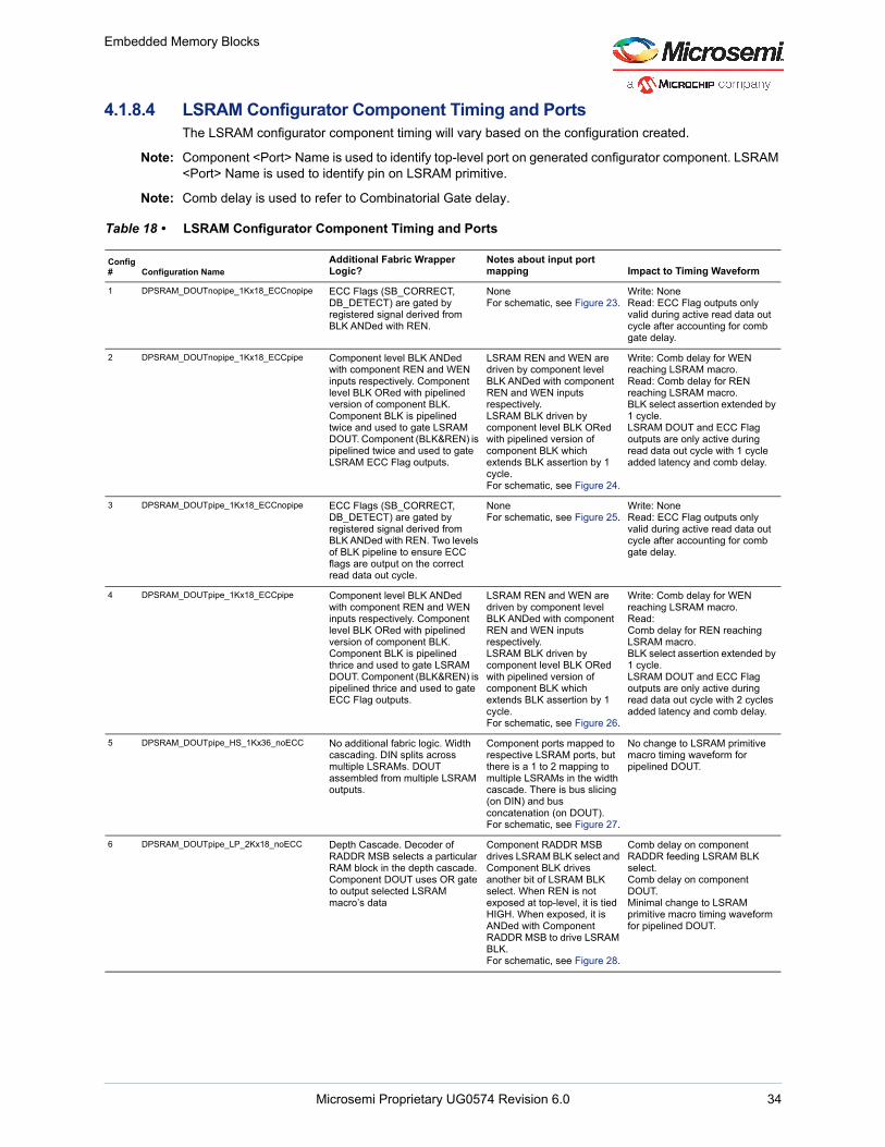
Embedded Memory Blocks
4.1.8.4 LSRAM Configurator Component Timing and PortsThe LSRAM configurator component timing will vary based on the configuration created.
Note: Component <Port> Name is used to identify top-level port on generated configurator component. LSRAM <Port> Name is used to identify pin on LSRAM primitive.
Note: Comb delay is used to refer to Combinatorial Gate delay.
Table 18 • LSRAM Configurator Component Timing and Ports
Config # Configuration Name
Additional Fabric Wrapper Logic?
Notes about input port mapping Impact to Timing Waveform
1 DPSRAM_DOUTnopipe_1Kx18_ECCnopipe ECC Flags (SB_CORRECT, DB_DETECT) are gated by registered signal derived from BLK ANDed with REN.
None For schematic, see Figure 23.
Write: NoneRead: ECC Flag outputs only valid during active read data out cycle after accounting for comb gate delay.
2 DPSRAM_DOUTnopipe_1Kx18_ECCpipe Component level BLK ANDed with component REN and WEN inputs respectively. Component level BLK ORed with pipelined version of component BLK. Component BLK is pipelined twice and used to gate LSRAM DOUT. Component (BLK&REN) is pipelined twice and used to gate LSRAM ECC Flag outputs.
LSRAM REN and WEN are driven by component level BLK ANDed with component REN and WEN inputs respectively.LSRAM BLK driven by component level BLK ORed with pipelined version of component BLK which extends BLK assertion by 1 cycle.For schematic, see Figure 24.
Write: Comb delay for WEN reaching LSRAM macro.Read: Comb delay for REN reaching LSRAM macro.BLK select assertion extended by 1 cycle.LSRAM DOUT and ECC Flag outputs are only active during read data out cycle with 1 cycle added latency and comb delay.
3 DPSRAM_DOUTpipe_1Kx18_ECCnopipe ECC Flags (SB_CORRECT, DB_DETECT) are gated by registered signal derived from BLK ANDed with REN. Two levels of BLK pipeline to ensure ECC flags are output on the correct read data out cycle.
NoneFor schematic, see Figure 25.
Write: NoneRead: ECC Flag outputs only valid during active read data out cycle after accounting for comb gate delay.
4 DPSRAM_DOUTpipe_1Kx18_ECCpipe Component level BLK ANDed with component REN and WEN inputs respectively. Component level BLK ORed with pipelined version of component BLK. Component BLK is pipelined thrice and used to gate LSRAM DOUT. Component (BLK&REN) is pipelined thrice and used to gate ECC Flag outputs.
LSRAM REN and WEN are driven by component level BLK ANDed with component REN and WEN inputs respectively.LSRAM BLK driven by component level BLK ORed with pipelined version of component BLK which extends BLK assertion by 1 cycle.For schematic, see Figure 26.
Write: Comb delay for WEN reaching LSRAM macro.Read:Comb delay for REN reaching LSRAM macro.BLK select assertion extended by 1 cycle.LSRAM DOUT and ECC Flag outputs are only active during read data out cycle with 2 cycles added latency and comb delay.
5 DPSRAM_DOUTpipe_HS_1Kx36_noECC No additional fabric logic. Width cascading. DIN splits across multiple LSRAMs. DOUT assembled from multiple LSRAM outputs.
Component ports mapped to respective LSRAM ports, but there is a 1 to 2 mapping to multiple LSRAMs in the width cascade. There is bus slicing (on DIN) and bus concatenation (on DOUT).For schematic, see Figure 27.
No change to LSRAM primitive macro timing waveform for pipelined DOUT.
6 DPSRAM_DOUTpipe_LP_2Kx18_noECC Depth Cascade. Decoder of RADDR MSB selects a particular RAM block in the depth cascade. Component DOUT uses OR gate to output selected LSRAM macro’s data
Component RADDR MSB drives LSRAM BLK select and Component BLK drives another bit of LSRAM BLK select. When REN is not exposed at top-level, it is tied HIGH. When exposed, it is ANDed with Component RADDR MSB to drive LSRAM BLK.For schematic, see Figure 28.
Comb delay on component RADDR feeding LSRAM BLK select.Comb delay on component DOUT.Minimal change to LSRAM primitive macro timing waveform for pipelined DOUT.
Microsemi Proprietary UG0574 Revision 6.0 34

Embedded Memory Blocks
The following schematic diagrams depict 12 configurations supported by the LSRAM which are mentioned in the preceding table:
7 TPSRAM_DOUTnopipe_512x36_ECCnopipe Component REN is pipelined and used to gate off each port’s ECC flag outputs which are OR’d together to make one DB_DETECT and one SB_CORRECT output.
Component level WEN drives LSRAM Write Port BLK select input. LSRAM WEN tied HIGH.For schematic, see Figure 29.
Minimal change from LSRAM primitive timing for non-pipelined ECC.Comb delay on ECC flag outputs (AND + OR delay)ECC Flag outputs only valid during active read data out cycle.
8 TPSRAM_DOUTnopipe_512x36_ECCpipe Component REN is pipelined twice and used to gate off each port’s ECC flag outputs which are OR’d together to make one DB_DETECT and one SB_CORRECT output.
Component REN drives LSRAM read port REN.LSRAM Read Port BLK is tied HIGH.Component level WEN drives LSRAM Write Port BLK select input. LSRAM WEN tied HIGH.For schematic, see Figure 30.
Minimal change from LSRAM primitive timing with pipelined ECC. Comb delay on ECC flag outputs (AND + OR delay). ECC Flag outputs only valid during active read data out cycle.
9 TPSRAM_DOUTpipe_512x36_ECCnopipe Component REN is pipelined twice and used to gate off each port’s ECC flag outputs which are OR’d together to make one DB_DETECT and one SB_CORRECT output.
Component REN drives LSRAM read port REN.LSRAM Read Port BLK is tied HIGH.Component level WEN drives LSRAM Write Port BLK select input. LSRAM WEN tied HIGH.For schematic, see Figure 31.
Minimal change from LSRAM primitive timing with only DOUT pipeline. Comb delay on ECC flag outputs (AND + OR delay). ECC Flag outputs only valid during active read data out cycle.
10 TPSRAM_DOUTpipe_512x36_ECCpipe Component REN is pipelined three times and used to gate off each port’s ECC flag outputs which are OR’d together to make one DB_DETECT and one SB_CORRECT output.
Component REN drives LSRAM read port REN.LSRAM Read Port BLK is tied HIGH.Component level WEN drives LSRAM Write Port BLK select input. LSRAM WEN tied HIGH.For schematic, see Figure 32.
Minimal change from LSRAM primitive timing for pipelined-ECC with DOUT pipeline. Comb delay on ECC flag outputs (AND + OR delay). ECC Flag outputs only valid during active read data out cycle.
11 TPSRAM_DOUTpipe_HS_512x72_noECC No additional fabric logic. Width cascading. DIN splits across multiple ports and multiple LSRAMs. DOUT assembled from all DOUT ports of multiple LSRAMs macros.
Component ports mapped to respective LSRAM. There is bus slicing on component DIN across both LSRAM ports and both LSRAM macros. There is bus concatenation from both DOUT ports of both LSRAM macros.For schematic, see Figure 33.
No change to LSRAM primitive macro timing waveform for pipelined DOUT.
12 TPSRAM_DOUTpipe_LP_1Kx36_noECC Depth Cascade. Decoder of RADDR MSB selects a particular RAM block in the depth cascade. Component DOUT uses OR gate to output selected LSRAM macro’s data.
Component RADDR and WADDR MSB each drives a bit of LSRAM read and write port’s BLK select, respectively. Component REN drives another bit of LSRAM read port BLK select. Component WEN drives another bit of LSRAM write port BLK select. LSRAM REN inputs tied HIGH. LSRAM WEN inputs tied HIGH.For schematic, see Figure 34.
Comb delay on component RADDR/WADDR feeding LSRAM BLK select. Comb delay on component DOUT. Minimal change to LSRAM primitive macro timing waveform for pipelined DOUT.
Table 18 • LSRAM Configurator Component Timing and Ports
Config # Configuration Name
Additional Fabric Wrapper Logic?
Notes about input port mapping Impact to Timing Waveform
Microsemi Proprietary UG0574 Revision 6.0 35
Embedded Memory Blocks
Figure 23 • DPSRAM_DOUTnopipe_1Kx18_ECCnopipe
Figure 24 • DPSRAM_DOUTnopipe_1Kx18_ECCpipe
Microsemi Proprietary UG0574 Revision 6.0 36

Embedded Memory Blocks
Figure 25 • DPSRAM_DOUTpipe_1Kx18_ECCnopipe
Figure 26 • DPSRAM_DOUTpipe_1Kx18_ECCpipe
Microsemi Proprietary UG0574 Revision 6.0 37

Embedded Memory Blocks
Figure 27 • DPSRAM_DOUTpipe_HS_1Kx36_noECC
Figure 28 • DPSRAM_DOUTpipe_LP_2Kx18_noECC
Microsemi Proprietary UG0574 Revision 6.0 38

Embedded Memory Blocks
Figure 29 • TPSRAM_DOUTnopipe_512x36_ECCnopipe
Figure 30 • TPSRAM_DOUTnopipe_512x36_ECCpipe
Microsemi Proprietary UG0574 Revision 6.0 39

Embedded Memory Blocks
Figure 31 • TPSRAM_DOUTpipe_512x36_ECCnopipe
Figure 32 • TPSRAM_DOUTpipe_512x36_ECCpipe
Microsemi Proprietary UG0574 Revision 6.0 40

Embedded Memory Blocks
Figure 33 • TPSRAM_DOUTpipe_HS_512x72_noECC
Figure 34 • TPSRAM_DOUTpipe_LP_1Kx36_noECC
Microsemi Proprietary UG0574 Revision 6.0 41
Embedded Memory Blocks
4.1.8.4.1 Functional Timing WaveformsThe following table maps each timing waveform to all the applicable configuration options.
Table 19 • Functional Timing Waveforms
FigureLSRAM Configurator Use-Case
Depicted Difference vs LSRAM Primitive TimingCase A: LSRAM Configurator with
Comb Delay. Gating ECC Flag Outputs, non-Pipelined ECC.
For functional timing waveform, see Figure 35.
Config #1, Config #3, Config #7, Config #9
Combinatorial Delay on ECC Flag Outputs. ECC Flag Outputs are Gated Off when not
in valid read data out cycle.
Case B: LSRAM Read Operation, Pipelined Read without ECC.
For functional timing waveform, see Figure 36.
Config #5 and Config #11 No change to LSRAM primitive macro timing waveform for pipelined DOUT, no
ECC.
Case C: Depth Cascaded Dual Port LSRAM Component, Pipelined
Read without ECC.For functional timing waveform, see
Figure 37.
Config #6 Combinatorial Delay on BLK Select @ LSRAM Block, Combinatorial Delay on
DOUT.
Case D: Depth Cascaded Two Port LSRAM Component, Pipelined
Read without ECC.For functional timing waveform, see
Figure 38.
Config #12 Combinatorial Delay on BLK Select @ LSRAM Block, Combinatorial Delay on
DOUT.
Case E: Dual Port LSRAM with Pipelined ECC.
For functional timing waveform, see Figure 39.
Config #2 and Config #4 Write: Comb delay for WEN reaching LSRAM macro.
Read: Comb delay for REN reaching LSRAM macro.
BLK select assertion extended by 1 cycle.LSRAM DOUT and ECC Flag outputs are only active during respective read data out
cycle.
Case F: Two Port LSRAM with Pipelined ECC.
For functional timing waveform, see Figure 40.
Config #8 and Config #10 Minimal change from LSRAM primitive timing for pipelined-ECC with and without
DOUT pipeline. Some comb delay on ECC flag outputs (AND + OR delay). ECC Flag outputs only valid during active read data
out cycle.
Microsemi Proprietary UG0574 Revision 6.0 42

Embedded Memory Blocks
Figure 35 • Case A: LSRAM Configurator Component with Comb Delay Gating ECC Flag Outputs, non-Pipelined ECC
A_ADDR[10:0]B_ADDR[10:0]
A_BLK[2:0]B_BLK[2:0]
A_DOUT[17:0] B_DOUT[17:0]
A_DOUT[17:0] B_DOUT[17:0]
Non-pipeline mode With Non-pipelined ECC
A0 A1 A2
D(A0) D(A1)
D(A0)
Pipelined access with non-pipelined ECC
SB_CORRECTDB_DETECT
SB_CORRECT DB_CORRECT
Corresponding ECC flag outputs
Combinational Gate Delay since ECC Outputs are gated by registered (BLK & REN) signal to ensure flag outputs are valid on read data out cycle.
Corresponding ECC flag outputs
Combinational Gate Delay since ECC Outputs are gated by registered (BLK & REN) signal to ensure flag outputs are valid on
read data out cycle.
A_CLKB_CLK
Clock Cycle #1 Clock Cycle #2
A_WEN[1:0]B_WEN[1:0]
A_RENB_REN
D(A1)
D(A2)
A3
D(A2)
Clock Cycle #3
Microsemi Proprietary UG0574 Revision 6.0 43

Embedded Memory Blocks
Figure 36 • Case B: LSRAM Read Operation, Pipelined Read without ECC
Figure 37 • Case C: Depth Cascaded Dual Port LSRAM Component, Pipelined Read without ECC
A_ADDR[10:0]B_ADDR[10:0]
A_BLK[2:0]B_BLK[2:0]
A_DOUT[17:0] B_DOUT[17:0]
Pipelined access without ECC
A0 A1 A2
D(A2)D(A0)
Data in Address A0
A3
D(A1)
A_CLKB_CLK
Clock Cycle #1 Clock Cycle #2 Clock Cycle #3
A_WEN[1:0]B_WEN[1:0]
A_RENB_REN
A_ADDR[10:0]B_ADDR[10:0]
A_BLK[2:0]B_BLK[2:0]
A_DOUT[17:0] B_DOUT[17:0]
A0 A1 A2
D(A2)D(A0)
Pipelined Access without ECC
Dual Port LSRAM Catlog Core Component Timing Waveform:Depth Cascaded, Pipelined Read without ECC
Optional Port
Combinational Delay
A3
D(A1)
A_CLKB_CLK
A_WEN[1:0]B_WEN[1:0]
A_RENB_REN
A_BLK[2:0]B_BLK[2:0]
@LSRAM Block
Clock Cycle #1 Clock Cycle #2 Clock Cycle #3
Microsemi Proprietary UG0574 Revision 6.0 44

Embedded Memory Blocks
Figure 38 • Case D: Depth Cascaded Two Port LSRAM Component, Pipelined Read without ECC
RADDR[10:0]WADDR[10:0]
RD[35:0]
A0 A1 A2
D(A2)D(A0)
Pipelined Access without ECC
Two Port LSRAM Catlog Core Component Timing Waveform:Depth Cascaded, Pipelined Read without ECC
Combinational Delay
A3
D(A1)
RCLKWCLK
B_WEN[1:0]
A_REN
A_BLK[2:0]B_BLK[2:0]
@LSRAM Block
Clock Cycle #1 Clock Cycle #2 Clock Cycle #3
Microsemi Proprietary UG0574 Revision 6.0 45

Embedded Memory Blocks
Figure 39 • Case E: Dual Port LSRAM with Pipelined ECC
A_CLKB_CLK
A_ADDR[10:0]B_ADDR[10:0] A0
Clock Cycle #1 Clock Cycle #2
A_DOUT[17:0] B_DOUT[17:0]
Non-Pipelined Read with Pipelined ECC
D(A0)=Data in Address A0
SB_CORRECTDB_DETECT
Corresponding ECC Flag Outputs
A_DIN[17:0]B_DIN[17:0]
1.For cases where pipelined ECC mode is used, the first write cycle is used by the ECC encoder and the second clock cycle is used when the LSRAM memory array is actually written. Therefore, it is not legal to perform a write immediately followed by a read to the same address on the next clock cycle, because LSRAM is being written with the newly encoded data. When using pipelined ECC mode, after issuing a write to a given LSRAM address, a subsequent read to that address must wait until two clock cycles later to ensure the correct data is being read. Once the read command is issued, pipelined ECC mode requires one clock cycle to decode the data from LSRAM before it is presented on the data output port.
A_WEN[1:0]B_WEN[1:0]
D0
A_RENB_REN
D(A0) D(A0)
A_DOUT[17:0] B_DOUT[17:0]
Pipelined Read with ECC Pipelined
SB_CORRECTDB_DETECT
Corresponding ECC Flag Outputs
D(A0) D(A0)
A1
Clock Cycle #3 Clock Cycle #4
A2
3'b111 3'b111A_BLK[2:0]B_BLK[2:0]
Read Enable during Pipelined ECC
3'b111 3'b111A_BLK[2:0]B_BLK[2:0]
@LSRAM Block Input
A_WEN[1:0]B_WEN[1:0]
@LSRAM Block Input
A_RENB_REN
@LSRAM Block Input
Combinational Delay Combinational Delay
Combinational Delay Combinational Delay
Microsemi Proprietary UG0574 Revision 6.0 46

Embedded Memory Blocks
Figure 40 • Case F: Two Port LSRAM with Pipelined ECC
4.1.8.5 Simulating ECC Errors in LSRAMThe simulation models for the LSRAM and µSRAM support two signals, the SB_CORRECT signal to indicate a single-bit ECC error has occurred and the DB_DETECT signal to indicate that a double-bit, non-correctable error has occurred. The signals are asserted in conjunction with each other to pass this information. The read data is unaffected by the flag behavior and will always be correct in the simulation regardless of the flag state.
The added logic also ensures the flag outputs from the RAM block are always assigned a value and do not become unknown during periods when the read enable is not asserted high. For more information, see Libero SoC v11.9 SP2, v11.9 SP3, or Libero SoC v12.1 release notes.
The following figure shows the instantiations and connection of the memories along with the exposed ECC flag signals. The RTG4TPSRAM and RTG4URAM are configured for ECC in the non-pipelined mode.
Enable the simulation to report errors, the following options must be added to the vsim command. These are set on the command line when entering the vsim command or through the Libero Project settings as shown in the following figure.
Table 20 • ECC Errors Flag
ECC Error Flag SB_CORRECT DB_DETECTNo Error 0 0
Single-bit Error Corrected 1 0
Double-bit Error 1 1
RCLKWCLK
RADDR[10:0]WADDR[10:0] A0
Clock Cycle #1 Clock Cycle #2
Corresponding ECC Flag Outputs
Non-Pipelined Read with Pipelined ECC
D(A0)=Data in Address A0
SB_CORRECTDB_DETECT
Corresponding ECC Flag Outputs
WD[35:0]
1.For cases where pipelined ECC mode is used, the first write cycle is used by the ECC encoder and the second clock cycle is used when the LSRAM memory array is actually written. Therefore, it is not legal to perform a write immediately followed by a read to the same address on the next clock cycle, because LSRAM is being written with the newly encoded data. When using pipelined ECC mode, after issuing a write to a given LSRAM address, a subsequent read to that address must wait until two clock cycles later to ensure the correct data is being read. Once the read command is issued, pipelined ECC mode requires one clock cycle to decode the data from LSRAM before it is presented on the data output port.
B_WEN[1:0]
D0
A_REN
D(A0)
D(A0)
Pipelined Read with ECC Pipelined
SB_CORRECTDB_DETECT
A1
Clock Cycle #3 Clock Cycle #4
A2
Read Enable during Pipelined ECC
RD[35:0]
RD[35:0]
Combinational Delay
Microsemi Proprietary UG0574 Revision 6.0 47

Embedded Memory Blocks
Figure 41 • Libero Project Settings
-gERROR_PROBABILITY
Legal values are - 0 <= value <= 1
The simulation uses a random number generator and compares its value with the value assigned to ERROR_PROBABILITY
SB_CORRECT asserted = ‘1’ indicates a single bit error has occurred.
The assertion rate of SB_CORRECT is directly related to the value of ERROR_PROBABILITY
Increasing the value results in SB_CORRECT being asserted more often.
Decreasing the value results in SB_CORRECT being asserted less often.
-gCORRECTION_PROBABILITY
Legal values are - 0 <= value <= 1
The simulation uses a random number generator and compares its value with the value assigned to
DB_DETECT asserted = ‘1’ indicates more than one bit errors have occurred and could not be corrected.
ERROR_CORRECTION
The assertion rate of DB_DETECT is inversely related to the value of CORRECTION_PROBABILITY
Increasing the value results in DB_DETECT being asserted less often.
Decreasing the value results in DB_DETECT being asserted more often.
4.1.8.5.1 TPSRAM WaveformsThe following waveform was captured with the settings of 0.5 for both ERROR_PROBABILITY and CORRECTION_PROBABILITY. It can be seen that SB_CORRECT signal is high except for one clock during the read period indicating single bit errors were occurring during this time period. The state of DB_DETECT during the same period indicates if these were single bit errors (DB_DETECT = '0') or double bit errors (DB_DETECT = '1').
Figure 42 • TPSRAM: 0.5 Error Probability and 0.5 Correction Probability
The following waveform was captured with the settings of 0.25 for ERROR_PROBABILITY and 0.85 for CORRECTION_PROBABILITY. The new values should cause fewer errors to be asserted on SB_CORRECT and less double bit errors asserted on DB_DETECT. From the following waveform, it can
Microsemi Proprietary UG0574 Revision 6.0 48

Embedded Memory Blocks
be seen there are fewer errors signaled by the SB_CORRECT signal and fewer (none) signaled by the DB_DETECT signal than in the previous waveform.
Figure 43 • TPSRAM: 0.25 Error Probability and 0.85 Correction Probability
The following waveform was captured with the settings of 0.15 for both ERROR_PROBABILITY and CORRECTION_PROBABILITY. The new values should cause fewer errors to be asserted on SB_CORRECT and more double bit errors asserted on DB_DETECT. From the following waveform, it can be seen there are fewer errors signaled by the SB_CORRECT signal and more signaled by the DB_DETECT signal than in the previous waveform.
Figure 44 • TPSRAM: 0.15 Error Probability and 0.15 Correction Probability
4.1.9 Use Model: LSRAM Write-Feed-Through using Fabric LogicThe RTG4 LSRAM supports the write-feed-through operation using the fabric logic. The following figure shows the example implementation of write-feed-through fabric logic. The fabric logic consists of extra pipeline registers to match the LSRAM pipeline mode and MUX logic to select write-feed-through operation.
Figure 45 • Sample Write-Feed-Thorough Fabric Logic
module lsram_wft (clk,we,addr,d,fl_wf,q);
D Q D Q
LSRAM dout
1
0
din
we
q
we
clk
d
fl_wf
Registers as needed to match LSRAM pipeline modes
Microsemi Proprietary UG0574 Revision 6.0 49

Embedded Memory Blocks
input [7:0] d;input [9:0] addr;input clk, we;input fl_wf;reg [9:0] addr_reg;output [7:0] q;reg [7:0] mem [1023:0] ;reg [7:0] dout;reg [7:0] dreg;always @ (posedge clk )begin dreg <= d;endalways @(posedge clk) begin addr_reg <= addr; if(we) mem[addr] <= d;endalways @ (posedge clk )begin dout <= mem[addr_reg];endassign q = (fl_wf && we) ? dreg : dout; endmodule
Figure 46 • Write-Feed-Through using Fabric Logic - RTL Schematic View
Microsemi Proprietary UG0574 Revision 6.0 50
Embedded Memory Blocks
4.1.10 Debugging LSRAMs Using SmartDebugRTG4 LSRAM blocks support real-time memory debug using the SmartDebug software. However, depending on the design running in the RTG4 fabric, a debug session using SmartDebug memory debug can inadvertently write incorrect data into the LSRAM being debugged. For example, if the user design has the LSRAM block select (A_BLK[2:0], B_BLK[2:0]) and write enable (A_WEN[1:0], B_WEN[1:0]) inputs enabled when the SmartDebug memory access occurs, the instantaneous transition between user access and SmartDebug access to the LSRAM could result in unintentional writes to the LSRAM. To prevent this undesirable scenario, a manual handshake technique can be employed such that the user logic in the fabric can disable the block select and write enable inputs to the LSRAM before performing a SmartDebug memory debug access. Implementing the manual handshake described below to prevent SmartDebug corruption of the LSRAM being accessed requires HDL modifications to add a gate in the path of the block select and write enable control signals. Therefore, this can negatively impact the timing of the user block select and write enable inputs to the LSRAM. This timing impact must be analyzed during static timing analysis using SmartTime. Although the LSRAM primitive macro contains a BUSY output signal to indicate when an access is occurring, that signal asserts when a memory access starts. To prevent this unintentional write, a signal which transitions before the switch from user access to SmartDebug access must be created. Therefore, the BUSY output would transition too late to prevent this scenario in all cases.
Instead of using the BUSY output, the user can create a manual handshake signal by using a flip-flop whose value can be manually changed using SmartDebug active probe writes. This flip-flop output can be used to gate A_BLK, B_BLK, A_WEN, and B_WEN inputs to the LSRAM by modifying the user HDL. When the user is ready to perform a SmartDebug memory access, they must first use the Active Probe interface in SmartDebug, select the flip-flop which gates the control signals to the RAM they plan to debug, and write a logic-1 into the flip-flop. This disables the fabric block select and write enable to the LSRAM. Once fabric write access to the LSRAM is disabled the user can switch to the SmartDebug Memory Debug tab to perform the memory accesses. After the memory debug is complete, another active probe write is required to set the handshake flip-flop to logic-0, thus re-enabling fabric writes to the LSRAM. The example HDL below shows a module which can be added to the user design, and instantiated once per design or once per logical memory instance to create the handshake signal. Note that there are specific synthesis directives applied to prevent the active_probe_latch SLE from being optimized away during synthesis. The HDL below specifies that the active_probe_latch SLE must be reset to logic-0 during design reset to ensure that the LSRAM write ports are accessible to the user design by default. The RTG4 embedded power-on-reset signal distributed to the SLE ALn input automatically resets the active_probe_latch flip-flop because the code below maps the ADn input to a logic-1. For more information about the SLE_RT truth table, refer to the RTG4 Macro Library Guide (https://www.microsemi.com/document-portal/doc_download/1243102-rtg4-macro-library-guide-with-libero-soc-v11-9-release).
module probeWrite ( RESET_N_IN,PRBWR_IN, ENABLE_HNDSHAKE, HNDSHAKE_OUT ) /* synthesis syn_hier = "hard" */;
input RESET_N_IN; input PRBWR_IN; input ENABLE_HNDSHAKE; output HNDSHAKE_OUT;
reg active_probe_latch /*synthesis syn_preserve = 1*/; wire dummyClk /*synthesis syn_keep=1*/;// This latch is to be driven asynchronously by Active Probe Write to 1 or 0
Microsemi Proprietary UG0574 Revision 6.0 51

Embedded Memory Blocks
always @(posedge dummyClk or negedge RESET_N_IN) beginif (!RESET_N_IN)active_probe_latch <= 1'b0;else active_probe_latch <= PRBWR_IN; endassign HNDSHAKE_OUT = active_probe_latch & ENABLE_HNDSHAKE;endmoduleThe post-compile netlist view of the active_probe_latch is shown in the following figure:
Figure 47 • Post-Compile Netlist View of active_probe_latch
When instantiating the probeWrite_1 module, the PRBWR_IN input to the active_probe_latch must be statically tied LOW since the writes to this SLE will be driven by SmartDebug Active Probe writes. The HNDSHAKE_OUT signal will only propagate to user logic if the ENABLE_HNDSHAKE input is HIGH. This provides control to enable or disable debug in the design, if required. For example, during design development, it would make sense to tie the ENABLE_HNDSHAKE input HIGH. Once the design is finalized, and debug is no longer required, the ENABLE_HNDSHAKE signal can be driven LOW to prevent the active_probe_latch output from gating-off user writes to the LSRAM. The following figure shows an example instantiation of this module.
Figure 48 • Instantiation of probeWrite_1 module with PRBWR_IN tied LOW
An instantiated LSRAM can be modified to use gated versions of A_BLK, B_BLK, A_WEN, and B_WEN:
wire A_BLK_gated, B_BLK_gated, A_WEN_gated, B_WEN_gated; wire EN_DEBUG; wire DEBUG_ACTIVE; assign A_BLK_gated = DEBUG_ACTIVE ? 1'b0 : A_BLK; assign B_BLK_gated = DEBUG_ACTIVE ? 1'b0 : B_BLK; assign A_WEN_gated = DEBUG_ACTIVE ? 1'b0 : A_WEN; assign B_WEN_gated = DEBUG_ACTIVE ? 1'b0 : B_WEN; probeWrite probeWrite_0( // Inputs
Microsemi Proprietary UG0574 Revision 6.0 52

Embedded Memory Blocks
.RESET_N_IN ( RESET_N ), .PRBWR_IN ( 1'b0 ), .ENABLE_HNDSHAKE ( EN_DEBUG ), // Outputs .HNDSHAKE_OUT ( DEBUG_ACTIVE ) );These gated versions of block select and write enable can then be mapped to the RAM macro block select and write enable ports:
RAM1K18_RT myDPRAM (
.A_BLK({A_BLK_gated, 1'b1, 1'b1}), .B_BLK({B_BLK_gated, 1'b1, 1'b1}), .A_WEN({A_WEN_gated, A_WEN_gated}), .B_WEN({B_WEN_gated, B_WEN_gated}),);
Note: Connect any 1 bit of A_BLK[2:0] and B_BLK[2:0] to a logic-0 to turn off that LSRAM port's block select input. The example above shows only 1 bit of the block select input driven by the gated version of A_BLK and B_BLK while the other 2 bits are tied to logic-1.
In contrast, the write enable input can be used on a per-byte basis in some RAM configurations, and thus both bits of A_WEN[1:0] and B_WEN[1:0] should be driven by the gated write enable signal.
The example above demonstrates how the manual handshake signal can be used to disable the write ports of an instantiated LSRAM. This concept can be directly applied to LSRAM blocks which have been manually instantiated in the user HDL.The Dual-port and Two-port Configurators can expose Write Byte Enables directly. In either case, the concept above can be used to disable the block select and write enable inputs to the individual RAM block instances during debug, while maintaining the generated component's port mapping to the individual block select and write enable inputs during normal user operation.
Once the LSRAM is setup to use the gated versions of block select and write enable, the user can employ the Active Probe write in SmartDebug to enable the handshake signal from the active_probe_latch and then perform Memory Debug on the LSRAM.
Microsemi Proprietary UG0574 Revision 6.0 53

Embedded Memory Blocks
Figure 49 • Writing a Logic-1 to the active_probe_latch Handshake Signal
Microsemi Proprietary UG0574 Revision 6.0 54

Embedded Memory Blocks
4.2 µSRAMEach µSRAM has two read ports and one write port for two-port memory requirements. The following figure shows the µSRAM diagram.
Figure 50 • Functional Block Diagram of µSRAM
The following table lists the ports available in µSRAM.
Table 21 • Port List for µSRAM
Port Name Pin Direction Type1 Polarity DescriptionPort AA_ADDR[6:0] Input Dynamic Port A read address
A_BLK[1:0] Input Dynamic Active high Port A block selects
A_WIDTH Input Static Port A depth × width mode selection
A_DOUT[17:0] Output Dynamic Port A read-data
A_DOUT_EN Input Dynamic Active high Port A read-data pipeline register enable
A_DOUT_BYPASS Input Static Active low Port A pipeline register select
A_DOUT_SRST_N Input Dynamic Active low Port A read-data pipeline register synchronous-reset
A_CLK Input Dynamic Rising edge Port A register clock
A_ADDR_EN Input Dynamic Active high Port A read-address register enable
A_ADDR_BYPASS Input Static Active low Port A read-address pipeline register select
A_ADDR_SRST_N Input Dynamic Active low Port A read-address register synchronous-reset
A_SB_CORRECT Output Dynamic Active high Port A 1-bit error correction flag
A_DB_DETECT Output Dynamic Active high Port A 2-bit error detection flag
Port ARead
Decode
Port BRead
Decode
Memory Array64 x 18
C_ADDR[6:0]
C_DIN[17:0]
C_WEN
C_CLK
Port
C w
rite
cont
rol +
EC
C lo
gic
A_ADDR[6:0]A_BLK[1:0]
A_CLK
B_ADDR[6:0]B_BLK[1:0]
B_CLK
A_ADDR_BYPASS
B_ADDR_BYPASS
C_BLK[1:0]
B_ADDR_EN
A_ADDR_EN
A_DOUT[17:0]
PipelineRegister
ECC_EN
B_DOUT[17:0]
ECCLogic
ECCLogic
A_DOUT_EN
ECC_EN
A_SB_CORRECT
A_DB_DETECT
B_SB_CORRECT
B_DB_DETECT
B_DOUT_EN
ECC_EN
PipelineRegister
Microsemi Proprietary UG0574 Revision 6.0 55

Embedded Memory Blocks
4.2.1 µSRAM Read OperationRead operations are independent of write operations and are performed asynchronously. Synchronous read operations can be performed by using fabric flip-flops as pipeline registers. These flip-flops are located in the associated interface logic at the read address input and read data output.
When the input address (R_ADDR[]) is provided, the output data is available on the output data bus after a read delay. When BLK_EN is high, the read operations are enabled. R_DATA contains the contents of the memory location selected by R_ADDR. When block select is low, the R_DATA is driven to zero.
Port BB_ADDR[6:0] Input Dynamic Port B read-address
B_BLK[1:0] Input Dynamic Active high Port B block selects
B_WIDTH Input Static Port B depth × width mode
B_DOUT[17:0] Output Dynamic Port B read-data
B_DOUT_EN Input Dynamic Active high Port B read-data pipeline register enable
B_DOUT_BYPASS Input Static Active low Port B read-data pipeline register select
B_DOUT_SRST_N Input Dynamic Active low Port B read-data pipeline register synchronous-reset
B_CLK Input Dynamic Rising edge Port B register clock
B_ADDR_EN Input Dynamic Active high Port B read-address register enable
B_ADDR_BYPASS Input Static Active low Port B read-address register select
B_ADDR_SRST_N Input Dynamic Active low Port B read-address register synchronous-reset
B_SB_CORRECT Output Dynamic Active high Port B 1-bit error correction flag
B_DB_DETECT Output Dynamic Active high Port B 2-bit error detection flag
Port CC_ADDR[6:0] Input Dynamic Port C write address
C_CLK Input Dynamic Rising edge Port C clock input
C_DIN[17:0] Input Dynamic Port C write-data
C_WEN Input Dynamic Active high Port C write-enable
C_BLK[1:0] Input Dynamic Active high Port C block selects
C_WIDTH Input Static Port C depth × width mode
Common SignalsARST_N Input Global Active low Read-address and read-data pipeline registers
asynchronous-reset
ECC_EN Input Static Active high Enable ECC
ECC_DOUT_BYPASS Input Static Active low ECC pipeline register select
DELEN Input Static Active high Enable SET mitigation
SECURITY Input Static Active high Lock access to system controller
BUSY Output Dynamic Active high Busy signal from system controller
1. Static inputs are defined at design time and must be tied to 0 or 1.
Table 21 • Port List for µSRAM (continued)
Port Name Pin Direction Type1 Polarity Description
Microsemi Proprietary UG0574 Revision 6.0 56

Embedded Memory Blocks
µSRAM blocks are read through two ports—port A and port B. There are four modes for read operations:
• Synchronous read mode without pipeline registers (Synchronous-Asynchronous mode)• Synchronous read mode with pipeline registers (Synchronous-Synchronous mode)• Asynchronous read mode without pipeline registers (Asynchronous-Asynchronous mode)• Asynchronous read mode with pipeline registers (Asynchronous-Synchronous mode)
4.2.1.1 µSRAM Synchronous Read OperationSynchronous read mode requires that the input registers for the address and block select inputs are configured in STMR-D flip-flop mode (A_ADDR_BYPASS or B_ADDR_BYPASS = 0). Similarly, on the output side, the pipeline registers can be configured as registered or asynchronous.
When the pipeline registers are enabled, the clock inputs of both the input and output registers must be synchronous to each other and fed with a single clock source. It is recommended to configure the registers as pipeline registers during read operation to avoid glitches on the read output data lines.
In Synchronous read mode, the address (A_ADDR or B_ADDR) and block select (A_BLK or B_BLK) inputs must satisfy the setup and hold timing with respect to the input clocks (A_ CLK or B_ CLK).
4.2.1.1.1 Synchronous Read Mode without Pipeline Registers (Synchronous-Asynchronous Read Mode)• The input registers are configured in synchronous read mode.• The output pipeline registers are configured as transparent.• This mode is achieved by configuring the following settings:
• A_DOUT_BYPASS = 1 or B_DOUT_BYPASS = 1• A_ADDR_BYPASS or B_ADDR_BYPASS = 0• A_DOUT_SRST_N = 1 or B_DOUT_SRST_N = 1• A_DOUT_EN or B_DOUT_EN = 1• A_BLK = 1, B_BLK = 1
• The output data is displayed immediately in the same clock cycle in which the address and block select inputs were registered.
• The µSRAM block can generate glitches on the output buses when used without the pipeline registers.
The following figure shows the timing waveforms for synchronous-asynchronous read operation without pipeline registers.
Figure 51 • Synchronous-Asynchronous Read Operation without Pipeline Registers
`
A_CLKB_CLK
A_ADDR[6:0]B_ADDR[6:0]
A_BLKB_BLK
A_DOUT[17:0]B_DOUT[17:0]
A0 A1 A2
Output in the synchronous – asynchronous mode without ECC registers
D0
A_DOUT[17:0]B_DOUT[17:0]
Output in the synchronous – asynchronous mode with ECC registers
D0D-1
D-1
D-2
D2
Microsemi Proprietary UG0574 Revision 6.0 57

Embedded Memory Blocks
4.2.1.1.2 Synchronous Read Mode with Pipeline Registers (Synchronous-Synchronous Read Mode)• The input registers are configured in synchronous read mode.• The output pipeline registers are configured as edge-triggered registers (Pipelined mode).• Pipelined mode is achieved by making the following settings:
• A_DOUT_BYPASS or B_DOUT_BYPASS = 0• A_ADDR_BYPASS or B_ADDR_BYPASS = 0• A_DOUT_SRST_N = 1 or B_DOUT_SRST_N = 1• A_DOUT_EN or B_DOUT_EN = 1• A_BLK = 1, B_BLK = 1
• The input register clock and pipeline register clock must be synchronous to each other; hence they must be sourced from the same clock input.
• The output data appears on the output bus in the next clock cycle.The following figure shows the timing waveforms for synchronous-synchronous read operation with pipeline registers.
Figure 52 • Synchronous-Synchronous Read Operation with Pipeline Registers
4.2.1.2 µSRAM Asynchronous Read OperationAsynchronous read mode requires that the input registers for the address and block-select inputs are configured in asynchronous mode by configuring the following:
• A_ADDR_BYPASS or B_ADDR_BYPASS = 1• A_ADDR_SRST_N or B_ADDR_SRST_N = 1• A_BLK = 1, B_BLK = 1
A_CLKB_CLK
A_ADDR[6:0]B_ADDR[6:0]
A_BLKB_BLK
A_DOUT[17:0]B_DOUT[17:0]
A0 A1 A2
Output in the synchronous – synchronous mode without ECC registers
A_DOUT[17:0]B_DOUT[17:0]
Output in the synchronous – synchronous mode with ECC registers
D-1D-2D-3
D0D-1D-2
D0
Microsemi Proprietary UG0574 Revision 6.0 58
Embedded Memory Blocks
4.2.1.2.1 Asynchronous Read Mode without Pipeline Registers (Asynchronous-Asynchronous Mode)• The input registers are configured in asynchronous read mode.• The output pipeline registers are configured as transparent (non-pipelined operation).• The pipeline registers can be made transparent by making the following settings:
• A_DOUT_BYPASS or B_DOUT_BYPASS = 1• A_ADDR_BYPASS or B_ADDR_BYPASS = 1• A_DOUT_SRST_N = 1 or B_DOUT_SRST_N = 1• A_DOUT_EN or B_DOUT_EN = 1
• The µSRAM block can generate glitches on the data output bus when used without the pipeline register.
The following figure shows the timing diagram for asynchronous-asynchronous read mode for µSRAM.
Figure 53 • Asynchronous Read Operation without Pipeline Registers Waveform
4.2.1.2.2 Asynchronous Read Mode with Pipeline Registers (Asynchronous-Synchronous Mode)• The input registers are configured in asynchronous read mode.• The output pipeline registers are configured as registers (Pipelined mode).• Pipelined mode is achieved by configuring the following settings:
• A_DOUT_BYPASS or B_DOUT_BYPASS = 0• A_ADDR_BYPASS or B_ADDR_BYPASS = 1• A_DOUT_SRST_N = 1 or B_DOUT_SRST_N = 1• A_DOUT_EN or B_DOUT_EN = 1• A_BLK =1, B_BLK = 1
• After the input address is provided, the output data is displayed on the output data bus after the next rising edge of the pipeline register input clock.
The following figure shows the timing diagram for asynchronous-synchronous read mode for µSRAM.
A_ADDR[6:0]B_ADDR[6:0]
A_BLKB_BLK
A_DOUT[17:0]B_DOUT[17:0]
A0 A1 A2
Output in the synchronous – asynchronous mode without ECC registers
D0
A_DOUT[17:0]B_DOUT[17:0]
Output in the synchronous – asynchronous mode with ECC registers
D0
D-1 D1
`
Microsemi Proprietary UG0574 Revision 6.0 59

Embedded Memory Blocks
Figure 54 • Asynchronous Read Operation with Pipeline Registers Waveform
4.2.2 µSRAM Write Operation• µSRAM write operation can be performed through Port C only.• The write operation is purely synchronous and all operations are synchronized to the rising edge of
the port C clock input (C_CLK).• The write inputs, C_ADDR, C_BLK, C_WEN, and C_DIN, have to satisfy the setup and hold timings
with respect to the rising edge of the C_CLK input for a successful write operation.• If all the inputs meet the required timing parameters, the input data is written into µSRAM in one
clock cycle.The following figure shows the timing waveforms for a port C write operation.
Figure 55 • µSRAM Write Operation
A_ADDR[6:0]B_ADDR[6:0]
A_CLKB_CLK
A_DOUT[17:0]B_DOUT[17:0]
A_DOUT[17:0]B_DOUT[17:0]
Output in the asynchronous – synchronous mode without ECC registers
Output in the asynchronous – synchronous mode with ECC registers
A_BLKB_BLK
A0 A1 A2
D0
D0
C_CLK
C_ADDR
C_BLK[1:0]C_WEN
D0 D2Data written in SRAM
C_DIN D0 D1 D2 D3 D4 D5
D0Data written in SRAM
Data written in SRAM without ECC registers
Data written in SRAM with ECC registers
Data written in SRAM
Data written in SRAM
Microsemi Proprietary UG0574 Revision 6.0 60

Embedded Memory Blocks
4.2.3 µSRAM Synchronous Reset OperationEach pipeline register has one synchronous reset. A_DOUT_SRST_N and B_DOUT_SRST_N drive the synchronous reset of the data output pipeline registers—A_DOUT and B_DOUT. If the synchronous pipeline reset is low, the pipeline data output registers are reset to zero on the next valid clock edge.
The reset signals (A_ADDR_SRST_N and B_ADDR_SRST_N) are synchronous Active Low signals for the address and block select input registers for port A and port B. The assertion of these reset signals forces the address and block select input registers to logic 0, which in turn forces the data output to logic 0.
The following figure shows the timing waveform for synchronous reset.
Figure 56 • µSRAM Synchronous Reset Operation
4.2.4 µSRAM Asynchronous Reset OperationThe global reset signal (ARST_N) is an asynchronous Active Low signal. For any normal operation of µSRAM, the reset signal must be set to high. To reset the µSRAM block, the reset signals must be set to Low.
When reset is asserted (ARST_N forced Low), the µSRAM block behaves as follows during read and write operations:
• Read operation: If reset is asserted when the read operation is in process, the data output port is forced low after a specified delay. If the clock is high and the reset signal is asserted and then de-asserted in the same high clock phase or low clock phase, the data output stays low until the next cycle. The data output changes its state only if a read or write operation in bypass mode is performed on the µSRAM block. In a simple write operation, the data output stays low.
• Write operation: If reset is asserted during the write operation, then the corrupted data is written into the memory. It is recommended to avoid asserting the reset signal during the write operation.
All data stored in the array is lost during a global reset. The contents of the array must be considered unknown until a valid write operation.
A_ADDR_CLKB_ADDR_CLK
A_DOUT_SRST_NB_DOUT_SRST_N
A_DOUTB_DOUT
Microsemi Proprietary UG0574 Revision 6.0 61

Embedded Memory Blocks
The following figure shows the asynchronous reset operation.
Figure 57 • µSRAM Asynchronous Reset Operation
4.2.5 µSRAM ECCµSRAM has error detection and correction logic circuitry (1-bit error correction, 2-bit error detection) and it is available for the ×18 only. Setting the ECC enable (ECC_EN) to high turns On the ECC circuitry and ECC pipeline stages.
The ECC encoder provides 24 bits of data for ×18 mode. The ECC decoder reads 24 bits from the array and provides 18 corrected bits on the output.
If the ECC has detected an error, choose to correct the data in the µSRAM block. The writing of the correct data is called 'Scrubbing'. Scrubbing is not available inside the µSRAM. All scrubbing must be done in the fabric design.
Both the ECC encoder and ECC decoder contain independent pipeline registers, which add a clock cycle of latency to each of the read and write operations. These pipeline registers may be bypassed for slower operation. If pipeline modes are enabled, the ECC flags will be unknown values on subsequent invalid clock cycles until a valid data out clock cycle.
The ECC encoder generates two flags per port, an error correction flag (A_SB_CORRECT, B_SB_CORRECT) that is set to high when a single bit in a word is corrected and an error detection flag (A_DB_DETECT and B_DB_DETECT) that is set to high when two or more bit errors in a word are detected, but not corrected.
Note: The user logic must correct RAM contents if the single or double bit errors are detected.
The following table lists the error types and flag status.
Table 22 • µSRAM Error Flag Status
Error Type Error Flag StatusNo error A/B_SB_CORRECT = 1'b0
A/B_DB_DETECT = 1'b0
Single-bit error A/B_SB_CORRECT = 1'b1
A/B_DB_DETECT = 1'b0
Double-bit error A/B_SB_CORRECT = 1'b1
A/B_DB_DETECT = 1'b1
A_CLKB_CLK
ARST_N
A_DOUTB_DOUT
Microsemi Proprietary UG0574 Revision 6.0 62

Embedded Memory Blocks
4.2.6 Using µSRAM in a DesignAn µSRAM block can be implemented in a design by the following methods:
• RTL Inference during Synthesis• Inserting an µSRAM Configurator component
4.2.6.1 RTL Inference during SynthesisSynplify Pro can infer an µSRAM and automatically set the configuration for various modes, if the RTL design contains an array of at least 12 bits. Also inferences the specific RAM by using the synthesis attribute (syn_ramstyle). Synthesis ensures that the signals of the µSRAM are properly connected to the rest of the design and sets the correct values for the static signals needed to configure the appropriate operational mode. The tool ties unused dynamic input signals to low.
Synplify Pro can cascade multiple µSRAM blocks if the required memory size exceeds the limit of a single µSRAM block. It can also absorb any registers at the µSRAM interface if they are driven by the same clock. If the registers have different clocks, then the clock that drives the output register has priority, and all registers driven by that clock are absorbed into the µSRAM block. If the outputs are unregistered and the inputs are registered with different clocks, the input registers with the larger input have priority and are absorbed into the µSRAM block. For more information on µSRAM inference by Synplify Pro, see Inferring Microsemi RTG4 RAM Blocks Application Note.
4.2.6.2 Inserting an µSRAM Configurator ComponentThe RTG4 µSRAM configurator is available in the Libero SoC software under Memory & Controllers. Figure 58 shows µSRAM available in the Libero SoC software. The RAM configurator automatically cascades µSRAM blocks to create wider and deeper memories by selecting the most efficient aspect ratio. It also handles the grounding of unused bits. The core configurator supports the generation of memories that have different write and read aspect ratios. The configurator uses one or more memory blocks to generate a RAM matching the configuration. In addition, it also creates the surrounding cascading logic.
The configurator cascades RAM blocks in three different methods:
• Cascaded deep. For example, two blocks of 64×12 to create a 128×12.• Cascaded wide. For example, two blocks of 64×12 to create a 64×24.• Cascaded wide and deep. For example, four blocks of 64×12 to create a 128×24, in two blocks
width-wise by two blocks depth-wise configuration.The core configurator only supports depth cascading up to 32 blocks. Write operations are synchronous for setting up the address, and writing the data. The memory write operations will be triggered at the rising edge of the clock.
Read operations can be either asynchronous or synchronous (for setting up the address and reading the data). An optional pipeline register is available for the read-address to improve the setup. An optional pipeline register is available at the read data to improve the clock-to-output delay. Disabling both the address and read data registers creates the asynchronous mode for read operations. For synchronous read operations, the memory read operations will be triggered at the rising edge of the clock. The RTG4 µSRAM Smart IP is available in the Libero SoC software catalog under Memory & Controllers section. The following figure shows the µSRAM IP macro available in Libero SoC. See RTG4 Micro SRAM Configurator User Guide for more information about software configuration for µSRAM.
Microsemi Proprietary UG0574 Revision 6.0 63

Embedded Memory Blocks
Figure 58 • µSRAM Configurator in Libero SoC
In this section, it is described how to configure an µSRAM instance and define how the signals are connected.
Figure 59 • µSRAM Configurator
Microsemi Proprietary UG0574 Revision 6.0 64
Embedded Memory Blocks
4.2.6.2.1 Optimization of High Speed or Low PowerThe user can optimize the µSRAM macro with one of the following options:
• High Speed - To optimize the µSRAM macro for speed and area by using width cascading.• Low Power - To optimize the µSRAM macro for low power, but it uses additional logic at the input
and output by using depth cascading. Performance for a low power optimized macro may be inferior to that of a macro optimized for speed.
4.2.6.2.2 Port A Depth/Width and Port B Depth/WidthThe user can set depth and width of a port.
• Depth - To set depth range. The depth range for each port is 1 to 4096. The maximum value depends on the die.
• Width - To set width range. The width range for each port is 1 to 3780.Note: The three ports can be configured independently for any depth and width. Port A depth × port A width
must be equal to port B depth × port B width must be equal to port C depth × port C width. The width range varies between devices.
4.2.6.2.3 Single Clock (CLK) or Independent Write and Read Clocks (A_CLK, B_CLK, and C_CLK)The user can set the clock signals:
• Check Single Clock to drive both A, B, and C ports with the same clock. This is the default configuration for dual-port µSRAM. Uncheck Single Clock to enable independent clock for each port—A_CLK, B_CLK, and C_CLK.
• Click the waveform next to any of the clock signals to toggle its active edge.
4.2.6.2.4 Block Select for Ports A and B (A_BLK and B_BLK)De-asserting A_BLK forces A_DOUT to zero. De-asserting B_BLK forces B_DOUT to zero.
• Asserting A_BLK reads the RAM at the address given by the output of the A_ADDR register onto the input of the A_DOUT register.
• Asserting B_BLK reads the RAM at the address given by the output of the B_ADDR register onto the input of the B_DOUT register.
The default configuration for A_BLK and B_BLK is unchecked, which ties the signal to the active state and removes it from the generated macro. Click the respective checkbox to insert that signal on the generated macro. Click the signal arrow (when available) to toggle its polarity.
4.2.6.2.5 Block Select for Port C (C_BLK) and Write Enable (C_WEN)Asserting C_BLK when C_WEN is high writes the data C_DIN into the RAM at the address C_ADDR on the next rising edge of C_CLK.
Unchecking the C_BLK option ties the signal to the active state and removes it from the generated macro. Click the signal arrow (when available) to toggle its polarity.
The default configuration for C_WEN is unchecked, which ties the signal to the active state and removes it from the generated macro. Click the C_WEN checkbox to insert that signal on the generated macro.
Click the signal arrow (when available) to toggle its polarity.
4.2.6.2.6 Pipeline for Read Address for Ports A and BThe default configuration for µSRAM is to enable the Pipeline of Read address (A_ADDR or B_ADDR). Uncheck the Pipeline option to turn off pipelining. This is a static selection and cannot be changed dynamically by driving it with a signal.
Turning off pipelining of Read address of a port also disables the configuration options of the respective ADDR_EN and ADDR_SRST_N signals.
Microsemi Proprietary UG0574 Revision 6.0 65

Embedded Memory Blocks
4.2.6.2.7 Pipeline for Read Data Output for Ports A and B Check the A_DOUT Pipeline or B_DOUT Pipeline checkbox to enable pipelining of Read data (A_DOUT or B_DOUT). If the checkbox is not checked, the user cannot configure the A_DOUT_EN/B_DOUT_EN, A_DOUT_SRST_N/B_DOUT_SRST_N, or A_DOUT_ARST_N/B_DOUT_ARST_N signals. This is a static selection and cannot be changed dynamically by driving it with a signal.
4.2.6.2.8 Register Enable (A_ADDR_EN, A_DOUT_EN, B_ADDR_EN and B_DOUT_EN)The address and pipeline registers for ports A and B have active high, enable inputs. The default configuration is to tie these signals to the active state and remove them from the generated macro. Use the signal arrow (when available) to toggle its polarity.
4.2.6.2.9 Synchronous Reset (A_ADDR_SRST_N, A_DOUT_SRST_N, B_ADDR_SRST_N and B_DOUT_SRST_N)The address and pipeline registers for ports A and B have active low, synchronous reset inputs. The default configuration is to tie these signals to the inactive state and remove them from the generated macro. Use the signal arrow (when available) to toggle its polarity.
4.2.6.2.10 Asynchronous Reset (ARST_N)The address and pipeline registers for ports A and B have an active low, asynchronous reset input. The default configuration is to tie this signal to the inactive state and remove it from the generated macro. Use the signal arrow (when available) to toggle its polarity.
Note: ARST_N does not reset the memory contents. It resets only the pipeline registers for Read Data.
4.2.6.2.11 Error Correction Code (ECC)The following three error correction code (ECC) options are available:
• Disabled• Pipelined• Non-Pipelined
Note: When ECC is enabled (Pipelined or Non-Pipelined), both ports have data widths equal to 18 bits. The SB_CORRECT and DB_DETECT output ports are exposed when ECC is enabled. When ECC is disabled, each port can be configured to either 18 bits or 9 bits width. Alternatively, all three ports can be configured to 12 bits width.
4.2.6.2.12 Initialize RAM for SimulationThe user can initialize RAM for simulation by setting the following:
• Initialize RAM for Simulation - To load the RAM content during simulation.• RAM Configuration - Both write and read depths and widths are displayed as specified in the Port
setting tab.• Initialize RAM Contents From File - The RAM Content can be initialized by importing the memory
file. It avoids the simulation cycles required for initializing the memory and reduces the simulation runtime. The configurator partitions the memory file appropriately so that the right content goes to the right block RAM when multiple blocks are cascaded.
• Import File - To select and import a memory content file (Intel-Hex) from the Import Memory Content dialog box. File extensions are set to *.hex for Intel-Hex files during import. See Appendix: Supported Memory File Formats. The imported memory content is displayed in the RAM Content Editor.
• Reset All Values - Resets all the data values.
4.2.6.2.13 RAM ConfigurationThe RAM Content Manager enables the user to specify the contents of RAM memory manually for both port A and port B. It avoids the simulation cycles required for initializing the memory and reduces the simulation runtime. It also allows the user to modify the imported data.
Microsemi Proprietary UG0574 Revision 6.0 66

Embedded Memory Blocks
Port A View/Port B View
• Go To Address - Enables to go to a specific address in the editor. User can select the number display format (HEX, BIN, DEC) from the drop-down menu.
• Default Value Data - User can change the default data value by setting this with new data. When the data value is changed, all default values in the manager are updated to match the new value. User can select the number display format (HEX, BIN, DEC) from the drop-down menu.
• Address - The Address column lists the address of a memory location. The drop-down menu specifies the number format of the address list (hexadecimal, binary, or decimal).
• Data - To control the data format and data value in the manager. Note: The dialogs show all data with the MSB down to LSB. For example, if the row showed 0×AABB for a
16- bit word size, the AA is MSB and BB is LSB.
• Click OK to close the manager and save all the changes made to the memory and its contents.• Click Cancel to close the manager by canceling all the changes.
4.2.7 Collision BehaviorCollision between ports occurs when the read and write operations are requested from two or all three ports at the same time at the same address location. Table 23, page 67 lists the different scenarios for collision.
The user must take measures to avoid the last three scenarios because µSRAM architecture does not support collision prevention or detection.
Table 23 • Collision Scenarios
Operation CommentsSimultaneous read from Port A and read from Port B to the same address location
Allowed since the read ports are independent of each other. Both read ports deliver correct read data.
Simultaneous read from Port A and write to Port C to the same address location
Collision occurs. The write operation works correctly but the read operation from Port A generates ambiguous data output unless the clock cycle is long enough to allow the newly written data to be read.
Simultaneous read from Port B and write to Port C to the same address location
Collision occurs. The write operation works correctly but the read operation from Port B generates ambiguous data output unless the clock cycle is long enough to allow the newly written data to be read.
Simultaneous read form Port A, read from Port B, and write to Port C to the same address location
Collision occurs. The write operation works correctly but the read operation from both the ports generates ambiguous data output unless the clock cycle is long enough to allow the newly written data to be read.
Microsemi Proprietary UG0574 Revision 6.0 67

Embedded Memory Blocks
4.3 µPROMRTG4 devices have a single µPROM row located at the bottom of the fabric, providing up to 374,400 Bits of non-volatile, read-only memory. The address bus is 14 bits wide, and the read data bus is 36-bit wide. Fabric logic has access to the entire µPROM data. The following figure shows a simplified block diagram of µPROM.
Figure 60 • Functional Block Diagram of µPROM
The following table lists µPROM ports.
Table 24 • Port List for the µPROM Configurator
Port Name Direction Descriptions PolarityADDR[13:0] Input Address input
CLK Input Clock input Rising edge
RDEN Input Read Enable Active high
DATAR[35:0] Output Data output
μPROMFabricLogic
ADDR[13:0]
BLK
DATAR[35:0]
Microsemi Proprietary UG0574 Revision 6.0 68
Embedded Memory Blocks
4.3.1 µPROM Architecture and Address SpaceArchitecturally, µPROM is structured in 21 different memory arrays with 14-bit addressing. Each array is 512 × 36 bit words. In the first 20 memory arrays, the last eight words are not user accessible. Therefore, for the first 20 memory arrays (#0 - #19), the size of each memory array is 504 × 36. In the last memory array (#20), there are 192 words that are not user accessible. Therefore, the size of memory array #20 is 320 × 36. Because there are user inaccessible addresses in the array, the addressing scheme for the µPROM is not contiguous.
The following figure shows a simplified block diagram of the µPROM memory.
Figure 61 • µPROM Memory Blocks
To make µPROM addressing easy for the user, the µPROM configurator takes the user-specified contiguous address and automatically translates that address into the µPROM addressing scheme. Inaccessible addresses are skipped. The address translation is transparent to the user and takes up about 80 4-LUTs from the fabric resources.
4.3.2 µPROM OperationIn µPROM, the write operation (program/erase) is performed during FPGA configuration. To configure the µPROM, the Libero SoC µPROM configurator writes the memory file (*.mem) to the configuration bitstream. The memory file can be a plain text or cipher text/encrypted bit file. The device programmer (FlashPro5 or above) writes this memory file to µPROM during FPGA programming. Read operations are performed only through the fabric interface. There is a TMR register at both address input and read data output.
The following figure shows the read timing diagram for the µPROM.
Figure 62 • µPROM Read Operation
RDEN
ADDR[13:0]
CLK
uPROMInterface
MemoryArray
504×36
InaccessibleAddress
Locations
320×36
#20
#2
#1
#0
ReadDecoder
PipelineRegister
DATAR[35:0]
InaccessibleAddress
Locations
CLK
RDEN
ADDR[13:0] ADDR 1 ADDR 2 ADDR 3
DATAR[35:0]
ADDR 0
ADDR 0 ADDR 1
Microsemi Proprietary UG0574 Revision 6.0 69

Embedded Memory Blocks
4.3.3 µPROM ConfiguratorThe RTG4 µPROM Smart IP is available in the Libero SoC software catalog under Memory & Controllers. The following figure shows the µPROM IP macro block. See RTG4 µPROM Configuration User Guide for more information about software configuration for µPROM.
Figure 63 • µPROM Configurator in Libero SoC
To invoke the configurator:
1. Expand Memory & Controllers in the Catalog.Figure 64 • RTG4 µPROM Core in Catalog
2. Do one of the following to invoke the µPROM Configurator:• Double-click or right-click RTG4 µPROM and select Instantiate in <design_name> to
instantiate the µPROM in the SmartDesign canvas.• Double-click or right-click RTG4 µPROM and choose Configure Core. Enter a component
name for the µPROM when prompted.Figure 65 • µPROM Configurator
3. In the µPROM Configurator, click Add Clients to System to add a Client to the µPROM.
Microsemi Proprietary UG0574 Revision 6.0 70

Embedded Memory Blocks
4.3.3.1 Usage StatisticsUsage statistics display the total memory size of the µPROM, the size of used memory and available free memory. All memory sizes are expressed in terms of the number of 36-bit words.
4.3.3.2 Available MemoryThe µPROM can hold 10,400 36-bit words (total 374,400 bits).
4.3.3.3 Used MemoryWhen the user adds memory clients, the used memory displays the total amount of memory (number of 36-bit words) used by all clients. This is indicated in blue in the pie chart.
4.3.3.4 Free MemoryFree memory (number of 36-bit words) is displayed in magenta in the pie chart.
4.3.3.5 Add Clients to System1. Click Add Clients to System to open the Add Data Storage Client dialog box, see the following
figure.2. Specify the start address, client size, content of the client, and whether or not to use the memory
content for simulation.Figure 66 • Add Data Storage Client Dialog Box
4.3.3.5.1 Client NameEnter a name of the memory client.
4.3.3.5.2 Content from FileImport the memory client from a memory file with this option. Click Browse to navigate to the location of the memory file to import. Select the memory file and click Open.
Note: The memory file must have the *.mem file extension.
Microsemi Proprietary UG0574 Revision 6.0 71

Embedded Memory Blocks
Figure 67 • Import Memory File Dialog Box
Use Absolute Path
When selected, the Absolute Path of the Memory File appears in the Content from File field.
Figure 68 • Absolute Path of Memory File
Use Relative Path from Project Directory
When selected, the relative path of the memory file (relative to the Project location) imported appears in the Content from file field.
Note: On the Windows systems, if the memory file and the Project location are on different drives, the Absolute Path is used even if the Relative Path is selected.
Microsemi Proprietary UG0574 Revision 6.0 72

Embedded Memory Blocks
Figure 69 • Relative Path of Memory File
Copy Memory File to Project Path
Select this option and click the Browse to navigate to the location of the memory file to copy from. The memory file is copied to the project location.
Figure 70 • Location of Memory File to Copy From
Note: The memory file cannot be copied to and stored in the project's sub-folders: component, smartgen, synthesis, designer, simulation, stimulus, tooldata, and constraint. To prevent users from inadvertently copying the memory file into these sub-folders, these project sub-folders are hidden from view when you select the project folder.
Microsemi Proprietary UG0574 Revision 6.0 73

Embedded Memory Blocks
Figure 71 • Project Sub-Folders Hidden from View
Note: The copied memory file path is internally stored as relative path.
Note: If the memory file is copied to the project, the user must update the content of the Memory File.
µPROM supports only the Microsemi binary format (*.mem) for the memory content. The *.mem file must meet the following requirements:
• Each row is one 36-bit binary word (only 0s and 1s).• Only 0s and 1s are allowed.• The number of rows in the file (word count) must be less than or equal to the memory space of the
µPROM (up to 10,400 words).• The memory file must have the *.mem file extension.The following figure shows a sample Microsemi Binary file. Intel-Hex, Motorola-Hex, and simple-Hex files can also be imported as shown in Figure 73, Figure 74, and Figure 75.
Figure 72 • Microsemi Binary File (*.mem) Example
Microsemi Proprietary UG0574 Revision 6.0 74

Embedded Memory Blocks
Figure 73 • Intel-Hex File Selection
Figure 74 • Motorola-S File Selection
Figure 75 • Simple-Hex File Selection
4.3.3.5.3 Content Filled with 0sFill the content of the memory client with 0s as a place holder. User can update the memory client after Place and Route and before programming. There is no need to rerun Place and Route after you update the µPROM Memory Content. See Update µPROM Memory Content, page 78 for details.
4.3.3.5.4 Start AddressEnter the Start Address (14-bit) of client in HEX. Valid values are from 0x0 to 0x289F (HEX).
Microsemi Proprietary UG0574 Revision 6.0 75

Embedded Memory Blocks
4.3.3.6 Number of 36-bit WordsEnter the size of client (expressed as the number of 36-bit words) in decimal.
Note: When multiple clients are added, ensure that the address range of each client does not overlap with the other clients. Overlapping of address range is not allowed and will be flagged as an error when it occurs.
4.3.3.6.1 Use Content for SimulationSelect to include the memory content for simulation. When selected, a µPROM.mem file is automatically created in the <prj_location>/simulation folder when simulation is invoked in the Design Flow window. The µPROM.mem file is read by the µPROM simulation model to initialize the µPROM content when the simulation starts. The clients with the Use Client for Simulation check box checked have the contents added to the µPROM.mem file for simulation.
The following figure shows the added clients under User clients in µPROM.
Figure 76 • User Clients Added
4.3.3.7 DRC Rules and Error MessagesTo prevent out-of-bound memory addressing and overlapping of address space, DRC rules are enforced and error messages are given when:
• An invalid start address (outside of the µPROM memory space) is entered. The µPROM address range is 0x0000 through 0x289F (HEX).• DRC Error: The specified start address is invalid; legal addresses range from 0x0 to 0x289F.
• The start address and the number of words the user has entered put the user client beyond the memory space of the µPROM.• DRC Error: For the specified start address the number of words cannot exceed the total number
of words of 10,400.• The number of 36-bit words the user has entered is less than the number of words in the memory file
used to fill the content of the client.• DRC Error: The number of words cannot be less than the number of words
<mem_file_word_count> specified in the memory file < mem_file_name>.• There is more than one user client and the address range of one client overlaps with that of another.
• DRC Error: This client overlaps with: <client name >.• The memory file (*.mem) size exceeds the total µPROM memory space.
• DRC Error: The memory file <memoryFileName> size exceeds the total µPROM space.
Microsemi Proprietary UG0574 Revision 6.0 76

Embedded Memory Blocks
4.3.3.8 Editing a Client1. To edit a client, right-click the client and select Edit to open the Edit Data Storage Client dialog box.
Figure 77 • Editing User Clients
2. Make changes in the Edit Data Storage Client dialog box and click OK to save edits.Figure 78 • Edit Data Storage Client Dialog Box
Microsemi Proprietary UG0574 Revision 6.0 77

Embedded Memory Blocks
4.3.3.9 Deleting a ClientRight-click the client and select Delete.
Figure 79 • Deleting a Client
4.3.3.10 Update µPROM Memory ContentThe Update µPROM Memory Content tool is useful if the user is reserved space in the µPROM Configurator and want to make changes to the µPROM client after Place and Route. After updating the µPROM memory content, there is no need to rerun Place and Route.
To update the µPROM Memory Content from the Design Flow window:
1. Right-click Update µPROM Memory Content in the Design Flow window and select Configure Options.
Figure 80 • Update µPROM Memory Content
2. When the µPROM Update Tool is displayed, right-click the Memory Client to update and click Edit.
Microsemi Proprietary UG0574 Revision 6.0 78

Embedded Memory Blocks
Figure 81 • µPROM Update Tool
The Edit Data Storage Client dialog box is displayed.
Figure 82 • Edit Data Storage Client Dialog Box
Make the following changes to the µPROM client:
• Rename a client• Change the memory content, memory size, and start address of the client• Reverse the decision on whether or not to use content for simulation
Note: User cannot use the µPROM Update Tool to add or delete a client. To add or delete a client, use the µPROM Configurator to reconfigure the clients and regenerate the µPROM component.
Microsemi Proprietary UG0574 Revision 6.0 79

Math Blocks
5 Math Blocks
5.1 IntroductionThe RTG4 device implements a custom 18 × 18 multiply and accumulate block (18 × 18 multiply-accumulate (MACC)) for efficient implementation of complex digital signal processing (DSP) algorithms such as finite impulse response (FIR) filters, infinite impulse response (IIR) filters, and fast fourier transform (FFT) for filtering and image processing applications, and so on.
The RTG4 math block has a built-in multiplier and adder, which minimize the fabric logic required to implement multiplication, multiply-add, and multiply-accumulate (MACC) functions. Implementation of these arithmetic functions results in efficient resource usage and improved performance for DSP applications. In addition to the basic MACC functions, DSP algorithms require small amounts of RAM for coefficients and larger RAMs for data storage. RTG4 µSRAMs are ideal to serve the coefficient storage requirements while LSRAMS are used for data storage. The number of available math blocks varies depending on the size of the device, as shown in the following figure.
5.2 FeaturesEach math block has the following features:
• High-performance and power optimized multiplications operations.• Support for 18 × 18 signed multiplication.• Support for 17 × 17 unsigned multiplications.• Support for dot product: the multiplier computes: (A[8:0] × B[17:9] + A[17:9] × B[8:0]) × 29.• Built-in addition, subtraction, and accumulation units to combine multiplication results efficiently.• Independent third input C with data width 44 bits completely registered.• Single-bit input, CARRYIN, from fabric routing.• Support for both registered and unregistered inputs and outputs.• All the inputs and outputs registers are STMR-D flip-flops.• Support for signed and unsigned operations.• Internal cascade signals (44-bit CDIN and CDOUT) enable cascading of the math blocks to support
larger accumulator, adder, and subtractor without extra logic.• Support for loopback capability.• Adder support: (A × B) + C or (A × B) + D or (A × B) + C + D.• Clock-gated input and output registers for power optimizations.• Extension of adder and accumulator width by implementing extra adders in the FPGA fabric.• Operating up to 300 MHz with SET mitigation disable and up to 250 MHz with SET mitigation
enable.• Support for transparent mode.• Asynchronous load - limited to reset. Math block registers are same as fabric STMR-D flip-flops with
single asynchronous reset signal sharing among the fabric flip-flops and RAMs registers.• Global reset can be ignored, if required.• Math block flip-flops always reset during power-up.
5.3 Math Block Resource TableThe following table lists the number of math blocks available for RTG4 devices.
Note: All numbers given above are applicable per device.
Table 25 • Resources for RTG4 Devices
Blocks RT4G150Math blocks (18-bit ×18-bit) 462
Microsemi Proprietary UG0574 Revision 6.0 80

Math Blocks
5.4 Architecture DescriptionRTG4 devices can have one to three rows of math blocks in the fabric, as shown in Table 25, page 80. Math blocks are cascaded in a chain, starting from the left-most block to the right-most block. These can be accessed through the fabric routing through interface logic clusters. These clusters are composed of 12 flip-flops and 12 4-input LUTs. When math blocks are used, these flip-flops and LUTs act as an interface to the fabric routing. When math blocks are not used, these flip-flops and LUTs can be utilized as normal flip-flops and LUTs. The interface logic clusters do not support carry chains.
Each math block consists of:
• Multiplier• Adder or subtractor• I/O and Control RegistersThe following figure shows the functional block diagram of the math block.
Figure 83 • Functional Block Diagram of Math Block
For more information about port list, see Table 40, page 110.
5.4.1 MultiplierThe RTG4 math block can be used as a multiplier, which accepts two 18-bit inputs (A and B), and generates a 36-bit output. The math block multiplier can be configured in two different operating modes:
• Normal mode• DOTP mode
5.4.1.1 Normal ModeIn normal mode, the math block implements a single 18 × 18 signed multiplier. The math block accepts the inputs, A [17:0] and B [17:0], and generates product of A and B with a 36-bit wide result. The following figure shows the functional block diagram of the math block in normal mode.
SUB
DOTP
18
18
44
44
36
44
44
A[17:0]
C[43:0]
B[17:0]
CARRYIN
CARRYIN
ARSHFT17
CDSEL
FDBKSEL
>> 17
CDIN[43:0]0
C
D
OVFL_CARRYOUT_SEL
OVFL_CARRYOUT
P[43:0]
CDOUT[43:0]
cntlreg
cntlreg
cntlreg
cntlreg
inreg
inreg
inreg
outreg
cntlreg
SUB_AL_NSUB_SL_N
SUB_ENCLK
CLK
CLK
CLK
CLK
CLK
CLK
A_SRST_N
A_EN
B_SRST_N
B_EN
C_SRST_NC_EN
ARSHFT17_AL_NARSHFT17_SL_NARSHFT17_EN
CDSEL_AL_NCDSEL_SL_N
CDSEL_EN
FDBKSEL_AL_N
FDBKSEL_ENFDBKSEL_SL_N
ARSHFT17_ADARSHFT17_SD_N
ARSHFT17_BYPASS
CDSEL_ADCDSEL_SD_N
CDSEL_BYPASS
FDBKSEL_AD
FDBKSEL_BYPASSFDBKSEL_SD_N
C_BYPASS
B_BYPASS
A_BYPASS
SUB_BYPASS
SUB_ADSUB_SD_N
P_SRST_N
P_EN
P_BYPASSCLK
P_SRST_N
P_ENP_BYPASS
CLK
Microsemi Proprietary UG0574 Revision 6.0 81

Math Blocks
Figure 84 • Functional Block Diagram of Math Block in Normal Mode
5.4.1.2 DOTP Mode Dot product (DOTP) mode has two independent 9 × 9 multipliers with adder and the product sum is stored in the upper 36 bits of the 44-bit register. In DOTP mode, the math block implements the following equation:
(A [8:0] × B [17:9] + A[17:9] × B[8:0]) × 29
DOTP mode can be used to implement 9 × 9 complex multiplications.
The following figure shows the functional block diagram of the math block in DOTP mode.
Figure 85 • Functional Block Diagram of Math Block in DOTP Mode
A[17:0]
B[17:0]
44
44D[43:0]
C[43:0]
CARRYIN
SUBNormal Mode
36
18
P[43:0]
44
18
A[17:9]
B[8:0]
A[8:0]
B[17:9]
44
44
36
44D[43:0]
C[43:0]
CARRYIN
SUB
P[43:0]
DOT Product Mode
Microsemi Proprietary UG0574 Revision 6.0 82

Math Blocks
5.4.2 Adder or SubtractorThe adder sums the output from the multiplier, C input, CARRYIN, or D input. The final output (P) of the adder is ((A [17:0] × B [17:0]) + C [43:0] + D [43:0] + CARRYIN).
The math block can be configured as a 2-input or 3-input adder.
• 2-input adder, computes A × B + C or A × B + D.• 3-Input adder, computes A × B + C + D.If the adder is configured as a subtractor, the adder output is ((C [43:0] + D [43:0] + CARRYIN) - (A[17:0] × B[17:0])).
Note: If the user design deploys the math block(s) to perform accumulation in RTG4, any error caused by a radiation-induced event (SEU/SET), will stay in the accumulator until it is reset or purged.
5.4.3 I/O and Control RegistersMath blocks have built-in registers on data inputs (A, B, and C), data output (P), and control signals. If required, these registers can be bypassed. All these registers have clock gating capability to reduce the power consumption. These register flip-flops are STMR-D flip-flops.
Math blocks do not have a pipeline register at the cascade input (CDIN), thus pipeline registers can be added from the fabric when multiple math blocks are cascaded to implement higher bit-width multiplications.
5.4.3.1 C InputThe C input port allows the formation of many 3-input mathematical functions, such as 3-input addition or 2-input multiplication with an addition. The CARRYIN signal is the carry input of the adder or accumulator. The C input can also be used as a dynamic input for achieving the following functionalities:
• Wrapping-around the cascade chain of math blocks from one row to the next row through the fabric.• Rounding of multiplication outputs.• Trimming of lower order bits of the final sum, partial sum, or the product.
5.4.3.2 Cascaded Input, Output, and SelectionHigher level DSP functions are supported by cascading individual math blocks in a row. The two data signals, CDIN [43:0] and CDOUT [43:0], provide the cascading capability with a cascade select input (CDSEL). Table 26, page 84 shows the selection of CDSEL for propagating CDIN to the D input of the adder. To cascade math blocks, the CDOUT of one block must feed the CDIN of another block. CDOUT to CDIN is a hardwired connection between the blocks within a row.
Two different rows can be cascaded using the fabric routing between the two rows. Extra pipeline registers might be required to compensate for the extra delays added due to the fabric routing, which in turn increases the latency of the chain.
The ability to cascade math blocks is useful in filter designs. For example, an FIR filter design can use cascading inputs to arrange a series of input data samples and cascading outputs to arrange a series of partial output results. The ability to cascade provides a high-performance and low-power implementation of DSP filter functions as the general routing in the fabric is not used.
5.4.3.3 Overflow OutputEach math block has an overflow signal, OVFL_CARRYOUT. This signal indicates any overflow from the additional operation performed by the adder. This signal is used to extend the adder data widths from the existing 44 bits using the fabric. It is also used for the implementation of saturation capabilities. Saturation refers to catching an overflow condition and replacing the output with either the maximum (most positive) value or minimum (most negative) value that can be represented. In RTG4 math blocks, this capability is implemented using the adder's output sign bit (MSB [43] bit of the P output) and the overflow signal.
5.4.3.4 Shift InputFor multi-precision arithmetic, math blocks provide a right-wire-shift by 17 which is controlled by the ARSHFT17 input. Thus, a partial product from one math block can be shifted to the right and added to
Microsemi Proprietary UG0574 Revision 6.0 83

Math Blocks
the next partial product computed in an adjacent math block. Using this technique, math blocks can be used to build larger multipliers.
5.4.3.5 Feedback Select InputFor accumulation operations, the math block output must loopback to the D input of the adder block. Selection of the D input is controlled by the Feedback Select (FDBKSEL) input. The following table shows the selection of FDBKSEL for loopback.
5.5 Math Blocks Functional ExamplesThe following sections describe how to use math block in an application:
• Designing with Math Blocks• Use Models• Coding Style Examples
5.5.1 Designing with Math BlocksMath blocks can be used in two methods—through inference and through the math block primitive. Inference is done during the Synthesis stage of an RTL design. Alternately, the math block primitive is available in the Libero SoC IP catalog as a component that can be used directly in the HDL file or instantiated in SmartDesign.
5.5.1.1 Through RTL InferenceSynplify Pro can infer math blocks and can configure them into appropriate modes automatically, if the RTL contains one of the following functions:
• Multiplication• Multiply-accumulate• Multiply-add• Multiply-subtract In this case, the synthesis tool takes care of all the signal connections of the math block to the rest of the design and provides the correct values for the static signals to configure the appropriate operational mode. The tool ties unused dynamic input signals to the ground and provides default values to unused static signals.
The synthesis tool maps any multiplication function with input widths of three or greater to math blocks. However, the mapping of multiplication functions with input widths less than three, which are implemented in the fabric logic by default, can be controlled by the Synthesis attribute - syn_multstyle. The tool can cascade multiple math blocks, if the function exceeds the limits of a single math block. For example, if an RTL function has a 35 × 35 multiplication, the synthesis tool implements this using four math blocks cascaded in a chain. It can also place the input and output registers inside the math block boundary, if they are driven by same clock. If the registers have different clocks, the clock that drives the output register has priority, and all registers driven by that clock are placed into the math block. If the outputs are unregistered and the inputs are registered with different clocks, the input registers with the larger input have priority and are placed into the math block.
Table 26 • Truth Table for Propagating Operand D of the Adder or Accumulator
CDSEL FDBKSEL ARSHFT17 Operand D0 0 0 0
0 0 1 0
1 X 0 CDIN[43:0]
1 X 1 {{17{CDIN[43]}}, CDIN[43:18]}
0 1 0 P[43:0]
0 1 1 {{17{P[43]}}, P[43:18]}
Microsemi Proprietary UG0574 Revision 6.0 84

Math Blocks
The synthesis tool supports inference of math block components across hierarchical boundaries, which means even if the multipliers, input registers, output registers, and subtracter/adders are present in different hierarchies, they can be placed into the same math block.
For more information about math block inference by Synplify Pro, see Inferring Microsemi SmartFusion2 and RTG4 MACC Blocks Application Note.
5.5.2 Use ModelsThis section describes use models for RTG4 math block.
5.5.2.1 Non-Pipelined Implementation of 35 × 35 Multiplier35 × 35 multipliers are useful for applications, which require more than 18-bit precision. Non-pipelined implementation is typically used for low-speed applications. A 35 × 35 multiplier can be constructed using four math blocks in a single row, connected in a cascade. The following figure shows the implementation of a non-pipelined 35 × 35 multiplier.
The inputs are assumed to be A [34:0] and B [34:0] with a product of P [69:0].
Figure 86 • Non-Pipelined 35 × 35 Multiplier
5.5.2.2 Pipelined Implementation of 35 x 35 MultiplierMath blocks have built-in registers on all input and output ports. To implement the high-speed multipliers, extra registers are added to the input or output side of the math blocks to balance the pipeline latency. These extra registers are implemented in the fabric.
BH [17:0] = B[34:17]
AL [17:0] = {0, A[16:0]}
BH [17:0] = B[34:17]
AH [17:0] = A[34:17]
BL [17:0] = {0, B[16:0]}
AL [17:0] = {0, A[16:0]}
BL [17:0] = {0, B[16:0]}
AH [17:0] = A[34:17]
>>17
>>17
P[69:34]
P[16:0]
P[33:17]
0
Unconnected
Microsemi Proprietary UG0574 Revision 6.0 85

Math Blocks
The following figure shows a typical 35 × 35 multiplier implementation with fabric pipeline registers.
Figure 87 • Pipeline 35 × 35 Multiplier
5.5.2.3 Implementation of 9-Bit Complex MultiplicationImplementation of complex multiplication using a math block in DOTP mode requires additional 2's complement logic in the fabric for negating the Q input. The DOTP implementation in the following figure shows the optimized way of implementing the 2's complement with minimal logic in the fabric.
For two complex numbers X + jY, P + jQ, the complex multiplication is shown in the following equation:
Multiplication Result = Real part + Imaginary Part = (PX - QY) + j (PY + QX)
In the preceding equation, real part (PX-QY) requires -Q for the multiplication result. This can be computed using the one‘s complement of Q and add the Y using the C input (since -Q = ~Q+1).
Imaginary part = P × Y + Q × X
Real part = P × X + (~Q) × Y + Y
The following figure shows the implementation of 9 × 9 multiplication using a math block configured in DOTP mode.
BH [17:0] = B[34:17]
AL [17:0] = {0, A[16:0]}
BH [17:0] = B[34:17]
AH [17:0] = A[34:17]BL [17:0] = {0,
B[16:0]}
AL [17:0] = {0, A[16:0]}
BL [17:0] = {0, B[16:0]}
AH [17:0] = A[34:17]
>>17
P[69:34]
P[16:0]
P[33:17]
Unconnected
0- Fabric Registers
>>17
Microsemi Proprietary UG0574 Revision 6.0 86

Math Blocks
Figure 88 • 9-Bit Complex Multiplication Using DOTP Mode
5.5.2.4 Multi-Threading and Multi-ChannelingMath blocks support multi-threading where the same math block can be used for performing more than one computation by time multiplexing. Time multiplexing can be done easily for designs with low sample rates.
The multi-threading capability, if implemented for a chain of math blocks, is called multi-channeling.
Multi-channeling can be used to implement multi-channel FIR filters where the same math block chain can be used to process multiple input channels by time multiplexing the math block chain. Multi-channel filtering is used in applications such as wireless communications, image processing, and multimedia applications. The math block uses its C input for multi-threading and multi-channeling, but fabric registers are also required for implementation.
5.5.2.5 Rounding and Trimming5.5.2.5.1 Rounding
Rounding can be computed by adding a fixed term and a variable term to the input value to be rounded, and then truncating. The fixed term can be fed using the C-input of the math block and the value is depending on the number of decimal points required after rounding. The variable term is always a single bit in the least-significant position whose value may be determined from the input value based on the type of rounding.
The following are the types of rounding:
• Round to the adjacent even integer: The variable term is determined from the 20-bit of the input value.
• Round towards zero: The variable term is determined from the sign bit of the input value. For example, 1.5 rounds to 1 and -1.5 rounds to -1.
3-inputAdder
X
Y
P
Q<< 9
Dot Product Mode
Math Block 1
3-inputAdder
9
9
9
9
<< 9
Dot Product Mode
Math Block 2
C[43:0] = Zeroes44
44
X
Y
Q
P
1's ComplementLogic
C[43:19] = ZEROSC[9:0] = ZEROS
C[18:10] = Y
9
9
9
9
44
44
PY + QX(Imaginary Value)
PX + QY(Real Value)
AH
BL
BH
AL
AH
BL
BH
AL
Microsemi Proprietary UG0574 Revision 6.0 87

Math Blocks
The following table shows examples for 6-bit values including three fraction bits.
Figure 89 • Rounding Using C-Input and CARRYIN
5.5.2.5.2 TrimmingTrimming of the Final Sum: Applications such as IIR and FFT often require the rounding and trimming of the final result. For example, last output of a cascade chain or the final value read from an accumulator. The addition of the rounding terms can be done as shown in the following figure. The final result can be trimmed in the fabric.
Figure 90 • Rounding and Trimming of the Final Sum
Trimming of Grouped Sums: When computing very large DOTPs (for example, a large, fully-enumerated FIR), it is good to avoid overflow by breaking the sum into a few groups, trimming the sum for each group, and only then combining the sums of the groups into a final result. The rounding of each group's sum can be done as shown in the preceding figure. The trimming of each group's sum and summation of the final result can be done in the fabric. Trimming can be done between the output of each cascade and the final fabric adder.
Trimming of Products: The following figure shows the implementation of rounding all products towards zero and then trimming the least significant M bits of the product. As long as there are no additive terms other than the products, it is possible to equivalently trim the partial sums instead of the products. Round towards zero can be done using sign bit of the product (A × B) from the sign bits of the incoming factors A and B using an XOR.
Table 27 • Rounding ExamplesInput Value Fixed
Term C-Input
Round To Even Round Toward Zero
Decimal BinaryVariable Term Sum
Truncated Sum Decimal
Variable Term Sum
Truncated Sum Decimal
2.5 010.100 0.011 000.000 010.111 010 2 000.000 010.111 010 2
1.5 001.100 0.011 000.001 010.000 010 2 000.000 001.111 001 1
-1.5 110.100 0.011 000.000 110.111 110 -2 000.001 111.000 111 -1
-2.5 101.100 0.011 000.001 110.000 110 -2 000.001 110.000 110 -2
A[17:0]
B[17:0]
18
Variable Term
Fixed Term
P[43:0]
C Input
1 Carryin
44
18
18
FixedTerm
VariableTerm
P
A
B
A
B 1
Microsemi Proprietary UG0574 Revision 6.0 88

Math Blocks
Figure 91 • Rounding and Trimming of the Final Sum
5.5.3 Coding Style ExamplesThe following code examples illustrate coding styles from which the synthesis tool can infer and implement RTG4 math blocks.
Note: Examples provided are only in VHDL. Verilog examples will be provided on request.
5.5.3.1 Example 1: 18 × 18 Signed Multiplication – Non-RegisteredThe following code is for an 18 × 18 signed multiplier. The input and output registers are configured in transparent mode. The synthesis tool maps the code into one math block.
library IEEE;use IEEE.std_logic_1164.all;use IEEE.numeric_std.all;entity sign18x18_mult isport( in1 : in signed(17 downto 0); in2 : in signed(17 downto 0); out1 : out signed(35 downto 0) );end sign18x18_mult;architecture behav of sign18x18_mult is begin out1 <= in1 * in2;end behav;
C
A
B
P[43:m]
A
B
A[17]
B[17]
C[m-1]
C[m-1]
C[43:m] P
Microsemi Proprietary UG0574 Revision 6.0 89

Math Blocks
5.5.3.2 Example 2: 18 × 18 Signed Multiplication – RegisteredThe following code is for an 18 × 18 signed multiplier. The inputs and outputs are registered, with a Synchronous active low reset signal. The synthesis tool maps the code into one math block.
library IEEE;use IEEE.std_logic_1164.all;use IEEE.numeric_std.all;entity sign18x18_mult_reg isport( clk : in std_logic; rstn : in std_logic; in1 : in signed(17 downto 0); in2 : in signed(17 downto 0); out1 : out signed(35 downto 0) );end sign18x18_mult_reg;architecture behav of sign18x18_mult_reg is signal in1_reg :signed(17 downto 0);signal in2_reg :signed(17 downto 0); beginprocess(clk,rstn)begin if(rstn = '0')then in1_reg <= (others => '0'); in2_reg <= (others => '0'); out1 <= (others => '0'); else if(rising_edge(clk))then in1_reg <= in1; in2_reg <= in2;out1 <= in1_reg * in2_reg; end if; end if;end process;end behav;
Microsemi Proprietary UG0574 Revision 6.0 90

Math Blocks
5.5.3.3 Example 3: 17 × 17 Unsigned Multiplier with Different ResetsThe following code is for a 17 × 17 unsigned multiplier, which has input and output registers with different asynchronous resets. The synthesis tool maps the code into one RTG4 math block.
library IEEE;use IEEE.std_logic_1164.all;use IEEE.std_logic_unsigned.all;entity mult_17x17unsign isport( clk : in std_logic; rstn1 : in std_logic; rstn2 : in std_logic; in1 : in std_logic_vector(16 downto 0); in2 : in std_logic_vector(16 downto 0); out1 : out std_logic_vector(33 downto 0) );end mult_17x17unsign;architecture behav of mult_17x17unsign is signal in1_reg :std_logic_vector(16 downto 0);signal in2_reg :std_logic_vector(16 downto 0); beginprocess(clk,rstn1)begin if(rstn1 = '0')then in1_reg <= (others => '0'); in2_reg <= (others => '0'); else if(rising_edge(clk))then in1_reg <= in1; in2_reg <= in2; end if; end if;end process;process(clk,rstn2)begin if(rstn2 = '0')then out1 <= (others => '0'); else if(rising_edge(clk))then
Microsemi Proprietary UG0574 Revision 6.0 91

Math Blocks
out1 <= in1_reg * in2_reg; end if; end if;end process;end behav;
5.5.3.4 Example 4: 17 × 17 Unsigned Multiplier with Different ClocksThis example shows an unsigned multiplier with inputs and outputs that are registered with different clocks—clock1 and clock2. In this case, the synthesis tool places the output registers and the multiplier only into the RTG4 math block. The input registers are implemented in the fabric logic outside the math block.
library IEEE;use IEEE.std_logic_1164.all;use IEEE.std_logic_unsigned.all;entity mult_17x17unsign isport( clk1 : in std_logic; clk2 : in std_logic; in1 : in std_logic_vector(16 downto 0); in2 : in std_logic_vector(16 downto 0); out1 : out std_logic_vector(33 downto 0) );end mult_17x17unsign;architecture behav of mult_17x17unsign is signal in1_reg :std_logic_vector(16 downto 0);signal in2_reg :std_logic_vector(16 downto 0); beginprocess(clk1)begin if(rising_edge(clk1))then in1_reg <= in1; in2_reg <= in2; end if;end process;process(clk2)begin if(rising_edge(clk2))then out1 <= in1_reg * in2_reg; end if;end process;
Microsemi Proprietary UG0574 Revision 6.0 92
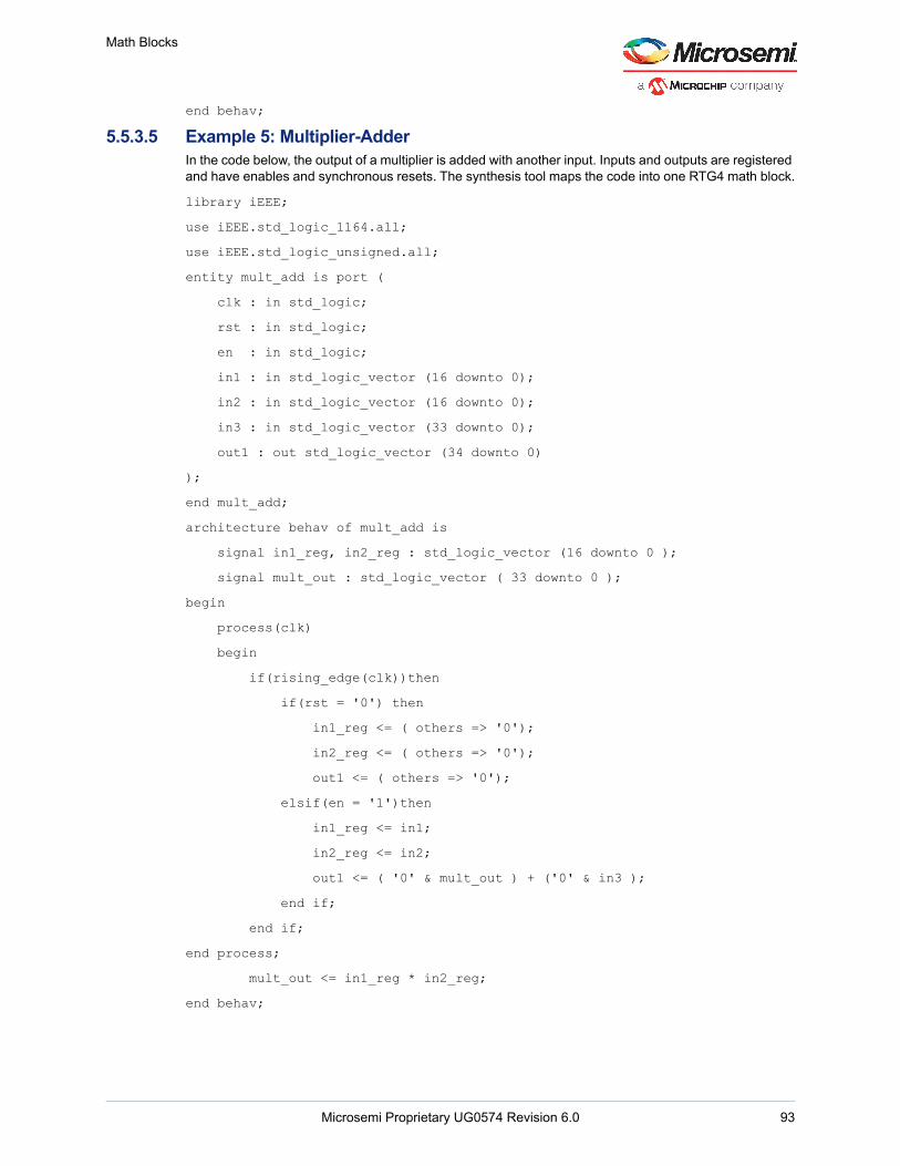
Math Blocks
end behav;5.5.3.5 Example 5: Multiplier-Adder
In the code below, the output of a multiplier is added with another input. Inputs and outputs are registered and have enables and synchronous resets. The synthesis tool maps the code into one RTG4 math block.
library iEEE;use iEEE.std_logic_1164.all;use iEEE.std_logic_unsigned.all;entity mult_add is port ( clk : in std_logic; rst : in std_logic; en : in std_logic; in1 : in std_logic_vector (16 downto 0); in2 : in std_logic_vector (16 downto 0); in3 : in std_logic_vector (33 downto 0); out1 : out std_logic_vector (34 downto 0));end mult_add;architecture behav of mult_add is signal in1_reg, in2_reg : std_logic_vector (16 downto 0 ); signal mult_out : std_logic_vector ( 33 downto 0 );begin process(clk) begin if(rising_edge(clk))then if(rst = '0') then in1_reg <= ( others => '0'); in2_reg <= ( others => '0'); out1 <= ( others => '0'); elsif(en = '1')then in1_reg <= in1; in2_reg <= in2; out1 <= ( '0' & mult_out ) + ('0' & in3 ); end if; end if;end process; mult_out <= in1_reg * in2_reg;end behav;
Microsemi Proprietary UG0574 Revision 6.0 93

Math Blocks
5.5.3.6 Example 6: Multiplier-SubtractorUser can implement multiplier and subtract logic in three methods. The synthesis tool places the logic differently, depending on how it is implemented.
• Subtract the result of multiplier from an input value (P = Cin – mult_out). The synthesis tool places all logics in the math block.
• Subtract a value from the result of the multiplier (P = mult_out – Cin). The synthesis tool places only the multiplier in the math block. The subtractor is implemented in the fabric logic outside the math block.• Unsigned MultSub Example (P = Cin – Mult_out) - Implemented in a single math block.• Unsigned MultSub Example (P = Cin – Mult_out) - Implemented in a single math block
library IEEE;use IEEE.std_logic_1164.all;use IEEE.std_logic_unsigned.all;entity mult_sub is port ( clk : in std_logic; rst : in std_logic; in1 : in std_logic_vector(16 downto 0); in2 : in std_logic_vector(16 downto 0); in3 : in std_logic_vector(33 downto 0); out1 : out std_logic_vector(33 downto 0));end mult_sub;architecture behav of mult_sub is signal in1_reg, in2_reg : std_logic_vector(16 downto 0); begin process(clk) begin if(rising_edge(clk))then if(rst = '0') then in1_reg <= ( others => '0'); in2_reg <= ( others => '0'); out1 <= ( others => '0'); else if(rising_edge(clk))then in1_reg <= in1; in2_reg <= in2; out1 <= in3 - (in1_reg * in2_reg); end if; end if; end if; end process;
Microsemi Proprietary UG0574 Revision 6.0 94

Math Blocks
end behav;– Unsigned MultSub Example (P = Mult - Cin) -
Multiplier is implemented in the math block and subtractor in the fabric logic
library IEEE;use IEEE.std_logic_1164.all;use IEEE.std_logic_unsigned.all;entity mult_sub is port ( clk : in std_logic; rst : in std_logic; in1 : in std_logic_vector(16 downto 0); in2 : in std_logic_vector(16 downto 0); in3 : in std_logic_vector(33 downto 0); out1 : out std_logic_vector(33 downto 0));end mult_sub;architecture behav of mult_sub is signal in1_reg, in2_reg : std_logic_vector(16 downto 0); begin process(clk) begin if(rising_edge(clk))then if(rst = '0') then in1_reg <= ( others => '0'); in2_reg <= ( others => '0'); out1 <= ( others => '0'); else if(rising_edge(clk))then in1_reg <= in1; in2_reg <= in2; out1 <= (in1_reg * in2_reg)-in3; end if; end if; end if; end process;end behav;
Microsemi Proprietary UG0574 Revision 6.0 95
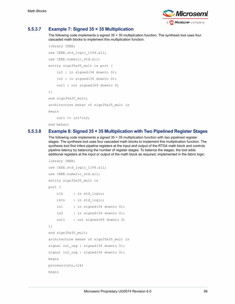
Math Blocks
5.5.3.7 Example 7: Signed 35 × 35 MultiplicationThe following code implements a signed 35 × 35 multiplication function. The synthesis tool uses four cascaded math blocks to implement this multiplication function.
library IEEE;use IEEE.std_logic_1164.all;use IEEE.numeric_std.all;entity sign35x35_mult is port ( in1 : in signed(34 downto 0); in2 : in signed(34 downto 0); out1 : out signed(69 downto 0));end sign35x35_mult;architecture behav of sign35x35_mult is begin out1 <= in1*in2;end behav;
5.5.3.8 Example 8: Signed 35 × 35 Multiplication with Two Pipelined Register StagesThe following code implements a signed 35 × 35 multiplication function with two pipelined register stages. The synthesis tool uses four cascaded math blocks to implement this multiplication function. The synthesis tool first infers pipeline registers at the input and output of the RTG4 math block and controls pipeline latency by balancing the number of register stages. To balance the stages, the tool adds additional registers at the input or output of the math block as required, implemented in the fabric logic.
library IEEE;use IEEE.std_logic_1164.all;use IEEE.numeric_std.all;entity sign35x35_mult is port ( clk : in std_logic; rstn : in std_logic; in1 : in signed(34 downto 0); in2 : in signed(34 downto 0); out1 : out signed(69 downto 0));end sign35x35_mult;architecture behav of sign35x35_mult is signal in1_reg : signed(34 downto 0);signal in2_reg : signed(34 downto 0); beginprocess(rstn,clk)begin
Microsemi Proprietary UG0574 Revision 6.0 96

Math Blocks
if(rstn ='0')then in1_reg <= (others => '0'); in2_reg <= (others => '0'); out1 <= (others => '0'); else if(rising_edge(clk))then in1_reg <= in1; in2_reg <= in2;out1 <= in1_reg*in2_reg; end if; end if;end process;end behav;
Microsemi Proprietary UG0574 Revision 6.0 97

Appendix: Supported Memory File Formats
6 Appendix: Supported Memory File Formats
Intel-Hex and Motorola-S file formats are supported. Implementation of these formats interprets data sets in bytes. If the memory width is 7 bits, every 8th bit in the data set is ignored. If the data width is 9 bits, two bytes are assigned to each memory address and the upper 7 bits of each 2-byte pair are ignored.
The following examples illustrate how the data is interpreted for various word sizes:
FF 11 EE 22 DD 33 CC 44 BB 55 (where, 55 is the MSB and FF is the LSB) for 32-bit word size:56
0x22EE11FF (address 0)0x44CC33DD (address 1)0x000055BB (address 2)For 16-bit word size:
0x11FF (address 0)0x22EE (address 1)0x33DD (address 2)0x44CC (address 3)0x55BB (address 4)For 8-bit word size:
0xFF (address 0)0x11 (address 1)0xEE (address 2)0x22 (address 3)0xDD (address 4)0x33 (address 5)0xCC (address 6)0x44 (address 7)0xBB (address 8)0x55 (address 9)For 9-bit word size:
0x11FF -> 0x01FF (address 0)0x22EE -> 0x00EE (address 1)0x33DD -> 0x01DD (address 2)0x44CC -> 0x00CC (address 3)0x55BB -> 0x01BB (address 4)
Note: For 9-bit, the upper 7-bits of the 2-bytes are ignored.
Microsemi Proprietary UG0574 Revision 6.0 98

Appendix: Supported Memory File Formats
INTEL-HEX
Intel Hex is an industry standard file format created by Intel. File extensions for these files are .hex and .ihx.
Memory contents are stored in ASCII files using hexadecimal characters. Each file contains a series of records (lines of text) delimited by new line, '\n', characters and each record starts with a ':' character. For more information about this format, see the Intel-Hex Record Format Specification.
The Intel Hex record is composed of five fields and is arranged as:
:llaaaatt[dd...]ccWhere:
• : - Start code of every Intel Hex record• ll - Byte count of the data field• aaaa - 16-bit address of the beginning of the memory position for the data. Address is big endian.• tt - Record type, defines the data field:• 00 - Data record• 01 - End of file record• 02 - Extended segment address record• 03 - Start segment address record (ignored by Microsemi SoC tools)• 04 - Extended linear address record• 05 - Start linear address record (ignored by Microsemi SoC tools)• [dd...] - Sequence of n bytes of the data. n is equivalent to what was specified in the ll field• cc - Checksum of count, address, and dataExample Intel Hex record:
:0300300002337A1EMOTOROLA S-Record
Motorola S-Record is an industry standard file format created by Motorola. The file extension for these files is .s.
This format uses ASCII files, hex characters, and records to specify memory content similar to the Intel-Hex format. See the Motorola S-record description document for more information about this format. The RAM Content Manager uses only the S1 through S3 record types. The other record types are ignored.
The major difference between Intel-Hex and Motorola S is the record formats and extra error checking features that are incorporated into the Motorola S-record.
In both formats, memory content is specified by providing a starting address and a data set. The upper bits of the data set are loaded into the starting address and leftovers overflow into the adjacent addresses until the entire data set has been used.
The Motorola S-record is composed of six fields and arranged as follows:
Stllaaaa[dd...]ccWhere:
• S - Start code of every Motorola S-record• t - Record type, defines the data field• ll - Byte count of the data field• aaaa - 16-bit address of the beginning of the memory position for the data. Address is big endian.• [dd...] - Sequence of n bytes of the data; n is equivalent to what was specified in the ll field• cc - Checksum of count, address, and data Example Motorola S-record:
S10a0000112233445566778899FFFA
Microsemi Proprietary UG0574 Revision 6.0 99

Appendix: Supported Memory File Formats
MEMFILE (RAM Content Manager output file)
Transfer of RAM data (from the RAM Content Manager) to test equipment is accomplished via MEM files.
The contents of RAM is first organized into the logical layer and then reorganized to fit the hardware layer. Then it is stored in MEM files that are read by other systems and used for testing. The MEM files are named according to the logical structure of RAM elements created by the configurator. In this scheme, the highest order RAM blocks are named CORE_R0C0.mem, where R stands for row and C stands for column. For multiple RAM blocks, the naming continues with CORE_R0C1, CORE_R0C2, CORE_R1C0, and so on.
The data intended for the RAM is stored as ASCII 1s and 0s within the file. Each memory address occupies one line. Words from logical layer blocks are concatenated or split in order to make them fit efficiently within the hardware blocks. If the logical layer width is less than the hardware layer, two or more logical layer words are concatenated to form one hardware layer word. In this case, the lowest bits of the hardware word are made up of the lower address data bits from the logical layer. If the logical layer width is more than the hardware layer, the words are split, placing the lower bits in lower addresses.
If the logical layer words do not fit cleanly into the hardware layer words, the most significant bit of the hardware layer words is not used and defaulted to zero. This is also done when the logical layer width is 1 in order to avoid having leftover memory at the end of the hardware block.
Microsemi Proprietary UG0574 Revision 6.0 100

Appendix: Macro
7 Appendix: Macro
7.1 LSRAM MacroThe LSRAM macro (RAM1K18_RT) in the Libero SoC IP macro library can be used directly to instantiate the LSRAM block in the design. The LSRAM block must be configured with appropriate values of the static signals. The following figure shows the LSRAM macro (RAM1K18_RT).
Figure 92 • LSRAM Configurator
Note: Static inputs are defined at design time and need to be tied to 0 or 1.
7.1.1 A_WIDTH and B_WIDTHThe following table lists the width/depth mode selections for each port. Two-port mode is in effect when the width of at least one port is 36, and A_WIDTH indicates the read width while B_WIDTH indicates the write width.
Table 28 • Depth × Width Mode Selection
Depth x Width A_WIDTH/B_WIDTH2Kx9, 2Kx12 00
1Kx18 01
512x36 (Two-port) 10
Microsemi Proprietary UG0574 Revision 6.0 101

Appendix: Macro
7.1.2 A_WEN and B_WENThe following table lists the write/read control signals for each port. Two-port mode is in effect when the width of at least one port is 36, and read operation is always enabled.
7.1.3 A_ADDR and B_ADDRThe following table lists the address buses for the two ports. 11 bits are needed to address the 2K independent locations in x9 mode. In wider modes, fewer address bits are used. The required bits are MSB justified and unused LSB bits must be tied to 0. A_ADDR is synchronized to A_CLK while B_ADDR is synchronized to B_CLK. A_ADDR provides the read-address while B_ADDR provides the write address.
7.1.4 A_DIN and B_DINThe following table lists the data input buses for the two ports. The required bits are LSB justified and unused MSB bits must be tied to 0. For two-port mode when the write data width is more than 18-bits, A_DIN provides the MSB of the write data while B_DIN provides the LSB of the write-data.
Table 29 • Write/Read Operation Select
Depth x Width A_WEN/B_WEN1
1. A_WEN/B_WEN = 1 if ECC mode is used.
Result2Kx9, 2Kx12 00 Perform a read operation
2Kx9, 2Kx12 11 Perform a write operation
1Kx18 01 Write [8:0]
10 Write [17:9]
11 Write [17:0]
512x36 (Two-port) B_WEN[0] = 1 Write B_DIN[8:0]
B_WEN[1] = 1 Write B_DIN[17:9]
A_WEN[0] = 1 Write A_DIN[8:0]
A_WEN[1] = 1 Write A_DIN[17:9]
Table 30 • Address Bus Used and Unused Bits
Depth x Width
A_ADDR/B_ADDR
Used BitsUnused Bits(must be tied to 0)
2Kx9, 2Kx12 [10:0] None
1Kx18 [10:1] [0]
512x36 (Two-port) [10:2] [1:0]
Table 31 • Data Input Buses Used and Unused Bits
Depth x Width
A_DIN/B_DIN
Used BitsUnused Bits(must be tied to 0)
2Kx9 [8:0] [17:9]
2Kx12 [11:0] [17:12]
1Kx18 [17:0] None
Microsemi Proprietary UG0574 Revision 6.0 102

Appendix: Macro
7.1.5 A_DOUT and B_DOUTThe following table lists the data output buses for the two ports. The required bits are LSB justified. A_DOUT provides the MSB of the read-data while B_DOUT provides the LSB of the read-data.
7.1.6 A_BLK and B_BLKThe following table lists the block-port select control signals for the two ports. A_BLK is synchronized by A_CLK while B_BLK is synchronized to B_CLK. Two-port mode is in effect when the width of at least one port is 36, and A_BLK controls the read operation while B_BLK controls the write operation.
7.1.7 A_WMODE and B_WMODEIn true dual-port write mode:
• Logic 00 = Read-data port holds the previous value.• All other values are reserved and must not be used.
7.1.8 A_CLK and B_CLKAll signals in ports A and B are synchronous to the corresponding port clock. All address, data, block-port select, write-enable and read-enable inputs must be set up before the rising edge of the clock. The read
512x36 (Two-port) A_DIN[17:0] is [35:18] B_DIN[17:0] is [17:0]
None
Table 32 • Data Output Buses Used and Unused Bits
Depth x WidthA_DOUT/B_DOUT
Used Bits Unused Bits2Kx9 [8:0] [17:9]
2Kx12 [11:0] [17:12]
1Kx18 [17:0] None
512x36 (Two-port) A_DOUT[17:0] is [35:18]B_DOUT[17:0] is [17:0]
None
Table 33 • Block-Port Select
Block-portSelect Signal Value ResultA_BLK[2:0] 111 Perform read or write operation on Port A. In 36 width mode, perform a read
operation from both ports A and B.
A_BLK[2:0] Any one bit is 0 No operation in memory from Port A. Port A read-data will be forced to 0. In 36 width mode, the read-data from both ports A and B will be forced to 0.
B_BLK[2:0] 111 Perform read or write operation on Port B. In 36 width mode, perform a write operation to both ports A and B.
B_BLK[2:0] Any one bit is 0 No operation in memory from Port B. Port B read-data will be forced to 0, unless it is a 36 width mode and write operation to both ports A and B is gated.
Table 31 • Data Input Buses Used and Unused Bits (continued)
Depth x Width
A_DIN/B_DIN
Used BitsUnused Bits(must be tied to 0)
Microsemi Proprietary UG0574 Revision 6.0 103

Appendix: Macro
or write operation begins with the rising edge. Two-port mode is in effect when the width of at least one port is 36, and A_CLK provides the read clock while B_CLK provides the write clock.
Microsemi Proprietary UG0574 Revision 6.0 104

Appendix: Macro
7.1.9 A_REN and B_RENEnables read operation from the memory on the corresponding port.
Read-data Pipeline Register Control signals
A_DOUT_BYPASS and B_DOUT_BYPASS
A_DOUT_EN and B_DOUT_EN
A_DOUT_SRST_N and B_DOUT_SRST_N
Two-port mode is in effect when the width of at least one port is 36, and the A_DOUT register signals control the MSB of the read-data while the B_DOUT register signals control the LSB of the read-data.
7.1.10 ARST_NConnects the Read-data pipeline registers to the global Asynchronous-reset signal.
7.1.11 ECC and ECC_DOUT_BYPASSControls ECC operation.
• ECC = 0: Disable ECC.• ECC = 1, ECC_DOUT_BYPASS = 0: Enable ECC Pipelined.
• During writes, ECC Pipelined mode inserts an additional clock cycle to encode the write data before it is actually written into the memory array.
• During reads, ECC Pipelined mode inserts an additional clock cycle to decode the data read from memory before it is presented on DOUT.
• ECC = 1, ECC_DOUT_BYPASS = 1: Enable ECC Non-pipelined.
7.1.12 A_SB_CORRECT and B_SB_CORRECTOutput flag indicates single-bit correction was performed on the corresponding port.
7.1.13 A_DB_DETECT and B_DB_DETECTOutput flag indicates double-bit detection was performed on the corresponding port.
7.1.13.1 DELENEnable Single-event Transient mitigation.
7.1.13.2 SECURITYControl signal, when 1 locks the entire RAM1K18_RT memory from being accessed by the SII.
7.1.13.3 BUSYThis output indicates that the RAM1K18_RT memory is being accessed by the SII.
7.2 µSRAM MacroThe µSRAM macro (RAM64×12) in Libero SoC can be used directly to instantiate µSRAM in the design. µSRAM must be configured correctly with appropriate values provided to the static signals before instantiating in the design. Instantiating µSRAM primitives in a design is not recommended. See Inserting an µSRAM Memory Macro for the recommended methods of instantiating memory into a user design. The following figure shows the µSRAM macro (RAM64×12 available in the Libero SoC macro library.
Microsemi Proprietary UG0574 Revision 6.0 105

Appendix: Macro
Figure 93 • µSRAM Configurator
7.2.1 A_WIDTH, B_WIDTH, and C_WIDTHThe following table lists the width/depth mode selections for each port.
7.2.2 C_WENThis is the write-enable signal for port C.
Table 34 • Width/Depth Mode Selection
Depth x Width A_WIDTH/B_WIDTH/C_WIDTH128x9, 128x12 0
64x16, 64x18 1
Microsemi Proprietary UG0574 Revision 6.0 106

Appendix: Macro
7.2.3 A_ADDR, B_ADDR, and C_ADDRThe following table lists the address buses for each port. 7 bits are required to address 128 independent locations in x9 mode. In wider modes, fewer address bits are used. The required bits are MSB justified and unused LSB bits must be tied to 0.
7.2.4 C_DINThe following table lists the write-data input for port C. The required bits are LSB justified and unused MSB bits must be tied to 0.
7.2.5 A_DOUT and B_DOUTThe following table lists the read-data output buses for ports A and B. The required bits are LSB justified.
Table 35 • Address Buses Used and Unused Bits
Depth x Width
A_ADDR/B_ADDR/C_ADDR
Used BitsUnused Bits(must be tied to 0)
128x9 [6:0] None
64x18 [6:1] [0]
Table 36 • Data Input Bus Used and Unused Bits
Depth x Width
C_DIN
Used BitsUnused Bits(must be tied to 0)
128x9 [8:0] [17:9]
128x12 [11:0] [17:12]
64x18 [17:0] None
Table 37 • Data Output Used and Unused Bits
Depth x WidthA_DOUT/B_DOUT
Used Bits Unused Bits128x9 [8:0] [17:9]
128x12 [11:0] [17:12]
64x18 [17:0] None
Microsemi Proprietary UG0574 Revision 6.0 107
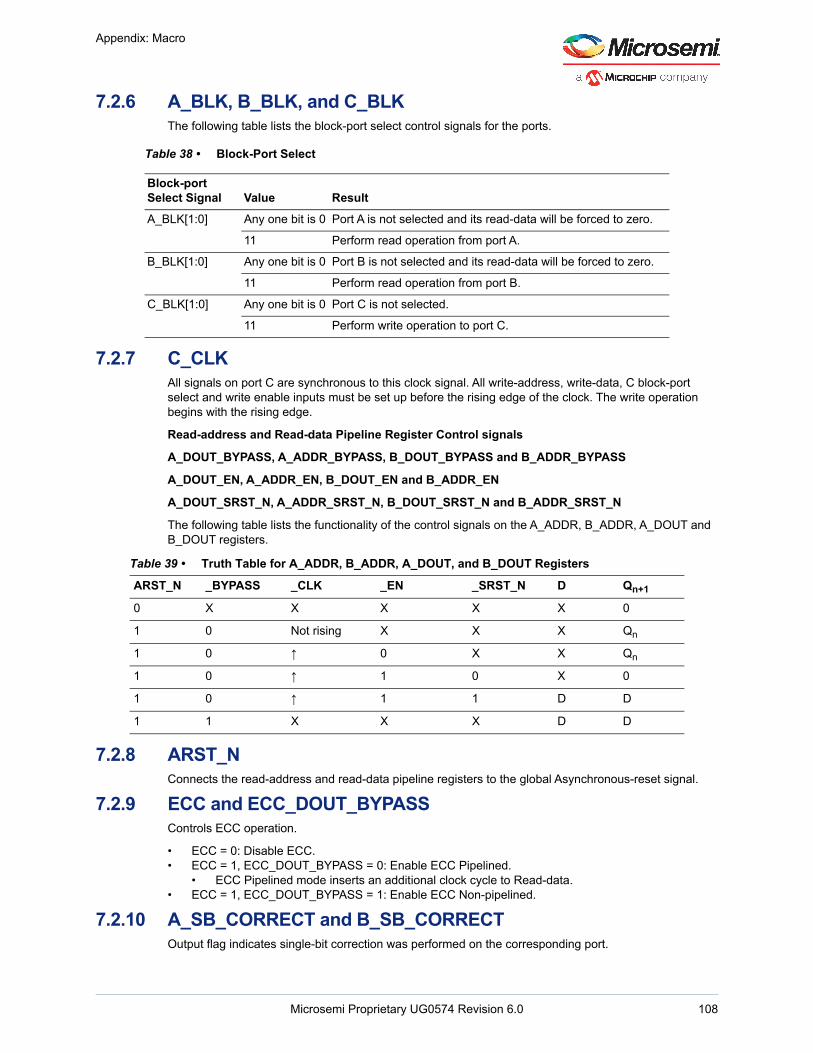
Appendix: Macro
7.2.6 A_BLK, B_BLK, and C_BLKThe following table lists the block-port select control signals for the ports.
7.2.7 C_CLKAll signals on port C are synchronous to this clock signal. All write-address, write-data, C block-port select and write enable inputs must be set up before the rising edge of the clock. The write operation begins with the rising edge.
Read-address and Read-data Pipeline Register Control signals
A_DOUT_BYPASS, A_ADDR_BYPASS, B_DOUT_BYPASS and B_ADDR_BYPASS
A_DOUT_EN, A_ADDR_EN, B_DOUT_EN and B_ADDR_EN
A_DOUT_SRST_N, A_ADDR_SRST_N, B_DOUT_SRST_N and B_ADDR_SRST_N
The following table lists the functionality of the control signals on the A_ADDR, B_ADDR, A_DOUT and B_DOUT registers.
7.2.8 ARST_NConnects the read-address and read-data pipeline registers to the global Asynchronous-reset signal.
7.2.9 ECC and ECC_DOUT_BYPASSControls ECC operation.
• ECC = 0: Disable ECC.• ECC = 1, ECC_DOUT_BYPASS = 0: Enable ECC Pipelined.
• ECC Pipelined mode inserts an additional clock cycle to Read-data.• ECC = 1, ECC_DOUT_BYPASS = 1: Enable ECC Non-pipelined.
7.2.10 A_SB_CORRECT and B_SB_CORRECTOutput flag indicates single-bit correction was performed on the corresponding port.
Table 38 • Block-Port Select
Block-portSelect Signal Value ResultA_BLK[1:0] Any one bit is 0 Port A is not selected and its read-data will be forced to zero.
11 Perform read operation from port A.
B_BLK[1:0] Any one bit is 0 Port B is not selected and its read-data will be forced to zero.
11 Perform read operation from port B.
C_BLK[1:0] Any one bit is 0 Port C is not selected.
11 Perform write operation to port C.
Table 39 • Truth Table for A_ADDR, B_ADDR, A_DOUT, and B_DOUT Registers
ARST_N _BYPASS _CLK _EN _SRST_N D Qn+1
0 X X X X X 0
1 0 Not rising X X X Qn
1 0 ↑ 0 X X Qn
1 0 ↑ 1 0 X 0
1 0 ↑ 1 1 D D
1 1 X X X D D
Microsemi Proprietary UG0574 Revision 6.0 108

Appendix: Macro
7.2.11 A_DB_DETECT and B_DB_DETECTOutput flag indicates double-bit detection was performed on the corresponding port.
7.2.11.1 DELENEnable Single-event Transient mitigation.
7.2.11.2 SECURITYControl signal, when 1 locks the entire RAM64x18_RT memory from being accessed by the SII.
7.2.11.3 BUSYThis output indicates that the RAM64x18_RT memory is being accessed by the SII.
7.3 Math Block Macro18 bit x 18 bit multiply-accumulate MACC block. The math block can accumulate the current multiplication product with a previous result, a constant, a dynamic value, or a result from another math block. Each math block can also be configured to perform a Dot-product operation. All the signals of the math block (except CDIN and CDOUT) have optional registers.
Figure 94 • Math Block Configurator
Microsemi Proprietary UG0574 Revision 6.0 109

Appendix: Macro
Table 40 • Ports List of Math Block Configurator
Pin Name Pin Direction Type Polarity DescriptionDOTP Input Static Active high Dot-product mode.
When DOTP = 1, MACC block performs Dotproduct of two pairs of 9-bit operands.When DOTP = 0, it is called the normal mode.
SIMD Input Static Reserved. Must be 0.
CLK[1:0] Input Dynamic Rising edge Input clocks.CLK[1] is the clock for A[17:9], B[17:9], C[43:18], P[43:18], OVFL_CARRYOUT, ARSHFT17, CDSEL, FDBKSEL and SUB registers.CLK[0] is the clock for A[8:0], B[8:0], C[17:0], CARRYIN and P[17:0].In normal mode, ensure CLK[1] = CLK[0].
A[17:0] Input Dynamic Active high Input data A.
A_BYPASS[1:0] Input Static Active high Bypass data A registers.A_BYPASS[1] is for A[17:9]. Connect to 1, if not registered.A_BYPASS[0] is for A[8:0]. Connect to 1, if not registered.In normal mode, ensure A_BYPASS[0] = A_BYPASS[1].
A_ARST_N[1:0] Input Dynamic Active low Asynchronous reset for data A registers.Connect both A_ARST_N[1] and =A_ARST_N[0] to 1 or to the global Asynchronous reset of the design
A_SRST_N[1:0] Input Dynamic Active low Synchronous reset for data A registers.A_SRST_N[1] is for A[17:9]. Connect to 1, if not registered.A_SRST_N[0] is for A[8:0]. Connect to 1, if not registered.In normal mode, ensure A_SRST_N[1] = A_SRST_N[0].
A_EN[1:0] Input Dynamic Active high Enable for data A registers.A_EN[1] is for A[17:9]. Connect to 1, if not registered.A_EN[0] is for A[8:0]. Connect to 1, if not registered.In normal mode, ensure A_EN[1] = A_EN[0].
B[17:0] Input Dynamic Active high Input data B.
B_BYPASS[1:0] Input Static Active high Bypass data B registers.B_BYPASS[1] is for B[17:9]. Connect to 1, if not registered.B_BYPASS[0] is for B[8:0]. Connect to 1, if not registered.In normal mode, ensure B_BYPASS[0] = B_BYPASS[1].
B_ARST_N[1:0] Input Dynamic Active low Asynchronous reset for data B registers.In normal mode, ensure to connect both B_ARST_N[1] and B_ARST_N[0] to 1 or to the global Asynchronous reset of the design.
Microsemi Proprietary UG0574 Revision 6.0 110

Appendix: Macro
B_SRST_N[1:0] Input Dynamic Active low Synchronous reset for data B registers.B_SRST_N[1] is for B[17:9]. Connect to 1, if not registered.B_SRST_N[0] is for B[8:0]. Connect to 1, if not registered.In normal mode, ensure B_SRST_N[1] = B_SRST_N[0].
B_EN[1:0] Input Dynamic Active high Enable for data B registers.B_EN[1] is for B[17:9]. Connect to 1, if not registered.B_EN[0] is for B[8:0]. Connect to 1, if not registered.In normal mode, ensure B_EN[1] = B_EN[0].
P[43:0] Output Active high Result data.Normal modeP = D + (CARRYIN + C) + (A * B), when SUB = 0P = D + (CARRYIN + C) - (A * B), when SUB = 1Dot-product modeP = D + (CARRYIN + C) + 512 * ((AL * BH) + (AH * BL)), when SUB = 0P = D + (CARRYIN + C) - 512 * ((AL * BH) + (AH * BL)), when SUB = 1Notation:AL = A[8:0], AH = A[17:9]BL = B[8:0], BH = B[17:9]See Table 43, page 115 to see how operand D is obtained from P, CDIN or 0.
OVFL_CARRYOUT Output Active high Overflow or CarryOutOverflow when OVFL_CARRYOUT_SEL = 0 OVFL_CARRYOUT = (SUM[45] ^ SUM[44]) | (SUM[44] ^ SUM[43])CarryOut when OVFL_CARRYOUT_SEL =1OVFL_CARRYOUT = C[43] ^ D[43] ^ SUM[44]
P_BYPASS[1:0] Input Static Active high Bypass result P registers.P_BYPASS[1] is for P[43:18] and OVFL_CARRYOUT. Connect to 1, if not registered.P_BYPASS[0] is for P[17:0]. Connect to 1, if not registered.In normal mode, ensure P_BYPASS[0] = P_BYPASS[1].
P_ARST_N[1:0] Input Dynamic Active low Asynchronous reset for result P registers.Connect both P_ARST_N[1] and P_ARST_N[0] to 1 or to the global Asynchronous reset of the design
Table 40 • Ports List of Math Block Configurator (continued)
Pin Name Pin Direction Type Polarity Description
Microsemi Proprietary UG0574 Revision 6.0 111

Appendix: Macro
P_SRST_N[1:0] Input Dynamic Active low Synchronous reset for result P registers.P_SRST_N[1] is for P[43:18] and OVFL_CARRYOUT. Connect to 1, if not registered.P_SRST_N[0] is for P[17:0]. Connect to 1, if not registered.In normal mode, ensure P_SRST_N[1] = P_SRST_N[0].
P_EN[1:0] Input Dynamic Active high Enable for result P registers.P_EN[1] is for P[43:18] and OVFL_CARRYOUT. Connect to 1, if not registered.P_EN[0] is for P[17:0]. Connect to 1, if not registered.In normal mode, ensure P_EN[1] = P_EN[0].
CDOUT[43:0] Output Cascade Active high Cascade output of result P.CDOUT is the same as P. The entire bus must either be dangling or drive an entire CDIN of another MACC block in cascaded mode.
CARRYIN Input Dynamic Active high CarryIn for operand C.
C[43:0] Input Dynamic Active high Routed input for operand C.In Dot-product mode, connect C[8:0] to the CARRYIN.
C_BYPASS[1:0] Input Static Active high Bypass data C registers.C_BYPASS[1] is for C[43:18]. Connect to 1, if not registered.C_BYPASS[0] is for C[17:0] and CARRYIN.Connect to 1, if not registered.In normal mode, ensure C_BYPASS[0] = C_BYPASS[1].
C_ARST_N[1:0] Input Dynamic Active low Asynchronous reset for data C registers.Connect both C_ARST_N[1] andC_ARST_N[0] to 1 or to the global Asynchronous reset of the design.
C_SRST_N[1:0] Input Dynamic Active low Synchronous reset for data C registers.C_SRST_N[1] is for C[43:18]. Connect to 1, if not registered.C_SRST_N[0] is for C[17:0] and CARRYIN.Connect to 1, if not registered.In normal mode, ensure C_SRST_N[1] = C_SRST_N[0].
C_EN[1:0] Input Dynamic Active high Enable for data C registers.C_EN[1] is for C[43:18]. Connect to 1, if not registered.C_EN[0] is for C[17:0] and CARRYIN.Connect to 1, if not registered.In normal mode, ensure C_EN[1] = C_EN[0].
Table 40 • Ports List of Math Block Configurator (continued)
Pin Name Pin Direction Type Polarity Description
Microsemi Proprietary UG0574 Revision 6.0 112

Appendix: Macro
CDIN[43:0] Input Cascade Active high Cascaded input for operand D.The entire bus must be driven by an entire CDOUT of another MACC block. In Dotproduct mode the CDOUT must also be generated by a MACC block in Dot-product mode.See Table 43, page 115 to see how CDIN is propagated to operand D.
ARSHFT17 Input Dynamic Active high Arithmetic right-shift for operand D.When asserted, a 17-bit arithmetic right-shift is performed on operand D going into the accumulator. See Table 43, page 115 to see how operand D is obtained from P, CDIN or 0.
ARSHFT17_BYPASS Input Static Active high Bypass ARSHFT17 register. Connect to 1, if not registered.
ARSHFT17_AL_N Input Dynamic Active low Asynchronous load for ARSHFT17 register.Connect to 1 or to the global Asynchronous reset of the design.When asserted, ARSHFT17 register is loaded with ARSHFT17_AD.
ARSHFT17_AD Input Static Active high Asynchronous load data for ARSHFT17 register.
ARSHFT17_SL_N Input Dynamic Active low Synchronous load for ARSHFT17 register.Connect to 1, if not registered. See Table 41, page 115.
ARSHFT17_SD_N Input Static Active low Synchronous load data for ARSHFT17 register. See Table 41, page 115.
ARSHFT17_EN Input Dynamic Active high Enable for ARSHFT17 register. Connect to 1, if not registered. See Table 41, page 115.
CDSEL Input Dynamic Active high Select CDIN for operand D.When CDSEL = 1, propagate CDIN.When CDSEL = 0, propagate 0 or P depending on FDBKSEL.See Table 41, page 115 to see how operand D is obtained from P, CDIN or 0.
CDSEL_BYPASS Input Static Active high Bypass CDSEL register. Connect to 1, if not registered.
CDSEL_AL_N Input Dynamic Active low Asynchronous load for CDSEL register.Connect to 1 or to the global Asynchronous reset of the design.When asserted, CDSEL register is loaded with CDSEL_AD.
CDSEL_AD Input Static Active high Asynchronous load data for CDSEL register.
CDSEL_SL_N Input Dynamic Active low Synchronous load for CDSEL register.Connect to 1, if not registered. See Table 41, page 115.
CDSEL_SD_N Input Static Active low Synchronous load data for CDSEL register.See Table 41, page 115.
CDSEL_EN Input Dynamic Active high Enable for CDSEL register. Connect to 1, if not registered. See Table 41, page 115.
Table 40 • Ports List of Math Block Configurator (continued)
Pin Name Pin Direction Type Polarity Description
Microsemi Proprietary UG0574 Revision 6.0 113

Appendix: Macro
FDBKSEL Input Dynamic Active high Select the feedback from P for operand D.When FDBKSEL = 1, propagate the current value of result P register. Ensure P_BYPASS[1] = 0 and CDSEL = 0.When FDBKSEL = 0, propagate 0. Ensure CDSEL = 0.See Table 43, page 115 to see how operand D is obtained from P, CDIN or 0.
FDBKSEL_BYPASS Input Static Active high Bypass FDBKSEL register. Connect to 1, if not registered.
FDBKSEL_AL_N Input Dynamic Active low Asynchronous load for FDBKSEL register.Connect to 1 or to the global Asynchronous reset of the design.When asserted, FDBKSEL register is loaded with FDBKSEL_AD.
FDBKSEL_AD Input Static Active high Asynchronous load data for FDBKSEL register.
FDBKSEL_SL_N Input Dynamic Active low Synchronous load for FDBKSEL register.Connect to 1, if not registered. See Table 41, page 115.
FDBKSEL_SD_N Input Static Active low Synchronous load data for FDBKSEL register.See Table 41, page 115.
FDBKSEL_EN Input Dynamic Active high Enable for FDBKSEL register. Connect to 1, if not registered. See Table 41, page 115.
SUB Input Dynamic Active high Subtract operation.
SUB_BYPASS Input Static Active high Bypass SUB register. Connect to 1, if not registered.
SUB_AL_N Input Dynamic Active low Asynchronous load for SUB register.Connect to 1 or to the global Asynchronous reset of the design.When asserted, SUB register is loaded with SUB_AD.
SUB_AD Input Static Active high Asynchronous load data for SUB register.
SUB_SL_N Input Dynamic Active low Synchronous load for SUB register. Connect to 1, if not registered. See Table 41, page 115.
SUB_SD_N Input Static Active low Synchronous load data for SUB register. See Table 41, page 115.
SUB_EN Input Dynamic Active high Enable for SUB register. Connect to 1, if not registered. See Table 41, page 115.
Table 40 • Ports List of Math Block Configurator (continued)
Pin Name Pin Direction Type Polarity Description
Microsemi Proprietary UG0574 Revision 6.0 114

Appendix: Macro
Table 41 • Truth Table for Control Registers ARSHFT17, CDSEL, FDBKSEL, and SUB
_AL_N _AD _BYPASS _CLK _EN _SL_N _SD_N D Qn+1
0 AD X X X X X X AD
1 X 0 Not rising X X X X Qn
1 X 0 ↑ 0 X X X Qn
1 X 0 ↑ 1 0 SDn X !SDn
1 X 0 ↑ 1 1 X D D
1 X 1 X 0 X X X Qn
1 X 1 X 1 0 SDn X !SDn
1 X 1 X 1 1 X D D
Table 42 • Truth Table - Data Registers A, B, C, CARRYIN, P, and OVFL_CARRYOUT
_ARST_N _BYPASS _CLK _EN _SRST_N D Qn+1
0 X X X X X 0
1 0 Not rising X X X Qn
1 0 ↑ 0 X X Qn
1 0 ↑ 1 0 X 0
1 0 ↑ 1 1 D D
1 1 X 0 X X Qn
1 1 X 1 0 X 0
1 1 X 1 1 D D
Table 43 • Truth Table - Propagating Data to Operand D
FDBKSEL CDSEL ARSHFT17 Operand D
0 0 X 44'b0
X 1 0 CDIN[43:0]
X 1 1 {{17{CDIN[43]}},CDIN[43:17]}
1 0 0 P[43:0]
1 0 1 {{17{P[43]}},P[43:17]}
Microsemi Proprietary UG0574 Revision 6.0 115
Glossary
8 Glossary
8.1 AcronymsCCCClock conditioning circuits
DDRIODouble data rate input output
ECCError correction code
ESDElectrostatic discharge protection
FDDRController for external DDR memory
HSTLHigh-speed transceiver logic
IOAInput output analog
IODInput output digital
LPDDRLow power double data rate memory
LPELow power exit
LSBLeast significant bit
LSRAMLarge static random access memory
LVDSBus LVDS
LVPECLLow-voltage positive emitter coupled logic
LVTTLLow voltage transistor transistor logic
MLVDSMultipoint LVDS
MSBMost significant bit
MSIOMulti-standard I/O
Microsemi Proprietary UG0574 Revision 6.0 116

Glossary
MVNMultiView Navigator
ODTOn-die termination
RSDSReduced swing differential signaling
SerDesSerializer/deserializer
SSTLStub series terminated logic
STMRSelf-corrected triple module redundancy
µSRAMMicro static random access memory
Microsemi Proprietary UG0574 Revision 6.0 117
Glossary
8.2 TerminologyBus KeeperHolds the signal on an I/O pin at its last driven state.
ClustersClusters are formed by grouping a certain number of logic elements and interconnecting them. This is related to the clustered routing architecture of the RTG4 FPGA fabric.
Dual-Port ModeSRAM with two independent ports through which both read and write operation can be done.
Flow-Through ReadA read operation performed with the output not being registered by the output pipeline registers.
Hot InsertionCapability to connect I/O to external circuitry even after power-up.
I/O ClusterI/O cluster is formed by grouping either three or four I/O modules.
I/O ModuleThe logic element consists of flip-flops and routing multiplexers. This logic element interfaces the user I/Os to fabric routing.
InferenceUsing RTL to infer mathblocks
Inter-Cluster RoutingInter-cluster routing refers to routing resources between various types of clusters.
Interface ClusterAn interface cluster is formed by grouping 12 interface logic elements.
Interface LogicThe logic element consists of a 4-input LUT and a STMR-flip-flop. This logic element interfaces the hard macros (LSRAMs, uSRAMs, and mathblocks) to fabric routing.
Intra-Cluster RoutingIntra-cluster routing refers to routing resources existing inside a specific cluster.
Logic ClusterA logic cluster is formed by grouping 12 logic elements.
Logic ElementThe basic logic element in the RTG4 FPGA fabric, consisting of a 4-input LUT, a D-flip-flop, and a dedicated carry chain.
Low Power ExitLogic for the chip to come out from low power state.
Multi-ChannelingMulti-threading done for a chain of mathblocks
Multi-ThreadingUsing a math block for performing more than one computation by time multiplexing it.
Pipelined OperationThe mode of operation where the mathblock output is registered at the pipeline registers.
Pipelined ReadA read operation performed with the output being registered by the output pipeline registers.
Microsemi Proprietary UG0574 Revision 6.0 118

Glossary
Simple WriteA write operation in which the data written does not appear on the SRAM output ports.
STMRSelf-corrected triple module redundancy
Transparent ModeNon-registered/Non-pipelined mode
Two-Port ModeSRAM with two ports, one dedicated to read operations and the other dedicated to write operations.
Microsemi Proprietary UG0574 Revision 6.0 119