
UCD3138 Highly Integrated Digital Controller for Isolated ...
92
Product Folder Order Now Technical Documents Tools & Software Support & Community An IMPORTANT NOTICE at the end of this data sheet addresses availability, warranty, changes, use in safety-critical applications, intellectual property matters and other important disclaimers. PRODUCTION DATA. UCD3138 SLUSAP2I – MARCH 2012 – REVISED JANUARY 2017 UCD3138 Highly Integrated Digital Controller for Isolated Power 1 Device Overview 1 1.1 Features 1 • Digital Control of up to 3 Independent Feedback Loops – Dedicated PID-Based hardware – 2-Pole/2-Zero Configurable – Nonlinear Control • Up to 16 MHz Error Analog-to-Digital Converter (EADC) – Configurable Resolution as Small as 1mV/LSB – Automatic Resolution Selection – Up to 8x Oversampling – Hardware-Based Averaging (up to 8x) – 14-Bit Effective Digital-to-Analog Converter (DAC) – Adaptive Sample Trigger Positioning • Up to 8 High Resolution Digital Pulse Width Modulated (DPWM) Outputs – 250-ps Pulse Width Resolution – 4-ns Frequency Resolution – 4-ns Phase Resolution – Adjustable Phase Shift Between Outputs – Adjustable Dead-band Between Pairs – Cycle-by-Cycle Duty Cycle Matching – Up to 2-MHz Switching Frequency • Configurable PWM Edge Movement – Trailing Modulation – Leading Modulation – Triangular Modulation • Configurable Feedback Control – Voltage Mode – Average Current Mode – Peak Current Mode Control – Constant Current – Constant Power • Configurable Modulation Methods – Frequency Modulation – Phase Shift Modulation – Pulse Width Modulation • Fast, Automatic, and Smooth Mode Switching – Frequency Modulation and PWM – Phase Shift Modulation and PWM • High Efficiency and Light Load Management – Burst Mode – Ideal Diode Emulation – Synchronous Rectifier Soft On/Off – Low IC Standby Power • Soft Start / Stop with and without Prebias • Fast Input Voltage Feed Forward Hardware • Primary Side Voltage Sensing • Copper Trace Current Sensing • Flux and Phase Current Balancing for Nonpeak Current Mode Control Applications • Current Share Bus Support – Analog Average – Master and Slave • Feature Rich Fault Protection Options – 7 High-Speed Analog Comparators – Cycle-by-Cycle Current Limiting – Programmable Fault Counting – External Fault Inputs – 10 Digital Comparators – Programmable Blanking Time • Synchronization of DPWM Waveforms Between Multiple UCD3138 devices • 14-Channel, 12-Bit, 267-ksps General-Purpose ADC with Integrated – Programmable Averaging Filters – Dual Sample and Hold • Internal Temperature Sensor • Fully Programmable High-Performance 31.25 MHz, 32-Bit ARM7TDMI-S™ Processor – 32KB of Program Flash – 2KB of Data Flash with ECC – 4KB of Data RAM – 4KB of Boot ROM Enables Firmware Boot-Load in the Field via I 2 C or UART • Communication Peripherals –I 2 C/PMBus – 2 UARTs on UCD3138RGC (64-Pin QFN) – 1 UART on UCD3138RHA/UCD3138RMH (40-Pin QFN) and UCD3138RJA (40-Pin VQFN) • Timer Capture with Selectable Input Pins • Up to 5 Additional General Purpose Timers • Built In Watchdog: BOD and POR • 64-Pin QFN and 40-Pin QFN Packages • Operating Temperature: –40°C to 125°C • Fusion_Digital_Power_Designer GUI Support
Transcript of UCD3138 Highly Integrated Digital Controller for Isolated ...

Product
Folder
Order
Now
Technical
Documents
Tools &
Software
Support &Community
An IMPORTANT NOTICE at the end of this data sheet addresses availability, warranty, changes, use in safety-critical applications,intellectual property matters and other important disclaimers. PRODUCTION DATA.
UCD3138SLUSAP2I –MARCH 2012–REVISED JANUARY 2017
UCD3138 Highly Integrated Digital Controller for Isolated Power
1 Device Overview
1
1.1 Features1
• Digital Control of up to 3 Independent FeedbackLoops– Dedicated PID-Based hardware– 2-Pole/2-Zero Configurable– Nonlinear Control
• Up to 16 MHz Error Analog-to-Digital Converter(EADC)– Configurable Resolution as Small as 1mV/LSB– Automatic Resolution Selection– Up to 8x Oversampling– Hardware-Based Averaging (up to 8x)– 14-Bit Effective Digital-to-Analog Converter
(DAC)– Adaptive Sample Trigger Positioning
• Up to 8 High Resolution Digital Pulse WidthModulated (DPWM) Outputs– 250-ps Pulse Width Resolution– 4-ns Frequency Resolution– 4-ns Phase Resolution– Adjustable Phase Shift Between Outputs– Adjustable Dead-band Between Pairs– Cycle-by-Cycle Duty Cycle Matching– Up to 2-MHz Switching Frequency
• Configurable PWM Edge Movement– Trailing Modulation– Leading Modulation– Triangular Modulation
• Configurable Feedback Control– Voltage Mode– Average Current Mode– Peak Current Mode Control– Constant Current– Constant Power
• Configurable Modulation Methods– Frequency Modulation– Phase Shift Modulation– Pulse Width Modulation
• Fast, Automatic, and Smooth Mode Switching– Frequency Modulation and PWM– Phase Shift Modulation and PWM
• High Efficiency and Light Load Management– Burst Mode– Ideal Diode Emulation
– Synchronous Rectifier Soft On/Off– Low IC Standby Power
• Soft Start / Stop with and without Prebias• Fast Input Voltage Feed Forward Hardware• Primary Side Voltage Sensing• Copper Trace Current Sensing• Flux and Phase Current Balancing for Nonpeak
Current Mode Control Applications• Current Share Bus Support
– Analog Average– Master and Slave
• Feature Rich Fault Protection Options– 7 High-Speed Analog Comparators– Cycle-by-Cycle Current Limiting– Programmable Fault Counting– External Fault Inputs– 10 Digital Comparators– Programmable Blanking Time
• Synchronization of DPWM Waveforms BetweenMultiple UCD3138 devices
• 14-Channel, 12-Bit, 267-ksps General-PurposeADC with Integrated– Programmable Averaging Filters– Dual Sample and Hold
• Internal Temperature Sensor• Fully Programmable High-Performance 31.25
MHz, 32-Bit ARM7TDMI-S™ Processor– 32KB of Program Flash– 2KB of Data Flash with ECC– 4KB of Data RAM– 4KB of Boot ROM Enables Firmware Boot-Load
in the Field via I2C or UART• Communication Peripherals
– I2C/PMBus– 2 UARTs on UCD3138RGC (64-Pin QFN)– 1 UART on UCD3138RHA/UCD3138RMH
(40-Pin QFN) and UCD3138RJA (40-Pin VQFN)• Timer Capture with Selectable Input Pins• Up to 5 Additional General Purpose Timers• Built In Watchdog: BOD and POR• 64-Pin QFN and 40-Pin QFN Packages• Operating Temperature: –40°C to 125°C• Fusion_Digital_Power_Designer GUI Support

2
UCD3138SLUSAP2I –MARCH 2012–REVISED JANUARY 2017 www.ti.com
Submit Documentation FeedbackProduct Folder Links: UCD3138
Device Overview Copyright © 2012–2017, Texas Instruments Incorporated
1.2 Applications• Power Supplies and Telecom Rectifiers• Power Factor Correction
• Isolated DC-DC Modules
(1) For more information, see Section 11, Mechanical Packaging and Orderable Information.(2) Recommended for new 40-pin designs, optimized for improved performance under temperature cycling test for board level reliability
(BLR).
1.3 DescriptionThe UCD3138 is a digital power supply controller from Texas Instruments offering superior levels ofintegration and performance in a single-chip solution. The flexible nature of the UCD3138 makes itsuitable for a wide variety of power conversion applications. In addition, multiple peripherals inside thedevice have been specifically optimized to enhance the performance of AC-DC and isolated DC-DCapplications and reduce the solution component count in the IT and network infrastructure space.
The UCD3138 controller is a fully programmable solution offering customers complete control of theirapplication, along with ample ability to differentiate their solution. At the same time, TI is committed tosimplifying our customers' development effort by offering best-in-class development tools, includingapplication firmware, Code Composer Studio™ software development environment, and TI’s powerdevelopment GUI which lets customers configure and monitor key system parameters.
At the core of the UCD3138 controller are the digital control loop peripherals, also known as Digital PowerPeripherals (DPPs). Each DPP implements a high-speed digital control loop consisting of a dedicatedError Analog-to-Digital Converter (EADC), a PID-based 2-pole/2-zero digital compensator and DPWMoutputs with 250-ps pulse width resolution. The device also contains a 12-bit, 267-ksps general-purposeADC with up to 14 channels, timers, interrupt control, PMBus, and UART communications ports. Thedevice is based on a 32-bit ARM7TDMI-S RISC microcontroller that performs real-time monitoring,configures peripherals, and manages communications. The ARM microcontroller executes its program outof programmable flash memory as well as on-chip RAM and ROM.
In addition to the FDPP, specific power management peripherals have been added to enable highefficiency across the entire operating range, high integration for increased power density, reliability, andlowest overall system cost and high flexibility with support for the widest number of control schemes andtopologies. Such peripherals include: light load burst mode, synchronous rectification, LLC and phase-shifted full bridge mode switching, input voltage feed forward, copper trace current sense, ideal diodeemulation, constant current constant power control, synchronous rectification soft on and off, peak currentmode control, flux balancing, secondary side input voltage sensing, high-resolution current sharing,hardware-configurable soft start with pre bias, as well as several other features. Topology support hasbeen optimized for voltage mode and peak current mode controlled phase-shifted full bridge, single anddual phase PFC, bridgeless PFC, hard-switched full bridge and half bridge, and LLC half bridge and fullbridge.
Device Information (1)
PART NUMBER PACKAGE DRAWING PACKAGE TYPE BODY SIZE
UCD3138
RGC VQFN (64) 9.00 mm × 9.00 mmRHA VQFN (40) 6.00 mm × 6.00 mmRMH WQFN (40) 6.00 mm × 6.00 mmRJA VQFN (40) (2) 6.00 mm × 6.00 mm

Front End 2
Analog
Comparators
Power and
1.8 V VoltageRegulator
AD07
AD06
AD04
V33DIO /RESET
SCI_RX0
SCI_TX0
PMBUS_CLK
PMBUS_DATA
AGND
V33D
BP18
FAULT3
FAULT2
TCAP
TMS
TDI
TDO
TCK
EXT_INT
FAULT1
FAULT0
PWM1
PWM0
SCI_RX1
SCI_TX1
PMBUS_CTRL
PMBUS_ALERT
SYNC
DGND
DPWM3B
DPWM3A
DPWM2B
DPWM2A
DPWM1B
DPWM1A
DPWM0B
DPWM0AEAP0
EAN0
EAP1
EAN1
V33A
AD00
AD01
AD02
AD13
PID BasedFilter 0
DPWM0
DPWM1
DPWM2
DPWM3
PID Based
Filter 1
PID Based
Filter 2
ADC_EXT_TRIG
ADC12
ADC12 Control
Sequencing, Averaging,
Digital Compare, DualSample and holdAD[13:0]
A
B
C
D
E
F
G
Current Share
Analog, Average, Master/Slave
AD03
AD02
AD13AGND
PMBus
Timers
4 – 16 bit (PWM)1 – 24 bit
UART0
UART1
GPIO
Control
JTAG
Loop MUX
ARM7TDMI-S
32 bit, 31.25 MHz
Memory
PFLASH 32 kBDFLASH 2 kB
RAM 4 kB
ROM 4 kB
Power On Reset
Brown Out Detection
Oscillator
Internal Temperature
Sensor
Advanced Power ControlMode Switching, Burst Mode, IDE,
Synchronous Rectification soft on & off
Front End 1
Constant Power Constant
Current
Input Voltage Feed Forward
Front End Averaging
Digital Comparators
Fault MUX &
Control
Cycle by Cycle
Current Limit
Digital
Comparators
DAC0
EADC
X
AFE
Value
Dither
Σ
CPCC
Filter x
Ramp
SAR/Prebias
Abs()
Avg()2AFE
23-AFE
Peak Current Mode
Control Comparator
A0
EAP2
EAN2
Front End 0
3
UCD3138www.ti.com SLUSAP2I –MARCH 2012–REVISED JANUARY 2017
Submit Documentation FeedbackProduct Folder Links: UCD3138
Device OverviewCopyright © 2012–2017, Texas Instruments Incorporated
1.4 Functional Block DiagramFigure 1-1 shows a functional block diagram of the device.
Figure 1-1. Functional Block Diagram
NOTEFront-end 2 Recommended for Peak Current Mode Control

4
UCD3138SLUSAP2I –MARCH 2012–REVISED JANUARY 2017 www.ti.com
Submit Documentation FeedbackProduct Folder Links: UCD3138
Revision History Copyright © 2012–2017, Texas Instruments Incorporated
Table of Contents1 Device Overview ......................................... 1
1.1 Features .............................................. 11.2 Applications........................................... 21.3 Description............................................ 21.4 Functional Block Diagram ............................ 3
2 Revision History ......................................... 43 Device Comparison Table.............................. 7
3.1 Product Family Comparison .......................... 73.2 Product Selection Matrix ............................. 7
4 Pin Configuration and Functions..................... 84.1 UCD3138RGC 64 QFN Pin Attributes .............. 104.2 UCD3138RHA, UCD3138RMH and UCD3138RJA
Pin Attributes ........................................ 125 Specifications ........................................... 13
5.1 Absolute Maximum Ratings ......................... 135.2 ESD Ratings ........................................ 135.3 Recommended Operating Conditions............... 135.4 Thermal Information................................. 135.5 Electrical Characteristics ............................ 145.6 Timing and Switching Characteristics............... 165.7 Power Supply Sequencing .......................... 185.8 Peripherals .......................................... 185.9 Typical Temperature Characteristics................ 24
6 Detailed Description ................................... 256.1 Overview ............................................ 25
6.2 ARM Processor ..................................... 256.3 Memory.............................................. 256.4 System Module...................................... 276.5 Feature Description ................................. 296.6 Device Functional Modes ........................... 48
7 Application and Implementation .................... 557.1 Application Information.............................. 557.2 Typical Application .................................. 56
8 Power Supply Recommendations .................. 678.1 Power Supply Decoupling and Bulk Capacitors .... 67
9 Layout .................................................... 689.1 Layout Guidelines ................................... 689.2 Layout Example ..................................... 69
10 Device and Documentation Support ............... 7010.1 Device Support ...................................... 7010.2 Documentation Support ............................. 7210.3 Receiving Notification of Documentation Updates .. 7210.4 Community Resources .............................. 7210.5 Trademarks.......................................... 7210.6 Electrostatic Discharge Caution..................... 7210.7 Glossary ............................................. 72
11 Mechanical Packaging and OrderableInformation .............................................. 7211.1 Packaging Information .............................. 72
2 Revision HistoryNOTE: Page numbers for previous revisions may differ from page numbers in the current version.
Changes from Revision H (October 2016) to Revision I Page
• Added updated Layout Guidelines section. ...................................................................................... 68• Added Layout Example images. .................................................................................................. 69

5
UCD3138www.ti.com SLUSAP2I –MARCH 2012–REVISED JANUARY 2017
Submit Documentation FeedbackProduct Folder Links: UCD3138
Revision HistoryCopyright © 2012–2017, Texas Instruments Incorporated
Changes from Revision G (September 2016) to Revision H Page
• Added PACKAGE DRAWING column to the Device Information table. ...................................................... 2• Changed Note 2 from "Recommended for new 40-pin designs with advance BLR performance" to
"Recommended for new 40-pin designs, optimized for improved performance under temperature cycling test forboard level reliability (BLR)." ....................................................................................................... 2
• Deleted Figure 4-3 note, "These features help to improve solder-joint reliability". .......................................... 9
Changes from Revision F (November 2013) to Revision G Page
• Added Device and Documentation Support section and ESD Ratings table.................................................. 2• Changed document flow to match UCD3138A.................................................................................... 2• Added RJA package to Features and the Device Information table. .......................................................... 2• Added RJA package. .............................................................................................................. 10• Added the RJA package to the Thermal Information table. ................................................................... 13
Changes from Revision E (August 2013) to Revision F Page
• Changed Top Side Marking info from " 3138 " to " 3138RMH " in the Ordering Information table. ....................... 2
Changes from Revision D (August 2013) to Revision E Page
• Added UCD3138RMH to Feature bullet ........................................................................................... 1• Added RMH package pinout drawing .............................................................................................. 9• Added RMH package thermal specifications .................................................................................... 13• Changed Global I/O registers ordered list, item 5 text from "Connecting pin/pins to high rail through internal pull
up resistors." to "Configuring pin/pins as open drain or push-pull (Normal)" ................................................ 45
Changes from Revision C (March 2013) to Revision D Page
• Changed TOPT spec to TJ in Abs Max table with MAX temp of 150°C ....................................................... 13• Added BP18 Voltage vs Temperature graphic .................................................................................. 24
Changes from Revision B (July 2012) to Revision C Page
• Deleted "JTAG Debug Port" feature bullet ........................................................................................ 1• Deleted text string "JTAG debug" from Description section. .................................................................... 2• Added NOTE under Functional Block Diagram................................................................................... 3• Deleted "JTAG" option from Product Selection Matrix. .......................................................................... 8• Added text to Pin 54 description .................................................................................................. 11• Added text to Pin 35 description .................................................................................................. 12• Added BP18 spec to Abs Max Ratings and Recommended Operating Conditions Tables ............................... 13• Deleted VDD specification from System Performance section of Electrical Characteristics................................ 15• Added footnote to Table 5-1 ....................................................................................................... 16• Added text string regarding front-end 2 in the Front End section ............................................................ 19• Deleted text string reference to "JTAG port" in ARM Processor section..................................................... 25• Changed illustration in IC Grounding and Layout Recommendations section .............................................. 68• Changed text strings in ............................................................................................................ 70• Added document to References list............................................................................................... 72
Changes from Revision A (March 2012) to Revision B Page
• Added Feature bullets................................................................................................................ 1• Changed "Dual Edge Modulation" to "Triangular Modulation" in Features section .......................................... 1• Changed "265 ksps" to "267 ksps" in Features section ......................................................................... 1• Clarified number of UARTs in Feature section ................................................................................... 1

6
UCD3138SLUSAP2I –MARCH 2012–REVISED JANUARY 2017 www.ti.com
Submit Documentation FeedbackProduct Folder Links: UCD3138
Revision History Copyright © 2012–2017, Texas Instruments Incorporated
• Changed "FDPP" to "DDP" throughout. ........................................................................................... 2• Changed Total GPIO pin count for the UCD3138 40-pin device from "17" to "18" in the Product Selection Matrix
table..................................................................................................................................... 8• Changed "VREG" to "BP18" in conditions statement for Electrical Characteristics ........................................ 14• Changed EAP – EAN Error voltage digital resolution MIN values for AFE = 3, AFE = 2, AFE = 1, AFE = 0 from
0.95, 1.90, 3.72, and 7.3 respectively; to, 0.8, 1.7, 3.55, and 6.90 respectively. ........................................... 14• Changed conditions for VOL and VOH specifications in Electrical Characteristics ........................................... 15• Added TWD specification to Electrical Characteristics ......................................................................... 15• Changed "PWM" to "DPWM" in .................................................................................................. 20• Changed waveforms graphic for "Phase Shifted Full Bridge Example" for clarification ................................... 30• Added text to section ............................................................................................................... 31• Changed typical conversion speed from "268 ksps" to "267 ksps" in the General Purpose ADC12 section............ 42• Added package ID information for the UCD3138RGC and UCD3138RHA devices........................................ 44• Added bullet "AD02 has a special ESD protection mechanism that prevents the pin from pulling down the
current-share bus if power is missing from the UCD3138" to ................................................................. 46• Changed "PWMA" and "PWMB" to "DPWMA" and "DPWMB" in Section 6.6.1. ........................................... 50• Added sub-bullet "The power pad of the driver IC should be tied to DGND" and changed capacitor value from
"0.1 µF" to "4.7 µF" in .............................................................................................................. 68• Changed " Mechanical Data" section to "References" section ................................................................ 72
Changes from Original (March 2012) to Revision A Page
• Added Production Data statement to footnote and removed "Product Preview" banner.................................... 1• Deleted table: Summary of Key Differences Between UCD3138x and UCD3138 ........................................... 7

7
UCD3138www.ti.com SLUSAP2I –MARCH 2012–REVISED JANUARY 2017
Submit Documentation FeedbackProduct Folder Links: UCD3138
Device Comparison TableCopyright © 2012–2017, Texas Instruments Incorporated
3 Device Comparison Table
3.1 Product Family ComparisonFEATURE UCD3138x 80 PINS
ARM7TDMI-S Core Processor 31.25 MHzHigh Resolution DPWM Outputs (250-ps resolution) 8Number of high speed independent feedback loops (number of regulated output voltages) 312-bit, 267ksps, General Purpose ADC channels 15Digital comparators at ADC outputs 4Flash memory (program) (UCD3138A64) 64 kBFlash memory (program) (UCD3138128) 128 kBFlash memory (data) 2 kBFlash security √RAM 8 kBDPWM switching frequency up to 2 MHzProgrammable fault inputs 4High speed analog comparators with cycle-by-cycle current limiting 7UART (SCI) 2PMBus 1I2C 1SPI 1Timers 4 (16 bit) and 2 (24 bit)Timer PWM outputs 4Timer capture inputs 2Watchdog √On-chip oscillator √Power-on reset and brown-out detector √Sync IN and sync OUT functions √Total GPIO (includes all pins with multiplexed functions such as, DPWM, Fault Inputs, SCI, and soforth) 43
External Interrupts 1
(1) This number represents an alternate pin out that is programmable via firmware. See the UCD3138 Digital Power PeripheralsProgrammer’s Manual for details.
(2) To facilitate simple OVP and UVP connections both comparators B and C are connected to the AD03 pin.
3.2 Product Selection MatrixFEATURE UCD3138 64 PIN
(RGC)UCD3138 40 PIN(RHA/RMH/RJA)
ARM7TDMI-S core processor 31.25 MHz 31.25 MHzHigh resolution dPWM outputs (250-ps resolution) 8 8Number of high speed independent feedback loops (number of regulated outputvoltages) 3 3
12-bit, 267ksps, general-purpose ADC channels 14 7Digital comparators at ADC outputs 4 4Flash memory (program) 32 KB 32 KBFlash memory (data) 2 KB 2 KBFlash security √ √RAM 4 KB 4 KBDPWM switching frequency up to 2 MHz up to 2 MHzProgrammable fault inputs 4 1 + 2 (1)
High speed analog comparators with cycle-by-cycle current limiting 7 (2) 6 (2)

UCD3138RGC
(64 QFN)
1AGND
2AD13
3AD12
4AD10
5AD07
6AD06
7AD04
8AD03
9V33DIO
10
/RESET 11
ADC_EXT_TRIG/TCAP/SYNC/PWM0 12
SCI_RX0 13
SCI_TX0 14
DGND
15PMBUS_CLK/SCI_TX0
16PMBUS_DATA/SCI_RX0
48 AGND
47 V33D
46 BP18
45 V33DIO
44 DGND
43 FAULT3
42 FAULT2
41 TCAP
40 TMS
39 TDI/SCI_RX0/PMBUS_CTRL/FAULT1
38 TDO/SCI_TX0/PMBUS_ALERT/FAULT0
37 TCK/TCAP/SYNC/PWM0
36 FAULT1
35 FAULT0
34 INT_EXT
33 DGND
32
PW
M1
31
PW
M0
30
SC
I_R
X1/P
MB
US
_C
TR
L
29
SC
I_T
X1/P
MB
US
_A
LE
RT
28
PM
BU
S_C
TR
L
27
PM
BU
S_A
LE
RT
26
SY
NC
/TC
AP
/AD
C_E
XT
_T
RIG
/PW
M0
25
DG
ND
24
DP
WM
3B
23
DP
WM
3A
22
DP
WM
2B
21
DP
WM
2A
20
DP
WM
1B
19
DP
WM
1A
18
DP
WM
0B
17
DP
WM
0A
64
AG
ND
63
EA
P0
62
EA
N0
61
EA
P1
60
EA
N1
59E
AP
258
EA
N2
57
AG
ND
56
V33A
55
AD
00
54
AD
01
53
AD
02
52
AD
05
51
AD
08
50
AD
09
49
AD
11
8
UCD3138SLUSAP2I –MARCH 2012–REVISED JANUARY 2017 www.ti.com
Submit Documentation FeedbackProduct Folder Links: UCD3138
Pin Configuration and Functions Copyright © 2012–2017, Texas Instruments Incorporated
FEATURE UCD3138 64 PIN(RGC)
UCD3138 40 PIN(RHA/RMH/RJA)
UART (SCI) 2 1 (1)
PMBus √ √Timers 4 (16 bit) and 1 (24 bit) 4 (16 bit) and 1 (24 bit)Timer PWM outputs 2 1Timer capture inputs 1 1 (1)
Watchdog √ √On chip oscillator √ √Power-on reset and brown-out reset √ √Package offering 64 Pin QFN (9 mm × 9 mm) 40 Pin QFN (6 mm × 6 mm)Sync IN and sync OUT functions √ √Total GPIO (includes all pins with multiplexed functions such as, DPWM, faultinputs, SCI, and so forth) 30 18
External interrupts 1 0
4 Pin Configuration and Functions
Figure 4-1. UCD3138RGC 64 QFN Pin Attributes

AGND
AD13
AD06
AD04
AD03
DGND
/RESET
ADC_EXT_TRIG/TCAP/SYNC/PWM0
PMBUS_CLK/SCI_TX0
PMBUS_DATA/SCI_RX0
AGND
BP18
DGND
V33D
TMS
TDI/SCI_RX0/PMBUS_CTRL/FAULT1
TDO/SCI_TX0/PMBUS_ALERT/FAULT0
TCK/TCAP/SYNC/PWM0
FAULT2
AGND
DP
WM
3B
DP
WM
3A
PM
BU
S_
CT
RL
PM
BU
S_
AL
ER
T
DP
WM
2B
DP
WM
2A
DP
WM
1B
DP
WM
1A
DP
WM
0B
DP
WM
0A
EA
P0
EA
N0
EA
P1
EA
N1
EA
P2
AG
ND
V3
3A
AD
00
AD
01
AD
02
1
2
3
4
5
6
7
8
9
10
11 12 13 14 15 16
40 39 38 37 36 35 34 33 32 31
30
29
28
27
26
25
24
23
22
21
20191817
UCD3138RMH
(40 QFN)
1AGND
2
3
4
5
AD13
6
AD06
7
AD04
8
AD03
9
DGND
10
/RESET
11
ADC_EXT_TRIG/TCAP/SYNC/PWM0
12 13 14 15
PMBUS_CLK/SCI_TX0
16
PMBUS_DATA/SCI_RX0
AGND
BP18
DGND
V33D
40 39
TMS
38
TDI/SCI_RX0/PMBUS_CTRL/FAULT1
37
TDO/SCI_TX0/PMBUS_ALERT/FAULT0
36
TCK/TCAP/SYNC/PWM0
35 34 33
FAULT2
32 31
AGND
30
29
28
27
26
DP
WM
3B
25
DP
WM
3A
24
PM
BU
S_C
TR
L
23
PM
BU
S_A
LE
RT
22
DP
WM
2B
21
DP
WM
2A
20
DP
WM
1B
19
DP
WM
1A
18
DP
WM
0B
17
DP
WM
0A
EA
P0
EA
N0
EA
P1
EA
N1
EA
P2
AG
ND
V33A
AD
00
AD
01
AD
02
UCD3138RHA
(40 QFN)
9
UCD3138www.ti.com SLUSAP2I –MARCH 2012–REVISED JANUARY 2017
Submit Documentation FeedbackProduct Folder Links: UCD3138
Pin Configuration and FunctionsCopyright © 2012–2017, Texas Instruments Incorporated
Figure 4-2. UCD3138RHA 40 QFN Pin Attributes
NOTE: The RMH package has thinner package height compared to the RHA package. There are also four cornerpins on the RMH package. The corner anchor pins and thermal pad should be soldered for robust mechanicalperformance and should be tied to the appropriate ground signal.
Figure 4-3. UCD3138RMH 40 QFN With Corner Anchors Pin Attributes

AGND
AD13
AD06
AD04
AD03
DGND
/RESET
ADC_EXT_TRIG/TCAP/SYNC/PWM0
PMBUS_CLK/SCI_TX0
PMBUS_DATA/SCI_RX0
AGND
BP18
DGND
V33D
TMS
TDI/SCI_RX0/PMBUS_CTRL/FAULT1
TDO/SCI_TX0/PMBUS_ALERT/FAULT0
TCK/TCAP/SYNC/PWM0
FAULT2
AGND
DP
WM
3B
DP
WM
3A
PM
BU
S_C
TR
L
PM
BU
S_A
LE
RT
DP
WM
2B
DP
WM
2A
DP
WM
1B
DP
WM
1A
DP
WM
0B
DP
WM
0A
EA
P0
EA
N0
EA
P1
EA
N1
EA
P2
AG
ND
V33A
AD
00
AD
01
AD
02
1
2
3
4
5
6
7
8
9
10
11 12 13 14 15 16
40 39 38 37 36 35 34 33 32 31
30
29
28
27
26
25
24
23
22
21
20191817
UCD3138RJA
(40 QFN)
10
UCD3138SLUSAP2I –MARCH 2012–REVISED JANUARY 2017 www.ti.com
Submit Documentation FeedbackProduct Folder Links: UCD3138
Pin Configuration and Functions Copyright © 2012–2017, Texas Instruments Incorporated
NOTE: The RJA package has thicker package height compared to the RMH package. There are also four corner pinson the RJA package. These features help to improve solder-joint reliability. The corner anchor pins and thermal padshould be soldered for robust mechanical performance and should be tied to the appropriate ground signal.
Figure 4-4. UCD3138RJA 40 QFN With Corner Anchors Pin Attributes
4.1 UCD3138RGC 64 QFN Pin Attributes
Table 4-1. UCD3138RGC 64 QFN Pin Attributes
PIN NO. NAME PRIMARY ASSIGNMENTALTERNATE ASSIGNMENT CONFIGURABLE
AS A GPIO?NO. 1 NO. 2 NO. 3
1 AGND Analog ground
2 AD13 12-bit ADC, Ch 13, comparator E, I-share DAC output
3 AD12 12-bit ADC, Ch 12
4 AD10 12-bit ADC, Ch 10
5 AD07 12-bit ADC, Ch 7, Connected to comparator F andreference to comparator G DAC output
6 AD06 12-bit ADC, Ch 6, Connected to comparator F DAC output
7 AD04 12-bit ADC, Ch 4, Connected to comparator D DAC output
8 AD03 12-bit ADC, Ch 3, Connected to comparator B and C
9 V33DIO Digital I/O 3.3V core supply
10 DGND Digital ground
11 RESET Device Reset Input, active low
12 ADC_EXT_TRIG ADC conversion external trigger input TCAP SYNC PWM0 Yes
13 SCI_RX0 SCI RX 0 Yes
14 SCI_TX0 SCI TX 0 Yes
15 PMBUS_CLK PMBUS Clock (Open Drain) SCI TX 0 Yes
16 PMBUS_DATA PMBus data (Open Drain) SCI RX 0 Yes
17 DPWM0A DPWM 0A output Yes
18 DPWM0B DPWM 0B output Yes
19 DPWM1A DPWM 1A output Yes
20 DPWM1B DPWM 1B output Yes
21 DPWM2A DPWM 2A output Yes
22 DPWM2B DPWM 2B output Yes

11
UCD3138www.ti.com SLUSAP2I –MARCH 2012–REVISED JANUARY 2017
Submit Documentation FeedbackProduct Folder Links: UCD3138
Pin Configuration and FunctionsCopyright © 2012–2017, Texas Instruments Incorporated
Table 4-1. UCD3138RGC 64 QFN Pin Attributes (continued)
PIN NO. NAME PRIMARY ASSIGNMENTALTERNATE ASSIGNMENT CONFIGURABLE
AS A GPIO?NO. 1 NO. 2 NO. 3
23 DPWM3A DPWM 3A output Yes
24 DPWM3B DPWM 3B output Yes
25 DGND Digital ground
26 SYNC DPWM Synchronize pin TCAP ADC_EXT_TRIG PWM0 Yes
27 PMBUS_ALERT PMBus Alert (Open Drain) Yes
28 PMBUS_CTRL PMBus Control (Open Drain) Yes
29 SCI_TX1 SCI TX 1 PMBUS_ALERT Yes
30 SCI_RX1 SCI RX 1 PMBUS_CTRL Yes
31 PWM0 General purpose PWM 0 Yes
32 PWM1 General purpose PWM 1 Yes
33 DGND Digital ground
34 INT_EXT External Interrupt Yes
35 FAULT0 External fault input 0 Yes
36 FAULT1 External fault input 1 Yes
37 TCK JTAG TCK (For manufacturer test only) TCAP SYNC PWM0 Yes
38 TDO JTAG TDO (For manufacturer test only) SCI_TX0 PMBUS_ALERT FAULT0 Yes
39 TDI JTAG TDI (For manufacturer test only) SCI_RX0 PMBUS_CTRL FAULT1 Yes
40 TMS JTAG TMS (For manufacturer test only) Yes
41 TCAP Timer capture input Yes
42 FAULT2 External fault input 2 Yes
43 FAULT3 External fault input 3 Yes
44 DGND Digital ground
45 V33DIO Digital I/O 3.3V core supply
46 BP18 1.8V Bypass
47 V33D Digital 3.3V core supply
48 AGND Substrate analog ground
49 AGND Analog ground
50 EAP0 Channel 0, differential analog voltage, positive input
51 EAN0 Channel 0, differential analog voltage, negative input
52 EAP1 Channel 1, differential analog voltage, positive input
53 EAN1 Channel 1, differential analog voltage, negative input
54 EAP2 Channel 2, differential analog voltage, positive input(Recommended for peak currrent mode control)
55 EAN2 Channel #2, differential analog voltage, negative input
56 AGND Analog ground
57 V33A Analog 3.3-V supply
58 AD00 12-bit ADC, Ch 0, Connected to current source
59 AD01 12-bit ADC, Ch 1, Connected to current source
60 AD02 12-bit ADC, Ch 2, Connected to comparator A, I-share
61 AD05 12-bit ADC, Ch 5
62 AD08 12-bit ADC, Ch 8
63 AD09 12-bit ADC, Ch 9
64 AD11 12-bit ADC, Ch 11
12
UCD3138SLUSAP2I –MARCH 2012–REVISED JANUARY 2017 www.ti.com
Submit Documentation FeedbackProduct Folder Links: UCD3138
Pin Configuration and Functions Copyright © 2012–2017, Texas Instruments Incorporated
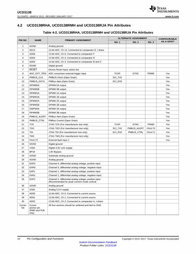
4.2 UCD3138RHA, UCD3138RMH and UCD3138RJA Pin Attributes
Table 4-2. UCD3138RHA, UCD3138RMH and UCD3138RJA Pin Attributes
PIN NO. NAME PRIMARY ASSIGNMENTALTERNATE ASSIGNMENT CONFIGURABLE
AS A GPIO?NO. 1 NO. 2 NO. 3
1 AGND Analog ground
2 AD13 12-bit ADC, Ch 13, Connected to comparator E, I-share
3 AD06 12-bit ADC, Ch 6, Connected to comparator F
4 AD04 12-bit ADC, Ch 4, Connected to comparator D
5 AD03 12-bit ADC, Ch 3, Connected to comparator B and C
6 DGND Digital ground
7 RESET Device Reset Input, active low
8 ADC_EXT_TRIG ADC conversion external trigger input TCAP SYNC PWM0 Yes
9 PMBUS_CLK PMBUS Clock (Open Drain) SCI_TX0 Yes
10 PMBUS_DATA PMBus data (Open Drain) SCI_RX0 Yes
11 DPWM0A DPWM 0A output Yes
12 DPWM0B DPWM 0B output Yes
13 DPWM1A DPWM 1A output Yes
14 DPWM1B DPWM 1B output Yes
15 DPWM2A DPWM 2A output Yes
16 DPWM2B DPWM 2B output Yes
17 DWPM3A DPWM 3A output Yes
18 DPWM3B DPWM 3B output Yes
19 PMBUS_ALERT PMBus Alert (Open Drain) Yes
20 PMBUS_CTRL PMBus Control (Open Drain) Yes
21 TCK JTAG TCK (For manufacturer test only) TCAP SYNC PWM0 Yes
22 TDO JTAG TDO (For manufacturer test only) SCI_TX0 PMBUS_ALERT FAULT0 Yes
23 TDI JTAG TDI (For manufacturer test only) SCI_RX0 PMBUS_CTRL FAULT1 Yes
24 TMS JTAG TMS (For manufacturer test only) Yes
25 FAULT2 External fault input 2 Yes
26 DGND Digital ground
27 V33D Digital 3.3V core supply
28 BP18 1.8V Bypass
29 AGND Substrate analog ground
30 AGND Analog ground
31 EAP0 Channel 0, differential analog voltage, positive input
32 EAN0 Channel 0, differential analog voltage, negative input
33 EAP1 Channel 1, differential analog voltage, positive input
34 EAN1 Channel 1, differential analog voltage, negative input
35 EAP2 Channel 2, differential analog voltage, positive input(Recommended for peak currrent mode control)
36 AGND Analog ground
37 V33A Analog 3.3-V supply
38 AD00 12-bit ADC, Ch 0, Connected to current source
39 AD01 12-bit ADC, Ch 1, Connected to current source
40 AD02 12-bit ADC, Ch 2, Connected to comparator A, I-share
CornerNA
Corneranchor pin(RMH and RJAonly)
All four anchors should be soldered and tied to GND

13
UCD3138www.ti.com SLUSAP2I –MARCH 2012–REVISED JANUARY 2017
Submit Documentation FeedbackProduct Folder Links: UCD3138
SpecificationsCopyright © 2012–2017, Texas Instruments Incorporated
(1) Stresses beyond those listed under Absolute Maximum Ratings may cause permanent damage to the device. These are stress ratingsonly, and functional operation of the device at these or any other conditions beyond those indicated under Recommended OperatingConditions is not implied. Exposure to absolute-maximum-rated conditions for extended periods may affect device reliability.
(2) Referenced to DGND
5 Specifications
5.1 Absolute Maximum Ratings (1)
over operating free-air temperature range (unless otherwise noted)MIN MAX UNIT
V33D V33D to DGND –0.3 3.8 VV33DIO V33DIO to DGND –0.3 3.8 VV33A V33A to AGND –0.3 3.8 VBP18 BP18 to DGND –0.3 2.5 V|DGND – AGND| Ground difference 0.3 VAll pins, excludingAGND (2) Voltage applied to any pin –0.3 3.8 V
TJ Junction temperature –40 150 °CTstg Storage temperature –55 150 °C
(1) JEDEC document JEP155 states that 500-V HBM allows safe manufacturing with a standard ESD control process.(2) JEDEC document JEP157 states that 250-V CDM allows safe manufacturing with a standard ESD control process.
5.2 ESD RatingsVALUE UNIT
V(ESD) Electrostatic dischargeHuman-body model (HBM), per ANSI/ESDA/JEDEC JS-001 (1) ±2000
VCharged-device model (CDM), per JEDEC specification JESD22-C101 (2) ±500
5.3 Recommended Operating Conditionsover operating free-air temperature range (unless otherwise noted)
MIN NOM MAX UNITV33D Digital power 3.0 3.3 3.6 VV33DIO Digital I/O power 3.0 3.3 3.6V33A Analog power 3.0 3.3 3.6 VTJ Junction temperature –40 125 °CBP18 1.8-V digital power 1.6 1.8 2.0 V
(1) For more information about traditional and new thermal metrics, see Semiconductor and IC Package Thermal Metrics application report.
5.4 Thermal Information
THERMAL METRIC (1)UCD3138 UCD3138 UCD3138 UCD3138
UNIT64 PIN QFN(RGC)
40 PIN QFN(RHA)
40 PIN QFN(RMH)
40 PIN QFN(RJA)
RθJA Junction-to-ambient thermal resistance 25.1 31.8 31.0 30.1 °C/WRθJC(top) Junction-to-case (top) thermal resistance 10.5 18.5 16.5 13.5 °C/WRθJB Junction-to-board thermal resistance 4.6 6.8 6.3 4.9 °C/WψJT Junction-to-top characterization parameter 0.2 0.2 0.2 0.2 °C/WψJB Junction-to-board characterization parameter 4.6 6.7 6.3 4.8 °C/WRθJC(bot) Junction-to-case (bottom) thermal resistance 1.2 1.8 1.1 0.7 °C/W

14
UCD3138SLUSAP2I –MARCH 2012–REVISED JANUARY 2017 www.ti.com
Submit Documentation FeedbackProduct Folder Links: UCD3138
Specifications Copyright © 2012–2017, Texas Instruments Incorporated
(1) As designed and characterized. Not 100% tested in production.
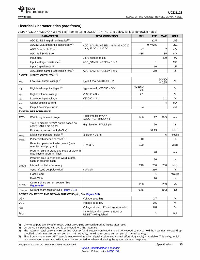
5.5 Electrical CharacteristicsV33A = V33D = V33DIO = 3.3 V; 1 μF from BP18 to DGND, TJ = –40°C to 125°C (unless otherwise noted)
PARAMETER TEST CONDITION MIN TYP MAX UNITSUPPLY CURRENT
I33AMeasured on V33A. The device ispowered up but all ADC12 and EADCsampling is disabled
6.3 mA
I33DIO All GPIO and communication pins areopen 0.35 mA
I33D ROM program execution 60 mAI33D Flash programming in ROM mode 70 mA
I33The device is in ROM mode with allDPWMs enabled and switching at 2MHz. The DPWMs are all unloaded.
100 mA
ERROR ADC INPUTS EAP, EANEAP – AGND –0.15 1.998 VEAP – EAN –0.256 1.848 VTypical error range AFE = 0 –256 248 mV
EAP – EAN Error voltage digital resolution
AFE = 3 0.8 1 1.20 mVAFE = 2 1.7 2 2.30 mVAFE = 1 3.55 4 4.45 mVAFE = 0 6.90 8 9.10 mV
REA Input impedance (See Figure 5-4) AGND reference 0.5 MΩIOFFSET Input offset current (See Figure 5-4) –5 5 μA
EADC offset
Input voltage = 0 V at AFE = 0 –2 2 LSBInput voltage = 0 V at AFE = 1 –2.5 2.5 LSBInput voltage = 0 V at AFE = 2 –3 -3 LSBInput voltage = 0 V at AFE = 3 –4 4 LSB
Sample Rate 16 MHzAnalog Front End Amplifier Bandwidth 100 MHz
A0Gain See Figure 5-5 1 V/VMinimum output voltage 100 mV
EADC DACDAC range 0 1.6 VVREF DAC reference resolution 10 bit, No dithering enabled 1.56 mVVREF DAC reference resolution With 4 bit dithering enabled 97.6 μVINL –3.0 3.0 LSBDNL Does not include MSB transition –2.1 1.6 LSBDNL at MSB transition –1.4 LSBDAC reference voltage 1.58 1.61 V
τ Settling Time From 10% to 90% 250 nsADC12IBIAS Bias current for PMBus address pins 9.5 10.5 μA
Measurement range for voltage monitoring 0 2.5 VInternal ADC reference voltage –40°C to 125°C 2.475 2.500 2.525 V
Change in Internal ADC reference from25°C reference voltage (1)
–40°C to 25°C –0.4mV25°C to 85°C –1.8
25°C to 125°C –4.2
15
UCD3138www.ti.com SLUSAP2I –MARCH 2012–REVISED JANUARY 2017
Submit Documentation FeedbackProduct Folder Links: UCD3138
SpecificationsCopyright © 2012–2017, Texas Instruments Incorporated
Electrical Characteristics (continued)V33A = V33D = V33DIO = 3.3 V; 1 μF from BP18 to DGND, TJ = –40°C to 125°C (unless otherwise noted)
PARAMETER TEST CONDITION MIN TYP MAX UNIT
(2) DPWM outputs are low after reset. Other GPIO pins are configured as inputs after reset.(3) On the 40-pin package V33DIO is connected to V33D internally.(4) The maximum total current, IOHmax and IOLmax for all outputs combined, should not exceed 12 mA to hold the maximum voltage drop
specified. Maximum sink current per pin = –6 mA at VOL; maximum source current per pin = 6 mA at VOH.(5) Time from close of error ADC sample window to time when digitally calculated control effort (duty cycle) is available. This delay, which
has no variation associated with it, must be accounted for when calculating the system dynamic response.
ADC12 INL integral nonlinearity (1)
ADC_SAMPLINGSEL = 6 for all ADC12data, 25 °C to 125 °C
±2.5 LSBADC12 DNL differential nonlinearity (1) –0.7/+2.5 LSBADC Zero Scale Error –7 7 mVADC Full Scale Error –35 35 mVInput bias 2.5 V applied to pin 400 nAInput leakage resistance (1) ADC_SAMPLINGSEL= 6 or 0 1 MΩInput Capacitance (1) 10 pFADC single sample conversion time (1) ADC_SAMPLINGSEL= 6 or 0 3.9 μs
DIGITAL INPUTS/OUTPUTS (2) (3)
VOL Low-level output voltage (4) IOH = 4 mA, V33DIO = 3 V DGND+ 0.25 V
VOH High-level output voltage (4) IOH = –4 mA, V33DIO = 3 V V33DIO– 0.6 V
VIH High-level input voltage V33DIO = 3 V 2.1 VVIL Low-level input voltage V33DIO = 3 V 1.1 VIOH Output sinking current 4 mAIOL Output sourcing current –4 mASYSTEM PERFORMANCE
TWD Watchdog time out range Total time is: TWD ×(WDCTRL.PERIOD + 1) 14.6 17 20.5 ms
Time to disable DPWM output based onactive FAULT pin signal High level on FAULT pin 70 ns
Processor master clock (MCLK) 31.25 MHztDelay Digital compensator delay (5) (1 clock = 32 ns) 6 clockst(reset) Pulse width needed at reset (1) 10 µs
Retention period of flash content (dataretention and program) TJ = 25°C 100 years
Program time to erase one page or block indata flash or program flash 20 ms
Program time to write one word in dataflash or program flash 20 µs
f(PCLK) Internal oscillator frequency 240 250 260 MHzSync-in/sync-out pulse width Sync pin 256 nsFlash Read 1 MCLKsFlash Write 20 μs
ISHARECurrent share current source (SeeFigure 6-16) 238 259 μA
RSHARE Current share resistor (See Figure 6-16) 9.75 10.3 kΩPOWER ON RESET AND BROWN OUT (V33D pin, See Figure 5-3)VGH Voltage good high 2.7 VVGL Voltage good low 2.5 VVres Voltage at which IReset signal is valid 0.8 V
TPORTime delay after power is good orRESET* relinquished 1 ms

16
UCD3138SLUSAP2I –MARCH 2012–REVISED JANUARY 2017 www.ti.com
Submit Documentation FeedbackProduct Folder Links: UCD3138
Specifications Copyright © 2012–2017, Texas Instruments Incorporated
Electrical Characteristics (continued)V33A = V33D = V33DIO = 3.3 V; 1 μF from BP18 to DGND, TJ = –40°C to 125°C (unless otherwise noted)
PARAMETER TEST CONDITION MIN TYP MAX UNIT
(6) Characterized by design and not production tested.(7) Ambient temperature offset value should be used from the TEMPSENCTRL register to meet accuracy.(8) Available from reference DACs for comparators D, E, F, and G.
Brownout Internal signal warning of brownoutconditions 2.9 V
TEMPERATURE SENSOR (6)
VTEMP Voltage range of sensor 1.46 2.44 VVoltage resolution V/°C 5.9 mV/ºCTemperature resolution °C per bit 0.1034 ºC/LSBAccuracy (6) (7) –40°C to 125°C –10 ±5 10 ºCTemperature range –40°C to 125°C –40 125 ºC
ITEMP Current draw of sensor when active 30 μATON Turn on time / settling time of sensor 100 μsVAMB Ambient temperature Trimmed 25°C reading 1.85 VANALOG COMPARATORDAC Reference DAC Range 0 2.5 V
Reference Voltage 2.478 2.5 2.513 VBits 7 bitsINL (6) –0.42 0.21 LSBDNL (6) 0.06 0.12 LSBOffset –5.5 19.5 mVTime to disable DPWM output based on 0V to 2.5 V step input on the analogcomparator. (1)
150 ns
Reference DAC buffered output load (8) 0.5 1 mABuffer offset (–0.5 mA) 4.6 8.3 mVBuffer offset (1.0 mA) –0.05 17 mV
(1) Fast mode, 400 kHz(2) The device times out when any clock low exceeds t(TIMEOUT).
5.6 Timing and Switching CharacteristicsThe timing characteristics and timing diagram for the communications interface that supports I2C, SMBus,and PMBus in Slave or Master mode are shown in Table 5-1, Figure 5-1, and Figure 5-2. The numbers inTable 5-1 arµe for 400 kHz operating frequency. However, the device supports all three speeds, standard(100 kHz), fast (400 kHz), and fast mode plus (1 MHz).
Table 5-1. PMBus/SMBus/I2C Timing
PARAMETER TEST CONDITIONS MIN TYP MAX UNITTypical values at TA = 25°C and VCC = 3.3 V (unless otherwise noted)fSMB SMBus/PMBus operating frequency Slave mode, SMBC 50% duty cycle 100 1000 kHzfI2C I2C operating frequency Slave mode, SCL 50% duty cycle 100 1000 kHz
t(BUF)Bus free time between start andstop (1) 1.3 µs
t(HD:STA) Hold time after (repeated) start (1) 0.6 µst(SU:STA) Repeated start setup time (1) 0.6 µst(SU:STO) Stop setup time (1) 0.6 µst(HD:DAT) Data hold time Receive mode 0 nst(SU:DAT) Data setup time 100 nst(TIMEOUT) Error signal/detect (2) 35 ms

17
UCD3138www.ti.com SLUSAP2I –MARCH 2012–REVISED JANUARY 2017
Submit Documentation FeedbackProduct Folder Links: UCD3138
SpecificationsCopyright © 2012–2017, Texas Instruments Incorporated
Table 5-1. PMBus/SMBus/I2C Timing (continued)PARAMETER TEST CONDITIONS MIN TYP MAX UNIT
(3) t(HIGH), Max, is the minimum bus idle time. SMBC = SMBD = 1 for t > 50 ms causes reset of any transaction that is in progress. Thisspecification is valid when the NC_SMB control bit remains in the default cleared state (CLK[0] = 0).
(4) t(LOW:SEXT) is the cumulative time a slave device is allowed to extend the clock cycles in one message from initial start to the stop.(5) Cb (pF)
t(LOW) Clock low period 1.3 µst(HIGH) Clock high period (3) 0.6 µs
t(LOW:SEXT)Cumulative clock low slave extendtime (4) 25 ms
tf Clock/data fall time Rise time tr = (VILmax – 0.15) to (VIHmin + 0.15) 20 + 0.1Cb (5) 300 ns
tr Clock/data rise time Fall time tf = 0.9 VDD to (VILmax – 0.15) 20 + 0.1Cb (5) 300 ns
Cb Total capacitance of one bus line 400 pF
Figure 5-1. I2C/SMBus/PMBus Timing Diagram
Figure 5-2. Bus Timing in Extended Mode
5.7 Power Supply Sequencing

TPOR
undefined
V33D
IReset
3.3 V
TPOR
VGH
VGL
Vres
t
t
Brown Out
18
UCD3138SLUSAP2I –MARCH 2012–REVISED JANUARY 2017 www.ti.com
Submit Documentation FeedbackProduct Folder Links: UCD3138
Specifications Copyright © 2012–2017, Texas Instruments Incorporated
Figure 5-3. Power-On Reset (POR) and Brown-Out Reset (BOR)
Table 5-2. Power-On Reset (POR) and Brown-Out Reset (BOR) Term Definitions
TERM DEFINITION
VGH This is the V33D threshold where the internal power is declared good. The UCD3138 comes out of reset when abovethis threshold.
VGL This is the V33D threshold where the internal power is declared bad. The device goes into reset when below thisthreshold.
VresThis is the V33D threshold where the internal reset signal is no longer valid. Below this threshold the device is in anindeterminate state.
IResetThis is the internal reset signal. When low, the device is held in reset. This is equivalent to holding the reset pin onthe IC high.
TPOR The time delay from when VGH is exceeded to when the device comes out of reset.
Brown out This is the V33D voltage threshold at which the device sets the brown out status bit. In addition an interrupt can betriggered if enabled.
5.8 Peripherals
5.8.1 Digital Power Peripherals (DPPs)At the core of the UCD3138 controller are three DDPs. Each DPP can be configured to drive from one toeight DPWM outputs. Each DPP consists of:• Differential input error ADC (EADC) with sophisticated controls• Hardware accelerated digital 2-pole/2-zero PID based compensator• Digital PWM module with support for a variety of topologies
These can be connected in many different combinations, with multiple filters and DPWMs. They arecapable of supporting functions like input voltage feed forward, current mode control, and constantcurrent/constant power, and so forth. The simplest configuration is shown in the following figure:

IOFFSETREA
EAP
EAN
AGND
AGND
IOFFSETREA
Front End Differential
Amplifier
Error ADC(Front End)
FilterDigitalPWM
EAP
EAN
DPWMA
DPWMB
19
UCD3138www.ti.com SLUSAP2I –MARCH 2012–REVISED JANUARY 2017
Submit Documentation FeedbackProduct Folder Links: UCD3138
SpecificationsCopyright © 2012–2017, Texas Instruments Incorporated
5.8.1.1 Front End
Figure 5-4 shows the block diagram of the front end module. It consists of a differential amplifier, anadjustable gain error amplifier, a high speed flash analog to digital converter (EADC), digital averagingfilters and a precision high resolution set point DAC reference. The programmable gain amplifier in concertwith the EADC and the adjustable digital gain on the EADC output work together to provide 9 bits of rangewith 6 bits of resolution on the EADC output. The output of the Front End module is a 9-bit sign extendedresult with a gain of 1 LSB / mV. Depending on the value of AFE selected, the resolution of this outputcould be either 1, 2, 4 or 8 LSBs. In addition Front End 0 has the ability to automatically select the AFEvalue such that the minimum resolution is maintained that still allows the voltage to fit within the range ofthe measurement. The EADC control logic receives the sample request from the DPWM module forinitiating an EADC conversion. EADC control circuitry captures the EADC-9-bit-code and strobes thedigital compensator for processing of the representative error. The set point DAC has 10 bits with anadditional 4 bits of dithering resulting in an effective resolution of 14 bits. This DAC can be driven from avariety of sources to facilitate things like soft start, nested loops, and so forth. Some additional featuresinclude the ability to change the polarity of the error measurement and an absolute value mode whichautomatically adds the DAC value to the error.
It is possible to operate the controller in a peak current mode control configuration; front-end 2 isrecommended for implementing peak current mode control. In this mode topologies like the phase shiftedfull bridge converter can be controlled to maintain transformer flux balance. The internal DAC can beramped at a synchronously controlled slew rate to achieve a programmable slope compensation. Thiseliminates the sub-harmonic oscillation as well as improves input voltage feed-forward performance. A0 isa unity gain buffer used to isolate the peak current mode comparator. The offset of this buffer is specifiedin Section 5.5.
Figure 5-4. Input Stage of EADC Module

EAP0
EAN0
DAC0
EADC
4 bit dithering gives 14 bits of effective resolution
97.65625 µV/LSB effective resolution
X
6 bit ADC
8 mV/LSB
Signed 9 bit result
(error) 1 mV /LSB
AFE_GAIN
10 bit DAC
1.5625 mV/LSB Value
Dither
S
CPCC
Filter x
Ramp
SAR/Prebias
Absolute Value
Calculation
Averaging
10 bit result
1.5625 mV/LSB
23-AFE_GAIN
Peak Current Mode
Comparator
Peak Current
Detected
A0
2AFE_GAIN
20
UCD3138SLUSAP2I –MARCH 2012–REVISED JANUARY 2017 www.ti.com
Submit Documentation FeedbackProduct Folder Links: UCD3138
Specifications Copyright © 2012–2017, Texas Instruments Incorporated
Figure 5-5. Front End Module(Front End 2 Recommended for Peak Current Mode Control)
5.8.1.2 DPWM Module
The DPWM module represents one complete DPWM channel with 2 independent outputs, A and B.Multiple DPWM modules within the UCD3138 system can be configured to support all key powertopologies. DPWM modules can be used as independent DPWM outputs, each controlling one powersupply output voltage rail. It can also be used as a synchronized DPWM—with user selectable phase shiftbetween the DPWM channels to control power supply outputs with multiphase or interleaved DPWMconfigurations.
The output of the filter feeds the high resolution DPWM module. The DPWM module produces the pulsewidth modulated outputs for the power stage switches. The compensator calculates the necessary dutyratio as a 24-bit number in Q23 fixed point format (23 bit integer with 1 sign bit). This represents a valuewithin the range 0.0 to 1.0. This duty ratio value is used to generate the corresponding DPWM output ONtime. The resolution of the DPWM ON time is 250 psec.
Each DPWM module can be synchronized to another module or to an external sync signal. An inputSYNC signal causes a DPWM ramp timer to reset. The SYNC signal outputs—from each of the fourDPWM modules—occur when the ramp timer crosses a programmed threshold. In this way the phase ofthe DPWM outputs for multiple power stages can be tightly controlled.
The DPWM logic is probably the most complex of the Digital Peripherals. It takes the output of thecompensator and converts it into the correct DPWM output for several power supply topologies. Itprovides for programmable dead times and cycle adjustments for current balancing between phases. Itcontrols the triggering of the EADC. It can synchronize to other DPWMs or to external sources. It canprovide synchronization information to other DPWMs or to external recipients. In addition, it interfaces toseveral fault handling circuits. Some of the control for these fault handling circuits is in the DPWMregisters. Fault handling is covered in the Fault Mux section.
Each DPWM module supports the following features:• Dedicated 14 bit time-base with period and frequency control• Shadow period register for end of period updates.• Quad-event control registers (A and B, rising and falling) (Events 1 to 4)
– Used for on/off DPWM duty ratio updates.

21
UCD3138www.ti.com SLUSAP2I –MARCH 2012–REVISED JANUARY 2017
Submit Documentation FeedbackProduct Folder Links: UCD3138
SpecificationsCopyright © 2012–2017, Texas Instruments Incorporated
• Phase control relative to other DPWM modules• Sample trigger placement for output voltage sensing at any point during the DPWM cycle.• Support for two independent edge placement DPWM outputs (same frequency or period setting)• Dead-time between DPWM A and B outputs• High Resolution capabilities – 250 ps• Pulse cycle adjustment of up to ±8.192 µs (32768 × 250 ps)• Active high/ active low output polarity selection• Provides events to trigger both CPU interrupts and start of ADC12 conversions.
5.8.1.3 DPWM Events
Each DPWM can control the following timing events:1. Sample Trigger Count–This register defines where the error voltage is sampled by the EADC in
relationship to the DPWM period. The programmed value set in the register should be one fourth of thevalue calculated based on the DPWM clock. As the DCLK (DCLK = 62.5 MHz max) controlling thecircuitry runs at one fourth of the DPWM clock (PCLK = 250 MHz max). When this sample triggercount is equal to the DPWM Counter, it initiates a front end calculation by triggering the EADC,resulting in a CLA calculation, and a DPWM update. Oversampling can be set for 2, 4, or 8 times thesampling rate.
2. Phase Trigger Count – count offset for slaving another DPWM (Multi-Phase/Interleaved operation).3. Period – low resolution switching period count. (count of PCLK cycles)4. Event 1 – count offset for rising DPWM A event. (PCLK cycles)5. Event 2 – DPWM count for falling DPWM A event that sets the duty ratio. Last 4 bits of the register are
for high resolution control. Upper 14 bits are the number of PCLK cycle counts.6. Event 3 – DPWM count for rising DPWM B event. Last 4 bits of the register are for high resolution
control. Upper 14 bits are the number of PCLK cycle counts.7. Event 4 – DPWM count for falling DPWM B event. Last 4 bits of the register are for high resolution
control. Upper 14 bits are the number of PCLK cycle counts.8. Cycle Adjust – Constant offset for Event 2 and Event 4 adjustments.
Basic comparisons between the programmed registers and the DPWM counter can create the desirededge placements in the DPWM. High resolution edge capability is available on Events 2, 3, and 4.
Figure 5-6 is for multi-mode, open loop. Open loop means that the DPWM is controlled entirely by its ownregisters, not by the filter output. In other words, the power supply control loop is not closed.
The Sample Trigger signals are used to trigger the front end to sample input signals. The Blanking signalsare used to blank fault measurements during noisy events, such as FET turn on and turn off. AdditionalDPWM modes are described below.

Start of Period
Period Counter
Start of Period
Period
Sample Trigger 1
DPWM Output A
Cycle Adjust A (High Resolution)
Event 2 (High Resolution)
Event 1
Event 3 (High Resolution)
Cycle Adjust B (High Resolution)
Event 4 (High Resolution)
DPWM Output B
Blanking A Begin
Blanking A End
Blanking B Begin
Blanking B End
Phase Trigger
Sample Trigger 2
To Other
Modules
To Other
Modules
Multi Mode Open Loop
Events which change with DPWM mode:
DPWM A Rising Edge = Event 1
DPWM A Falling Edge = Event 2 + Cycle Adjust A
DPWM B Rising Edge = Event 3
DPWM B Falling Edge = Event 4 + Cycle Adjust B
Phase Trigger = Phase Trigger Register value
Events always set by their registers, regardless of mode:
Sample Trigger 1, Sample Trigger 2, Blanking A Begin, Blanking A End, Blanking B Begin,
Blanking B End
22
UCD3138SLUSAP2I –MARCH 2012–REVISED JANUARY 2017 www.ti.com
Submit Documentation FeedbackProduct Folder Links: UCD3138
Specifications Copyright © 2012–2017, Texas Instruments Incorporated
Figure 5-6. Multi Mode Open Loop
5.8.1.4 High Resolution DPWM
Unlike conventional PWM controllers where the frequency of the clock dictates the maximum resolution ofPWM edges, the UCD3138 DPWM can generate waveforms with resolutions as small as 250 ps. This is16× the resolution of the clock driving the DPWM module.
23
UCD3138www.ti.com SLUSAP2I –MARCH 2012–REVISED JANUARY 2017
Submit Documentation FeedbackProduct Folder Links: UCD3138
SpecificationsCopyright © 2012–2017, Texas Instruments Incorporated
This is achieved by providing the DPWM mechanism with 16 phase shifted clock signals of 250 MHzeach. The high resolution section of DPWM can be enabled or disabled, also the resolution can be definedin several steps between 4ns to 250ps. This is done by setting the values of PWM_HR_MULTI_OUT_EN,HIRES_SCALE, and ALL_PHASE_CLK_ENA inside the DPWM Control register 1. See the PowerPeripherals programmer’s manual for details.
5.8.1.5 Oversampling
The DPWM module has the capability to trigger an oversampling event by initiating the EADC to samplethe error voltage. The default 00 configuration has the DPWM trigger the EADC once based on thesample trigger register value. The over sampling register has the ability to trigger the sampling 2, 4 or 8times per PWM period. Thus the time the over sample happens is at the divide by 2, 4, or 8 time set in thesampling register. The 01 setting triggers 2X oversampling, the 10 setting triggers 4X over sampling, andthe 11 triggers oversampling at 8X.
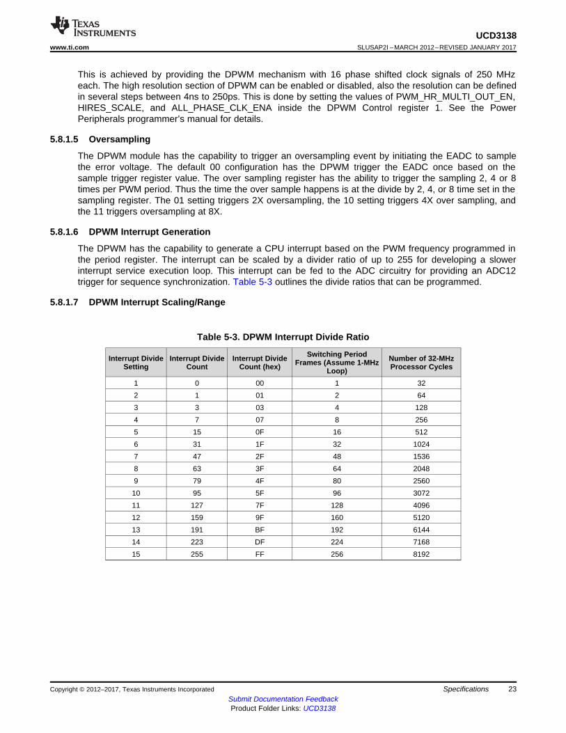
5.8.1.6 DPWM Interrupt Generation
The DPWM has the capability to generate a CPU interrupt based on the PWM frequency programmed inthe period register. The interrupt can be scaled by a divider ratio of up to 255 for developing a slowerinterrupt service execution loop. This interrupt can be fed to the ADC circuitry for providing an ADC12trigger for sequence synchronization. Table 5-3 outlines the divide ratios that can be programmed.
5.8.1.7 DPWM Interrupt Scaling/Range
Table 5-3. DPWM Interrupt Divide Ratio
Interrupt DivideSetting
Interrupt DivideCount
Interrupt DivideCount (hex)
Switching PeriodFrames (Assume 1-MHz
Loop)Number of 32-MHzProcessor Cycles
1 0 00 1 322 1 01 2 643 3 03 4 1284 7 07 8 2565 15 0F 16 5126 31 1F 32 10247 47 2F 48 15368 63 3F 64 20489 79 4F 80 256010 95 5F 96 307211 127 7F 128 409612 159 9F 160 512013 191 BF 192 614414 223 DF 224 716815 255 FF 256 8192
1.92
1.96
2
2.04
2.08
−40 −20 0 20 40 60 80 100 120
Temperature (°C)
2-M
HZ
Re
fere
nce
G004b
UCD3138 Oscillator Frequency
−4
−2
0
2
4
6
8
−40 −20 0 20 40 60 80 100 120
Temperature (°C)
AD
C12 E
rror
(LS
B)
G002b
ADC12 Temperature Sensor Measurement Error
2.475
2.480
2.485
2.490
2.495
2.500
2.505
2.510
2.515
−40 −20 0 20 40 60 80 100 120
Temperature (°C)
AD
C1
2 R
efe
ren
ce
G003b
ADC12 2.5-V Reference
1.4
1.6
1.8
2.0
2.2
2.4
2.6
−60 −40 −20 0 20 40 60 80 100 120 140 160
Temperature (°C)
Sensor
Voltage (
V)
G006b
ADC12 Measurement Temperature Sensor Voltage
1.71
1.73
1.75
1.77
1.79
1.81
-50 0 50 100 150
Vol
tage
(V
)
Temperature (C)
Minimum
Maximum
Typical
C001
1.6
1.7
1.8
1.9
2
2.1
−40 −20 0 20 40 60 80 100 120
Temperature (°C)
EA
DC
LS
B S
ize (
mV
)
G005a
24
UCD3138SLUSAP2I –MARCH 2012–REVISED JANUARY 2017 www.ti.com
Submit Documentation FeedbackProduct Folder Links: UCD3138
Specifications Copyright © 2012–2017, Texas Instruments Incorporated
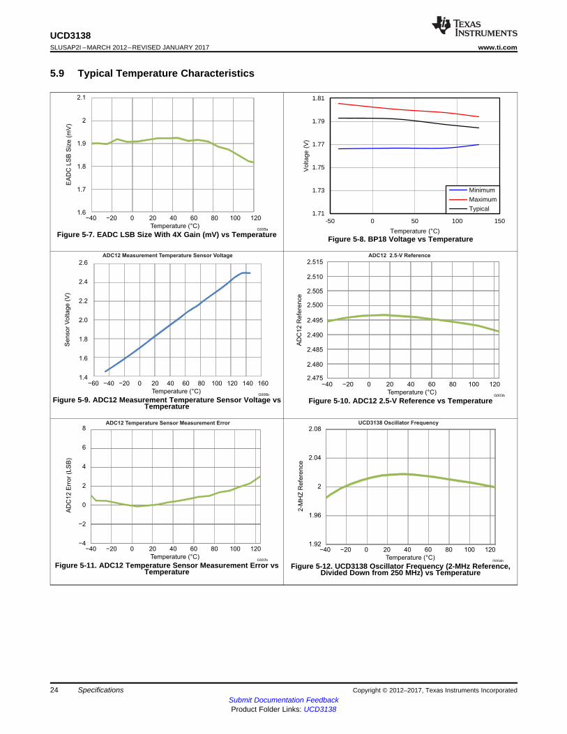
5.9 Typical Temperature Characteristics
Figure 5-7. EADC LSB Size With 4X Gain (mV) vs Temperature Figure 5-8. BP18 Voltage vs Temperature
Figure 5-9. ADC12 Measurement Temperature Sensor Voltage vsTemperature
Figure 5-10. ADC12 2.5-V Reference vs Temperature
Figure 5-11. ADC12 Temperature Sensor Measurement Error vsTemperature
Figure 5-12. UCD3138 Oscillator Frequency (2-MHz Reference,Divided Down from 250 MHz) vs Temperature

25
UCD3138www.ti.com SLUSAP2I –MARCH 2012–REVISED JANUARY 2017
Submit Documentation FeedbackProduct Folder Links: UCD3138
Detailed DescriptionCopyright © 2012–2017, Texas Instruments Incorporated
6 Detailed Description
6.1 OverviewThe UCD3138 family is a digital power supply controller from Texas Instruments offering superior levels ofintegration and performance in a single chip solution. The UCD3138x, in comparison to Texas InstrumentsUCD3138 digital power controller offers 32 kB of program Flash memory. The flexible nature of theUCD3138 family makes it suitable for a wide variety of power conversion applications.
In addition, multiple peripherals inside the device have been specifically optimized to enhance theperformance of AC/DC and isolated DC/DC applications and reduce the solution component count in theIT and network infrastructure space. The UCD3138 family is a fully programmable solution offeringcustomers complete control of their application, along with ample ability to differentiate their solution. Atthe same time, TI is committed to simplifying our customer’s development effort through offering best inclass development tools, including application firmware, Code Composer StudioTM software developmentenvironment, and TI’s Fusion Power Development GUI which enables customers to configure and monitorkey system parameters.
6.2 ARM Processor
The ARM7TDMI-S processor is a synthesizable member of the ARM family of general purpose 32-bitmicroprocessors. The ARM architecture is based on RISC (Reduced Instruction Set Computer) principleswhere two instruction sets are available. The 32-bit ARM instruction set and the 16-bit Thumb instructionset. The Thumb instruction allows for higher code density equivalent to a 16-bit microprocessor, with theperformance of the 32-bit microprocessor.
The three-staged pipelined ARM processor has fetch, decode and execute stage architecture. Majorblocks in the ARM processor include a 32-bit ALU, 32 x 8 multiplier, and a barrel shifter.
6.3 MemoryThe UCD3138 (ARM7TDMI-S) is a Von-Neumann architecture, where a single bus provides access to allof the memory modules. All of the memory module addresses are sequentially aligned along the sameaddress range. This applies to program flash, data flash, ROM and all other peripherals.
Within the UCD3138 architecture, there is a Boot ROM that contains the initial firmware startup routinesfor PMBUS communication and non-volatile (FLASH) memory download. This boot ROM is executed afterpower-up-reset checks if there is a valid FLASH program written. If a valid program is present, the ROMcode branches to the main FLASH-program execution.
UCD3138 also supports customization of the boot program by allowing an alternative boot routine to beexecuted from program FLASH. This feature enables assignment of a unique address to each device;therefore, enabling firmware reprogramming even when several devices are connected on the samecommunication bus.
Two separate FLASH memory areas are present inside the device. The 32 kB Program FLASH isorganized as an 8 k x 32 bit memory block and is intended to be for the firmware program. The block isconfigured with page erase capability for erasing blocks as small as 1kB per page, or with a mass erasefor erasing the entire program FLASH array. The FLASH endurance is specified at 1000 erase/writecycles and the data retention is good for 100 years. The 2 kB data FLASH array is organized as a 512 x32 bit memory (32 byte page size). The Data FLASH is intended for firmware data value storage and datalogging. Thus, the Data FLASH is specified as a high endurance memory of 20 k cycles with embeddederror correction code (ECC).
For run time data storage and scratchpad memory, a 4 kB RAM is available. The RAM is organized as a 1k x 32 bit array.

26
UCD3138SLUSAP2I –MARCH 2012–REVISED JANUARY 2017 www.ti.com
Submit Documentation FeedbackProduct Folder Links: UCD3138
Detailed Description Copyright © 2012–2017, Texas Instruments Incorporated
6.3.1 CPU Memory Map and InterruptsWhen the device comes out of power-on-reset, the data memories are mapped to the processor asfollows:
Table 6-1. Memory Map (After Reset Operation)
Address Size Module0x0000_0000 – 0x0000_FFFFIn 16 repeated blocks of 4K each 16 X 4K Boot ROM
0x0001_0000 – 0x0001_7FFF 32K Program flash0x0001_8800 – 0x0001_8FFF 2K Data flash0x0001_9000 – 0x0001_9FFF 4K Data RAM
Just before the boot ROM program gives control to FLASH program, the ROM configures the memory asfollows:
Table 6-2. Memory Map (Normal Operation)
Address Size Module0x0000_0000 – 0x0000_7FFF 32K Program flash0x0001_0000 – 0x0001_AFFF 4K Boot ROM0x0001_8800 – 0x0001_8FFF 2K Data flash0x0001_9000 – 0x0001_9FFF 4K Data RAM
Table 6-3. Memory Map (System and Peripherals Blocks)
Address Size Module0x0002_0000 - 0x0002_00FF 256 Loop Mux0x0003_0000 - 0x0003_00FF 256 Fault Mux0x0004_0000 - 0x0004_00FF 256 ADC0x0005_0000 - 0x0005_00FF 256 DPWM 30x0006_0000 - 0x0006_00FF 256 Filter 20x0007_0000 - 0x0007_00FF 256 DPWM 20x0008_0000 - 0x0008_00FF 256 Front End/Ramp I/F 20x0009_0000 - 0x0009_00FF 256 Filter 10x000A_0000 - 0x000A_00FF 256 DPWM 10x000B_0000 – 0x000B_00FF 256 Front End/Ramp I/F 10x000C_0000 - 0x000C_00FF 256 Filter 00x000D_0000 - 0x000D_00FF 256 DPWM 00x000E_0000 - 0x000E_00FF 256 Front End/Ramp I/F 00xFFF7_EC00 - 0xFFF7_ECFF 256 UART 00xFFF7_ED00 - 0xFFF7_EDFF 256 UART 10xFFF7_F000 - 0xFFF7_F0FF 256 Miscellaneous Analog Control0xFFF7_F600 - 0xFFF7_F6FF 256 PMBus Interface0xFFF7_FA00 - 0xFFF7_FAFF 256 GIO0xFFF7_FD00 - 0xFFF7_FDFF 256 Timer0xFFFF_FD00 - 0xFFFF_FDFF 256 MMC0xFFFF_FE00 - 0xFFFF_FEFF 256 DEC0xFFFF_FF20 - 0xFFFF_FF37 23 CIM0xFFFF_FF40 - 0xFFFF_FF50 16 PSA0xFFFF_FFD0 - 0xFFFF_FFEC 28 SYS

27
UCD3138www.ti.com SLUSAP2I –MARCH 2012–REVISED JANUARY 2017
Submit Documentation FeedbackProduct Folder Links: UCD3138
Detailed DescriptionCopyright © 2012–2017, Texas Instruments Incorporated
The registers and bit definitions inside the system and peripheral blocks are detailed in the programmer’sguide for each peripheral.
6.3.2 Boot ROMThe UCD3138 incorporates a 4k boot ROM. This boot ROM includes support for:• Program download through the PMBus• Device initialization• Examining and modifying registers and memory• Verifying and executing program FLASH automatically• Jumping to a customer defined boot program
The Boot ROM is entered automatically on device reset. It initializes the device and then performschecksums on the Program FLASH. If the first 2 kB of program FLASH has a valid checksum, theprogram jumps to location 0 in the Program FLASH. This permits the use of a customer boot program. Ifthe first checksum fails, it performs a checksum on the complete 32 kB of program flash. If this is valid, italso jumps to location 0 in the program flash. This permits full automated program memory checking,when there is no need for a custom boot program.
If neither checksum is valid, the Boot ROM stays in control, and accepts commands via the PMBusinterface
These functions can be used to read and write to all memory locations in the UCD3138. Typically they areused to download a program to Program Flash, and to command its execution
6.3.3 Customer Boot ProgramAs described above, it is possible to generate a user boot program using 2 kB or more of the programflash. This can support things which the Boot ROM does not support, including:• Program download via UART – useful especially for applications where the UCD3138 is isolated from
the host (for example, PFC)• Encrypted download – useful for code security in field updates.
6.3.4 Flash ManagementThe UCD3138 offers a variety of features providing for easy prototyping and easy flash programming. Atthe same time, high levels of security are possible for production code, even with field updates. Standardfirmware will be provided for storing multiple copies of system parameters in data flash. This is minimizesthe risk of losing information if programming is interrupted.
6.4 System ModuleThe System Module contains the interface logic and configuration registers to control and configure all thememory, peripherals and interrupt mechanisms. The blocks inside the system module are the addressdecoder, memory management controller, system management unit, central interrupt unit, and clockcontrol unit.
6.4.1 Address Decoder (DEC)The Address Decoder generates the memory selects for the FLASH, ROM and RAM arrays. The memorymap addresses are selectable through configurable register settings. These memory selects can beconfigured from 1 kB to 16 MB. Power on reset uses the default addresses in the memory map for ROMexecution, which is then configured by the ROM code to the application setup. During access to the DECregisters, a wait state is asserted to the CPU. DEC registers are only writable in the ARM privilege modefor user mode protection.

28
UCD3138SLUSAP2I –MARCH 2012–REVISED JANUARY 2017 www.ti.com
Submit Documentation FeedbackProduct Folder Links: UCD3138
Detailed Description Copyright © 2012–2017, Texas Instruments Incorporated
6.4.2 Memory Management Controller (MMC)The MMC manages the interface to the peripherals by controlling the interface bus for extending the readand write accesses to each peripheral. The unit generates eight peripheral select lines with 1 kB ofaddress space decoding.
6.4.3 System Management (SYS)The SYS unit contains the software access protection by configuring user privilege levels to memory orperipherals modules. It contains the ability to generate fault or reset conditions on decoding of illegaladdress or access conditions. A clock control setup for the processor clock (MCLK) speed, is alsoavailable.
6.4.4 Central Interrupt Module (CIM)The CIM accepts 32 interrupt requests for meeting firmware timing requirements. The ARM processorsupports two interrupt levels: FIQ and IRQ. FIQ is the highest priority interrupt. The CIM provideshardware expansion of interrupts by use of FIQ/IRQ vector registers for providing the offset index in avector table. This numerical index value indicates the highest precedence channel with a pending interruptand is used to locate the interrupt vector address from the interrupt vector table. Interrupt channel 0 hasthe lowest precedence and interrupt channel 31 has the highest precedence. To remove the interruptrequest, the firmware should clear the request as the first action in the interrupt service routine. Therequest channels are maskable, allowing individual channels to be selectively disabled or enabled.
Table 6-4. Interrupt Priority Table
NAME MODULE COMPONENT ORREGISTER DESCRIPTION PRIORITY
BRN_OUT_INT Brownout Brownout interrupt 0 (lowest)EXT_INT External interrupts Interrupt on external input pin 1WDRST_INT Watchdog control Interrupt from watchdog exceeded (reset) 2
WDWAKE_INT Watchdog control Wakeup interrupt when watchdog equals half of setwatch time 3
SCI_ERR_INT UART or SCI control UART or SCI error Interrupt. Frame, parity or overrun 4SCI_RX_0_INT UART or SCI control UART0 RX buffer has a byte 5SCI_TX_0_INT UART or SCI control UART0 TX buffer empty 6SCI_RX_1_INT UART or SCI control UART1 RX buffer has a byte 7SCI_TX_1_INT UART or SCI control UART1 TX buffer empty 8PMBUS_INT PMBus related interrupt 9DIG_COMP_INT 12-bit ADC control Digital comparator interrupt 10
FE0_INT Front End 0“Prebias complete”, “Ramp Delay Complete”, “RampComplete”, “Load Step Detected”,“Over-Voltage Detected”, “EADC saturated”
11
FE1_INT Front End 1“Prebias complete”, “Ramp Delay Complete”, “RampComplete”, “Load Step Detected”,“Over-Voltage Detected”, “EADC saturated”
12
FE2_INT Front End 2“Prebias complete”, “Ramp Delay Complete”, “RampComplete”, “Load Step Detected”,“Over-Voltage Detected”, “EADC saturated”
13
PWM3_INT 16-bit timer PWM 3 16-bit Timer PWM3 counter overflow or compare interrupt 14
PWM2_INT 16-bit timer PWM 2 16-bit Timer PWM2 counter Overflow or compareinterrupt 15
PWM1_INT 16-bit timer PWM 1 16-bit Timer PWM1 counter overflow or compare interrupt 16PWM0_INT 16-bit timer PWM 0 16-bit Timer PWM1 counter overflow or compare interrupt 17OVF24_INT 24-bit timer control 24-bit Timer counter overflow interrupt 18CAPTURE_1_INT 24-bit timer control 24-bit Timer capture 1 interrupt 19COMP_1_INT 24-bit timer control 24-bit Timer compare 1 interrupt 20

29
UCD3138www.ti.com SLUSAP2I –MARCH 2012–REVISED JANUARY 2017
Submit Documentation FeedbackProduct Folder Links: UCD3138
Detailed DescriptionCopyright © 2012–2017, Texas Instruments Incorporated
Table 6-4. Interrupt Priority Table (continued)
NAME MODULE COMPONENT ORREGISTER DESCRIPTION PRIORITY
CAPTURE_0_INT 24-bit timer control 24-bit Timer capture 0 interrupt 21COMP_0_INT 24-bit timer control 24-bit Timer compare 0 interrupt 22
CPCC_INT Constant power constant current Mode switched in CPCC module Flag needs to be readfor details 23
ADC_CONV_INT 12-bit ADC control ADC end of conversion interrupt 24
FAULT_INT Fault Mux interrupt Analog comparator interrupts, overvoltage detection,undervoltage detection, LLM load step detection 25
DPWM3 DPWM3 Same as DPWM1 26DPWM2 DPWM2 Same as DPWM1 27
DPWM1 DPWM11) Every (1 to 256) switching cycles2) Fault detection3) Mode switching
28
DPWM0 DPWM0 Same as DPWM1 29EXT_FAULT_INT External Faults Fault pin interrupt 30SYS_SSI_INT System Software System software interrupt 31 (highest)
6.5 Feature Description
6.5.1 Sync FET Ramp and IDE CalculationThe UCD3138 has built in logic for controlling MOSFETs for synchronous rectification (Sync FETs). Thiscomes in two forms:• Sync FET ramp• Ideal Diode Emulation (IDE) calculation
When starting up a power supply, sometimes there is already a voltage on the output – this is calledprebias. It is very difficult to calculate the ideal Sync FET on-time for this case. If it is not calculatedcorrectly, it may pull down the prebias voltage, causing the power supply to sink current.
To avoid this, Sync FETs are not turned on until after the power supply has ramped up to the nominalvoltage. The Sync FETs are turned on gradually in order to avoid an output voltage glitch. The Sync FETRamp logic can be used to turn them on at a rate below the bandwidth of the filter.
In discontinuous mode, the ideal on-time for the Sync FETs is a function of Vin, Vout, and the primary sideduty cycle (D). The IDE logic in the UCD3138 takes Vin and Vout data from the firmware and combines itwith D data from the filter hardware. It uses this information to calculate the ideal on-time for the SyncFETs.
6.5.2 Automatic Mode SwitchingAutomatic Mode switching enables the DPWM module to switch between modes automatically, with nofirmware intervention. This is useful to increase efficiency and power range. The following paragraphsdescribe phase-shifted full bridge and LLC examples:
6.5.2.1 Phase Shifted Full Bridge Example
In phase shifted full bridge topologies, efficiency can be increased by using pulse width modulation, ratherthan phase shift, at light load. This is shown below:

DPWM3B(QT1)
DPWM2A(QT2)
DPWM2B (QB2)
VTrans
DPWM0B(QSYN2,4)
DPWM1B (QSYN1,3)
IPRI
DPWM3A (QB1)
30
UCD3138SLUSAP2I –MARCH 2012–REVISED JANUARY 2017 www.ti.com
Submit Documentation FeedbackProduct Folder Links: UCD3138
Detailed Description Copyright © 2012–2017, Texas Instruments Incorporated
Figure 6-1. Phase Shifted Full Bridge

Q1B
Q1T
QSR1
QSR2
fs< frfr
fs> frfs= fr_max
PWMMode LLC Mode
Tr= 1/fr
Tr= 1/fr
ISEC(t )
SynF
ET
Prim
ary
QT1
QB1
Lr
ISOLATED
GATE Transformer SYNCHRONOUS
GATE DRIVE
PRIM
CURRENT
VOUT
+12V
T1
T1
ORINGCTL
VA
VBUS
QT2
QB2
D1
D2
T2
L1
Q5
RLC1
C2
R2
Q6
Q7
I_SHARE
Vout
Iout
I_pri
temp
Vin
VA ARM7
FAULT 0AD01
AD02/CMP0
AD03/CMP1/CMP2
AD04/CMP3
AD05/CMP4
AD00
AD06/CMP5
FAULT 1
FAULT 2
GPIO2
GPIO3
GPIO1
AD07/CMP6
AD08
AD09
DPWM0B
DPWM1B
DPWM2ADPWM2B
ORING_CRTL
P_GOOD
DPWM3A
DPWM3B
Vout
ON/OFF
FAILURE
ACFAIL_OUT
ACFAIL_IN
I_pri
Iout
EADC0
EADC1
CLA0
CLA1
EADC2
DPWM0
DPWM1
DPWM2
DPWM3
Duty for modeswitching
Vref
Load Current
PCM
CBC
<
DP
WM
3A
DP
WM
3B
DP
WM
2A
DP
WM
2B
DP
WM
0B
DP
WM
1B
CPCC
PMBus
UART1UART0
PrimaryOSC
WD
RST
Memory
FAULT
Current
Sensing
I_pri
31
UCD3138www.ti.com SLUSAP2I –MARCH 2012–REVISED JANUARY 2017
Submit Documentation FeedbackProduct Folder Links: UCD3138
Detailed DescriptionCopyright © 2012–2017, Texas Instruments Incorporated
Figure 6-2. Secondary-Referenced Phase-Shifted Full Bridge ControlWith Synchronous Rectification
6.5.2.2 LLC Example
In LLC, three modes are used. At the highest frequency, a pulse width modulated mode (Multi Mode) isused. As the frequency decreases, resonant mode is used. As the frequency gets still lower, thesynchronous MOSFET drive changes so that the on-time is fixed and does not increase. In addition, theLLC control supports cycle-by-cycle current limiting. This protection function operates by a comparatormonitoring the maximum current during the DPWMA conduction time. Any time this current exceeds theprogrammable comparator reference the pulse is immediately terminated. Due to classic instability issuesassociated with half-bridge topologies it is also possible to force DPWMB to match the truncated pulsewidth of DPWMA. Here are the waveforms for the LLC:

Q1T
CRES
CRES
LM
LK
Q1B
VBUS
VBUS
Transformer
COUT1
QSR1
QSR2LRES
DPWM0A
DPWM0B
DPWM1A
DPWM1B
Driver
Driver
Driver
Driver
RS
RS1
RS2
CS
RF2 CF
RF1
RLRES
ESR1
COUT2
ESR2
EAP0
EAN0
NP
NS
NS
AD04
ADC13EAP1
AD03
Oring Circuitry
VOUT
ILR(t)
ILM(t)
ISEC(t)
VCR(t)
VOUT(t)
Rectifie
r and filte
r
32
UCD3138SLUSAP2I –MARCH 2012–REVISED JANUARY 2017 www.ti.com
Submit Documentation FeedbackProduct Folder Links: UCD3138
Detailed Description Copyright © 2012–2017, Texas Instruments Incorporated
Figure 6-3. Secondary-Referenced Half-Bridge Resonant LLC ControlWith Synchronous Rectification
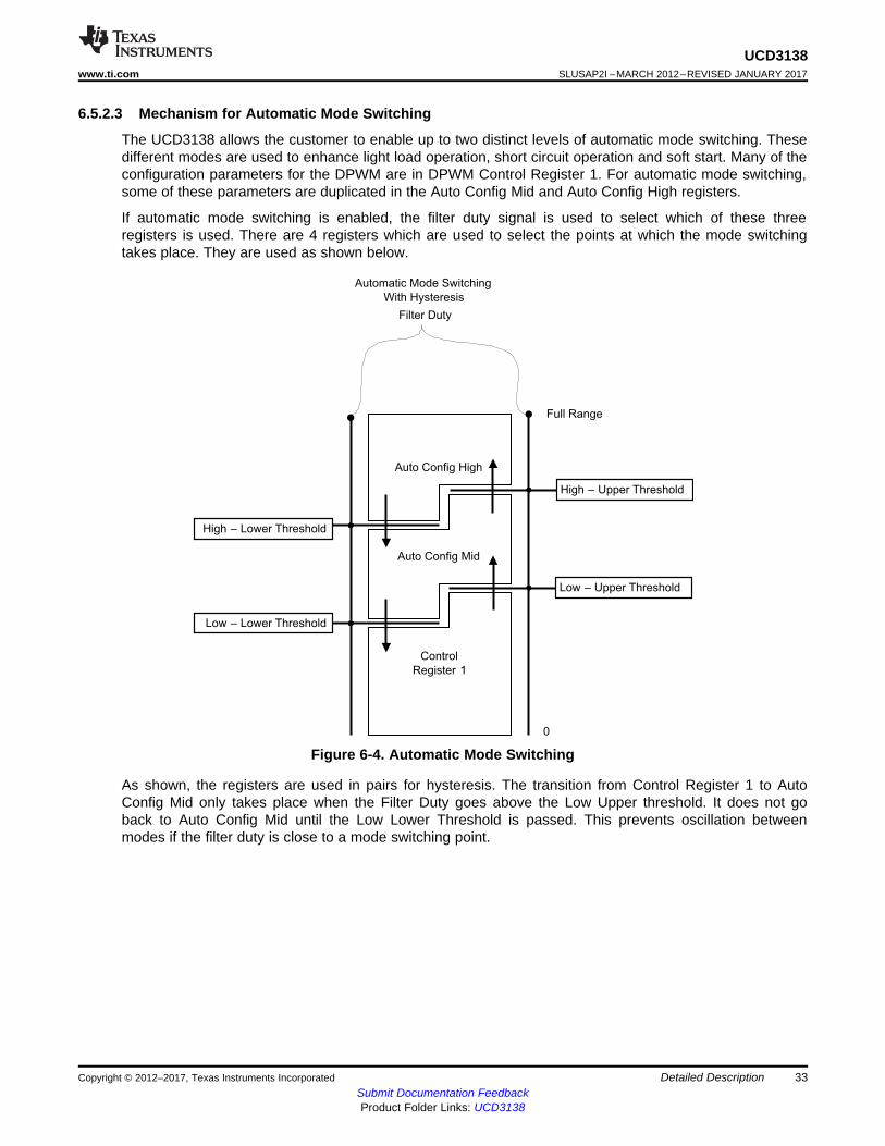
Filter Duty
Low – Lower Threshold
High – Lower Threshold
Control
Register 1
Auto Config High
Auto Config Mid
High – Upper Threshold
Low – Upper Threshold
0
Full Range
Automatic Mode Switching
With Hysteresis
33
UCD3138www.ti.com SLUSAP2I –MARCH 2012–REVISED JANUARY 2017
Submit Documentation FeedbackProduct Folder Links: UCD3138
Detailed DescriptionCopyright © 2012–2017, Texas Instruments Incorporated
6.5.2.3 Mechanism for Automatic Mode Switching
The UCD3138 allows the customer to enable up to two distinct levels of automatic mode switching. Thesedifferent modes are used to enhance light load operation, short circuit operation and soft start. Many of theconfiguration parameters for the DPWM are in DPWM Control Register 1. For automatic mode switching,some of these parameters are duplicated in the Auto Config Mid and Auto Config High registers.
If automatic mode switching is enabled, the filter duty signal is used to select which of these threeregisters is used. There are 4 registers which are used to select the points at which the mode switchingtakes place. They are used as shown below.
Figure 6-4. Automatic Mode Switching
As shown, the registers are used in pairs for hysteresis. The transition from Control Register 1 to AutoConfig Mid only takes place when the Filter Duty goes above the Low Upper threshold. It does not goback to Auto Config Mid until the Low Lower Threshold is passed. This prevents oscillation betweenmodes if the filter duty is close to a mode switching point.

A ON SELECT
A OFF SELECT
B ON SELECT
B OFF SELECT
EGEN A
EGEN B
EDGE GEN
PWM A
PWM B
B SELECT
A SELECT
INTRAMUX
A/B/C (N)A/B/C (N+1)
C (N+2)
C (N+3)
A(N)
B(N)
A(N+1)
B(N+1)
34
UCD3138SLUSAP2I –MARCH 2012–REVISED JANUARY 2017 www.ti.com
Submit Documentation FeedbackProduct Folder Links: UCD3138
Detailed Description Copyright © 2012–2017, Texas Instruments Incorporated
6.5.3 DPWMC, Edge Generation, IntraMuxThe UCD3138 has hardware for generating complex waveforms beyond the simple DPWMA and DPWMBwaveforms already discussed – DPWMC, the Edge Generation Module, and the IntraMux.
DPWMC is a signal inside the DPWM logic. It goes high at the Blanking A begin time, and low at theBlanking A end time.
The Edge Gen module takes DPWMA and DPWMB from its own DPWM module, and the next one, anduses them to generate edges for two outputs. For DPWM3, the DPWM0 is considered to be the nextDPWM. Each edge (rising and falling for DPWMA and DPWMB) has 8 options which can cause it.
The options are:0 = DPWM(n) A Rising edge1 = DPWM(n) A Falling edge2 = DPWM(n) B Rising edge3 = DPWM(n) B Falling edge4 = DPWM(n+1) A Rising edge5 = DPWM(n+1) A Falling edge6 = DPWM(n+1) B Rising edge7 = DPWM(n+1) B Falling edgeWhere “n" is the numerical index of the DPWM module of interest. For example n=1 refers to DPWM1.
The Edge Gen is controlled by the DPWMEDGEGEN register. It also has an enable/disable bit.
The IntraMux is controlled by the Auto Config registers. Intra Mux is short for intra multiplexer. TheIntraMux takes signals from multiple DPWMs and from the Edge Gen and combines them logically togenerate DPWMA and DPWMB signals This is useful for topologies like phase-shifted full bridge,especially when they are controlled with automatic mode switching. Of course, it can all be disabled, andDPWMA and DPWMB will be driven as described in the sections above. If the Intra Mux is enabled, highresolution must be disabled, and DPWM edge resolution goes down to 4 ns.
Here is a drawing of the Edge Gen/Intra Mux:
Figure 6-5. Edge Gen/Intra Mux
Here is a list of the IntraMux modes for DPWMA:
0 = DPWMA(n) pass through (default)1 = Edge-gen output, DPWMA(n)2 = DPWNC(n)3 = DPWMB(n) (Crossover)

35
UCD3138www.ti.com SLUSAP2I –MARCH 2012–REVISED JANUARY 2017
Submit Documentation FeedbackProduct Folder Links: UCD3138
Detailed DescriptionCopyright © 2012–2017, Texas Instruments Incorporated
4 = DPWMA(n+1)5 = DPWMB(n+1)6 = DPWMC(n+1)7 = DPWMC(n+2)8 = DPWMC(n+3)
and for DPWMB:0 = DPWMB(n) pass through (default)1 = Edge-gen output, DPWMB(n)2 = DPWNC(n)3 = DPWMA(n) (Crossover)4 = DPWMA(n+1)5 = DPWMB(n+1)6 = DPWMC(n+1)7 = DPWMC(n+2)8 = DPWMC(n+3)
The DPWM number wraps around just like the Edge Gen unit. For DPWM3 the following definitions apply:
DPWM(n) DPWM3DPWM(n+1) DPWM0DPWM(n+2) DPWM1DPWM(n+3) DPWM2
6.5.4 FilterThe UCD3138 filter is a PID filter with many enhancements for power supply control. Some of its featuresinclude:• Traditional PID Architecture• Programmable non-linear limits for automated modification of filter coefficients based on received
EADC error• Multiple coefficient sets fully configurable by firmware• Full 24-bit precision throughout filter calculations• Programmable clamps on integrator branch and filter output• Ability to load values into internal filter registers while system is running• Ability to stall calculations on any of the individual filter branches• Ability to turn off calculations on any of the individual filter branches• Duty cycle, resonant period, or phase shift generation based on filter output.• Flux balancing• Voltage feed forward

P26I
D
24
All are S0.23
+24
24
Saturate Yn
S2.23 S0.23
24Shifter
S0.23
24
Yn Scale
Clamp
S0.23
24
Filter YnClamp High
Filter YnClamp Low
Filter Yn
X
24
24
24
Kp Coef
Xn-1 Reg
Xn 1624
<>
9
9
16
242424
24
24
24
Clamp
Kd yn_reg
Kd alpha
9
16
9 24
24
24
24
P
I
D
Limit Comparator
PID Filter Branch Stages
Ki High
EADC_DATA
9
999
24
32
Ki Coef
Kd coef
Limit 5
9
9
Limit 6
…..
Limit 0Coefficient
select
Ki Low
OptionalSelected
by
KI_ADDER_MODE
Clamp
X
X
X
+
-
+
+
Ki_yn reg
Round
X Xn n-1–
36
UCD3138SLUSAP2I –MARCH 2012–REVISED JANUARY 2017 www.ti.com
Submit Documentation FeedbackProduct Folder Links: UCD3138
Detailed Description Copyright © 2012–2017, Texas Instruments Incorporated
Here is the first section of the Filter :
Figure 6-6. First Section of the Filter
The filter input, Xn, generally comes from a front end. Then there are three branches, P, I. and D. Notethat the D branch also has a pole, Kd Alpha. Clamps are provided both on the I branch and on the Dalpha pole.
The filter also supports a nonlinear mode, where up to 7 different sets of coefficients can be selecteddepending on the magnitude of the error input Xn. This can be used to increase the filter gain for highererrors to improve transient response.
Here is the output section of the filter (S0.23 means that there is 1 sign bit, 0 integer bits and 23 fractionalbits):
Figure 6-7. Output Section of the Filter

18
24
14
38 18
KCompx
DPWMx Period
Loop_VFF
Filter YN (Duty %) Filter Duty
S0.23
14.0
14.0
14.0
14.0
S14.23
Resonant Duty 14.0
Round to18 bits,
Clamp toPositive
Clamp
Filter OutputClamp High
Filter OutputClamp Low
X14.414.4
OUTPUT_MULT_SEL
14
Bits [17:4]
Filter Period
24
14
38 18
KCompx
DPWMx Period
Filter YN
S0.23
14.014.0
14.0
S14.23
Round to18 bits,
Clamp toPositive
Truncate
low 4 bitsX14.0
PERIOD_MULT_SEL
14.4
37
UCD3138www.ti.com SLUSAP2I –MARCH 2012–REVISED JANUARY 2017
Submit Documentation FeedbackProduct Folder Links: UCD3138
Detailed DescriptionCopyright © 2012–2017, Texas Instruments Incorporated
This section combines the P, I, and D sections, and provides for saturation, scaling, and clamping.
There is a final section for the filter, which permits its output to be matched to the DPWM:
Figure 6-8. Final Section for the Filter
This permits the filter output to be multiplied by a variety of correction factors to match the DPWM Period,to provide for Voltage Feed Forward, or for other purposes. After this, there is another clamp. For resonantmode, the filter can be used to generate both period and duty cycle.
Figure 6-9. Resonant Mode
6.5.4.1 Loop Multiplexer
The Loop Mux controls interconnections between the filters, front ends, and DPWMs. Any filter, front end,and DPWM can be combined with each other in many configurations.
It also controls the following connections:• DPWM to Front End• Front End DAC control from Filters or Constant Current/Constant Power Module• Filter Special Coefficients and Feed Forward• DPWM synchronization• Filter to DPWM
The following control modules are configured in the Loop Mux:• Constant Power/Constant Current

38
UCD3138SLUSAP2I –MARCH 2012–REVISED JANUARY 2017 www.ti.com
Submit Documentation FeedbackProduct Folder Links: UCD3138
Detailed Description Copyright © 2012–2017, Texas Instruments Incorporated
• Cycle Adjustment (Current and flux balancing)• Global Period• Light Load (Burst Mode)• Analog Peak Current Mode
6.5.4.2 Fault Multiplexer
In order to allow a flexible way of mapping several fault triggering sources to all the DPWMs channels, theUCD3138 provides an extensive array of multiplexers that are united under the name Fault Mux module.
The Fault Mux Module supports the following types of mapping between all the sources of fault and alldifferent fault response mechanism inside each DPWM module.• Many fault sources mapped to a single fault response mechanism. For instance an analog comparator
in charge of over voltage protection, a digital comparator in charge of over current protection and anexternal digital fault pin can be all mapped to a fault-A signal connected to a single FAULT MODULEand shut down DPWM1-A.
• A single fault source can be mapped to many fault response mechanisms inside many DPWMmodules. For instance an analog comparator in charge of over current protection can be mapped toDPWM-0 through DPWM-3 by way of several fault modules.
• Many fault sources can be mapped to many fault modules inside many DPWM modules.

FAULT - CBC
FAULT - AB
FAULT -A
DCOMP– 4X
EXT GPIO– 4X
ACOMP – 7X
FAULT -B
FAULT MODULE
FAULT MODULE
FAULT MODULE
CYCLE BY CYCLE
AB FLAG
AB FLAG
A FLAG
B FLAG
FAULT MUX
ALL_FAULT_EN DPWM_EN
DPWM
CBC_FAULT_EN
CBC_PWM_AB_EN
FAULT MODULE
ANALOG PCM
Bit20 in DPWMCTRL0
Bit30 in DPWMFLTCTRL
Bit 31 in DPWMFLTCTRL Bit0 in DPWMCTRL0
DISABLE PWM A AND B
DISABLE PWM A AND B
DISABLE PWM A ONLY
DISABLE PWM B ONLY
39
UCD3138www.ti.com SLUSAP2I –MARCH 2012–REVISED JANUARY 2017
Submit Documentation FeedbackProduct Folder Links: UCD3138
Detailed DescriptionCopyright © 2012–2017, Texas Instruments Incorporated
The Fault Mux Module provides a multitude of fault protection functions within the UCD3138 high-speedloop (front end control, filter, DPWM and loop Mux modules). The Fault Mux Module allows highlyconfigurable fault generation based on digital comparators, high-speed analog comparators and externalfault pins. Each of the fault inputs to the DPWM modules can be configured to one or any combination ofthe fault events provided in the Fault Mux Module.
Each one of the DPWM engines has four fault modules. The modules are called CBC fault module, ABfault module, A fault module and B fault module.
The internal circuitry in all the four fault modules is identical, and the difference between the modules islimited to the way the modules are attached to the DPWMs.

CYCLE BY CYCLECLIMFAULT - CBC
FAULT MODULE
FAULT IN FAULT FLAG
MA
X C
OU
NT
FA
ULT
EN
DP
WM
EN
40
UCD3138SLUSAP2I –MARCH 2012–REVISED JANUARY 2017 www.ti.com
Submit Documentation FeedbackProduct Folder Links: UCD3138
Detailed Description Copyright © 2012–2017, Texas Instruments Incorporated
Figure 6-10. Fault Module
All fault modules provide immediate fault detection but only once per DPWM switching cycle. Each one ofthe fault modules own a separate max_count and the fault flag will be set only if sequential cycle-by-cyclefaults count exceeds max_count.
Once the fault flag is set DPWMs need to be disabled by DPWM_EN going low in order to clear the faultflags.
NOTEAll four Fault Modules share the same DPWM_EN control, all fault flags (output of FaultModules) will be cleared simultaneously.
All four Fault Modules share the same global FAULT_EN as well. Therefore a specific Fault Modulecannot be enabled/ disabled separately.
Figure 6-11. Cycle by Cycle Block
Unlike fault modules, only one cycle by cycle block is available in each DPWM module.
The cycle by cycle block works in conjunction with CBC Fault Module and enables DPWM reaction tosignals arriving from analog peak current mode (PCM) module.
The fault Mux module supports the following basic functions:• 4 digital comparators with programmable thresholds and fault generation• Configuration for 7 high-speed analog comparators with programmable thresholds and fault generation• External GPIO detection control with programmable fault generation• Configurable DPWM fault generation for DPWM current limit fault, DPWM overvoltage detection fault,
DPWM A external fault, DPWM B external fault and DPWM IDE flag• Clock failure detection for high and low frequency oscillator blocks• Discontinuous conduction mode detection

Digital Comparator 0
Control
Digital Comparator 1Control
Digital Comparator 2Control
Digital Comparator 3
Control
Front End
Control 0
Front EndControl 1
Front EndControl 2
Analog
Comparator 0
Analog Comparator 0
Control
AnalogComparator 1
Analog Comparator 1Control
Analog
Comparator 2
Analog Comparator 2
Control
Analog
Comparator 3
Analog Comparator 3
Control
AnalogComparator 4
Analog Comparator 4Control
Analog
Comparator 5
Analog Comparator 5
Control
AnalogComparator 6
Analog Comparator 6Control
External GPIODetection
fault[2:0]
DPWM 0 DPWM 1 DPWM 2 DPWM 3
DPWM 0
Fault Control
DPWM 1
Fault Control
DPWM 2
Fault Control
DPWM 3
Fault Control
Analog ComparatorAutomated Ramp
DCM DetectionHFO/LFO
Fail Detect
41
UCD3138www.ti.com SLUSAP2I –MARCH 2012–REVISED JANUARY 2017
Submit Documentation FeedbackProduct Folder Links: UCD3138
Detailed DescriptionCopyright © 2012–2017, Texas Instruments Incorporated
Figure 6-12. Fault Mux Block Diagram
6.5.5 Communication Ports
6.5.5.1 SCI (UART) Serial Communication Interface
A maximum of two independent Serial Communication Interface (SCI) or Universal AsynchronousReceiver/Transmitter pre-scaler (UART) interfaces are included within the device for asynchronous start-stop serial data communication (see the pin out sections for details) Each interface has a 24 bit forsupporting programmable baud rates and has programmable data word and stop bit options. Half or fullduplex operation is configurable through register bits. A loop back feature can also be setup for firmwareverification. Both SCI-TX and SCI-RX pin sets can be used as GPIO pins when the peripheral is not beingused.
6.5.5.2 PMBUS
The PMBus Interface supports independent master and slave modes controlled directly by firmwarethrough a processor bus interface. Individual control and status registers enable firmware to send orreceive I2C, SMBus or PMBus messages in any of the accepted protocols, in accordance with the I2CSpecification, SMBus Specification (Version 2.0) and the PMBUS Power System Management ProtocolSpecification.
The PMBus interface is controlled through a processor bus interface, utilizing a 32-bit data bus and 6-bitaddress bus. The PMBus interface is connected to the expansion bus, which features 4 byte writeenables, a peripheral select dedicated for the PMBus interface, separated 32-bit data buses for readingand writing of data and active-low write and output enable control signals. In addition, the PMBus Interfaceconnects directly to the I2C/SMBus/PMBus Clock, Data, Alert, and Control signals.
Example: PMBus Address Decode via ADC12 Reading
The user can allocate 2 pins of the 12-bit ADC input channels, AD_00 and AD_01, for PMBus addressdecoding. At power-up the device applies IBIAS to each address detect pin and the voltage on that pin iscaptured by the internal 12-bit ADC.
Where bin(VAD0x) is the address bin for one of 12 address as shown in Figure 6-13.

Vdd
IBIAS
To ADC Mux
On/Off Control
AD00,
AD01pin
Resistor toset PMBus
Address
42
UCD3138SLUSAP2I –MARCH 2012–REVISED JANUARY 2017 www.ti.com
Submit Documentation FeedbackProduct Folder Links: UCD3138
Detailed Description Copyright © 2012–2017, Texas Instruments Incorporated
Figure 6-13. PMBus Address Detection Method
6.5.5.3 General Purpose ADC12
The ADC12 is a 12 bit, high speed analog to digital converter, equipped with the following options:
• Typical conversion speed of 267 ksps• Conversions can consist from 1 to 16 ADC channel conversions in any desired sequence• Post conversion averaging capability, ranging from 4X, 8X, 16X or 32X samples• Configurable triggering for ADC conversions from the following sources: firmware, DPWM rising edge,
ADC_EXT_TRIG pin or Analog Comparator results• Interrupt capability to embedded processor at completion of ADC conversion• Six digital comparators on the first 6 channels of the conversion sequence using either raw ADC data
or averaged ADC data• Two 10 µA current sources for excitation of PMBus addressing resistors• Dual sample and hold for accurate power measurement• Internal temperature sensor for temperature protection and monitoring
The control module ADC12 Contol Block Diagram contains the control and conversion logic for auto-sequencing a series of conversions. The sequencing is fully configurable for any combination of 16possible ADC channels through an analog multiplexer embedded in the ADC12 block. Once converted,the selected channel value is stored in the result register associated with the sequence number. Inputchannels can be sampled in any desired order or programmed to repeat conversions on the same channelmultiple times during a conversion sequence. Selected channel conversions are also stored in the resultregisters in order of conversion, where the result 0 register is the first conversion of a 16-channelsequence and result 15 register is the last conversion of a 16-channel sequence. The number of channelsconverted in a sequence can vary from 1 to 16.
Unlike EADC0 through EADC2, which are primarily designed for closing high speed compensation loops,the ADC12 is not usually used for loop compensation purposes. The EADC converters have asubstantially faster conversion rate, thus making them more attractive for closed loop control. The ADC12features make it best suited for monitoring and detection of currents, voltages, temperatures and faults.Please see the Typical Characteristics plots for the temperature variation associated with this function.

ADC
Channels
S/H12-bit SAR
ADC
12-bit SAR
ADC
ADC12 Block
ADC12
Control
ADC Channel
ADC
Averaging
Digital
Comparators
DPWM
Modules
ADC12 Registers
Analog
Comparators
ADC External Trigger (from pin)
43
UCD3138www.ti.com SLUSAP2I –MARCH 2012–REVISED JANUARY 2017
Submit Documentation FeedbackProduct Folder Links: UCD3138
Detailed DescriptionCopyright © 2012–2017, Texas Instruments Incorporated
Figure 6-14. ADC12 Control Block Diagram
6.5.5.4 Timers
External to the Digital Power Peripherals there are 3 different types of timers in UCD3138. They are the24-bit timer, 16-bit timer and the Watchdog timer
6.5.5.4.1 24-bit PWM Timer
There is one 24 bit counter PWM timer which runs off the Interface Clock and can further be divided downby an 8-bit pre-scalar to generate a slower PWM time period. The timer has two compare registers (DataRegisters) for generating the PWM set/unset events. Additionally, the timer has a shadow register (DataBuffer register) which can be used to store CPU updates of the compare events while still using the timer.The selected shadow register update mode happens after the compare event matches.
The two capture pins TCMP0 and TCMP1 are inputs for recording a capture event. A capture event canbe set either to rising, falling, or both edges of the capture pin. Upon this event, the counter value is storedin the corresponding capture data register.
The counter reset can be configured to happen on a counter roll over, a compare equal event, or bysoftware controlled register. Five Interrupts from the PWM timer can be set, which are the counter rolloverevent (overflow), either capture event 0 or 1, or the two comparison match events. Each interrupt can bedisabled or enabled.
Upon an event comparison on only the second event, the TCMP pin can be configured to set, clear, toggleor have no action at the output. The value of PWM pin output can be read for status or simply configuredas general purpose I/O for reading the value of the input at the pin. The first compare event can only beused as an interrupt.
44
UCD3138SLUSAP2I –MARCH 2012–REVISED JANUARY 2017 www.ti.com
Submit Documentation FeedbackProduct Folder Links: UCD3138
Detailed Description Copyright © 2012–2017, Texas Instruments Incorporated
6.5.5.4.2 16-Bit PWM Timers
There are four 16 bit counter PWM timers which run off the Interface Clock and can further be divideddown by a 8-bit pre-scaler to generate slower PWM time periods. Each timer has two compare registers(Data Registers) for generating the PWM set/unset events. Additionally, each timer has a shadow register(Data Buffer register) which can be used to store CPU updates of compare events while still using thetimer. The selected shadow register update mode happens after the compare event matches.
The counter reset can be configured to happen on a counter roll over, a compare equal event, or by asoftware controlled register. Interrupts from the PWM timer can be set due to the counter rollover event(overflow) or by the two comparison match events. Each comparison match and the overflow interruptscan be disabled or enabled.
Upon an event comparison, the PWM pin can be configured to set, clear, toggle or have no action at theoutput. The value of PWM pin output can be read for status or simply configured as General Purpose I/Ofor reading the value of the input at the pin.
6.5.5.4.3 Watchdog Timer
A watchdog timer is provided on the device for ensuring proper firmware loop execution. The timer isclocked off of a separate low speed oscillator source. If the timer is allowed to expire, a reset condition isissued to the ARM processor. The watchdog is reset by a simple CPU write bit to the watchdog keyregister by the firmware routine. On device power-up the watchdog is disabled. Yet after it is enabled, thewatchdog cannot be disabled by firmware. Only a device reset can put this bit back to the default disabledstate. A half timer flag is also provided for status monitoring of the watchdog.
6.5.6 Miscellaneous AnalogThe Miscellaneous Analog Control (MAC) Registers are a catch-all of registers that control and monitor awide variety of functions. These functions include device supervisory features such as Brown-Out andpower saving configuration, general purpose input/output configuration and interfacing, internaltemperature sensor control and current sharing control.
The MAC module also provides trim signals to the oscillator and AFE blocks. These controls are usuallyused at the time of trimming at manufacturing; therefore this document will not cover these trim controls.
The MAC registers and peripherals are all available in the UCD3138 (64 pin version). Other UCD3138devices may have reduced resources. See the device pin out description for details.
6.5.7 Package ID InformationPackage ID register includes information regarding the package type of the device and can be read byfirmware for reporting through PMBus or for other package sensitive decisions.
BIT NUMBER 1:0Bit Name PKG_IDAccess R/W
Default 0 – UCD3138RGC,1 – UCD3138RHA
6.5.8 BrownoutBrownout function is used to determine if the device supply voltage is lower than a threshold voltage, acondition that may be considered unsafe for proper operation of the device.
The brownout threshold is higher than the reset threshold voltage; therefore, when the supply voltage islower than brownout threshold, it still does not necessarily trigger a device reset.

45
UCD3138www.ti.com SLUSAP2I –MARCH 2012–REVISED JANUARY 2017
Submit Documentation FeedbackProduct Folder Links: UCD3138
Detailed DescriptionCopyright © 2012–2017, Texas Instruments Incorporated
The brownout interrupt flag can be polled or alternatively can trigger an interrupt to service such case byan interrupt service routine. Please see the Power On Reset (POR) / Brown Out Reset (BOR) section.
6.5.9 Global I/OUp to 30 pins in UCD3138 can be configured to serve as a general purpose input or output pin (GPIO).This includes all digital input or output pins except for the RESET pin.
The pins that cannot be configured as GPIO pins are the supply pins, ground pins, ADC-12 analog inputpins, EADC analog input pins and the RESET pin.
There are two ways to configure and use the digital pins as GPIO pins:1. Through the centralized Global I/O control registers.2. Through the distributed control registers in the specific peripheral that shares it pins with the standard
GPIO functionality.
The Global I/O registers offer full control of:
1. Configuring each pin as a GPIO.2. Setting each pin as input or output.3. Reading the pin’s logic state, if it is configured as an input pin.4. Setting the logic state of the pin, if it is configured as an output pin.5. Configuring pin/pins as open drain or push-pull (Normal)
The Global I/O registers include Global I/O EN register, Global I/O OE Register, Global I/O Open DrainControl Register, Global I/O Value Register and Global I/O Read Register.
The following is showing the format of Global I/O EN Register (GLBIOEN) as an example:
BIT NUMBER 29:0Bit Name GLOBAL_IO_ENAccess R/WDefault 00_0000_0000_0000_0000_0000_0000_0000
Bits 29-0: GLOBAL_IO_EN – This register enables the global control of digital I/O pins0 = Control of IO is done by the functional block assigned to the IO (Default)1 = Control of IO is done by Global IO registers.
BIT PIN_NAMEPIN NUMBER
UCD3138-64 PIN UCD3138-40 PIN29 FAULT[3] 43 NA28 ADC_EXT_TRIG 12, 26 827 TCK 37 2126 TDO 38 2025 TMS 40 2424 TDI 39 2323 SCI_TX[1] 29 NA22 SCI_TX[0] 14 2221 SCI_RX[1] 30 NA20 SCI_RX[0] 13 2319 TMR_CAP 12, 26, 41 8, 2118 TMR_PWM[1] 32 NA17 TMR_PWM[0] 12, 26, 31, 37 2116 PMBUS-CLK 15 915 PMBUS-DATA 16 10

TemperatureSensor
Ch14
ADC 12
Temp Cal
46
UCD3138SLUSAP2I –MARCH 2012–REVISED JANUARY 2017 www.ti.com
Submit Documentation FeedbackProduct Folder Links: UCD3138
Detailed Description Copyright © 2012–2017, Texas Instruments Incorporated
BIT PIN_NAMEPIN NUMBER
UCD3138-64 PIN UCD3138-40 PIN14 CONTROL 30 2013 ALERT 29 1912 EXT_INT 26, 34 NA11 FAULT[2] 42 2510 FAULT[1] 36 239 FAULT[0] 35, 39 228 SYNC 12, 26,37 8, 217 DPWM3B 24 186 DPWM3A 23 175 DPWM2B 22 164 DPWM2A 21 153 DPWM1B 20 142 DPWM1A 19 131 DPWM0B 18 120 DPWM0A 17 11
6.5.10 Temperature Sensor ControlTemperature sensor control register provides internal temperature sensor enabling and trimmingcapabilities. The internal temperature sensor is disabled as default.
Figure 6-15. Internal Temp Sensor
Temperature sensor is calibrated at room temperature (25 °C) via a calibration register value.
The temperature sensor is measured using ADC12 (via Ch14). The temperature is then calculated using amathematical formula involving the calibration register (this effectively adds a delta to the ADCmeasurement).
The temperature sensor can be enabled or disabled.
6.5.11 I/O Mux ControlIn different packages of UCD3138 several I/O functions are multiplexed and routed toward a singlephysical pin. I/O Mux Control register may be used in order to choose a single specific functionality that isdesired to be assigned to a physical device pin for your application.
6.5.12 Current Sharing ControlUCD3138 provides three separate modes of current sharing operation.
• Analog bus current sharing

EXT CAP
AD02400 Ω
Digital
RSHARE
250 Ω
3.3 V
ISHARE
ADC12 andCMP
ESD
ESD
250 Ω3.2 kΩ
ESD
AD13
3.3V
SW2
SW1
SW3
3.3 V
ADC12 andCMP
47
UCD3138www.ti.com SLUSAP2I –MARCH 2012–REVISED JANUARY 2017
Submit Documentation FeedbackProduct Folder Links: UCD3138
Detailed DescriptionCopyright © 2012–2017, Texas Instruments Incorporated
• PWM bus current sharing• Master/Slave current sharing• AD02 has a special ESD protection mechanism that prevents the pin from pulling down the current-
share bus if power is missing from the UCD3138
The simplified current sharing circuitry is shown in the drawing below:
Figure 6-16. Simplified Current Sharing CircuitryCURRENT SHARING MODE FOR TEST ONLY,
ALWAYS KEEP 00 CS_MODE EN_SW1 EN_SW2 DPWM
Off or Slave Mode (3-state) 00 00 (default) 0 0 0PWM Bus 00 01 1 0 ACTIVEOff or Slave Mode (3-state) 00 10 0 0 0Analog Bus or Master 00 11 0 1 0
The period and the duty of 8-bit PWM current source and the state of the SW1 and SW2 switches can becontrolled through the current sharing control register (CSCTRL).
6.5.13 Temperature ReferenceThe temperature reference register (TEMPREF) provides the ADC12 count when ADC12 measures theinternal temperature sensor (channel 14) during the factory trim and calibration.
This information can be used by different periodic temperature compensation routines implemented in thefirmware. But it should not be overwritten by firmware, otherwise this factory written value will be lost.

48
UCD3138SLUSAP2I –MARCH 2012–REVISED JANUARY 2017 www.ti.com
Submit Documentation FeedbackProduct Folder Links: UCD3138
Detailed Description Copyright © 2012–2017, Texas Instruments Incorporated
6.6 Device Functional ModesThe DPWM is a complex logic system which is highly configurable to support several different powersupply topologies. The discussion below will focus primarily on waveforms, timing and register settings,rather than on logic design.
The DPWM is centered on a period counter, which counts up from 0 to PRD, and then is reset and startsover again.
The DPWM logic causes transitions in many digital signals when the period counter hits the target valuefor that signal.
6.6.1 Normal ModeIn Normal mode, the Filter output determines the pulse width on DPWM A. DPWM B fits into the rest ofthe switching period, with a dead time separating it from the DPWM A on-time. It is useful for bucktopologies, among others. Here is a drawing of the Normal Mode waveforms:

Start of Period
Period Counter
Start of Period
Period
DPWM Output A
Cycle Adjust A (High Resolution)
Filter Duty (High Resolution)
Event 1
Event 3 – Event 2 (High Res)
Event 4 (High Res)
DPWM Output B
Blanking B Begin
Blanking B End
Phase Trigger
Sample Trigger 2
To Other
Modules
Normal Mode Closed Loop
Events which change with DPWM mode:
DPWM A Rising Edge = Event 1
DPWM A Falling Edge = Event 1 + Filter Duty + Cycle Adjust A
Adaptive Sample Trigger A = Event 1 + Filter Duty + Adaptive Sample Register or
Adaptive Sample Trigger B = Event 1 + Filter Duty/2 + Adaptive Sample Register
DPWM B Rising Edge = Event 1 + Filter Duty + Cycle Adjust A + (Event 3 – Event 2)
DPWM B Falling Edge = Event 4
Phase Trigger = Phase Trigger Register value or Filter Duty
Events always set by their registers, regardless of mode:
Sample Trigger 1, Sample Trigger 2, Blanking A Begin, Blanking A End, Blanking B
Begin, Blanking B End
Filter controlled edge
Sample Trigger 1
Blanking A Begin
Blanking A EndTo Other
Modules
Adaptive Sample Trigger A
Adaptive Sample Trigger B
49
UCD3138www.ti.com SLUSAP2I –MARCH 2012–REVISED JANUARY 2017
Submit Documentation FeedbackProduct Folder Links: UCD3138
Detailed DescriptionCopyright © 2012–2017, Texas Instruments Incorporated
Figure 6-17. Normal Mode Closed Loop
Cycle adjust A can be used to adjust pulse widths on individual phases of a multi-phase system. This canbe used for functions like current balancing. The Adaptive Sample Triggers can be used to sample in themiddle of the on-time (for an average output), or at the end of the on-time (to minimize phase delay) TheAdaptive Sample Register provides an offset from the center of the on-time. This can compensate forexternal delays, such as MOSFET and gate driver turn on times.

Phase Shift
Phase Trigger = Phase Trigger Register value or Filter Duty
DPWM0 Start of Period
Period Counter
DPWM0 Start of Period
DPWM1 Start of Period
Period Counter
DPWM1 Start of Period
50
UCD3138SLUSAP2I –MARCH 2012–REVISED JANUARY 2017 www.ti.com
Submit Documentation FeedbackProduct Folder Links: UCD3138
Detailed Description Copyright © 2012–2017, Texas Instruments Incorporated
Blanking A-Begin and Blanking A-End can be used to blank out noise from the MOSFET turn on at thebeginning of the period (DPWMA rising edge). Blanking B could be used at the turn off time of DPWMB.The other edges are dynamic, so blanking is more difficult.
Cycle Adjust B has no effect in Normal Mode.
6.6.2 Phase ShiftingIn most modes, it is possible to synchronize multiple DPWM modules using the phase shift signal. Thephase shift signal has two possible sources. It can come from the Phase Shift register. This provides afixed value, which is useful for an interleaved PFC, for example.
The phase shift value can also come from the filter output. In this case, the changes in the filter outputcauses changes in the phase relationship of two DPWM modules. This is useful for phase shifted fullbridge topologies.
The following figure shows the mechanism of phase shift:
Figure 6-18. Phase Shift

Adaptive Sample Trigger B
Start of Period
Period Counter
Start of Period
Period
Adaptive Sample Trigger A
DPWM Output A
Cycle Adjust A (High Resolution)
Filter Duty (High Resolution)
Event 1
To Other
Modules
Multi Mode Closed Loop
Events which change with DPWM mode:
DPWM A Rising Edge = Event 1
DPWM A Falling Edge = Event 1 + Filter Duty + Cycle Adjust A
Adaptive Sample Trigger A = Event 1 + Filter Duty + Adaptive Sample Register or
Adaptive Sample Trigger B = Event 1 + Filter Duty/2 + Adaptive Sample Register
DPWM B Rising Edge = Event 3
DPWM B Falling Edge = Event 3 + Filter Duty + Cycle Adjust B
Phase Trigger = Phase Trigger Register value or Filter Duty
Events always set by their registers, regardless of mode:
Sample Trigger 1, Sample Trigger 2, Blanking A Begin, Blanking A End, Blanking B
Begin, Blanking B End
Filter controlled edge
Event 3 (High Resolution)
Cycle Adjust B (High Resolution)
Filter Duty (High Resolution)
DPWM Output B
Blanking B Begin
Blanking B End
Phase Trigger
Sample Trigger 2
To Other
Modules
Sample Trigger 1
Blanking A Begin
Blanking A End
51
UCD3138www.ti.com SLUSAP2I –MARCH 2012–REVISED JANUARY 2017
Submit Documentation FeedbackProduct Folder Links: UCD3138
Detailed DescriptionCopyright © 2012–2017, Texas Instruments Incorporated
6.6.3 DPWM Multiple Output ModeMulti mode is used for systems where each phase has only one driver signal. It enables each DPWMperipheral to drive two phases with the same pulse width, but with a time offset between the phases, andwith different cycle adjusts for each phase.
Here is a diagram for Multi-Mode:
Figure 6-19. Multi Mode Closed Loop
Event 2 and Event 4 are not relevant in Multi mode.

Start of Period
Period Counter
Start of Period
Filter Period
Adaptive Sample Trigger A
Sample Trigger 1
DPWM Output A
Filter Duty – Average Dead Time
Event 1
Event 3 - Event 2
Period Register – Event 4
DPWM Output B
Blanking A Begin
Blanking A End
Blanking B Begin
Blanking B End
Phase Trigger
Sample Trigger 2
To Other
Modules
To Other
Modules
Resonant Symmetrical Closed Loop
Events which change with DPWM mode:
Dead Time 1 = Event 3 – Event 2
Dead Time 2 = Event 1 + Period Register – Event 4)
Average Dead Time = (Dead Time 1 + Dead Time 2)/2
DPWM A Rising Edge = Event 1
DPWM A Falling Edge = Event 1 + Filter Duty – Average Dead Time
Adaptive Sample Trigger A = Event 1 + Filter Duty + Adaptive Sample Register
Adaptive Sample Trigger B = Event 1 + Filter Duty/2 + Adaptive Sample Register
DPWM B Rising Edge = Event 1 + Filter Duty – Average Dead Time + (Event 3 – Event 2)
DPWM B Falling Edge = Filter Period – (Period Register – Event 4)
Phase Trigger = Phase Trigger Register value or Filter Duty
Events always set by their registers, regardless of mode:
Sample Trigger 1, Sample Trigger 2, Blanking A Begin, Blanking A End, Blanking B Begin,
Blanking B End
Filter controlled edge
Adaptive Sample Trigger B
52
UCD3138SLUSAP2I –MARCH 2012–REVISED JANUARY 2017 www.ti.com
Submit Documentation FeedbackProduct Folder Links: UCD3138
Detailed Description Copyright © 2012–2017, Texas Instruments Incorporated
DPWMB can cross over the period boundary safely, and still have the proper pulse width, so full 100%pulse width operation is possible. DPWMA cannot cross over the period boundary.
Since the rising edge on DPWM B is also fixed, Blanking B-Begin and Blanking B-End can be used forblanking this rising edge.
And, of course, Cycle Adjust B is usable on DPWM B.
6.6.4 DPWM Resonant ModeThis mode provides a symmetrical waveform where DPWMA and DPWMB have the same pulse width. Asthe switching frequency changes, the dead times between the pulses remain the same.
The equations for this mode are designed for a smooth transition from PWM mode to resonant mode, asdescribed in Section 6.5.2.2. Here is a diagram of this mode:
Figure 6-20. Resonant Symmetrical Closed Loop

Start of Period
Period Counter
Start of Period
Period
Sample Trigger 1
DPWM Output A
Filter Duty/2 (High Resolution)
Period/2
DPWM Output B
Blanking A Begin
Blanking A End
Blanking B Begin
Blanking B End
Phase Trigger
Sample Trigger 2
To Other
Modules
To Other
Modules
Triangular Mode Closed Loop
Events which change with DPWM mode:
DPWM A Rising Edge = None
DPWM A Falling Edge = None
Adaptive Sample Trigger = None
DPWM B Rising Edge = Period/2 - Filter Duty/2 + Cycle Adjust A
DPWM B Falling Edge = Period/2 + Filter Duty/2 + Cycle Adjust B
Phase Trigger = Phase Trigger Register value or Filter Duty
Events always set by their registers, regardless of mode:
Sample Trigger 1, Sample Trigger 2, Blanking A Begin, Blanking A End, Blanking B
Begin, Blanking B End
Filter controlled edge
Cycle Adjust A (High Resolution)
Cycle Adjust B (High Resolution)
53
UCD3138www.ti.com SLUSAP2I –MARCH 2012–REVISED JANUARY 2017
Submit Documentation FeedbackProduct Folder Links: UCD3138
Detailed DescriptionCopyright © 2012–2017, Texas Instruments Incorporated
The Filter has two outputs, Filter Duty and Filter Period. In this case, the Filter is configured so that theFilter Period is twice the Filter Duty. So if there were no dead times, each DPWM pin would be on for halfof the period. For dead time handling, the average of the two dead times is subtracted from the Filter Dutyfor both DPWM pins. Therefore, both pins will have the same on-time, and the dead times will be fixedregardless of the period. The only edge which is fixed relative to the start of the period is the rising edge ofDPWM A. This is the only edge for which the blanking signals can be used easily.
6.6.5 Triangular ModeTriangular mode provides a stable phase shift in interleaved PFC and similar topologies. In this case, thePWM pulse is centered in the middle of the period, rather than starting at one end or the other. InTriangular Mode, only DPWM-B is available. Here is a diagram for Triangular Mode:
Figure 6-21. Triangular Mode Closed Loop
All edges are dynamic in triangular mode, so fixed blanking is not that useful. The adaptive sample triggeris not needed. It is very easy to put a fixed sample trigger exactly in the center of the FET on-time,because the center of the on-time does not move in this mode.

Start of Period
Period Counter
Start of Period
Period
Adaptive Sample Trigger B
Sample Trigger 1
DPWM Output A
Cycle Adjust A (High Resolution)
Filter Duty (High Resolution)
Event 1
Event 2 - Event 3 (High Resolution)
Event 4 (High Resolution)
DPWM Output B
Blanking A Begin
Blanking A End
Blanking B Begin
Blanking B End
Phase Trigger
Sample Trigger 2
To Other
Modules
To Other
Modules
Leading Edge Closed Loop
Events which change with DPWM mode:
DPWM A Falling Edge = Event 1
DPWM A Rising Edge = Event 1 - Filter Duty + Cycle Adjust A
Adaptive Sample Trigger A = Event 1 - Filter Duty + Adaptive Sample Register or
Adaptive Sample Trigger B = Event 1 - Filter Duty/2 + Adaptive Sample Register
DPWM B Rising Edge = Event 4
DPWM B Falling Edge = Event 1 - Filter Duty + Cycle Adjust A -(Event 2 – Event 3)
Phase Trigger = Phase Trigger Register value or Filter Duty
Events always set by their registers, regardless of mode:
Sample Trigger 1, Sample Trigger 2, Blanking A Begin, Blanking A End, Blanking B
Begin, Blanking B End
Adaptive Sample Trigger A
54
UCD3138SLUSAP2I –MARCH 2012–REVISED JANUARY 2017 www.ti.com
Submit Documentation FeedbackProduct Folder Links: UCD3138
Detailed Description Copyright © 2012–2017, Texas Instruments Incorporated
6.6.6 Leading Edge ModeLeading edge mode is very similar to Normal mode, reversed in time. The DPWM A falling edge is fixed,and the rising edge moves to the left, or backwards in time, as the filter output increases. The DPWM Bfalling edge stays ahead of the DPWMA rising edge by a fixed dead time. Here is a diagram of theLeading Edge Mode:
Figure 6-22. Leading Edge Closed Loop
As in the Normal mode, the two edges in the middle of the period are dynamic, so the fixed blankingintervals are mainly useful for the edges at the beginning and end of the period.

55
UCD3138www.ti.com SLUSAP2I –MARCH 2012–REVISED JANUARY 2017
Submit Documentation FeedbackProduct Folder Links: UCD3138
Application and ImplementationCopyright © 2012–2017, Texas Instruments Incorporated
7 Application and Implementation
NOTEInformation in the following applications sections is not part of the TI componentspecification, and TI does not warrant its accuracy or completeness. TI’s customers areresponsible for determining suitability of components for their purposes. Customers shouldvalidate and test their design implementation to confirm system functionality.
7.1 Application InformationThe UCD3138x has an extensive set of fully-programmable, high-performance peripherals that make itsuitable for a wide range of power supply applications. In order to make the part easier to use, TI hasprepared an extensive set of materials to demonstrate the features of the device for several keyapplications. In each case the following items are available:1. Full featured EVM hardware that demonstrates classic power supply functionality.2. An EVM user guide that contains schematics, bill-of-materials, layout guidance and test data
showcasing the performance and features of the device and the hardware.3. A firmware programmers manual that provides a step-by-step walk through of the code.
Table 7-1. Application Information
APPLICATION EVM DESCRIPTION
Phase shifted fullbridge
This EVM demonstrates a PSFB DC-DC power converter with digital control using the UCD3138x device. Control isimplemented by using PCMC with slope compensation. This simplifies the hardware design by eliminating the needfor a series blocking capacitors and providing the inherent input voltage feed-forward that comes from PCMC. Thecontroller is located on a daughter card and requires firmware in order to operate. This firmware, along with the entiresource code, is made available through TI. A free, custom function GUI is available to help the user experiment withthe different hardware and software enabled features. The EVM accepts a DC input from 350 VDC to 400 VDC, andoutputs a nominal 12 VDC with full load output power of 360 W, or full output current of 30 A.
LLC resonantconverter
This EVM demonstrates an LLC resonant half-bridge DC-DC power converter with digital control using theUCD3138x device. The controller is located on a daughter card and requires firmware in order to operate. Thisfirmware, along with the entire source code, is made available through TI. A free, custom function GUI is available tohelp the user experiment with the different hardware and software enabled features. The EVM accepts a DC inputfrom 350 VDC to 400 VDC, and outputs a nominal 12 VDC with full load output power of 340 W, or full output currentof 29 A.

QT1
QB1
Lr
ISOLATEDGATE Transformer SYNCHRONOUS
GATE DRIVE
PRIM
CURRENT
VOUT
+12V
T1
T1
ORING
CTL
VA
VBUS
QT2
QB2
D1
D2
T2
L1
Q5
RLC1
C2
R2
Q6
Q7
I_SHARE
Vout
Iout
I_pri
temp
Vin
VA
UCD3138
ARM7
FAULT0AD01
AD02/CMP0
AD03/CMP1/CMP2
AD04/CMP3
AD05/CMP4
AD00
AD06/CMP5
FAULT1
FAULT2
GPIO2
GPIO3
GPIO1
AD07/CMP6
AD08
AD09
DPWM0B
DPWM1B
DPWM2A
DPWM2B
ORING_CRTL
P_GOOD
DPWM3A
DPWM3B
Vout
ON/OFF
FAILURE
ACFAIL_OUT
ACFAIL_IN
I_pri
Iout
EADC0
EADC1
CLA0
CLA1
EADC2
DPWM0
DPWM1
DPWM2
DPWM3
Duty for mode
switching
Vref
Load Current
PCM
CBC
<
DP
WM
3A
DP
WM
3B
DP
WM
2A
DP
WM
2B
DP
WM
0B
DP
WM
1B
CPCC
PMBus
UART1UART0
PrimaryOSC
WD
RST
Memory
FAULT
CurrentSensing
I_pri
56
UCD3138SLUSAP2I –MARCH 2012–REVISED JANUARY 2017 www.ti.com
Submit Documentation FeedbackProduct Folder Links: UCD3138
Application and Implementation Copyright © 2012–2017, Texas Instruments Incorporated
7.2 Typical ApplicationThis section summarizes the PSFB EVM DC-DC power converter.
Figure 7-1. Phase-Shifted Full-Bridge
57
UCD3138www.ti.com SLUSAP2I –MARCH 2012–REVISED JANUARY 2017
Submit Documentation FeedbackProduct Folder Links: UCD3138
Application and ImplementationCopyright © 2012–2017, Texas Instruments Incorporated
7.2.1 Design Requirements
Table 7-2. Input Characteristics
PARAMETER CONDITIONS MIN TYP MAX UNITALL SPECIFICATIONS at Vin=400V and 25°C AMBIENT UNLESS OTHERWISE NOTED.Vin Input voltage range Normal Operating 350 385 420 VVinmax Max input voltage Continuous 420 VIin Input current Vin=350V, Full Load 1.15 AIstby Input no load current Output current is 0A 30 mAVon Under voltage lockout
Vin Decreasing (input voltage is detected on secondary side) 340 VVhys Vin Increasing 360 V
(1) Ripple and noise are measured with 10µF Tantalum capacitor and 0.1µF ceramic capacitor across output.
Table 7-3. Output Characteristics
PARAMETER CONDITIONS MIN TYP MAX UNITALL SPECIFICATIONS at Vin=400V and 25°C AMBIENT UNLESS OTHERWISE NOTED.VO Output voltage setpoint No load on outputs 12 VRegline Line regulation All outputs; 360 ≤ Vin ≤ 420; IO = IOmax 0.5 %Regload Load regulation All outputs; 0 ≤ IO ≤ IOmax; Vin = 400 V 1 %Vn Ripple and noise (1) 5Hz to 20 MHz 100 mVppIO Output current 0 30 Aη Efficiency at phase-shift mode Vo = 12 V, Io = 15 A 93%η Efficiency at PWM ZVS mode Vo = 12 V, Io = 15 A 93%η Efficiency at hard switching mode Vo = 12 V, Io = 15 A 90%Vadj Output adjust range 11.4 12.6 V
VtrTransient responseovershoot/undershoot 50% Load Step at 1AµS, min load at 2A ±0.36 V
tsettling Transient response settling time 100 µStstart Output rise time 10% to 90% of Vout 50 mS
Overshoot At Startup 2 %fs Switching frequency Over Vin and IO ranges 150 kHzIshare Current sharing accuracy 50% - full load ±5 %φ Loop phase margin 10% - Full load 45 degreeG Loop gain margin 10% - Full load 10 dB
7.2.2 Detailed Design Procedure
7.2.2.1 PCMC (Peak Current Mode Control) PSFB (Phase Shifted Full Bridge) Hardware ConfigurationOverview
The hardware configuration of the UCD3138x PCMC PSFB converter contains two critical elements thatare highlighted in the subsequent sections.• DPWM initialization - This section will highlight the key register settings and considerations necessary
for the UCD3138x to generate the correct MOSFET waveforms for this topology. This maintains theproper phase relationship between the MOSFETs and synchronous rectifiers as well as the proper setup required to function correctly with PCMC.
• PCMC initialization - This section will discuss the register settings and hardware considerationsnecessary to modulate the DPWM pins with PCMC and internal slope compensation.

QT1
QB1
Lr
ISOLATEDGATE Transformer SYNCHRONOUS
GATE DRIVE
PRIMCURRENT
T1
T1
VBUS
QT2
QB2
D1
D2
T2
L1
Q5
R2
Q6
DP
WM
3A
DP
WM
3B
DP
WM
2A
DP
WM
2B
DP
WM
0B
DP
WM
1B
I_pri
VOUT
58
UCD3138SLUSAP2I –MARCH 2012–REVISED JANUARY 2017 www.ti.com
Submit Documentation FeedbackProduct Folder Links: UCD3138
Application and Implementation Copyright © 2012–2017, Texas Instruments Incorporated
7.2.2.2 DPWM Initialization for PSFB
The UCD3138x DPWM peripheral provides flexibility for a wide range of topologies. The PSFBconfiguration utilizes the Intra-Mux and Edge Generation Modules of the DPWM. For a diagram showingthese modules, see the UCD3138x Digital Power Peripherals Manual.
Here is a schematic of the power stage of the PSFB:
Figure 7-2. Schematic – PSFB Power Stage

3 A – QB1
( DPWM1C)
3 B – QT1( DPWM2C)
2 B – QB2
( EDGEGEN )
2 A – QT2( EDGEGEN)
0 B –QSYN 2,4
1 B –QSYN 1,3
Transformer
Voltage
X1
X3
X2
Y3
Y1
Y2
X1, X2 ,X 3 and Y1 , Y2 , Y 3 are sets of moving edgesAll other edges are fixed .
DPWM 2AF
DPWM 2BF
DPWM3AF
DPWM3BF
Current
Peak Level
59
UCD3138www.ti.com SLUSAP2I –MARCH 2012–REVISED JANUARY 2017
Submit Documentation FeedbackProduct Folder Links: UCD3138
Application and ImplementationCopyright © 2012–2017, Texas Instruments Incorporated
Here is an overview of the key PSFB signals:
Figure 7-3. Key PSFB Signals
7.2.2.3 DPWM Synchronization
DPWM1 is synchronized to DPWM0, DPWM2 is synchronized to DPWM1, and DPWM3 is synchronized toDPWM2, ½ period out of phase using these commands:
Dpwm1Regs.DPWMCTRL0.bit.MSYNC_SLAVE_EN = 1; //configured to slaveDpwm2Regs.DPWMCTRL0.bit.MSYNC_SLAVE_EN = 1; // configured to slaveDpwm3Regs.DPWMCTRL0.bit.MSYNC_SLAVE_EN = 1; // configured to slave
Dpwm0Regs.DPWMPHASETRIG.all = PWM_SLAVESYNC;Dpwm1Regs.DPWMPHASETRIG.all = PWM_SLAVESYNC;Dpwm2Regs.DPWMPHASETRIG.all = PWM_SLAVESYNC;
LoopMuxRegs.DPWMMUX.bit.DPWM1_SYNC_SEL= 0;LoopMuxRegs.DPWMMUX.bit.DPWM2_SYNC_SEL= 1;LoopMuxRegs.DPWMMUX.bit.DPWM3_SYNC_SEL= 2;
// Slave to dpwm-0// Slave to dpwm-1// Slave to dpwm-2

60
UCD3138SLUSAP2I –MARCH 2012–REVISED JANUARY 2017 www.ti.com
Submit Documentation FeedbackProduct Folder Links: UCD3138
Application and Implementation Copyright © 2012–2017, Texas Instruments Incorporated
If the event registers on the DPWMs are the same, the two pairs of signals will be symmetrical. All codeexamples are taken from the PSFB EVM code, unless otherwise stated.
7.2.2.4 Fixed Signals to Bridge
The two top signals in the above drawing have fixed timing. The DPWM1CF and DPWM2CF signals areused for these pins. DPWMCxF refers to the signal coming out of the fault module of DPWMx, as showninFigure 7-4.
Figure 7-4. Fixed Signals to Bridge

3 A – QB1
( DPWM1C)
3 B – QT1
( DPWM 2C)
Controlled by DPWM1 Blanking register
Blank B Begin Blank B End
Period Start Period End
Even 5 Even 6
Even 5Even 6 Even 6
Controlled by DPWM2 Blanking register
Blank B BeginBlank B End
61
UCD3138www.ti.com SLUSAP2I –MARCH 2012–REVISED JANUARY 2017
Submit Documentation FeedbackProduct Folder Links: UCD3138
Application and ImplementationCopyright © 2012–2017, Texas Instruments Incorporated
These signals are actually routed to pins DPWM3A and 3B using the Intra Mux with these statements:
Dpwm3Regs.DPWMCTRL0.bit.PWM_A_INTRA_MUX = 7; // Send DPWM1CDpwm3Regs.DPWMCTRL0.bit.PWM_B_INTRA_MUX = 8; // Send DPWM2C
Since these signals are really being used as events in the timer, the #defines are called EV5 and EV6.Here are the statements which initialize them:
// Setup waveform for DPWM-C (re-using blanking B regs)Dpwm2Regs.DPWMBLKBBEG.all = PWM2_EV5 + (4 *16);Dpwm2Regs.DPWMBLKBEND.all = PWM2_EV6;
Figure 7-5. Blank B Timing Information
The statements for DPWM1 are the same. Remember that DPWMC reuses the Blank B registers fortiming information.
7.2.2.5 Dynamic Signals to Bridge
DPWM0 and 1 are set at normal mode. PCMC triggering signal (fault) chops DPWM0A and 1A cycle bycycle. The corresponding DPWM0B and 1B are used for synchronous rectifier MOSFET control. Thesame PCMC triggering signal is applied to DPWM2 and DPWM3. Both of these are set to normal mode aswell. DPWM2 and 3 are chopped and their edges are used to generate the next two dynamic signals tothe bridge. They are generated using the Edge Generator Module in DPWM2. The Edge Generatorsources are DPWM2 and DPWM3. The edges used are:
DPWM2A turned on by a rising edge on DPWM2BFDPWM2A turned off by a falling edge on DPWM3AFDPWM2B turned on by a rising edge on DPWM3BFDPWM2B turned off by a falling edge on DPWM2AF

2 B – QB2
( EDGEGEN )
2 A – QT2( EDGEGEN )
0 B –QSYN 2,4
1 B –QSYN 1,3
X3
X2
X1 , X2 , X 3 and Y1 , Y2 , Y 3 are sets of moving edgesAll other edges are fixed .
DPWM 2AF
DPWM 2BF
DPWM 3AF
DPWM 3BF
Current
X1
Peak Level
3 A – QB1( DPWM 1C)
3 B – QT1( DPWM 2C)
Period Start Period End
1A
0A
Chopping point Chopping point
No
rma
lM
od
e
De
ad
tim
ed
ete
rmin
ed
by
ev
en
ts
Y3
Y2
Y 1
62
UCD3138SLUSAP2I –MARCH 2012–REVISED JANUARY 2017 www.ti.com
Submit Documentation FeedbackProduct Folder Links: UCD3138
Application and Implementation Copyright © 2012–2017, Texas Instruments Incorporated
Figure 7-6. Dynamic Signals to Bridge
The Edge Generator is configured with these statements:
Dpwm2Regs.DPWMEDGEGEN.bit.A_ON_EDGE = 2;Dpwm2Regs.DPWMEDGEGEN.bit.A_OFF_EDGE = 5;Dpwm2Regs.DPWMEDGEGEN.bit.B_ON_EDGE = 6;Dpwm2Regs.DPWMEDGEGEN.bit.B_OFF_EDGE = 1;
Dpwm2Regs.DPWMCTRL0.bit.PWM_A_INTRA_MUX = 1; // EDGEGEN-A out the A outputDpwm2Regs.DPWMCTRL0.bit.PWM_B_INTRA_MUX = 1; // EDGEGEN-B out the B output
Dpwm2Regs.DPWMEDGEGEN.bit.EDGE_EN = 1;
The EDGE_EN bits are set for all 4 DPWMs. This is done to ensure that all signals have the same timingdelay through the DPWM.
The finial 6 gate signals are shown in Figure 7-7.

2 B – QB2
( EDGEGEN )
2 A – QT2( EDGEGEN )
0 B –
QSYN 2,4
1 B –QSYN 1,3
X3
X2
Current
X1
Peak Level
3 A – QB1( DPWM 1C)
3 B – QT1( DPWM 2C)
Period Start Period End
Chopping point Chopping point
Y3
Y2
Y 1
63
UCD3138www.ti.com SLUSAP2I –MARCH 2012–REVISED JANUARY 2017
Submit Documentation FeedbackProduct Folder Links: UCD3138
Application and ImplementationCopyright © 2012–2017, Texas Instruments Incorporated
Figure 7-7. Final 6 Gate Signals
Note how the falling edge of DPWM2AF aligns with the X1 edge, and how the rising edge of DPWM2BFaligns with the X3 edge. The falling edges on DPWM2AF and DPWM3AF are caused by the peakdetection logic. This is fed through the Cycle By Cycle logic. The Cycle By Cycle logic also has a specialfeature to control the rising edges of DPWM2BF (X1 and X3) and DPWM3BF (Y1 and Y3). It uses thevalue of Event3 – Event2 to control the time between the edges. The same feature is used with DPWM0and DPWM1 to control the X2 and Y2 signals. Using the other 2 DPWMs permits these signals to have adifferent dead time.
The same setup can be used for voltage mode control. In this case, the Filter output sets the timing of thefalling edge on DPWMxAF.
All DPWMs are configured in Normal mode, with CBC enabled. If external slope compensation is used,DPWM1A and DPWM1B are used to reset the external compensator at the beginning of each half cycle. Ifno PCMC event occurs, the values of Events 2 and 3 determine the locations of the edges, just as in openloop mode.
7.2.2.6 System Initialization for PCM
PCM (Peak Current Mode) is a specialized configuration for the UCD3138x which involves severalperipherals. This section describes how it works across the peripherals.
7.2.2.6.1 Use of Front Ends and Filters in PSFB
All three front ends are used in PSFB. The same signals are used in the same places for both PCMC andvoltage mode. The same hardware can be used for both control modes, with the mode determined bywhich firmware is loaded into the device. FE0 and FE1 are used with their associated filters, but Filter 2 isnot used at all.
FE0 – Vout – voltage loopFE1 – Iout – current loopFE2 – Ipri – PCM
In PCMC mode, FE2 is used for PCMC, and the voltage loop is normally used to provide the start point forthe compensation ramp. If the CPCC firmware detects a need for constant current mode, it switches to thecurrent loop for the start point.

Voltage Loop
FilterVout Loop
Mux
Ramp
Module
PCM
Comparator
Ipri
Front
End
Loop
Mux
Fault
Mux
DPWM
Loop
Mux
64
UCD3138SLUSAP2I –MARCH 2012–REVISED JANUARY 2017 www.ti.com
Submit Documentation FeedbackProduct Folder Links: UCD3138
Application and Implementation Copyright © 2012–2017, Texas Instruments Incorporated
7.2.2.6.2 Peak Current Detection
Peak current detection involves all the major modules of the DPPs, the Front End, Filter, Loop Mux, FaultMux and the DPWMs. A drawing of the major elements is shown in Figure 7-8.
Figure 7-8. Peak Current Detection Function
All signals without arrows flow from left to right. The voltage loop is used to select a peak current level.This level is fed to the Ramp module to generate a compensation ramp. The compensation ramp iscompared to the primary current by the PCMC comparator in the Front End. When the ramp value isgreater than the primary current, the APCMC signal is sent to the DPWM, causing the events described inthe previous sections.
The DPWM frame start and output pin signals can be used to trigger the Ramp Module. In this case,unlike in the case of other ramp module functions, each DPWM frame triggers the start of the ramp. Theramp steps every 32 ns.
The Filter is configured normally, there is no real difference for PCMC. The PCM_FILTER_SEL bits in theLoopMux.PCMCTRL register are used to select which filter is connected to the ramp module:
LoopMuxRegs.PCMCTRL.bit.PCM_FILTER_SEL =0; //select filter0
With Firmware Constant Power/Constant current, Filter 1 and Front End 1 are used as a current controlloop, with the EADCDAC set to high current. If the voltage loop value becomes higher than the currentloop value, then Filter 1 is used to control the PCM ramp start value:
LoopMuxRegs.PCMCTRL.bit.PCM_FILTER_SEL =1;S P A C E //select filter1 for slope compensation source
In the ramp module, there are 2 bitfields in the RAMPCTRL register which must be configured. ThePCM_START_SEL must be set to a 1 to enable the Filter to be used as a ramp start source. TheRAMP_EN bit must be set, of course.
The DAC_STEP register sets the slope of the compensation ramp. The DAC value is in volts, of course,so it is necessary to calculate the slope after the current to voltage conversion. Here is the formula forconverting from millivolts per microsecond to DACSTEP.
m = compensation slope in millivolts per microsecond
ACSTEP = 335.5 × M
In C, this can be written:
#define COMPENSATION_SLOPE 150 //compensation slope in millivolts per microsecond#define DACSTEP_COMP_VALUE ((int) (COMPENSATION_SLOPE*335.5) )S P A C E //value in DACSTEP for desired compensation slope
S P A C E FeCtrl0Regs.DACSTEP.all = DACSTEP_COMP_VALUE;

EAP0
EAN0
DAC0
EADC
4 bit dithering gives 14 bits of effective resolution
97.65625μV/LSB effective resolution
X
6 bit ADC8mV/LSB
Signed 9 bit result(error) 1 mV /LSB
AFE_GAIN
10 bit DAC
1.5625mV/LSB Value
Dither
Σ
CPCC
Filter x
Ramp
SAR/Prebias
Absolute Value
Calculation
Averaging
10 bit result
1.5625mV/LSB
23-AFE_GAIN
Peak Current Mode
Comparator
Peak Current
Detected
Differential toSingle Ended
2AFE_GAIN
65
UCD3138www.ti.com SLUSAP2I –MARCH 2012–REVISED JANUARY 2017
Submit Documentation FeedbackProduct Folder Links: UCD3138
Application and ImplementationCopyright © 2012–2017, Texas Instruments Incorporated
It may also be necessary to set a ramp ending value in the RAMPDACEND register.
In addition, it is necessary to set the D2S_COMP_EN bit in the EADCCTRL register. This is for enablingthe differential to single ended comparator function. The front end diagram leaves it out for simplicity, butthe connection between the DAC and the EADC amplifier is actually differential. The PCMC comparator,however, is single ended. So a conversion is necessary as shown in Figure 7-9.
Figure 7-9. Differential to Single-Ended Comparator Function
The EADC_MODE bit in EADCCTRL should be set to a 5 for peak current mode.
The peak current detection signal next goes to the Loop Mux. The Fault Mux has only 1 APCM input, butthere are 3 front ends. So the PCM_FE_SEL bits in APCMCTRL must be used to select which front end isused:
LoopMuxRegs.APCMCTRL.bit.PCM_FE_SEL = 2; // use FE2 for PCM */
The PCM_EN bit must also be set.
LoopMuxRegs.APCMCTRL.bit.PCM_EN = 1; // Enable PCM
Next the Fault Mux is used to enable the APCM bit to the CLIM/CBC signal to the DPWM. There are 4DPWMxCLIM registers, one for each DPWM. The ANALOG_PCM_EN bit must be set in each one toconnect the PCM detection signal to the CLIM/CBC signal on each DPWM. For the latest configurationinformation on all of these bits, consult the appropriate EVM firmware. To avoid errors, it is best toconfigure your hardware design using the same DPWMs, filters, and front ends for the same functions asthe EVM.
DPWM timing is used to trigger the start of the ramp. This is selected by the FECTRLxMUX registers inthe Loop Mux. DPWMx_FRAME_SYNC_EN bits, when set, cause the ramp to be triggered at the start ofthe DPWM period.
7.2.2.6.3 Peak Current Mode (PCM)
There is one peak current mode control module in the device however any front end can be configured touse this module.

66
UCD3138SLUSAP2I –MARCH 2012–REVISED JANUARY 2017 www.ti.com
Submit Documentation FeedbackProduct Folder Links: UCD3138
Application and Implementation Copyright © 2012–2017, Texas Instruments Incorporated
7.2.3 Application Curves
1A-16A-1A Vin =385V
Figure 7-10. Load Transient
30A Load syncFETs off
Figure 7-11. VOUT Soft Start
Kp =14000 Kd =2000Ki =300 Alpha = –2
Figure 7-12. Bode Plot

67
UCD3138www.ti.com SLUSAP2I –MARCH 2012–REVISED JANUARY 2017
Submit Documentation FeedbackProduct Folder Links: UCD3138
Power Supply RecommendationsCopyright © 2012–2017, Texas Instruments Incorporated
8 Power Supply Recommendations
8.1 Power Supply Decoupling and Bulk Capacitors• Both 3.3 VD and 3.3 VA should have a local 4.7-μF capacitor placed as close as possible to the device
pins.• BP18 should have a 1-μF capacitor.

2 .2 μF
1 .0 μF
BP18
DGND
V33D
68
UCD3138SLUSAP2I –MARCH 2012–REVISED JANUARY 2017 www.ti.com
Submit Documentation FeedbackProduct Folder Links: UCD3138
Layout Copyright © 2012–2017, Texas Instruments Incorporated
9 Layout
9.1 Layout Guidelines• Single ground is recommended: SGND. A multilayer such as 4 layers board is recommended so that
one solid SGND is dedicated for return current path, referred to the layout example.• Apply multiple different capacitors for different frequency range on decoupling circuits. Each capacitor
has different ESL, Capacitance and ESR, and they have different frequency response.• Avoid long traces close to radiation components, and place them into an internal layer, and it is
preferred to have grounding shield, and in the end, add a termination circuit;• Analog circuit such as ADC sensing lines needs a return current path into the analog circuitry; digital
circuit such as GPIO, PMBus and PWM has a return current path into the digital circuitry; although witha single plane, still try to avoid to mix analog current and digital current.
• Don’t use a ferrite bead or larger than 3 Ω resistor to connect between V33A and V33D.• Both 3.3VD and 3.3VA should have local 4.7 µF decoupling capacitors close to the device power pins,
add visas to connect decoupling caps directly to SGND.• Avoid negative current/negative voltage on all pins, so Schottky diodes may need to clamp the voltage;
avoid the voltage spike on all pins more than 3.8 V or less than –0.3 V, add Schottky diodes on thepins which could have voltage spikes during surge test; be aware that a Schottky has relatively higherleakage current, which can affect the voltage sensing at high temperature.
• If V33 slew rate is less than 2.5 V/ms the RESET pin should have a 2.21-kΩ resistor between the resetpin and V33D and a 2.2-µF capacitor from RESET to ground. For more details please refer to theUCD3138 Family - Practical Design Guideline This capacitor must be located close to the deviceRESET pin.
• Configure unused GPIO pins to be inputs or connect them to the ground (DGND or SGND).• Select the cap ratio as shown below. Use 2.2 µF between V33D and BP18, and 1 µF between BP18
and DGND or SGND.

69
UCD3138www.ti.com SLUSAP2I –MARCH 2012–REVISED JANUARY 2017
Submit Documentation FeedbackProduct Folder Links: UCD3138
LayoutCopyright © 2012–2017, Texas Instruments Incorporated
9.2 Layout Example
Figure 9-1. UCD3138 40-Pin Layout Example
Figure 9-2. UCD3138 40-Pin Layout Example (Internal Layer)
70
UCD3138SLUSAP2I –MARCH 2012–REVISED JANUARY 2017 www.ti.com
Submit Documentation FeedbackProduct Folder Links: UCD3138
Device and Documentation Support Copyright © 2012–2017, Texas Instruments Incorporated
10 Device and Documentation Support
10.1 Device Support
10.1.1 Development SupportTI offers an extensive line of development tools, including tools to evaluate the performance of theprocessors, generate code, develop algorithm implementations, and fully integrate and debug softwareand hardware modules. The tool's support documentation is electronically available within the CodeComposer Studio™ Integrated Development Environment (IDE).
The following products support development of the your device device applications:
Software Development Tools: Code Composer Studio™ Integrated Development Environment (IDE):including Editor C/C++/Assembly Code Generation, and Debug plus additional development toolsScalable, Real-Time Foundation Software (DSP/BIOS™), which provides the basic run-time targetsoftware needed to support any your device device application.
Hardware Development Tools: Extended Development System (XDS™) Emulator
For a complete listing of development-support tools for the your device platform, visit the TexasInstruments website at www.ti.com. For information on pricing and availability, contact the nearest TI fieldsales office or authorized distributor.
10.1.1.1 Tools and Documentation
The application firmware for UCD3138 is developed on Texas Instruments Code Composer Studio (CCS)integrated development environment (v3.3 recommended).
Device programming, real time debug and monitoring/configuration of key device parameters for certainpower topologies are all available through Texas Instruments’ FUSION_DIGITAL_POWER_DESIGNERGraphical User Interface (http://www.ti.com/tool/fusion_digital_power_designer).
The FUSION_DIGITAL_POWER_DESIGNER software application uses the PMBus protocol tocommunicate with the device over a serial bus using an interface adaptor known as the USB-TO-GPIO,available as an EVM from Texas Instruments (http://www.ti.com/tool/usb-to-gpio). PMBUS-based real-timedebug capability is available through the ‘Memory Debugger’ tool within the Device GUI module of theFUSION_DIGITAL_POWER_DESIGNER GUI, which represents a powerful alternative over traditionalJTAG-based approaches.
The software application can also be used to program the devices, with a version of the tool known asFUSION_MFR_GUI optimized for manufacturing environments (http://www.ti.com/tool/fusion_mfr_gui).The FUSION_MFR_GUI tool supports multiple devices on a board, and includes built-in logging andreporting capabilities.
In terms of reference documentation, the following 3 programmer’s manuals are available offering detailedinformation regarding the application and usage of UCD3138 digital controller:1. UCD3138 Digital Power Peripheral Programmer's Manual Key topics covered in this manual include:
– Digital Pulse Width Modulator (DPWM)– Modes of Operation (Normal/Multi/Phase-shift/Resonant and so forth)– Automatic Mode Switching– DPWMC, Edge Generation and Intra-Mux
– Front End– Analog Front End– Error ADC or EADC– Front End DAC– Ramp Module– Successive Approximation Register Module
– Filter

71
UCD3138www.ti.com SLUSAP2I –MARCH 2012–REVISED JANUARY 2017
Submit Documentation FeedbackProduct Folder Links: UCD3138
Device and Documentation SupportCopyright © 2012–2017, Texas Instruments Incorporated
– Filter Math– Loop Mux
– Analog Peak Current Mode– Constant Current/Constant Power (CCCP)– Automatic Cycle Adjustment
– Fault Mux– Analog Comparators– Digital Comparators– Fault Pin functions– DPWM Fault Action– Ideal Diode Emulation (IDE), DCM Detection– Oscillator Failure Detection
– Register Map for all of the above peripherals in UCD31382. UCD3138 Monitoring and Communications Programmer’s Manual
Key topics covered in this manual include:– ADC12
– Control, Conversion, Sequencing & Averaging– Digital Comparators– Temperature Sensor– PMBUS Addressing– Dual Sample and Hold
– Miscellaneous Analog Controls (Current Sharing, Brown-Out, Clock-Gating)– PMBUS Interface– General Purpose Input Output (GPIO)– Timer Modules– PMBus– Register Map for all of the above peripherals in UCD3138
3. UCD3138 ARM and Digital System Programmer’s ManualKey topics covered in this manual include:– Boot ROM and Boot Flash
– BootROM Function– Memory Read/Write Functions– Checksum Functions– Flash Functions– Avoiding Program Flash Lock-Up
– ARM7 Architecture– Modes of Operation– Hardware/Software Interrupts– Instruction Set– Dual State Inter-working (Thumb 16-bit Mode/ARM 32-bit Mode)
– Memory and System Module– Address Decoder, DEC (Memory Mapping)– Memory Controller (MMC)– Central Interrupt Module
– Register Map for all of the above peripherals in UCD31384. FUSION_DIGITAL_POWER_DESIGNER for Isolated Power Applications
– User guide for Designer GUI– User guide for Device GUI– Firmware Memory Debugger– Manufacturing Tool (MFR GUI)
In addition to the tools and documentation described above, for the most up to date information regardingevaluation modules, reference application firmware and application notes/design tips, please visithttp://www.ti.com/product/ucd3138.

72
UCD3138SLUSAP2I –MARCH 2012–REVISED JANUARY 2017 www.ti.com
Submit Documentation FeedbackProduct Folder Links: UCD3138
Mechanical Packaging and Orderable Information Copyright © 2012–2017, Texas Instruments Incorporated
10.2 Documentation SupportFor related documentation see the following:
10.2.1 References1. UCD3138 Digital Power Peripherals Programmer’s Manual (SLUU995)2. UCD3138 Monitoring and Communications Programmer’s Manual (SLUU996)3. UCD3138 ARM and Digital System Programmer’s Manual (SLUU994)4. FUSION_DIGITAL_POWER_DESIGNER for Isolated Power Applications (SLUA676)5. Code Composer Studio Development Tools v3.3 – Getting Started Guide (SPRU509)6. ARM7TDMI-S Technical Reference Manual7. System Management Bus (SMBus) Specification8. PMBus™ Power System Management Protocol Specification
10.3 Receiving Notification of Documentation UpdatesTo receive notification of documentation updates, navigate to the device product folder on ti.com. In theupper right corner, click on Alert me to register and receive a weekly digest of any product information thathas changed. For change details, review the revision history included in any revised document.
10.4 Community ResourcesThe following links connect to TI community resources. Linked contents are provided "AS IS" by therespective contributors. They do not constitute TI specifications and do not necessarily reflect TI's views;see TI's Terms of Use.TI E2E™ Online Community The TI engineer-to-engineer (E2E) community was created to foster
collaboration among engineers. At e2e.ti.com, you can ask questions, share knowledge,explore ideas and help solve problems with fellow engineers.
Design Support TI's Design Support Quickly find helpful E2E forums along with design support toolsand contact information for technical support.
10.5 TrademarksE2E is a trademark of Texas Instruments.ARM7TDMI-S is a trademark of ARM.PMBus is a trademark of SMIF, Inc..All other trademarks are the property of their respective owners.
10.6 Electrostatic Discharge CautionThis integrated circuit can be damaged by ESD. Texas Instruments recommends that all integrated circuits be handled withappropriate precautions. Failure to observe proper handling and installation procedures can cause damage.
ESD damage can range from subtle performance degradation to complete device failure. Precision integrated circuits may be moresusceptible to damage because very small parametric changes could cause the device not to meet its published specifications.
10.7 GlossaryTI Glossary This glossary lists and explains terms, acronyms, and definitions.
11 Mechanical Packaging and Orderable Information
11.1 Packaging InformationThe following pages include mechanical packaging and orderable information. This information is the mostcurrent data available for the designated devices. This data is subject to change without notice andrevision of this document. For browser-based versions of this data sheet, refer to the left-hand navigation.

PACKAGE OPTION ADDENDUM
www.ti.com 10-Dec-2020
Addendum-Page 1
PACKAGING INFORMATION
Orderable Device Status(1)
Package Type PackageDrawing
Pins PackageQty
Eco Plan(2)
Lead finish/Ball material
(6)
MSL Peak Temp(3)
Op Temp (°C) Device Marking(4/5)
Samples
UCD3138RGCR ACTIVE VQFN RGC 64 2000 RoHS & Green NIPDAU Level-2-260C-1 YEAR -40 to 125 UCD3138
UCD3138RGCT ACTIVE VQFN RGC 64 250 RoHS & Green NIPDAU Level-2-260C-1 YEAR -40 to 125 UCD3138
UCD3138RHAR ACTIVE VQFN RHA 40 2500 RoHS & Green NIPDAU Level-3-260C-168 HR -40 to 125 UCD3138
UCD3138RHAT ACTIVE VQFN RHA 40 250 RoHS & Green NIPDAU Level-3-260C-168 HR -40 to 125 UCD3138
UCD3138RJAR ACTIVE VQFN RJA 40 3000 RoHS & Green NIPDAUAG Level-2-260C-1 YEAR -40 to 125 UCD3138
UCD3138RJAT ACTIVE VQFN RJA 40 250 RoHS & Green NIPDAUAG Level-2-260C-1 YEAR -40 to 125 UCD3138
UCD3138RMHR NRND WQFN RMH 40 2000 RoHS & Green NIPDAU Level-2-260C-1 YEAR -40 to 125 3138RMH
UCD3138RMHT NRND WQFN RMH 40 250 RoHS & Green NIPDAU Level-2-260C-1 YEAR -40 to 125 3138RMH (1) The marketing status values are defined as follows:ACTIVE: Product device recommended for new designs.LIFEBUY: TI has announced that the device will be discontinued, and a lifetime-buy period is in effect.NRND: Not recommended for new designs. Device is in production to support existing customers, but TI does not recommend using this part in a new design.PREVIEW: Device has been announced but is not in production. Samples may or may not be available.OBSOLETE: TI has discontinued the production of the device.
(2) RoHS: TI defines "RoHS" to mean semiconductor products that are compliant with the current EU RoHS requirements for all 10 RoHS substances, including the requirement that RoHS substancedo not exceed 0.1% by weight in homogeneous materials. Where designed to be soldered at high temperatures, "RoHS" products are suitable for use in specified lead-free processes. TI mayreference these types of products as "Pb-Free".RoHS Exempt: TI defines "RoHS Exempt" to mean products that contain lead but are compliant with EU RoHS pursuant to a specific EU RoHS exemption.Green: TI defines "Green" to mean the content of Chlorine (Cl) and Bromine (Br) based flame retardants meet JS709B low halogen requirements of <=1000ppm threshold. Antimony trioxide basedflame retardants must also meet the <=1000ppm threshold requirement.
(3) MSL, Peak Temp. - The Moisture Sensitivity Level rating according to the JEDEC industry standard classifications, and peak solder temperature.
(4) There may be additional marking, which relates to the logo, the lot trace code information, or the environmental category on the device.
(5) Multiple Device Markings will be inside parentheses. Only one Device Marking contained in parentheses and separated by a "~" will appear on a device. If a line is indented then it is a continuationof the previous line and the two combined represent the entire Device Marking for that device.

PACKAGE OPTION ADDENDUM
www.ti.com 10-Dec-2020
Addendum-Page 2
(6) Lead finish/Ball material - Orderable Devices may have multiple material finish options. Finish options are separated by a vertical ruled line. Lead finish/Ball material values may wrap to twolines if the finish value exceeds the maximum column width.
Important Information and Disclaimer:The information provided on this page represents TI's knowledge and belief as of the date that it is provided. TI bases its knowledge and belief on informationprovided by third parties, and makes no representation or warranty as to the accuracy of such information. Efforts are underway to better integrate information from third parties. TI has taken andcontinues to take reasonable steps to provide representative and accurate information but may not have conducted destructive testing or chemical analysis on incoming materials and chemicals.TI and TI suppliers consider certain information to be proprietary, and thus CAS numbers and other limited information may not be available for release.
In no event shall TI's liability arising out of such information exceed the total purchase price of the TI part(s) at issue in this document sold by TI to Customer on an annual basis.
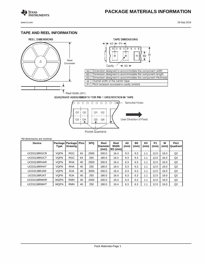
TAPE AND REEL INFORMATION
*All dimensions are nominal
Device PackageType
PackageDrawing
Pins SPQ ReelDiameter
(mm)
ReelWidth
W1 (mm)
A0(mm)
B0(mm)
K0(mm)
P1(mm)
W(mm)
Pin1Quadrant
UCD3138RGCR VQFN RGC 64 2000 330.0 16.4 9.3 9.3 1.1 12.0 16.0 Q2
UCD3138RGCT VQFN RGC 64 250 180.0 16.4 9.3 9.3 1.1 12.0 16.0 Q2
UCD3138RHAR VQFN RHA 40 2500 330.0 16.4 6.3 6.3 1.1 12.0 16.0 Q2
UCD3138RHAT VQFN RHA 40 250 180.0 16.4 6.3 6.3 1.1 12.0 16.0 Q2
UCD3138RJAR VQFN RJA 40 3000 330.0 16.4 6.3 6.3 1.1 12.0 16.0 Q2
UCD3138RJAT VQFN RJA 40 250 180.0 16.4 6.3 6.3 1.1 12.0 16.0 Q2
UCD3138RMHR WQFN RMH 40 2000 330.0 16.4 6.3 6.3 1.1 12.0 16.0 Q2
UCD3138RMHT WQFN RMH 40 250 180.0 16.4 6.3 6.3 1.1 12.0 16.0 Q2
PACKAGE MATERIALS INFORMATION
www.ti.com 29-Sep-2019
Pack Materials-Page 1

*All dimensions are nominal
Device Package Type Package Drawing Pins SPQ Length (mm) Width (mm) Height (mm)
UCD3138RGCR VQFN RGC 64 2000 367.0 367.0 38.0
UCD3138RGCT VQFN RGC 64 250 210.0 185.0 35.0
UCD3138RHAR VQFN RHA 40 2500 367.0 367.0 38.0
UCD3138RHAT VQFN RHA 40 250 210.0 185.0 35.0
UCD3138RJAR VQFN RJA 40 3000 367.0 367.0 38.0
UCD3138RJAT VQFN RJA 40 250 210.0 185.0 35.0
UCD3138RMHR WQFN RMH 40 2000 367.0 367.0 38.0
UCD3138RMHT WQFN RMH 40 250 210.0 185.0 35.0
PACKAGE MATERIALS INFORMATION
www.ti.com 29-Sep-2019
Pack Materials-Page 2

www.ti.com
GENERIC PACKAGE VIEW
Images above are just a representation of the package family, actual package may vary.Refer to the product data sheet for package details.
VQFN - 1 mm max heightRGC 64PLASTIC QUAD FLATPACK - NO LEAD9 x 9, 0.5 mm pitch
4224597/A
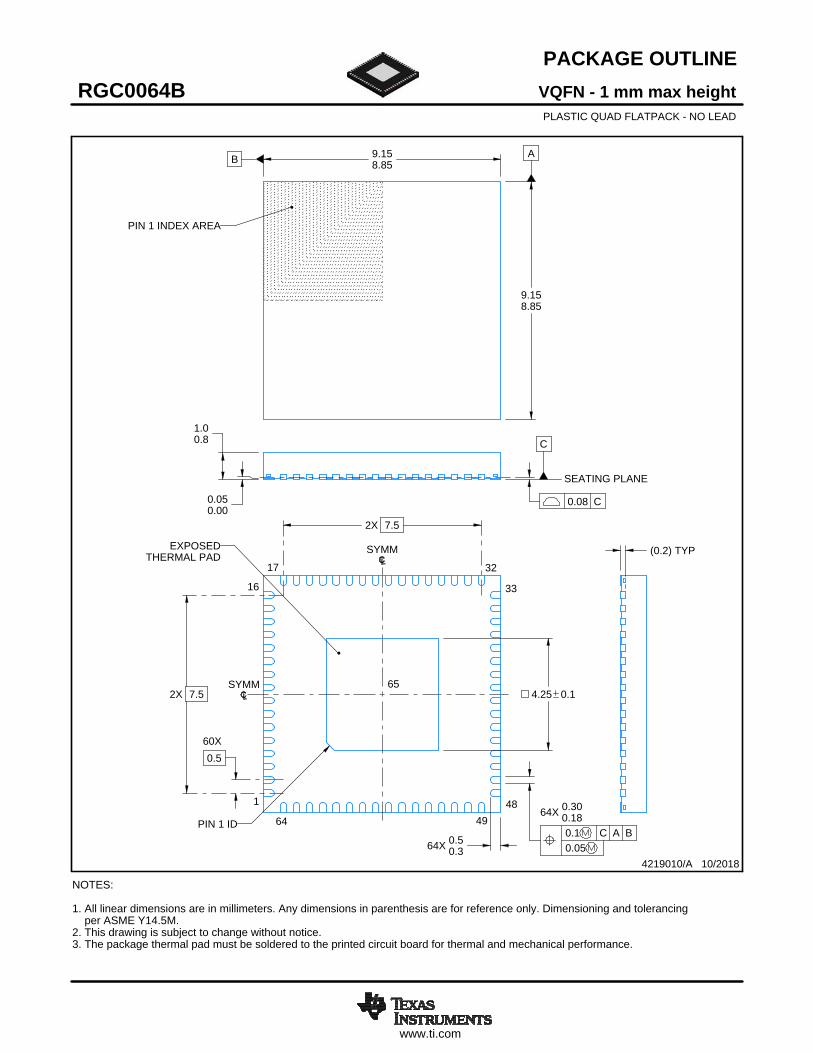
www.ti.com
PACKAGE OUTLINE
C
9.158.85
9.158.85
1.00.8
0.050.00
2X 7.5
60X0.5
2X 7.5
64X 0.50.3
64X 0.300.18
4.25 0.1
(0.2) TYP
VQFN - 1 mm max heightRGC0064BPLASTIC QUAD FLATPACK - NO LEAD
4219010/A 10/2018
0.08 C
0.1 C A B0.05
NOTES: 1. All linear dimensions are in millimeters. Any dimensions in parenthesis are for reference only. Dimensioning and tolerancing per ASME Y14.5M. 2. This drawing is subject to change without notice. 3. The package thermal pad must be soldered to the printed circuit board for thermal and mechanical performance.
PIN 1 INDEX AREA
SEATING PLANE
PIN 1 ID
SYMMEXPOSEDTHERMAL PAD
SYMM
1
16
17 32
33
484964
65
SCALE 1.500
AB

www.ti.com
EXAMPLE BOARD LAYOUT
60X (0.5)
(R0.05) TYP
0.07 MAXALL AROUND
0.07 MINALL AROUND
(0.695) TYP(1.18) TYP
(0.695) TYP
(1.18) TYP
64X (0.6)
64X (0.24)
(8.8)
(8.8)
( 4.25)
( 0.2) TYPVIA
VQFN - 1 mm max heightRGC0064BPLASTIC QUAD FLATPACK - NO LEAD
4219010/A 10/2018
NOTES: (continued) 4. This package is designed to be soldered to a thermal pad on the board. For more information, see Texas Instruments literature number SLUA271 (www.ti.com/lit/slua271).5. Vias are optional depending on application, refer to device data sheet. If any vias are implemented, refer to their locations shown on this view. It is recommended that vias under paste be filled, plugged or tented.
SYMM
SYMM
LAND PATTERN EXAMPLEEXPOSED METAL SHOWN
SCALE: 10X
SEE SOLDER MASKDETAIL
1
16
17 32
33
48
4964
65
METAL EDGE
SOLDER MASKOPENING
EXPOSED METAL
METAL UNDERSOLDER MASK
SOLDER MASKOPENING
EXPOSEDMETAL
NON SOLDER MASKDEFINED
(PREFERRED)SOLDER MASK DEFINED
SOLDER MASK DETAILS

www.ti.com
EXAMPLE STENCIL DESIGN
64X (0.6)
64X (0.24)
60X (0.5)
(8.8)
(8.8)
9X ( 1.19)(R0.05) TYP
(1.39)
(1.39)
VQFN - 1 mm max heightRGC0064BPLASTIC QUAD FLATPACK - NO LEAD
4219010/A 10/2018
NOTES: (continued) 6. Laser cutting apertures with trapezoidal walls and rounded corners may offer better paste release. IPC-7525 may have alternate design recommendations.
SOLDER PASTE EXAMPLEBASED ON 0.125 MM THICK STENCIL
SCALE: 10X
EXPOSED PAD 6571% PRINTED SOLDER COVERAGE BY AREA UNDER PACKAGE
SYMM
SYMM
1
16
17 32
33
48
4964
65

www.ti.com
GENERIC PACKAGE VIEW
This image is a representation of the package family, actual package may vary.Refer to the product data sheet for package details.
VQFN - 1 mm max heightRHA 40PLASTIC QUAD FLATPACK - NO LEAD6 x 6, 0.5 mm pitch
4225870/A
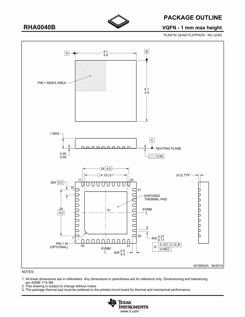
www.ti.com
PACKAGE OUTLINE
C
40X 0.270.17
4.15 0.1
40X 0.50.3
1 MAX
(0.2) TYP
0.050.00
2X4.5
36X 0.5
2X 4.5
A 6.15.9
B
6.15.9
VQFN - 1 mm max heightRHA0040BPLASTIC QUAD FLATPACK - NO LEAD
4219052/A 06/2016
PIN 1 INDEX AREA
0.08
SEATING PLANE
1
1021
30
11 20
40 31(OPTIONAL)PIN 1 ID 0.1 C A B
0.05
EXPOSEDTHERMAL PAD
41 SYMM
SYMM
NOTES: 1. All linear dimensions are in millimeters. Any dimensions in parenthesis are for reference only. Dimensioning and tolerancing per ASME Y14.5M. 2. This drawing is subject to change without notice. 3. The package thermal pad must be soldered to the printed circuit board for thermal and mechanical performance.
SCALE 2.200

www.ti.com
EXAMPLE BOARD LAYOUT
(1.14)TYP
0.07 MINALL SIDES
0.07 MAXALL AROUND
40X (0.22)
40X (0.6)
( 0.2) TYPVIA
( 4.15)
(R0.05) TYP
(5.8)
36X (0.5)
(5.8)(0.685)TYP
(1.14)TYP
(0.685)TYP
(0.25) TYP
VQFN - 1 mm max heightRHA0040BPLASTIC QUAD FLATPACK - NO LEAD
4219052/A 06/2016
SYMM
1
10
11 20
21
30
3140
SYMM
LAND PATTERN EXAMPLESCALE:12X
41
NOTES: (continued) 4. This package is designed to be soldered to a thermal pad on the board. For more information, see Texas Instruments literature number SLUA271 (www.ti.com/lit/slua271).
SOLDER MASKOPENING
METAL UNDERSOLDER MASK
SOLDER MASKDEFINED
METAL
SOLDER MASKOPENING
SOLDER MASK DETAILS
NON SOLDER MASKDEFINED
(PREFERRED)

www.ti.com
EXAMPLE STENCIL DESIGN
(1.37) TYP
(1.37)TYP
40X (0.6)
40X (0.22)
9X ( 1.17)
(R0.05) TYP
(5.8)
(5.8)
36X (0.5)
(0.25) TYP
VQFN - 1 mm max heightRHA0040BPLASTIC QUAD FLATPACK - NO LEAD
4219052/A 06/2016
NOTES: (continued) 5. Laser cutting apertures with trapezoidal walls and rounded corners may offer better paste release. IPC-7525 may have alternate design recommendations.
SYMM
METALTYP
SOLDER PASTE EXAMPLEBASED ON 0.125 mm THICK STENCIL
EXPOSED PAD 41:
72% PRINTED SOLDER COVERAGE BY AREA UNDER PACKAGESCALE:12X
SYMM
1
10
11 20
21
30
31
41
40

www.ti.com
PACKAGE OUTLINE
C
40X 0.300.18
4.15 0.1
40X 0.50.3
1 MAX
(0.2) TYP
0.050.00
2X4.5
36X 0.5
2X 4.5
4X ( 0.32)
2.74TYP
2.74 TYP
A 6.15.9
B
6.15.9
VQFN - 1 mm max heightRJA0040APLASTIC QUAD FLATPACK - NO LEAD
4222901/A 05/2016
PIN 1 INDEX AREA
0.08
SEATING PLANE
1
1021
30
11 20
40 31(OPTIONAL)PIN 1 ID 0.1 C A B
0.05
EXPOSEDTHERMAL PAD
A1
A2A3
A4
41
NOTES: 1. All linear dimensions are in millimeters. Any dimensions in parenthesis are for reference only. Dimensioning and tolerancing per ASME Y14.5M. 2. This drawing is subject to change without notice. 3. The package thermal pad must be soldered to the printed circuit board for thermal and mechanical performance.
SCALE 2.000

www.ti.com
EXAMPLE BOARD LAYOUT
(1.14)TYP
(2.74) TYP
(2.74)TYP
0.05 MINALL SIDES
0.05 MAXALL AROUND
40X (0.24)
40X (0.6)
( 0.2) TYPVIA
( 4.15)
(R0.05) TYP
(5.8)
36X (0.5)
4X ( 0.32)
(5.8)(0.685)
TYP
(1.14)TYP
(0.685)TYP
(0.25) TYP
VQFN - 1 mm max heightRJA0040APLASTIC QUAD FLATPACK - NO LEAD
4222901/A 05/2016
SYMM
1
10
11 20
21
30
3140
SYMM
LAND PATTERN EXAMPLESCALE:12X
41
A1
A2
A4
A3
NOTES: (continued) 4. This package is designed to be soldered to a thermal pad on the board. For more information, see Texas Instruments literature number SLUA271 (www.ti.com/lit/slua271).
SOLDER MASKOPENING
METAL UNDERSOLDER MASK
SOLDER MASKDEFINED
METAL
SOLDER MASKOPENING
SOLDER MASK DETAILS
NON SOLDER MASKDEFINED
(PREFERRED)

www.ti.com
EXAMPLE STENCIL DESIGN
4X ( 0.32)(1.37) TYP
(1.37)TYP
40X (0.6)
40X (0.24)
9X ( 1.17)
(R0.05) TYP
(5.8)
(5.8)
36X (0.5)
(0.25) TYP
VQFN - 1 mm max heightRJA0040APLASTIC QUAD FLATPACK - NO LEAD
4222901/A 05/2016
NOTES: (continued) 5. Laser cutting apertures with trapezoidal walls and rounded corners may offer better paste release. IPC-7525 may have alternate design recommendations.
41
A1
A2
A4
A3
SYMMMETALTYP
SOLDER PASTE EXAMPLEBASED ON 0.125 mm THICK STENCIL
EXPOSED PAD 41:
72% PRINTED SOLDER COVERAGE BY AREA UNDER PACKAGESCALE:12X
SYMM
1
10
11 20
21
30
3140


IMPORTANT NOTICE AND DISCLAIMERTI PROVIDES TECHNICAL AND RELIABILITY DATA (INCLUDING DATASHEETS), DESIGN RESOURCES (INCLUDING REFERENCEDESIGNS), APPLICATION OR OTHER DESIGN ADVICE, WEB TOOLS, SAFETY INFORMATION, AND OTHER RESOURCES “AS IS”AND WITH ALL FAULTS, AND DISCLAIMS ALL WARRANTIES, EXPRESS AND IMPLIED, INCLUDING WITHOUT LIMITATION ANYIMPLIED WARRANTIES OF MERCHANTABILITY, FITNESS FOR A PARTICULAR PURPOSE OR NON-INFRINGEMENT OF THIRDPARTY INTELLECTUAL PROPERTY RIGHTS.These resources are intended for skilled developers designing with TI products. You are solely responsible for (1) selecting the appropriateTI products for your application, (2) designing, validating and testing your application, and (3) ensuring your application meets applicablestandards, and any other safety, security, or other requirements. These resources are subject to change without notice. TI grants youpermission to use these resources only for development of an application that uses the TI products described in the resource. Otherreproduction and display of these resources is prohibited. No license is granted to any other TI intellectual property right or to any third partyintellectual property right. TI disclaims responsibility for, and you will fully indemnify TI and its representatives against, any claims, damages,costs, losses, and liabilities arising out of your use of these resources.TI’s products are provided subject to TI’s Terms of Sale (https:www.ti.com/legal/termsofsale.html) or other applicable terms available eitheron ti.com or provided in conjunction with such TI products. TI’s provision of these resources does not expand or otherwise alter TI’sapplicable warranties or warranty disclaimers for TI products.IMPORTANT NOTICE
Mailing Address: Texas Instruments, Post Office Box 655303, Dallas, Texas 75265Copyright © 2021, Texas Instruments Incorporated