
UART DESIGN, INTEGRATION AND SYNTHESIS ON …eprints.utar.edu.my/2257/1/CT-2016-1203260-1.pdfUART...
124
UART DESIGN, INTEGRATION AND SYNTHESIS ON FPGA BY LEE ZHI YONG A REPORT SUBMITTED TO Universiti Tunku Abdul Rahman in partial fulfillment of the requirements for the degree of BACHELOR OF INFORMATION TECHNOLOGY (HONS) COMPUTER ENGINEERING Faculty of Information and Communication Technology (Perak Campus) MAY 2016
Transcript of UART DESIGN, INTEGRATION AND SYNTHESIS ON …eprints.utar.edu.my/2257/1/CT-2016-1203260-1.pdfUART...
UART DESIGN, INTEGRATION AND SYNTHESIS ON FPGA
BY
LEE ZHI YONG
A REPORT
SUBMITTED TO
Universiti Tunku Abdul Rahman
in partial fulfillment of the requirements
for the degree of
BACHELOR OF INFORMATION TECHNOLOGY (HONS)
COMPUTER ENGINEERING
Faculty of Information and Communication Technology
(Perak Campus)
MAY 2016

CHAPTER 1: INTRODUCTION
UNIVERSITI TUNKU ABDUL RAHMAN
REPORT STATUS DECLARATION FORM
Title : __________________________________________________________
__________________________________________________________
__________________________________________________________
Academic Session: _____________
I __________________________________________________________
(CAPITAL LETTER)
declare that I allow this Final Year Project Report to be kept in
Universiti Tunku Abdul Rahman Library subject to the regulations as follows:
1. The dissertation is a property of the Library.
2. The Library is allowed to make copies of this dissertation for academic purposes.
Verified by,
_________________________ _________________________
(Author’s signature) (Supervisor’s signature)
Address:
__________________________
__________________________ _________________________
__________________________ Supervisor’s name
Date: _____________________ Date: ____________________

CHAPTER 1: INTRODUCTION
UART DESIGN, INTEGRATION AND SYNTHESIS ON FPGA
BY
LEE ZHI YONG
A REPORT
SUBMITTED TO
Universiti Tunku Abdul Rahman
in partial fulfillment of the requirements
for the degree of
BACHELOR OF INFORMATION TECHNOLOGY (HONS)
COMPUTER ENGINEERING
Faculty of Information and Communication Technology
(Perak Campus)
MAY 2016

CHAPTER 1: INTRODUCTION

CHAPTER 1: INTRODUCTION
ii BIT (Hons) Computer Engineering Faculty of Information and Communication Technology (Perak Campus), UART
DECLARATION OF ORIGINALITY
I declare that this report entitled "UART DESIGN, INTEGRATION AND
SYNTHESIS ON FPGA" is my own work except as cited in the references. The
report has not been accepted for any degree and is not being submitted concurrently in
candidature for any degree or other award.
Signature : ______________________
Name : ______________________
Date : ______________________
CHAPTER 1: INTRODUCTION
iii BIT (Hons) Computer Engineering Faculty of Information and Communication Technology (Perak Campus), UART
ACKNOWLEDGEMENTS
First of all, I would like express deepest gratitude to my project supervisor, Mr. Mok
Kai Ming who has been providing me invaluable guidance and constructive
suggestions throughout the planning and development of this project.
I would also like to express my appreciation to my family members who have been
giving me endless support and encouragement since the starting of my undergraduate
years. Nevertheless, I would like to thank all my course mates and friends who
supported my throughout the entire course of this project.
Once again, I appreciate all the guidance and generous support that provided by
people I have mentioned above. All the supports and helps contribute to the
accomplishment of this project.
CHAPTER 1: INTRODUCTION
iv BIT (Hons) Computer Engineering Faculty of Information and Communication Technology (Perak Campus), UART
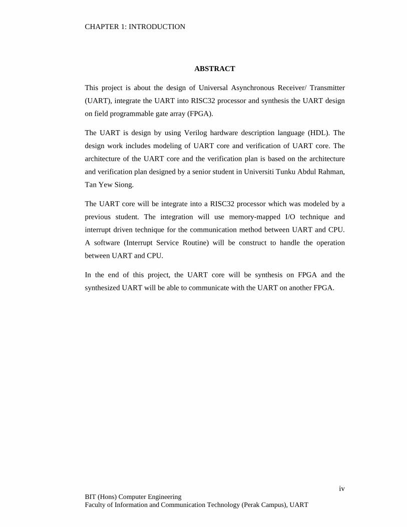
ABSTRACT
This project is about the design of Universal Asynchronous Receiver/ Transmitter
(UART), integrate the UART into RISC32 processor and synthesis the UART design
on field programmable gate array (FPGA).
The UART is design by using Verilog hardware description language (HDL). The
design work includes modeling of UART core and verification of UART core. The
architecture of the UART core and the verification plan is based on the architecture
and verification plan designed by a senior student in Universiti Tunku Abdul Rahman,
Tan Yew Siong.
The UART core will be integrate into a RISC32 processor which was modeled by a
previous student. The integration will use memory-mapped I/O technique and
interrupt driven technique for the communication method between UART and CPU.
A software (Interrupt Service Routine) will be construct to handle the operation
between UART and CPU.
In the end of this project, the UART core will be synthesis on FPGA and the
synthesized UART will be able to communicate with the UART on another FPGA.
CHAPTER 1: INTRODUCTION
v BIT (Hons) Computer Engineering Faculty of Information and Communication Technology (Perak Campus), UART
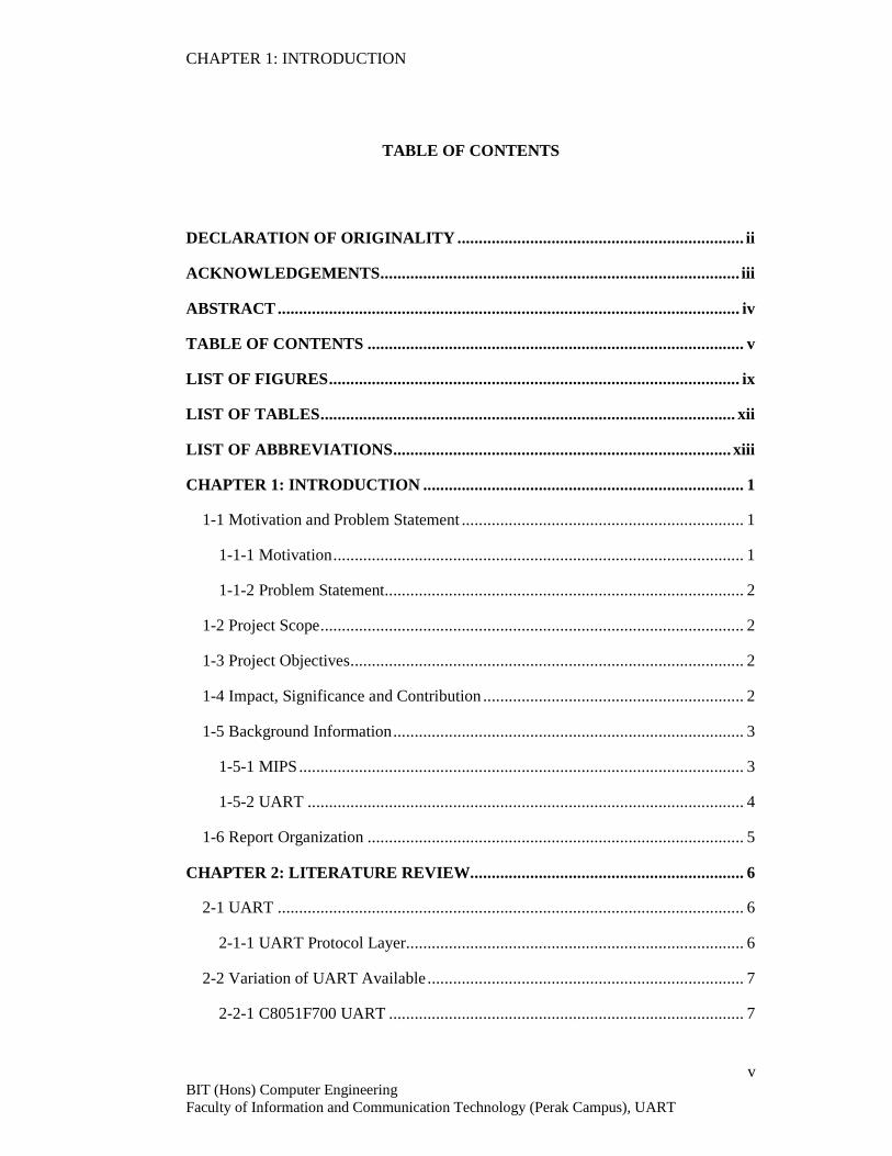
TABLE OF CONTENTS
DECLARATION OF ORIGINALITY ......................... .......................................... ii
ACKNOWLEDGEMENTS.................................................................................... iii
ABSTRACT............................................................................................................ iv
TABLE OF CONTENTS ........................................................................................ v
LIST OF FIGURES................................................................................................ ix
LIST OF TABLES................................................................................................. xii
LIST OF ABBREVIATIONS............................................................................... xiii
CHAPTER 1: INTRODUCTION ........................................................................... 1
1-1 Motivation and Problem Statement ..................................................................1
1-1-1 Motivation................................................................................................ 1
1-1-2 Problem Statement.................................................................................... 2
1-2 Project Scope................................................................................................... 2
1-3 Project Objectives............................................................................................ 2
1-4 Impact, Significance and Contribution .............................................................2
1-5 Background Information.................................................................................. 3
1-5-1 MIPS........................................................................................................ 3
1-5-2 UART ...................................................................................................... 4
1-6 Report Organization ........................................................................................ 5
CHAPTER 2: LITERATURE REVIEW ................................................................ 6
2-1 UART ............................................................................................................. 6
2-1-1 UART Protocol Layer............................................................................... 6
2-2 Variation of UART Available.......................................................................... 7
2-2-1 C8051F700 UART ................................................................................... 7

CHAPTER 1: INTRODUCTION
vi BIT (Hons) Computer Engineering Faculty of Information and Communication Technology (Perak Campus), UART
2-2-2 UART (Digital System Design Using VHDL, by Charles H. Roth)........... 8
2-2-3 UART (by Tan Yew Siong) .................................................................... 10
2-3 MIPS Memory Map....................................................................................... 10
2-4 Exception Handler and Interrupt Service Routine (ISR) ................................. 13
CHAPTER 3: PROPOSED METHOD AND APPROACH................................. 15
3-1 Design Specifications .................................................................................... 15
3-1-1 Design Methodology ..............................................................................15
3-1-2 Design Tools .......................................................................................... 17
CHAPTER 4: SYSTEM SPECIFICATION......................................................... 20
4-1 Naming Convention....................................................................................... 20
4-2 Integration of UART into RISC32 processor ................................................. 21
4-2-1 RISC32 Processor Interface .................................................................... 21
4-2-2 Input Pin Description.............................................................................. 21
4-2-3 Output Pin Description ........................................................................... 22
CHAPTER 5: MICRO-ARCHITECTURE SPECIFICATION (UNIT L EVEL)24
5-1 Micro-Architecture of RISC32 Microprocessor ............................................. 24
5-2 Design Hierarchy........................................................................................... 25
5-3 Datapath Unit ................................................................................................ 27
5-3-1 Datapath Unit Interface........................................................................... 27
5-4 Control Path Unit........................................................................................... 28
5-4-1 Control Path Unit Interface.....................................................................28
5-5 Memory Unit ................................................................................................. 29
5-5-1 Memory Unit Interface ...........................................................................29
5-6 UART Unit.................................................................................................... 29
5-6-1 Operating Procedure ............................................................................... 29
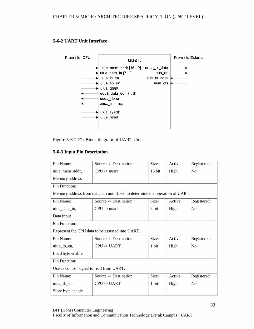
5-6-2 UART Unit Interface .............................................................................. 33
5-6-3 Input Pin Description.............................................................................. 33
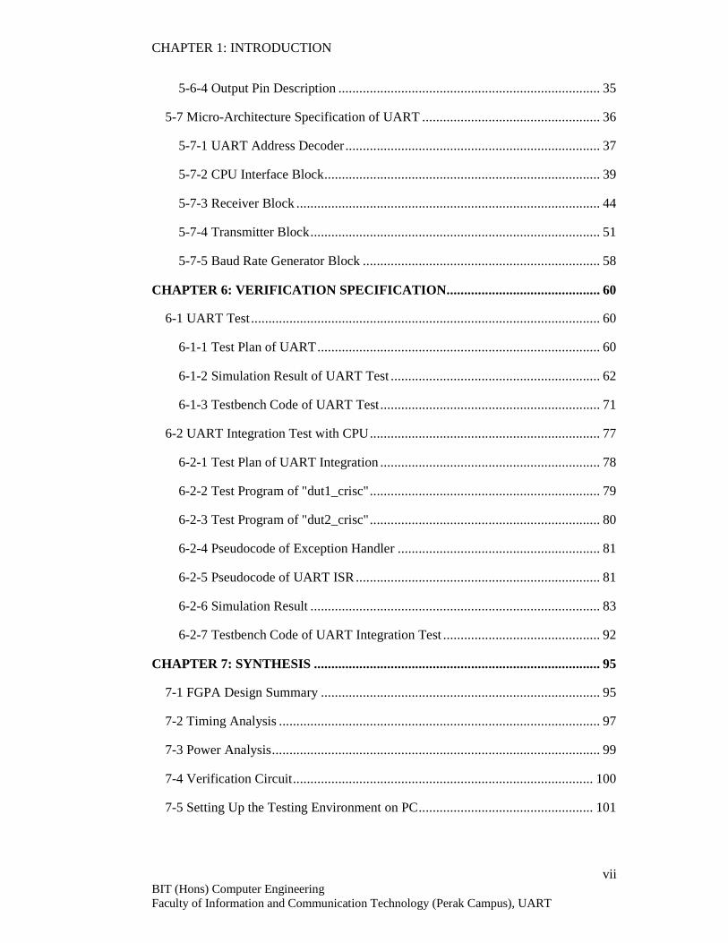
CHAPTER 1: INTRODUCTION
vii BIT (Hons) Computer Engineering Faculty of Information and Communication Technology (Perak Campus), UART
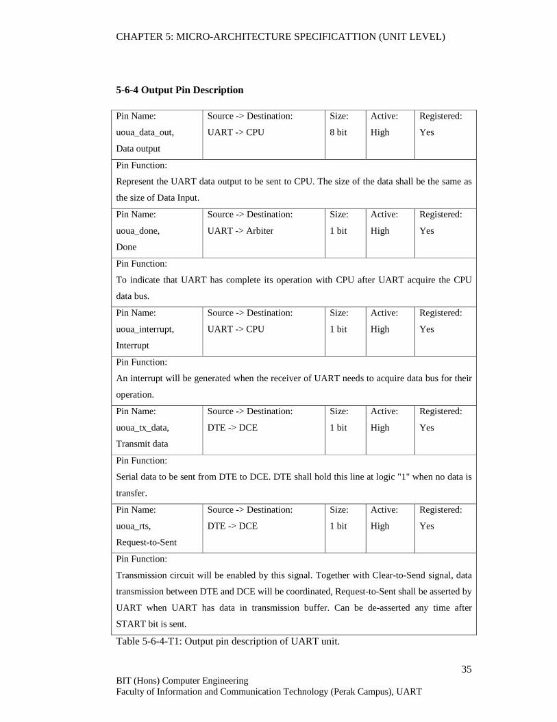
5-6-4 Output Pin Description ........................................................................... 35
5-7 Micro-Architecture Specification of UART ................................................... 36
5-7-1 UART Address Decoder......................................................................... 37
5-7-2 CPU Interface Block............................................................................... 39
5-7-3 Receiver Block ....................................................................................... 44
5-7-4 Transmitter Block................................................................................... 51
5-7-5 Baud Rate Generator Block .................................................................... 58
CHAPTER 6: VERIFICATION SPECIFICATION.............. .............................. 60
6-1 UART Test.................................................................................................... 60
6-1-1 Test Plan of UART................................................................................. 60
6-1-2 Simulation Result of UART Test ............................................................ 62
6-1-3 Testbench Code of UART Test............................................................... 71
6-2 UART Integration Test with CPU.................................................................. 77
6-2-1 Test Plan of UART Integration ............................................................... 78
6-2-2 Test Program of "dut1_crisc".................................................................. 79
6-2-3 Test Program of "dut2_crisc".................................................................. 80
6-2-4 Pseudocode of Exception Handler .......................................................... 81
6-2-5 Pseudocode of UART ISR...................................................................... 81
6-2-6 Simulation Result ................................................................................... 83
6-2-7 Testbench Code of UART Integration Test ............................................. 92
CHAPTER 7: SYNTHESIS ..................................................................................95
7-1 FGPA Design Summary ................................................................................ 95
7-2 Timing Analysis ............................................................................................ 97
7-3 Power Analysis.............................................................................................. 99
7-4 Verification Circuit...................................................................................... 100
7-5 Setting Up the Testing Environment on PC.................................................. 101
CHAPTER 1: INTRODUCTION
viii BIT (Hons) Computer Engineering Faculty of Information and Communication Technology (Perak Campus), UART
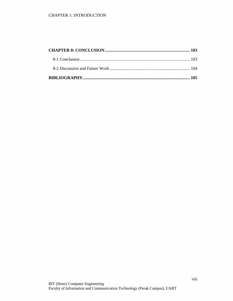
CHAPTER 8: CONCLUSION............................................................................ 103
8-1 Conclusion .................................................................................................. 103
8-2 Discussion and Future Work........................................................................104
BIBLIOGRAPHY................................................................................................ 105
CHAPTER 1: INTRODUCTION
ix BIT (Hons) Computer Engineering Faculty of Information and Communication Technology (Perak Campus), UART
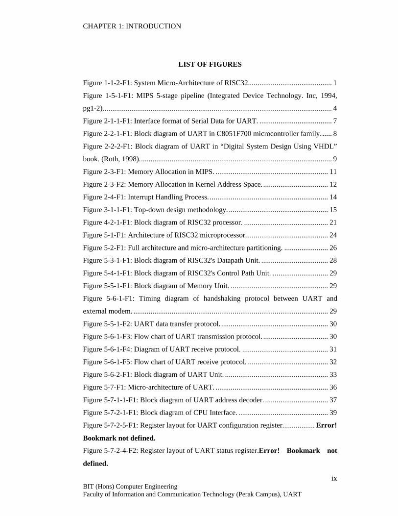
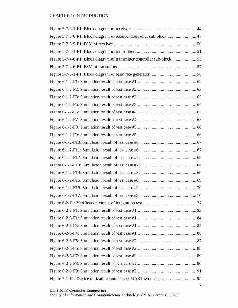
LIST OF FIGURES
Figure 1-1-2-F1: System Micro-Architecture of RISC32............................................ 1
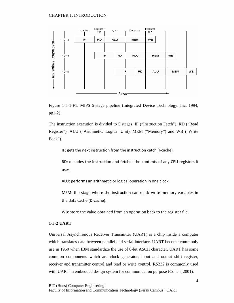
Figure 1-5-1-F1: MIPS 5-stage pipeline (Integrated Device Technology. Inc, 1994,
pg1-2)........................................................................................................................ 4
Figure 2-1-1-F1: Interface format of Serial Data for UART. ...................................... 7
Figure 2-2-1-F1: Block diagram of UART in C8051F700 microcontroller family...... 8
Figure 2-2-2-F1: Block diagram of UART in “Digital System Design Using VHDL”
book. (Roth, 1998)..................................................................................................... 9
Figure 2-3-F1: Memory Allocation in MIPS. ........................................................... 11
Figure 2-3-F2: Memory Allocation in Kernel Address Space................................... 12
Figure 2-4-F1: Interrupt Handling Process. .............................................................. 14
Figure 3-1-1-F1: Top-down design methodology. .................................................... 15
Figure 4-2-1-F1: Block diagram of RISC32 processor............................................. 21
Figure 5-1-F1: Architecture of RISC32 microprocessor. .......................................... 24
Figure 5-2-F1: Full architecture and micro-architecture partitioning. ....................... 26
Figure 5-3-1-F1: Block diagram of RISC32's Datapath Unit. ................................... 28
Figure 5-4-1-F1: Block diagram of RISC32's Control Path Unit. ............................. 29
Figure 5-5-1-F1: Block diagram of Memory Unit. ................................................... 29
Figure 5-6-1-F1: Timing diagram of handshaking protocol between UART and
external modem. ...................................................................................................... 29
Figure 5-5-1-F2: UART data transfer protocol. ........................................................ 30
Figure 5-6-1-F3: Flow chart of UART transmission protocol. .................................. 30
Figure 5-6-1-F4: Diagram of UART receive protocol. ............................................. 31
Figure 5-6-1-F5: Flow chart of UART receive protocol. .......................................... 32
Figure 5-6-2-F1: Block diagram of UART Unit. ...................................................... 33
Figure 5-7-F1: Micro-architecture of UART. ........................................................... 36
Figure 5-7-1-1-F1: Block diagram of UART address decoder. ................................. 37
Figure 5-7-2-1-F1: Block diagram of CPU Interface. ............................................... 39
Figure 5-7-2-5-F1: Register layout for UART configuration register.................Error!
Bookmark not defined.
Figure 5-7-2-4-F2: Register layout of UART status register.Error! Bookmark not
defined.
CHAPTER 1: INTRODUCTION
x BIT (Hons) Computer Engineering Faculty of Information and Communication Technology (Perak Campus), UART
Figure 5-7-3-1-F1: Block diagram of receiver..........................................................44
Figure 5-7-3-6-F1: Block diagram of receiver controller sub-block.......................... 47
Figure 5-7-3-9-F1: FSM of receiver......................................................................... 50
Figure 5-7-4-1-F1: Block diagram of transmitter. .................................................... 51
Figure 5-7-4-6-F1: Block diagram of transmitter controller sub-block. .................... 55
Figure 5-7-4-6-F1: FSM of transmitter..................................................................... 57
Figure 5-7-5-1-F1: Block diagram of baud rate generator. ....................................... 58
Figure 6-1-2-F1: Simulation result of test case #1....................................................62
Figure 6-1-2-F2: Simulation result of test case #2....................................................63
Figure 6-1-2-F3: Simulation result of test case #2....................................................63
Figure 6-1-2-F5: Simulation result of test case #3....................................................64
Figure 6-1-2-F6: Simulation result of test case #4....................................................65
Figure 6-1-2-F7: Simulation result of test case #4....................................................65
Figure 6-1-2-F8: Simulation result of test case #5....................................................66
Figure 6-1-2-F9: Simulation result of test case #5....................................................66
Figure 6-1-2-F10: Simulation result of test case #6. ................................................. 67
Figure 6-1-2-F11: Simulation result of test case #6. ................................................. 67
Figure 6-1-2-F12: Simulation result of test case #7.................................................. 68
Figure 6-1-2-F13: Simulation result of test case #7. ................................................. 68
Figure 6-1-2-F14: Simulation result of test case #8. ................................................. 69
Figure 6-1-2-F15: Simulation result of test case #8. ................................................. 69
Figure 6-1-2-F16: Simulation result of test case #9. ................................................. 70
Figure 6-1-2-F17: Simulation result of test case #9. ................................................. 70
Figure 6-2-F1: Verification circuit of integration test. ..............................................77
Figure 6-2-6-F1: Simulation result of test case #1....................................................83
Figure 6-2-6-F1: Simulation result of test case #1....................................................84
Figure 6-2-6-F3: Simulation result of test case #1....................................................85
Figure 6-2-6-F4: Simulation result of test case #1....................................................86
Figure 6-2-6-F5: Simulation result of test case #2....................................................87
Figure 6-2-6-F6: Simulation result of test case #2....................................................88
Figure 6-2-6-F7: Simulation result of test case #2....................................................89
Figure 6-2-6-F8: Simulation result of rest case #2....................................................90
Figure 6-2-6-F9: Simulation result of test case #2....................................................91
Figure 7-1-F1: Device utilization summary of UART synthesis. .............................. 95

CHAPTER 1: INTRODUCTION
xi BIT (Hons) Computer Engineering Faculty of Information and Communication Technology (Perak Campus), UART
Figure 7-1-F2: IO pin report of UART synthesis...................................................... 96
Figure 7-3-F1: Power analysis report of UART synthesis. ....................................... 99
Figure 7-4-F1: Block diagram of UART verification circuit................................... 100
Figure 7-5-F1: Configuration settings of serial com. on Tera Term. ....................... 102
CHAPTER 1: INTRODUCTION
xii BIT (Hons) Computer Engineering Faculty of Information and Communication Technology (Perak Campus), UART
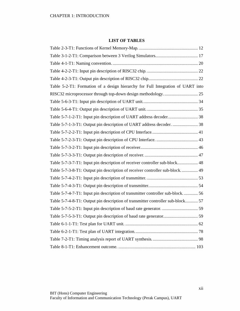
LIST OF TABLES
Table 2-3-T1: Functions of Kernel Memory-Map. ................................................... 12
Table 3-1-2-T1: Comparison between 3 Verilog Simulators..................................... 17
Table 4-1-T1: Naming convention. .......................................................................... 20
Table 4-2-2-T1: Input pin description of RISC32 chip. ............................................ 22
Table 4-2-3-T1: Output pin description of RISC32 chip........................................... 22
Table 5-2-T1: Formation of a design hierarchy for Full Integration of UART into
RISC32 microprocessor through top-down design methodology. ............................. 25
Table 5-6-3-T1: Input pin description of UART unit................................................ 34
Table 5-6-4-T1: Output pin description of UART unit. ............................................ 35
Table 5-7-1-2-T1: Input pin description of UART address decoder.......................... 38
Table 5-7-1-3-T1: Output pin description of UART address decoder. ...................... 38
Table 5-7-2-2-T1: Input pin description of CPU Interface........................................ 41
Table 5-7-2-3-T1: Output pin description of CPU Interface. .................................... 43
Table 5-7-3-2-T1: Input pin description of receiver.................................................. 46
Table 5-7-3-3-T1: Output pin description of receiver. .............................................. 47
Table 5-7-3-7-T1: Input pin description of receiver controller sub-block.................. 48
Table 5-7-3-8-T1: Output pin description of receiver controller sub-block. .............. 49
Table 5-7-4-2-T1: Input pin description of transmitter. ............................................ 53
Table 5-7-4-3-T1: Output pin description of transmitter........................................... 54
Table 5-7-4-7-T1: Input pin description of transmitter controller sub-block. ............ 56
Table 5-7-4-8-T1: Output pin description of transmitter controller sub-block........... 57
Table 5-7-5-2-T1: Input pin description of baud rate generator. ............................... 59
Table 5-7-5-3-T1: Output pin description of baud rate generator.............................. 59
Table 6-1-1-T1: Test plan for UART unit. ............................................................... 62
Table 6-2-1-T1: Test plan of UART integration....................................................... 78
Table 7-2-T1: Timing analysis report of UART synthesis. ....................................... 98
Table 8-1-T1: Enhancement outcome. ................................................................... 103

CHAPTER 1: INTRODUCTION
xiii BIT (Hons) Computer Engineering Faculty of Information and Communication Technology (Perak Campus), UART
LIST OF ABBREVIATIONS
UART Universal Asynchronous Receiver Transmitter
FPGA Field Programmable Gate Array
IP Intellectual Property
IC Integrated Circuit
I/O Input Output
ISA Instruction Set Architecture
ISR Interrupt Service Routine
HDL Hardware Description Language
MIPS Microprocessor without Interlocked Pipeline Stages
RISC Reduced Instruction Set Computer
DTE Data Terminal Equipment (UART)
DCE Data Communication Equipment (External modem)
FSM Finite State Machine
CHAPTER 1: INTRODUCTION
1 BIT (Hons) Computer Engineering Faculty of Information and Communication Technology (Perak Campus), UART
CHAPTER 1: INTRODUCTION
1-1 Motivation and Problem Statement
1-1-1 Motivation
A 32-bit pipelined RISC microprocessor has been developed in Faculty of
Information and Communication Technology, UniversitiTunku Abdul Rahman
(UTAR) using Verilog which is a hardware description language (HDL). The project
is based on the Reduced Instruction Set Computing (RISC) architecture. The
motivations to initiate the project are due to following reasons:
Microchip design companies designed microprocessor as Intellectual Property or IP
for commercial purpose. The microprocessor IP includes information on the entire
design process for the front-end (modeling and verification) and back-end (physical
design) integrated circuit (IC) design. These are trade secrets of a company and
certainly not made available in the market at an affordable price for research purpose.
Several freely available microprocessor cores can be found in internet, most of them
can be found at OpenCores (http://www.opencores.org/). Unfortunately, these
processors do not implement the entire MIPS Instruction Set Architecture (ISA) and
lack comprehensive documentation. This makes them unsuitable for reuse and
customization.
The verification specification for a freely available RISC microprocessor core that is
available on the Internet is not well developed and incomplete. Therefore, without a
good verification specification, the verification process will be slow and hence, will
slow down the overall design process.
The lack of well-developed verification specifications for these microprocessor cores
will inevitably affect the physical design phase. A design needs to be functionally
proven before the physical design phase can proceed smoothly. Otherwise, if the
front-end design has to be changed, the physical design process has to be redone.
This project will aim to provide solutions to the above problems by creating a 32-bit
RISC core-based development environment to assist research work in the area of soft-
core and also application specific hardware modeling.
CHAPTER 1: INTRODUCTION
2 BIT (Hons) Computer Engineering Faculty of Information and Communication Technology (Perak Campus), UART
In RISC32 project, it is divided into several units based on the MIPS architecture. Up
to date, the RISC32 project that initiated in UTAR has completed the CPU designs
that support basic instructions similar to MIPS instructions. The system control
coprocessor, Coprocessor 0 (CP0) available as well to interface I/O device and handle
interrupt.
1-1-2 Problem Statement
So far, there is MIPS-compatible ISA which includes the Central Processing Unit
(CPU), PS/2 mouse system, PS/2 keyboard system, basic memory, coprocessor 0
(CP0), and Universal Asynchronous Receiver/Transmitter (UART). However, the
existing UART architecture and the Interrupt Service Routine (ISR) of UART are not
integrated in RISC32 yet. Hence, this project is initiated to synthesis the existing
UART and integrates the ISR into RISC32 processor. Figure 1-1-2-F1 shows the
system micro-architecture of RISC32.

CHAPTER 1: INTRODUCTION
1 BIT (Hons) Computer Engineering Faculty of Information and Communication Technology (Perak Campus), UART
Figure 1-1-2-F1: System Micro-Architecture of RISC32.
CHAPTER 1: INTRODUCTION
2 BIT (Hons) Computer Engineering Faculty of Information and Communication Technology (Perak Campus), UART
As shown in Figure 1-1-1, the bus arbiter is not implemented in the RISC32 processor
does not support multiple I/O, therefore the UART unit has to connect point-to-point
to bus system.
1-2 Project Scope
This project is aim to design an UART model with Verilog HDL. The specifications
of UART and its internal block will be developed and the functional behavior will be
verified by using test bench. The UART will be integrated into the existing RISC32
processor. An Interrupt Service Routine (ISR) will be developed to handle the data
received by UART.A test program will be written to test the functionality of the ISR.
Lastly, the UART will be synthesis on FGPA.
1-3 Project Objectives
There are several objectives in this project, they are:
• To design a UART and integrate it to the RISC32 processor.
• To develop the Interrupt Service Routine (ISR) into RISC32 processor.
• To synthesis the UART module on Field Programmable Gate Array (FPGA)
with completes documented timing and resource usage information.
• To develop a test bench to verify the UART functionality.
1-4 Impact, Significance and Contribution
As a conclusion of problem statement, there is lack of well-developed and well-
founded RISC32 processor available. After this project is done, it can provide a
complete RISC microprocessor core-based development environment and the
interface system that connects the UART to the microprocessor. The development
environment refers to the availability of the following:
• A well-developed design documentation of chip specification, architecture
specification and micro-architecture specification.
CHAPTER 1: INTRODUCTION
3 BIT (Hons) Computer Engineering Faculty of Information and Communication Technology (Perak Campus), UART
• A fully functional well-developed CPU UART Interfacing in the form of
synthesis-ready RTL written in Verilog.
• A well-developed verification specification of the UART. The verification
specification should contain suitable verification methodology, verification
techniques, test plan, test bench architecture etc.
• A complete physical design in FPGA with documented timing and resources
usage information.
This project is to develop an environment that mentioned above: to integrate the
multi-cycle pipelined RISC microprocessor core-based platform with the UART
which can support hardware modeling research work.
With the available well-developed basic RISC RTL model (which has been
functionally fully verified), the verification environment and the design documents, a
researcher will be able to develop their own research specific RTL model as part of
the MIPS environment and can quickly verify his model to obtain result.
Consequently, the research work could be done easier and speed up significantly.
1-5 Background Information
1-5-1 MIPS
MIPS also known as Microprocessor without Interlocked Pipelined Stage, which
based on the Reduced Instruction Set Computer (RISC) architecture is developed by a
team led by John L. Hennessy and David A. Patterson. The MIPS architecture can be
found in the book call Computer Organization and Design: The Hardware/ Software
Interface (Patterson and Hennessy, 2005). This book will show the architecture of
MIPS, the instruction and all the related stuff need to understand the function and
build a microprocessor. MIPS processors operate by breaking instruction execution
into multiple small independent stages (Integrated Device Technology. Inc, 1994,
pg1-2).
CHAPTER 1: INTRODUCTION
4 BIT (Hons) Computer Engineering Faculty of Information and Communication Technology (Perak Campus), UART
Figure 1-5-1-F1: MIPS 5-stage pipeline (Integrated Device Technology. Inc, 1994,
pg1-2).
The instruction execution is divided to 5 stages, IF (“Instruction Fetch”), RD (“Read
Register”), ALU (“Arithmetic/ Logical Unit), MEM (“Memory”) and WB (”Write
Back”).
IF: gets the next instruction from the instruction catch (I-cache).
RD: decodes the instruction and fetches the contents of any CPU registers it
uses.
ALU: performs an arithmetic or logical operation in one clock.
MEM: the stage where the instruction can read/ write memory variables in
the data cache (D-cache).
WB: store the value obtained from an operation back to the register file.
1-5-2 UART
Universal Asynchronous Receiver Transmitter (UART) is a chip inside a computer
which translates data between parallel and serial interface. UART become commonly
use in 1960 when IBM standardize the use of 8-bit ASCII character. UART has some
common components which are clock generator; input and output shift register,
receiver and transmitter control and read or write control. RS232 is commonly used
with UART in embedded design system for communication purpose (Cohen, 2001).
This report contain 9 chapters in total, which are introduction, literature review,
proposed method and approach, system specification, architecture specification,
micro-architecture specification, result and simulation, synthesis and conclusion.
In chapter 1, the motivation of this project is stated, follow by the problem statement,
project scope and objective, background of MIPS and UART and the flow of this
report.
In Literature Review chapter, the functions and protocol of UART is explained and 3
different UART model is discussed. For the next chapter Method Proposed and
Approach, shows the methodology used in this project and the technologies and tools
involved in the design phase of the UART.
Moving on to System specification chapter, in this chapter the top level of the design
is shown and described. The subsequence chapter shows the architecture of the top
level design and the pin in-out description. After that the micro-architecture of UART
is shown in the next chapter which is chapter 6, Micro-architecture specification.
The test result of UART and the integration test of UART is showed in Result and
Simulation chapter. The next chapter is Synthesis. This chapter shows the summary
report of synthesis and how the UART is tested. Finally the last chapter, Conclusion,
concludes the whole project and the future improvement that can be make to this
project is mentioned.

2-1 UART
UART is a serial communication device which consists two major blocks that is
receiver and transmitter. The device is asynchronous because the receiver and the
transmitter clock are not synchronized with each other. The word asynchronous
transmitter is base on the start and stop bit to receive or transmit data (Cohen, 2001).
Due to the asynchronous problem, a baud rate must be set to agree the operation
between receiver and transmitter. It will configure the clock to be 8 times faster than
the baud rate. Transmitter will start sending and the receiver will start receiving the
data when both transmitter terminal and receiver terminal are ready to process. Both
Receiver and Transmitter will check for error before proceed to process another data.
2-1-1 UART Protocol Layer
• START Bit: This bit is set to LOW to initiate bit synchronization of the
message at the receiver.
• Data Word: Represent the data that will be transmitted. The least significant
bit (LSB) will be sent out first follow by next bit until the most significant bit
(MSB).
• Parity Bit: This bit represents even or odd parity if parity is enable. The CPU
is in charge of manipulating the even or odd parity.
• STOP Bit: This bit is set to HIGH to provide message-framing indication for
use in bit synchronization at the receiver.
Figure 2-1-1-F1 shows the interface format of the serial data for UART.

2-2 Variation of UART Available
Three freely available UART core was used as benchmarking purpose. The first
UART core is C8051F700 UART by Silicon Labs. The second UART core is the
UART in a book, “Digital System Design Using VHDL” by Charles H. Roth. The last
UART core is a UART designed by a graduate student in UTAR, Tan Yew Siong.
The criteria of the benchmarking are documentation, the architecture and hardware
description language used to modeling the design.
2-2-1 C8051F700 UART
This UART can be found in C8051F700 microcontroller family. It consists of 3 main
blocks which is baud rate generator, transmitter and a receiver. Besides, it also
consists of 2 special function register (SFR) – SBUFx and SCONx. These special
function register are used to control and manage the serial communication. Figure 2-
2-1-F1 shows the block diagram of UART in C8051F700 microcontroller family. Due
to this UART is designed for commercial purpose, the design documents are not
available for free.

Figure 2-2-1-F1: Block diagram of UART in C8051F700 microcontroller family.
2-2-2 UART (Digital System Design Using VHDL, by Charles H. Roth)
This UART used VHDL hardware description language to design. It consists of three
main blocks in architecture level which is baud rate generator, receiver and
transmitter. There are 6 register in the UART,
• RSR : Receiver Shift Register
• RDR : Receiver Data Register
• TSR : Transmitter Shift Register
• TDR : Transmitter Data Register
• SCCR : Serial Communication Control Register
• SCSR : Serial Communication Status Register
The documentation of this UART includes the theory of how UART functioning and
the flow of how UART operate. Besides, the code for the UART module is also
available in the book, but there is no verification part describe in the book. Figure 2-2-
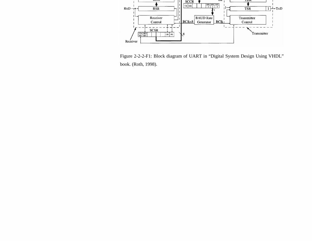
Figure 2-2-2-F1: Block diagram of UART in “Digital System Design Using VHDL”
book. (Roth, 1998).
The UART designed by Tan Yew Siong are well documented and it has verification
plan too. The design is modeled using Verilog HDL. The architecture of the UART is
more complicated where it contains CPU interface, clock generator, receiver,
transmitter, receiver FIFO and transmitter FIFO. The UART is successfully integrated
into RICS32 processor. The exception handler has been developed in this project too.
But it is not fully complete as it did not handle some cases, for example overflow
exception, breakpoint exception and address error exception.
2-3 MIPS Memory Map
The RISC32 uses a conventional memory layout that divides the memory into user
address space and kernel address space. A program’s address space consists of 3 parts
which is text segment, data segment and stack segment. The bottom of the user
address space, which is text segment, is used to stores program codes or instructions.
While the data segment divided into static data and dynamic data, the dynamic area
grows as memory is allocated to dynamic data structures. At the end of the user
address space, there is a stack segment which will grows downward towards the lower
memory address. This placement of segments allows sharing of unused memory by
both data and stack segments (Dandamudi, 2005). The following figure shows the
memory allocation:

Figure 2-3-F1: Memory Allocation in MIPS.
The address starting from 0x8000_0000 until the end of the memory map is the kernel
address space. Figure 2-3-F2 shows the memory allocation in kernel address space.
32’h0000 0000
Reserved
Program Code
(Instructions)
Static data
32’h0040 0000 (PC)
32’h1000 0000
32’h1000 8000
32’h7FFF FFFC Stack
Dynamic data
(heap)
Text segment
Data segment
Stack segment
Data segment
∞/2
0
32’h8000 0000
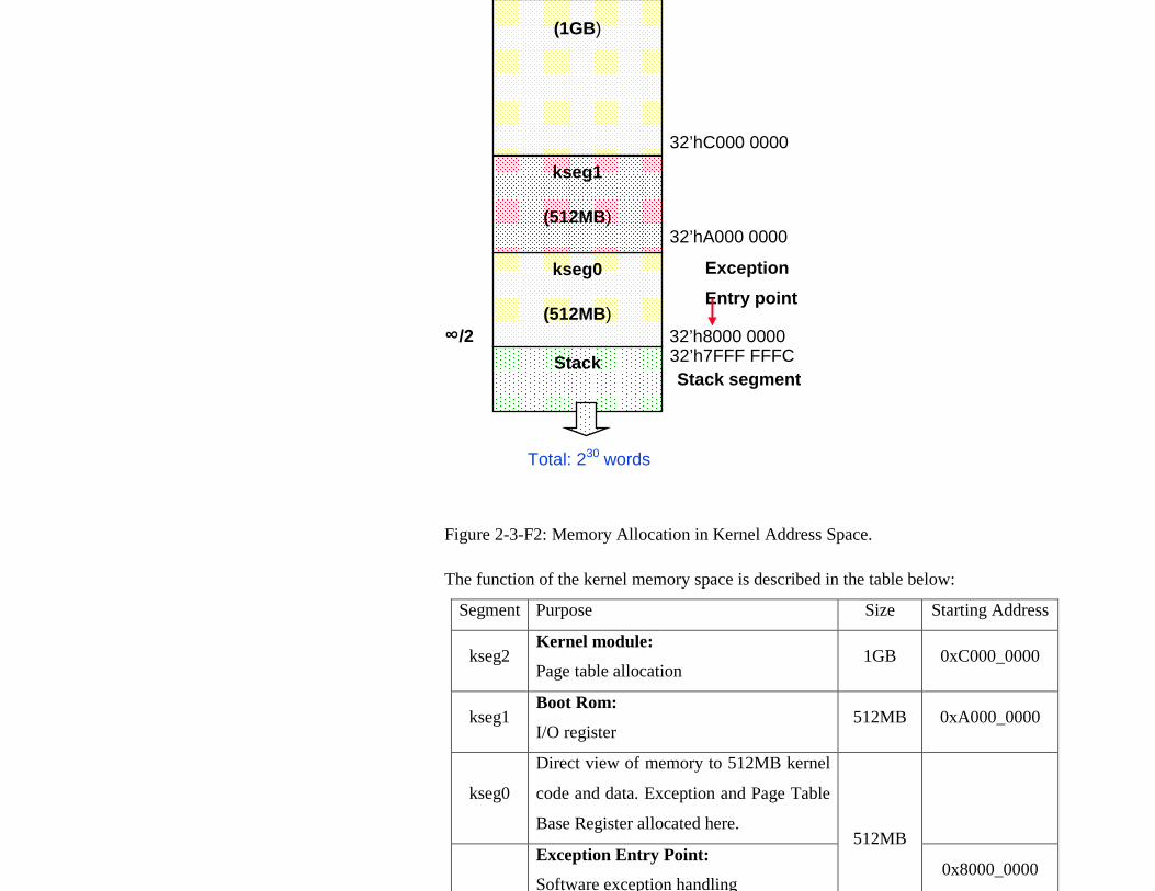
Figure 2-3-F2: Memory Allocation in Kernel Address Space.
The function of the kernel memory space is described in the table below:
Segment Purpose Size Starting Address
kseg2 Kernel module:
Page table allocation 1GB 0xC000_0000
kseg1 Boot Rom:
I/O register 512MB 0xA000_0000
kseg0
Direct view of memory to 512MB kernel
code and data. Exception and Page Table
Base Register allocated here.
Exception Entry Point:
Software exception handling
512MB
0x8000_0000
Stack
kseg0
(512MB)
kseg1
(512MB)
Stack segment
Total: 230 words
32’h7FFF FFFC ∞/2 32’h8000 0000
Exception
Entry point
32’hA000 0000
(1GB)
32’hC000 0000
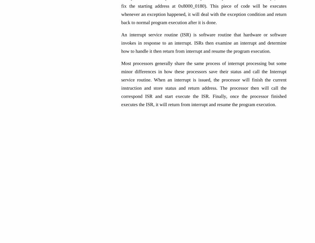
Exception handler is a piece of code that place in a specific address in memory (MIPS
fix the starting address at 0x8000_0180). This piece of code will be executes
whenever an exception happened, it will deal with the exception condition and return
back to normal program execution after it is done.
An interrupt service routine (ISR) is software routine that hardware or software
invokes in response to an interrupt. ISRs then examine an interrupt and determine
how to handle it then return from interrupt and resume the program execution.
Most processors generally share the same process of interrupt processing but some
minor differences in how these processors save their status and call the Interrupt
service routine. When an interrupt is issued, the processor will finish the current
instruction and store status and return address. The processor then will call the
correspond ISR and start execute the ISR. Finally, once the processor finished
executes the ISR, it will return from interrupt and resume the program execution.

Figure 2-4-F1: Interrupt Handling Process.
3-1 Design Specifications
3-1-1 Design Methodology
There are two types of design methodology are available, Top-down design
methodology and Bottom-up design methodology. In top-down design methodology,
the top level representation of a chip is first defined then partitioned into lower level
representations. For bottom-up design methodology, the leaf nodes are first defined.
The leaf nodes are then integrated to form a higher level model of the chip. This
process is repeated until the top level of the chip is reached. Since digital system often
uses the abstraction concepts to simplify the design process, thus top-down design
methodology is used in this project.
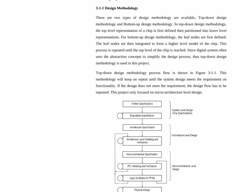
Top-down design methodology process flow is shown in Figure 3-1-1. This
methodology will keep on repeat until the system design meets the requirement on
functionality. If the design does not meet the requirement, the design flow has to be
repeated. This project only focused on micro-architecture level design.
Micro-architecture specification describes the internal design of a unit. The internal
design is described with design-specific technical information for RTL coding to
begin. For this project, the information included for each internal block of UART are:
• UART functionality description
• UART operating procedures
• UART interfaces and I/O pin description
• UART internal operation
• UART functional partitioning into blocks (transmitter, receiver, etc..)
• For each blocks,
o Block interfaces and I/O description
o Block functionality
o Block internal operation
o Finite-state machine (FSM)
o Block test plan
RTL Modeling and Verification
With the micro-architecture specification developed, the RTL coding on UART
internal block can begin. The functional correctness of the model is verified at two
levels:
• Micro-architecture level: Internal blocks of UART are individually verified
before they are integrated into the architecture level.
• Architecture level: The individual blocks of UART are integrated into a unit.
Verification is performed on the UART unit.
After UART unit and all the internal block of UART are verified for functional
correctness, the model is ready for logic synthesis. Logic synthesis is the process of
converting RTL codes into an optimize gate level representation. From the synthesis
result, the gate level netlist is verified for functional correctness. If the specific
requirements are not met, corrections are made either to the gate level netlist or the
RTL models.
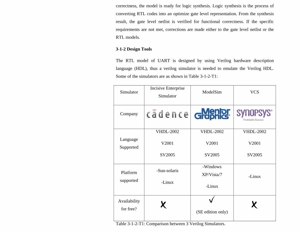
3-1-2 Design Tools
The RTL model of UART is designed by using Verilog hardware description
language (HDL), thus a verilog simulator is needed to emulate the Verilog HDL.
Some of the simulators are as shown in Table 3-1-2-T1:
Simulator Incisive Enterprise
Simulator ModelSim VCS
Company
Language
Supported
VHDL-2002
V2001
SV2005
VHDL-2002
V2001
SV2005
VHDL-2002
V2001
SV2005
Platform
supported
-Sun-solaris
-Linux
-Windows
XP/Vista/7
-Linux
-Linux
Availability
for free?
(SE edition only)
Table 3-1-2-T1: Comparison between 3 Verilog Simulators.

features as well, but the price are too expensive ($25,000 - $100,000) and not
affordable.
As for the synthesis tools, there are a lot of logic synthesis tools that targeting FPGA
e.g. Quartus by Altera, Synplify by Synopsys, ISE by Xilinx, Encounter RTL
Compiler by Cadence Design System, etc. The Xilinx ISE is selected as the synthesis
tools for this project as the Xilinx ISE supports the FPGA that we have in UTAR,
which is Spartan FPGA and both of the tools is already freely available in UTAR.
Mentor Graphics ModelSim PE Student Edition 10.4a
ModelSim from Mentor Graphic is the industry-leading simulation and debugging
environment for HDL (Hardware Description Language) based design which its
license can be obtained for free. Both Verilog and VHDL are supported. This
software provides syntax error checking and waveform simulation. The timing
diagrams and the waveforms can be used to verify the model functionality by writing
a program called a test-bench. Student version instead of full version of the ModelSim
is sufficient for this project.
Xilinx ISE
The ISE development software is designed by Xilinx. This software is designed for
synthesis and analysis of HDL designs, enabling the developer to synthesize their
designs, perform timing analysis, examine RTL diagrams, simulate a design’s
reaction to different stimuli, and configure the target device with the programmer.
Xilinx ISE is a design environment for FPGA products from Xilinx, and cannot be
used with FPGA products from other vendors. The FPGA product that is supported by
Xilinx ISE is Spartan FPGA, Virtex FPGA, Coolrunner and XC9500 Series CPLD.
The FPGA that is going to be used in this project is Spartan FPGA.
FPGA is an integrated circuit designed to be configured by a designer after
manufacturing. The designer can specify the FPGA by using a HDL to configure the
interconnection of the array of programmable logic blocks inside the FPGA. Spartan-
3E FPGA is the logic optimized series. It is ideal for logic integration and for
applications where logic densities matter more than I/O count.
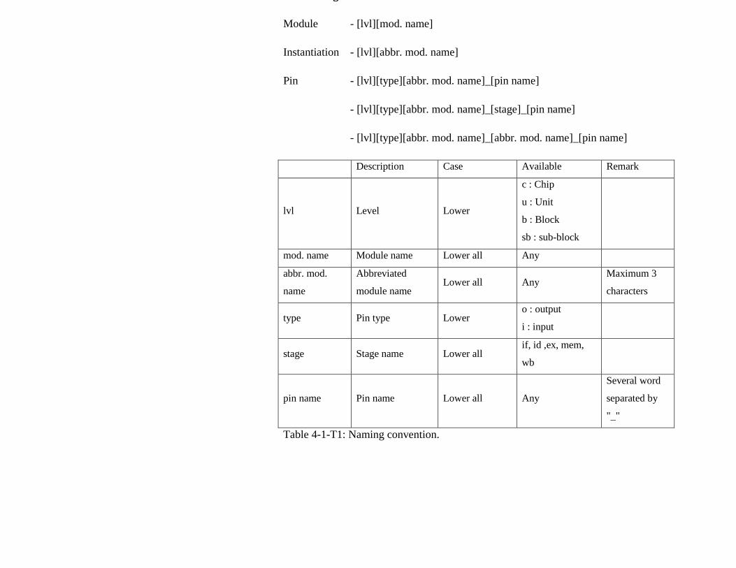
4-1 Naming Convention
Module - [lvl][mod. name]
Instantiation - [lvl][abbr. mod. name]
Pin - [lvl][type][abbr. mod. name]_[pin name]
- [lvl][type][abbr. mod. name]_[stage]_[pin name]
- [lvl][type][abbr. mod. name]_[abbr. mod. name]_[pin name]
Description Case Available Remark
lvl Level Lower
c : Chip
u : Unit
b : Block
sb : sub-block
mod. name Module name Lower all Any
abbr. mod.
name
Abbreviated
module name Lower all Any
Maximum 3
characters
type Pin type Lower o : output
i : input
stage Stage name Lower all if, id ,ex, mem,
wb
pin name Pin name Lower all Any
Several word
separated by
"_"
Table 4-1-T1: Naming convention.

4-2-1 RISC32 Processor Interface
Figure 4-2-1-F1: Block diagram of RISC32 processor.
4-2-2 Input Pin Description
Pin Name:
uirisc_ua_rx_data,
Receive data
Source -> Destination:
DCE -> crisc
Size:
1 bit
Active:
High
Registered:
No
Pin Function:
Serial data to be received from DCE to DTE. When no data is transfer, this port is held at
logic "1".
**DCE - Data Communication Equipment (External Modem)
**DTE - Data Terminal Equipment (UART)
Pin Name:
uirisc_ua_cts,
Clear-To-Send
Source -> Destination:
DCE -> crisc
Size:
1 bit
Active:
High
Registered:
No
Pin Function:
To inform DTE that it can start transmit at uorisc_ua_tx_data port.
Pin Name: Source -> Destination: Size: Active: Registered:
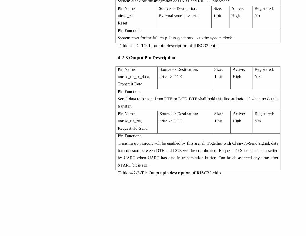
System clock for the integration of UART and RISC32 processor.
Pin Name:
uirisc_rst,
Reset
Source -> Destination:
External source -> crisc
Size:
1 bit
Active:
High
Registered:
No
Pin Function:
System reset for the full chip. It is synchronous to the system clock.
Table 4-2-2-T1: Input pin description of RISC32 chip.
4-2-3 Output Pin Description
Pin Name:
uorisc_ua_tx_data,
Transmit Data
Source -> Destination:
crisc -> DCE
Size:
1 bit
Active:
High
Registered:
Yes
Pin Function:
Serial data to be sent from DTE to DCE. DTE shall hold this line at logic ‘1’ when no data is
transfer.
Pin Name:
uorisc_ua_rts,
Request-To-Send
Source -> Destination:
crisc -> DCE
Size:
1 bit
Active:
High
Registered:
Yes
Pin Function:
Transmission circuit will be enabled by this signal. Together with Clear-To-Send signal, data
transmission between DTE and DCE will be coordinated. Request-To-Send shall be asserted
by UART when UART has data in transmission buffer. Can be de asserted any time after
START bit is sent.
Table 4-2-3-T1: Output pin description of RISC32 chip.

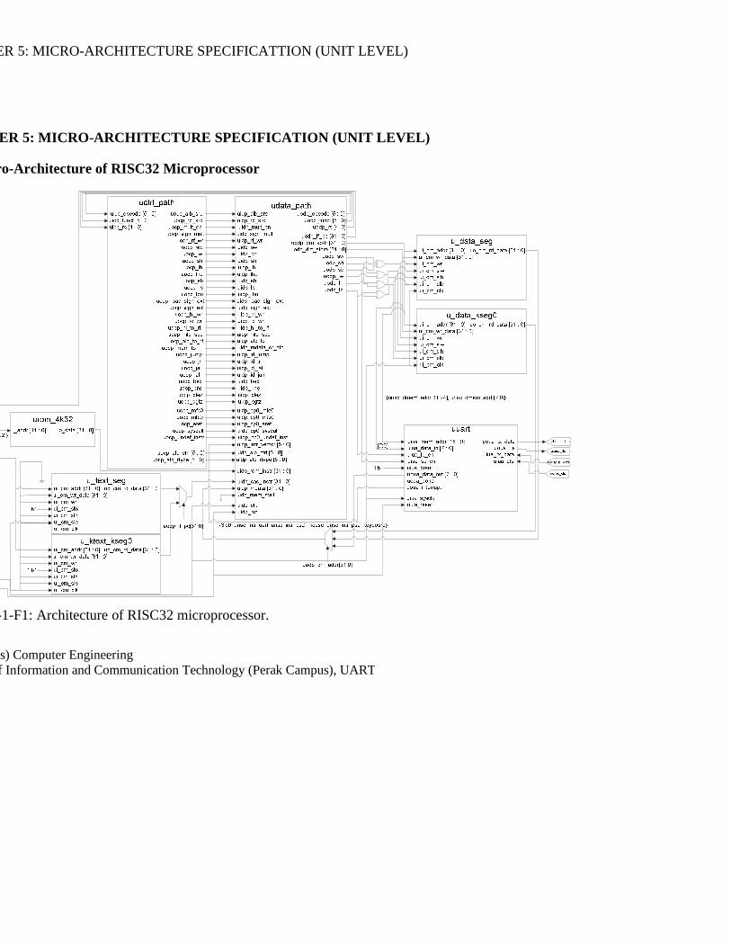
CHAPTER 5: MICRO-ARCHITECTURE SPECIFICATTION (UNIT LEVEL)
BIT (Hons) Computer Engineering Faculty of Information and Communication Technology (Perak Campus), UART
CHAPTER 5: MICRO -ARCHITECTURE SPECIFICATION (UNIT LEVEL)
1 Micro-Architecture of RISC32 Microprocessor
-1-F1: Architecture of RISC32 microprocessor.
CHAPTER 5: MICRO-ARCHITECTURE SPECIFICATTION (UNIT LEVEL)
25 BIT (Hons) Computer Engineering Faculty of Information and Communication Technology (Perak Campus), UART
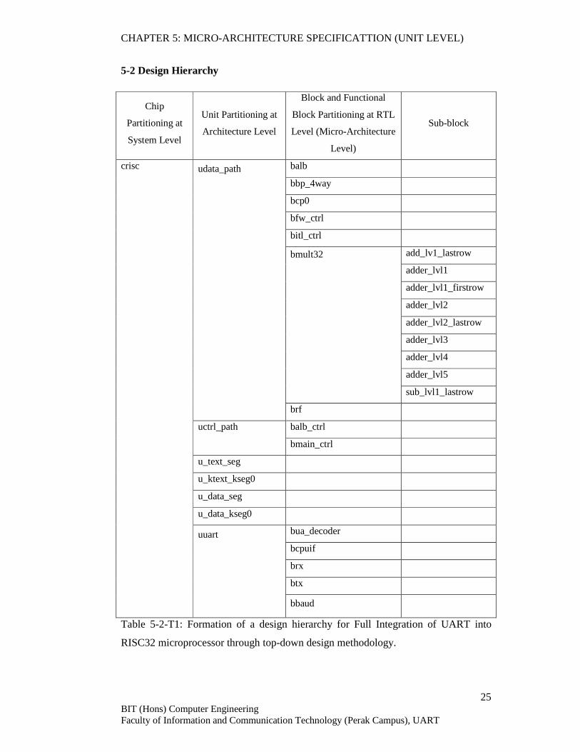
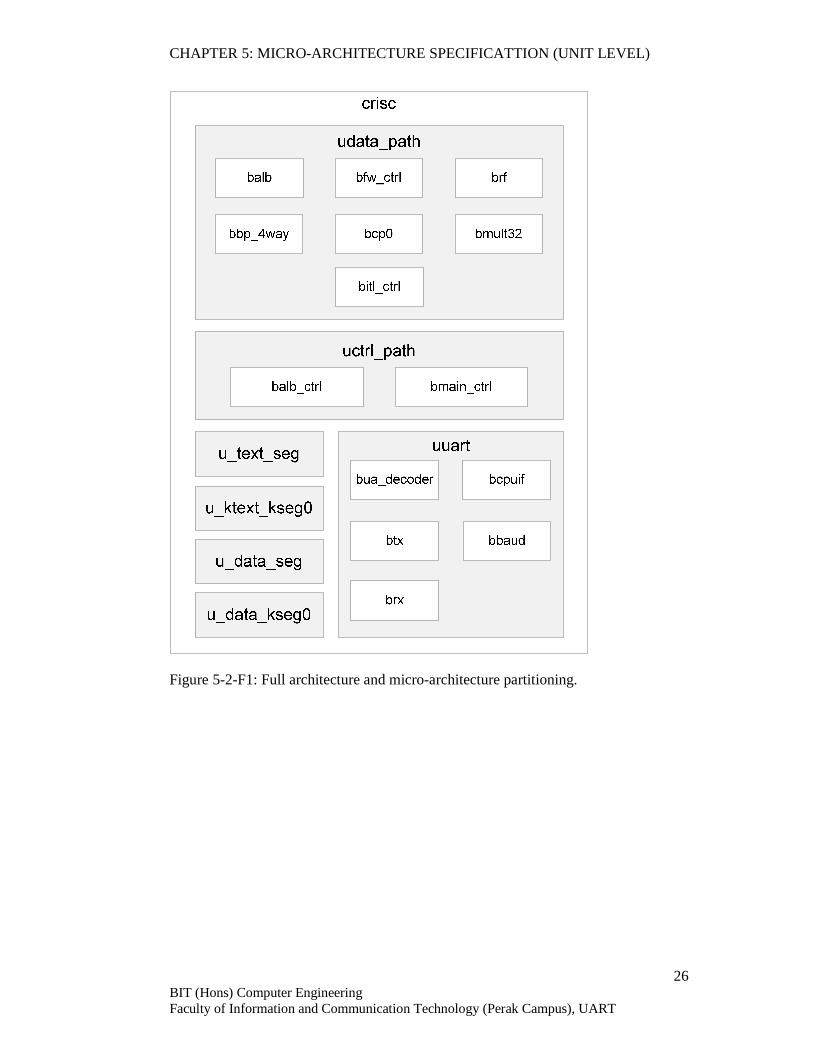
5-2 Design Hierarchy
Chip
Partitioning at
System Level
Unit Partitioning at
Architecture Level
Block and Functional
Block Partitioning at RTL
Level (Micro-Architecture
Level)
Sub-block
balb
bbp_4way
bcp0
bfw_ctrl
bitl_ctrl
add_lv1_lastrow
adder_lvl1
adder_lvl1_firstrow
adder_lvl2
adder_lvl2_lastrow
adder_lvl3
adder_lvl4
adder_lvl5
bmult32
sub_lvl1_lastrow
udata_path
brf
balb_ctrl uctrl_path
bmain_ctrl
u_text_seg
u_ktext_kseg0
u_data_seg
u_data_kseg0
bua_decoder
bcpuif
brx
btx
crisc
uuart
bbaud
Table 5-2-T1: Formation of a design hierarchy for Full Integration of UART into
RISC32 microprocessor through top-down design methodology.
CHAPTER 5: MICRO-ARCHITECTURE SPECIFICATTION (UNIT LEVEL)
26 BIT (Hons) Computer Engineering Faculty of Information and Communication Technology (Perak Campus), UART
Figure 5-2-F1: Full architecture and micro-architecture partitioning.
CHAPTER 5: MICRO-ARCHITECTURE SPECIFICATTION (UNIT LEVEL)
27 BIT (Hons) Computer Engineering Faculty of Information and Communication Technology (Perak Campus), UART
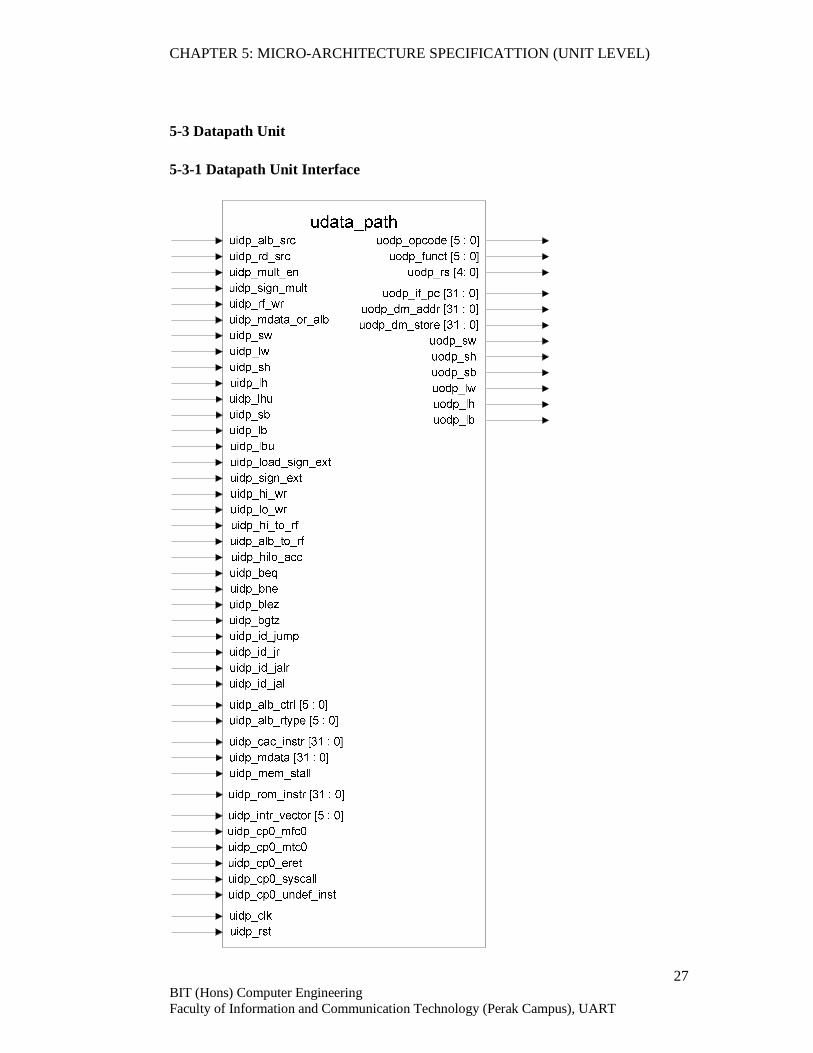
5-3 Datapath Unit
5-3-1 Datapath Unit Interface
CHAPTER 5: MICRO-ARCHITECTURE SPECIFICATTION (UNIT LEVEL)
28 BIT (Hons) Computer Engineering Faculty of Information and Communication Technology (Perak Campus), UART
Figure 5-3-1-F1: Block diagram of RISC32's Datapath Unit.
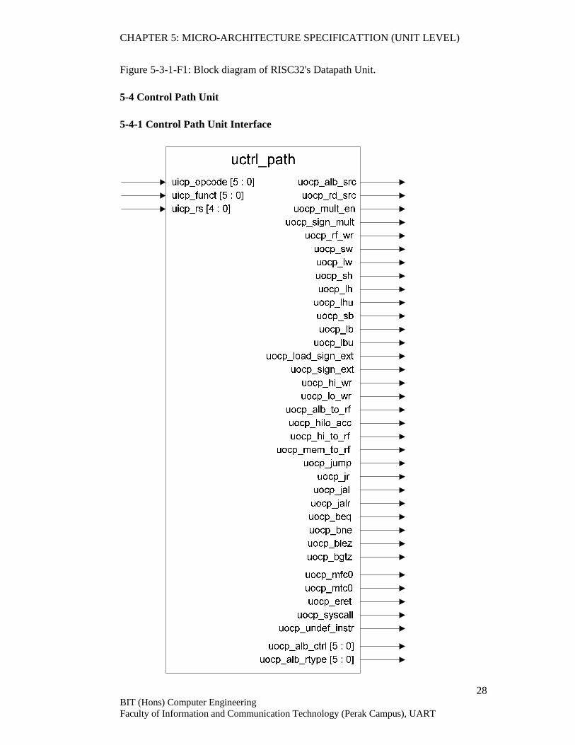
5-4 Control Path Unit
5-4-1 Control Path Unit Interface
CHAPTER 5: MICRO-ARCHITECTURE SPECIFICATTION (UNIT LEVEL)
29 BIT (Hons) Computer Engineering Faculty of Information and Communication Technology (Perak Campus), UART
Figure 5-4-1-F1: Block diagram of RISC32's Control Path Unit.
5-5 Memory Unit
5-5-1 Memory Unit Interface
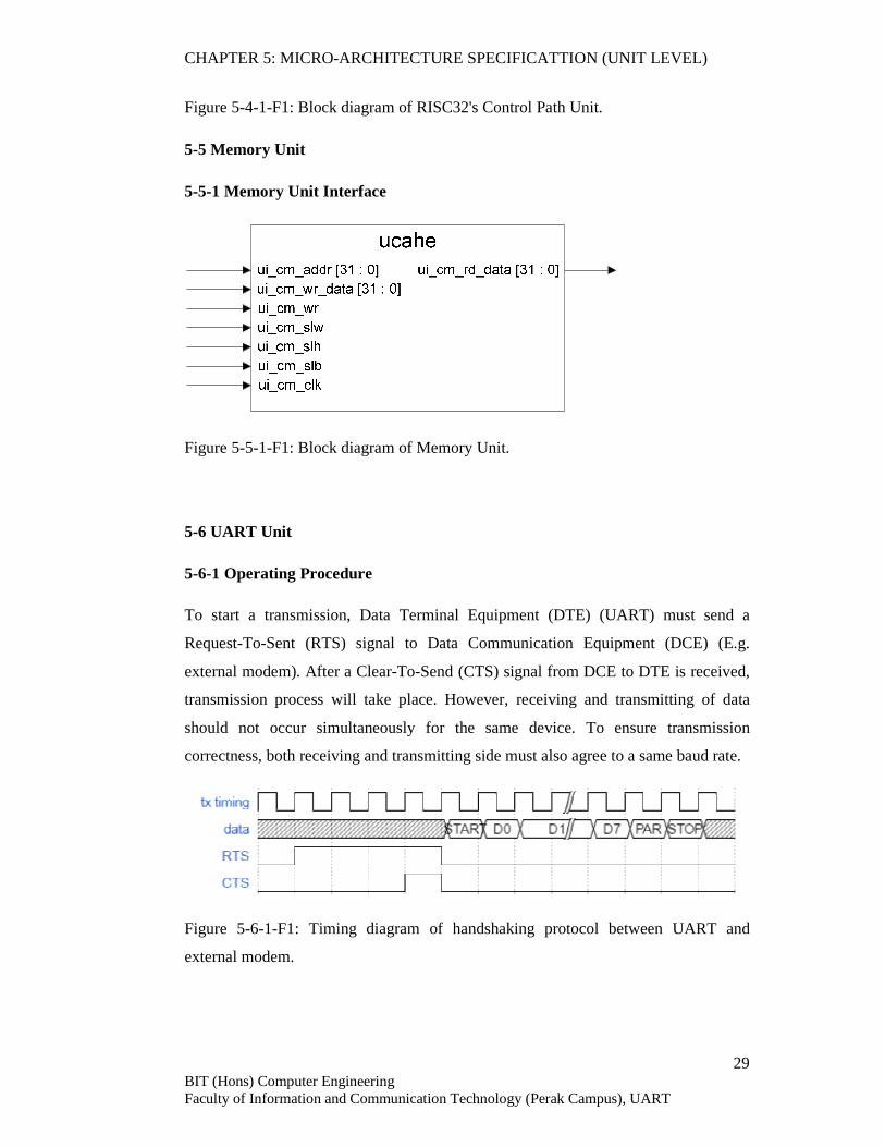
Figure 5-5-1-F1: Block diagram of Memory Unit.
5-6 UART Unit
5-6-1 Operating Procedure
To start a transmission, Data Terminal Equipment (DTE) (UART) must send a
Request-To-Sent (RTS) signal to Data Communication Equipment (DCE) (E.g.
external modem). After a Clear-To-Send (CTS) signal from DCE to DTE is received,
transmission process will take place. However, receiving and transmitting of data
should not occur simultaneously for the same device. To ensure transmission
correctness, both receiving and transmitting side must also agree to a same baud rate.
Figure 5-6-1-F1: Timing diagram of handshaking protocol between UART and
external modem.

CHAPTER 5: MICRO-ARCHITECTURE SPECIFICATTION (UNIT LEVEL)
30 BIT (Hons) Computer Engineering Faculty of Information and Communication Technology (Perak Campus), UART
Figure 5-5-1-F2: UART data transfer protocol.
Figure 5-5-1-F2 shows the data protocol of UART. During transmission, data is
loaded to transmitter block from internal data bus. The data is then used to generate
parity bit. To initiate transmission, start bit ‘0’ is generated and transmitted to DCE.
Followed by 8-bit data and 1 parity bit, shifted out bit by bit. After all the data is
transmitted, a stop bit ‘1’ is transmitted to DCE to indicate the end of transmission.
Figure 5-6-1-F3: Flow chart of UART transmission protocol.

CHAPTER 5: MICRO-ARCHITECTURE SPECIFICATTION (UNIT LEVEL)
31 BIT (Hons) Computer Engineering Faculty of Information and Communication Technology (Perak Campus), UART
Figure 5-6-1-F4: Diagram of UART receive protocol.
The bit stream coming in on rx_data port is not synchronized with the local bit clock.
If we attempt to read rx_data at the rising edge of transmitter clock (baud rate), we
would have a problem is rx_data changed near the clock edge. This could have setup
and hold time problems. If the bit coming in is differed by transmitter clock by a
small amount, we could end up reading some bits at wrong time. To avoid this
problem, the bit coming in from rx_data is sampled at tenth times during each bit time.
Only the middle of the bit will be read for maximum reliability. From Figure 5-5-1-F4,
when the rx_data first goes to '0', it will wait for 5 bclkx10 ticks before it read the start
bit. Then it will wait for another 10 bclkx10 tick to read the first data bit. This will
continue until the stop bit is read.

CHAPTER 5: MICRO-ARCHITECTURE SPECIFICATTION (UNIT LEVEL)
32 BIT (Hons) Computer Engineering Faculty of Information and Communication Technology (Perak Campus), UART
Figure 5-6-1-F5: Flow chart of UART receive protocol.
CHAPTER 5: MICRO-ARCHITECTURE SPECIFICATTION (UNIT LEVEL)
33 BIT (Hons) Computer Engineering Faculty of Information and Communication Technology (Perak Campus), UART
5-6-2 UART Unit Interface
Figure 5-6-2-F1: Block diagram of UART Unit.
5-6-3 Input Pin Description
Pin Name:
uiua_mem_addr,
Memory address
Source -> Destination:
CPU -> uuart
Size:
16 bit
Active:
High
Registered:
No
Pin Function:
Memory address from datapath unit. Used to determine the operation of UART.
Pin Name:
uiua_data_in,
Data input
Source -> Destination:
CPU -> uuart
Size:
8 bit
Active:
High
Registered:
No
Pin Function:
Represent the CPU data to be asserted into UART.
Pin Name:
uiua_lb_en,
Load byte enable
Source -> Destination:
CPU -> UART
Size:
1 bit
Active:
High
Registered:
No
Pin Function:
Use as control signal to read from UART.
Pin Name:
uiua_sb_en,
Store byte enable
Source -> Destination:
CPU -> UART
Size:
1 bit
Active:
High
Registered:
No

CHAPTER 5: MICRO-ARCHITECTURE SPECIFICATTION (UNIT LEVEL)
34 BIT (Hons) Computer Engineering Faculty of Information and Communication Technology (Perak Campus), UART
Pin Function:
Use as control signal to write to UART.
Pin Name:
uiua_grant,
Grant
Source -> Destination:
Arbiter -> UART
Size:
1 bit
Active:
High
Registered:
No
Pin Function:
Use as control signal to read from UART.
Pin Name:
uiua_rx_data
Receive data
Source -> Destination:
DCE -> DTE
Size:
1 bit
Active:
High
Registered:
No
Pin Function:
Serial data to be received from DCE to DTE. When no data is transfer, this port is held at
logic "1".
Pin Name:
uiua_cts
Clear-to-Send
Source -> Destination:
DCE -> DTE
Size:
1 bit
Active:
High
Registered:
No
Pin Function:
To inform UART that it can start transmit at uoua_tx_data port.
Pin Name:
uiua_sysclk,
System Clock
Source -> Destination:
CPU -> UART
Size:
1 bit
Active:
High
Registered:
No
Pin Function:
System clock for all synchronous transfer. The system clock speed is set at 50MHz and it will
be further scale down to 10MHz inside UART.
Pin Name:
uiua_reset,
Reset
Source -> Destination:
CPU -> UART
Size:
1 bit
Active:
High
Registered:
No
Pin Function:
This pin represents the master reset for UART. Once it activate, UART will be at begin state
and in idle mode with no data in UART buffer.
Table 5-6-3-T1: Input pin description of UART unit.
CHAPTER 5: MICRO-ARCHITECTURE SPECIFICATTION (UNIT LEVEL)
35 BIT (Hons) Computer Engineering Faculty of Information and Communication Technology (Perak Campus), UART
5-6-4 Output Pin Description
Pin Name:
uoua_data_out,
Data output
Source -> Destination:
UART -> CPU
Size:
8 bit
Active:
High
Registered:
Yes
Pin Function:
Represent the UART data output to be sent to CPU. The size of the data shall be the same as
the size of Data Input.
Pin Name:
uoua_done,
Done
Source -> Destination:
UART -> Arbiter
Size:
1 bit
Active:
High
Registered:
Yes
Pin Function:
To indicate that UART has complete its operation with CPU after UART acquire the CPU
data bus.
Pin Name:
uoua_interrupt,
Interrupt
Source -> Destination:
UART -> CPU
Size:
1 bit
Active:
High
Registered:
Yes
Pin Function:
An interrupt will be generated when the receiver of UART needs to acquire data bus for their
operation.
Pin Name:
uoua_tx_data,
Transmit data
Source -> Destination:
DTE -> DCE
Size:
1 bit
Active:
High
Registered:
Yes
Pin Function:
Serial data to be sent from DTE to DCE. DTE shall hold this line at logic "1" when no data is
transfer.
Pin Name:
uoua_rts,
Request-to-Sent
Source -> Destination:
DTE -> DCE
Size:
1 bit
Active:
High
Registered:
Yes
Pin Function:
Transmission circuit will be enabled by this signal. Together with Clear-to-Send signal, data
transmission between DTE and DCE will be coordinated, Request-to-Sent shall be asserted by
UART when UART has data in transmission buffer. Can be de-asserted any time after
START bit is sent.
Table 5-6-4-T1: Output pin description of UART unit.
CHAPTER 5: MICRO-ARCHITECTURE SPECIFICATTION (UNIT LEVEL)
36 BIT (Hons) Computer Engineering Faculty of Information and Communication Technology (Perak Campus), UART
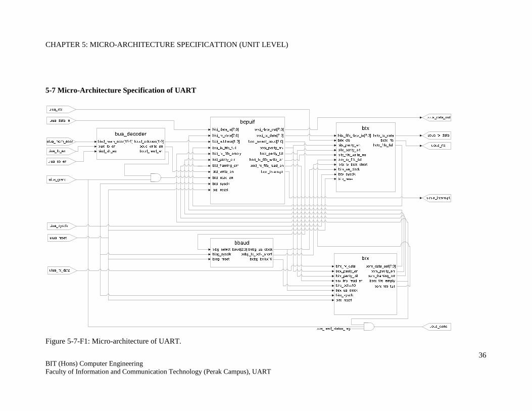
5-7 Micro-Architecture Specification of UART
Figure 5-7-F1: Micro-architecture of UART.
CHAPTER 6: VERIFICATION SPECIFICATION
37 BIT (Hons) Computer Engineering Faculty of Information and Communication Technology (Perak Campus), UART
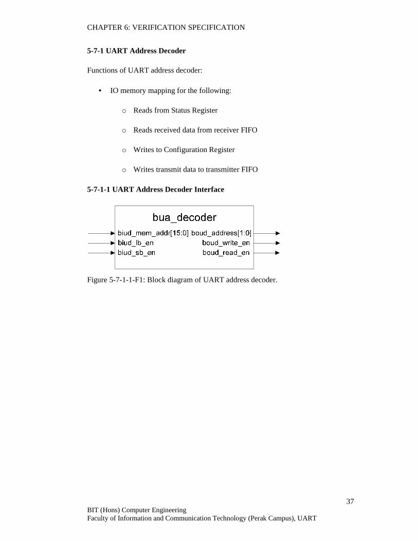
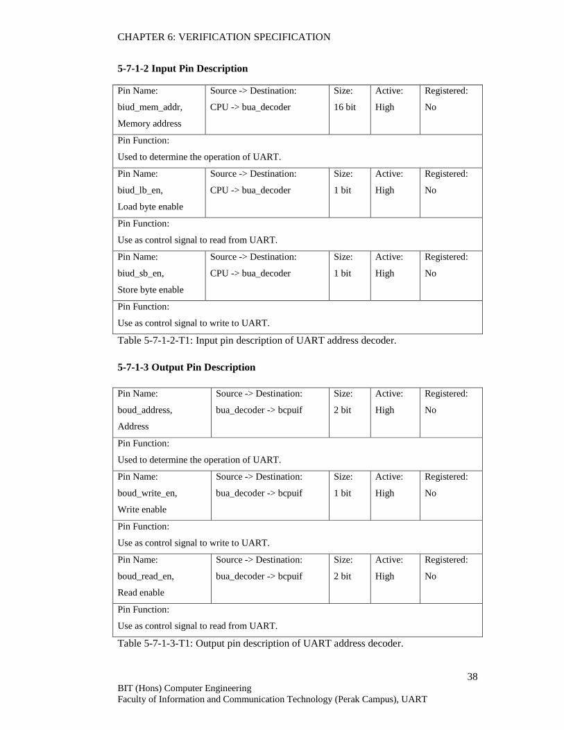
5-7-1 UART Address Decoder
Functions of UART address decoder:
• IO memory mapping for the following:
o Reads from Status Register
o Reads received data from receiver FIFO
o Writes to Configuration Register
o Writes transmit data to transmitter FIFO
5-7-1-1 UART Address Decoder Interface
Figure 5-7-1-1-F1: Block diagram of UART address decoder.
CHAPTER 6: VERIFICATION SPECIFICATION
38 BIT (Hons) Computer Engineering Faculty of Information and Communication Technology (Perak Campus), UART
5-7-1-2 Input Pin Description
Pin Name:
biud_mem_addr,
Memory address
Source -> Destination:
CPU -> bua_decoder
Size:
16 bit
Active:
High
Registered:
No
Pin Function:
Used to determine the operation of UART.
Pin Name:
biud_lb_en,
Load byte enable
Source -> Destination:
CPU -> bua_decoder
Size:
1 bit
Active:
High
Registered:
No
Pin Function:
Use as control signal to read from UART.
Pin Name:
biud_sb_en,
Store byte enable
Source -> Destination:
CPU -> bua_decoder
Size:
1 bit
Active:
High
Registered:
No
Pin Function:
Use as control signal to write to UART.
Table 5-7-1-2-T1: Input pin description of UART address decoder.
5-7-1-3 Output Pin Description
Pin Name:
boud_address,
Address
Source -> Destination:
bua_decoder -> bcpuif
Size:
2 bit
Active:
High
Registered:
No
Pin Function:
Used to determine the operation of UART.
Pin Name:
boud_write_en,
Write enable
Source -> Destination:
bua_decoder -> bcpuif
Size:
1 bit
Active:
High
Registered:
No
Pin Function:
Use as control signal to write to UART.
Pin Name:
boud_read_en,
Read enable
Source -> Destination:
bua_decoder -> bcpuif
Size:
2 bit
Active:
High
Registered:
No
Pin Function:
Use as control signal to read from UART.
Table 5-7-1-3-T1: Output pin description of UART address decoder.
CHAPTER 6: VERIFICATION SPECIFICATION
39 BIT (Hons) Computer Engineering Faculty of Information and Communication Technology (Perak Campus), UART
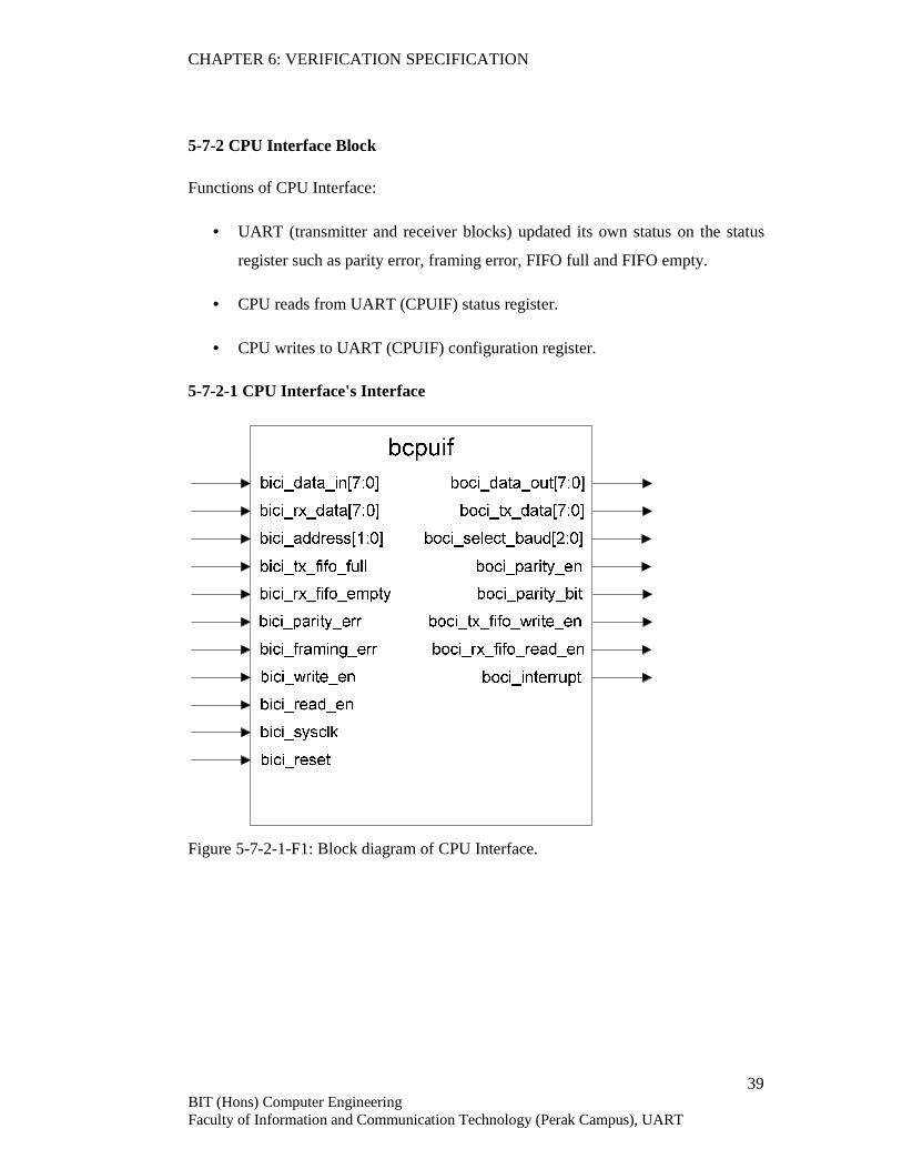
5-7-2 CPU Interface Block
Functions of CPU Interface:
• UART (transmitter and receiver blocks) updated its own status on the status
register such as parity error, framing error, FIFO full and FIFO empty.
• CPU reads from UART (CPUIF) status register.
• CPU writes to UART (CPUIF) configuration register.
5-7-2-1 CPU Interface's Interface
Figure 5-7-2-1-F1: Block diagram of CPU Interface.

CHAPTER 6: VERIFICATION SPECIFICATION
40 BIT (Hons) Computer Engineering Faculty of Information and Communication Technology (Perak Campus), UART
5-7-2-2 Input Pin Description
Pin Name:
bici_data_in,
Data input
Source -> Destination:
CPU -> bcpuif
Size:
8 bit
Active:
High
Registered:
No
Pin Function:
Represent the CPU data to be asserted into UART.
Pin Name:
bici_rx_data,
Received data
Source -> Destination:
brx -> bcpuif
Size:
8 bit
Active:
High
Registered:
No
Pin Function:
Represent the data received from transmitting device and to be asserted to CPU.
Pin Name:
bici_address,
Address
Source -> Destination:
bua_decoder -> bcpuif
Size:
2 bit
Active:
High
Registered:
No
Pin Function:
Represent by 2 bit of CPU address to select which register in the UART to be asserted.
Pin Name:
bici_tx_fifo_full,
Transmitter FIFO full
Source -> Destination:
btx -> bcpuif
Size:
1 bit
Active:
High
Registered:
No
Pin Function:
To indicate transmitter FIFO is full. This signal is to be stored in status register.
Pin Name:
bici_rx_fifo_empty,
Receiver FIFO empty
Source -> Destination:
brx -> bcpuif
Size:
1 bit
Active:
High
Registered:
No
Pin Function:
To indicate receiver FIFO is empty. This signal is to be stored in status register.
Pin Name:
bici_parity_err,
Parity error
Source -> Destination:
brx -> bcpuif
Size:
1 bit
Active:
High
Registered:
No
Pin Function:
Represent parity error of the data. This signal is to be stored in status register.
Pin Name:
bici_framing_err,
Framing error
Source -> Destination:
brx -> bcpuif
Size:
1 bit
Active:
High
Registered:
No
CHAPTER 6: VERIFICATION SPECIFICATION
41 BIT (Hons) Computer Engineering Faculty of Information and Communication Technology (Perak Campus), UART
Pin Function:
Represent framing error of the data. This signal is to be stored in status register.
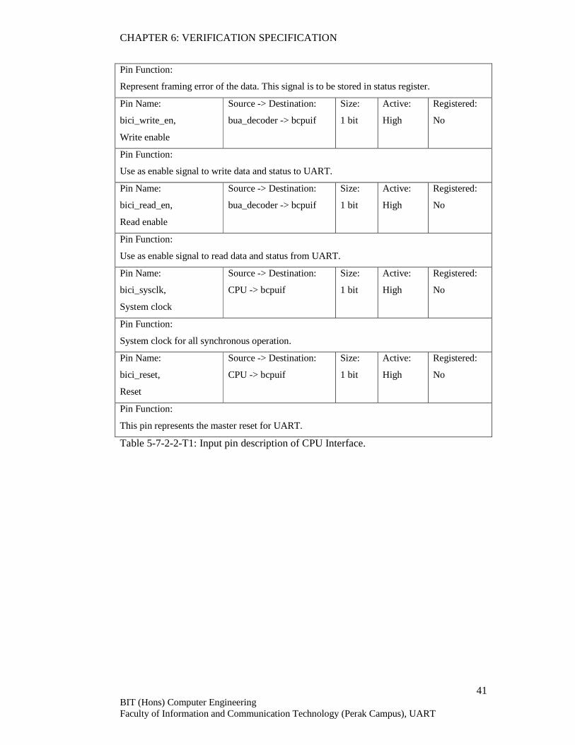
Pin Name:
bici_write_en,
Write enable
Source -> Destination:
bua_decoder -> bcpuif
Size:
1 bit
Active:
High
Registered:
No
Pin Function:
Use as enable signal to write data and status to UART.
Pin Name:
bici_read_en,
Read enable
Source -> Destination:
bua_decoder -> bcpuif
Size:
1 bit
Active:
High
Registered:
No
Pin Function:
Use as enable signal to read data and status from UART.
Pin Name:
bici_sysclk,
System clock
Source -> Destination:
CPU -> bcpuif
Size:
1 bit
Active:
High
Registered:
No
Pin Function:
System clock for all synchronous operation.
Pin Name:
bici_reset,
Reset
Source -> Destination:
CPU -> bcpuif
Size:
1 bit
Active:
High
Registered:
No
Pin Function:
This pin represents the master reset for UART.
Table 5-7-2-2-T1: Input pin description of CPU Interface.
CHAPTER 6: VERIFICATION SPECIFICATION
42 BIT (Hons) Computer Engineering Faculty of Information and Communication Technology (Perak Campus), UART
5-7-2-3 Output Pin Description
Pin Name:
boci_data_out,
Data input
Source -> Destination:
bcpuif -> CPU
Size:
8 bit
Active:
High
Registered:
No
Pin Function:
Represent the UART data output to be sent to CPU. The size of the data shall be the same as
the size of Data In.
Pin Name:
boci_tx_data,
Transmit data
Source -> Destination:
bcpuif -> btx
Size:
8 bit
Active:
High
Registered:
No
Pin Function:
Represent the data to be transmitted to DCE.
Pin Name:
boci_select_baud,
Select baud rate speed
Source -> Destination:
bcpuif -> bbaud
Size:
3 bit
Active:
High
Registered:
No
Pin Function:
To select the baud rate speed for clock controller block. From 000 to 111, there are 8 different
baud rate speeds that can be selected.
Pin Name:
boci_parity_en,
Parity enable
Source -> Destination:
bcpuif -> btx & brx
Size:
1 bit
Active:
High
Registered:
No
Pin Function:
To inform btx and brx whether the data contain a parity bit.
Pin Name:
boci_parity_bit,
Parity bit
Source -> Destination:
bcpuif -> btx & brx
Size:
1 bit
Active:
High
Registered:
No
Pin Function:
To inform btx and brx whether the data is odd or even parity.
Pin Name:
boci_tx_fifo_write_en,
Transmitter FIFO write
enable
Source -> Destination:
bcpuif -> btx
Size:
1 bit
Active:
High
Registered:
No
Pin Function:
An enable signal to write data into transmitter FIFO
CHAPTER 6: VERIFICATION SPECIFICATION
43 BIT (Hons) Computer Engineering Faculty of Information and Communication Technology (Perak Campus), UART
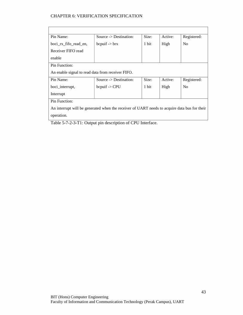
Pin Name:
boci_rx_fifo_read_en,
Receiver FIFO read
enable
Source -> Destination:
bcpuif -> brx
Size:
1 bit
Active:
High
Registered:
No
Pin Function:
An enable signal to read data from receiver FIFO.
Pin Name:
boci_interrupt,
Interrupt
Source -> Destination:
bcpuif -> CPU
Size:
1 bit
Active:
High
Registered:
No
Pin Function:
An interrupt will be generated when the receiver of UART needs to acquire data bus for their
operation.
Table 5-7-2-3-T1: Output pin description of CPU Interface.
CHAPTER 6: VERIFICATION SPECIFICATION
44 BIT (Hons) Computer Engineering Faculty of Information and Communication Technology (Perak Campus), UART
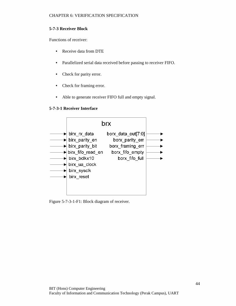
5-7-3 Receiver Block
Functions of receiver:
• Receive data from DTE
• Parallelized serial data received before passing to receiver FIFO.
• Check for parity error.
• Check for framing error.
• Able to generate receiver FIFO full and empty signal.
5-7-3-1 Receiver Interface
Figure 5-7-3-1-F1: Block diagram of receiver.
CHAPTER 6: VERIFICATION SPECIFICATION
45 BIT (Hons) Computer Engineering Faculty of Information and Communication Technology (Perak Campus), UART
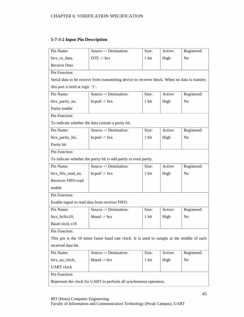
5-7-3-2 Input Pin Description
Pin Name:
birx_rx_data,
Receive Data
Source -> Destination:
DTE -> brx
Size:
1 bit
Active:
High
Registered:
No
Pin Function:
Serial data to be receive from transmitting device to receiver block. When no data is transfer,
this port is held at logic ‘1’.
Pin Name:
birx_parity_en,
Parity enable
Source -> Destination:
bcpuif -> brx
Size:
1 bit
Active:
High
Registered:
No
Pin Function:
To indicate whether the data contain a parity bit.
Pin Name:
birx_parity_bit,
Parity bit
Source -> Destination:
bcpuif -> brx
Size:
1 bit
Active:
High
Registered:
No
Pin Function:
To indicate whether the parity bit is odd parity or even parity.
Pin Name:
birx_fifo_read_en,
Receiver FIFO read
enable
Source -> Destination:
bcpuif -> brx
Size:
1 bit
Active:
High
Registered:
No
Pin Function:
Enable signal to read data from receiver FIFO.
Pin Name:
birx_bclkx10,
Baud clock x10
Source -> Destination:
bbaud -> brx
Size:
1 bit
Active:
High
Registered:
No
Pin Function:
This pin is the 10 times faster baud rate clock. It is used to sample at the middle of each
received data bit.
Pin Name:
birx_ua_clock,
UART clock
Source -> Destination:
bbaud -> brx
Size:
1 bit
Active:
High
Registered:
No
Pin Function:
Represent the clock for UART to perform all synchronous operation.

CHAPTER 6: VERIFICATION SPECIFICATION
46 BIT (Hons) Computer Engineering Faculty of Information and Communication Technology (Perak Campus), UART
Pin Name:
birx_sysclk,
System clock
Source -> Destination:
CPU -> brx
Size:
1 bit
Active:
High
Registered:
No
Pin Function:
System clock for receiver FIFO read operation.
Pin Name:
birx_reset,
Reset
Source -> Destination:
CPU -> brx
Size:
1 bit
Active:
High
Registered:
No
Pin Function:
This pin represents the master reset for UART. Once it activate, brx will be at begin state and
in idle mode.
Table 5-7-3-2-T1: Input pin description of receiver.
5-7-3-3 Output Pin Description
Pin Name:
borx_data_out,
Data output
Source -> Destination:
brx -> bcpuif
Size:
8 bit
Active:
High
Registered:
No
Pin Function:
Represents the parallelized data received from birx_rx_data port. This data is send to bcpuif
and directed to CPU data bus.
Pin Name:
borx_parity_err,
Parity error
Source -> Destination:
brx -> bcpuif
Size:
1 bit
Active:
High
Registered:
No
Pin Function:
Represent parity error of the data.
Pin Name:
borx_framing_err,
Framing error
Source -> Destination:
brx -> bcpuif
Size:
1 bit
Active:
High
Registered:
No
Pin Function:
Represent framing error of the data.
Pin Name:
borx_fifo_empty,
Receiver Fifo Empty
Source -> Destination:
brx -> bcpuif
Size:
1 bit
Active:
High
Registered:
No
Pin Function:
To indicate the receiver FIFO is empty. This signal will pass to bcpuif and store in status

CHAPTER 6: VERIFICATION SPECIFICATION
47 BIT (Hons) Computer Engineering Faculty of Information and Communication Technology (Perak Campus), UART
register.
Pin Name:
borx_fifo_full,
Receiver FIFO Full
Source -> Destination:
brx -> btx
Size:
1 bit
Active:
High
Registered:
No
Pin Function:
To indicate the receiver FIFO is full. This signal will pass to transmitter block. If receiver
FIFO is full, DTE shall not start the transmission to DCE.
Table 5-7-3-3-T1: Output pin description of receiver.
5-7-3-6 Receiver Controller Sub-block
Figure 5-7-3-6-F1: Block diagram of receiver controller sub-block.
5-7-3-7 Input Pin Description of Receiver Controller
Pin Name:
sbirx_rx_data,
Receive Data
Source -> Destination:
DTE -> sbrx_ctr
Size:
1 bit
Active:
High
Registered:
No
Pin Function:
Serial data to be receive from transmitting device to receiver block. When no data is transfer,
this port is held at logic ‘1’.
Pin Name:
sbirx_parity_en,
Parity enable
Source -> Destination:
bcpuif -> sbrx_ctr
Size:
1 bit
Active:
High
Registered:
No
Pin Function:
To indicate whether the data contain a parity bit.
Pin Name:
sbirx_fifo_full,
Receiver FIFO Full
Source -> Destination:
bcpuif -> sbrx_ctr
Size:
1 bit
Active:
High
Registered:
No
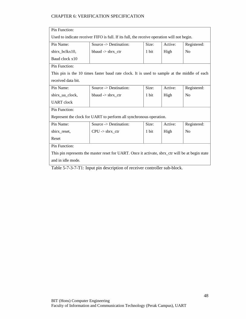
CHAPTER 6: VERIFICATION SPECIFICATION
48 BIT (Hons) Computer Engineering Faculty of Information and Communication Technology (Perak Campus), UART
Pin Function:
Used to indicate receiver FIFO is full. If its full, the receive operation will not begin.
Pin Name:
sbirx_bclkx10,
Baud clock x10
Source -> Destination:
bbaud -> sbrx_ctr
Size:
1 bit
Active:
High
Registered:
No
Pin Function:
This pin is the 10 times faster baud rate clock. It is used to sample at the middle of each
received data bit.
Pin Name:
sbirx_ua_clock,
UART clock
Source -> Destination:
bbaud -> sbrx_ctr
Size:
1 bit
Active:
High
Registered:
No
Pin Function:
Represent the clock for UART to perform all synchronous operation.
Pin Name:
sbirx_reset,
Reset
Source -> Destination:
CPU -> sbrx_ctr
Size:
1 bit
Active:
High
Registered:
No
Pin Function:
This pin represents the master reset for UART. Once it activate, sbrx_ctr will be at begin state
and in idle mode.
Table 5-7-3-7-T1: Input pin description of receiver controller sub-block.

CHAPTER 6: VERIFICATION SPECIFICATION
49 BIT (Hons) Computer Engineering Faculty of Information and Communication Technology (Perak Campus), UART
5-7-3-8 Output Pin Description of Receiver Controller
Pin Name:
sborx_fifo_write_en,
Receiver FIFO write
enable
Source -> Destination:
sbrx_ctr -> brx
Size:
1 bit
Active:
High
Registered:
No
Pin Function:
An enable signal to enable write to receiver FIFO.
Pin Name:
sborx_framing_err,
Framing error
Source -> Destination:
sbrx_ctr -> brx
Size:
1 bit
Active:
High
Registered:
No
Pin Function:
Represent framing error of the data.
Pin Name:
sborx_shift_en,
Shift enable
Source -> Destination:
sbrx_ctr -> brx
Size:
1 bit
Active:
High
Registered:
No
Pin Function:
Enable signal for shift register in brx to sample data.
Table 5-7-3-8-T1: Output pin description of receiver controller sub-block.
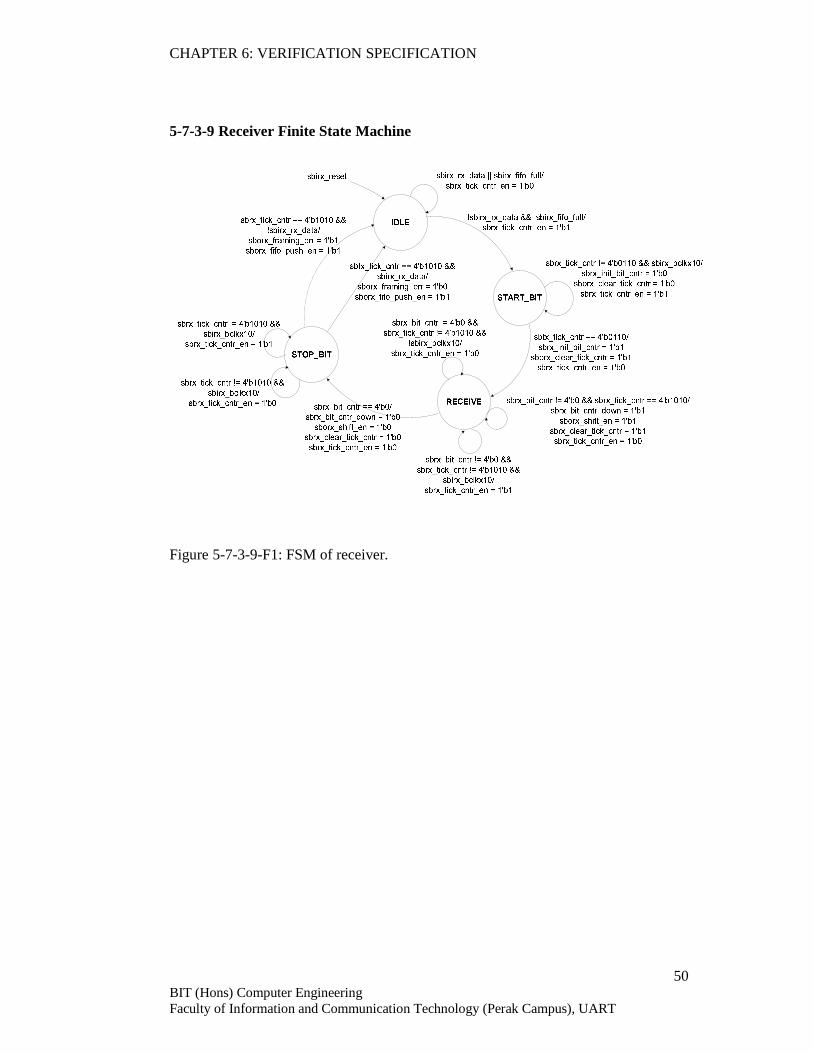
CHAPTER 6: VERIFICATION SPECIFICATION
50 BIT (Hons) Computer Engineering Faculty of Information and Communication Technology (Perak Campus), UART
5-7-3-9 Receiver Finite State Machine
Figure 5-7-3-9-F1: FSM of receiver.
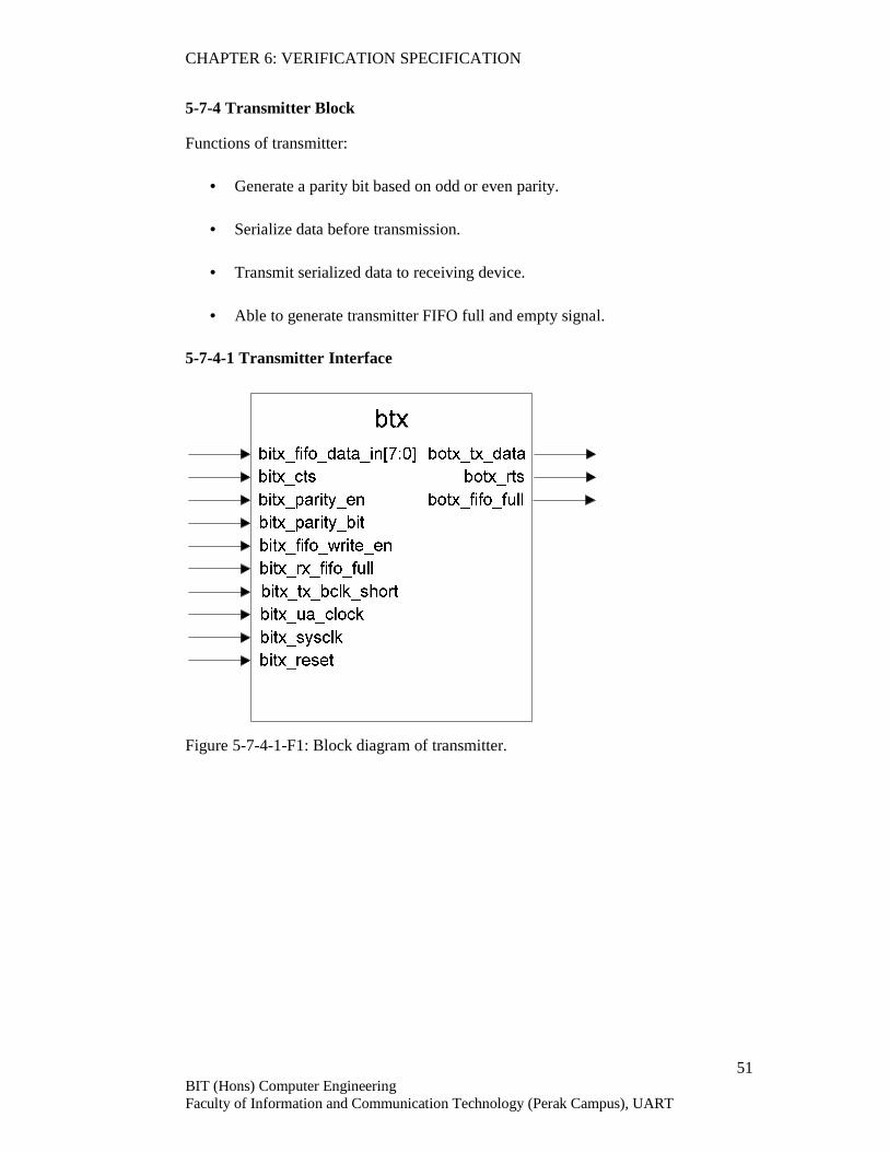
CHAPTER 6: VERIFICATION SPECIFICATION
51 BIT (Hons) Computer Engineering Faculty of Information and Communication Technology (Perak Campus), UART
5-7-4 Transmitter Block
Functions of transmitter:
• Generate a parity bit based on odd or even parity.
• Serialize data before transmission.
• Transmit serialized data to receiving device.
• Able to generate transmitter FIFO full and empty signal.
5-7-4-1 Transmitter Interface
Figure 5-7-4-1-F1: Block diagram of transmitter.
CHAPTER 6: VERIFICATION SPECIFICATION
52 BIT (Hons) Computer Engineering Faculty of Information and Communication Technology (Perak Campus), UART
5-7-4-2 Input Pin Description
Pin Name:
bitx_fifo_data_in,
FIFO data input
Source -> Destination:
bcpuif -> btx
Size:
8 bit
Active:
High
Registered:
No
Pin Function:
Represent the data to be transmitted to receiving device. This data will store to transmitter
FIFO first before it’s transmit at botx_tx_data port.
Pin Name:
bitx_cts,
Clear-To-Send
Source -> Destination:
DCE -> btx
Size:
1 bit
Active:
High
Registered:
No
Pin Function:
To inform DTE that it can start to transmit data on botx_tx_data port.
Pin Name:
bitx_parity_en,
Parity enable
Source -> Destination:
bcpuif -> btx
Size:
1 bit
Active:
High
Registered:
No
Pin Function:
To indicate whether the data contain a parity bit.
Pin Name:
bitx_parity_bit,
Parity bit
Source -> Destination:
bcpuif -> btx
Size:
1 bit
Active:
High
Registered:
No
Pin Function:
To indicate whether the parity bit is odd parity or even parity.
Pin Name:
bitx_fifo_write_en,
Transmitter FIFO write
enable
Source -> Destination:
bcpuif -> btx
Size:
1 bit
Active:
High
Registered:
No
Pin Function:
Enable signal to write to transmitter FIFO.
Pin Name:
bitx_rx_fifo_full,
Receiver FIFO full
Source -> Destination:
brx -> btx
Size:
1 bit
Active:
High
Registered:
No
Pin Function:
To indicate whether the receiver FIFO is full. If it is not full, transmitter will reply a CTS
signal to DTE.

CHAPTER 6: VERIFICATION SPECIFICATION
53 BIT (Hons) Computer Engineering Faculty of Information and Communication Technology (Perak Campus), UART
Pin Name:
bitx_tx_bclk_short,
Transmitter baud clock
short
Source -> Destination:
bbaud -> btx
Size:
1 bit
Active:
High
Registered:
No
Pin Function:
This is the one-cycle-tick signal to enable the serial transmission on botx_tx_data port.
Pin Name:
bitx_ua_clock,
UART clock
Source -> Destination:
bbaud -> btx
Size:
1 bit
Active:
High
Registered:
No
Pin Function:
Represent the clock for UART to perform all synchronous operation.
Pin Name:
bitx_sysclk,
System clock
Source -> Destination:
CPU -> btx
Size:
1 bit
Active:
High
Registered:
No
Pin Function:
System clock for transmitter FIFO write operation.
Pin Name:
bitx_reset,
Reset
Source -> Destination:
CPU ->btx
Size:
1 bit
Active:
High
Registered:
No
Pin Function:
This pin represents the master reset for UART. Once it activate, btx will be at begin state and
in idle mode.
Table 5-7-4-2-T1: Input pin description of transmitter.
CHAPTER 6: VERIFICATION SPECIFICATION
54 BIT (Hons) Computer Engineering Faculty of Information and Communication Technology (Perak Campus), UART
5-7-4-3 Output Pin Description
Pin Name:
botx_tx_data,
Transmit data
Source -> Destination:
btx -> DCE
Size:
1 bit
Active:
High
Registered:
No
Pin Function:
Serial data to be sent from DTE to DCE. DTE shall hold this line at logic ‘1’ when no data is
transfer.
Pin Name:
botx_rts,
Request-To-Send
Source -> Destination:
btx -> DCE
Size:
1 bit
Active:
High
Registered:
No
Pin Function:
Transmission circuit will be enabled by this signal. Together with Clear-To-Send signal, data
transmission between DTE and DCE will be coordinated. Request-To-Send shall be asserted
whenever there is data in transmitter FIFO. Can be de asserted any time after START bit is
sent.
Pin Name:
botx_fifo_full,
Transmitter FIFO Full
Source -> Destination:
btx -> bcpuif
Size:
1 bit
Active:
High
Registered:
No
Pin Function:
To indicate whether the transmitter FIFO is full. This signal pass to bcpuif and store inside
status register.
Table 5-7-4-3-T1: Output pin description of transmitter.

CHAPTER 6: VERIFICATION SPECIFICATION
55 BIT (Hons) Computer Engineering Faculty of Information and Communication Technology (Perak Campus), UART
5-7-4-6 Transmitter Controller Sub-block
Figure 5-7-4-6-F1: Block diagram of transmitter controller sub-block.
5-7-4-7 Input Pin Description of Transmitter Controller
Pin Name:
sbitx_cts,
Clear-To-Send
Source -> Destination:
DCE -> sbtx_ctr
Size:
1 bit
Active:
High
Registered:
No
Pin Function:
To inform DTE that it can start to transmit data on botx_tx_data.
Pin Name:
sbitx_parity_en,
Parity enable
Source -> Destination:
bcpuif -> sbtx_ctr
Size:
1 bit
Active:
High
Registered:
No
Pin Function:
To indicate whether the data contain a parity bit.
Pin Name:
sbitx_tx_fifo_empty,
Transmitter FIFO empty
Source -> Destination:
btx -> sbtx_ctr
Size:
1 bit
Active:
High
Registered:
No
Pin Function:
To indicate whether transmitter FIFO is empty. If it is not empty, transmitter will read the
data and begin the transmit operation.
Pin Name:
sbitx_rx_fifo_full,
Receiver FIFO full
Source -> Destination:
brx -> sbtx_ctr
Size:
1 bit
Active:
High
Registered:
No
Pin Function:
To indicate whether the receiver FIFO is full. If it is not full, transmitter will reply a CTS
signal to DTE.
CHAPTER 6: VERIFICATION SPECIFICATION
56 BIT (Hons) Computer Engineering Faculty of Information and Communication Technology (Perak Campus), UART
Pin Name:
sbitx_tx_bclk_short,
Transmitter enable
Source -> Destination:
bbaud -> sbtx_ctr
Size:
1 bit
Active:
High
Registered:
No
Pin Function:
Enable signal to transmit serial data on botx_tx_data port.
Pin Name:
sbitx_ua_clock,
UART clock
Source -> Destination:
bbaud -> sbtx_ctr
Size:
1 bit
Active:
High
Registered:
No
Pin Function:
Represent the clock for UART to perform all synchronous operation.
Pin Name:
sbitx_reset,
Reset
Source -> Destination:
CPU -> sbtx_ctr
Size:
1 bit
Active:
High
Registered:
No
Pin Function:
This pin represents the master reset for UART. Once it activate, sbtx_ctr will be at begin state
and in idle mode.
Table 5-7-4-7-T1: Input pin description of transmitter controller sub-block.
5-7-4-8 Output Pin Description of Transmitter Controller
Pin Name:
sbotx_rts,
Request-To-Send
Source -> Destination:
sbtx_ctr -> DCE
Size:
1 bit
Active:
High
Registered:
No
Pin Function:
Transmission circuit will be enabled by this signal. Together with Clear-To-Send signal, data
transmission between DTE and DCE will be coordinated. Request-To-Send shall be asserted
whenever there is data in transmitter FIFO. Can be de asserted any time after START bit is
sent.
Pin Name:
sbotx_fifo_read_en,
Receiver FIFO read
enable
Source -> Destination:
sbtx_ctr -> btx
Size:
1 bit
Active:
High
Registered:
No
Pin Function:
Enable signal to read from transmitter FIFO.
Pin Name:
sbotx_shift_en,
Shift enable
Source -> Destination:
sbtx_ctr -> btx
Size:
1 bit
Active:
High
Registered:
No
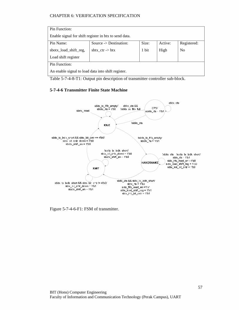
CHAPTER 6: VERIFICATION SPECIFICATION
57 BIT (Hons) Computer Engineering Faculty of Information and Communication Technology (Perak Campus), UART
Pin Function:
Enable signal for shift register in btx to send data.
Pin Name:
sbotx_load_shift_reg,
Load shift register
Source -> Destination:
sbtx_ctr -> btx
Size:
1 bit
Active:
High
Registered:
No
Pin Function:
An enable signal to load data into shift register.
Table 5-7-4-8-T1: Output pin description of transmitter controller sub-block.
5-7-4-6 Transmitter Finite State Machine
Figure 5-7-4-6-F1: FSM of transmitter.
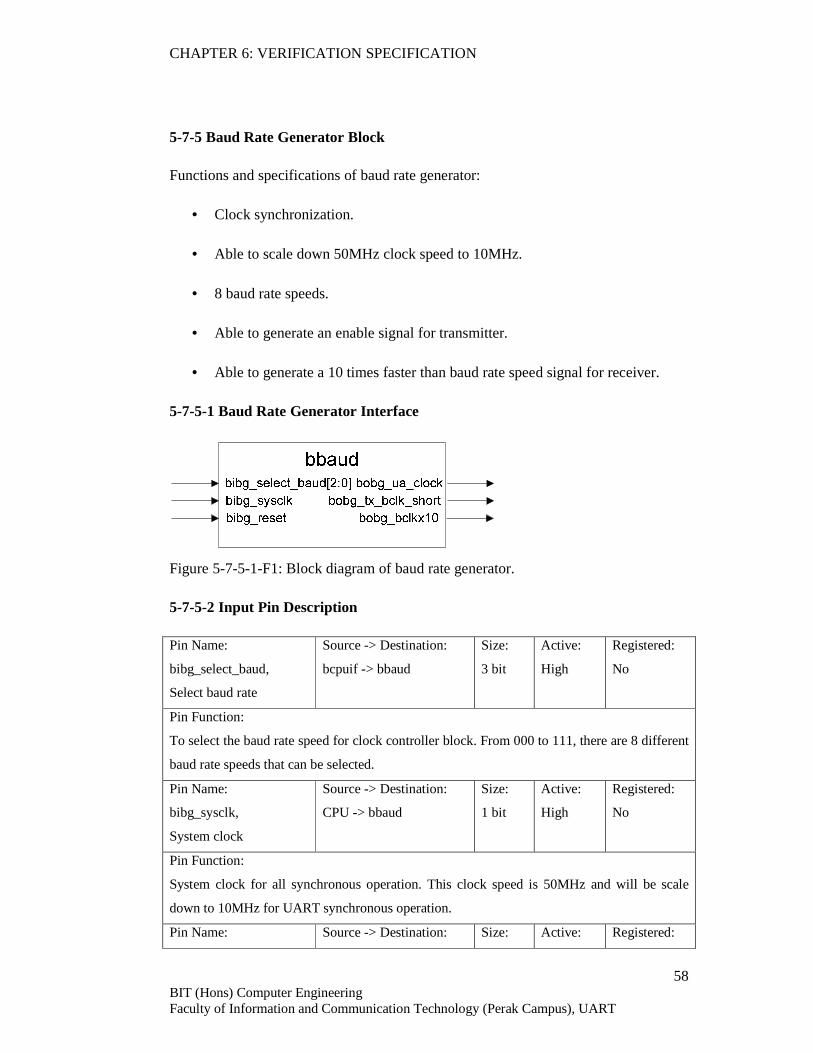
CHAPTER 6: VERIFICATION SPECIFICATION
58 BIT (Hons) Computer Engineering Faculty of Information and Communication Technology (Perak Campus), UART
5-7-5 Baud Rate Generator Block
Functions and specifications of baud rate generator:
• Clock synchronization.
• Able to scale down 50MHz clock speed to 10MHz.
• 8 baud rate speeds.
• Able to generate an enable signal for transmitter.
• Able to generate a 10 times faster than baud rate speed signal for receiver.
5-7-5-1 Baud Rate Generator Interface
Figure 5-7-5-1-F1: Block diagram of baud rate generator.
5-7-5-2 Input Pin Description
Pin Name:
bibg_select_baud,
Select baud rate
Source -> Destination:
bcpuif -> bbaud
Size:
3 bit
Active:
High
Registered:
No
Pin Function:
To select the baud rate speed for clock controller block. From 000 to 111, there are 8 different
baud rate speeds that can be selected.
Pin Name:
bibg_sysclk,
System clock
Source -> Destination:
CPU -> bbaud
Size:
1 bit
Active:
High
Registered:
No
Pin Function:
System clock for all synchronous operation. This clock speed is 50MHz and will be scale
down to 10MHz for UART synchronous operation.
Pin Name: Source -> Destination: Size: Active: Registered:
CHAPTER 6: VERIFICATION SPECIFICATION
59 BIT (Hons) Computer Engineering Faculty of Information and Communication Technology (Perak Campus), UART
bibg_reset,
Reset
CPU -> bbaud 1 bit High No
Pin Function:
This pin represents the master reset for UART. Once it activate, all the outputs of bbaud will
be reset to initial state.
Table 5-7-5-2-T1: Input pin description of baud rate generator.
5-7-5-3 Output Pin Description
Pin Name:
bobg_ua_clock,
UART clock
Source -> Destination:
bbaud -> btx
Size:
1 bit
Active:
High
Registered:
No
Pin Function:
10MHz clock signal for all the UART synchronous operation.
Pin Name:
bobg_tx_bclk_short,
Transmit baud clock
short
Source -> Destination:
bbaud -> btx
Size:
1 bit
Active:
High
Registered:
No
Pin Function:
Enable signal for transmitter to transmit data.
Pin Name:
bobg_bclkx10,
Baud clock x10
Source -> Destination:
bbaud -> brx
Size:
1 bit
Active:
High
Registered:
No
Pin Function:
This pin is the 10 times faster baud rate clock. It is used by receiver to sample at the middle of
each received data bit.
Table 5-7-5-3-T1: Output pin description of baud rate generator.

CHAPTER 6: VERIFICATION SPECIFICATION
60 BIT (Hons) Computer Engineering Faculty of Information and Communication Technology (Perak Campus), UART
CHAPTER 6: VERIFICATION SPECIFICATION
6-1 UART Test
6-1-1 Test Plan of UART
Test Function to be Tested
Expected Output
Test Case #1: Reset • Set the reset pin to high. • Hold for 10 clock cycle. • Set the reset pin to low.
Reset the whole UART unit.
uoua_data_out = 8’b0 uoua_rts = 1’b0 uoua_tx_data = 1’b1
Test Case #2: Send data with Odd Parity • Assert the enable parity bit in
configuration register. • Assert the parity bit in configuration
register. • Send transmit data to UART,
uiua_data_in = 8’b10101010. • Set uiua_cts to high.
• Hold for 1 clock cycle. • Set uiua_cts to low.
Transmit a data with Odd Parity.
uoua_tx_data = 11 1010_1010 0 * Parity bit (Bit 10 of transmit data) = 1
Test Case #3: Send data with Even Parity • Assert the enable parity bit in
configuration register. • De-assert the parity bit in configuration
register. • Send transmit data to UART,
uiua_data_in = 8’b11110000. • Set uiua_cts to high. • Hold for 1 clock cycle. • Set uiua_cts to low.
Transmit a data with Even Parity.
uoua_tx_data = 10 1111_0000 0 *Parity bit (Bit 10 of transmit data) = 0
Test Case #4: Send data with no parity • De-assert the enable parity bit in
configuration register.
• Send transmit data to UART, uiua_data_in = 8’b11001100.
• Set uiua_cts to high. • Hold for 1 clock cycle. • Set uiua_cts to low.
Transmit a data with no parity
uoua_tx_data = 1 1100_1100 0 *No parity is transmitted
Test Case #5: Receive data with Odd Parity • Assert the enable parity bit in
configuration register. • Assert the parity bit in configuration
register. • Transmit 11_0100_0100_0 bit by bit to
Receive an odd parity data from external side. Interrupt signal will be generated. The data and
uoua_interrupt = 1’b1 uoua_data_out = 8’b01000100 uoua_data_out = 8’b00000010
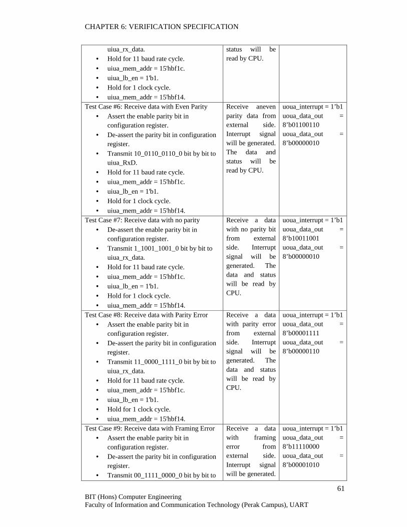
CHAPTER 6: VERIFICATION SPECIFICATION
61 BIT (Hons) Computer Engineering Faculty of Information and Communication Technology (Perak Campus), UART
uiua_rx_data. • Hold for 11 baud rate cycle.
• uiua_mem_addr = 15'hbf1c. • uiua_lb_en = 1'b1. • Hold for 1 clock cycle. • uiua_mem_addr = 15'hbf14.
status will be read by CPU.
Test Case #6: Receive data with Even Parity • Assert the enable parity bit in
configuration register. • De-assert the parity bit in configuration
register. • Transmit 10_0110_0110_0 bit by bit to
uiua_RxD. • Hold for 11 baud rate cycle. • uiua_mem_addr = 15'hbf1c. • uiua_lb_en = 1'b1. • Hold for 1 clock cycle.
• uiua_mem_addr = 15'hbf14.
Receive aneven parity data from external side. Interrupt signal will be generated. The data and status will be read by CPU.
uoua_interrupt = 1’b1 uoua_data_out = 8’b01100110 uoua_data_out = 8’b00000010
Test Case #7: Receive data with no parity • De-assert the enable parity bit in
configuration register. • Transmit 1_1001_1001_0 bit by bit to
uiua_rx_data. • Hold for 11 baud rate cycle. • uiua_mem_addr = 15'hbf1c. • uiua_lb_en = 1'b1. • Hold for 1 clock cycle. • uiua_mem_addr = 15'hbf14.
Receive a data with no parity bit from external side. Interrupt signal will be generated. The data and status will be read by CPU.
uoua_interrupt = 1’b1 uoua_data_out = 8’b10011001 uoua_data_out = 8’b00000010
Test Case #8: Receive data with Parity Error • Assert the enable parity bit in
configuration register. • De-assert the parity bit in configuration
register. • Transmit 11_0000_1111_0 bit by bit to
uiua_rx_data. • Hold for 11 baud rate cycle. • uiua_mem_addr = 15'hbf1c.
• uiua_lb_en = 1'b1. • Hold for 1 clock cycle. • uiua_mem_addr = 15'hbf14.
Receive a data with parity error from external side. Interrupt signal will be generated. The data and status will be read by CPU.
uoua_interrupt = 1’b1 uoua_data_out = 8’b00001111 uoua_data_out = 8’b00000110
Test Case #9: Receive data with Framing Error • Assert the enable parity bit in
configuration register. • De-assert the parity bit in configuration
register. • Transmit 00_1111_0000_0 bit by bit to
Receive a data with framing error from external side. Interrupt signal will be generated.
uoua_interrupt = 1’b1 uoua_data_out = 8’b11110000 uoua_data_out = 8’b00001010
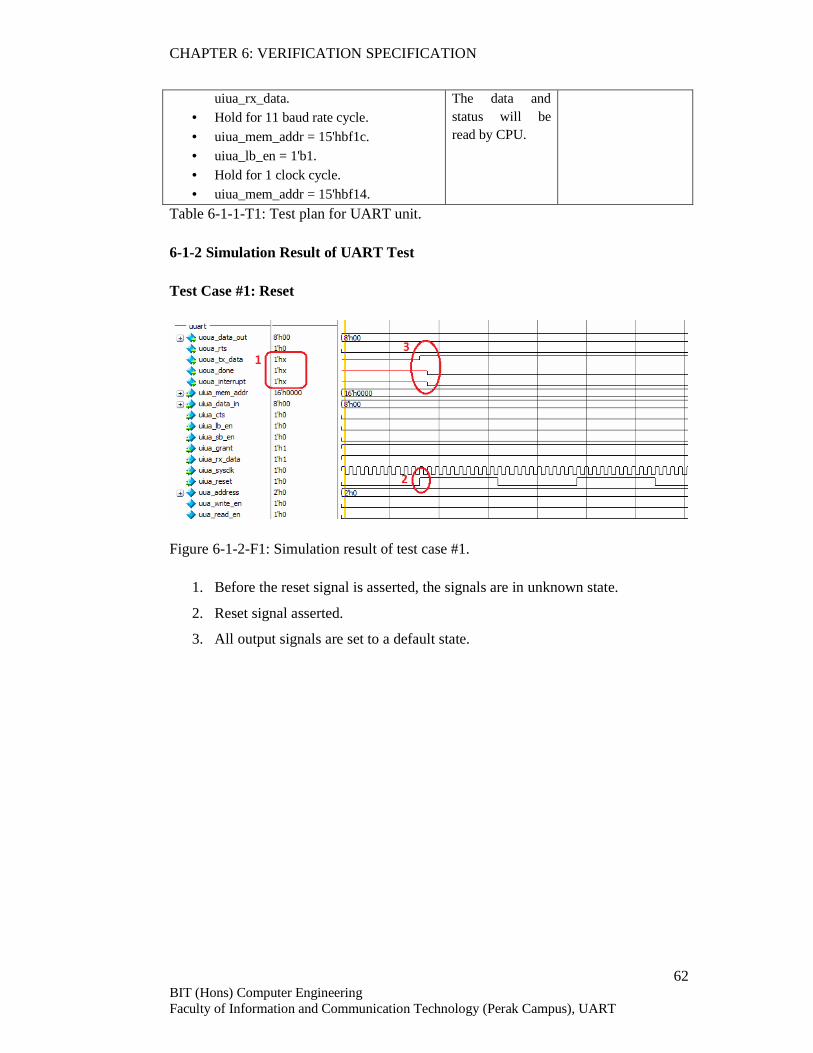
CHAPTER 6: VERIFICATION SPECIFICATION
62 BIT (Hons) Computer Engineering Faculty of Information and Communication Technology (Perak Campus), UART
uiua_rx_data. • Hold for 11 baud rate cycle.
• uiua_mem_addr = 15'hbf1c. • uiua_lb_en = 1'b1. • Hold for 1 clock cycle. • uiua_mem_addr = 15'hbf14.
The data and status will be read by CPU.
Table 6-1-1-T1: Test plan for UART unit.
6-1-2 Simulation Result of UART Test
Test Case #1: Reset
Figure 6-1-2-F1: Simulation result of test case #1.
1. Before the reset signal is asserted, the signals are in unknown state.
2. Reset signal asserted.
3. All output signals are set to a default state.
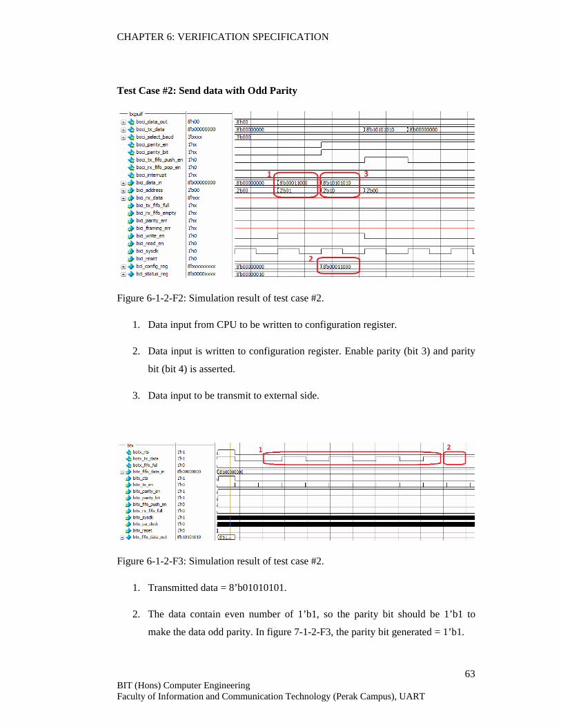
CHAPTER 6: VERIFICATION SPECIFICATION
63 BIT (Hons) Computer Engineering Faculty of Information and Communication Technology (Perak Campus), UART
Test Case #2: Send data with Odd Parity
Figure 6-1-2-F2: Simulation result of test case #2.
1. Data input from CPU to be written to configuration register.
2. Data input is written to configuration register. Enable parity (bit 3) and parity
bit (bit 4) is asserted.
3. Data input to be transmit to external side.
Figure 6-1-2-F3: Simulation result of test case #2.
1. Transmitted data = 8’b01010101.
2. The data contain even number of 1’b1, so the parity bit should be 1’b1 to
make the data odd parity. In figure 7-1-2-F3, the parity bit generated = 1’b1.

CHAPTER 6: VERIFICATION SPECIFICATION
64 BIT (Hons) Computer Engineering Faculty of Information and Communication Technology (Perak Campus), UART
Test Case #3: Send data with Even Parity
Figure 6-1-2-F4: Simulation result of test case #3.
1. Data input to be written to configuration register.
2. Data input is written to configuration register. Enable parity (bit 3) is asserted
and parity bit (bit 4) is de-asserted.
3. Data input to be transmit to external side.
Figure 6-1-2-F5: Simulation result of test case #3.
1. Transmitted data = 8’b00001111.
2. The data contain even number of 1’b1, so the parity bit should be 1’b0 to
make the data even parity. In figure 7-1-2-F5, the parity bit generated = 1’b0.

CHAPTER 6: VERIFICATION SPECIFICATION
65 BIT (Hons) Computer Engineering Faculty of Information and Communication Technology (Perak Campus), UART
Test Case #4:Send data with no Parity
Figure 6-1-2-F6: Simulation result of test case #4.
1. Data input to be written to configuration register.
2. Data input is written to configuration register. Enable parity (bit 3) and parity
bit (bit 4) is de-asserted.
3. Data input to be transmit to external side.
Figure 6-1-2-F7: Simulation result of test case #4.
1. Transmitted data = 8’b11001100.
2. Stop bit = 1’b1, no parity bit is transmitted in this transmission.
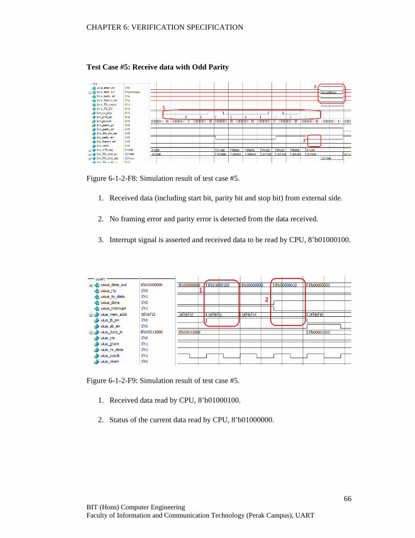
CHAPTER 6: VERIFICATION SPECIFICATION
66 BIT (Hons) Computer Engineering Faculty of Information and Communication Technology (Perak Campus), UART
Test Case #5: Receive data with Odd Parity
Figure 6-1-2-F8: Simulation result of test case #5.
1. Received data (including start bit, parity bit and stop bit) from external side.
2. No framing error and parity error is detected from the data received.
3. Interrupt signal is asserted and received data to be read by CPU, 8’b01000100.
Figure 6-1-2-F9: Simulation result of test case #5.
1. Received data read by CPU, 8’b01000100.
2. Status of the current data read by CPU, 8’b01000000.
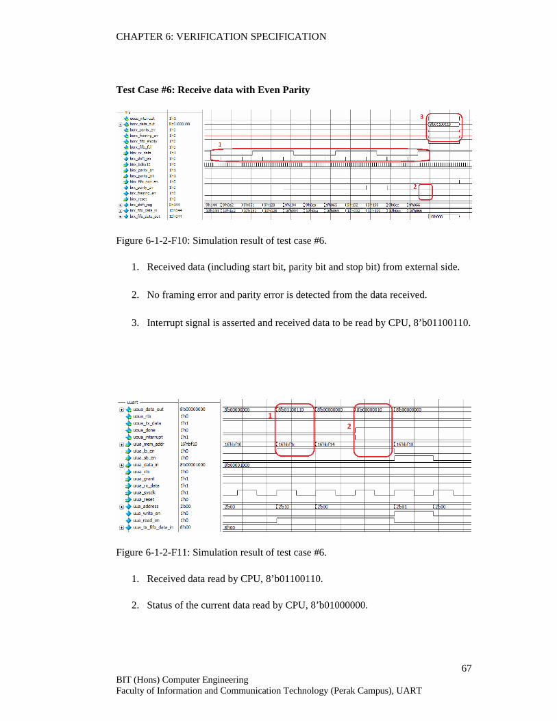
CHAPTER 6: VERIFICATION SPECIFICATION
67 BIT (Hons) Computer Engineering Faculty of Information and Communication Technology (Perak Campus), UART
Test Case #6: Receive data with Even Parity
Figure 6-1-2-F10: Simulation result of test case #6.
1. Received data (including start bit, parity bit and stop bit) from external side.
2. No framing error and parity error is detected from the data received.
3. Interrupt signal is asserted and received data to be read by CPU, 8’b01100110.
Figure 6-1-2-F11: Simulation result of test case #6.
1. Received data read by CPU, 8’b01100110.
2. Status of the current data read by CPU, 8’b01000000.

CHAPTER 6: VERIFICATION SPECIFICATION
68 BIT (Hons) Computer Engineering Faculty of Information and Communication Technology (Perak Campus), UART
Test Case #7: Receive data with no Parity
Figure 6-1-2-F12: Simulation result of test case #7
1. Received data (including start bit, parity bit and stop bit) from external side.
2. No framing error and parity error is detected from the data received.
3. Interrupt signal is asserted and received data to be read by CPU, 8’b10011001.
Figure 6-1-2-F13: Simulation result of test case #7.
1. Received data read by CPU, 8’b10011001.
2. Status of the current data read by CPU, 8’b00000000.
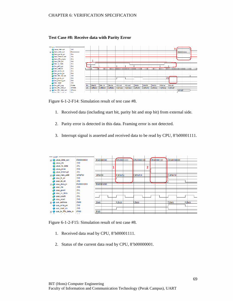
CHAPTER 6: VERIFICATION SPECIFICATION
69 BIT (Hons) Computer Engineering Faculty of Information and Communication Technology (Perak Campus), UART
Test Case #8: Receive data with Parity Error
Figure 6-1-2-F14: Simulation result of test case #8.
1. Received data (including start bit, parity bit and stop bit) from external side.
2. Parity error is detected in this data. Framing error is not detected.
3. Interrupt signal is asserted and received data to be read by CPU, 8’b00001111.
Figure 6-1-2-F15: Simulation result of test case #8.
1. Received data read by CPU, 8’b00001111.
2. Status of the current data read by CPU, 8’b00000001.
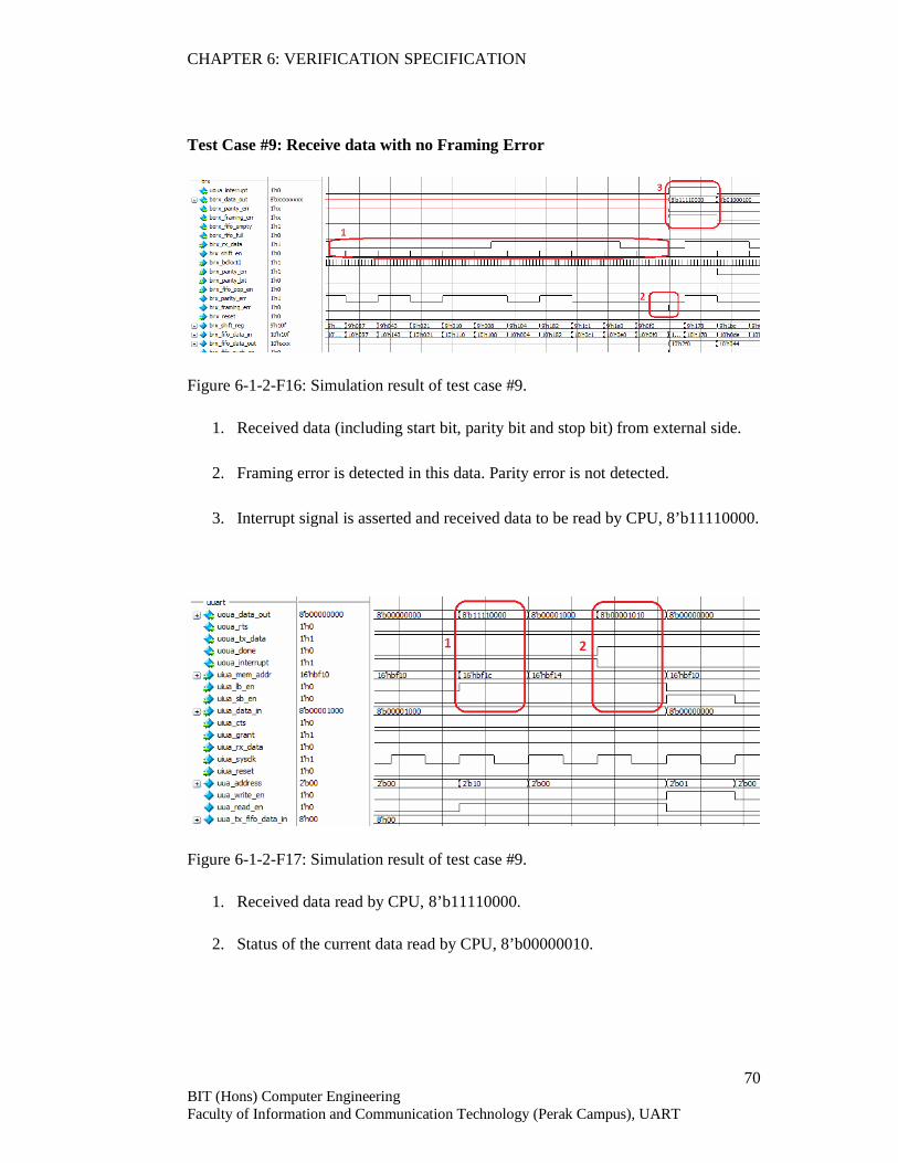
CHAPTER 6: VERIFICATION SPECIFICATION
70 BIT (Hons) Computer Engineering Faculty of Information and Communication Technology (Perak Campus), UART
Test Case #9: Receive data with no Framing Error
Figure 6-1-2-F16: Simulation result of test case #9.
1. Received data (including start bit, parity bit and stop bit) from external side.
2. Framing error is detected in this data. Parity error is not detected.
3. Interrupt signal is asserted and received data to be read by CPU, 8’b11110000.
Figure 6-1-2-F17: Simulation result of test case #9.
1. Received data read by CPU, 8’b11110000.
2. Status of the current data read by CPU, 8’b00000010.

CHAPTER 6: VERIFICATION SPECIFICATION
71 BIT (Hons) Computer Engineering Faculty of Information and Communication Technology (Perak Campus), UART
6-1-3 Testbench Code of UART Test
//********************************** // Define declaration. //********************************** `include "../util/macro.v" //********************************** // Test Bench for Transmitter. //********************************** module tb_uuart (); //********************************** // Wire declaration. //********************************** wire [`BYTE_NB - 1 : 0] tb_data_out; wire tb_rts; wire tb_tx_data; wire tb_interrupt; //********************************** // Register declaration. //********************************** reg [15 : 0] tb_mem_addr; reg [`BYTE_NB + 3 : 0] tb_test_data; reg [`BYTE_NB - 1 : 0] tb_data_in; reg tb_rx_data; reg tb_cts; reg tb_lb_en; reg tb_sb_en; reg tb_sysclk; reg tb_reset; //********************************** // Instantiation Of Module. //********************************** uuart dut_uart (.uoua_data_out(tb_data_out), .uoua_tx_data(tb_tx_data),
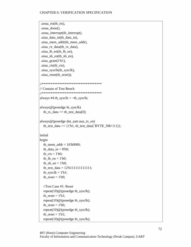
CHAPTER 6: VERIFICATION SPECIFICATION
72 BIT (Hons) Computer Engineering Faculty of Information and Communication Technology (Perak Campus), UART
.uoua_rts(tb_rts), .uoua_done(), .uoua_interrupt(tb_interrupt), .uiua_data_in(tb_data_in), .uiua_mem_addr(tb_mem_addr), .uiua_rx_data(tb_rx_data), .uiua_lb_en(tb_lb_en), .uiua_sb_en(tb_sb_en), .uiua_grant(1'b1), .uiua_cts(tb_cts), .uiua_sysclk(tb_sysclk), .uiua_reset(tb_reset)); //********************************** // Contain of Test Bench //********************************** always #4 tb_sysclk = ~tb_sysclk; always@(posedge tb_sysclk) tb_rx_data <= tb_test_data[0]; always@(posedge dut_uart.uua_tx_en) tb_test_data <= {1'b1, tb_test_data[`BYTE_NB+3:1]}; initial begin tb_mem_addr = 16'h0000; tb_data_in = 8'b0; tb_cts = 1'b0; tb_lb_en = 1'b0; tb_sb_en = 1'b0; tb_test_data = 12'b111111111111; tb_sysclk = 1'b1; tb_reset = 1'b0; //Test Case #1: Reset repeat(10)@(posedge tb_sysclk); tb_reset = 1'b1; repeat(10)@(posedge tb_sysclk); tb_reset = 1'b0; repeat(10)@(posedge tb_sysclk); tb_reset = 1'b1; repeat(10)@(posedge tb_sysclk);
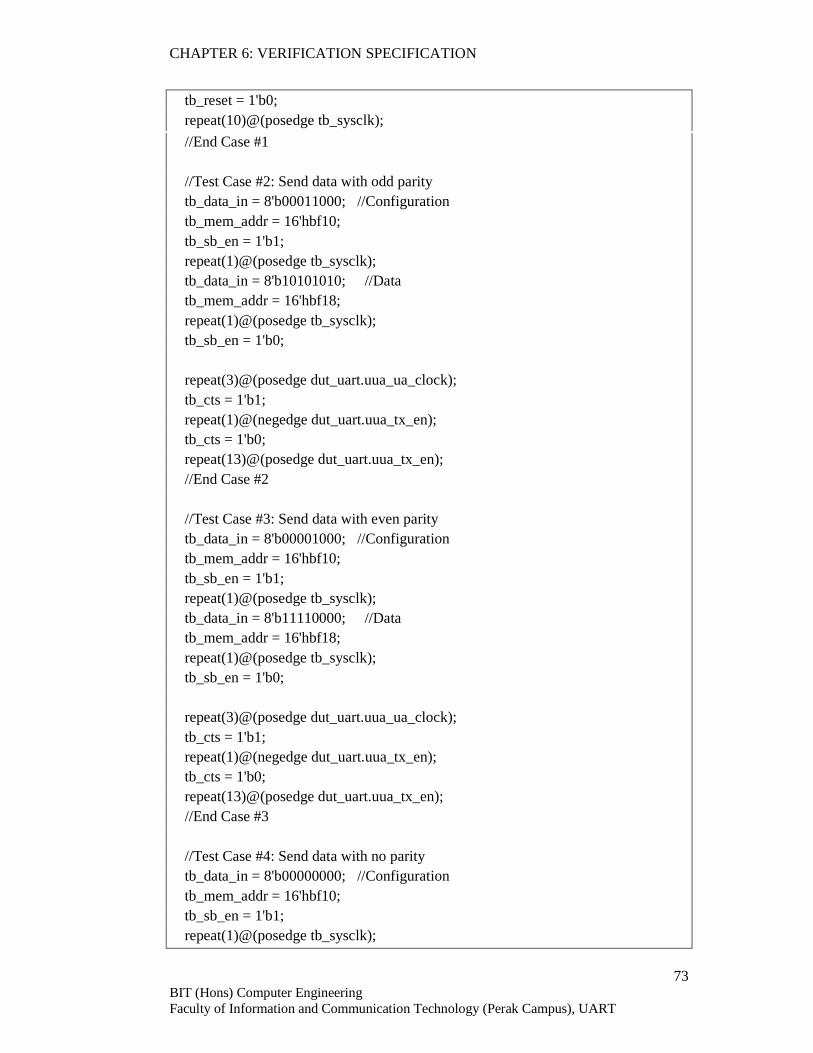
CHAPTER 6: VERIFICATION SPECIFICATION
73 BIT (Hons) Computer Engineering Faculty of Information and Communication Technology (Perak Campus), UART
tb_reset = 1'b0; repeat(10)@(posedge tb_sysclk);
//End Case #1 //Test Case #2: Send data with odd parity tb_data_in = 8'b00011000; //Configuration tb_mem_addr = 16'hbf10; tb_sb_en = 1'b1; repeat(1)@(posedge tb_sysclk); tb_data_in = 8'b10101010; //Data tb_mem_addr = 16'hbf18; repeat(1)@(posedge tb_sysclk); tb_sb_en = 1'b0; repeat(3)@(posedge dut_uart.uua_ua_clock); tb_cts = 1'b1; repeat(1)@(negedge dut_uart.uua_tx_en); tb_cts = 1'b0; repeat(13)@(posedge dut_uart.uua_tx_en); //End Case #2 //Test Case #3: Send data with even parity tb_data_in = 8'b00001000; //Configuration tb_mem_addr = 16'hbf10; tb_sb_en = 1'b1; repeat(1)@(posedge tb_sysclk); tb_data_in = 8'b11110000; //Data tb_mem_addr = 16'hbf18; repeat(1)@(posedge tb_sysclk); tb_sb_en = 1'b0; repeat(3)@(posedge dut_uart.uua_ua_clock); tb_cts = 1'b1; repeat(1)@(negedge dut_uart.uua_tx_en); tb_cts = 1'b0; repeat(13)@(posedge dut_uart.uua_tx_en); //End Case #3 //Test Case #4: Send data with no parity tb_data_in = 8'b00000000; //Configuration tb_mem_addr = 16'hbf10; tb_sb_en = 1'b1; repeat(1)@(posedge tb_sysclk);
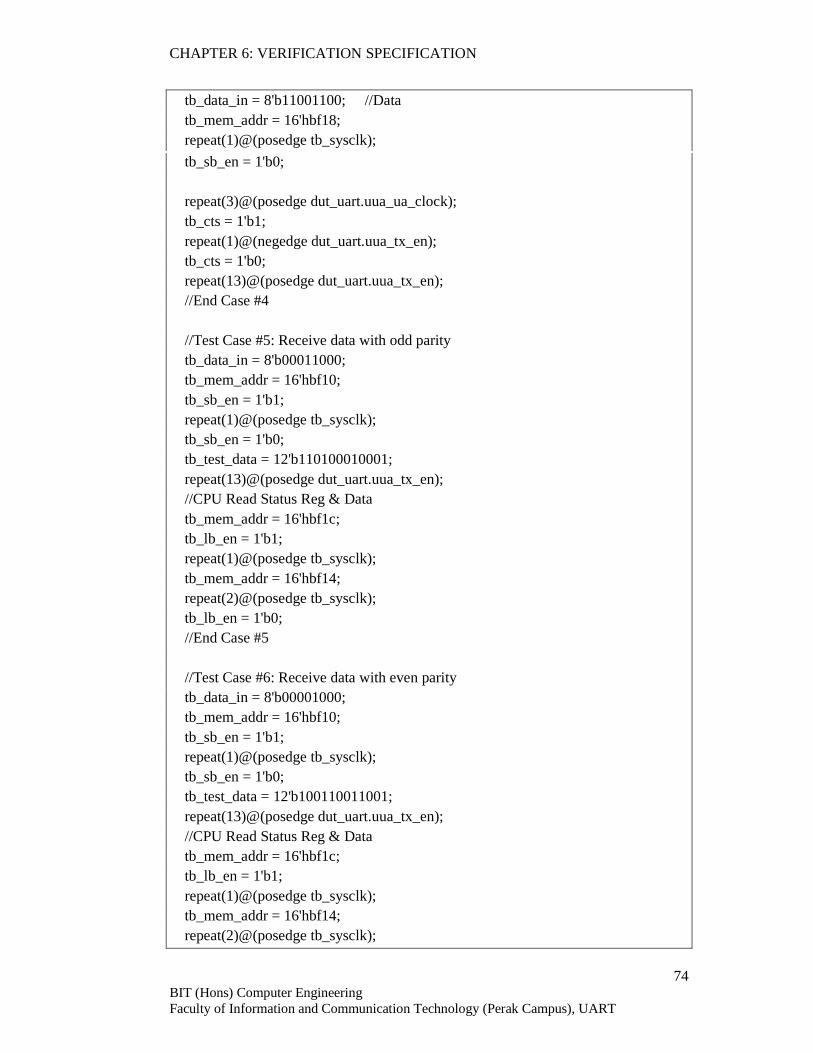
CHAPTER 6: VERIFICATION SPECIFICATION
74 BIT (Hons) Computer Engineering Faculty of Information and Communication Technology (Perak Campus), UART
tb_data_in = 8'b11001100; //Data tb_mem_addr = 16'hbf18; repeat(1)@(posedge tb_sysclk);
tb_sb_en = 1'b0; repeat(3)@(posedge dut_uart.uua_ua_clock); tb_cts = 1'b1; repeat(1)@(negedge dut_uart.uua_tx_en); tb_cts = 1'b0; repeat(13)@(posedge dut_uart.uua_tx_en); //End Case #4 //Test Case #5: Receive data with odd parity tb_data_in = 8'b00011000; tb_mem_addr = 16'hbf10; tb_sb_en = 1'b1; repeat(1)@(posedge tb_sysclk); tb_sb_en = 1'b0; tb_test_data = 12'b110100010001; repeat(13)@(posedge dut_uart.uua_tx_en); //CPU Read Status Reg & Data tb_mem_addr = 16'hbf1c; tb_lb_en = 1'b1; repeat(1)@(posedge tb_sysclk); tb_mem_addr = 16'hbf14; repeat(2)@(posedge tb_sysclk); tb_lb_en = 1'b0; //End Case #5 //Test Case #6: Receive data with even parity tb_data_in = 8'b00001000; tb_mem_addr = 16'hbf10; tb_sb_en = 1'b1; repeat(1)@(posedge tb_sysclk); tb_sb_en = 1'b0; tb_test_data = 12'b100110011001; repeat(13)@(posedge dut_uart.uua_tx_en); //CPU Read Status Reg & Data tb_mem_addr = 16'hbf1c; tb_lb_en = 1'b1; repeat(1)@(posedge tb_sysclk); tb_mem_addr = 16'hbf14; repeat(2)@(posedge tb_sysclk);

CHAPTER 6: VERIFICATION SPECIFICATION
75 BIT (Hons) Computer Engineering Faculty of Information and Communication Technology (Perak Campus), UART
tb_lb_en = 1'b0; //End Case #6 //Test Case #7: Receive data with no parity
tb_data_in = 8'b00000000; tb_mem_addr = 16'hbf10; tb_sb_en = 1'b1; repeat(1)@(posedge tb_sysclk); tb_sb_en = 1'b0; tb_test_data = 12'b111001100101; repeat(13)@(posedge dut_uart.uua_tx_en); //CPU Read Status Reg & Data tb_mem_addr = 16'hbf1c; tb_lb_en = 1'b1; repeat(1)@(posedge tb_sysclk); tb_mem_addr = 16'hbf14; repeat(2)@(posedge tb_sysclk); tb_lb_en = 1'b0; //End Case #7 //Test Case #8: Receive data with parity error tb_data_in = 8'b00001000; tb_mem_addr = 16'hbf10; tb_sb_en = 1'b1; repeat(1)@(posedge tb_sysclk); tb_sb_en = 1'b0; tb_test_data = 12'b110000111101; repeat(13)@(posedge dut_uart.uua_tx_en); //CPU Read Status Reg & Data tb_mem_addr = 16'hbf1c; tb_lb_en = 1'b1; repeat(1)@(posedge tb_sysclk); tb_mem_addr = 16'hbf14; repeat(2)@(posedge tb_sysclk); tb_lb_en = 1'b0; //End Case #8 //Test Case #9: Receive data with framing error tb_data_in = 8'b00001000; tb_mem_addr = 16'hbf10; tb_sb_en = 1'b1; repeat(1)@(posedge tb_sysclk); tb_sb_en = 1'b0;
CHAPTER 6: VERIFICATION SPECIFICATION
76 BIT (Hons) Computer Engineering Faculty of Information and Communication Technology (Perak Campus), UART
tb_test_data = 12'b001111000001; repeat(13)@(posedge dut_uart.uua_tx_en); //CPU Read Status Reg & Data tb_mem_addr = 16'hbf1c; tb_lb_en = 1'b1;
repeat(1)@(posedge tb_sysclk); tb_mem_addr = 16'hbf14; repeat(2)@(posedge tb_sysclk); tb_lb_en = 1'b0; //End Case #9 repeat(10)@(posedge tb_sysclk); $stop; end endmodule
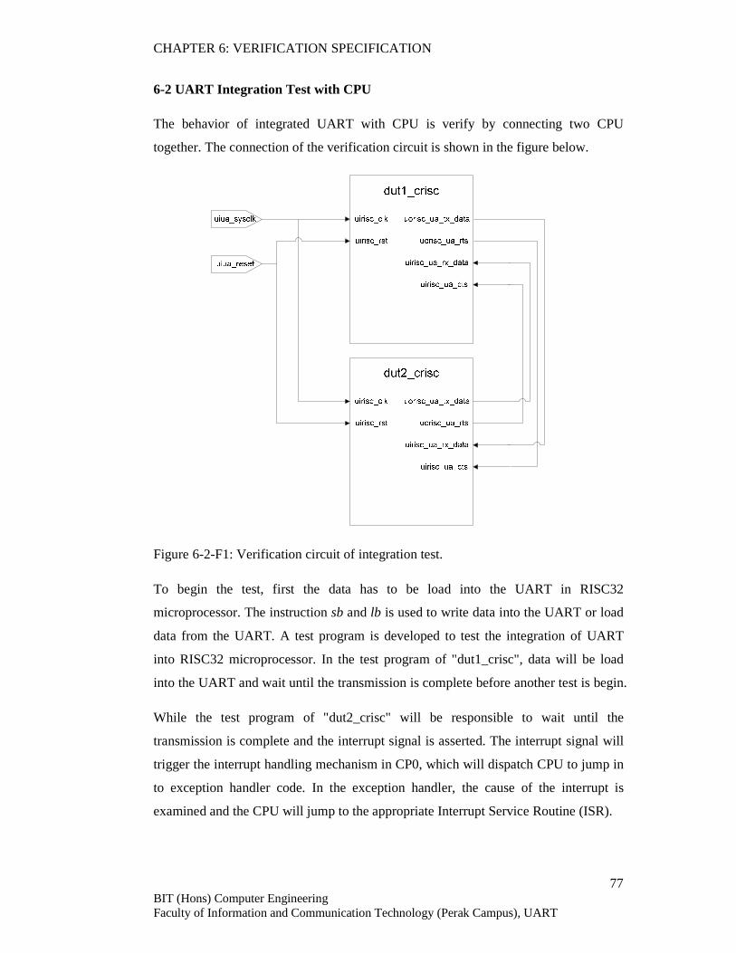
CHAPTER 6: VERIFICATION SPECIFICATION
77 BIT (Hons) Computer Engineering Faculty of Information and Communication Technology (Perak Campus), UART
6-2 UART Integration Test with CPU
The behavior of integrated UART with CPU is verify by connecting two CPU
together. The connection of the verification circuit is shown in the figure below.
Figure 6-2-F1: Verification circuit of integration test.
To begin the test, first the data has to be load into the UART in RISC32
microprocessor. The instruction sb and lb is used to write data into the UART or load
data from the UART. A test program is developed to test the integration of UART
into RISC32 microprocessor. In the test program of "dut1_crisc", data will be load
into the UART and wait until the transmission is complete before another test is begin.
While the test program of "dut2_crisc" will be responsible to wait until the
transmission is complete and the interrupt signal is asserted. The interrupt signal will
trigger the interrupt handling mechanism in CP0, which will dispatch CPU to jump in
to exception handler code. In the exception handler, the cause of the interrupt is
examined and the CPU will jump to the appropriate Interrupt Service Routine (ISR).
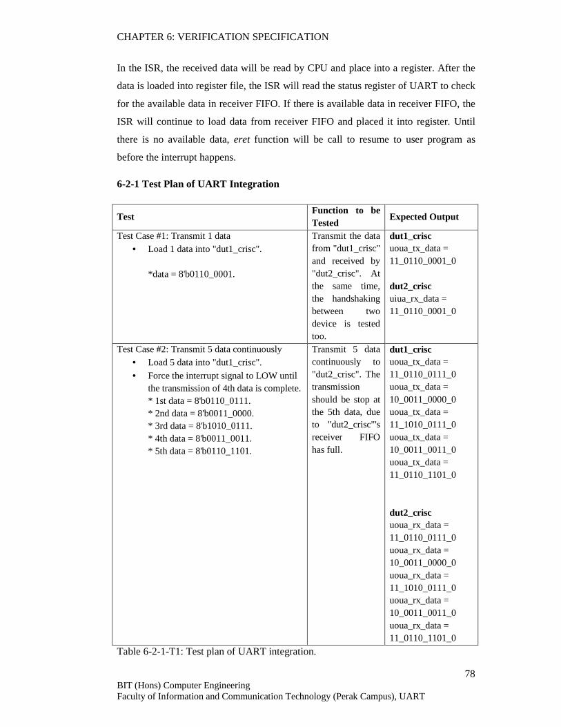
CHAPTER 6: VERIFICATION SPECIFICATION
78 BIT (Hons) Computer Engineering Faculty of Information and Communication Technology (Perak Campus), UART
In the ISR, the received data will be read by CPU and place into a register. After the
data is loaded into register file, the ISR will read the status register of UART to check
for the available data in receiver FIFO. If there is available data in receiver FIFO, the
ISR will continue to load data from receiver FIFO and placed it into register. Until
there is no available data, eret function will be call to resume to user program as
before the interrupt happens.
6-2-1 Test Plan of UART Integration
Test Function to be Tested
Expected Output
Test Case #1: Transmit 1 data • Load 1 data into "dut1_crisc".
*data = 8'b0110_0001.
Transmit the data from "dut1_crisc" and received by "dut2_crisc". At the same time, the handshaking between two device is tested too.
dut1_crisc uoua_tx_data = 11_0110_0001_0 dut2_crisc uiua_rx_data = 11_0110_0001_0
Test Case #2: Transmit 5 data continuously • Load 5 data into "dut1_crisc".
• Force the interrupt signal to LOW until the transmission of 4th data is complete. * 1st data = 8'b0110_0111. * 2nd data = 8'b0011_0000. * 3rd data = 8'b1010_0111. * 4th data = 8'b0011_0011. * 5th data = 8'b0110_1101.
Transmit 5 data continuously to "dut2_crisc". The transmission should be stop at the 5th data, due to "dut2_crisc"'s receiver FIFO has full.
dut1_crisc uoua_tx_data = 11_0110_0111_0 uoua_tx_data = 10_0011_0000_0 uoua_tx_data = 11_1010_0111_0 uoua_tx_data = 10_0011_0011_0 uoua_tx_data = 11_0110_1101_0 dut2_crisc uoua_rx_data = 11_0110_0111_0 uoua_rx_data = 10_0011_0000_0 uoua_rx_data = 11_1010_0111_0 uoua_rx_data = 10_0011_0011_0 uoua_rx_data = 11_0110_1101_0
Table 6-2-1-T1: Test plan of UART integration.

CHAPTER 6: VERIFICATION SPECIFICATION
79 BIT (Hons) Computer Engineering Faculty of Information and Communication Technology (Perak Campus), UART
6-2-2 Test Program of "dut1_crisc"
.text 0x00400024 .globl main main: lui $t0, 0xbf00 ori $s0, $t0, 0x000c #base address of UART memory map addi $t0, $zero, 0x8 #even parity, 38400 baud speed sb $t0, 4($s0) #write configuration to config reg #test case #1: Transmit 1 data test1: addi $t0, $zero, 0x61 #data 1: 0110_0001 sb $t0, 12($s0) addi $t0, $zero, 6500 wait1: addi $t0, $t0, -1 #wait for UART transmit 1 data bne $t0, $zero, wait1 nop #test case #2: Transmit 5 data continuously test2: addi $t0, $zero, 0x67 #data 1: 0110_0111 addi $t1, $zero, 0x30 #data 2: 0011_0000 addi $t2, $zero, 0xa7 #data 3: 1010_0111 addi $t3, $zero, 0x33 #data 4: 0011_0011 addi $t4, $zero, 0x6d #data 5: 0110_1101 sb $t0, 12($s0) sb $t1, 12($s0) sb $t2, 12($s0) sb $t3, 12($s0) addi $t0, $zero, 6500 wait2: addi $t0, $t0, -1 #wait for UART transmit 1 data bne $t0, $zero, wait2 nop sb $t4, 12($s0) addi $t0, $zero, 26500 wait3: addi $t0, $t0, -1 #wait for UART transmit 4 data bne $t0, $zero, wait3 nop exit: j exit nop
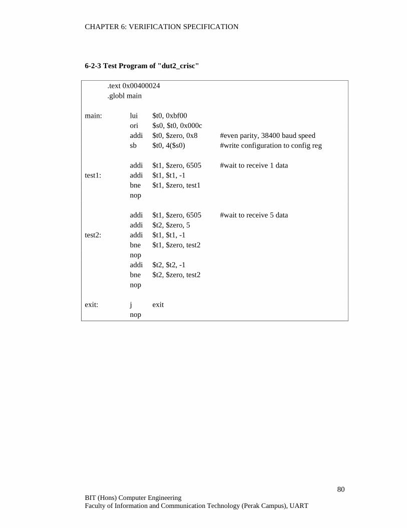
CHAPTER 6: VERIFICATION SPECIFICATION
80 BIT (Hons) Computer Engineering Faculty of Information and Communication Technology (Perak Campus), UART
6-2-3 Test Program of "dut2_crisc"
.text 0x00400024 .globl main main: lui $t0, 0xbf00 ori $s0, $t0, 0x000c addi $t0, $zero, 0x8 #even parity, 38400 baud speed sb $t0, 4($s0) #write configuration to config reg addi $t1, $zero, 6505 #wait to receive 1 data test1: addi $t1, $t1, -1 bne $t1, $zero, test1 nop addi $t1, $zero, 6505 #wait to receive 5 data addi $t2, $zero, 5 test2: addi $t1, $t1, -1 bne $t1, $zero, test2 nop addi $t2, $t2, -1 bne $t2, $zero, test2 nop exit: j exit nop

CHAPTER 6: VERIFICATION SPECIFICATION
81 BIT (Hons) Computer Engineering Faculty of Information and Communication Technology (Perak Campus), UART
6-2-4 Pseudocode of Exception Handler
BEGIN
STORE current status of user program
Extract Exception Code of Cause Register
CASE of Exception Code OF
0: Branch to exception routine of Interrupt
4: Branch to exception routine of Address Error Trap LOAD
5: Branch to exception routine of Address Error Trap STORE
6: Branch to exception routine of Bus Error on IF Trap
7: Branch to exception routine of Bus Error on LOAD/STORE Trap
8: Branch to exception routine of Syscall
9: Branch to exception routine of Breakpoint Trap
10: Branch to exception routine of Reserved/Undefined Instruction
12: Branch to exception routine of Arithmetic Overflow
ENDCASE
Read Status Register to default state
Read Cause Register to default state
Restore state of user program
Increment EPC address by 4
Return the user program based on EPC register address
END
6-2-5 Pseudocode of UART ISR
BEGIN
LOAD base address of UART memory map
LOAD received data
Extract the UART receiver FIFO status from UART status register
IF receiver FIFO is not empty THEN
JUMP to the begin of ISR
ENDIF
Return to main exception handler code

CHAPTER 6: VERIFICATION SPECIFICATION
82 BIT (Hons) Computer Engineering Faculty of Information and Communication Technology (Perak Campus), UART
END

CHAPTER 6: VERIFICATION SPECIFICATION
83 BIT (Hons) Computer Engineering Faculty of Information and Communication Technology (Perak Campus), UART
6-2-6 Simulation Result
Test Case #1: Transmit 1 data
Figure 6-2-6-F1: Simulation result of test case #1.
1. Transmitting data from dut1_crisc to dut2_crisc. Data = 11_0110_0001_0.
2. Received data from dut1_crisc.
3. Interrupt signal is asserted after dut2_crisc received the data from dut1_crisc.

CHAPTER 6: VERIFICATION SPECIFICATION
84 BIT (Hons) Computer Engineering Faculty of Information and Communication Technology (Perak Campus), UART
Figure 6-2-6-F1: Simulation result of test case #1.
1. After the interrupt signal is asserted, the urisc_pc changes from normal program execution to the first line of the exception handler code,
which is from 32'h0040_0050 to 32'h8000_0180.
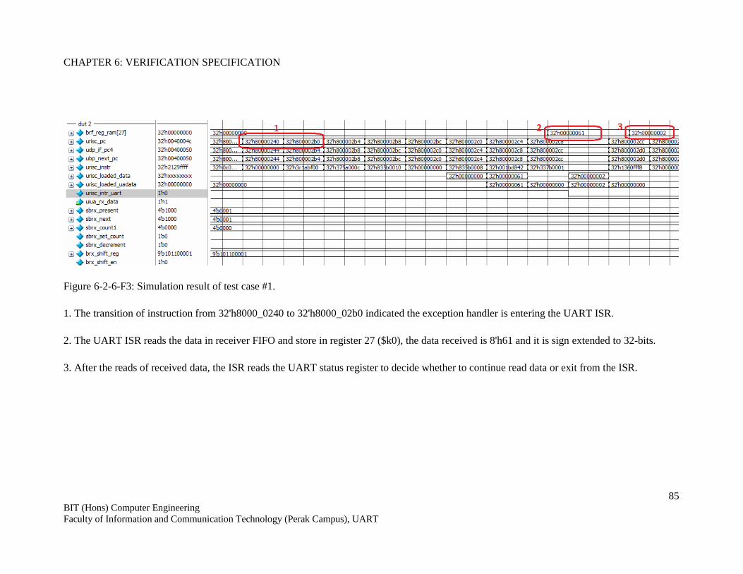
CHAPTER 6: VERIFICATION SPECIFICATION
85 BIT (Hons) Computer Engineering Faculty of Information and Communication Technology (Perak Campus), UART
Figure 6-2-6-F3: Simulation result of test case #1.
1. The transition of instruction from 32'h8000_0240 to 32'h8000_02b0 indicated the exception handler is entering the UART ISR.
2. The UART ISR reads the data in receiver FIFO and store in register 27 ($k0), the data received is 8'h61 and it is sign extended to 32-bits.
3. After the reads of received data, the ISR reads the UART status register to decide whether to continue read data or exit from the ISR.
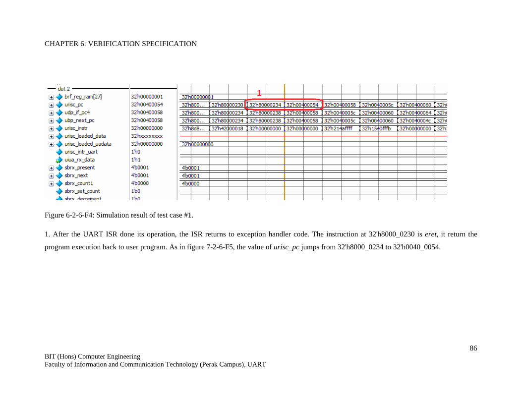
CHAPTER 6: VERIFICATION SPECIFICATION
86 BIT (Hons) Computer Engineering Faculty of Information and Communication Technology (Perak Campus), UART
Figure 6-2-6-F4: Simulation result of test case #1.
1. After the UART ISR done its operation, the ISR returns to exception handler code. The instruction at 32'h8000_0230 is eret, it return the
program execution back to user program. As in figure 7-2-6-F5, the value of urisc_pc jumps from 32'h8000_0234 to 32'h0040_0054.
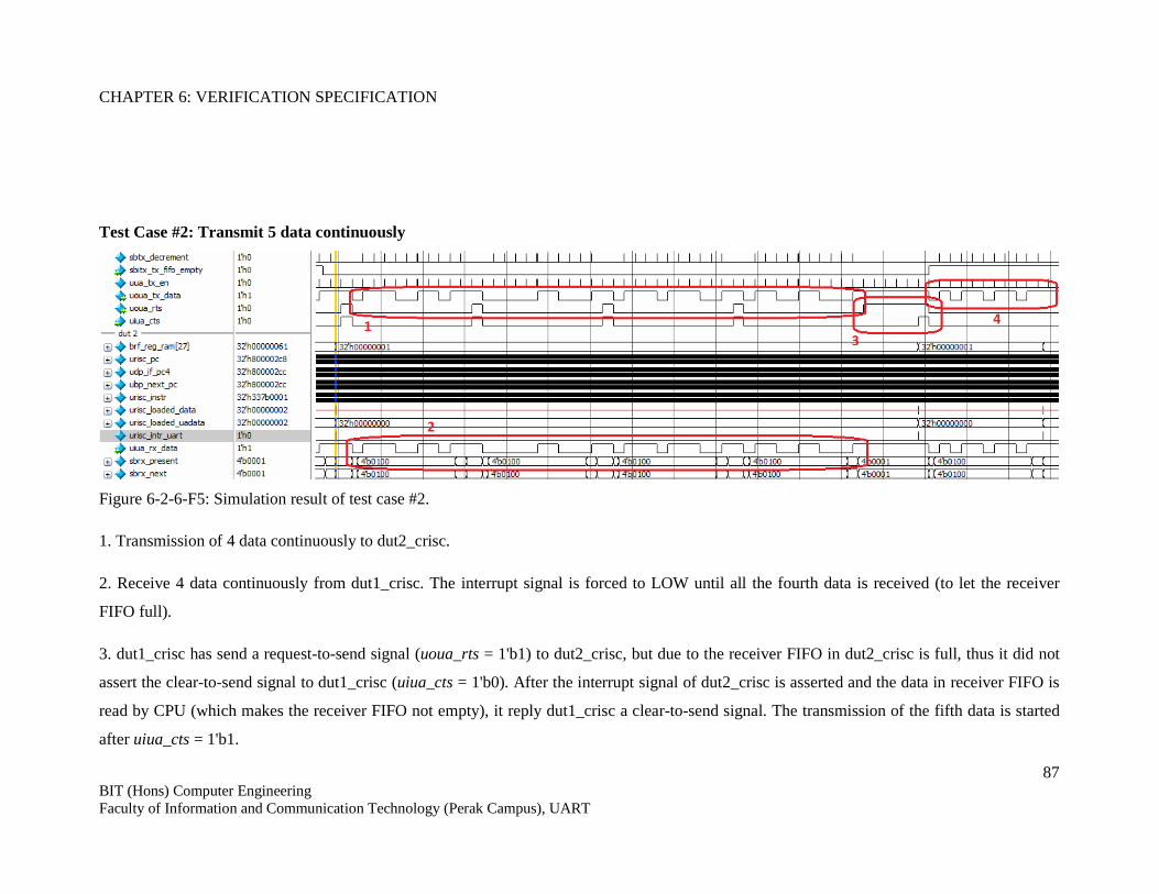
CHAPTER 6: VERIFICATION SPECIFICATION
87 BIT (Hons) Computer Engineering Faculty of Information and Communication Technology (Perak Campus), UART
Test Case #2: Transmit 5 data continuously
Figure 6-2-6-F5: Simulation result of test case #2.
1. Transmission of 4 data continuously to dut2_crisc.
2. Receive 4 data continuously from dut1_crisc. The interrupt signal is forced to LOW until all the fourth data is received (to let the receiver
FIFO full).
3. dut1_crisc has send a request-to-send signal (uoua_rts = 1'b1) to dut2_crisc, but due to the receiver FIFO in dut2_crisc is full, thus it did not
assert the clear-to-send signal to dut1_crisc (uiua_cts = 1'b0). After the interrupt signal of dut2_crisc is asserted and the data in receiver FIFO is
read by CPU (which makes the receiver FIFO not empty), it reply dut1_crisc a clear-to-send signal. The transmission of the fifth data is started
after uiua_cts = 1'b1.
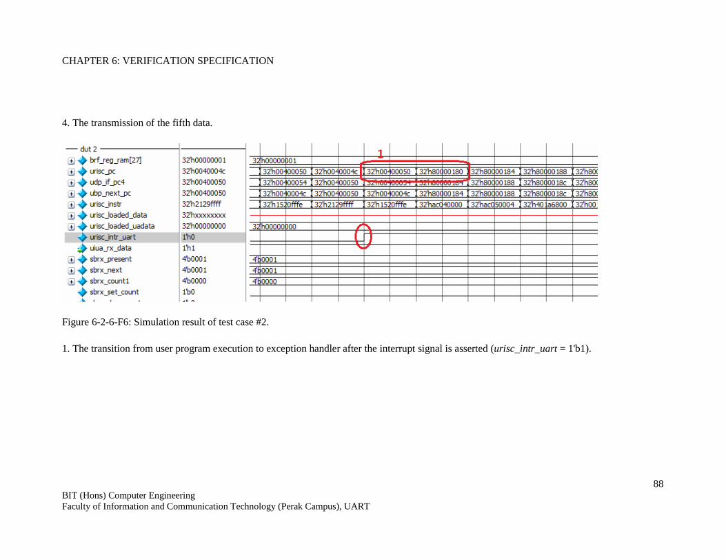
CHAPTER 6: VERIFICATION SPECIFICATION
88 BIT (Hons) Computer Engineering Faculty of Information and Communication Technology (Perak Campus), UART
4. The transmission of the fifth data.
Figure 6-2-6-F6: Simulation result of test case #2.
1. The transition from user program execution to exception handler after the interrupt signal is asserted (urisc_intr_uart = 1'b1).

CHAPTER 6: VERIFICATION SPECIFICATION
89 BIT (Hons) Computer Engineering Faculty of Information and Communication Technology (Perak Campus), UART
Figure 6-2-6-F7: Simulation result of test case #2.
1. The second data and the value of status register is read by CPU. The status register value indicate that the receiver FIFO is not empty, thus the
UART ISR will jump back to the beginning of ISR instead of jumping back to exception handler code.
2. The program execution jump to the beginning of the UART ISR.

CHAPTER 6: VERIFICATION SPECIFICATION
90 BIT (Hons) Computer Engineering Faculty of Information and Communication Technology (Perak Campus), UART
Figure 6-2-6-F8: Simulation result of rest case #2.
1. Continuous reading of data and status register until the receiver FIFO is empty.
2. The interrupt signal is de-asserted after all the data in receiver FIFO is read.

CHAPTER 6: VERIFICATION SPECIFICATION
91 BIT (Hons) Computer Engineering Faculty of Information and Communication Technology (Perak Campus), UART
Figure 6-2-6-F9: Simulation result of test case #2.
1. CPU read the fifth data and its status.
2. The interrupt signal is de-asserted after CPU read the data from receiver FIFO.
CHAPTER 6: VERIFICATION SPECIFICATION
92 BIT (Hons) Computer Engineering Faculty of Information and Communication Technology (Perak Campus), UART
6-2-7 Testbench Code of UART Integration Test
//************************************************* ************* /* Project/Module: tb_r32_pipeline File Name: tb_r32_pipeline.v Date Created: 22/8/2016 Author: Lee Zhi Yong Description: RISC32 microprocessor with UART integrated testbench in Verilog code. */ //************************************************* ************* `include "../util/macro.v" module tb_r32_pipeline(); //declaration //======= INPUT ======= // System signal reg tb_u_clk; reg tb_u_rst; // UART signal reg tb_u_reset; wire dut1_tx_data; wire dut1_rts; wire dut2_tx_data; wire dut2_rts; //============================== // INSTANTIATION //============================== crisc dut1_crisc (// UART signal .uorisc_ua_tx_data(dut1_tx_data), .uorisc_ua_rts(dut1_rts), .uirisc_ua_rx_data(dut2_tx_data), .uirisc_ua_cts(dut2_rts), //======= INPUT ======= // System signal .uirisc_clk(tb_u_clk), .uirisc_rst(tb_u_rst) );
CHAPTER 6: VERIFICATION SPECIFICATION
93 BIT (Hons) Computer Engineering Faculty of Information and Communication Technology (Perak Campus), UART
crisc dut2_crisc
(// UART signal .uorisc_ua_tx_data(dut2_tx_data), .uorisc_ua_rts(dut2_rts), .uirisc_ua_rx_data(dut1_tx_data), .uirisc_ua_cts(dut1_rts), //======= INPUT ======= // System signal .uirisc_clk(tb_u_clk), .uirisc_rst(tb_u_rst) ); //************************************ //Clock waveform generation initial tb_u_clk <= 1'b1; always #10 tb_u_clk =~ tb_u_clk; //~~~~~~~~~~~~~~~~~~~~~~~~~~~~~~~ // Signals initialization. //~~~~~~~~~~~~~~~~~~~~~~~~~~~~~~~ //======================== //read memory to get instruction initial begin //UART integration test by Lee Zhi Yong (201605) //DUT 1 $readmemh("test_loader_new.txt",tb_r32_pipeline.dut1_crisc.rom.data_ram); $readmemh("exc_handler.mips",tb_r32_pipeline.dut1_crisc.u_ktext_kseg0.u_cm_r_memory); $readmemh("test_program.txt",tb_r32_pipeline.dut1_crisc.u_text_seg.u_cm_r_memory); //DUT 2 $readmemh("test_loader_new.txt",tb_r32_pipeline.dut2_crisc.rom.data_ram); $readmemh("exc_handler.mips",tb_r32_pipeline.dut2_crisc.u_ktext_kseg0.u_cm_r_memory); $readmemh("uart_config.txt",tb_r32_pipeline.dut2_crisc.u_text_seg.u_cm_r_memory);
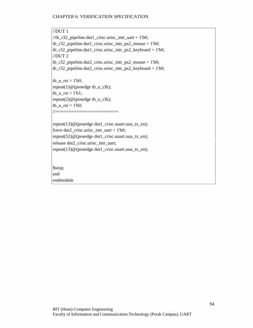
CHAPTER 6: VERIFICATION SPECIFICATION
94 BIT (Hons) Computer Engineering Faculty of Information and Communication Technology (Perak Campus), UART
//DUT 1 //tb_r32_pipeline.dut1_crisc.urisc_intr_uart = 1'b0; tb_r32_pipeline.dut1_crisc.urisc_intr_ps2_mouse = 1'b0; tb_r32_pipeline.dut1_crisc.urisc_intr_ps2_keyboard = 1'b0; //DUT 2 tb_r32_pipeline.dut2_crisc.urisc_intr_ps2_mouse = 1'b0; tb_r32_pipeline.dut2_crisc.urisc_intr_ps2_keyboard = 1'b0; tb_u_rst = 1'b0; repeat(1)@(posedge tb_u_clk); tb_u_rst = 1'b1; repeat(2)@(posedge tb_u_clk); tb_u_rst = 1'b0; //======================== repeat(13)@(posedge dut1_crisc.uuart.uua_tx_en); force dut2_crisc.urisc_intr_uart = 1'b0; repeat(52)@(posedge dut1_crisc.uuart.uua_tx_en);
release dut2_crisc.urisc_intr_uart; repeat(13)@(posedge dut1_crisc.uuart.uua_tx_en); $stop; end endmodule
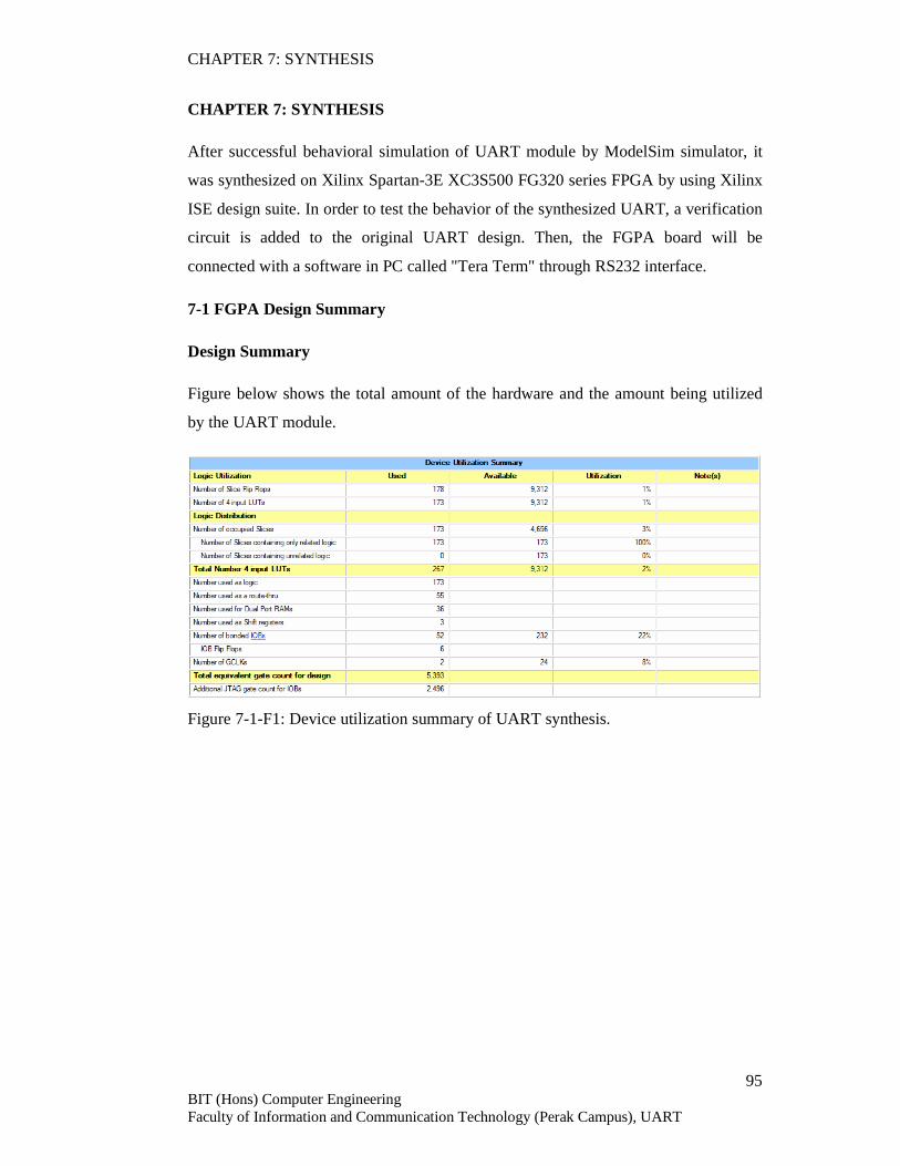
CHAPTER 7: SYNTHESIS
95 BIT (Hons) Computer Engineering Faculty of Information and Communication Technology (Perak Campus), UART
CHAPTER 7: SYNTHESIS
After successful behavioral simulation of UART module by ModelSim simulator, it
was synthesized on Xilinx Spartan-3E XC3S500 FG320 series FPGA by using Xilinx
ISE design suite. In order to test the behavior of the synthesized UART, a verification
circuit is added to the original UART design. Then, the FGPA board will be
connected with a software in PC called "Tera Term" through RS232 interface.
7-1 FGPA Design Summary
Design Summary
Figure below shows the total amount of the hardware and the amount being utilized
by the UART module.
Figure 7-1-F1: Device utilization summary of UART synthesis.

CHAPTER 7: SYNTHESIS
96 BIT (Hons) Computer Engineering Faculty of Information and Communication Technology (Perak Campus), UART
Pinout Report
Figure below is the placement and configuration of UART's input and output pins.
Figure 7-1-F2: IO pin report of UART synthesis.
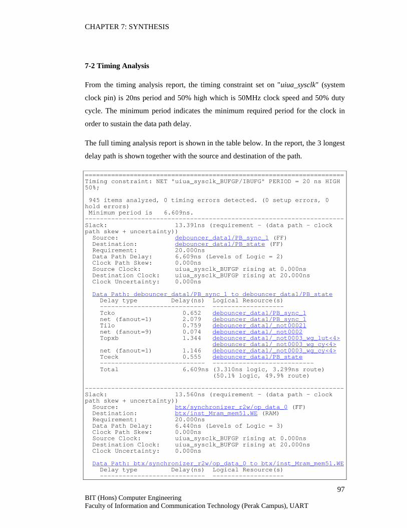
CHAPTER 7: SYNTHESIS
97 BIT (Hons) Computer Engineering Faculty of Information and Communication Technology (Perak Campus), UART
7-2 Timing Analysis
From the timing analysis report, the timing constraint set on "uiua_sysclk" (system
clock pin) is 20ns period and 50% high which is 50MHz clock speed and 50% duty
cycle. The minimum period indicates the minimum required period for the clock in
order to sustain the data path delay.
The full timing analysis report is shown in the table below. In the report, the 3 longest
delay path is shown together with the source and destination of the path.
===================================================================== Timing constraint: NET "uiua_sysclk_BUFGP/IBUFG" PERIOD = 20 ns HIGH 50%; 945 items analyzed, 0 timing errors detected. (0 setup errors, 0 hold errors) Minimum period is 6.609ns. --------------------------------------------------------------------- Slack: 13.391ns (requirement - (data path - clock path skew + uncertainty)) Source: debouncer_data1/PB_sync_1 (FF) Destination: debouncer_data1/PB_state (FF) Requirement: 20.000ns Data Path Delay: 6.609ns (Levels of Logic = 2) Clock Path Skew: 0.000ns Source Clock: uiua_sysclk_BUFGP rising at 0.000ns Destination Clock: uiua_sysclk_BUFGP rising at 20.000ns Clock Uncertainty: 0.000ns Data Path: debouncer_data1/PB_sync_1 to debouncer_data1/PB_state Delay type Delay(ns) Logical Resource(s) ---------------------------- ------------------- Tcko 0.652 debouncer_data1/PB_sync_1 net (fanout=1) 2.079 debouncer_data1/PB_sync_1 Tilo 0.759 debouncer_data1/_not00021 net (fanout=9) 0.074 debouncer_data1/_not0002 Topxb 1.344 debouncer_data1/_not0003_wg_lut<4> debouncer_data1/_not0003_wg_cy<4> net (fanout=1) 1.146 debouncer_data1/_not0003_wg_cy<4> Tceck 0.555 debouncer_data1/PB_state ---------------------------- --------------------------- Total 6.609ns (3.310ns logic, 3.299ns route) (50.1% logic, 49.9% route) --------------------------------------------------------------------- Slack: 13.560ns (requirement - (data path - clock path skew + uncertainty)) Source: btx/synchronizer_r2w/op_data_0 (FF) Destination: btx/inst_Mram_mem51.WE (RAM) Requirement: 20.000ns Data Path Delay: 6.440ns (Levels of Logic = 3) Clock Path Skew: 0.000ns Source Clock: uiua_sysclk_BUFGP rising at 0.000ns Destination Clock: uiua_sysclk_BUFGP rising at 20.000ns Clock Uncertainty: 0.000ns Data Path: btx/synchronizer_r2w/op_data_0 to btx/inst_Mram_mem51.WE Delay type Delay(ns) Logical Resource(s) ---------------------------- -------------------

CHAPTER 7: SYNTHESIS
98 BIT (Hons) Computer Engineering Faculty of Information and Communication Technology (Perak Campus), UART
Tcko 0.652 btx/synchronizer_r2w/op_data_0 net (fanout=2) 0.757 btx/synchronizer_r2w/op_data<0> Tilo 0.704 btx/asynfifo_r1_3/op_full_w_SW1 net (fanout=1) 0.762 N220 Tilo 0.704 btx/asynfifo_r1_3/op_full_w net (fanout=6) 0.099 uua_tx_fifo_full Tilo 0.704 btx/asynfifo_r1_3/w_inc_w1 net (fanout=8) 1.666 btx/asynfifo_r1_3/w_inc_w Tws 0.392 btx/inst_Mram_mem51.WE ---------------------------- --------------------------- Total 6.440ns (3.156ns logic, 3.284ns route) (49.0% logic, 51.0% route)
--------------------------------------------------------------------- Slack: 13.560ns (requirement - (data path - clock path skew + uncertainty)) Source: btx/synchronizer_r2w/op_data_0 (FF) Destination: btx/inst_Mram_mem61.WE (RAM) Requirement: 20.000ns Data Path Delay: 6.440ns (Levels of Logic = 3) Clock Path Skew: 0.000ns Source Clock: uiua_sysclk_BUFGP rising at 0.000ns Destination Clock: uiua_sysclk_BUFGP rising at 20.000ns Clock Uncertainty: 0.000ns Data Path: btx/synchronizer_r2w/op_data_0 to btx/inst_Mram_mem61.WE Delay type Delay(ns) Logical Resource(s) ---------------------------- ------------------- Tcko 0.652 btx/synchronizer_r2w/op_data_0 net (fanout=2) 0.757 btx/synchronizer_r2w/op_data<0> Tilo 0.704 btx/asynfifo_r1_3/op_full_w_SW1 net (fanout=1) 0.762 N220 Tilo 0.704 btx/asynfifo_r1_3/op_full_w net (fanout=6) 0.099 uua_tx_fifo_full Tilo 0.704 btx/asynfifo_r1_3/w_inc_w1 net (fanout=8) 1.666 btx/asynfifo_r1_3/w_inc_w Tws 0.392 btx/inst_Mram_mem61.WE ---------------------------- --------------------------- Total 6.440ns (3.156ns logic, 3.284ns route) (49.0% logic, 51.0% route) ---------------------------------------------------------------------
Table 7-2-T1: Timing analysis report of UART synthesis.

CHAPTER 7: SYNTHESIS
99 BIT (Hons) Computer Engineering Faculty of Information and Communication Technology (Perak Campus), UART
7-3 Power Analysis
The figure below is the power analysis report for this UART synthesis. The report
shows the estimation of power consumption of the design. Apart from that, the report
includes the thermal summary and decoupling network summary which shows the
estimated junction temperature and the capacitor recommended for the design.
Figure 7-3-F1: Power analysis report of UART synthesis.
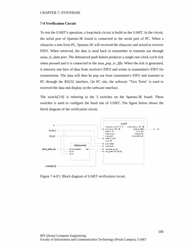
CHAPTER 7: SYNTHESIS
100 BIT (Hons) Computer Engineering Faculty of Information and Communication Technology (Perak Campus), UART
7-4 Verification Circuit
To test the UART's operation, a loop-back circuit is build on the UART. In the circuit,
the serial port of Spartan-3E board is connected to the serial port of PC. When a
character a sent from PC, Spartan-3E will received the character and stored in receiver
FIFO. When retrieved, the data is send back to transmitter to transmit out through
uoua_tx_data port. The debounced push button produces a single one-clock-cycle tick
when pressed and it is connected to the uiua_pop_rx_fifo. When the tick is generated,
it removes one byte of data from receiver's FIFO and writes to transmitter's FIFO for
transmission. The data will then be pop out from transmitter's FIFO and transmit to
PC through the RS232 interface. On PC site, the software "Tera Term" is used to
received the data and display on the software interface.
The switch[2:0] is referring to the 3 switches on the Spartan-3E board. These
switches is used to configure the baud rate of UART. The figure below shows the
block diagram of the verification circuit.
Figure 7-4-F1: Block diagram of UART verification circuit.

CHAPTER 7: SYNTHESIS
101 BIT (Hons) Computer Engineering Faculty of Information and Communication Technology (Perak Campus), UART
7-5 Setting Up the Testing Environment on PC
The software "Tera Term" is used to communicate with the synthesized UART on
Spartan-3E board. To be compatible with the UART on Spartan-3E board, it has to be
configured to the same configuration as the UART. By default, the UART
configuration is 9600 baud, 8 data bits, 1 stop bit and no parity. To configure the Tera
Term,
1. Open the software Tera Term from PC.
2. Select "Setup" from menu bar and click on "Serial port". A serial port setup
window will appears. Configure the setup as below:
• Port : COM5 (select the desired serial port)
• Baud rate : 9600
• Data : 8 bit
• Parity : none
• Stop : 1 bit
• Flow control : none
3. Click "Ok".
Now, the Tera Term is set up and ready to communicate with the Spartan-3E board.
Type any character on the software and press "Enter" to transmit to the board. The
configuration setting can be changed according to the configuration of the UART on
the board.
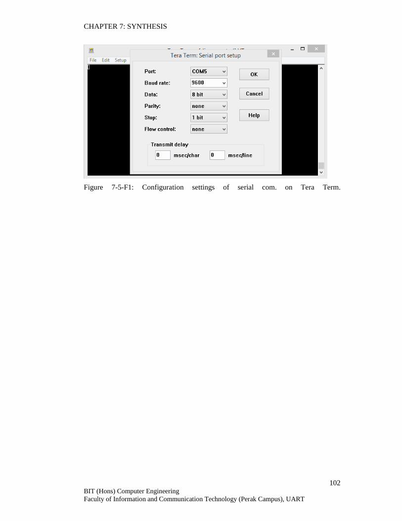
CHAPTER 7: SYNTHESIS
102 BIT (Hons) Computer Engineering Faculty of Information and Communication Technology (Perak Campus), UART
Figure 7-5-F1: Configuration settings of serial com. on Tera Term.
CHAPTER 8: CONCLUSION
103 BIT (Hons) Computer Engineering Faculty of Information and Communication Technology (Perak Campus), UART
CHAPTER 8: CONCLUSION
8-1 Conclusion
A UART module and a UART address decoder has been successfully modeled and
integrated into RISC32 microprocessor. All the behavior has been tested working.
The purpose of UART address decoder is to produce CPU Interface compatible output
signals to UART. Hence, the RISC32 microprocessor is able to communicate with
UART by using instruction sw to transmit data or configuration to UART and
instruction lw to read the 8-bits data or status from UART. The I/O serial
communication follows the protocol mentioned in Chapter 2 of this project.
The integration of UART into RISC32 architecture has been accomplished, as shown
is Chapter 4. In addition, the UART address decoder was modeled using Verilog HDL
based on the developed micro-architecture specification as shown in Chapter 5. The
full integration verification was also completed and its shown in Chapter 7. Apart
from that, the software handling part, which are the Exception Handler and Interrupt
Service Routine (ISR) are also proven to be working. The received data by UART
was successfully transferred to the register file.
The UART module has been successfully synthesized on Spartan-3E board by using
Xilinx ISE Foundation 8.2i software. An extra circuit is build in order to test the
functionality of synthesized UART, the circuit is shown in Chapter 7. The synthesized
UART is tested and proven to be working.
Based on the following table, the objectives stated in Chapter 1 has been achieved.
Table 8-1-T1: Enhancement outcome.
Objectives Status
Development of the RTL model of UART Enhanced
Integration of the UART model into existing RISC32 architecture Enhanced
Development of the Interrupt Service Routine (ISR) of UART Enhanced
Synthesis of UART on FPGA New
CHAPTER 8: CONCLUSION
104 BIT (Hons) Computer Engineering Faculty of Information and Communication Technology (Perak Campus), UART
8-2 Discussion and Future Work
The current design of the UART is not capable to handle the received data with parity
error or framing error. The error status is stored in status register but no action is
taken to the data. An error handling mechanism can be implement in future to handle
the data with error.
The Interrupt Service Routine (ISR) of UART is only able to read the receive data and
store in a register file. Further development should place the received data in memory
mapped address rather than a register file.
For future, the RISC32 microprocessor with I/O integrated can be synthesis on FGPA
to test the software exception handling part in the actual hardware.
BIBLIOGRAPHY
105 BIT (Hons) Computer Engineering Faculty of Information and Communication Technology (Perak Campus), UART
BIBLIOGRAPHY
Chu, P. (2008). FPGA prototyping by Verilog examples. Hoboken, N.J.: J. Wiley &
Sons.
Chuah, H. P. (2012) Integration of I/O Serial Communication into Enhanced RISC32
Architecture, Final Year Report, UniversitiTunku Abdul Rahman.
Cohen, B. (2001). Component design by example. Los Angeles, Calif.: VhdlCohen
Publisher.
Dandamudi, S. (2005).Guide to RISC processors. New York: Springer.
Integrated Device Technology.Inc (1994), IDT R30xx Family Software Reference
Manual.
Mok, K. M. (2015) Digital Systems Designs, lecture notes distributed in Faculty of
Information and Communication Technology at UniversitiTunku Abdul Rahman.
Patterson, D. and Hennessy, J. (2005). Computer organization and design.
Amsterdam: Elsevier/Morgan Kaufmann.
Roth, C (1998), Digital System Design Using VHDL. Boston: PWS Pub. Co.
Tan, Y. S. (2008) The development of UART IP core using Verilog HDL as a part of
32-bit MIPS microprocessor, Final Year Report, University Tunku Abdul Rahman,
Malaysia.


![[PPT]UART and UART Driver - University at Buffalobina/cse321/fall2009/UARTDriver.ppt · Web viewUART and UART Driver B. Ramamurthy * UART UART: Universal Asynchronous Receiver/Transmitter](https://static.fdocuments.us/doc/165x107/5b2ab3637f8b9a55068b752f/pptuart-and-uart-driver-university-at-binacse321fall2009uartdriverppt.jpg)