U3A Science & Technology · PDF fileUsed to “detect” audio signals in a modulated...
61
U3A Science & Technology Semiconductors and their early technology
-
Upload
truonglien -
Category
Documents
-
view
219 -
download
3
Transcript of U3A Science & Technology · PDF fileUsed to “detect” audio signals in a modulated...

U3A Science & Technology Semiconductors and their early
technology

All about Semiconductors
John Wells
9th May 2012
Semiconductors and their early technology

The first semiconducting device
The Cat’s Whisker detector
Used to “detect” audio signals in a modulated
radio wave
Basically composed of a crystal of galena and a
stout pointed wire of tunsten, molybdenum
or similar metals
The CWD is actually a Schottky Diode

Why do we need a detector?
The detector was used to remove the radio
frequency element from the incoming radio
frequency signal. Sounds very technical but the
next slide will explain……

A BBC Radio 4 Long Wave amplitude modulated
radio signal
This is the radio frequency signal 198 KHz
This is the audio (sound) signal 20-20,000 Hz
This is the modulated radio frequency signal
Carrier wave
Sound source
Sound on carrier

What you hear is what was said
This is the audio (sound) signal as impressed onto the carrier wave and as heard after it has been “detected”
Sound source and sound heard

The Cat’s Whisker
This is the whisker This is the
crystal

The Cat’s Whisker dies Or “This is an ex-cat”
Cat’s Whisker detectors were very unreliable
They relied on a point contact Schottky diode being
formed through the pressure of the whisker on the Galena
crystal
Performance was highly variable
Highly susceptible to vibration
The real advantages of the point contact diode over the
thermionic valve were that
The life was indefinite
There was nothing to wear out
No power consumption

Mullard EA50
Mullard EB91 (Double diode)
Fleming diode
Thermionic diodes

Apologies
There will now be a short intermission and a small digression
into the interesting subject of
AC-DC

Rectification – converting AC to DC
The most effective way of generating and transmitting
electricity is as Alternating Current – or AC
All mains operated electronic equipment – starting with the
humble fireside radio – needed Direct Current – or DC
The process of converting AC to DC inside the radiio s
called RECTIFICATION
High power thermionic diode valves were commonly used to
undertake this task
They were even used to provide DC for the London
Underground

Rectification - schematic Half wave rectification
Full wave rectification - I
Full wave rectification - II

Low power diode rectifier
A typical double diode valve
rectifier
Used in domestic radio equipment
Typically converts mains AC to DC
at around 250-300 volts and less
than 150mA current

High power mercury arc rectifier
Possibly the most powerful rectifier
of its type ever built
This installation in Manitoba
typically converted AC to DC at
450 kV with a combined rating of 1
GW
Mercury is a persistent heavy metal
in the environment and a severe
health hazard
Silicon becomes the replacement

Silicon rules the World today
Manitoba replaced their mercury
arc rectifier system with a
semiconductor system
This is a Thyristor or Silicon
Controlled Rectifier (SCR)
No mercury pollution risk
Nothing to wear out
SCRs are used extensively
throughout the world to undertake
high power control operations

The Silicon Controlled Rectifier
A single 100 amp 1200 volt
SCR mounted on a heat sink
Note the two diminutive
control wires!

The Silicon Controlled Rectifier
A bank of six 2000
amp SCRs

But selenium arrived first
Early radios were battery operated
They needed both a high tension battery and a low voltage
rechargeable accumulator
The high voltage battery was expensive and required
frequent replacement
Enter the battery eliminator with a selenium rectifier
Mains operated
The life was indefinite
There was (almost) nothing to wear out

The 2 volt accumulator

The HighTension battery
A massive battery about 7" along the long edge, giving 48V, 60V, 72V, 108V and 120V at various tapping points. Potentially lethal! Connections made using “banana” plugs
Designed for use with valve radios. Used in conjunction with a rechargeable 2 volt accumulator

Examples of battery eliminators
Typical 1930s Bakelite
cased unit

Selenium rectifier
Step down transformer Smoothing choke
Inside a battery eliminator

The selenium rectifier No warm up time
Simple manufacturing process
Made from a multiple stack of
plates
High current possibility
Each plate could handle 20 V in the
reverse direction so by stacking
multiple plates high voltages can be
rectified
Could slowly fail by going high
resistance and giving off a foul bad
eggs smell familiar to all TV repair
shops of the 50s and 60s
Silicon becomes the replacement

End of intermission
Back to semiconductors again

1954 - OA51 glass encapsulated general purpose germanium point contact diode
1940s – IN23 ceramic encapsulated microwave germanium point contact diode
Successors to the Cat’s Whisker

Semiconductors explained Back to basic physics - I
What is a semiconductor?
Definition:
A semiconductor is a material with electrical
conductivity intermediate in magnitude between that of
a conductor and an insulator.

Semiconductors explained Back to basic physics - II
Q. Why do metals conduct electricity?
A. Metals conduct electricity because they have de-
localized electrons - electron clouds that do not
"belong" to any one atom. Thus they are free to move
through the crystal lattice

Semiconductors explained Back to basic physics - III
Why do non-metals insulate?
Non-metals have electrons in fixed orbitals. In order
to move electrons from one side of the material to the
other you need them to shove fixed electrons out of
their places - a task that requires a lot amount of
energy
So how do semiconductors differ?

The Periodic Table of elements - I

The Periodic Table - II

The pure silicon crystal
Pure silicon is a non conductor - or an insulator because the VALENCE BAND is full of electrons with no spaces
But if we “dope” it with tightly controlled impurities all this changes
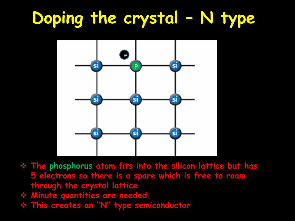
Doping the crystal – N type
The phosphorus atom fits into the silicon lattice but has 5 electrons so there is a spare which is free to roam through the crystal lattice
Minute quantities are needed. This creates an “N” type semiconductor
e
P

Doping the crystal – P type
If instead we dope the silicon with Boron, which has 3 electrons in the outer orbit we create an ABSENCE of electron or a HOLE which gets filled by stealing an electron from the adjacent atom
Holes appear to be positive charges and travel in the opposite direction to electrons!
e
B

The PN junction – a “forward biased” diode
Connect a battery across a PN
junction
When the negative end of the
circuit is connected to the N-
type layer and the positive
end is connected to the P-
type layer, electrons and
holes start moving across the
junction

The PN junction – a “reverse biased” diode
Reverse the battery across a
PN junction
When the positive end of the
circuit is connected to the N-
type layer and the negative
end is connected to the P-
type layer, there is no
movement of electrons and a
depletion layer is formed

Forward biased region
Apply enough reverse bias and junction breaks down
Reverse biased region.
Current flowing in a PN diode junction

Schematic physical diagram of a PN silicon junction diode

Germanium versus Silicon Parameter Germanium Silicon Comments
Depletion layer p.d. 0.15V 0.6V Germanium can be useful for low voltage applications.
Forward current A few milli-amperes
Tens of amperes Silicon much better for high current applications.
Reverse leakage current A few micro-amperes
A few nano-amperes
Germanium 1000 times more leaky than silicon.
Max. reverse voltage Volts Hundreds of volts Silicon is the only real choice for high voltage applications.
Temperature stability Poor Good Germanium more sensitive to temperature. Can be a problem or can be useful.
Junction capacitance Very low (point contact)
Comparatively high
This is a useful feature for high frequency use. Note: low capacitance silicon diodes are also available but still higher capacitance than point contact types.

Genesis of the Transistor
Every picture is worth 1000 words…
No love lost between these guys. Bardeen Shockley and Brattain in a 1948 shot at Bell labs
The transistor was invented in 1948 and patented by the three of them

Genesis of the Transistor
This was the example on which the 1948 patent rested
The semiconductor world really kicked off at this point
The semiconductor material used is Germanium
The three scientists were awarded a Nobel prize for their work
In fact there were earlier patents as early as 1925 but no physical device was ever constructed

A transistor is created by using three layers rather than the two
layers used in a diode. You can create either an NPN or a PNP
sandwich. A transistor can act as a switch or as an amplifier.
A transistor looks like two diodes back-to-back. You'd imagine that
no current could flow through a transistor because back-to-back
diodes would block current both ways. And this is true. However,
when you apply a small current to the centre layer of the sandwich,
a much larger current can flow through the sandwich as a whole.
This gives a transistor its switching or amplifying behaviour. A small
current can turn a larger current on and off.
What is a junction transistor - I?

What is a junction transistor - II? A Junction transistor is a three
terminal device
An signal current change in the base-
emitter circuit produces a (much)
larger change in the collector current
This is the principle of amplification
Maths-wise it is a bit more
complicated because unlike the old
valve triode (which the transistor
replaces) there is some feedback
between collector and base circuits

Early Transistors
Mullard grown junction transistor c. 1953
Not a great success The semiconductor material
used is Germanium
Mullard alloyed junction transistor c. 19541960
Glass encapsulated Low power Audio frequency
applications Filled with bouncing putty**!!
**65% dimethyl siloxane 17% silica 9% Thixatrol ST 4% polydimethylsiloxane, 1% decamethyl cyclopentasiloxane, 1% glycerine, and 1% titanium dioxide

More early Transistors
“The first germanium RF transistor”
Introduced 1956 Used (extensively) by me while
working for English Electric Guided Weapons division (now Bae)
Mullard’s first germanium power transistor
Also introduced in 1956 Typical of Philips “not invented
here” approach, using a non standard stud mounting

Silicon replaces Germanium
Mullard introduced silicon
transistors with all the
advantages of silicon in 1959
Glass in metal can construction
Still packed with bouncing
putty!
Still alloy-diffused transistors
and heavily manual
manufacturing processes

MOSFET Metal Oxide Silicon Field
Effect Transistor Theoretical cross sectional view Isometric view
Circuit symbols

Manufacturing techniques - I Given the perfectly grown crystal of silicon there was still much to do by
way of technology
In the early years there were many different manufacturing techniques
for the bipolar transistor
All strived to reduce costs; increase throughout; increase longevity of
devices and consistency of performance
Examples:
The grown junction
The mesa transistor
Alloy diffused transistor
The planar process
Use of epitaxial layer
UV based photolithographic processes
Ion deposition
Electron beam etching
X-ray lithography

Manufacturing techniques - II The semiconductor industry recruited many senior chemists; physicists;
metallurgists; photographers; statisticians and mechanical engineers
Manufacturing a “wafer” of individual transistors was only the first step
The back side of the wafer had to be coated in vacuo with am appprpriate
metral to form an adherent ohmic connection
All devices had to be tested with micro probes to weed out those devices
failing the specification
The wafer was then diced to produce each individual transistor die
The die was mounted onto a header, using the right alloy: (an incorrect
choice of alloy could lead to failure through the die either failing to be
wetted to the header or being poisoned by one of the constituent elements
Once successfully mounted, two remaining connections had to be made
between the die and the terminal posts in the header. The correct choice of
wire (gold or aluminium) and the bonding method (ultrasonic or
thermocompression) were essential

The first integrated circuit
Developed by Jack Kilby of Texas in 1958 A single transistor and supporting
components on a slice of germanium

Bigger and yet smaller
Moore’s Law. In 1965, Gordon Moore wrote that
the number of transistors in an IC had doubled
every year between 1958 and 1965 and that the
trend would continue for 10 years…
He was more than right. Moore’s law has continued
to apply for more than 47 years!
Processing speeds double every two years
Geometry gets smaller and smaller Currently we are
working towards a 23nM geometry

Bigger and yet smaller SSI. Early 60s. Small Scale Integration. Less than
100 transistors on a chip
MSI. Late 60s. Medium Scale Integration.
Hundreds of transistors on a chip
LSI. Early 80s. Large Scale Integration. Thousands
of transistors on a chip
VLSI. Very Large Scale Integration. Initially
10,000+ transistors on a chip. Now with the Central
Processor chip we have 100,000 – 1,000,000+
transistors on a chip (10,000,000??)

Log
(Tra
nsisto
r co
unt)
Curve shows a transistor count doubling every two years
Moore’s Law - Microprocessor Transistor Counts 1971-2011

Inside a computer CPU The brain of your PC

The bigger picture

And now or something completely different
Gallium Arsenide

Gallium Arsenide – a band III band V semiconductor
Gallium arsenide is a crystal – just like Silicon or Germanium but is
comprised of alternate atoms of Gallium and Arsenic
Advantages over Silicon:
Higher saturated electron velocity and higher mobility so can
function at frequencies above 250GHz
Lower noise
Higher specific resistivity
Orders of magnitude harder than silicon when exposed to
radiation
Several times faster than silicon
Direct band gap material so can be tailored to emit light
Can be used to fabricate GUNN diodes for Doppler radar devices

Gallium Arsenide – a band III band V semiconductor
No such thing as a free lunch though…
Disadvantages compared with Silicon:
× Neither abundant nor cheap
× Highly toxic – disposal problems
× Extremely brittle
× Poor thermal conductor
× No ability to create a passivating oxide like SiO2
× Low hole mobility so cannot be used for CMOS
× Much higher power consumption than silicon

Light emitting diodes (LED) - I
An LED is simply a P-N junction that is forward biased
LEDs are fabricated from complex semiconductors (like Gallium
Phosphide; Gallium Arsenide Phosphide; Gallium Arsenide; Gallium
Nitride)
When electrons cross the junction from the n- to the p-type
material, the electron-hole recombination process produces some
photons in the Infra Red or Visible spectrum in a process called
electroluminescence.
GaAs; GaAsP; GaP; GaN

Light emitting diodes (LED) - II
1962 The first practical LED
1960s Use of low intensity red LEDs for indicators and 7 segment displays
1970s 7 segment LEDs displaced by increasing availability of LCD displays
1980s Green and yellow LEDs appear. Crystal defects mean that light
outputs are still low
1990s Gallium Nitride LED gives brilliant and efficient blue light. Partial
conversion with phosphor coating allows conversion to white light. White
LEDs in production in 1993
2000s Higher and whiter (Warm white; white and Cool white available)
LEDs – the timeline

Then there are Solar Panels

U3A Science & Technology
Semiconductors - The End