TX Digital VGA - Renesas Electronics
28
T © 2016 Integrated Device Technology, Inc 1 November 9, 2016 TX Digital VGA 2100 MHz to 2950 MHz F1456 Datasheet Description The F1456 is a High Gain / High Linearity 2100 MHz to 2950 MHz TX Digital Variable Gain Amplifier used in transmitter applications. The F1456 TX DVGA provides 32.1 dB maximum gain with +38 dBm OIP3 and 3.9 dB noise figure. Up to 31.5 dB gain control is achieved using the combination of a digital step attenuator (DSA) and a KLIN TM RF Digital Gain Amplifier. This device uses a single 5 V supply and 215 mA of ICC. This device is packaged in a 6 mm x 6 mm, 28-pin QFN with 50 Ω single-ended RF input and RF output impedances for ease of integration into the signal-path. Competitive Advantage In typical Base Stations, RF VGAs are used in the TX traffic paths to drive the transmit power amplifier. The F1456 TX DVGA offers very high reliability due to its construction from a monolithic silicon die in a QFN package. The F1456 is configured to provide an optimum balance of noise and linearity performance consisting of a KLIN TM RF amplifier, digital step attenuator (DSA) and a PA driver amplifier. The KLIN TM amplifier maintains the OIP3 and output P1dB performance over an extended attenuation range when compared to competitive devices. Typical Applications Multi-mode, Multi-carrier Transmitters WiMAX and LTE Base Stations UMTS/WCDMA 3G Base Stations PHS/PAS Base Stations Public Safety Infrastructure Features Broadband 2100 MHz to 2950 MHz 32.1 dB max gain 3.9 dB NF @ max gain (2650 MHz) 31.5 dB total gain control range, 0.5 dB step < 2 dB overshoot between gain transitions Maintains flat +21.5 dBm OP1dB for more than 13 dB gain adjustment range Maintains flat +38 dBm OIP3 for more than 15 dB gain adjustment range SPI interface for DSA control Single 5 V supply voltage ICC = 215 mA Up to +105 °C TCASE operating temperature 50 Ω input and output impedance Standby mode for power savings Pin compatible 700 MHz and 2100 MHz versions 6 mm x 6 mm, 28-pin QFN package Block Diagram Figure 1. Block Diagram 6 mm x 6 mm 28-pin /STBY Bias DSA Digital CTL PA Driver K LIN TM DVGA RF IN 3 RF OUT SPI & Decoder KLIN Constant High Linearity TM
Transcript of TX Digital VGA - Renesas Electronics

T
© 2016 Integrated Device Technology, Inc 1 November 9, 2016
TX Digital VGA
2100 MHz to 2950 MHz
F1456
Datasheet
Description
The F1456 is a High Gain / High Linearity 2100 MHz to 2950 MHz TX Digital Variable Gain Amplifier used in transmitter applications.
The F1456 TX DVGA provides 32.1 dB maximum gain with +38 dBm OIP3 and 3.9 dB noise figure. Up to 31.5 dB gain control is achieved using the combination of a digital step attenuator (DSA) and a KLIN
TM RF Digital Gain Amplifier. This device uses a single 5 V supply and 215 mA of ICC.
This device is packaged in a 6 mm x 6 mm, 28-pin QFN with 50 Ω single-ended RF input and RF output impedances for ease of integration into the signal-path.
Competitive Advantage
In typical Base Stations, RF VGAs are used in the TX traffic paths to drive the transmit power amplifier. The F1456 TX DVGA offers very high reliability due to its construction from a monolithic silicon die in a QFN package. The F1456 is configured to provide an optimum balance of noise and linearity performance consisting of a KLIN
TM RF amplifier, digital step attenuator (DSA) and a PA driver amplifier. The KLIN
TM amplifier maintains the OIP3 and output P1dB performance over an extended attenuation range when compared to competitive devices.
Typical Applications
Multi-mode, Multi-carrier Transmitters
WiMAX and LTE Base Stations
UMTS/WCDMA 3G Base Stations
PHS/PAS Base Stations
Public Safety Infrastructure
Features
Broadband 2100 MHz to 2950 MHz
32.1 dB max gain
3.9 dB NF @ max gain (2650 MHz)
31.5 dB total gain control range, 0.5 dB step
< 2 dB overshoot between gain transitions
Maintains flat +21.5 dBm OP1dB for more than 13 dB gain adjustment range
Maintains flat +38 dBm OIP3 for more than 15 dB gain adjustment range
SPI interface for DSA control
Single 5 V supply voltage
ICC = 215 mA
Up to +105 °C TCASE operating temperature
50 Ω input and output impedance
Standby mode for power savings
Pin compatible 700 MHz and 2100 MHz versions
6 mm x 6 mm, 28-pin QFN package
Block Diagram
Figure 1. Block Diagram
6 mm x 6 mm 28-pin
/STBY
Bias
DSA
Digital CTL
PA DriverKLINTM DVGA
RF IN
3
RF OUT
SPI & Decoder
KLINConstant
High LinearityTM

F1456 Datasheet
© 2016 Integrated Device Technology, Inc 2 November 9, 2016
Pin Assignments
Figure 2. Pin Assignments for 6 mm x 6 mm x 0.9 mm QFN Package – Top View
CLK
CSb
7
6
5
4
3
2
1
DATA
RSET
GND
GND
RFIN
NC
GND
15
16
17
18
19
20
21
NC
NC
GND
GND
RFOUT
NC
NC
14
13
12
11
1098
NC
NC
/S
TB
Y
NC
NC
F1456
Exposed Pad(GND)
NC
VC
C
22
23
24
25
26
27
28
GN
D
NC
NC
NC
GN
D

F1456 Datasheet
© 2016 Integrated Device Technology, Inc 3 November 9, 2016
Pin Descriptions
Table 1. Pin Descriptions
Number Name Description
1 CSb Chip Select Input: 1.8 V or 3.3 V logic compatible.
2 DATA Data Input: 1.8 V or 3.3 V logic compatible.
3 CLK Clock Input: 1.8 V or 3.3 V logic compatible.
4 [a] RSET Connect 2.2 kΩ external resistor to GND to set amplifier bias.
5, 7, 15, 17, 21, 23, 27
GND Pins internally tied to exposed paddle. Connect to ground on PCB.
6 RFIN RF input internally matched to 50 Ω. Must use external DC block.
8, 9, 10, 11, 12, 13, 18, 19, 20, 22, 24, 25, 26
NC No internal connection. These pins can be left unconnected, voltage applied, or connected to ground (recommended).
14 /STBY Standby pin. Device will be placed in standby mode when pin 14 is set to a logic low or when pin 14 is left floating (pulled low via internal high impedance to GND). In standby mode, SPI circuitry is still active. With a logic high applied to pin 14 the part is set to full operation mode.
16 RFOUT RF output internally matched to 50 Ω. Must use external DC block.
28 VCC 5 V Power Supply. Connect to Vcc and use bypass capacitors as close to the pin as possible.
— EP Exposed Pad. Internally connected to GND. Solder this exposed pad to a PCB pad that uses multiple ground vias to provide heat transfer out of the device into the PCB ground planes. These multiple ground vias are also required to achieve the noted RF performance.
a. External resistor on pin 4 used to optimize the overall device for DC current and linearity performance across the entire frequency band.

F1456 Datasheet
© 2016 Integrated Device Technology, Inc 4 November 9, 2016
Absolute Maximum Ratings
Stresses above those listed below may cause permanent damage to the device. Functional operation of the device at these or any other conditions above those indicated in the operational section of this specification is not implied. Exposure to absolute maximum rating conditions for extended periods may affect device reliability.
Table 2. Absolute Maximum Ratings
Parameter Symbol Minimum Maximum Units
Vcc to GND VCC -0.5 5.5 V
DATA, CSb, CLK, /STBY VCntrl -0.5 VCC V
RSET IRSET +1.5 mA
RFIN externally applied DC voltage VRFIN +1.4 +3.6 V
RFOUT externally applied DC voltage VRFOUT VCC - 0.15 VCC + 0.15 V
RF Input Power (RFIN) applied for 24 hours max. [a] Pmax_in +12 dBm
RF Output Power (RFOUT) present for 24 hours maximum [a]
Pmax_out +26 dBm
Continuous Power Dissipation Pdiss 1.75 W
Junction Temperature Tj 150 °C
Storage Temperature Range Tst -65 150 °C
Lead Temperature (soldering, 10s) 260 °C
ElectroStatic Discharge – HBM (JEDEC/ESDA JS-001-2012)
2000
(Class 2) V
ElectroStatic Discharge – CDM (JEDEC 22-C101F)
1000
(Class C3) V
a. Exposure to these maximum RF levels can result in significantly higher Icc current draw due to overdriving the amplifier stages.

F1456 Datasheet
© 2016 Integrated Device Technology, Inc 5 November 9, 2016
Recommended Operating Conditions
Table 3. Recommended Operating Conditions
Parameter Symbol Condition Minimum Typical Maximum Units
Power Supply Voltage VCC 4.75 5.25 V
Operating Temperature Range TCASE Exposed Paddle -40 +105 °C
RF Frequency Range [a] FRF High Linearity Bandwidth 2100 2700
MHz Extended band for DPD 2700 2950
Maximum Operating Average RF Output Power
ZS = ZL = 50 14 dBm
RFIN Port Impedance ZRFI Single Ended 50
RFOUT Port Impedance ZRFO Single Ended 50
a. Device linearity is optimized over the range from 2100 MHz to 2700 MHz. Gain flatness is optimized up to 2950 MHz to account for
systems with extended DPD bandwidth requirements.
F1456 Datasheet
© 2016 Integrated Device Technology, Inc 6 November 9, 2016
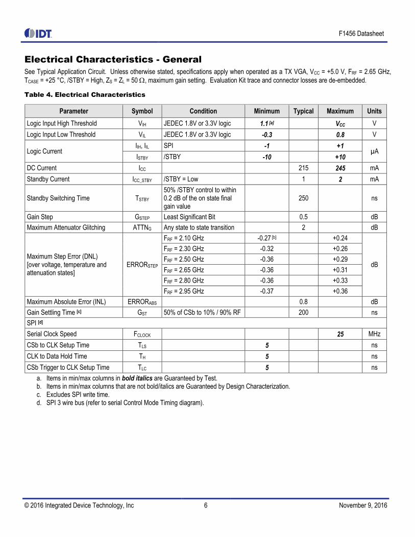
Electrical Characteristics - General
See Typical Application Circuit. Unless otherwise stated, specifications apply when operated as a TX VGA, VCC = +5.0 V, FRF = 2.65 GHz,
TCASE = +25 °C, /STBY = High, ZS = ZL = 50 , maximum gain setting. Evaluation Kit trace and connector losses are de-embedded.
Table 4. Electrical Characteristics
Parameter Symbol Condition Minimum Typical Maximum Units
Logic Input High Threshold VIH JEDEC 1.8V or 3.3V logic 1.1 [a] VCC V
Logic Input Low Threshold VIL JEDEC 1.8V or 3.3V logic -0.3 0.8 V
Logic Current IIH, IIL SPI -1 +1
µA ISTBY /STBY -10 +10
DC Current ICC 215 245 mA
Standby Current ICC_STBY /STBY = Low 1 2 mA
Standby Switching Time TSTBY 50% /STBY control to within 0.2 dB of the on state final gain value
250 ns
Gain Step GSTEP Least Significant Bit 0.5 dB
Maximum Attenuator Glitching ATTNG Any state to state transition 2 dB
Maximum Step Error (DNL) [over voltage, temperature and attenuation states]
ERRORSTEP
FRF = 2.10 GHz -0.27 [b] +0.24
dB
FRF = 2.30 GHz -0.32 +0.26
FRF = 2.50 GHz -0.36 +0.29
FRF = 2.65 GHz -0.36 +0.31
FRF = 2.80 GHz -0.36 +0.33
FRF = 2.95 GHz -0.37 +0.36
Maximum Absolute Error (INL) ERRORABS 0.8 dB
Gain Settling Time [c] GST 50% of CSb to 10% / 90% RF 200 ns
SPI [d]
Serial Clock Speed FCLOCK 25 MHz
CSb to CLK Setup Time TLS 5 ns
CLK to Data Hold Time TH 5 ns
CSb Trigger to CLK Setup Time TLC 5 ns
a. Items in min/max columns in bold italics are Guaranteed by Test. b. Items in min/max columns that are not bold/italics are Guaranteed by Design Characterization. c. Excludes SPI write time. d. SPI 3 wire bus (refer to serial Control Mode Timing diagram).

F1456 Datasheet
© 2016 Integrated Device Technology, Inc 7 November 9, 2016
Electrical Characteristics - RF
See Typical Application Circuit. Unless otherwise stated, specifications apply when operated as a TX VGA, VCC = +5.0 V, FRF = 2.65 GHz,
TCASE = +25 °C, /STBY = High, ZS = ZL = 50 , maximum gain setting. Evaluation Kit trace and connector losses are de-embedded.
Table 5. Electrical Characteristics
Parameter Symbol Condition Minimum Typical Maximum Units
RF Input Return Loss RLRFIN 12 dB
RF Output Return Loss RLRFOUT 12 dB
Gain - Max Gain Setting GMAX 30.6 32.1 33.6 dB
Gain - Min Gain Setting GMIN Max attenuation -1.5 0 1.5 dB
Gain Flatness [c] GFLAT FRF = 2100 MHz to 2700 MHz any 400 MHz BW
0.5 dB
Noise Figure NF
0 dB attenuation 3.9
dB
10 dB attenuation 5.9
20 dB attenuation 10.9
29.5 dB attenuation 19.5
31.5 dB attenuation 21.5
Output Third Order Intercept Point OIP3
0 dB attenuation Pout = +7 dBm / tone 5 MHz tone separation
41.9
dBm
6 dB attenuation Pin = -21 dBm / tone 5 MHz tone separation
45.4
10 dB attenuation Pin = -21 dBm / tone 5 MHz tone separation
35.5 43.6
20 dB attenuation Pin = -21 dBm / tone 5 MHz tone separation
36.1
29.5 dB attenuation Pin = -21 dBm / tone 5 MHz tone separation
27.4
31.5 dB attenuation Pin = -21 dBm / tone 5 MHz tone separation
25.7
Output 1dB Compression Point OP1dB
0 dB attenuation 21.9
dBm 0 dB attenuation, TCASE = +105 °C
21.4
6 dB attenuation 20.9 21.9
a. Items in min/max columns in bold italics are Guaranteed by Test. b. Items in min/max columns that are not bold/italics are Guaranteed by Design Characterization. c. Includes a positive slope feature over the noted RF range to compensate for typical system roll-off.

F1456 Datasheet
© 2016 Integrated Device Technology, Inc 8 November 9, 2016
Thermal Characteristics
Table 6. Package Thermal Characteristics
Parameter Symbol Value Units
Junction to Ambient Thermal Resistance. θJA 40 °C/W
Junction to Case Thermal Resistance. (Case is defined as the exposed paddle)
θJC 4 °C/W
Moisture Sensitivity Rating (Per J-STD-020) MSL 1
Typical Operating Conditions (TOC)
Unless otherwise stated the typical operating graphs were measured under the following conditions:
Vcc = 5.0 V
ZL = ZS = 50 Ohms Single Ended
FRF = 2.65 GHz
TCASE = +25 °C
/STBY = High
5 MHz Tone Spacing
Gain setting = Maximum Gain
All temperatures are referenced to the exposed paddle
ACLR measurements used with a Basic LTE FDD Downlink 20 MHz TM1.2 Test signal
EVM measurements used with a Basic LTE FDD Downlink 20 MHz TM3.1 Test signal
Note TN1: Atten ≤ 4 dB Fixed Pout = 7 dBm per waveform or per tone, Atten > 4 dB Fixed Pin = -21 dBm per waveform or per tone
Note TN2: Atten ≤ 7 dB Fixed Pout = 10.5 dBm per waveform or per tone, Atten > 7 dB Fixed Pin = -14.5 dBm per waveform or per tone
Evaluation Kit traces and connector losses are de-embedded

F1456 Datasheet
© 2016 Integrated Device Technology, Inc 9 November 9, 2016
Typical Performance Characteristics
Figure 3. Maximum Gain vs. Frequency over
Temp and Voltage [Attn = 0.0 dB]
Figure 4. Reverse Isolation vs. Frequency over
Temp and Voltage [Attn = 0.0 dB]
Figure 5. Input Return Loss vs. Frequency over
Temp and Voltage [Attn = 0.0 dB]
Figure 6. Output Return Loss vs. Frequency
over Temp and Voltage [Attn = 0.0 dB]
Figure 7. Stability vs. Frequency over
Temperature and Voltage [Attn = 0.0 dB]
Figure 8. EvKit Insertion Loss vs. Frequency
over Temperature
25
26
27
28
29
30
31
32
33
34
35
1.0 1.5 2.0 2.5 3.0 3.5 4.0
Ga
in (
dB
)
Frequency (GHz)
-40 C / +4.75 V -40 C / +5.00 V -40 C / +5.25 V
+25 C / +4.75 V +25 C / +5.00 V +25 C / +5.25 V
+105 C / +4.75 V +105 C / +5.00 V +105 C / +5.25 V
-60
-55
-50
-45
-40
-35
-30
-25
-20
-15
-10
-5
0
1.0 1.5 2.0 2.5 3.0 3.5 4.0
Re
ve
rse
Iso
lati
on
(d
B)
Frequency (GHz)
-40 C / +4.75 V -40 C / +5.00 V -40 C / +5.25 V
+25 C / +4.75 V +25 C / +5.00 V +25 C / +5.25 V
+105 C / +4.75 V +105 C / +5.00 V +105 C / +5.25 V
-30
-25
-20
-15
-10
-5
0
1.0 1.5 2.0 2.5 3.0 3.5 4.0
Ma
tch
(d
B)
Frequency (GHz)
-40 C / +4.75 V -40 C / +5.00 V -40 C / +5.25 V
+25 C / +4.75 V +25 C / +5.00 V +25 C / +5.25 V
+105 C / +4.75 V +105 C / +5.00 V +105 C / +5.25 V
-30
-25
-20
-15
-10
-5
0
1.0 1.5 2.0 2.5 3.0 3.5 4.0
Ma
tch
(d
B)
Frequency (GHz)
-40 C / +4.75 V -40 C / +5.00 V -40 C / +5.25 V
+25 C / +4.75 V +25 C / +5.00 V +25 C / +5.25 V
+105 C / +4.75 V +105 C / +5.00 V +105 C / +5.25 V
0
1
2
3
4
5
6
7
8
9
10
0 1 2 3 4 5 6 7 8 9
K F
acto
r
Frequency (GHz)
-40 C / +4.75 V -40 C / +5.00 V -40 C / +5.25 V
+25 C / +4.75 V +25 C / +5.00 V +25 C / +5.25 V
+105 C / +4.75 V +105 C / +5.00 V +105 C / +5.25 V
-3.0
-2.5
-2.0
-1.5
-1.0
-0.5
0.0
0 1 2 3 4 5 6 7 8 9
Inse
rtio
n L
oss (
dB
)
Frequency (GHz)
-40 C
+25 C
+105 C
F1456 Datasheet
© 2016 Integrated Device Technology, Inc 10 November 9, 2016
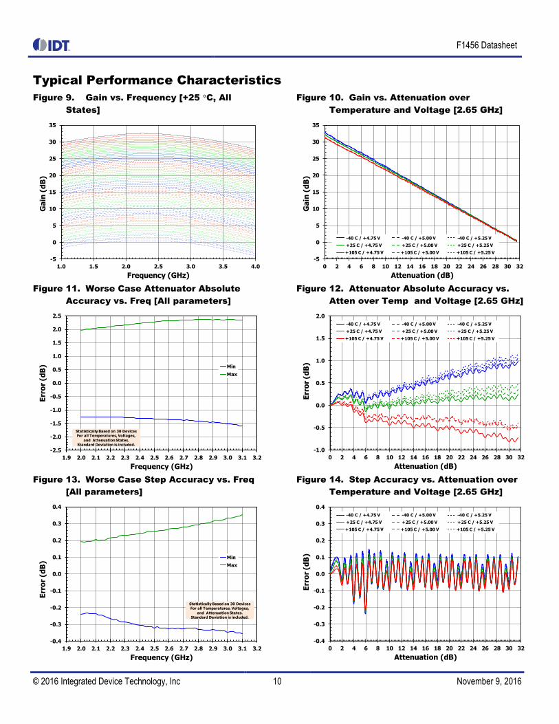
Typical Performance Characteristics
Figure 9. Gain vs. Frequency [+25 °C, All
States]
Figure 10. Gain vs. Attenuation over
Temperature and Voltage [2.65 GHz]
Figure 11. Worse Case Attenuator Absolute
Accuracy vs. Freq [All parameters]
Figure 12. Attenuator Absolute Accuracy vs.
Atten over Temp and Voltage [2.65 GHz]
Figure 13. Worse Case Step Accuracy vs. Freq
[All parameters]
Figure 14. Step Accuracy vs. Attenuation over
Temperature and Voltage [2.65 GHz]
-5
0
5
10
15
20
25
30
35
1.0 1.5 2.0 2.5 3.0 3.5 4.0
Ga
in (
dB
)
Frequency (GHz)
-5
0
5
10
15
20
25
30
35
0 2 4 6 8 10 12 14 16 18 20 22 24 26 28 30 32
Ga
in (
dB
)
Attenuation (dB)
-40 C / +4.75 V -40 C / +5.00 V -40 C / +5.25 V
+25 C / +4.75 V +25 C / +5.00 V +25 C / +5.25 V
+105 C / +4.75 V +105 C / +5.00 V +105 C / +5.25 V
-2.5
-2.0
-1.5
-1.0
-0.5
0.0
0.5
1.0
1.5
2.0
2.5
1.9 2.0 2.1 2.2 2.3 2.4 2.5 2.6 2.7 2.8 2.9 3.0 3.1 3.2
Err
or
(dB
)
Frequency (GHz)
Min
Max
Statistically Based on 30 DevicesFor all Temperatures, Voltages,
and Attenuation States. Standard Deviation is included.
-1.0
-0.5
0.0
0.5
1.0
1.5
2.0
0 2 4 6 8 10 12 14 16 18 20 22 24 26 28 30 32
Err
or
(dB
)
Attenuation (dB)
-40 C / +4.75 V -40 C / +5.00 V -40 C / +5.25 V
+25 C / +4.75 V +25 C / +5.00 V +25 C / +5.25 V
+105 C / +4.75 V +105 C / +5.00 V +105 C / +5.25 V
-0.4
-0.3
-0.2
-0.1
0.0
0.1
0.2
0.3
0.4
1.9 2.0 2.1 2.2 2.3 2.4 2.5 2.6 2.7 2.8 2.9 3.0 3.1 3.2
Err
or
(dB
)
Frequency (GHz)
Min
Max
Statistically Based on 30 DevicesFor all Temperatures, Voltages,
and Attenuation States. Standard Deviation is included.
-0.4
-0.3
-0.2
-0.1
0.0
0.1
0.2
0.3
0.4
0 2 4 6 8 10 12 14 16 18 20 22 24 26 28 30 32
Err
or
(dB
)
Attenuation (dB)
-40 C / +4.75 V -40 C / +5.00 V -40 C / +5.25 V
+25 C / +4.75 V +25 C / +5.00 V +25 C / +5.25 V
+105 C / +4.75 V +105 C / +5.00 V +105 C / +5.25 V

F1456 Datasheet
© 2016 Integrated Device Technology, Inc 11 November 9, 2016
Typical Performance Characteristics
Figure 15. Input Return Loss vs. Frequency
[+25 °C, All states]
Figure 16. Input Return Loss vs. Attenuation
over Temperature and Voltage [2.65 GHz]
Figure 17. Output Return Loss vs. Frequency
[+25 °C, All states]
Figure 18. Output Return Loss vs. Attenuation
over Temperature and Voltage [2.65 GHz]
Figure 19. Reverse Isolation vs. Frequency
[+25 °C, All states]
Figure 20. Reverse Isolation vs. Attenuation
over Temperature and Voltage [2.65 GHz]
-30
-25
-20
-15
-10
-5
0
1.0 1.5 2.0 2.5 3.0 3.5 4.0
Ma
tch
(d
B)
Frequency (GHz)
-30
-25
-20
-15
-10
-5
0
0 2 4 6 8 10 12 14 16 18 20 22 24 26 28 30 32
Ma
tch
(d
B)
Attenuation (dB)
-40 C / +4.75 V -40 C / +5.00 V -40 C / +5.25 V
+25 C / +4.75 V +25 C / +5.00 V +25 C / +5.25 V
+105 C / +4.75 V +105 C / +5.00 V +105 C / +5.25 V
-30
-25
-20
-15
-10
-5
0
1.0 1.5 2.0 2.5 3.0 3.5 4.0
Ma
tch
(d
B)
Frequency (GHz)
-30
-25
-20
-15
-10
-5
0
0 2 4 6 8 10 12 14 16 18 20 22 24 26 28 30 32
Ma
tch
(d
B)
Attenuation (dB)
-40 C / +4.75 V -40 C / +5.00 V -40 C / +5.25 V
+25 C / +4.75 V +25 C / +5.00 V +25 C / +5.25 V
+105 C / +4.75 V +105 C / +5.00 V +105 C / +5.25 V
-70
-65
-60
-55
-50
-45
-40
-35
-30
-25
-20
1.0 1.5 2.0 2.5 3.0 3.5 4.0
Re
ve
rse
Iso
lati
on
(d
B)
Frequency (GHz)
-70
-65
-60
-55
-50
-45
-40
-35
-30
-25
-20
-15
-10
-5
0
0 2 4 6 8 10 12 14 16 18 20 22 24 26 28 30 32
Re
ve
rse
Iso
lati
on
(d
B)
Attenuation (dB)
-40 C / +4.75 V -40 C / +5.00 V -40 C / +5.25 V
+25 C / +4.75 V +25 C / +5.00 V +25 C / +5.25 V
+105 C / +4.75 V +105 C / +5.00 V +105 C / +5.25 V
F1456 Datasheet
© 2016 Integrated Device Technology, Inc 12 November 9, 2016
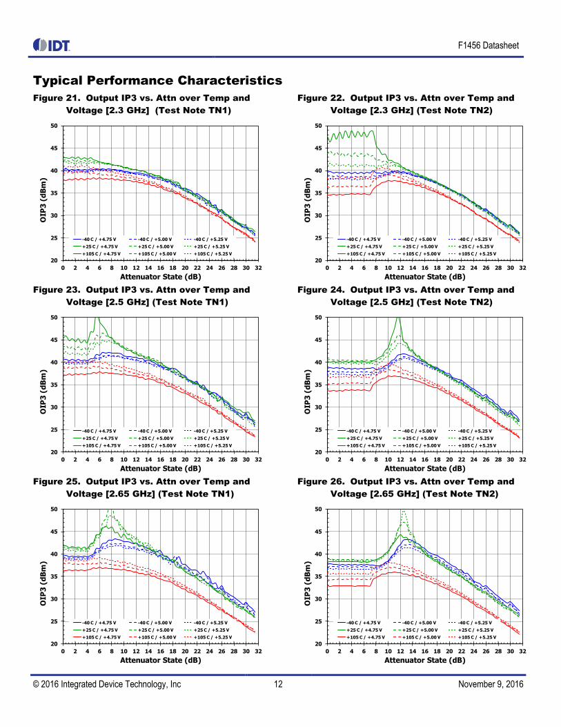
Typical Performance Characteristics
Figure 21. Output IP3 vs. Attn over Temp and
Voltage [2.3 GHz] (Test Note TN1)
Figure 22. Output IP3 vs. Attn over Temp and
Voltage [2.3 GHz] (Test Note TN2)
Figure 23. Output IP3 vs. Attn over Temp and
Voltage [2.5 GHz] (Test Note TN1)
Figure 24. Output IP3 vs. Attn over Temp and
Voltage [2.5 GHz] (Test Note TN2)
Figure 25. Output IP3 vs. Attn over Temp and
Voltage [2.65 GHz] (Test Note TN1)
Figure 26. Output IP3 vs. Attn over Temp and
Voltage [2.65 GHz] (Test Note TN2)
20
25
30
35
40
45
50
0 2 4 6 8 10 12 14 16 18 20 22 24 26 28 30 32
OIP
3 (
dB
m)
Attenuator State (dB)
-40 C / +4.75 V -40 C / +5.00 V -40 C / +5.25 V
+25 C / +4.75 V +25 C / +5.00 V +25 C / +5.25 V
+105 C / +4.75 V +105 C / +5.00 V +105 C / +5.25 V
20
25
30
35
40
45
50
0 2 4 6 8 10 12 14 16 18 20 22 24 26 28 30 32
OIP
3 (
dB
m)
Attenuator State (dB)
-40 C / +4.75 V -40 C / +5.00 V -40 C / +5.25 V
+25 C / +4.75 V +25 C / +5.00 V +25 C / +5.25 V
+105 C / +4.75 V +105 C / +5.00 V +105 C / +5.25 V
20
25
30
35
40
45
50
0 2 4 6 8 10 12 14 16 18 20 22 24 26 28 30 32
OIP
3 (
dB
m)
Attenuator State (dB)
-40 C / +4.75 V -40 C / +5.00 V -40 C / +5.25 V
+25 C / +4.75 V +25 C / +5.00 V +25 C / +5.25 V
+105 C / +4.75 V +105 C / +5.00 V +105 C / +5.25 V
20
25
30
35
40
45
50
0 2 4 6 8 10 12 14 16 18 20 22 24 26 28 30 32
OIP
3 (
dB
m)
Attenuator State (dB)
-40 C / +4.75 V -40 C / +5.00 V -40 C / +5.25 V
+25 C / +4.75 V +25 C / +5.00 V +25 C / +5.25 V
+105 C / +4.75 V +105 C / +5.00 V +105 C / +5.25 V
20
25
30
35
40
45
50
0 2 4 6 8 10 12 14 16 18 20 22 24 26 28 30 32
OIP
3 (
dB
m)
Attenuator State (dB)
-40 C / +4.75 V -40 C / +5.00 V -40 C / +5.25 V
+25 C / +4.75 V +25 C / +5.00 V +25 C / +5.25 V
+105 C / +4.75 V +105 C / +5.00 V +105 C / +5.25 V
20
25
30
35
40
45
50
0 2 4 6 8 10 12 14 16 18 20 22 24 26 28 30 32
OIP
3 (
dB
m)
Attenuator State (dB)
-40 C / +4.75 V -40 C / +5.00 V -40 C / +5.25 V
+25 C / +4.75 V +25 C / +5.00 V +25 C / +5.25 V
+105 C / +4.75 V +105 C / +5.00 V +105 C / +5.25 V

F1456 Datasheet
© 2016 Integrated Device Technology, Inc 13 November 9, 2016
Typical Performance Characteristics
Figure 27. Output IP3 vs. Frequency over
Temperature and Voltage [Attn = 0.0 dB]
Figure 28. Output P1dB vs. Attenuation over
Temperature and Voltage [2.3 GHz]
Figure 29. Output P1dB vs. Frequency over
Temp and Voltage [Attn = 0.0 dB]
Figure 30. Output P1dB vs. Attenuation over
Temp and Voltage [2.5 GHz]
Figure 31. Output P1dB vs. Attenuation over
Temp and Voltage [2.65 GHz]
30
32
34
36
38
40
42
44
46
48
50
2.0 2.1 2.2 2.3 2.4 2.5 2.6 2.7 2.8 2.9 3.0
OIP
3 (
dB
m)
Frequency (GHz)
-40 C / +4.75 V -40 C / +5.00 V -40 C / +5.25 V
+25 C / +4.75 V +25 C / +5.00 V +25 C / +5.25 V
+105 C / +4.75 V +105 C / +5.00 V +105 C / +5.25 V
15
16
17
18
19
20
21
22
23
24
25
0 1 2 3 4 5 6 7 8 9
Ou
tpu
t P
1d
B (
dB
m)
Attenuation State (dB)
-40 C / +4.75 V / -40 C / +5.00 V / -40 C / +5.25 V /
+25 C / +4.75 V / +25 C / +5.00 V / +25 C / +5.25 V /
+105 C / +4.75 V / +105 C / +5.00 V / +105 C / +5.25 V /
15
16
17
18
19
20
21
22
23
24
25
2.0 2.1 2.2 2.3 2.4 2.5 2.6 2.7 2.8 2.9 3.0
Ou
tpu
t P
1d
B (
dB
m)
Frequency (GHz)
-40 C / +4.75 V -40 C / +5.00 V -40 C / +5.25 V
+25 C / +4.75 V +25 C / +5.00 V +25 C / +5.25 V
+105 C / +4.75 V +105 C / +5.00 V +105 C / +5.25 V
15
16
17
18
19
20
21
22
23
24
25
0 1 2 3 4 5 6 7 8 9
Ou
tpu
t P
1d
B (
dB
m)
Attenuation State (dB)
-40 C / +4.75 V / -40 C / +5.00 V / -40 C / +5.25 V /
+25 C / +4.75 V / +25 C / +5.00 V / +25 C / +5.25 V /
+105 C / +4.75 V / +105 C / +5.00 V / +105 C / +5.25 V /
15
16
17
18
19
20
21
22
23
24
25
0 1 2 3 4 5 6 7 8 9
Ou
tpu
t P
1d
B (
dB
m)
Attenuation State (dB)
-40 C / +4.75 V / -40 C / +5.00 V / -40 C / +5.25 V /
+25 C / +4.75 V / +25 C / +5.00 V / +25 C / +5.25 V /
+105 C / +4.75 V / +105 C / +5.00 V / +105 C / +5.25 V /

F1456 Datasheet
© 2016 Integrated Device Technology, Inc 14 November 9, 2016
Typical Performance Characteristics
Figure 32. Gain Compression vs. Pout over
Temperature and Voltage [2.3 GHz]
Figure 33. Phase Compression vs. Pout over
Temperature and Voltage [2.3 GHz]
Figure 34. Gain Compression vs. Pout over
Temperature and Voltage [2.5 GHz]
Figure 35. Phase Compression vs. Pout over
Temperature and Voltage [2.5 GHz]
Figure 36. Gain Compression vs. Pout over
Temperature and Voltage [2.65 GHz]
Figure 37. Phase Compression vs. Pout over
Temperature and Voltage [2.65 GHz]
-2.0
-1.5
-1.0
-0.5
0.0
0.5
12 13 14 15 16 17 18 19 20 21 22 23 24 25
Po
we
r C
om
pre
ssio
n (
dB
)
Output Power (dBm)
-40 C / +4.75 V -40 C / +5.00 V -40 C / +5.25 V
+25 C / +4.75 V +25 C / +5.00 V +25 C / +5.25 V
+105 C / +4.75 V +105 C / +5.00 V +105 C / +5.25 V
-25
-20
-15
-10
-5
0
5
12 13 14 15 16 17 18 19 20 21 22 23 24 25
Ph
ase
Co
mp
ressio
n (
de
gre
es)
Output Power (dBm)
-40 C / +4.75 V -40 C / +5.00 V -40 C / +5.25 V
+25 C / +4.75 V +25 C / +5.00 V +25 C / +5.25 V
+105 C / +4.75 V +105 C / +5.00 V +105 C / +5.25 V

F1456 Datasheet
© 2016 Integrated Device Technology, Inc 15 November 9, 2016
Typical Performance Characteristics
Figure 38. Noise Figure vs. Frequency over
Temperature and Voltage [Attn = 0.0 dB]
Figure 39. Noise Figure vs. Attenuation over
Temperature and Voltage [2.3 GHz]
Figure 40. Noise Figure vs. Attenuation over
Temperature and Voltage [2.5 GHz]
Figure 41. Noise Figure vs. Attenuation over
Temperature and Voltage [2.65 GHz]
0
1
2
3
4
5
6
2.0 2.1 2.2 2.3 2.4 2.5 2.6 2.7 2.8 2.9 3.0
No
ise
Fig
ure
(d
B)
Frequency (GHz)
-40 C / +4.75 V -40 C / +5.00 V -40 C / +5.25 V
+25 C / +4.75 V +25 C / +5.00 V +25 C / +5.25 V
+105 C / +4.75 V +105 C / +5.00 V +105 C / +5.25 V
0
5
10
15
20
25
0 2 4 6 8 10 12 14 16 18 20 22 24 26 28 30 32
No
ise
Fig
ure
(d
B)
Attenuation State (dB)
-40 C / +4.75 V -40 C / +5.00 V -40 C / +5.25 V
+25 C / +4.75 V +25 C / +5.00 V +25 C / +5.25 V
+105 C / +4.75 V +105 C / +5.00 V +105 C / +5.25 V
0
5
10
15
20
25
0 2 4 6 8 10 12 14 16 18 20 22 24 26 28 30 32
No
ise
Fig
ure
(d
B)
Attenuation State (dB)
-40 C / +4.75 V -40 C / +5.00 V -40 C / +5.25 V
+25 C / +4.75 V +25 C / +5.00 V +25 C / +5.25 V
+105 C / +4.75 V +105 C / +5.00 V +105 C / +5.25 V
0
5
10
15
20
25
0 2 4 6 8 10 12 14 16 18 20 22 24 26 28 30 32
No
ise
Fig
ure
(d
B)
Attenuation State (dB)
-40 C / +4.75 V -40 C / +5.00 V -40 C / +5.25 V
+25 C / +4.75 V +25 C / +5.00 V +25 C / +5.25 V
+105 C / +4.75 V +105 C / +5.00 V +105 C / +5.25 V

F1456 Datasheet
© 2016 Integrated Device Technology, Inc 16 November 9, 2016
Typical Performance Characteristics
Figure 42. Switching Speed 0.0 to 31.5 dB Figure 43. Switching Speed 31.5 to 0.0 dB
Figure 44. Switching Speed Standby Mode to
Full Operation Mode
Figure 45. Switching Speed Full Operation
Mode to Standby Mode
-0.4
-0.2
0.0
0.2
0.4
0.6
0.8
1.0
1.2
1.4
1.6
1.8
2.0
-0.6
-0.5
-0.4
-0.3
-0.2
-0.1
0.0
0.1
0.2
0.3
0.4
0.5
0.6
-0.2 -0.1 0.0 0.1 0.2 0.3 0.4 0.5 0.6
Tri
gg
er
Vo
lag
e (
V)
RF
Vo
lta
ge
(V
)
Time (us)
RF
Trigger
-0.4
-0.2
0.0
0.2
0.4
0.6
0.8
1.0
1.2
1.4
1.6
1.8
2.0
-0.6
-0.5
-0.4
-0.3
-0.2
-0.1
0.0
0.1
0.2
0.3
0.4
0.5
0.6
-0.2 -0.1 0.0 0.1 0.2 0.3 0.4 0.5 0.6
Tri
gg
er
Vo
lag
e (
V)
RF
Vo
lta
ge
(V
)
Time (us)
RF
Trigger
-0.4
-0.1
0.2
0.5
0.8
1.1
1.4
1.7
2.0
2.3
2.6
2.9
3.2
-0.6
-0.5
-0.4
-0.3
-0.2
-0.1
0.0
0.1
0.2
0.3
0.4
0.5
0.6
-0.10 -0.05 0.00 0.05 0.10 0.15 0.20 0.25
Tri
gg
er
Vo
lag
e (
V)
RF
Vo
lta
ge
(V
)
Time (us)
RF
Trigger
-0.4
-0.1
0.2
0.5
0.8
1.1
1.4
1.7
2.0
2.3
2.6
2.9
3.2
-0.6
-0.5
-0.4
-0.3
-0.2
-0.1
0.0
0.1
0.2
0.3
0.4
0.5
0.6
-0.10 -0.05 0.00 0.05 0.10 0.15 0.20 0.25
Tri
gg
er
Vo
lag
e (
V)
RF
Vo
lta
ge
(V
)
Time (us)
RF
Trigger

F1456 Datasheet
© 2016 Integrated Device Technology, Inc 17 November 9, 2016
Typical Performance Characteristics
Figure 46. ACLR vs. Attn [2.3 GHz] Figure 47. EVM (RMS) vs. Attn [2.3 GHz]
Figure 48. ACLR vs. Attn [2.5 GHz] Figure 49. EVM (RMS) vs. Attn [2.5 GHz]
Figure 50. ACLR vs. Attn [2.65 GHz] Figure 51. EVM (RMS) vs. Attn [2.65GHz]
-70
-68
-66
-64
-62
-60
-58
-56
-54
-52
-50
0 2 4 6 8 10 12 14 16
AC
LR
(d
B)
Attenuation Setting (dB)
ACLR_low [TN1] ACLR_high [TN1]
ACLR_low [TN2] ACLR_high [TN2]
System ACLR Low System ACLR High
0.00
0.05
0.10
0.15
0.20
0.25
0.30
0.35
0.40
0.45
0.50
0.55
0.60
0 2 4 6 8 10 12 14 16
EV
M (
%)
Attenuation Setting (dB)
EVM_rms [TN1]
EVM_rms [TN2]
System EVM
-70
-68
-66
-64
-62
-60
-58
-56
-54
-52
-50
0 2 4 6 8 10 12 14 16
AC
LR
(d
B)
Attenuation Setting (dB)
ACLR_low [TN1] ACLR_high [TN1]
ACLR_low [TN2] ACLR_high [TN2]
System ACLR Low System ACLR High
0.00
0.05
0.10
0.15
0.20
0.25
0.30
0.35
0.40
0.45
0.50
0.55
0.60
0 2 4 6 8 10 12 14 16
EV
M (
%)
F1456 Attenuation Setting (dB)
EVM_rms [TN1]
EVM_rms [TN2]
System EVM

F1456 Datasheet
© 2016 Integrated Device Technology, Inc 18 November 9, 2016
Serial Port Interface
Serial data is formatted as a 6-bit word clocking data in MSB first.
Table 7. Attenuation Word Truth Table
Control Bit Attenuator Setting D5 D4 D3 D2 D1 D0
1 1 1 1 1 1 0.0 dB
1 1 1 1 1 0 0.5 dB
1 1 1 1 0 1 1.0 dB
1 1 1 0 1 1 2.0 dB
1 1 0 1 1 1 4.0 dB
1 0 1 1 1 1 8.0 dB
0 1 1 1 1 1 16.0 dB
0 0 0 0 0 0 31.5 dB
Figure 52. Serial Register Timing Diagram
Attenuation
CLK (pin 3)
DATA (pin 2)
CSb (pin 1)
D0D5
Clock in MSB first
Increasing time

F1456 Datasheet
© 2016 Integrated Device Technology, Inc 19 November 9, 2016
Figure 53. SPI Timing Diagram
TS
TH TP
TCH
TCL
CLK
DATA
CSb
TL
TLS
TLC
TL
Table 8. SPI Timing Diagram Values for Figure 53
Parameter Symbol Test Condition Min Typ Max Units
CLK Frequency FC 25 MHz
CLK High Duration Time TCH 20 ns
CLK Low Duration Time TCL 20 ns
DATA to CLK Setup Time TS 5 ns
CLK Period [a] TP 40 ns
CLK to DATA Hold Time TH 5 ns
CSb to CLK Setup Time TLS 5 ns
CSb Trigger Pulse Width TL 10 ns
CSb Trigger to CLK Setup Time [b] TLC 5 ns
a. (TCH + TCL) ≥ 1/FC b. Once all desired DATA is clocked in, TLC represents the time a CSb high needs to occur before any
subsequent CLK signals.
Table 9. Standby Truth Table
/STBY (pin 14) Condition
0 V Amplifier OFF with SPI powered ON
Vcc Full operation
F1456 Datasheet
© 2016 Integrated Device Technology, Inc 20 November 9, 2016
Application Information
The F1456 has been optimized for use in high performance RF applications from 2100 MHz to 2950 MHz. The device maintains good performance outside of the optimized band as shown by the Typical Performance Characteristics.
Power Up Attenuation Setting
When the part is initially powered up, the default VGA setting is the 31.5 dB [000000] attenuation state.
Chip Select (CSb)
When CSb is set to logic high, the CLK input is disabled. When CSb is set to logic low, the CLK input is enabled and the DATA word can be programmed into the shift registers. The programmed word is then latched into the F1456 on the CSb rising edge (refer Figure 53). The operation of the SPI bus in independent of the /STBY pin setting (see Standby Mode section below).
Standby Mode (/STBY)
The F1456 has a power down feature for power savings which is on Pin 14. For normal operation pin 14 must be set to a logic high. When a logic low is applied to pin 14 the amplifier is placed in standby mode. The Standby mode is a high isolation state. The level of this isolation is not specified and is dependent on the device and attenuation state. In Standby mode the SPI bus is operational and the device attenuation setting can be programmed. Therefore, the device will present the desired attenuation when it is enabled.
Power Supplies
A common VCC power supply should be used for all power supply pins. To minimize noise and fast transients de-coupling capacitors to all supply pins. Supply noise can degrade noise figure and fast transients can trigger ESD clamps causing them to fail. Supply voltage change or transients should have a slew rate smaller than 1 V / 20 µs. In addition, all control pins should remain at 0 V (± 0.3 V) while the supply voltage ramps or while it returns to zero.
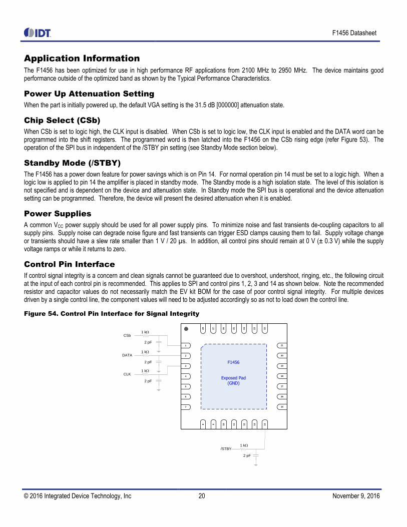
Control Pin Interface
If control signal integrity is a concern and clean signals cannot be guaranteed due to overshoot, undershoot, ringing, etc., the following circuit at the input of each control pin is recommended. This applies to SPI and control pins 1, 2, 3 and 14 as shown below. Note the recommended resistor and capacitor values do not necessarily match the EV kit BOM for the case of poor control signal integrity. For multiple devices driven by a single control line, the component values will need to be adjusted accordingly so as not to load down the control line.
Figure 54. Control Pin Interface for Signal Integrity
7
6
5
4
3
2
1
15
16
17
18
19
20
21
14
13
12
11
1098
F1456
Exposed Pad(GND)
22
23
24
25
26
27
28
1 k
2 pF
/STBY
1 k
2 pF
CLK
1 k
2 pF
CSb
1 k
2 pF
DATA

F1456 Datasheet
© 2016 Integrated Device Technology, Inc 21 November 9, 2016
Evaluation Kit Picture
Figure 55. Top View
Figure 56. Bottom View

F1456 Datasheet
© 2016 Integrated Device Technology, Inc 22 November 9, 2016
Evaluation Kit / Applications Circuit
Figure 57. Electrical Schematic
GND
R3 VCC
R16
C2
RFOUT
R12
GND1
R13
CLK
CSb
R14
DATA
C9
GND4
C8
R2
C10
GND3
C11
C5C6C7
J4
12
R8
R9
R10
C4
R5
R6
R7
R1
R15
R4
J1
C3
C15 C16
J5
1 2 3
C13
VCC1
C14
VCC2
J3
VCC
VCC
J2
GND2
C12
R11
RFIN
VCC
C1
VCC
J7
2468
1357
B4B3B2B1
B5
VCC
VCC3
J61 2 3
Not All Components are used. Please
check the Bill of Material (BOM) table.
F1456
U1
CSb1
DATA2
CLK3
RSET4
GND5
RFIN6
GND7
NC
8
NC
9
NC
11
NC
12
NC
13
14
/ST
BY GND
15
RFOUT16
GND17
NC18
GND21G
ND
23
NC
24
VC
C2
8
GN
D2
7
NC
26
NC
25
NC
22
NC20
NC
10
NC19
EP
29

F1456 Datasheet
© 2016 Integrated Device Technology, Inc 23 November 9, 2016
Table 10. Bill of Material (BOM)
Part Reference QTY Description Manufacturer Part # Manufacturer
C1, C2 2 22 pF ±5%, 50V, C0G Ceramic Capacitor (0402) GRM1555C1H220J MURATA
C3 1 100 nF ±10%, 16V, X7R Ceramic Capacitor (0402) GRM155R71C104K MURATA
C4 1 1000 pF ±5%, 50V, C0G Ceramic Capacitor (0402) GRM1555C1H102J MURATA
C5, C6, C7 3 2 pF ±0.1pF, 50V, C0G Ceramic Capacitor (0402) GRM1555C1H2R0B MURATA
C12 1 10 uF ±20%, 16V, X6S Ceramic Capacitor (0603) GRM188C81C106M MURATA
R1 1 2.2 kΩ ±1%, 1/10W, Resistor (0402) ERJ-2RKF2201X PANASONIC
R4 - R7 4 0 Ω Resistor (0402) ERJ-2GE0R00X PANASONIC
R8 - R10, R16 4 1 kΩ ±1%, 1/10W, Resistor (0402) ERJ-2RKF1001X PANASONIC
J4 1 CONN HEADER VERT SGL 2 X 1 POS GOLD 961102-6404-AR 3M
J6 1 CONN HEADER VERT SGL 3 X 1 POS GOLD 961103-6404-AR 3M
J7 1 CONN HEADER VERT DBL 4 X 2 POS GOLD 67997-108HLF FCI
J1, J2 2 Edge Launch SMA (0.375 inch pitch ground, tab) 142-0701-851 Emerson Johnson
J3 1 Edge Launch SMA (0.250 inch pitch ground, round) 142-0711-821 Emerson Johnson
U1 1 VGA AMP F1456NKGK IDT
C8 - C11, C13 - C16, R2, R3, R11 - R15, J5
DNP
1 Printed Circuit Board F145X EVKIT REV 02

F1456 Datasheet
© 2016 Integrated Device Technology, Inc 24 November 9, 2016
Evaluation Kit Operation
Standby
Connector J6 allows the F1456 to be put into the standby mode. Connecting J6 pin 2 (the center pin) to Vcc the amplifier will be placed in normal operating mode. To put the F1456 into standby mode for very low power consumption ground J6 pin 2 (the center pin). If J6 pin 2 (the center pin) is left open, then the F1456 will default to the standby mode.
Figure 58. Image of J6 connector for Standby mode control
Serial Programming Pins
Connector J7 pins 1, 2, 4, 6, 8 are ground. Pin 3 is DATA, pin 5 is Clock (CLK), pin 7 is Chip Select (CSB).
Figure 59. Image of J7 connector for SPI

F1456 Datasheet
© 2016 Integrated Device Technology, Inc 25 November 9, 2016
Package Drawings
Figure 60. Package Outline Drawing NKG28 PSC-4606
BOTTOM VIEW
SIDE VIEW
TOP VIEW

F1456 Datasheet
© 2016 Integrated Device Technology, Inc 26 November 9, 2016
Recommended Land Pattern
Figure 61. Recommended Land Pattern

F1456 Datasheet
© 2016 Integrated Device Technology, Inc 27 November 9, 2016
Ordering Information
Orderable Part Number Package MSL Rating Shipping Packaging Temperature
F1456NKGK 6 x 6 x 0.9 mm QFPN 1 Tray -40° to +105°C
F1456NKGK8 6 x 6 x 0.9 mm QFPN 1 Tape and Reel -40° to +105°C
F1456EVBK Evaluation Board
F1456EVSK Evaluation Solution
Marking Diagram
1. Line 2 and 3 are the part number. 2. Line 4 “ZW” is Assembly Stepping. 3. Line 4 “yyww = 1629 has two digits for the year and week that the part was assembled. 4. Line 4 “L” denotes Assembly Site. 5. Line 5 “Q54E042PY” is the Assembly Lot number

F1456 Datasheet
Corporate Headquarters
6024 Silver Creek Valley Road San Jose, CA 95138 www.IDT.com
Sales
1-800-345-7015 or 408-284-8200 Fax: 408-284-2775 www.IDT.com/go/sales
Tech Support
www.IDT.com/go/support
DISCLAIMER Integrated Device Technology, Inc. (IDT) reserves the right to modify the products an d/or specifications described herein at any time, without notice, at IDT's sole discretion. Performance specifications and operating parameters of the described products are determined in an independent state and are not guaranteed to perform the s ame way when installed in customer products. The information contained herein is provided without representation or warranty of any kind, whether express or implied, including, but not limited to, the suitability of IDT's products for any particular purpose, an implied warranty of merchantability, or non-infringement of the intellectual property rights of others. This document is presented only as a guide and does not convey any license under intellectual property rights of IDT or any third parties. IDT's products are not intended for use in applications involving extreme environmental conditions or in life support systems or similar dev ices where the failure or malfunction of an IDT product can be reasonably expected to significantly affect the health or safety of users. Anyone using an IDT product in such a manner does so at their own risk, absent an express, written agreement by IDT. Integrated Device Technology, IDT and the IDT logo are trademarks or registered trademarks of IDT and its subsidiaries in the United States and other countries. Other trademarks used herein are the property of IDT or their respective third party owners. For datasheet type definitions and a glossary of common terms, visit www.idt.com/go/glossary. All contents of this document are copyright of Integrated Device Technology, Inc. All rights reserved
© 2016 Integrated Device Technology, Inc 28 November 9, 2016
Revision History
Revision Revision Date Description of Change
O 2016-November 09 Initial Release